KAYA ELECTRONICS MD5XR User Manual

1
MD-5XR
(MD-5XRAH33)
Document NO. LAB1402-1
Application Note
Copyright 2013 by MOVON, all rights reserved.

2
Module Features
-Bluetooth system v3.0+EDR, 2.1+EDR, 2.0+EDR Compliant
-Class 2 Level Output Power Available
-UART Bypass Mode Support
-Scatternet Support
-Support of all Bluetooth packet types (voice and data)
-Support of low power modes: Park, Sniff and Hold
-UART, USB and PCM Interface Available
-Built-in Reference Clock: 26MHz
-High performance Stereo Codec
(Default : SBC, applicable : apt-X, AAC, MP3)
-16Mbits Flash Memory
Document NO. LAB1402-1
-Enhanced Audibility and Noise Cancellation
-RoHS Compliant
Applications
-High Quality Stereo Wireless Headsets
-Hands-Free Car Kits
-Wireless Speakers
-Analogue and USB Multimedia Dongles
-Bluetooth-Enabled Automotive wireless Gateways.
Features
-Size (12.0 X 20.0 X 2.3 mm)
-Class2 Support
-Surface Mountable
-1.8V Power Supply for core
-3.3V Power Supply for Memory, USB, UART, GPIO
-Not built-in Antenna (Antenna gain: 0dBi)
※ Caution
1. POP Noise issue 발생 시 당사에서 지원이 불가능하기 때문에 I2S Audio 출력을 권장합니다.
2. If bag is opened and a module is not reflowed within 168 hours, then you must bake modules as below
- Module with Reel Packing : 45℃/ 12hours
- Module out of Reel Packing : 125℃/ 2hours
Copyright 2013 by MOVON, all rights reserved.

3
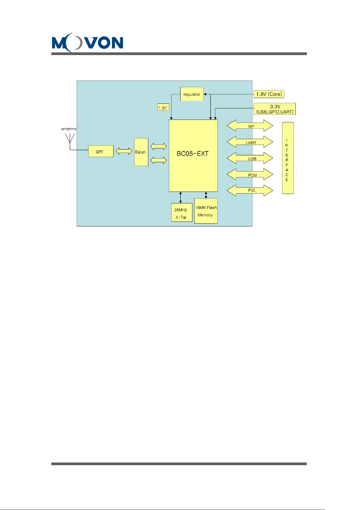
Overview
Document NO. LAB1402-1
Copyright 2013 by MOVON, all rights reserved.

4
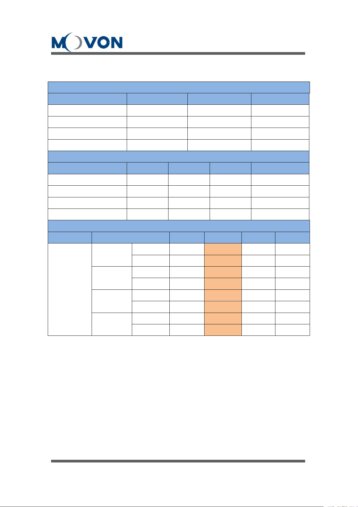
Absolute Maximum Ratings
Parameter
Min
Max
Unit
Storage Temperature
-40
+85
°C
VCC
-0.4
2.7
V
VDD_USB
-0.4
3.6
V
Other Pin Voltage
VSS-0.4
VDD_USB+0.4
V
Recommended Operating Conditions
Parameter
Min
Typ
Max
Unit
Operating Temperature
-40 / +85
°C
Humidity
/
+85 / %
VCC
1.7
1.8
1.95 V VDD_USB
3.0
3.3
3.6
V
Power Consumption (+25℃)
Parameter
Min
Typ
Max
Unit
Current
Discoverable
VCC
/
3.328
37.760
mA
VDD_USB
/
0.590
2.600
mA
Stand-by
VCC
/
3.071
8.995
mA
VDD_USB
/
0.591
2.720
mA
HFP
(with Alango)
VCC
/
43.992
51.400
mA
VDD_USB
/
8.314
8.830
mA
A2DP
VCC
/
33.299
41.400
mA
VDD_USB
/
0.591
8.650
mA
1. Electrical Characteristics
Document NO. LAB1402-1
Copyright 2013 by MOVON, all rights reserved.

5
Transmitter Performance
Parameter
Condition
Min
Typ
Max
Unit
Output Power
Normal/extreme test
-6 0 5
dBm
Power Density
Normal/extreme test
- - 20
dBm
Power Control
Normal/extreme test
Frequency Range
Normal/extreme test
2402
-
2480
MHz
20dB Bandwidth
Normal/extreme test
-
850
1000
KHz
Adjacent channel power
±2MHz
- - -20
dBm
±3MHz
- - -40
dBm
±4MHz
- - -40
dBm
Modulation Characteristics
ΔF1avg
140 - 175
KHz
ΔF2max
115 - -
KHz
ΔF2avg/ΔF1avg
- - 80
%
Initial Carrier Frequency Tolerance
-75 - 75
KHz
Carrier Frequency Drift
One slot Packet(DH1)
-25 - 25
KHz
Three slot Packet(DH3)
-40 - 40
KHz
Five slot Packet(DH5)
-40 - 40
KHz
Transceiver Performance
Parameter
Condition
Min
Typ
Max
Unit
Out-of Band spurious Emissions
30MHz-1GHz
- - -36
dBm
1GHz-12.75GHz
- - -30
dBm
1.8GHz-5.3GHz
- - -47
dBm
5.1GHz-5.3GHz
- - -47
dBm
Receiver Performance
Parameter
Condition
Min
Typ
Max
Unit
Sensitivity level
Single slot packets
-70
-83 - dBm
Sensitivity level
Multi slot packets
-70 - -
dBm
C/I performance
C/I co-channel
- 9 11
dB
C/I1MHz(adjacent channel)
-2 0 dB
C/I2MHz(2nd Adjacent channel)
-34
-30
dB
C/I≥3MHz(3
rd
adiacentchannel)
-43
-40
dB
Blocking performance
30MHz-2000MHz
-10 - -
dBm
2000MHz-2400MHz
-27 - -
dBm
2500MHz-3000MHz
-27 - -
dBm
2. RF specification
Document NO. LAB1402-1
Copyright 2013 by MOVON, all rights reserved.

6
3000MHz-12.75MHz
-10 - -
dBm
Intermodulation Performance
N=5
-39 - -
dBm
Maximum Input Level
-20
-5 - dBm
PIO No.
Pin Name
Description
Pad Type
1
PIO_11
Programmable input/output line
Bi-directional
2
PIO_12
Programmable input/output line
Bi-directional
3
PIO_13
Programmable input/output line
Bi-directional
4
PIO_14
Programmable input/output line
Bi-directional
5
USB_DP
USB Data Plus with selectable internal 1.5KΩ
Pull-up resistor
Bi-directional
6
USB_DN
USB Data minus
Bi-directional
7
VDD_USB
POWER FOR USB(3.3V)
Power
8
UART_RTS
UART request to send to active low
Bi-directional
9
UART_CTS
UART request to clear to active low
CMOS Input
10
UART_TX
UART Data Output
Bi-directional
11
UART_RX
UART Data Input
CMOS input
12
PIO_10
Programmable input/output line
Bi-directional
13
PIO_9
Programmable input/output line
CMOS Output
14
PIO_8
Programmable input/output line
CMOS Input
15
PIO_7
Programmable input/output line
Bi-directional
16
VSS
Common Ground
Ground
17
PIO_6
Programmable input/output line
Bi-directional
18
PIO_5
Programmable input/output line
Bi-directional
19
PIO_4
Programmable input/output line
Bi-directional
20
PIO_3
Programmable input/output line
Bi-directional
21
SPI_MOSI
SPI data input
CMOS input
22
SPI_CLK
SPI clock
Input
23
SPI_CSB
Chip select for SPI, active low
Input
24
SPI_MISO
SPI data output
CMOS output
25
LED_1
LED driver
Open drain
26
LED_0
LED driver
Open drain
27
PCM_CLK
Synchronous data clock
Bi-directional
28
PCM_SYNC
Synchronous data sync
Bi-directional
3. Pin Description
Document NO. LAB1402-1
Copyright 2013 by MOVON, all rights reserved.

7
29
PCM_IN
Synchronous data input
CMOS Input
30
PCM_OUT
Synchronous data output
CMOS output
31
VBAT
Battery Power
Power
32
PIO_2
Programmable input/output line
Bi-directional
33
PIO_1
Programmable input/output line
Bi-directional
34
PIO_0
Programmable input/output line
Bi-directional
35
VCHG
Charging Power
Power
36
VCC
Core Power(1.8V)
Power
37
MIC_BIAS
Microphone bias
Power
38
MIC_B_P
Microphone input positive, right
Analogue
39
MIC_B_N
Microphone input negative, right
Analogue
40
MIC_A_P
Microphone input positive, left
Analogue
41
MIC_A_N
Microphone input negative, left
Analogue
42
SPKR_B_N
Speaker output negative, right
Analogue
43
SPKR_B_P
Speaker output positive, right
Analogue
44
SPKR_A_N
Speaker output negative, left
Analogue
45
SPKR_A_P
Speaker output positive, left
Analogue
46
VSS
Common Ground
Ground
47
RF
RF connection to Antenna
Bi-directional
48
VSS
Common Ground
Ground
49
AIO_1
Analogue programmable in/out line
Bi-directional
50
AIO_0
Analogue programmable in/out line
Bi-directional
51
RST#
Reset if low. Input debounced so must be low
for>5ms to cause a reset
CMOS Input
52
VSS
Common Ground
Ground
Document NO. LAB1402-1
* If you want to use the MIC_BIAS of module, connect VBAT(31) to 3.3V.
(MIC_BIAS Voltage range: 1.7 ~ 3.3V)
But we don’t recommend using the Internal MIC_BIAS because of noise issue.
* VCHG(35) pin can’t be used.
Copyright 2013 by MOVON, all rights reserved.

8
Document NO. LAB1402-1
4. UART Interface
This is a standard UART interface for communicating with other serial devices.
MD-5XR UART interface provides a simple mechanism for communicating with other serial
devices using the RS232 protocol.
UART configuration parameters, such as baud rate and packet format, are set using MD-5XR
firmware.
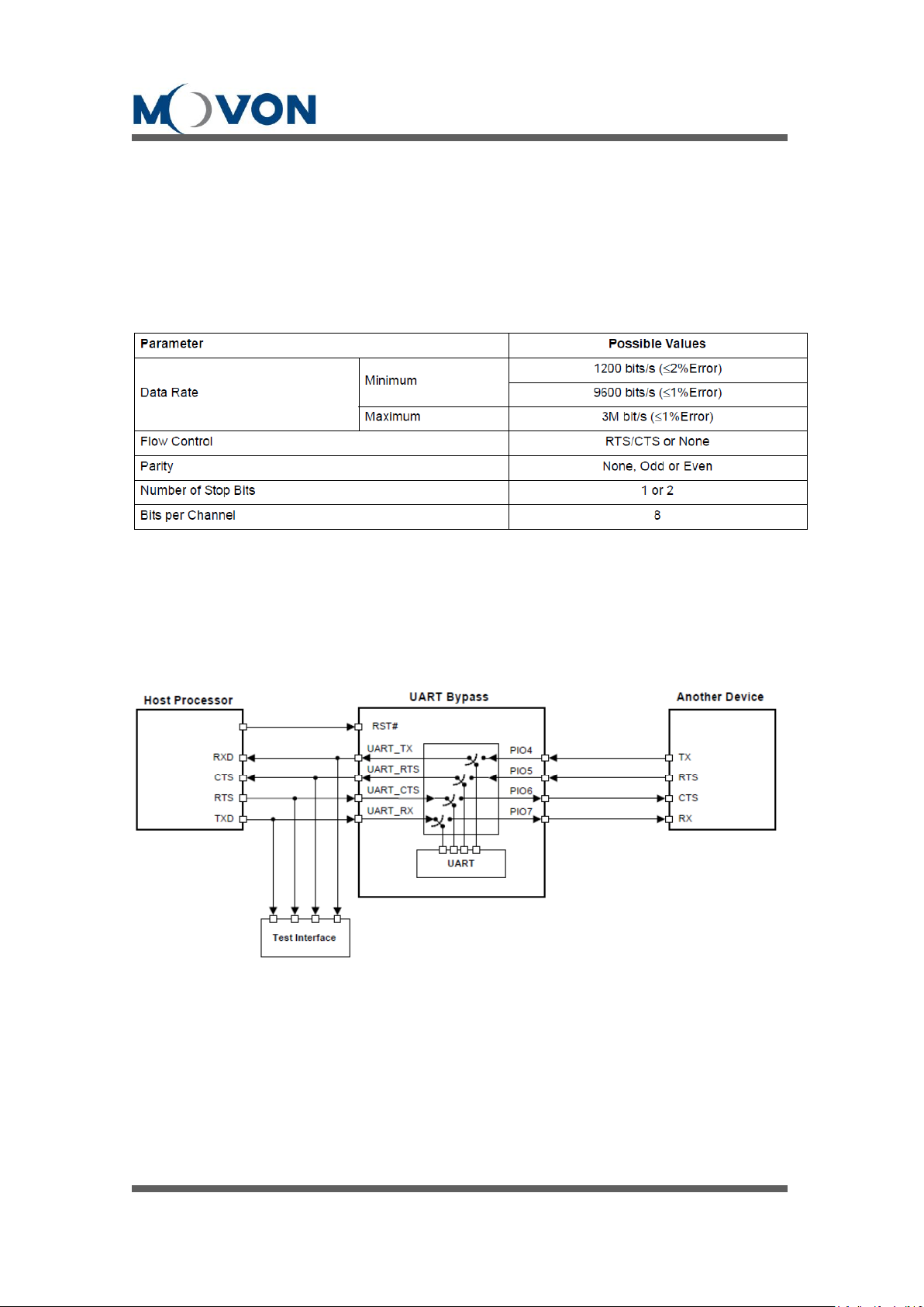
4.1 UART Bypass Mode
To apply the UART bypass mode, a BCCMD command is issued to MD-5XR. Upon this issue, it
switches the bypass to PIO[7:4] as shown in figure. When the bypass mode has been invoked,
MD-5XR enters the Deep Sleep state indefinitely.
Copyright 2013 by MOVON, all rights reserved.
 Loading...