

Kawasaki LSI KL5KUSB2CF Datasheet
KL5KUSB2CF
USB 2.0 Controller – Quick Interface
1
Ver. 1.5
PRELIMINARY
USB Interface
16 Bit Address / Data Bus
Data -
Data +
X2
X1
A15-0
D15-0
Cntrl.
2 IRQ
I2C
UART
I/o
Txd
Rxd
INT1-0
DIO2CK
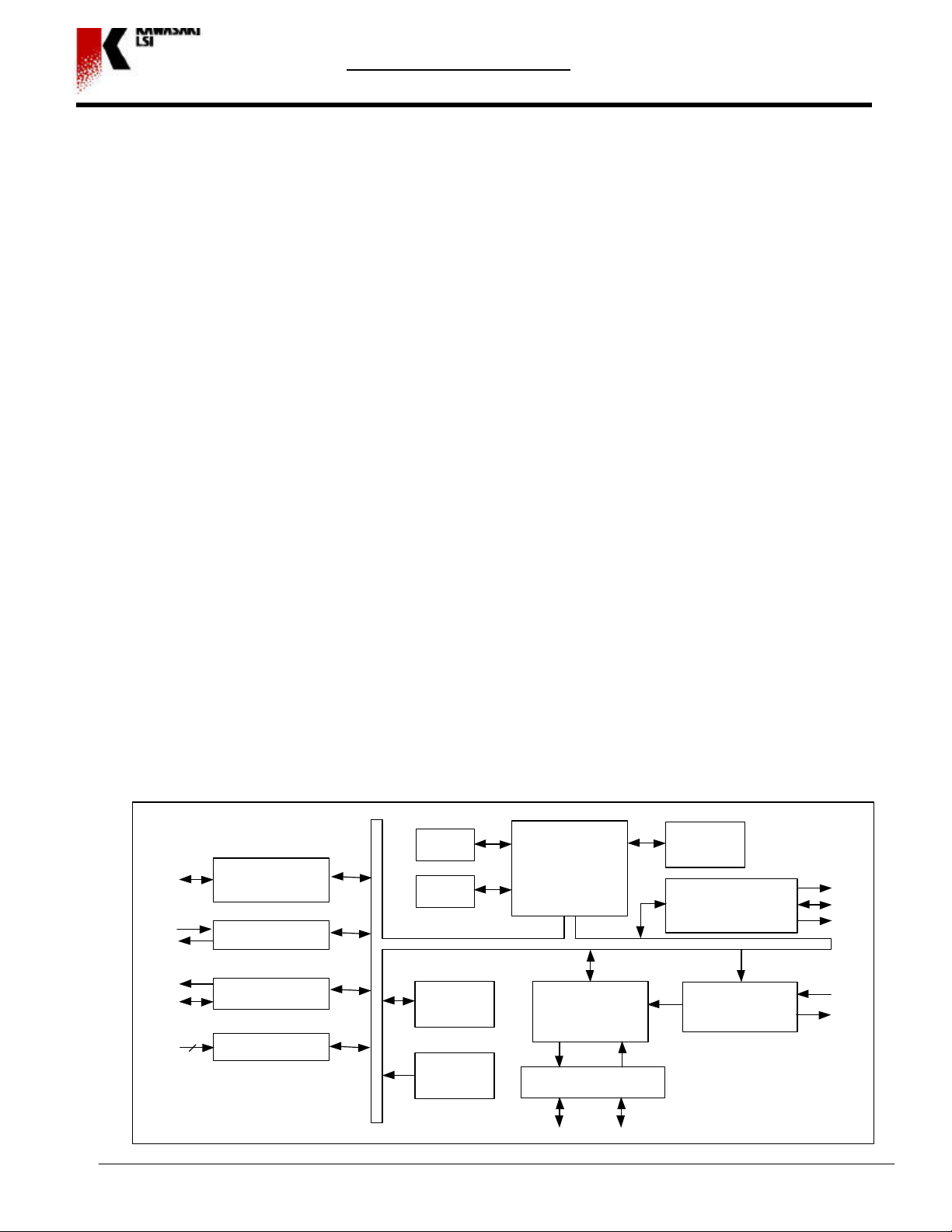
General Description
The Kawasaki KL5KUSB2CF Controller is a quick single chip solution to interface peripheral devices to
the Universal Serial Bus (USB) 2.0 specification. The KL5KUSB2CF has been specifically designed to
provide a simple and fast method of designing interfaces for peripheral devices to the USB port. This has
been accomplished by its highly integrated functionality and flexible General Purpose I/O (GPIO) that can
be configured to your system requirements. This device has been configured with a wide range of
capabilities for your immediate use or evaluation. The device can then be reconfigured for your specific
application. You can directly access the embedded processor’s address and data lines to use external
programmable logic for evaluation before configuring the GPIO for your final device. The SIE (Serial
Interface Engine) is fully compatible with the USB specification.
Features
• Advanced 16 Bit processor for USB transaction
processing and control data processing
• USB interface ver 2.0 compliant
• Transceivers and SIE (Serial Interface Engine)
• Internal Clock Generation
• Utilizes low cost external crystal circuitry
• 1.5K x 16 Internal RAM buffer
• 2 IRQ
• 8 Channel, 10 Bit A/D
Block Diagram (Application Example)
Timer 0
User Config.
Gates
Timer 1
• External Memory Interface for direct
access to the 16-bit processor for using
external logic or memory.
• User configurable gates
• Watchdog timer
• 8K user programmable gates
• 8K bytes ROM
• I2C Interface
• 100 pin QFP package
Watchdog
16 Bit
Processor
Timer
External Memory
Interface
Kawasaki LSI • 2570 North First Street • Suite 301 • San Jose, CA 95131 • Tel: (408) 570-0555 • Fax: (408) 570-0567 • www.klsi.com
RAM
(3KB)
Mask ROM
(8KB)
Serial
Interface
Engine
PLL & Clock
Generator
KL5KUSB2CF
USB 2.0 Controller – Quick Interface
2
Ver. 1.5
PRELIMINARY
Gates
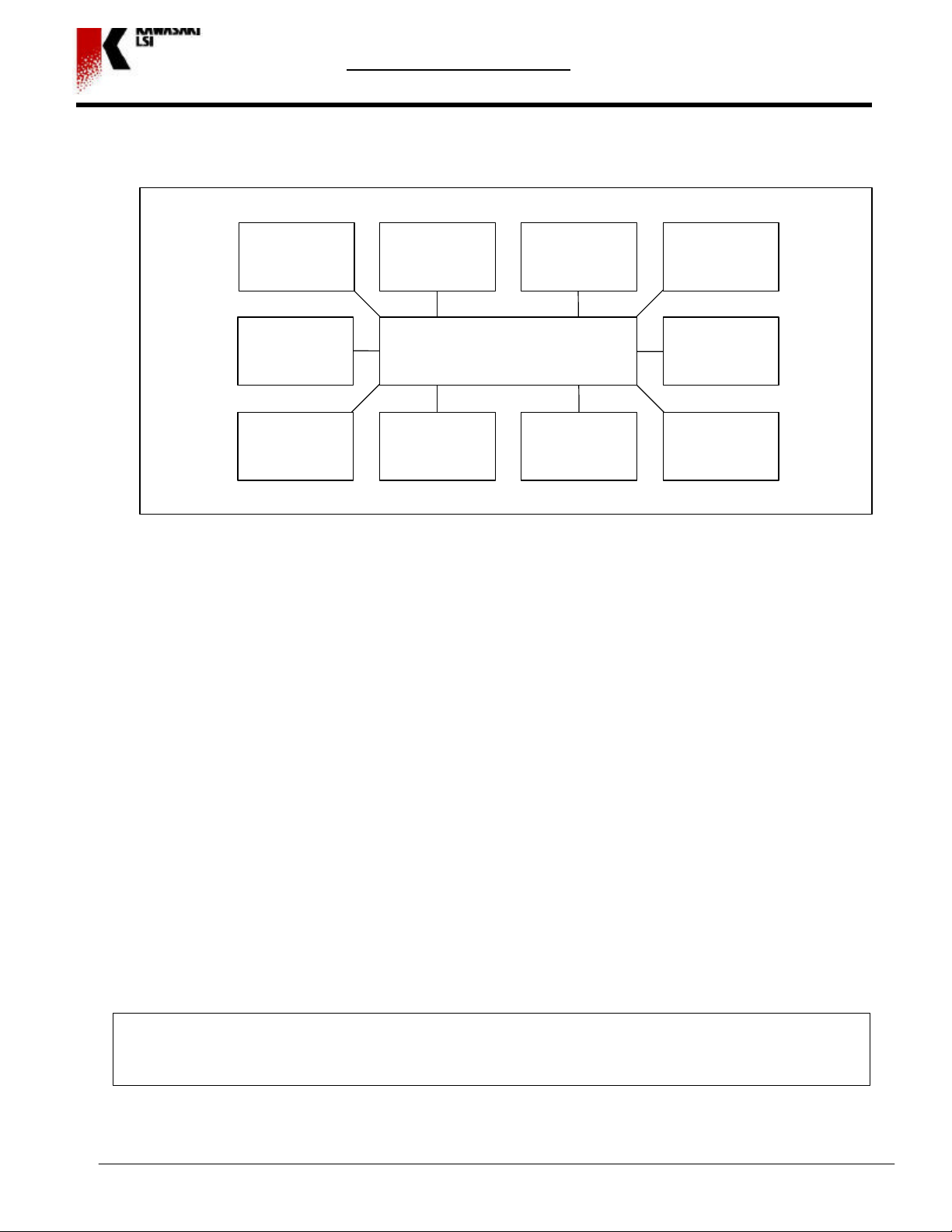
KL5KUSB2CF Basic Blocks
Programmable
Logic for
GPIO
USB Engine
and
Interface
Timer 0
Timer 1
Configured
GPIO
RAM
Custom Logic
16 Bit Micro
Interface
Watchdog
Timer
Mask ROM
for External
E2 Device
Avail.
PLL Clock
Generator
Kawasaki LSI assumes no responsibility or liability for (1) any errors or inaccuracies contained in the information herein and (2) the use of the
information or a portion thereof in any application, including any claim for (a) copyright or patent infringement or (b) direct, indirect, special or
consequential damages. There are no warranties extended or granted by this document. The information herein is subject to change without notice
form Kawasaki LSI
Kawasaki LSI • 2570 North First Street • Suite 301 • San Jose, CA 95131 • Tel: (408) 570-0555 • Fax: (408) 570-0567 • www.klsi.com
May 2000 • Copyright 2000 • Kawasaki LSI • Printed in U.S.A
 Loading...