Kawasaki LSI KL5KUSB221 Datasheet

KL5KUSB221
USB2.0 to 100Base-T Ethernet Controller
Kawasaki LSI • 2570 North First Street • Suite 301 • San Jose, CA 95131 • Tel: (408) 570-0555 • Fax: (408) 570-0567 • www.klsi.com
1
Ver. 1.0
PRELIMINARY
General Description
The Kawasaki KL5KUSB221 Controller is a unique single chip solution to interface peripheral
devices to the Universal Serial Bus 2.0 (USB2.0) and 100Base-T Ethernet. The KL5KUSB221
has been specifically designed to provide a simple solution to communicate with Ethernet
applications as well as other USB peripheral devices. This has been accomplished by its highly
integrated functionality. The USB controller consists of a central 16-bit processor, mask ROM,
RAM buffer, clock generator, Ethernet interface, UART, IRQ, Watchdog Timer, Serial interface,
External Memory Interface and SPORT Interface. The SIE (Serial Interface Engine) is fully
compatible with the USB2.0 specification. Our powerful internal processor enables Remote NDIS
(Network Drive) which gives compatibility with next generation operating systems and faster data
transfer. This USB to Ethernet controller is ideal for LAN (Local Area Network), HAN (Home Area
Network), Cable Modem, Set Top Boxes, or Mobile Networking applications.
Features
• Advanced 16 Bit processor for USB transaction
processing and control data processing
• 100Base-T compatibility
• USB interface version 2.0 compliant
• Transceivers and SIE (Serial Interface Engine)
• Internal Clock Generation - Utilizes low cost
external crystal circuitry
• MII Physical Layer interface
• 1.5K x 16 Internal RAM buffer
• Remote NDIS for faster data transfer.
• Fully IEEE compliant 100 Mbit/sec
Ethernet MAC Layer. Interfaces serially of
an external ENDEC PHY.
• UART
• External memory interface
• 100 LQFP package
• Serial Interface for external EEPROM
Block Diagram
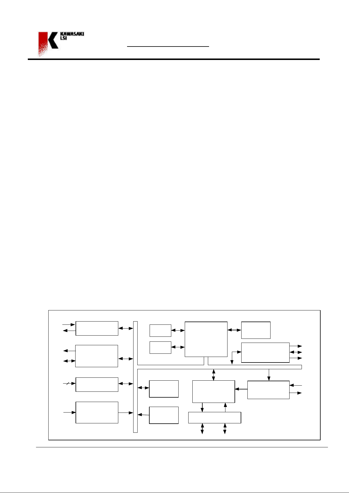
RAM
(3KB)
Timer 0
USB Interface
16 Bit Address / Data Bus
Data -
Data +
Serial
Interface
Engine
Mask ROM
(8KB)
Timer 1
Watchdog
Timer
16 Bit
Processor
UART
Txd
Rxd
10/100 Mb/s
Ethernet
Interface
MII PHY
Interface
EEPROM
Serial Interface
DIO
CK
SRAM Interface
A15-0
D15-0
Cntrl.X2X1
Clock Gen. &
Internal PLL
IRQ
INT 1-0
2

KL5KUSB221
USB2.0 to 100Base-T Ethernet Controller
Kawasaki LSI • 2570 North First Street • Suite 301 • San Jose, CA 95131 • Tel: (408) 570-0555 • Fax: (408) 570-0567 • www.klsi.com
2
Ver. 1.0
PRELIMINARY
February 23, 2000 • Copyright 2000 • Kawasaki LSI • Printed in U.S.A
Kawasaki LSI assumes no responsibility or liability for (1) any errors or inaccuracies contained in the information herein and (2) the use of the
information or a portion thereof in any application, including any claim for (a) copyright or patent infringement or (b) direct, indirect, special or
consequential damages. There are no warranties extended or granted by this document. The information herein is subject to change without notice
form Kawasaki LSI
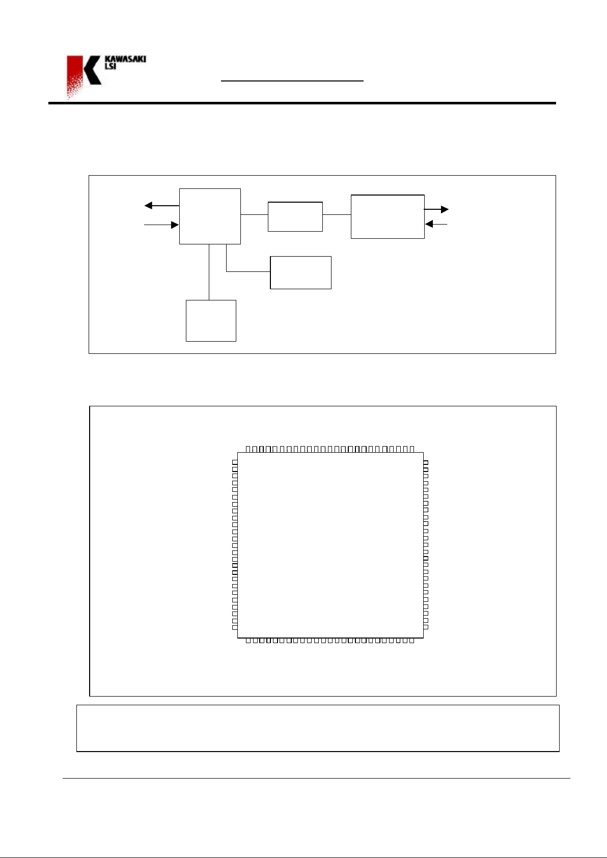
KL5KUSB221 Application Block Diagram
Pin Diagram 100LQFP
VDD
GND
VCO_IN
CP_OUT
PLLEN
VDD
N/C
PHRXD1
PHRXD2
PHRXD3
PHRXER
PHRXDV
GND
PHTXD0
PHCOL
PHTXEN
PHTXD1
PHTXD2
PHTXD3
PHTXER
GND
TXD
UGND
VP
VM
UVDD
N/C
N/C
PHTCLK
PHRXCLK
PHCRS
PH_RXD0
X_PCLK
RXD
IRQ0
IRQ1
DXA
TSCA
FS
VDD
SERROMD
SERROMCLK
PU#1
PCLK
DRA
GND
CLK
X2
XA_15
VDD
XA_7
XA_6
XA_5
XA_4
XA_3
XA_2
XA_1
nTST
nRESET
nXROMSEL
nXWR
nXRD
GND
nPDN
GND
VDD
N/C
N/C
LED_ON
nXRAMSEL
IGND
nXBHE
XA_0
XA_14
OVDD
VDD
XD_15
XD_14
OGND
XD_13
XD_12
IGND
XD_11
XD_10
XD_9
XD_8
XD_7
XD_6
XD_5
XD_4
XD_3
XD_2
XD_1
XD_0
XA_13
XA_12
XA_11
XA_10
XA_9
XA_8
1
2
3
4
5
6
7
8
9
10
11
12
13
14
15
16
17
18
19
20
21
22
23
24
25
75
74
73
72
71
70
69
68
67
66
65
64
63
62
61
60
59
58
57
56
55
54
53
52
51
100
9998979695949392919089888786858483828180797877
76
26272829303132333435363738394041424344454647484950
KL5KUSB221_L
Optional
External
Memory
Serial
EEPROM
KL5KUSB221
USB /
Ethernet
PHY
Transformer
USB
2.0
Full duplex
10/100 Base–T
Ethernet MII Interface
 Loading...