Kawasaki LSI KL5KUSB201 Datasheet

Kawasaki USB device KL5KUSB201
Datasheet (digest)
rev 1.1E page 1/21
KL5KUSB 201
USB2.0 Compliant Transceiver Chip
Datasheet (Digest)
Rev 1. 1E (2002.4.8)
Kawasaki Microelectronics Inc.
Kawasaki LSI Inc.
Copyright © 2002 Kawasaki Microelectronics Inc. Kawasaki LSI Inc . All rights reserved.

Kawasaki USB device KL5KUSB201
Datasheet (digest)
Intellectual Property Disclaimer and Copyright Notice
・ KAWASAKI MICROELECTRONICS INC. DISCLAIMS ALL LIABILITY, INCLUDING LIABILITY FOR INFRINGEMENT OF ANY
PROPRIETY RIG HTS, RE LATING TO USE OF INFORMATION IN T HIS DO CUMENT .
・ THIS DOCUMENT IS PROVIDED “AS IS” WITH NO WARRANTIES WHATSOEVER, INCLUDING ANY WARRANTY OF
MERCHANTABILITY, NON-INFRINGEMENT, FITNESS FOR ANY PARTICULAR PURPOSE, OR ANY WARRANTY
OTHERWISE ARISING OUT OF ANY PROPOSAL, SPECIFICATION OR SAMPLE.
・ KAWASAKI MICROELECTRONICS INC. RESERVES THE RIGHT TO MAKE ANY CHANGES, A T ANY TIME, WITHOUT
NOTICE, THE DESCRIPTION IN THIS DOCUMENT.
・ NEITHER THE WHOLE NOR ANY PART OF THE INFORMATION CONTAINED IN, OR THE PRODUCT DESCRIBED IN
THIS DOCUMENT MAY BE ADAPTED OR REPRODUCED IN ANY MATERIAL FORM EXCEPT WITH THE PRIOR
WRITTEN PERMISSION OF KAWASAKI MICRO
・ KAWASAKI PRODUCTS ARE NOT INTENDED FOR USE IN MEDICAL, LIFE SAVING, OR LIFE SUSTAINING
APPLICATI ONS.
rev 1.1E page 2/21
・ ALL PRODUCT NAMES A RE TRADEMARKS, REGISTERED TRADEMAR KS, OR SERVICE MARKS OF THEIR
RESPECTIVE OWNERS.
Copyright © 2002 Kawasaki Microelectronics Inc. Kawasaki LSI Inc . All rights reserved.

Kawasaki USB device KL5KUSB201
Datasheet (digest)
Revision History
revision date Update
0.10J 2001.9.28 release first version
0.21J 2001.10.18 minor error cor rection
0.30E 2002.3.15 translation from Japanese to English with some minor change
1.0E 2002.3.25 Document Review is closed.
1.1E 2002.4.8 Table 5-3 pin78, 79 error corrected.
rev 1.1E page 3/21
Copyright © 2002 Kawasaki Microelectronics Inc. Kawasaki LSI Inc . All rights reserved.

Kawasaki USB device KL5KUSB201
Datasheet (digest)
Table of Cont en ts
1. Overview 5
1.1 Chip Functionality 5
1.2 KL5KUSB201 Product Feature 6
2. Chip Architecture 6
3. Application Example 8
4. Pinout Diagram 8
5. Package Information 9
5.1 Top View 9
5.2 Package Size 10
5.3 Pin Assignment 10
6. Signal Description 11
7. SIE Bus Timing 13
rev 1.1E page 4/21
7.1 SIE Bus Output Timing 13
7.2 SI E B u s I npu t Timi n g 13
8. USB Bus Timing 14
8.1 Bulk IN Transaction 14
8.2 Bulk OUT Transaction 15
9. USB2.0 LSI Family 15
9.1 T&MT Evaluation Daughter Card (UUT) 15
9.2 PC I E v aluation Add-in C a r d 16
9.3 KL5BUDV002 LSI (U2PCI) 17
9.4. USB201 and HS_SIE ASIC IP 19
9.4.1 HS_SIE ASIC IP 19
9.4.2 USB201 ASIC IP 20
10. References 21
Copyright © 2002 Kawasaki Microelectronics Inc. Kawasaki LSI Inc . All rights reserved.

Kawasaki USB device KL5KUSB201
Datasheet (digest)
1. Overview
Kawasaki Microelectronics Inc. and Kawasaki LSI Inc. introduce KL5KUSB201 LSI,
which is designed based on USB Specification revision 2.0 and operates as both
USB2.0 High Speed and Full Speed transceiver chip. It has two modes – UTMI
Specification compatible mode and Kawasaki Original mode. In Kawasaki Original
mode, th e LSI ha s sev eral con veni ent fun cti on s uch a s au tom ati c CRC gener ati on and
verification, transmit packet abortion and automatic test packet generation for High
Speed Signal Quality test. The LSI is recognized as USB2.0 PHY chip and customers
are able to build up USB2.0 compliant device system with their logic and PHY control /
endpoint buffer function (SIE), which is available by Kawasaki or other IP vendor.
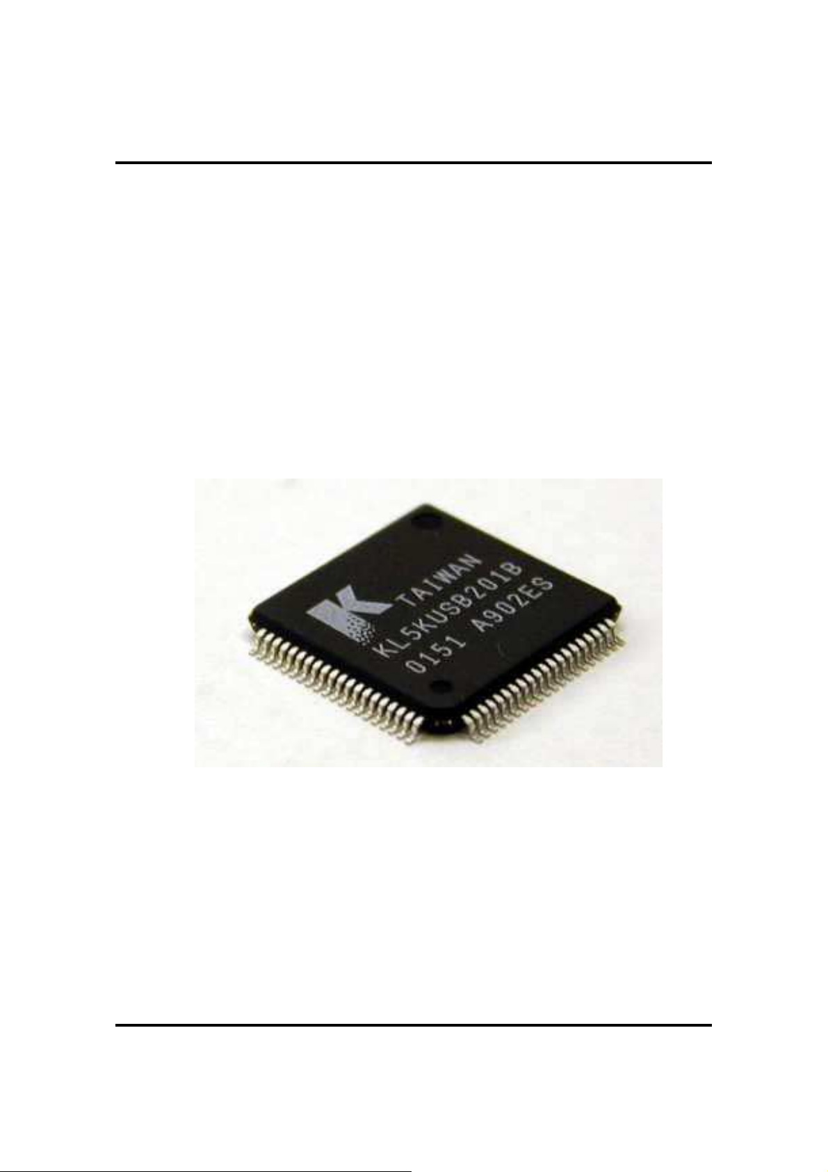
Figure 1. KL5KUSB201 Image
rev 1.1E page 5/21
1.1 Chip Functionality
KL5KUSB201 Fucntionality is summarized below.
1. HS Chirp Signal Generation and Detection
2. Support for both High Speed (480Mbit/sec) and Full Speed (12Mbit/sec)
3. For received packet, phase lock, buffering, SYNC detection, NRZI decode, bit
un-stuffing, CRC error detection (optional), serial to parallel conversion are
performed. 16bit data is drived on SIE bus
4.For packet transmission, parallel 16bit data is received, serialized, CRC
Copyright © 2002 Kawasaki Microelectronics Inc. Kawasaki LSI Inc . All rights reserved.

Kawasaki USB device KL5KUSB201
Datasheet (digest)
generation (optional), bit stuffed and NRZI encoded. Packet is transmitted onto
USB bus with SYNC and EOP attached
5. USB Bus status is delivered for outside SIE to monitor it
6. Function is controlled by Input Signals
7. Function defined by UTMI Specification is supported
8. Stand-alone Test packet generation for High Speed Signal Quality
1.2 KL5KUSB201 Product Feature
KL5KUSB201 Product Feature is shown below.
Table 1-2 KL5KUSB201 Product Feature
No Item Feature
1 Process 0.18um CMOS
2 Packag e LQFP 80 pin plastic package
3 Input Clock Frequency 48MHz
4 Internal Clock Frequency
5 Output Clock Frequency
(CKOUT)
6 USB port 1 port
7 Parallel Data width (SIE_DAT) 16bit
8 Power voltage
9 Operation Current in FS typical 50mA
10 Operation Current in HS typical 90mA
11 Operation Current at suspend 1uA
12 Ambient Temperature
480MHz、48MHz and other
30MHz
(USB pin is separated for HS and FS)
3.3±0.3V、1.8±0.15V
0~70°C
rev 1.1E page 6/21
Please contact to our sales and marketing person to request samples, datasheet,
USB201 IP and / or HS_SIE included ASCP planning.
2. Chip Architecture
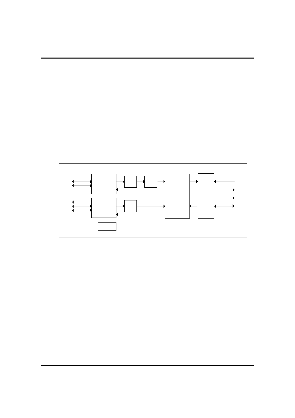
Internal Architecture of KL5KUSB201 is shown in figure 2. The LSI consists of 6 major
blocks as follows. FrontEnd block transmits and receives USB signals. HS DLL
block is used to re-clock High Speed signals with internal 480MHz clock. EBUF block
is for buffering High Speed signals. Shared Logic block includes such function as
NRZI decode, bit un-stuffing, CRC check, serial to parallel conversion for both High
Speed and Full Speed USB sig nals. SIE _IF blo ck in terf ac es wi th SI E bu s si gnal s. Fo r
Full Speed operation, DPLL block is used to re-clock the Full Speed signals with
Copyright © 2002 Kawasaki Microelectronics Inc. Kawasaki LSI Inc . All rights reserved.

Kawasaki USB device KL5KUSB201
Datasheet (digest)
internal 12 MHz clock instead of FrontEnd, HSDLL and EBUF blocks. For receiv ed
signals, the LSI locks them in HS DLL and is bufferi ng them in EBUF. Then signals
are transf erred to Shared Logi c to co nvert data format, check th e CRC, convert from
serial to parallel. The data is finally delivered to the SIE bus through SIE_IF. For
transmit operation, incoming parallel data is received in SIE_IF and sent to Shared
Logic to perform parallel t o serial conversion , CRC generation, bi t stuffing and NRZI
encoding. Finally the data is transmitted onto the USB bus through FrontEnd block.
High Speed or Full Speed operation is selected by SIE control signals. USB bus status
can be monitored by USB bus status signals.
Figure 2 KL5KUSB201 Internal Architecture
USB bus SIE bus
HSDP
HSDM
RPU_ENA
FSDP
FSDM
HS
FrontEnd
FS
FrontEnd
HS
DLL
DPLL
EBUF
Shared
Logic
rev 1.1E page 7/21
CTRL
STATUS
SIE_IF
CKOUT
SIE_DAT
External
48MHz clock
CLK
GEN
Copyright © 2002 Kawasaki Microelectronics Inc. Kawasaki LSI Inc . All rights reserved.
 Loading...