

Kawasaki LSI KL5KUSB200 Datasheet
KL5KUSB200
1
Ver. 2.2
Status
Control Signals
SIE_Data
Full Speed
DPLL
HS
DLL
EBUF
HSDM
HSDP
RPU_ENA
FSDP
FSDM
CKOUT
SIE Bus
USB Bus
Clock
External
USB2.0 Transceiver
General Description
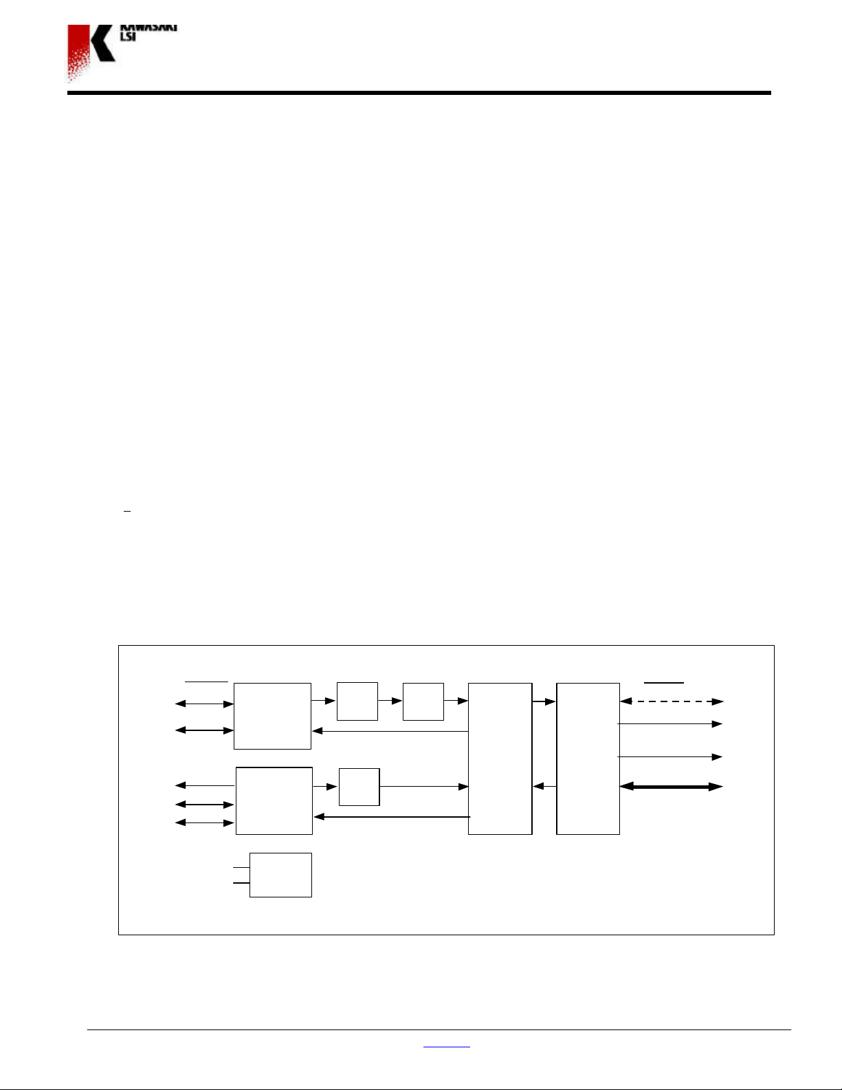
The Kawasaki USB 2.0 Compliant Transceiver is the interface between the high performance USB serial
bus and the 16-bit SIE bus. The high-speed analog interface and the digital serial bit processing feature
of the USB 2.0 transceiver enables a highly integrated USB 2.0 device. The transceiver is controlled by
input signals from the SIE bus which is synchronized with the 30MHz clock output. The Kawasaki
Transceiver also provides output signals to monitor the USB bus status. The Kawasaki Transceiver, SIE,
and logic design are combined to create Kawasaki's USB chip solutions for peripheral devices or can be
used as IP with our ASIC technology.
Features
• USB 2.0 compliant transceiver
• UTMI based design (USB 2.0 Transceiver Macro
cell Interface)
• Generates 48MHz to 480MHz input
• Full Speed / High Speed capabilities
• Supports “Chirp” for High Speed recognition
• Support Reset and Suspend
• Operational mode selection
Block Diagram
High Speed
Front end
• Status signals for monitoring USB bus
• Optional CRC verification/generation logic
• Mode bit expansion for device test
• 16 bit Bi-directional SIE bus
• TX data packet abort
• ASIC IP supports High speed SIE with
ASIC IP
• 80 pin LQFP package (12 mm2)
Shared
Logic
SIE
Interface
Front end
48MHz Clk
US: Kawasaki LSI , 2570 N. 1st Street, San Jose, CA 95131,Tel:(408) 570-0555, Fax(408) 570-0567, www.klsi.com
Japan: Kawasaki Steel Corp, Makuhari Techno-Garden B5, Nakase 1-3, Mihama-ku, Chiba, 261-8501Tel:(043)296-3283, Fax:(043)296-3285, email:usb-info@lsidv.kawasaki-steel.co.jp
Generator
KL5KUSB200
2
Ver. 2.2
Kawasaki LSI assumes no responsibility or liability for (1) any errors or inaccuracies contained in the information herein and (2) the use of the information or a portion thereof in any application,
A1VDD
RSTN
SUSPN
DAT[0]
0VDD
0GND
DAT[1]
DAT[2]
IGND
DAT[3]
ICVDD
CGND
DAT[4]
0GND
0VDD
DAT[5]
DAT[6]
ICVDD
CGND
SIE_DAT[15]
1
HS D+
HS D-
D-
D+
Rs
Rs
Rpu
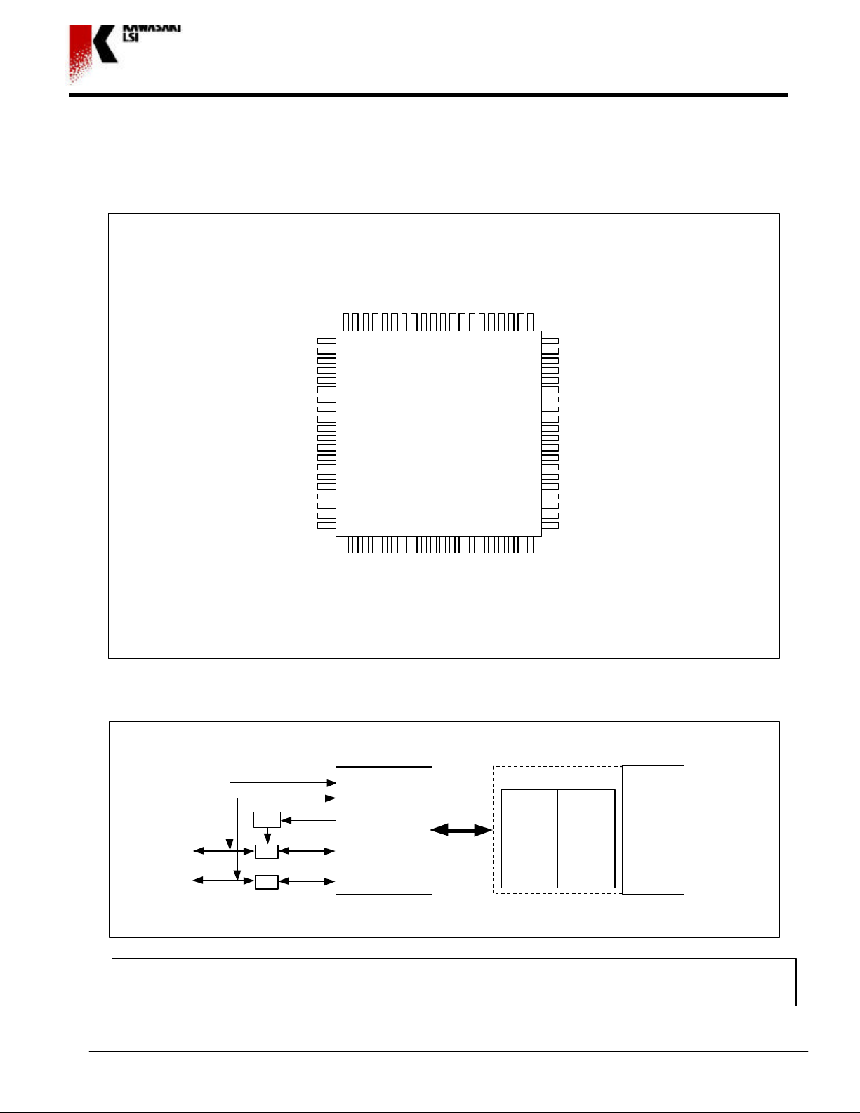
Pin Diagram 80LQFP
2
A1GND
A2VDD
3
4
A2GND
REXT
5
UVDD
UGND
FSDP
HSDP
HSDM
FSDM
UGND
UVDD
ICVDD
MODE[0]
MODE[1]
IGND
MODE[2]
MODE[3]
6
7
8
9
10
11
12
13
14
15
16
17
18
19
20
RPU_ENA
0GND
XOUT
XIN
0VDD
RXACT
RXVLD
0GND
CRCERR
RXERR
TXRDY
WDVLD
ICVDD
CGND
TXACT
CRCACT
IGND
FS_HSN
80797877767574737271706968676665646362
PU_SEON
KL5KUSB200
USB 2.0
Transceiver
ICVDD
CGND
61
USB2.0 Transceiver
60
CKOUT
59
0VDD
58
0GND
57
ICVDD
56
CGND
55
SIE_DAT[14]
54
SIE_DAT[13]
53
IGND
52
SIE_DAT[12]
51
CGND
50
SIE_DAT[11]
49
SIE_DAT[10]
48
0VDD
47
0GND
46
ICVDD
45
CGND
44
SIE_DATA[9]
43
SIE_DATA[8]
42
SIE_DATA[7]
41
21222324252627282930313233343536373839
Application Block Diagram
RPU_ENA
KL5KUSB200
BSTAT[0]
BSTAT[1]
SIE_
SIE_
SIE_
SIE_
SIE_
SIE_
SIE_
Control
Logic
40
User
Endpoint
Logic
Buffer
including any claim for (a) copyright or patent infringement or (b) direct, indirect, special or consequential damages. There are no warranties extended or granted by this document. The
information herein is subject to change without notice form Kawasaki LSI
Oct 2000 • Copyright 2000 • Kawasaki LSI • Printed in U.S.A
US: Kawasaki LSI , 2570 N. 1st Street, San Jose, CA 95131,Tel:(408) 570-0555, Fax(408) 570-0567, www.klsi.com
Japan: Kawasaki Steel Corp, Makuhari Techno-Garden B5, Nakase 1-3, Mihama-ku, Chiba, 261-8501Tel:(043)296-3283, Fax:(043)296-3285, email:usb-info@lsidv.kawasaki-steel.co.jp
 Loading...