

Kawasaki LSI KL5KUSB121 Datasheet
KL5KUSB121
USB to 10/100 Ethernet Controller
1
Ver. 1.1
PRELIMINARY
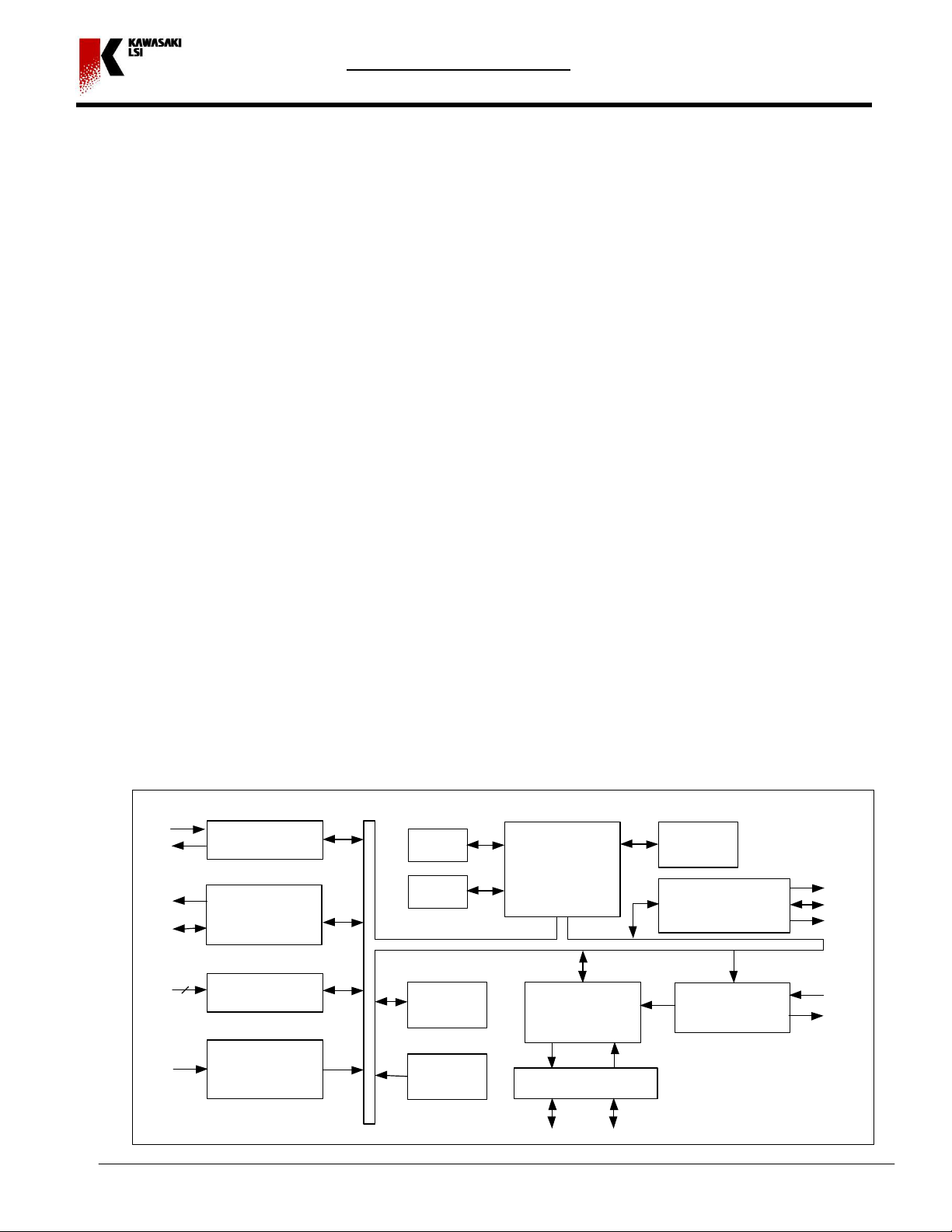
General Description
Timer 0
USB Interface
16 Bit Address / Data Bus
Data -
Data +
Timer 1
UART
Txd
Rxd
Interface
MII PHY
DIO
CK
SRAM Interface
A15-0
D15-0
Cntrl.X2X1
IRQ
INT 1-0
2
The Kawasaki KL5KUSB121 Controller is a unique single chip solution to interface peripheral
devices to the Universal Serial Bus (USB) and Ethernet. The KL5KUSB121 has been specifically
designed to provide a simple solution to communicate with Ethernet applications as well as other
USB peripheral devices. This has been accomplished by its highly integrated functionality. The
USB controller consists of a central 16-bit processor, mask ROM, RAM buffer, clock generator,
Ethernet interface, UART, IRQ, Watchdog Timer, Serial interface, External Memory Interface and
SPORT Interface. The SIE (Serial Interface Engine) is fully compatible with the USB specification.
Our powerful internal processor enables Remote NDIS (Network Drive) which gives compatibility
with next generation operating systems and faster data transfer. This USB to Ethernet controller
is ideal for LAN (Local Area Network), HAN (Home Area Network), Cable Modem, Set Top
Boxes, or Mobile Networking applications.
Features
• Advanced 16 Bit processor for USB transaction
processing and control data processing
• 10/100Base-T compatibility
• USB interface ver. 1.0/1.1 compliant
• Transceivers and SIE (Serial Interface Engine)
• Internal Clock Generation - Utilizes low cost
external 12MHz crystal circuitry
• MII Physical Layer interface
• 1.5K x 16 Internal RAM buffer
Block Diagram
EEPROM
Serial Interface
• Remote NDIS for faster data transfer.
• Fully IEEE 802.3 compliant 10 Mbit/sec
Ethernet MAC Layer. Interfaces serially of
an external ENDEC PHY.
• UART
• External memory interface
• LQFP package
• Serial Interface for external EEPROM
Watchdog
16 Bit
Processor
Timer
Interface
Kawasaki LSI • 2570 North First Street • Suite 301 • San Jose, CA 95131 • Tel: (408) 570-0555 • Fax: (408) 570-0567 • www.klsi.com
10/100 Mb/s
Ethernet
RAM
(3KB)
Mask ROM
(8KB)
Serial
Interface
Engine
Clock Gen. &
Internal PLL
KL5KUSB121
USB to 10/100 Ethernet Controller
2
Ver. 1.1
PRELIMINARY
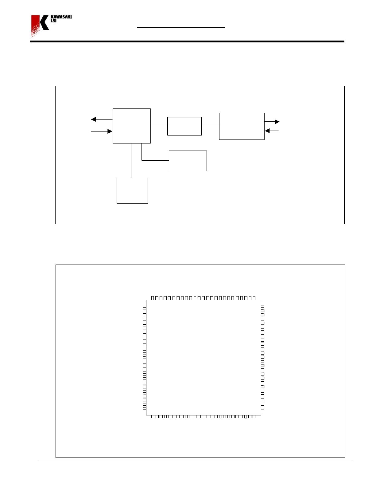
KL5KUSB121 Application Block Diagram
UVDD
N/C
N/C
PHRXCLK
RXD
IRQ0
IRQ1
DXA
FS
VDD
SERROMD
PU#1
PCLK
GND
CLK
X2
XA_15
VDD
XA_7
1
EEPROM
USB
KL5KUSB121
USB /
Ethernet
Optional
External
Memory
Pin Diagram 100LQFP
PHY
Transformer
Serial
VDD
XD_15
XD_14
OGND
XD_13
XD_12
IGND
XD_11
XD_10
XD_9
XD_8
XD_7
XD_6
XD_5
XD_4
XD_3
XD_2
XD_1
XD_0
XA_13
9998979695949392919089888786858483828180797877
100
XA_12
XA_11
XA_10
XA_9
Full duplex
10/100 Base – T
Ethernet MII
Interface
XA_8
76
Kawasaki LSI • 2570 North First Street • Suite 301 • San Jose, CA 95131 • Tel: (408) 570-0555 • Fax: (408) 570-0567 • www.klsi.com
VDD
GND
VCO_IN
CP_OUT
PLLEN
VDD
N/C
PHRXD1
PHRXD2
PHRXD3
PHRXER
PHRXDV
GND
PHTXD0
PHCOL
PHTXEN
PHTXD1
PHTXD2
PHTXD3
PHTXER
GND
TXD
UGND
VP
VM
2
3
4
5
6
7
8
9
10
11
12
13
14
15
16
17
18
19
20
21
22
23
24
25
26272829303132333435363738394041424344454647484950
KL5KUSB121_L
PHCRS
PHTCLK
X_PCLK
PH_RXD0
TSCA
DRA
SERROMCLK
75
XA_6
74
XA_5
73
XA_4
72
XA_3
71
XA_2
70
XA_1
69
nTST
68
nRESET
67
nXROMSEL
66
nXWR
65
nXRD
64
GND
63
nPDN
62
GND
61
VDD
60
N/C
59
N/C
58
LED_ON
57
nXRAMSEL
56
IGND
55
nXBHE
54
XA_0
53
XA_14
52
OVDD
51
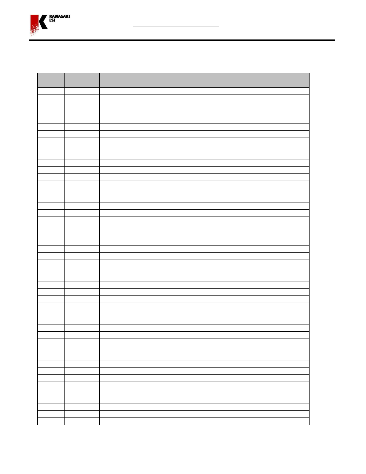
KL5KUSB121
USB to 10/100 Ethernet Controller
3
Ver. 1.1
PRELIMINARY
Pin Description
Pin #
LQFP
1 IN VDD VDD
2 GND GND PLL GND
3 IN VCO_IN PLL VCO IN
4 OUT CP_OUT PLL VCO OUT
5 IN PLLEN PLL Enable
6 IN VDD PLL VDD
7 N/C N/C Open connection
8 IN PHRXD1 PHY Receive Data 1
9 IN PHRXD2 PHY Receive Data 2
10 IN PHRXD3 PHY Receive Data 3
11 IN PHRXER Receive Data Error from PHY
12 IN PHRXDV Receive Data Valid from PHY
13 IN GND Ground
14 OUT PHTXD0 Transmit data to PHY
15 IN PHCOL Collision input from PHY
16 OUT PHTXEN Transmit Enable to PHY
17 OUT PHTXD1 Transmit Data 1 to PHY
18 OUT PHTXD2 Transmit Data 2 to PHY
19 OUT PHTXD3 Transmit Data 3 to PHY
20 OUT PHTXER Transmit Error to PHY
21 IN GND Ground
22 IN/OUT TXD UART TXD
23 IN UGND USB GND
24 IN/OUT VP USB + Pin
25 IN/OUT VM USB – Pin
26 IN UVDD USB VDD
27 NC NC Open connection
28 NC NC Open connection
29 IN PHTXCLK PHY Transmit Clock
30 IN PHRXCLK PHY Receive Clock
31 IN PHCRS PHY Carrier Sense
32 IN PH_RXD0 PHY Serial Receive Data
33 IN/OUT X_PCLK External PCLK
34 IN/OUT RXD UART RXD
35 IN IRQ0 Edge sens. Interrupt
36 IN IRQ1 Edge sens. Interrupt
37 OUT DXA Sport Mode or GPIO7
38 IN TSCA Sport Mode or GPIO8
39 IN/OUT FS Sport Mode or GPIO9
40 IN VDD Open connection
41 IN/OUT SERROMD Serial ROM Data
42 OUT SERROMCLK Serial ROM Clock
43 IN/OUT PU#1 Pull up to USB + Pin for High Speed
44 IN PCLK Sport Mode or GPIO5
45 IN DRA Sport Mode or GPIO6
46 IN OGND GND
47 IN CLK 12MHz Clock/Crystal Input
I/O Pin Name Description
Kawasaki LSI • 2570 North First Street • Suite 301 • San Jose, CA 95131 • Tel: (408) 570-0555 • Fax: (408) 570-0567 • www.klsi.com
KL5KUSB121
USB to 10/100 Ethernet Controller
4
Ver. 1.1
PRELIMINARY
Pin #
LQFP
48 OUT X2 12MHz Crystal Output
49 OUT XA_15 External Address Pin
50 IN VDD VDD
51 IN OVDD VDD
52 OUT XA_14 External Address Pin
53 OUT XA_0 External Address Pin
54 OUT nXBHE SRAM Byte High Enable
55 IN IGND GND
56 OUT nXRAMSEL SRAM Byte Low Enable
57 OUT LED_ON Turns on 3.3V to TX LED
58 N/C N/C Open connection
59 N/C N/C Open connection
60 IN VDD VDD
61 IN GND Ground
62 IN/OUT nPDN Active low Powerdown mode signal to Phy
63 IN GND GND
64 OUT nXRD External Memory Read (Active low)
65 OUT nXWR External Memory Write (Active low)
66 N/C nXROMSEL External ROM CS, active LO
67 IN nRESET Reset Pin
68 IN nTST Test Pin, Disconnect for Normal Operation
69 OUT XA_1 External Address Pins
70 OUT XA_2 External Address Pins
71 OUT XA_3 External Address Pins
72 OUT XA_4 External Address Pins
73 OUT XA_5 External Address Pins
74 OUT XA_6 External Address Pins
75 OUT XA_7 External Address Pins
76 OUT XA_8 External Address Pins
77 OUT XA_9 External Address Pins
78 OUT XA_10 External Address Pins
79 OUT XA_11 External Address Pins
80 OUT XA_12 External Address Pins
81 OUT XA_13 External Address Pins
82 IN/OUT XD_0 External Data Pins
83 IN/OUT XD_1 External Data Pins
84 IN/OUT XD_2 External Data Pins
85 IN/OUT XD_3 External Data Pins
86 IN/OUT XD_4 External Data Pins
87 IN/OUT XD_5 External Data Pins
88 IN/OUT XD_6 External Data Pins
89 IN/OUT XD_7 External Data Pins
90 IN/OUT XD_8 External Data Pins
91 IN/OUT XD_9 External Data Pins
92 IN/OUT XD_10 External Data Pins
93 IN/OUT XD_11 External Data Pins
94 IN IGND GND
95 IN/OUT XD_12 External Data Pins
96 IN/OUT XD_13 External Data Pins
97 IN OGND GND
I/O Pin Name Description
Kawasaki LSI • 2570 North First Street • Suite 301 • San Jose, CA 95131 • Tel: (408) 570-0555 • Fax: (408) 570-0567 • www.klsi.com

KL5KUSB121
USB to 10/100 Ethernet Controller
5
Ver. 1.1
PRELIMINARY
Pin #
LQFP
98 IN/OUT XD_14 External Data Pins
99 IN/OUT XD_15 External Data Pins
100 IN VDD VDD
I/O Pin Name Description
Function Description
16 Bit Processor
The integrated 16 bit processor serves as a micro controller for USB peripherals. The
processor can execute approximately five million instructions per second. With this
processing power it allows the design of intelligent peripherals that can process data prior
to passing it on to the host PC, thus improving overall performance of the system. The
masked ROM (4K X 16) in the KL5KUSB121 or external memory contains a specialized
instruction set that has been designed for highly efficient coding of processing algorithms
and USB transaction processing.
The 16-bit processor is designed for efficient data execution by having direct access to
the RAM Buffer, external memory, I/O interfaces, and all the control and status registers.
The divide/multiply feature expands the capability of USB peripherals.
The processor supports prioritized vectored hardware interrupts. In addition, as many as
240 software interrupt vectors are available.
The processor provides six addressing modes, supporting memory-to-memory, memoryto-register, register-to-register, immediate-to-register or immediate-to-memory
operations. Register, direct, immediate, indirect, and indirect indexed addressing modes
are supported. In addition, there is an auto-increment mode in which a register, used as
an address pointer is automatically incremented after each use, making repetitive
operations more efficient both from a programming and a performance standpoint.
The processor features a full set of program control, logical, and integer arithmetic
instructions. All instructions are sixteen bits wide, although some instructions require
operands, which may occupy another one or two words. Several special “ short
immediate” instructions are available, so that certain frequently used operations with
small constant operand will fit into a 16-bit instruction.
RAM Buffer
The USB controller contains a 3K byte (1.5K X 16) internal buffer memory. The memory
is used to buffer data and USB packets and accessed by the 16 Bit processor and the
SIE. USB transactions are automatically routed to the memory buffer. The 16-bit
processor has the ability to set up pointers and block sizes in buffer memory for USB
transactions. Data is read from the interface and is processed and packetized by the 16bit I/O processor.
Kawasaki LSI • 2570 North First Street • Suite 301 • San Jose, CA 95131 • Tel: (408) 570-0555 • Fax: (408) 570-0567 • www.klsi.com

KL5KUSB121
USB to 10/100 Ethernet Controller
6
Ver. 1.1
PRELIMINARY
PLL Clock Generator
The PLL circuitry is provided to generate the internal 48MHz clock requirements. This
circuitry is designed to allow use of a low cost 12 MHz external crystal which is
connected to the USB3 pins X1 and X2. If an external 12 MHz clock is available in the
application, it may be used in lieu of the crystal circuit and connected directly to the X1
input pin.
USB Interface
The USB controller meets the Universal Serial Bus (USB) specification ver 1.0. The
transceiver is capable of transmitting and receiving serial data at the USB’s full speed, 12
Mbits/sec data rate. The driver portion of the transceiver is differential, while the receive
section is comprised of a differential receiver and two single ended receivers. Internally,
the transceiver interfaces to the SIE logic. Externally, the transceiver connects to the
physical layer of the USB.
10Mb, 100Mb/sec Ethernet Interface
The KL5KUSB121 Controller has a built in the Ethernet MAC (Media Access Controller)
which is fully compliant with the IEEE 802.3 Ethernet standard. The KL5KUSB121
connects externally to a 10 Base -T and/or 100 Base-T ENDEC PHY. The KL5KUSB121
Controller 16-bit processor has direct access to the registers of the MAC.
UART Interface
Supports a transfer rate of 900 to 115.2K baud.
Serial EEPROM Support
The USB Controller serial interface is used to provide access to external EEPROM’s.
The interface can support a variety of serial EEPROM formats.
SRAM Interface
An address port and 16-bit data port has been provided to interface to an external SRAM.
Kawasaki LSI • 2570 North First Street • Suite 301 • San Jose, CA 95131 • Tel: (408) 570-0555 • Fax: (408) 570-0567 • www.klsi.com
 Loading...