

Kawasaki LSI KL5KUSB111 Datasheet
KL5KUSB111
USB to HomePNA
General Description
Timer 0
USB Interface
16 Bit Address / Data Bus
Data -
Data +
Timer 1
UART
Txd
Rxd
Ethernet
8
DIO
CK
SRAM Interface
A15-0
D15-0
Cntrl.X2X1
IRQ
INT 1-0
2
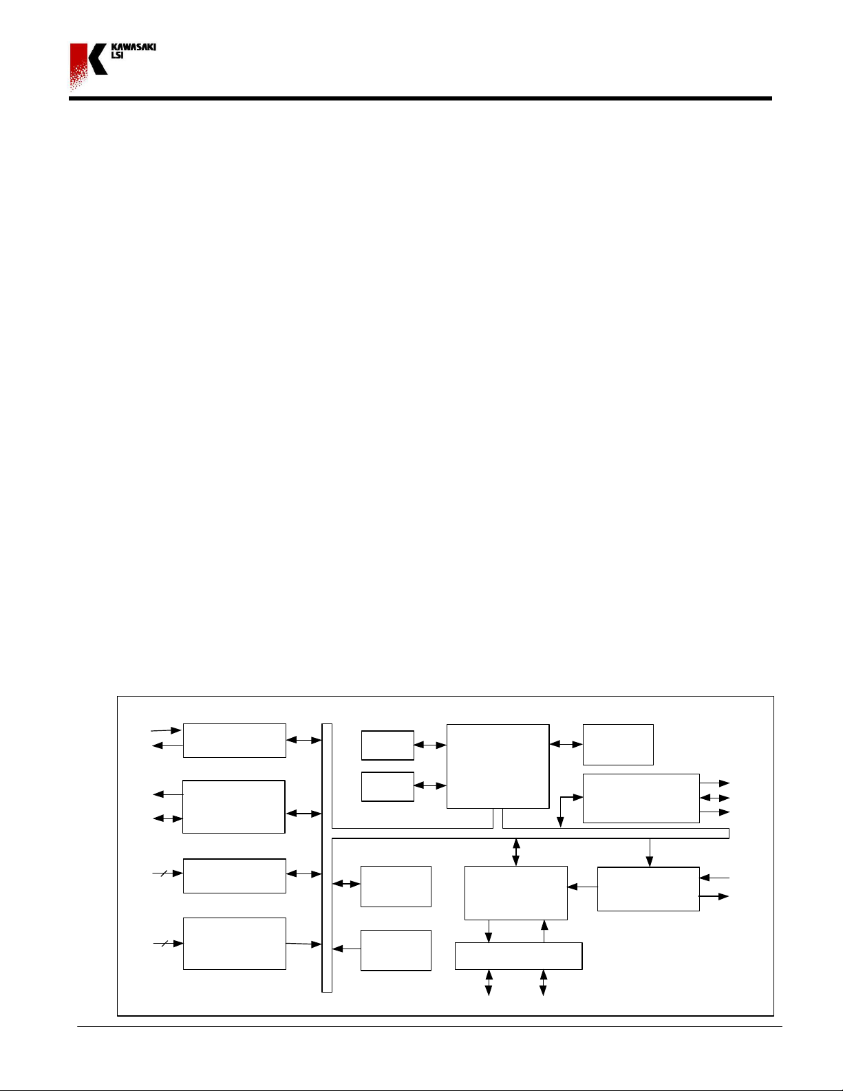
The Kawasaki KL5KUSB111 Controller is a unique single chip solution developed to interface the Universal Serial
Bus (USB) to HomePNA-Networks and standard 10base-T Networks. The KL5KUSB111 has been specifically
designed to provide a simple solution to communicate with Home Networking Applications at 1 Mb/s and/or 10 Mb/s
Ethernet. By utilizing the Kawasaki's USB to Ethernet technology that has been used throughout the industry. The
USB controller consists of a central 16-bit processor, mask ROM, RAM buffer, clock generator, HomePNA /
Ethernet interface, UART, IRQ, Watchdog Timer, Serial interface, External Memory Interface and Debug UART.
The SIE (Serial Interface Engine) is fully compatible with the USB specification. The Kawasaki USB to HomePNA
controller enables the advantages of Home Networking such as Shared Internet access, Printer/peripheral
sharing, File and application sharing and Networked gaming.
Features
• Advanced 16 Bit processor for USB transaction
processing and control data processing
• USB interface ver. 1.0/1.1 compliant
• Integrated Transceivers and SIE (Serial Interface
Engine)
• Internal Clock Generation
• Utilizes low cost external crystal circuitry
• 1.5K x 16 Internal RAM buffer
• Serial Interface for external EEPROM
Block Diagram
EEPROM
Serial Interface
• HomePNA compliant for 1Mb/sec.
• Fully IEEE 802.3 compliant 10 Mbit/sec
Ethernet MAC Layer. Interfaces serially of
an external ENDEC PHY.
• Debug UART
• External memory interface
• Compatible with most HomePNA PHY's
• Watchdog timer
• 100 pin LQFP package
Watchdog
16 Bit
Processor
Timer
Kawasaki LSI • 2570 North First Street • Suite 301 • San Jose, CA 95131 • Tel: (408) 570-0555 • Fax: (408) 570-0567 • www.klsi.com Ver. 2.3
1Mb/s PNA
and/or 10Mb/s
RAM
(3KB)
Mask ROM
(8KB)
Serial
Interface
Engine
PLL & Clock
Generator
1
KL5KUSB111
USB to HomePNA
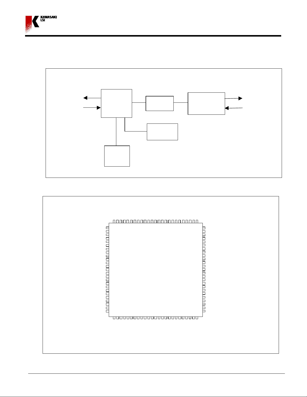
KL5KUSB111 Application Block Diagram
EEPROM
KL5KUSB111
Transformer
UVDD
N/C
N/C
PHRXCLK
RXD
IRQ0
IRQ1
DXA
FS
N/C
SERROMD
PU#1
PCLK
OGND
CLK
X2
XA_15
VDD
XA_7
1
USB
USB /
Ethernet
Optional
External
Memory
Pin Diagram 100LQFP
VDD
2
GND
VCO_IN
3
4
CP_OUT
PLLEN
5
6
N/C
N/C
7
8
N/C
N/C
9
10
N/C
N/C
11
12
VDD
GND
13
14
PHTXD0
PHCOL
15
16
PHTXEN
N/C
17
18
N/C
N/C
19
20
N/C
N/C
21
22
TXD
UGND
23
24
VP
VM
25
PHY
Serial
VDD
XD_15
XD_14
OGND
XD_13
XD_12
IGND
XD_11
XD_10
XD_9
XD_8
XD_7
XD_6
XD_5
XD_4
XD_3
XD_2
XD_1
XD_0
XA_13
9998979695949392919089888786858483828180797877
100
XA_12
KL5KUSB111_L
XA_11
XA_10
XA_9
XA_8
76
75
XA_6
74
73
XA_5
XA_4
72
71
XA_3
XA_2
70
69
XA_1
nTST
68
67
nRESET
nXROMSEL
66
65
nXWR
nXRD
64
63
GND
nPDN
62
61
N/C
N/C
60
59
N/C
N/C
58
57
LED_ON
nXRAMSEL
56
55
IGND
nXBHE
54
53
XA_0
XA_14
52
51
OVDD
Home
Network Phy
or/and
Full duplex
10 Base – T
Ethernet
Kawasaki LSI • 2570 North First Street • Suite 301 • San Jose, CA 95131 • Tel: (408) 570-0555 • Fax: (408) 570-0567 • www.klsi.com Ver. 2.3
26272829303132333435363738394041424344454647484950
PHCRS
PHTCLK
X_PCLK
PH_RXD0
TSCA
DRA
SERROMCLK
2
KL5KUSB111
USB to HomePNA
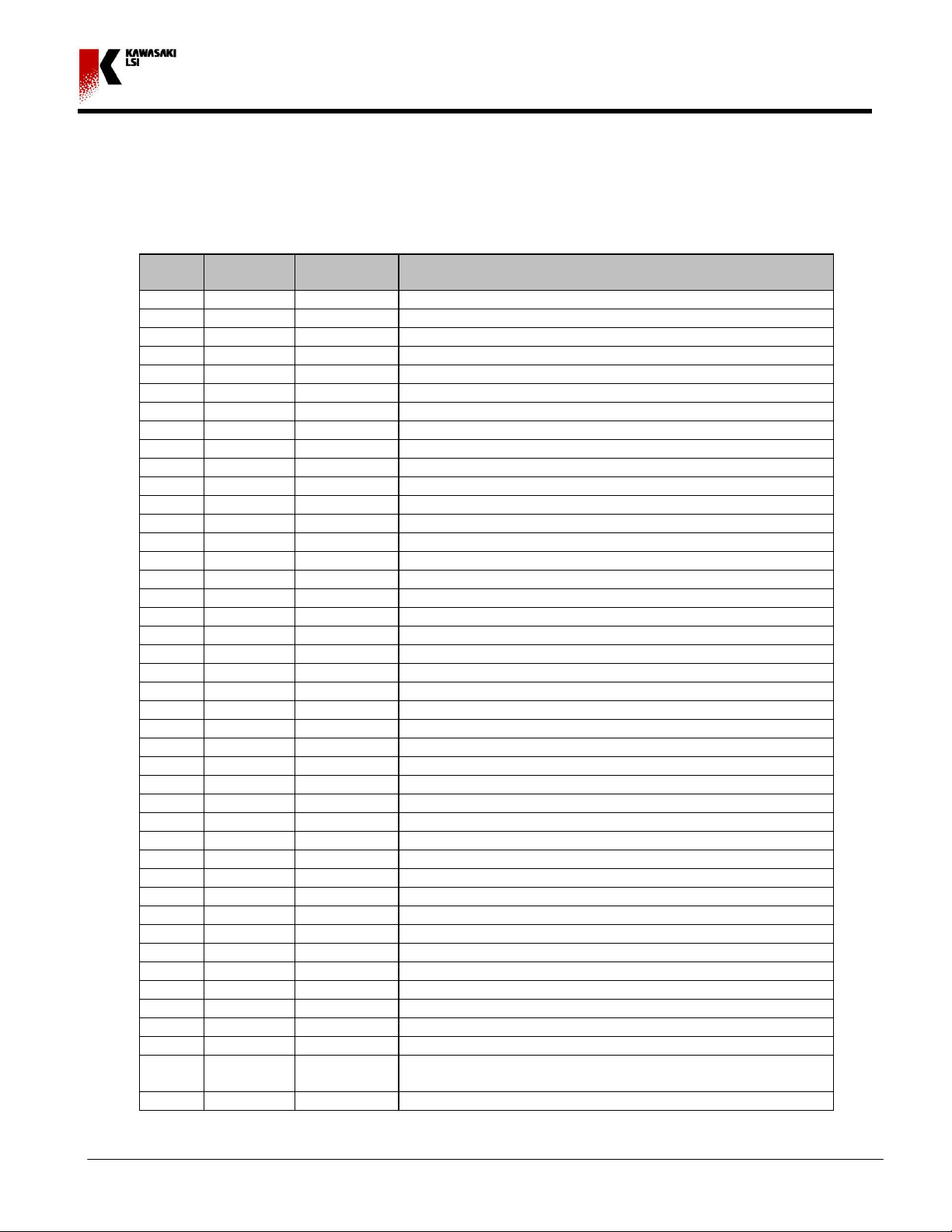
Pin Description
Pin #
LQFP
1 IN 0VDD VDD
2 IN GND GND
3 IN VCO_IN PLL VCO IN
4 OUT CP_OUT PLL VCO OUT
5 IN PLLEN PLL Enable
6 NC NC NC
7 NC NC NC
8 NC NC NC
9 NC NC NC
10 NC NC NC
11 NC NC NC
12 IN VDD VDD
13 IN GND GND
14 OUT PHTXD0 Transmit data to PHY
15 IN PHCOL Collision input from PHY
16 OUT PHTXEN Transmit Enable to PHY
17 NC NC NC
18 NC NC NC
19 NC NC NC
20 NC NC NC
21 NC NC NC
22 IN/OUT TXD UART TXD
23 IN UGND USB GND
24 IN/OUT VP USB+ Pin
25 IN/OUT VM USB- Pin
26 IN UVDD USB VDD
27 NC NC NC
28 NC NC NC
29 IN PHTXCLK PHY Transmit Clock
30 IN PHRXCLK PHY Receive Clock
31 IN PHCRS PHY Carrier Sense
32 IN PH_RXD0 PHY Serial Receive Data
33 IN/OUT X_PCLK External PCLK
34 IN/OUT RXD UART RXD
35 IN IRQ0 IRQ or GPIO10
36 IN IRQ1 IRQ or GPIO11
37 OUT DXA Sport Mode or GPIO7
38 IN TSCA Sport Mode or GPIO8
39 IN/OUT FS Sport Mode or GPIO9
40 NC NC NC
41 IN/OUT SERROMD Serial ROM data
42 OUT SERROMCLKSerial ROM clk
I/O Pin Name Description
43 IN/OUT PU#1 Pull up to USB + Pin for High Speed
Kawasaki LSI • 2570 North First Street • Suite 301 • San Jose, CA 95131 • Tel: (408) 570-0555 • Fax: (408) 570-0567 • www.klsi.com Ver. 2.3
3
 Loading...