

Kawasaki LSI KL5KUSB107 Datasheet
KL5KUSB107
1
Ver. 1.8
USB Combo - Serial & Parallel
Serial
PLL & Clock
16 Bit Address / Data Bus
16 Bit
Serial
Engine
RAM
EEPROM
Interface
VP
VM
CLK
X2
SCL
SDA
Watchdog
Timer
host
Txd
DTR
DCD
Txd
CTS
Channel 1
Channel 2
UART
IEEE1284
buffers
peripheral
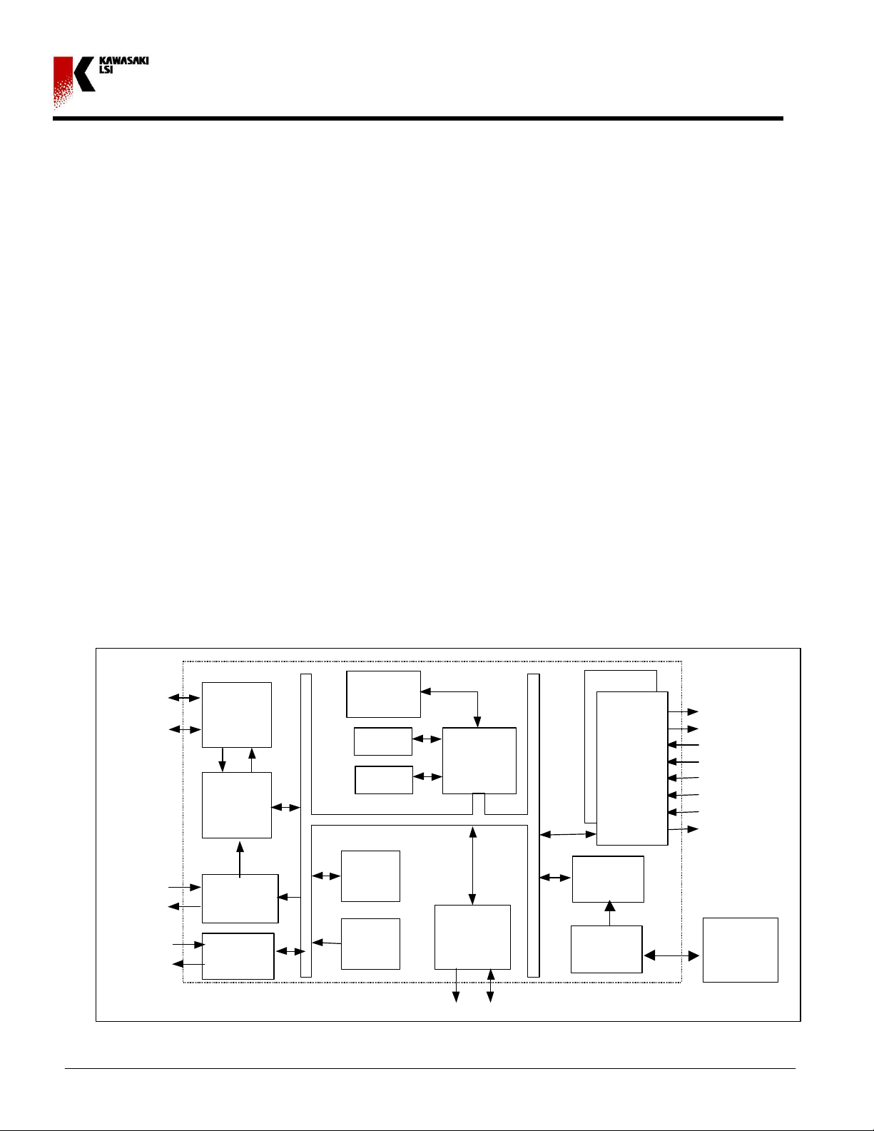
Description
The Kawasaki USB to Parallel / 2Serial enables your system to have the capability to communicate
between the USB (Universal Serial Bus) port and parallel port and 2 serial ports. This device meets the
USB 1.0/1.1 and IEEE1284 enhanced parallel port and standard serial port specifications. All the
advantages of USB are available to peripherals with parallel and serial port interface. With Kawasaki’s
USB to Serial/Parallel device and software, it is transparent to the peripheral and no firmware changes
are required which makes it possible to convert peripherals with serial and parallel interfaces to USB
interface with minimum modifications. This device is ideal for Legacy solutions.
Features
• Advanced 16 Bit processor for USB transaction
processing and control data processing
• Compliant with the USB 1.0/1.1 (Universal
Serial Bus)
• Plug and Play compatible
• Compliant with USB printer device class
specification
• Utilizes low cost external crystal circuitry
• IEEE1284 compliant including EPP and ECP
• PC parallel port register-based standard
operation
• 5V tolerate Centronics inputs pins.
Block Diagram
USB
Interface
Interface
• 2 serial ports
• 230Kbps serial baud rate
• 128 byte FIFO
• Serial EEPROM interface
• Utilizes low cost external crystal circuitry
• 1.5K x 16 internal RAM buffer for fast
communications
• Debug UART for debug and code development
• USB host device drivers available
• Multiple logical channels support
• Single-chip solution in a 100 pin LQFP
RTS
Interface
Processor
Serial
Interface
DSR
RI
Rxd
(3KB)
Generator
Mask
Debug
Rxd
Kawasaki LSI • 2570 North First Street • Suite 301 • San Jose, CA 95131 • Tel: (408) 570-0555 • Fax: (408) 570-0567 • www.klsi.com
ROM
Serial
IEEE1284
IEEE1284
parallel port
KL5KUSB107
2
Ver. 1.8
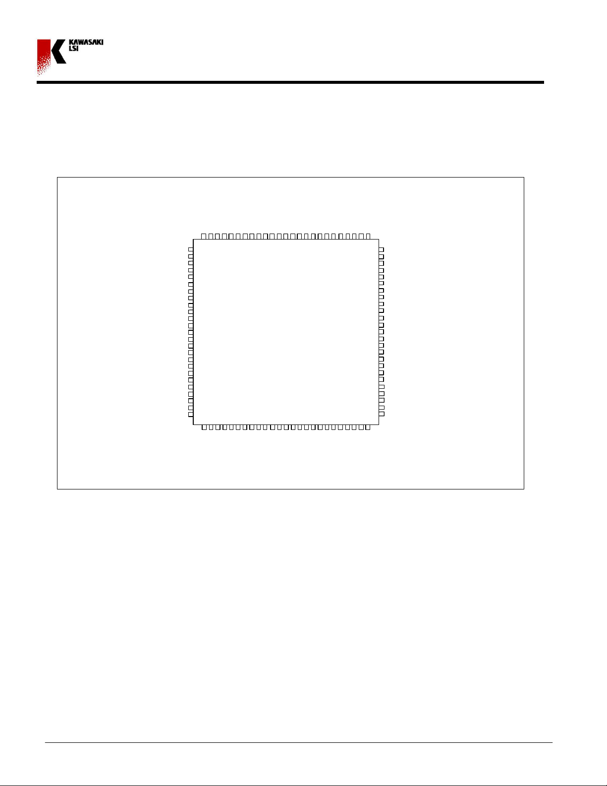
Pin Diagram 100LQFP
1
KL5KUSB107
PLLEN
nRXD
UART2_DTR
UART2_DSR
VDD
VDD
100
VDD
2
SDA
3
PU#1
4
PD7
5
PD6
6
PD5
7
PD4
8
PD3
9
PD2
10
PD1
11
PD0
12
PLH
13
GND
nTXD
GND
VP
VM
14
15
16
17
18
19
20
21
22
23
24
25
UART1_Txd
UART1_Rxd
UART1_RTS
UART1_DTR
UART1_CTS
UART1_DSR
UART1_DCD
UART1_RI
XD_15
XD_14
GND
XD_13
XD_12
XD_11
XD_10
XD_9
XD_8
XD_7
XD_6
XD_5
XD_4
XD_3
XD_2
XD_1
XD_0
GND
XA_13
XA_12
XA_11
9998979695949392919089888786858483828180797877
XA_10
100 LQFP
USB Combo - Serial & Parallel
XA_9
XA_8
76
75
XA_7
XA_6
74
73
XA_5
XA_4
72
71
XA_3
XA_2
70
69
XA_1
GND
68
67
nNTST
nNRESET
66
65
nXROMSEL
nXWR
64
63
nXRD
PE
62
61
BUSY
nFAULT
60
59
nINIT
nSLCTIN
58
57
nAUTOFEED
nXRAMSEL
56
55
GND
nXBHE
54
53
XA_0
XA_14
52
51
VDD
26272829303132333435363738394041424344454647484950
SCL
VDD
SELECT
GND
VCO_IN
VDD
CP_OUT
nACK
nPWR_DWN
UART2_Txd
UART2_Rxd
UART2_RTS
UART2_CTS
UART2_DCD
CLK
GND
nSTROBE
UART2_RI
X2
XA_15
Kawasaki LSI • 2570 North First Street • Suite 301 • San Jose, CA 95131 • Tel: (408) 570-0555 • Fax: (408) 570-0567 • www.klsi.com
KL5KUSB107
3
Ver. 1.8
Pin Description
USB Combo - Serial & Parallel
Pin #
LQFP
1 VDD VDD
2 IN/OUT SDA* Serial EEPROM serial data. Connect to EEPROM/SDA for
3 IN PU#1* Pull up to USB +Pin for High Speed
4 IN/OUT PD7 Parallel port: Data7
5 IN/OUT PD6 Parallel port: Data6
6 IN/OUT PD5 Parallel port: Data5
7 IN/OUT PD4 Parallel port: Data4
8 IN/OUT PD3 Parallel port: Data3
9 IN/OUT PD2 Parallel port: Data2
10 IN/OUT PD1 Parallel port: Data1
11 IN/OUT PD0 Parallel port: Data0
12 IN PLH* Parallel port: Peripheral Logic High
13 GND GND
14 OUT UART1_Txd* UART1: Transmit Data
15 IN UART1_Rxd* UART1: Receive Data
16 OUT UART1_RTS* UART1: Request To Send
17 OUT UART1_DTR* UART1: Data Terminal Ready
18 IN UART1_CTS* UART1: Clear To Send
19 IN UART1_DSR* UART1: Data Set Ready
20 IN UART1_DCD* UART1: Data Carrier Detect
21 IN UART1_RI* UART1: Ring Indicate
22 OUT nTXD Debug UART Txd
23 GND USB GND
24 IN/OUT VP USB DATA + Pin
25 IN/OUT VM USB DATA - Pin
26 VDD USB VDD
27 IN SELECT Parallel port: Printer is selected and online
28 OUT SCL* Serial EEPROM clock. Connect to EEPROM/SCL for
29 GND GND
30 IN VCO_IN PLL VCO In
31 OUT CP_OUT PLL VCO Out
32 VDD VDD
33 IN PLLEN* PLL Enable
34 IN nRXD* Debug UART Rxd
35 IN nACK Parallel port: Acknowledge
36 OUT nPWR_DWN Power Down
37 OUT UART2_Txd* UART2: Transmit Data
38 IN UART2_Rxd* UART2: Receive Data
39 OUT UART2_RTS* UART2: Request To Send
40 OUT UART2_DTR* UART2: Data Terminal Ready
41 IN UART2_CTS* UART2: Clear To Send
42 IN UART2_DSR* UART2: Data Set Ready
43 IN UART2_DCD* UART2: Data Carrier Detect
I/O Pin Name Description
<=16Kb EEPROM, and EEPROM/SCL for >16Kb EEPROM
<=16Kb EEPROM, and EEPROM/SDA for >16Kb EEPROM
Kawasaki LSI • 2570 North First Street • Suite 301 • San Jose, CA 95131 • Tel: (408) 570-0555 • Fax: (408) 570-0567 • www.klsi.com
 Loading...