

Kawasaki LSI KE5BLME008 Datasheet

Version 1.0.1 Proprietary and Confidential
Longest Match Engine
KE5BLME008
Kawasaki LSI U.S.A., Inc.

Version 1.0.1 Proprietary and Confidential
Table of Contents
1. Features ..........................................................................................................................1
Block Diagram................................................................................................................2
3. Pin Assignment and Description ....................................................................................3
3.1. Pin Assignment: Diagram...........................................................................................3
3.2. Pin Assignment: List .................................................................................................4
3.3. Pin Descriptions .........................................................................................................6
4. Functional Descriptions .................................................................................................8
4.1. Overview...................................................................................................................8
4.2. Reset .........................................................................................................................8
4.3. Initialization ..............................................................................................................9
4.4. Data Insertion............................................................................................................9
4.5. Search .......................................................................................................................9
4.6. Data Deletion...........................................................................................................12
4.7. Search via CPU Port................................................................................................12
4.8. Interruption..............................................................................................................12
4.9. Typical Operational Flow ........................................................................................13
5. DRAM...........................................................................................................................17
5.1. DRAM Specification...............................................................................................17
5.2. Connecting to DRAM..............................................................................................17
6. Register.........................................................................................................................18
6.1. Register Map...........................................................................................................18
6.2. Register Description ................................................................................................18
7. Command Description .................................................................................................21
8. Package Outline............................................................................................................27
9. Electrical Characteristics.............................................................................................28
9.1. Absolute Maximum Rating......................................................................................28
9.2. Operating Conditions...............................................................................................28
9.3. DC Characteristics...................................................................................................28
9.4. AC Characteristics...................................................................................................29
Kawasaki LSI
8K Longest Match Search Engine (KE5BLME008) PRELIMINARY
Version1.0.1 Proprietary and Confidential
1
1. Features
The KE5BLME008 provides the best solution to a high-speed route search with the following
functions:
•
The device can store 8,192-route prefixes.
•
Maximum Clock Frequency: 66 MHz.
•
•
•
Maximum 4.1 Mpps (packet per sec. at 66MHz clock)
•
330 ns (hit flag; match length output)
420 ns (associative data output)
•
•
CPU port: 16 bit
Input port: 32 bit
Output port: 16 bit
•
16Mbit EDO DRAM
•
•
LVTTL
•
Single 3.3V ± 0.3V Supply
•
LQFP 176 Pin Package
•
Kawasaki LSI
8K Longest Match Search Engine (KE5BLME008) PRELIMINARY
Version1.0.1 Proprietary and Confidential
2
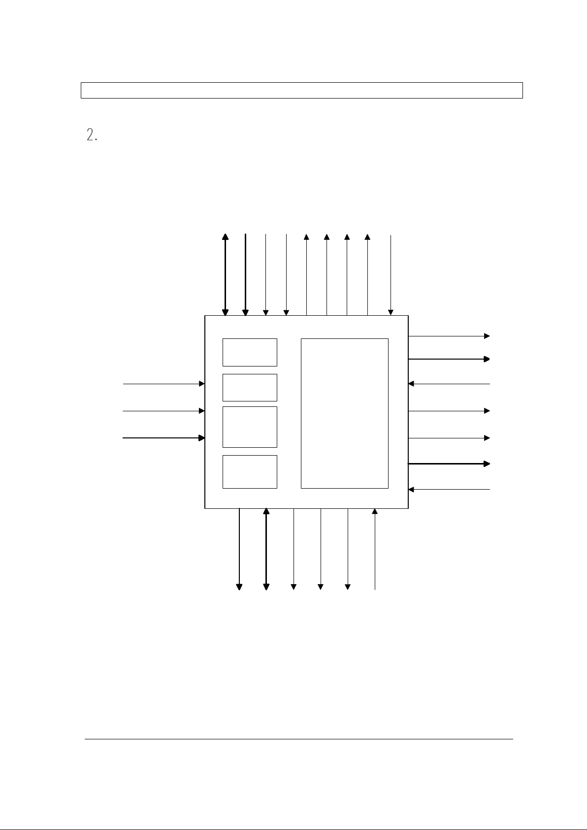
Block Diagram
Fig. 2.1 Block Diagram
DAT[15 : 0]
ADD[3 : 0]
CEN
RWN
RSTN
IRQN
OUT[15 : 0]
MDONEN
HON
OEN
FLN
AMFLN
MLE[4 : 0]
CLK
SRCHN
SDAT[3 1 :0]
CCMPN
DADD[9 :0]
DDAT[15 : 0]
DWEN
DRAS
DCAS
Registers
Search Table
8k Entries
Ins / Del
Queue
DRAM
Control
Control
Logic
CPU
Port
DRAM
Port
Input
Port
Output
Port
MLOEN
DRI
ODONEN

Kawasaki LSI
8K Longest Match Search Engine (KE5BLME008) PRELIMINARY
Version1.0.1 Proprietary and Confidential
3
3. Pin Assignment and Description
3.1. Pin Assignment: Diagram
Fig. 3.1 Pin Assignment
44
1
INDEX
132 89
176
133
45
88
•• •••• ••
•• •••• ••
•• •••• ••
•• •••• ••
Kawasaki LSI
8K Longest Match Search Engine (KE5BLME008) PRELIMINARY
Version1.0.1 Proprietary and Confidential
4
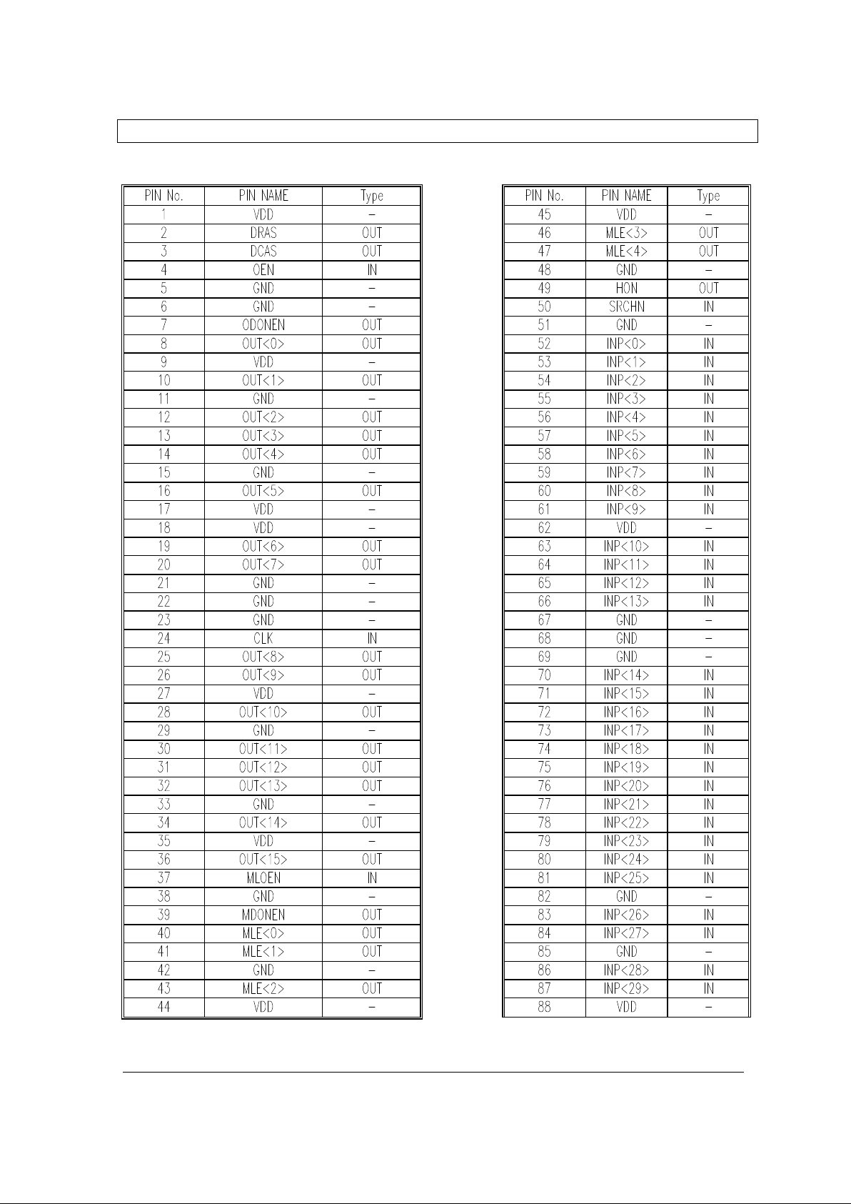
3.2. Pin Assignment: List
Table 3.1 Pin Assignment
Kawasaki LSI
8K Longest Match Search Engine (KE5BLME008) PRELIMINARY
Version1.0.1 Proprietary and Confidential
5
Table 3.1 Pin Assignment (cont’d)

Kawasaki LSI
8K Longest Match Search Engine (KE5BLME008) PRELIMINARY
Version1.0.1 Proprietary and Confidential
6
3.3. Pin Description
Pin Name Attribute Description # of Pins
CLK Clock
Input
LVTTL
CLK is the master clock input. Input
signals refer to the rising edge of CLK.
1
SRCHN Search Enable
Input
LVTTL
SRCHN enables a search operation;
search commences when Low is
signaled.
1
INP<31:0> Input Bus
Input
LVTTL
INP<31:0> is a 32-bit input bus used
for search key inputs.
32
OUT<15:0> Output Bus
Output
LVTTL
OUT<15:0>, a 16-bit output bus,
outputs the associate data.
16
OEN Output Enable
Input
LVTTL
OEN controls OUT<15:0>. OEN Low
enables OUT<15:0> ; and OEN High
enables High-Z.
1
ODONEN Output DONE
Output
LVTTL
ODONEN Low Active indicates that
the associate data is output to the OUT
<15:0> after a search.
1
HON Hit Output
Output
LVTTL
HON outputs a search result.
Low indicates a hit; High indicates a
miss hit.
1
MLE<4:0> Match Length
Output
LVTTL
MLE outputs match-length
information (prefix lengh-1) between
the data stored in the table and the
relevant search key.
5
MLOEN Match Length Output Enable
Input
LVTTL
MLOEN controls MLE<4:0> Output
Enable. Low enables MLE<4:0>;
High changes it to High-Z.
1
MDONEN MLE Done
Output
LVTTL
MDONEN Low indicates that the
completion of the search, outputting
the match length to MLE<4:0>.
1
RSTN Reset
Input
LVTTL
RSTN input Low resets the hardware. 1
IRQN Interrupt Request
Output
Open Drain
IRQN indicates Low when an interrupt
condition occurs in the CNTL register.
1
CCMPN Command Execution
Completion
Output
LVTTL
CCMPN signals High during the
command operation executed via CPU
port, and signals Low upon the
completion of its execution.
1

Kawasaki LSI
8K Longest Match Search Engine (KE5BLME008) PRELIMINARY
Version1.0.1 Proprietary and Confidential
7
Pin Name Attribute Description # of Pins
ADD<3:0> CPU Port Address
Input
LVTTL
ADD<3:0> is a register address. 4
DAT<15:0> CPU Port Data Bus
Input
LVTTL
DAT<15:0> is an input/output data bus
for a CPU port.
16
CEN CPU Port Enable
Input
LVTTL
CEN serves as the CPU port access; CEN
Low enables the input operations of data
and command.
1
RWN Read/Write
Input
LVTTL
RWN determines the direction of the CPU
bus; RWN Low selects “write” cycle, and
RWN High “read” cycle.
1
FLN Full
Output
LVTTL
FLN outputs Low when all entries are
filled with valid data.
1
AMFLN Almost Full
Output
LVTTL
AMFLN outputs Low when reaching
“almost full”; the number of entries is
equal to or exceeds the value stored in the
Almost Full Register.
1
DADD <9:0> DRAM Address
Output
LVTTL
DADD outputs DRAM address. Ensure
that it is connected to the DRAM address
pins.
10
DDAT <15:0> DRAM Data
Input/Output
LVTTL
DDAT <15:0> is a bi-directional data bus
to DRAM. Ensure that it is connected to
the DRAM data input/output.
16
DWEN DRAM Write Enable
Output
LVTTL
DWEN is a DRAM Write Enable signal.
Ensure that it is connected to the DRAM
Write enable input.
1
DRAS DRAM RAS
Output
LVTTL
DRAS is a row address select signal to the
DRAM. Ensure that it is connected to the
RAS pin of DRAM.
1
DCAS DRAM CAS
Output
LVTTL
DCAS is a column address select signal to
the DRAM. Ensure that it is connected to
the relevant CAS pin of DRAM.
1
DRI RAS Timing Input
Input
LVTTL
RAS Timing Input controls DRAM
timing. Ensure that it is connected to the
DRAS pin.
1
VDD Supply The voltage required is 3.3V. 21
GND Ground Ground pin. 38

Kawasaki LSI
8K Longest Match Search Engine (KE5BLME008) PRELIMINARY
Version1.0.1 Proprietary and Confidential
8
4. Functional Descriptions
4.1. Overview
KL5BLME008 is a search device for 32-bit IP address searches in IP routing applications. Its
capability extends beyond a simple lookup of data entries stored in a routing table. With its
compatibility with the CIDR (Classless Inter-Domain Routing), it outputs associated data for
the longest match data when there are multiple matching entries. KE5BLME008 also has the
search capability of finding the exact 32-bit match for searching the host address.
Moreover, LME008 provides a solution to routes having the same address with different
prefix length. Let us assume, for instance, the presence of both 192.1.0.0/16 and 192.1.0.0/24
in a routing table; the search key of 192.1.1.2 outputs associated data relative to 192.1.0.0/16
whereas the search key of 192.1.0.3 outputs ones relative to 192.1.0.0/24.
KL5BLME008 is a triple-port architecture equipped with task-specific ports: Input port
conducting a search, Output port effecting a result, and CPU port executing commands and
accessing to a register. This triple-port architecture facilities insertion and deletions of entries
without interrupting a search operation.
In order to store data, LME008 operates with an external 16Mbit EDO DRAM. Memory
control operations such as DRAM accesses and Refresh are, however, controlled by the
device itself.
4.2. Reset
The LME008 device requires a reset after chip power up. A reset can be applied by either
supplying a low pulse to the RSTN pins or writing any data onto a Reset register. The values
reassigned for both pins and registers are as follows:
Registers Pins
CNTL: 0000b IRQN: High-Z
STAT0: 1x00b FLN: High
STAT1: 0000b AMFLN: High
PR0 – RR2: Unknown CCMPN: Low
Almost Full Address: 0FFFh ODONEN: High
Refresh Counter Constant: 000001b (01h) MDONEN: High
HON: High
DWEN: High
DOEN: High
DRAS: High
DCAS: High

Kawasaki LSI
8K Longest Match Search Engine (KE5BLME008) PRELIMINARY
Version1.0.1 Proprietary and Confidential
9
4.3. Initialization
After resetting the device, execute the Initialize command, which is required for data to be
properly inserted into the device. The execution of this command requires approximately
7.8µs at 66MHz clock. Before proceeding with the subsequent commands, check anew by
monitoring the CCMPN pin whether the initialization process has been completed.
4.4. Data Insertion
To enter data in the table, use the Insert command. Ensure that the IP address is set to WR01, the associated data to WR2, and PL (prefix length –1) to WR4.
Example:
When inserting 192.1.2.0/24 with associated data 3456h, enter the following.
WR0: 0200h (2.0)
WR1: C001h (192.1)
WR2: 3456h
WR4: 0017h (23 = 24–1)
Ensure that the value entered in WR4 is the prefix-length minus 1, not the prefix-length
itself.
The completion of the Insert command is confirmed by a low signal on the CCMPN pin.
Proceed with the subsequent commands after checking the CCMPN status.
LME008 is capable of storing the exact data match, i.e., the entry data hitting only when all
the 32 bits coincide with the input key data. When inserting exact match data, set 31 to WR4
(PL). This particular function is useful for storing the host address in the table.
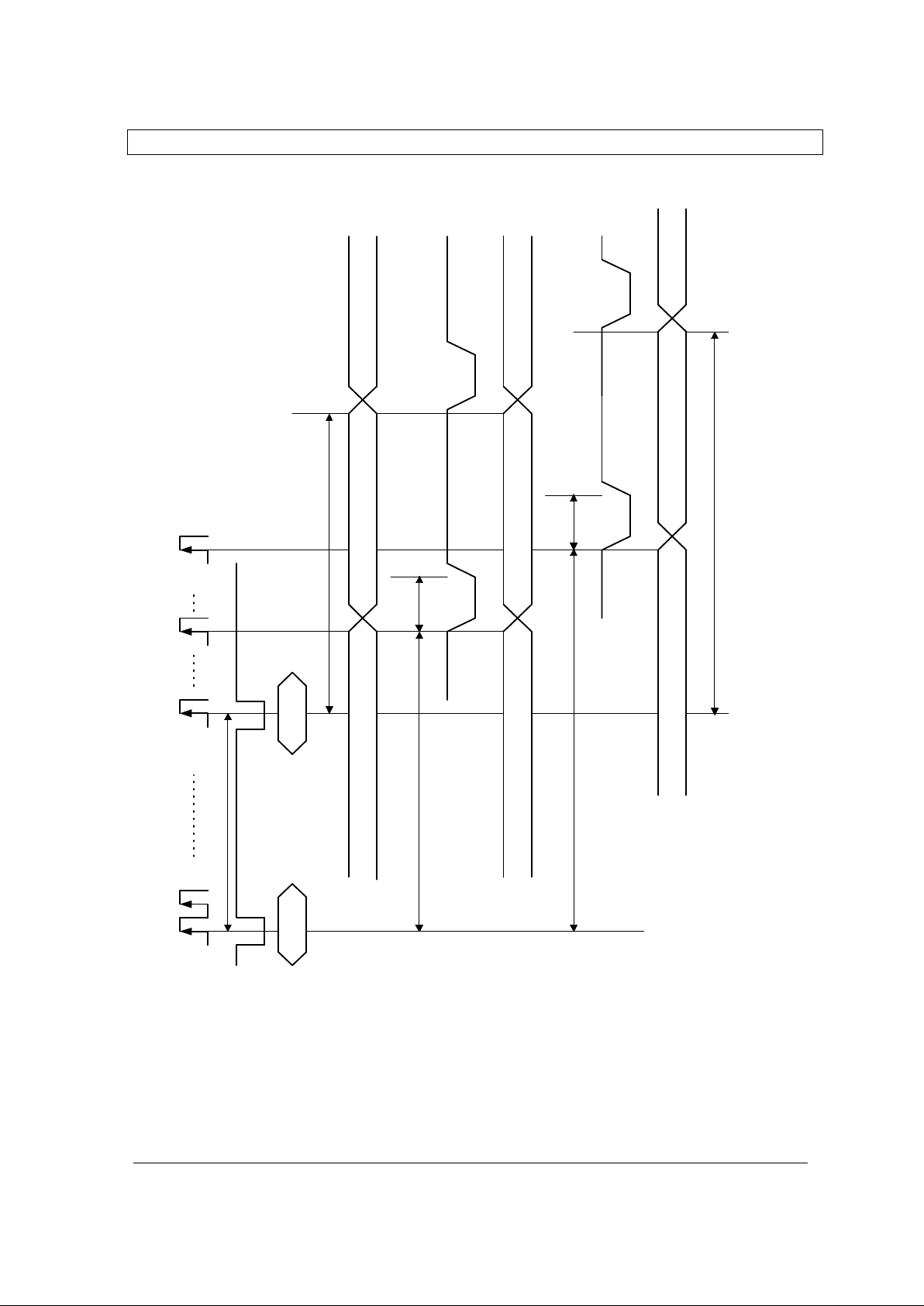
4.5. Search
To conduct a longest match search, apply data to INP [31:0], and set a SRCHN pin Low (see
Fig.4.1). At the 22nd clock after starting a search, MDONEN will be changed to Low,
allowing both MLE [4:0] and HON to output. MLE [4:0] output should be equal to the match
length minus one. That is to say, MLE [4:0] is the maximum value of the match length of a
search key minus 1. The HON status indicates a lookup result, with Low a hit, and High as a
miss hit. MDONEN will revert from High to Low after 4 clock cycles, while both MLE [4:0]
and HON will be held until the next lookup result.
At the 28th clock after starting a search, ODONEN will be changed into Low, allowing OUT
[15:0] to output associated data. If the search results in a miss match, the value pre-registered
at the default associated data will be returned. ODONEN will revert from High to Low after
4 clock cycles, whereas OUT [15:0] will be held until the next result. For instance, let us
assume the presence of the following data in the table:
Kawasaki LSI
8K Longest Match Search Engine (KE5BLME008) PRELIMINARY
Version1.0.1 Proprietary and Confidential
10
133.5.0.0/16 [associated data: 1111h]
133.5.16.0/24 [associated data: 2222h]
Cf. Default associated data: 0000h
The result is as follows:
Search Key Result HON status MLE[4:0] OUT[15:0]
133.5.16.2 Hit at
133.5.16.0/24
Low 23 (17h) 2222h
133.5.17.3 Hit at
133.5.0.0/16
Low 15 (0fh) 1111h
133.6.0.1 Miss hit* High 0 0000h
Note: “*” indicates that133.5.0.0 and 133.6.0.1 have the matching length of 14-bits; a
miss hit occurs because the matching length is shorter than the registered value of
“16.”
Kawasaki LSI
8K Longest Match Search Engine (KE5BLME008) PRELIMINARY
Version1.0.1 Proprietary and Confidential
11
CLK
SRCHN
INP<31:0>
HON
MDONEN
MLE<4:0>
ODONEN
OUT<15:0>
28 Clocks
4 Clocks
Key1 Key2
Search result of Key 1
Search result of Key 1
Search result of Key 1
Search result of Key 2
Search result of Key 2
Search result of Key 2
16 Clocks min.
4 Clocks
22 Clocks
22 Clocks
28 Clocks
Fig. 4.1 Search Timing

Kawasaki LSI
8K Longest Match Search Engine (KE5BLME008) PRELIMINARY
Version1.0.1 Proprietary and Confidential
12
4.6. Data Deletion
To delete data from the table, use the Delete command. Ensure that the IP address is set to
WR0-1, and PL to WR4 with a prefix-length minus 1 before executing the commands.
Example:
If deleting 192.1.2.0/24, set the registers as follows.
WR0: 0200h (2.0)
WR1: C001h (192.1)
WR4: 0017h (23 = 24–1)
Notes:
l Ensure that the value set to WR4 is the prefix-length minus 1, not the prefix-length
itself.
l No deletion can be performed if the value entered to WR4 differs from that of the
initial entry. For instance, if 0018h is entered to WR4 followed by the Delete
command execution, 192.1.2.0/24 will not be deleted and will remain in the table.
The completion of the Delete command will be confirmed by a low status of CCMPN pin.
Before proceeding with the subsequent commands, check anew to confirm that the Delete
command execution has finished.
4.7. Search via CPU Port
A search can be performed with the CPU port commands, independently of the Input port
operation. Apply a search key data to WR0-1 to execute the Search command. Upon
completion of a table lookup, associated data will be written to RR0; and both ML (prefixlength minus one) and hit-or-miss-hit information will be written to RR2. The command
execution can be confirmed by monitoring the CCPN pin status; before proceeding with
subsequent commands, ensure that the CCMPN pin is changed to Low.
4.8. Interruption
To conduct interruption or a series thereof, set a CNTL register. Interruption is not
accomplished unless one of the conditions is met, as described in “6.2. Register
Description.” For instance, setting both bit 2 and bit 0 of a CNTL register to “1” activates
the Interrupt operation upon completion of either the Initialize command or the table
fulfillment process. To clear Interrupt, read STAT1, which should revert each bit to “0.”

Kawasaki LSI
8K Longest Match Search Engine (KE5BLME008) PRELIMINARY
Version1.0.1 Proprietary and Confidential
13
Notes:
l The Interrupt operation set to the bit 3 occurs ONLY after the executions of
Search/Insert/Delete commands. No other commands are valid.
l The Interrupt operation set to the bit 2 occurs ONLY after the execution of the
Initialize command. No other commands are valid.
l The Interrupt operation set to the bit 1 occurs ONLY after the execution of either
the Insert or Delete command when the values registered in the Entry Count match
those of the Almost Full Register. See the example below:
Example: Entry Count = 999 (3E7h)/Almost Full Register = 1000 (3E8h)
Command Entry Count Interruption AMFLN
Insert 1000 Generated Low
â
Insert 1001 Not generated Low
â
Insert 1002 Not generated Low
â
Delete 1001 Not generated Low
â
Delete 1000 Generated Low
â
Delete 999 Not generated High
l The Interrupt operation set to the bit 0 occurs ONLY after the table becomes full.
4.9. Typical Operational Flow
(1) Turn on the power.
(2) Reset
Input a Low pulse to a RSTN.
(3) Initialize.
Write “Initialize” (0004h) onto the COM register (00h).
Wait for CCMPN to turn to Low.
(4) Set a Refresh Counter:
(a) Write 001Dh onto the WR0 (04h).
(b) Write the Set Refresh Counter Constant (06h) onto the COM register (00h).
(c) Wait for CCMPN to turn to Low.
Note: In case of 66MHz, Refresh Cycle Time will be (31+1) * 484.8ns
=15.51µs.
 Loading...