

Kawasaki LSI KE5BGCA128BCFP, KE5BGCA128ACFP Datasheet

Preliminary
Ver. 1.2.2
GigabitCAM
KE5BGCA128

Preliminary
GigabitCAM KE5BGCA128
1. Features
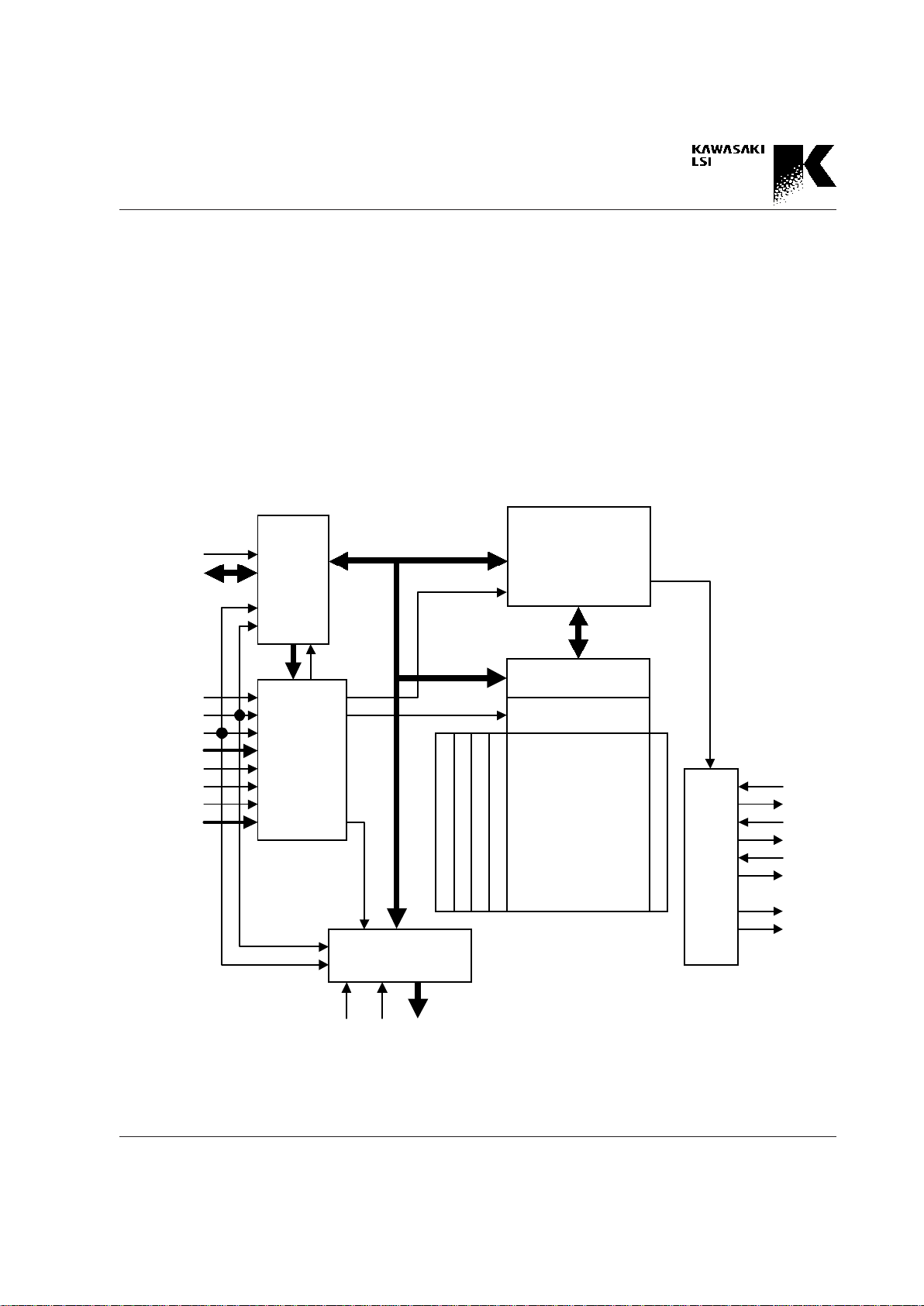
2. Block Diagram
3. Pin Assignment and Pin Descriptions
3.1 Pin Assignment
3.2 Pin Descriptions
4. Functional Descriptions
4.1 Access from CPU Port
4.2 Read/Write Registers
4.3 Access to the CAM Memory
4.4 Search
4.5 Data Management by Commands
4.6 Restriction in Pipeline Operation
4.7 Latency
5. Connection
5.1 Initialization
5.2 Single Device Operation
5.3 Cascade Connection
5.3.1 Device ID Registration
5.3.2 Priority
5.3.3 CPU Port in a Cascaded
System
5.3.4 Output Port in a Cascaded
System
6. Command Descriptions
6.1 Command Functions
6.2 Command Format
7. Register Descriptions
7.1 Overview
7.2 Register Addresses
7.3 Register Bit Maps
7.4 Conditions for Accessing Registers
8. Package Information
8.1 Ordering Information
8.2 Package Drawing
9. Electrical Characteristics
9.1 Absolute Maximum Rating
9.2 Operating Range
9.3 DC Characteristics
9.4 AC Characteristics
Contents

1-1
Preliminary
GigabitCAM KE5BGCA128
1. Features
The KE5BGCA128 provides best solution to the fast "Address Filtering" requirements of today's internetworking
switching equipment with the following outstanding
functions.
• 128k-bit capacity of table
- 64-bit x 2048 entries
- CAM/RAM substitution
• Dual Port Architecture
- 32-bit I/O Port
- 16-bit Output Port
• 12 Search Conditions
-12 Mask registers selected by the external pins
(MS<3:0>) and the CNTL1 register
- Access bit can be set for data aging
- Permanent bit can be set for permanent entry
- Automatic output of the contents of the Hit entry and
the Empty entry address from the 16-bit Output Port
• Cascading
- Table size is expandable.
- A cascaded table acts as one integral search data table
by internal device priority control.
• Commands
- Useful commands for table management such as aging
and purging.
- Useful command for Source Address Learning
• Synchronous Operation
- 30ns cycle time
- 64-bit input/30ns
- Search, data read/write, and command operations
are executed at high speed.
• 128-pin SQFP Package
• 3.3 v CMOS technology
2-1
Preliminary
GigabitCAM KE5BGCA128
64-bit x 2048
CAM
CNTL1/2 Registers
Memory R/W Registers
SCONF Register
CMP1/2 Registers
HHA/HEA Registers
MASK Register 0~11
Search Logic
Control Logic
Empty Bit
Permanent Bit
Access Bit
Priority Encoder
Decoder
Flag
Logic
DAT<31:0>
CLK
PHASE
PHIN
PHON
PMIN
PMON
FLIN
FLON
OEDATN
Output Port Control
OD<20:0>
SHON
SMON
OEODN
OPSL
SRCHN
RWN
CEN
RSTN
ADD<5:0>
MS<3:0>
CPU
Bus
Control
Pipeline
Execution
Control
Fig. 2 Block Diagram
2. Block Diagram
This device consists of the following blocks as shown.
CPU Bus Control Block
An access to the search key data, commands, or internal registers are executed through the CPU Bus.
Pipeline Execution Control
This block controls the pipeline operation of this device.
CNTL1/2 Registers
These registers define the mask registers and the input
modes , etc.

2-2
Preliminary
GigabitCAM KE5BGCA128
Memory R/W Registers
These registers are used to access the CAM table.
SCONF Register
This register defines the configuration of the search operation.
CMP1/2 Registers
These two registers store the search key data and both are
64 bits in width.
HHA/HEA Registers
These two registers respectively store the hit address and
the empty address of the CAM table.
MASK Registers
These 12 registers are used to mask the data bit by bit in
the search operation or the write operation to the CAM
table.
CAM
The capacity of the CAM table is 64 bits x 2048 entries.
Flag Logic
This block outputs the search result and the status of the
CAM table and has the interface function for a cascade
connection.
Output Port Control
This block controls the Output Port which outputs the
search result.
3-1
Preliminary
GigabitCAM KE5BGCA128
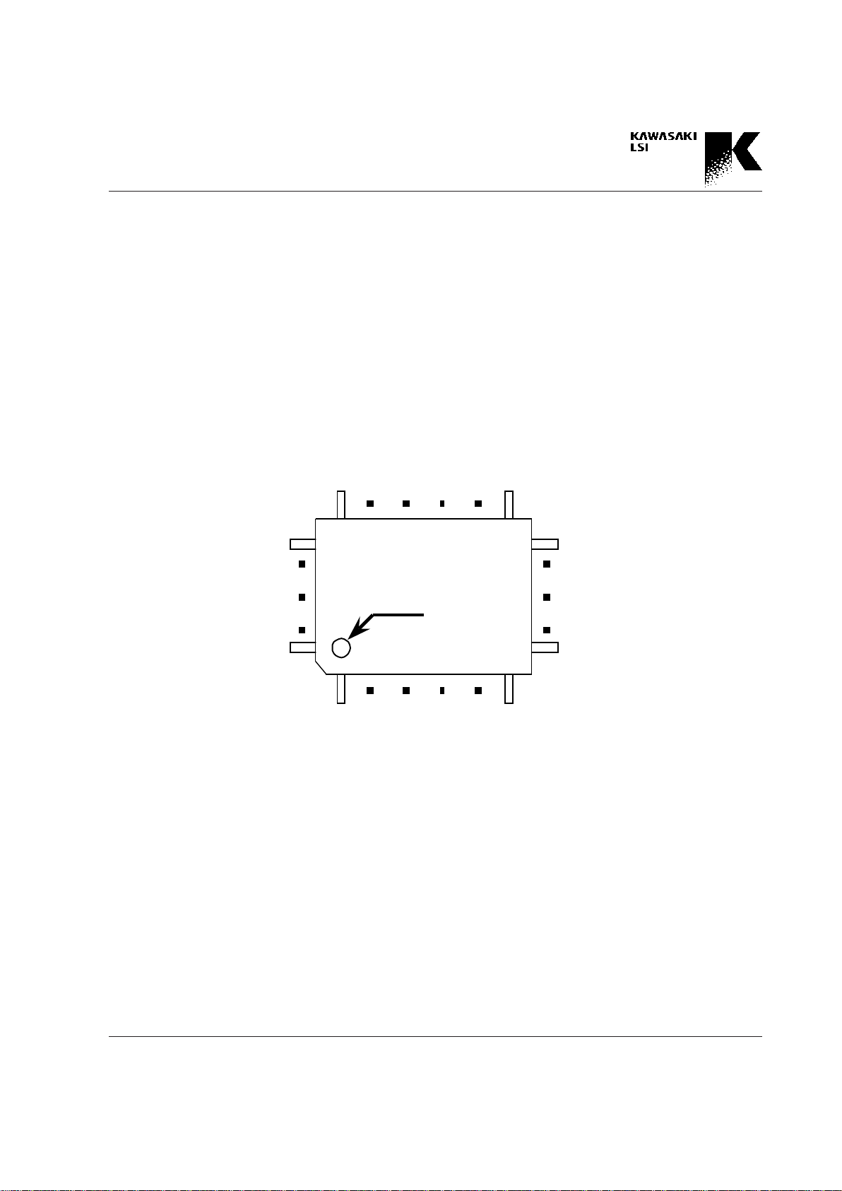
38
39
1
128
103
65
64
102
Index
KE5BGCA128
3. Pin Assignment and Pin Descriptions
3.1 Pin Assignment
KE5BGCA128
(128pin SQFP type)
Fig. 3.1.1 Pin Assignment
3-2
Preliminary
GigabitCAM KE5BGCA128
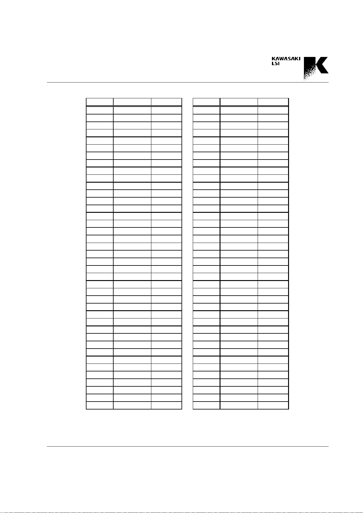
Pin No. Signal Name I/O type Pin No. Signal Name I/O type
1 GND - 41 GND 2 OD<0> OUT 42 PMON OUT
3 OD<1> OUT 43 PHON OUT
4VDD - 44FLININ
5VDD - 45PMININ
6 OD<2> OUT 46 PHIN IN
7 OD<3> OUT 47 VDD 8OD<4>OUT 48OPSL IN
9GND - 49OEODNIN
10 OD<5> OUT 50 GND 11 OD<6> OUT 51 GND 12 OD<7> OUT 52 GND 13 GND - 53 MS<0> IN
14 OD<8> OUT 54 MS<1> IN
15 VDD - 55 MS<2> IN
16 OD<9> OUT 56 MS<3> IN
17 OD<10> OUT 57 DA T<0> I/O
18 GND - 58 DA T<1> I/O
19 GND - 59 VDD 20 GND - 60 DA T<2> I/O
21 OD<11> OUT 61 DA T<3> I/O
22 VDD - 62 GND 23 OD<12> OUT 63 DA T<4> I/O
24 VDD - 64 DA T<5> I/O
25 OD<13> OUT 65 GND 26 OD<14> OUT 66 DA T<6> I/O
27 GND - 67 DA T<7> I/O
28 OD<15> OUT 68 VDD 29 OD<16> OUT 69 VDD 30 OD<17> OUT 70 DA T<8> I/O
31 OD<18> OUT 71 DA T<9> I/O
32 GND - 72 GND 33 OD<19> OUT 73 DAT<10> I/O
34 VDD - 74 DA T<11> I/O
35 VDD - 75 DA T<12> I/O
36 OD<20> OUT 76 GND 37 GND - 77 DA T<13> I/O
38 FLON OUT 78 VDD 39 SMON OUT 79 DAT<14> I/O
40 SHON OUT 80 VDD -
Table.3.1 Pin Assignment
3-3
Preliminary
GigabitCAM KE5BGCA128
Pin No. Signal Name I/O type Pin No. Signal Name I/O type
81 PHASE IN 121 CEN IN
82 CLK IN 122 RW N IN
83 GND - 123 SRCHN IN
84 GND - 124 OEDATN IN
85 GND - 125 NC OP EN* 1
86 DAT<15> I/O 126 GND 87 DAT<16> I/O 127 GND 88 VDD - 128 GND 89 DAT<17> I/O
90 DAT<18> I/O *1 NC pins must be open. (Do not connect.)
91 DAT<19> I/O
92 GND 93 DAT<20> I/O
94 DAT<21> I/O
95 DAT<22> I/O
96 GND 97 DAT<23> I/O
98 VDD -
99 VDD 100 DAT<24> I/O
101 DAT<25> I/O
102 G ND 103 DAT<26> I/O
104 DAT<27> I/O
105 G ND 106 DAT<28> I/O
107 DAT<29> I/O
108 DAT<30> I/O
109 DAT<31> I/O
110 V DD 111 AD D<0> IN
112 AD D<1> IN
113 AD D<2> IN
114 AD D<3> IN
115 G ND 116 G ND 117 G ND 118 AD D<4> IN
119 AD D<5> IN
120 RSTN IN
Table 3.1 Pin Assignment (cont'd)

3-4
Preliminary
GigabitCAM KE5BGCA128
3.2 Pin Descriptions
Pin name Attr ibute Function
CLK
CLOCK
Input
LVTTL
CLK is the master clock input. Other i nput si gnals are ref er r ed to the
rising edge of CLK.
PHASE determines the act ion timing of the device. The latency of the
output is also determined by the relationship between PHASE and
CLK.
PHASE
PH A SE
Input
L VTTL
Regardless of wh ether the input mode i s 32 bits ( Normal Access
Mode) or 64 bits (Fir st Access Mode), two cycles of the CL K signals
are necessary. P HASE reg ul ate s the input timing of the data input
from 32-bit DAT<31:0> when the input m ode i s 64 bits.
When PHASE is high, the data on DAT<31:0> is input in the 32 bits
on the MSB side of 64 bits. When PHASE is low,
the data is input in the 32 bits on the LSB side. When the input mode
is 32 bits, the 32-bit data is written in the register designated by
ADD <5 :0> on t he rising ed ge of CLK whil e P HASE i s low.
DAT<31:0>
CPU Bus
Input/Output
Tristate LVTTL
DATA<31 :0> is a 32- bi t, bidir ectional data bus used to convey data,
to ex ecute com m ands, and to write/read to and f r om the regi sters. The
direction is controlled by RWN and there is latency when the bu s is
switched.
ADD<5:0>
CP U Bu s Addre ss Bus
Input
L V TTL
ADD< 5: 0 > i s a 6-bi t address bus used to sel ect r egi sters.
CEN
Device E n able
Input
L VTTL
CEN is used to access the CP U port. The active CEN enabl es the
i nput oper ati on of data and command.
RWN
Read /Write
Input
L VTTL
RWN i s used to deter mine the direction of the CP U bus. RWN lo w
selects a write cycle, and RWN high selects a read cycle. There is
latency between the RWN change and the output as the result of the
data bus change.
OEDATN
CPU Bus Output Enable
Input
LVTTL
OEDATN controls the CPU bus output. OEDATN low enables the
output of the CPU bus by the read operati on, and O ED ATN hi gh
make s th e C PU bu s ha ve high i mpeda nc e desp it e t he out pu t
indication by the read operation. There is latency between the
OED ATN change and i ts resul t.
SRCHN
Search Enable
Input
LVTTL
SRCHN enables the search operation together with the write
operation to t he comparand register.

3-5
Preliminary
GigabitCAM KE5BGCA128
Pin name Attr ibute Function
MS<3:0>
Mask Select
Input
LVTTL
MS<3 :0> is a m ask select signal . One of 12 Mask regi sters is selected
by the MS<3:0>.
RSTN
Hardware Reset
Input
LVTTL
R S T N is used to reset the hardwa r e.
OD<20:0>
Output Port
Output
Tristate LVTTL
OD <20:0> is a 21-bit output po rt. T he de v ice ID is outpu t in the 5 bits,
OD<20:16> from the MSB, and HHA, HE A, or MEMHHA is output i n
the 16 bits from the LSB.
OEODN
Output Port Output Enab le
Input
LVTTL
OEODN control s th e Output Port. OEODN low enable s the output ,
and OEODN high disables the output (i.e. the Output Port is made
high impedance). There is latency between the OEODN change and
its result.
OPSL
Ou t put Port Select
Input
L VTTL
OPSL low enables the out put of MEMHHA from the Output Port.
There is latency between the OPSL change and its result.
SHON
Synchronous Hit Output
Output
LVTTL
SHON output s the search results in the device syn chronous with the
master clock. This pin is low when even one hit occurs i n the sear ch
operati on. This pin is high when no entry is hi t.
SMON
Synchronous Multi-hit Output
Output
LVTTL
SMON outputs the search results in the device synchr onous with the
master clock . This pin is low w hen mu l ti- hi t occurs in the search
operation. This pin is high when no multi-hit occurs.
PHON
Priority H it Output
Output
LVTTL
PHON outputs the search results. This pin is not synchronous with
the master cl ock. This pin is low when even one hit occur s in the
search operation. This pin is high when no entry is hit.
In a cascaded system, the hit signal of the cascade configuration
appears in the P HON pi n of the lowest prior ity device (Last Device).
PMON
Prio rity Multi- h it O utput
Output
L VTTL
PMON outputs the search results. This pin is not synchronous wi th
the master cl ock. This pin is low when m ul ti-hit occurs i n the sear ch
operation. This pin is high when no multi-hit occurs.
In a cascaded system, the mu lti-hit signal of the cascade
confi gurati on appears in the PMO N pi n of the lowest prior ity device
(Last Device).

3-6
Preliminary
GigabitCAM KE5BGCA128
Pin name Attribute Function
PHIN
Priority Hit Inpu t
Input
LVTTL
PHIN is used to connect plural devices in a cascaded system.
PMIN
Priorit y Mult i- h it Inp ut
Input
L V TTL
PMIN is used to connect plural devices in a cascaded system.
FLON
Full Fla g Ou tput
Output
L V TTL
FLON outputs the search results. This pin is low wh en all entries in
the CAM are fi l led with valid entri es (ful l status) and ther e i s
no mor e entry for a new regi stration. In a cascaded system, the full
signal of the cascade configurati on appear s in the F LON pin of the
lowest priority device (Last Device).
FLIN
Full Fla g I nput
Input
L V TTL
FLIN is used in a cascaded system.
VDD Suppl y
Power supply : 3.3V±0.3V
GND (Supply) Ground
Ground
4-1
Preliminary
GigabitCAM KE5BGCA128
4. Functional Descriptions
4. 1 Access from CPU Port
This device has a 32-bit data bus as a CPU port. Data read/
write is performed by the registers that are mapped with 32bit width (Refer to Chapter 7.2). To access registers wider
than 32 bits or to access the CAM memory, two data read/
write accesses are required. A special high speed write
mode (Fast Write Mode) is provided for the data write.
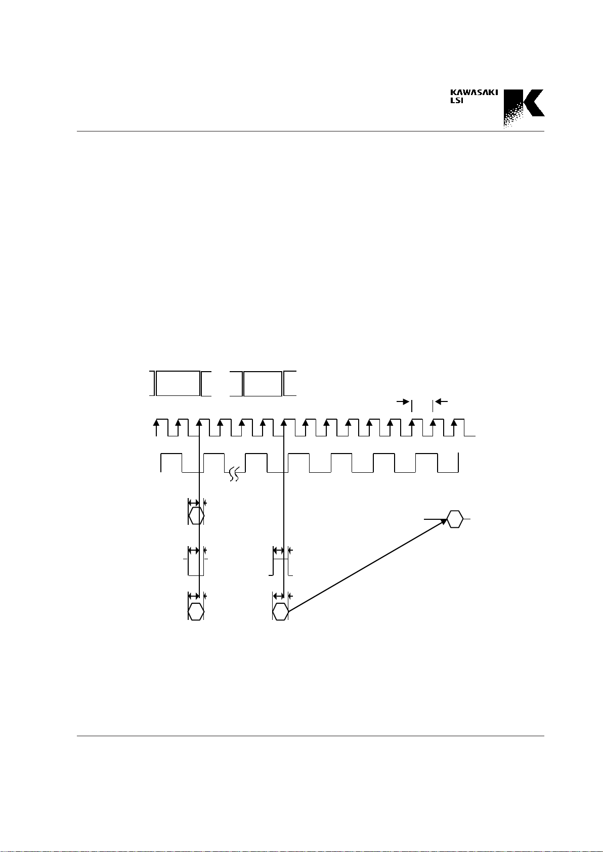
• Normal Access Mode
In this mode, one 32-bit data read/write is done with one
PHASE signal cycle. Data, address and control signals must
be input synchronously with the rising edge of CLK when
the PHASE signal, which is a double cycle signal of the
CLK, is low. (See Fig. 4.1.1 (a))
All the bits of each register address are valid in this mode.
Each 32-bit register is defined by the address pins
ADD<5:0>. Two accesses cycles are required for the read/
write of 64-bit registers and the CAM memory.
DAT<31:0>
CLK
PHASE
RWN
ADD<5:0>,CEN
MS<3:0>, SRCHN
Setup Hold
Setup Hold
Setup Hold
Setup Hold
Setup Hold
Data write
(32bits)
Data read
(32bits)
Input
Operation
DAT read Latency=4
<63:32>
or
<31:0>
<63:32>
<31:0>
or
min. 15ns
Fig. 4.1.1 (a) CPU Access Mode (Normal Access Mode)
4-2
Preliminary
GigabitCAM KE5BGCA128
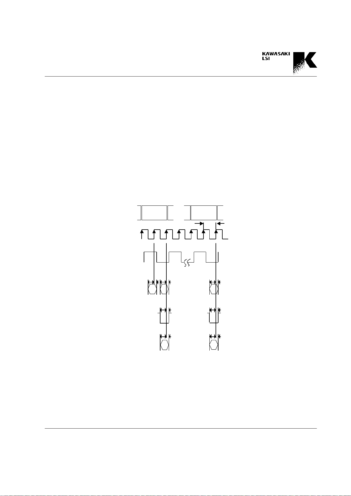
• Fast Write Mode
In this mode, one 64-bit data read/write is done within one
PHASE signal cycle. The upper 32-bit data of the 64-bit register is input synchronously with the rising edge of CLK
when the PHASE signal, which is a double cycle signal of
the CLK, is high. The lower 32-bit data of the 64-bit register,
address, and control signals are input synchronously with
the rising edge of the CLK signal when the PHASE signal is
low. (See Fig. 4.1.1 (b)) The LSB of the address is ignored in
this case. If a 32-bit register is accessed in this mode, only
the data, the address, and the control signals that are input
with the rising edge of CLK while the PHASE signal is low,
are valid. (See Fig. 4.1.1 (b)) The LSB of the address is also
ignored in this case.
Normal Access or Fast Write Mode is selected by the definition of the CNTL1 register. The initial definition after the
device reset is Normal Access Mode.
Fig. 4.1.1 (b) CPU Access Mode (Fast Write Mode)
CLK
PHASE
DAT<31:0>
RWN
ADD<5:1>,CEN
MS<3:0>, SRCHN
Setup
Hold
Setup
Hold
Setup Hold
Setup
Hold
Setup Hold
Setup Hold
Data write
(64bits)
Data write
(32bits)
<63:32>
<31:0> <31:0>
min. 15ns
Operation
Input

4-3
Preliminary
GigabitCAM KE5BGCA128
Fig. 4.2.1 Data read/write Timing Chart (Fast Write Mode)
4.2 Read/Write Registers
The register address is designated by the address pins of
the CPU port, and the data is inputted on the DAT bus. (See
Fig. 4.2.1) The function of each register is described in Chapter 7. This figure shows the example of the Fast Write Mode.
In case of the Normal Access Mode, data write is the same
as the Fast Write Mode shown in Fig. 4.2.1 if you exclude
the write of the upper 32 bits of the 64-bit word.
CEN
CLK
PHASE
Data write
(64bits)
Input
Operation
RWN
MS<3:0>
SRCHN
ADD<5:0>
DAT<31:0>
Data write
(32bits)
Data read
(32bits)
Data read
(32bits)
Data write
(64bits)
Data read
(32bits)
Data read
(32bits)
WAIT
Data write
(32bits)
Data write
(32bits)
WAIT
min. 15ns
<63:32><31:0>
<31:0> <31:0> <63:32>
or<31:0>
<63:32>
or<31:0>
<31:0> <63:32>
or<31:0>
<31:0>
<63:32>
or<31:0>
*1)64bits data write *1)
DAT read Latency=4DAT read Latency=4
<63:32>
4-4
Preliminary
GigabitCAM KE5BGCA128
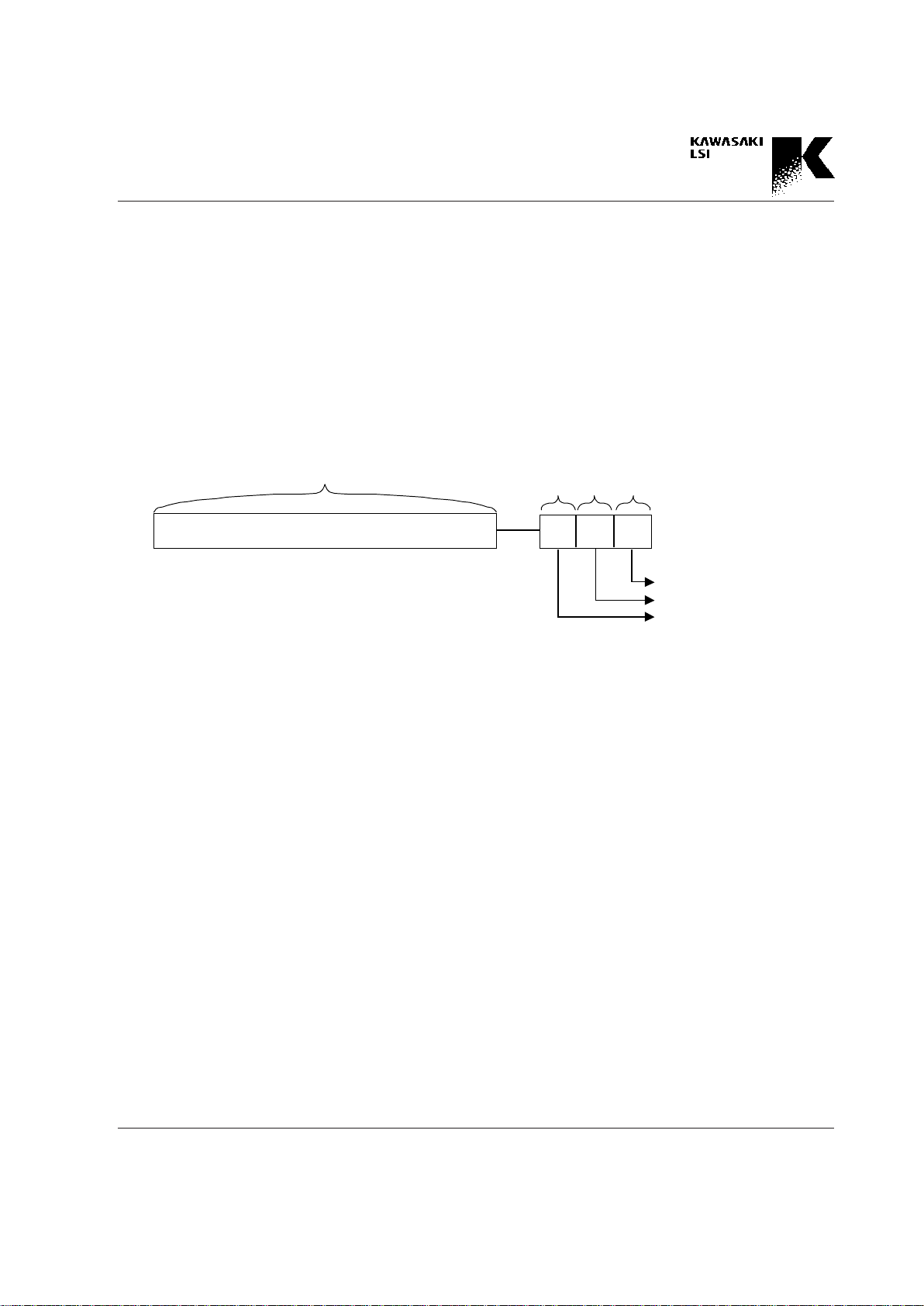
Fig.4.3.1 Word Structure of CAM
Permanent Bit
Access Bit
Empty Bit
Content
64 bits
1bit 1bit 1bit
4.3 Access to the CAM Memory
• Word Structure of CAM
One word of the CAM is made up of 64-bit CAM memory
and 3 attribute bits (1 bit each). The 64-bit CAM memory
stores the users data to be searched. The attribute bits are
the Empty Bit, the Permanent Bit, and the Access Bit.
(See Fig. 4.3.1):
The Empty Bit: The Empty Bit is a flag that indicates the
validity of the CAM word. An invalid word is excluded from
the search target and is recognized as a candidate for
memory for a new registration of valid data.
The flag logic is:
0 : valid (Valid data is written);
1 : invalid (Memory is a space).
The Permanent Bit: The entry whose Permanent Bit is set
to "1" will not become invalid (Empty Bit = 1) by any purge
commands. In order to clear this bit, users can use the reset
command.
The Access Bit: The Access Bit is provided for the management of the hit career of each entry. Users can specify
whether the hit career is held in the Access Bit or not for
each search cycle. Once the Access Bit is set to "1," however, it holds "1" until an Access Bit reset command is executed.
These attribute bits can be directly modified by accessing
the MEMAR_AT, MEMHHA_AT, and MEMHEA_AT
registers.
These bits are reset by the reset signal from the RSTN pin as
follows:
• The Empty Bit : 1 (Invalid)
• The Permanent Bit : 0 (Impermanent)
• The Access Bit : 0 (No hit career)

4-5
Preliminary
GigabitCAM KE5BGCA128
• Read/Write CAM Memory
Read/write of the entry data is executed not by direct address indication, but by indirect address indication through
specific registers (MEMAR, MEMARAI, MEMAR_AT,
MEMHHA, MEMHHA_AT, MEMHEA, MEMHEAAI, and
MEMHEA_AT). When writing through MEMAR,
MEMARAI, MEMHHA, MEMHEA, and MEMHEAAI, 12
kinds of mask conditions can be selected. Mask in the data
write operation means that the data of masked bit is not
changed by the write operation. There are two ways to select the mask condition from the 12 mask registers (MASK0
- MASK11). One way is to select it with 4 single pins,
MS<3:0> applied dynamically in data write. The other way
is to select by the definition in the CNTL1 register statically
.
The read/write of the CAM memory is basically the same as
the read/write of the registers. As shown in Fig. 4.2.1, the
mask condition in the write operation is selected by
MS<3:0>, the status of these select control signals is
latched by the rising edge of CLK while the PHASE signal is
low, and the data is written to the memory with Latency 2.
The read data is output from the CPU port with Latency 4.
(See Section 4.7 about Latency.)
• Read/Write CAM Data through the MEMAR
register
Read/write operation of the CAM word, whose address is
designated by the AR register, is executed by the MEMAR
register. Write through the MEMAR register changes the
attribute bits in the CAM word as follows:
• Empty Bit : 0 (Entry is valid.)
• Permanent Bit : Return to the default value defined
in the CNTL1 register
• Access Bit : Return to the default value defined in
the CNTL1 register.
•Read/Write CAM Data through the
MEMARAI register
Read/write operation of the CAM word, whose address is
designated by the AR register, is executed by the
MEMARAI register. One read/write to the MEMARAI register increments the value of the AR register automatically.
Write through the MEMARAI register changes the attribute bits in the CAM word as follows:
• Empty Bit : 0 (Entry is valid.)
• Permanent Bit : Return to the default value defined
in the CNTL1 register.
• Access Bit : Return to the default value defined in
the CNTL1 register.
•Read/Write CAM Data through the
MEMHHA register
Read/write operation of the CAM word, whose address is
designated by the HHA register, is executed by the
MEMHHA register. Read/write through the MEMHHA
register is prohibited when the address stored in the HHA
register is invalid, because this may cause an access to the
undesired CAM word and the data in it might be destroyed.
Read/write through the MEMHHA register does not
change the attribute bits in the CAM word.

4-6
Preliminary
GigabitCAM KE5BGCA128
•Read/Write CAM Data through the
MEMHEA register
Read/write operation of the CAM word, whose address is
designated by the HEA register, is executed by the
MEMHEA register. Read/write through the MEMHEA register is prohibited when the address stored in the HEA register is invalid, because this may cause an access to the
undesired CAM word and the data in it might be destroyed.
Write through the MEMHEA register changes the attribute
bits in the CAM word as follows:
• Empty Bit : 0 (Entry is valid.)
• Permanent Bit : Return to the default value defined
in the CNTL1 register.
• Access Bit : Return to the default value defined in
the CNTL1 register.
•Read/Write CAM Data through the
MEMHEAAI register
Read/write operation of the CAM word, whose address is
designated by the HEA register, is executed by the
MEMHEAAI register. One read/write to the MEMHEAAI
register shifts the value of the HEA register to the value of
the next HEA automatically. Write through the
MEMHEAAI register changes the attribute bits in the CAM
word as follows:
• Empty Bit : 0 (Entry is valid.)
• Permanent Bit : Return to the default value defined
in the CNTL1 register.
• Access Bit : Return to the default value defined in
the CNTL1 register.
•Read/Write CAM Data through the
MEMAR_AT, MEMHHA_AT, and
MEMHEA_AT registers
Read/Write operation to the attribute bits of the CAM word,
whose address is designated by the AR, the HHA, and the
HEA registers respectively, is executed by these registers.
Examples of this operation would be to make the designated
CAM word Invalid, to make the designated CAM word Permanent, and/or to change the Access bit of the designated
CAM word. Users can mask each attribute bit. (Refer to
Chapter 7 for more details.)
This capability also enables the attribute of the CAM word
to be read.
4-7
Preliminary
GigabitCAM KE5BGCA128
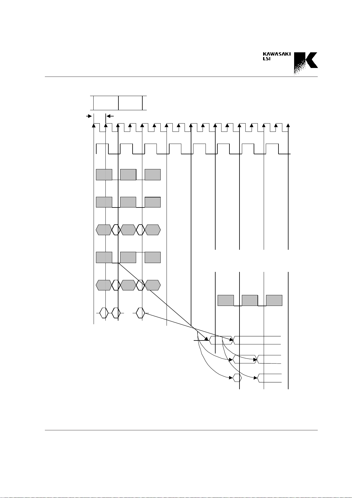
Fig. 4.4.1 SRCH Operation through CMP Register Write
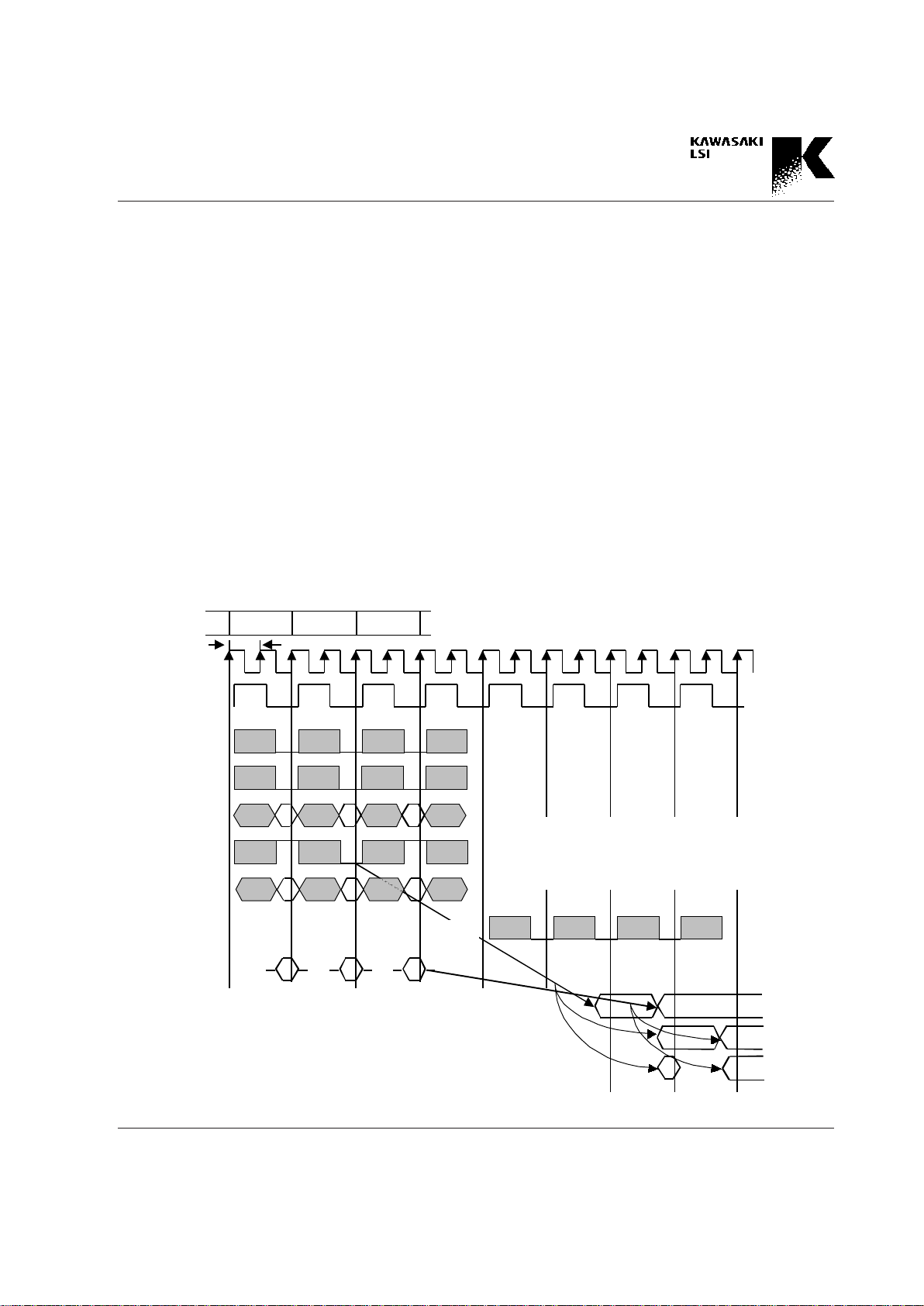
4.4 Search
• Search Operation through the CMP1/2 register
The key data should be written to the CMP1/2 register from
the CPU bus. The low pulse of the SRCHN pin synchronized with the rising edge of CLK while the PHASE signal is
low activates the search operation when the key data is
written. The mask condition for the search is also chosen
from 12 kinds of mask conditions defined by the MASK
registers (MASK0 - MASK11), dynamically by the status of
the MS<3:0> pins or statically by the CNTL1 register.
The CMP1/2 register stores the key data until the next write
operation is done. Users can choose to perform a Search
Operation in the Normal Access mode or the Fast Write
mode. The example is shown in Fig. 4.4.1 (a/b).
In Fig. 4.4.1, the search operation is started by the data write
to the CMP1/2 register and the synchronous low pulse to
the SRCHN pin. As a result, the Hit flag is output on the
SHON pin with Latency 4, the Multi-Hit flag is output on the
SMON pin with Latency 5, and the HHA and the DEVID of
the device which has a hit are output on the OD<20:0> with
Latency 5. Fig. 4.4.1 shows two methods for searching the
CAM. In this example, the first search is executed by a
pulse from the SRCHN pin using the data previously written
to the CMP1/2 register. The second search operation is executed by the command, SRCH 1/2. This time, the search
operation by command is executed with the data already
written in the CMP1/2 register used in the previous search.
CEN
CLK
PHASE
SRCH
RWN
MS<3:0>
SRCHN
ADD<5:0>
DAT<31:0>
Data write
(32bits)
min. 15ns
<31:0>
(or<63:32>)
<63:32>
(or<31:0>)
SHON
SMON
OD<20:0>
<31:0>
COM
(SRCH)
(a) Normal Access Mode
Operation
Input
Latency
SHON: 4 (or 5)
SMON: 5
OD (HHA, DEVID): 5 (or 6, 7, 4)
OEODN
4-8
Preliminary
GigabitCAM KE5BGCA128
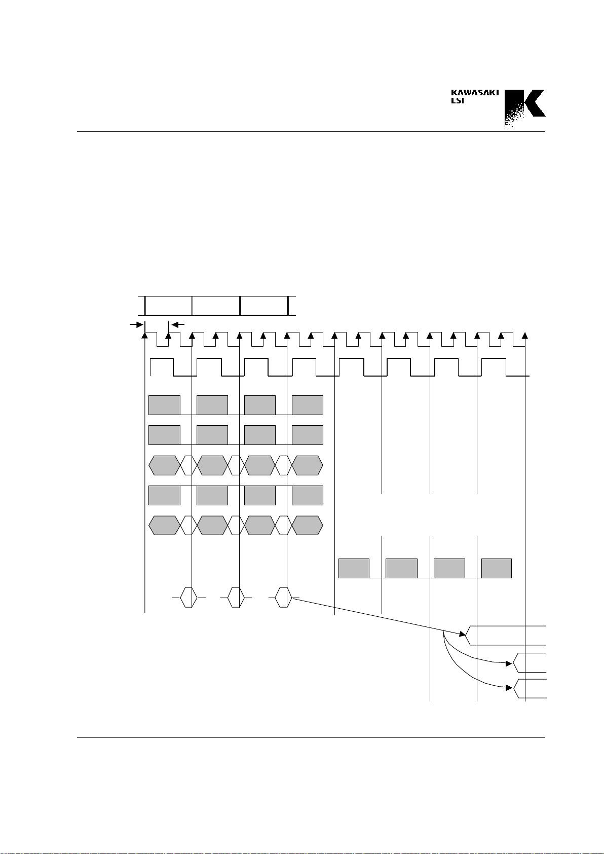
Fig. 4.4.1 SRCH Operation through CMP Register Write
CEN
CLK
PHASE
RWN
MS<3:0>
SRCHN
ADD<5:1>
DAT<31:0>
SRCH
<31:0> <31:0><63:32>
COM
(SRCH)
(b) Fast Write Mode
Operation
Input
min. 15ns
SHON
SMON
OD<20:0>
Latency
SHON: 4 (or 5)
SMON: 5
OD (HHA, DEVID): 5 (or 6, 7, 4)
OEODN
4-9
Preliminary
GigabitCAM KE5BGCA128
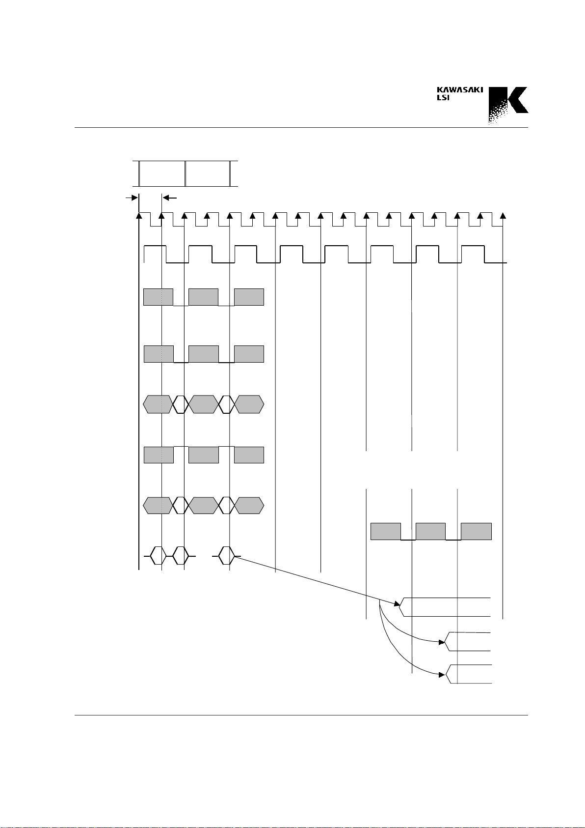
Fig. 4.4.2 SRCH Operation with COMMAND
• Search Operation by commands
The search command, SRCH 1/2, written to the command
register (COM register) activates the search operation using
the key data stored in the CMP1/2 register.
The mask condition for the search is chosen at the time of
command write from 12 kinds of mask conditions defined by
the MASK registers (MASK0 - MASK11). The mask register is chosen dynamically by the status of the MS<3:0> pins
on the rising edge of the CLK signal while the PHASE signal
is low or statically by the CNTL1 register. Like the search
operation above, users can choose the write mode from the
Normal Access mode or the Fast Write mode. In both
modes, the search operation is started by the command
(SRCH). The example is shown in Fig. 4.4.2 (a/b).
CEN
CLK
PHASE
Input
Operation
RWN
MS<3:0>
SRCHN
ADD<5:0>
DAT<31:0>
Data write
(32bits)
min. 15ns
<31:0>
(or<63:32>)
<63:32>
(or<31:0>)
<31:0>
COM
(SRCH)
(a) Normal Access Mode
Data write
(32bits)
SHON
SMON
OD<20:0>
Latency
SHON: 4 (or 5)
SMON: 5
OD (HHA, DEVID): 5 (or 6, 7, 4)
OEDON
4-10
Preliminary
GigabitCAM KE5BGCA128
Fig. 4.4.2 SRCH Operation with COMMAND
CEN
CLK
PHASE
Input
Operation
RWN
MS<3:0>
SRCHN
ADD<5:1>
DAT<31:0>
<31:0> <31:0><63:32>
SHON
SMON
OD<20:0>
COM
(SRCH)
(b) Fast Write Mode
Data write
(64bits)
min. 15ns
OEODN
Latency
SHON: 4 (or 5)
SMON: 5
OD (HHA, DEVID): 5 (or 6, 7, 4)

4-11
Preliminary
GigabitCAM KE5BGCA128
• Access Bit set while searching
When a hit occurs in the CAM word while searching, the hit
result of the entry can be stored as the Access Bit data.
This means the past career of the hit results can be managed. For every 12 MASK registers, the determination of
whether the search result is stored in the Access Bits or not
(whether the Access Bits must be set according to the hit
result) can be done using the SCONF register. (Refer to
Chapter 7 for more details.)
• Search Result
Flag pins (PHON, PMON, SHON, SMON)
The PHON and SHON pins indicate if the Hit word (the
CAM word which is hit) exists. A high level on the PHON
pin indicates that a single hit does not exist and a low level
on this pin indicates that a single hit exists and multi-hit
does not exist. A high level on the SHON pin indicates that
no hit exist and a low level on this pin indicates that a single
hit or Multi-Hit exist. The PHON pin goes to an unknown
status when the search operation starts, and it outputs high
or low level according to the search result. The PHON pin
outputs the search results asynchronously with the CLK.
The SHON outputs the corresponding search result synchronously with CLK. (See Fig. 4.4.2. Refer to Chapter 5 for
more details)
The PMON and SMON pins indicate if Multi-Hit entries
exist. A high level of these pins indicates that a multi-hit
does not exist and the low level of this pin indicates that a
multi-hit exists. The PMON and SMON pin goes to an unknown status when the search operation starts, and it outputs high or low level according to the search result The
PMON pin outputs the search results asynchronously with
the CLK. The SHON outputs the corresponding search result synchronously with CLK. (See Fig. 4.4.2.)
HHA register
The HHA register stores the address of the CAM word that
is hit by the search operation. The HHA register has the
valid bit that indicates the validity of the data stored in the
HHA register. This valid bit becomes “0” if single hit (no
multi-hit word exist) exists. If a multi-hit or no hit exists, the
valid bit becomes “1” , invalid. The HHA register also
stores the data output to the PHON and PMON pins according to the search result, namely Hit and Multi-Hit flag data
(Labeled SYH and SYM in section 7.3 Register Bit Maps). In
a cascaded system in which multiple devices are interconnected, the Last Device in the chain holds the Hit and MultiHit flags of the total system.
Careful consideration is required for the HHA register, because the HHA (Highest Hit Address) becomes invalid data
when a multi-hit exists. The search configuration register,
SCONF, allows the user to set the Access Bit according to
the search operation results. Even though a multi-hit is set
as invalid, all the Access Bits of Hit words are still set.
Hit and Multi-Hit status of the total system is valid only
when the HHA register in the Last Device is accessed with
the timing which considers the propagation delay between
the devices.
MEMHHA register
The MEMHHA register is used to read and write the hit
CAM. The mask condition in the 12 MASK registers is also
used for a partial write to modify part of the hit CAM word.
The write through the MEMHHA register is prohibited
when the address stored in the HHA register is invalid, because this may cause access to the undesired CAM word
and the data in it might be destroyed.

4-12
Preliminary
GigabitCAM KE5BGCA128
Fig. 4.4.3 Output Port Format
OPSL = 1
20 16 15 14 11 10 0
HHA or HEADEVID
HHA/HEA Flag0: HHA
1: HEA
VALID Flag 0: Valid
1: Invalid
20 16 15
DEVIDOPSL = 0
0
Part of MEMHHA
KE5BGCA128
OD<20:0>
Output from Output Port
The Output port is a 21-bit output bus used for the search
result. The main purpose of this port is to output the HHA.
Usually, 5 bits out of the 21 indicate the Device ID (the ID
data provided to recognize the device in the system with
multiple devices), and the other 16 bits output the HHA that
indicates the hit address in the device. The Output port is
controlled by the OEODN pin.
The HHA, the HEA, and part of the MEMHHA (16 bits) can
be output from the Output port. The SCONF register defines
which data set listed above will be output.
The SCONF register holds the following 5-bit information
for each of the 12 mask conditions. These bits determine
what kind of search result is output from the Output port,
caused by the corresponding mask condition:
AS* (1bit): Whether the Access Bits are set or not
HE* (1bit): Whether the HEA is output or not when no hit
MH* (1bit): Whether part of the MEMHHA is output or not
S*<1:0> (2bits): Which part of the MEMHHA is output
00: MEMHHA<15:0>, 01: MEMHHA <31:16>,
10: MEMHHA<47:32>, 11: MEMHHA<63:48>
(* : 00 - 11)
The output data selection with the OPSL pin is necessary to
output the MEMHHA. (See Fig. 4.4.3)
4-13
Preliminary
GigabitCAM KE5BGCA128
Fig. 4.4.4 Output Latency of SRCH Operation
The latency (how many clock cycles of delay from the data
input) can be defined by the CNTL2 register. The latency of
the HHA output (or the HEA output) can be selected from 4,
5, 6 and 7. The latency of the MEMHHA output can be
selected from 6 and 7. (See Fig. 4.4.4)
If the Output port is connected to the same bus in a cascaded system, the output control with the OEODN pin or
with the latency selection is required so that the bus conflict
does not occur. (Refer to Chapter 5 for more details.)
• Definition of the Mask Register for Search
and Write
KE5BGCA128 has 12 Mask registers. There are two methods of Mask selection for each of the four register groups.
One way is to select it dynamically with MS<3:0> pins. The
other way is to select it statically by the definition in the
CNTL1 register.
The registers are broken up into four groups as follows:
A Group: The search (or write) with the CMP1 or CMP2
register
B Group: The search with the SRCH1 command or the
SRCH2 command
CEN,
RWN
CLK
PHASE
Input
Operation
MS<3:0>,
ADD<5:0>
SRCHN
DAT<31:0>
SRCH
(a) Latency :4
<63:32>
SHON
SMON
OD<20:0>
Latency
min. 15ns
<31:0>
1
2 3 4
5 6 7
(b) Latency :5
Latency :5
MEMHHA
(a) Latency :6
(b) Latency :7
HHA(or HEA)& DEVID
(a) Latency :4
(b) Latency :5
(c) Latency :6
(d) Latency :7
OPSL
OPSL

4-14
Preliminary
GigabitCAM KE5BGCA128
C Group: The write with the STR commands
D Group: The write with the MEM registers
Each of these groups has one bit in the CNTL1 register that
is used to define the method of selection, either from the pin
MS<3:0>, or from the register. If the mask condition is selected from the register, there are four bits for each group in
the CNTL1 register that selects one of the 12 Mask registers. (Refer to Chapter 7 for more details.)
If the mask condition is defined to be selected by the pins,
following bits corresponds to each Mask register.
The data of MS<3:0> pins should be input synchronously
with the rising edge of CLK when the PHASE signal is low
level as described above.
MS<3:0> pins MASK register
0000 MASK 0 register defines the mask condition.
0001 MASK1 register defines the mask condition.
0010 MASK2 register defines the mask condition.
0011 MASK3 register defines the mask condition.
0100 MASK4 register defines the mask condition.
0101 MASK5 register defines the mask condition.
0110 MASK6 register defines the mask condition.
0111 MASK7 register defines the mask condition.
1000 MASK8 register defines the mask condition.
1001 MASK9 register defines the mask condition.
1010 MASK10 register defines the mask condition.
1011 MASK11 register defines the mask condition.
If the bit of the MASK register is “1,” the bit is “don ’t care ”
and not searched. If the bit of the MASK register is “0,” the
bit is "care" and searched. One of the 12 MASK registers
must always be defined in the search operation.
MASK registers are also used for the mask condition of the
write operation to the CAM memory. If the mask is set (The
bit is “1.”), the corresponding bit of the CAM memory is not
changed by the write operation. One of the 12 MASK registers must always be defined in the write operation.
4.5 Data Management by Commands
KE5BGCA128 has several commands for data management.
This chapter describes the important points. (Refer to Chapter 6 for more details.)
• Data management using Access Bits
The following three commands are provided regarding the
Access Bits:
PRG_AC: Erases all the CAM words whose Access Bits are
“1.”
PRG_NAC: Erases all the CAM words whose Access Bits
are “0.”
RST_AC: Clears all the Access Bits (Access Bit: 0).
An example of using these commands would be to perform a
search with the definition that the hit career is being held in
the Access Bit, then delete unnecessary CAM words
whose Access Bits are “1” (or “0”). Another example is to
delete all the CAM words which hit (or did not hit) after the
search with certain data.
• Data management using Store Commands
STR1/2_HHA command
This command overwrites the data of the CMP1/2 register to
the hit CAM word using the mask condition of the defined
Mask register. In other words, this command is a partial
(maskable) write to the hit address, and it is useful for time
stamping to the CAM word. The time stamping data can be
used, for example, to find the oldest CAM words by searching this, and delete them.
4-15
Preliminary
GigabitCAM KE5BGCA128
Fig. 4.5.1 STR1/2_AUT Command Operation
CLK
PHASE
Input
Operation
Execute0
PinOut
HHA
Execute1
Output2
(OD)
PinOut
SRCH
SHON
Execute0: SRCH operation
Execute1: HHA output operation from the OD bus
SHON/SMON
Latency:5~7
Decode
& Setup
Operation
Request
(CPU)
STR1/2
_AUT
Decode
& Setup
Operation
Request
(CPU)
Wait/Nop
Execute
WAIT
STR1/2_HEA command
This command overwrites the data of the CMP1/2 register
to the empty CAM word using the mask condition of the
defined Mask register. In other words, this command is a
partial (maskable) write to the empty address, and it is useful to register new CAM word data when there is no hit
CAM word in the search.
The commands STR1/2_HHA and STR1/2_HEA should be
executed according to the search result. KE5BGCA128 op-
erates with the Pipeline method synchronously with the external system clock causing multiple steps of latency before
receiving the results of each operation. If the command is
executed after receiving the result of each operation, it will
affect the performance.
STR1/2_AUT command
To avoid the performance problem described above, the
STR1/2_AUT command is provided in this device.
This command executes the same operation as the STR1/
2_HHA command if the device has a hit, and executes the

4-16
Preliminary
GigabitCAM KE5BGCA128
same operation as the STR1/2_HEA command if the device
does not have a hit. Users can execute this command regardless of whether the device has a hit or not, so that the
overhead caused by the unnecessary judging cycles can be
reduced.
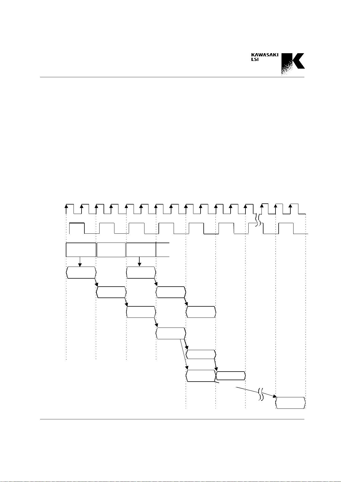
The example is shown in Fig. 4.5.1. The status of the internal
pipeline is also shown in the example. (Refer to Chapter 4.6
for more details.) The STR1/2_AUT command is executed
one wait after the external request for the search. The one
wait in this example is inserted because the idle time of one
PHASE signal is necessary to utilize the search result information such as a Hit. However, the STR_AUT command
should only be used when the cascade connection uses
external logic. (Refer to Chapter 5 for more details.)
For these STR commands, users can use the mask condition
defined by MS<3:0> pins or the CNTL1 register. When
using the CNTL1 register, this would be group C.
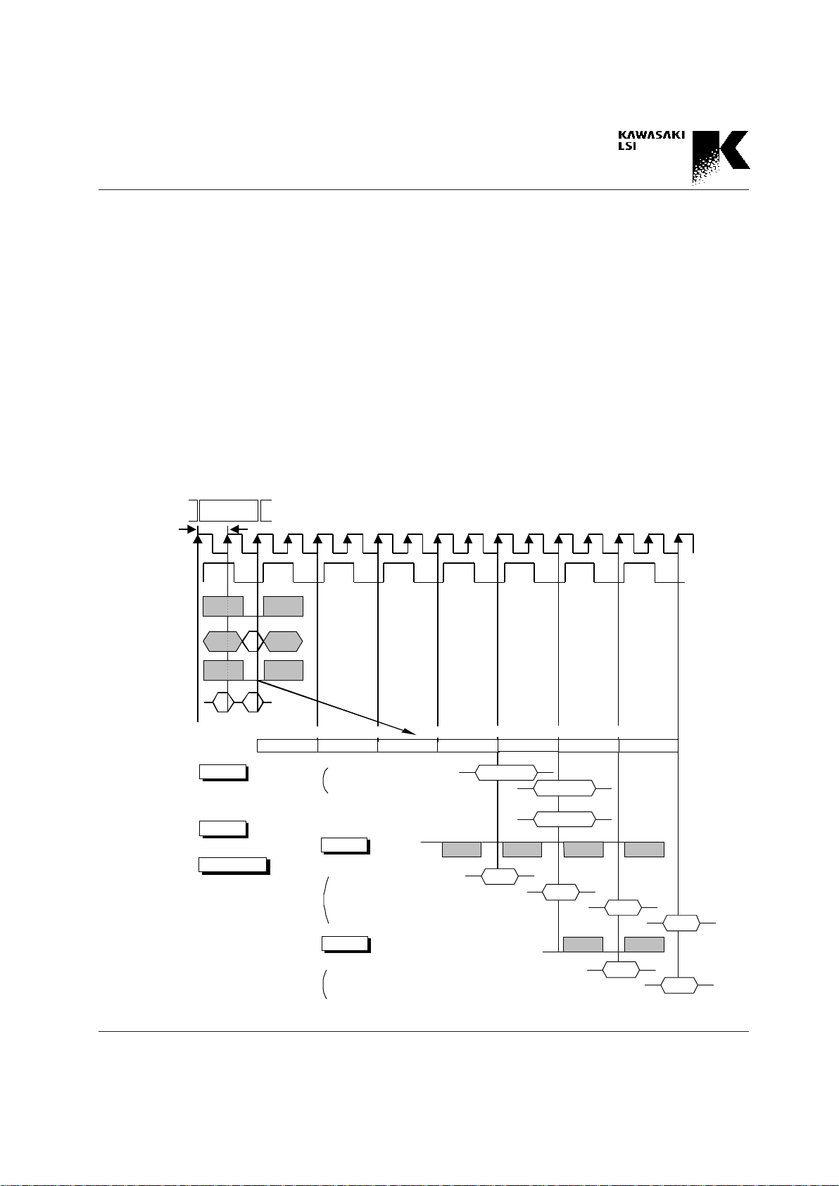
4.6 Restriction in Pipeline Operation
KE5BGCA128 is designed to use a maximum main clock of
66 MHz. This clock is synchronized with external requests,
resulting in operations which are processed by the internal
Pipeline. Internal Pipeline processing has several stages
corresponding to various requests for operation. When users request multiple operations continuously from the outside, these operations must be requested so that a conflict
between the Pipeline stages does not occur.
This Chapter describes the ways the internal pipeline
stages work to process the external request, and the rules
for continuous input of the various operations.
• Stages of pipeline
The following are five groups of stages of the Pipeline for
the operation request:
(1) Operation Request Stage
In this stage, the operation is requested through the CPU
bus, with the data and the address input being latched.
There are two kinds of stages, Read request stage and Write
request stage. The difference between these two stages depends upon whether the DAT bus is occupied. The Read
request stage does not occupy the DAT bus, but the Write
request stage occupies the DAT bus.
(2) Decode & Setup Stage
This stage follows the Operation Request Stage. The data or
the address that is latched in the Operation Request Stage is
decoded to recognize the request, and then the necessary
data is set up in this stage.
(3) Execute Stage
In this stage, the external request for operation is executed.
There are two kinds of operations, the operations that can
be executed with the other pipeline stage, See Fig. 4.5.1, and
the operations that cannot be executed with the other pipeline stage, according to which block in the device is executed.
(4) Wait/Nop Stage
This stage is for the timing adjustment of the internal bus
driving.
(5) Output Stage
Two stages, Output1 and Output2, are included. Output1 is
the stage for the output of the DAT bus, and Output2 is the
stage for the output of the OD bus. Output1 and Output2
can be executed simultaneously because these ports, DAT
bus and OD bus, are different ports.
• Processing and Pipeline Stages
The following seven Types are the categories of operation
according to the Pipeline Stages:
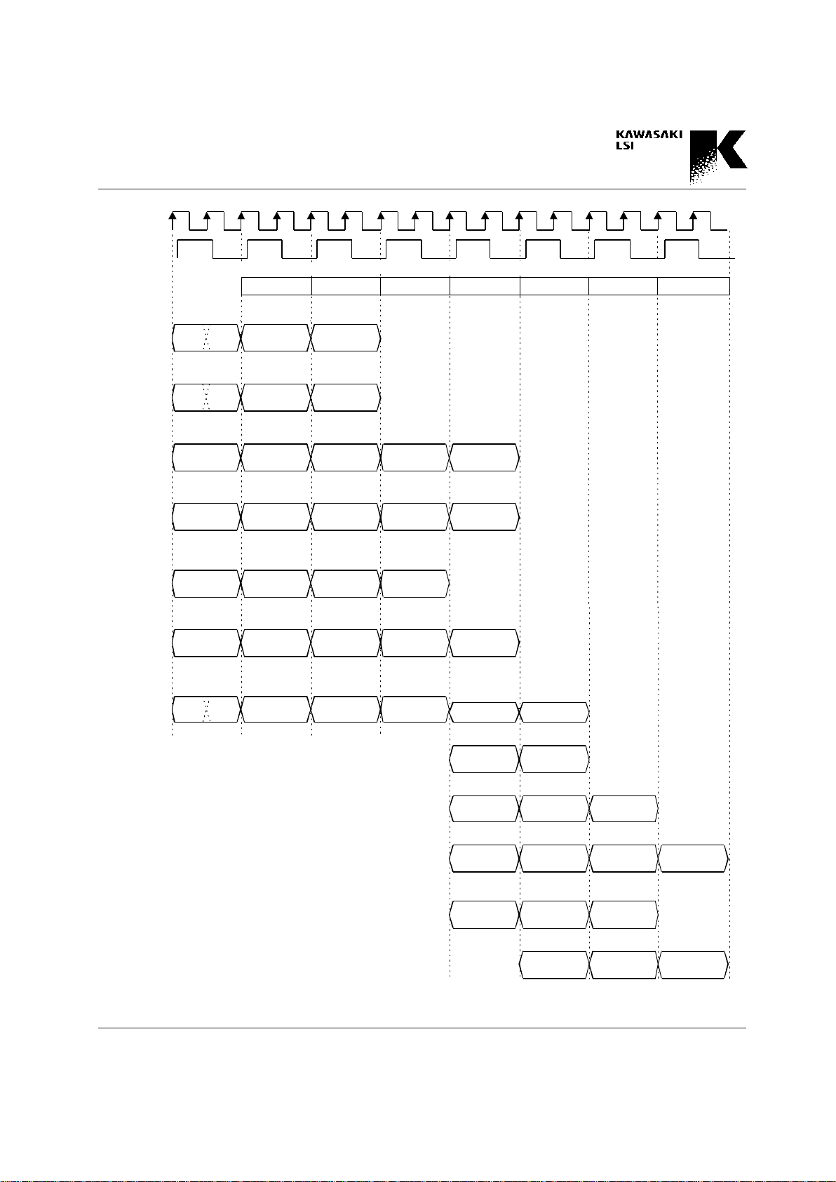
4-17
Preliminary
GigabitCAM KE5BGCA128
Fig. 4.6.1(a) Pipeline Operation Stage Chart
PHASE
Latency
CLK
Decode
& Setup
Execute0 Wait/Nop
Execute2
Decode
& Setup
Execute
Decode
& Setup
Execute Execute
Decode
& Setup
Execute Wait/Nop
Output1
(CPU)
Decode
& Setup
Execute
Output1
(CPU)
PinOut
Output2
(OD)
SHON
HHA
Execute1
Output2
(OD)
SHON/SMON
HHA
Output2
(OD)
HHA
Output2
(OD)
Wait/Nop
1) with HHA output
2) with MEMHHA output
Output2
(OD)
a)
b)
c)
Wait/Nop
Wait/Nop
Wait/Nop
Wait/Nop
Wait/Nop
PinOut
Execute1
Execute1
Execute2
HHA Latency : 5
Decode
& Setup
Execute
Decode
& Setup
Execute Wait/Nop
Output1
(CPU)
Execute0: SRCH operation
Execute1: HHA output operation from the OD bus
Execute2: MEMHHA output operation from the OD bus
Operation
Request(CPU)
Operation
Request(CPU)
Operation
Request(CPU)
Operation
Request(CPU)
Operation
Request(CPU)
Operation
Request(CPU)
Operation
Request(CPU)
HHA Latency : 6
HHA Latency : 7
a)
b)
MEMHHA Latency : 6
MEMHHA Latency : 7
MEMHHA
MEMHHA
Type 7 : SRCH operation with HHA output
Type 1 : Register write operation
Type 3 : Register (except HHA/HEA) read operation
Type 5 : 2-cycle command operation
Type 6 : HHA/HEA Register read operation
Type 2 : MEM write or 1-cycle command operation
Type 4 : MEM read operation
5 6 74
1
2
3
High Low
High Low
High Low
4-18
Preliminary
GigabitCAM KE5BGCA128
Type1: Registers write operation or 1 cycle command
operation
Type2: MEM* write operation *1
Type3: Registers (except HHA and HEA) read
operation
Type4: MEM* read operation *1
Type5: 2 -cycle command operation *2
Type6: HHA/HEA register read operation
Type7: SRCH operation with HHA read (with HEA
read)
*1): The read/write of the MEMHEAAI register is in
Type5.
*2): SRST, GEN_FL, NXT_HE, STR1_HEAAI,
STR1_AUTAI, STR2_HEAAI, STR2_AUTAI
commands
The Pipeline Stage timing of each Type is shown in Fig.
4.6.1. As shown in Fig. 4.6.1(a), the Operation Request Stage
in Type 1, 2, 7 is divided into two stages (High and Low)
because the 64-bit data could possibly be written to the
register or to the CAM word using the Fast Write Mode (64bit access per one PHASE signal cycle).
• Restriction of simultaneous execution of
Pipeline Stages
There are some restrictions of simultaneous executions of
the internal Pipeline Stages. Basically, the simultaneous ex-
ecution of the different Pipeline Stages is possible if they are in
different Pipelines, but the simultaneous execution must meet the
following restrictions:
1) The Write Request of the Operation Request Stage and
the Output1 Stage must not be executed
simultaneously because they use the same bus (DAT
bus).
2) Any operation can execute simultaneously during
Wait/Nop Stages.
3) The possible simultaneous operations of the Execute
Stages between the multiple Pipelines are restricted to
the following 3 cases:
a) The Execute of Type5 and the Execute of Types 1- 7
b) The Execute of Type6 and the Execute of Types 1- 7
c) The Execute1 and the Execute2 of Type7 and the
Execute of Types 1- 6
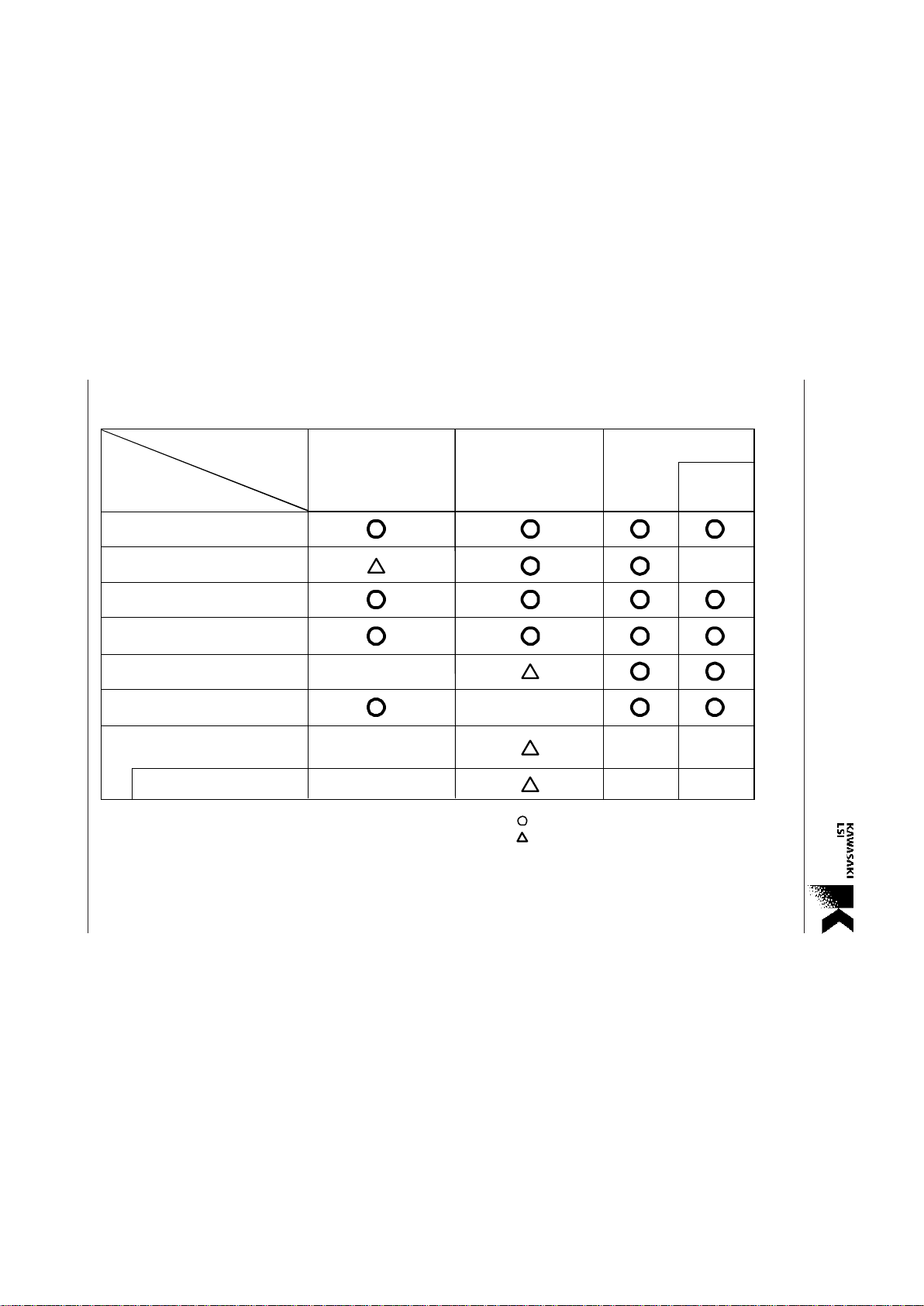
These executions must follow the restriction shown in Table
4.6.1. The column of the Table 4.6.1 means Execute stage which is
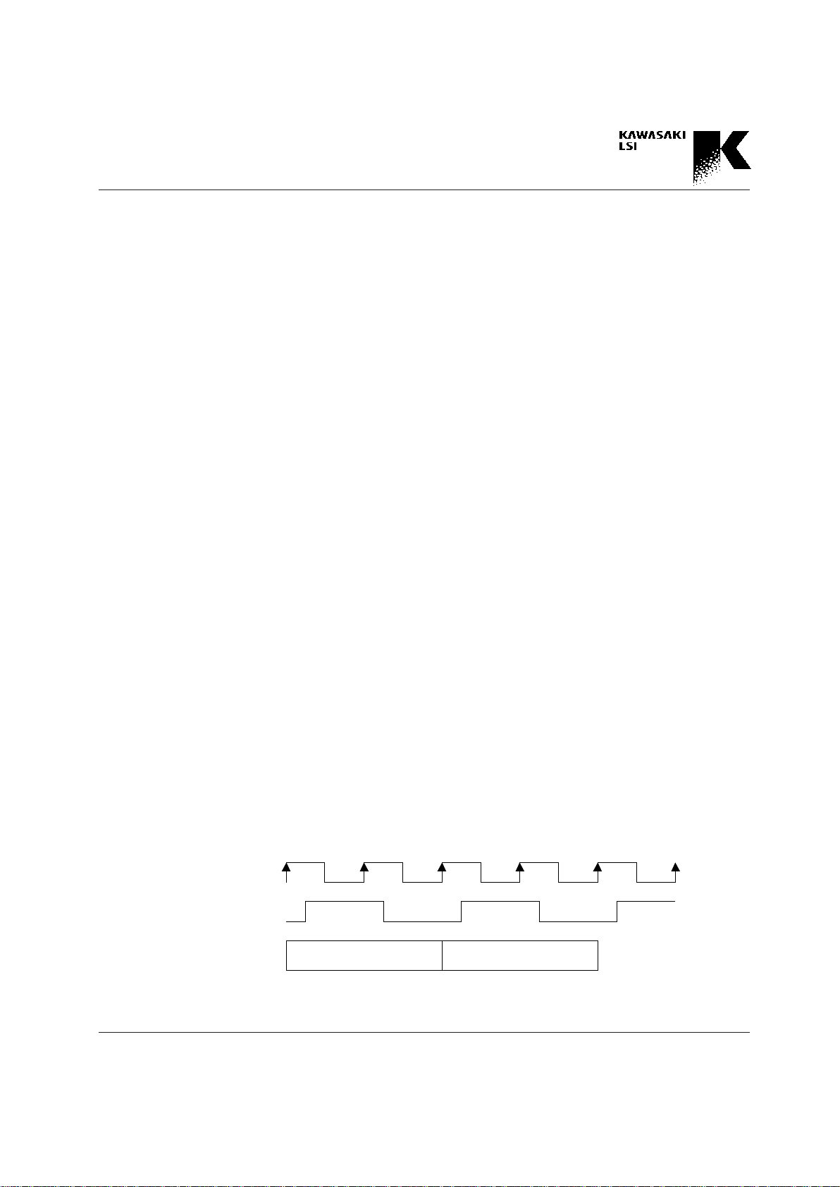
possible to simultaneously execute. As shown in Fig. 4.6.1 (b),
the the column of the table means 1st Input Operation, and the
row of the table means 2nd Input Operation.
CLK
PHASE
Input
Operation
1st Input Operation 2nd Input Operation
Fig. 4.6.1(b) Restriction of pipeline
4-19
Preliminary
GigabitCAM KE5BGCA128
with MEMHHA output
Type 1 :
Register write operation
Type 3 :
read operation
2-cycle command operation, MEMHEAAI
Type 6 :
HHA/HEA Register
read operation
Type 2 :
MEM_HHA, _HEA, _AR, _ARAI
write or 1-cycle command operation
Type 4 :
MEM_HHA, _HEA, _AR, _ARAI
with HHA output
with MEMHHA
output
Type 7 :
SRCH operation
Type 5 :
2-cycle command
operation *4)
Type 6 :
HHA/HEA Register
read operation
Type 7 :
SRCH operation with HHA output
*2)
*3) *3)
X
read operation
Register (except HHA/HEA)
Type 5:
1st Input
Operation
2nd Input
Operation
*1)
*5)
*6)
*6)
*1) Only the NXT_HE command and MEM write can be simultaneously executed.
*2) Impossible to simultaneously execute with the Execute 0 of the SRCH operation.
*3) Impossible to simultaneously execute with the write to the CNTL2 register.
*4) In case of the SRST command, reset operation has priority.
*5) Execute of the HEA read operation cannot be simultaneously executed Execute of
the GEN_FL, NXT_HE, STR1/2_HEAAI, STR1/2_AUTAI (mis-hit case), and MEMHEAAI access.
*6) Execute of the HHA read operation cannot be simultaneously executed Execute of search operation.
Table 4.6.1 Restriction of pipeline
: allowed
: allowed partially
: not allowed
X
X
X
X
X
X
X
X
X
 Loading...