

Kawasaki LSI KE5BCCA4MCBP-A, KE5BCCA4MCBP-E Datasheet

Kawasaki LSI
4.7M Classification CAM PRELIMINARY
Version 2.3.8 Confidential
Contents
1. Features.........................................................................................1
2. Block Diagram...............................................................................2
3. Pin Descriptions ...........................................................................4
3.1. Pin Assignment...........................................................................................4
3.2. Pin Descriptions..........................................................................................4
4. Functional Descriptions...............................................................7
4.1. Overview.....................................................................................................7
4.2. Segment Structure ......................................................................................7
4.3. Output Format.............................................................................................7
4.4. CAM Table Example....................................................................................8
4.5. CNTL Bus (CNTL[13:0])..............................................................................9
4.6. Timing Chart..............................................................................................10
5. Command Descriptions..............................................................13
6. Register.......................................................................................15
7. Product Information ...................................................................15
7.1. Ordering Information .................................................................................15
7.2. Package Outline........................................................................................15
8. Electrical Characteristics...........................................................16
8.1. Absolute Maximum Rating ........................................................................16
8.2. Operating Range.......................................................................................16
8.3. DC Characteristics ....................................................................................16

Kawasaki LSI
4.7M Classification CAM PRELIMINARY
Version 2.3.8 1 Confidential
1. Features
The KE5BCCA4M is a high-performance Content Addressable Memory (CAM). The following
features enable high-speed and high-density “switching," “address filtering,” and "packet
classification" applications required for internetworking switching and routing:
• Density: 4.7Mbits Ternary or Binary
• Configurable table Size: 72-bit x 64k, 144-bit x 32k, 288-bit x 16k (Ternary or Binary)
• Mixed table size configuration:
Selected by each bank (8banks). Each bank can be individually configured as a 72-bit x 8K,
144-bit x 4K, or 288-bit x 2K (Ternary or Binary) table.
• Input Clock rate:
High-speed input mode: Double Data Rate
- Single rate clock mode: 100/83/66/50 MHz clock (CLK) and phase (PHASE)
- Double rate clock mode: 200/166/133/100MHz clock (CLK) and the half rate phase (PHASE)
Normal input mode: Single Data Rate with 100/83/66/50 MHz clock (CLK) and no phase signal
• High-speed search and deterministic latency:
-100: Sustained 100MLPS, 10ns per 144-bit maximum, 5 Cycles latency
-83: Sustained 83MLPS, 12ns per 144-bit maximum, 5 Cycles latency
-66: Sustained 66MLPS, 15ns per 144-bit maximum, 4 Cycles latency
-50: Sustained 50MLPS, 20ns per 144-bit maximum, 3 Cycles latency
• Dual-port architecture
• 72-bit I/O Port Data Bus:
144-bit per 10/12/15/20ns write-in throughput is possible in the high-speed input mode. 72-bit
I/O port data bus is also configurable as a 40-bit wide bus.
• 23-bit Output Port: Search results are output
• Multi-hit support (Highest Hit Address output)
• 18 x 72-bit Global MASK Registers
• Weighted Search without data sorting:
-100: N/A
-83: 13.8Mpps (32-bit), 11.9Mpps (64-bit), 5.2Mpps (128-bit)
-66: 11.0Mpps (32-bit), 9.4Mpps (64-bit), 4.1Mpps (128-bit)
-50: 8.3Mpps (32-bit), 7.1Mpps (64-bit), 3.1Mpps (128-bit)
Note: When data sorting is done in advance, the look up rate is 100/83/66/50Mpps respectively.
• Effective Command Set for Table Management:
- Purge (Invalidate) all the hit entries in one Cycle
- Automatic Learning
• Cascading:
Up to 8pcs --- Glueless without degradation in performance --- 72-bit x 512k table
Cascadable up to 32pcs --- Maximum 72-bit x 2M table
• External SRAM direct connection (Address bypass to SRAM)
• Space-saving package: 324-pin BGA (27mm x 27mm)
• Power supply: ‘1.8V(core) and 1.8V(I/O)’, or ‘1.8V(core) and 2.5V/3.3V(I/O)’
Kawasaki LSI
4.7M Classification CAM PRELIMINARY
Version 2.3.8 2 Confidential
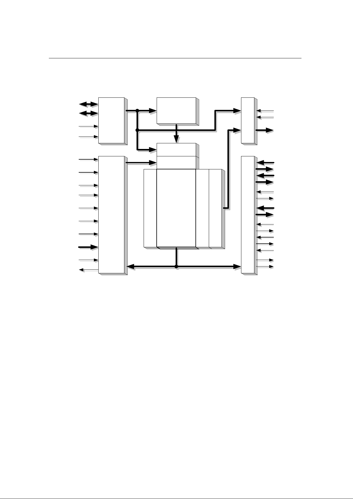
2. Block Diagram
Fig. 2-1 Functional Block Diagram
CEN
RWN
SAD
CLK
PHASE
RSTN
OEDATN
DAT[63:0]
EDAT[7:0]
DATWDT
CNTL[13:0]
PHOUN[1:0]
PHODN[1:0]
PMIN
PMON
FLIN[6:0]
FLON[1:0]
BHIDN
BHODN
BHIUN
BHOUN
BFLIN
SSHON
SMON
ODBYP
OEODN
OD[22:0]
PHIUN[6:0]
PHIDN[6:0]
INPMD
LMSTN
CLKMD
I/O
Port
Control
Control and
Status Registers
Pipeline
Execution
Control
Global Mask
Registers
CAM Control
Decoder
72bits x 65536
CAM
8 Banks
(72bitsx8Kx8)
structure
Mixable with
72bits x 8192
144bits x 4096
288bits x 2048
Empty Bit
Flag Control Output Port Control
Priority Encoder

Kawasaki LSI
4.7M Classification CAM PRELIMINARY
Version 2.3.8 3 Confidential
The KE5BCCA4M has the following components:
• I/O Port Control
I/O port to input search key data and read/write data. I/O port data bus can be configured as a
72-bit or 40-bit wide bus.
• Pipeline Execution Control
Controls operation with pipeline through the CNTL [13:0].
• Control/Status Register
Defines CAM functions.
• Mask Registers
18 Global Mask Registers in total: 16 72-bit wide user-definable registers and 2 fixed registers
(ALL 0 and ALL 1) for search and write operations.
• Search Logic/Control Logic
Controls CAM functions.
• CAM
72-bit x 64k CAM data table divided into 8 banks. Each bank can be individually defined as a
72-bit x 8k, 144-bit x 4k, or 288-bit x 2k (Binary/Ternary), and it is possible to search a specific
bank or several banks at the same time. By using these features, various kinds of data for
Layer-2, 3 and 4 can be stored in one device and managed in different ways.
• Output Port Control
Controls output port, which outputs search results. The DAT data bypass function is provided
for the external SRAM access through this CAM device.
• Flag Logic
Controls the flag status (e.g. Full and Hit). Interfaces with other devices in a cascaded system.
When the CAM table is divided into multiple blocks, the status of the searched block is output.
Kawasaki LSI
4.7M Classification CAM PRELIMINARY
Version 2.3.8 4 Confidential
3. Pin Descriptions
3.1. Pin Assignment
Refer to the datasheet.
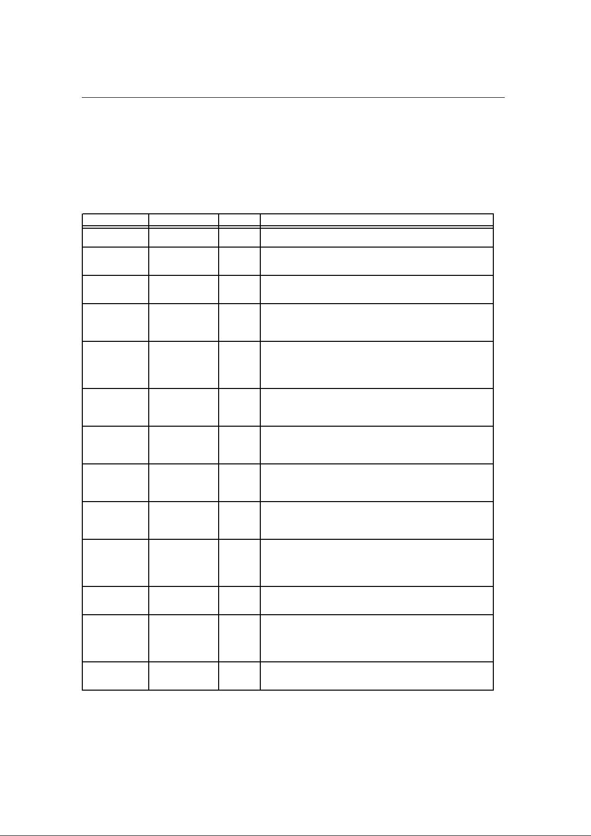
3.2. Pin Descriptions
Pin Name Description Attribute Function
RSTN Hardware Reset Input RSTN low resets the device.
CLK Clock Input CLK is the clock input. The rising edge of CLK is the timing
reference.
INPMD Input Mode Input INPMD determines the data input mode. Fix low in high-speed
input mode; fix high in normal speed input mode.
PHASE Phase Input PHASE determines the action timing of the device in high-speed
input mode. PHASE must be pulled down in normal input mode.
CLKMD Clock Mode Input CLKMD determines the CLK input method. Fix low in normal
speed input mode. In high-speed input mode, when supply
single rate clock, fix low and the double rate clock is generated
internally; when supply double rate clock, fix high.
DAT[63:0] I/O Port
Data Bus
Input/
Output
Tristate
DAT[63:0] is a 64-bit bi-directional data bus for read/write of
CAM memory and registers. RWN controls the bus direction.
EDAT[7:0] EXTRA Bit Data
Bus
Input/
Output
Tristate
EDAT[7:0] is a 8-bit bi-directional data bus for read/write of
EXTRA bits of CAM memory and registers. RWN controls the
bus direction.
DATWDT I/O Port Data Bus
Width
Input DATWDT defines DAT[63:0] width. Fix low to employ all
DAT[63:0]; fix high not to employ DAT[63:32] and to employ
DAT[31:0] with SAD as a substitute for DAT[63:0].
CNTL[13:0] Control Bus Input CNTL[13:0] is the 14-bit control bus to control the device. The
search operations, the command assertions, and the register
accesses are invoked corresponding to CNTL[13:0].
SAD Sub Address Input SAD assigns DAT[31:0] to internal 64-bit data bus when
DAT[63:32] is unused (DATWDT=high). When SAD is low,
DAT[31:0] is assigned to lower 32-bit; when high, it is assigned
to upper 32-bit.
CEN Device Enable Input CEN low invokes operations such as read/write, search and
command.
RWN Read/Write Input RWN determines the direction of the I/O Port data bus
DAT[63:0] and that of the EXTRA bit data bus EDAT[7:0]. RWN
low selects a write cycle and RWN high selects a read cycle.
OEDATN I/O Port Data Bus
Output Enable
Input OEDATN is output enable signal for DAT[63:0] and EDAT[7:0].
 Loading...