

Page 1

KS152JB Universal Communications Controller
Technical Specifications
1.0 INTRODUCTION
The 80C152 Universal Communications Controller is an 8-bit microcontroller designed for the
intelligent management of peripheral systems or components. The 80C152 is a derivative of the
80C51 and retains the same functionality. These enhancements include: a high speed multi-protocol serial communication interface, two channels for DMA transfers, HOLD/HLD A b us control, a
fifth I/O port, expanded data memory, and expanded program memory.
In addition to a standard UART, referred to here as Local Serial Channel (LSC), the 80C152 has
an on-board multi-protocol communication controller called the Global Serial Channel (GSC).
The GSC interface supports SDLC, CSMA/CD, user definable protocols, and a subset of HDLC
protocols. The GSC capabilities include: address recognition, collision resolution, CRC generation, flag generation, automatic retransmission, and a hardware based acknowledge feature. This
high speed serial channel is capable of implementing the Data Link Layer and the Physical Link
Layer as shown in the OSI open systems communication model. This model can be found in the
document “Reference Model for Open Systems Interconnection Architecture”, ISO/TC97/SC16
N309.
The DMA circuitry consists of two 8-bit DMA channels with 16-bit addressability. The control
signals; Read (RD), Write (WR), hold and hold acknowledge (HOLD/HLDA) are used to access
external memory. The DMA channels are capable of addressing up to 64K bytes (16 bits). The
destination or source address can be automatically incremented. The lower 8 bits of the address
can be automatically incremented. The lower 8 bits of the address are multiplexed on the data bus
Port 0 and the upper eight bits of address will be on Port 2. Data is transmitted over an 8-bit
address/data bus. Up to 64k bytes of data may be transmitted for each DMA activation.
The new I/O port (P4) function the same as Ports 1-3 found on the 80C51.
Internal memory has been doubled in the 80C152. Data memory has been expanded to 256 bytes,
and internal program memory has been expanded to 8 bytes.
There are also some specific differences between the 80C152 and the 80C51. The first difference
is that RESET is active low in the 80C152 and active high in the 80C51H. The second difference
is that GF0 and GF1, general purpose flags in PCON, have been renamed GFIEN and XRCLK.
GFIEN enables idle flags to be generated in SDLC mode, and XRCLK enables the receiver to be
externally clocked. All of the previously unused bits are now being used and interrupt vectors
have been added to support the new enhancements.
Throughout the rest of this manual the 80C152 will be referred to generically as the “C152”. The
C152 is based on the 80C51 architecture and utilizes the same 80C51 instruction set. There have
been no new instructions added. All the new features and peripherals are supported by an extension of the Special Function Registers (SFRs). A brief information on cpu functions as: the
instruction set, port operation, timer/counters, etc., is included in this document.
Kawasaki LSI USA, Inc. Page 1 of 120 Ver. 0.9 KS152JB2
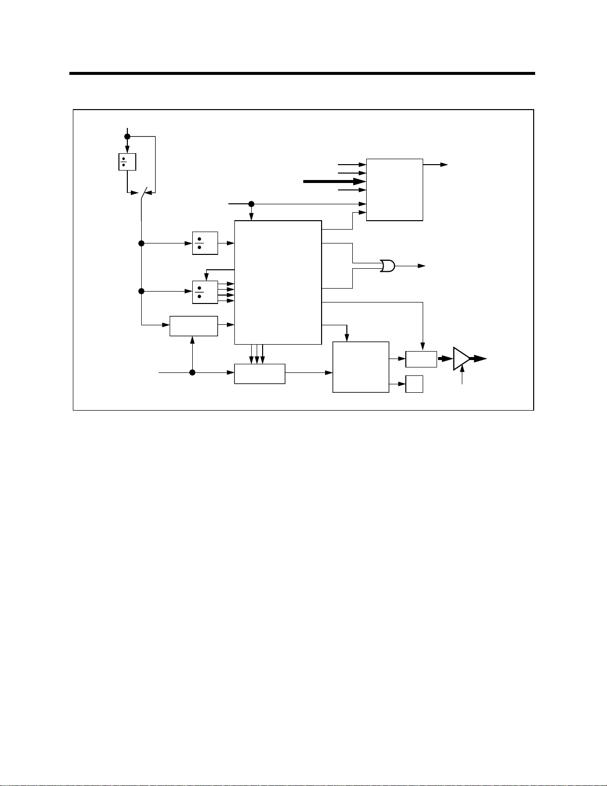
Page 2
KS152JB Universal Communications Controller
Technical Specifications
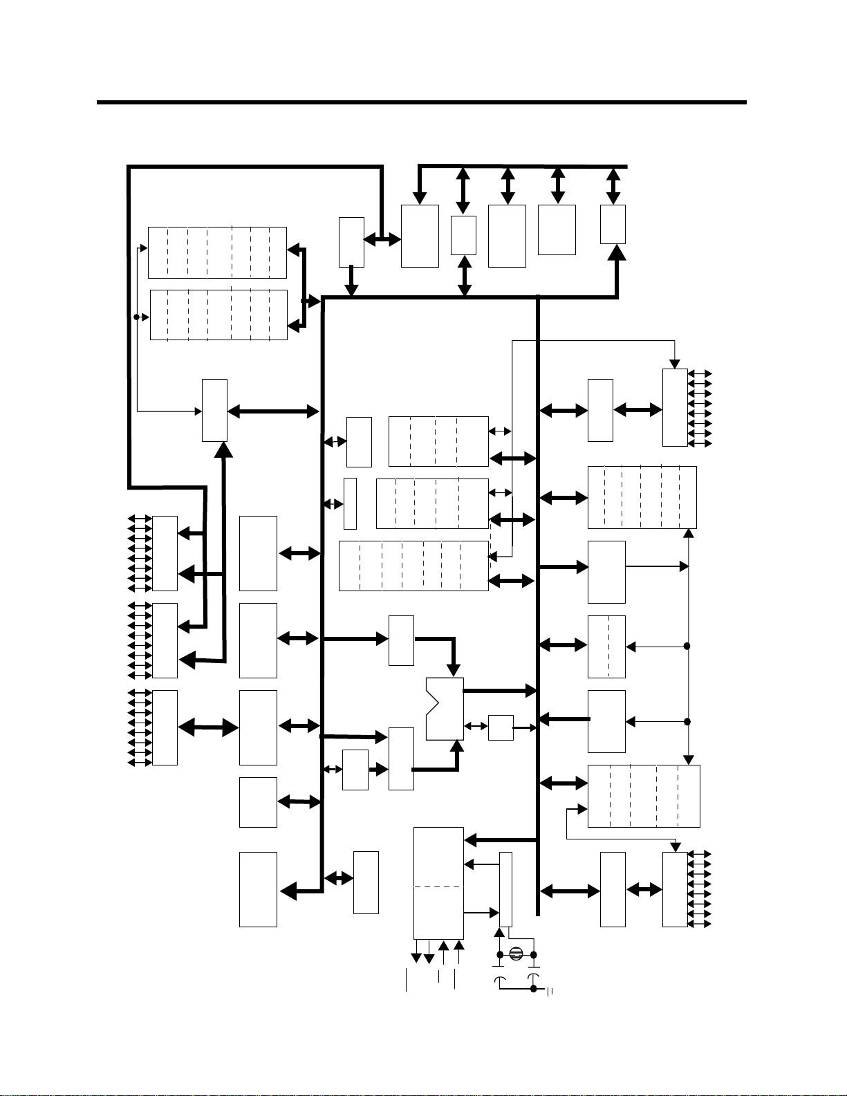
DCON0 DCON1
PORT 2
DIRVERS
SARL1
SARL0
SARH0
SARH1
DARL0
DMA
CONTROL
DARL1
DARH1
DARH0
PORT 2
BCRL1
BCRL0
LATCH
BCRH1
BCRH0
ROM
8K X 8
STACK
PCON
TCON
POINTER
IPN1
TMOD
TL0
PROGRAM
SBUF(RX)
IEN1
TH0
ADDRESS
SBUF(TX)
SCON
IP
IE
TL1
TH1
BUFFER
LOCAL
SERIAL
PORT
INTERRUPT
CONTROL
TIMER
CONTROL
PC
INCREMEN-
TER
PROGRAM
COUNTER
DPTR
PORT 3
LATCH
PRBS
SLOTTM
FIFO
TRANSMIT
PORT 3
DRIVERS
IFS
TSTAT
MYSLOT
P3.0 - P3.7
TCDCNT
PORT 0
PORT 0
DRIVERS
P4.0 - P4.7 P0.0 - P0.7 P2.0 - P2.7
PORT 4
DRIVERS
LATCH
PORT 4
LATCH
RAM
256 X 8
RAM
ADDRESS
REGISTER
ACC
B
REGISTER
TMP 1
TMP 2
PSEN
INSTRUCT-
ION
REGISTER
TIMING
AND
ALE
CONTROL
EA
ALU
RST
XTAL1
PSW
OSCILLATOR
XTAL2
RSTAT
AMSKO-1
RECEIVE
FIFO
GSC
CONTROL
PORT1
LATCH
CRC
GMOD
GENERATOR
ADRO-3
PORT1
DRIVERS
BAUD
P1.0 - P1.7
Kawasaki LSI USA, Inc. Page 2 of 120 Ver. 0.9 KS152JB2
Page 3

KS152JB Universal Communications Controller
Technical Specifications
2.1 Pin Description
Table 1: PIN DESCRIPTION
Name Description
Port 0 Port 0 is an 8-bit open drain bi-directional I/O Port. As an output port each pin can
sink 8 LS TTL inputs. Port 0 pins that have 1s written to them float, and in that
state can be used as high-impedance inputs.
external program memory if EBEN is pulled low. During accesses to external
Data Memory, Port 0 always emits the low-order address byte and serves as the
multiplexed data bus. In these applications it uses strong internal pullups when
emitting 1s.
Port 0 also outputs the code bytes during program verification. External pullups
are required during program verification.
Port 1 Port 1 is an 8 -bit bidirectional I/O port with internal pullups. Port 1 pins that have
1s written to them are pulled high by the internal pullups, and in that state can be
used as inputs. As inputs, Port 1 pins that are externally being pulled low will
source current (I
Port 1 also serves the functions of various special features of the 8XC152, as listed
below:
, on the data sheet) because of the internal pullups.
IL
Pin Name Alternate Function
P1.0 GRXD GSC data input pin
P1.1 GTXD GSC data output pin
P1.2 DEN
P1.3
P1.4
P1.5 HLD DMA hold input/output
P1.6 HLDA DMA hold acknowledge input/output
Port 2 Port 2 is an 8-bit bi-directional I/O port with internal pullups. Port 2 pins that have
1s written to them are pulled high by the internal pullups, and in that state can be
used as inputs. As inputs, Port 2 pins that are externally being pulled low will
source current (I
the high-order address byte during fetches from external program memory if
EBEN is pulled low. During accesses to external Data Memory that use 16-bit
addresses (MOVX @ DPTR and DMA operations), Port 2 emits the high-order
address byte. In these applications it uses strong internal pullups when emitting
1s. During accesses to external Data Memory that use 8-bit addresses (MOVX @
Ri), Port2 emits the contents of the P2 Special Function Register. Port 2 also
receives the high-order address bits during program verification.
GSC enable signal for an external driver
TXC GSC input pin for external transmit clock
RXC GSC input pin for external receive clock
, on the data sheet) because of the internal pullups. port 2 emits
IL
Kawasaki LSI USA, Inc. Page 3 of 120 Ver. 0.9 KS152JB2
Page 4

KS152JB Universal Communications Controller
Technical Specifications
Table 1: PIN DESCRIPTION
Port 3 Port 3 is an 8-bit bi-directional I/O port with internal pullups. Port 3 pins that have
1s written to them are pulled high by the internal pullups, and in that state can be
used as inputs. As inputs, Port 3 pins that are externally being pulled low will
source current (I
functions of various special features of the MCS-51 Family, as listed below:
Pin Name Alternate Function
P3.0 RXD Serial input line
P3.1 TXD Serial output line
P3.2
P3.3
P3.4 T0 Timer 0 external input
P3.5 T1 Timer 1 external input
P3.6
P3.7
INT0 External interrupt 0
INT1 External interrupt 1
WR External Data Memory Write strobe
RD External Data Memory Read strobe
on the data sheet) because of the pullups. Port 3 also serves the
IL,
Port 4 Port 4 is an 8-bit bi-directional I/O port with internal pullups. Port 4 pins that have
1s written to them are pulled high by the internal pullups, and in that state can be
used as inputs. As inputs, Port 4 pins that are externally being pulled low will
source current (I
Port 4 also receives the low-order address bytes during program verification.
Port 5 Port 5 is an 8-bit bi-directional I/O port with internal pullups. Port 5 pins that have
1s written to them are pulled high by the internal pullups, and in that state can be
used as inputs. As inputs, Port 5 pins that are externally being pulled low will
source current (I
Port 5 is also the multiplexed low-order address and data bus during accesses to
external program memory if EBEN is puled high. In this application it uses strong
pullups when emitting 1s.
Port 6 Port 6 is an 8-bit bi-directional I/O port with internal pullups. Port 6 pins that have
1s written to them are pulled high by the internal pullups, and in that state can be
used as inputs. As inputs, Port 6 pins that are externally pulled low will source
current (I
high-order address byte during fetches from external Program Memory if EBEN
is pulled high. In this application it uses strong pullups when emitting 1s.
XTAL1 Input to the inv erting oscillator amplifier and input to the internal clock generating
circuits.
, on the data sheet) because of the internal pullups. Port 6 emits the
LL
on the data sheet) because of the internal pullups. In addition,
IL,
, on the data sheet) because of the internal pullups.
IL
XTAL2 Output from the oscillator amplifier.
RST Reset input. A logic low on this pin for three machine cycles while the oscillator is
running resets the device. An internal pullup resistor permits a power on reset to
be generated using only an external capacitor to V
nizes the reset after three machine cycles, data may continue to be transmitted for
up to 4 machine cycles after Reset is first applied.
Kawasaki LSI USA, Inc. Page 4 of 120 Ver. 0.9 KS152JB2
. Although the GSC recog-
SS
Page 5
KS152JB Universal Communications Controller
Technical Specifications
Table 1: PIN DESCRIPTION
ALE Address Latch Enable output signal for latching the low byte of the address during
accesses to external memory.
In normal operation ALE is emitted at a constant rate of 1/6 the oscillator frequency, and may be used for external timing or clocking purposes. Note, however,
that one ALE pulse is skipped during each access to external Data Memory. While
in Reset, ALE remains at a constant high level.
PSEN Program Store Enable is the Read strobe to External Program Memory. When the
8XC152 is executing from external program memory,
the device is executing code from External Program Memory,
twice each machine cycle, except that two
each access to External Data Memory. While in Reset,
stant high level.
EA External Access enable. EA must be externally pulled low in order to enable the
8XC152 to fetch code from External Program Memory locations 0000H to
0FFFH.
EA must be connected to VCC for internal program execution.
PSEN activations are skipped during
PSEN is active (lo w). When
PSEN is activated
PSEN remains at a con-
EBEN E-Bus Enable input that designates whether program memory fetches take place
via Ports 0 and 2 or ports 5 and 6. Table 2.1 shows how the ports are used in conjunction with EBEN.
EPSEN E-bus program Store Enable is the Read strobe to external program memory when
EBEN is high. Table 2.1 shows when
on the status of EBEN and
EA.
EPSEN is used relative to PSEN depending
Kawasaki LSI USA, Inc. Page 5 of 120 Ver. 0.9 KS152JB2
Page 6

KS152JB Universal Communications Controller
Technical Specifications
2.2 Special function Registers
The following table lists the SFR’s present in 80152. Note that not all the addresses are occupied
by SFR’s. The unoccupied addresses are not implemented and should not be used by the customer. Read access from these unoccupied locations will return unpredictable data, while write
accesses will have no effect on the chip
Table 2: SFR map for the cpu
F8 IPN1 FF
F0 B BCRL1 BCRH1 RFIFO MYSLOT F7
E8 RSTAT EF
E0 ACC BCRL0 BCRH0 PBRS AMSK1 E7
D8 TSTAT DF
D0 PSW DARL1 DARH1 TCDCNT AMSK0 D7
C8 IEN1 CF
C0 P4 DARL0 DARH0 BKOFF ADR3 C7
B8 IP BF
B0 P3 SARL1 SARH1 SLOTTM ADR2 B7
A8 IE AF
A0 P2 P6 SARL0 SARH0 IFS ADR1 A7
98 SCON SBUF 9F
90 P1 P5 DCON0 DCON1 BAUD ADR0 97
88 TCON TMOD TL0 TL1 TH0 TH1 8F
80 P0 SP DPL DPH GMOD TFIFO PCON 87
Note: SFR’s in marked column are bit addressable.
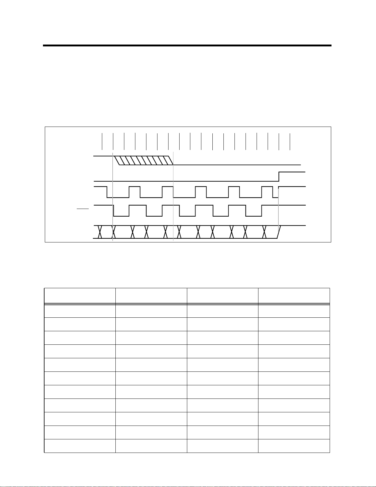
2.3 RESET
The RST pin is the input to a Schmitt Trigger whose output is used to generate the internal system
reset. In order to obtain a reset, the RST pin must be held low for at least four machine cycles,
while the oscillator is running. The CPU internal reset timings are shown in the Figure.
The external reset input RST is sampled on S5P2 in every machine cycle. If the sampled value is
high, then the processor responds with an internal reset signal at S3P1, two machine cycles after
the RST being sampled low. This means that there is an internal delay of 19 to 31 clock periods
Kawasaki LSI USA, Inc. Page 6 of 120 Ver. 0.9 KS152JB2
Page 7
KS152JB Universal Communications Controller
Technical Specifications
between the RST pin being pulled low and the internal reset being generated. During this time the
CPU continues its normal operations.
The internal reset signal clears the SFRs except the port SFRs which have FFh written into them
and the Stack Pointer which has 07h written to it. The SBUF is however in an indeterminate state.
The Program Counter is reset to 0000h. The internal RAM is not affected by the reset and their
contents remain unchanged. On power up, their contents is indeterminate.
RST
internal reset
ALE
PSEN
P0
S5 S6
S1 S2
ADDRINSTADDR
S3 S4
S5 S6
S1 S2
S3 S4
S5 S6
S1 S2
ADDRINSTADDRINSTADDRINSTADDRINST
S3 S4
Reset Timing
Table 3: Reset Values of the SFRs
SFR Name Reset Value SFR Name Reset Value
PC 0000H BRCL0-1 INDETERMINATE
ACC 00H BCRH0-1 INDETERMINATE
B 00H TL0 00H
PSW 00H TH0 00H
SP 07H TL1 00H
DPTR 0000H TH1 00H
P0-6 FFH ADR0-3 00H
RFIFO INDETERMINATE AMSK0-1 00H
RSTAT 00H BAUD 00H
SARH0-1 INDETERMINATE BKOFF INDETERMINATE
SARH0-1 INDETERMINATE SLOTTM 00H
Kawasaki LSI USA, Inc. Page 7 of 120 Ver. 0.9 KS152JB2
Page 8

KS152JB Universal Communications Controller
Technical Specifications
Table 3: Reset Values of the SFRs
SFR Name Reset Value SFR Name Reset Value
IP XXX00000B SCON 00H
IE 0XX00000B SBUF INDETERMINATE
TMOD 00H PCON 0XXX0000B
TCON 00H DARL0-1 INDETERMINATE
DCON0-1 00H DARh0-1 INDETERMINATE
GMOD X0000000B IFS 00H
IEN1 XX000000B MYSLOT 00H
IPN1 XX000000B PRBS 00H
TCDCNT INDETERMINATE TCON 00H
TFIFO INDETERMINATE TSTAT XX000100B
2.4 PORT STRUCTURES AND OPERATION
The ports are all bidirectional. Each port consists of two sections, the port SFR and the I/O pad.
The Ports 0 and 2 are involved in accesses to external memory. In this case, Port 0 outputs the
lower byte of the external memory address while port 2 outputs the higher byte of the external
address. The Port 0 bus is also used as a data bus for the data byte that is read or is to be written.
Therefore Port 0 is actually a time-multiplexed address/data bus. A point to note is that Port 2 outputs the upper 8 bits of the address only if the address is 16 bits wide, else it continues to emit the
Port 2 SFR contents.
In order that the alternate functions on the port pin are activated correctly, the corresponding bit
latch must be held at value 1. If this is not done then the corresponding port pin is stuck at 0, and
external or internal inputs will have no effect on the pin value.
I/O CONFIGURATIONS
Each individual port has different I/O pads to accommodate the different functions of each individual port. The figure below shows a simplified diagram of the I/O pads for each port.
Kawasaki LSI USA, Inc. Page 8 of 120 Ver. 0.9 KS152JB2
Page 9
KS152JB Universal Communications Controller
Technical Specifications
ADDR/DATA
IDNAMX
1
Q
MUX
PORT0OP
PORT0IP
0
1. Port 0 I/O Pad
PORT1OP
PORT1IP
2. Port 1 I/O Pad
VCC
VCC
Weak Internal
Pullup
P0.X
P1.X
ADDRESS
IDNAHI
Pin
PORT2OP
PORT2IP
1
MUX
0
VCC
Internal
Pullup
P2.X
Pin
Q
3. Port 2 I/O Pad
Alternate Output
Function
Pin
PORT3OP
Alternate Output
Function
PORT3IP
VCC
Weak Internal
Pullup
P3.X
Pin
4. Port 3,4,5 &6 I/O Pad
Port bit I/O Pads
As shown in Figure above, Ports 0 and 2 can emit either their respective SFR contents or the
ADDR/DATA and ADDRESS bus, depending upon the control lines IDNAMX and IDNAHI.
During external memory accesses, the P2 SFR remains unchanged, but the P0 SFR is preset to
FFh.
Ports 1, 2, 4, 5 and 6 have internal pullups, while Port 0 has an open drain output.
Every single I/O line can be individually configured as an input or output. However Ports 0 and 2
cannot be used as I/O ports since they are used as the ADDRESS/ DATA bus. To use any port pin
as an input, the corresponding bit latch must contain a 1. This turns off the active pulldown FET.
Then, for Ports 1, 2 and 3, the pin is pulled high by the internal pullup. The Internal pullup is a
weak pullup and so the pin can be pulled low by a strong external source.
Port 0, however has no internal pullups. The active pullup FET is used only when the port pin is
emitting a 1 during external memory accesses, else the pullup is off. Hence, when the port is used
as an I/O pin; IDNAMX is 1; the pullup FET is always off. Writing a 1 to the bit latch will turn off
the active pulldown FET and as a result the port pin will float.
As port 1, 2 and 3 have internal pullups, they will go high when configured as inputs and will
source current. Hence they are also known as “quasi-bidirectional” ports. Port 0 on the other hand
“floats” when configured as an input and hence is called a “true bidirectional” port.
Kawasaki LSI USA, Inc. Page 9 of 120 Ver. 0.9 KS152JB2
Page 10

KS152JB Universal Communications Controller
Technical Specifications
Writing to a Port
During the execution of an instruction that changes the value of a port SFR, the new value arrives
at the port latch during S6P2. However, the port latch contents do not appear on the port pins till
the next P1 phase. Therefore the new port data will appear on the port pins at S1P1 of the next
machine cycle.
Read-Modify-Write Feature
Each port is split into its SFR and its corresponding I/O pad. Therefore there are two options
available for a port read access. Either the SFR latch contents can be read or the input from the I/
O pads can be read. The instructions that read the latch, modify the value and write it back to the
latch are called “read-modify-write” instruction. In such instructions the latch and not the pin is
read. The instruction of this category are listed as follows
ANL logical AND
ORL logical OR
XRL logical XOR
JBC jump if bit = 1 and then clear bit
CPL complement bit
INC increment
DEC decrement
DJNZ decrement and jump if not zero
MOV PX.Y, C move carry bit to bit Y of Port X
CLR PX.Y clear bit Y of port X
SETB PX.Y set bit Y of X
2.5 Ports 4,5 and 6
Ports 4,5 and 6 operation is identical to Ports 1-3 on the 80C51. Ports 5 and 6 exist only on the
“JB” and “JD” version of the C152 and can either function as standard I/O ports or can be configured so that program memory fetches are performed with these two ports. To configure ports 5
and 6 as standard I/O ports, EBEN is tied to a logic low. When in this configuration, ports 5 and 6
operation is identical to that of port 4 except they are not bit addressable. To configure ports 5 and
6 to fetch program memory, EBEN is tied to a logic high. When using ports 5 and 6 to fetch the
program memory, the signal EPSEN is used to enable the external memory device instead of
PSEN. Regardless of which ports are used to fetch program memory, all data memory fetches
occur over ports 0 and 2. The 80C152JB and 80C152JD are available as ROMless devices only.
ALE is still used to latch the address in all configurations. Table 2.1 summarizes the control signals and how the ports may be used.
Kawasaki LSI USA, Inc. Page 10 of 120 Ver. 0.9 KS152JB2
Page 11

KS152JB Universal Communications Controller
Technical Specifications
Table 4:
EBEN
0 0 P0, P2 Active Inactive Addresses 0 - 0FFFFH
0 1 N/A N/A N/A Invalid Combination
1 0 P5, P6 Inactive Addresses 0 - 0FFFFH
1 1 P5, P6
EA Program
Fetch via
P0, P2
PSEN EPSEN Comments
Inactive
Active
Active
Inactive
Addresses 0 - 1FFFH
Addresses 0 - 2000H
2.6 ACCESSING EXTERNAL MEMORY
External Memory is accessed if either of the following two conditions is met
1) The signal
2) Whenever the program counter (PC) contains an address greater than 0FFFh.
Accesses to external memory are of two type: External Program Memory accesses and External
Data Memory accesses. External Program Memory is accessed using the
strobe. External Data Memory is accessed using the
EA is low
PSEN signal as the read
RD or WR pins to strobe the memory.
Fetches from the external Program Memory always use a 16 bit address, while External Data
Memory accesses can have addresses of 8 bit or 16 bit. Whenever a 16 bit address is used, Port 2
is used to emit the higher byte of the address. The point to note is that during external accesses,
port 2 uses strong pullups while emitting 1s. During the time Port 2 does not emit the higher
address byte, it continuously outputs the Port 2 SFR contents, which are not modified by the hardware (unless of course the user writes to the Port 2 SFR). If an 8 bit address is being used, then the
Port 2 SFR contents will be outputed on the port pins throughout the external memory cycle.
The lower byte of the address is always multiplexed with the data byte on Port 0. The ADDR/
DATA bus can drive both the active pullup and pulldown FETs. Thus for external memory
accesses, the port 0 pins are not open-drain outputs and do not need any external pullups. The falling edge of the ALE signal can be used to store the address on Ports 0 and 2 in an external address
latch. During a write cycle, the data to be written to the external Data Memory is present on Port 0
pins and remains there until after
pins is read just before the deactivation of the
During accesses to external memory, the CPU presets the Port 0 SFR to FFh in order to float the
Port 0 pins. Therefore any data that was present in the SFR latch will be lost. If the user, writes
any data other than FFh to Port 0 during an external memory cycle, then the incoming code byte
will be corrupted. Therefore, DO NOT WRITE TO Port 0 if external memory is used.
WR is deactivated. In case of a read access, the data on Port 0
RD signal.
Kawasaki LSI USA, Inc. Page 11 of 120 Ver. 0.9 KS152JB2
Page 12

KS152JB Universal Communications Controller
Technical Specifications
During External Memory Accesses, both Ports 0 and 2 are used for Address/ Data transfer and
therefore cannot be used for general I/O purposes. During external program fetches, Port 2 uses
strong pullups to emit 1s.
2.7 TIMER/COUNTERS
This has two 16-bit Timer/Counters, TM0 andTM1. Each of these Timer/Counters has two 8 bit
registers which form the 16 bit counting register. For T imer/Counter TM0 the y are TH0, the upper
8 bits register and TL0, the lower 8 bit register. Similarly Timer/Counter TM1 has two 8 bit registers, TH1 and TL1 and Timer/Counter
When configured as a “Timer”, the register is incremented once every machine cycle. Since a
machine cycle consists of 12 clock periods, the timer clock can be thought of as 1/12 of the master
clock. In the “Counter” mode, the register is incremented on the falling edge of the external input
pin, T0 in case of TM0, T1 for TM1. The T0, T1 inputs are sampled in every machine cycle at
S5P2. If the sampled value is high in one machine cycle and low in the next, then a valid high to
low transition on the pin is recognized and the count register is incremented. Since it takes two
machine cycles to recognize a negative transition on the pin, the maximum rate at which counting
will take place is 1/24 of the master clock frequency. In either the “Timer” or “Counter” mode, the
count register will be updated in S3P1. Therefore, in the “Timer” mode, the recognized negative
transition on pin T0 and T1 can cause the count register value to be updated only in the machine
cycle following the one in which the negative edge was detected.
76543210
GATE C/T M1 M0 GATE C/T M1 M0
Timer 1 Timer 0
GATE This bit controls the gating operations. When this bit is set, the Timer/Counter “x”
C/T This bit selects the Timer or Counter mode of operation. If this bit is set then the
is enabled only while “INTx” pin is high and “TRx” bit is set high. If this bit is
cleared, then Timer/Counter “x” is enabled only if “TRx” is set.
Counter mode is selected, else the Timer mode is selected.
M1 and M0 selects the operating mode for the Timer/CounterM1, M0
M1 M0
0 0 “THx” acts as a 8 bit Timer/Counter, with “TLx” as the 5 bit prescaler.
0 1 “THx” and “TLx” are cascaded to form a single 16 bit Timer/Counter.
1 0 This is the Auto Reload mode.
11
Timer 0: TL0 is an 8 bit Timer/Counter controlled by the Timer 0
control bits. TH0 is a 8 bit timer controlled by the Timer 1 control bits.
Timer 1: Timer/Counter is stopped.
Operating Mode
TMOD: Timer/Counter Mode Control Register
Kawasaki LSI USA, Inc. Page 12 of 120 Ver. 0.9 KS152JB2
Page 13

KS152JB Universal Communications Controller
Technical Specifications
76543210
TF1 TR1 TF0 TR0 IE1 IT1 IE0 IT0
TF1 Timer 1 overflow flag. Set by hardware on Timer/Counter overflow. Cleared by
TF0
TR0
IE1
IT1
IE0
IT0
hardware when processor vectors to timer 1 interrupt routine.
Timer 1 Run control bit. Set/Cleared by software to turn Timer/Counter on/off.TR1
Timer 0 overflow flag. Set by hardware on Timer/Counter overflow. Cleared by
hardware when processor vectors to timer 0 interrupt routine.
Timer 0 Run control bit. Set/Cleared by software to turn Timer/Counter on/off.
Interrupt 1 Edge flag. Set by hardware when external interrupt edge is detected.
Cleared when interrupt is processed.
Interrupt 1 Type control bit. Set/ Cleared by software to specify falling edge/low
level triggered external interrupt.
Interrupt 0 Edge flag. Set by hardware when external interrupt edge id detected.
Cleared when interrupt is processed.
Interrupt 0 Type control bit. Set/Cleared by software to specify falling edge /low
level triggered external interrupt.
TCON: Timer/Counter Control Register.
The “Timer” or “Counter” function is selected by the “C/T” bit in the TMOD Special Function
Register. Each Timer/Counter has one selection bit for its own; bit 2 of TMOD selects the function for Timer/Counter 0 and bit 6 of TMOD selects the function for Timer/Counter 1. In addition
each Timer/Counter can be set to operate in any one of four possible modes. The mode selection
is done by bits M0 and M1 in the TMOD SFR. Modes 0, 1 and 2 are identical for both the Timer/
Counters, but Mode 3 is different. The four modes of operation are described below.
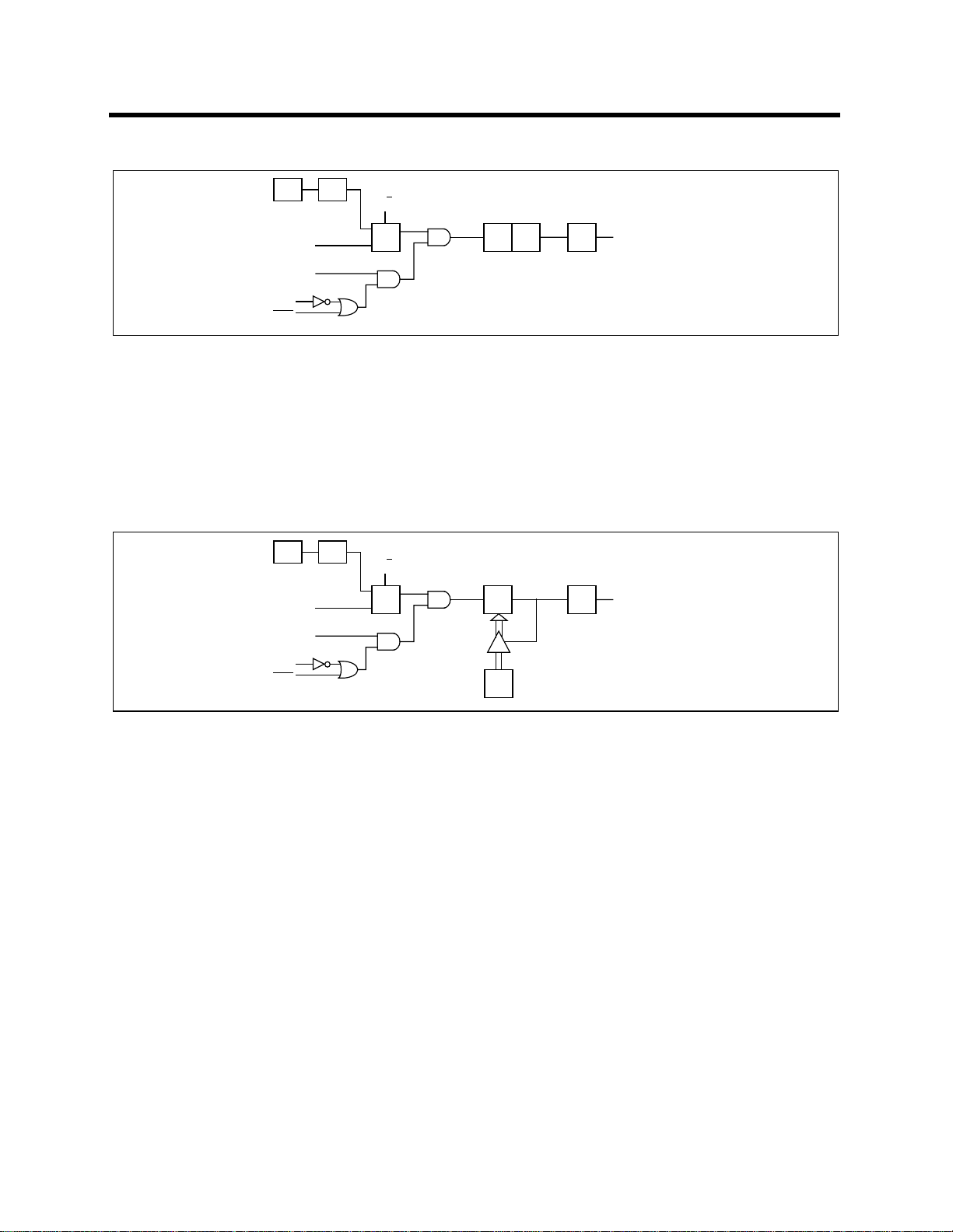
MODE 0
In Mode 0, the timer/counters act as a 8 bit counter with a 5 bit, divide by 32 prescaler. In this
mode we have a 13 bit timer/counter. The 13 bit counter consists of 8 bits of THx and 5 lower bits
of TLx. The upper 3 bits of TLx are ignored.
The negative edge of the clock increments the count in the TLx register. When the fifth bit in TLx
moves from 1 to 0, then the count in the THx register is incremented. When the count in THx
moves from FFh to 00h, then the overflow flag TFx in TCON SFR is set.
The counted input is enabled only if TRx is set and either GATE = 0 or
Kawasaki LSI USA, Inc. Page 13 of 120 Ver. 0.9 KS152JB2
INTx = 1.
Page 14
KS152JB Universal Communications Controller
Technical Specifications
GATE
INTx
S3P1OSC
Tx pin
TRx
pin
C/T
I0
Q
I1
TLX
5 bits
THx
8 bits
TFx
INTERRUPT
Timer/Counter in Mode 0
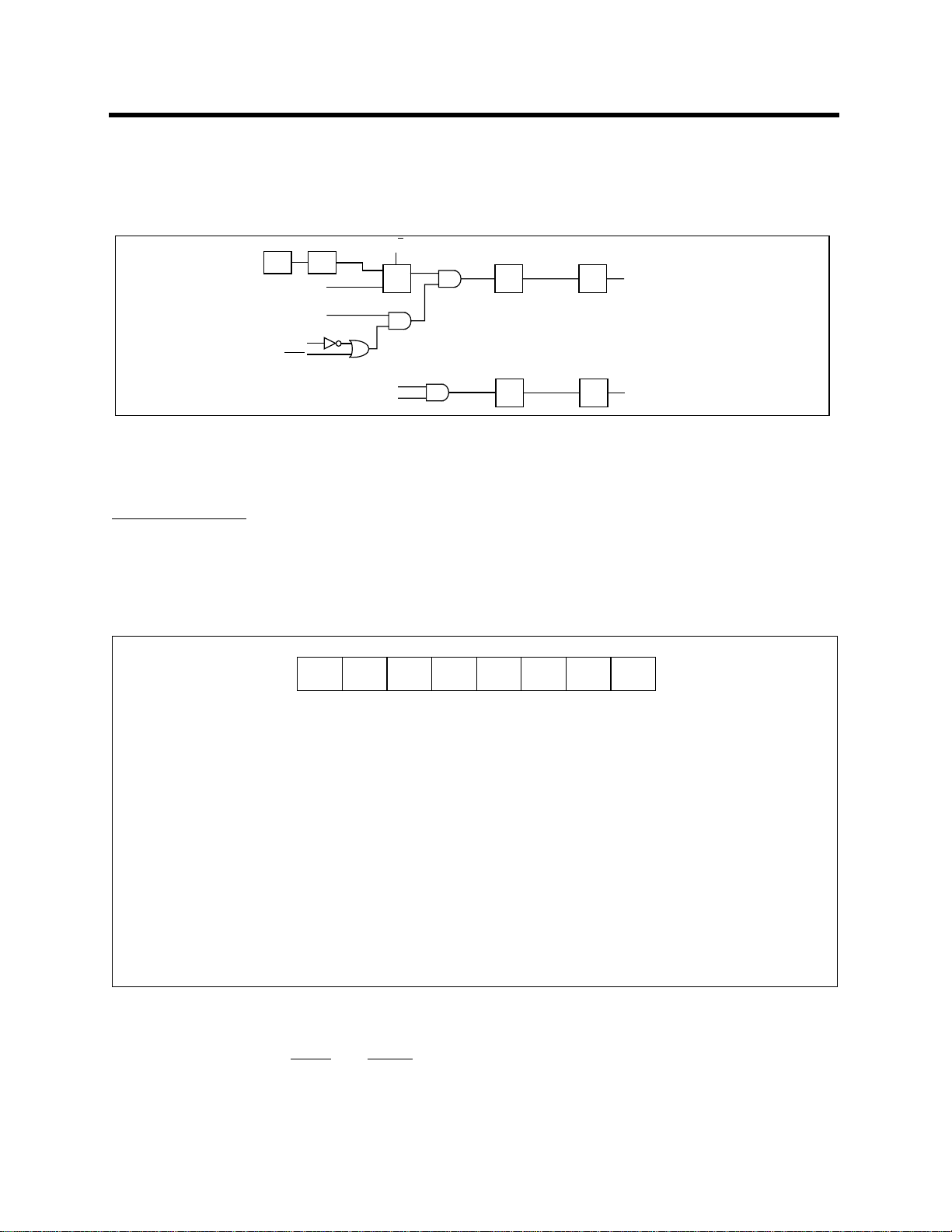
MODE 1
Mode 1 is similar to Mode 0 except that the counting register form a 16 bit counter, rather than a
13 bit counter. This means that all the bits of THx and TLx are used.
.
GATE
INTx
S3P1OSC
Tx pin
TRx
pin
C/T
I0
Q
I1
TLX
8 bits
THx
8 bits
Reload
TFx
INTERRUPT
Timer/Counter in Mode 2
MODE 2
In Mode 2, the timer/counter is in the Auto Reload Mode. In this mode, TLx acts as a 8 bit count
register, while THx holds the reload value. When the TLx register overflows from FFh to 00h, the
TFx bit in TCON is set and TLx is reloaded with the contents of THx and the counting process
continues from here. The reload operation leaves the contents of the THx register unchanged
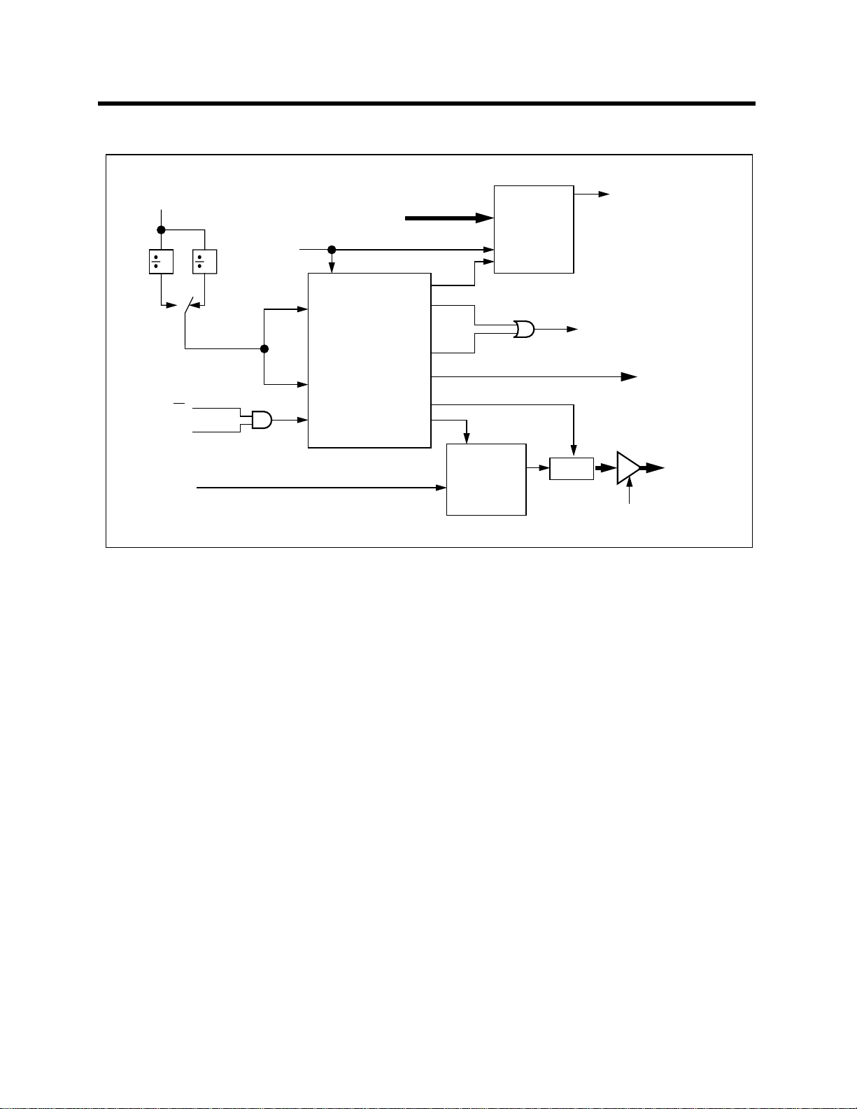
MODE 3
Mode 3 has different operating methods for the two timer/counters. For timer/counter TM1, mode
3 simply freezes the counter. This is the same as setting TR1 to 0.
Timer/Counter TM0 ho wever configures TL0 and TH0 as two separate 8 bit count registers in this
mode. The logic for this mode is shown in the figure. TL0 uses the Timer/Counter TM0 control
bits C/T, GATE, TR0, INT0 and TF0. TH0 is forced as a machine cycle counter and takes over the
use of TR1 and TF1 from Timer/Counter TM1.
Kawasaki LSI USA, Inc. Page 14 of 120 Ver. 0.9 KS152JB2
Page 15
KS152JB Universal Communications Controller
Technical Specifications
Mode 3 is used in cases where an extra 8 bit timer is needed. W ith T imer 0 in Mode 3, Timer 1 can
be turned on and off by switching it out of and into its own Mode 3. It can also be used as a baud
rate generator for the serial port.
C/T
GATE
INT0
pin
S3P1OSC
T0 pin
TR0
S3P1
TR1
I0
Q
I1
TL0
5 bits
TH0
8 bits
Timer/Counter 0 in Mode 3
TF0
TF1
INTERRUPT
INTERRUPT
2.8 Interrupts
The cpu has a provision for 11 different interrupt sources. These are the two external interrupts,
the three timer interrupts, the local serial port interrupt, dma interrupt and global serial port interrupts.
76543210
EA -- -- ES ET1 EX1 ET0 EX0
EA Global Disable bit. If this bit is cleared it disables all the interrupts at once.
ES
ET1
EX1
ET0
EX0
If EA is 1 then interrupts can be individually enabled/disabled by setting or
clearing its own enable bit.
reserved.--
Local Serial port interrupt enable.
Timer 1 interrupt enable.
External interrupt 1 enable.
Timer 0 interrupt enable.
External interrupt 0 enable
IE: Interrupt Enable Register.
The External Interrupts
INT0 and INT1 can be either edge triggered or level triggered, depending
on bits IT0 and IT1. The bits IE0 and IE1 in the TCON register are the flags which are checked to
generate the interrupt. When an interrupt is generated by these external interrupt inputs, they will
be cleared on entering the Interrupt Service routine, only if the interrupt type is edge triggered. In
Kawasaki LSI USA, Inc. Page 15 of 120 Ver. 0.9 KS152JB2
Page 16

KS152JB Universal Communications Controller
Technical Specifications
case of level triggered interrupt, the IE0 and IE1 flags are not cleared and will have to be cleared
by the software. This is because in the level activated mode, it is the external requesting source
that controls the interrupt flag bit rather than the on-chip hardware.
The Timer 0 and 1 Interrupts are generated by the TF0 and TF1 flags. These flags are set by the
overflow in the Timer 0 and Timer 1. The TF0 and TF1 flags are automatically cleared by the
hardware when the timer interrupt is serviced.
The Timer 0 and 1 flags are set in S5P2 of the machine cycle in which the overflow occurs. The
values are polled in the next cycle.
The Local Serial block can generated interrupts on reception or transmission. There is however
only one interrupt source from the Local Serial block, which is obtained by oring the RI and TI
bits in the SCON SFR. These bits are not automatically cleared by the hardware and the user will
have to clear these bits using software.
All the bits that generate interrupts can be set or reset by hardware and thereby software initiated
interrupts can be generated. Each of the individual interrupts can be enabled or disabled by setting
or clearing a bit in the IE SFR. IE also has a global enable/disable bit EA, which can be cleared to
disable all the interrupts at once.
Priority Level Structure
There are two priority levels for the interrupts. Each interrupt source can be individually set to
either one of the two levels. Naturally, a higher priority interrupt cannot be interrupted by a lower
priority interrupt. However there exists a predefined hierarchy amongst the interrupts themselves.
This hierarchy comes into play when the interrupt controller has to resolve simultaneous requests
having the same priority level. This hierarchy is defined as shown below, the interrupts are numbered starting from the highest priority to the lowest.
76543210
-- -- -- PS PT1 PX1 PT0 PX0
reserved.-PS
PT1
PX1
PT0
PX0
Local Serial port interrupt priority bit.
Timer 1 interrupt priority bit.
External interrupt 1 priority bit.
Timer 0 interrupt priority bit.
External interrupt 0 priority bit
IE: Interrupt Enable Register.
Kawasaki LSI USA, Inc. Page 16 of 120 Ver. 0.9 KS152JB2
Page 17

KS152JB Universal Communications Controller
Technical Specifications
01234567
EDMA1 EGSTV EDMA0 EGSRE EGSRVEGSTE
IEN1 (Additional interrupt enable register) (0C8H)
Interrupt enable register for DMA and GSC interrupts. A 1 in any bit position enables that interrupt.
IEN1.0 (EGSRV) - Enables the GSC valid receive interrupt.
IEN1.1 (EGSRE) - Enables the GSC receive error interrupt.
IEN1.2 (EDMA0) - Enables the DMA done interrupt for channel 0.
IEN1.3 (EGSTV) - Enables the GSC valid transmit interrupt.
IEN1.4 (EDMA1) - Enables the DMA done interrupt for Channel1.
IEN1.5 (EGSTE) - Enables the GSC transmit error interrupt.
01234567
PDMA1 PGSTV PDMA0 PGSRE PGSRVPGSTE
IPN1 (Additional interrupt priority register) (0F8H)
Allows the user software two levels of prioritization to be assigned to each of the interrupts in
IEN1. A 1 assigns the corresponding interrupt in IEN1 a higher interrupt than an interrupt with a
corresponding 0.
IPN1.0 (PGSRV) - Assigns the priority of GSC receive valid interrupt.
IPN1.1 (PGSRE) - Assigns the priority of GSC error receive interrupt.
IPN1.2 (PDMA0) - Assigns the priority of DMA done interrupt for Channel 0.
IPN1.3 (PGSTV) - Assigns the priority of GSC transmit valid interrupt.
IPN1.4 (PDMA1) - Assigns the priority of DMA done interrupt for Channel 1.
IPN1.5 (PGSTE) - Assigns the priority of GSC transmit error interrupt.
Kawasaki LSI USA, Inc. Page 17 of 120 Ver. 0.9 KS152JB2
Page 18

KS152JB Universal Communications Controller
Technical Specifications
The interrupt flags are sampled in S5P2 of every machine cycle. In the next machine cycle, the
sampled interrupts are polled and their priority is resolved. If certain conditions are met then the
hardware will execute an internally generated LCALL instruction which will v ector the process to
the appropriate interrupt vector address. The conditions for generating the LCALL are
1. An interrupt of equal or higher priority is not currently being serviced.
2. The current polling cycle is the last machine cycle of the instruction currently being executed.
3. The current instruction does not involve a write to IP or IE registers and is not a RETI.
If any of these conditions are not met, then the LCALL will not be generated. The polling cycle is
repeated every machine cycle, with the interrupts sampled at S5P2 in the previous machine cycle.
If an interrupt flag is active in one cycle but not responded to, and is not active when the above
conditions are met, the denied interrupt will not be serviced. This means that active interrupts are
not remembered, every polling cycle is new.
The processor responds to a valid interrupts by ex ecuting an LCALL instruction to the appropriate
service routine. This may or may not clear the flag which caused the interrupt. In case of Timer
interrupts, the TF0 or TF1 flags, are cleared by hardware whenever the processor vectors to the
appropriate timer service routine. In case of External interrupt, I
cleared only if they are edge triggered. In case of Local Serial interrupts, the flags are not cleared
by hardware. The hardware LCALL behaves exactly like the software LCALL instruction. This
instruction saves the Program Counter contents onto the Stack, b ut does not sa v e the Program Status Word PSW. The PC is reloaded with the vector address of that interrupt which caused the
LCALL. These vector address for the different sources are as follows
Table 5:
Priority
sequence
1 IP.0 PX0 IE.0 EX0 03H
2 IPN1.0 PGSRV IEN1.0 EGSRV 2BH
3 IP.1 PT0 IE.1 ET0 0BH
Priority
address
Priority
name
Interrupt
Symbolic
name
NT0 and INT1, the flags are
Interrupt
Symbolic
Name
Vector
Address
4 IPN1.1 PGSRE IEN1.1 EGSRE 33H
5 IPN1.2 PDMA0 IEN1.2 EDMA0 3BH
6 IP.2 PX1 IE.2 EX1 13H
7 IPN1.3 PGSTV IEN1.3 EGSTV 43H
Kawasaki LSI USA, Inc. Page 18 of 120 Ver. 0.9 KS152JB2
Page 19

KS152JB Universal Communications Controller
Technical Specifications
Table 5:
Priority
sequence
8 IPN1.4 PDMA1 IEN1.4 EDMA1 53H
9 IP.3 PT1 1E.3 ET1 1BH
10 IPN1.5 PGSTE IEN1.5 EGSTE 4BH
11 IP.4 PS IE.4 ES 23H
Execution continues from the vectored address till an RETI instruction is executed. On execution
of the RETI instruction the processor pops the Stack and loads the PC with the contents at the top
of the stack. The user must take care that the status of the stack is restored to what is was after the
hardware LCALL, if the execution is to return to the interrupted program. The processor does not
notice anything if the stack contents are modified and will proceed with execution from the
address put back into PC. Note that a RET instruction would do exactly the same process as a
RETI instruction, but it would not inform the Interrupt Controller, that the interrupt service routine is completed, an would leave the controller still thinking that the service routine is under
progress.
Priority
address
Priority
name
Interrupt
Symbolic
name
Interrupt
Symbolic
Name
Vector
Address
External Interrupts
There are two external interrupt sources in this processor , INT0 and INT1. These interrupts can be
programmed to be edge triggered or level activated, by setting bits IT0 and IT1 in TCON SFR. In
the edge triggered mode, the INTx inputs are sampled at S5P2 in every machine c ycle. If the sample is high in one cycle and low in the next, then a high to low transition is detected and the interrupts request flag IEx in TCON is set. The flag bit the requests the interrupt.Since the external
interrupts are sampled every machine cycle, they have to be held high or low for at least on complete machine cycle. The IEx flag is automatically cleared when the service routine is called.
If the level activated mode is selected, then the requesting source has to hold the pin low till the
interrupt is serviced. The IEx flag will not be cleared by the hardware on entering the service routine. If the interrupt continues to be held low even after the service routine is completed, then the
processor may acknowledge another interrupt request from the same source.
Response Time
The response time for each interrupt source depends on several factors like nature of the interrupt
and the instruction under progress. In the case of external interrupt INT0 and INT1, they are sampled at S5P2 of every machine cycle and then their corresponding interrupt flags IE0 and IE1 will
be set or reset. Similarly, the Local Serial port flags RI and TI are set in S5P2. The Timer 0 and 1
overflow flags are set during S3 of the machine cycle in which overflow has occurred. These flag
Kawasaki LSI USA, Inc. Page 19 of 120 Ver. 0.9 KS152JB2
Page 20

KS152JB Universal Communications Controller
Technical Specifications
values are polled only in the next machine cycle. If a request is active and all three conditions are
met, then the hardware generated LCALL is executed. This call itself takes tw o machine cycles to
be completed. Thus there is a minimum time of three machine cycles between the interrupt flag
being set and the interrupt service routine being executed.
A longer response time should be anticipated if any of the three conditions are not met. If a higher
or equal priority is being serviced, then the interrupt latency time obviously depends on the nature
of the service routine currently being executed. If the polling cycle is not the last machine c ycle of
the instruction being executed, then an additional delay is introduced. This is maximum in the
case of MUL and DIV instructions which are four machine cycles long. In case of a RETI or a
write to IP or IE registers the delay can be at most 5 machine cycles. This is because at most one
cycle is needed to complete the current instruction and at most 4 machine cycles to execute the
next instruction, which may be a MUL or DIV instruction.
Thus in a single-interrupt system the interrupt response time will always be more than 3 machine
cycles and not more than 8 machine cycles.
Kawasaki LSI USA, Inc. Page 20 of 120 Ver. 0.9 KS152JB2
Page 21

KS152JB Universal Communications Controller
Technical Specifications
2.9 Power Down and Idle
The processor has two Power Reduction modes, Idle and Power Down. Backup power is supplied
through the VCC pin in these operations. The processor can be put into the Idle or the Power
down mode by setting bits 0 or bit 1 respectively in the PCON SFR.
Any instruction sets the PD bit in PCON SFR, causes that instruction to be the last instruction
executed by the processor before going into the Po wer Do wn mode. In the Po wer Do wn mode, the
clock to the CPU and the peripheral blocks like Interrupt Controller, Serial Port, dma and Timer/
Counters is stopped. This causes the complete processor to stop its current activities. The status of
all the registers in the CPU, the ALU, the Program Counter, the Stack Pointer, the Program status
Word and the Accumulator are held at their current states. The port pins hold the value they had at
the time Idle was activated. ALE and
There are two ways to exit from the Power Down mode. One is a hardware reset. reset and the
other an external interrupt. The hardware reset redefines all the SFRs but the on-chip RAM is
unaffected.
PSEN are both held at logic low levels.
With an external interrupt, INT0 or INT1 must be enabled and configures as level triggered interrupts before entering the power down mode. Holding the pin low ends the power down mode condition and bringing the pin high completes the exit. After the interrupt service routine is executed
the program will return to the next instruction following the one that put the device into Power
Down Mode.
Table 6: Status of the External Pins during Idle and Power Down
Mode
Idle Internal 1 1 Data Data Data Data
Idle External 1 1 Float Data Address Data
Power Down Internal 0 0 Data Data Data Data
Power Down External 0 0 Float Data Data Data
Any instruction which sets the IDL bit in PCON SFR, causes that instruction to be the last instruction executed by the processor before going into the idle mode. In the Idle mode, the clock to the
CPU is shut off while the peripheral blocks like Interrupt Controller, Serial Ports, dma and Timer/
Counters continue to receive the clock. This causes the CPU to stop its current activities. The status of all the registers in the CPU, the ALU, the Program Counter, the Stack Pointer, the Program
status Word and the Accumulator are held at their current states. The port pins hold the value they
had at the time Idle was activated. ALE and
Program
Memory
ALE
PSEN Port 0 Port 1 Port 2 Port 3,4.
PSEN are both held at logic high levels.
Kawasaki LSI USA, Inc. Page 21 of 120 Ver. 0.9 KS152JB2
Page 22

KS152JB Universal Communications Controller
Technical Specifications
76543210
SMOD -- -- -- -- -- PD IDL
SMOD Double Baud Rate bit. When cleared, the baud rate is halved, by dividing the
-- Described later.
PD Power Down bit. Setting this bit activates this mode.
IDL Idle Mode bit. Setting this bit activates this mode.
serial clock by 2.
PCON: Power Control Register.
There are two ways to terminate the Idle mode. One way is to reset the processor and the other is
by activation of any enabled interrupt. On receiving an interrupt, the processor will vector to the
interrupt service routine and will start execution from here. After completion of the service routine, following the execution of RETI, the execution will continue from the instruction following
the one which put the processor into the Idle mode.
The signal at the RST pin is used to clear the IDL bit. The RST pin has to be held low for at least
24 clock periods to generate an internal reset. The clearing of IDL bit is done synchronously, so
that the CPU will restart from the same state phase condition that it went into Idle. This ensures
smooth transition from Idle mode to normal operation. Now the reset logic takes 19 clock periods
to activate the internal reset from the time where RST was sampled low. For this time the processor will continue operations carrying on from the next instruction which put the processor in the
Idle mode. On-chip hardware prevents an y writes to RAM during this period. b ut accesses to ports
is not inhibited. To prevent une xpected outputs at the port pins, the instruction after the one which
causes the Idle mode should not be an assess to the ports or External RAM.
The GSC continues to operate in Idle as long as the interrupts are enabled. The interrupts need to
be enabled, so that the CPU can service the FIFO’s. In order to properly terminate a reception or
transmission the C152 must not be in idle when the EOF is transmitted or received. After servicing the GSC, user software will need to again in voke the Idle command as the CPU does not automatically re-enter the Idle mode after servicing the interrupts.
The GSC does not operate while in Power Down so the steps required prior to entering Power
Down become more complicated. The sequence when entering Power Down and the status of the
I/O is of major importance in preventing damage to the C152 or other components in the system.
since the only way to exit Power Do wn is with a Reset, se v eral problems that merit careful consideration are cases where the Power Down occurs during the middle of a transmission, and the possibility that other stations are not or cannot enter this same mode. The state of the GSC I/O pins
becomes critical and the GSC status will need to be saved before power down is entered. There
will also need to be some method of identifying to the CPU that the following Reset is probably
not a cold start and that other stations on the link may have already been initialized.
Kawasaki LSI USA, Inc. Page 22 of 120 Ver. 0.9 KS152JB2
Page 23

KS152JB Universal Communications Controller
Technical Specifications
The DMA circuitry stops operation in both Idle and power Down modes. Since operation is
stopped in both modes, the process should be similar in each case. Specific steps that need to be
taken include: notification to other devices that DMA operation is about to cease for a particular
station or network, proper withdrawal from DMA operation, and saving the status of the DMA
channels. Again, the status of the I/O pins during Power Down needs careful consideration to
avoid damage to the C152 or other components.
Port 4 returns to its input state, which is high level using weak pullup devices.
2.10 Local Serial Channel
Local Serial port is a full duplex port. This means that it can simultaneously transmit and receive
data. In addition, the receive register is double buffered. This allows reception of the second data
byte before the first byte is read from the receive register. The transmit register and the receive
buffer are both addressed as SB UF Special Function Re gister. Howe v er an y write to SB UF will be
to the transmit register, while a read from SBUF will be from the receive buffer register.
The serial port can operate in four different modes.
MODE 0
This mode provides the synchronous communication with external de vices. In mode 0, serial data
is transmitted and received on the RXD line. TXD is used to transmit the shift clock. This mode is
therefore a half duplex mode of serial communication. 8 bits are transmitted or received per
frame. The LSB is transmitted/received first. The baud rate is fixed at 1/12 of the oscillator frequency.
Mode 0 is used to transmit data synchronously, in a half duplex format. The functional block diagram is shown below. Data enters and leaves the Serial port on the RxD line. The Txd line is used
to output the shift clock. The shift clock is used to shift data into and out of the TBO and the
device at the other end of the line.
Any instruction that causes a write to SBUF will start the transmission. The shift clock will get
activated and data will be shifted out on RxD pin til all 8 bits are transmitted. The clock on TxD
then remains low for 6 clock periods and then goes high again. This ensures that at the receiving
end the data on RxD line can be clocked in either on the rising edge of the shift clock on TxD or
latched when the TxD clock is low. The TI flag is set high in S1 following the end of transmission
of the last bit.
The Serial port will receive data when REN is 1 and RI is zero. The shift clock (TxD) will be acti
vated and the serial port will latch data sampled at S5P2 at the rising edge of shift clock. The
external device should therefore present data on the falling edge on the shift clock. This process
continues till all the 8 bits have been received. The RI flag is set in S1 following the last rising
edge of the shift clock on TxD. This will stop reception, till the RI is cleared by software.
Kawasaki LSI USA, Inc. Page 23 of 120 Ver. 0.9 KS152JB2
Page 24
KS152JB Universal Communications Controller
Technical Specifications
Transmit Shift Register
CLOCK
12 4
01
RI
REN
P3.0 Alternate
Input function
RxD
SM2
Write to
SBUF
TX START
TX CLOCK
SERIAL
CONTROLLER
RX CLOCK
RX
START
Internal
Data Bus
TX SHIFT
CLOCK
RX SHIFT
TI
RI
SHIFT
LOAD
SBUF
Receive Shift Register
CLOCK
SIN
PARIN
LOAD
CLOCK
PAROUT
SOUT
SBUF
RxD
P3.0 Alternate
Output function
Serial Interrupt
TxD
P3.1 Alternate
Output function
Read
SBUF
Internal
Data Bus
Local Serial Port Mode 0
MODE 1
In Mode 1, the full duplex mode is used. Serial communication frames are made up of 10 bits
transmitted on TXD and received on RXD. The 10 bits consist of a start bit (0), 8 data bits (LSB
first), and a stop bit (1). On receive, the stop bit goes into RB8 in the SFR SCON. The baud rate in
this mode is variable.In this mode 10 bits are transmitted (on TxD) or received (on RxD). The
frame consists of a start bit (0), 8 data bits (LSB first), and a stop bit (1). On reception, the stop bit
is placed into RB8. Tthe baud rate is determined by the Timer 1 or timer 2 o verflow rate, and so it
can be controlled by the user.
The figure below gives the simplified functional block for Mode 1.
Transmission begins with a write to SB UF. The serial data is brought out on to TxD pin following
the first roll-over of divide by 16 counter. The next bit is placed on TxD pin following the next
rollover of the divide by 16 counter. Thus the transmission is synchronized to the divide by 16
counter and not directly to the write to SBUF signal. After all 8 bits of data are transmitted, the
stop bit is transmitted. The TI flag is set in the S1 state after the stop bit has been put out on TxD
pin. This will be at the 10th rollover of the divide by 16 counter after a write to SBUF.
Kawasaki LSI USA, Inc. Page 24 of 120 Ver. 0.9 KS152JB2
Page 25
KS152JB Universal Communications Controller
Technical Specifications
Timer 1
Overflow
Transmit Shift Register
SMOD
2
01
Write to
SBUF
16
TX START
TX CLOCK
Internal
Data Bus
TX SHIFT
1
0
TI
STOP
PARIN
START
LOAD
CLOCK
SOUT
TxD
RxD
16
1-TO-0
DETECTOR
SERIAL
CONTROLLER
RX CLOCK
RX
START
BIT
DETECTOR
RI
LOAD
SBUF
RX SHIFT
CLOCK
PAROUT
SIN
D8
Receive Shift Register
SBUF
RB8
Serial Interrupt
Internal
Data Bus
Read
SBUF
Serial Port Mode 1
Reception is enabled only if REN is high. The serial port actually starts the receiving of serial
data, with the detection of a falling edge on the RxD pin. The 1-to-0 detector continuously monitors the RxD line sampling it at the rate of 16 times the selected baud rate. When a falling edge is
detected, the divide by 16 counter is immediately reset. This helps to align the bit boundaries with
the rollovers of the divide by 16 counter.
The 16 states of the counter effectively divide the bit time into 16 slices. The bit detection is done
on a best of three basis. The bit detector samples the RxD pin, at the 8th, 9th and 10th counter
states. By using a majority 2 of 3 voting system, the bit value is selected. This is done to improve
the noise rejection feature of the serial port. If the first bit detected after the falling edge of RxD
pin, is not 0, then it indicates an invalid start bit, and the reception is immediately aborted. the
serial port again looks for a falling edge in the RxD line. If a valid start bit is detected, then the
rest of the bits are also detected and shifted into the SBUF.
After shifting in 8 data bits, there is one more shift to do, after which the SBUF and RB8 are
loaded and RI is set. However certain conditions must be met before, The loading and setting of
RI can be done.
1. RI must be 0 and
2. Either SM2 = 0, or the received stop bit = 1.
Kawasaki LSI USA, Inc. Page 25 of 120 Ver. 0.9 KS152JB2
Page 26

KS152JB Universal Communications Controller
Technical Specifications
If these conditions are met, then the stop bit goes to RB8, the 8 data bits go into SBUF and RI is
set. Else the received frame may be lost. After the middle of the stop bit, the receiver goes back to
looking for a 1-to-0 transition on the RxD pin.
MODE 2
In this mode, 11 bits are transmitted on TXD and received on RXD. The 11 bits consist of a start
bit (0), 8 data bits (LSB first), a programmable 9th data bit (TB8 in SCON) and a stop bit (1). The
9th bit can be assigned 1 or 0 by writing to bit 3 of SCON. On transmission, this bit will be
inserted into the data stream. On reception the received 9th bit goes into RB8 in SCON. The stop
bit is ignored. The baud rate is programmable to 1/32 or 1/64 of the oscillator frequency.
Transmission begins with a write to SB UF. The serial data is brought out on to TxD pin following
the first roll-over of divide by 16 counter. The next bit is placed on TxD pin following the next
rollover of the divide by 16 counter. Thus the transmission is synchronized to the divide by 16
counter and not directly to the write to SBUF signal. After all 8 bits of data are transmitted, the
stop bit is transmitted. The TI flag is set in the S1 state after the stop bit has been put out on TxD
pin. This will be at the 11th rollover of the divide by 16 counter after a write to SBUF.
Reception is enabled only if REN is high. The local serial port actually starts the receiving of local
serial data, with the detection of a falling edge on the RxD pin. The 1-to-0 detector continuously
monitors the RxD line sampling it at the rate of 16 times the selected baud rate. When a falling
edge is detected, the divide by 16 counter is immediately reset. This helps to align the bit boundaries with the rollovers of the divide by 16 counter.
The 16 states of the counter effectively divide the bit time into 16 slices. The bit detection is done
on a best of three basis. The bit detector samples the RxD pin, at the 8th, 9th and 10th counter
states. By using a majority 2 of 3 voting system, the bit value is selected. This is done to improve
the noise rejection feature of the local serial port. If the first bit detected after the falling edge of
RxD pin, is not 0, then it indicates an invalid start bit, and the reception is immediately aborted.
the local serial port again looks for a falling edge in the RxD line. If a valid start bit is detected,
then the rest of the bits are also detected and shifted into the SBUF.
After shifting in 8 data bits, there is one more shift to do, after which the SBUF and RB8 are
loaded and RI is set. However certain conditions must be met before, The loading and setting of
RI can be done.
1. RI must be 0 and
2. Either SM2 = 0, or the received stop bit = 1.
If these conditions are met, then the stop bit goes to RB8, the 8 data bits go into SBUF and RI is
set. Else the received frame may be lost. After the middle of the stop bit, the receiver goes back to
looking for a 1-to-0 transition on the RxD pin.
Kawasaki LSI USA, Inc. Page 26 of 120 Ver. 0.9 KS152JB2
Page 27
KS152JB Universal Communications Controller
Technical Specifications
Clock / 2
Transmit Shift Register
2
SMOD
01
Write to
SBUF
16
TX START
TX CLOCK
Internal
Data Bus
TX SHIFT
1
TB8
0
TI
STOP
D8
PARIN
START
LOAD
CLOCK
SOUT
TxD
RxD
16
1-TO-0
DETECTOR
SERIAL
CONTROLLER
RX CLOCK
RX
START
BIT
DETECTOR
RI
LOAD
SBUF
RX SHIFT
CLOCK
PAROUT
SIN
D8
Receive Shift Register
SBUF
RB8
Serial Interrupt
Internal
Data Bus
Read
SBUF
Local Serial Port Mode 2
MODE 3
This mode is similar to Mode 2 in all respects, except that the baud rate is programmable.
In all four modes, transmission is started by any instruction that uses SBUF as a destination register. Reception is initiated in Mode 0 by the condition RI = 0 and REN = 1. Reception is initiated in
the other modes by the incoming start bit if REN = 1.
Kawasaki LSI USA, Inc. Page 27 of 120 Ver. 0.9 KS152JB2
Page 28

KS152JB Universal Communications Controller
Technical Specifications
Timer 1
Overflow
Transmit Shift Register
SMOD
2
01
Write to
SBUF
16
TX START
TX CLOCK
Internal
Data Bus
TX SHIFT
1
TB8
0
TI
STOP
D8
P ARIN
ST ART
LOAD
CLOCK
SOUT
TxD
RxD
16
1-TO-0
DETECTOR
SERIAL
CONTROLLER
RX CLOCK
RX
START
BIT
DETECTOR
RI
LOAD
SBUF
RX SHIFT
CLOCK
PAROUT
SIN
D8
Receive Shift Register
SBUF
RB8
Serial Interrupt
Internal
Data Bus
Read
SBUF
Local Serial Port Mode 3
Baud Rates
In Mode 0 the baud rate is fixed at 1/12 of the oscillator frequency.
In Mode 2 the baud rate depends on the value of bit SMOD in PCON SFR. If SMOD is 0 then the
baud rate is 1/64 of the oscillator frequency. If the bit is set to 1, then the baud rate is 1/32 of the
oscillator frequency.
Mode 2 Baud Rate = 2
( SMOD - 6 )
X Oscillator Frequency
The baud rates in Mode 1 and 3 are determined by the overflow rates of Timer 1.
Using Timer 1 to generate baud rates.
When Timer 1 is used as a baud rate generator, the baud rates in Modes 1 and 3 are determined by
the Timer 1 overflow rate and the value of SMOD.
Modes 1 and 3 baud rate = 2
( SMOD - 5 )
X Timer 1 overflow rate
The Timer 1 interrupt should be disabled in this mode. The timer itself can be configured as either
“timer” or “counter”, in any of its 3 operating modes. Commonly, Timer 1 is configured as a timer
Kawasaki LSI USA, Inc. Page 28 of 120 Ver. 0.9 KS152JB2
Page 29

KS152JB Universal Communications Controller
Technical Specifications
in auto-reload mode. In such a case the baud rate is given by
Mode 1,3 baud rate = 2
It is also possible to achieve very lo w baud rates by putting Timer 1 in Mode1 as a 16 bit timer and
enabling its interrupt. The Timer interrupt is used to reload the Timer 1 with a 16 bit value using
software methods. A list of commonly used baud rates and how they can be achieved is shown in
table 4
Baud Rate fosc SMOD C/T Mode
Mode 0 Max 1 MHZ 12 MHZ X X X X
Mode 2 Max 375K 12 MHZ 1 X X X
Modes 1,3 62.5K 12 MHZ 1 0 2 FFh
19.2 K 11.059 MHZ 1 0 2 FDh
9.6 K 11.059 MHZ 0 0 2 FDh
4.8 K 11.059 MHZ 0 0 2 FAh
(SMOD - 5)
Table 7: Timer 1 generated commonly used Baud rates
X Oscillator Frequency / (12 x [256 - TH1])
Reload
Value
2.4 K 11.059 MHZ 0 0 2 F4h
1.2 K 11.059 MHZ 0 0 2 E8h
137.5 11.059 MHZ 0 0 2 1Dh
110 6 MHZ 0 0 2 72h
110 12 MHZ 0 0 2 FEEBh
Kawasaki LSI USA, Inc. Page 29 of 120 Ver. 0.9 KS152JB2
Page 30

KS152JB Universal Communications Controller
Technical Specifications
2.11 SINGLE-STEP OPERATION
The processor does not have any pin which can directly force it to operate in the single-step mode.
However the user can use the interrupt structure to obtain single-step operation. The user will be
aware that the processor executes one more instruction after a RETI instruction and only then
does it respond to an interrupt request. Thus once an interrupt routine has begun, it cannot enter
another routine unless one instruction of the interrupted program has been executed. The external
interrupts can be used to good effect to achieve this. One of the interrupts, say
grammed to be level activated interrupt. Now when the processor detects a low on this pin, it will
vector to the interrupt service routine. The interrupt service routine will have a simple loop which
will wait till the
program and execute at least one instruction. If the INT0 pin is held low, then another interrupt
request is generated and the interrupt service routine is again executed.
INT0 pin is pulsed, high to low. The processor will now return to the interrupted
INT0 is pro-
JNB P3.2, $ ; wait here till
JB P3.2, $ ; wait here till
RETI ; return to the interrupted program and execute at least one more
; instruction
In this way a single instruction of the main program will be executed every time
INT0 goes high
INT0 goes low
INT0 is pulsed.
Kawasaki LSI USA, Inc. Page 30 of 120 Ver. 0.9 KS152JB2
Page 31

KS152JB Universal Communications Controller
Kawasaki LSI USA Inc.
Table 8: Instruction Table
Technical Specifications
lsn
msn
0 nop ajmp ljmp rr a inc a inc d inc @ inc rn
1 jbc acall lcall rrc a dec a dec d dec @ dec rn
2 jb ajmp ret rl a add a, # add a, d add a, @ add a, rn
3 jnb acall reti rlc a addc a, # addc a, d addc a, @ addc a, rn
4 jc ajmp orl d, a orl d, # orl a, # orl a, d orl a, @ orl a, rn
5 jnc acall anl d, a anl d, # anl a, # anl a, d anl a, @ anl a, rn
6 jz ajmp xrl d, a xrl d, # xrl a, # xrl a, d xrl a, @ xrl a, rn
7 jnz acall orl c, bit jmp @a+dptr mov a, # mov d, # mov @, # mov rn, #
8 sjmp ajmp anl c, bit movc a, @a+pc div ab mov d, d mov d, @ mov d, rn
9 mov dptr, # acall mov bit, c movc a,
A orl c, /bit ajmp mov c, bit inc dptr mul ab dec dptr mov @, d mov rn, d
B anl c, /bit acall cp bit cpl c cjne a, #, rel cjne a, d, rel cjne @, #, rel cjne rn, #, rel
C push ajmp clr bit clr c swap a xch a, d xch a, @ xch a, rn
0123456-78-F
subb a, # subb a, d subb a, @ subb a, rn
@a+dptr
D pop acall setb bit setb c da a djnz d, rel xchd a, @ djnz rn, rel
E movx a, @dptr ajmp movx a, @r0 movx a, @r1 clr a mov a, d mov a, @ mov a, rn
F movx @dptr, a acall movx @r0, a movx @r1, a cpl a mov d, a mov @, a mov rn , a
Page 32

KS152JB Universal Communications Controller
Technical Specifications
3.0 GLOBAL SERIAL CHANNEL
3.1 Introduction
The Global Serial Channel (GSC) is a multi-protocol, high performance serial interface targeted
for data rates up to 2 MBPS with on-chip clock recovery, and 2.4 MBPS using the external clock
options. in applications using the serial channel, the GSC implements the Data Link Layer and
Physical Link Layer as described in the ISO reference model for open systems interconnection.
The GSC is designed to meet the requirements of a wide range of serial communications applications and is optimized to implement Carrier-Sense Multi-Access with Collision Detection
(CSMA/CD) and Synchronous Data Link Control (SDLC) protocols. The GSC architecture is
also designed to provide flexibility in defining non-standard protocols. This provides the ability to
retrofit new products into older serial technologies, as well as the development of proprietary
interconnect schemes for serial backplane environments.
The versatility of the GSC is demonstrated by the wide range of choices available to the user . The
various modes of operation are summarized in Table 3.1. In subsequent sections, each available
choice of operation will be explained in detail.
In using Table 3.1, the parameters listed vertically (on the left hand side) represent an option that
is selected (X). The parameters listed horizontally (along the top of the table) are all the parameters that could theoretically be selected (Y). The Symbol at the junction of both X and Y determines the applicability of the option Y.
Note, that not all combinations are backwards compatible. for example, Manchester encoding
requires half duplex, but half duplex does not require Manchester encoding.
Kawasaki LSI USA, Inc. Page 32 of 120 Ver. 0.9 KS152JB2
Page 33

KS152JB Universal Communications Controller
Technical Specifications
Table 9:
N-Not available.
M-Mandatory.
O-Optional.
P-Normally Preferred
X-N/A
Manchester (csma/cd)
NRZI (sdlc)
NRZ (ext clock)
Flags:01111110(sdlc)
11/IDLE
CRC: NONE
16-bit CCITT
32-bitAUTODIN II
Half Duples
Full Duplex
Data Flags CRC Duplex Ack
m
a
n
nrznr
c
h
ec
st
er
XNN1 P1 OOMNOOOOOO
NXNP1 1 OOOOONPOOO
NNXOO1 OOOOONOOOO
NPOX1 1 OOOOONPOOO
PNO1 X1 OOONOOOOOO
11111XNN1 N111111
OOOOONXNOOOOOOOO
OOOOONNXONOOOOOO
OOOOO1 OOXNOOOOOO
NOOMNNMNNXONP OOO
0
1
1
1
1/
1
id
1
zi
le
1
1
0
1
6-
n
bi
o
t
n
cc
e
it
h
3
2
bi
ta
ut
o
fu
al
ll
f
d
d
u
u
pl
pl
e
e
x
x
h
us
ar
n
o
n
e
er
d
w
d
ar
ef
e
Addr
recognition
n
o
8
n
bi
e/
t
al
l
1
6
bi
t
Acknowledge: None
Hardware
User defined.
Address recog: none
8-bit
16 bit
Coll resol: Normal
Alternate
Deterministic
Preamble: None
8-bit
32-bit
64-bit
DC JAM
CRC JAM
OOOOO1 OOOOXNNOOO
ONNNO1 OOONNXNOOO
OPOOO1 OOOP NNXOOO
OOOOO1 OOOOOOOXNN
OOOOO1 OOOOOOONXN
OOOOO1 OOOOOOONNX
ONONONOOMNONOOOO
ONONONOOMNOOOOOO
ONONONOOMNOOOOOO
NOOO1 1 OOOOONOOOO
OOOOO1 OOOOOOOOOO
OOOOO1 OOOOOOOOOO
OOOOO1 OOOOOOOOOO
MNNNONOOMNOOOOOO
MNNNONOOMNOOOOOO
Kawasaki LSI USA, Inc. Page 33 of 120 Ver. 0.9 KS152JB2
Page 34

KS152JB Universal Communications Controller
Technical Specifications
Table 9:
N-Not available.
M-Mandatory.
O-Optional.
P-Normally Preferred
X-N/A
External clock
Internal clock
Control cpu
Control dma
Raw Receive
Raw Transmit
CSMA
SDLC
Data Flags CRC Duplex Ack
m
a
n
nrznr
c
h
ec
st
er
NMNOONOOOOONOOOO
OONOOOOOOOOOOOOO
OOOOO1 OOOOOOOOOO
OOOOO1 OOOOOOOOOO
111111111N111111
111111111N111111
ONN1 P1 OOMNOOOOOO
NOOP1 1 OOOOONOOOO
0
1
1
1
1/
1
id
1
zi
le
1
1
0
1
6-
n
bi
o
t
n
cc
e
it
h
3
2
bi
ta
ut
o
fu
al
ll
f
d
d
u
u
pl
pl
e
e
x
x
h
us
ar
n
o
n
e
er
d
w
d
ar
ef
e
Addr
recognition
n
o
8
n
bi
e/
t
al
l
1
6
bi
t
N-Not available.
M-Mandatory.
O-Optional.
P-Normally Preferred
X-N/A
Manchester (csma/cd)
NRZI (sdlc)
NRZ (ext clock)
Flags:01111110(sdlc)
11/IDLE
backoff
d
e
t
a
e
lt
n
r
e
o
m
r
r
i
n
m
n
a
a
i
t
l
s
e
ti
c
OOO
NNN
OOO
NNN
OOO
Table 10:
preamble Jam Clock
e
8
3
n
o
b
n
i
e
t
6
2
4
d
b
it
c
b
it
x
c
t
r
e
c
r
/
n
a
l
NOOOOONMOOOOMN
OOOONNNMOOOONM
OOOOOOMNOOOOOO
OOOONNOOOOO11 P
1OOOOOOOOOO1 P1
contr
a
w
tr
a
n
m
it
r
r
a
w
c
s
m
a
c
d
s
d
l
/
c
r
e
c
e
s
i
v
e
ol
i
n
t
c
e
r
n
d
p
m
u
a
a
l
Kawasaki LSI USA, Inc. Page 34 of 120 Ver. 0.9 KS152JB2
Page 35

KS152JB Universal Communications Controller
Technical Specifications
Table 10:
N-Not available.
M-Mandatory.
O-Optional.
P-Normally Preferred
X-N/A
CRC: NONE
16-bit CCITT
32-bitAUTODIN II
Half Duples
Full Duplex
Acknowledge: None
Hardware
User defined.
backoff
d
e
t
a
e
lt
n
r
e
o
m
r
r
i
n
m
n
a
a
i
t
l
s
e
ti
c
NNN
OOO
OOO
OOO
NNN
OOO
NOO
OOO
preamble Jam Clock
e
8
3
n
o
b
n
i
e
t
6
2
4
d
b
it
c
b
it
x
c
t
r
e
c
r
/
n
a
l
1111NN11111111
OOOOOOOOOO1 1 OO
OOOOOOOOOO1 1 OO
OOOOOOOOOOOOOO
OOOONNOOOONNNP
OOOOOOOOOOOOOO
NOOOOONOOONNON
OOOOOOOOOOOOO1
contr
a
w
tr
a
n
m
it
r
r
a
w
c
s
m
a
c
d
s
d
l
/
c
r
e
c
e
s
i
v
e
ol
i
n
t
c
e
r
n
d
p
m
u
a
a
l
Address recog: none
8-bit
16 bit
Coll resol: Normal
Alternate
Deterministic
Preamble: None
8-bit
32-bit
64-bit
DC JAM
CRC JAM
External clock
Internal clock
OOO
OOO
OOO
XNN
NXN
NNX
NNN
OOO
OOO
OOO
OOO
OOO
NNN
OOO
OOOOOOOOOOOOOO
OOOOOOOOOO1 1 OO
OOOOOOOOOO1 1 OO
NOOOOONOOOONMN
NOOOOONOOOONMN
NOOOOONOOOONMN
XNNNNNOOOOOONP
NXNNOOOOOO1 1 OO
NNXNOOOOOO1 1 OO
NNNXOOOOOONNOO
NOOOXNNOOOONMN
NOOONXNOOOONMN
OOOONNXNOOOONO
OOOOOONXOOOOOO
Kawasaki LSI USA, Inc. Page 35 of 120 Ver. 0.9 KS152JB2
Page 36

KS152JB Universal Communications Controller
Technical Specifications
Table 10:
N-Not available.
M-Mandatory.
O-Optional.
P-Normally Preferred
X-N/A
Control cpu
Control dma
Raw Receive
Raw Transmit
CSMA
SDLC
backoff
d
e
t
a
e
lt
n
r
e
o
m
r
r
i
n
m
n
a
a
i
t
l
s
e
ti
c
OOO
OOO
OOO
NNN
OOO
NNN
preamble Jam Clock
e
8
3
n
o
b
n
i
e
t
6
2
4
d
b
it
c
b
it
x
c
t
r
e
c
r
/
n
a
l
OOOOOOOOXNOOOO
OOOOOOOONXOOOO
111 1 OO1 1 1 1 XN1 1
111 1 NN1 1 1 1 NX1 1
NOOOOONOOOOOXN
POOONNOOOOOONX
contr
a
w
tr
a
n
m
it
r
r
a
w
c
s
m
a
c
d
s
d
l
/
c
r
e
c
e
s
i
v
e
ol
i
n
t
c
e
r
n
d
p
m
u
a
a
l
Note 1: Programmable in Raw transmit or receive mode.
Almost all the options available from Table can be implemented with the proper software to perform the functions that are necessary for the options selected. In Table 3.1, a judgment has been
made by the authors on which options are practical and which are not. What this means is that in
table , an “N” should be interpreted as meaning that the option is either not practical when implemented with user software or that it cannot be done. An “O” is used when that function is one of
several that can be implement with the GSC without additional user software.
The GSC is targeted to operate at bit rates up to 2.4 Mbps using the external clock options and up
to 2 MBps using the internal baud rate generator, internal data formatting and on-chip clock
recovery. The baud rate generator allows most standard rates to be achieved. These standards
include the proposed IEEE802.3 LAN standard(1.0MBps) and the T1 standard (1.544Mbps). The
baud rate is derived from the crystal frequency. This makes crystal selection important when
determining the frequency and accuracy of the baud rate.
The user needs to be aware that after reset, the GSC is in CSMA/CD mode, IFS = 256 bit times,
and a bit time equals 8 oscillator periods. The GSC will remain in this mode until the interframe
space expires. If the user changes to SDLC mode or the parameters used in CSMA/CD, these
changes will not take effect until the interframe space expires. A requirement for the interframe
space timer to begin is that the receiver be in an idle state. This makes it possible for the GSC to
Kawasaki LSI USA, Inc. Page 36 of 120 Ver. 0.9 KS152JB2
Page 37

KS152JB Universal Communications Controller
Technical Specifications
be in some other mode than the user intends for a significant amount of time after reset. To prevent unwanted GSC errors from occurring, the user should not enable the GSC or the GSC interrupts for 170 machine cycles ((256 X 8) /12) after LNI bit is set.
3.2 CSMA/CD Operation
3.2.1 CSMA/CD OVERVIEW
CSMA/CD Operates by sensing the transmission line for a carrier, which indicates link activity.
At the end of link activity, a station must wait a period of time, called the deference period, before
transmission may begin. The deference period is also known as the interframe space. The interframe space is explained in Section 3.2.3
With this type of operation, there is always the possibility of a collision occurring after the deference period due to line delays. If a collision is detected after transmission is started, a jamming
mechanism is used to ensure that all stations monitoring the line are aware of the collision. A resolution algorithm is then executed to resolve the contention. There are three different modes of
collision resolution made available to the user on the C152. Re-transmission is attempted when a
resolution algorithm indicates that a station’s opportunity has arrived.
Normally, in CSMA/CD, re-transmission slot assignments are intended to be random. This
method gives all stations an equal opportunity to utilize the serial communication link but also
leaves the possibility of another collision due to two stations having the same slot assignment.
There is an option on the C152 which allows all the stations to have their slot assignments previously determined by user software. This pre-assignment of slots is called the deterministic resolution mode. This method allows resolution after the first collision and ensures the access of the link
to each station during the resolution. Deterministic resolution can be advantageous when the link
is being heavily used and collisions are frequently occurring and in real time applications where
determinism is required. Deterministic resolution may also be desirable if it is known before hand
that a certain station’s communication needs to be prioritized over those of other stations if it is
involved in a collision.
3.2.2 CSMA/CD FRAME FORMAT
The frame format in CSMA/CD consists of preamble, Beginning of Frame flag (BOF), address
field, information field, CRC, and End of Frame flag (EOF) as shown in Figure
PREAMBLE BOF ADDRESS INFO CRC EOF
Typical CSMA/CD Frame
Kawasaki LSI USA, Inc. Page 37 of 120 Ver. 0.9 KS152JB2
Page 38

KS152JB Universal Communications Controller
Technical Specifications
PREAMBLE - The preamble is a series of alternating 1s and 0s. The length of the preamble is
programmable to be 0, 8, 32, or 64 bits. The purpose of the preamble is to allow all the receivers
to synchronize to the same clock edges and identifies to the other stations on-line that there is
activity indicating the link is being used. For these reasons zero preamble length is not compatible
with standard CSMA/CD, protocols. When using CSMA/CD, the BOF is considered part of the
preamble compared to SDLC, where the BOF is not part of the preamble. This means that if zero
preamble length were to be used in CSMA/CD, mode, no BOF would be generated. It is strongly
recommended that zero preamble length never be used in CSMA/CD mode. If the preamble contains two consecutive 0s, The preamble is considered invalid. If the C152 detects an invalid preamble, the frame is ignored.
BOF - In CSMA/CD the Beginning -Of-Frame is a part of the preamble and consists of two
sequential 1s. The purpose of the BOF is to identify the end of the preamble and indicate to the
receiver(s) that the address will immediately follow.
ADDRESS - The address field is used to identify which messages are intended for which stations.
The user must assign addresses to each destination and source. How the addresses are assigned,
how they are maintained, and how each transmitter is made aware of which addresses are available is an issue that is left to the user . Some suggestions are discussed in Section 3.5.5. Generally,
each address is unique to each station but there are special cases where this is not true. In these
special cases a message is intended for more than one station. These multi-targeted messages are
called broadcast or multicast-group address usually is indicated by using a 1 as the first address
bit. The user can choose to mask off all or selectiv e bits of the address so that the GSC receives all
messages or multicast-group messages. The address length is programmable to be 8 or 16 bits. An
address consisting of all 1s will always be received by the GSC on the C152. The address bits are
always passed from the GSC to the CPU. W ith user softw are, the address can be extended beyond
16 bits, but the automatic address recognition will only work on a maximum of 16 bits. User software will have to resolve any remaining address bits.
INFO - This is the information field and contains the data that one device on the link wishes to
transmit to another device. It can be of any length the user wishes b ut needs to be in multiples of 8
bits. This is because multiples of 8 bits are used to transfer data into or out of the GSC FIFOs. The
information field is delineated from the rest of the components of the frame by the preceding
address field and the following CRC. The receiver determines the position of the end of the information field by passing the bytes through a temporary storage space. When the EOF is received
the bytes in temporary storage are the CRC, and the last bit received previous to the CRC constitute the end of the information field.
CRC - The Cyclic Redundancy Check (CRC) is an error checking algorithm commonly used in
serial communications. The C152 offers two types of CRC algorithms, a 16-bit and a 32-bit. The
16-bit algorithm is normally used in the SDLC mode and will be described in the SDLC section.
In CSMA/CD applications either algorithm can be used but IEEE 802.3 uses a 32-bit CRC. The
generation polynomial the C152 uses with the 32-bit CRC is:
G(X) = X
Kawasaki LSI USA, Inc. Page 38 of 120 Ver. 0.9 KS152JB2
32
+ X26 +X23 +X22 +X16+X12 +X11 +X10+ X8+ X7+X5+X4+X2+ X +1
Page 39

KS152JB Universal Communications Controller
Technical Specifications
The CRC generator, as shown in figure below, operates by taking each bit as it is received and
XOR’ing it with bit 31 of the current CRC. This result is then placed in temporary storage. The
result of XOR’ing bit 31 with the received bit is then XOR’d with bits 0,
1,3,4,6,7,9,10,11,15,21,22,25 as the CRC is shifted right, the temporary storage space holding the
result of XOR’ing bit 31 and the incoming bit is shifted into position 0. The whole process is then
repeated with the next incoming or outgoing bit.
01
11
22
23
13
12
23
24 25
456
14
15
26
16
27
7
17
28
8
18
29
9
19 20
30
Received
bit
10
21
The user has no access to the CRC generator or the bits which constitute the CRC while in
CSMA/CD. On transmission, the CRC is automatically appended to the data being sent, and on
reception, the CRC bits are not normally loaded into the receive FIFO. Instead, they are automatically stripped. The only indication the user has for the status of the CRC is a pass/fail flag. The
pass/fail flag only operates during reception. A CRC is considered as passing when the CRC generator has 11000111 00000100 11011010 01111011 B as a remainder after all of the data, including the CRC checksum, from the transmitting station has been cycled through the CRC generator.
The preamble, BOF and EOF are not included as part of the CRC algorithm. An interrupt is available that will interrupt the CPU if the CRC of the receiver is invalid. The user can enable the CRC
to be passed to the CPU by placing the receiver in the raw receive mode.
This method of calculating the CRC is compatible with IEEE 802.3
EOF - The End of Frame indicates when the transmission is completed. The end flag in CSMA/
CD consists of an idle condition. An idle condition is assumed when there is no transitions and the
Kawasaki LSI USA, Inc. Page 39 of 120 Ver. 0.9 KS152JB2
Page 40

KS152JB Universal Communications Controller
Technical Specifications
link remains high for 2 or more bit times.
3.2.3 INTERFRAME SPACE
The interframe space is the amount of time that transmission is delayed after the link is sensed as
being idle and is used to separate transmitted frames. In alternate back off mode, the interframe
space may also be included in the determination of when retransmissions may actually begin. The
C152 allows programmable interframe spaces of even numbers of times from 2 to 256. The hardware enforces the interframe space in SDLC mode as well as in CSMA/CD mode.
The period of the interframe space is determined by the contents of IFS. IFS is an SFR that is programmable from 0 to 254. The interframe space is measured in bit times. The value in IFS multiplied by the bit time equals the interframe space unless IFS equals 0. If IFS does equal 0, then the
interframe space will equal 256 bit times. One of the considerations when loading the IFS is that
only even numbers (LSB must be 0) can be used because only the 7 most significant bits are
loaded into IFS. The LSB is controlled by the GSC and determines which half of the IFS is currently being used. In some modes, the interframe space timer is re-triggered if activity is detected
during the first half of the period. The GSC determines which half of the interframe space is currently being used by examining the LSB. A one indicates the first half and zero indicates the second half of the IFS.
After reset IFS is 0, which delays the first transmission for both SDLC and CSMA/CD by 256 bit
times (after reset, a bit time equals 8 oscillator clock periods).
In most applications, the period of the interframe space will be equal to or greater than the amount
of time needed to turn -around the received frame. The turn-around period is the amount of time
that is needed by user software to complete the handling of a received frame and be prepared to
receive the next frame. An interframe space smaller than the required turn-around period could be
used, but would allow some frames to be missed.
When a GSC transmitter has a new message to send, it will first sense the link. If activity is
detected, transmission will be deferred to allow the frame in progress to complete. When link
activity ceases, the station continues deferring for one interframe space period.
As mentioned earlier, the interframe space is used during the collision resolution period as well as
during normal transmission. The backoff method selected af fects ho w the deference period is handled during normal transmission. If normal backoff mode is selected, the interframe space timer is
reset if activity occurs during approximately the first half of the interframe space. If alternate
backoff or deterministic backoff is selected, the timer is not reset. In all cases when the interframe
space timer expires, transmission may begin, regardless if there is activity on the link or not.
Although the C152 resets the interframe space timer if activity is detected during the first one-half
of the interframe space, this is not necessarily true of all CSMA/CD systems. (IEEE 802.3 recommends that the interframe space be reset if activity is detected during the first two-thirds or less of
the interframe space.)
Kawasaki LSI USA, Inc. Page 40 of 120 Ver. 0.9 KS152JB2
Page 41

KS152JB Universal Communications Controller
Technical Specifications
3.2.4 CSMA/CD DATA ENCODING
Manchester encoding/decoding is automatically selected when the user software selects CSMA/
CD transmission mode (See Figure below). In Manchester encoding the value of the bit is determined by the transition in the middle of the bit time, a positive transition is decoded as a 1 and a
negative transition is decoded as a 0. The Address and Info bytes are transmitted LSB first. The
CRC is transmitted MSB first.
MANCHESTER ENCODING
01 1 0 01
BIT
TIME
If the external 1X clock feature is chosen the transmission ode is always NRZ (see Section
3.5.11). Using CSMA/CD with the external clock option is not supported because the data needs
reformatting from NRZ to Manchester for the receiver to be able to detect code violations and collisions.
3.2.5 COLLISION DETECTION
The GSC hardware detects collisions by detecting Manchester waveform violations at its GRXD
pin. Three kinds of waveform violations are detected: a missing 0-to-1 transition where one was
expected, a 1-to-0 transition where none was expected, and a waveform that stays low (or high)
for too short a time.
Jitter Tolerance
A valid Manchester wa v eform must ha v e a transition at the midpoint of any bit cell, and may have
a transition at the edge of any bit cell. Therefore, transitions will nominally be separated by either
1/2 bit-time or 1 bit-time.
The GSC samples the GRXD pin at the rate of 8 x the bit rate. The sequence of samples for the
received bit sequence 001 would nominally be:
samples: 11110000 : 11110000 : 00001111 :
bit value: 0 : 0 : 1 :
:<-bit cell->: <-bit cell->: <-bit cell->:
The sampling system allows a jitter tolerance of
apart, and
Kawasaki LSI USA, Inc. Page 41 of 120 Ver. 0.9 KS152JB2
+2 samples for transitions that are 1 bit-time apart.
+ 1 sample for transitions that are 1/2 bit-time
Page 42

KS152JB Universal Communications Controller
Technical Specifications
Narrow Pulses
A valid Manchester waveform must stay high or low for at least a half bit-time, nominally 4 sample-times. Jitter tolerance allows a waveform which stays high or low for 3 sample-times to also
be considered valid. A sample sequence which shows a second transition only 1 or 2 sample-times
after the previous transition is considered to be the result of a collision. Thus, sample sequences
such as 0000110000 and 111101111 are interpreted as collisions.
The GSC hardware recognizes the collision to have occurred within 3/8 to 1/2 bit-time following
the second transition.
Missing 0-to-1 Transition
A 0-to-1 transition is expected to occur at the center of any bit cell that begins with 0. If the previous 1-to-0 transition occurred at the bit cell edge, a jitter tolerance of
ple sequences such as 1111:00001111 and 1111:000001111 are valid, where “:” indicates a bit
cell edge. Sequences of the form 1111:000000XXX are interpreted as collisions.
+1 sample is allowed. Sam-
For these kinds of sequences, the GSC recognizes the collision to have occurred within 1 to 11/8
bit-times after the previous 1-to-0 transition.
If the previous 1-to-0 transition occurred at the center of the previous bit cell, a jitter tolerance of
+2 samples is allowed. Thus, sample sequences such as 11110000:00001111 and
111100000:000001111 are valid. Sequences of the form 111100000:000000XXX are interpreted
as collisions.
For these kinds of sequences, the GSC recognizes the collision to have occurred within 1 5/8 to 1
3/4 bit-times after the previous1-to-0 transition.
Unexpected 1-to-0 Transition
If the line is at a logic 1 during the first half of a bit cell, then it is expected to make a 1-to-0 transition at the midpoint of the bit cell. If the transition is missed, it is assumed that this bit cell is the
first half of an EOF flag (line idle for two bit-times). One bit-time later (which marks the midpoint
of the next bit cell), if there is still no 1-to-0 transition, a valid EOF is assumed and the line idle bit
(LNI in TSTAT) gets set.
However, if the assumed EOF flag is interrupted by a 1-to-0 transition in the bit-time following
the first missing transition, a collision is assumed. In that case the GSC hardware recognizes the
collision to have occurred within 1/2 to 5/8 bit-time after the unexpected transition.
Kawasaki LSI USA, Inc. Page 42 of 120 Ver. 0.9 KS152JB2
Page 43

KS152JB Universal Communications Controller
Technical Specifications
3.2.6 RESOLUTION OF COLLISIONS
How the GSC responds to a detected collision depends on what it was doing at the time the collision was detected. What it might be doing is either transmitting or receiving a frame, or it might
be inactive.
GSC Inactive
If the GSC is already in the process of receiving a frame at the time the collision is detected, its
response depends on whether the first byte of the frame has been transferred into RFIFO yet or
not. If that hasn’t occurred, the GSC simply aborts the reception, but takes no other action unless
DCR has been selected. If DCR has been selected, the GSC participates in the resolution algorithm.
If the reception has already progressed to the point where a byte has been transferred to RFIFO by
the time the collision is detected, the receiver is disabled (GREN = 0), and the Receive Error
Interrupt flag RCABT is set. If DCR has been selected, the GSC participates in the resolution
algorithm.
Table 11: Response to a Detected Collision.
What the GSC was doing Response
nothing None, Unless DCR =1.
If DCR = 1, begin DCR countdown
Receiving a Frame, first byte not in RFIFO yet. None, unless DCR = 1.
If DCR = 1, begin DCR countdown.
Receiving a Frame, first byte already in RFIFO. Set RCABT, clear GREN.
If DCR = 1, begin DCR countdown.
Transmitting a Frame, first byte still in TFIFO Execute jam/backoff.
Restart if collision count
Transmitting a Frame, first byte already taken from
TFIFO
Note: References to DCR and the DCR Countdown have to do with the Deterministic Collision Resolution Algorithm.
Jam
Execute jam/backoff.
Set TCDT, clear TEN.
< 8.
The jam signal is generated by any 8XC152 that is involved in transmitting a frame at the time a
collision is detected at its GRXD pin. This is to ensure that if one transmitting station detects a
collision, all the other stations on the network will also detect a collision.
Kawasaki LSI USA, Inc. Page 43 of 120 Ver. 0.9 KS152JB2
Page 44

KS152JB Universal Communications Controller
Technical Specifications
If a transmitting 8XC152 detects a collision during the preamble/BOF part of the frame that it is
trying to transmit, it will complete the preamble/BOF and then begin the jam signal in the first bit
time after BOF. If the collision is detected later in the frame., the jam signal will begin in the next
bit time after the collision was detected.
The jam signal lasts for the same number of bit times as the selected CRC length-either 16- or 32bit times.
The 8XC152 provides two types of jam signals that can be selected by user software. If the node
is DC-coupled to the network, the DC jam can be selected. In this case the GTXD pin is pulled to
a logic 0 for the duration of the jam. If the node is AC-coupled to the network, then AC jam must
be selected. In this case the GSC takes the CRC it has calculated thus far in the transmission,
inverts each bit, and transmits the inverted CRC.The selection of DC or AC jam is made by setting
or clearing the DCJ bit, which resides in the SFR named MYSLOT.
When the jam signal is completed, the 8XC152 goes into an idle state. Presumably, other stations
on the network are also generating their own jam signals, after which they too go into an idle state.
When the 8XC152 detects the idle state at its own GRXD pin, the backoff sequence begins.
Backoff
There are three software selectable collision resolution algorithms in the 8XC152. The selection is
made by writing values to 3 bits:
Table 12:
DCR M1 M0 Algorithm
0 0 0
0 1 1
1 1 1
M1 and M0 reside in GMOD, and DCR is in MYSLOT.
In the Normal Random algorithm, the GSC backs off for a random number of slot times and then
decides whether to restart the transmission. The backoff time begins as soon as a line idle condition is detected.
The Alternate Random algorithm is the same as the Normal Random except the backoff time
doesn’t start until an IFS has transpired.
Normal Random
Alternate Random
Deterministic
In the Deterministic algorithm, the GSC backs off to await its pre-determined turn.
Kawasaki LSI USA, Inc. Page 44 of 120 Ver. 0.9 KS152JB2
Page 45

KS152JB Universal Communications Controller
Technical Specifications
Random Backoff
In either of the random algorithms, the first thing that happens after a collision is detected is that a
I gets shifted into the TCDCNT (Transmit Collision Detect Count) register, from the right.
Thus if the software cleared TCDCNT before telling the GSC to transmit, then TCDCNT keeps
track of how many times the transmission had to be aborted because of collisions:
TCDCNT = 00000000 first attempt
00000001 first collision
00000011 second collision
00000111 third collision
00001111 fourth collision
......................................
11111111 eighth collision
After TCDCNT gets a 1 shifted into it, the logical AND of TCDCNT and PRBS is loaded into a
countdown timer named BKOFF. PRBS is the name of an SFR which contains the output of a
pseudo-random binary sequence generator. Its function is to provide a random number for use in
the backoff algorithm.
Thus on the first collision BKOFF gets loaded randomly with either 00000000 or 00000001. If
there is a second collision it gets loaded with the random selection of 00000000, 00000001,
00000010, or 00000011. On the third collision there will be a random selection among 8 possible
numbers. On the fourth, among 16, etc. Figure below shows the logical arrangement of PRBS,
TCDCNT, and BKOFF.
PRBS
AND
LOAD
BKOFF
8
TCDCNT
SLOT
CLOCK
MYSLOT
Kawasaki LSI USA, Inc. Page 45 of 120 Ver. 0.9 KS152JB2
BKOFF
6
6
BKOFF = 0
BKOFF= MYSLOT
COMP
Page 46

KS152JB Universal Communications Controller
Technical Specifications
BKOFF starts counting down from its preload value, counting slot times. At any time, the current
value in BKOFF can be read by the CPU, but CPU writes to BKOFF have no effect. While
BKOFF is counting down, if its current value is not 0, transmission is disabled. The output signal
“BKOFF = 0” is asserted when BKOFF reaches 0, and is used to re-enable transmission.
At that time transmission can proceed, subject of course to IFS enforcement, unless:
☛ shifting a 1 into TCDCNT from the right caused a 1 to shift out from the MSB of TCDCNT , or
☛ the collision was detected after TFIFO had been accessed by the transmit hardware.
In either of these cases, the transmitter is disabled (TEN = 0) and the Transmit Error flag TCBT is
set. The automatic restart is canceled.
Where the Normal and Alternate Random backoff algorithms differ is that in Normal Random
backoff the BKOFF timer starts counting down as soon as a line idle condition is detected,
whereas in Alternate Random backoff the BKOFF timer doesn’t start counting down till the IFS
expires.
The Alternate Random mode was designed for networks in which the slot time is less than the
IFS. If the randomly assigned backoff time for a given transmitter happens to be 0, then it is free
to transmit as soon as the IFS ends. If the slot time is shorter than the IFS, Normal Random mode
would nearly guarantee that if there’s first collision there will be a second collision. The situation
is avoided in Alternate Random mode, since the BKOFF countdown doesn’t start till the IFS is
over.
The unit of count to the BKOFF timer is the slot time. The slot time is measured in bit-times, and
is determined by a CPU write to the register SLOTTM. The slot time clock is a 1-byte downcounter which starts its countdown from the value written to SLOTTM. It is decremented each bit
time when a backoff is in progress, and when it gets to 1 it generates one tick in the slot time
clock. The next state after 1 is the reload value which was written to SLOTTM. If 0 is the value
written to SLOTTM, the slot time clock will equal 256 bit times.
A CPU writes to SLOTTM accesses the reload register. A CPU read of SLOTTM accesses the
downcounter. In most protocols, the slot period must be equal to or greater than the longest round
trip propagation time plus the jam time.
Deterministic Backoff
In the Deterministic backoff mode, the GSC is assigned (in software) a slot number. The slot
assignment is written to the low 6 bits of the register MYSLOT. This same register also contains,
in the 2 high bit positions, the control bits DCJ and DCR.
Slot assignments therefore can run from 0 to 63. It will turn out that the higher the slot assignment, the sooner the GSC will get to restart its transmission in the event of a collision.
Kawasaki LSI USA, Inc. Page 46 of 120 Ver. 0.9 KS152JB2
Page 47

KS152JB Universal Communications Controller
Technical Specifications
The highest slot assignment in the network is written by each station’s software into its TCDCNT
register. Normal the highest slot assignment is just the total number of stations that are going to
participate in the backoff algorithm.
In deterministic backoff mode a collision will not cause a 1 to be shifted into TCDCNT. TCDCNT
will still be ANDed with PRBS and the result loaded into BKOFF. In order to insure that all stations have the same v alue loaded into BK OFF, which determines the first slot number to occur, the
PRBS should be loaded with OFFH; the PRBS will maintain this value until either the 8XC152 is
reset or the user writes some other value into PRBS. After BKOFF is loaded it begins counting
down slot times as soon as the IFS ends. Slot times are defined by the user, the same way as
before, by loading SLOTTM with the number of bit times per slot.
When BKOFF equals the slot assignment (as defined in MYSLOT), the signal “BKOFF = MYSLOT” in Figure shown above is asserted for one slot time, during which the GSC can restart its
transmission.
While BKOFF is counting down, if any activity is detected at the GRXD pin, the countdown is
frozen until the activity ends, a line idle condition is detected, and an IFS transpires. Then the
countdown resumes from where it left off.
If a collision is detected at the GRXD pin while BKOFF is counting down, the collision resolution
algorithm is restarted from the beginning.
In effect, the GSC “owns” its assigned slot number, but with one exception. Nobody owns slot
number 0. Therefore if the GSC is assigned slot number 0, then when BKOFF=0, this station and
any other station that has something to say at this time will have an equal chance to take the line.
3.2.7 HARDWARE BASED ACKNOWLEDGE
Hardware Based Acknowledge (HBA) is data link packet acknowledging scheme that the user
software can enable with CSMA/CD protocol. It is not an option with SDLC protocol however.
In general HBA can give improved system response time and increased effective transmission
rates over acknowledge schemes implemented in higher layers of the network architecture.
Another benefit is the possibility of early release of the transmit buffer as soon as the acknowledge is received.
The acknowledge consists of a preamble followed by an idle condition. A receiving station with
HABEN enabled will send an acknowledge only if the incoming address is unique to the receiving
station and if the frame is determined to be correct with no errors. For the acknowledge to be sent,
TEN must be set. For the transmitting station to recognize the acknowledge GREN must be set. A
zero as the LSB of the address indicates that the address is unique and not a group or broadcast
address. Errors can be caused by collisions, incorrect CRC, misalignment, or FIFO overflow. The
receiver sends the ackno wledge as soon as the line is sensed to be idle. The user must program the
Kawasaki LSI USA, Inc. Page 47 of 120 Ver. 0.9 KS152JB2
Page 48

KS152JB Universal Communications Controller
Technical Specifications
interframe space and the preamble length such that the acknowledge is completed before IFS
expires. This is normally done by programming IFS larger than the preamble.
A transmitting station with HABEN enabled expects an acknowledge. It must receive one prior to
the end of the interframe space, or else an error is assumed and the NOACK bit is set. Setting of
the TDN bit is also delayed until the end of the interframe space. Collisions detected during the
interframe space will also cause NOACK to be set.
If the user software has enabled DMA servicing of the GSC, an interrupt is generated when TDN
is set. TDN will be set at the end of the interframe space if a hardware based acknowledge is
required and received. If the GSC is serviced by the CPU, the user must time out the interframe
space and then check TDN before disabling the transmitter or transmit error interrupts. NOACK
will generate a transmit error interrupt if the transmitter and interrupts are enabled during the
interframe space.
Kawasaki LSI USA, Inc. Page 48 of 120 Ver. 0.9 KS152JB2
Page 49

KS152JB Universal Communications Controller
Technical Specifications
3.3 SDLC Operation
SDLC is a communication protocol developed by IBM and widely used in industry. It is based on
a primary/ secondary architecture and requires that each secondary station have a unique address.
The secondary stations can only communicate to the primary station, and then, only when the primary station allows communication to take place. This eliminates the possibility of contention on
the serial line caused by the secondary station’s trying to transmit simultaneously.
In the C152, SDLC can be configured to work in either full or half duplex. When adhering to strict
SDLC protocol, full duplex is required. Full duplex is selected whenev er a 16-bit CRC is selected.
At the end of a valid reset the 16-bit CRC is selected. To select half duplex with a 16-bit CRC, the
receiver must be turned off by user software before transmission. The receiver is turned off by
clearing the GREN bit (RSTAT.1). The receiver needs to be turned off because the address that is
transmitted is the address of the secondary station’s receiver. If not turned off, the receiver could
mistake the outgoing message as being intended for itself. When 32-bit CRCs are used, half
duplex is the only method available for transmission.
3.3.2 SDLC Frame Format
The format of an SDLC frame is shown in Figure. The frame consists of a Beginning of Frame
flag, Address field, Control Field, Information field (optional), a CRC, and the End of Frame flag.
BOF ADDRESS CONTROL INFO CRC EOF
Typical SDLC Frame
BOF - The begin of frame flag for SDLC is 01111110. It is only one of two possible combinations
that have six consecuti ve ones in SDLC. The other possibility is an abort character which consists
of eight or more consecutive ones. This is because SDLC utilizes a process called bit stuffing. Bit
stuffing is the insertion of a 0 as the next bit every time a sequence of five consecutive 1s is
detected. The receiver automatically removes a 0 after every consecutive group of five ones. This
removal of the 0 bit is referred to as bit stripping. Bit stuf fing is discussed in Section 3.3.4. All the
procedures required for bit stuffing and bit stripping are automatically handled by the GSC.
In standard SDLC protocol the BOF signals the start of a frame and is limited to 8 bits in length.
Since there is no preamble in SDLC the BOF is considered an entire separate field and marks the
beginning of the frame. The BOF also serves as the clock synchronization mechanism and the reference point for determining the position of the address and control fields.
ADDRESS - The address field is used to identify which stations the message is intended for. Each
secondary station must have a unique address. The primary station must then be made aware of
which addresses are assigned to each station. The address length is specified as 8-bits in standard
SDLC protocols but it is expandable to 16-bits in the C152. User software can further expand the
Kawasaki LSI USA, Inc. Page 49 of 120 Ver. 0.9 KS152JB2
Page 50

KS152JB Universal Communications Controller
Technical Specifications
number of address bits, but the automatic address recognition feature works on a maximum of 16bits.
In SDLC the address are normally unique for each station. However, there are several classes of
messages that are intended for more than one station. These messages are called broadcast and
group addressed frames. An address consisting of all 1s will always be automatically received by
the GSC, this is defined as the broadcast address in SDLC. A group address is an address that is
common to more than one station. The GSC provides address masking bits to provide the capability of receiving group address.
If desired, the user software can mask off all the bits of the address. This type of masking puts the
GSC in a pomiscuous mode so that all addresses are received.
CONTROL - The control field is used for initialization of the system, identifying the sequence of
a frame, to identify if the message is complete, to tell secondary stations if a response is expected,
and acknowledgment of previously sent frames. The user software is responsible for insertion of
the control field as the GSC hardware has no provisions for the management of this field. The
interpretation and formation of the control field must also be handled by user software. The information following the control field is typically used for information transfer, error reporting, and
various other functions. These functions are accomplished by the format of the control field.
There are three formats available. The types of formats are informational, Supervisory, or Unnumbered.
INFO - This is the information field and contains the data that one device on the link wishes to
transmit to another device. It can be of any length the user wishes, b ut must be a multiple of 8 bits.
It is possible that some frames may contain no information field. The information field is identified to the receiving stations by the preceding control field and the following CRC. The GSC
determines where the last of the information field is by passing the bits through the CRC generator. When the last bit or EOF is received the bits that remain constitute the CRC.
CRC -The Cyclic Redundancy Check (CRC) is an error checking sequence commonly used in
serial communications. The C152 offers two types of CRC algorithms, a 16-bit and a 32-bit. The
32-bit algorithm is normally used in CSMA/CD applications and is described in section 3.2.2. In
most SDLC applications a 16-bit CRC is used and the hardware configuration that supports 16-bit
CRC is shown in Figure below The generating polynomial that the CRC generator uses with the
16-bit CRC is:
16
G(X) = X
The way the CRC operates is that as a bit is received it is XOR’d with bit 15 of the current CRC
and placed in temporary storage. The result of XOR’ing bit 15 with the received bit is then XOR’d
with bit 4 and bit 11 as the CRC is shifted one position to the right. The bit in temporary storage is
shifted into position 0.
+ X12 + X5 + 1
The required CRC length for SDLC is 16 bits. The CRC is automatically stripped from the frame
and not passed on to the CPU. The last 16 bits are then run through the CRC generator to insure
Kawasaki LSI USA, Inc. Page 50 of 120 Ver. 0.9 KS152JB2
Page 51

KS152JB Universal Communications Controller
Technical Specifications
that the correct remainder is left. The remainder that is checked for is 001110100001111B (1D0F
Hex). If there is a mismatch, an error is generated. The user software has the option of enabling
this interrupt so the CPU is notified.
16-Bit CRC
1
11
EOF - The End Of Frame (EOF) indicates when the transmission is complete. The EOF is identified by the end flag. An end flag consists of the bit pattern 01111110, The EOF can also serve as
the BOF for the next frame.
3.3.3 DATA ENCODING
The transmission of data in SDLC mode is done via NRZI encoding as shown in Figure below.
NRZI encoding transmits data by changing the state of the output whenever a 0 is being transmitted. Whenever a 1 is transmitted the state of the output remains the same as the previous bit and
remains valid for the entire bit time. When SDLC mode is selected it automatically enables the
NRZI encoding on the transmit line and NRZI decoding on the receive line. The Address and Info
bytes are transmitted LSB first. The Address and Info bytes are transmitted LSB first. The CRC is
transmitted MSB first.
12
2
13
34 5
14 15
RECEIVED
BIT
6789
100
0
NRZI
3.3.4 BIT STUFFING/STRIPPING
In SDLC mode one of the primary rules of the protocol is that in any normal data transmission,
there will never be an occurrence of more than 5 consecutive 1s. The GSC takes care of this
housekeeping chore by automatically inserting a 0 after every occurrence of 5 consecutive 1s and
the receiver automatically remo ves a zero after receiving 5 consecutive 1s. All the necessary steps
Kawasaki LSI USA, Inc. Page 51 of 120 Ver. 0.9 KS152JB2
BIT
TIME
1
1
0
0
1
Page 52

KS152JB Universal Communications Controller
Technical Specifications
required for implementing bit stuffing and striping are incorporated into the GSC hardware. This
makes the operation transparent to the user. About the only time this operation becomes apparent
to the user, is if the actual data on the transmission medium is being monitored by a device that is
not aware of the automatic insertion of 0s. The bit stuffing/stripping guarantees that there will be
at least one transition every 6 bit times while the line is active.
3.3.5 SENDING ABORT CHARACTER
An abort character is one of the exceptions to the rule that disallows more than 5 consecutive 1s.
The abort character consists of any occurrence of seven or more consecutive ones. The simplest
way for the C152 to send an abort character is to clear the TEN bit. This causes the output to be
disabled which, in turn, forces it to a constant high state. The delay necessary to insure that the
link is high for seven bit times is a task that needs to be handled by user software. Other methods
of sending an abort character are using the IFS register or using the Raw Transmit mode. Using
IFS still entails clearing the TEN bit, but TEN can be immediately re-enabled. The next message
will not begin until the
identifies the end of transmission. This also requires that IFS contain a value equal to or greater
than 8. This method may have the undesirable ef fect that
drivers. The other alternative is to switch to Raw Transmit mode. Then, writing OFFH to TFIFO
would generate a high output for 8 bit times. This method would leave
transmission of the abort character.1
IFS expires. The IFS begins timing out as soon as DEN goes high which
DEN goes high and disables the external
DEN active during the
When the receiver detects seven or more consecutive 1s and data has been loaded into the receive
FIFO, the RCABT flag is set in RSTAT and the frame is ignored. If no data has been loaded into
the receive FIFO, there are no abort flags set and that frame is just ignored. A retransmitted frame
may immediately follow an abort character, provided the proper flags are used.
3.3.6 LINE IDLE
If 15 or more consecutive 1s are detected by the receiver the Line Idle (LNI) in TSTAT is set. The
seven 1s from the abort character may be included when sensing for a line idle condition. The
same methods used for sending the Abort character can be used for creating the Idle condition.
However, the values would need to be changed to reflect 15 bit times, instead of seven bit times.
3.3.7 ACKNOWLEDGEMENT
Acknowledgment in SDLC is an implied acknowledge and is contained in the control field. Part
of the control frame is the sequence number of the next expected frame. This sequence number of
is called the Receive Count. In transmitting the Recei ve Count, the receiver is in fact acknowledging all the previous frames prior to the count that was transmitted. This allows for the transmission of up to seven frames before an acknowledge is required back to the transmitter. The
limitation of seven frames is necessary because the Receive Count in the control field is limited to
three binary digits. This means that if an eighth transmission occurred this would cause the next
Receive Count to repeat the first count that still is waiting for an acknowledge. This would defeat
the purpose of the acknowledgment. The processing and general maintenance of the sequence
Kawasaki LSI USA, Inc. Page 52 of 120 Ver. 0.9 KS152JB2
Page 53

KS152JB Universal Communications Controller
Technical Specifications
count must be done by the user software. The Hardware Based Acknowledge option that is provided in the C152 is not compatible with standard SDLC protocol.
3.3.8 PRIMARY/SECONDARY STATIONS
All SDLC networks are based upon a primary/secondary station relationship. There can be only
one primary station in a network and all the other stations are considered secondary. All communication is between the primary and secondary station. Secondary station to secondary station
direct communication is prohibited. If there is a need for secondary to secondary communication,
the user software will have to mak e allo wances for the master to act as an intermediary. Secondary
stations are allowed use of the serial line only when the master permits them. This is done by the
master polling the secondary stations to see if they have a need to access the serial line. This
should prevent any collisions from occurring, provided each secondary station has its own unique
address. This arrangement also partially determines the types of networks supported. Normally
SDLC networks consists of point-to-point, multi-drop, or ring configurations and the C152 supports all of these. However, some SDLC processors support an automatic one bit delay at each
node that is not supported by the C152. In a “Loop Mode” configuration, is necessary that the
transmission be delayed from the reception of the frames from the upstream station before passing
the message to the downstream station. This delay is necessary so that a station can decode its
own address before the message is passed on. The various networks are shown in Figure.
SECONDARY
PRIMARY
SECONDARY
PRIMARY
Point-to-point Network
SECONDARY SECONDARY
Multi-Drop Network
PRIMARY
SECONDARY
SECONDARY
Ring Network
SECONDARY
Kawasaki LSI USA, Inc. Page 53 of 120 Ver. 0.9 KS152JB2
Page 54

KS152JB Universal Communications Controller
Technical Specifications
3.3.9 HDLC/SDLC COMPARISON
HDLC (High level Data Link Control) is a standard adopted by the International Standards Organization (ISO). The HDLC standard is defined in the ISO document # ISO6159 -HDLC unbalanced classes of procedure. IBM developed the SDLC protocol as a subset of HDLC. SDLC
confirms to HDLC protocol requirements, but is more restrictive. SDLC contains a more precise
definition on the modes of operation.
Some of the major differences between SDLC and HDLC are:
SDLC HDLC
Unbalanced (primary/secondary) Balanced (peer to peer)
Modulo 8(no extensions allowed, Modulo 128 (up to 127 outstanding frames before
acknowledge is required)
up to 7 out-standing frames before
acknowledge is required)
8-bit addressing only Extended addressing
Byte aligned data Variable size of data
The C152 does not support HDLC implementation requiring data alignment other than byte alignment. The user will find that many of the protocol parameters are programmable in the C152
which allows easy implementation of proprietary or standard HDLC network. User software
needs to implement the control field functions.
3.3.10 USING A PREAMBLE IN SDLC
When transmitting a preamble in SDLC mode, the user should be aware that the pattern of
10101010.....is output. NRZI encoding is used in SDLC when the internal baud rate generator is
the clock source and this means that a transition will occur every two bit times, when a 0 is transmitted. This compares with some others SDLC devices, most of which transmit the pattern
00000000..... which will cause a transition every bit time. Our past experience has shown that the
C152 preamble does not cause a problem with most other devices. This is because the preamble is
used only to define the relative bit time boundaries within some v ariation allowed by the receiving
station, and the C152 does not have any problems with receiving a preamble consisting of all 0s.
One note of caution however. If idle fill flags are used in conjunction with a preamble, the address
00(00)H and 55(55) H should not be assigned to any C152 as the preamble following the idle fill
flags will be interpreted as an address.
3.4 User Defined Protocols
The explanation on the implementation of user defined protocols would go beyond the scope of
this manual, but examining Table 3.1 should give the reader a consolidated list of most of the possibilities. In this manual, any deviation from the documents that cover the implementation of
CSMA/CD or SDLC are considered user defined protocols. Examples of this would be the use of
SDLC with the 32-bit CRC selected or CSMA/CD with hardware based acknowledge.
Kawasaki LSI USA, Inc. Page 54 of 120 Ver. 0.9 KS152JB2
Page 55

KS152JB Universal Communications Controller
Technical Specifications
3.5 USING THE GSC
3.5.1 LINE DISCIPLINE
Line discipline is how the management of the transfer of data over the physical medium is controlled. Two types of line discipline will be discussed in this section: full duplex and half duplex.
Full duplex is the simultaneous transmission and reception of data.Full duplex uses anywhere
from two to four wires. At least one wire is needed for transmission and one write for reception.
Usually there will also be a ground reference on each signal if the distance from station to station
is relatively long. Full-duplex operation in the dC152 requires that both the receive and the transmit portion of the GSC are functioning at the same time. Since both the transmitter and receiver
are operating, two CRC generators are also needed. The C152 handles this problem by having one
32-bit CRC generator and one 16-bit CRC generator. When supporting full-duplex operation, the
32-bit CRC generator is modified to work as a 16-bit CRC generator. When ever the 16-bit CRC
is selected, the GSC automatically enters the full duplex mode. Half duplex with a 16-bit CRC is
discussed in the following paragraph.
Half duplex is the alternate transmission and reception of data over a single common wire. Only
one or two wires are needed in half-duplex systems. One wire is needed for the signal and if the
distance to be covered is long there will also be a wire for the found reference. In half-duplex
mode, only the receiver or transmitter can operate at one time. When the receiver or transmitter
operates is determined by user software, but typically the receiver will always be enabled unless
the GSC is transmitting. When using the C152 in half-duplex and the receiver is connected to the
transmitter it is possible that a station will receive its’ own transmission. This can occur if a
broadcast address is sent, the address mask register(s) are filled with all 1s, or the address being
sent matches the sending stations address through the use of the address masking registers. the
receiver must be disabled by the user while transmitting if any of these conditions will occur,
unless the user wants a station to receive its own transmission. The receiver is disabled by clearing
GREN (and GAREN if used). Half-duplex operation in the C152 is supported with either 16-bit or
32-bit CRCs. Whenever a 32-bit CRC is selected, only half-duplex operation can be supported by
the GSC. It is possible to simulate full-duplex operation with a 32-bit CRC, but this would require
that the CRC be performed with software. Calculating the CRC with the CPU would greatly
reduce the data rates that could be used with the GSC. Whenever a 16-bit CRC is selected, fullduplex operation is automatically chosen and the GSC must be reconfigured if half duplex operation is preferred.
3.5.2 PLANNING FOR NETWORK CHANGES AND EXPANSIONS
A complete explanation on ho to plan for network expansion will not be co vered in this manual as
there are far too many possibilities that would need to be discussed. But there are several areas
that will have major impact when allowing for changes in the system. In cases where there will
never be any changes allowed, expansion plans become a mute issue. However, it is strongly suggested that there always be some allowance for future modifications.
Kawasaki LSI USA, Inc. Page 55 of 120 Ver. 0.9 KS152JB2
Page 56

KS152JB Universal Communications Controller
Technical Specifications
Some of the general areas that will impact the overall scheme on how to incorporate future
changes to the system are:
1) Communication of the change to all the stations or the primary station.
2) Maximum distance for communication. This will affect the drivers used and the slot time.
3) More stations may be on the line at one time. This may impact the interframe space or the collision resolution used.
4) If using CSMA/CD without deterministic resolution, any increase in network size will have a
negative impact on the average throughput of the network and lower the efficiency. The user will
have to give careful consideration when deciding how large a system can ultimately be and still
maintain adequate performance.
3.5.3 DMA SERVICING OF GSC CHANNELS
There are two sources that can be used to control the GSC. The first is CPU control and the second is DMA control.
CPU control is used when user software takes care of the tasks such as: loading the TFIFO, reading the RDIFO, checking the status flags, and general tracking of the transmission process. As the
number of tasks grow and higher data transfer rates are used, the overhead required by the CPU
becomes the dominant consumption of time. Eventually, a point is reached where the CPU is
spending 100% of its time responding to the needs of the GSC. An alternative is to ha v e the DMA
channels control the GSC
A detailed explanation on the general use of the DMA channels is covered in Section 4. In this
section only those details required for the use of the DMA channels with the GSC will be covered.
The DMA channels can be configured by user software so that the GSC data transfers are serviced
by the DA controller. Since there are two DMA channels, one channel can be used to service the
receiver, and one channel can be used to service the transmitter. In using the DMA channels, the
CPU is relived of much of the time required to do the basic servicing of the GSC buffers. The
types of servicing that the DMA channels can provide are: loading of the transmit FIFO, removing data from the receive FIFO, notification of the CPU when the transmission or reception has
ended, and response to certain error conditions. When using the DMA channels the source or destination of the data intended for serial transmission can be internal data memory, external data
memory, or any of the SFRs.
The only tasks required after initialization of the DMA and GSC registers are enabling the proper
interrupts and informing the DMA controller when to start. After the DMA channels are started
all that is required of the CPU is to respond to error conditions or wait until the end of transmission.
Initialization of the DMA channels requires setting up the control, source, and destination address
Kawasaki LSI USA, Inc. Page 56 of 120 Ver. 0.9 KS152JB2
Page 57

KS152JB Universal Communications Controller
Technical Specifications
registers. On the DMA channel servicing the receiver, the control register needs to be loaded as
follows: DCONn.2 = 0, this sets the transfer mode so that response is to GSC interrupts and put
the DMA control in alternate cycle mode; DCONn.3 = 1, this enables the demand mode;
DCONn.4 = 0, this clears the automatic increment option for the source address; and DCONn.5 =
1, this defines the source as SFR, The DMA channel servicing the receiver also needs its source
address register to contain the address of RFIFO (SHRHN = XXH, SARLN = 0F4H). On the
DMA channel servicing the transmitter, the control register needs to be loaded as follows:
DCONn.2 = 0; DCONn.3 = 1; DCONn.6 = 0, this clears the automatic increment option for the
destination address; and DCONn.7 = 1, this sets the destination as SFR. The DMA channel serving the transmitter also requires that its destination address register contains the address of TFIFO
(DARHN = XXH, DARLN = 85H). Assuming that DCON0 would be serving the receiver and
DCON1 the transmitter, DCON0 would be loaded with XX1010X0B. The contents of SARH0
and DARH1 do not have any impact when using internal SFRs as the source or destination.
When using the DMA channels to service the GSC, the byte count registers will also need to be
initialized.
The Done flag for the DMA channel servicing the receiver should be used if fixed packet lengths
only are being transmitted or to insure that memory is not over-written by long received data
packets. Overwriting of data can occur when using a smaller buffer than the packet size. In these
cases the servicing of the DMA and/or GSC would be in response to the DMA Done flag when
the byte count reaches zero.
In some cases the buffer size is not the limiting factor and the packet length will be unknown. in
these cases it would be desirable to eliminate the function of the Done flag. To effectively disable
the Done flag for the DMA channel servicing the receiver, the byte count should be set to some
number larger than any packet that will be received, up to 64K. If not using the Done flag, then
GSC servicing would be driven by the receive Done (RDN) flag and /or interrupt. RDN is set
when the EOF is detected. When using the RDN flag, RFNE should also be checked to insure that
all the data has been emptied out of the receive FIFO.
The byte count register is used for all transmissions and this means that all packets going out will
have to be of the same length or the length of the packet to be sent will have to be known prior to
the start of transmission. When using the DMA channels to service the GSC transmitter, there is
no practical way to disable the Done flag. This is because the transmit done flag (TDN) is set
when the transmit FIFO is empty and the last message bit has been transmitted. But, when using
the DMA channel to service the transmitter, loads to the TFIFO continue to occur until the byte
count reaches 0. This makes it impossible to use TDN as a flag to stop the DMA transfers to
TFIFO. It is possible to examine some other registers or conditions, such as the current byte
count, to determine when to stop the DMA transfers to TFIFO, but this is not recommended as a
way to service the DMA and GSC when transmitting because frequent reading of the DMA registers will cause the effective DMA transfer rate to slow down.
When using the DMA channels, initialization of the GSC would be exactly the same as normal
except that TSTAT.0 = 1 (DMA), this informs the GSC that the DMA channels are going to be
used to service the GSC. Although only TSTAT is written to, both the receiver and transmitter use
Kawasaki LSI USA, Inc. Page 57 of 120 Ver. 0.9 KS152JB2
Page 58

KS152JB Universal Communications Controller
Technical Specifications
this same DMA bit.
The interrupts EGSTE (IEN1.5), GSC transmit error; EGSTV (IEN1.3), GSC transmit valid;
EGSRE (IEN1.1), GSC receive error; and EGSRV (IEN1.0), GSC receive valid; need to be
enabled. The DMA interrupts are normally not used when servicing the GSC with the DMA channels. To ensure that the DMA interrupts are normally not used when servicing the GSC with the
DMA channels. To ensure that the DMA interrupts are not responded to is a function of the user
software and should be checked by the software to make sure they are not enabled. priority for
these interrupts can also be set at this time. Whether to use high or low priority needs to be
decided by the user. When responding to the GSC interrupts, if a buffer is being used to store the
GSC information, then the DMA registers used for the buffer will probably need updating.
After this initialization, all that needs to be done when the GSC is actually going to be used is:
load the byte count, set-up the source addresses for the DMA channel servicing the transmitter,
set-up the destination addresses for the DMA channel servicing the receiver, and start the DMA
transfer. The GSC enable bits should be set first and then the GO bits for the DMA. This initiates
the data transfers.
This simplifies the maintenance of the GSC and can make the implementation of an external
buffer for packetized information automatic.
An external buffer can be used as the source of data for transmission, or the destination of data
from the receiver. In this arrangement, the message size is limited to the RAM size or 64K, whichever is smaller. By using an external buffer, the data can be accessed by other devices which may
want access to the serial data. The amount of time required for the external data moves will also
decrease. Under CPU control, a “MOVX” command w ould take 24 oscillator periods to complete.
Under DMA control, external to internal, or internal to external, data moves take only 12 oscillator periods.
3.5.4 BAUD RATE
The GSC baud rate is determined by the contents of the SFR, BAUD, or the external clock. The
formula used to determine the baud rate when using the internal clock is:
(fosc)/ ((BAUD +1)*8)
For example if a 12 MHz oscillator is used the baud rate can vary from:
12,000,000/ ((0+1)*8) = 1.5 MBPS
to:
12,000,000/((255+1)*8) = 5.859 KBPS
There are certain requirements that the external clock will need to meet. These requirements are
Kawasaki LSI USA, Inc. Page 58 of 120 Ver. 0.9 KS152JB2
Page 59

KS152JB Universal Communications Controller
Technical Specifications
specified in the data sheet. For a description of the use of the GSC with external clock please read
Section 3.5.11.
3.5.5 INITIALIZATION
Initialization can be broken down into two major components, 1) initialization of the component
so that its serial port is capable of proper communication; and 2) initialization of the system or a
station so that intelligible communication can take place.
Most of the initialization of the component has already been discussed in the previous sections.
Those items not covered are the parameters required for the component to effectively communicate with other components. These types of issues are common to both system and component initialization and will be covered in the following text.
Initialization of the system can be broken down into several steps. First, are the assumptions of
each network station.
The first assumption is that the type of data encoding to be used is predetermined for the system
and that each station will adhere to the same basic rules defining that encoding. The second
assumption is that the basic protocol and line discipline is predetermined and known. This means
that all stations are using CSMA/CD or SDLC or whatever, and that all stations are either full or
half duplex. The third assumption is that the baud rate is preset for the whole system. Though the
baud rate could probably be determined by the microprocessor just by monitoring the link, it will
make it much simpler if the baud rate is known in advance.
One of the first things that will be required during system initialization is the assignment of
unique addresses for each station. in a two-station only environment this is not necessary and can
be ignored. However, keep in mind, that all systems should be constructed for easy future expansions. Therefore, even in only a two station system, addresses should be assigned. There are three
basic ways in which addresses can be assigned. The first, and most common is preassigned
addresses that are loaded into the station by the user. This could be done with a DIP-switch,
through a keyboard. The second method of assigning addresses is to randomly assign an address
and then check for its uniqueness throughout the system, and the third method is to make an
inquiry to the system for the assignment of a unique address. Once the method of address assignment is determined, the method should become part of the specifications for the system to which
all additions will have to adhere. This, then, is the final assumption.
The negotiation process may not be clear for some readers. The following two procedure are
given as a guideline for dynamic address assignment.
In the first procedure, a station assumes a random address and then checks for its uniqueness
throughout the system. As a station is initialized into the system it sends out a message containing
its assumed address. The format of the message should be such that any station decoding the
address recognizes it as a request for initialization. if that address is already used, the receiving
station returns a message, with its own address starting that the address in question is already
taken. The initializing station then picks another address. When the initializing station sends its
Kawasaki LSI USA, Inc. Page 59 of 120 Ver. 0.9 KS152JB2
Page 60

KS152JB Universal Communications Controller
Technical Specifications
inquiry for the address check, a timer is also started. If the timer expires before the inquiry is
responded to, then that station assumes the address chosen is okay.
In the second procedure, an initializing station asks for an address assignment from the system.
This requires that some station on the link take care of the task of maintaining a record of which
addresses are used. This station will be called station-1. When the initializing station, called station-2, gets on the link, it sends out a message with a broadcast address. The format of the message should be such that all other stations on the link recognize it as a request for address
assignment. Part of the message from station-2 is a random number generated by the station
requesting the address. Station-2 then examines all received messages for this random number.
The random number could be the address of the received message or could be within the information section of a broadcast frame. All the stations, except station-1, on the link should ignore the
initialization request. Station-1, upon receiving the initialization requests, assigns an address and
returns it to station-2. Station-1 will be required to format the message in such a manner so that all
stations on the link recognize it as a response to initialization. This means that all stations except
station-2 ignore the return message.
3.5.6 TEST MODES
There are two test modes associated with the GSC that are made available to the user. The test
modes are named Raw Receive and Raw Transmit. The test modes are selected by the proper setting of the two mode bits in GMOD (M0 = GMOD.5, M1 = GMOD.6). If M1, M0 = 0,1 then Raw
Transmit is selected. If M1,M0 = 1,0 then Raw Receive is enabled. The 32-bit CRC cannot be
used in any of the test modes, or else CRC errors will occur.
In Raw Transmit, the transmit output is internally connected to the Receiver input. This is
intended to be used as a local loop-back test mode, so that all data written to the transmitter will
be returned by the receiver. Raw Transmit can also be used to transmit user data. If Raw Transmit
is used in this way the data is emitted with no preamble, flag, address CRC, nd no bit insertion.
The data is still encoded with whatever format is selected, Manchester with CSMA/CD, NRZI
with SDLC or as NRZ if external clocks are used. The receiv er still operates as normal and in this
mode most of the receive functions can be tested.
In Raw Receive, the transmitter should be externally connected to the receiver. To do this a port
pin should be sued to enable an external device to connect the two pins together. in Raw Receive
mode the receiver acts as normal except that all bytes following the BOF are loaded into the
receive FIFO, including the CRC. Also address recognition is not active but needs to be performed in software. If SDLC is selected as the protocol, zero-bit deletion is still enabled. The
transmitter still operates as normal and in this mode most of the transmitter functions and an
external transceiv er can be tested. This is also the only w ay that the CRC can be read by the CPU,
but the CRC error bit will not be set.
3.5.7 EXTERNAL DRIVER INTERFACE
A signal is provided from the C152 to enable transmitter drivers for the serial link. This is provided for systems that require more than what the GSC ports are capable of delivering. The volt-
Kawasaki LSI USA, Inc. Page 60 of 120 Ver. 0.9 KS152JB2
Page 61

KS152JB Universal Communications Controller
Technical Specifications
age and currents that the GSC is capable of providing are the same levels as those for normal port
operation. The signal used to enable the external drivers is
the receiver.
DEN is active one bit time before transmission be gins. In CSMA/CD DEN remains active for two
bit times after the CRC is transmitted. In SDLC
is transmitted.
3.5.8 JITTER (RECEIVE)
Data jitter is the difference between the actual transmitted waveform and the exact calculated
value(s). In NRZI, data jitter would be how much the actual wave-form exceeds or falls short of
one calculated bit time. A bit time equal 1/ baud rate. If using Manchester encoding, there can be
two transitions during one bit time as shown in Figure below. This causes a second parameter to
be considered when trying to figure out the complete data jitter amount. This other parameter is
the half-bit jitter .The half-bit jitter is comprised of the dif ference in time that the half-bit transition
actually occurs and the calculated value. Jitter is important because if the transition occurs too
soon it is considered noise, and if the transition occurs too late, then either the bit is missed or a
collision is assumed.
DEN remains active until the last bit of the EOF
DEN. No similar signal is needed for
Kawasaki LSI USA, Inc. Page 61 of 120 Ver. 0.9 KS152JB2
Page 62

KS152JB Universal Communications Controller
Technical Specifications
LOCAL VALUE
MANCHESTER
ENCODING
(8 X BAUD)
RECEIVE
SAMPLING
RATE
RECEIVED
DATA
1
“1” BIT TIME “1” BIT TIME
“1” BIT TIME
0
1
10
“0” BIT TIME
0
RECEIVED
DATA
3.5.9 Transmit Waveforms
The CSC is capable of three types of data encoding, Manchester, NRZI, and NRZ. Figure shows
example of all three types of data encoding.
BIT
TIME
1
NRZ
NRZI
MANCHESTER
0
11
00
Kawasaki LSI USA, Inc. Page 62 of 120 Ver. 0.9 KS152JB2
Page 63

KS152JB Universal Communications Controller
Technical Specifications
3.5.10 Receiver Clock Recovery
The receiver is always monitored at eight times the baud rate frequency, except when an external
clock is used. When using an external clock the receiver is loaded during the clock cycle.
In CSMA/CD mode the receiver synchronizes to the transmitted data during the preamble. If a
pulse is detected as being too short it is assumed to be noise or a collision. If a pulse is too long it
is assumed to be a collision or an idle condition.
In SDLC the synchronization takes place during the BOF flag. In addition, pulses less than four
sample periods are ignored, and assumed to be noise. This sets a lower limit on the pulse size of
received zeros.
In CSMA/CD the preamble consists of alternating 1s and 0s. Consequently, the preamble looks
like the waveform in Figure A and B.
CSMA/CD Clock Recovery
IDEL
WAVE FORM
8X SAMPLING
RATE
ACTUAL
WAVEFORM
RECOVERED
BIT STREAM
CLOCK
SDLC Clock Recovery
110 0101110001101
110 0101110001101
IDLE
WAVEFORM
8X SAMPLING
RATE
ACTUAL
WAVE FORM
RECOVERED
BIT STREAM
CLOCK
Kawasaki LSI USA, Inc. Page 63 of 120 Ver. 0.9 KS152JB2
Page 64

KS152JB Universal Communications Controller
Technical Specifications
3.5.11 External Clocking
To select external clocking, the user is giv en three choices. External clocking can be used with the
transmitter, with the recei v er, or with both. To select external clocking for the transmitter , XTCLK
(GMOD.7) has to be set to a 1. To select external clocking for the receiv er, XRCLK (PCON.3) has
to be set to a 1. Set ting both bits to 1 forces external clocking for the receiver and transmitter. The
minimum frequency the GSC can be externally clocked at is 0 Hz (D.C.).
The external transmit clock is applied to pin 4 (TXC), P1.3. The external receive clock is applied
to pin 5 (RXC), P1.4. To enable the external clock function on the port pin, that pin has to be set to
a 1 in the appropriate SFR, P1.
Whenever the external clock option is used, the format of the transmitted and received data is
restricted to NRZ encoding and the protocol is restricted to SDLC. With external clock, the bit
stuffing/stripping is still active with SDLC protocol.
3.5.12 Determining Receiver Errors
It is possible that several receiver error bits will be set in response to a single cause. The multiple
errors that can occur are:
AE and CRCE may both be set when an alignment error occurs due to a bad CRC caused by the
misaligned frame.
RCABT, AE, and CRCE may be set when an abort occurs.
OVR, AE, and CRCE may be set when a overrun occurs.
In order to determine the correct cause o the error a specific order should be followed when examining the error bits. This order is:
1) OVR
2) RCBAT
3) AE
4) CRCE
3.5.13 Addressing
There are four 8-bit address registers (ADR0, ADR1, ADR2, ADR3) and two 8-bit address mask
registers (AMSK0, AMSK1) in the C152. These function with the GSC receiver only. The transmitted address is treated like any other data. The address is transmitted under software control by
placing the address byte(s) at the proper location (usually first) in the sequence of bytes to be output in the outgoing packet.
The C152 can have up to four different 8-bit addresses or two different 16-bit addresses assigned
Kawasaki LSI USA, Inc. Page 64 of 120 Ver. 0.9 KS152JB2
Page 65

KS152JB Universal Communications Controller
Technical Specifications
to each station. When using 16-bit addressing, ADR0:ADR1 form one address and ADR2:ADR3
form the second address. If the receiver is enabled, it looks for a matching address after every
BOF flag is detected. As the data is received, if the 8th (or 16th) bit does not match the address
recognition circuitry, the rest of the frame is ignored and the search continues for another flag. if
the address does match the address recognition circuitry, the address and all subsequent data is
passed into the receive FIFO until the EOF flag or an error occurs. The address is not stripped and
is also passed to RFIFO.
The address masking registers, AMSK0 and AMSK1, work in conjunction with ADR0 and ADR1
respectively to identify “don’t care” bits. A 1 in any position in the AMSKn register makes the
respective bit in the ADRn register irrelevant. These combinations can then be used for form
group addresses. If the masking registers are filled with all 1s, the C152 will receive all packets,
which is called the promiscuous mode. If 16-bit addressing is used, AMSK0:AMSK1 form one
16-bit address mask.
3.6 GSC Operation
3.6.1 Determining Line Discipline
In normal operation the GSC uses full or half duplex operation. When using a 32-bit CRC
(GMOD.3 = 1), operation can only be half duplex. If using a 16-bit CRC (GMOD.3 = 0), full
duplex is selected by default. When using a 16-bit CRC the receiv er can be turned off while transmitting (RSTAT.1 = 0), and the transmitter can be turned off during reception (TSTA T.1 = 0). This
simulates half-duplex operation when using a 16-bit CRC.
Normally, HDLC uses a 16-bit CRC, so half duplex is determined by turning off the receiver or
transmitter. This is so that the receiver will not detect its own address as transmission takes place.
This also needs to be done when using CSMA/CD with a 16-bit CRC for the same reason.
3.6.2 CPU/DMA CONTROL OF THE GSC
The data for transmission or reception can be handled by either the CPU (TSTAT.0 = 0) or DMA
controller (TSTAT.0 = 1). This allows the user two sets of flags to control the FIFO. Associated
with these flags are interrupts, which may be enabled by the user software. Either one or both sets
of flags may be used at the same time.
In CPU control mode the flags (RFNE, TFNF) are generated by the condition of the receive or
transmit FIFO’s. After loading a byte into the transmit FIFO, there is a one machine cycle latency
until the TFNF flag is updated. Because of this latency, the status of TFNF should not be checked
immediately following the instruction to load the transmit FIFO. If using the interrupts to service
the transmit FIFO, the one machine cycle of latency must be considered if the TFNF flag is
checked prior to leaving the subroutine.
When using the CPU for control, transmission normally is initiated by setting TEN bit (TSTAT.1)
Kawasaki LSI USA, Inc. Page 65 of 120 Ver. 0.9 KS152JB2
Page 66

KS152JB Universal Communications Controller
Technical Specifications
and then writing to TFIFO. TEN must be set before loading the transmit FIFO, as setting TEN
clears the transmit FIFO. TCDCNT should also be checked by user software and cleared if a collision occurred on a prior transmission.
To enable the receiver, GREN (RSTAT.1) is set. After GREN is set, the GSC begins to look for a
valid BOF. After detecting a valid BOF the GSC attempts to match the received address byte(s)
against the address match registers. When a match occurs the frame is loaded into the GSC. Due
to the CRC strip hardware, there is a 40 or 24 bit time delay following the BOF until the first data
byte is loaded into RFIFO if the 32 or 16 bit CRC is chosen. If the end of frame is detected before
data is loaded into the receive FIFO, the receiver ignores that frame.
If the receiver detects a collision during reception in CSMA/CD mode and if any bytes have been
loaded into the receive FIFO, the RCABT flag is set. The GSC hardware then halts reception and
resets GREN. The user software needs to filter any collision fragment data which may have been
received. If the collision occurred prior to the data being loaded into RFIFO the CPU is not notified and the receiver is left enabled. At the end of a reception the RDN bit is set and GREN is
cleared. In HABEN mode this causes an acknowledgment to be transmitted if the frame did not
have a broadcast or multi-cast address. The user software can enable the interrupt for RDN to
determine when a frame is completed.
In DMA mode the interrupts are generated by the internal “transmit/receive done” (TDN,RDN)
conditions. When the CPU responds to TDN or RDN, checks are performed to see if the transmit
underrun error has occurred. The underrun condition is only checked when using the DMA channels.
Upon power up the CPU mode is initialized. General DMA control is covered in Section 4.0
DMA control of the GSC is covered in Section 3.5.4. If DMA is to be used for serving the GSC, it
must be configured into the serial channel demand mode and the DMA bit in TSTAT has to be set.
3.6.3 COLLISIONS AND BACKOFF
The actions that are taken by the GSC if a collision occurs while transmitting depend on where the
collision occurs. If a collision occurs in CSMA/CD mode following the preamble and BOF flag,
the TCDT flag is set and the transmit hardware completes a jam. When this type of collision
occurs, there will be no automatic retry at transmission. After the jam, control is returned to the
CPU and user software must then initiate whatever actions are necessary for a proper recovery.
The possibility that data might have been loaded into or from the GSC deserves special consideration. If these fragments of a message have been passed on to other devices, user software may
have to perform some extensive error handling or notification. Before starting a new message, the
transmit and receive FIFOs will need to be cleared. If DMA servicing is being used the pointers
must also be reinitialized. It should be noted that a collision should never occur after the BOF flag
in a well designed system, since the system slot time will likely be less than the preamble length.
The occurrence of such a situation is normally due to a station on the link that is not adhering to
proper CSMA/CD protocol or is not using the same timing s as the rest of the network.
A collision occurring during the preamble or BOF flag is the normal type of collision that is
Kawasaki LSI USA, Inc. Page 66 of 120 Ver. 0.9 KS152JB2
Page 67

KS152JB Universal Communications Controller
Technical Specifications
expected. When this type of collision occurs the GSC automatically handles the retransmission
attempts for as many as eight tries. If on the eighth attempt a collision occurs, the transmitter is
disabled, although the jam and back off are performed. If enabled, the CPU is then interrupted.
The user software should then determine what action to take. The possibilities range from just
reporting the error and aborting transmission to reinitializing the serial channel registers and
attempt retransmission.
If less than eight attempts are desired TCDCNT can be loaded with some value which will reduce
the number of collisions possible before TCDCNT overflows. The value loaded should consist of
all 1s as the least significant bits, e.g. 7, 0FH, 3FH. A solid block of 1s is suggested because TCDCNT is used as a mask when generating the random slot number assignment. The TCDCNT register operates by shifting the contents one bit position to the left as each collision is detected. As
each shift occurs a 1 is loaded into the LSB. When TCDCNT overflo ws, GSC operation stops and
the CPU is notified by the setting of the TCDT bit which can flag an interrupt.
The amount of time that the GSC has before it must be ready to retransmit after a collision is
determined by the mode which is selected. The mode is determined M0 (GMOD.5) and M1
(GMOD.6). If M0 and M1 equal 0,0 (normal backoff) then the minimum period before retransmission will be either the interframe space or the backoff period, whichever is longer. If M0 and
M1 equal 1,1 (alternate backoff) then the minimum period before retransmission will be the interframe space plus the backoff period. Both of these are shown in table below. Alternate backoff
must be enabled if using deterministic resolution. If the GSC is not ready to retransmit by the time
its assigned slot becomes available, the slot time is lost and the station must wait until the collision resolution time period has passed.
Table 13:
What the GSC was doing Response
nothing None, Unless DCR =1.
If DCR = 1, begin DCR countdown
Receiving a Frame, first byte not in RFIFO yet. None, unless DCR = 1.
If DCR = 1, begin DCR countdown.
Receiving a Frame, first byte already in RFIFO. Set RCABT, clear GREN.
If DCR = 1, begin DCR countdown.
Transmitting a Frame, first byte still in TFIFO Execute jam/backoff.
Restart if collision count
Transmitting a Frame, first byte already taken from
TFIFO
Instead of waiting for the collision resolution to pass, the transmission could be aborted. The decision to abort is usually dependent on the number of stations on the link and how many collisions
have already occurred. The number of collisions can be obtained by examining the register, TCDCNT. The abort is normally implemented by clearing TEN. The new transmission begins by setting TEN and loading TFIFO. The minimum amount of time available to initiate a retransmission
Execute jam/backoff.
Set TCDT, clear TEN.
< 8.
Kawasaki LSI USA, Inc. Page 67 of 120 Ver. 0.9 KS152JB2
Page 68

KS152JB Universal Communications Controller
Technical Specifications
would be one interframe space period after the line is sensed as being idle.
As the number of stations approach 256 the probability of a successful transmission decreases
rapidly. If there are more than 256 stations involved in the collision there would be no resolution
since at least two of the stations will always have the same backoff interval selected.
All the stations monitor the link as long as that station is active, even if not attempting to transmit.
This is to ensure that each station always defers the minimum amount of time before attempting a
transmission and so that addresses are recognized. Howev er, the collision detect circuitry operates
slightly differently.
In normal back-off mode, a transmitting station always monitors the link while transmitting. If a
collision is detected one or more of the transmitting stations apply the jam signal and all transmitting stations enter the back-off algorithm. The receiving stations also constantly monitor for a collision but do not take part in the resolution phase. This allows a station to try to transmit in the
middle of a resolution period. This in turn may or may not cause another collision. If the new station trying to transmit on the link does so during an unused slot time then there will probably not
be a collision. If trying to transmit during a used slot time, then there will probably be a collision.
The actions the receiver does take when detecting a collision is to just stop receiving data if data
has not been loaded into RFIFO or to stop reception, clear receiver enable (REN) and set the
receiver abort flag (RCABT - RSTAT.6).
If deterministic resolution is used, the transmitting stations go through pretty much the same process as in normal back-off, except that the slots are predetermined. All the receivers go through
the back-off algorithm and may only transmit during their assigned slot.
3.6.4 SUCCESSFUL ENDING OF TRANSMISSIONS AND RECEPTIONS
In both CSMA/CD and SDLC modes, the TDN bit is set and TEN cleared at the end of a successful transmission. The end of the transmission occurs when the TFIFO is empty and the last byte
has been transmitted. In CSMA/CD the user should clear the TCDCNT register after successful
transmission.
At the end of a successful reception, the RDN bit is set and GREN is cleared. The end of reception
occurs when the EOF flag is detected by the GSC hardware.
3.7 GSC Register Descriptions
ADR0,1,2,3 (95H, 0A5H, 0B5H, 0C5H) - Address Match Registers 0,1,2,3 - Contains the address
match values which determines which data will be accepted as valid. In 8 bit addressing mode, a
match with any of the four registers will trigger acceptance. In 16 bit addressing mode a match
with ADR1:ADR0 or ADR3:ADR2 will be accepted. Addressing mode is determined in
GMOD(AL).
AMSK0,1 (0D5H, 0E5H) - Address Mask 0,1 - Identifies which bits in ADR0,1 are “don’t care”
Kawasaki LSI USA, Inc. Page 68 of 120 Ver. 0.9 KS152JB2
Page 69

KS152JB Universal Communications Controller
Technical Specifications
bits. Writing a one to a bit in AMSK0,1 masks out that corresponding bit in ADDR0,1.
BAUD (94H) -GSC Baud Rate Generator - Contains the value of the programmable baud rate.
The data rate will equal (frequency of the oscillator)/((BAUD +1) x (8)). Writing to BAUD actually stores the value in a reload register. The reload register contents are copied into the BAUD
register when the Baud register decrements to 00H. Reading B AUD yields the current timer value.
A read during GSC operation will give a value that may not be current because the timer could
decrement between the time it is read by the CPU and by the time the value is loaded into its destination.
BKOFF(OC4H) - Backoff Timer -The backof f timer is an eight bit count-down timer with a clock
period equal to one slot time. The backoff time is used in the CSMA/CD collision resolution algorithm. The user software may read the timer but the value may be invalid as the timer is clocked
asynchronously to the CPU. Writing to 0C4H will have no effect.
GMOD(84H)
7
XTCLK
GMOD.0 (PR) - Protocol - If set, SDLC protocols with NRZI encoding and SDLC flags are used.
If cleared, CSMA/CD link access with Manchester encoding is used. The user software is responsible for setting or clearing this flag.
GMOD.1,2 (PL0,1) - Preamble length
PL1 PL0 LENGTH (BITS)
00 0
01 8
10 32
11 64
The length includes the two bit Begin Of Frame (BOF) flag in CSMA/CD but does not include the
SDLC flag. In SDLC mode, the BOF is an SDLC flag, otherwise it is two consecutive ones. Zero
length is not compatible in CSMA/CD mode. The user software is responsible for setting or clearing these bits.
65 4
M1
M0 AL
3
CT
21
PL1
PL0
0
PR
GMOD.3 (CT)-CRC Type - If set, 32 bit AUTODINII -32 is used. If cleared, 16 bit CRC-CCITT
is used. The user software is responsible for setting or clearing this flag.
GMOD.4 (AL) - Address Length - If set, 16 bit addressing is used. In 8 bit mode a match with any
of the 4 address registers will be accepted (ADR0, ADR1, ADR2, ADR3). “Don’t Care” bits may
be masked in ADR0 and ADR1 with AMSK0 and AMSK1. In 16 bit mode, addresses are
matched against “ADR1:ADR0” or “ADR3: ADR2”. Again, “Don’t Care” bits in ADR1:ADR0
Kawasaki LSI USA, Inc. Page 69 of 120 Ver. 0.9 KS152JB2
Page 70

KS152JB Universal Communications Controller
Technical Specifications
can be masked in AMSK1:AMSK0. A received address of all ones will always be recognized in
any mode. The user software is responsible for setting or clearing this flag.
GMOD.5,6 (M0,M1) - Mode Select - Two test modes, an optional “alternate backoff” mode, or
normal back-off can be enabled with these two bits. The user software is responsible for setting or
clearing the mode bits.
M1 M0 Mode
0 0 Normal
0 1 Raw Transmit
1 0 Raw Receive
1 1 Alternate Backoff
In raw receive mode, the receiver operates as normal except that all the bytes following the BOF
are loaded into the receive FIFO, including the CRC. The transmitter operates as normal.
In raw transmit mode the transmit output is internally connected to the receiver input. The internal
connection is not at the actual port pin, but inside the port latch. All data transmitted is done without a preamble, flag or zero bit insertion, and without appending a CRC. The receiver operates as
normal. Zero bit deletion is performed.
In alternate backoff mode the standard backoff process is modified so the backoff is delayed until
the end of the IFS. This should help to prevent collisions constantly happening because the IFS
time is usually larger than the slot time.
GMOD.7 (XTCLK) - External Transmit Clock -If set an external 1X clock is used for the transmitter. If cleared the internal baud rate generator provides the transmit clock. The input clock is
applied to P1.3 (
receive clock is enabled by setting PCON.3
IFS (0A4H) - Interframe Spacing - Determines the number of bit times separating transmitted
frames in CSMA/CD and SDLC.A bit time is equal to 1/baud rate. Only even interframe space
periods can be used. The number written into this register is divided by two and loaded in the
most significant seven bits. Complete interframe space is obtained by counting this se v en bit number down to zero twice. A user software read of this register will give a value where the seven
most significant bit shows a one for the first count-down and a zero for the second count. The
value read may not be valid as the timer is clocked in periods not necessarily associated with the
CPU read of IFS. Loading this register with zero results in 256 bit times.
T X C). The user software is responsible for setting or clearing this flag. External
Kawasaki LSI USA, Inc. Page 70 of 120 Ver. 0.9 KS152JB2
Page 71

KS152JB Universal Communications Controller
Technical Specifications
MYSLOT (0F5H) - Slot Address Register
7
6
5
4
3
2
1
0
DCJ
MYSLOT.0, 1,2,3,4,5 - Slot Address -The six address bits choose 1 of 64 slot addresses. Address
63 has the highest priority and address 1 has lowest. A value of zero will prevent a station from
transmitting during the collision resolution period by waiting until all the possible slot times have
elapsed. The user software normally initializes this address in the operating software.
MYSLOT.6 (DCR) - Deterministic Collision Resolution Algorithm - When set, the alternate collision resolution algorithm is selected. Retriggering of the IFS on reappearance of the carrier is also
disabled. When using this feature Alternate Backoff Mode must be selected and several other registers must be initialized. User software must initialize TCDCNT with the maximum number of
slots that are most appropriate for a particular application. The PRBS register must be set to all
ones. The disables the PRBS by freezing it’ s contents at 0FFH. The backoff timer is used to count
down the number of slots based on the slot timer value setting the period of one slot. The user
software is responsible for setting or clearing this flag.
MYSLOT.7 (DCJ) - D.C.Jam - When set selects D.C. type jam, when clear, selects A.C. type jam.
The user software is responsible for setting or clearing this flag.
DCR
SAn = SLOT ADDRESS (BITS 5 - 0)
SA5
SA4
SA3
SA2
SA1 SA0
PCON (087H)
7
SMOD ARB
PCON contains bits for power control, LSC control, DMA control, and GSC control. The bit used
for the GSC are PCON.2, PCON.3, and PCON.4.
PCON.2 (GFIEN) - GSC Flag Idle Enable -Setting GFIEN to a 1 caused idle flags to be generated
between transmitted frames in SDLC mode. SDLC idle flags consists of 01111110 flags creating
the sequence 01111110011111110..........011111110. A possible side effect of enabling GFIEN is
that the maximum possible latency from writing to TFIFO until the first bit is transmitted
increased from approximately 2 bit-times to around 8 bit-times. GFIEN has not effect with
CSMA/CD.
Kawasaki LSI USA, Inc. Page 71 of 120 Ver. 0.9 KS152JB2
6
5
REQ
43
GAREN
XRCLK GFIEN PD IDL
2
1
0
Page 72

KS152JB Universal Communications Controller
Technical Specifications
PCON.3(XRCLK) -GSC External Receive Clock Enable- Writing a 1 to XRCLK enables an
external clock to be applied to pin 5(Port 1.4). The external clock is used to determine when bits
are loaded into the receiver.
PCON.4 (GAREN) - GSC Auxiliary Receiver Enable Bit - This bit needs to be set to a 1 to enable
the reception of back-to-back SDLC frames. A back-to-back SDLC frame is when the EOF and
BOF is shared between two sequential frames intended for the same station on the link. If
GAREN contains a 0 then the receiver will be disabled upon reception of the EOF and by the time
user software re-enables the receiver the first bit(s) may have already passed, in the case of backto-back frames. Setting GAREN to a 1, prevents the receiver from being disabled by the EOF but
GREN will be cleared and can be checked by user software to determine that an EOF has been
received. GAREN has no effect if the GSC is in CSMA/CD mode.
PRBS (0E4H) - Pseudo-Random Binary Sequence - This register contains a pseudo-random number to be used in the CSMA/CD backoff algorithm. The number is generated by using a feedback
shift register clocked by the CPU phase clocks. Writing all ones to the PRBS will freeze the value
at all ones. Writing any other value to it will restart the PRBS generator.The PRBS is initialized to
all zero’s during RESET. A read of location 0E4H will not necessary give the seed used in the
backoff algorithm because the PRBS may have been altered between the time when the seed was
generated and before a READ has been internally executed.
RFIFO (0F4H) - Receive FIFO - RFIFO is a 3 byte buffer that is loaded each time the GSC
receiver has a byte of data. Associated with RFIFO is a pointer that is automatically updated with
each read of the FIFO. A read of RFIFO fetches the oldest data in the FIFO.
RSTAT (0E8H) - Receive Status Register
7
OR
RSTAT.0 (HABEN) - Hardware Based Acknowledge Enable - If set, enables the hardware based
acknowledge feature. The user software is responsible for setting or clearing this flag.
RSTAT.1 (GREN) - Receiver Enable -When set, the receiver is enabled to accept incoming
frames. The user must clear RFIFO with software before enabling the receiver. RFIFO is cleared
by reading the contents of RFIFO until RFIFO=0. After each read of RFIFO, it takes one machine
cycle for the status of RFNE to be updated. Setting GREN is cleared by hardware at the end of a
reception or if any receiv e errors are detected. The user software is responsible for setting this flag
and the GSC or user software can clear it. The status of GREN has no effect on whether the
receiver input circuitry always monitors the receive pin.
6
RCABT
5
AE CRCE RDN RFNE GREN HABEN
4
32
1
0
RSTAT.2 (RFNE) - Receive FIFO Not Empty - If set, indicates that the receive FIFO contains
Kawasaki LSI USA, Inc. Page 72 of 120 Ver. 0.9 KS152JB2
Page 73

KS152JB Universal Communications Controller
Technical Specifications
data. The receive FIFO is a three byte buffer into which the receive data is loaded. A CPU read of
the FIFO retrieves the oldest data and automatically updates the FIFO pointers. Setting GREN to
a one will clear the receive FIFO. The status of this flag is controlled by the GSC. It is cleared if
user empties receive FIFO.
RSTAT.3 (RDN) - Receive Done - If set, indicates the successful completion of a receiver operation. Will not be set if a CRC, alignment, abort, or FIFO o verrun error occurred. The status of this
flag is controlled by the GSC.
RSTAT.4 (CRCE) - CRC Error - If set, indicates that a properly aligned frame was received with a
mismatched CRC. The status of this flag is controlled by the GSC.
RSTAT.5 (AE) - Alignment Error - In CSMA/CD mode, AE is set if the receiver shift register (an
internal serial-to-parallel converter) is not full and the CRC is bad when an EOF is detected. In
CSMA/CD the EOF is a line idle condition (see LNI) for two bit times. If the CRC is correct
while in CSMA/CD mode, AE is not set and any mis-alignment is assumed to be caused by dribble bits as the line went idle. In SDLC mode, AE is set if a non-byte-aligned flag is received.
CRCE may also be set. The setting of this flag is controlled by the GSC.
RSTAT.5 (AE) - Alignment Error -In CSMA/CD mode, AE is set if the receiver shift register (an
internal serial-to-parallel converter) is not full and the CRC is bad when an EOF is detected. In
CSMA/CD the EOF is a line idle condition (see LNI) for two bit times. If the CRC is correct
while in CSMA/CD mode, AE is not set and any mis-alignment is assumed to be caused by dribble bits as the line went idle. In SDLC mode, AE is set if a non-byte-aligned flag is received.
CRCE may also be set. The setting of this flag is controlled by the GSC.
RSTAT.6 (RCABT) - Receiver Collision/Abort Detect - If set, indicates that a collision was
detected after data had been loaded into the receive FIFO in CSMA/CD mode. In SDLC mode,
RCABT indicates that 7 consecutive ones were detected prior to the end flag but after data has
been loaded into the receive FIFO. AE may also be set. The setting of this flag is controlled by the
GSC.
RSTAT.7 (OVR) - Overrun -If set, indicates that the receive FIFO was full and new shift register
data was written into it. AE and/or CRCE may also be set. The setting of this flag is controlled by
the GSC and it is cleared by user software.
SLOTTM (0BH) - Slot Time -Determines the length of the slot time used in CSMA/CD. A slot
time equals (SLOTTM) X (1/ baud rate). A read of SLOTTM will give the value of the slot time
timer but the value may be invalid as the timer is clocked asynchronously to the CPU. Loading
SLOTTM with 0 results in 256 bit times.
Kawasaki LSI USA, Inc. Page 73 of 120 Ver. 0.9 KS152JB2
Page 74

KS152JB Universal Communications Controller
Technical Specifications
TCDCNT (0D4H) - Transmit Collision Detect Count Contains the number of collisions that have
occurred if probabilistic CSMA/CD is used. The user software must clear this register before
transmitting a new frame so that the GSC backoff hardware can accurately distinguish a new
frame from a retransmit attempt.
In deterministic backoff mode, TCDCNT is used to hold the maximum number of slots.
TFIFO (85H) - GSC Transmit FIFO - TFIFO is a 3 byte buffer with an associated pointer that is
automatically updated for each write by user software. Writing a byte to TFIFO loads the data into
the next available location in the transmit FIFO. Setting TEN clears the transmit FIFO so the
transmit FIFO should not be written to prior to setting TEN. If TEN is already set transmission
begins as soon as data is written to TFIFO.
76 5 43 2 10
LNI
TSTAT.0 (DMA) - DMA Select - if set, indicates that DMA channels are used to service the GSC
FIFO’s and GSC interrupts occur on TDN and RDN, and also enables UR to become set. If
cleared, indicates that the GSC is operating in its normal mode and interrupts occur on TFNF and
RFNE. For more information on DMA servicing please refer to the DMA section on DMA serial
demand mode (4.2.2.3). The user software is responsible for setting or clearing this flag.
TSTAT.1 (TEN) - Transmit Enable - When set causes TDN, UR, TCDT, and NOACK flag to be
reset and the TFIFO cleared. The transmitter will clear TEN after a successful transmission, a collision during the data, CRC, or end flag. The user software is responsible for setting but the GSC
or user software is responsible for setting but the GSC or user software may clear this flag. If
cleared during a transmission the GSC transmit pin goes to a steady state high level. This is the
method used to send an abort character in SDLC. Also
transmission occurs whenever the TFIFO is emptied.
NOACK
UR TCDT TDN
TSTAT (0D8) - Transmit Status Register
TFNF
DEN is forced to a high level. The end of
TEN
DMA
TSTAT.2 (TFNF) - Transmit FIFO not full - When set, indicates that new data may be written into
the transmit FIFO. The transmit FIFO is a three byte buffer that loads the transmit shift register
with data. The status of this flag is controlled by the GSC.
TSTAT.3 (TDN) - Transmit Done -When set, indicates the successful completion of a frame transmission. If HABEN is set, TDN will not be set until the end of the IFS following the transmitted
message, so that the acknowledge can be checked. If an acknowledge is expected and not
Kawasaki LSI USA, Inc. Page 74 of 120 Ver. 0.9 KS152JB2
Page 75

KS152JB Universal Communications Controller
Technical Specifications
received, TDN is not set. An acknowledge is not expected following a broadcast or multi-cast
packet. The status of this flag is controlled by the GSC.
TSTAT.4(TCDT) - Transmit Collision Detect - If set, indicates that the transmitter halted due to a
collision. It is set if a collision occurs during the data or CRC or if there are more than eight collisions. The status of this flag is controlled by the GSC.
TSTAT.5 (UR) - Underrun - If set, indicates that in DMA mode the last bit was shifted out of the
transmit register and that the DMA byte count did not equal zero. When an underrun occurs, the
transmitter halts without sending the CRC or the end flag. The status of this flag is controlled by
the GSC.
TSTAT.6 (NOACK) - No Acknowledge - If set, indicates that no acknowledge was received for
the previous frame. Will be set only if HABEN is set and no acknowledge is received prior to the
end of the IFS. NOACK is not set following a broadcast or a multicast packet. The status of this
flag is controlled by the GSC.
TSTAT.7(LNI) - Line Idle - If set, indicates the receive line is idle. In SDLC protocol it is set if 15
consecutive ones are received. In CSMA/CD protocol, line idle is set if GR x D remains high for
approximately 1.6 bit times. LNI is cleared after a transition on GR X D. The status of this flag is
controlled by the GSC.
Kawasaki LSI USA, Inc. Page 75 of 120 Ver. 0.9 KS152JB2
Page 76

KS152JB Universal Communications Controller
Technical Specifications
4.0 DMA Operation
The C152 contains DMA (Direct Memory Accessing) logic to perform high speed data transfers
between any two of
Internal Data RAM
Internal SFRs
External Data RAM
In external RAM is involved, the Port 2 and Port 0 pins are used as the address/data bus, and
WR signals are generated as required.
and
Hardware is also implemented to generate a Hold Request signal and await a Hold Acknowledge
response before commencing a DMA that involves external RAM.
Alternatively, The Hold/Hold Acknowledge hardware can be programed to accept a Hold Request
signal from an external device and generate a Hold Ackno wledge signal in response, to indicate to
the requesting device that the C152 will not commence a DMA to or from external RAM while
the Hold Request is active.
RD
4.1 DMA with the 80C152
The C152 contains two identical general purpose 8-it DMA channels with 16-bit address ability:
DMA0 and DAM1. DMA transfers can be executed by either channel independent of the other,
but only by one channel at a time. During the time that a DMA transfer is being executed, program execution is suspended. A DMA transfer takes one machine c ycle (12 oscillator periods) per
byte transferred, except when the destination and source are both in External Data RAM. In that
case the transfer takes two machine cycles per byte. The term DMA Cycle will be used to mean
the transfer of a single data byte, whether it takes 1 or 2 machine cycles.
Associated with each channel are seven SFRs, shown below SARLn and SARHn holds the low
and high bytes of the source address. Taken together they form a 16-bit Source Address Register.
DARLn and DARHn hold the low and high bytes of the destination address, and together form the
Destination Address Register. BCRLn and BCRHn hold the low and high bytes of the number of
bytes to be transferred, and together form the Byte Count Register. DCONn contains control and
flag bits.
Kawasaki LSI USA, Inc. Page 76 of 120 Ver. 0.9 KS152JB2
Page 77

KS152JB Universal Communications Controller
Technical Specifications
DMA CHANNEL 0
DARHO
DESTINATION ADDRESS
SARHO
SOURCE ADDRESS
BCRHO
BYTE COUNT
DMAO CONTROL
DARLO
SARLO
BCRLO
DCONO
PCON
DMA CHANNEL 1
DARH1
DESTINATION ADDRESS
SARH1 SARL1
SOURCE ADDRESS
BCRH1
BYTE COUNT
DCON1
DMA1 CONTROL
Two new bits in PCON control
Hold/Hold Acknowledge logic
DARL1
BCRL1
DMA Registers
Two bits in DCONn are used to specify the physical destination of the data transfer. These bits are
DAS (Destination Address Space) and IDA (Increment Destination Address). If DAS = 0, the destination is in data memory external to the C152. If DAS = 1, the destination is internal to the
C152. If DAS = 1 and IDA = 0, the internal destination is a Special Function Register (SFR). IF
DAS = 1 and IDA =1, the internal destination is in the 256-byte data RAM.
In any case, if IDA = 1, the destination address is automatically incremented after each byte transfer. If IDA = 0, it is not.
Two other bits in DCONs specify the physical source of the data to be transferred. These are SAS
(Source Address Space) and ISA (Increment Source Address). If SAS = 0, the source is in data
memory external to the C152. If SAS = 1, the source is internal. If SAS = 1 and ISA = 0, the internal source is an SFR. If SAS = 1 and ISA = 1, the internal source is in the 256-byte data RAM.
In any case, if ISA = 1, the source address is automatically incremented after each byte transfer. If
ISA = 0, it is not.
The functions of these four control bits are summarized below:
Kawasaki LSI USA, Inc. Page 77 of 120 Ver. 0.9 KS152JB2
Page 78

KS152JB Universal Communications Controller
Technical Specifications
DAS IDA Destination Auto-Increment
0
0
1
1
SAS ISA Source Auto-Increment
0
0
1
1
There are four modes in which the DMA channel can operate. These are selected by the bits DM
and TM (Demand Mode and Transfer Mode) in DCONn:
DM TM Operating Mode
0
0
1
1
0
1
0
1
0
1
0
1
0
1
0
1
External RAM
External RAM
SFR
Internal RAM
External RAM
External RAM
SFR
Internal RAM
Alternate Cycles Mode
Burst Mode
Serial Port Demand Mode
External Demand Mode
no
yes
no
yes
no
yes
no
yes
The operating modes are described below.
4.1.1 ALTERNATE CYCLE MODE
In Alternate Cycles Mode the DMA is initiated by setting the GO bit in DCONn. Following the
instruction that set the GO bit, one more instruction is executed, and then the first data byte is
transferred from the source address to the destination address. Then another instruction is executed, and then another byte of data is transferred, and so on in this manner.
Each time a data byte is transferred, BCRn (Byte Count Register for DMA Channel n) is decremented. When it reaches 0000H, on-chip hardware clears the GO bit and sets the DONE bit, and
the DMA ceases. The DONE bit flags an interrupt.
4.1.2 BURST MODE
Burst Mode differs from Alternate Cycles mode only in that once the data transfer has begun, program execution is entirely suspended until BCRn reaches 0000H, indicating that all data bytes
that were to be transferred have been transferred. The interrupt control hardware remains active
Kawasaki LSI USA, Inc. Page 78 of 120 Ver. 0.9 KS152JB2
Page 79

KS152JB Universal Communications Controller
Technical Specifications
during the DMA, so interrupt flags may get set, but since program execution is suspended, the
interrupts will not be serviced while the DMA is in progress.
4.1.3 SERIAL PORT DEMAND MODE
In this mode the DMA can be used to service the Local Serial Channel (LSC) or the Global Serial
Channel (GSC).
In Serial Port Demand Mode the DMA is initiated by any of the following conditions, if the GO
bit is set:
Source Address = SBUF .AND. RI = 1
Destination Address = SBUF .AND. TI = 1
Source Address = RFIFO .AND. RFNE = 1
Destination Address = TFIFO .AND. TFNF = 1
Each time one of the above conditions is met, one DMA Cycle is ex ecuted; that is, one data byte is
transferred from the source address to the destination address. On-chip hardware then clears the
flag (RI, TI, RFNE, or TFNF) that initiated the DMA, and decrements BCRn. Note that since the
flag that initiated the DMA is cleared, it will not generate an interrupt unless DMA servicing may
be held off when alternate cycle is being used or by the status of the HOLD/HLDA logic. In these
situations the interrupt for the LSC may occur before the DMA can clear the RI or TI flag. This is
because the LSC is serviced according to the status of RI and TI, whether or not the DMA channels are being used for the transferring of data. The GSC does not use RFNE or TFNF flags when
using the DMA channels so these do not need to be disabled. When using the DMA channels to
service the LSC it is recommended that the interrupts (RI and TI) be disabled. If the decremented
BCRn is 0000H, on-chip hardware then clears the GO bit and sets the DONE bit. The DONE bit
flags an interrupt.
4.1.4 EXTERNAL DEMAND MODE
In External Demand Mode the DMA is initiated by one of the External Interrupt pins, provided
the GO bit is set.
If the external interrupt is configured to be transition activated, then each 1-to-0 transition at the
interrupt pin sets the corresponding external interrupt flag, and generates one DMA Cycle. Then,
BCRn is decremented. No more DMA Cycles take place until another 1-to-0 transition is seen at
the external interrupt pin. IF THE DECREMENTED bcrN = 0000H, on-chip hardware clears the
GO bit and sets the DONE bit. If the external interrupt is enabled, it will be serviced.
If the external interrupt is configured to be lev el-acti vated, then DMA Cycles commence when the
interrupt pin is pulled low, and continue for as long as the pin is held low and BCRn is not 0000H.
If BCRn reaches 0 while the interrupt pin is still low, the GO bit is cleared, the DONE bit is set,
and the DMA ceases. If the external interrupt is enabled, it will be serviced.
If the interrupt pin is pulled up before BCRn reaches 0000H, then the DMA ceases, but the GO bit
Kawasaki LSI USA, Inc. Page 79 of 120 Ver. 0.9 KS152JB2
INT0 initiates a Channel 0 DMA, and INT1 initiates a Channel 1 DMA.
Page 80

KS152JB Universal Communications Controller
Technical Specifications
is still 1 and the DONE bit is still 0. An external interrupt is not generated in this case, since in
level-activated mode, pulling the pin to a logical 1 clears the interrupt flag. If the interrupt pin is
then pulled low again, DMA transfers will continue from where they were previously stopped.
The timing for the DMA Cycle in the transition - activated mode, or for the first DMA Cycle in
the level-activated mode is as follows: If the 1-to-0 transition is detected before the final machine
cycle of the instruction in progress, then the DMA commences as soon as the instruction in
progress is completed. Otherwise, one more instruction will be executed before the DMA starts.
No instruction is executed during any DMA Cycle.
4.2 Timing Diagrams
Timing diagrams for single-byte DMA transfers are shown in following figures for four kinds of
DMA Cycles: internal memory to internal memory , internal memory to e xternal memory, external
memory to internal memory, and external memory to external memory. In each case we assume
the C152 is executing out of external program memory. If the C152 is executing out of internal
program memory , the
External Data Memory is inv olv ed, the Port 0 and Port 2 pins are used as the address/data b us, and
RD and /or WR signals are generated as needed, in the same manner as in the execution of a
MOVX @ DPTR instruction.
PSEN is inactive, and the Port 0 and Port 2 pins emit P0 and P2 SFR data. If
12 OSC.PERIODS
ALE
PSEN
P1 INST
P2 PCH
DMA Transfer from Internal Memory to Internal Memory
FLOAT
P2 SFR
DMA CYCLE RESUME PROGRAM
PCL FLOAT INST
PCH
EXECUTION
Kawasaki LSI USA, Inc. Page 80 of 120 Ver. 0.9 KS152JB2
Page 81

KS152JB Universal Communications Controller
Technical Specifications
DMA Transfer from Internal Memory to External Memory
12 OSC. PERIODS
ALE
PSEN
P 0 INST
P 2 PCH
WR
ALE
PSEN
PO INST SARLn
PCHP2
RD
DMA DATA OUT
DARHn
DMA CYCLE
FLOAT
DMA CYCLE
12 OSC. PERIODS
SARHn
DATA IN
PCL INST
PCH
RESUME PROGRAM
EXECUTION
FLOAT
PCL
INST
PCH
RESUME PROGRAM
EXECUTION
DMA Transfer from External Memory to Internal Memory
DMA Transfer from External Memory to External Memory
12 OSC.PERIODS
ALE
PSEN
DATA IN
P 0 INST
P 2 PCH
RD
WR
Kawasaki LSI USA, Inc. Page 81 of 120 Ver. 0.9 KS152JB2
SARln
FLOAT
SARHn DARHn PCH
DMA CYCLE RESUME PROGRAM
FLOAT
12 OSC. PERIODS
DARLn
DATA OUT
INSTPCL
EXECUTION
Page 82

KS152JB Universal Communications Controller
Technical Specifications
4.3 Hold/Hold Acknowledge
Two operating modes of Hold/Hold Acknowledge logic are a v ailable, and either or neither may be
invoked by software. In one mode, the C152 generates a Hold Request signal and awaits a Hold
Acknowledge response before commencing a DMA that involves external RAM. This is called
the Requester Mode.
In the other mode, the C152 accepts a Hold Request signal from an external device and generates
a Hold Acknowledge signal in response, to indicate to the requesting device that the C152 will not
commence a DMA to or from external RAM while the Hold Request is active. This is called the
Arbiter mode.
4.3.1 REQUEST MODE
The Requester Mode is selected by setting the control bit REQ, which resides in PCON. In that
mode, when the C152 wants to do a DMA to External Data Memory, it first generates a Hold
Request signal,
DMA operation. Note that program execution continues while
begun until a logical 0 is detected at the
completion regardless of the logic level at
HLD, and waits for a Hold Acknowledge signal, HLDA, before commencing the
HLDA is aw aited. The DMA is not
HLDA pin. Then, once the DMA has begun, it goes to
HLDA.
The protocol is activated only for DMA (not for program fetches or MOVX operations), and only
for DMAs to or from External Data Memory. If the data destination and source are both internal
to the C152, the
The
HLD output is an alternate function of port pin P1.5, and the HLDA input is an alternate
function of port pin P1.6
4.3.2 ARBITER MODE
For DMAs that are to be driven by some device other than the C152, a different version of the
Hold/Hold Acknowledge protocol is available. In this version, the device which is to drive the
DMA sends a Hold Request signal,
DMA to or from External Data Memory , it will complete this DMA before responding to the Hold
Request. When the C152 responds to the Hold Request, it does so by activating a Hold Acknowledge signal,
External Data Memory while
Note that in the Arbiter Mode the C152 does not suspend program execution at all, even if it is
executing from external program memory. It does not surrender use of its own bus.
The Hold Request input,
version of the Hold/Hold Acknowledge feature is selected by setting the control bit ARB in
PCON.
HLD/HLDA protocol is not used.
HLD, to the C152. I f the C152 is currently performing a
HLDA. This indicates that the C152 will not commence a new DMA to or from
HLD remains active.
HLD, is at P1.5. The Hold Acknowledge output, HLDA, is at P1.6. This
Kawasaki LSI USA, Inc. Page 82 of 120 Ver. 0.9 KS152JB2
Page 83

KS152JB Universal Communications Controller
Technical Specifications
The functions of the ARB and REQ bits in PCON, then, are
ARB REQ Hold/Hold Acknowledge Logic
0
0
1
1
0
1
0
1
Disabled
C152 generates HLD, detects HLDA
C152 detects HLD, generates HLDA
Invalid
4.3.3 USING THE HOLD/HLDA ACKNOWLEDGE
The
HOLD/HOLDA logic only affects DMA operation with external RAM and don’t affect other
operations with external RAM, such as MOVX instruction.
Figure shows a system in which two 83C152s are sharing a global RAM. In this system, both
CPUs are executing from internal ROM. Neither CPU uses the bus except to access the shared
RAM, and such accesses are done only through DMA operations, not by MOVX instructions.
Two 83C152s Sharing External RAM
8 X 10 kohms
P0
83C152
ARB
P2
WR
RD
HLD
ALE
HLDA
7
4
L
S
3
7
3
HLD
WR
RD
HLDA
83C152
REQ
ALE
P0
P2
ALE SWITCH
DATA
OE
WE
LOW HIGH
SHARED RAM
ADDR
One CPU is programmed to be the Arbiter and the other, to be the Requester. The ALE Switch
Kawasaki LSI USA, Inc. Page 83 of 120 Ver. 0.9 KS152JB2
Page 84

KS152JB Universal Communications Controller
Technical Specifications
selects which CPU’s ALE signal will be directed to the address latch. The Arbiter’s ALE is
selected if
The ALE Switch logic can be implemented as shown in below.
HLDA is high, and the Requester’s ALE is selected if HLDA is low.
ALE
(ARB)
ALE (ARB)
IF HLDA = 1
HLDA
ALE (AEQ)
IF HLDA = 0
ALE
(REQ)
4.3.4 INTERNAL LOGIC OF THE ARBITER
The internal logic of the arbiter is shown in figure below. In operation an input low at
Q2 if the arbiter’s internal signal DMXRQ is low. DMXRQ is the arbiter’s “DMA to XRAM
Request”. SettingQ2 activates
XRAM that the arbiter might decide to do during the requester’s DMA.
Internal Logic of the Arbiter
HLD Input
Clock 1
Waveform below shows the minimum response time, 4 to 7 CPU oscillator periods, between a
transition at the
HLD input and the response at HLDA.
D
HLDA through Q3. Q2 being set also disables any DMAs to
DMXRQ
Q
Q1
Clock 2
Inhibit Arbiter’s
DMA to XRAM
Q
D
Q2
Clock 1
D
Q3
Q
HLDA
HLD sets
Kawasaki LSI USA, Inc. Page 84 of 120 Ver. 0.9 KS152JB2
Page 85

KS152JB Universal Communications Controller
Technical Specifications
HLD Input
CPU Osc.
Periods
Clock 1
Clock 2
HLDA Output
2 Osc.
Periods
4 Osc.
Periods
When the arbiter wants to DMA the XRAM, it first activates DMXRQ. This signal prevents Q2
from being set if it is not already set.An output low from Q2 enables the arbiter to carry out its
DMA to XRAM, and maintains an output high at
the signal DMXRQ goes to O, which enables Q2 to accept signals from the
HLDA. When the arbiter completes its DMA,
HLD input again.
4.3.5 Internal Logic of the Requester
The internal logic of the requester is shown below. Initially, the requester’s internal signal
DMXRQ (DMA to XRAM Request) is at 0, so Q2 is set and the
Q2 to be cleared (but doesn’t clear it), and, if
DMXRQ
HLDA
DQ
Q1
HLD
(Q3)
Clock 1
D
Q
Q1A
HLDA is high, also activates the HLD output.
Inhibit Requester’s DMA to XRAM
S
R
Clock 2
HLD output is high. As long as
Q
Q2
Q
Q
D
Clock 1
Q3
HLD
Clock 2
A 1-to-0 transition from HLDA can now clear Q2, which will enable the requester to commence
its DMA to XRAM. Q2 being low also maintains an output low at
pleted, DMXRQ goes to 0, which sets Q2 and de-activates
HLD.
HLD. When the DMA is com-
Only DMXRQ going to 0 can set Q2. That means once Q2 gets cleared, enabling the requester’s
DMA to proceed, the arbiter has no way to stop the requester’s DMA in progress. At this point,
de-activating
can stop the DMA in progress, and when it does, it de-activates both DMXRQ and
Kawasaki LSI USA, Inc. Page 85 of 120 Ver. 0.9 KS152JB2
HLDA will have no effect on the requester’s use of the bus. Only the requester itself
HLD.
Page 86

KS152JB Universal Communications Controller
Technical Specifications
If the DMA is in alternate cycles mode, then each time DMA cycle is completed DMXRQ goes to
0, thus de-activating
has been to go high (through flip-flop Q1A). Thus every time the DMA is suspended to allow an
instruction cycle to proceed, the requester giv es up the b us and must rene w the request and recei v e
another acknowledge before another DMA cycle to XRAM can proceed. Obviously in this case,
the “alternate cycles” mode may consist of single DMA cycles separated by any number of
instruction cycles, depending on how long it takes the requester to regain the bus.
A channel 1 DMA in progress will always be overridden by a DMA request of any kind from
channel 0. If a channel 1 DMA to XRAM is in progress and is over-ridden by a channel 0 DMA
which does not require the bus, DMXRQ will go to 0 during the channel 0 DMA, thus de-activat-
HLD. Again, the requester must re-new its request for the bus, and must receive a new 1-to-0
ing
transition in
HLDA before channel 1 can continue its DMA to XRAM.
4.4 DMA Arbitration
HLD. Once HLD has been de-activate, it can’t be re-asserted till after HLDA
The DMA Arbitration described in this section is not arbitration between two devices wanting to
access a shared RAM, but on-chip arbitration between the two DMA channels on the 8XC152.
The 8XC152 provides two DMA channels, either of which may be called into operation at any
time in response to real time conditions in the application circuit. Since a DMA cycle always uses
the 8XC152’s internal bus, and there’s only one internal bus, only one DMA channel can be serviced during a single DMA cycle. Executing program instructions also requires the internal bus,
so program execution will also be suspended in order for a DMA to take place.
.
2
INSTRUCTION
CYCLE
WRITE
TO
DMA
REG?
YES
NO
DMAO
CYCLE
0
ARBITRATION
LOGIC
DMA 1
CYCLE
Figure above shows the three tasks to which the internal bus of the 8XC152 can be dedicated. In
this figure, Instruction Cycle means the complete execution of a single instruction, whether it
takes 1,2 or 4 machine cycles. DMA Cycle means the transfer of a single data byte from source to
destination, whether it takes 1 or 2 machine cycles. Each time a DMA Cycle or an Instruction
Kawasaki LSI USA, Inc. Page 86 of 120 Ver. 0.9 KS152JB2
Page 87

KS152JB Universal Communications Controller
Technical Specifications
Cycle is executed, on-chip arbitration logic determines which type of cycle is to be e xecuted next.
Note that when an instruction is executed, if the instruction wrote to a DMA register (excluding
PCON), then another instruction is executed without further arbitration. Therefore, a single write
or a series of writes to DMA registers will prevent a DMA from taking place, and will continue to
prevent a DMA from taking place until at least one instruction is e x ecuted which does not write to
any DMA register.
The logic that determines whether the next cycle will be a DMA0 cycle, a DMA1 cycle, or an
Instruction Cycle is shown as a pseudo-HLL function. The statements are executed sequentially
unless an “if” condition is satisfied, in which case the corresponding “return” is executed and the
remainder of the function is not. The return value of 0,1, or 2 is passed to the arbitration logic
block to determine which exit path from the block is used.
arbitration_logic :
if (G00 = 1.AND. mode_logic (0) = 1) return 0;
else if (G01 = 1.AND. mode_logic (1) = 1) return 1;
else return 2;
end arbitration_logic;
Kawasaki LSI USA, Inc.oup, Inc. Page 87 of 120 Ver. 0.9 KS152JB2
Page 88

KS152JB Universal Communications Controller
Technical Specifications
mode_logic (n)
if (DCONn indicates burst_mode) return 1:
else if (DCONn indicates external_demand_mode)
{
if (demand_flag = 1) return 1:
else return 0;
}
else if (DCONn indicates SP_demand_mode)
{
if {SARn = SBUF .AND. RI = 1) return 1;
else if (DARn = SBUF .AND. TI = 1) return 1;
else if (SARn = RFIFO .AND. RFNE = 1) return 1;
else if (DARn = TFIFO .AND. TFNE = 1 .AND.
previous_cycle = instruction _cycle) return 1;
else return 0;
}
else if (DCONn indicates alt_cycles_mode)
{
if (DCONm indicates .NOT. alt _cycles_mode
.OR. G0m = 0)
{
if (previous _cycle = instruction-cycle) return 1;
else return 0;
}
else if (previous_cycle = instruction_cycle
.AND. previous_dma_cyle = .NOT. DMAn)
return 1;
}
return 0;
end mode_logic (n);
If the channel is configured to External Demand mode, then the first if-condition is not satisfied
but the second one is. In that case the block of statements following that if-condition and delimited by {...} is executed: if the demand flag (IEO for channel 0 and IE1 for channel 1) is set, the
“return 1” expression is executed and the remainder of the function is not. If the demand flag is
not set, the “return 0” expression is executed and the remainder of the function is not.
If the channel is configured to Serial Port Demand mode, the source and destination addresses,
SARn and DARn, have to be checked to see which Serial Port buffer is being addressed, and
whether its demand flag is set.
SARn refers to the 16-bit source address for “this channel”. Note that the condition “SARn =
SBUF” cannot be true unless the SAS and IAS bits in DOCNn are configured to select SFR space.
If SARn is numerically equal to the address of SBUF(99H), and SAS and ISA are configured to
select internal RAM rather than SFR space, then SARn refers to location 99H in the “upper 128”
of internal RAM, not to SBUF.
Kawasaki LSI USA, Inc. Page 88 of 120 Ver. 0.9 KS152JB2
Page 89

KS152JB Universal Communications Controller
Technical Specifications
If the test for SARn = SBUF is true, and if the flag RI is set, mode_logic (n) returns as 1 and the
remainder of the function is not executed. Otherwise, ex ecution proceeds to then e xit if-condition,
testing DARn against SBUF and T1 against 1.
The same considerations regarding SAS and ISA in the SARn test are now applied to DAS and
IDA in the DARn test. If SFR space isn’t selected, no Serial Port buffer is being addressed.
Note that if DMA channel n is configured to Alternate Cycles mode, the logic must examine the
other DCON register, DCONm, to determine if the other channel is also configured to Alternate
Cycles mode and whether its GO bit is set. In the previous figure, the symbol DCONn refers to the
DCON register for “this channel,” and DCONm refers to “the other channel.”
A careful examination of the logic will reveal some idiosyncrasies that the user should be aware
of. First, the logic allows sequential DMA cycles to be generated to service RFIFO, b ut not to service TFIFO. This idiosyncrasy is due to internal timing conflicts, and results in each individual
DMA cycle to TFIFO having to be immediately preceded by an Instruction cycle. The logic disallows that there be two DMAs to TFIFO in a row.
If the user is unaware of this idiosyncrasy, it can cause problems in situations where one DMA
channel is servicing TFIFO and the other is configured to a completely different mode of operation.
For example, consider the situation where channel 0 is configured to service TFIFO and channel 1
is configured to Alternate Cycles mode. Then DMAs to TFIFO will always override the alternate
cycles of channel 1. If TFIFO needs more than 1 byte it will receive them in precedence over
channel 1, but each DMA to TFIFO must be preceded by an Instruction cycle. The sequence of
cycles might be:
DMA1 cycle
Instruction cycle
DMA 1 cycle, during which TFNF gets set
Instruction cycle
DMA0 cycle
Instruction cycle
DMA0 cycle, as a result of which TFNF gets cleared
Instruction cycle
DMA1 cycle
Instruction cycle
DMA1 cycle
Instruction cycle
......
The requirement that a DMA to TFIFO be preceded by an Instruction cycle can result in the normal precedence of channel 0 over channel 1 being thwarted. Consider for example the situation
where channel 0 is configured to service TFIFO, and is in the process of doing so, and channel 1
Kawasaki LSI USA, Inc. Page 89 of 120 Ver. 0.9 KS152JB2
Page 90

KS152JB Universal Communications Controller
Technical Specifications
decides it wants to do Burst mode DMA. The sequence of events might be:
Instruction cycle (sets GO bit in DCON1)
Instruction cycle (during which TFNF gets set)
DMA0 cycle
DMA1 cycle
DMA1 cycle
DMA1 cycle
......
DMA1 cycle (completes channel 1 burst)
Instruction cycle
DMA0 cycle
Instruction cycle
...........
This sequence begins with two Instruction cycles. The first one accesses a DMA register
(DCON1), and therefore is followed by another Instruction cycle, which presumably does not
access a DMA register. After the second Instruction cycle both channels are ready to generate
DMA cycles, and channel 0 of course takes precedence. After the DM0 cycle, channel 0 must
wait for an Instruction cycle before it can access TFIFO again. Channel 1, being in Burst mode,
doesn’t have that restriction, and is therefore granted a DMA1 cycle. After the first DMA1 cycle,
channel 0 is still waiting for an Instruction cycle and channel 1 still does not have that restriction.
There follows another DMA1 cycle.
The result is that in this particular case channel 0 has to wait until channel 1 completes its Burst
mode DMA, and then has to wait for an Instruction cycle to be generated, before it can continue
its own DMA to TFIFO. The delay in servicing TFFIO can cause an Underflow condition in the
GSC transmission.
The delay will not occur if channel 1 is configured to Alternate Cycles mode, since channel 0
would then see the Instruction cycles it needs to complete its logic requirements for asserting its
request.
4.4.1 DMA Arbitration with Hold/Hold Ack
The Hold/Hold Acknowledge feature is invoked by setting either the ARB or REQ bit in PCON.
Their effect is to add the requirements of the Hold/Hold Ack protocol to mode_logic ( ). This
amounts to replacing every expression “return 1” in with the expression “return hld_hlda_logic (
) “, where hld_hlda_logic ( ) is a function which returns 1 if the Hold/Hold Ack protocol is satisfied, and returns 0 otherwise. A suitable definition for hld_hlda_logic () is shown in Figure 4.14.
Kawasaki LSI USA, Inc. Page 90 of 120 Ver. 0.9 KS152JB2
Page 91

KS152JB Universal Communications Controller
Technical Specifications
hold_holda ( ):
if (ARB = 0 .AND. REQ = 0) return 1;
if SARn = XRAM .OR. DARn =XRAM)
{
if (ARB =1 .AND.
if (REQ = 1 .AND. HLDA = 0) return 1;
else return 0 ;
}
return 1;
end hold_holda( ) ;
4.5 Summary of DMA Control Bits
HLDA = 1) return 1;
DCONs
DAS specifies the Destination Address Space. If DAS = 0, the destination is in External Data
Memory. If DAS = 1 and IDA = 0, the destination is a Special Function Register (SFR). If DAS =
1 and IDA = 1, the destination is in Internal Data RAM.
IDA (Increment Destination Address) If IDA= 1, the destination address is automatically incremented after each byte transfer. If IDA = 0, It is not.
SAS specifies the Source Address Space. If SAS = 0, the source is in External Data Memory. If
SAS = 1 and ISA = 0, the source is an SFR. If SAS = 1 and ISA = 0, the source is an SFR. If SAS
= 1 and ISA = 1, the source is Internal Data RAM.
ISA (Increment Source Address) If ISA = 1, the source address is automatically incremented after
each byte transfer. If ISA = 0, it is not.
DM (Demand Mode) If DM = 1, the DMA Channel operates in Demand Mode. In Demand Mode
the DMA is initiated either by an external signal or by a Serial Port Flag, depending on the value
of the TM bit. If DM = 0, the DMA is requested by setting the GO bit in software.
TM (Transfer Mode) If DM = 1 then TM selects whether a DMA is initiated by an external signal
(TM = 1) or by a Serial Port flag (TM =0). If DM = 0 then TM selects whether the data transfers
are to be in bursts (TM = 1) or in alternate cycles (TM = 0).
DAS
IDA
SAS
ISA
DM TM
DONE
GO
DONE indicates the completion of a DMA operation and flags an interrupt. It is set to 1 by onchip hardware when BCRn = 0, and is cleared to 0 by on-chip hardware when the interrupt is vectored to. It can also be set or cleared by software.
GO is the enable bit for the DMA Channel itself. The DMA Channel is inactive if GO= 0.
Kawasaki LSI USA, Inc. Page 91 of 120 Ver. 0.9 KS152JB2
Page 92

KS152JB Universal Communications Controller
Technical Specifications
PCON
SMOD ARB REQ GAREN XRCLK GFIEN PDN IDL
ARB enables the DMA logic to detect HLD and generate HLDA. After it has activated HLDA,
the C152 will not begin a new DMA to or from External Data Memory as long as
HLD is seen to
be active. This logic is disabled when ARB = 0, and enabled when ARB = 1.
REQ enables the DMA logic to generate HLD and detect HLDA before performing a DMA to or
from External Data Memory. After it has activated
HLD, the C152 will not begin the DMA until
HLDA is seen to be active. This logic is disabled when REQ = 0, and enabled when REQ = 1.
5.0 INTERRUPT STRUCTURE
The 8XC152 retains all five interrupts of the 80C51BH. Six new interrupts are added in the
8XC152, to support its GSC and DMA features. They are all listed below, and the flag that generate them are shown in Figure below.
RFNE
DMA = 0
RDN
CRCE
AE
RCABT
OVR
TFNF
TDN
DMA = 1
GSCRV - GSC Receive Valid
GSCRE - GSC Receive Error
GSCTV - GSC Transmit Valid
GSCTE - GSC Transmit Error
DMA0 - DMA Channel0 Done
DMA1 - DMA Channel1 Done
GSCRV
DMA = 0
DMA = 1
GSCRE
GSCTV
TCDT
UR
NOACK
DONE
(DCON0.1)
DONE
(DCON1.1)
GSCTE
DMA0
DMA1
Kawasaki LSI USA, Inc. Page 92 of 120 Ver. 0.9 KS152JB2
Page 93

KS152JB Universal Communications Controller
Technical Specifications
As shown in Figure above, the Receive Valid interrupt can be signalled either by the RFNE flag
(Receive FIFO Not Empty), or by the RDN flag (Receive Done). Which one of these flags causes
the interrupt depends on the setting of the DMA bit in the SFR named TSTAT.
DMA = 0 means the DMA hardware is not configured to service the GSC, so the CPU will service
it in software in response to the Receive FIFO not being empty. In that case, RFNE generates the
Receive Valid interrupt.
DMA = 1 means the DMA hardware is configured to service the GSC, in which case the CPU
need not be interrupted till the receive is complete. In that case RDN generates the Receive Valid
interrupt.
Similarly the Transmit Valid interrupt can be signalled either by the TFNF flag (Transmit FIFO
Not Full), or by the TDN flag (Transmit Done), depending on whether the DMA bit is 0 or 1.
Note that setting the DMA bit does not itself configure the DMA channels to service the GSC.
That job must be done by software writes to the DMA registers. the DMA bit only selects whether
the GSCRV and GSCTV interrupts are flagged by a FIFO needing service or by an “operation
done” signal.
The Receive and Transmit Error interrupt flags are generated by the logical OR of a number of
error conditions, which are described in Section 3.6.5.
Each interrupt is assigned a fixed location in Program Memory, and the interrupt causes the CPU
to jump to that location. All the interrupt flags are sampled at S5P2 of every machine cycle, and
then the samples are sequentially polled during the next machine cycle. If more than one interrupt
of same priority is active, the one that is highest in the polling sequence is serviced first. The interrupts and their fixed locations in Program Memory are listed below in the order of their polling
sequence
Table 14:
Interrupt Location Name
IE0 0003H External Interrupt 0
GSCRV 002BH GSC Receive Valid
TF0 000BH Timer 0 Overflow
GSCRE 0033H GSC Receive Error
DMA0 003BH DMA channel 0 Done
IE1 0013H External interrupt 1
GSCTV 0043H GSC Transmit Valid
Kawasaki LSI USA, Inc. Page 93 of 120 Ver. 0.9 KS152JB2
Page 94

KS152JB Universal Communications Controller
Technical Specifications
Table 14:
Interrupt Location Name
DMA1 0053H DMA Channel 1 Done
TF1 001BH Timer 1 Overflow
GSCTE 004BH GSC Transmit Error
TI+RI 0023H UART Transmit/Receive
Note that the locations of the basic 8051 interrupts are the same as in the rest of the MCS-51 Family. And relative to each other they retain the same positions in the polling sequence.
The locations of the new interrupts all follow the locations the basic 8051 interrupts in the Program Memory, but they are interleaved with them in the polling sequence.
To support the new interrupts a second Interrupt Enable register and A second Interrupt Priority
register are implemented in the bit-addressable register space. The two Interrupt Enable registers
in the 8XC152 are as follows:
01234567
IE:
Address of IE in SFR space = 0A8H (bit-addressable)
IEN1:
Address of IE1 in SFR space = 0C8H (bit-addressable)
The bits in the IE are unchanged from the standard 8051 IE register. The bits in IEN1 are as follows:
EGSTE = 1 Enable GSC Transmit Error Interrupt
= 0 Disable
EDMA1 = 1 Enable DMA Channel 1 Done Interrupt
= 0 Disable
EA
ES ET1 EX1 ET0 EX0
01234567
EDMA1 EGSTV EDMA0 EGSRE EGSRVEGSTE
EGSTV = 1 Enable GSC Transmit Valid Interrupt
= 0 Disable
EDMA0 = 1 Enable DMA Channel 0 Done Interrupt
Kawasaki LSI USA, Inc. Page 94 of 120 Ver. 0.9 KS152JB2
Page 95

KS152JB Universal Communications Controller
Technical Specifications
= 0 Disable
EGSRE = 1 Enable GSC Receive Error Interrupt
= 0 Disable
EGSRV = 1 Enable GSC Receive Valid Interrupt
= 0 Disable
The two Interrupt Priority registers in the 8XC152 are as follows:
01234567
IP:
Address of IP in SFR space = 0B8H (bit-addressable)
PS PT1 PX1 PT0 PX0
01234567
IPN1:
Address of IPN1 in SFR space = 0F8H (bit -addressable)
The bits in IP are unchanged from the standard 8051 IP register. The bits in IPN1 are as follows:
PGSTE = 1 GSC Transmit Error Interrupt Priority to high
= 0 Priority to Low
PDMA1 = 1 DMA Channel 1 Done Interrupt Priority to high
= 0 Priority to Low
PGSTV = 1 GSC Transmit Valid Interrupt Priority to high
= 0 Priority to Low
PDMA0 = 1 DMA Channel 0 Done Interrupt Priority to high
= 0 Priority to Low
PGSRE = 1 GSC Receive Error Interrupt Priority to high
= 0 Priority to Low
PDMA1 PGSTV PDMA0 PGSRE PGSRVPGSTE
PGSRV = 1 GSC Receive Valid Interrupt Priority to high
= 0 Priority to Low
Note that these registers all have unimplemented bits ("-"). If these bits are read, they will return
unpredictable values. If they are written to, the value written goes nowhere.
Kawasaki LSI USA, Inc. Page 95 of 120 Ver. 0.9 KS152JB2
Page 96

KS152JB Universal Communications Controller
Technical Specifications
It is recommended that user software should never write 1s to unimplemented bits in MCS-51
devices. Further versions of the device may have new bits installed in these locations. If so, their
reset value will be 0. Old software that writes 1s to newly implemented bits may unexpectedly
invoke new features.
The MCS-51 interrupt structure provides hardware support for only two priority levels, High and
Low. With as many interrupt sources as the 8XC152 has, it may be helpful to know how to augment the priority structure in the software. Any number of priority levels can be implemented in
software by saving and redefining the interrupt enable registers within the interrupt service routines.
5.1 GSC Transmitter Error Conditions
The GSC Transmitter section reports three kinds of error conditions:
TCDT - Transmitter Collision Detector
UR - Underrun in Transmit FIFO
NOACK - No Acknowledge
These bits reside in the TSTAT register. User software can read them, but only the GSC hardware
can write to them. The GSC hardware will set them in response to the various error conditions that
they represent. When the user software sets the TEN bit, the GSC hardware will at that time clear
these flags. This is the only way these flags can be cleared.
The logical OR of these three bits flags the GSC Transmit Error interrupt (GSCTE) and clears the
TEN bit, as shown in Figure below. Thus any detected error condition aborts the transmission. No
CRC bits are transmitted. In the SDLC mode an EOF is generated. In CSMA/CD mode an EOF is
generated by default, since the GTXD pin is pulled to a logic 1 and held there.
TCDT
UR
NOACK
TEN
TRANSMIT
EOF
Transmit Error Flags
(Logic for Clearing TEN, Setting TDN)
GSCTE
Clear
TEN
Set
TDN
The TCDT bit can get set only if the GSC is configured to CSMA/CD mode. In that case the GSC
hardware sets the TCDT when a collision is detected during a transmission, and the collision was
detected after TFIFO has been accessed. Also, the GSC hardware sets TCDT when a detected collision causes the TCDCNT register to overflow.
Kawasaki LSI USA, Inc. Page 96 of 120 Ver. 0.9 KS152JB2
Page 97

KS152JB Universal Communications Controller
Technical Specifications
The UR bit can be set only if the DMA bit in the TSTAT is set. The DMA bit being set informs the
GSC hardware that TFIFO is being serviced by DMA. In that case if the GSC goes to fetch
another byte from TFIFO and finds it empty, and the byte count register of the DMA channel servicing TFIFO is not zero, it sets the UR bit.
If the DMA hardware is not being used to service TFIFO, the UR bit cannot get set. If the DMA
bit is 0, then when the GSC finds TFIFO empty, it assumes that the transmission of data is complete and the transmission of CRC bits can begin.
The NOACK bit is functional only in CSMA/CD mode, and only when the HABEN bit in RSTA T
is set. The HABEN bit turns on the Hardware Based Acknowledge feature, as described in Section 3.2.6. If this feature is not invoked, the NOACK bit will stay at 0.
If the NOACK bit gets set, it means the GSC has completed a transmission, and was expecting to
receive a hardware based acknowledge from the receiver of the message, but did not receive the
acknowledge, or at least did not receive it cleanly. There are three ways the NOACK can get set:
1. The acknowledge signal (an unattached preamble) was not received before the IFS was complete.
2. A collision was detected during the IFS
3. The line was active during the last bit-time of the IFS
The first condition is an obvious reason for setting the NOACK bit, since that’s what the hardware
based acknowledge is for. The other two ways the NOACK bit can get set are to guard against the
possibility that the transmitting station might mistake an unrelated transmission or transmission
fragment for an acknowledge signal.
5.2 GSC Receiver Error Conditions
The GSC Receiver section reports four kinds of error conditions:
CRCE - CRC error
AE - Alignment Error
RCABT - Receive Abort
OVR - Overrun in Receive FIFO
These bits reside in the RSTAT register. User software can read them, but only GSC hardware can
write to them. The GSC hardware will set them in response to the various error conditions that
they represent. When user software sets the GREN bit, the GSC hardware will at that time clears
these flags. This is the only way these flags can be cleared.
The logical OR of these four bits flags the GSC Receive Error interrupt (GSCRE) and clears the
GREN bit, as shown in Figure below. Note in this figure that any error condition will prevent
Kawasaki LSI USA, Inc. Page 97 of 120 Ver. 0.9 KS152JB2
Page 98

KS152JB Universal Communications Controller
Technical Specifications
RDN from being set.
CRCE
AE
RCABT
OVR
GREN
EOF
RECEIVED
Receive Error Flag
(Logic for Clearing GREN, Setting RDN)
GSCRE
Clear
GREN
Set
RDN
A CRC Error means the CRC generator did not come to its correct value after calculating the
CRC of the message plus received CRC. An alignment error means the number of bits received
between the BOF and EOF was not a multiple of 8.
In SDLC mode, the CRC bit gets set at the end of any frame in which there is a CRC error , and the
AE bit gets set at the end of any frame in which there is an Alignment Error.
In CSMA/CD mode, if there is no CRC Error, neither CRCE nor AE will get set. If there is a CRC
error and no Alignment Error, the CRCE bit will get set, b ut not the AE bit. If there is both a CRC
Error and an Alignment Error, then the AE bit will get set, but not the CRCE bit. Thus in CSMA/
CD mode, the CRCE and AE bits are mutually exclusive.
The Receive Abort flag, RCABT, gets set if an incoming frame was interrupted after received data
had already passed to the Receive FIFO. In the SDLC mode, this can happen if a line idle condition is detected before an EOF flag is. In CSMA/CD mode, this can happen if there is a collision.
In either case, the CPU will have to re-initialize whate ver pointers and counters it might ha v e been
using.
The Overrun Error flag, OVR, gets set if the GSC Receiver is ready to push a ne wly received byte
onto the Receive FIFO, but the FIFO is full.
Up to 7 “dribble bits” can be received after the EOF without causing an error condition.
6.0 GLOSSARY
ADR0,1,2,3 (95H, 0A5H, 0B5H, 0C5H) - Address Match Registers 0, 1, 2, 3 - The contents of
these SFR’s are compared against the address bits from the serial data on the GSC. If the address
matches the SFR, then the C152 accepts that frame. If in 8 bit addressing mode a match with any
of the four registers will trigger acceptance. In the 16 bit addressing mode, a match with
ADR1:ADR0 or ADR3:ADR2 will be accepted. Address length is determined by GMOD (AL).
AE - Alignment Error, see RSTAT.
Kawasaki LSI USA, Inc. Page 98 of 120 Ver. 0.9 KS152JB2
Page 99

KS152JB Universal Communications Controller
Technical Specifications
AL - Address Length, see GMOD.
AMSK0,1 (0D5H, 0E5H) - Address Match Mask 0,1 - Identifies which bits in ADR0,1 are “don’t
care” bits. Setting a bit to 1 in AMSK0,1 identifies the corresponding bit in ADDR0,1 as not to be
examined when comparing address.
BAUD - (94H) Contains the programmable value for the baud rate generator for the GSC. The
baud rate will equal (fosc) / ((BAUD+1) x 8).
BCRL0,1 (0E2H, 0F2H) - Byte Count Register Low 0,1 - Contains the lower byte of the byte
count. Used during the DMA transfer to identify to the DMA channels when the transfer is complete.
BCRH0,1 (0E3H, 0F3H) - Byte Count Register High 0,1 - Contains the upper byte of the byte
count.
BKOFF (0C4H) - Backoff Timer - The Backoff timer is an eight bit count-down timer with a
clock period equal to one slot time. The Backoff time is used in CSMA/CD collision resolution
algorithm.
BOF - Beginning of Frame Flag - A term commonly used when dealing packetized data. Signifies
the beginning of a frame.
CRC - Cyclic Redundancy Check - An error checking routine that mathematically manipulates a
value depending on the incoming data. The purpose is to identify when a frame has been received
in error.
CRCE - CRC Error, See RSTAT.
CSMA/CD - Stands for Carrier Sense, Multiple Access, with Collision Detection.
CT- CRC Type, see GMOD.
DARL0/1 (0C2H, 0D2H) - Destination Address Register Low 0/1 - Contains the lower byte of the
destinations’ address when performing DMA transfers.
DARH0/1 (0C3H, 0D3H) - Destination Address Register Low 0/1 - Contains the upper byte of the
destinations’ address when performing DMA transfers.
DAS - Destination Address Space, see DCON.
DCJ - D.C.Jam, see MYSLOT.
Kawasaki LSI USA, Inc. Page 99 of 120 Ver. 0.9 KS152JB2
Page 100

KS152JB Universal Communications Controller
Technical Specifications
DCON0/1 (092H,093H)
01234567
IDADAS
The DCON register control the operation of the DMA channels by determining the source of data
to be transferred, the destination of the data to be transfer, and the various modes of operation.
DCON.0 (GO) - Enables DMA Transfer - When set it enables a DMA channel. If block mode is
set then DMA transfer starts as soon as possible under CPU control. If demand mode is set then
DMA transfer starts when a demand is asserted and recognized.
DCON.1 (DONE) - DMA Transfer is Complete - When set the DMA transfer is complete. It is set
when BCR equals 0 and is automatically reset when the DMA vectors to its interrupt routine. If
DMA interrupt is disabled and user software executes a jump on the DONE bit, then the user software must also reset the done bit. If DONE bit is not set, then the DMA transfer is not complete.
ISA DM
TM
DONE
GOSAS
DCON.2 (TM) - Transfer Mode - When set, DMA burst transfers are used if the DMA channel is
configured in the block mode or external interrupts are used to initiate a transfer if in Demand
Mode. When TM is cleared, Alternate cycle transfers are used if DMA is in the Block Mode, or
Local Serial Channel/GSC interrupts are used to initiate a transfer if in Demand Mode.
DCON.3 (DM) - DMA Channel Mode - When set, Demand Mode is used and when cleared Block
Mode is used.
DCON.4 (ISA) - Increment Source Address - When set, the source address registers are automatically incremented during each transfer. When cleared the source registers are not incremented.
DCON.5 (SAS) - Source Address Space - When set the source of data for the DMA transfers is
internal data memory if autoincrement is also set. If auto increment is not set but SAS is, then the
source for the data will be one of the Special Function Register. When SAS is cleared, the source
for the data is external data memory.
DCON.6 (IDA) - Increment destination Address Space - When set, destination address registers
are incremented once after each byte is transferred. When cleared, the destination address registers are not automatically incremented.
DCON.7 (DAS) - Destination Address Space - When set, destination of data to be transferred is
internal data memory if autoincrement mode is also set. If auto increment is not set the destination
will be one of the Special Function Registers. When DAS is cleared then the destination is external data memory
DCR - Deterministic Resolution, see MYSLOT.
DEN - An alternate function of one of the port 1 pins (P1.2). Its purpose is to enable external drivers when the GSC is transmitting data. This function is always active when using the GSC and if
Kawasaki LSI USA, Inc. Page 100 of 120 Ver. 0.9 KS152JB2
 Loading...