

Page 1
DSO138mini Oscilloscope DIY Kit
User Manual
Tools you need
Screw driver
1
Iron (20W)
Solder wire
2
Multimeter
3
4
Flush cutter
5
Tweezers
6
Rev. 05
Before you start
1
Check values & quantities against parts listed
2
Understand all part polarities and orientations
3
Prepare a USB cable with USB-micro connector
(Model: 13805K)
Applicable PCB:
Applicable firmware: 113-13810-110 or later
Main: 109-13800-00I
Analog: 109-13801-00[H, J]
Notes
1
Instructions for optional parts (including and
charger
) are not given in this manual. If you have purchased these parts please
refer to their own manuals available at .
2
Please visit for other documents about schematics,
www.jyetech.com
troubleshooting, firmware upgrade, mechanical, waveform upload, etc.
3
Items marked with [H] are for analog board ver. H. Items marked with [J] are for
analog board ver. J.
BNC probe, enclosure, battery
www.jyetech.com
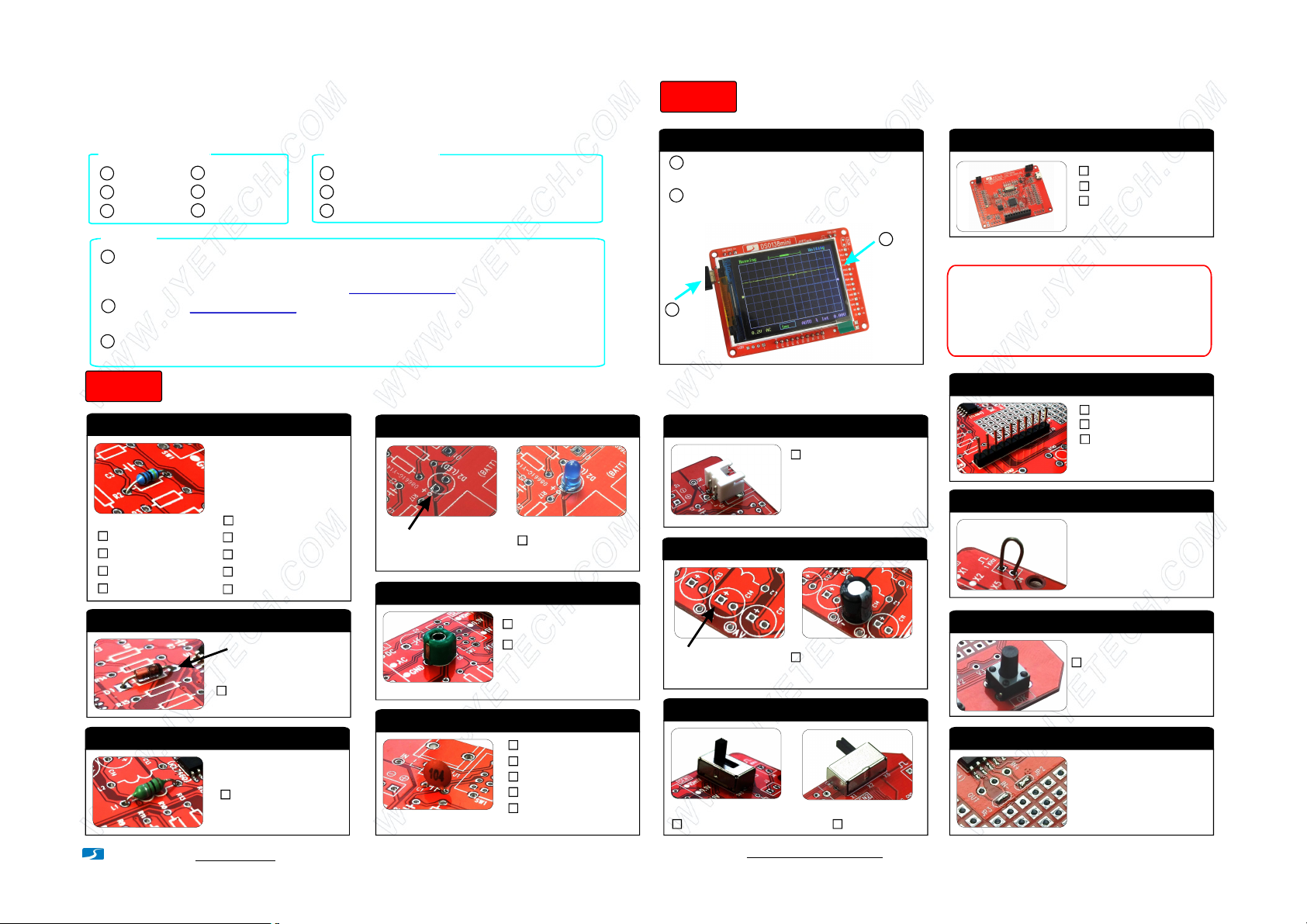
Step 1
Test and Assembly Main Board
1. Check the main board
Before mounting any parts to the main board
1
Use an USB cable with USB-Micro plug to power
the main board through J7.
You should see the scope boots up to a screen
2
similar to the photo below. D1 (LED) should
blink three times during the booting.
1
Apply power
2
Check
display
2. Pin-headers (female)
J4
Attention
Do not solder any parts to the board if
you find problem. Otherwise warranty
will be voided. Report to your vender
or JYE Tech for any problem found.
:
1 X 10 pin
:
1 X 2 pinJ8
:
1 X 3 pinJ9
Step 2
Assembly Analog Board (follow the order as numbered)
1. Resistors
R1, R13
R2
R3, R15
R4
100KΩ
:
:
1.8MΩ
:
200KΩ
2MΩ:
2. Diode
3. HF-Chokes
Note:
Always meter resistor
values before soldering
because color bands are
easy to mis-read.
Resistors are all 1/8W.
R5
R6, R14, R17
R7, R11
R8, R12
R9, R10, R16
:
20KΩ
:
300Ω
:
180Ω
:
120Ω
:
1.1KΩ
Cathode
:
L1,L2
Zener, 2.0V
100Hμ
:
D1
4. LED
Solder positive pole
(the longer lead) to
the square pad
D2
5. Capacitor trimmers
C4
5 - 30pF (green)
:
5 - 30pF (green)[H]
C6
:
2 - 6pF (blue)[J]
6. Ceramic Capacitors
:
0.1F
C1
220pF:
C2
3pF:
C3
1pF [ver. H only]:
C5
:
120pF [H]
C7
500pF [J]
LED, blue,
:
dia. 3mm
μ
7. Pin header
:
2 Pin, 2.54mm,
J1, J6
rightangled
Note:
Do not install J1 if BNC
connector is to be used.
8. Electrolytic capacitors
Solder positive pole
(the longer lead) to
the square pad
C10, C11,
C12, C13,
C14
:
100μ /16VF
9. Slide switches
[ H ]
SW1, SW2, SW3 2P3T
:
[ J ]
SW4
:
DPDT
10. Pin-headers (male)
J5
J2
J3
11. Test signal ring
1 ) Make a small ring with a
lead cut-off.
2 ) Solder the ring to the two
holes of J4 (as shown in
the photo).
12. Tact Switches
BTN1, BTN2,
BTN3, BTN4
13. Jumpers
Short JP2 and JP3with
solder (see photo at left).
Keep JP4, JP5, JP6 (on
the bottom side) open.
JP1 has been pre-shorted.
:
1 X 10 pin
:
1 X 3 pin
:
1 X 2 pin
:
6 X 6 X 9mm
JYETech Ltd.
- www.jyetech.com -
Tech Support: www.jyetech.com/forum
Page 1
Page 2
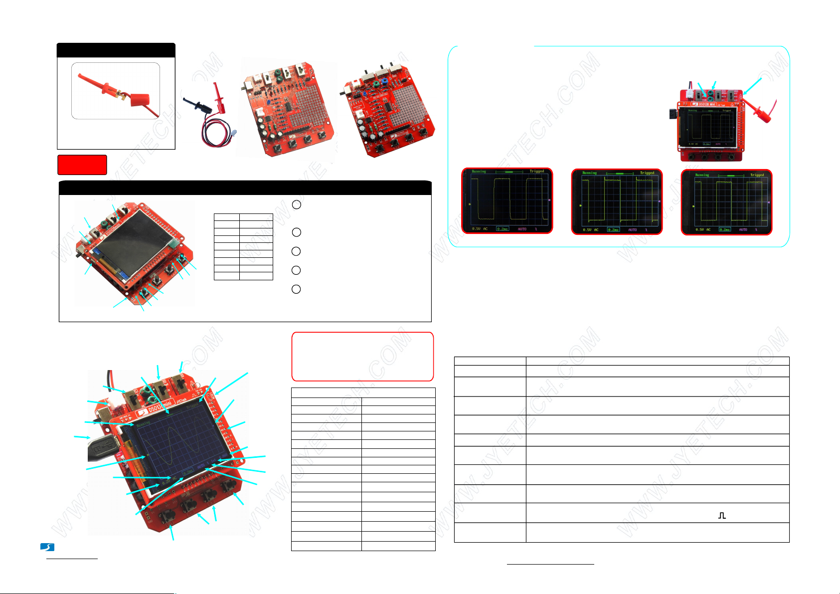
14. Hook Probes
Put wire through hood cap and sold the
wire onto hook terminal as shown.
Match wire color with hook color.
Step 3
Test analog board
1. Check voltages and controls
Couple
Selection
V1
Couple
Sensitivity
(V/div)
Timebase
[SEN1]:
Sensitivity
Selection 1
Horizontal
Position
(s/div)
V+
[Analog board
ver. H shown]
AV+
AV-
V-
[SEL]:
Parameter
Selection
V2
Couple switch
(set to GND)
VBUS
Power input
(USB)
Place negative
pen at GND
Display and Controls
[CPL]:
Signal Input
Oscilloscope
Mode
Power input
Vertical
Position
Indicator
JYETech Ltd.
- www.jyetech.com -
References
(*) Input dependent
VBUS
V+
AV+
VAVV1
V2
V4
V3
V4
V3
Note:
V2 - V4 could have up to
+/- 0.2V variance depending
on power supply voltage.
[Analog board
[SEN2]:
Sensitivity
Selection 2
ver. H shown]
Trigger
State
[+] and [-]:
Parameter
Adjustment
Finished look
+5.10V
(*)
> 3.5V
(*)
> 3.5V
(*)
< -3.5V
(*)
< -3.5V
0V
1.05V
2.1 V
-1.05V
Reset (by shorting
the two pads)
Trigger Level
Indicator
Ext. Trigger In
(PB15)
Trigger Level
(internal only)
Trigger
Source
Trigger
Slope
Trigger
Mode
[OK]:
HOLDRUN/
[H]
Attach the main board to the
1
analog board. Apply 5V DC
power through J7.
2
Set switch [CPL] to GND, [SEN1]
to 1V, and [SEN2] to X5.
Check voltages at the points as
3
shown in the photo.
Check slide switches and push-
4
buttons for correct operation.
Calibrate C4 & C6 if everything
5
is fine (see instructions to the
right).
Attention
1.
Power supply voltage must not exceed
8V.
2.
Allowed maximum signal input voltage
is 50Vpk (100Vpp) .
Specifications
Max realtime sample rate
Analog bandwidth
Sensitivity range
Max input voltage
Input impedance
Resolution
Record length
Timebase range
Trigger modes
Trigger position range
Trigger sources
Ext. trigger thresholds
Ext. trigger input range
Power supply
Current consumption
Dimension
Weight
1MSa/s
0 -- 200KHz
10mV/div - 5V/div
50Vpk (1X probe)
1M ohm/20pF
12 bits
1024 points
500s/Div -- 10us/Div
Auto, Normal, and Single
Center (fixed)
Internal/External
Low: 1.1V, High: 2.2V
0V - 10V(max)
3.5V - 5V DC
< 100mA
85 x 75 x 15 (mm)
50 gram (without probe)
[J]
Calibrating C4 & C6
1.
Insert hook probe to J1. Connect the red hook to the test signal
terminal J4 and leave the black hook un-connected.
2.
Set [SEN1] switch to 0.1V and [SEN2] switch to X5.
Set [CPL] switch to AC or DC.
3.
Adjust timebase to 0.2ms. You should see waveform similar
to that shown in photos below. If traces are not stable adjust
trigger level (the pink triangle on right screen border) so as
you get a stable display.
4.
Turn C4 (capacitor trimmer) with a small screw driver so that
the waveform displays sharp rightangle (photo C).
5.
Set [SEN1] switch to 1V and [SEN2] switch to X1while keep all other
settings unchanged. Adjust C6 so that sharp rightangle waveform is
displayed.
A – Not enough
B – Too much
Operations
[SEL] button:
[+] and [-] button:
[OK] button:
[CPL] switch:
[SEN1]/[SEN2] :
Select parameter to be adjusted. The selected parameter will be highlighted.
Adjust the parameter selected by [SEL] button.
Freeze waveform refresh (entering HOLD state). Press on it again will de-freeze.
Set couple to DC, AC, or GND. When GND is selected the scope input is disconnected
from outside and connected to ground internally (0V input).
Adjust sensitivity. The product of [SEN1] and [SEN2] settings makes the
actual sensitivity which is displayed at the screen lower-left corner.
More Operations
Functions Operations
VPos Alignment
Measurements
ON/OFF
Save Waveform
Recall Waveform
Default Restore
Center HPos
Center Trigger
Level
Send Waveform
Data
Toggle Test Signal
Amplitude
Calibrate Analog
Gain
Tech Support: www.jyetech.com/forum
Move cursor to VPos indicator. Hold down [OK] for 3 seconds. Then follow screen prompts.
Move cursor to timebase. Hold down [OK] button for 3 seconds to turn ON or OFF on-screen
measurements including Vmax, Vmin, Vavr, Vpp, Vrms, Freq., Cycle, Pulse width, and Duty cycle.
Press [SEL] & [+] buttons simultaneously. The currently displayed waveform
will be saved to EEPROM. The existing data in EEPROM will be over-written.
Press [SEL] & [-] buttons simultaneously. Recalled waveform is always displayed
in Hold state.
Hold down [+] and [-] buttons simultaneously for about 3 seconds.
Move cursor to the top bar. Hold down [OK] button for about 3 seconds. This will move
the display window to the center of capture buffer.
Move cursor to trigger level indicator. Hold down [OK] for 3 seconds. This will set
the trigger level to the medium value of signal amplitude.
Hold down [SEL] button for 3 seconds will send waveform data in texts via serial port
J5. The baudrate is 115200. Data format is 8N1.
Move cursor to trigger slope indicator. Hold down [OK] button for 3 seconds to toggle test signal
amplitude between 3.3V and about 0.14V. The amplitude is indicated by to screen top.
Move cursor to trigger source indicator. Hold down [OK] button for 3 seconds to enter analog gain
calibration mode. Follow the on-screen instructions.
Leave black hook
un-connected
Connect red hook to
test signal output
C4C6
C – Good
[Analog board
ver. H shown]
Page 2
 Loading...