

Page 1
DSO DIY Kit
JYETech
WWW.JYETECH.COM
User Manual
Shell
See page 2 for
tools needed
Rev. 07
Applicable models: 15001K, 15002K
Applicable firmware version: 113-15001-061 or later
Before you start
1
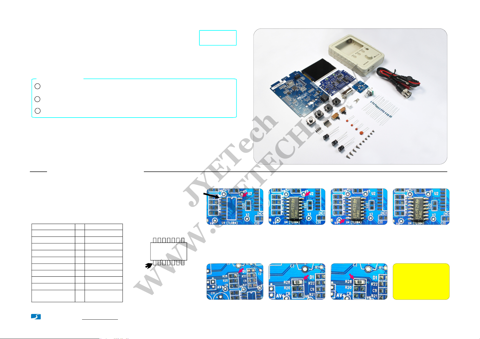
Check kit contents and part quantities/values by the photo at right and part list in page2
and page 3. Report missing or wrong parts to your vendor.
Resistor values are easy to mis-read. It is strongly suggested to check their values
2
by ohm-meter before soldering them to board.
3
Make sure you understand the polarities and orientations of all parts.
Important !!!
If your have purchased 15002K kit (SMD not pre-soldered) you must install all
SMD parts before mounting the through-hole parts. Please refer to the instructions
below for SMD part installation. Otherwise, proceed to page2 to start through-hole
part assembly.
SMD parts are only installed to the analog board (PCB PN# 109-15001-xxx).
How to Solder SMD Parts
1. Before soldering check components against the
part list to make sure you have correct parts.
2. Identify IC orientation and diode polarity (see photos).
3. Do not put iron on one pad for too long time. Otherwise,
traces may peel off and get damaged.
Solder ICs
Pin1
SMD Part Lis
Loc/Ref
U1
U2
U3
U4
U5
U6 1
R19, R20
R17, R18
C3, C5
C9, C12, C13, C14,
C15, C16, C17, C18
(For PCB 109-15001-00F)
Qty Descriptions
1
TL084, SO14
74HC4053, SO16
1
74HC4051, SO16
1
1
78L05, SOT89
1
ICL7660, SO8
79L05, SOT89
2
1K,1%, 0805
2
10K,1%, 0805
2
Cap trimmer, 30pF
8
0.1uF, 50V, 0805
- www.jyetech.com -JYE Tech Ltd.
Identify IC orientation
TL084C
PIN 1
Place IC in front of
you so that its marking
read from left to right.
The first pin at lowerleft corner is pin 1.
Apply solder to a corner
pad
Solder IC to the pad. Make
sure pins are aligned to pads
Solder two-terminal parts
Apply solder to one pad
Solder part to the pad
Solder the pin at the opposite
corner so as chip is fixed
Solder the other pad
Solder all the rest pins one
by one
Note:
Photos here are for
illustration only.
They may not match
the real board.
Page 1
Page 2
Important
JYETech
WWW.JYETECH.COM
If your kit does not have SMD
device pre-soldered you are
strongly suggested to install
all SMD parts before mounting
through-hole parts. Please see
instructions at Page 1.
Tools you need
1
20 - 25W iron for most of parts. For the
BNC connector higher power iron (50 100W) is recommended if available.
Rosin solder wire (0.8 - 1mm dia.)
2
Digital multimeter
3
Screw driver (phillips, size# 0)
4
Flush cutter
5
Tweezers
6
DC 9V power supply with 200mA (or higher)
7
current capacity and 5.5 x 2.1mm plug.
Needle-nose pliers
8
Small slotted screwdriver (2mm width,
9
for cap trimmer adjustment)
Soldering Hints
1
Put leads through mounting holes from the side with
part outline. Ensue component evenly touch PCB.
Solder leads at the other side. Solder should fully
2
fill and cover soldering pads.
Avoid bridges between
neighbering pads.
Cut unused leads
3
flush with cutter.
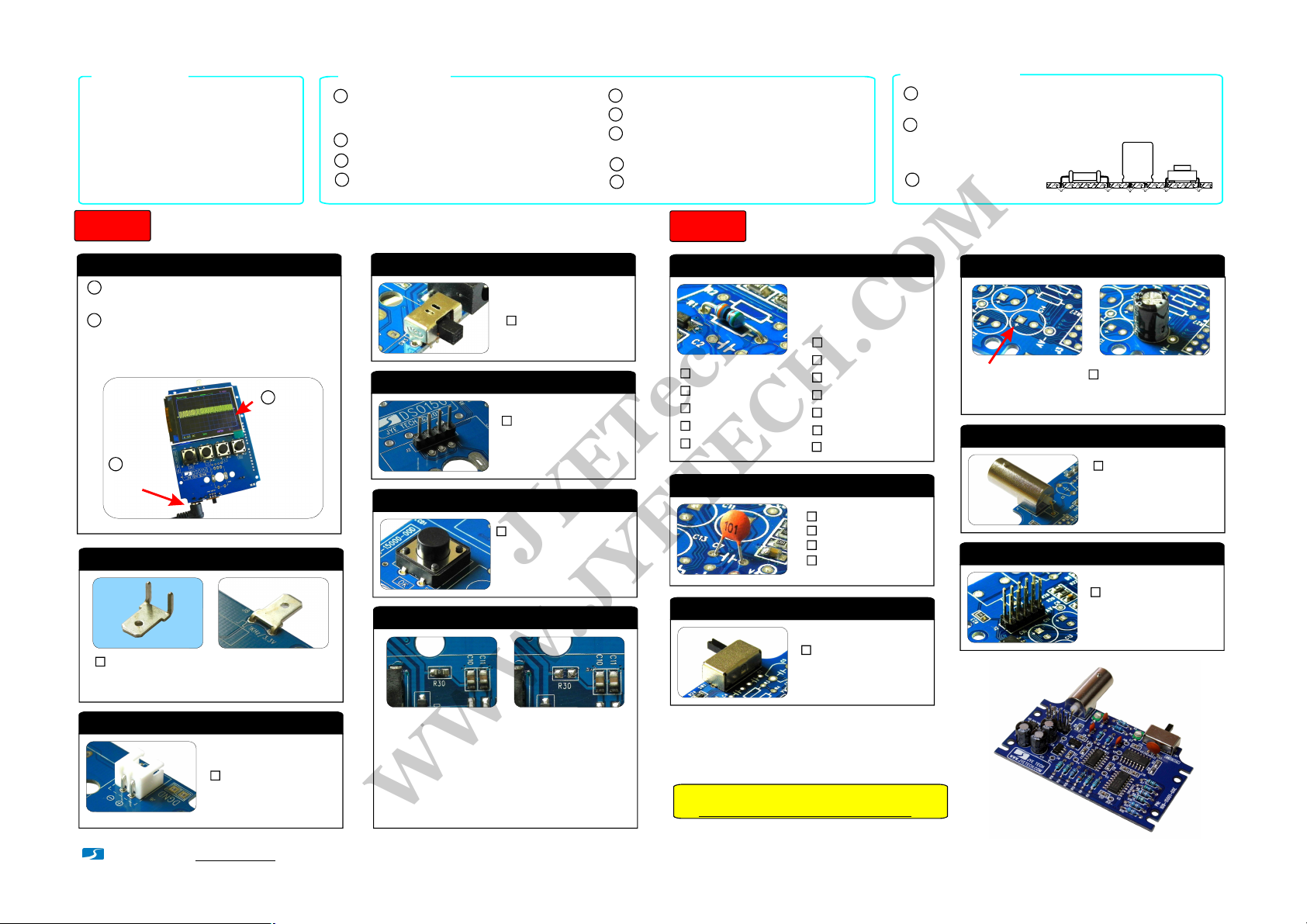
Step 1
Assembly the Main Board (follow the order as numbered)
1. Check the main board
Before mounting any parts to the main board
1
connect a 9V power supply (center positive) to J7
on the board to check the display.
You should see the scope boots up to a screen
2
similar to the photo below. D1 (LED) blinks twice.
Do not solder any parts to the board if you find
problem. Otherwise warranty will be voided.
Report the problem to vender or JYE Tech.
2
Check
display
1
Apply power
(DC jack is 5.5mm dia.
with 2.1mm core)
2. Test Signal Terminal
:
J8
4.8 x 0.8mm terminal
Note:
Before soldering bend the terminal to the
shape as shown in the left photo above.
4. Slide Switch
SW5
5. Pin-header (male)
:
1X4 pin, 0.1" pitch
J2
6. Tact Switches
SW1, SW2,
SW3, SW4
:
7. Remove Resistor R30
:
DPDT
12x12x7mm
Step 2
Assembly the Analog Board (follow the order as numbered)
1. Resistors
Note:
Always meter resistor
values before soldering.
Resistors are all 1/8W.
R7
R1
R2
R3
R4
R5, R6, R14
510KΩ
:
5.1MΩ
:
:
1. Ω2M
11KΩ:
:
1KΩ
R8, R16
R9
R10
R11, R12
R13
R15
2. Ceramic Capacitors
C1
C2
C4
C6
3. Slide switch
SW1
:
300Ω
:
150Ω
91 Ω
:
30 Ω:
15Ω:
3KΩ:
130Ω:
:
0.1F
μ
:
330pF
:
1pF
:
150pF
2P3T
:
4. Electrolytic capacitors
Solder positive pole
(the longer lead) to
the square pad
C8, C10,
C11
:
100μ /16VF
5. BNC connector
BNC
:
J1
Note:
The thicker pins need
to heat up longer to get
good soldering result.
6. Pin-header (male)
J2
:
2 X 5 pin,
2mm pitch
Finished
3. Power Connector (optional)
:
0.1" pitch, rightangle
J6
JYE Tech Ltd.
- www.jyetech.com -
Let iron stay on one pad of the resistor until solder on
the other pad melt and then remove the part.
Note:
R30 is used to bypass SW5 so as the mainboard can be
tested without the power switch. It must be removed
for correct functioning of the power switch.
Now apply power again. Test power switch
and tact buttons for their correct functions.
If you have questions post them
to www.jyetech.com/forum.
Page 2
Page 3
Step 3
JYETech
WWW.JYETECH.COM
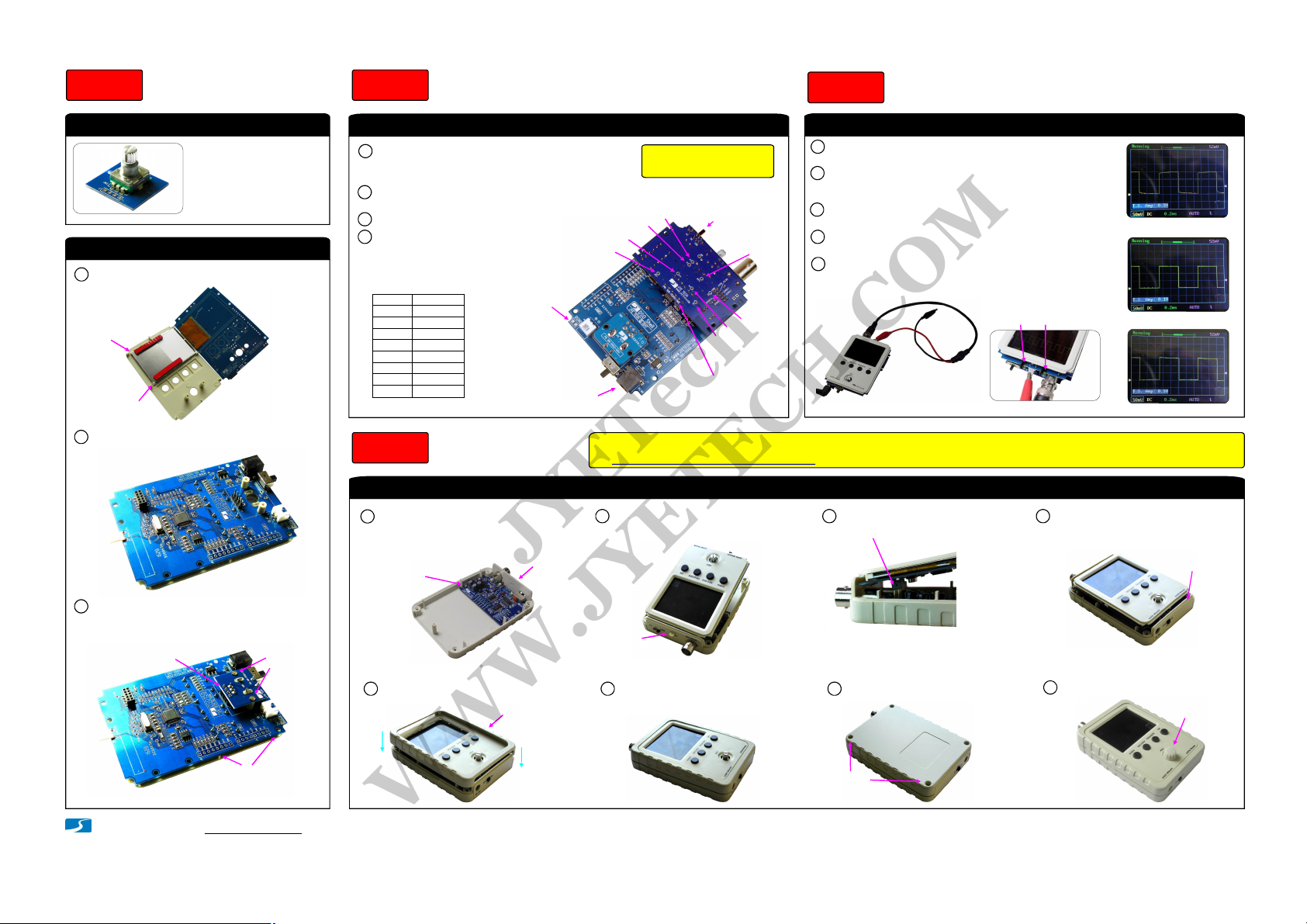
Assembly Front Module
1. Solder Rotary Encoder
Mount to the small PCB
(PN: 109-15002-00A)
Note:
Please pay attention to the
orientation of PCB. Use the
side with outline marking.
2. Assemble Front Module
Fit LCD to front panel as shown below.1
2
Fold the main board over while keeping
LCD in place.
Mount rotary encoder board to the
3
front plate with screws and solder the
board to J2 of the main board.
C. Solder here
Mount with
A.
screws
(KA2x4)
Important !
Step 4
Check Voltages
Always remove power before
connecting or disconnecting
the analog board.
Verify voltages on the analog board
Attach the analog board to the main board
1
by mating J2 on the analog board to J4 on
the main board (see photo).
2
Apply 9V DC power supply to J7 (or J6) on
the main board.
3
Set couple switch to GND position.
Check voltages at the points
4
as shown in the photo.
References
(*) Input dependent
Input
+9.30V
(*)
V+
+8.35V
5.0V+/-2%
AV+
(*)
-7.86V
V-
-5.0V+/-2%
AVV1
0V
V2
0V
V3
0V
V4
~1.65V
Step 6
Put all parts together
Place negative
pen at DGND
Apply power
here
AV-
It is strongly recommended to read the article “FAQ, Tips, and Troubleshooting”
at under the sub-forum “ DSO Shell”.www.jyetech.com/forum
Measurements applicable
for “E ” version PCB
(PN:109-15001-00E)
V1
V3
(DC jack is 5.5mm dia.
with 2.1mm core)
Final assembly
Combine the front module and
Screw the analog board to
1
back cover with the top
bracket attached
Screws
KA2x4
(4 positions)
5
Attach the front frame
Top bracket
Front frame
2
the back cover
Put test signal
terminal through
the small slot
Firmly press the frame in
6
V2
Couple
switch
V+
V4
V-
Analog board
part number
AV+
Tips:
Step 5
Calibration
Perform VPos alignment
before calibrating C3 and C5.
Adjust trimmers C3 and C5
Connect the red clip to the test signal terminal and leave the
1
black clip un-connected (see photo at bottom).
Apply power and boot. Hold down ADJ dial for 3 seconds to
2
bring up Test Signal amplitude display at lower-left corner.
Push ADJ to set the amplitude to 0.1V.
Set sensitivity to 50mV and adjust trigger level so that
3
waveform stable (see “How to Use” at page 4).
Tuning C3 so that sharp rectangle (photo B at left) is obtained.
4
The adjustment for C3 is done.
5
Similarly, for C5 calibration push ADJ to set test signal to
3.3V. Change sensitivity to 1V. Tuning C5 so that sharp
rectangle waveform is obtained. The adjustment is done.
C3
C5
Make sure receptacle (J4)
3
mate with pin-header (J2)
Screw up at the back
7
Attach bottom bracket before
4
holding the two modules
together
Attach knob cap and done!
8
Not enoughA.
GoodB.
Too muchC.
Bottom bracket
Knob cap
Important !
Make sure PCB evenly
JYE Tech Ltd.
B.
touch the front plate
while doing C.
- www.jyetech.com -
Screws
PA2.3x8
(4 positions)
Page 3
Page 4
How to Use
JYETech
WWW.JYETECH.COM
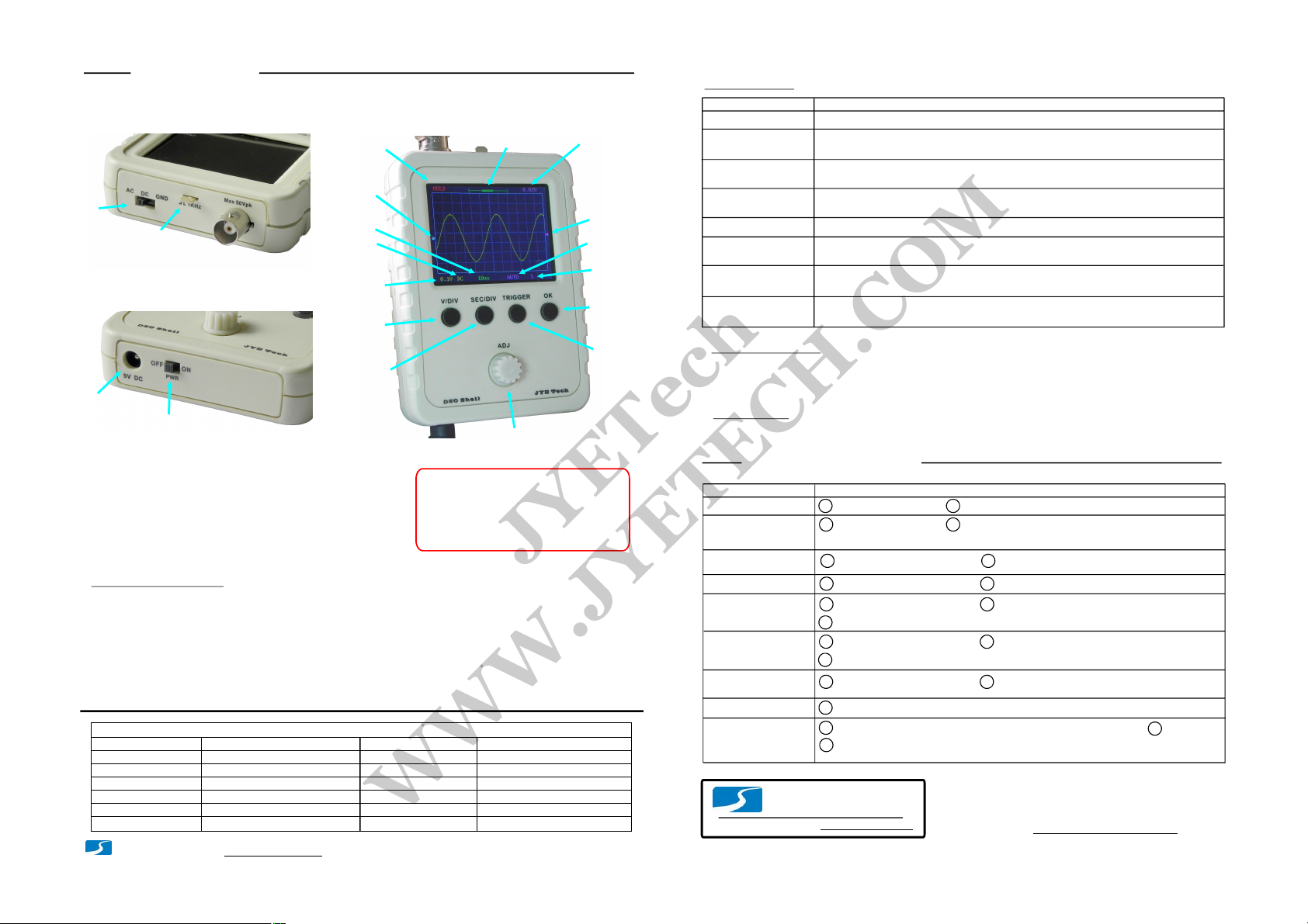
Display and Controls
Oscilloscope
State
Vertical
Position
Couple
Switch
Test Signal
output
Connectors
for Power Supply
(5.5 x 2.1mm)
Power
Switch
BNC
Connector
(Signal Input)
Indicator
Timebase
(s/div)
Couple
Sensitivity
(V/div)
Sensitivity
Button
Timebase
Button
Connections
Power Supply:
Probe:
Connect 9V DC power supply to the 5.5x2.1mm
jack at bottom (center positive). Power supply
voltage must be in the range of 8 - 10V.
Connect probe to the BNC connector at top.
Operations
Basic Button Functions
[V/DIV]:
[SEC/DIV]:
[TRIGGER]:
[OK]:
[ADJ]:
Couple switch:
Specifications
Max realtime sample rate Timebase range
Analog bandwidth
Sensitivity range
Max input voltage
Input impedance
Resolution
Record length
JYE Tech Ltd.
Select sensitivity or vertical position. The selected parameter indicator will be highlighted.
Select timebase or horizontal position. The selected parameter will be highlighted. indicator
Select trigger mode, trigger level, and trigger edge. The selected parameter will be highlighted. indicator
Enter HOLD state (freeze waveform). Press it again will de-freeze.
Adjust the parameter seleted (highlighted). Short press toggles mode.Fast Adjustment
Set couple to DC, AC, or GND. When GND is selected the scope input is isolated from input
signal and connected to ground (0V input).
1MSa/s
0 -- 200KHz
5mV/div - 20V/div
50Vpk (1X probe)
1M ohm/20pF
12 bits
1024 points
- www.jyetech.com -
Attention
1.
Power supply voltage must not exceed
10V. Otherwise it may damage the ICs
inside.
2.
Allowed maximum signal input voltage
is 50Vpk (100Vpp) with the clip probe.
Trigger modes
Trigger position
Power supply
Current consumption
Dimension
Weight
Horizontal
Position
Indicator
Adjustment
Dial
500s/Div -- 10us/Div
Auto, Normal, and Single
Center of buffer
9V DC (8 – 10V)
~120mA @ 9V
105 x 75 x 22mm
100 gram (without probe and PS)
Trigger Level
Readout
(This becomes
trigger state for
firmware version
-055 or later)
Trigger
Level
Indicator
Trigger
Mode
Trigger
Slope
HOLDRUN
Button
Trigger
Button
More Functions
Functions
VPos Alignment
Measurements
ON/OFF
Save Waveform
Recall Waveform
Default Restore
Center HPos
Center Trigger
Level
/
SensitivityButton
Fast Adjustment
About Trigger State
The trigger can have three states including Holdoff, Waiting, and Trigged. They are explained below.
Holdoff:
Waiting:
Trigged:
Trigger is disabled until a portion of sample buffer prior to a trigger point is filled with raw data.
Trigger is waiting for a valid signal slope.
A valid signal slope has been detected and registered.
Operations
Set Couple Switch to GND position. Hold down [V/DIV] button for about 3 seconds.
Hold down [OK] button for about 3 seconds. This will turn ON or OFF on-screen display of
measurements including Vmax, Vmin, Vavr, Vpp, Vrms, Freq., Cycle, Pulse width, and Duty cycle.
Press [ADJ] & [] buttons simultaneously. The currently displayed waveform
will be saved to EEPROM. The existing data in EEPROM will be over-written.
Press [] & [] buttons simultaneously. ADJTrigger Recalled waveform is always displayed
in Hold state.
Hold down [SEC/DIV] and [TRIGGER] buttons simultaneously for about 3 seconds.
Hold down [SEC/DIV] button for about 3 seconds. This will make the data at the center
of capture buffer displayed.
Hold down [TRIGGER] button for about 3 seconds. This will set the trigger level t0 the
medium value of signal amplitude.
Short press of [ADJ] toggles mode on and off for VPos, HPos, and
Trigger Level. A “ >>” sign appearing at top of screen indicates is ON.
SEC/DIV
Fast Adjustment
Fast Adjustment
Rolling Mode
When timebase is set to 50ms or slower and trigger mode is set to AUTO the scope will automatically switch to
Rolling Mode
where waveform shifts from right to left constantly. The trigger is disabled under this mode.
Troubleshooting
Problems Possible Causes
Connector J7 defective.
Bad V+
Bad V-
Bad AV-
Bad AV+
V1 does not close
to 0V
V2 does not close
to 0V
V3 does not close
to 0V
Bad V4
No Trace
JYE Tech Ltd.
Tel. +86-0773-2113856
1 2 Diode D2 open or damaged.
Bad C12 and/or C13.
1
Hint: Check with R27 disconnected would let you know the issue is caused by load or source.
R27 bad soldering or wrong value.
1
R26 bad soldering or wrong value.2Shorts between AV+ and ground.
1
SW1 not set to GND position.
1
Bad soldering on U1.
3
SW1 not set to GND position.
1
Bad soldering on U1.
3
Bad soldering on U1 and/or U2.
1
Bad soldering on R13, R14, and R15.
1
Incorrect V4. If V4 is correct perform factory default restore as described in
1
Make sure trigger mode is AUTO and timebase is 1ms. Hold down [SEC/DIV] and [TRIGGER]
2
buttons simultaneously for 3 seconds.
www.jyetech.com
2 U5 (7660) bad soldering or defective.
Shorts between AV- and ground.
2
Bad soldering on R1 and/or R2.
2
Bad soldering on R3 and/or R4.
2
Bad soldering on R5 and/or R6.
2
2
Tech forum: www.jyetech.com/forum
Page 4
 Loading...