

Page 1

O
S
/
S
S
E
R
C
L
AFN
CH,
7
S
O
R
VI
E MANUA
M
DEL
: XV-N350B
XV-N352
DVD-VIDE
PLAYE
MODELS : XV-N350B/XV-N352
P/NO :
31629394MAR
200
Page 2

CONTENTS
SECTION 1.........SUMMARY
SECTION 2.........CABINET & MAIN CHASSIS
SECTION 3.........ELECTRICAL
SECTION 4.........MECHANISM (DP-11)
SECTION 5.........REPLACEMENT PARTS LIST
Page 3

SECTION 1
SUMMARY
CONTENTS
PRODUCT SAFETY SERVICING GUIDELINES FOR DVD PRODUCTS..................................1-3
SERVICING PRECAUTIONS....................................................................................................................1-4
• GENERAL SERVICING PRECAUTIONS
• INSULATION CHECKING PRODEDURE
• ELECTROSTATICALLY SENSITIVE (ES) DEVICES
SERVICE INFORMATION FOR EEPROM ...........................................................................................1-5
SPECIFICATIONS ........................................................................................................................................1-6
1-2
Page 4
PRODUCT SAFETY SERVICING GUIDELINES FOR DVD PRODUCTS
IMPORTANT SAFETY NOTICE
This manual was prepared for use only by properly trained audio-video service
technicians.
When servicing this product, under no circumstances should the original design be
modified or altered without permission from JVC. All components should be replaced
only with types identical to those in the original circuit and their physical location, wiring
and lead dress must conform to original layout upon completion of repairs.
Special components are also used to prevent x-radiation, shock and fire hazard.
These components are indicated by the letter “x” included in their component
designators and are required to maintain safe performance. No deviations are
allowed without prior approval by LG Corporation.
Circuit diagrams may occasionally differ from the actual circuit used. This way,
implementation of the latest safety and performance improvement changes into the
set are not delayed until the new service literature is printed.
CAUTION
customized installations without manufacturer’s approval. Unauthorized
modifications will not only void the warranty, but may lead to property damage or user
injury.
Service work should be performed only after you are thoroughly familiar with these
safety checks and servicing guidelines.
GRAPHIC SYMBOLS
SERVICE INFORMATION
While servicing, use an isolation transformer for protection from AC line shock. After
the original service problem has been corrected, make a check of the following:
FIRE AND SHOCK HAZARD
1. Be sure that all components are positioned to avoid a possibility of adjacent
2. Verify that all protective devices such as insulators, barriers, covers, shields, strain
3. Soldering must be inspected to discover possible cold solder joints, solder
4. Check for physical evidence of damage or deterioration to parts and components,
5. No lead or component should touch a high current device or a resistor rated at 1
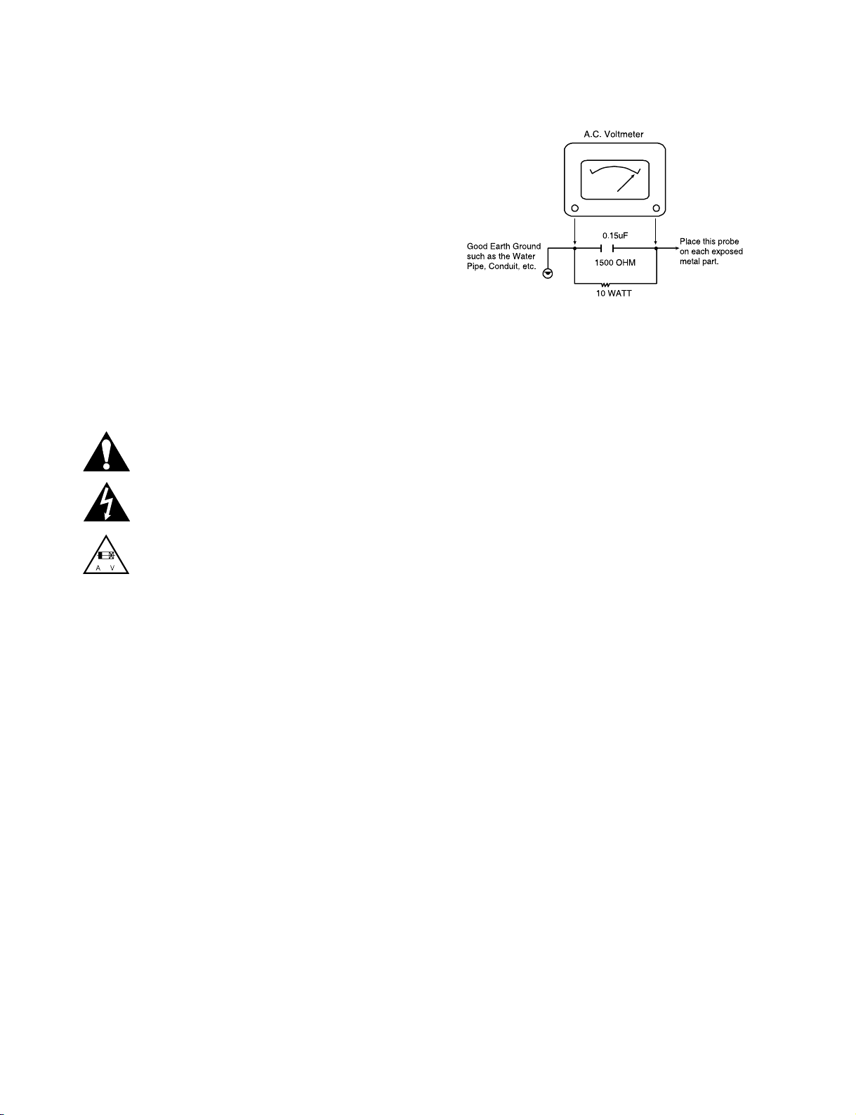
6. After reassembly of the set, always perform an AC leakage test on all exposed
: Do not attempt to modify this product in any way. Never perform
The exclamation point within an equilateral triangle is intended to alert
the service personnel to important safety information in the service
literature.
The lightning flash with arrowhead symbol within an equilateral
triangle is intended to alert the service personnel to the presence of
noninsulated “dangerous voltage” that may be of sufficient magnitude
to constitute a risk of electric shock.
The pictorial representation of a fuse and its rating within an equilateral
triangle is intended to convey to the service personnel the following
fuse replacement caution notice:
CAUTION: FOR CONTINUED PROTECTION AGAINST RISK OF
FIRE, REPLACE ALL FUSES WITH THE SAME TYPE AND
RATING AS MARKED NEAR EACH FUSE.
component shorts. This is especially important on items trans-ported to and from
the repair shop.
reliefs, power supply cords, and other hardware have been reinstalled per the
original design. Be sure that the safety purpose of the polarized line plug has not
been defeated.
splashes, or sharp solder points. Be certain to remove all loose foreign particles.
for frayed leads or damaged insulation (including the AC cord), and replace if
necessary.
watt or more. Lead tension around protruding metal surfaces must be avoided.
metallic parts of the cabinet (the channel selector knobs, antenna terminals,
handle and screws) to be sure that set is safe to operate without danger of
electrical shock. DO NOT USE A LINE ISOLATION TRANSFORMER DURING
THIS TEST. Use an AC voltmeter having 5000 ohms per volt or more sensitivity
in the following manner: Connect a 1500 ohm, 10 watt resistor, paralleled by a .15
mfd 150V AC type capacitor between a known good earth ground water pipe,
conduit, etc.) and the exposed metallic parts, one at a time. Measure the AC
voltage across the combination of 1500 ohm resistor and .15 mfd capacitor.
Reverse the AC plug by using a non-polarized adaptor and repeat AC voltage
measurements for each exposed metallic part. Voltage measured must not
exceed 0.75 volts RMS. This corresponds to 0.5 milliamp AC. Any value
exceeding this limit constitutes a potential shock hazard and must be corrected
immediately.
TIPS ON PROPER INSTALLATION
1. Never install any receiver in a closed-in recess, cubbyhole, or closely fitting shelf
space over, or close to, a heat duct, or in the path of heated air flow.
2. Avoid conditions of high humidity such as: outdoor patio installations where dew
is a factor, near steam radiators where steam leakage is a factor, etc.
3. Avoid placement where draperies may obstruct venting. The customer should also
avoid the use of decorative scarves or other coverings that might obstruct
ventilation.
4. Wall- and shelf-mounted installations using a commercial mounting kit must follow
the factory-approved mounting instructions. A product mounted to a shelf or
platform must retain its original feet (or the equivalent thickness in spacers) to
provide adequate air flow across the bottom. Bolts or screws used for fasteners
must not touch any parts or wiring. Perform leakage tests on customized
installations.
5. Caution customers against mounting a product on a sloping shelf or in a tilted
position, unless the receiver is properly secured.
6. A product on a roll-about cart should be stable in its mounting to the cart.
Caution the customer on the hazards of trying to roll a cart with small casters
across thresholds or deep pile carpets.
7. Caution customers against using extension cords. Explain that a forest of
extensions, sprouting from a single outlet, can lead to disastrous consequences to
home and family.
1-3
Page 5

SERVICING PRECAUTIONS
CAUTION: Before servicing the DVD covered by this service
data and its supplements and addends, read and follow the
SAFETY PRECAUTIONS. NOTE: if unforeseen circumstances
create conflict between the following servicing precautions
and any of the safety precautions in this publication, always
follow the safety precautions.
Remember Safety First :
General Servicing Precautions
1.Always unplug the DVD AC power cord from the AC power
source before:
(1) Removing or reinstalling any component, circuit board,
module, or any other assembly.
(2) Disconnecting or reconnecting any internal electrical
plug or other electrical connection.
(3) Connecting a test substitute in parallel with an
electrolytic capacitor.
Caution: A wrong part substitution or incorrect polarity
installation of electrolytic capacitors may result in an
explosion hazard.
2.Do not spray chemicals on or near this DVD or any of its
assemblies.
3.Unless specified otherwise in this service data, clean
electrical contacts by applying an appropriate contact
cleaning solution to the contacts with a pipe cleaner,
cotton-tipped swab, or comparable soft applicator.
Unless specified otherwise in this service data, lubrication
of contacts is not required.
4.Do not defeat any plug/socket B+ voltage interlocks with
which instruments covered by this service manual might
be equipped.
5.Do not apply AC power to this DVD and / or any of its
electrical assemblies unless all solid state device heat
sinks are correctly installed.
6.Always connect the test instrument ground lead to an
appropriate ground before connecting the test instrument
positive lead. Always remove the test instrument ground
lead last.
Insulation Checking Procedure
Disconnect the attachment plug from the AC outlet and turn
the power on. Connect an insulation resistance meter (500V)
to the blades of the attachment plug. The insulation
resistance between each blade of the attachment plug and
accessible conductive parts (Note 1) should be more than
1Mohm.
Note 1: Accessible Conductive Parts include Metal panels,
Input terminals, Earphone jacks,etc.
Electrostatically Sensitive (ES) Devices
Some semiconductor (solid state) devices can be damaged
easily by static electricity. Such components commonly are
called Electrostatically Sensitive (ES) Devices. Examples of
typical ES devices are integrated circuits and some field
effect transistors and semiconductor chip components.
The following techniques should be used to help reduce the
incidence of component damage caused by static electricity.
1.Immediately before handling any semiconductor
component or semiconductor-equipped assembly, drain off
any electrostatic charge on your body by touching a known
earth ground. Alternatively, obtain and wear a
commercially available discharging wrist strap device,
which should be removed for potential shock reasons prior
to applying power to the unit under test.
2.After removing an electrical assembly equipped with ES
devices, place the assembly on a conductive surface such
as aluminum foil, to prevent electrostatic charge buildup or
exposure of the assembly.
3.Use only a grounded-tip soldering iron to solder or
unsolder ES devices.
4.Use only an anti-static solder removal device. Some solder
removal devices not classified as “anti-static” can generate
electrical charges sufficient to damage ES devices.
5.Do not use freon-propelled chemicals. These can generate
an electrical charge sufficient to damage ES devices.
6.Do not remove a replacement ES device from its
protective package until immediately before you are ready
to install it. (Most replacement ES devices are packaged
with leads electrically shorted together by conductive
foam, aluminum foil, or comparable conductive material).
7.Immediately before removing the protective material from
the leads of a replacement ES device, touch the protective
material to the chassis or circuit assembly into which the
device will be installed.
Caution: Be sure no power is applied to the chassis or
circuit, and observe all other safety precautions.
8.Minimize bodily motions when handling unpackaged
replacement ES devices. (Normally harmless motion such
as the brushing together of your clothes fabric or the lifting
of your foot from a carpeted floor can generate static
electricity sufficient to damage an ES device.)
1-4
Page 6
SERVICE INFORMATION FOR EEPROM
POWER ON
DVD LOGO Status (NO Disk status)
Remotecontrol
Pause key-->1-->4-->7-->2 in order.
Press number 0~8, Press charater
A~F (1~6 for a while)
Use arrow key (F D G E) to move
to approprite position and make
changes
Press pause key once
DETECT NEW EEPROM
(OPTION EDIT SCREEN)
MODEL: XV-N350B/XV-N352S
NAME HEX
OPT 1 00
OPT 2 00
OPT 3 00
OPT 4 00
OPT 5 00
OPT 6 00
OPT 7 00
OPT 8 00
Change will be applied when power
OFF-->ON.
1-5
Page 7
SPECIFICATIONS
• GENERAL
Power requirements : AC 200 ~ 240V, 50/60Hz
Power consumption : 8W
Dimensions (Approx.) : 430 x 35 x 202mm (17 x 1.4 x 7.9inches)
(W x H x D) without foot
Net Weight (Approx.) : 1.6kg (3.5lbs)
Operating temperature : 5°C to 35°C (41°F to 95°F)
Operating humidity : 5% to 90%
• OUTPUTS
VIDEO OUT : 1.0V(p-p), 75Ω, sync negative, RCA jack x 1 / SCART (TO TV)
AUDIO OUT : 2.0Vrms (1KHz, 0dB), 600Ω, RCA jack (L, R) x 1 / SCART (TO TV)
DIGITAL OUT (COAXIAL) : 0.5V(p-p), 75Ω, RCA jack x 1
SCART Model only
• SYSTEM
Laser : Semiconductor laser, wavelength 650nm
Signal system : PAL / NTSC
Frequency response : DVD (PCM 96 kHz) : 8Hz to 44kHz
DVD (PCM 48 kHz) : 8Hz to 22kHz
CD : 8Hz to 20kHz
Signal-to-noise ratio : More than 90dB (ANALOG OUT connectors only)
Harmonic distortion : Less than 0.02%
Dynamic range : More than 95dB (DVD/CD)
Accessories : Video cable (1), Audio cable (1), Remote control (1), Batteries (2)
1-6
Page 8

SECTION 2
CABINET & MAIN CHASSIS
CONTENTS
EXPLODED VIEWS .....................................................................................................................................2-2
1. CABINET AND MAIN FRAME SECTION ..................................................................................................2-2
2. DECK MECHANISM SECTION (DP-11) ...................................................................................................2-3
3. PACKING ACCESSORY SECTION...........................................................................................................2-4
2-1
Page 9
OPTIONAL PART
C
B
462
460
460
460
250
462
A44
A
300
A26
283
261
261
260
262
320
467
465
261
D
A
C
B
462
462
A48
A46
P101
A47
MAIN
SMPS
5.1CH
SCART
452
D
A43
A49
CABLE1
CN903
452
280
KEY
TIMER
452
A42
EXPLODED VIEWS
1. CABINET AND MAIN FRAME SECTION
2-2
Page 10
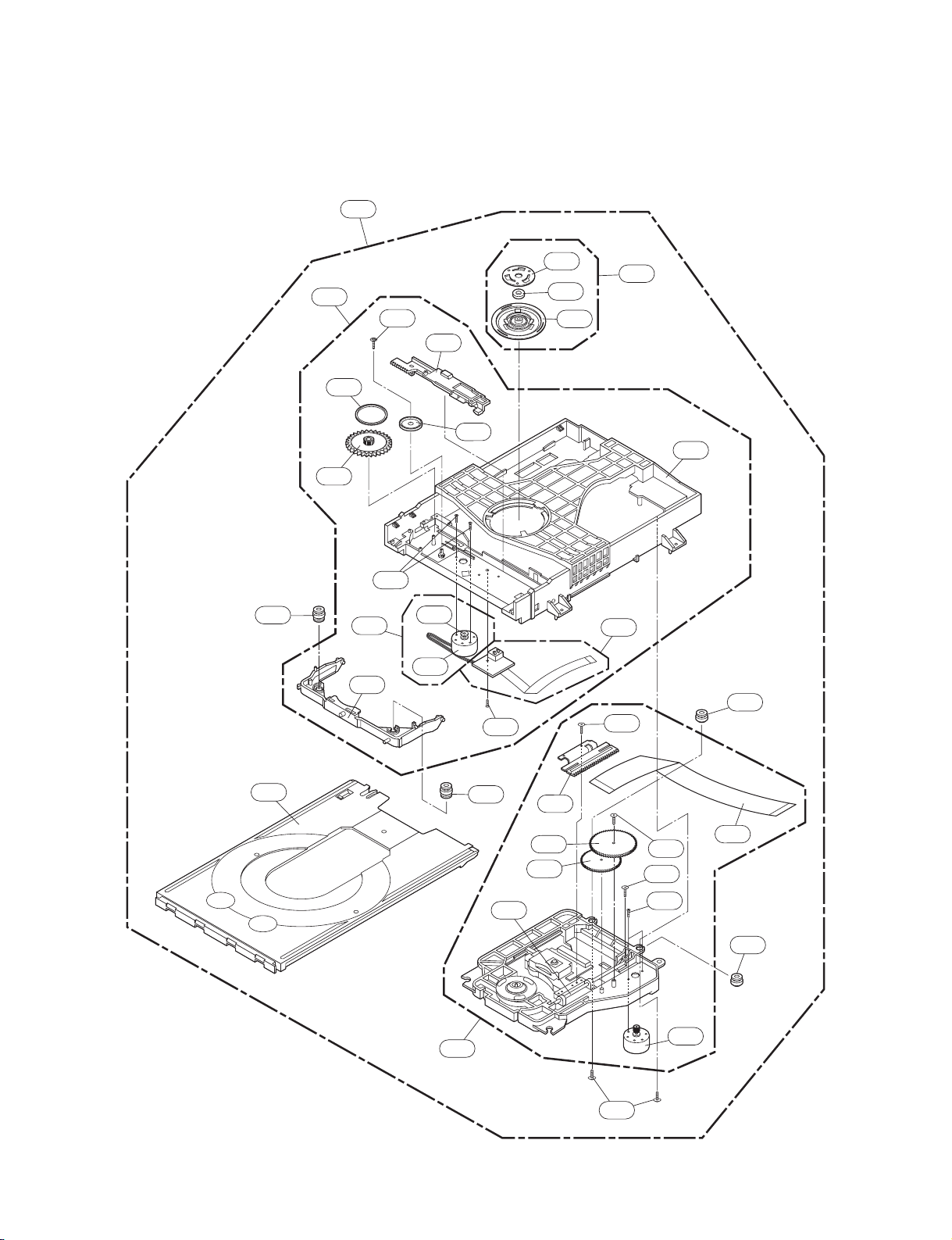
2. DECK MECHANISM SECTION (DP-11)
A26
A02
439
018
013
017
014
001
002
003
020
016
015B
015A
435
015
019
440
432
012A
010
439
431
435
030
024
025
036
A03
430
021
012A
012
012
026
A01
2-3
Page 11
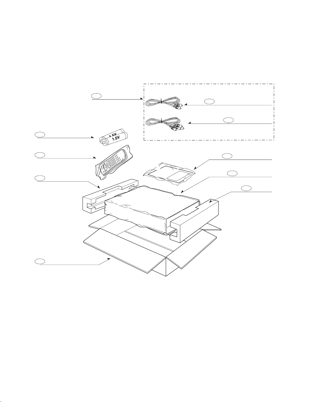
3. PACKING ACCESSORY SECTION
808 BATTERY
810 CABLE SET ASS’Y
811 PLUG ASS’Y 1WAY(YELLOW)
812 PLUG ASS’Y 2WAY
801 OWNER’S MANUAL
804 PACKING SHEET
803 PACKING
900 REMOCON
803 PACKING
802 BOX CARTON
2-4
Page 12

SECTION 3
ELECTRICAL
CONTENTS
ELECTRICAL TROUBLESHOOTING GUIDE.....................................................................................3-2
1. POWER CHECK FLOW ..........................................................................................................................3-2
2. SYSTEM OPERATION FLOW.................................................................................................................3-3
3. SYSTEM TEST FLOW.............................................................................................................................3-4
DETAILS AND WAVEFORMS ON SYSTEM TEST AND DEBUGGING
1. SYSTEM 27MHZ CLOCK, RESET, FLASH R/W SIGNAL....................................................................3-10
2. SDRAM CLOCK.....................................................................................................................................3-12
3. TRAY OPEN/CLOSE SIGNAL ...............................................................................................................3-12
4. SLED CONTROL RELATED SIGNAL (NO DISC CONDITION)............................................................3-13
5. LENS CONTROL RELATED SIGNAL (NO DISC CONDITION) ..........................................................3-13
6. LASER POWER CONTROL RELATED SIGNAL (NO DISC CONDITION) ..........................................3-14
7. SPINDLE CONTROL WAVEFORM (NO DISC CONDITION) ...............................................................3-14
8. FOCUS ON WAVEFORM......................................................................................................................3-15
9. RACKING CONTROL RELATED SIGNAL (SYSTEM CHECKING) ......................................................3-16
10. ZR966 AUDIO COAXIAL OUTPUT (SPDIF) .........................................................................................3-17
11. ZR966 VIDEO OUTPUT WAVEFORM...................................................................................................3-17
12. AUDIO OUTPUT FROM ZR966 ............................................................................................................3-18
CONNECTOR PICTURE ..........................................................................................................................3-19
1. ALL CONNECTOR PICTURE ................................................................................................................3-19
2. P2201 CONNECTOR PICTURE............................................................................................................3-20
3. P2202 CONNECTOR PICTURE............................................................................................................3-20
4. PW6101 CONNECTOR PICTURE ........................................................................................................3-21
5. P6501 CONNECTOR PICTURE............................................................................................................3-21
6. P6602 CONNECTOR PICTURE............................................................................................................3-22
7. P6901 CONNECTOR PICTURE............................................................................................................3-22
8. P7301 CONNECTOR PICTURE............................................................................................................3-23
BLOCK DIAGRAMS ..................................................................................................................................3-24
1. OVERALL BLOCK DIAGRAM ...............................................................................................................3-24
2. POWER SUPPLY BLOCK DIAGRAM ...................................................................................................3-25
3. SERVO BLOCK DIAGRAM ...................................................................................................................3-26
4. MPEG & MEMORY BLOCK DIAGRAM.................................................................................................3-27
5. VIDEO BLOCK DIAGRAM.....................................................................................................................3-28
6. AUDIO BLOCK DIAGRAM.....................................................................................................................3-29
CIRCUIT DIAGRAMS................................................................................................................................3-31
1. POWER (SMPS) CIRCUIT DIAGRAM ..................................................................................................3-31
2. SYSTEM (MPEG) CIRCUIT DIAGRAM.................................................................................................3-33
3. SERVO CIRCUIT DIAGRAM.................................................................................................................3-35
4. AV/JACK CIRCUIT DIAGRAM ...............................................................................................................3-37
5. TIMER/KEY CIRCUIT DIAGRAM ..........................................................................................................3-39
CIRCUIT VOLTAGE CHART...................................................................................................................3-41
PRINTED CIRCUIT BOARD DIAGRAMS...........................................................................................3-43
1. MAIN P.C.BOARD..................................................................................................................................3-43
2. KEY P.C.BOARD ...................................................................................................................................3-45
3. TIMER P.C.BOARD ...............................................................................................................................3-45
4. SMPS P.C.BOARD ................................................................................................................................3-47
5. SCART P.C.BOARD (SCART MODEL ONLY).......................................................................................3-47
.........................................3-10
3-1
Page 13
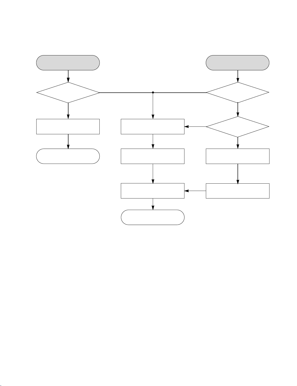
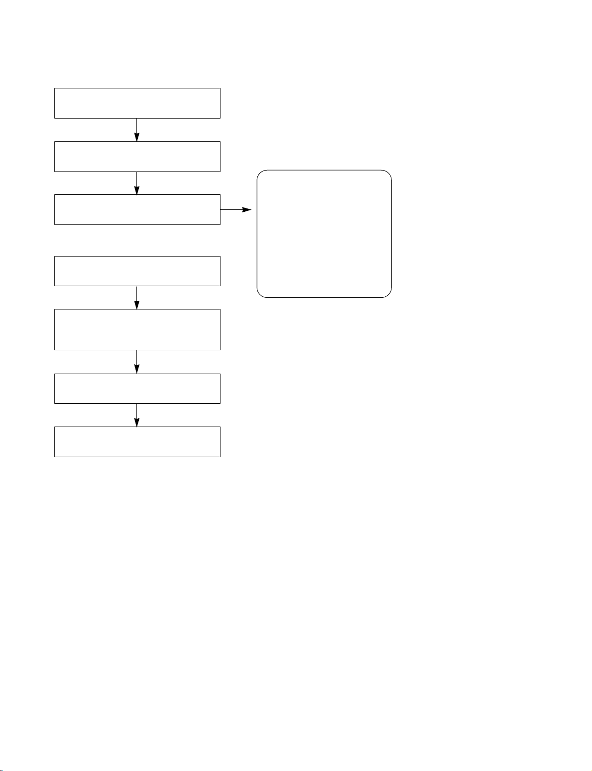
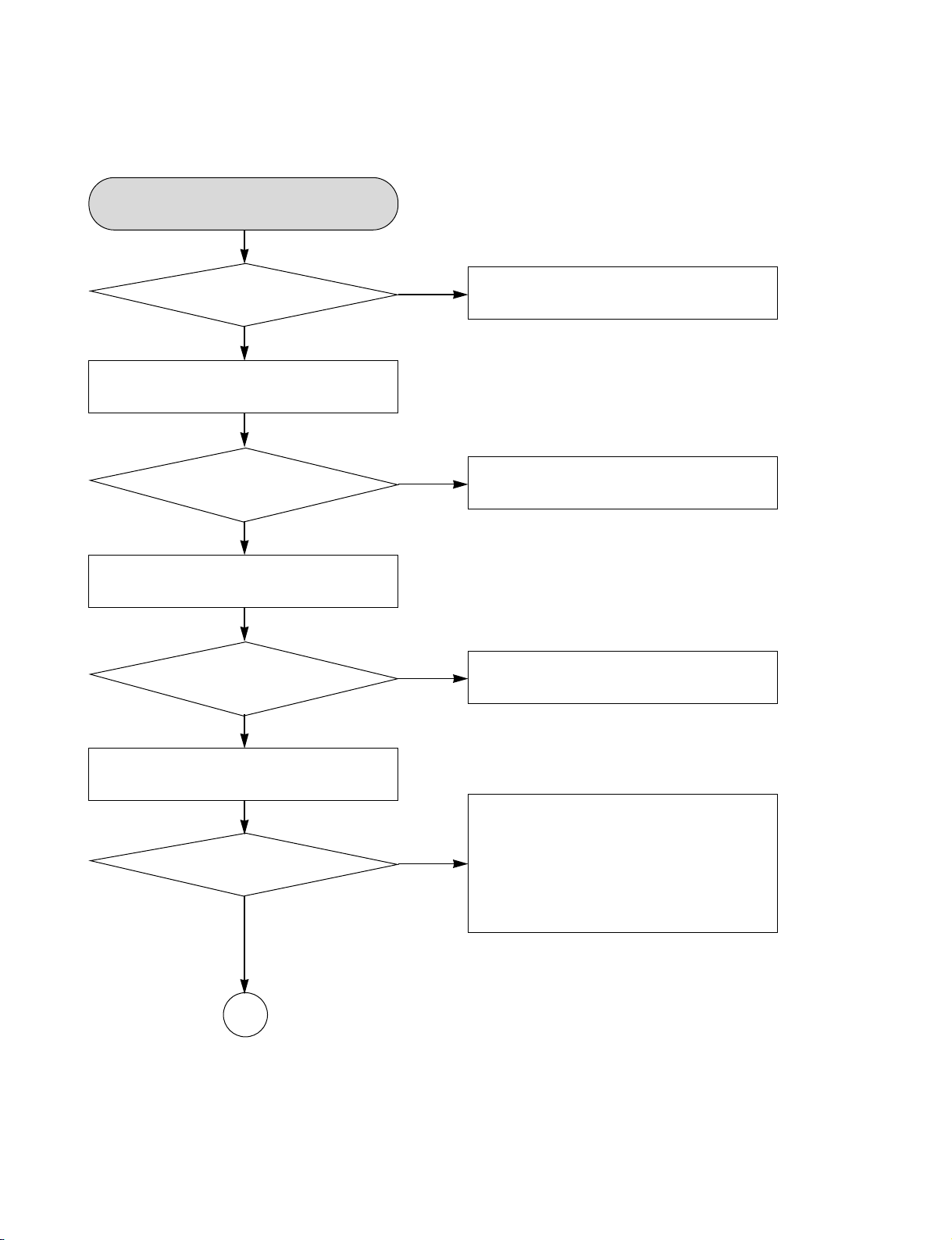
ELECTRICAL TROUBLESHOOTING GUIDE
1. POWER CHECK FLOW
A. B.
No 5V No 3.3VA.
Is 3.3VA
section working?
YES
Is 5.6V present at
collector of Q126?
YES
Replace Q126. Check FR101 Replace Q121.
NO
No 3.3VA
Is there a DC voltage at
cathode of D105 or D107?
NO
NO
NO
Is 3.3VA
section working?
YES
Is 3.3V
present at emitter
of Q121?
YES
YES
Check D105/D106/D107/
D108 and replace.
YES
Replace IC101.
3-2
Page 14
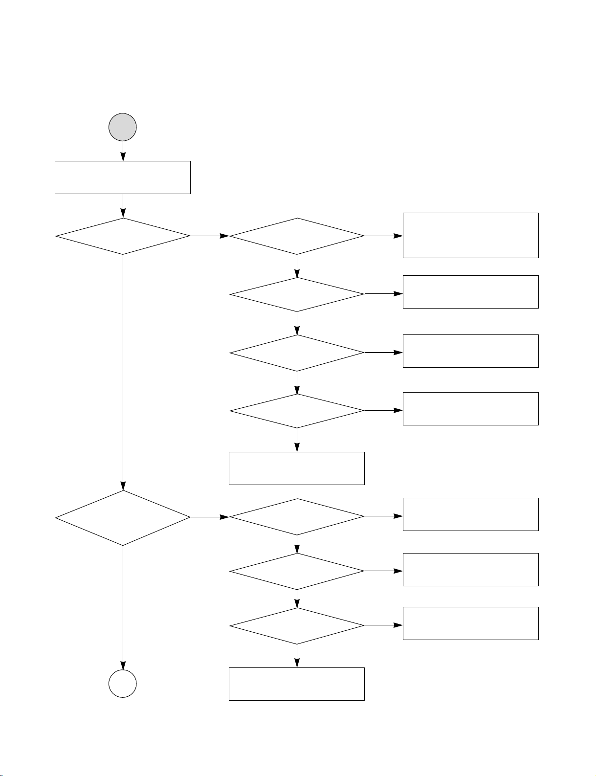
ELECTRICAL TROUBLESHOOTING GUIDE
2. SYSTEM OPERATION FLOW
Power on
1. 8032 initializes SERVO,DSP & RISC registers
2. Write RISC code to SDRAM
3. Reset RISC
Show LOGO
YES
Tray close to closed position
SLED moves to inner position
1. Judge whether have disc and disc type
2. Jump to related disc reading procedure
Recieve OPEN/CLOSE Key?
Tray closed ?
NO
SLED at inner side ?
NO
YES
YES
NO
1. Execute pressed Key & IR key
2. System operation routine loop
1. Stop playback & open Tray
2. Display tray open message & LOGO
NO
Receive CLOSE Key?
YES
3-3
Page 15
ELECTRICAL TROUBLESHOOTING GUIDE
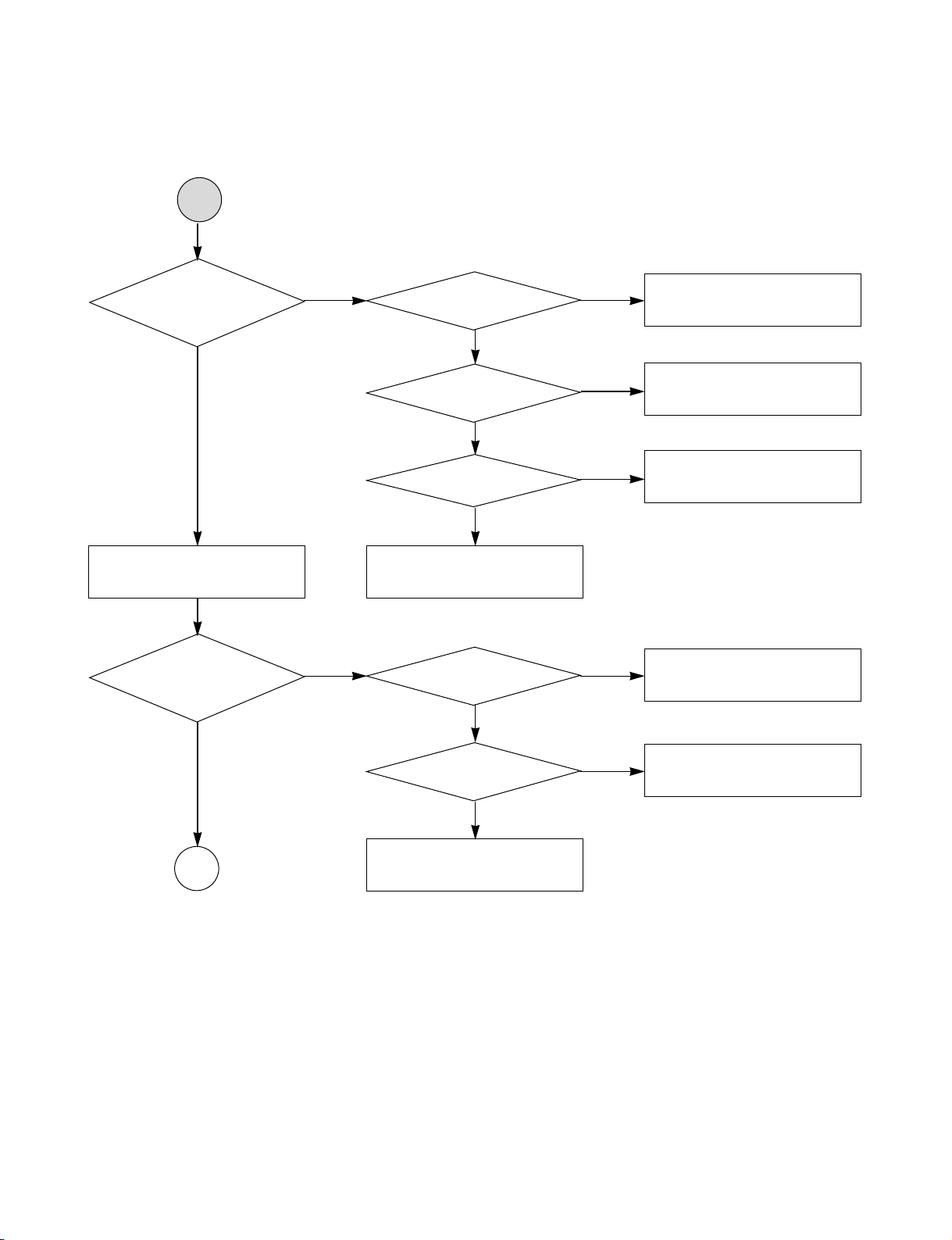
3. SYSTEM TEST FLOW
TEST
Check the AC
Voltage Power PCBA (110V
or 220V)
YES
Switch on the power PCBA
Is the DC
voltage outputs OK?
(5V, 3.3V, 12V, 5.6V
MOTOR)
YES
Make sure the main PCBA don't
short on VCCs and switch it on.
YES
Is 3.3V
and 1.8V DC outputs normal
on main PCBA?
YES
NO
NO
NO
Replace power PCBA or AC transformer.
Repair or Replace power PCBA
Check the regulators or related diodes.
Connect to PC RS232 cable and
update the FLASH memory code.
Update FLASH
successfully?
YES
A
NO
1. Check 27MHz system clock.
2. Check system reset circuit.
3. Check FLASH R/W enable signal PRD,
RWR.
4. Check RS232 SIGNALS.
5. Check FLASH Memory related circuit.
3-4
Page 16
ELECTRICAL TROUBLESHOOTING GUIDE
A
RESET or power on.
Show LOGO?
YES
Does
Tray move inside
when it is not at closed
position?
NO NO
Flash
memory operates
properly?
YES
SDRAM
NO
works properly?
YES
ZR966
VIDEO outputs
NO
properly?
YES
Have TV
NO
signal output?
YES
Check AV cable
connection to TV set.
NO
Normal
TROUT & TRIN
NO
signals?
YES
Check connection lines
between FLASH & ZR966
and the FLASH access time
whether is suitable or not.
Check connection lines
between SDRAM & ZR966
and the SDRAM is damaged.
Check the related
circuit of ZR966.
Check the filtering and amp
circuit of TV signal.
Check the load OPEN &
CLOSE switch
B
YES
Normal
TRCLOSE & TROPEN
signal?
YES
Normal LOAD+ &
LOAD signal?
YES
Check the cable connection
between main PCBA and loader.
3-5
NO
NO
Check the Tray control IO
pins on ZR966 & AM5890S.
Check the Tray control
amplifying circuit on motor driver.
Page 17
ELECTRICAL TROUBLESHOOTING GUIDE
B
Does
the SLED move
to inner side when it is
at outter position?
YES
Do not put in disc and
tray close.
Optical Lens has
movements for searching
focus?
Motor
Driver DRVSB Pin
is high?
YES
Is sled_s
DC Level higher than
1.4V?
YES
SL+ and
SL- output properly?
YES
Check the cable connection
with MECHA.
Proper
focus_s outputs to motor
driver?
YES
NONO
NO
NO
NONO
Check the connection line
of DRVSB signal.
Check the related
circuit of Sled_s.
Check the amp circuit on
motor driver.
Check focus_s connection
on ZR966 and motor dirver.
C
YES
Proper F+ &
F- outputs?
YES
Check cable connect on
with pick-up head.
3-6
NO
Check the amp circuit on
motor dirver.
Page 18
ELECTRICAL TROUBLESHOOTING GUIDE
C
Laser
turns on when reading
disc?
YES
Put disc in?
YES
Disc ID is correct?
NO NO
DVD_LD,
CD_LD output properly?
YES
Collector
NO
voltage of power transistor
is OK?
YES
Check cable connection
between transistor ouput
and pick-up head.
NO
Laser off
NO
Proper RF signal
NO
on OPU
YES
Check the laser power circuit
on ZR966 and connecting to
power transistor.
Check the related circuit on
laser power transistor
Check the related circuit
on RF signal.
YES
Does spindle rotate?Does spindle rotate?
YES
D
Check DVD_LD &
CD_LD signal
NO NO
Proper spindle_s
signal on ZR966
YES
SP+ & SP- output properly?
YES
NO
Check the cable connection
between spindle and main
PCBA.
3-7
Check spindle_s related
circuit on ZR966.
Check the spindle control
amp circuit of motor driver.
Page 19

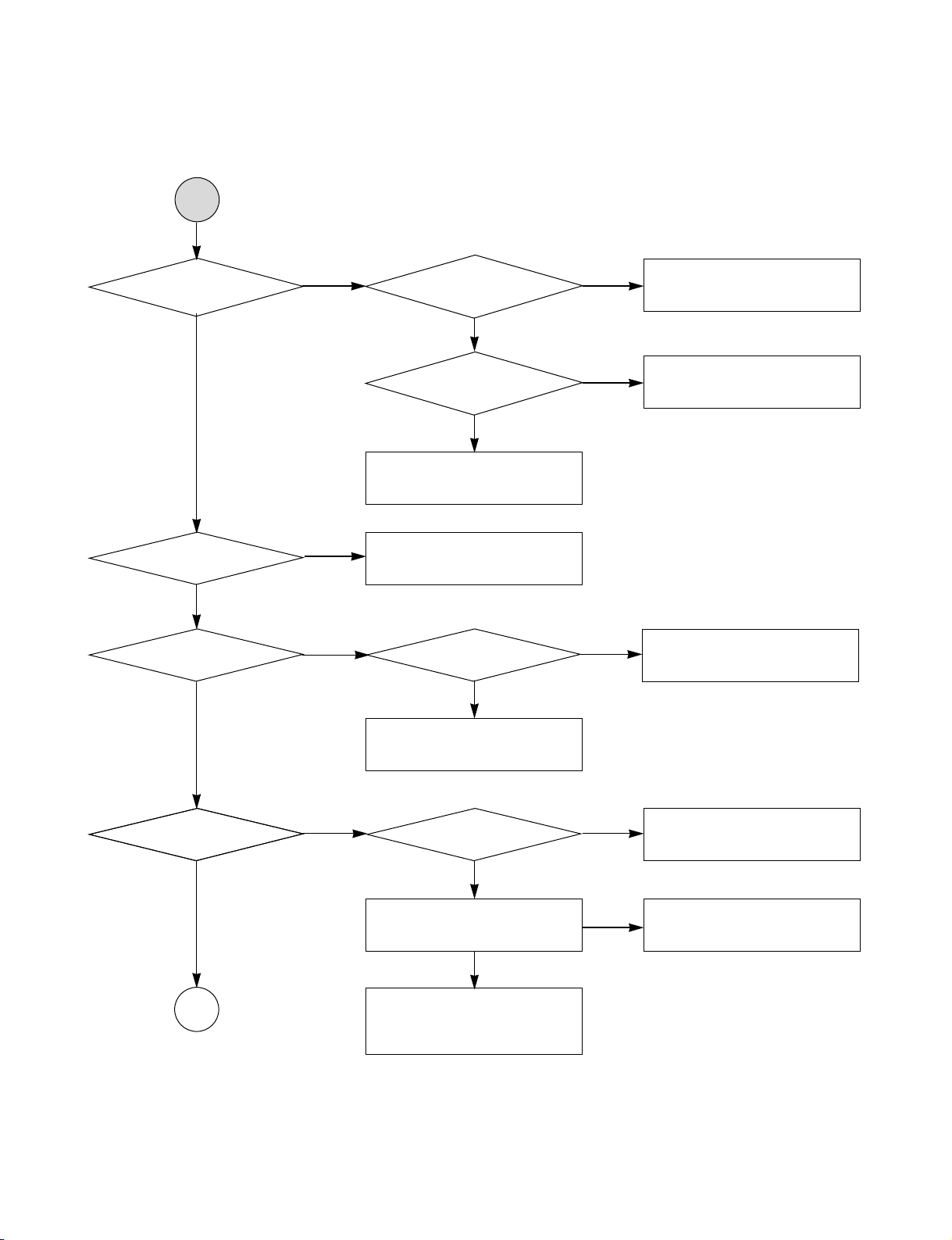
ELECTRICAL TROUBLESHOOTING GUIDE
D
Focus on OK?
YES
Track on OK?
NO NO
Proper signals on
A,B,C,D of ZR966
YES
Check focus_s
NO
signal on ZR966
YES
F+ & F- output
properly?
YES
Check cable connection on
pick-up head.
NO NO
Properly track_s
signal on ZR966?
YES
Check connections between
ZR966 and pick-up head.
Check the focus_s connection
on ZR966 and motor driver.
Check the focus control
amp circuit on motor driver.
Check the track_s connection
on ZR966 and motor dirver.
YES
Disc is play?
YES
E
NO
T+ & T- output
properly?
YES
Check cable connection on
pick-up head.
Check RF signal waveform.
3-8
NO
Check the tracking control
amp circuit on motor driver.
Page 20

ELECTRICAL TROUBLESHOOTING GUIDE
E
Normal
Audio output when disc
playback?
YES
Normal
IR.VFD & Front
pannel key
functions?
YES
NO
DAC received correct
Audio
NO
data stream?
YES
Normal Audio
NO
DAC out?
YES
Check Audio filter,
amplify, mute circuit.
Commu-
NO NO
nications between
IR.VFD Front pannel
key & ZR966 is
normally?
YES
Check connection between
ZR966 & Audio DAC.
Check the related
circuit of Audio DAC.
Check communication
lines on ZR966.
TEST END
Check the cable connection
on Front pannel.
3-9
Page 21

DETAILS AND WAVEFORMS ON SYSTEM TEST AND DEBUGGING
1. SYSTEM 27MHz CLOCK, RESET, FLASH R/W SIGNAL
1) ZR966 main clock is at 27MHz (X601)
1
1
2) ZR966 reset is active high.
2
3
4
FIG 1-1
3.3VA
2
3
PWR_CTL
RESET
4
FIG 1-2
3-10
Page 22

3) RS232 waveform during procedure (Downloading)
5
5
6
TXD
RXD
FIG 1-3
4) Flash R/W enable signal during download (Downloading)
7
7
PRD
6
IC602
8
PWR
8
FIG 1-4
3-11
Page 23

2. SDRAM CLOCK
DCLK = 128MHz, Vp-p=2.2, Vmax=2.7V
9
3. TRAY OPEN/CLOSE SIGNAL
IC603
9
FIG 2-1
10
11
12
13
11
INSW
OUTSW
10
IC201
CLOSE
13
OPEN
12
FIG 3-1
3-12
Page 24

4. SLED CONTROL RELATED SIGNAL (NO DISC CONDITION)
15
SLED_S(1.9V/1.4V/1.1V)
18
14
14
DRVSB(3.3V)
15
16
SLED+(4.2V/2.8V/1.2V)
16
17
SLED-(4.2V/2.8V/1.5V)
17
20
19
FIG 4-1
5. LENS CONTROL RELATED SIGNAL (NO DISC CONDITION)
18
19
20
FOCUS_S(1.5V/1.4V/1.3V)
FACT+(3.2V/2.7V/2.2V)
FACT-(3.2V/2.7V/2.2V)
FIG 5-1
3-13
Page 25

6. LASER POWER CONTROL RELATED SIGNAL (NO DISC CONDITION)
CN201
MDI1(0V/180mV)
21
21
22
23
CD_LD(3.3V//2.3V)
22
DVD_LD(3.3V/2.3V)
23
FIG 6-1
7. SPINDLE CONTROL WAVEFORM (NO DISC CONDITION)
SPINDLE_S(1.4V/1.8V)
24
25
SP-(3.6V/2.4V)
26
SP+(3.6V/4.8V)
FIG 7-1
3-14
24
25
26
Page 26

8. FOCUS ON WAVEFORM
27
28
29
27
FOCUS_S
FF+
FF-
IC201
27
FIG 8-1 (DVD)
28
FOCUS_S
29
28
29
FF+
FF-
FIG 8-2 (CD)
3-15
Page 27

9. RACKING CONTROL RELATED SIGNAL (SYSTEM CHECKING)
TRACK_S
30
30
31
32
30
Tracking+
Tracking-
FIG 9-1 (DVD)
TRACK_S
P2201
31
31
32
Tracking+
Tracking-
FIG 9-2 (CD)
3-16
32
Page 28

10. ZR966 AUDIO COAXIAL OUTPUT (SPDIF)
33
FIG 10-1
33
11. ZR966 VIDEO OUTPUT WAVEFORM
1) 100% COLOR BAR
FIG 11-1
3-17
Page 29

2) COMPOSITE VIDEO SIGNAL
FIG 11-2
12. AUDIO OUTPUT FROM ZR966
FIG 12-1
3-18
Page 30

CONNECTOR PICTURE
1. ALL CONNECTOR PICTURE
3-19
Page 31

2. P2201 CONNECTOR PICTURE
P2201 (MD 23PIN)
3. P2202 CONNECTOR PICTURE
P2202 (MD 9PIN)
3-20
Page 32

4. PW6101 CONNECTOR PICTURE
PW6101 (POWER 10PIN)
5. P6501 CONNECTOR PICTURE
P6501 (USB 4PIN) Not used currently
3-21
Page 33

6. P6602 CONNECTOR PICTURE
P6602 (DOWN LOAD 4PIN)
P6602 (HYPER TEAMINAL 4PIN)
7. P6901 CONNECTOR PICTURE
P6901 (TIMER 12PIN)
3-22
Page 34

8. P7301 CONNECTOR PICTURE
P7301 (SCART 12PIN)
3-23
Page 35

BLOCK DIAGRAMS
1. OVERALL BLOCK DIAGRAM
3-24
Page 36

2. POWER SUPPLY BLOCK DIAGRAM
3-25
Page 37

3. SERVO BLOCK DIAGRAM
3-26
Page 38

4. MPEG & MEMORY BLOCK DIAGRAM
3-27
Page 39

5. VIDEO BLOCK DIAGRAM
3-28
Page 40

6. AUDIO BLOCK DIAGRAM
3-29
Page 41

MEMO
3-30
Page 42

No Power
D105~D108 are Defective
12V No Power
Q123 is Defective
5V No Power
Q126 is Defective
Switching Error
IC102, IC103 are Defective
No Power
FR101 is Defective
Switching Error
IC101 is Defective
3.3V No Power
Q121 is Defective
CIRCUIT DIAGRAMS
1. POWER (SMPS) CIRCUIT DIAGRAM
IMPORTANT SAFETY NOTE :
WHEN SERVICING THIS CHASSIS, UNDER NO
CIRCUMSTANCES SHOULD THE ORIGINAL DESIGN
BE MODIFIED OR ALTERED WITHOUT PERMISSION
FROM THE JVC. ALL COMPONENTS SHOULD BE
REPLACED ONLY WITH TYPES IDENTICAL TO
THOSE IN THE ORIGINAL CIRCUIT. SPECIAL
COMPONENTS ARE SHADED ON THE SCHEMATIC
FOR EASY IDENTIFICATION. THIS CIRCUIT DIAGRAM
MAY OCCASIONALLY DIFFER FROM THE ACTUAL
CIRCUIT USED. THIS WAY, IMPLEMENTATION OF THE
LATEST SAFETY AND PERFORMANCE
IMPROVEMENT CHANGES INTO THE SET IS NOT
DELAYED UNTIL THE NEW SERVICE LITERATURE IS
PRINTED.
1. Shaded( ) parts are critical for safety. Replace only
with specified part number.
2. Voltages are DC-measured with a digital voltmeter
during Play mode.
3-31 3-32
Page 43

2. SYSTEM (MPEG) CIRCUIT DIAGRAM
3-33 3-34
Page 44

3. SERVO CIRCUIT DIAGRAM
3-35 3-36
Page 45

4. AV/JACK CIRCUIT DIAGRAM
3-37 3-38
Page 46

5. TIMER/KEY CIRCUIT DIAGRAM
3-39 3-40
Page 47

• CIRCUIT VOLTAGE CHART
PIN No Disc Play
IC201
1 1.33 1.66
2 1.84 1.83
3 2.76 3
4 1.28 1.65
5 1.25 1.24
6 3.28 3.24
7 0.0003 0.0003
8 4.89 4.97
9 0.53 0.435
10 3.83 3.99
11 2.29 2.47
12 2.29 2.45
13 2.34 2.27
14 2.34 2.54
15 2.32 2.4
16 2.32 2.41
17 1.34 3.32
18 1.34 1.49
19 4.87 4.97
20 0.92 1.03
21 4.87 4.99
22 0.0007 0.001
23 1.01 1.94
24 0.435 0.4
25 4.81 4.93
26 1.35 1.64
27 1.65 1.64
28 0.004 3.17
IC601
1 1.91 1.97
2 1.56 2.109
3 1.32 2.117
4 2.61 2.328
5 0.64 1.51
6 1.32 1.46
7 1.51 1.61
8 1.64 1.08
9 0.97 2.31
10 0.72 1.49
11 0.0002 0.0003
12 1.71 1.13
13 1.77 1.966
14 1.756 0.278
15 3.28 0.281
16 0.23 0.36
17 3.28 0.297
18 3.23 0.293
19 3.21 0.279
20 0.03 1.09
21 2.45 2.21
22 0.78 1.04
23 1.45 1.75
24 1.18 1.68
25 1.6 1.72
26 3.28 3.25
27 0.001 0.36
28 1.61 2.35
29 1.13 1.03
PIN No Disc Play
30 3.28 1.51
31 0.0001 0.001
32 1.83 2.15
33 0.31 1.83
34 0.72 0.32
35 3.28 0.35
36 0.87 0.62
37 2.56 0.24
38 0.002 0.31
39 3.28 0.3
40 0.003 0.31
41 0.004 0.31
42 0.003 0.003
43 1.67 0.24
44 1.86 0.25
45 1.69 0.28
46 3.28 3.25
47 0.0001 0.0001
48 0.92 1.31
49 1.63 1.57
50 1.57 1.68
51 1.62 1.57
52 1.75 1.74
53 1.58 1.21
54 0.015 0.015
55 0.003 0.007
56 3.28 3.28
57 0.0001 0.0001
58 0.004 3.28
59 0.004 0.005
60 3.24 3.21
61 0.035 0.035
62 3.2 3.16
63 3.2 3.23
64 3.26 3.18
65 3.28 3.28
66 0.0001 0.0001
67 3.22 3.24
68 2.9 2.83
69 0.0001 0.0004
70 3.25 0.26
71 3.29 3.24
72 1.51 0.07
73 0.04 1.24
74 1.87 1.67
75 2.68 1.54
76 3.28 3.249
77 0.0001 0.0001
78 1.56 1.22
79 1.87 1.64
80 1.51 1.61
81 1.69 2.13
82 1.78 0.07
83 1.49 1.52
84 3.32 3.247
85 0.001 0.001
86 0.67 0.98
87 1.86 1.13
88 3.32 1.742
PIN No Disc Play
89 1.61 0.93
90 1.59 1.91
91 1.15 1.87
92 1.42 1.93
93 3.32 3.249
94 0.002 3.24
95 0.0005 0.0005
96 0.45 0.51
97 0.002 0.003
98 0 0.0001
99 0 0.0001
100 0.0001 0.001
101 3.28 3.24
102 0.0005 0.001
103 0.001 0.001
104 3.26 3.21
105 3.281 3.246
106 0.001 0.0008
107 0.0005 0.0009
108 0.0008 0.0008
109 0.0006 0.0006
110 0.0001 0.0002
111 0.0005 0.0006
112 0.0005 0.0006
113 1.642 1.62
114 1.642 1.62
115 1.642 1.62
116 1.642 1.62
117 0.0005 0.0005
118 0.0001 0.0009
119 0.0008 0.0007
120 0.005 0.005
121 3.286 3.247
122 1.635 1.617
123 0.005 0.005
124 0.047 0.053
125 0.005 0.005
126 0.005 0.005
127 0.005 0.005
128 3.27 3.22
129 4.31 4.18
130 3.82 3.72
131 0.013 0.015
132 0.005 0.005
133 3.62 3.32
134 3.295 3.72
135 3.286 3.252
136 3.284 3.22
137 3.281 3.25
138 3.284 3.25
139 3.281 3.25
140 1.75 1.747
141 0.0003 0.0003
142 3.286 3.248
143 0.0003 0.0005
144 1.751 1.745
145 1.59 1.57
146 1.63 1.61
147 1.35 1.57
PIN No Disc Play
148 0.0002 0.0005
149 0.0003 0.0005
150 3.279 3.24
151 0.93 1.166
152 0.0001 0.0003
153 3.278 3.242
154 0.0002 0.0003
155 1.233 1.235
156 0.0002 0.0003
157 0.0003 1.67
158 0.0003 1.67
159 3.29 3.23
160 0.69 2.26
161 0.21 2.24
162 3.29 3.24
163 0.22 2.254
164 0.68 2.257
165 1.75 1.75
166 0.81 2.37
167 0.436 0.397
168 0.812 2.36
169 0.0001 0.003
170 0.256 1.726
171 1.598 1.694
172 0.0001 0.003
173 0.806 2.097
174 0.001 1.647
175 0.002 0.93
176 0.0001 0.003
177 3.29 3.24
178 0.0001 0.199
179 0.0001 0.006
180 3.29 2.36
181 3.29 3.22
182 0.0001 1.733
183 3.29 3.25
184 0.0015 1.612
185 0.0001 0.0002
186 0.0029 2.484
187 0.0018 1.697
188 3.28 3.24
189 0.0003 0.0005
190 1.754 1.749
191 0.0002 0.0003
192 0.003 0.003
193 3.37 3.37
194 0.0003 0.0003
195 3.27 0.0003
196 0.029 0.067
197 3.19 3.21
198 3.09 3.08
199 0.003 0.003
200 3.29 3.262
201 1.88 2.49
202 3.22 2.87
203 3.23 2.81
204 1.52 2.65
205 1.65 2.6
206 1.68 2.75
PIN No Disc Play
207 1.61 2.47
208 3.28 3.25
IC603
1 3.31 3.3
2 1.42 1.93
3 3.31 3.3
4 1.59 1.91
5 1.86 1.13
6 0.0002 0.0003
7 1.49 1.52
8 1.69 2.13
9 3.31 3.3
10 1.87 1.64
11 2.68 1.54
12 0.0001 0.0002
13 0.04 1.24
14 3.31 3.3
15 2.9 2.83
16 3.22 3.24
17 3.26 3.18
18 3.2 3.23
19 3.2 3.16
20 0.035 0.035
21 3.24 3.21
22 0.003 0.008
23 1.5 1.28
24 1.51 1.71
25 0.95 1.31
26 1.87 1.6
27 3.31 3.3
28 0.0002 0.0003
29 1.66 1.6
30 1.7 1.61
31 1.6 1.58
32 1.62 1.58
33 0.016 0.013
34 0.004 0.021
35 0.003 0.004
36 0.0002 0.005
37 0.45 0.51
28 0.227 0.24
39 2.9 2.82
40 0.004 0.004
41 0.0001 0.005
42 1.51 0.07
43 3.31 3.29
44 1.87 1.67
45 1.56 1.22
46 0.0002 0.0001
47 1.51 1.61
48 1.78 0.07
49 3.31 3.29
50 0.67 0.98
51 1.61 0.93
52 0.0002 0.0003
53 1.15 1.87
54 0.0002 0.0003
IC604
1 3.21 2.56
PIN No Disc Play
2 3.22 2.16
3 0.16 0.97
4 2.48 2.31
5 0.85 1.05
6 1.8 1.71
7 1.25 1.75
8 1.32 1.65
9 0.001 0.002
10 3.28 3.28
11 3.28 3.28
12 3.31 3.29
13 3.31 3.29
14 3.31 3.29
15 1.76 1.71
16 0.001 0.31
17 1.88 2.49
18 1.32 1.13
19 1.8 1.53
20 1.8 1.68
21 0.28 1.78
22 0.8 1.59
23 0.95 1.56
24 2.75 2.93
25 3.19 2.93
26 3.23 2.79
27 0.002 0.0005
28 3.23 2.81
29 1.52 2.65
30 1.65 2.6
31 1.68 2.75
32 1.61 2.47
33 1.68 2.59
34 1.55 2.57
35 1.65 2.67
36 2.79 2.69
37 3.3 3.29
38 0.53 1.91
39 1.37 2.03
40 1.37 2.31
41 1.76 0.81
42 0.91 2.21
43 0.76 2.4
44 1.71 1.95
45 1.91 1.59
46 0.017 0.005
47 3.3 3.29
48 0.15 0.51
IC702
1 7.21 7.32
2 4.3 4.34
3 4.29 4.32
4 0.002 0.004
5 4.28 4.31
6 4.29 4.32
7 7.24 7.32
811.84 11.98
DC VOLTMETER MEASUREMENT METHOD
condenser Capacitor Compressive(V)
C617 100uF 16V 3.25 0.00
C623 100uF 16V 1.75 0.00
C624 100uF 16V 3.25 0.00
C627 220uF 6.3V 3.242 0.00
C640 100uF 16V NC NC
C644 47uF 6.3V 3.25 0.00
C646 47uF 6.3V 1.76 0.00
C649 47uF 6.3V 3.30 0.00
C661 10uF 16V 3.25 0.00
C678 33uF 16V 2.42 0.00
C155 220uF 16 12.01 3.99V
C156 330uF 10 4.98 5.02V
C6C9 220uF 6.3V 3.29 0.00
C201 100uF 16V 4.94 0.00
C208 47uF 6.3V 3.29 3.23
C209 47uF 6.3V 3.29 2.41
C214 470uF 6.3V 4.94 0.00
C221 47uF 16V NC NC
C223 47uF 6.3V 3.29 0.00
C716 22uF 16V 6.63 0.00
C717 22uF 16V 6.66 0.00
C727 22uF 16V 0.37 0.00
C728 470uF 16V 11.98 0.00
C729 220uF 16V NC NC
C741 47uF 6.3V NC NC
C787 47uF 6.3V 0.17 0.00
TR
Q201 3.29 0.05 3.23
Q202 3.11 2.04 2.41
Q203 2.50 1.78 1.85
Q701 0.00 0.00 2.41
Q702 0.00 0.00 3.25
Q703 3.24 -2.73 3.31
Q711 0.00 0.00 0.07
Q712 0.00 0.00 0.07
Q713 0.00 0.00 0.07
Q714 3.02 4.96 0.07
E/S C/D B/G
PLAY
Playback
+/A -/K
3-41 3-42
Page 48

PRINTED CIRCUIT BOARD DIAGRAMS
1. MAIN P.C.BOARD
(TOP VIEW) (BOTTOM VIEW)
3-43 3-44
Page 49

2. KEY P.C.BOARD
(TOP VIEW) (BOTTOM VIEW)
3. TIMER P.C.BOARD
(TOP VIEW)
(BOTTOM VIEW)
3-45 3-46
Page 50

4. SMPS P.C.BOARD
5. SCART P.C.BOARD (SCART MODEL ONLY)
(TOP VIEW) (BOTTOM VIEW)
3-47 3-48
Page 51

MEMO MEMO
3-49 3-50
Page 52

4-1
SECTION 4
MECHANISM (DP-11)
CONTENTS
DECK MECHANISM PARTS LOCATIONS
• TOP VIEW....................................................................................................................................4-2
• TOP VIEW (WITHOUT TRAY DISC) ...........................................................................................4-2
• BOTTOM VIEW ...........................................................................................................................4-2
DECK MECHANISM DISASSEMBLY
1. MAIN BASE ...............................................................................................................................4-3
1-1. Clamp Assembly Disc .........................................................................................................4-3
1-1-1. Plate Clamp ..............................................................................................................4-3
1-1-2. Magnet Clamp ..........................................................................................................4-3
1-1-3. Clamp Upper ............................................................................................................4-3
2. TRAY DISC ................................................................................................................................4-3
3. BASE ASSEMBLY SLED ..........................................................................................................4-4
3-1. Gear Feed...........................................................................................................................4-4
3-2. Gear Middle ........................................................................................................................4-4
3-3. Gear Rack...........................................................................................................................4-4
4. RUBBER REAR.........................................................................................................................4-4
5. FRAME ASSEMBLY UP/DOWN................................................................................................4-5
6. BELT LOADING.........................................................................................................................4-5
7. GEAR PULLEY..........................................................................................................................4-5
8. GEAR LOADING .......................................................................................................................4-5
9. GUIDE UP/DOWN .....................................................................................................................4-5
10. PWB ASSEMBLY LOADING...................................................................................................4-5
11. BASE MAIN .............................................................................................................................4-5
EXPLODED VIEW
1. DECK MECHANISM EXPLODED VIEW...................................................................................4-7
Page 53

4-2
DECK MECHANISM PARTS LOCATION
• TOP VIEW (WITHOUT TRAY)
Procedure
Parts Fixing Type
Disass Fig-
Starting No.
embly ure
1 Main Base 4-1
12
Clamp Assembly
4-1
Disc
1, 2 3 Plate Clamp 4-1
1, 2, 3 4 Magnet Clamp 4-1
1, 2, 3, 4 5 Clamp Upper 4-1
16Tray Disc 4-2
1, 6 7 Base Assembly Sled 4-3
4 Screws,
1, 2, 6 8 Gear Feed 1 Connector 4-3
1 Locking Tabs
1, 2, 6, 8 9 Gear Middle
1, 2, 6, 8,
10 Gear Rack 1 Screw 4-3
9
1, 2, 7 11 Rubber Rear 4-3
1, 2, 7 12
Frame Assembly
1 Screw Bottom 4-4
Up/Down
1, 2 13 Belt Loading 1 Locking Tab 4-4
1, 2 ,13 14 Gear Pulley 4-4
1, 2, 13, 14 15 Gear Loading 1 Locking Tab 4-4
1, 2, 7, 12,
16 Guide Up/Down 4-4
13, 14
1, 2, 13 17 PWB Assembly
1 Locking Tab
Bottom 4-4
Loading
1 Hook
2Screw
1, 2, 7, 12,
13, 14, 15, 18 Base Main 2 Locking Tabs 4-4
16, 17
• TOP VIEW (WITH TRAY)
• BOTTOM VIEW
Note
When reassembling, perform the procedure in
reverse order.
The “Bottom” on Disassembly column of above
Table indicates the part should be disassembled
at the Bottom side.
Page 54

4-3
1. MAIN BASE (FIG. 4-1)
1-1. Clamp Assembly Disc
1) Place the Clamp Assembly Disc as Fig. (A)
2) Lift up the Clamp Assembly Disc in direction of
arrow(A).
3) Separate the Clamp Assembly Disc from the
Holder Clamp.
1-1-1. Plate Clamp
1) Turn the Plate Clamp to counterclockwise
direction and then lift up the Plate Clamp.
1-1-2. Magnet Clamp
1-1-3. Clamp Upper
2. TRAY DISC (FIG. 4-2)
1) Insert and push a Driver in the emergency eject
hole(A) at the right side, or put the Driver on the
Lever(B) of the Gear Emergency and pull the
Lever(B) in direction of arrow so that the Tray
Disc is ejected about 15~20mm.
2) Pull the Tray Disc until it is separated from the
Base Main completely.
DECK MECHANISM DISASSEMBLY
FIG. 4-1 FIG. 4-2
Page 55

4-4
3. BASE ASSEMBLY SLED (FIG. 4-3)
1) Release 4 Screw (S2).
2) Disconnect the FFC Connector (C1)
3-1. Gear Feed
3-2. Gear Middle
3-3. Gear Rack
1) Release the Scerw (S3)
4. RUBBER REAR (FIG. 4-3)
FIG. 4-3
Page 56

4-5
5. FRAME ASSEMBLY UP/DOWN (FIG. 4-4)
Note
Put the Base Main face down (Bottom Side)
1) Release the screw (S4)
2) Unlock the Locking Tab (L3) in direction of arrow
and then lift up the Frame Assembly Up/Down to
separate it from the Base Main.
Note
• When reassembling move the Guide Up/Down in
direction of arrow(C) until it is positioned as
Fig.(C).
• When reassembling insert (A) portion of the
Frame Assembly Up/Down in the (B) portion of
the Guide Up/Down as Fig.(B)
6. BELT LOADING(FIG. 4-4)
Note
Put the Base Main on original position(Top Side)
7. GEAR PULLEY (FIG. 4-4)
1) Unlock the Locking Tab(L4) in direction of
arrow(B) and then separate the Gear Pulley from
the Base Main
8. GEAR LOADING (FIG. 4-4)
9. GUIDE UP/DOWN (FIG. 4-4)
1) Move the Guide Up/Down in direction of
arrow(A) as Fig.(A)
2) Push the Locking Tab(L5) down and then lift up
the Guide Up/Down to separate it from the Base
Main.
Note
When reassembling place the Guide Up/Down as
Fig.(C) and move it in direction arrow(B) until it is
locked by the Locking Tab(L5). And confirm the Guide
Up/Down as Fig.(A)
10. PWB ASSEMBLY LOADING (FIG. 4-4)
Note
Put the Base Main face down(Bottom Side)
1) Release 1 Screws(S5)
2) Unlock the Loading Motor (C2) from the Hook
(H1) on the Base Main.
3) Unlock 2 Locking Tabs(L6) and separate the
PWB Assembly Loading from the Base Main.
11. BASE MAIN (FIG. 4-4)
FIG. 4-4
Page 57

4-6
MEMO
Page 58

001
002
003
020
439
018
013
017
015B
015A
440
019
012
015
012
432
030
010
439
431
435
021
430
024
025
036
012A
012A
026
016
435
014
A01
A02
A03
A00
4-7 4-8
EXPLODED VIEW
1. DECK MECHANISM EXPLODED VIEW
DP-11
Page 59

4-9 4-10
MEMO MEMO
 Loading...