

Page 1
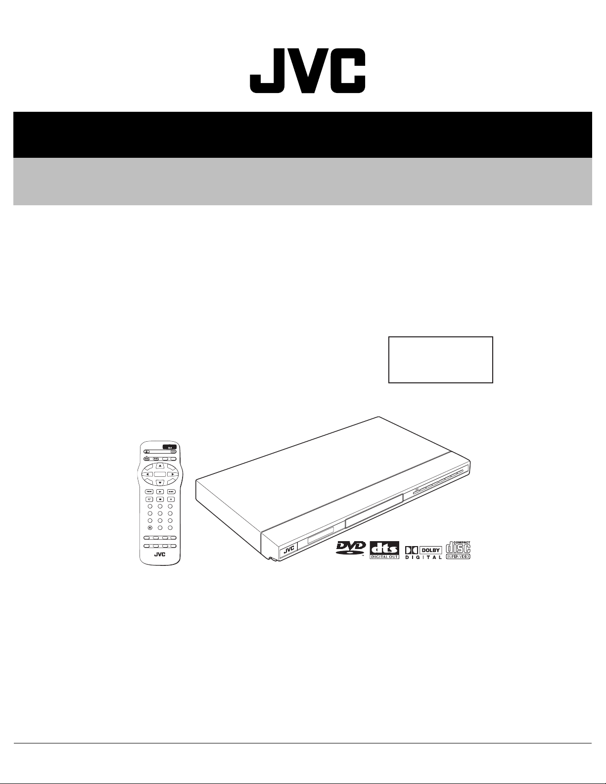
SERVICE MANUAL
DVD PLAYER
YD09520064
XV-N330BUS,XV-N330BUC,
XV-N330BUJ,XV-N332SUS,
XV-N332SUC,XV-N332SUJ
Area Suffix
US ----------------------- U.S.A.
UC ------------------- Canada
UJ ------------ U.S.A Militaly
STANDBY/ON
OPEN/
CLOSE
+
SLOW
DISPLAYON SCREEN
T
O
T
P
H
U
M
B
N
A
IL
L
ENTER
S
NEXTPREVIOUS
SELECT
CLEAR
123
456
789
0
SOUND
VFP
EFFECT
I/P
SUBTITLEANGLE
AUDIO
ZOOM
/
IS
T
E
T
U
P
®
VIDEO
M
E
N
U
M
E
N
U
CANCEL RETURN
TITLE/
GROUP DIMMER
SLIDE EFFECT
XV-N330BUSC,XV-N330BUCC,XV-N330BUJC,XV-N332SUSC,XV-N332SUCC,XV-N332SUJC [D6P1]
TABLE OF CONTENTS
1 PRECAUTION. . . . . . . . . . . . . . . . . . . . . . . . . . . . . . . . . . . . . . . . . . . . . . . . . . . . . . . . . . . . . . . . . . . . . . . . . 1-3
2 SPECIFIC SERVICE INSTRUCTIONS . . . . . . . . . . . . . . . . . . . . . . . . . . . . . . . . . . . . . . . . . . . . . . . . . . . . . . 1-8
3 DISASSEMBLY . . . . . . . . . . . . . . . . . . . . . . . . . . . . . . . . . . . . . . . . . . . . . . . . . . . . . . . . . . . . . . . . . . . . . . . 1-9
4 ADJUSTMENT . . . . . . . . . . . . . . . . . . . . . . . . . . . . . . . . . . . . . . . . . . . . . . . . . . . . . . . . . . . . . . . . . . . . . . . 1-16
5 TROUBLESHOOTING . . . . . . . . . . . . . . . . . . . . . . . . . . . . . . . . . . . . . . . . . . . . . . . . . . . . . . . . . . . . . . . . . 1-19
COPYRIGHT © 2006 Victor Company of Japan, Limited
No.YD095
2006/4
Page 2
SPECIFICATION
XV-N330BUS,XV-N330BUC,XV-N332SUS,XV-N332SUC
General
Readable discs DVD VIDEO, DVD-R/-RW (Video format), +R/+RW(Video format), SVCD, Video CD, Audio CD (CD-
DA), CD-R/RW (CD-DA, SVCD, Video CD, MP3 format, JPEG)
Video format NTSC, 480i/480p selectable
Other
Power requirements AC 120 V~, 60 Hz AC 110 V - 240 V~, 50 Hz/60 Hz
Power consumption 11.0 W (POWER ON), 1.0 W (STANDBY mode)
Mass 1.5 kg (3.3 lbs)
Dimensions (W × H × D) 435mm × 44mm × 201.5 mm (17-3/16 inch × 1-3/4 inc × 7-15/16 inch)
Video outputs
COMPONENT (pin jacks) Y Output: 1.0 Vp-p (75 Ω)
Pb/Pr Output: 0.7Vp-p (75 Ω)
VIDEO (pin jack) 1.0 Vp-p (75 Ω)
S-VIDEO (S jack) Y Output: 1.0 Vp-p (75 Ω)
C Output: 286 mVp-p (75 Ω)
Horizontal resolution 500 lines or more
Audio outputs
ANALOG OUT (pin jack) 2.0 Vrms (10 kΩ)
DIGITAL OUT (COAXIAL) 0.5 Vp-p (75 Ω termination)
Audio characteristics
Frequency response CD (sampling frequency 44.1 kHz):2 Hz to 20 kHz
DVD (sampling frequency 48 kHz):2 Hz to 22 kHz
(4 Hz to 20 kHz for DTS and Dolby Digital bitstream signals)
DVD (sampling frequency 96 kHz):2 Hz to 44 kHz
Wow and flutter Unmeasurable (less than +- 0.002%)
XV-N330BUJ,XV-N332SUJ
• Manufactured under license from Dolby Laboratories. “Dolby” and the double-D symbol are trademarks of Dolby Laboratories.
• “DTS” and “DTS Digital Out” are trademarks of Digital Theater Systems, Inc.
• This product incorporates copyright protection technology that is protected by U.S. patents and other intellectual property rights. Use
of this copyright protection technology must be authorized by Macrovision, and is intended for home and other limited viewing uses
only unless otherwise authorized by Macrovision. Reverse engineering or disassembly is prohibited.
1-2 (No.YD095)
Page 3
SECTION 1
PRECAUTION
1.1 Safety Precautions
(1) This design of this product contains special hardware and
many circuits and components specially for safety purposes. For continued protection, no changes should be made
to the original design unless authorized in writing by the
manufacturer. Replacement parts must be identical to
those used in the original circuits. Services should be performed by qualified personnel only.
(2) Alterations of the design or circuitry of the product should
not be made. Any design alterations of the product should
not be made. Any design alterations or additions will void
the manufacturers warranty and will further relieve the
manufacture of responsibility for personal injury or property
damage resulting therefrom.
(3) Many electrical and mechanical parts in the products have
special safety-related characteristics. These characteristics are often not evident from visual inspection nor can the
protection afforded by them necessarily be obtained by using replacement components rated for higher voltage, wattage, etc. Replacement parts which have these special
safety characteristics are identified in the Parts List of Service Manual. Electrical components having such features
are identified by shading on the schematics and by ( ) on
the Parts List in the Service Manual. The use of a substitute
replacement which does not have the same safety characteristics as the recommended replacement parts shown in
the Parts List of Service Manual may create shock, fire, or
other hazards.
(4) The leads in the products are routed and dressed with ties,
clamps, tubings, barriers and the like to be separated from
live parts, high temperature parts, moving parts and/or
sharp edges for the prevention of electric shock and fire
hazard. When service is required, the original lead routing
and dress should be observed, and it should be confirmed
that they have been returned to normal, after reassembling.
(5) Leakage shock hazard testing)
After reassembling the product, always perform an isolation check on the exposed metal parts of the product (antenna terminals, knobs, metal cabinet, screw heads,
headphone jack, control shafts, etc.) to be sure the product
is safe to operate without danger of electrical shock.Do not
use a line isolation transformer during this check.
• Plug the AC line cord directly into the AC outlet. Using a
"Leakage Current Tester", measure the leakage current
from each exposed metal parts of the cabinet, particularly any exposed metal part having a return path to the
chassis, to a known good earth ground. Any leakage current must not exceed 0.5mA AC (r.m.s.).
• Alternate check method
Plug the AC line cord directly into the AC outlet. Use an
AC voltmeter having, 1,000 ohms per volt or more sensitivity in the following manner. Connect a 1,500 ohm 10W
resistor paralleled by a 0.15 F AC-type capacitor between an exposed metal part and a known good earth
ground.
Measure the AC voltage across the resistor with the AC
voltmeter.
Move the resistor connection to each exposed metal
part, particularly any exposed metal part having a return
path to the chassis, and measure the AC voltage across
the resistor. Now, reverse the plug in the AC outlet and
repeat each measurement. Voltage measured any must
not exceed 0.75 V AC (r.m.s.). This corresponds to 0.5
mA AC (r.m.s.).
AC VOLTMETER
(Having 1000
ohms/volts,
or more sensitivity)
0.15 F AC TYPE
Place this
probe on
1500 10W
Good earth ground
1.2 Warning
(1) This equipment has been designed and manufactured to
meet international safety standards.
(2) It is the legal responsibility of the repairer to ensure that
these safety standards are maintained.
(3) Repairs must be made in accordance with the relevant
safety standards.
(4) It is essential that safety critical components are replaced
by approved parts.
(5) If mains voltage selector is provided, check setting for local
voltage.
1.3 Caution
Burrs formed during molding may be left over on some parts
of the chassis.
Therefore, pay attention to such burrs in the case of preforming repair of this system.
1.4 Critical parts for safety
In regard with component parts appearing on the silk-screen
printed side (parts side) of the PWB diagrams, the parts that are
printed over with black such as the resistor ( ), diode ( )
and ICP ( ) or identified by the " " mark nearby are critical for
safety. When replacing them, be sure to use the parts of the
same type and rating as specified by the manufacturer. (Except
the JC version)
each exposed
metal part.
(No.YD095)1-3
Page 4
1.5 Preventing static electricity
Electrostatic discharge (ESD), which occurs when static electricity stored in the body, fabric, etc. is discharged, can destroy the laser
diode in the traverse unit (optical pickup). Take care to prevent this when performing repairs.
1.5.1 Grounding to prevent damage by static electricity
Static electricity in the work area can destroy the optical pickup (laser diode) in devices such as DVD players.
Be careful to use proper grounding in the area where repairs are being performed.
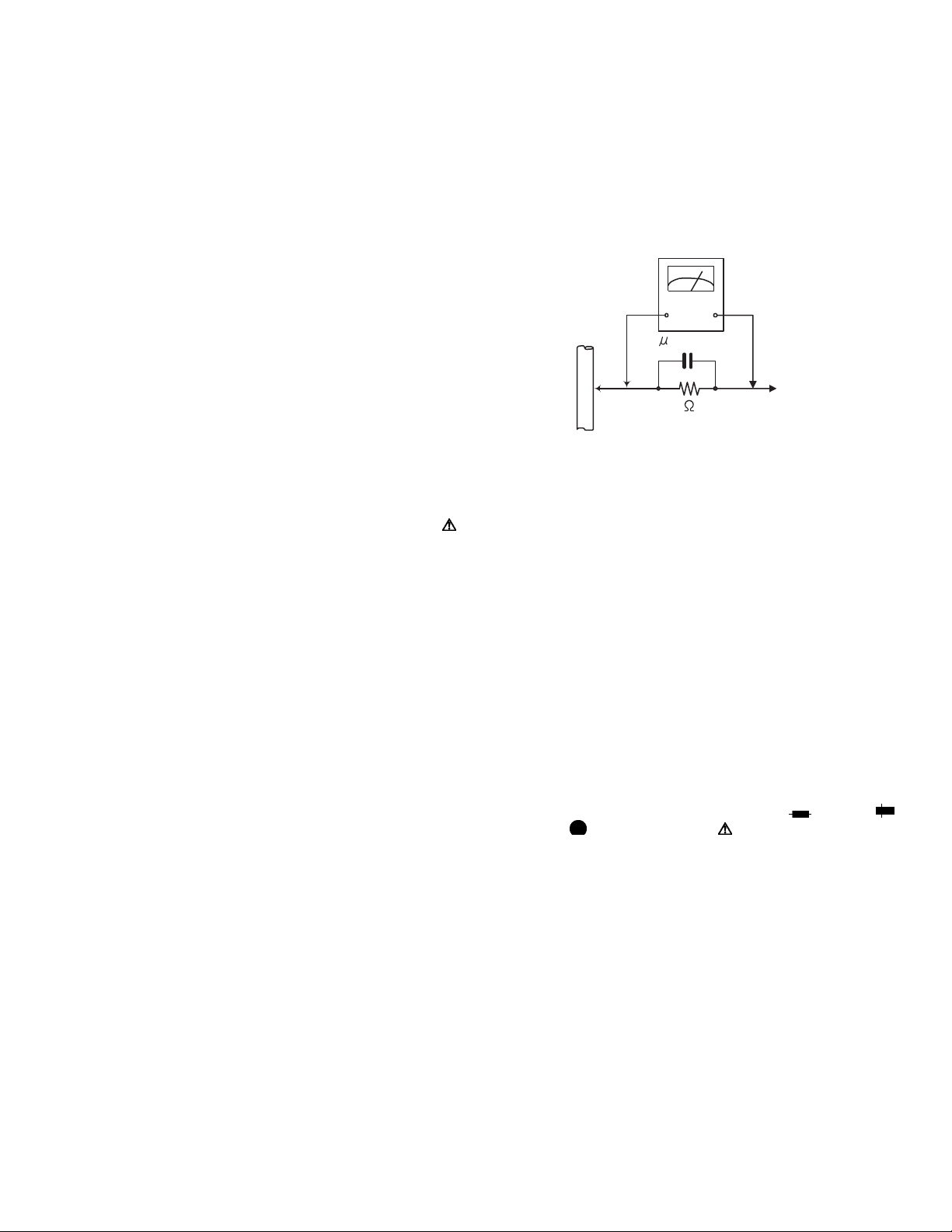
(1) Ground the workbench
Ground the workbench by laying conductive material (such as a conductive sheet) or an iron plate over it before placing the
traverse unit (optical pickup) on it.
(2) Ground yourself
Use an anti-static wrist strap to release any static electricity built up in your body.
(caption)
Anti-static wrist strap
1M
Conductive material
(conductive sheet) or iron palate
(3) Handling the optical pickup
• In order to maintain quality during transport and before installation, both sides of the laser diode on the replacement optical
pickup are shorted. After replacement, return the shorted parts to their original condition.
(Refer to the text.)
• Do not use a tester to check the condition of the laser diode in the optical pickup. The tester's internal power source can easily
destroy the laser diode.
1.6 Handling the traverse unit (optical pickup)
(1) Do not subject the traverse unit (optical pickup) to strong shocks, as it is a sensitive, complex unit.
(2) Cut off the shorted part of the flexible cable using nippers, etc. after replacing the optical pickup. For specific details, refer to the
replacement procedure in the text. Remove the anti-static pin when replacing the traverse unit. Be careful not to take too long
a time when attaching it to the connector.
(3) Handle the flexible cable carefully as it may break when subjected to strong force.
(4) I t is not possible to adjust the semi-fixed resistor that adjusts the laser power. Do not turn it.
1.7 Precautions of the safe use of battery
• Store the battery in a place where children cannot reach.If a child accidentally swallows the battery, consult a doctorimmediately.
• Do not recharge, short, disassemble or heat the battery or dispose of it in a fire.
Doing any of these things may cause the battery to give off heat, crack, or start a fire.
• Do not leave the battery with other metallic materials.Doing this may cause the battery to give off heat, crack, or start a fire.
• When throwing away or saving the battery, wrap it in tape and insulate; otherwise, the battery may start to give off heat, crack, or
start a fire.
• Do not poke the battery with tweezers or similar tools.Doing this may cause the battery to give off heat, crack, or start a fire.
• Dispose of batteries in the proper manner, according to federal, state, and local regulations.
1-4 (No.YD095)
Page 5
1.8 Importance administering point on the safety
CN903
B918
B902
S501S502
B916
B915
S507
B910
S506
R963
Q951
S508
L955
S503 S504
C957
CP951
S505
D960
C950
CN902
B912
B908
B907
C985
B950
C966
C964
L953
L954
C955
D954
C956
CP952
C982
CP950
B701
B913
EP902
B905
B904
L952
B901
C959
C954
D953
C983
D955
D956
B903
D957
D952
D951
L960
B716
B731
B730
B712
B714
B704
B703
B702
CN901
B906
C958
C902
L951
B713
C726
B706
B705
B708
B740
B919
B742
B743
L970
IC902
C905
PC901
R902
D906
C909
IC901
C908
D905
D902
R901
C906
T901
B715
B717
B722
C755
B711
B709
B760
CN905
B762
B745
B746
B744
L702
B917
C907
B718
C756
B729
B728
C728
B727
L709
L730
B761
L706
L701
B747
B748
B749
C903
C904
D903
L901
B723
B721
EP901
B720
B719
B765
B764
B759
B763
B758
B757
B754
C730
B751
B752
B750
C901
P901
FC901
J901
C706
C707
B726
C712
C713
B770
B767
B769
B768
B766
J601
CN904
B771
B756
L707
J703
J602
B753
B755
FC902
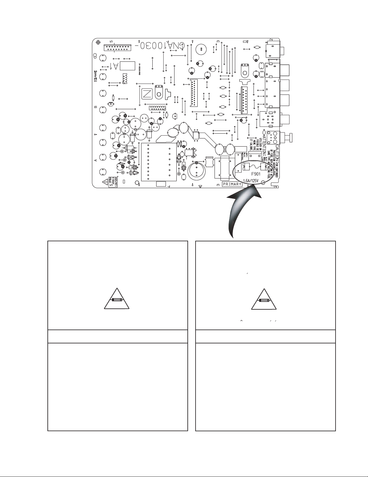
Full Fuse Replacement Marking
Graphic symbol mark
(This symbol means fast blow type fuse.)
should be read as follows ;
FUSE CAUTION
FOR CONTINUED PROTECTION AGAINST RISK
OF FIRE, REPLACE ONLY WITH SAME TYPE
AND RATING OF FUSES ;
F901 : 1.6 A / 125 V F901 : 1.6 A / 125 V
Marquage Pour Le Remplacement
Complet De Fusible
Le symbole graphique (Ce symbole signifie
fusible de type a fusion rapide.)
doit etre interprete comme suit ;
PRECAUTIONS SUR LES FUSIBLES
POUR UNE PROTECTION CONTINUE CONTRE
DES RISQUES D'INCENDIE, REMPLACER
SEULEMENT PAR UN FUSIBLE DU MEME TYPE ;
(No.YD095)1-5
Page 6
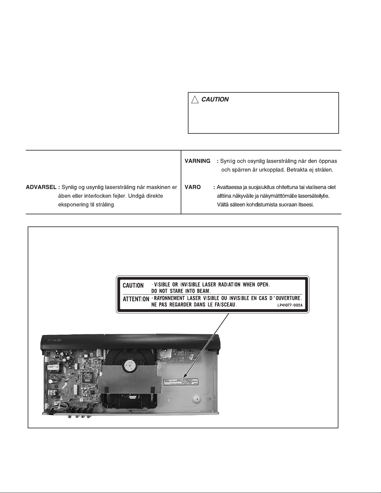
1.9 Important for laser products
!
1.CLASS 1 LASER PRODUCT
2.CAUTION : VISIBLE OR INVISIBLE LASER RADIATION
WHEN OPEN.
DO NOT STARE INTO BEAM.
3.CAUTION : There are no serviceable parts inside the
Laser Unit. Do not disassemble the Laser Unit. Replace
the complete Laser Unit if it malfunctions.
4.CAUTION : The laser products uses visible and / or
invisible laser radiation and is equipped with safety
switches which prevent emission of radiation when the
drawer is open and the safety interlocks have failed or are
defeated. It is dangerous to defeat the safety switches.
CAUTION : VISIBLE OR INVISIBLE LASER RADIATION
WHEN OPEN.
DO NOT STARE INTO BEAM.
5.CAUTION : If safety switches malfunction, the laser is able
to function.
6.CAUTION : Use of controls, adjustments or performance of
procedures other than those specified here in may result in
hazardous radiation exposure.
Please use enough caution not to
see the beam directly or touch it
in case of an adjustment or operation
check.
REPRODUCTION AND POSITION OF LABEL
On Chassis base
1-6 (No.YD095)
Page 7
1.10 Precautions for Service
1.10.1 Handling of Traverse Unit and Laser Pickup
(1) Do not touch any peripheral element of the pickup or the actuator.
(2) The traverse unit and the pickup are precision devices and therefore must not be subjected to strong shock.
(3) Do not use a tester to examine the laser diode. (The diode can easily be destroyed by the internal power supply of the tester.)
(4) To replace the traverse unit, pull out the metal short pin for protection from charging.
(5) When replacing the pickup, after mounting a new pickup, remove the solder on the short land which is provided at the center of
the flexible wire to open the circuit.
(6) Half-fixed resistors for laser power adjustment are adjusted in pairs at shipment to match the characteristics of the optical block.
Do not change the setting of these half-fixed resistors for laser power adjustment.
1.10.2 Destruction of Traverse Unit and Laser Pickup by Static Electricity
Laser diodes are easily destroyed by static electricity charged on clothingor the human body. Before repairing peripheral elements of
the traverse unit or pickup, be sure to take the following electrostatic protection:
(1) Wear an antistatic wrist wrap.
(2) With a conductive sheet or a steel plate on the workbench on which the traverse unit or the pick up is to be repaired, ground the
sheet or the plate.
(3) It solders to two short circuit sections on the substrate of a pick-up.
(4) After removing the flexible wire from the connector (CN101
), short-circuit the flexible wire by the metal clip.
(5) Short-circuit the laser diode by soldering the land which is provided at the center of the flexible wire for the pickup.
After completing the repair, remove the solder to open the circuit.
Gear1
Short circuit
Pick-up
*Please refer to the disassembly method for details.
CN101 Digital board
(No.YD095)1-7
Page 8

SECTION 2
SPECIFIC SERVICE INSTRUCTIONS
This service manual does not describe SPECIFIC SERVICE INSTRUCTIONS.
1-8 (No.YD095)
Page 9
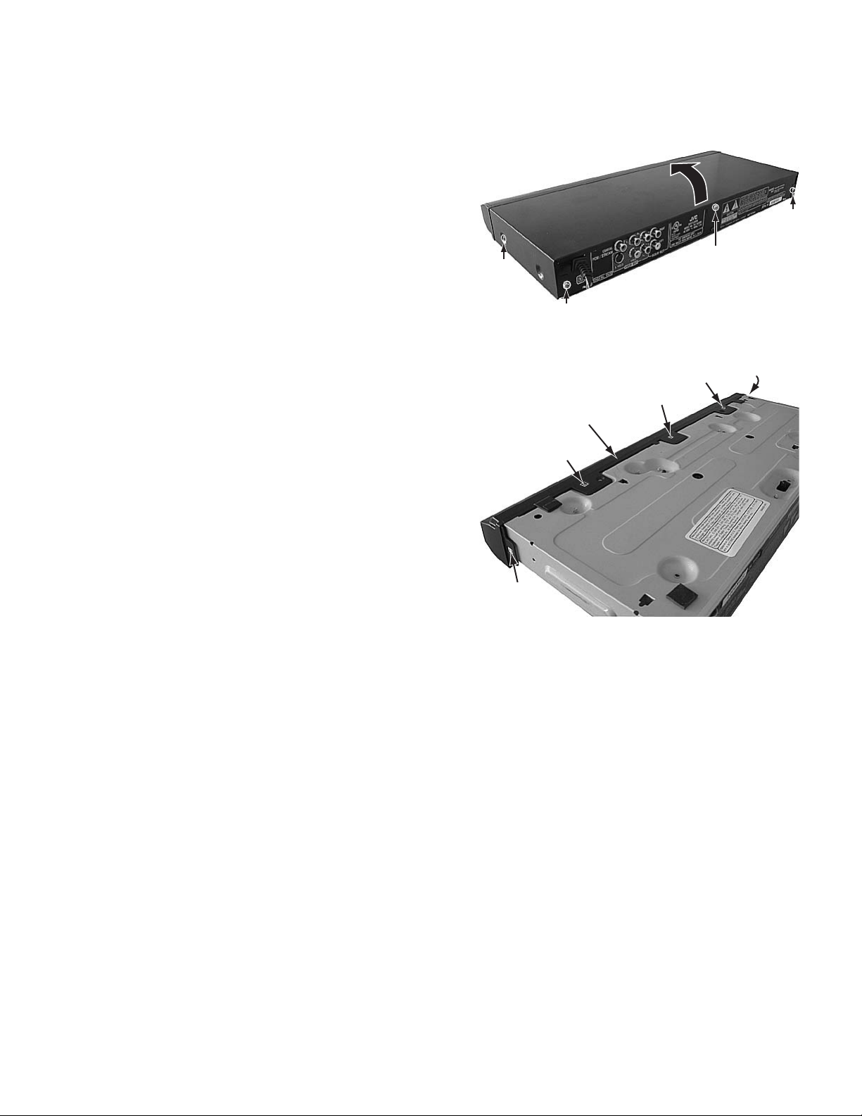
SECTION 3
TOP COVER
DISASSEMBLY
3.1 Main body section
3.1.1 Removing the top cover (See Figure 1)
(1) Remove the two screws A attaching the top cover on both
sides of the main body.
(2) Remove the three screws B attaching the top cover on the
back of the main body.
(3) Raise the both sides and lower part of the rear of the top
cover, with opening them slightly in an outward direction.
And the top cover will be removed.
3.1.2 Removing the front panel assembly (See Figure 2)
• Prior to performing the following procedure, remove the top
cover.
• There is no need to remove the mechanism assembly.
(1) Hook a and b are removed respectively, and the front panel
assembly is removed.
A x 2
B
Front panel
assembly
Hook b
TOP COVER
TOP COVER
Fig.1
Hook b
Hook b
B
B
Hook a
Hook a
Fig.2
(No.YD095)1-9
Page 10
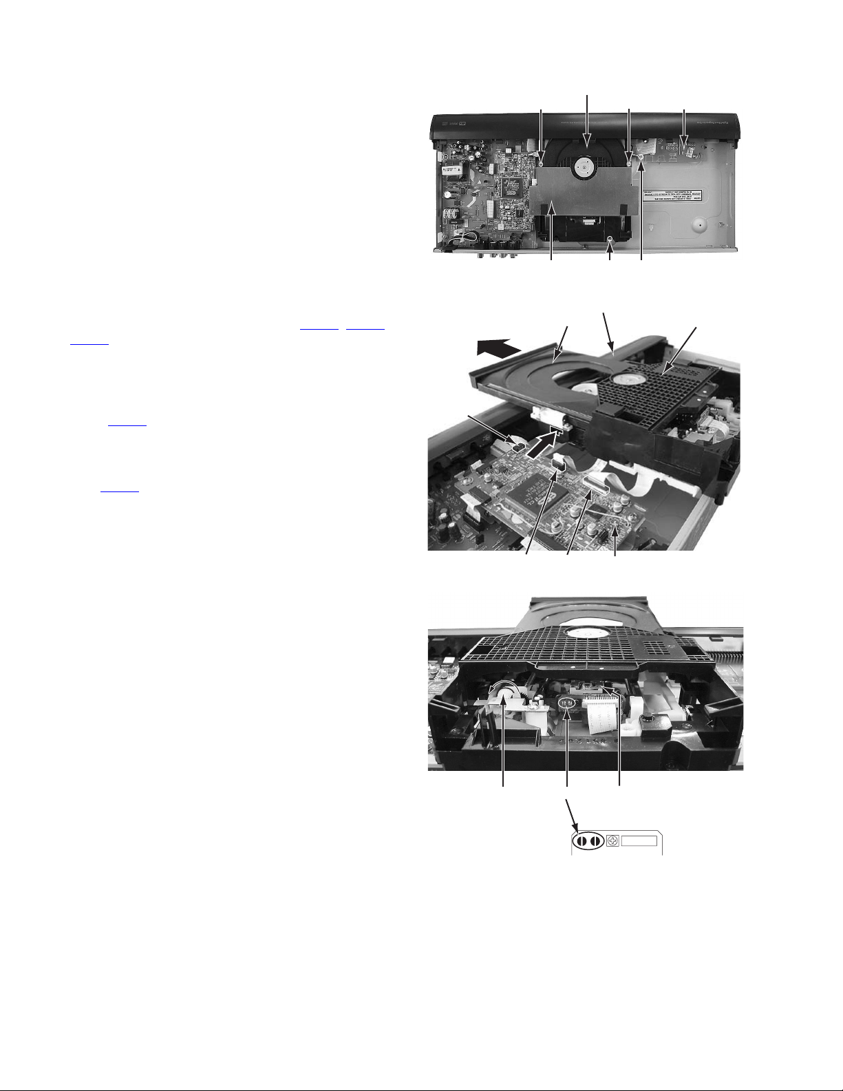
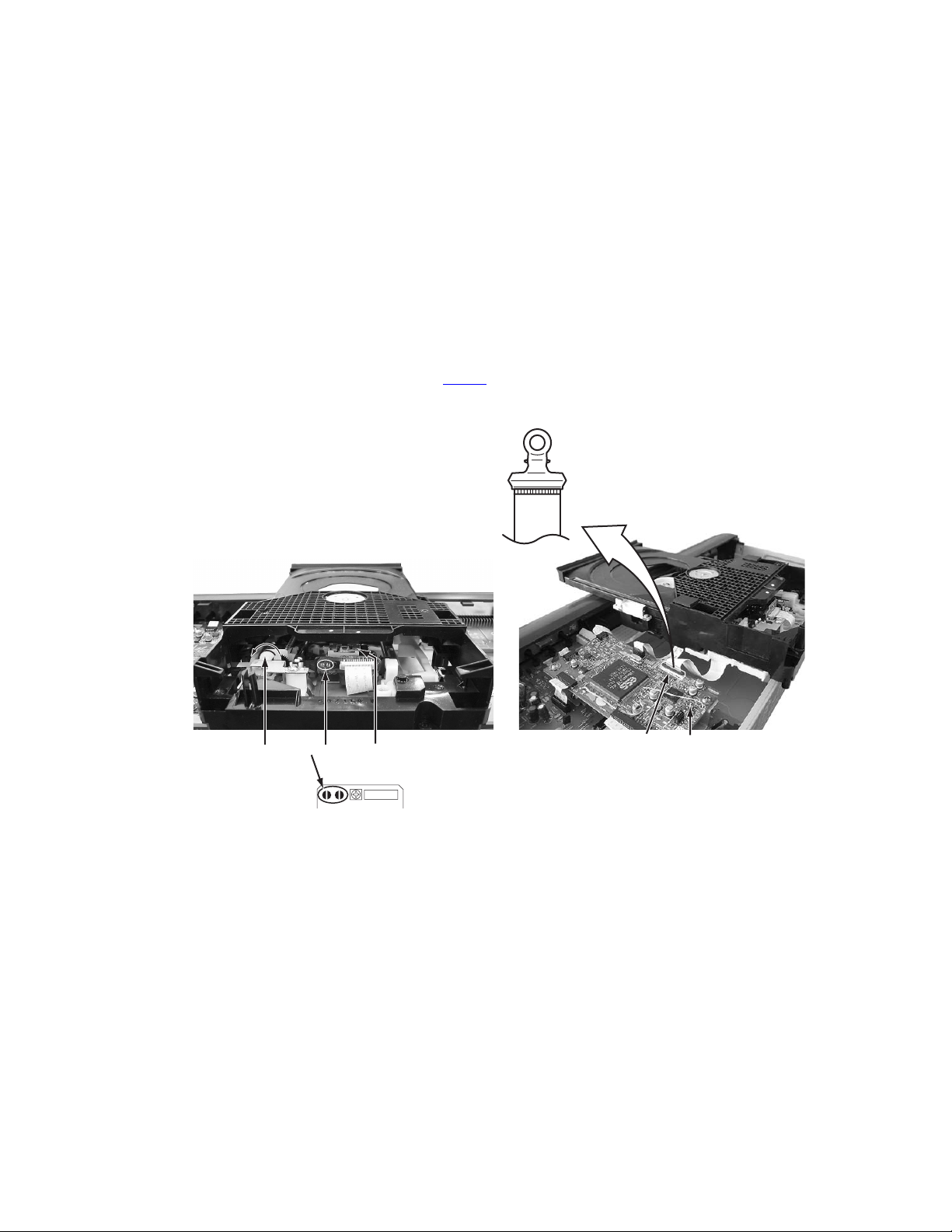
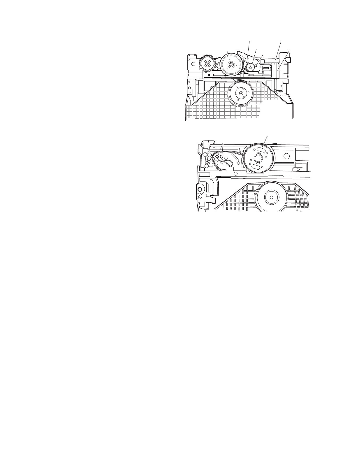
3.1.3 Removing the mechanism assembly (See Figure 3, Figure 4, Figure 5)
Push
• Prior to performing the following procedure, remove the top
cover.
• There is no need to remove the front panel assembly.
(1) Remove the three screws C attaching the mechanism as-
sembly and shield.
(2) Remove the one screw G attaching the FL Display board
and lug wire.
(3) Remove the mechanism assembly by lifting the rear part of
the mechanism assembly.
(4) Insert a kind of screwdriver in a hole located in the right
side of mechanism assembly, and push a lever until it can-
not be inserted any further.
(5) A tray is made to slide ahead.
(6) A gear 1 is turned counterclockwise. Then, a pick-up unit
moves back.
(7) It solders to two c sections on the pick-up unit.
(8) Disconnect the card wire from connector CN201
on the digital board.
CN101
ATTENTION:
Please extract the wire after short-circuited of two places
on the pick-up unit in part c with solder. Please remove
the solder two places of part c after connecting the wire
with CN101
CAUTION:
Be sure to solder the short land sections “c” on the pickup unit before disconnecting the card wire from connector CN101
If the card wire is disconnected without attaching solder,
the pick-up unit may be destroyed by static electricity.
when reassembling.
on the digital board.
, CN202,
CN202
Mechanism assembly
C
Shield
C
Fig.3
Front panel assembly
Tr ay
Push
FL Display board
C
G
Mechanism assembly
CN201 CN101 Digital board
Fig.4
Gear1
Part c
Fig.5
Pick-up
1-10 (No.YD095)
Page 11
3.1.4 Removing the rear panel (See Figure 6 )
• Prior to performing the following procedure, remove the top
cover.
(1) Remove the four screws D attaching the rear panel.
(2) Disconnect the power cord from connector P901
main board
on the
Main board
3.1.5 Removing the digital board and main board. (See Figure 7 ,Figure 8)
• Prior to performing the following procedure, remove the top
cover/front panel assembly/rear panel.
(1) Remove the two screws E attaching the digital board.
(2) Disconnect the card wire from connector CN201
, CN301, CN302, CN303 on the digital board.
CN101
(3) Disconnect the card wire from connector CN903 on the
main board.
(4) Remove the four screws F attaching the main board.
, CN202,
CN301
CN302
F
P901
CN202
CN303
E
Digital board
CN903
F
D
CN101
E
CN201
Fig.6
Fig.7
Rear panel
D
3.1.6 Remove the FL Display board (See Figure 9)
• Prior to performing the following procedure, remove the top
cover.
(1) Disconnect the card wire from connector CN501
Display board.
(2) Remove the two screws G attaching the FL Dispiay board.
on the FL
F
Main board
F
Fig.8
CN501
G G
FL Display board
Fig.9
(No.YD095)1-11
Page 12
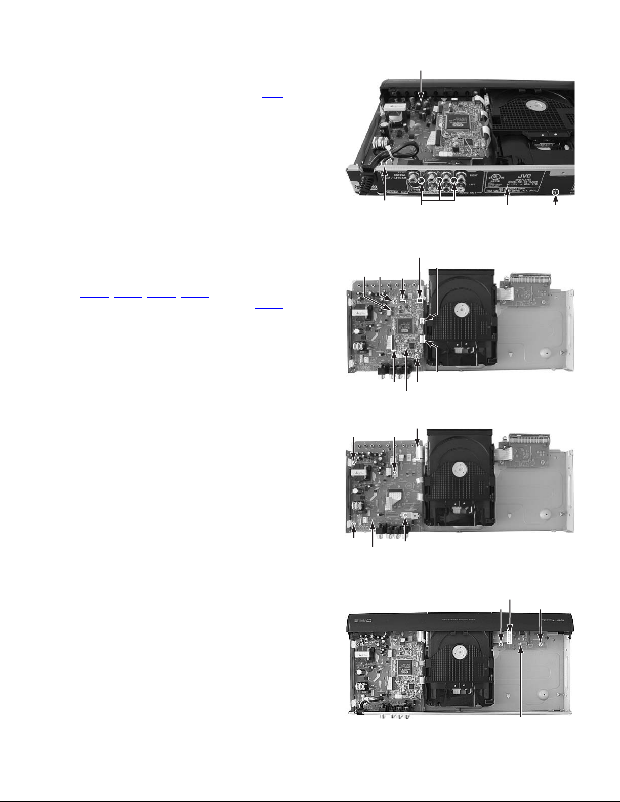
3.2 Loading mechanism assembly
Projection of the tray
3.2.1 Removing the tray (See Figure 1, Figure 2, Figure 3, Figure 4, Figure 5, Figure 6)
(1) Push a of the slide cam on the hole in the right side of the
loading base by using a driver until it stops. (See Figure 1.)
(2) The tray comes out. Pull the tray in a front direction until it
stops.
(3) Remove the two screws A attaching the slide bracket. (See
Figure 2.)
(4) Tilt the tray in a direction of the arrow around the point in
the left rear part of the tray. (See Figure 3.)
(5) The rail of the tray is removed from b of the loading base.
Then, remove the tray upward. (See Figure 4.)
Attaching the tray:
Engage c of the loading base to the projection of the tray while
tilting the tray to the left. Turn the tray in a direction of the arrow, and attach the slide bracket. (See Figure 5.)
Note:
Prior to the procedure above, move the slide cam in a direction
of the arrow so that d of the slide cam can be inserted in e of
the tray. (See Figure 6.)
Tray
The point in the left rear part
Tray
Fig.3
Push
Slide cam part a
Slide bracket
A
Fig.1
Fig.2
A
Loading base
Tray
Loading base part b
Rail of the tray
Fig.4
Projection of the tray
Loading base part c
Fig.5
Par t e
1-12 (No.YD095)
Par t d
Slide cam
Fig.6
Page 13
3.2.2 Removing the traverse mechanism assembly (See Figure 6)
f
Shaft
(1) Reverse the loading mechanism assembly.
(2) A card wire is removed from a wire bracket.
(3) Remove the four screws B attaching the traverse mecha-
nism assembly. Remove the traverse mechanism assembly upward.
Loading mechanism assembly
3.2.3 Removing the elevator (See Figure 8 and Figure 9)
• Prior to the following procedure, remove the traverse mechanism assembly.
(1) Remove the two arms of the elevator from the two parts f
by moving the arms in a direction of the arrow.
(2) Pull out the elevator in a rear direction.
Attaching the elevator:
Engage the two holes g to the two shafts on the front part of
the elevator. And then, attach the elevator.
B
B
B
wire
bracket
B
Traverse mechanism assembly
Fig.7
Elevator
Part f
Fig.8
g
Slide cam
Elevator
Shaft
Fig.9
(No.YD095)1-13
Part
g
Page 14
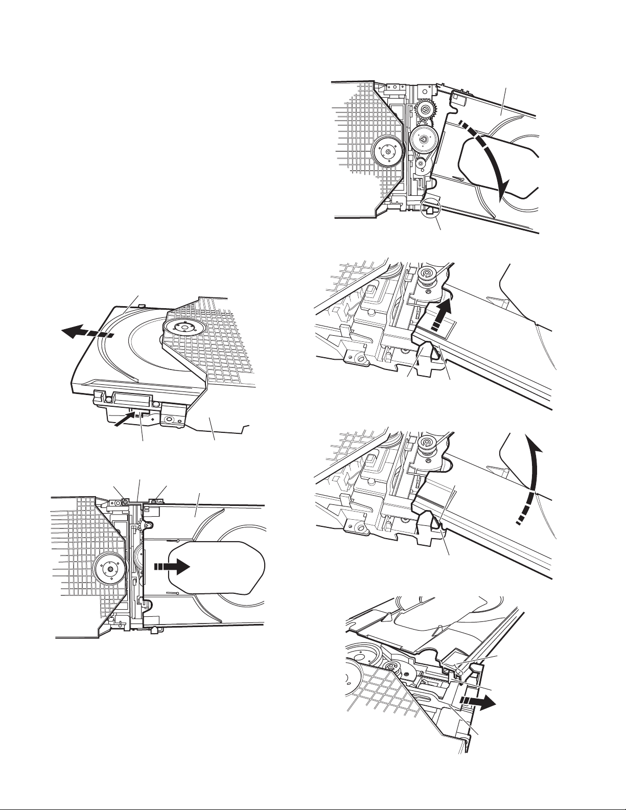
3.2.4 Removing the loading motor (See Figure 10 and Figure 11)
• Prior to the following procedure, remove the tray, the traverse
mechanism assembly, and the elevator.
(1) Remove the belt from the pulley.
(2) Remove two screws C attaching the loading motor.
(3) Remove two solders h on the switch board.
Switch board
Pulley
Part
Pulley
㧯
Loading base
Slide cam
Belt
㧯
Fig.10
Loading motor
h
Fig.11
1-14 (No.YD095)
Page 15

3.3 Traverse mechanism assembly
3.3.1 Removing the pickup (See Figure 12, Figure 13)
• Prior to the following procedure, remove the traverse mechanism assembly.
(1) Remove one screw D attaching the plate.
(2) Remove the plate and the leaf spring.
(3) Lift i of the shaft 1, and pull out the shaft 1 from j.
(4) Remove k of the pickup from the shaft 2.
Attaching the pickup:
(1) Engage k of the pickup to the shaft 2.
(2) A spring is lifted and shaft 1 is inserted in the j, and at-
tach the shaft 1 to i.
(3) Attach the leaf spring, and then attach the plate. Fix the
leaf spring and the plate by using the screw D.
spring
D
Leaf spring
Plate
Fig.12
Part j
spring
Shaft 2
Part k
Shaft 1
Part i
Fig.13
(No.YD095)1-15
Page 16

SECTION 4
ADJUSTMENT
4.1 Test mode setting method
(1) Unplug the power plug.
(2) Insert power plug into outlet while pressing both "PLAY" key and "STOP" key of the main body.
(3) The FL display shows "N330 ∗∗ ", and the main body turns to test mode.
*The portion of "∗∗" changes with destinations.
(4) To release test mode, press "POWER" key of the main body.
NOTE:
Each pressing of "SET UP" key of the remote controller in test mode changes the mode as follows.
Message area of TV screen
N330 ---------------
-------------
-------------
-------------
Becomes test mode ----
Version of backend -----
Type of flash memory
Version of frontend -----
FL Display becomes all lighting
CHCK -------------------
Check mode --------------
TEST MODE
BE VERSION :
FE VERSION :
CHECK MODE
TV screen
TEST MODE
Message area
4.2 Initialization method
Please initialize according to the following procedures in the following case :
• Just after you update the firmware
• After you confirm the symptoms that a customer points out. First initialize, and then confirm whether the symptoms are improved or
not.
• After servicing, before returning the main body to a customer. (Initialized main body should be returned to a customer.)
(1) Set the main body at test mode.
(2) Press "FWD SKIP" key of the main body.
(3) When indicate "P" on the FL display, initialization is completed.
PLAY key
STANDBY/ON
OPEN/
CLOSE
+
SLOW
DISPLAYON SCREEN
T
O
P
M
E
N
U
ENTER
M
E
N
U
SELECT
CLEAR
123
456
789
CANCEL RETURN
0
SOUND
TITLE/
VFP
EFFECT
GROUP DIMMER
I/P
SUBTITLEANGLE
AUDIO
SLIDE EFFECT
T
H
U
M
B
N
A
IL
/
L
IS
T
SET UP key
S
E
T
U
P
(switch of mode)
NEXTPREVIOUS
ZOOM
POWER key
(for test mode)
FWD SKIP key
(for initialize)
STOP key
(for test mode)
1-16 (No.YD095)
FL Display
Page 17

4.3 Updating of firmware
When firmware update is necessary,information is available from the website of DIGITAL VIDEO STORAGE CATEGORY,CS group.
4.3.1 Distribution method
(1) Compressed file is distributed through JS-NET.
(2) Download the version of the destination of the model, and self-extract the file.
(3) "N330XXXX.rom" file is made.(The portion of “XXXX” may change with a model and destinations.)
(4) Write "N330XXXX.rom" file in the root of CD-R/RW. (Folders such as jvc_dvd are not necessary.)
4.3.2 Update method
(1) Prepare update disc with "N330XXXX.rom" file written in its root.
(2) Press "POWER" key of the main body to turn the main body on.
(3) Insert the update disc.
(4) The contents of disc are read automatically and update is started.
(5) TV screen 1/27,2/27... if the count-up is displayed and it becomes 27/27, it will be displayed on FL display as "DONE", and up-
date will be completed.
(6) When update finishes, the main body changes from the POWER ON mode to STANDBY mode.
(7) Press the "OPEN/CLOSE" key, and open the tray to eject the disc.
(8) Set the main body at test mode, and perform initialization. Then, confirm the version of the firmware.
(No.YD095)1-17
Page 18

4.4 Confirm method of operation
Please confirm the operation of the undermentioned item after doing the repair and the upgrade of the firmware.
Initialize Refer to the initialization method.
Muting working The noise must not be had to the performance beginning when you push "PLAY" button or
at ON/STANDBY.
FL Display The mark and the logo, etc. displayed by each operation must be displayed correctly.
FL Display should light correctly without any unevenness.
All Function button All function buttons should worked correctly with moderate click feeling.
Open and close movement of tray When press OPEN/CLOSE button the tray should move smoothly without any noise.
Remote controller unit working Check the correctly operation in use of remote controller unit.
Reading of TOC Be not long in the malfunction.
Search Both forward-searches and backward-searches should be able to be done.Do not stop be
searching or after the search.
Skip Both forward-skip and backward-skip should be able to be done.Do not stop be after the skip.
Playback Do not find abnormality etc. of tone quality and the picture quality.
Most outside TITLE playback check Play VT-501 TITLE 59 CHAPTER 1 , check normal playback.
1-18 (No.YD095)
Page 19

5.1 Servo volume
Press OPEN
/CLOSE key
SECTION 5
TROUBLESHOOTING
Is tray
operation
Confirmation of tray drive circuit
N
and circuit in surrounding
correct?
Y
Is the traverse moving
along the innermost
N
perimeter for SW detection?
Y
"NO DISC" message appears
Y
immediately after vertical
movement of the pick-up lens
N
The state that DISC does not rotate continues for
several seconds, and becomes NO DISC or an
error display afterwards.
The rotation of DISC becomes high-speed and
abnormal, and becomes NO DISC or an error
display afterwards.
N
Is focus retraction OK?
FE
OFF
Even when it retracts
correctly, if it is out of focus
and makes repeated retries
with a clicking sound, it is
in error.
ON
See "5.2.4 Focus ON error"
N
in "Check points for
individual errors"
Y
Is tracking retraction OK?
See "5.2.3 Traverse movement error"
in "Check points for individual errors"
See "5.2.2 Disk detection, distinction error"
in "Check points for individual errors"
Y
See "5.2.1 Spindle start error"
in "Check points for individual errors"
Is the inter-layer jump OK?
FE
LO LI
A
Two layers of DVD only.
N
5.2.8 Inter-layer
jump error
Y
TE
OFF
If TE waveform reappears
or fails to converge after the
TE retraction, it is in error.
ON
Y
Is the spindle servo
locked correctly?
Is the RF OUT waveform
locked correctly?
Y
A
See "5.2.5 Tracking ON error"
N
in "Check points for
individual errors"
See "5.2.6 Spindle CLV error"
N
in "Check points for
individual errors"
Fig.1
Has the disc information
been collected?
Stop will result
Y
Is playback
N
possible?
Y
OK !
N
5.2.
7 Address
read error
Check 5.2.9 to 5.2.12
items in "Check points
for individual errors"
(No.YD095)1-19
Page 20

5.2 Check points for each error
5.2.1 Spindle start error
(1) Defective spindle motor
• Are there several ohms resistance between each pin of CN201
(The power supply is turned off and measured.)
(2) Defective spindle motor driver (IC201
• Has motor drive voltage of a sine wave or a rectangular wave gone out to each terminal(UOUT,VOUT,WOUT)
of CN201
• Is FG pulse output from the terminal of IC201"41"(FG) according to the rotation of the motor?
(3) Has the control signal come from the microcomputer?
• Is it "H" while the terminal of IC201
• Is the control signal input to the terminal of IC201"25"(SPDRV)?
• Is the SVREF voltage input to the terminal of IC201
(4) Is the FG signal input to the servo IC?
• Is FG pulse input to the terminal of IC301
5.2.2 Disc Detection, Distinction error (no disc, no RFENV)
• Laser is defective.
• Front End Processor is defective (IC101
• APC circuit is defective. --- Q101, Q102.
• Pattern is defective. --- Lines for CN101
• IC101 --- For signal from IC101 to IC301, is signal output from IC101 "40" (FE)?
5.2.3 Traverse movement error
(1) Defective traverse driver
• Has the voltage come between terminal of CN201
(2) Defective BTL driver (IC201)
• Has the motor drive voltage gone out to IC201"11" or "14"?
(3) Has the control signal come from the microcomputer?
• TRSDRV Is the signal input? (IC301
(4) TRVSW is the signal input to microcomputer? (IC301 "177")
5.2.4 Focus ON error
• Is FE output ? --- Pattern, IC101
• Is FODRV signal sent ? (R275) --- Pattern, IC301 "160"
• Is driving voltage sent ?IC101 "3", "4" --- If NG, pattern, driver, mechanical unit .
• Mechanical unit is defective.
5.2.5 Tracking ON error
• When the tracking loop cannot be drawn in, TE shape of waves does not settle.
• Mechanical unit is defective.
Because the self adjustment cannot be normally adjusted, the thing which cannot be normally drawn in is thought.
• Periphery of driver (IC201
Relative component or IC it self is defective.
• Microcomputer (IC301
When improperly adjusted due to defective IC.
"2,3,4" and IC201"19,18,17"?
)
)
)
"48"(MUTE1) is operating?
"26"(VREF)?
"175"(FGIN) according to the rotation of the motor?
).
- All patterns which relate to pick-up and patterns between IC101
"7" and "8" ?
"161")
"2-3","3-4","2-4"?
1-20 (No.YD095)
Page 21

5.2.6 Spindle CLV error
• IC101
• Does not the input or the output of driver's spindle signal do the grip?
• Has the tracking been turned on?
• Spindle motor or driver is defective.
• Additionally, "IC101
5.2.7 Address read error
• Besides, the undermentioned cause is thought though specific of the cause is difficult because various factors are thought.
5.2.8 Between layers jump error (double-layer disc only)
• Mechanism defective
• Defect of driver's IC(IC201
• Defect of microcomputer(IC301
5.2.9 Neither picture nor sound is output
5.2.10 Picture is distorted or abnormal sound occurs at intervals of several seconds.
• Is the feed operation normal?
• Are not there caught of the feeding mechanism etc?
5.2.11 Others
• The image is sometimes blocked, and the image stops.
• The image is blocked when going to outer though it is normal in surroundings in the disk and the stopping symptom increases.
There is a possibility with bad jitter value for such a symptom.
5.2.12 CD During normal playback operation
-- "55"(DIN), "54(DIP).
and IC301" and "Mechanism is defective(jitter)", etc. are thought.
Mechanism is defective. (jitter)
IC301
The disc is dirty or the wound has adhered.
)
)
(1) It is not possible search
• Has the tracking been turned on?
• To "(5.2.5) Tracking ON error" in "Check points for each error" when the tracking is not normal.
• Is the feed operation normal?
To "(5.2.3) traverse movement error" in "Check points for each error" when it is not normal.Are not there caught of the feeding
mechanism etc?
(1) Is TOC reading normal?
• Displays total time for CD-DA.
• Shifts to double-speed mode for V-CD
(2) Is playback afterwards possible?
(3) When can not do a normal playback
• --:-- is displayed during FL search.
According to [It is not possible to search ] for DVD (5.2.9), check the feed and tracking systems.
• No sound is output although the time is displayed.(CA-DA)
DAC, etc, other than servo.
• The passage of time is not stable, or picture is abnormal.(V-CD)
• The wound of the disc and dirt are confirmed.
(No.YD095)1-21
Page 22

Victor Company of Japan, Limited
DIGITAL VIDEO STORAGE CATEGORY 12, 3-chome, Moriya-cho, kanagawa-ku, Yokohama, kanagawa-prefecture, 221-8528, Japan
(No.YD095)
Printed in Japan
VPT
Page 23

PARTS LIST
[XV-N330BUS,XV-N330BUC,XV-N330BUJ,
XV-N332SUS,XV-N332SUC,XV-N332SUJ]
* All printed circuit boards and its assemblies are not available as service parts.
* (x_) in a description column shows the number of the used part.
Area Suffix
US ----------------------- U.S.A.
UC ------------------- Canada
UJ ------------ U.S.A Militaly
- Contents -
Exploded view of general assembly and parts list
DVD Traverse mechanism assembly and parts list
DVD Loading mechanism assembly and parts list
Electrical parts list
Packing materials and accessories parts list
3-2
3-4
3-6
3-8
3-12
(No.YD095)3-1
Page 24

Exploded view of general assembly and parts list
38
36
37
Block No.M1MM
Main
board
Digital
7
board
9
4
13
16
15
2
3
FRONT
SIDE
Operation
switch board
17
a
1
b
c
37
37
25
10
26
26
27
9
8
8
39
"A"
VFD board
11
9
38
5
32
31
30
29
"A" BACK SIDE
28
35
33
!
6
7
12
a
23
b
24
c
"A" BACK SIDE
21
19
21
34
18
19
14
!
21
20
21
20
22
3-2(No.YD095)
Page 25

General assembly
Block No. [M][1][M][M]
Symbol No. Part No. Part Name Description Local
1 GN10059-039A FRONT PANEL 330UC,330US
1 GN10059-043A FRONT PANEL 330UJ
1 GN10059-040A FRONT PANEL 332UC,332US
1 GN10059-044A FRONT PANEL 332UJ
2 GN40020-002A JVC MARK
3 GN20111-001A WINDOW SCRREN
4 GN20201-001A PUSH BUTTON only 330
4 GN20201-002A PUSH BUTTON only 332
5 QYSDSF2608ZA TAP SCREW FOR PUSH BUTTON(x3)
6 GN10061-001A CHASSIS BASE
7 GN40054-002A FELT SPACER REAR FOOT(x2)
8 QYSBSGG3006EA TAP SCREW VFD CB+CHASSIS(x2)
9 QYSBSGG3006EA TAP SCREW MAIN+CHASSIS(x4)
10 GN30126-001A BRACKET (x2) except ver.UJ
10 GN30116-001A BRACKET (x2) only ver.UJ
11 QYSBSGG3006EA TAP SCREW DIGITAL CB+BRACKET(x2)
12 QUQ210-0520CC-E FFC WIRE MECHA TO DIGITAL
13 QQR1609-001 F.CORE except ver.UJ
14 QUQ210-2306CJ-E FFC WIRE MAIN TO DIGITAL
15 QUQ210-1303CJ-E FFC WIRE MAIN TO DIGITAL
16 QUQ210-0703CJ-E FFC WIRE MAIN TO DIGITAL
17 QUQ212-1724CJ-E FFC WIRE VFD TO MAIN
18 ------------ TRAVERSE MECHANISM
19 LE40900-003A INSULATOR (x2)
20 LE40900-005A INSULATOR (x2)
21 LE40901-002A SPECIAL SCREW FOR INSULATOR(x4)
22 ------------ LOADING MECHANISM
23 GN30102-001A FFC HOLDER FOR FFC WIRE
24 QYSDSF2608ZA TAP SCREW FFC HOLDER
25 GN30006-027A SPACER (x2)
26 QYSBSG3006ZA TAP SCREW MECHA+CHASSIS(x3)
27 GN30082-001A SHIELD except ver.UJ
28 GN20115-060A REAR PANEL 330UC,330US
28 GN20115-066A REAR PANEL 330UJ
28 GN20115-061A REAR PANEL 332UC,332US
28 GN20115-067A REAR PANEL 332UJ
29 QYSBSGY3008MA TAP SCREW REAR+CHASSIS
30 QYSBSGY3008MA TAP SCREW AUDIO
31 QYSBSGY3008MA TAP SCREW VIDEO
32 QYSBSGY3008MA TAP SCREW COAXIAL
33 QMF5AU1-1R6-J1 FUSE 1.6A AC125V except ver.UJ
33 QMF5AE2-1R6-J1 FUSE 1.6A AC250V only ver.UJ
34 QMPD590-170-JN POWER CORD(US/CA) 1.7m BLACK except ver.UJ
34 QMPK370-170-JN POWER CORD(EU) 1.7m BLACK only ver.UJ
35 LV44670-001A TIE BAND
36 GN20114-001A TOP COVER only 330
36 GN20114-002A TOP COVER only 332
37 QYSBSGG3006EA TAP SCREW REAR(x3)
38 QYSDSG3008MA TAP SCREW SIDE(x2) only 330
38 QYSDSG3008NA TAP SCREW SIDE(x2) only 332
39 GN20202-001A FITTING only 330
39 GN20202-002A FITTING only 332
(No.YD095)3-3
Page 26

DVD Traverse mechanism assembly and parts list
Grease
=JVG-31N
=CFD-4007ZY2
=PG-641
=1401C
< Back side >
25
24
GXL-G11-1C
26
Block No.M2MM
23
22
21
A
17
A
14
13
15
12
10.5mm
+
-
2
0.1mm
27
3
16
27
+
27
20
19
18
5
8
11
9
6
7
4
10
63.3mm
11
0.1mm
-
3-4(No.YD095)
1
Page 27

DVD Traverse mechanism
Symbol No. Part No. Part Name Description Local
1 LE20729-002A MECHA BASE
2 LE20731-002A SPINDLE BASE
3 QYSDST2605ZA TAP SCREW M2.6 x 5mm(x2)
4 LE40931-001A SHAFT
5 LE40995-001A BAR SPRING
6 QYSPSTU2080ZA TAP SCREW M2 x 8mm
7 LE20730-002A FEED HOLDER
8 QAR0165-001 FEED MOTOR
9 LV41510-001A FEED GEAR T
10 QYSPSPU2040ZA SCREW M2 x 4mm(x2)
11 QYSDST2605ZA TAP SCREW M2.6 x 5mm(x3)
12 QAL0786-002 P.UP
13 LE20732-001A SW ACTUATOR
14 LE31093-001A LEAD SPRING
15 QYSPSFU1740ZA TAP SCREW M1.7 x 4mm(x2)
16 QUQK05-2420AC-E FFC WIRE 24pin 20cm
17 LE40931-001A SHAFT
18 LE40855-002A FEED GEAR E
19 LV41517-003A LEAD SCREW
20 LE40930-001A FEED GEAR M
21 LE40928-002A THURUST SPRING
22 LE40927-002A PLATE
23 QYSDST2614ZA TAP SCREW M2.6 x 14mm
24 QAR0346-001 S.MOTOR
25 QYSPSPU1760ZA SCREW M1.7 x 6mm(x3)
26 LE40994-001A T.SPRING
27 LE40858-002A SPECIAL SCREW (x4)
Block No. [M][2][M][M]
(No.YD095)3-5
Page 28

DVD Loading mechanism assembly and parts list
Block No.M3MM
18
20
19
17
14
22
ELM-J2-2C
5
13
16
3
21
Grease
JVG-31N
4
JVS-1003
1
12
0.10mm
-
+
11
(All circumferences)
10
8
9
7.95mm
Back side
7
a
b
6
Switch board
a
b
3-6(No.YD095)
Page 29

DVD Loading mechanism
Symbol No. Part No. Part Name Description Local
1 LE10275-006A LOADING BASE
3 LE31043-001A PULLEY GEAR
4 LE31042-001A MIDDLE GEAR
5 LE20665-005A SLIDE CAM
6 LE20666-003A ELEVATOR
7 LE10276-003A TRAY
8 LE31045-001A BUSHING
9 LE40898-001A SHAFT
10 QYSSSF2008ZA TAP SCREW M2 x 8mm
11 QAR0197-001 MOTOR
12 LV42087-002A MOTOR PULLEY
13 QYSPSPU1730ZA SCREW M1.7 x 3mm(x2)
14 QYSDSF2008ZA TAP SCREW M2 x 8mm(x2)
16 LE40897-001A BELT
17 LE31046-003A CLAMPER
18 LV42930-003A P.C.MAGNET
19 LE40899-001A YOKE
20 LE40906-002A SPECIAL SCREW
21 LE31044-001A IDLE GEAR
22 LE40937-003A LEAF SPRING
Block No. [M][3][M][M]
(No.YD095)3-7
Page 30

Electrical parts list
Main board
Block No. [0][1]
Symbol No.
IC501 PT6315-S IC
IC502 GP1UE291QKVF IR UNIT
IC701 RC4558D-X IC
IC704
IC901 MIP2C50MSSCF IC
IC902 TL432/A/-T IC
IC902 or MM1530AT-T IC
Q701 RT1N44HC-X DIGI TRANSISTOR
Q701 or KRC109S-X TRANSISTOR
Q702 2SC3928A/QR/-X TRANSISTOR
Q702 or 2SC2412K/RS/-X TRANSISTOR
Q703
Q703 or 2SC3928A/QR/-X TRANSISTOR
Q704 RT1P141C-X DIGI TRANSISTOR
Q704 or KRA102S-X DIGI TRANSISTOR
Q705
Q705 or 2SC3928A/QR/-X TRANSISTOR
Q760 RT1P44QC-X DIGI TRANSISTOR
Q951 2SC3576-JVC-T TRANSISTOR
Q952 RT1P441C-X DIGI TRANSISTOR
Q952 or KRA104S-X DIGI TRANSISTOR
D504 1SS133-T2 SI DIODE
D505 1SS133-T2 SI DIODE
D506 1SS133-T2 SI DIODE
D507 1SS133-T2 SI DIODE
D701 MA111-X SI DIODE
D701 or 1SS355-X SI DIODE
D702 MA111-X SI DIODE
D702 or 1SS355-X SI DIODE
D703 MA111-X SI DIODE
D703 or 1SS355-X SI DIODE
D704 MA111-X SI DIODE
D704 or 1SS355-X SI DIODE
D705 MA111-X SI DIODE
D705 or 1SS355-X SI DIODE
D902 1F4G-T2 FR DIODE
D902 or 1F4G-G-T2 FR DIODE
D903 DI106 BRIDGE DIODE
D905 1F4G-T2 FR DIODE only ver.UJ
D905 or 1F4G-G-T2 FR DIODE only ver.UJ
D906 1SS133-T2 SI DIODE except ver.UJ
D906 1SS244-T2 SI DIODE IM only ver.UJ
D951 1F4G-T2 FR DIODE
D951 or 1F4G-G-T2 FR DIODE
D952 1F4G-T2 FR DIODE
D952 or 1F4G-G-T2 FR DIODE
D953 SB240-F26 SB DIODE
D954 PS154R-F83 FR DIODE
D955 PS154R-F83 FR DIODE
D956 1F4G-T2 FR DIODE
D956 or 1F4G-G-T2 FR DIODE
D957 1F4G-T2 FR DIODE
D957 or 1F4G-G-T2 FR DIODE
D960 MTZJ3.6B-T2 S.B.DIODE
PC901 PC123Y82FZ PHOTO COUPLER
C501 NCF31EZ-104X C CAPACITOR 0.1uF 25V Z except ver.UJ
C501 NRSA63J-0R0X MG RESISTOR 0Ω 1/16W J only ver.UJ
C502 NCF31CZ-104X C CAPACITOR 0.1uF 16V Z
C503 NCF31EZ-104X C CAPACITOR 0.1uF 25V Z except ver.UJ
C503 NRSA63J-0R0X MG RESISTOR 0
C506 QETN0JM-107Z E CAPACITOR 100uF 6.3V M
C507 NCF31CZ-104X C CAPACITOR 0.1uF 16V Z
C508 NCB31HK-223X C CAPACITOR 0.022uF 50V K
C509 NCB31HK-472X C CAPACITOR 4700pF 50V K
C510 NCB31HK-472X C CAPACITOR 4700pF 50V K
C511 NCF31CZ-104X C CAPACITOR 0.1uF 16V Z
C515 NCF31CZ-104X C CAPACITOR 0.1uF 16V Z
C701 NCB31HK-472X C CAPACITOR 4700pF 50V K
Part No. Part Name Description Local
SN74AHCT08NS-X
2SC2412K/QRS/-X
2SC2412K/QRS/-X
IC
TRANSISTOR
TRANSISTOR
Ω
1/16W J only ver.UJ
Symbol No.
C702 NCB31HK-471X C CAPACITOR 470pF 50V K
C706 QETN1EM-106Z E CAPACITOR 10uF 25V M
C707 QFN31HJ-101Z M CAPACITOR 100pF 50V J
C708 NCB31HK-152X C CAPACITOR 1500pF 50V K
C709 NCB31HK-472X C CAPACITOR 4700pF 50V K
C710 NCB31HK-471X C CAPACITOR 470pF 50V K
C711 NCB31HK-471X C CAPACITOR 470pF 50V K
C712 QETN1EM-106Z E CAPACITOR 10uF 25V M
C713 QFN31HJ-101Z M CAPACITOR 100pF 50V J
C714 NDC31HJ-470X C CAPACITOR 47pF 50V J
C715 NCB31HK-471X C CAPACITOR 470pF 50V K
C716 NCB31HK-271X C CAPACITOR 270pF 50V K
C717 NCB31HK-471X C CAPACITOR 470pF 50V K
C718 NDC31HJ-470X C CAPACITOR 47pF 50V J
C719 NCB31HK-271X C CAPACITOR 270pF 50V K
C720 NCB31CK-104X C CAPACITOR 0.1uF 16V K
C721 NCB31HK-332X C CAPACITOR 3300pF 50V K
C722 NCB31HK-472X C CAPACITOR 4700pF 50V K
C723 NCB31HK-332X C CAPACITOR 3300pF 50V K
C724 NCB31HK-472X C CAPACITOR 4700pF 50V K
C726 QETN1CM-107Z E CAPACITOR 100uF 16V M
C728 QETN1CM-107Z E CAPACITOR 100uF 16V M
C729 NCF31CZ-104X C CAPACITOR 0.1uF 16V Z
C730 QETN1AM-227Z E CAPACITOR 220uF 10V M
C731 NCB31HK-471X C CAPACITOR 470pF 50V K
C740 NCB31HK-271X C CAPACITOR 270pF 50V K
C741 NCB31HK-151X C CAPACITOR 150pF 50V K
C742 NCB31CK-104X C CAPACITOR 0.1uF 16V K
C744 NCB31HK-471X C CAPACITOR 470pF 50V K
C745 NCB31HK-471X C CAPACITOR 470pF 50V K
C746 NCB31HK-271X C CAPACITOR 270pF 50V K
C748 NDC31HJ-470X C CAPACITOR 47pF 50V J
C751 NCB31HK-271X C CAPACITOR 270pF 50V K
C752 NDC31HJ-270X C CAPACITOR 27pF 50V J
C753 NCB31HK-271X C CAPACITOR 270pF 50V K
C755 QETN1CM-107Z E CAPACITOR 100uF 16V M
C756 QETN1CM-107Z E CAPACITOR 100uF 16V M
C771 NDC31HJ-470X C CAPACITOR 47pF 50V J
C777 NCB31HK-332X C CAPACITOR 3300pF 50V K
C790 NCB31HK-332X C CAPACITOR 3300pF 50V K
C901 QFZ9073-823 MM CAPACITOR 0.082uF AC250V M
C903 QCZ9071-101 C CAPACITOR 100pF AC400V K
C905 QCZ9079-222 C CAPACITOR 2200pF AC250V M
C906 QCZ0136-102Z C CAPACITOR 1000pF 1kV K
C907 QEZ0826-476 E CAPACITOR 47uF except ver.UJ
C907 QEZ0707-476 E CAPACITOR 47uF only ver.UJ
C908 QCZ0302-220Z C CAPACITOR 22pF 1kV J
C909 QEZ0657-396Z E CAPACITOR 39uF
C910 NCB31CK-104X C CAPACITOR 0.1uF 16V K
C911 NCB31HK-222X C CAPACITOR 2200pF 50V K
C919 NRSA63J-0R0X MG RESISTOR 0
C950 QEZ0653-227Z E CAPACITOR 220uF 6.3V M
C952 NCB31CK-104X C CAPACITOR 0.1uF 16V K
C953 NCB31CK-104X C CAPACITOR 0.1uF 16V K
C954 QEZ0654-108Z E CAPACITOR 1000uF
C955 QEZ0655-397Z E CAPACITOR 390uF 16V M
C956 QEZ0656-826Z C CAPACITOR 82uF
C957 QEZ0656-826Z C CAPACITOR 82uF
C958 QETN1AM-227Z E CAPACITOR 220uF 10V M
C959 QETN1AM-227Z E CAPACITOR 220uF 10V M
C964 QETN1CM-107Z E CAPACITOR 100uF 16V M
C966 QETN1EM-107Z E CAPACITOR 100uF 25V M
C967 NCB31CK-105X C CAPACITOR 1uF 16V K
C980 NCF31CZ-104X C CAPACITOR 0.1uF 16V Z except ver.UJ
C980 NQR0129-002X FERRITE BEADS only ver.UJ
C982 QEZ0657-396Z E CAPACITOR 39uF
C983 QEZ0654-108Z E CAPACITOR 1000uF
C985 QETN1EM-107Z E CAPACITOR 100uF 25V M
C990 NRSA63J-0R0X MG RESISTOR 0
C990 NQR0129-002X FERRITE BEADS only ver.UJ
C991 NRSA63J-0R0X MG RESISTOR 0
R502 NRSA63J-103X MG RESISTOR 10k
R503 NRSA63J-222X MG RESISTOR 2.2k
Part No. Part Name Description Local
Ω
1/16W J
Ω
1/16W J except ver.UJ
Ω
1/16W J
Ω
1/16W J
Ω
1/16W J
3-8(No.YD095)
Page 31

Symbol No.
Part No. Part Name Description Local
Symbol No.
Part No. Part Name Description Local
R504 NRSA63J-222X MG RESISTOR 2.2kΩ 1/16W J
R508 NRSA63J-223X MG RESISTOR 22kΩ 1/16W J
R510 NRSA63J-104X MG RESISTOR 100kΩ 1/16W J
R513 NRSA63J-0R0X MG RESISTOR 0Ω 1/16W J
R514 NRSA63J-0R0X MG RESISTOR 0Ω 1/16W J
R701 NRSA63J-222X MG RESISTOR 2.2k
R703 NRSA63J-473X MG RESISTOR 47k
R704 NRSA63J-682X MG RESISTOR 6.8kΩ 1/16W J
R705 NRSA63J-122X MG RESISTOR 1.2kΩ 1/16W J
R706 NRSA63J-101X MG RESISTOR 100Ω 1/16W J
R709 NRSA63J-101X MG RESISTOR 100Ω 1/16W J
R710 NRSA63J-103X MG RESISTOR 10kΩ 1/16W J
R711 NRSA63J-471X MG RESISTOR 470Ω 1/16W J
R712 NRSA63J-104X MG RESISTOR 100kΩ 1/16W J
R713 NRSA63J-104X MG RESISTOR 100kΩ 1/16W J
R714 NRSA63J-101X MG RESISTOR 100Ω 1/16W J
R715 NRSA63J-103X MG RESISTOR 10kΩ 1/16W J
R716 NRSA63J-273X MG RESISTOR 27kΩ 1/16W J
R717 NRSA63J-473X MG RESISTOR 47kΩ 1/16W J
R718 NRSA63J-222X MG RESISTOR 2.2kΩ 1/16W J
R719 NRSA63J-822X MG RESISTOR 8.2k
R720 NRSA63J-822X MG RESISTOR 8.2k
R721 NRSA63J-822X MG RESISTOR 8.2kΩ 1/16W J
R722 NRSA63J-822X MG RESISTOR 8.2kΩ 1/16W J
R723 NRSA63J-682X MG RESISTOR 6.8kΩ 1/16W J
R724 NRSA63J-104X MG RESISTOR 100kΩ 1/16W J
R725 NRSA63J-471X MG RESISTOR 470Ω 1/16W J
R726 NRSA63J-101X MG RESISTOR 100Ω 1/16W J
R727 NRSA63J-103X MG RESISTOR 10kΩ 1/16W J
R734 NRSA63J-222X MG RESISTOR 2.2kΩ 1/16W J
R735 NRSA63J-122X MG RESISTOR 1.2kΩ 1/16W J
R736 NRSA63J-682X MG RESISTOR 6.8kΩ 1/16W J
R737 NRSA63J-222X MG RESISTOR 2.2kΩ 1/16W J
R738 NRSA63J-122X MG RESISTOR 1.2kΩ 1/16W J
R739 NRSA63J-682X MG RESISTOR 6.8kΩ 1/16W J
R741 NRSA63J-820X MG RESISTOR 82Ω 1/16W J
R753 NRSA63J-122X MG RESISTOR 1.2kΩ 1/16W J
R772 NRSA63J-621X MG RESISTOR 620Ω 1/16W J
R773 NRSA63J-621X MG RESISTOR 620Ω 1/16W J
R776 NRSA63J-100X MG RESISTOR 10Ω 1/16W J
R790 NRSA63J-102X MG RESISTOR 1kΩ 1/16W J
R901 QRL01DJ-683X OMF RESISTOR 68kΩ 1W J
R902 QRE141J-271Y C RESISTOR 270Ω 1/4W J except ver.UJ
R902 QRE141J-151Y C RESISTOR 150Ω 1/4W J only ver.UJ
R903 NRSA63J-394X MG RESISTOR 390kΩ 1/16W J
R904 NRSA63J-183X MG RESISTOR 18kΩ 1/16W J
R905 NRSA63J-103X MG RESISTOR 10kΩ 1/16W J
R906 NRSA63J-103X MG RESISTOR 10kΩ 1/16W J
R911 NRSA63J-0R0X MG RESISTOR 0Ω 1/16W J
R912 NRSA63J-0R0X MG RESISTOR 0
R932 NRSA63J-103X MG RESISTOR 10kΩ 1/16W J
R934 NRSA63J-152X MG RESISTOR 1.5k
R953 NRSA63J-151X MG RESISTOR 150
R954 NRSA63J-152X MG RESISTOR 1.5kΩ 1/16W J except ver.UJ
R954 NRSA63J-332X MG RESISTOR 3.3k
R955 NRSA63J-102X MG RESISTOR 1k
R955 NRSA63J-152X MG RESISTOR 1.5kΩ 1/16W J only ver.UJ
R956 NRSA63J-224X MG RESISTOR 220k
R957 NRSA63F-562X MG RESISTOR 5.6kΩ 1/16W F
R958 NRSA63F-332X MG RESISTOR 3.3k
R961 NRSA63J-103X MG RESISTOR 10k
R963 QRE141J-4R7Y C RESISTOR 4.7Ω 1/4W J
L701 QQL231J-2R2Y COIL 2.2uH J
L702 QQL231J-2R2Y COIL 2.2uH J
L706 QQL231J-1R0Y COIL 1uH J
L707 QQL231J-1R0Y COIL 1uH J
L709 QQL231J-2R2Y COIL 2.2uH J
L730 QQL231J-2R2Y COIL 2.2uH J
L901 QQR1384-001 LINE FILTER
L951 QQR1633-001 CHOKE COIL
L952 QQR1633-001 CHOKE COIL
L953 QQR1633-001 CHOKE COIL
L954 QQL531J-101Y COIL 100uH J
L955 QQL531J-101Y COIL 100uH J
T901 QQS0328-001 SW TRANSF except ver.UJ
T901 QQS0377-001 SW TRANSF only ver.UJ
Ω
1/16W J
Ω
1/16W J
Ω
1/16W J
Ω
1/16W J
Ω
1/16W J
Ω
1/16W J
Ω
1/16W J
Ω
1/16W J only ver.UJ
Ω
1/16W J except ver.UJ
Ω
1/16W J
Ω
1/16W F
Ω
1/16W J
CN501 QGF1208C1-17 CONNECTOR FFC/FPC (1-17)
CN901 QGF1040C1-13 CONNECTOR FFC/FPC (1-13)
CN902 QGF1040C1-07 CONNECTOR FFC/FPC (1-7)
CN903 QGF1208C1-17 CONNECTOR FFC/FPC (1-17)
CN905 QGF1040F1-23 CONNECTOR FFC/FPC (1-23)
CP950
DI501 QLF0158-001 FL TUBE
FC901 QNG0003-001Z FUSE CLIP
FC902 QNG0003-001Z FUSE CLIP
J601 QNN0784-001 PIN JACK
J602 QNN0698-001 PIN JACK
K503 NRSA63J-0R0X MG RESISTOR 0
K504 NQR0251-001X FERRITE BEADS
K511 NQR0251-001X FERRITE BEADS
K703 NQR0251-001X FERRITE BEADS
OT1 GN30117-001A FL HOLDER
P901 QGA7901C1-02 CONNECTOR W-B (1-2)
S501 QSW1120-001Z PUSH SW I.M
S502 QSW1120-001Z PUSH SW I.M
S503 QSW1120-001Z PUSH SW I.M
S504 QSW1120-001Z PUSH SW I.M
S505 QSW1120-001Z PUSH SW I.M
S506 QSW1120-001Z PUSH SW I.M
S507 QSW1120-001Z PUSH SW I.M
S508 QSW1120-001Z PUSH SW I.M
QMFZ054-1R5X-J1
FUSE 1.5A
Ω
1/16W J
Digital board
Symbol No.
IC101 ES6602SF IC
IC201 LA6502-X IC
IC301 ES6820FF IC
IC302
IC302 or
IC303
IC401 RT9164A-PG-X IC
IC403
IC961 MM1688BHBE-X IC
Q101 2SB1424/R/-W TRANSISTOR
Q101 or 2SB1424/QR/-W TRANSISTOR
Q102 2SB1424/R/-W TRANSISTOR
Q102 or 2SB1424/QR/-W TRANSISTOR
D102 MA111-X SI DIODE
D102 or 1SS355-X SI DIODE
D103 MA111-X SI DIODE
D103 or 1SS355-X SI DIODE
D271 MA111-X SI DIODE
D271 or 1SS355-X SI DIODE
C101 NCF31CZ-104X C CAPACITOR 0.1uF 16V Z
C102 NCF31CZ-104X C CAPACITOR 0.1uF 16V Z
C103 NCF31CZ-104X C CAPACITOR 0.1uF 16V Z
C106 NEAF0JM-476X E CAPACITOR 47uF 6.3V M
C107 NEAF0JM-476X E CAPACITOR 47uF 6.3V M
C109 NCB31HK-681X C CAPACITOR 680pF 50V K
C110 NCB31HK-681X C CAPACITOR 680pF 50V K
C111 NCB31HK-681X C CAPACITOR 680pF 50V K
C112 NCB31HK-681X C CAPACITOR 680pF 50V K
C113 NCB31HK-101X C CAPACITOR 100pF 50V K
C114 NCB31CK-472X C CAPACITOR 4700pF 16V K
C115 NCB31HK-103X C CAPACITOR 0.01uF 50V K
C116 NCB31HK-103X C CAPACITOR 0.01uF 50V K
C117 NCF31CZ-104X C CAPACITOR 0.1uF 16V Z
C118 NCB31CK-104X C CAPACITOR 0.1uF 16V K
C119 NCB31CK-104X C CAPACITOR 0.1uF 16V K
C120 NCB31HK-103X C CAPACITOR 0.01uF 50V K
C121 NCB31CK-473X C CAPACITOR 0.047uF 16V K
C122 NCF31CZ-104X C CAPACITOR 0.1uF 16V Z
C123 NEAF0JM-476X E CAPACITOR 47uF 6.3V M
C124 NCF31CZ-104X C CAPACITOR 0.1uF 16V Z
Part No. Part Name Description Local
HY57V641620ETP7
K4S641632H-UC75
AT49BV162AS1663
SN74AHCT174PW-X
IC(DIGITAL)
IC
IC(FLASH-PRG)
IC
Block No. [0][2]
(No.YD095)3-9
Page 32

Symbol No.
Part No. Part Name Description Local
Symbol No.
Part No. Part Name Description Local
C125 NCF31CZ-104X C CAPACITOR 0.1uF 16V Z
C126 NEAF0GM-476X E CAPACITOR 47uF 4V M
C127 NCB31CK-224X C CAPACITOR 0.22uF 16V K
C128 NDC31HJ-161X C CAPACITOR 160pF 50V J
C129 NCB31HK-822X C CAPACITOR 8200pF 50V K
C130 NCB31HK-822X C CAPACITOR 8200pF 50V K
C131 NCB31HK-471X C CAPACITOR 470pF 50V K
C137 NCB31HK-102X C CAPACITOR 1000pF 50V K
C138 NCB31HK-102X C CAPACITOR 1000pF 50V K
C140 NCB31HK-681X C CAPACITOR 680pF 50V K
C141 NCB31HK-681X C CAPACITOR 680pF 50V K
C144 NCB31HK-102X C CAPACITOR 1000pF 50V K
C146 NDC31HJ-330X C CAPACITOR 33pF 50V J
C147 NDC31HJ-330X C CAPACITOR 33pF 50V J
C148 NDC31HJ-330X C CAPACITOR 33pF 50V J
C149 NCB31HK-102X C CAPACITOR 1000pF 50V K
C151 NDC31HJ-102X C CAPACITOR 1000pF 50V J
C152 NCB31CK-104X C CAPACITOR 0.1uF 16V K
C153 NCB31CK-104X C CAPACITOR 0.1uF 16V K
C154 NCB31CK-104X C CAPACITOR 0.1uF 16V K
C155 NCB31CK-104X C CAPACITOR 0.1uF 16V K
C156 NCB31CK-104X C CAPACITOR 0.1uF 16V K
C173 NEAF0JM-476X E CAPACITOR 47uF 6.3V M
C180 NCB31HK-102X C CAPACITOR 1000pF 50V K
C181 NCF31CZ-333X C CAPACITOR 0.033uF 16V Z
C182 NCF31CZ-333X C CAPACITOR 0.033uF 16V Z
C204 NCF31CZ-104X C CAPACITOR 0.1uF 16V Z
C205 NCB31HK-121X C CAPACITOR 120pF 50V K
C207 NCB31HK-222X C CAPACITOR 2200pF 50V K
C210 NCB31CK-105X C CAPACITOR 1uF 16V K
C211 NCB31CK-223X C CAPACITOR 0.022uF 16V K
C217 NCF31CZ-104X C CAPACITOR 0.1uF 16V Z
C251 NCF31CZ-474X C CAPACITOR 0.47uF 16V Z
C256 NCF31CZ-104X C CAPACITOR 0.1uF 16V Z
C257 NCB31HK-103X C CAPACITOR 0.01uF 50V K
C258 NCB31HK-153X C CAPACITOR 0.015uF 50V K
C259 NCB31HK-153X C CAPACITOR 0.015uF 50V K
C260 NCB31HK-223X C CAPACITOR 0.022uF 50V K
C261 NCB31HK-223X C CAPACITOR 0.022uF 50V K
C262 NCB31HK-223X C CAPACITOR 0.022uF 50V K
C271 NCB31HK-561X C CAPACITOR 560pF 50V K
C272 NCB31HK-561X C CAPACITOR 560pF 50V K
C273 NCB31HK-561X C CAPACITOR 560pF 50V K
C274 NCB31HK-561X C CAPACITOR 560pF 50V K
C290 NCB31HK-153X C CAPACITOR 0.015uF 50V K
C295 NCF31EZ-104X C CAPACITOR 0.1uF 25V Z
C296 NCF31EZ-104X C CAPACITOR 0.1uF 25V Z
C297 NCF31EZ-104X C CAPACITOR 0.1uF 25V Z except ver.UJ
C310 NCF31CZ-104X C CAPACITOR 0.1uF 16V Z
C311 NCB31CK-104X C CAPACITOR 0.1uF 16V K
C312 NCB31CK-104X C CAPACITOR 0.1uF 16V K
C313 NCB31CK-104X C CAPACITOR 0.1uF 16V K
C314 NCF31CZ-104X C CAPACITOR 0.1uF 16V Z
C315 NCF31CZ-104X C CAPACITOR 0.1uF 16V Z
C317 NCB31CK-104X C CAPACITOR 0.1uF 16V K
C318 NCF31CZ-104X C CAPACITOR 0.1uF 16V Z
C319 NCF31CZ-104X C CAPACITOR 0.1uF 16V Z
C320 NEAF0GM-476X E CAPACITOR 47uF 4V M
C321 NCB31CK-102X C CAPACITOR 1000pF 16V K
C322 NDC31HJ-120X C CAPACITOR 12pF 50V J
C323 NDC31HJ-120X C CAPACITOR 12pF 50V J
C325 NCF31CZ-104X C CAPACITOR 0.1uF 16V Z
C326 NCF31CZ-104X C CAPACITOR 0.1uF 16V Z
C327 NCF31CZ-104X C CAPACITOR 0.1uF 16V Z
C328 NCB31CK-104X C CAPACITOR 0.1uF 16V K
C329 NCF31CZ-104X C CAPACITOR 0.1uF 16V Z
C330 NEAF0GM-227X E CAPACITOR 220uF 4V M
C331 NCB31CK-104X C CAPACITOR 0.1uF 16V K
C332 NCB31HK-471X C CAPACITOR 470pF 50V K
C333 NEAF0GM-227X E CAPACITOR 220uF 4V M
C335 NCB31CK-104X C CAPACITOR 0.1uF 16V K
C336 NCB31CK-104X C CAPACITOR 0.1uF 16V K
C337 NCB31CK-104X C CAPACITOR 0.1uF 16V K
C339 NEAF0GM-107X E CAPACITOR 100uF 4V M
C340 NCB31CK-104X C CAPACITOR 0.1uF 16V K
C341 NCF31CZ-104X C CAPACITOR 0.1uF 16V Z
C342 NCF31CZ-104X C CAPACITOR 0.1uF 16V Z
C343 NCB31CK-104X C CAPACITOR 0.1uF 16V K
C344 NEAF0GM-476X E CAPACITOR 47uF 4V M
C349 NCF31CZ-104X C CAPACITOR 0.1uF 16V Z
C350 NCF31CZ-104X C CAPACITOR 0.1uF 16V Z
C351 NCF31CZ-104X C CAPACITOR 0.1uF 16V Z
C352 NCF31CZ-104X C CAPACITOR 0.1uF 16V Z
C353 NCB31HK-471X C CAPACITOR 470pF 50V K
C357 NCF31AZ-105X C CAPACITOR 1uF 10V Z
C358 NCF31CZ-104X C CAPACITOR 0.1uF 16V Z
C361 NCB31HK-471X C CAPACITOR 470pF 50V K
C362 NCB31HK-471X C CAPACITOR 470pF 50V K
C363 NCF31CZ-104X C CAPACITOR 0.1uF 16V Z
C364 NCF31CZ-104X C CAPACITOR 0.1uF 16V Z
C365 NCB31HK-471X C CAPACITOR 470pF 50V K
C366 NCB31HK-471X C CAPACITOR 470pF 50V K
C367 NCB31HK-471X C CAPACITOR 470pF 50V K
C368 NCB31HK-471X C CAPACITOR 470pF 50V K
C369 NCB31HK-471X C CAPACITOR 470pF 50V K
C370 NCF31CZ-104X C CAPACITOR 0.1uF 16V Z
C373 NCB31CK-104X C CAPACITOR 0.1uF 16V K
C374 NCB31HK-103X C CAPACITOR 0.01uF 50V K
C375 NCB31HK-103X C CAPACITOR 0.01uF 50V K
C376 NCB31CK-104X C CAPACITOR 0.1uF 16V K
C377 NCB31CK-104X C CAPACITOR 0.1uF 16V K
C380 NCB31CK-104X C CAPACITOR 0.1uF 16V K
C381 NCB31CK-104X C CAPACITOR 0.1uF 16V K
C382 NCB31CK-104X C CAPACITOR 0.1uF 16V K
C385 NCF31CZ-104X C CAPACITOR 0.1uF 16V Z
C391 NCB31HK-471X C CAPACITOR 470pF 50V K
C401 NEAF0GM-107X E CAPACITOR 100uF 4V M
C402 NCB31CK-104X C CAPACITOR 0.1uF 16V K except ver.UJ
C402 NCB31CK-105X C CAPACITOR 1uF 16V K only ver.UJ
C403 NEAF0GM-476X E CAPACITOR 47uF 4V M
C405 NCB31CK-104X C CAPACITOR 0.1uF 16V K except ver.UJ
C405 NCB31CK-105X C CAPACITOR 1uF 16V K only ver.UJ
C406 NCF31CZ-104X C CAPACITOR 0.1uF 16V Z
C417 NCB31CK-104X C CAPACITOR 0.1uF 16V K
C422 NCB31CK-104X C CAPACITOR 0.1uF 16V K
C423 NRSA63J-0R0X MG RESISTOR 0Ω 1/16W J
C440 NEAF0JM-107X E CAPACITOR 100uF 6.3V M
C912 NCB31CK-104X C CAPACITOR 0.1uF 16V K
C913 NCB31CK-104X C CAPACITOR 0.1uF 16V K
C914 NCB31CK-104X C CAPACITOR 0.1uF 16V K
C915 NCB31CK-104X C CAPACITOR 0.1uF 16V K
C916 NCB31CK-104X C CAPACITOR 0.1uF 16V K
C943 NCF31AZ-105X C CAPACITOR 1uF 10V Z
C961 NCF31AZ-105X C CAPACITOR 1uF 10V Z
C965 NCB31CK-104X C CAPACITOR 0.1uF 16V K
C971 NCB30JK-105X C CAPACITOR 1uF 6.3V K
C978 NCF31CZ-104X C CAPACITOR 0.1uF 16V Z
Ω
R101 NRSA63J-101X MG RESISTOR 100
R102 NRSA63J-101X MG RESISTOR 100
R104 NRSA63J-103X MG RESISTOR 10k
R105 NRSA63J-333X MG RESISTOR 33kΩ 1/16W J
R106 NRS125J-100X MG RESISTOR 10
R107 NRSA63J-0R0X MG RESISTOR 0
R108 NRSA63J-333X MG RESISTOR 33kΩ 1/16W J
R109 NRS125J-100X MG RESISTOR 10
R110 NRSA63J-0R0X MG RESISTOR 0Ω 1/16W J
R111 NRSA63J-123X MG RESISTOR 12k
R112 NRSA63J-472X MG RESISTOR 4.7k
R113 NRS125J-1R0X MG RESISTOR 1Ω 1/2W J
R114 NRS125J-1R0X MG RESISTOR 1
R115 NRSA63J-102X MG RESISTOR 1k
R116 NRSA63J-102X MG RESISTOR 1kΩ 1/16W J
R117 NRSA63J-101X MG RESISTOR 100
R118 NRSA63J-101X MG RESISTOR 100
R125 NRSA63J-0R0X MG RESISTOR 0
R127 NRSA63J-153X MG RESISTOR 15k
R128 NRSA63J-153X MG RESISTOR 15kΩ 1/16W J
R132 NRSA63J-332X MG RESISTOR 3.3k
R133 NRSA63J-0R0X MG RESISTOR 0
R134 NRSA63J-330X MG RESISTOR 33Ω 1/16W J
R135 NRSA63J-330X MG RESISTOR 33
R136 NRSA63J-330X MG RESISTOR 33
R138 NRSA63J-332X MG RESISTOR 3.3kΩ 1/16W J
R139 NRSA63J-332X MG RESISTOR 3.3k
R140 NRSA63J-472X MG RESISTOR 4.7k
1/16W J
Ω
1/16W J
Ω
1/16W J
Ω
1/2W J
Ω
1/16W J
Ω
1/2W J
Ω
1/16W J
Ω
1/16W J
Ω
1/2W J
Ω
1/16W J
Ω
1/16W J
Ω
1/16W J
Ω
1/16W J
Ω
1/16W J
Ω
1/16W J
Ω
1/16W J
Ω
1/16W J
Ω
1/16W J
Ω
1/16W J
Ω
1/16W J
3-10(No.YD095)
Page 33

Symbol No.
Part No. Part Name Description Local
Symbol No.
Part No. Part Name Description Local
R141 NRSA63J-472X MG RESISTOR 4.7kΩ 1/16W J
R142 NRSA63J-0R0X MG RESISTOR 0Ω 1/16W J
R174 NRSA63J-0R0X MG RESISTOR 0Ω 1/16W J
R175 NRSA63J-0R0X MG RESISTOR 0Ω 1/16W J
R204 NRSA63J-223X MG RESISTOR 22kΩ 1/16W J
R205 NRSA63J-512X MG RESISTOR 5.1k
R206 NRSA63J-623X MG RESISTOR 62k
R207 NRSA63J-473X MG RESISTOR 47kΩ 1/16W J
R208 NRSA63J-103X MG RESISTOR 10kΩ 1/16W J
R209 NRSA63J-103X MG RESISTOR 10kΩ 1/16W J
R211 NRSA63J-183X MG RESISTOR 18kΩ 1/16W J
R212 NRSA63J-103X MG RESISTOR 10kΩ 1/16W J
R213 NRSA63J-103X MG RESISTOR 10kΩ 1/16W J
R214 NRSA63J-822X MG RESISTOR 8.2kΩ 1/16W J
R217 NRSA63J-472X MG RESISTOR 4.7kΩ 1/16W J
R219 NRSA63J-153X MG RESISTOR 15kΩ 1/16W J
R220 NRSA63J-153X MG RESISTOR 15kΩ 1/16W J
R221 NRSA63J-682X MG RESISTOR 6.8kΩ 1/16W J
R225 NRSA63J-682X MG RESISTOR 6.8kΩ 1/16W J
R251 NRS125J-R47X MG RESISTOR 0.47Ω 1/2W J
R252 NRSA63J-2R2X MG RESISTOR 2.2
R255 NRSA63J-203X MG RESISTOR 20k
R271 NRSA63J-363X MG RESISTOR 36kΩ 1/16W J
R273 NRSA63J-332X MG RESISTOR 3.3kΩ 1/16W J
R274 NRSA63J-103X MG RESISTOR 10kΩ 1/16W J
R275 NRSA63J-223X MG RESISTOR 22kΩ 1/16W J
R291 NRSA63J-103X MG RESISTOR 10kΩ 1/16W J
R301 NRSA63J-472X MG RESISTOR 4.7kΩ 1/16W J
R307 NRSA63J-472X MG RESISTOR 4.7kΩ 1/16W J
R308 NRSA63J-393X MG RESISTOR 39kΩ 1/16W J
R311 NRSA63J-330X MG RESISTOR 33Ω 1/16W J
R312 NRSA63J-104X MG RESISTOR 100kΩ 1/16W J
R314 NRSA63J-102X MG RESISTOR 1kΩ 1/16W J
R315 NRSA63J-0R0X MG RESISTOR 0Ω 1/16W J
R320 NRSA63J-472X MG RESISTOR 4.7kΩ 1/16W J
R322 NRSA63J-0R0X MG RESISTOR 0Ω 1/16W J
R326 NRSA63F-820X MG RESISTOR 82Ω 1/16W F
R327 NRSA63F-820X MG RESISTOR 82Ω 1/16W F
R328 NRSA63F-820X MG RESISTOR 82Ω 1/16W F
R329 NRSA63F-680X MG RESISTOR 68Ω 1/16W F
R330 NRSA63F-680X MG RESISTOR 68Ω 1/16W F
R331 NQR0595-001X FERRITE BEADS except ver.UJ
R331 NRSA63J-361X MG RESISTOR 360Ω 1/16W J only ver.UJ
R332 NRSA63J-330X MG RESISTOR 33Ω 1/16W J
R333 NRSA63J-330X MG RESISTOR 33Ω 1/16W J
R334 NRSA63J-330X MG RESISTOR 33Ω 1/16W J
R335 NRSA63J-330X MG RESISTOR 33Ω 1/16W J
R336 NRSA63J-330X MG RESISTOR 33Ω 1/16W J
R337 NRSA63J-330X MG RESISTOR 33Ω 1/16W J
R338 NRSA63J-330X MG RESISTOR 33
R339 NRSA63J-101X MG RESISTOR 100Ω 1/16W J
R340 NRSA63J-101X MG RESISTOR 100
R341 NRSA63J-101X MG RESISTOR 100
R342 NRSA63J-101X MG RESISTOR 100Ω 1/16W J
R343 NRSA63J-101X MG RESISTOR 100
R344 NRSA63J-101X MG RESISTOR 100
R345 NRSA63J-101X MG RESISTOR 100Ω 1/16W J
R346 NRSA63J-101X MG RESISTOR 100
R347 NRSA63J-101X MG RESISTOR 100Ω 1/16W J
R348 NRSA63J-101X MG RESISTOR 100
R349 NRSA63J-101X MG RESISTOR 100
R350 NRSA63J-101X MG RESISTOR 100Ω 1/16W J
R360 NRSA63J-391X MG RESISTOR 390
R361 NRSA63J-472X MG RESISTOR 4.7k
R365 NRSA63J-102X MG RESISTOR 1kΩ 1/16W J
R371 NRSA63J-102X MG RESISTOR 1k
R373 NRSA63J-102X MG RESISTOR 1k
R375 NRSA63J-102X MG RESISTOR 1k
R377 NRSA63J-102X MG RESISTOR 1k
R381 NRSA63J-102X MG RESISTOR 1kΩ 1/16W J
R391 NRSA63J-472X MG RESISTOR 4.7k
R392 NRSA63J-472X MG RESISTOR 4.7k
R395 NRSA63J-472X MG RESISTOR 4.7kΩ 1/16W J
R402 NRSA63J-0R0X MG RESISTOR 0
R406 NRSA63J-0R0X MG RESISTOR 0
R412 NRSA63J-330X MG RESISTOR 33Ω 1/16W J
R421 NRSA63F-121X MG RESISTOR 120
R421 NRSA63F-241X MG RESISTOR 240
Ω
1/16W J
Ω
1/16W J
Ω
1/16W J
Ω
1/16W J
Ω
1/16W J
Ω
1/16W J
Ω
1/16W J
Ω
1/16W J
Ω
1/16W J
Ω
1/16W J
Ω
1/16W J
Ω
1/16W J
Ω
1/16W J
Ω
1/16W J
Ω
1/16W J
Ω
1/16W J
Ω
1/16W J
Ω
1/16W J
Ω
1/16W J
Ω
1/16W J
Ω
1/16W J
Ω
1/16W J
Ω
1/16W F except ver.UJ
Ω
1/16W F only ver.UJ
R422 NRSA63F-750X MG RESISTOR 75Ω 1/16W F except ver.UJ
R422 NRSA63F-151X MG RESISTOR 150Ω 1/16W F only ver.UJ
CN101 QGF0536C3-24W CONNECTOR FFC/FPC (1-24)
CN201 QGF1007C4-08X CONNECTOR FFC/FPC (1-8)
CN202 QGF1007C4-05X CONNECTOR FFC/FPC (1-5)
CN301 QGF1045F2-13X CONNECTOR FFC/FPC (1-13)
CN302 QGF1016F8-23W CONNECTOR FFC/FPC (1-23)
CN303 QGF1045F2-07X CONNECTOR FFC/FPC (1-7)
K101 NQR0022-005X FERRITE BEADS
K102 NRSA63J-0R0X MG RESISTOR 0Ω 1/16W J
K103 NRSA63J-0R0X MG RESISTOR 0Ω 1/16W J
K303 NQR0502-001X FERRITE BEADS
K304 NQR0502-001X FERRITE BEADS
K305 NQR0502-001X FERRITE BEADS
K306 NQR0502-001X FERRITE BEADS
K307 NRSA63J-0R0X MG RESISTOR 0Ω 1/16W J
K321 NQR0502-001X FERRITE BEADS
K331 NQR0251-001X FERRITE BEADS
K332 NQR0251-001X FERRITE BEADS
K333 NQR0595-001X FERRITE BEADS except ver.UJ
K333 NQR0251-001X FERRITE BEADS only ver.UJ
K371 NQR0360-002X COIL
K372 NQR0251-001X FERRITE BEADS
K373 NQR0360-002X COIL
K374 NQR0251-001X FERRITE BEADS
K375 NQR0251-001X FERRITE BEADS
K376 NQR0251-001X FERRITE BEADS
K377 NQR0251-001X FERRITE BEADS
K378 NQR0251-001X FERRITE BEADS
K401 NQR0502-001X FERRITE BEADS except ver.UJ
K401 NRSA63J-0R0X MG RESISTOR 0Ω 1/16W J only ver.UJ
X301 NAX0770-001X CRYSTAL 27.000MHz
Switch board
Block No. [0][3]
Symbol No.
CN1 QGF1016F3-05 CONNECTOR FFC/FPC (1-5)
S1 QSW1007-001
Part No. Part Name Description Local
DETECT SWITCH
DET SW
(No.YD095)3-11
Page 34

Packing materials and accessories parts list
P5
P3
P1
P6
Block No.M4MM
P4
INST BOOK SA
A10
ACCESSORIES SA
A11
A5
P2
A8
A6
A4A2A1
!
A7
A3
A9
3-12(No.YD095)
Page 35

Packing and accessories
Block No. [M][4][M][M]
Symbol No. Part No. Part Name Description Local
A 1 GNT0068-002B INST BOOK ENGLISH only ver.UC
A 1 GNT0068-003B INST BOOK FRENCH only ver.UC
A 1 GNT0068-004A INST BOOK ENGLISH only ver.UJ
A 1 GNT0068-001B INST BOOK ENGLISH only ver.US
A 2 LE40932-002A INSERT SHEET
A 3 QAM0112-002 PLUG ADAPTOR only ver.UJ
A 4 BT-51034-2 REGISTRATION CARD only ver.US
A 5 YU20333 SAFETY INST. except ver.UJ
A 6 ------------ WARRANTY CARD BT-52006-1 only ver.UC
A 7 QAM0328-001 AV CORD 3P
A 8 RM-SXV069M REMOCON UNIT
A 9 ------------ BATTERY R6TYPE(x2)
A10 QPC02504015P POLY BAG FOR INST.
A11 QPC01503515 POLY BAG 15cm x 35cm
P 1 QPC06005515P POLY BAG FOR SET
P 2 GN10105-001A PACKING CASE only 330
P 2 GN10105-002A PACKING CASE only 332
P 3 GN20117-001A PACKING PAD(L) LEFT
P 4 GN20118-001A PACKING PAD(R) RIGHT
P 5 GN30099-005A SHEET ASSY
P 6 GN30131-001A SHEET ASSY
(No.YD095)3-13
Page 36

SCHEMATIC DIAGRAMS
DVD PLAYER
XV-N330BUS,XV-N330BUC,
XV-N330BUJ,XV-N332SUS,
XV-N332SUC,XV-N332SUJ
CD-ROM No.SML200604
Area Suffix
US ----------------------- U.S.A.
UC ------------------- Canada
UJ ------------ U.S.A Militaly
STANDBY/ON
OPEN/
CLOSE
+
SLOW
DISPLAYON SCREEN
T
O
P
M
E
N
U
ENTER
M
E
N
U
SELECT
CLEAR
123
456
789
CANCEL RETURN
0
SOUND
TITLE/
VFP
EFFECT
GROUP DIMMER
I/P
SUBTITLEANGLE
AUDIO
SLIDE EFFECT
T
H
U
M
B
N
A
IL
/
L
IS
T
S
E
T
U
P
NEXTPREVIOUS
ZOOM
VIDEO
®
XV-N330BUSC,XV-N330BUCC,XV-N330BUJC,XV-N332SUSC,XV-N332SUCC,XV-N332SUJC [D6P1]
COPYRIGHT 2006 Victor Company of Japan, Limited
No.YD095SCH
2006/4
Page 37

Page 38

CHARTS AND DIAGRAMS
NOTES OF SCHEMATIC DIAGRAM
Safety precautions
The Components indentified by the symbol are
critical for safety. For continued safety, replace safety
critical components only with manufacturer's recommended parts.
1. Units of components on the schematic diagram
Unless otherwise specified.
1) All resistance values are in ohm. 1/6 W, 1/8 W (refer to
parts list).
Chip resistors are 1/16 W.
K: KΩ(1000Ω), M: MΩ (1000KΩ)
2) All capacitance values are in µF, (P: PF).
3) All inductance values are in µH, (m: mH).
4) All diodes are 1SS133, MA165 or 1N4148M (refer to parts
list).
Note: The Parts Number, value and rated voltage etc. in
the Schematic Diagram are for references only.
When replacing the parts, refer to the Parts List.
2. Indications of control voltage
AUX : Active at high.
AUX or AUX(L) : Active at low.
!
4. Voltage measurement
1) Regulator (DC/DC CONV) circuits
REC : Colour bar signal.
PB : Alignment tape (Colour bar).
— : Unmeasurable or unnecessary to measure.
2) Indication on schematic diagram
Voltage indications for REC and PB mode on the schematic diagram are as shown below.
REC mode
12 3
2.5
(5.0)
PB mode
1.8
PB and REC modes
(Voltage of PB and REC modes
are the same)
Note: If the voltages are not indicated on the schematic
diagram, refer to the voltage charts.
6. Indication of the parts for adjustments
The parts for the adjustments are surrounded with the circle
as shown below.
3. Interpreting Connector indications
1
2
Removable connector
3
1
2
Wire soldered directly on board
3
1
Non-removable Board connector
2
3
1
2
4
Board to Board
3
Connected pattern on board
The arrows indicate signal path
7. Indication of the parts not mounted on the circuit board
“OPEN” is indicated by the parts not mounted on the circuit
board.
R216
OPEN
2-1 2-2
Page 39

Block diagram
5
4
Spindle motor
Loading motor
3
2
FROM
Pick-up
Unit
FROM
assembly
FROM
assembly
A B C D E F RF
CN101
CDPD DVDPD
T+ TF+ F-
WOUT
VOUT
UOUT
COM
FM+
FM-
CN201 CN202
TRVSW
CLOSESW OPENSW
LM+
LM-
X301
FEP
(Front end processor)
IC101
SVREF
4CH Driver
IC201
FODRV
TRDRV
TRSDRV
OPEN
FG SPDRV
RPBC
AMPSTBY
(
Super optical disc controller
VID_XO
VID_XI
64M SDRAM
IC302
DFCT
BSUM
FE CE
MINTR
SCLK
S DATA
SDEN
INB IN
TE
SODC
and
AV Decoder
IC301
LA0 to LA20
LWRL LOE
LCS3 LD0 to LD7
Flash ROM
AOUTL+ AOUTR+
2CH DAC
IC403
)
IC303
SPDIF
AOUTLAOUTRYOUT
Cb/Pb
Cr/Pr
COUT
C/Cv/Y
STBY
REMO
FLDIN
CLK
STB
CN302
CN303CN301
AC IN
CN905
Line filter
L901
Switching
regulator
IC901
AC-DC
D903
AC-DC
D906
C909
FEED BACK
PC901
Powe r
transformer
T901
AC-DC
D951,C950
AC-DC
D952,C982
AC-DC
D955,C954,L952
AC-DC
D954,C955,L953
AC-DC
D953,C983,L951
AC-DC
D956,L954,C957,C985
AC-DC
D957,L955,C956,C966
SPDIF
AOUTL+/- AOUTR+/-
Operation switch
S501 to S508
IC704
-12V
+12V
C
Y
PbOUT
PrOUT
C/Cv/Y
OP.Amplifier
IC701
Q951
Q952
L702
L707
L706
L730
L709
L701
SG1 to SG4
AUDIOL/R
K1,K2
-VDISP
B3.3V
REMO
FLDIN
CLK
STB
B5.7V
M9V
B3.3V
STBY
F+
J602
S-VIDEO output
Coaxial digital
output
J601
Y
Pb
Pr
F-
Component
video output
Composite
video output
Analog
audio output
CN901CN902CN903
GR1 to GR7
FL Display driver
IC501
SG1 to SG9
K1 K2 SG1 to SG4 -VDISP STB FLDIN CLK
FL Display
DI501
F+ F-
CN501
1
Remote controller
IC502
A
BCDEFG
2-3 2-4
REMO
Page 40

Standard schematic diagrams
Servo control section
5
To pick-up
4
To spindle motor
assembly
3
To loading motor
assembly
2
TO CN901
SHEET 2
1
unit
QGF0536C1-24W
QGF1007C2-05X
CN101
CN201
QGF1007C2-08X
CN202
CN301
QGF1045F1-13X
C131
MGND
TP1
TP2
TP3
TP4
TP5
TP6
TP11
TP7
TP8
TP9
TP10
E
C102
C101
0.1
0.1
F
D
A
B
C
RF
C136
C135
C133
C132
C134
NI
NI
NI
NI
NI
K102
470p
TP16
TP14
TP15
0.1
C293
C297
0.1
0.1
C422
100
R102
0
0
K103
100
R101
NQR0022-005X
K101
TP18
TP19
0.1
C292
0.1
C291
M9V
TP94
C103
0.1
F+
FT+
T-
TP20
TP21
TP22
TP23
TP24
C108
NI
FM+
FMTRVSW
WOUT
VOUT
UOUT
COM
CLOSESW
OPENSW
LMLM+
C380
0.1
C423
0
R103
DGND
C961
2SB1424/R/-W
R105
NI
1.0
B5.7V
D102
Q101
C104
10
R106
33K
R104
10K
COM
C381
0.1
R361
4.7K
R365
1SS355-X
Q102
1000P
C137
2SB1424/R/-W
NI
C105
0
R109
R107
33K
47/6.31047/6.3
C106
R108
TP93
M9V
C260
0.1
NI
C263
C217
C290
TP100
MGND
C373
C375
0.1
0.01
1K
D103
C138
NI
0
R110
C107
0.022
C261
C262
C256
0.015
10K
R208
SPDRV
IC961
MM1688BHBE-X
C374
0.01
1SS355-X
1000P
0.022
0.022
R251
0.1
TP47
R125
0
TP150
R142
0
C140
C109
RF
680P
680P
A
B
680P
C110
C111
680P
C
D
C112
680P
C113
100P
C141
680P
NI
R124
Q103
NI
F+
T+
T-
F-
LM-
LM+
FM-
FM+
C203
VOUT
UOUT
C277
WOUT
NI
NI
2.2
0.47
R252
C202
C201
NI
NI
IC201
LA6502-X
10K
R209
C210
0.01
0.015
0.015
1
0.47
10K
R291
C251
6.8K
6.8K
R221
10K
R213
C211
0.022
8.2K
C275
R214
NI
R216
NI
R215
NI
TRSDRV
R319
C971
1.0
C259
R225
C258
C257
R207
C206
2200P
C207
10K
R212
C209
18K
C208
NI
R211
NI
NI
R210
FG
OPEN
RPBC
D3.3V
NI
0.1
0.1
C913C912 C914
0.1
C943
1
C915
0.1
0.1
D5V
C916
DGND
RFO
DIN
DIP
C115
RFDC
0.01
0.1
0.01
C114
C116
C117
4700P
IC101
ES6602
R118
R117
100
100
1K
1K
F
C264
NI
R205
R275
B5.7V
C204
0.1
R220
47K
NI
FODRV
E
5.1K
22K
C183
R116
R115
NI
C173
47/6.3
MIRR
LDONJ
DGND
C205
R204
120P
R206
22K
62K
15K
R219
15K
R217
4.7K
C273
560P
C274
560P
NI
R174
C181
0
0.033
R175
C182
0
0.033
15K
R127
0.1
C965
0.1
C152
0.01
0.1
C118
8200P
C130
R112
TP50
8200P
C129
4.7K
B3.3V
0.1
12K
C119
C153
R111
0.1
C120
C146
33P
33P
33P
R137
R138
3.3K
3.3K
C143
NI
160P
C127
0.22
C128
47/4
C126
R271
TRDRV
36K
560P
C272
560P
C271
B5.7V
10K
R274
D271
R273
AMPSTBY
3.3K
1SS355-X
R128
NI
SPDRV
FODRV
TRSDRV
RPBC
TRDRV
AMPSTBY
FG
CLOSESW
TRVSW
OPENSW
OPEN
B2.0V
INB
IN
TE
C978
15K
0.1
1
1
R114
R113
C149
1000P
C154
0.1
R130
C155
0.1
NI
C156
0.1
C147
R134
SDEN
C148
C121
0.047
R139
C180
C122
0.1
TP132
0.1/16
C125
C401
100/4
33
33
33
NI
1000P
R140
R141
D5V
STBY
4.7K
4.7K
0.1/16
C124
SVREF
SDATA
R135
R136
SCLK
MINTR
C145
CE
FE
C144
BSUM
SVREF
1000P
TP151
DFCT
TP131
47/6.3
C123
TEBC
INB
IN
R255
AVC
C371
NI
IC304
STBY
IC401
RT9164A-PG-X
R421
C405
120
75
C402
R422
0.1/16
DGND
TEBC
TP314
20K
CLK
MUTE
S1
RGB
DCLK
BLANKING
REMO
STB
FLDIN
D301
NI
NI
NI
K401
0.1/16
47/4
C403
R131
Q130
NI
TP315
4.7K
R391
R392
R366
DGND
R383
Q301
B3.3V
DGND
NQR0502-001X
3.3K
R132
NI
Q131
0
R133
NI
Q132
NI
C151
1000P
DGND
CE
TE
TP310
TP311
TP313
B3.3V
R321
NI
4.7K
R301
47/4
0.1
C320
C319
TP301
0.1
C385
TP302
TP303
4.7K
4.7K
C310
R395
0.1
R320
4.7K
NI
C322
100K
R312
X301
C323
NI
NAX0770-001X
R384
NI
C321
1000P
NI
NI
R357
R358
NI
NI
R356
R355
SCL
SDA
NI
C372
1
K321
0.1
0.1
C318
NQR0502-001X
0.1
C336
Q302
TP153
1K
NI
R381
C337
0.1
R311
C324
33
12P
NI
TP312
12P
R385
NI
R378
NI
R379
NI
C353
470P
FE
BSUM
SDEN
SDATA
MIRR
SCLK
SVREF
MINTR
NI
R316
C317
C357
0.1
R317
C351
R318
NI
NI
C358
0.1/16
DFCT
LDONJ
39K
R308
TP304
TP305
100
100
100
100
100
100
100
100
R347
R345
R342
R348
R344
R349
R350
R343
R346
MA7
MA3
MA5
MA9
MA2
MA4
MA6
MA8
MA1
C325
0.1
C304
C361
DB15
DB14
DB13
DB12
DB11
470p
NI
C306
DB0
DB1
DB2
DB3
DGND
DB4
470p
C368
TP306
100
100
R340
R341
MA0
NI
470p
DB5
C367
D3.3V
NI
R393
TP307
TP97
100
100
R339
MA10
MA11
C326
0.1
C362
DB9
DB8
DB10
470p
K4S641632H-UC75
NI
NI
DB6
DB7
C307
C308
33
R338
/RAS2
IC302
CN310
NI
D5V
DGND
R394
NI
B3.3V
0.1/16
B2.0V
C342
C370
K304
C341
K303
C369
C379
C376
0.1
K305
NQR0502-001X
NI
R323
C343
C332
470P
SPDIF
LA1
LOE
LD0
C311
LD1
0.1
LD2
LD3
LD4
LD5
LD6
LD7
C312
LCS3
0.1
LCS2
TP308
LA0
LA17
C313
LA2
0.1
LA3
LA4
LA5
LA6
C314
LA7
0.1
LA8
LA18
LA19
LWRLL
LA21
LA20
LA9
C315
LA10
0.1
LA11
LA12
LA13
LA14
LA15
LA16
DB15
C349
DB14
0.1/16
DGND
RESET
D3.3V
D3.3V
0
R315
K331
220/6.3
C333
C330
220/6.3
K311
TP98
C334
NI
0.1
AOUTR
AOUTR-2
C335
IC301
ES6820FF
33
33
33
33
33
33
R335
R333
R332
R336
R337
R334
/DOE
/CAS
/RAS1
/CS0
/WE
/RAS0
C327
0.1
TP309
MA9
C305
MA11
/DOE
NI
DQM
/WE
/CAS
/CS0
470p
/RAS0
/RAS1
/RAS2
C366
NQR0251-001X
C339
C331
NI
AGND
1K
R314
360
R331
DQM
MA8
MA7
MA0
MA10
C340
0.1
0.1
100/4
R322
TSD0
TSD1
AOUTL
DB5
DB6
DB7
C328
0.1
MA4
MA6
MA5
C365
470p
MA1
MA2
MA3
82
68
82
68
82
R307
4.7K
0
R360
390
R328
R329
R330
R327
R326
TP346
C377
0.1
Cr/Pr
YOUT
Cb/Pb
COUT
C/Cv/Y
DB12
DB11
DB10
DB9
DB8
DB1
DB2
DB3
DB4
DB0
DB13
C329
0.1
C363
0.1
C309
B3.3V
C364
0.1
K306
NQR0502-001X
C344
47/4
NI
B3.3V
R399
0.1
NI
R371
AOUTL
0.1
1K
R372
TSD1
NI
R373
1K
R374
0.1
TSD0
NI
R375
470P
1K
R376
NI
R377
SPDIF
1K
NI
DGND
R402
SPDIF
AOUTR
AOUTR-2
AOUTL
TSD0
D5V
C417
0.1
YOUT
Cb/Pb
Cr/Pr
COUT
C/Cv/Y
NQR0251-001X
K333
C406
NI
R404
R362
NI
IC403
0
SN74AHCT174PW-X
C440
C418
NI
100/6.3
LA16
LA15
LA14
LA13
LA12
LA11
LA10
LA9
LA20
LWRLL
RESET
C391
470p
NI
C392
LA19
LA18
LA8
LA7
LA6
LA5
LA4
LA3
LA2
DGND
0.1
R403
NI
R363
NI
R412
DCLK
33
0
R406
DGND
IC303
MBM29LV160TE70
S1
RGB
D5V
AVC
MUTE
AOUTR+
BLANKING
AOUTL+
REMO
FLDIN
CLK
STB
K307
DGND
C352
0.1
NQR0360-002X
K371
NQR0251-001X
K372
NQR0360-002X
K373
NQR0251-001X
K374
K375
NQR0251-001X
NQR0251-001X
K332
0.1
C382
R352
R351
NI
NI
NQR0251-001X
K376
NQR0251-001X
K377
NQR0251-001X
K378
B3.3V
0
C350
C355
0.1
NI
DGND
LA17
LA0
LD7
LD6
LD5
NI
R367
LD4
LD3
DGND
LD2
LD1
LD0
LOE
LCS3
LA1
DGND
DGND
LCS2
LCS3
RESET
LWRLL
LCS2
LCS3
LOE
LD7
LD6
LD5
LD4
LD3
LD2
LD1
LD0
LA21
LA20
LA19
LA18
LA17
LA16
LA15
LA14
LA13
LA12
LA11
LA10
LA9
LA8
LA7
LA6
LA5
LA4
LA3
LA2
LA1
LA0
AGND
B3.3V
QGF1016F2-23W
B5.7V
CN302
CN303
QGF1045F1-07X
CN404
NI
TO CN905
SHEET 2
TO CN902
SHEET 2
Not used
D5V
D3.3V
R126
TP49
TP48
gns10040001a1_rev0
SHEET 1
A
BCD EFG
2-5 2-6
Page 41

Power supply and AV output terminal section
C902
NI
!
T901
!
FC901
QNG0019-001Z
P901
QGA7901C1-02
5
4
DANGEROUS VOLTAGE
C980
NQR0129-002X
C903
100P
FC902
QNG0019-001Z
!
!
!
C904
NI
C901
0.082
QQR1384-001
!
!
R901
47/200
C906
1000P
68K
D902
C907
R903
C911
390K
0.0022
1F4G-T2
!
D905
1F4G-T2
!
D906
R902
1SS133-T2
270
C909
R904
39/35
18K
C910
0.1
R905
10K
R906
10K
PC901
PC123Y82FZ
TL432/A/-T
D903
!
!
L901
DI106
!
IC901
MIP2C50MSSCF
C908
22P
Parts are safety assurance parts.
When replacing those parts make
sure to use the specified one.
3
QLF0158-001
IC502
QAL0552-001
R514
0
0
NI
NI
R512
SG9
SG7
SG6
SG8
SG4
SG3
SG2
C511
SG1
C515
0.1
C506
0.1
C508
R508
22K
100/6.3
0.022/50
C507
0.1
GR6
GR7
SG5
SG9
C505
NI
GR6
GR7
GR4
GR3
GR2
GR5
C504
PT6315-S
R510
100K
GR1
IC501
GR2
GR3
GR4
GR5
GR1
2
R502
10K
C502
0.1
NI
C509
4700p
R503
C510
2.2k
R504
2.2k
4700p
SG3
DGND
D504
1SS133-T2
D505
1SS133-T2
D506
SG6
SG1
SG4
SG5
SG7
SG8
SG2
1SS133-T2
1
D507
1SS133-T2
R513
K511
NQR0251-001X
C503
C501
00
R515
CN501
QGF1208C1-17
QQS0328-001
R954
1.5k
C967
1
IC902
TO CN903
SHEET 2
!
!
1F4G-T2
!
D952
1F4G-T2
C983
!
1000/10
D953
SB240-F26
!
D955
PS154R-F83
!
D954
PS154R-F83
!
BUSWIRE
D956
1F4G-T2
!
CP952
D957
BUSWIRE
1F4G-T2
C905
2200P
R953
150
R957
5.6K
R955
1k
R958
R956
3.3K
220K
TO CN302
SHEET 1
CP951
39/35
C982
C955
390/16
82/25
82/25
C950
220/6.3
D960
MTZJ3.6B-T2
C958
L951
QQR1633-001
C954
1000/10
QQR1633-001
QQR1633-001
L954
C957
100U
C956
L955
CN905
QGF1040F1-23
220/10
C959
100/16
100/25
220/10
Q951
2SC3576-JVC-T
3300P
C777
3300P
C723
R961
10K
RT1P441C-X
R969
NI
R935
NI
SN74AHCT08NS-X
C741
150P
82
C701
4700p
4700p
R736
C722
C756
100/16V
C728
100/16V
Q952
IC704
R718
2.2K
R737
R963
4.7
R932
10k
R934
1.5K
R911
0
Q960
NI
R962
NI
Q961
NI
R983
NI
R775
NI
R774
NI
R705
1.2K
R735
1.2K
6.8K
2.2K
DGND
R704
6.8K
RC4558D-X
C731
470P
C709
4700p
4700p
C724
NI
R758
IC701
R757
Q962
NI
R981
NI
Q963
NI
R912
0
R772
620
R773
620
R756
NI
C742
0.1
Q760
R703
47K
C702
R706
470P
100
C952
0.1/16
C706
10/25
R709
100
C953
0.1/16
R753
1.2K
IC701
R738
1.2K
6.8K
R739
NI
C745
470P
R723
6.8K
RC4558D-X
C710
470P
C748
L709
2.2U
C744
470P
C771
L730
2.2U
R712
C711
470P
C712
10/25
47P
D701
C746
1SS355-X
270P
47P
D702
C753
1SS355-X
270P
RT1P44QC-X
10K
R710
R713
100K
Q701
RT1N44HC-X
C707
100p
100k
R725
470
C713
100p
Q702
2SC3928A/QR/-X
R726
100
R727
10k
Q705
2SC3928A/QR/-X
R752
R728
R729
C752
L706
1U
C740
NI
C751
270P
270P
C714
L702
2.2U
NI
C716
C715
270P
470P
C718
L701
2.2U
C717
C719
NI
470P
R711
470
100k
R724
Q703
2SC3928A/QR/-X
R717
47K
27P
47P
47P
270P
R790
1K
Q704
RT1P141C-X
R714
100
R715
10k
C708
0.0015
D703
1SS355-X
D705
1SS355-X
D704
1SS355-X
S502
QSW1120-001Z
S503
QSW1120-001Z
S504
QSW1120-001Z
S505
QSW1120-001Z
27K
R716
TP604
C964
C985
C966
100/25
K703
NQR0251-001X
R788
NI
Q711
R781
NI
NI
NI
R777
NI
R778
Q712
K701
R780
NI
NI
NI
R789
NI
R779
C727
NI
C729
C730
0.1
220/10
K702
NI
NI
R741
C755
R701
R719
8.2K
2.2K
100/16V
C790
3300P
C726
R734
R720
8.2K
2.2K
100/16V
C721
3300P
R721
8.2K
R722
8.2K
Y
C
C/Cv/Y
PrOUT
PbOUT
L952
L953
100U
DGND
EP902
NI
CP950
D951
QMFZ054-1R5X-J1
B950
BUSWIRE
S501
QSW1120-001Z
S508
QSW1120-001Z
S507
QSW1120-001Z
S506
QSW1120-001Z
R754
C920
C919
0NI
C990
100K
4.7K
R733
C720
0.1/16
R732
Q706
KRC102S-X
C743
NI
TP603
8.2K
C918
NI
C991
C917
0
NI
NQR0129-002X
L970
TP604
K503
C725
NI
R964
NI
TP702
1U
L707
10
R776
EP901
NI
QGF1040C1-13
10U
K504
NQR0251-001X
0
TP703
0.1
NI
L960
K901
C989
NI
TP701
CN901
CN902
QGF1040C1-07
CN904
QGF1201C3-17
TP704
TP705
R965
NI
CN903
QGF1208C1-17
TO CN301
SHEET 1
TO CN303
SHEET 1
TO CN501
SHEET 2
Not used
J703
GP1FA553TZ
NI
J901
J601
QNN0784-001
J602
QNN0698-001
DGND
gns10040001a2_rev0
SHEET 2
A
BCDEFG
2-7 2-8
Page 42

Printed circuit boards
Main board
5
4
R515
3
2
1
R514
DI501
R512
R513
C511
<01> GNB10030-003D
IC502
C506
C507
C515
R502
K511
C505
R510
C508
D505
D506
D504
D507
CN501
R508
C502
C510
R504
IC501
C504
C503
C501
C509
R503
J901
C708
J601
J602
J703
C980
Q705
R965
R714
R727
Q703
R726
C743
L707
C989
C713
C720
C725
R754
K901
C741
C707
R724
R725
R741
R964
R715
R716
R776
C742
C706
R711 R712
C712
R733
R732
R772
P901
R773
FC901FC902
L960
Q706
R774
CN904
C730
EP901
D705
C729
R718
R737
IC704
C901
C709
C724
R739
D701 D702 D703
C753
D704
R756
R723
R753
R738
C746
K703
R775
C740
R781
R777
R788
K702
C903
C719
R780
C711
C710
C748
L709
C771
L730
C752
IC701
C953
Q711
R789
L901
C952
L706
C718
L701
K701
R778
R709
C731
Q712
C904
R736
C756
C723
C744
C745
C751
R779
R706
C722
R758
R757
R752
C717
C702
R735
C728
R729
L702
C716
R704
R705
C777
C714
C701
R722
C715
D903
R701
R728
R721
C755
C910
C790
R734
PC901
R905
R906
C907
C726
CN905
IC901
C721
R719
R954
C911
R903
R720
C727
R955
C905 C906
C908
D902
R713
Q701
Q760
R904
R703
C909
D905
Q702
C967
R953
R902
R901
D906
R710
R790
IC902
C902
R911
R956
R958
R957
T901
R912
Q704
L970
R717
Q963
Q960
Q961
CAUTION :
FOR CONTINUED PROTECTION AGAINST FIRE HAZARD, REPLACE ONLY WITH SAME TYPE AND RATED FUSE(S).
T
ATTENTION :
REPLACER PAR DES FUSIBLE DE MEME TYPE.
R935
CN903
R981
R969
R962
C958
L951
R983
EP902
C959
D953
Q962
C917
C991
CN901
C918
C920
L952
C919
C983
C954
K503
D956
D957
C982
D952
D951
D955
D954
C990
L953
C964
C955
K504
Q952
R934
C985
CP952
CP950
CN902
CP951
C957
C966
L954
D960
R963
C956
C950
R961
Q951
L955
S501
S507
S506
R932
S508
S502S503S504 S505
DANGEROUS VOLTAGE
A
BCD EFG
2-9 2-10
Page 43

Digital board
5
4
<02> GNB10029-003D
Forward side
C297
TP100
CN202
R251
CN303
C373
K401
R212
R214
C275
C256
C374
R361
C261
C260
R217
C277
C262
C264
R365
C375
C961 C971
K378
K377
K376
C402
C405
R422
R421
CN301
R211
C203
IC961
C401
R215
R216
C202
C943
TP94
C208
R205
C209
R209
R206
C205
IC401
C207
R204
C272
C273
R275
R219
R271
R319
R344
R343
R342
C403
R341
R340
R338
IC304
R336
R335
R334
R332
K304
C342
C324
C321
R311 R312
C358
C353
C325
C326
R337
CN201
C372
TP309
C328
C329
C341
C379
C322C323
IC301
C315
X301
C314
R381
R255
C310
TP308
R210
Q302
TP153
C336
C312C313
TP303
C311
TP302
C271
TP315
TP301
C363
TP314
C274
C332
C343
C101
C318
C357
K305
C351
TP310
TP306
TP97
R322
R372
C136
R314
R399
R360
C376
C133
C135
TP304
C132
C134
C110
C111
C112
TP311
TP305
TP307
TP98
C334
R374
C330
K332
K101
C131
R142
IC101
C173
C339
C103
C114
TP150
R118
R117
TP50
C382
CN101
C141
C140
C109
TP48
TP47
C115
R112
C126
K375
TP346
C155
C117
C116
R315
K374
C148
R137
R138
C127
C156
C120
C123
TP49
TP132
C122
C143
C146
CN302
K373
R141
R140
K372
C106
TP93
C147
R139
K311
C333
C130
C183
K371
C107
TP151
TP131
C129
R402
R130
CN310
C128
C913
TP313
Q131
Q132
Switch board
<03>
3
Reverse side
R107
Q101
C251
R384
R356
C361
C391
C257
C327
C258
R349
R348
R347
R346
R345
R339
R333
R331
C362
C305
C304
C206C211
R207
C259
R383
R366
R220
TP312
R385
IC303
R321
C337
R320
R395
K321
R392
TP23
C319
R391
C355
K307
C350
TP21
R301
D271
R378
Q301
K303
D301
C349
CN404
R213
C371
C370
R355
C392
R367
C369
C210
R225
R350
R291
R221
R273
C204
IC302
C344
R274
IC201
R357
C364
R358
R379
C290
R208
R252
C217
2
C263
C201
C365
C309
C308
C367
C368
C306
C366
C307
1
C380
C423
C422
K306
C381
C385
TP22
TP24
C320
R318
C153
C102
R323
C352
C340
R376
R377
TP11
TP2
R317
R308
C335
C331
R371
C377
R328
TP9
TP10
TP7
R363
C916
C914
TP14
C317
R316
R307
R352
R102
TP8
TP4
TP6
R373
R375
TP3
R326
R327
R330
R329
R362
TP1
TP5
K331
TP18
R101
TP19
C104
R105
R351
TP20
K103
D102
TP15
C138
K102
D103
C105
R108
R403
C915
C108
R124
Q103
C113
C406
K333
TP16
R125
R113
R404
C137
R116
C125
Q102
C119
R128
R115
R127
C965
R111
C118
C181
R174
R126
R104
C121
C152
C182
R175
R412
IC403
R106
R135
R136
C145
C144
C180
C124
C440
C418
R109
C154
C149
C912
R103
R110
R134
R133
R131
Q130
C978
R114
C417
C151
R132
R393
R394
R406
A
BCDEFG
2-11 2-12
Page 44

Page 45

Victor Company of Japan, Limited
DIGITAL VIDEO STORAGE CATEGORY 12, 3-chome, Moriya-cho, kanagawa-ku, Yokohama, kanagawa-prefecture, 221-8528, Japan
No.YD095SCH
Printed in Japan
VPT
 Loading...