

Page 1
SERVICE MANUAL
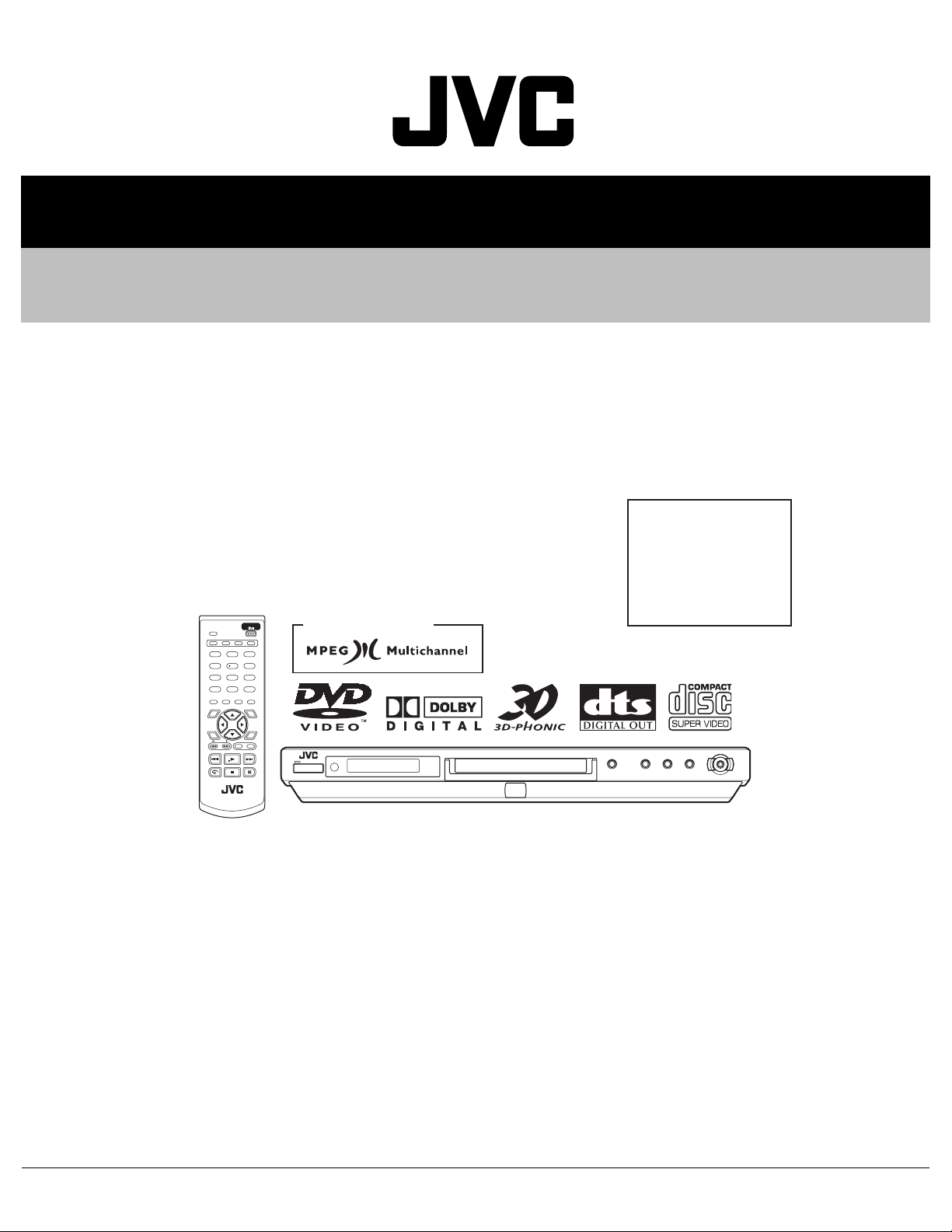
DVD VIDEO PLAYER
XA00220035
XV-N30BK[MK2],
XV-N33SL[MK2]
Area Suffix
J -------------------------- U.S.A.
C --------------------- Canada
B -------------------------- U.K.
E ------ Continental Europe
EN ------- Northern Europe
EV --------- Eastern Europe
DISPLAY
TITLE/
3D PHONIC
GROUP RETURN CANCEL
213
5
4
8
7
010 +10
ANGLE
SUB TITLE AUDIO ZOOM
TOP MENU MENU
CHOICE
SLOW
PREVIOUS SELECT
CLEAR
STANDBY/ON
6
9
ENTER
VFP ON SCREEN
NEXT
For only Europe
EE ---- Russian Federation
This illustration is XV-N30BK for U.S.A.
This service manual is a service manual of the model which
changes a part of specification of the above-mentioned model
which has already been put on the market.
Please refer to the following page for details.
TABLE OF CONTENTS
1 Important Safety Precautions . . . . . . . . . . . . . . . . . . . . . . . . . . . . . . . . . . . . . . . . . . . . . . . . . . . . . . . . . . . 1-4
2 Disassembly method . . . . . . . . . . . . . . . . . . . . . . . . . . . . . . . . . . . . . . . . . . . . . . . . . . . . . . . . . . . . . . . . . . 1-9
3 Adjustment. . . . . . . . . . . . . . . . . . . . . . . . . . . . . . . . . . . . . . . . . . . . . . . . . . . . . . . . . . . . . . . . . . . . . . . . . . 1-16
4 Description of major ICs. . . . . . . . . . . . . . . . . . . . . . . . . . . . . . . . . . . . . . . . . . . . . . . . . . . . . . . . . . . . . . . 1-25
COPYRIGHT © 2003 VICTOR COMPANY OF JAPAN, LIMITED.
No.XA002
2003/5
Page 2
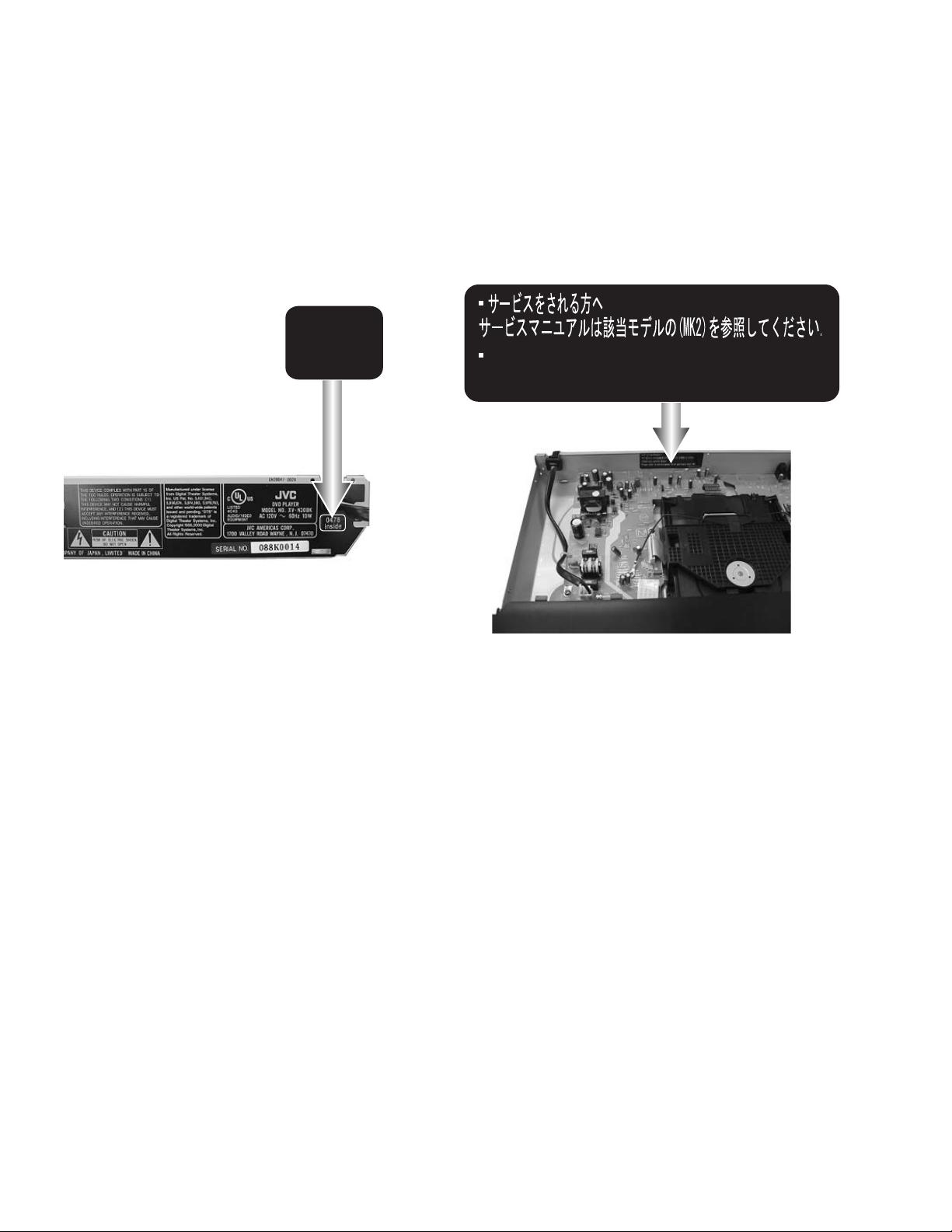
For this service manual
This service manual is a service manual of the model which changes a part of specification of the above-mentioned model
which has already been put on the market.
<When the label in figure is pasted in the main body>
The specification is different from what the label of the same model does not paste because of the specification improvement,
and refer to this service manual, please. Please already refer to the issued service manual when the label is not pasted.
* Please refer to this service manual for the model to which this label is pasted.
* Please refer to the service manual which has already been issued for the
model to which this label is not pasted.
(one that there is no description named [MK2] in cover of service manual. )
0478
The surface of a rear panel
inside
or
Used only service dealer
Please refer to service manual of an applicable model [MK2]
GN30080-001A
1-2 (No.XA002)
Page 3
SPECIFICATION
(For U.S.A.)
General
Readable discs DVD VIDEO, DVD-R (Video format), DVD-RW (Video format), +RW (Video format), SVCD, Video CD,
Audio CD (CD-DA), MP3 format, CD-R/RW (CD-DA, SVCD, Video CD, MP3 format)
Video format NTSC
Other
Power requirements AC 120 V, 60 Hz
Power consumption 10 W (POWER ON) 0.7 W (STANDBY mode)
Mass 2.1 kg (4.7 lbs)
Dimensions (W x H x D) 435mm x 53mm x 248.4mm (17-3/16 inch x 2-1/8 inc x 9-13/16 inch)
Video outputs
COMPONENT (pin jacks) Y Output: 1.0 Vp-p (75 ohm)
Pb/Pr Output: 0.7Vp-p (75 ohm)
VIDEO OUT (pin jack) 1.0 Vp-p (75 ohm)
S-VIDEO OUT (S jack) Y Output: 1.0 Vp-p (75 ohm)
C Output: 286 mVp-p (75 ohm)
Horizontal resolution 500 lines or more
Audio outputs
ANALOG OUT (pin jack) 2.0 Vrms (10 kohm)
DIGITAL OUT (COAXIAL) 0.5 Vp-p (75 ohm termination)
DIGITAL OUT (OPTICAL) -21 dBm to -15 dBm (peak)
Audio characteristics
Frequency response CD (sampling frequency 44.1 kHz):2 Hz to 20 kHz
DVD (sampling frequency 48 kHz):2 Hz to 22 kHz
(4 Hz to 20 kHz for DTS and Dolby Digital bitstream signals)
DVD (sampling frequency 96 kHz):2 Hz to 44 kHz
Dynamic range 16 bit: More than 98 dB
20 bit: More than 100 dB
24 bit: More than 100 dB
Wow and flutter Unmeasurable (less than + 0.002%)
Total harmonic distortion less than 0.006%
• Specifications and appearance are subject to change without prior notice.
• Manufactured under license from Dolby Laboratories. "Dolby" and the double-D symbol are trademarkes of Dolby Laboratories.
• Manufactured under license from Digital Theater Systems, Inc. "DTS" and "DTS Digital Surround" are registered trademarks of Digital Theater Systems, Inc.
(No.XA002)1-3
Page 4
SECTION 1
Important Safety Precautions
1.1 Safety Precautions
(1) This design of this product contains special hardware and
many circuits and components specially for safety purposes. For continued protection, no changes should be made
to the original design unless authorized in writing by the
manufacturer. Replacement parts must be identical to
those used in the original circuits. Services should be performed by qualified personnel only.
(2) Alterations of the design or circuitry of the product should
not be made. Any design alterations of the product should
not be made. Any design alterations or additions will void
the manufacturers warranty and will further relieve the
manufacture of responsibility for personal injury or property
damage resulting therefrom.
(3) Many electrical and mechanical parts in the products have
special safety-related characteristics. These characteristics are often not evident from visual inspection nor can the
protection afforded by them necessarily be obtained by using replacement components rated for higher voltage, wattage, etc. Replacement parts which have these special
safety characteristics are identified in the Parts List of Service Manual. Electrical components having such features
are identified by shading on the schematics and by ( ) on
the Parts List in the Service Manual. The use of a substitute
replacement which does not have the same safety characteristics as the recommended replacement parts shown in
the Parts List of Service Manual may create shock, fire, or
other hazards.
(4) The leads in the products are routed and dressed with ties,
clamps, tubings, barriers and the like to be separated from
live parts, high temperature parts, moving parts and/or
sharp edges for the prevention of electric shock and fire
hazard. When service is required, the original lead routing
and dress should be observed, and it should be confirmed
that they have been returned to normal, after reassembling.
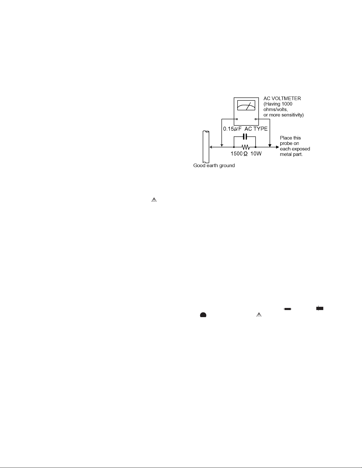
(5) Leakage shock hazard testing)
After reassembling the product, always perform an isolation check on the exposed metal parts of the product (antenna terminals, knobs, metal cabinet, screw heads,
headphone jack, control shafts, etc.) to be sure the product
is safe to operate without danger of electrical shock.Do not
use a line isolation transformer during this check.
• Plug the AC line cord directly into the AC outlet. Using a
"Leakage Current Tester", measure the leakage current
from each exposed metal parts of the cabinet, particularly any exposed metal part having a return path to the
chassis, to a known good earth ground. Any leakage current must not exceed 0.5mA AC (r.m.s.).
• Alternate check method
Plug the AC line cord directly into the AC outlet. Use an
AC voltmeter having, 1,000 ohms per volt or more sensitivity in the following manner. Connect a 1,500 ohm 10W
resistor paralleled by a 0.15 F AC-type capacitor between an exposed metal part and a known good earth
ground.
Measure the AC voltage across the resistor with the AC
voltmeter.
Move the resistor connection to each exposed metal
part, particularly any exposed metal part having a return
path to the chassis, and measure the AC voltage across
the resistor. Now, reverse the plug in the AC outlet and
repeat each measurement. Voltage measured any must
not exceed 0.75 V AC (r.m.s.). This corresponds to 0.5
mA AC (r.m.s.).
1.2 Warning
(1) This equipment has been designed and manufactured to
meet international safety standards.
(2) It is the legal responsibility of the repairer to ensure that
these safety standards are maintained.
(3) Repairs must be made in accordance with the relevant
safety standards.
(4) It is essential that safety critical components are replaced
by approved parts.
(5) If mains voltage selector is provided, check setting for local
voltage.
1.3 Caution
Burrs formed during molding may be left over on some parts
of the chassis.
Therefore, pay attention to such burrs in the case of preforming repair of this system.
1.4 Critical parts for safety
In regard with component parts appearing on the silk-screen
printed side (parts side) of the PWB diagrams, the parts that are
printed over with black such as the resistor ( ), diode ( )
and ICP ( ) or identified by the " " mark nearby are critical for
safety. When replacing them, be sure to use the parts of the
same type and rating as specified by the manufacturer. (Except
the JC version)
1-4 (No.XA002)
Page 5
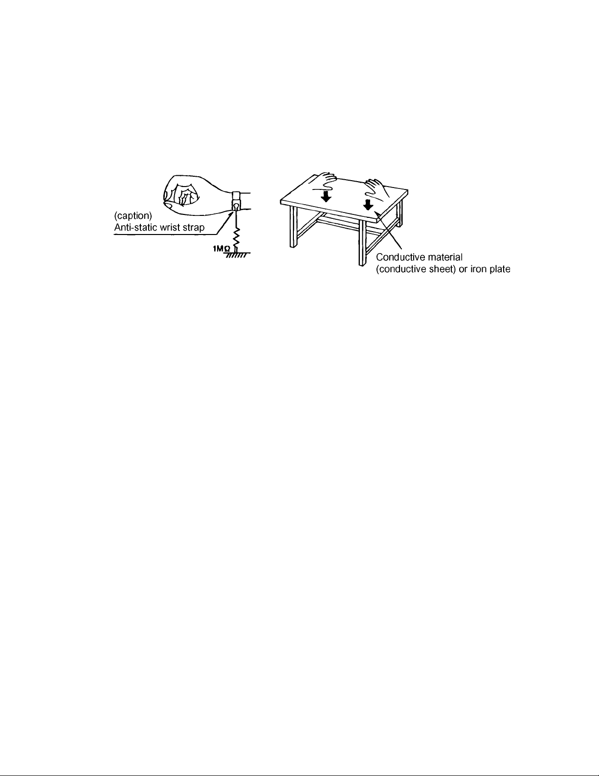
1.5 Preventing static electricity
Electrostatic discharge (ESD), which occurs when static electricity stored in the body, fabric, etc. is discharged, can destroy the laser
diode in the traverse unit (optical pickup). Take care to prevent this when performing repairs.
1.5.1 Grounding to prevent damage by static electricity
Static electricity in the work area can destroy the optical pickup (laser diode) in devices such as DVD players.
Be careful to use proper grounding in the area where repairs are being performed.
(1) Ground the workbench
Ground the workbench by laying conductive material (such as a conductive sheet) or an iron plate over it before placing the
traverse unit (optical pickup) on it.
(2) Ground yourself
Use an anti-static wrist strap to release any static electricity built up in your body.
(3) Handling the optical pickup
• In order to maintain quality during transport and before installation, both sides of the laser diode on the replacement optical
pickup are shorted. After replacement, return the shorted parts to their original condition.
(Refer to the text.)
• Do not use a tester to check the condition of the laser diode in the optical pickup. The tester's internal power source can easily
destroy the laser diode.
1.6 Handling the traverse unit (optical pickup)
(1) Do not subject the traverse unit (optical pickup) to strong shocks, as it is a sensitive, complex unit.
(2) Cut off the shorted part of the flexible cable using nippers, etc. after replacing the optical pickup. For specific details, refer to the
replacement procedure in the text. Remove the anti-static pin when replacing the traverse unit. Be careful not to take too long
a time when attaching it to the connector.
(3) Handle the flexible cable carefully as it may break when subjected to strong force.
(4) I t is not possible to adjust the semi-fixed resistor that adjusts the laser power. Do not turn it.
1.7 Precautions of the safe use of battery (Only XV-N30BK for U.S.A.)
• Store the battery in a place where children cannot reach.If a child accidentally swallows the battery, consult a doctorimmediately.
• Do not recharge, short, disassemble or heat the battery or dispose of it in a fire.
Doing any of these things may cause the battery to give off heat, crack, or start a fire.
• Do not leave the battery with other metallic materials.Doing this may cause the battery to give off heat, crack, or start a fire.
• When throwing away or saving the battery, wrap it in tape and insulate; otherwise, the battery may start to give off heat, crack, or
start a fire.
• Do not poke the battery with tweezers or similar tools.Doing this may cause the battery to give off heat, crack, or start a fire.
• Dispose of batteries in the proper manner, according to federal, state, and local regulations.
(No.XA002)1-5
Page 6
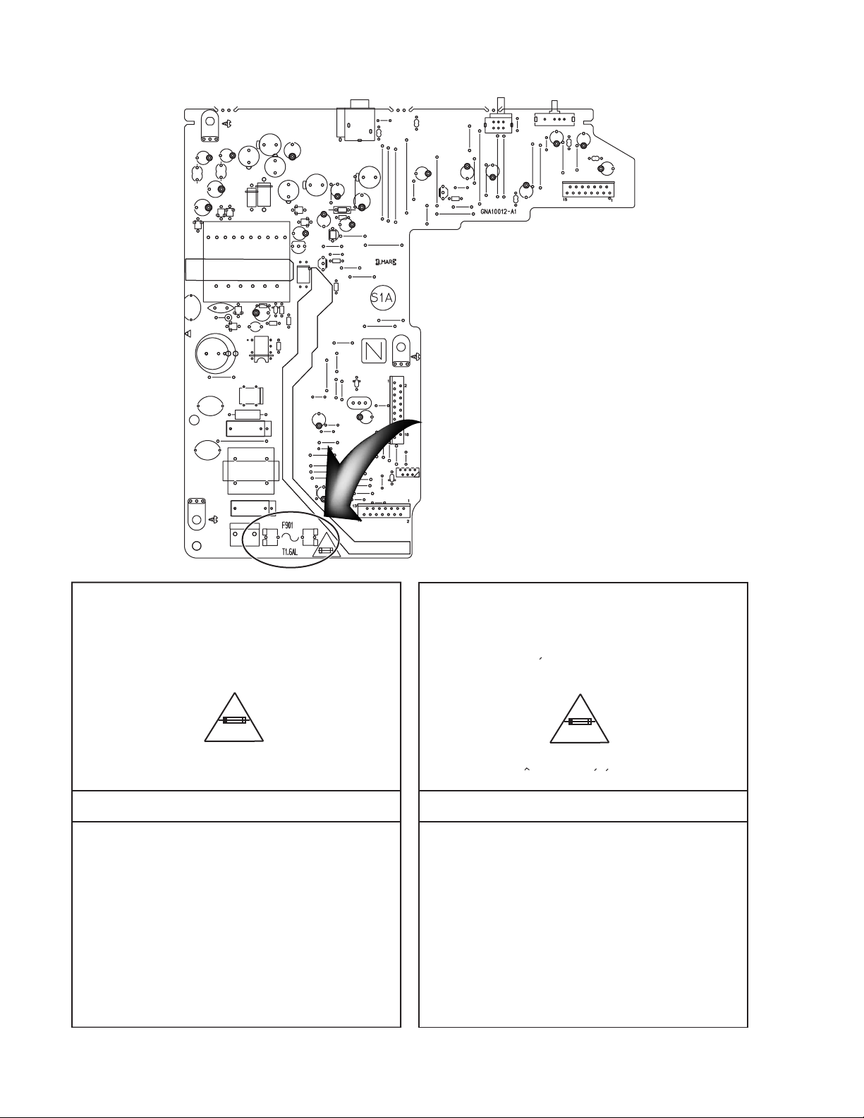
1.8 Importance admistering point on the safety
J702
EP953
C966
C965
L954
L953
C963
D957
D956
T901
C908
R901
C906
C907
B234
R910
C904
C918
C905
L901
C902
EP951
P901
L955
C988
C967
C964
D954
D903
D901
B631
C958
D953
D955
R912
D902
C914
R915
C913
IC901
FC901
L951
C952
D951
R903
D904
R906
C955
B141
D952
PC901
R913
R954
C950
C970
CP951
B137
IC952
B34
Q951
R953
R951
B116
B135
B303
B133
B134
B37
C701
B38
B39
B132
B40
B202
B231
B233
B105
C808
C802
B45
FC902
B4
L710
L709
L952
B331
C953
R969
C951
B236
B136
B271
B347
D701
X701
C706
B201
B142
B143
B170
B203
B102
B16
C959
B140
B852
B871
B874
B872
B166
B403
B237
EP952
CN904
B36
B103
B101
B171
B44
P704
B2
D702
B41
CN901
S901
B273
B873
C973
B601
Q953
B32
R966
B272
B139
B138
,,
B17
B772
B771
C957
B332
B532
C977
L959
S902
C975
C976
L957
B15
B533
L956
B276
B333
C974
CN902
Full Fuse Replacement Marking
Graphic symbol mark
(This symbol means fast blow type fuse.)
should be read as follows ;
FUSE CAUTION
FOR CONTINUED PROTECTION AGAINST RISK
OF FIRE, REPLACE ONLY WITH SAME TYPE
AND RATING OF FUSES ;
F901 : 1.6 A / 125 V F901 : 1.6 A / 125 V
Marquage Pour Le Remplacement
Complet De Fusible
Le symbole graphique (Ce symbole signifie
fusible de type a fusion rapide.)
doit etre interprete comme suit ;
PRECAUTIONS SUR LES FUSIBLES
POUR UNE PROTECTION CONTINUE CONTRE
DES RISQUES D'INCENDIE, REMPLACER
SEULEMENT PAR UN FUSIBLE DU MEME TYPE ;
1-6 (No.XA002)
Page 7
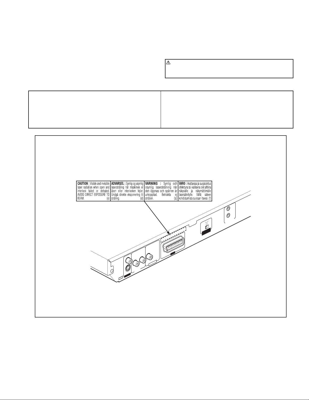
1.9 Important for laser products
(1) CLASS 1 LASER PRODUCT
(2) DANGER : Invisible laser radiation when open and inter
lock failed or defeated. Avoid direct exposure to beam.
(3) CAUTION : There are no serviceable parts inside the
Laser Unit. Do not disassemble the Laser Unit. Replace the
complete Laser Unit if it malfunctions.
(4) CAUTION : The compact disc player uses invisible laser
radiation and is equipped with safety switches which
prevent emission of radiation when the drawer is open and
the safety interlocks have failed or are de feated.
It is dangerous to defeat the safety switches.
VARNING
Osynlig laserstrålning är denna del är öppnad och spårren är
urkopplad. Betrakta ej strålen.
VARO
Avattaessa ja suojalukitus ohitettaessa olet alttiina näkymättömälle lasersäteilylle. Älä katso säteeseen.
ADVARSEL
Usynlig laserstråling ved åbning, når sikkerhedsafbrydere er
ude af funktion. Undgå udsasttelse for stråling.
ADVARSEL
Usynlig laserstråling ved åpning, når sikkerhetsbryteren er avslott. unngå utsettelse for stråling.
REPRODUCTION AND POSITION OF LABEL and PRINT
WARNING LABEL and PRINT
(5) CAUTION : If safety switches malfunction, the laser is able
to function.
(6) CAUTION : Use of controls, adjustments or performance of
procedures other than those specified herein may result in
hazardous radiation exposure.
CAUTION
Please use enough caution not to see the beam directly
or touch it in case of anadjustment or operation check.
The inside of a rear panel
M
A
PCM/STRE
COAXIAL
LEFT
VIDEO
S-VIDEO
ID
V
EO O
RIGHT
U
O
IO
D
AU
T
U
UT
O
AL
IT
DIG
T
/C
Y
.
P
COM
B
G
/R
SIGNAL
OR
VIDEO
SELECT
T
U
O
V
A
COMPU LINK
AV
(No.XA002)1-7
Page 8
1.10 Precautions for Service
1.10.1 Handling of Traverse Unit and Laser Pickup
(1) Do not touch any peripheral element of the pickup or the actuator.
(2) The traverse unit and the pickup are precision devices and therefore must not be subjected to strong shock.
(3) Do not use a tester to examine the laser diode. (The diode can easily be destroyed by the internal power supply of the tester.)
(4) To replace the traverse unit, pull out the metal short pin for protection from charging.
(5) When replacing the pickup, after mounting a new pickup, remove the solder on the short land which is provided at the center of
the flexible wire to open the circuit.
(6) Half-fixed resistors for laser power adjustment are adjusted in pairs at shipment to match the characteristics of the optical block.
Do not change the setting of these half-fixed resistors for laser power adjustment.
1.10.2 Destruction of Traverse Unit and Laser Pickup by Static Electricity
Laser diodes are easily destroyed by static electricity charged on clothingor the human body. Before repairing peripheral elements of
the traverse unit or pickup, be sure to take the following electrostatic protection:
(1) Wear an antistatic wrist wrap.
(2) With a conductive sheet or a steel plate on the workbench on which the traverse unit or the pick up is to be repaired, ground the
sheet or the plate.
(3) It solders to two short circuit sections on the substrate of a pick-up.
(4) After removing the flexible wire from the connector (CN101), short-circuit the flexible wire by the metal clip.
(5) Short-circuit the laser diode by soldering the land which is provided at the center of the flexible wire for the pickup.
After completing the repair, remove the solder to open the circuit.
Pick-up
Short circuit
* Please refer to the disassembly method for details.
CN101
Servo control board
1-8 (No.XA002)
Page 9
SECTION 2
TOP COVER
r
Push
Disassembly method
There is a part different from the photograph according to the model and the destination though explains this disassembly method
by using XV-N30BK for U.S.A.
2.1 Main body section
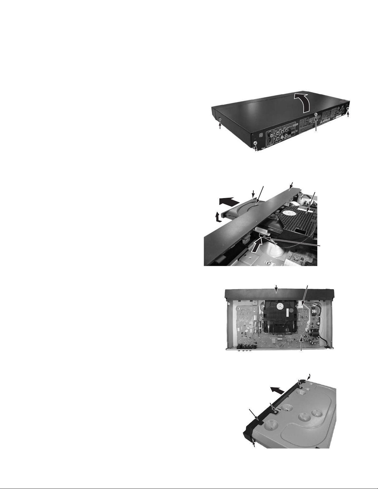
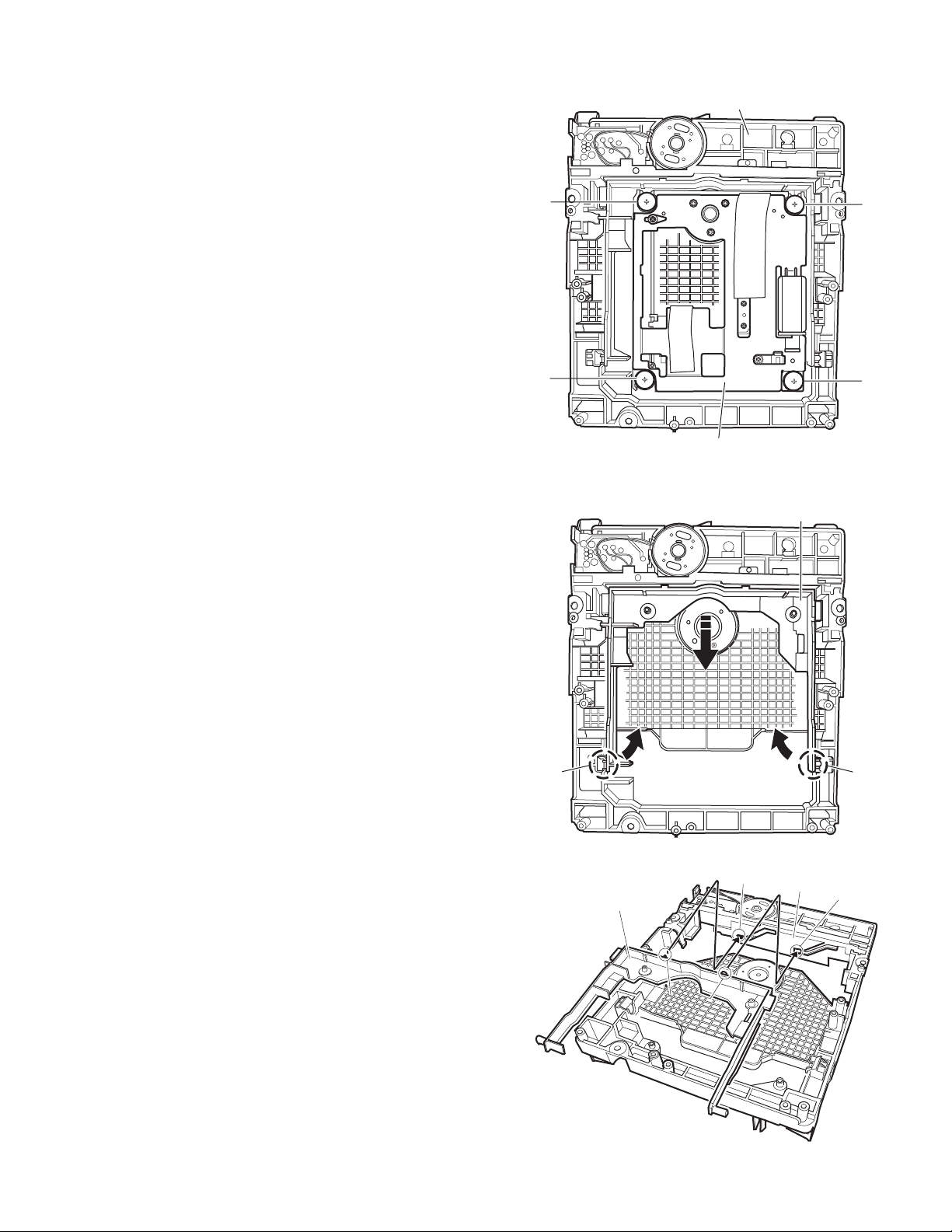
2.1.1 Removing the top cover (See Figure 1)
(1) Remove the two screws A attaching the top cover on both
sides of the main body.
(2) Remove the three screws B attaching the top cover on the
back of the main body.
(3) Raise the both sides and lower part of the rear of the top
cover, with opening them slightly in an outward direction.
And the top cover will be removed.
2.1.2 Removing the front panel assembly (See Figure 2, Figure 3, Figure 4)
• Prior to performing the following procedure, remove the top
cover.
• There is no need to remove the mechanism assembly.
(1) Insert a kind of screwdriver in a hole located in the right
side of mechanism assembly, and push a lever until it cannot be inserted any further.
(2) And then, a tray will come out. Remove the tray in an upper
direction, with slightly opening the lower part of fitting in an
outward direction.
(3) Disconnect the card wire from connector CN901 on the
power supply board.
(4) Hook a and b are removed respectively, and the front panel
assembly is removed.
A
x
2
Fitting
B
Push
TOP COVER
TOP COVER
Fig.1
Tray
B
Front panel assembly
Mechanism assembly
Hole and leve
B
Fig.2
Front panel assembly
Power supply board
Fig.3
Hook b
Front panel
assembly
Hook b
Hook a
Fig.4
CN901
Hook a
(No.XA002)1-9
Page 10
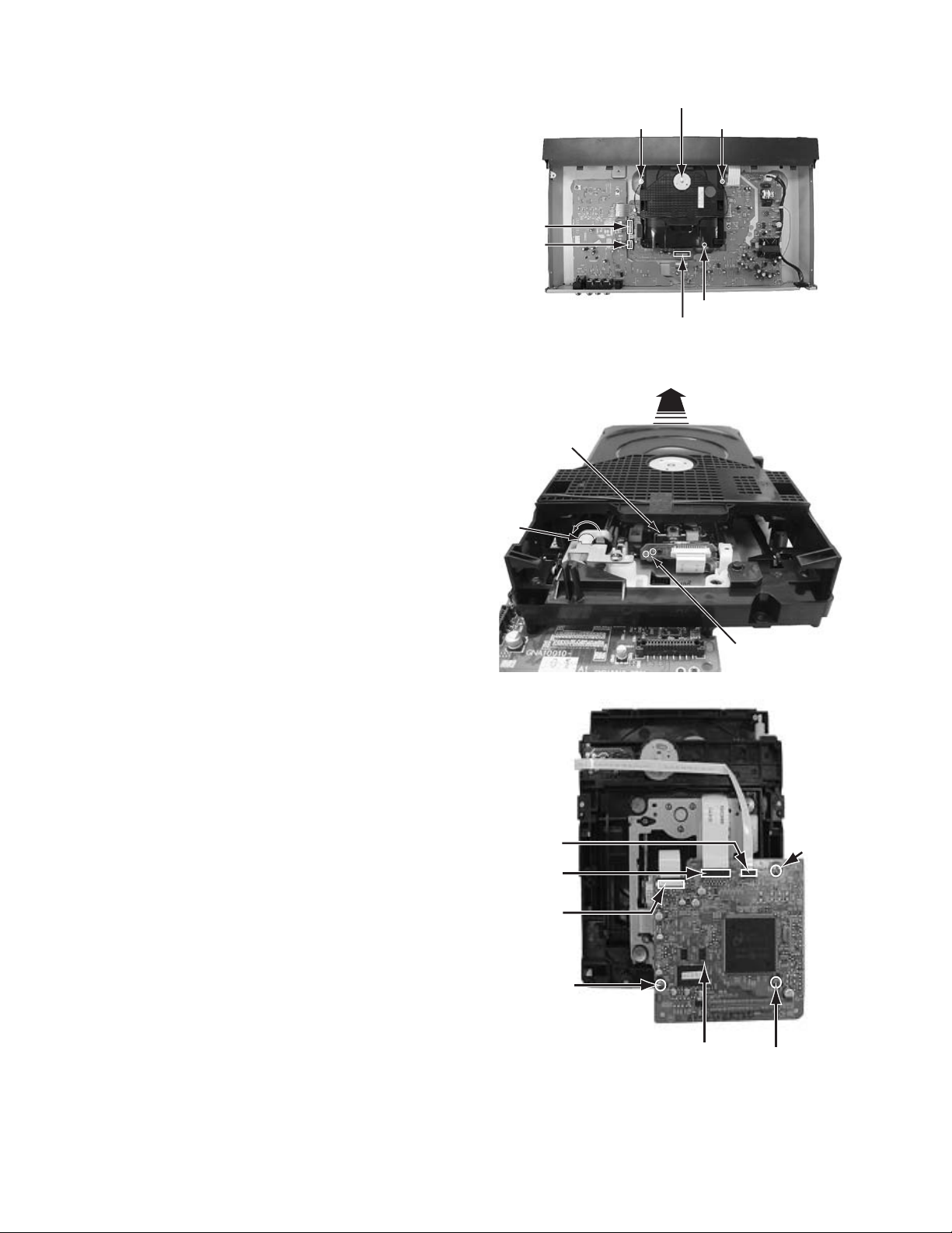
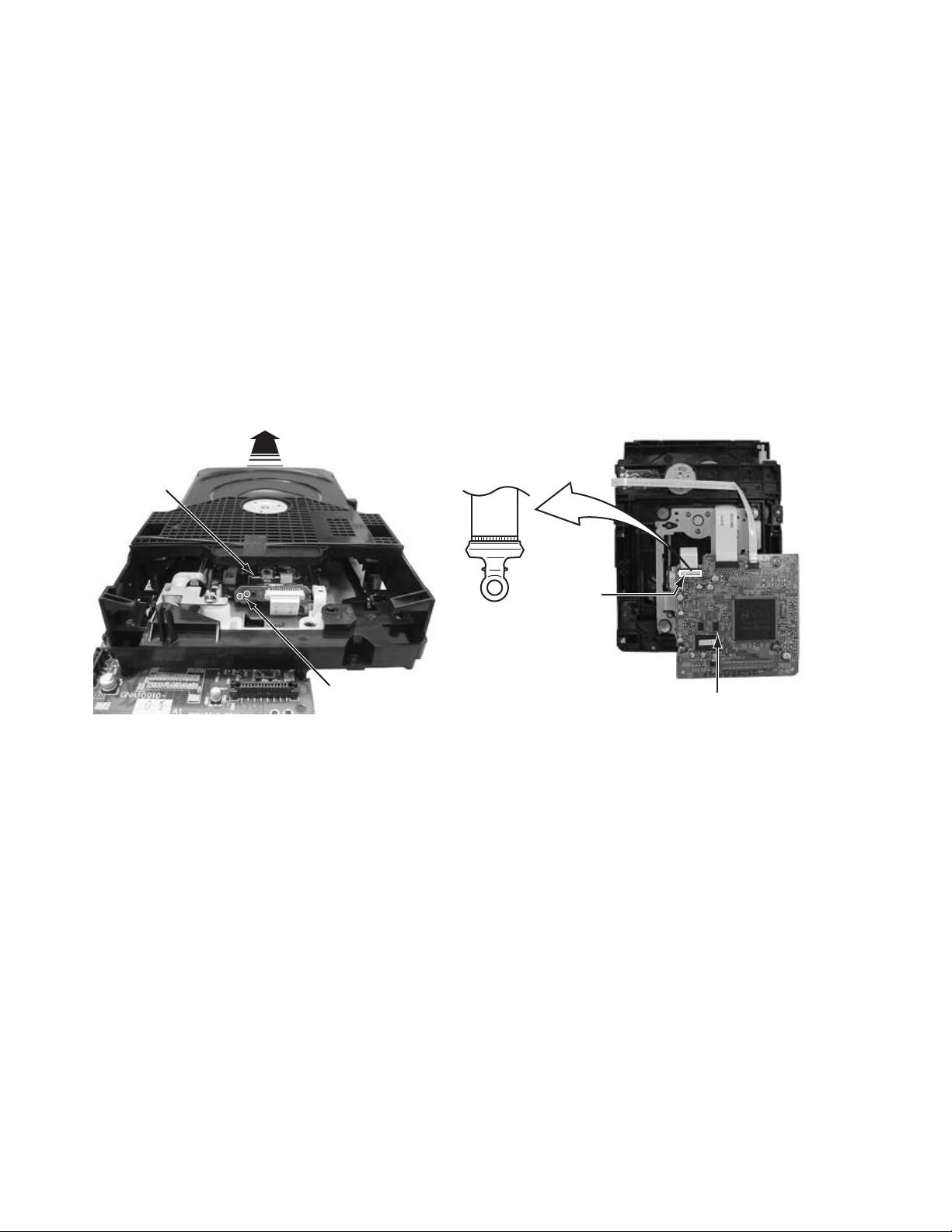
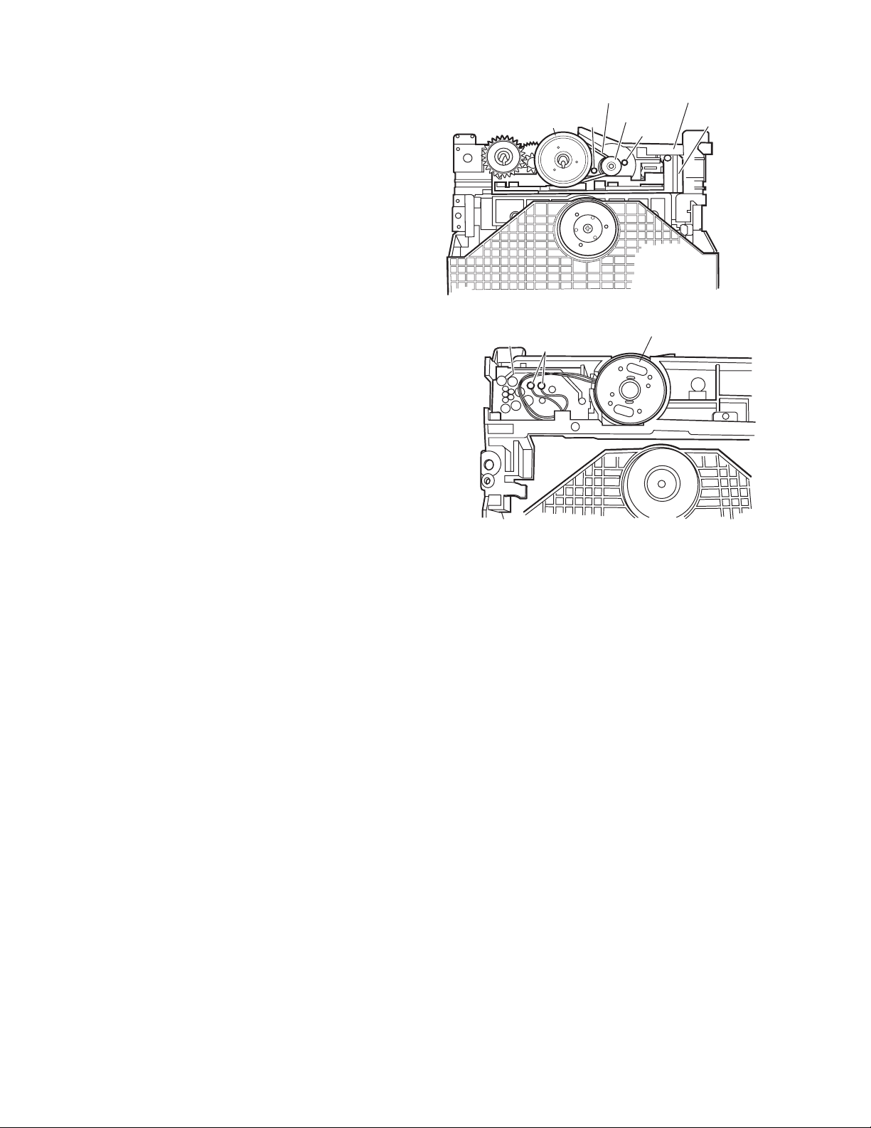
2.1.3 Removing the mechanism assembly (See Figure 2, Figure 5)
• Prior to performing the following procedure, remove the top
cover.
• There is no need to remove the front panel assembly.
(1) Insert a kind of screwdriver in a hole located in the right
side of mechanism assembly, and push a lever until it cannot be inserted any further.
(2) And then, a tray will come out. Remove the tray in an upper
direction, with slightly opening the lower part of fitting in an
outward direction.
(3) Remove the three screws C attaching the mechanism as-
sembly.
(4) Disconnect the wire from connector CN501,CN502,CN503
on the servo control board respectively.
(5) Remove the mechanism assembly by lifting the rear part of
the mechanism assembly.
2.1.4 Removing the servo control board (See Figure 6, Figure 7)
• Prior to performing the following procedure, remove the mechanism assembly.
(1) A tray is made to slide ahead.
(2) A gear 1 is turned counterclockwise. Then, a pick-up unit
moves back.
(3) It solders to two c sections on the pick-up unit.
(4) Remove the three screws D attaching the servo control
board.
(5) Disconnect the card wire from connector CN201,CN202 on
the servo control board.
(6) Disconnect the flexible wire from connector CN101 on the
servo control board from pick-up unit.
ATTENTION:
Please extract the wire after short-circuited of two places
on the wire in part c with solder. Please remove the solder two places of part c after connecting the wire with
CN101 when reassembling.
CAUTION:
Be sure to solder the short land sections “c” on the pickup unit before disconnecting the card wire from connector CN101 on the DVD servo control board.
If the card wire is disconnected without attaching solder,
the pick-up unit may be destroyed by static electricity.
CN502
CN503
Gear1
Pick-up
Mechanism assembly
C
CN501
Fig.5
Fig.6
C
C
Part c
1-10 (No.XA002)
CN202
CN201
CN101
D
Servo control board
Fig.7
D
D
Page 11
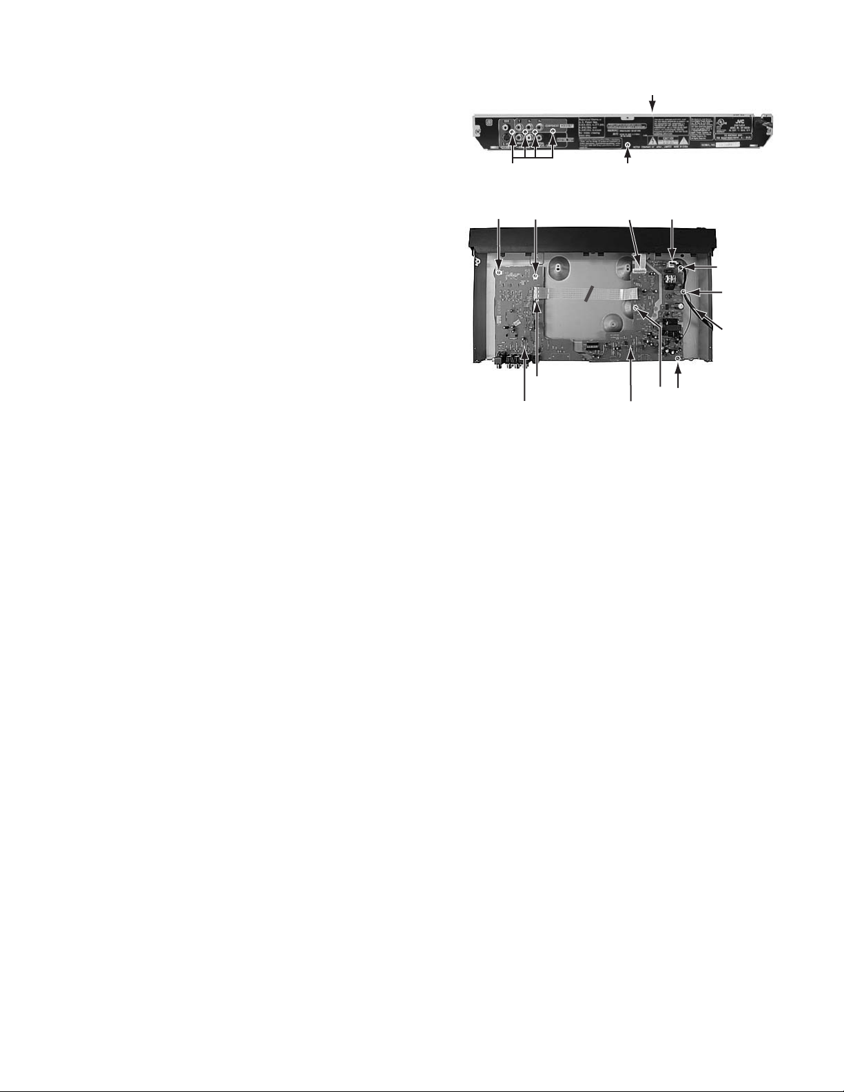
2.1.5 Removing the rear panel (See Figure 8, Figure 9)
• Prior to performing the following procedure, remove the top
cover.
(1) Remove the five screws E attaching the rear panel.
(2) Disconnect the power cord from connector P901 on the
power supply board
(3) Remove tie band.
Rear panel
E
E
Fig.8
G G
CN702
2.1.6 Removing the output terminal board and power supply board. (See Figure 9)
• Prior to performing the following procedure, remove the top
cover/mechanism assembly/rear panel.
(1) Remove the two screws G attaching the output terminal
board.
(2) Disconnect the card wire from connector CN702 on the
output terminal board.
(3) Remove the three screws H attaching the power supply
board.
(4) Disconnect the card wire from connector CN901 on the
power supply board.
CN901 P901
H
Power supply boardOutput terminal board
Fig.9
H
Tie band
Power cord
H
(No.XA002)1-11
Page 12
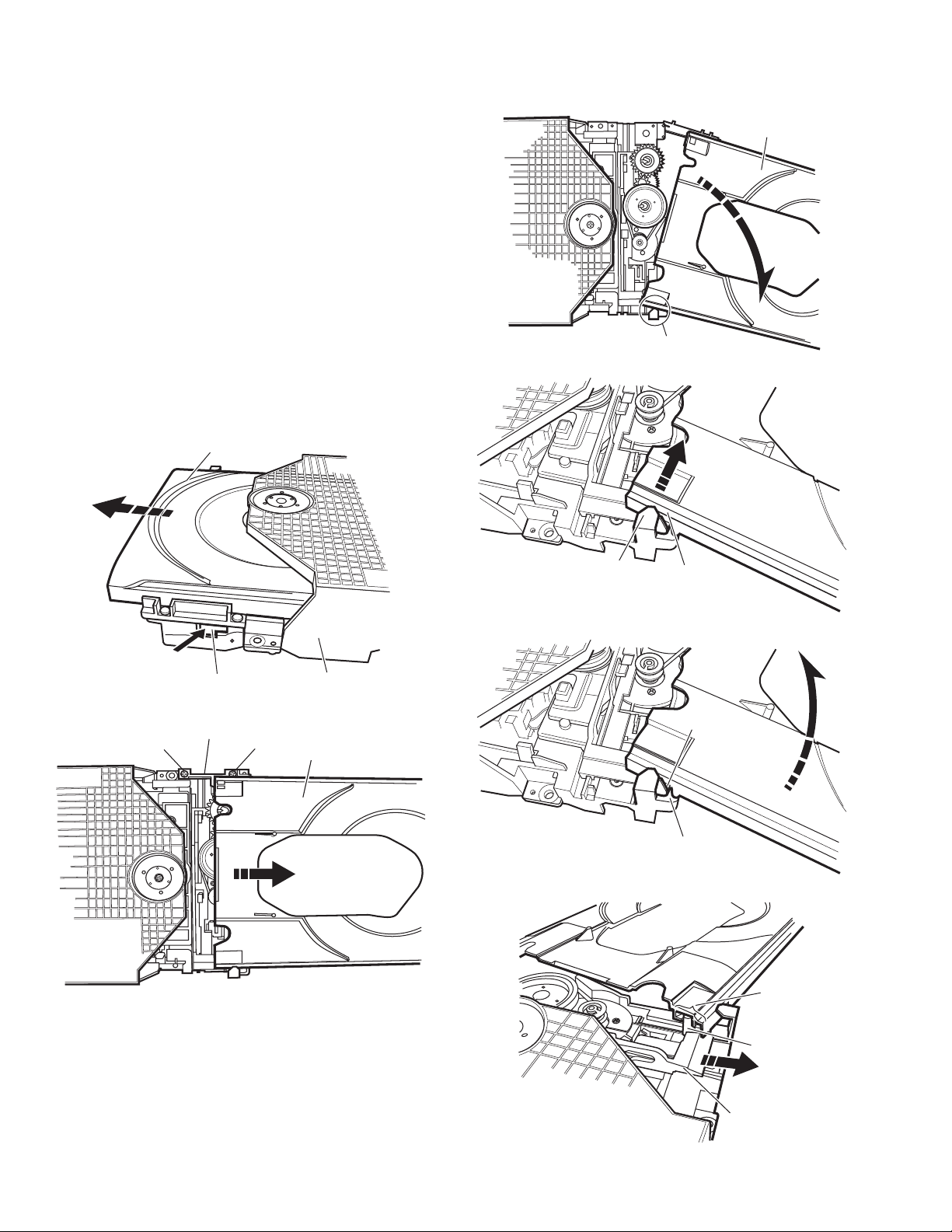
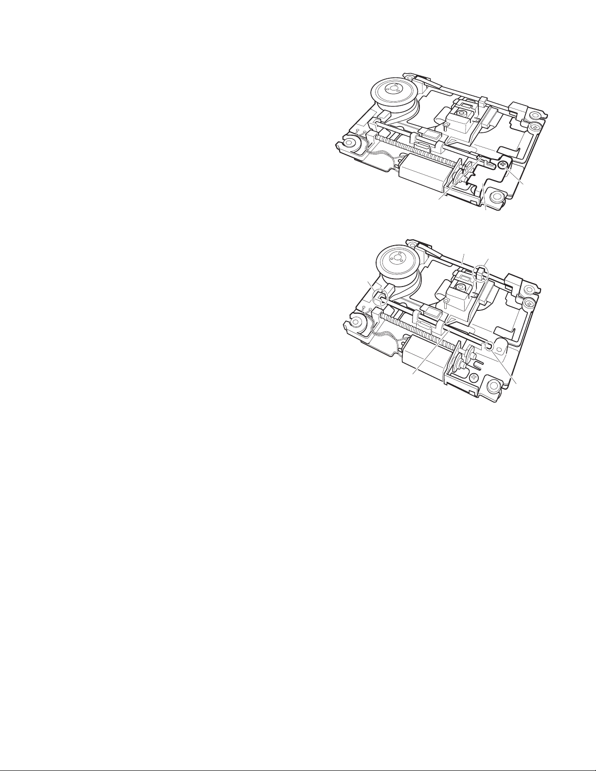
2.2 Loading mechanism assembly
Projection of the tray
2.2.1 Removing the tray (See Figure 1, Figure 2, Figure 3, Figure 4, Figure 5, Figure 6)
(1) Push a of the slide cam on the hole in the right side of the
loading base by using a driver until it stops. (See Figure 1.)
(2) The tray comes out. Pull the tray in a front direction until it
stops.
(3) Remove the two screws A attaching the slide bracket. (See
Figure 2.)
(4) Tilt the tray in a direction of the arrow around the point in
the left rear part of the tray. (See Figure 3.)
(5) The rail of the tray is removed from b of the loading base.
Then, remove the tray upward. (See Figure 4.)
Attaching the tray:
Engage c of the loading base to the projection of the tray while
tilting the tray to the left. Turn the tray in a direction of the arrow, and attach the slide bracket. (See Figure 5.)
Note:
Prior to the procedure above, move the slide cam in a direction
of the arrow so that d of the slide cam can be inserted in e of
the tray. (See Figure 6.)
Tray
The point in the left rear part
Tray
Fig.3
Push
Slide cam part a
Slide bracket
A
Fig.1
Fig.2
A
Loading base
Tray
Loading base part b
Rail of the tray
Fig.4
Projection of the tray
Loading base part c
Fig.5
Part e
1-12 (No.XA002)
Part d
Slide cam
Fig.6
Page 13
2.2.2 Removing the traverse mechanism assembly (See Figure 7)
f
Shaft
Reverse the loading mechanism assembly. Remove the four
screws B attaching the traverse mechanism assembly. Remove
the traverse mechanism assembly upward.
Loading mechanism assembly
2.2.3 Removing the elevator (See Figure 8 and Figure 9)
• Prior to the following procedure, remove the traverse mechanism assembly.
(1) Remove the two arms of the elevator from the two parts f
by moving the arms in a direction of the arrow.
(2) Pull out the elevator in a rear direction.
Attaching the elevator:
Engage the two holes g to the two shafts on the front part of
the elevator. And then, attach the elevator.
B
B
B
B
Traverse mechanism assembly
Fig.7
Elevator
Part f
Fig.8
g
Slide cam
Elevator
Shaft
Fig.9
(No.XA002)1-13
Part
g
Page 14
2.2.4 Removing the loading motor (See Figure 10 and Figure 11)
• Prior to the following procedure, remove the tray, the traverse
mechanism assembly, and the elevator.
(1) Remove the belt from the pulley.
(2) Remove two screws C attaching the loading motor.
(3) Remove two solders h on the switch board.
Pulley
Belt
C
Fig.10
Pulley
C
Loading base
Slide cam
Switch board
Loading motor
Part h
Fig.11
1-14 (No.XA002)
Page 15
2.3 Traverse mechanism assembly
2.3.1 Removing the pickup (See Figure 12, Figure 13)
• Prior to the following procedure, remove the traverse mechanism assembly.
(1) Remove one screw D attaching the plate.
(2) Remove the plate and the leaf spring.
(3) Lift i of the shaft 1, and pull out the shaft 1 from j.
(4) Remove k of the pickup from the shaft 2.
Attaching the pickup:
(1) Engage k of the pickup to the shaft 2.
(2) Insert the shaft 1 in j, and attach the shaft 1 to i.
(3) Attach the leaf spring, and then attach the plate. Fix the
leaf spring and the plate by using the screw D.
D
Leaf spring
Plate
Fig.12
Part j
Shaft 2
Part k
Shaft 1
Part i
Fig.13
(No.XA002)1-15
Page 16

SECTION 3
Adjustment
3.1 Test mode setting method
(1) Unplug the power plug.
(2) Insert power plug into outlet while pressing both "PLAY" key and "STOP" key of the main body.
(3) The FL display shows " 0", and the main body turns to test mode. " " means the destination, and "0" means parameter adjust-
ment status.
(4) To release test mode, press "POWER" key of the main body.
NOTE:
Each pressing of "CHOICE" key of the remote controller in test mode changes the mode as follows.
0 ------------------------------
_ ----------------------
Becames test mode
Version of firmware
FL Display becames all lighting
CK --------------------------------
EP -------------------------------
3.2 Method of displaying version of firmware
(1) Set the main body at test mode.
(2) Press "CHOICE" key of the remote controller once. Then, version number and alphabetical letter of the system controller and
the back end are displayed in the FL display as follows:
Check mode
Not used
FL Display (Example)
19_16
System controller
3.3 Initialization method
Please initialize according to the following procedures in the following case:
• Just after you upgrade the firmware.
• After you confirm the symptoms that a customer points out. First Initialize, and then confirm whether the symptoms are improved or
not.
• After servicing, before returning the main body to a customer. (Initialized main body should be returned to a customer.)
(1) Set the main body at test mode.
(2) Press "PAUSE" key of the main body.
(3) When initialization is completed, the FL display changes from " 0" to " 00".(The left "0" of "00" is not always "0". It shows pa-
rameter adjustment status.)
STANDBY/ON
DISPLAY
TITLE/
3D PHONIC
GROUP RETURN CANCEL
213
5
6
4
8
9
7
010 +10
ANGLE
SUB TITLE AUDIO ZOOM
TOP MENU MENU
CHOICE
SLOW
VFP ON SCREEN
PREVIOUS SELECT
CLEAR
CHOICE key
ENTER
(switch of mode)
NEXT
POWER key
FL Display
Back end
PLAY key
(for test mode)
STOP key
(for test mode)
1-16 (No.XA002)
PAUSE key
(for initialize)
Page 17

3.4 All-initialization method
Please perform all-initialization according to the following procedures in the following case:
• Just after you exchange the pick-up.
• Just after you exchange the spindle motor.
• Just after you exchange the traverse mechanism base.
NOTE:
Please perform all-initialization when you exchange the parts above and also when you remove the parts above.
• Just after the flap adjustment of the pick-up guide shaft
(1) Set the main body at test mode.
(2) Press and hold "BACKWARD SKIP" key of the main body for more than 2 seconds.
(3) When all-initialization is completed, the FL display changes from " 0" to " 33".
NOTE:
After all-initialization, be sure to perform optimization adjustment of Front End parameter.
3.5 Optimization adjustment of Front End parameter
Adjustment to optimize Front End parameter must be performed in each mechanism assembly of this model for high-speed starting.Please perform optimization according to the following procedures just after all-initialization is completed and when FL display
shows anything except " 0" (For example when FL display shows " 1", " 2", and " 3") at test mode.
(1) Press "POWER" key of the main body to turn the main body on (not to set the main body at test mode).
(2) Insert the test disc VT-501 or commercial dual-layer DVD software.
(3) Remove the disc when the FL display changes from "READ" to disc information.
(4) Perform the same procedures as in (2) and (3) above by using the test disc CTS-1000 or commercial CD-DA software.
(5) Set the main body at test mode, and check that the FL display shows " 0".
NOTE:
Status of this adjustment can be judged by the number displayed at test mode as follows:
DVD adjustment CD adjustment FL display at test mode
Adjusted Adjusted 0
Not adjusted Adjusted 1
Adjusted Not adjusted 2
Not adjusted Not adjusted 3
NOTE:
As for a disc used for adjustment,
• Disc should be mounted. ("Mounting" means to display "READ" after the disc is inserted and then display the disc information.) Disc need not be played.
• If you do not have test disc either VT-501 (DVD) or CTS-1000 (CD-DA), use a commercial disc (for DVD, dual-layer software) after seeing and checking that the disc is neither curved nor foreseen that it may shake at the time of playback.If you
use a disc with bad features, starting time may be slow or disc may not be read.
STANDBY/ON
DISPLAY
TITLE/
3D PHONIC
GROUP RETURN CANCEL
213
5
4
8
7
010 +10
ANGLE
SUB TITLE AUDIO ZOOM
TOP MENU MENU
CHOICE
SLOW
VFP ON SCREEN
PREVIOUS SELECT
CLEAR
6
9
STOP key
ENTER
POWER key
NEXT
FL Display
(for test mode)
BACKWARD SKIP key
(for All initialize : It pushes 2 seconds or more.)
PLAY key
(for test mode)
(No.XA002)1-17
Page 18

3.6 Display of current value of laser
(1) Set the main body at test mode.
(2) Press "CHOICE" key of the remote controller three times. Then, FL display is displayed "CK".
(3) The laser current value can be switched between the value of CD and that of DVD by pressing the following key of the remote
controller.
FL Display (Example)
2530
The number shown in the FL display shows mA of current value of laser.
The first two numbers ("25" in "2530") shows current value of laser at the time of adjustment after the latest all-initialization, 25mA
in this example.
The last two numbers ("30" in "2530") shows the present current value of laser, 30mA in this example.
The first two numbers ("25" in "2530") usually shows current value of laser at the time of shipment, so you can see how the product has been deteriorated by comparing the first two numbers ("25" in "2530") and the last two numbers ("30" in "2530").
CD and DVD:
The laser current value of 80 mA or less is normal.The laser current value of over 81 mA is n ot normal. Laser diode of the
pickup has been deteriorated.
To return to test mode, press "STOP" key of the main body.
3.7 Flap adjustment of the pick-up guide shaft
Please perform flap adjustment of the pick-up guide shaft in the following case:
• Just after you exchange the pick-up.
• Just after you exchange the spindle motor.
• Just after you exchange the traverse mechanism base.
NOTE:
Please perform flap adjustment of the pick-up guide shaft when you exchange the parts above and also when you remove the
parts above.
• When the reading accuracy of the signal is bad (There is a b lock noise in the screen, Screen stops in the outer circumference of a
disc, etc.)
4 key (laser of CD)
5 key (laser of DVD)
STANDBY/ON
DISPLAY
TITLE/
GROUP RETURN CANCEL
3D PHONIC
213
5
6
4
7
SUB TITLE AUDIO ZOOM
ANGLE
TOP MENU MENU
CHOICE
SLOW
PREVIOUS SELECT
CLEAR
6 key
8
9
(display of jitter value)
010 +10
CHOICE key
ENTER
(switch of mode)
VFP ON SCREEN
NEXT
POWER key
Remote controller "4" key --- Laser of CD
Remote controller "5" key --- Laser of DVD
(for test mode and jitter value)
STOP key
FL Display
(for test mode)
PLAY key
1-18 (No.XA002)
Page 19

3.7.1 Tool for adjustment
*Stud: One set (four studs), Part number: JIGXVS40 (Note: One of the four studs is not used here.)
* Relay board and extension cord (One set) --- Parts number : EXTXVN30CB
-- Items --
1
Relay board 1 : EXTXVN30CB-1
2
Relay board 2 : EXTXVN30CB-2
3
Relay board 3 : EXTXVN30CB-3
4
Relay board 4 : EXTXVN30CB-4
5
Card wire : 15 pins 15 cm 2 pcs
6
Card wire : 9 pins 15 cm 1 pcs
5 5 6
3
1
4
2
*The phillips screwdriver for adjustment --- goods on the market
*Test disc ---- Parts number : VT-501
3.7.2 Preparation for adjustment
(1) A mechanism assembly is removed with reference to the disassembly method of a service manual.
(2) When the card wire which has connected the power supply board and the output terminal board is extracted at this time, please
connect again.
(3) Three stud is attached in a mechanism assembly, respectively.
(4) Remove the servo control board attached the mechanism assembly.
(If you disconnect the wires connected to the servo control board, connect them again.)
(5) The relay board 2 is connected to the connectors CN601 and CN701 on the output terminal board.
(6) The relay board 4 is connected to the connectors CN902 on the power supply board.
(7) The relay board 1 is connected to the connectors CN502 and CN503 on the servo control board.
(8) The relay board 3 is connected to the connectors CN501 on the servo control board.
(9) Between relay boards, an extension code is inserted, respectively and it connects.
(Be careful of direction of a card wire at this time.)
3
Servo control board
Stud
Relay board 3
55
Power supply board
4
Relay board 4
Stud
1
Relay board 1
55 66
2
Relay board 2
Output terminal
board
(No.XA002)1-19
Page 20

3.7.3 Adjustment
A
(1) Set the main body at test mode.
(2) Press the "CHOICE" key of the remote controller three times, and the FL display is displayed "CK".
(3) Insert a test disc (VT-501), and press the "PLAY" key of the main body.
(4) After a few seconds, press the numeric key "6" of the remote controller. Then, the FL display is displays a jitter value.
(5) Turn the adjustment screws on the underside of the traverse mechanism with phillips screw driver until the maximum jitter value
is displayed on the FL display. (In this model, a bigger jitter value means a better result.)
NOTE:
• Reference values to judge whether the jitter is allowable or not are displayed, instead of actual jitter values.
• Please be sure to perform "all-initialization" and "optimization adjustment of front end parameter" after adjusting.
Traverse mechanism assembly
Loading mechanism assembly
Screw c
POINT:
Turn the adjustment screws a and b to the
same angle in the right direction. And turn
the adjustment screws a and b to the
same angle in the left direction. Then, turn
the screws a and b in either the right or
the left direction to increase the number of
jitter. Don't turn the adjustment screw c.
Screw a
Screw b
3.8 Upgrading of firmware
The latest firmware for upgrading is updated in "Optical disc CSG" page in JS-net.At the time of service, compare the version of the
product and the latest version, and upgrade the old version into the latest version.
(1) Press "POWER" key of the main body to turn the main body on
(2) Insert the upgrade disc.
(3) When FL display of the main body changes from "READ" to "UP", press "cursor UP" key ( ) of the remote controller.
(4) The entire screen becomes blue, and upgrading starts.
(5) The tray opens automatically. Remove the upgrade disc.
(6) The screen returns to the normal screen. Then, press "POWER" key of the main body. When the stand-by indicator is lighted,
upgrading is completed.
(7) Set the main body at test mode, and perform initialization. Then, confirm the version of the firmware.
Firmware upgrade Disc ... press UP
fter inserting the up-grade disc
STANDBY/ON
DISPLAY
TITLE/
3D PHONIC
GROUP RETURN CANCEL
213
UP key
5
6
4
7
ANGLE
SUB TITLE AUDIO ZOOM
TOP MENU MENU
CHOICE
SLOW
PREVIOUS SELECT
CLEAR
(for firmware upgrade)
8
9
010 +10
CHOICE key
ENTER
(switch of mode)
VFP ON SCREEN
NEXT
Upgrade application initializing...
While upgrading (blue screen)
POWER key
FL Display
NO DISC
When up-grade is completed
PLAY key
(for test mode)
STOP key
(for test mode)
1-20 (No.XA002)
OPEN/CLOSE key
PAUSE key
(for initialize)
Page 21

3.9 Confirm method of operation
Please confirm the operation of the undermentioned item after doing the repair and the upgrade of the firmware.
Initialize Refer to the initialization method.
All-initialize Refer to the All-initialization method.
Parameter adjustment status Set the main body at test mode, and check that the FL display shows " 0".
Opening picture check (Power ON) It should be display "JVC"
Muting working The noise must not be had to the performance beginning when you push "PLAY" button or
at ON/STANDBY.
FL Display The mark and the logo, etc. displayed by each operation must be displayed correctly.
FL Display should light correctly without any unevenness.
All Function button All function buttons should worked correctly with moderate click feeling.
Open and close movement of tray When press OPEN/CLOSE button the tray should move smoothly without any noise.
Remote controller unit working Check the correctly operation in use of remote controller unit.
Reading of TOC Be not long in the malfunction.
Search Both forward-searches and backward-searches should be able to be done.Do not stop be
searching or after the search.
Skip Both forward-skip and backward-skip should be able to be done.Do not stop be after the skip.
Playback Do not find abnormality etc. of tone quality and the picture quality.
Most outside TITLE playback check Play VT-501 TITLE 59 CHAPTER 1 , check normal playback.
(No.XA002)1-21
Page 22

3.10 Troubleshooting
3.10.1 Servo volume
Press OPEN
/CLOSE key
Is tray
operation
Confirmation of tray drive circuit
N
and circuit in surrounding
correct?
Y
Is the traverse moving
along the innermost
N
perimeter for SW detection?
Y
"NO DISC" message appears
Y
immediately after vertical
movement of the pick-up lens
N
The state that DISC does not rotate continues for
several seconds, and becomes NO DISC or an
error display afterwards.
The rotation of DISC becomes high-speed and
abnormal, and becomes NO DISC or an error
display afterwards.
N
Is focus retraction OK?
FE
OFF
Even when it retracts
correctly, if it is out of focus
and makes repeated retries
with a clicking sound, it is
in error.
ON
See "(4) Focus ON error"
N
in "Check points for
individual errors"
Y
Is tracking retraction OK?
See "(3) Traverse movement error"
in "Check points for individual errors"
See "(2) Disk detection, distinction error"
in "Check points for individual errors"
Y
See "(1) Spindle startup error"
in "Check points for individual errors"
Is the inter-layer jump OK?
FE
LO LI
A
Two layers of DVD only.
N
(8) Inter-layer
jump error
Y
TE
OFF
If TE waveform reappears
or fails to converge after the
TE retraction, it is in error.
Is the spindle servo
locked correctly?
Is the RF OUT waveform
locked correctly?
1-22 (No.XA002)
A
ON
See "(5) Tracking ON error"
N
in "Check points for
individual errors"
Has the disc information
been collected?
Stop will result
N
(7) Address read
error
Y
Y
Check (9),(10),(11), and
See "(6) Spindle CLV error"
N
in "Check points for
individual errors"
Is playback
possible?
Y
N
(12) items in "Check points
for individual errors"
Y
OK !
Fig.1
Page 23

3.11 Check points for each error
3.11.1 Spindle start error
(1) Defective spindle motor
• Are there several ohms resistance between each pin of CN201 "1-2","2-3","1-3"?
(The power supply is turned off and measured.)
• Is the sign wave of about 100mVp-p in the voltage had from each terminal?
[ CN201"10"(H1+),"11"(H1-),"7"(H2+),"8"(H2-),"5"(H3+),"6"(H3-) ]
(2) Defective spindle motor driver (IC251)
• Has motor drive voltage of a sine wave or a rectangular wave gone out to each terminal(SM1~3)
of CN201"1,2,3" and IC251"2,4,7"?
• Is FG pulse output from the terminal of IC251"24"(FG) according to the rotation of the motor?
• Is it "L(about 0.9V)" while terminal of IC251"15"(VH) is rotating the motor?
(3) Has the control signal come from servo IC or the microcomputer?
• Is it "L" while the terminal of IC251"18"(SBRK) is operating?
Is it "H" while the terminal of IC251"23"(/SPMUTE) is operating?
• Is the control signal input to the terminal of IC251"22"(EC)?
(changes from VHALF voltage while the motor is working.)
• Is the VHALF voltage input to the terminal of IC251"21"(ECR)?
(4) Is the FG signal input to the servo IC?
• Is FG pulse input to the terminal of IC301"69"(FG) according to the rotation of the motor?
3.11.2 Disc Detection, Distinction error (no disc, no RFENV)
• Laser is defective.
• Front End Processor is defective (IC101).
• APC circuit is defective. --- Q101,Q102.
• Pattern is defective. --- Lines for CN101 - All patterns which relate to pick-up and patterns between IC101
• IC101 --- For signal from IC101 to IC301, is signal output from IC101 "20" (ASOUT) and IC101 "41"(RFENV) and IC101 "22"
(FEOUT)?
3.11.3 Traverse movement NG
(1) Defective traverse driver
• Has the voltage come between terminal of CN101 "2" and "4" ?
(2) Defective BTL driver (IC201)
• Has the motor drive voltage gone out to IC201"17" or "18"?
(3) Has the control signal come from servo IC or the microcomputer?
• Is it "H" while the terminal of IC201"9"(STBY1) ?
• TRSDRV Is the signal input? (IC301 "67")
(4) TRVSW is the signal input from microcomputer? (IC301 "56")
3.11.4 Focus ON NG
• Is FE output ? --- Pattern, IC101
• Is FODRV signal sent ? (R209) --- Pattern, IC301 "115"
• Is driving voltage sent ?IC201 "13", "14" --- If NG, pattern, driver, mechanical unit .
• Mechanical unit is defective.
3.11.5 Tracking ON NG
• When the tracking loop cannot be drawn in, TE shape of waves does not settle.
• Mechanical unit is defective.
Because the self adjustment cannot be normally adjusted, the thing which cannot be normally drawn in is thought.
• Periphery of driver (IC201)
Constant or IC it self is defective.
• Servo IC (IC301)
When improperly adjusted due to defective IC.
(No.XA002)1-23
Page 24

3.11.6 Spindle CLV NG
• IC101 -- "30"(ARF-), "31(ARF+).
• Does not the input or the output of driver's spindle signal do the grip?
• Has the tracking been turned on?
• Spindle motor and driver is defective.
• Additionally, "IC101 and IC301" and "Mechanism is defective(jitter)", etc. are thought.
3.11.7 Address read NG
• Besides, the undermentioned cause is thought though specific of the cause is difficult because various factors are thought.
Mechanism is defective. (jitter)
IC301
The disc is dirty or the wound has adhered.
3.11.8 Between layers jump NG (double-layer disc only)
Mechanism defective
Defect of driver's IC(IC201)
Defect of servo control IC(IC301)
3.11.9 Neither picture nor sound is output
(1) It is not possible search
• Has the tracking been turned on?
• To "(5) Tracking ON NG" in "Check points for each error" when the tracking is not normal.
• Is the feed operation normal?
To "(3) traverse movement NG" in "Check points for each error" when it is not normal.Are not there caught of the feeding mechanism etc?
3.11.10 Picture is distorted or abnormal sound occurs at intervals of several seconds.
Is the feed operation normal?
Are not there caught of the feeding mechanism etc?
3.11.11Others
• The image is sometimes blocked, and the image stops.
• The image is blocked when going to outer though it is normal in suroundings in the disk and the stopping sympton increases.
There is a possibility with bad jitter value for such a symptom.
3.11.12CD During normal playback operation
(1) Is TOC reading normal?
• Displays total time for CD-DA.
• Shifts to double-speed mode for V-CD
(2) Is playback afterwards possible?
(3) When can not do a normal playback
• --:-- is displayed during FL search.
According to [It is not possible to search ] for DVD(9), check the feed and tracking systems.
• No sound is output although the time is displayed.(CA-DA)
DAC, etc, other than servo.
• The passage of time is not stable, or picture is abnormal.(V-CD)
• The wound of the disc and dirt are confirmed.
1-24 (No.XA002)
Page 25

SECTION 4
Description of major ICs
4.1 74LCX373MTC-X (IC512,IC513) : Octal D-type latch
•Pin layout
1OE
2Q0
3D0
4D1
5Q1
6Q2
7
8D3
9Q3
10GND
(TOP VIEW)
20
19
18
17
16
15
14D2
13
12
11
VCC
Q7
D7
D6
Q6
Q5
D5
D4
Q4
LE
• Truth table
INPUTS OUTPUT
LE OE Dn Qn
XHXZ
HLLL
HLHH
LLXQ0
H = HIGH Voltage levelL = LOW Voltage levelZ = High impedanceX = ImmaterialQ0 = Previous Q0 before HIGH to LOW
transition of latch enable
• Pin function
Symbol Description
D0~D7 Data inputs
LE Latch enable input
OE Output enable input
Q0~Q7 3-State latch outputs
• Block diagram
D0
3
D
Q
L
2
Q0
OE
11
LE
1
D1
D2
D3
D4
D5
D6
4
7
8
13
14
D
D
D
D
Q
Q
L
L
5
Q1
Q
L
L
6
9
Q3
12
Q2
17
D
Q
Q
L
15
Q4
Q5
D7
18
D
D
Q
L
Q
L
16
19
Q6
Q7
(No.XA002)1-25
Page 26

4.2 AN8703FH-V (IC101) : Frontend processor
• Pin layout
48 33~
• Block diagram
AGOFST
AGCBAL
DFLTOP
AGCLVL
DCFLT
DCFLT
RFENV
BOTTOM
PEAK
49
~
64
116
23
19
30
31
25
32
41
42
43
32
17
~
Level
Cont.
+-
+-
HOLD EQ
+-+-
~
UDO
40 39 45 44 29 27 56 36 36 28 55 26 61
Level
Cont.
Vol. Adg
VGA
OFTR
Det.
BDO
Det.
OFTR
AGC Cont.
Boost
Cont.
FC
Cont.
AGCO
AGCG
VHALP
VREF2
VREF1
VCC3
VCC2
VCC1
GND3
REG SIF
GND2
GND1
LPC AMP
+-
DTRD
9
10
IDGT
11
STANBY
12
SEN
13
SCK
14
STDI
64
HDTYPE
1
LPC1
2
LPCO1
LPC2
3
LPCO2
4
18
TEOUT
RFINP
RFINN
TESTSG
VFOSHORT
DCRF
RFOUT
RFC
FEOUT
FEN
FBAL
ASOUT
47
48
46
38
35
37
22
21
20
TEN
+-
S-line
J-line
17
TBAL
6
8
POFLT
MON
24
34
RFDIFO
15
RSCL
JLINE
16
+-
+-
VIN8
SW
+-
VIN9
VIN10
AMP
Differential
Phase
TBAL
Det.
EQ EQ EQ EQ
63 57 58 59 60
VIN1
VIN11
VIN12
TBAL
VIN2
VIN3
VIN4
5
+-
+-
FBAL
ADD ADD ADD
7
49 50 51 52 53 54 62
VIN5
VIN6
VIN7
Micro
Det.
ADD
+-
ADD
1-26 (No.XA002)
Page 27

• Pin function
Pin No. Symbol Function
1 LPC1 Laser pin input (DVD head)
2 LPCO1 Laser drive output (DVD head)
3 LPC2 Laser in input (CD head)
4 LPCO2 Laser drive output (CD head)
5 VFOSHORT VFOSHORT control
6 TBAL Tracking balance control
7 FBAL Focus balance control
8 POFLT Track detection threshold level
9 DTRD Data slice data read signal input (for RAM)
10 IDGT Data slice address gate signal input (for RAM)
11 STANBY Standby mode control
12 SEN SEN (serial data input)
13 SCK SCK(serial data input)
14 STDI STDI(serial data I/O)
15 RSCL Reference current setting
16 JLINE J-line vurrent setting
17 TEN Tracking error amplifier inverted input
18 TEOUT Tracking error signal output
19 AGCBAL Offset adjustment for DRC-1
20 ASOUT Full addition signal output
21 FEN Focus error amplifier inverted input
22 FEOUT Focus error signal output
23 AGCOFST Offeset adjustment for DRC-2
24 MON Monitor
25 AGCLVL Output amplitude adjustment for DRC
26 GND2 Ground 2
27 VREF2 VREF2 voltage output
28 VCC2 Power supply 2 (5V)
29 VHALF VHALF voltage output
30 DFLTON Filter amplifier inverted output
31 DFLTOP Filter amplifier positive output
32 DCFLT Filter output capacitance connection
33 GND3 Groud 3
34 RFDIFO Raidal differntial output
35 RFOUT RF full-addition amplifier output
36 VCC3 Power supply 3 (3.3V)
37 RFC Filter for RF-group delay correction amplifier
38 DCRF DC-cut filter for RF full-addition amplifier
39 OFTR OFTR output
40 BDO BDO output
41 RFENV RF envelope output
42 BOTTOM Bottom envelope detection filter
43 PEAK Peak envelope detection filter
44 AGCG AGC amplifier again control
45 AGCO AGC amplifier level control
(No.XA002)1-27
Page 28

Pin No. Symbol Function
46 TESTSG TEST signal input
47 REFINP RF signal positive input
48 RFINN RE signal inverterd input
49 VIN5 Internal four-partition (CD) RF input 1
50 VIN6 Internal four-partition (CD) RF input 2
51 VIN7 Internal four-partition (CD) RF input 3
52 VIN8 Internal four-partition (CD) RF input 4
53 VIN9 Internal four-partition (DVD) RF input 2
54 VIN10 Internal four-partition (DVD) RF input 1
55 VCC1 Power supply 1 (5V)
56 VREF1 VREF1 voltage output
57 VIN1 Internal four-partition (DVD) RF input 1
58 VIN2 Internal four-partition (DVD) RF input 2
59 VIN3 Internal four-partition (DVD) RF input 3
60 VIN4 Internal four-partition (DVD) RF input 4
61 GND1 Groud 1
62 VIN11 3-deam sub (CD) input 2
63 VIN12 3-deam sub (CD) input 1
64 HDTYPE HD type selection
1-28 (No.XA002)
Page 29

4.3 AK4381VT-X (IC402) : 2ch DAC
•Pin layout
• Block diagram
MCLK
BICK
SDTI
LRCK
PDN
CSN
CCLK
CDTI
CSN
CCLK
CDTI
LRCK
BICK
SDTI
1
2
3
4
5
6
7
8
16
15
14
13
12
11
10
9
DZFL
DZFR
VDD
VSS
AOUTL+
AOUTLAOUTR+
AOUTR-
MCLK
VDD
VSS
DZFL
uP
Interface
De-emphasis
Control
Clock
Divider
DZFR
AOUTL+
AOUTL-
Audio
8X
Interpolator
Modulator
SCF
Data
Interface
8X
Interpolator
Modulator
SCF
AOUTR+
AOUTR-
PDN
• Pin functions
Pin No. Symbol I/O Description
1 MCLK I Master clock input terminal
2 BICK I Audio serial data clock terminal
3 SDTI I Audio serial data input terminal
4 LRCK I L/R Clock terminal
5 PDN I Power down mode terminal
6 CSN I Chip select
7 CCLK I Control data input terminal
8 CDTI I Control data input terminal
9 AOUTR- O Rch negative analog output terminal
10 AOUTR+ O Rch positive analog output terminal
11 AOUTL- O Lch negative analog output terminal
12 AOUTL+ O Lch positive analog output terminal
13 VSS - Connect to ground
14 VDD - Power supply terminal
15 DZFR O Rch data zero input detection terminal
16 DZFL O Lch data zero input detection terminal
(No.XA002)1-29
Page 30

4.4 BA6664FM-X (IC251) : Spindle motor driver
• Pin layout
NC
A3
NC
A2
NC
NC
A1
GND
H1+
H1-
H2+
H2-
H3+
H3-
1
2
3
4
5
6
7
29 30
8
9
10
11
12
13
14
RNF
28
VM
27
GSW
26
Vcc
25
FG
24
PS
23
EC
22
ECR
21
FR
20
FG2
19
SB
18
CNF
17
BR
16
VH-
15
• Block diagram
A3
2
A2
4
A1
TL
7
9
10
11
12
13
8
HALL AMP
+
-
+
-
+
-
+
-
+
-
+
-
GND
H1+
H1-
H2+
H2-
H3+
H3-
14
DRIVER
GAIN
CONTROL
CURRENT
SENSE AMP
R
D Q
CK Q
TSD
+ -
SENSE AMP
SHORT BRAKE
BRAKE MODE
PS
TOROUE
VCC
Hall Bias
GAIN
SWITCH
VCC
+
-
VCC
28
27
26
25
24
23
22
21
20
19
18
17
16
15
R
NF
VM
GSW
VCC
FG
PS
EC
ECR
FR
FG2
SB
CNF
BR
VH
1-30 (No.XA002)
Page 31

• Pin function (BA6664FM-X)
Pin No. Symbol I/O Description
1 NC - Non connect
2 A3 O Output 3 for spindle motor
3 NC - Non connect
4 A2 O Output 2 for spindle motor
5 NC - Non connect
6 NC - Non connect
7 A1 O Output 1 for spindle motor
8 GND - Connect to ground
9 H1+ I Positive input for hall input AMP 1
10 H1- I Negative input for hall input AMP 1
11 H2+ I Positive input for hall input AMP 2
12 H2- I Negative input for hall input AMP 2
13 H3+ I Positive input for hall input AMP 3
14 H3- I Negative input for hall input AMP 3
15 VH I Hall bias terminal
16 BR - Non connect
17 CNF - Capacitor connection pin for phase compensation
18 SB I Short brake terminal
19 FG2 - Non connect
20 FR - Non connect
21 ECR I Torque control standard voltage input terminal
22 EC I Torque control voltage input terminal
23 PS O Start/stop switch (power save terminal)
24 FG O FG signal output terminal
25 VCC - Power supply for signal division
26 GSW O Gain switch
27 VM - Power supply for driver division
28 RNF O Resistance connection pin for output current sense
29 - Connect to ground
30 - Connect to ground
(No.XA002)1-31
Page 32

4.5 BA5983FM-X (IC201) : 4-channel driver
• Block diagram
27
26
25
28
Vcc
10k
24
20k
23 22 30
10k
20k
21
STAND BY
CH4
20
Vcc
19
18
10k
10k
17 16
10k
10k
Level Shift
10k
10k
15
10k
10k
Level Shift
10k
10k
1
2
3
5
4
10k
6
• Pin function
Pin No. Symbol I/O Description
1 BIAS IN I Input for Bias-amplifier
2 OPIN1(+) I Non inverting input for CH1 OP-AMP
3 OPIN1(-) I Inverting input for CH1 OP-AMP
4 OPOUT1 O Output for CH1 OP-AMP
5 OPIN2(+) I Non inverting input for CH2 OP-AMP
6 OPIN2(-) I Inverting input for CH2 OP-AMP
7 OPOUT2 O Output for CH2 OP-AMP
8 GND - Substrate ground
9 STBY1 I Input for CH1/2/3 stand by control
10 PowVcc1 - Vcc for CH1/2 power block
11 VO2(-) O Inverted output of CH2
12 VO2(+) O Non inverted output of CH2
13 VO1(-) O Inverted output of CH1
14 VO1(+) O Non inverted output of CH1
15 VO4(+) O Non inverted output of CH4
Level Shift
10k
10k
Level Shift
10k
10k
10k
10k
10k
10k
10k
STAND BY
CH1/2/3
729 891011121314
Vcc
Pin No. Symbol I/O Description
16 VO4(-) O Inverted output of CH4
17 VO3(+) O Non inverted output of CH3
18 VO3(-) O Inverted output of CH3
19 PowVcc2 - Vcc for CH3/4 power block
20 STBY2 I Input for Ch4 stand by control
21 GND - Substrate ground
22 OPOUT3 O Output for CH3 OP-AMP
23 OPIN3(-) I Inverting input for CH3 OP-AMP
24 OPIN3(+) I Non inverting input for CH3 OP-AMP
25 OPOUT4 O Output for CH4 OP-AMP
26 OPIN4(-) I Inverting input for CH4 OP-AMP
27 OPIN4(+) I Non inverting input for CH4 OP-AMP
28 PreVcc - Vcc for pre block
29 - Connect to ground
30 - Connect to ground
1-32 (No.XA002)
Page 33

4.6 SST39VF160-7DD (IC509) : 16M EEPROM
A
•Pin layout
• Block diagram
A15
A14
A13
A12
A11
A10
A9
A8
A19
NC
/WE
/RST
NC
NC
R/B
A18
A17
A7
A6
A5
A4
A3
A2
A1
19~A0
10
11
12
13
14
15
16
17
18
19
20
21
22
23
24
1
2
3
4
5
6
7
8
9
48
A16
47
/BYTE
46
Vss
45
D15
44
D7
43
D14
42
D6
41
D13
40
D5
39
D12
38
D4
37
VCC
36
D11
35
D3
34
D10
33
D2
32
D9
31
D1
30
D8
29
D0
28
/OE
27
Vss
26
/CE
25
A0
16,777,216Bit
X-Decoder
EEPROM
Cell Array
Address Buffer & Latches
Y-Decoder
/CE
/OE
Control Logic
I/O Buffers & Data Latches
/WE
DQ15~DQ0
• Pin function
Symbol Pin name Function
A19~A0 Address Inputs To provide memory addresses. During sector erase A19~A11 address lines will select the
sector. During block erase A19~A15 address lines will select the block.
DQ15~DQ0 Data Input/Output To output data during read cycles and receive input data during write cycles. Data is
internally latched during a write cycle. The outputs are in tri-state when /OE or /CE is high.
/CE Chip Enable To activate the device when /CE is low.
/OE Output Enable To gate the data output buffers.
/WE Write Enable To control the write operations.
VCC Power Supply To provide 3-volt supply ( 2.7V-3.6V ).
Vss Ground Connect to ground
NC No Connection
(No.XA002)1-33
Page 34

4.7 JCE8044 (IC501) : AV Decoder
• Pin layout
240 181
1
180
• Block diagram
digital audio
serial
peripherals
DVD data
60
61 120
Serial
controller
121
audio DAC
port
digital audio
Audio
output
processor
DVD
A/V
+
CSS
Audio
DSP
Demux
engine
MPEG
Video
decoder
SDRAM
controller
Video I/O port
Video
output
processor
RISC
uProcessor
+ cache
NTSC
PAL
SCART
encoder
XBUS
controller
Video
XBUS
SDRAM
• Pin function
Pin No. Symbol I/O Description
1 VDDio - Power supply terminal 3.3V
2,3 MD10,11 I/O SDRAM Data bus terminal
4 VDD - Power supply terminal 1.8V
5 MD12 I/O SDRAM Data bus terminal
6 VSSio - Connect to ground
7~9 MD13~15 I/O SDRAM Data bus terminal
10 VDDio - Power supply terminal 3.3V
11 DQM1 O SDRAM Data byte enable
12,13 MA9,8 O SDRAM Address bus terminal
14 VSSio - Connect to ground
15,16 MA7,6 O SDRAM Address bus terminal
17 VSS - Connect to ground
18 MA5 O SDRAM Address bus terminal
19 VDDio - Power supply terminal 3.3V
20,21 MA4,3 O SDRAM Address bus terminal
22 MCLK O SDRAM Clock output
23 VSSio - Connect to ground
24 CKE O SDRAM Clock enable output
1-34 (No.XA002)
Page 35

Pin No. Symbol I/O Description
25,26 MA2,1 O SDRAM Address bus terminal
27 VDDio - Power supply terminal 3.3V
28 MA0 O SDRAM Address bus terminal
29 MA10 O SDRAM Address bus terminal
30 MA11 - Non connect
31 VSSio - Connect to ground
32,33 MA12,13 O SDRAM Address bus, reserved for terminal compatibility with 64Mb SDRAM
34 VDD - Power supply terminal 1.8V
35 CS0 O SDRAM Primary bank chip select
36 VDDio - Power supply terminal 3.3V
37 RAS O SDRAM Command bit
38 CAS O SDRAM Command bit
39 WE O SDRAM Command bit
40 VSSio - Connect to ground
41 DQM0 O SDRAM Data byte enable
42 DQM2 O SDRAM Data byte enable
43 MD16 I/O SDRAM Data bus terminal
44 VDDio - Power supply terminal 3.3V
45,46 MD17,18 I/O SDRAM Data bus terminal
47 VSS - Connect to ground
48 MD19 I/O SDRAM Data bus terminal
49 VSSio - Connect to ground
50~52 MD20~22 I/O SDRAM Data bus terminal
53 VDDio - Power supply terminal 3.3V
54~56 MD23~25 I/O SDRAM Data bus terminal
57 VSSio - Connect to ground
58~61 MD26~29 I/O SDRAM Data bus terminal
62 VDDio - Power supply terminal 3.3V
63,64 MD30,31 I/O SDRAM Data bus terminal
65 DQM3 O SDRAM Data byte enable
66 CS1 O SDRAM Extension bank chip select
67 VSSD - Connect to ground
68 SPDIF O S/PDIF Digital audio output terminal
69 VSSio - Connect to ground
70 ADC I Digital audio input for digital micro; can be used as GPIO
71 AOUT3 O Serial audio output data to audio DAC for left and right channels for down-mix
72 AOUT2 O Serial audio output data to audio DAC for surround left and right channels
73 AOUT1 O Serial audio output data to audio DAC for center and LFE channels
74 AOUT0 O Serial audio output data to audio DAC for left and right channels
75 VDDio - Power supply terminal 3.3V
76 PCMCLK O Audio DAC PCM sampling clock frequency, common clock for DACs and ADC
77 VDD - Power supply terminal 1.8V
78 ACLK O Audio interface serial data clock, common clock for DACs and AD converter
79 LRCLK O Left / right channel clock, common clock for DACs and ADC
80 SRST O Active low RESET signal for peripheral reset
81 RSTP I RESET_Power : from system, used to reset frequency synthesizer and rest of chip
(No.XA002)1-35
Page 36

Pin No. Symbol I/O Description
82 VSSio - Connect to ground
83 RXD1 I UART1 Serial data input from external serial device, used for IR receiver
84 SSPIN1 I/O SSP1 Data in or 16X clock for USART function in UART1
85 VSS - Connect to ground
86 SSPOUT1 I/O SSP1 Data out or UART1 data-terminal-ready signal
87 SSPCLK1 I/O SSP1 Clock or UART1 clear-to -send signal
88 SSPCLK0 I/O SSP0 Clock or request-to-send function in UART1
89 VDD - Power supply terminal 1.8V
90 SSPIN0 I/O SSP0 Data in or 16X clock for USART function in UART0
91 VDDio - Power supply terminal 3.3V
92 SSPOUT0 I/O SSP0 Data out or UART0 data-terminal-ready signal
93 TXD0 I/O UART0 Serial data output to an external serial device
94 RXD0 I UART0 Serial data input from external serial device
95 CTS0 I/O UART0 Clear-to-send signal
96 RTS0 I/O UART0 Request-to-send signal
97 VSSio - Connect to ground
98 CXI I Crystal input terminal for on-chip oscillator or system input clock
99 CXO O Crystal output terminal for on-chip oscillator
100 OSCVSS - Connect to ground for oscillator
101 OSCVDD - Power supply terminal for oscillator 1.8V
102 MVCKVDD - Power supply terminal for main and video clock PLL 3.3V
103 SCEN I Scan chain test enable
104 MVCKVSS - Connect to ground for main and video clock PLL
105 ACLKVSS - Connect to ground for audio clock PLL
106 SCMD I Scan chain test mode
107 ACLKVDD - Power supply terminal for audio clock PLL 3.3V
108 VDDDAK - Power supply terminal for DAC digital 1.8V
109 VSSDAC - Connect to ground for DAC digital
110 Cr/R O Video signal output (Cr output : composite/component Red output)
111 IOM O Cascaded DAC differential output used to dump current into external resistor for power
112 C/Cb/B O Video signal output (Chrominance output for NTSC/PAL S-Video Cb output for
component Blue output)
113 VAA3 - Power supply terminal for DAC analog 3.3V
114 Y/G O Video signal output (Luminance for S-Video and component Green output)
115 VSSA - Connect to ground for DAC analog
116 VREF - Non connect
117 VAA 118 CVBS/C O Video signal output (Composite video Chrominance output for S-Video)
119 RSET O Current setting resistor of output DACs
120 COMP O Compensation capacitor connection
121 VSS - Connect to ground
122 VCLK - Non connect
123 DISCSTP - Non connect
124 DISCSET - Non connect
125 VDDio - Power supply terminal 3.3V
126 SLEEP - Non connect
1-36 (No.XA002)
Page 37

Pin No. Symbol I/O Description
127 TRVSW - Non connect
128 HFMON - Non connect
129 SBAK - Non connect
130 HAGUP - Non connect
131 VI02 - Non connect
132 VSSio - Connect to ground
133 DRVMUTE - Non connect
134 SPMUTE - Non connect
135 VDD - Power supply terminal 1.8V
136~139 AD31~28 I/O Multiplexed address / data bus terminal
140 VDDio - Power supply terminal
141~144 AD27~24 I/O Multiplexed address / data bus terminal
145 PWE3 I/O Byte write enable for FLASH,EEPROM,SRAM or peripherals terminal
146 AD23 I/O Multiplexed address / data bus terminal
147 VSSio - Connect to ground
148~153 AD22~17 I/O Multiplexed address / data bus terminal
154 VDDio - Power supply terminal 3.3V
155 AD16 I/O Multiplexed address / data bus terminal
156 PWE2 I/O Byte write enable for FLASH,EEPROM,SRAM or peripherals terminal
157158 AD15,14 I/O Multiplexed address / data bus terminal
159 VDD - Power supply terminal 1.8V
160 SCLK O External bus clock used for programmable host peripherals
161 ACK I/O Programmable WAIT/ACK/RDY control
162 VSSio - Connect to ground
163~168 AD13~8 I/O Multiplexed address / data bus terminal
169 VDDio - Power supply terminal 3.3V
170 PWE1 I/O Byte write enable for FLASH,EEPROM,SRAM or peripherals terminal
171 VSS - Connect to ground
172~176 AD7~3 I/O Multiplexed address / data bus terminal
177 VSSio - Connect to ground
178~180 AD2~0 I/O Multiplexed address / data bus terminal
181 VDDio - Power supply terminal 3.3V
182 PWE0 I/O Byte write enable for FLASH,EEPROM,SRAM or peripherals terminal
183 ALE I/O Address latch enable
184~187 LA0~3 I/O Latched address 0~3
188 VSSio - Connect to ground
189 RD I/O Read terminal
190 LHLDA O Bus hold acknowledge in slave mode
191 LHLD I Bus hold request from external master in slave mode
192 VDD - Power supply terminal 1.8V
193 PCS0 O Peripheral chip select 0, generally used for enabling the program store ROM/FLASH
194195 XI01,02 I/O Programmable general purpose external input/output
196 VDDio - Power supply terminal 3.3V
197~200 XI03~06 I/O Programmable general purpose external input/output
201 VSS - Connect to ground
202 SODCCS I SODC Chip select
(No.XA002)1-37
Page 38

Pin No. Symbol I/O Description
203 ADSCIRQ I Interrupt input
204 VSSio - Connect to ground
205 XI09 I/O Programmable general purpose external input/output
206~208 XID10~12 I/O Programmable general purpose external input/output
209 ODCIRQ I Interrupt input
210 VDDio - Power supply terminal 3.3V
211 ODCIRQ2 I Interrupt input
212 VDD - Power supply terminal 1.8V
213 DSYNC I DVD Parallel mode sector sync
214 ODCIRQ2 I Interrupt input
215 DCLK I Data sampling clock
216 DSTB I Parallel mode data valid, serial mode left/right clock
217 DVD0 I DVD Drive parallel data port
218 VSSio - Connect to ground
219~223 DVD1~5 I DVD Drive parallel data port
224 VDDio - Power supply terminal 3.3V
225226 DVD6,7 I DVD Drive parallel data port
227 MD0 I/O SDRAM Data bus terminal
228 VSSio - Connect to ground
229 MD1 I/O SDRAM Data bus terminal
230 VSS - Connect to ground
231232 MD2,3 I/O SDRAM Data bus terminal
233 VDDio - Power supply terminal 3.3V
234~236 MD4~6 I/O SDRAM Data bus terminal
237 VSSio - Connect to ground
238~240 MD7~9 I/O SDRAM Data bus terminal
1-38 (No.XA002)
Page 39

4.8 UPD789074MC-024 (IC701) : System controller
•Pin layout
NTB
S/COMP
VPP
RESET
X2
X1
VSS
VDD
TCLOSE
TOPEN
AVCI
REMO
SWCLOSE
SWOPEN
RXD
1
2
3
4
5
6
7
8
9
10
11
12
13
14
15
GAINCNT
30
FASTPLAY
29
NC
28
E/OTHER
27
LMUTE
26
AVCO
25
P.ON/STANDB
24
CPURST
23
MUTE
22
FLDIN
21
FLDOUT
20
FLCLK
19
FLSTB
18
INTP
17
TXD
16
• Pin function
Pin No. Symbol I/O Description
1 NTB I NTSC(L)/PAL(H) switching signal input
2 S/COMP I S(L)/COMPORNENT(H) output switching signal input
3 VPP - The power supply for on board to writing
4 RESET I Reset input (L:reset)
5 X2 - Clock (5MHz)
6 X1 - Clock (5MHz)
7 VSS - Connect to ground
8 VDD - Power supply terminal +3.3V
9 TCLOSE O PWM signal output for tray close
10 TOPEN O PWM signal output for tray open
11 AVCI I AV Compulink control data input
12 REMO I Remote control signal input
13 SWCLOSE I Tray switch signal input 1 L:Full open L:Movement H:Full close
14 SWOPEN I Tray switch signal input 2 L:Full open H:Movement H:Full close
15 RXD I Decoder serial communication data input
16 TXD O Decoder serial communication data output
17 INTP O Decoder serial communication interruption signal output
18 FLSTB O FL Driver strobe output
19 FLCLK O FL Driver clock output
20 FLDOUT I Data input from FL Driver
21 FLDIN O Data output to FL Driver
22 MUTE O Audio muting output H:muting
23 CPURST O LSI Reset output L:reset
24 P.ON/STANDB O Power ON output
25 AVCO O AV Compulink control data output
26 LMUTE O Motor driver muting output H:mute
27 E/OTHER I Europe specification (H)/except Europe specification switching signal input
28 NC O Not use
29 FASTPLAY O Quick playback LED (green) signal output
30 GAINCNT O The signal output for KARAOKE switching L:At normal H:At KARAOKE
(No.XA002)1-39
Page 40

4.9 MN103S26EDC-H (IC301) : Super optical disc controller
• Terminal layout
176 133
1
132
• Block diagram
44
45 88
Analog
Servo I/O
(core 1 I/O)
Servo core
(core 2)
RAM
89
DVD-ROM
Formatter
CGEN
MODE
CD-PRE
Instruction
memory
(40KB)
Data
memory
(6KB)
General purpose IO bus
DMA
I/F
High speed IO bus
32 bit
CPU core
ECC
Host I/F
MPEG I/F
DMA
BCU
DRAMC
ATAPI
2Mbit
DRAM
CIRC
WDT
16 bit
timer x 2
SYSTEM
I/F
• Pin function
Pin No. Symbol I/O Description
1,2 NINT0,1 O Interruption of system control 0,1
3 VDD3 - Power supply terminal for I/O(3.3V)
4 VSS - Connect to ground
5 NINT2 O Interruption of system control 2
6 WAITDOC O Wait control of system control
7 NMPST O Reset of system control (Non connect)
8 DASPST I Setting of initial value of DASP signal
9~17 CPUADR17~9 I System control address
18 VDD18 - Power supply terminal for I/O (1.8V)
19 VSS - Connect to ground
20 DRAMVDD18 - Power supply terminal for DRAM (1.8V)
21 DRAMVSS - Connect to ground for DRAM
22~30 CPUADR8~0 I System control address
31 VDD3 - Power supply terminal for I/O (3.3V)
32 VSS - Connect to ground
33 DRAMVDD3 - Power supply terminal for DRAM (3.3V)
INTC
1-40 (No.XA002)
Page 41

Pin No. Symbol I/O Description
34 NCS I System control chip select
35 NWR I Writing system control
36 NRD I Read signal input from system controller
37~44 CPUDT7~0 I/O System control data
45 CLKOUT1 - Non connect
46 MMOD I Test mode switch signal
47 NRST I System reset
48 MSTPOL I Master terminal polarity switch input
49 SCLOCK - Non connect
50 SDATA - Non connect
51 OFTR I Off track signal input
52 BDO I Drop out signal input
53 SDOUT I/O Serial data input/output terminal
54 CPSCK O Clock output for serial data
55 FEPEN O Front end processor serial enable signal output
56 PWM4 I Traverse mechanism inner circumference detect switch
57 VDD3 - Power supply terminal for I/O (3.3V)
58 DRAMVDD18 - Power supply terminal for DRAM (1.8V)
59 DRAMVSS - Connect to ground for DRAM
60 VSS - Connect to ground
61 WOBBLEFIL - Non connect
62 PWM6 O Connect to pick up unit
63 PWM7 O Short brake terminal
64 PWM8 - Non connect
65 TBAL O Tracking balance adjustment output
66 FBAL O Focus balance adjustment output
67 TRSDRV O Traverse drive output
68 SPDRV O Spindle drive output
69 FG I Motor FG input
70 TILTP - Non connect
71 TILT - Non connect
72 TILTN - Non connect
73 TX O Digital output signal
74 DTRD - Non connect
75 IDGT - Non connect
76 VDD18 - Power supply terminal for I/O (1.8V)
77 VSS - Connect to ground
78 VDD3 - Power supply terminal for I/O (3.3V)
79 OSCI1 I Oscillation input 16.9MHz
80 OSCO1 O Oscillation output 16.9MHz
81 VSS - Connect to ground
82 TSTSG O Calibration signal
83 VFOSHORT O VFO short output
84 JLINE O J-line setting output
85 AVSS - Connect to ground for analog circuit
86 ROUT - Non connect
(No.XA002)1-41
Page 42

Pin No. Symbol I/O Description
87 LOUT - Non connect
88 AVDD - Power supply terminal for analog circuit (3.3V)
89 VCOF I JFVCO control voltage
90 TRCRS I Input signal for track cross formation
91 CMPIN - Non connect
92 LPFOUT - Non connect
93 LPFIN I Pull-up to VHALF
94 AVSS - Connect to ground for analog circuit
95 HPFOUT - Non connect
96 HPFIN I HPF input
97 CSLFLT I Pull-up to VHALF
98 RFDIF - Non connect
99 AVDD - Power supply terminal for analog circuit (3.3V)
100 PLFLT2 I Connect to capacitor 2 for PLL
101 PLFLT1 I Connect to capacitor 1 for PLL
102 AVSS - Connect to ground for analog circuit
103 RVI I Connect to resistor for VREF reference current source
104 VREFH I Reference voltage input (2.2V)
105 PLPG - Non connect
106 VHALF I Reference voltage input (1.65V)
107,108 DSLF2,1 I Connect to capacitor 2,1 for DSL
109 AVDD - Power supply terminal for analog circuit (3.3V)
110 NARF I Equivalence RF111 ARF I Equivalence RF+
112 JITOUT O Output for jitter signal monitor
113 AVSS - Connect to ground for analog circuit
114 DAC0 O Tracking drive output
115 DAC1 O Focus drive output
116 AVDD - Power supply terminal for analog circuit (3.3V)
117 AD0 I Focus error input
118 AD1 I Phase difference/3 beams tracking error
119 AD2 I AS : Full adder signal
120 AD3 I RF envelope input
121 AD4 I DVD laser current control terminal
122 AD5 I
123 AD6 I CD laser current control terminal
124 TECAPA - Non connect
125 VDD3 - Power supply terminal for I/O (3.3V)
126 VSS - Connect to ground
127 MONI0 - Connect to TP306
128 MONI1 - Connect to TP307
129 MONI2 - Connect to TP308
130 MONI3 - Connect to TP309
131 NEJECT I/O Eject detection
132 NTRYCTL I/O Tray close detection
133 NDASP I/O ATAPI drive active / slave connect I/O
1-42 (No.XA002)
Page 43

Pin No. Symbol I/O Description
134 NCS3FX I ATAPI host chip select
135 NCS1FX I ATAPI host chip select
136 DA2 O Data sampling clock output
137 DA0 I/O ATAPI host address 0
138 NPDIAG I/O ATAPI slave master diagnosis input
139 DA1 I/O ATAPI host address 1
140 NIOCS16 - Non connect
141 INTRQ O ATAPI host interruption output
142 NDMACK I ATAPI host DMA characteristic
143 VDD3 - Power supply terminal I/O (3.3V)
144 VSS - Connect to ground
145 IORDY - NOn connect
146 NIORD I/O ATAPI host read
147 NIOWR - Non connect
148 DMARQ - Non connect
149 HDD15 I/O ATAPI host data 15
150 HDD0 I/O ATAPI host data 0
151 HDD14 I/O ATAPI host data 14
152 VDD18 - Power supply terminal for I/O (1.8V)
153 PO I Connect to ground
154 UATASEL I Connect to ground
155 VSS - Connect to ground
156 VDD3 - Power supply terminal for I/O (3.3V)
157 HDD1 I/O ATAPI host data 1
158 HDD13 I/O ATAPI host data 13
159 HDD2 I/O ATAPI host data 2
160 HDD12 I/O ATAPI host data 12
161 HDD3 I/O ATAPI host data 3
162 VDD3 - Power supply terminal for I/O (3.3V)
163 VSS - Connect to ground
164 HDD11 I/O ATAPI host data 11
165 HDD4 I/O ATAPI host data 4
166 HDD10 I/O ATAPI host data 10
167 HDD5 I/O ATAPI host data 5
168 HDD9 I/O ATAPI host data 9
169 VDD3 - Power supply terminal for I/O (3.3V)
170 VSS - Connect to ground
171~173 HDD6~8 I/O ATAPI host data 6~8
174 VDDH - Reference power supply for ATAPI (5.0V)
175 NRESET I ATAPI host reset input
176 MASTER I ATAPI master / slave select
(No.XA002)1-43
Page 44

4.10 W986432DH-7 (IC505) : 32 Bits SDRAM
• Pin layout
86
85
84
83
82
81
80
50
49
48
47
46
45
44
1
2
3
4
5
6
7
37
38
39
40
41
42
43
• Pin function
Pin No. I/O Symbol Function
1 - Vcc Power for input buffers and logic circuit inside DRAM. (+3.3V)
2 I/O DQ0 Multiplexed pins for data out put and input.
3 I/O VccQ Separated power from VCC, to improve DQ noise immunity. (+3.3V)
4-5 I/O DQ1~DQ2 Multiplexed pins for data out put and input.
6 I/O VssQ Separated power from VSS, to improve DQ noise immunity.
7-8 I/O DQ3~DQ4 Multiplexed pins for data out put and input.
9 I/O VccQ Separated power from VCC, to improve DQ noise immunity.
10~11 I/O DQ5~DQ6 Multiplexed pins for data out put and input.
12 I/O VssQ Separated power from VSS, to improve DQ noise immunity.
13 I/O DQ7 Multiplexed pins for data out put and input.
14 - NC No connection
15 - Vcc Power for input buffers and logic circuit inside DRAM. (+3.3V)
16 I/O DQM0 The output buffer is placed at Hi-Z (with latency of 2) when DQM is sampled high in read cycle.
In write cycle sampling DQM high will block the write operation with zero latency.
17 - WE
Referred to RAS
18 - CAS Referred to RAS
19 - RAS Command input. When sampled at the rising edge of the clock RAS ,CAS and WE define the
operation to be executed.
20 - CS
Disable or enable the command decoder. When command decoder is disabled ,new command
is ignored and previous operation continues.
21 - NC No connection
22-23 -
-
BS0
BS1
Select bank to activate dining row address latch time, or bank to read / write during address
latch time,
or bank to read / write during address latch time.
24-27 - A0~A10 Multiplexed pins for row and column address. Row address: A0-A10. Column address:A0-
A7.A10 is sampled during a recharge command to determine if all banks are to be recharged
or bank selected by BS0, BS1.
28 I/O DQM2 The output buffer is placed at Hi-Z (with latency of 2) when DQM is sampled high in read cycle.
In write cycle, sampling DQM high will block the write operation with zero latency.
29 - Vcc Power for input buffers and logic circuit inside DRAM. (+3.3V)
30 - NC No connection
31 I/O DQ16 Multiplexed pins for data out put and input.
32 I/O VssQ Separated power from VSS, to improve DQ noise immunity.
33-34 I/O DQ17~18 Multiplexed pins for data out put and input.
35 I/O VssQ Separated power from VCC, to improve DQ noise immunity.
36-37 I/O DQ19~20 Multiplexed pins for data out put and input.
38 I/O VssQ Separated power from VSS, to improve DQ noise immunity.
1-44 (No.XA002)
Page 45

Pin No. I/O Symbol Function
39-40 I/O DQ21~22 Multiplexed pins for data out put and input.
41 - VccQ Separated power from VCC, to improve DQ noise immunity. (+3.3V)
42 I/O DQ23 Multiplexed pins for data out put and input.
43 - Vcc Power for input buffers and logic circuit inside DRAM. (+3.3V)
44 - Vss Ground for input buffers and logic circuit inside DRAM.
45 I/O DQ24 Multiplexed pins for data out put and input.
46 I/O VssQ Separated power from VSS, to improve DQ noise immunity.
47-48 I/O DQ25~26 Multiplexed pins for data out put and input.
49 - VccQ Separated power from VCC, to im prove DQ noise immunity. (+3.3V)
50-51 I/O DQ27~28 Multiplexed pins for data out put and input.
52 I/O VssQ Separated power from VSS, to improve DQ noise immunity.
53-54 I/O DQ29~30 Multiplexed pins for data out put and input.
55 - VccQ Separated power from VCC, to improve DQ noise immunity. (+3.3V)
56 I/O DQ31 Multiplexed pins for data out put and input.
57 - NC No connection
58 - Vss Ground for input buffers and logic circuit inside DRAM.
59 I/O DQM3 The output buffer is placed at Hi-Z (with latency of 2) when DQM is sampled high in read cycle.
In write cycle sampling DQM high will block the write operation with zero latency.
60-66 - A3~A9 Multiplexed pins for row and column address. Row address: Ao-A10. Column address:A0-
A7.A10 is sampled during a recharge command to determine if all banks are to be recharged
or bank selected by BS0, BS1.
67 - CKE CKE controls the clock activation and deactivation. When CKE is low, Power Down rising edge
of clock.
68 I CLK System clock used to sample inputs on the rising edge of clock.
69-70 - NC No connection
71 I/O DQM1 The output buffer is placed at Hi-Z (with latency of 2) when DQM is sampled high in read cycle.
In write cycle, sampling DQM high will block the write operation with zero latency.
72 - Vss Ground for input buffers and logic circuit inside DRAM.
73 I/O NC No connection
74 I/O DQ8 Multiplexed pins for data out put and input.
75 I/O VccQ Separated power from VCC, to improve DQ noise immunity. (+3.3V)
76-77 I/O DQ9~10 Multiplexed pins for data out put and input.
78 I/O VssQ Separated power from VSS, to improve DQ noise immunity.
79-80 I/O DQ11~12 Multiplexed pins for data out put and input.
81 I/O VccQ Separated power from VCC, to improve DQ noise immunity. (+3.3V)
82-83 I/O DQ13~14 Multiplexed pins for data out put and input.
84 I/O VssQ Separated power from VSS, to improve DQ noise immunity.
85 I/O DQ15 Multiplexed pins for data out put and input.
86 - Vss Ground for input buffers and logic circuit inside DRAM.
(No.XA002)1-45
Page 46

• Block diagram
CLK
CKE
CS
RAS
CAS
WE
A10
A0
A9
BS0
BS1
Clock
buffer
Command
buffer
Address
buffer
Control
signal
generator
Mode
register
Column decoder
Cell array
bank #0
Row decoder
Sense amplifier
Column decoder
Cell array
bank #1
Row decoder
Sense amplifier
Refresh
counter
Column
counter
NOTE:
The cell array configuration is 2048 * 256 * 32
Column decoder
Cell array
bank #2
Row decoder
Sense amplifier
Data control
circuit
DQ
buffer
Column decoder
Cell array
bank #3
Row decoder
Sense amplifier
DQ1
DQ31
DQM0~3
1-46 (No.XA002)
Page 47

(No.XA002)1-47
Page 48

VICTOR COMPANY OF JAPAN, LIMITED
AV & MULTIMEDIA COMPANY OPTICAL DISC CATEGORY 1644, Shimotsuruma, Yamato, Kanagawa 242-8514, Japan
(No.XA002)
Printed in Japan
WPC
 Loading...