

Page 1
SERVICE MANUAL
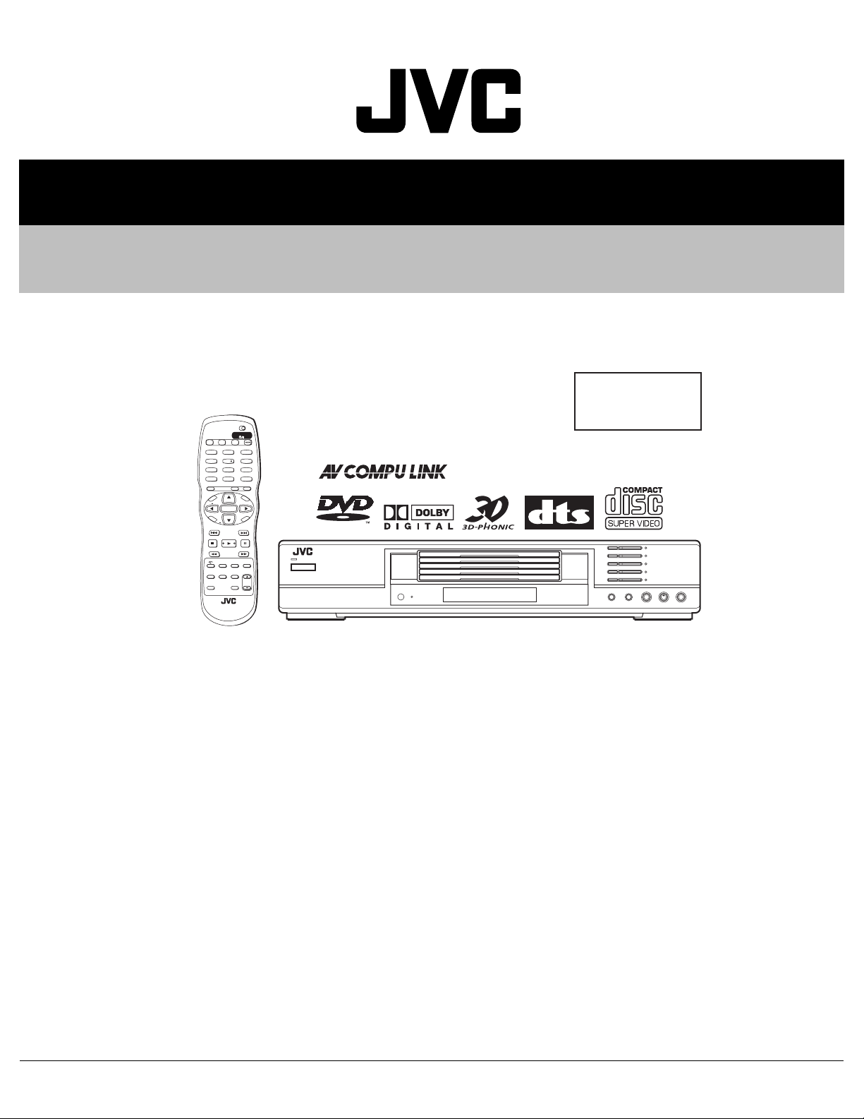
DVD VIDEO PLAYER
XA00820036
XV-M5GSL
Area Suffix
J -------------------- U.S. A.
TV DVD
STANDBY/ON
OPEN/
DISC
TV DVD
CLOSE
SELECT
TV1 TV2 TV3
2
1
3
TV4 TV5 TV6
5
4
6
TV7 TV8 TV9
8
7
9
TV-/-- TV0 MUTING
010 +10
TITLE/
TV/VIDEO
GROUP
CANCELRETURN
U
M
N
E
E
CH
N
M
U
+
P
O
T
VOL VOL+
ENTER
C
H
O
SLOW
ANGLE
REPEAT
N
CH
E
E
R
I
C
C
E
S
N
O
NEXTPREVIOUS
SELECTCLEAR
-
SLOW+
3D
VFPZOOM
PHONIC
PROGRESSIVE
SCAN
SUB TITLE
AUDIO
AMP
VOL
DIMMER
VIDEO
C ---------------- Canada
TABLE OF CONTENTS
1 PRECAUTION. . . . . . . . . . . . . . . . . . . . . . . . . . . . . . . . . . . . . . . . . . . . . . . . . . . . . . . . . . . . . . . . . . . . . . . . . 1-3
2 SPECIFIC SERVICE INSTRUCTIONS. . . . . . . . . . . . . . . . . . . . . . . . . . . . . . . . . . . . . . . . . . . . . . . . . . . . . . 1-7
3 DISASSEMBLY . . . . . . . . . . . . . . . . . . . . . . . . . . . . . . . . . . . . . . . . . . . . . . . . . . . . . . . . . . . . . . . . . . . . . . . 1-8
4 ADJUSTMENT . . . . . . . . . . . . . . . . . . . . . . . . . . . . . . . . . . . . . . . . . . . . . . . . . . . . . . . . . . . . . . . . . . . . . . . 1-20
5 TROUBLE SHOOTING. . . . . . . . . . . . . . . . . . . . . . . . . . . . . . . . . . . . . . . . . . . . . . . . . . . . . . . . . . . . . . . . . 1-26
COPYRIGHT © 2003 VICTOR COMPANY OF JAPAN, LIMITED
No.XA008
2003/7
Page 2
SPECIFICATION
General
Readable discs DVD VIDEO, DVD-R (Video format), DVDRW (Video format), +RW (Video format), SVCD, Video CD,
Audio CD (CD-DA), MP3/WMA format, JPEG, CD-R/RW (CD-DA, SVCD, Video CD, MP3/WMA format,
JPEG)
Video format NTSC, 480i (Interlaced scan)/480p (Progressive scan) selectable
Other
Power requirements AC 120 V, 60 Hz
Power consumption 12 W (POWER ON) 0.8 W (STANDBY mode)
Mass 4.2 kg (9.3 lbs)
Dimensions (W x H x D) 435mm x 83mm x 322mm (17-3/16 inch x 3-5/16 inc x 12-11/16 inch)
Video outputs
COMPONENT (pin jacks) Y Output: 1.0 Vp-p (75 ohm)
Pb/Pr Output: 0.7Vp-p (75 ohm)
VIDEO OUT (pin jack) 1.0 Vp-p (75 ohm)
S-VIDEO OUT (S jack) Y Output: 1.0 Vp-p (75 ohm)
C Output: 286 mVp-p (75 ohm)
Horizontal resolution 500 lines or more
Audio outputs
ANALOG OUT (pin jack) 2.0 Vrms (10 kohm)
DIGITAL OUT (COAXIAL) 0.5 Vp-p (75 ohm termination)
DIGITAL OUT (OPTICAL) -21 dBm to -15 dBm (peak)
Audio characteristics
Frequency response CD (sampling frequency 44.1 kHz):2 Hz to 20 kHz
DVD (sampling frequency 48 kHz):2 Hz to 22 kHz
(4 Hz to 20 kHz for DTS and Dolby Digital bitstream signals)
DVD (sampling frequency 96 kHz):2 Hz to 44 kHz
Dynamic range 16 bit: More than 98 dB
20 bit: More than 100 dB
24 bit: More than 100 dB
Wow and flutter Unmeasurable (less than ±0.002%)
Total harmonic distortion less than 0.006%
• Specifications and appearance are subject to change without prior notice.
• Manufactured under license from Dolby Laboratories. "Dolby" and the double-D symbol are trademarkes of Dolby Laboratories.
• "DTS" and "DTS Digital Out" are trademarks of Digital Theater Systems, Inc.
Digital output signal chart
Disc type Output
PCM ONLY DOLBY DIGITAL/PCM STREAM/PCM
DVD with 48/44.1 kHz,
16/20/24 bit linear PCM
DVD with 96 kHz,
16/22/24 bit linear PCM
DVD with DTS 48kHz, 16bit, stereo linear PCM DTS bitstream
DVD with Dolby Digital 48 kHz, 16 bit, stereo linear PCM Dolby Digital bitstream
DVD with MPEG
Multichannel
SVCD/Video CD/Audio CD 44.1 kHz, 16 bit, stereo linear PCM
Audio CD with DTS 48kHz, 16bit, stereo linear PCM DTS bitstream
CD-R/RW with MP3/WMA Linear PCM
48kHz, 16 bit, stereo linear PCM MPEG bitstream
48/44.1 kHz, 16 bit, stereo linear PCM
48kHz, 16 bit, stereo linear PCM (Down sampling)
1-2 (No.XA008)
Page 3
SECTION 1
PRECAUTION
1.1 Safety Precautions
(1) This design of th is product contains special hardw are and
many circuits and components specially for safety purposes. For continued protection, no changes should be made
to the original design unless authorized in writing by the
manufacturer. Replacement parts must be identical to
those used in the original circuits. Services should be performed by qualified personnel only.
(2) Alterations of the design or circuitry of the product should
not be made. Any design alterations of the product should
not be made. Any design alterations or additions will void
the manufacturers warranty and will further relieve the
manufacture of responsibility for personal injury or property
damage resulting therefrom.
(3) Many electrical and mechanical parts in the products have
special safety-related characteristics. These characteristics are often not evident from visual inspection nor can the
protection afforded by them necessarily be obtained by using replacement components rated for higher voltage, wattage, etc. Replacement parts which have these special
safety characteristics are identified in the Parts List of Service Manual. Electrical components having such features
are identified by shading on the schematics and by ( ) on
the Parts List in the Service Manual. The use of a substitute
replacement which does not have the same safety characteristics as the recommended replacement parts shown in
the Parts List of Service Manual may create shock, fire, or
other hazards.
(4) The leads in the products are routed and dressed with ties,
clamps, tubings, barriers and the like to be separated from
live parts, high temperature parts, moving parts and/or
sharp edges for the prevention of electric shock and fire
hazard. When service is required, the original lead routing
and dress should be observed, and it should be confirmed
that they have been returned to normal, after reassembling.
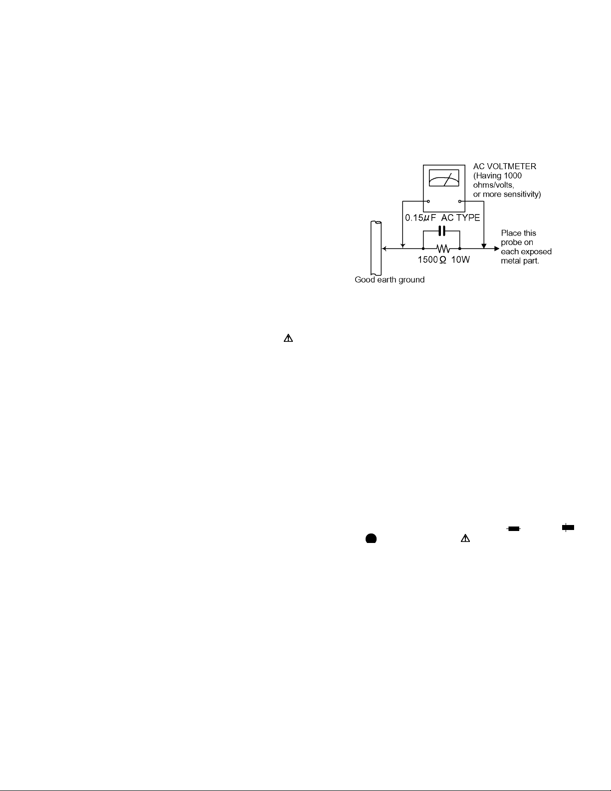
(5) Leakage shock hazard testing)
After reassembling the product, always perform an isolation check on the exposed metal parts of the product (antenna terminals, knobs, metal cabinet, screw heads,
headphone jack, control shafts, etc.) to be sure the product
is safe to operate without danger of electrical shock.Do not
use a line isolation transformer during this check.
• Plug the AC line cord directly into the AC outlet. Using a
"Leakage Current Tester", measure the leakage current
from each exposed metal parts of the cabinet, particularly any exposed metal part having a return path to the
chassis, to a known good earth ground. Any leakage current must not exceed 0.5mA AC (r.m.s.).
• Alternate check method
Plug the AC line cord directly into the AC outlet. Use an
AC voltmeter having, 1,000 ohms per volt or more sensitivity in the following manner. Connect a 1,500 ohm 10W
resistor paralleled by a 0.15 F AC-type capacitor between an exposed metal part and a known good earth
ground.
Measure the AC voltage across the resistor with the AC
voltmeter.
Move the resistor connection to each exposed metal
part, particularly any exposed metal part having a return
path to the chassis, and measure the AC voltage across
the resistor. Now, reverse the plug in the AC outlet and
repeat each measurement. Voltage measured any must
not exceed 0.75 V AC (r.m.s.). This corresponds to 0.5
mA AC (r.m.s.).
1.2 Warning
(1) This equipment has been designed and manufactured to
meet international safety standards.
(2) It is the legal resp onsibility of the repairer to ensure that
these safety standards are maintained.
(3) Repairs must be made in accordance with the relevant
safety standards.
(4) It is essential that safety critical compone nts are replaced
by approved parts.
(5) If mains voltage selector is provided, check setting for local
voltage.
1.3 Caution
Burrs formed during molding may be left over on some parts
of the chassis.
Therefore, pay attention to such burrs in the case of preforming repair of this system.
1.4 Critical parts for safety
In regard with component parts appearing on the silk-screen
printed side (parts side) of the PWB diagrams, the parts that are
printed over with black such as the resistor ( ), diode ( )
and ICP ( ) or identified by the " " mark nearby are critical for
safety. When replacing them, be sure to use the parts of the
same type and rating as specified by the manufacturer. (Except
the JC version)
(No.XA008)1-3
Page 4
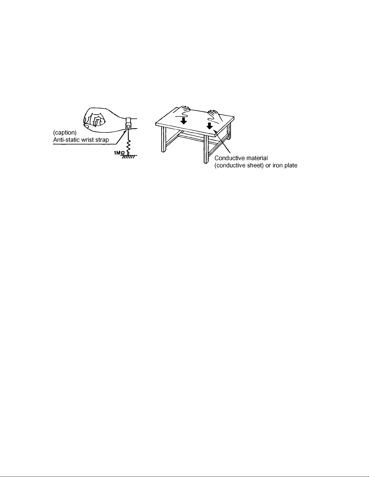
1.5 Preventing static electricity
Electrostatic discharge (ESD), which occurs when static electricity stored in the body, fabric, etc. is discharged, can destroy the laser
diode in the traverse unit (optical pickup). Take care to prevent this when performing repairs.
1.5.1 Grounding to prevent damage by static electricity
Static electricity in the work area can destroy the optical pickup (laser dio de) in devices such as DVD players.
Be careful to use proper grounding in the area where repairs are being performed.
(1) Ground the workbench
Ground the workbench by laying conductive material (such as a conductive sh eet) or an iron plate over it before placing the
traverse unit (optical pickup) on it.
(2) Ground yourself
Use an anti-static wrist strap to release any static electricity built up in your body.
(3) Handling the optical pickup
• In order to maintain quality during transport and before instal lation, both sides of the laser di ode on the replacement optica l
pickup are shorted. After replacement, return the shorted parts to their original condition.
(Refer to the text.)
• Do not use a tester to check the condition of the laser diode in the optical pickup. The tester's internal power source can easily
destroy the laser diode.
1.6 Handling the traverse unit (optical pickup)
(1) Do not subject the traverse unit (optical pickup) to strong shocks, as it is a sensitive, complex unit.
(2) Cut off the shorted part of the flexible cable using nippers, etc. after replacing the optical pickup. For specific details, refer to the
replacement procedure in the text. Remove the anti-static pin when replacing the traverse unit. Be careful not to take too long
a time when attaching it to the connector.
(3) Handle the flexible cable carefully as it may break when subjected to strong force.
(4) I t is not possible to adjust the semi-fixed resistor that adjusts the laser power. Do not turn it.
1-4 (No.XA008)
Page 5
1.7 Importance admistering point on the safety
B917
JT901 JT902
EP952
FC901
FC902
EP951
B915
P901
L901
C918
C902
C904 C905
B905
R910
D960
C951
R951
Q951
IC901
D901
B903
R913
D903
R906
R901
D902
C914
D904
B902
R912
PC901
C908
C913
R915
C907
R903
C916
CP951
B906
B907
D951
B908
C963
B909
D956
C964
C950
D952
B926
R954
L953
D957
T901
C953
B913
D954
B914
IC952
L954
C970
D955
D953
C958
C967
C952
C965
B920
C966
L955
L951
C973
L952
B918
Q953
C988
B924
B904
C955
B919
B927
B925
C959
B911
B912
C957
JT903 JT904
WC901
B923
EP910
B922
B921
B910
B916
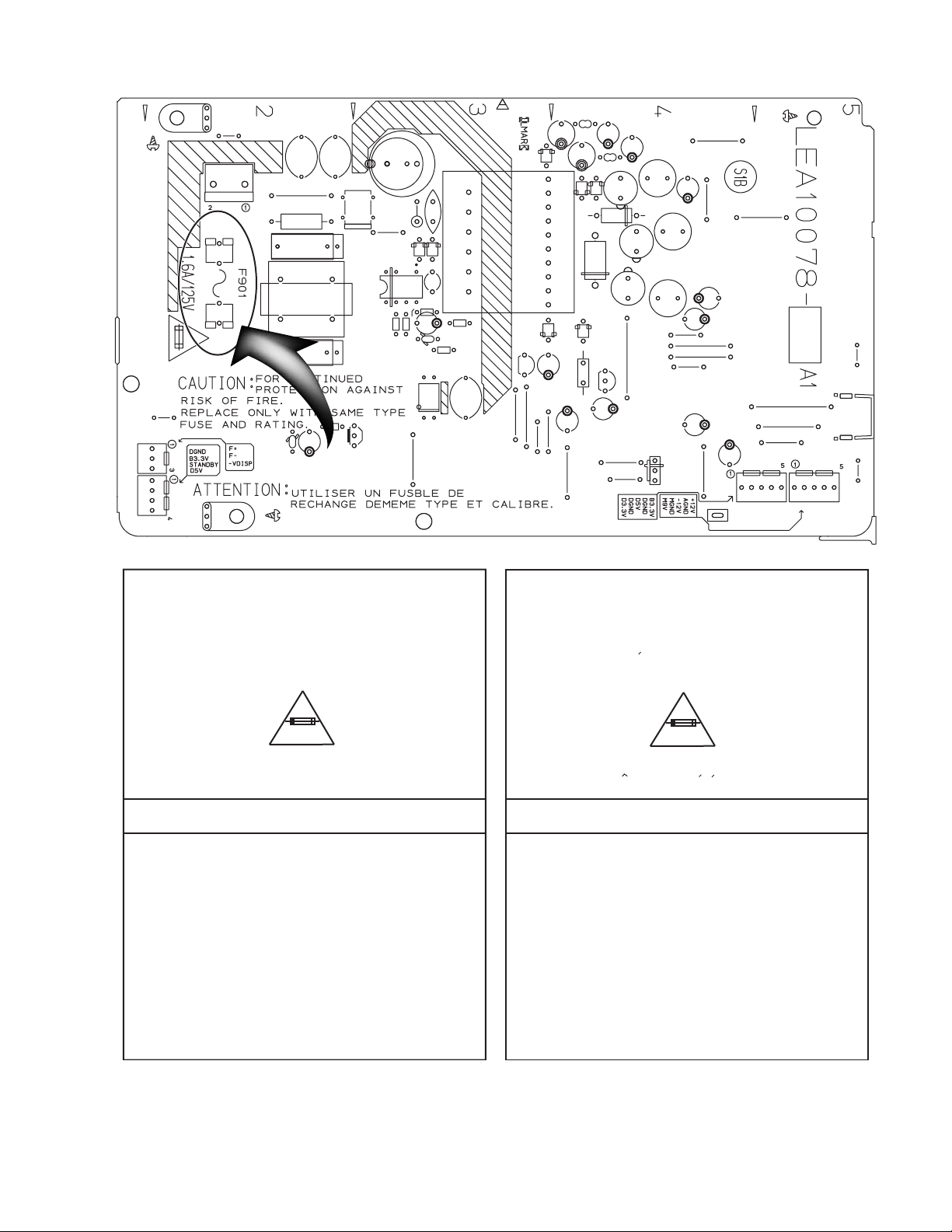
Full Fuse Replacement Marking
Graphic symbol mark
(This symbol means fast blow type fuse.)
should be read as follows ;
FUSE CAUTION
FOR CONTINUED PROTECTION AGAINST RISK
OF FIRE, REPLACE ONLY WITH SAME TYPE
AND RATING OF FUSES ;
F901 : 1.6 A / 125 V F901 : 1.6 A / 125 V
Marquage Pour Le Remplacement
Complet De Fusible
Le symbole graphique (Ce symbole signifie
fusible de type a fusion rapide.)
doit etre interprete comme suit ;
PRECAUTIONS SUR LES FUSIBLES
POUR UNE PROTECTION CONTINUE CONTRE
DES RISQUES D'INCENDIE, REMPLACER
SEULEMENT PAR UN FUSIBLE DU MEME TYPE ;
(No.XA008)1-5
Page 6
1.8 Precautions for Service
d
S
*Please refer to the disassembly method for detailes.
1.8.1 Handling of Traverse Unit and Laser Pickup
(1) Do not touch any peripheral element of the pickup or the actuator.
(2) The traverse unit and the pickup are precision devices an d therefore must not be subjected to strong shock.
(3) Do not use a tester to examine the laser diode. (The diode can easily be destroyed by the internal power supply of the tester.)
(4) To replace the traverse unit, pull out the metal short pin for protection from charging.
(5) When replacing the pickup, after mounting a new pickup, remove the solder on the short land which is provided at the center of
the flexible wire to open the circuit.
(6) Half-fixed resistors for laser power adjustment are adjusted in pairs at shipment to match the characteristics of the optical block.
Do not change the setting of these half-fixed resistors for laser power adjustment.
1.8.2 Destruction of Traverse Unit and Laser Pickup by Static Electricity
Laser diodes are easily destroyed by static electricity charged on clothingor the human body. Before repairing peripheral elements of
the traverse unit or pickup, be sure to take the following electrostatic protection:
(1) Wear an antistatic wrist wrap.
(2) With a conductive sheet or a steel plate on the workbench on which the traverse unit or the pick up is to be repaired, ground the
sheet or the plate.
(3) After removing the flexible wire from the connecto r (CN101), short-circuit the flexible wire by the metal clip.
(4) Short-circuit the laser diode by soldering the land which is provided at the center of the flexible wire for the pickup.
After completing the repair, remove the solder to open the circuit.
hort circuit
Short circuit
CN101
Servo control boar
1-6 (No.XA008)
Page 7

SECTION 2
SPECIFIC SERVICE INSTRUCTIONS
This service manual does not describe SPECIFIC SERVICE INSTRUCTIONS.
(No.XA008)1-7
Page 8
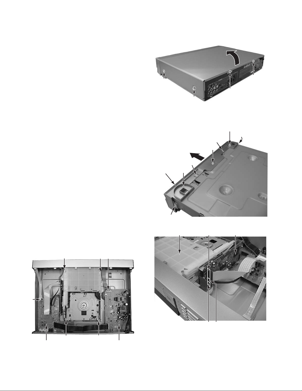
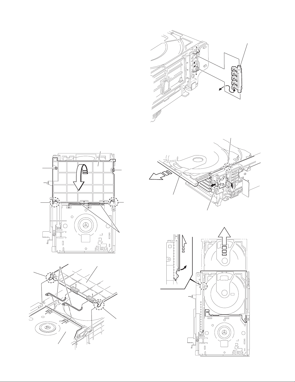
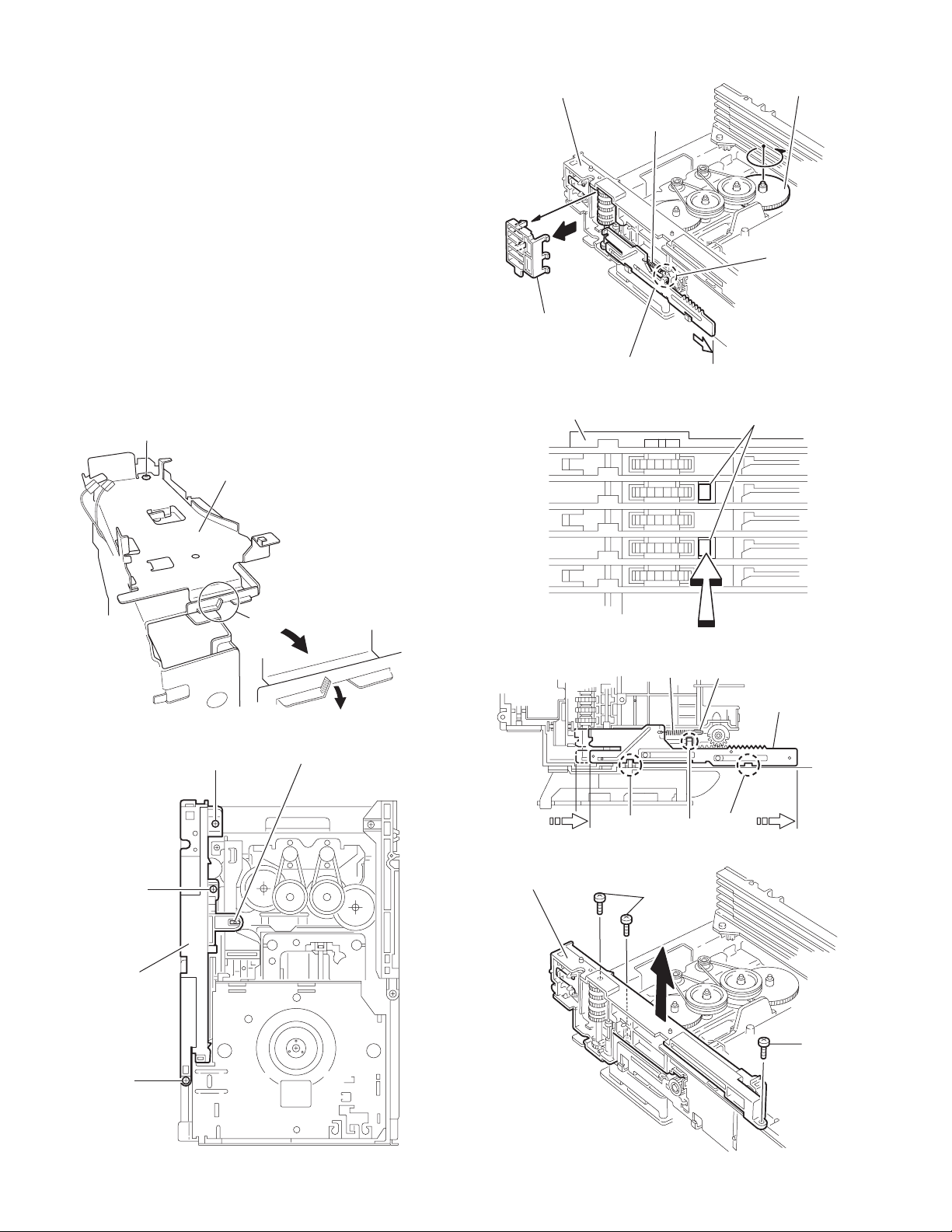
SECTION 3
TOP COVER
DISASSEMBLY
3.1 Main body section
3.1.1 Removing the top cover (See Figure 1)
(1) Remove the four screws A attaching the top cover on both
sides of the main body.
(2) Remove the two screws B attaching the top cover on the
back of the main body.
(3) Raise the both sides and lower part of the rea r of the top
cover, with opening them slightly in an outward direction.
And the top cover will be removed.
3.1.2 Removing the front panel assembly
(See Figure 2, Figure 3, Figure 4)
• Prior to performing the following procedure, remove the top
cover.
• There is no need to remove the mechanism assembly.
(1) Disconnect the flat wire from connector JT901, JT902 on
the power supply board.
(2) Disconnect the card wire from conne ctor CN501, CN702
on the servo control board and signal output terminal board
respectively.
(3) Remove the three screws C attaching th e front panel as-
sembly on the bottom of the main body.
(4) Hook a and b are removed respectively, and the front panel
assembly is removed.
3.1.3 Removing the changer mechanism assembly
(See Figure 2, Figure 4)
• Prior to performing the following procedure, remove the top
cover.
• There is no need to remove the front panel assembly.
(1) Disconnect the card wire from connector CN501, CN502,
CN503 on the servo control board.
(2) Remove the four screws D attaching the changer mecha-
nism assembly.
TOP COVER
TOP COVER
A x 2
A x 2
Fig.1
Front panel
assembly
Hook a
Mechanism assembly Servo control boardCN502
Hook b
C
Fig.3
B
B
C
Hook a
Hook b
C
CN702
Signal output terminal board
1-8 (No.XA008)
D
D
Fig.2
JT901,JT902
D
D
Power supply board
CN501 CN503
Fig.4
Page 9
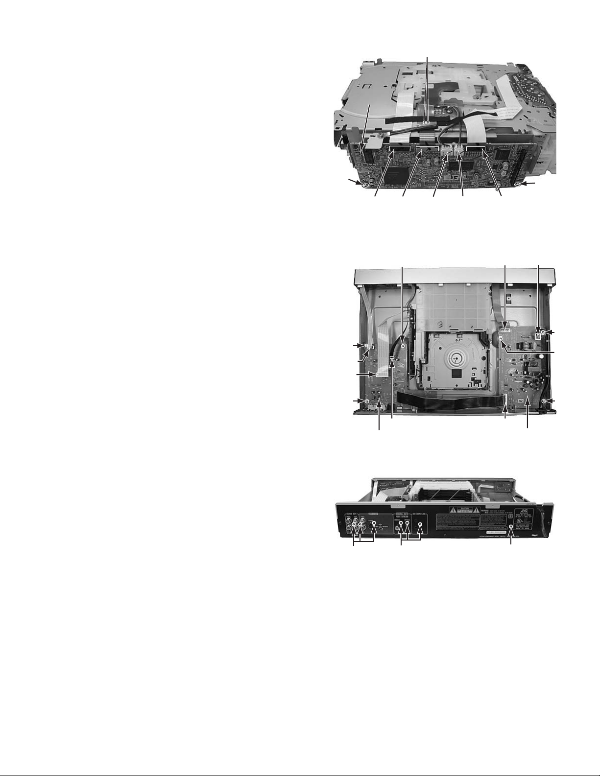
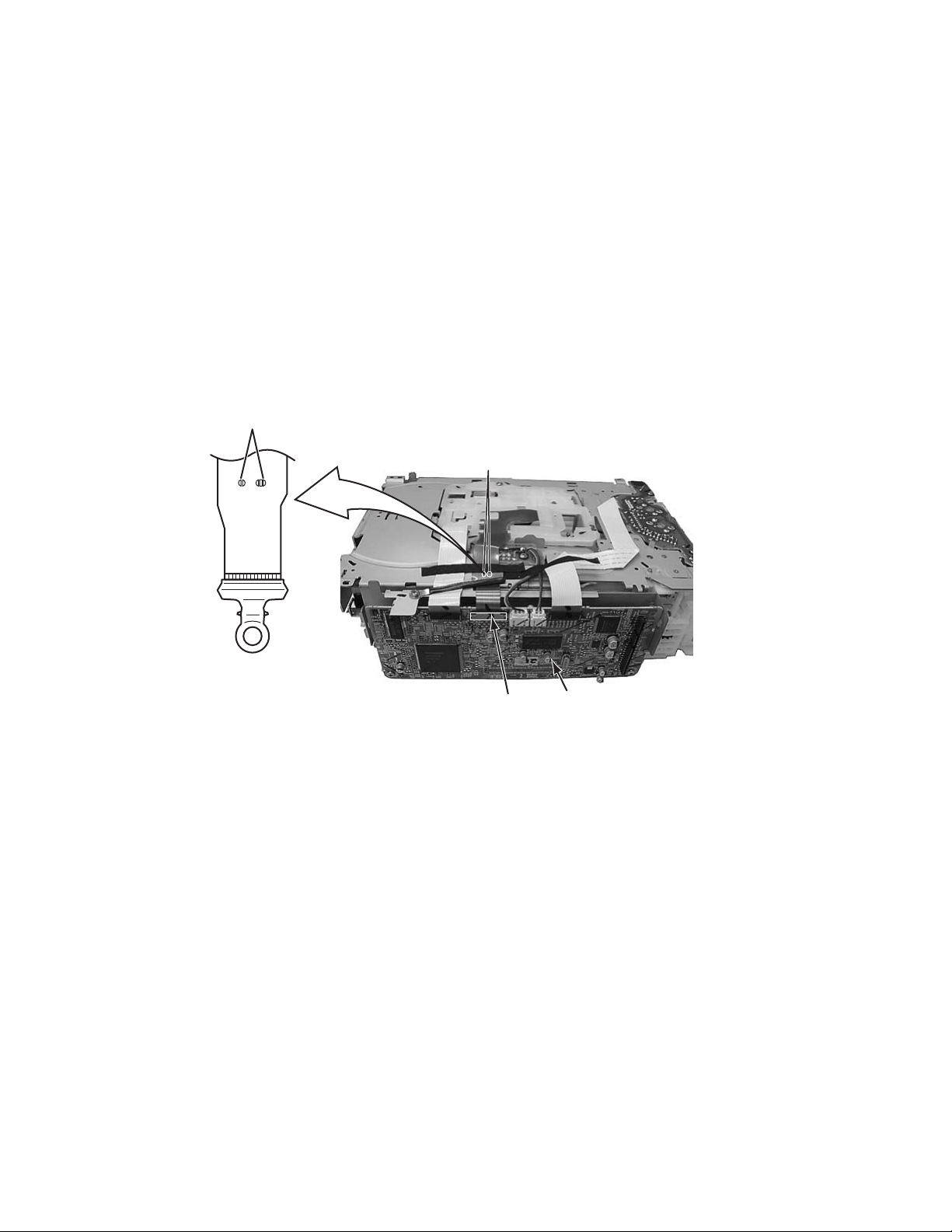
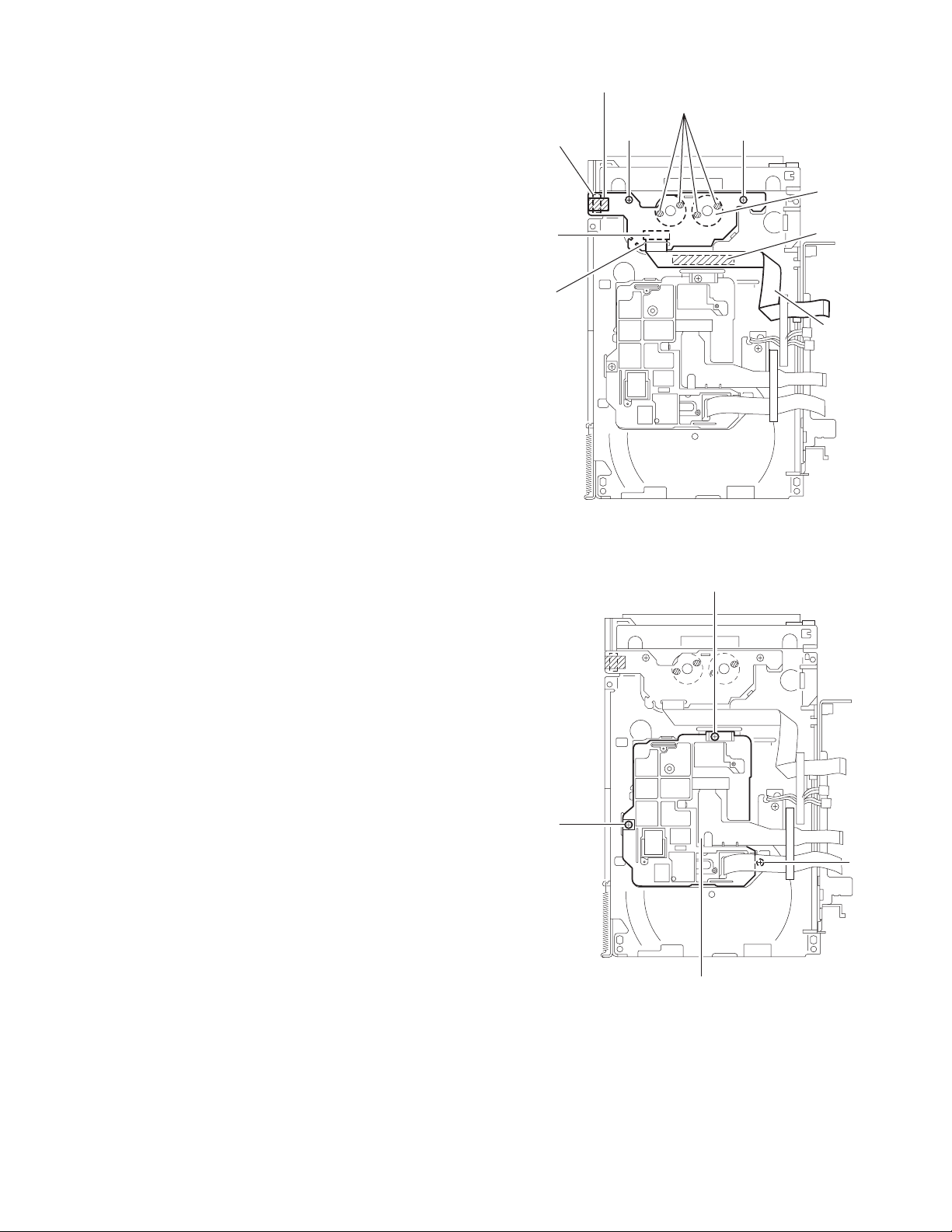
3.1.4 Removing the servo control board (See Figure 5)
Servo
control board
• Prior to performing the following procedure, remove the chang-
er mechanism assembly.
(1) Disconnect the card wire from connector CN101, CN103,
CN104, CN105, CN201 on the servo control board.
ATTENTION :
At this time, please extract the wire after short-circuited
of two places on the wire in part c with solder. Please remove the solder two places of part c after connecting the
wire CN101 when reassembling.
(2) Remove the two screws E attaching the servo control
board.
Servo
control board
E
Par t c
E
3.1.5 Removing the power supply board (See Figure 6, Figure 7)
• Prior to performing the following procedure, re move the top
cover.
(1) Disconnect the flat wire from connector JT901, JT902,
JT903, JT904 on the power supply board.
(2) Disconnect the socket wire from connector P901 on the
power supply board.
(3) Remove the three screws F attaching the power supply
board.
(4) Remove the one screw G attaching the power supply board
on the back of the main body.
3.1.6 Removing the signal output terminal board
(See Figure 6, Figure 7)
• Prior to performing the following procedure, re move the top
cover.
(1) Disconnect the card wire from connector CN601, CN701,
CN702 on the signal output terminal board.
(2) Disconnect the flat wire from connector JT903, JT904 on
the power supply board.
(3) Remove the three screws H attaching the signal output ter-
minal board.
(4) Remove the six screws I attaching the signal output termi-
nal board on the back of the main body.
CN201
CN101 CN105 CN104 CN103
H
H
CN702
CN601
H
CN701
Signal output terminal board
Fig.5
Fig.6
JT901,JT902
JT903,JT904
Power supply board
P901
F
F
F
I
I
G
Fig.7
(No.XA008)1-9
Page 10
3.2 Changer mechanism Section
r
3.2.1 Removing the tray assembly
(See Figs.1 to 5)
(1) Remove the two screws A from the top cover and release
the two joints a on both sides of the body.
(2) Remove the top cover with the two rods attached to the top
cover and lifter assembly respectively.
(3) Remove the open det lever on the left side of the body.
(4) Push part b of the slide (R) assembly on the right side of
the body to unlock the tray assembly. Draw out the trays to-
ward the front.
Attention:
The tray can be locked if all tray assemblies are attached.
(5) From top of the body, move the stopper tab c in the direc-
tion of the arrow and release. Pull out the tray assemblies
from the body.
Caution:
Remove the tray assembly from top tray 5 in order.
Attention:
When reattaching the sub tray of the tray assembly, or when
removing the DISC remaining inside, refer to another section.
Top cover
Open det leve
Fig.3
c
A
a
Lifter assembly
a
Rod
Fig.1
Top cover
A
a
Tray assembly
(Tray 5)
b
Fig.4
Rod
1-10 (No.XA008)
a
Lifter assembly
Fig.2
Fig.5
Page 11
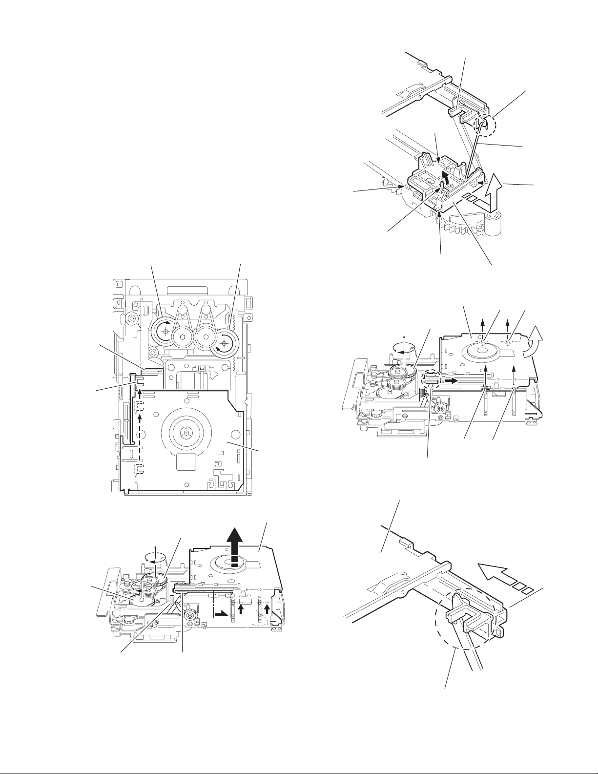
3.2.2 Removing the motor board
(See Fig.6)
(1) Unsolder the four soldered parts on the motor of the motor
board.
Caution:
If removing the motor board with the motor, you should
remove the screws attaching the motor from top of the
body(Refer to another section).
(2) Remove the two screws B attaching the motor board.
(3) Remove the spacer fixing the motor board and tray switch
board, and disconnect connector CN2 on the motor board.
(4) Disconnect the card wire from connector CN1 on the motor
board.
Caution:
When reconnecting the card wire, let the card wire through the
slot d of the motor board and attach it to the bottom of the body
using a double tape.
3.2.3 Removing the traverse mechanism assembly
(See Fig.7)
• Prior to performing the following procedure, remove the servo
control board.
(1) Turn over the body and remove the three screws C attach-
ing the tramecha.
CN2
CN1
d
Spacer
Soldering point
B
B
Motor
Double
face tape
Card wire
Fig.6
C
C
C
Traverse mechanism assembly
Fig.7
(No.XA008)1-11
Page 12
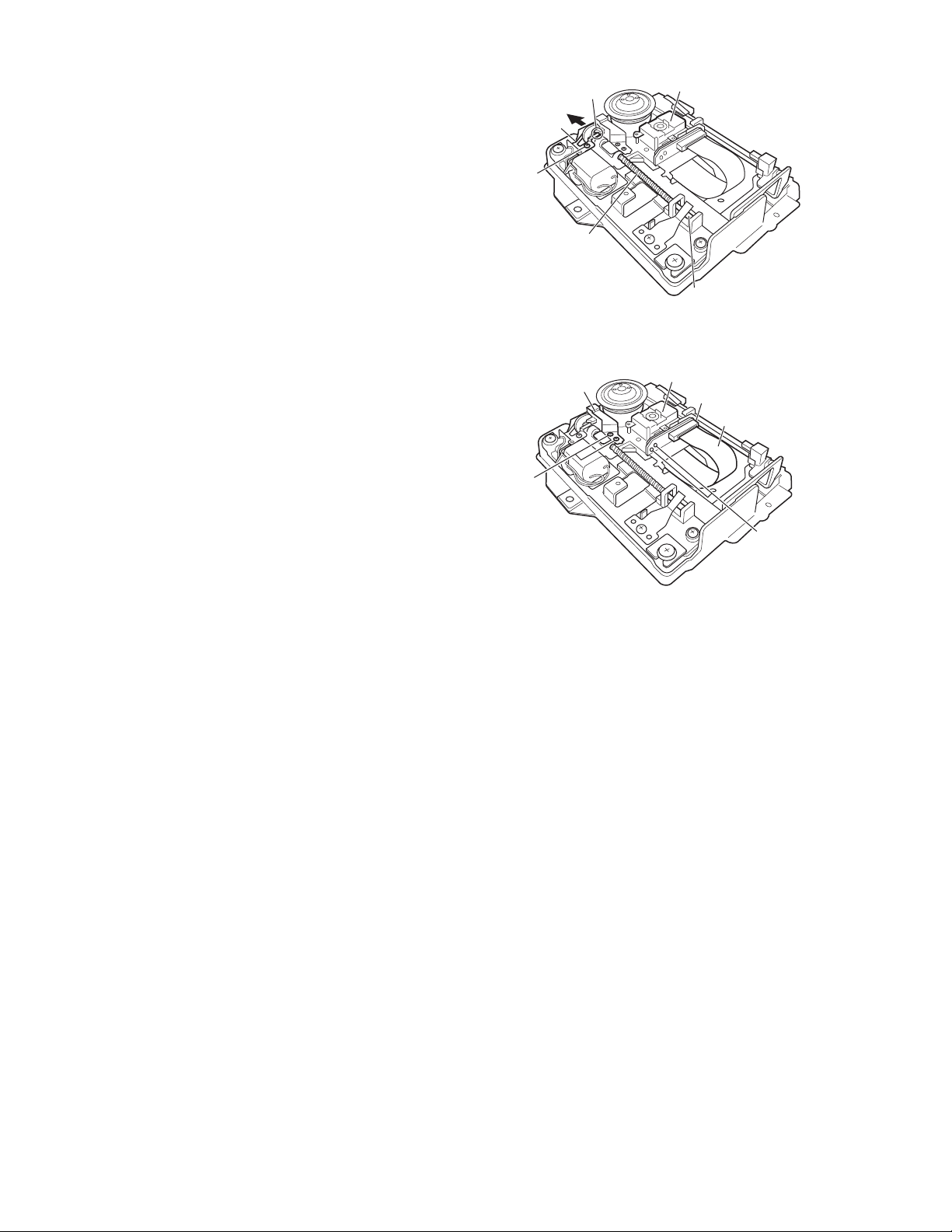
3.2.4 Removing the pickup
(See Fig.8-1, 8-2)
• Prior to performing the following procedure, remove the servo
control board and traverse mechanism assembly.
(1) Remove one screw D attaching the bracket. Then the
bracket is also removed.
(2) Slide e part of the worm shaft slightly in a direction of the
arrow, and pull out the worm shaft while lifting the worm
shaft in a direction of the arrow.
• The guide collar is also removed.
• Be sure to solder the short round point f on the pickup before removing the flexible wire from the pickup. In assembling procedure, connect the flexible wire to the
connector, and then be sure to unsolder the short round
point.
• Insert the guide collar in the worm shaft before attaching
the pickup.
(3) Remove the two screws E attaching the rack pl ate, a nd re-
move the rack plate.
(4) Pull out the worm shaft from the pickup.
Braket
D
Worm shaft
Rack plate
E
Part e
Pick-up
Guide collar
Fig.8-1
Pick-up
Connector
Flexible wire
Fig.8-2
Part f
1-12 (No.XA008)
Page 13
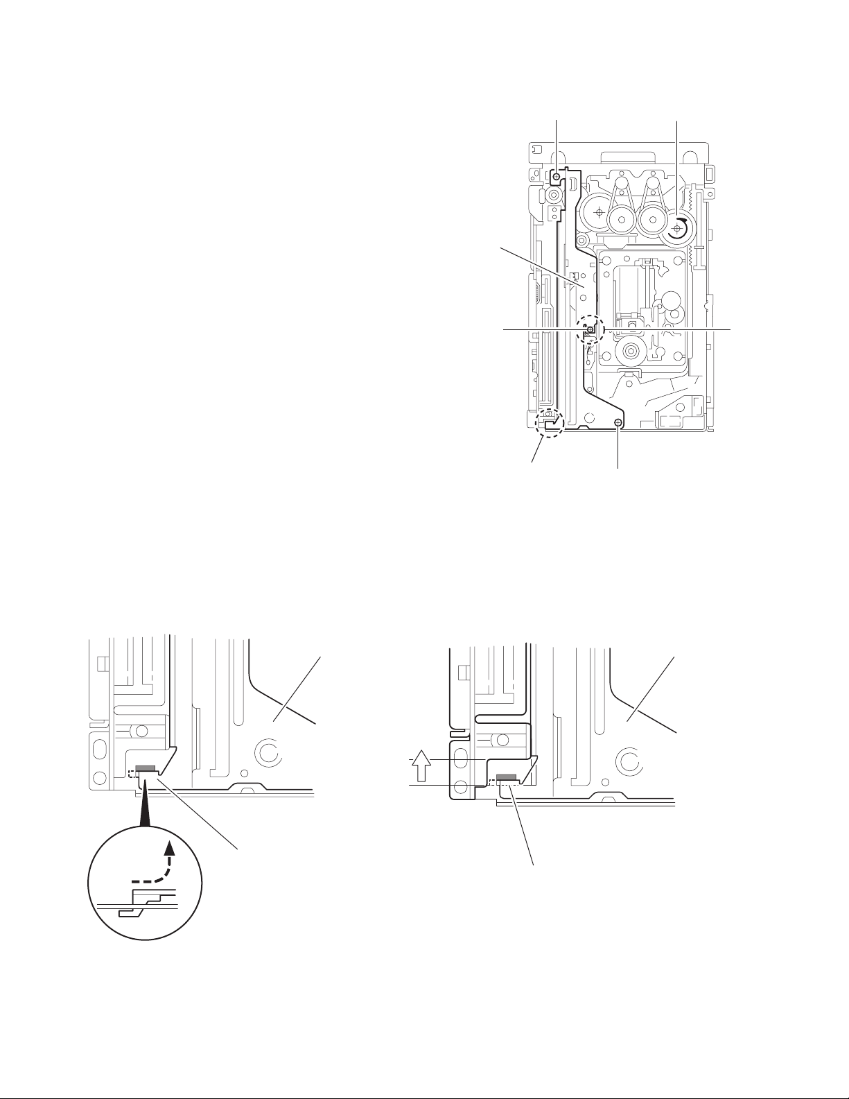
3.2.5 Removing the side (L)/ tray switch board
(See Figs.9 to 11)
• Prior to performing the following procedure, remove the tray
assembly.
(1) Remove the two screws F attaching the si de (L) on top of
the body.
(2) From the side of the body, remove the spacer fixing the tray
switch board and motor board. Disconnect connector CN3
on the tray switch board and detach the side (L) upward.
(3) Remove the screw G attaching the tray switch board.
(4) Push the joint tab g of the side (L) in the direction of the ar-
row and remove the tray switch board outward, then re-
lease joint h.
F
F
F
CN3
Spacer
Side (L)
Fig.9
Side (L)
F
Fig.10
g
Side (L)
h
G
Tray switch board
Fig.11
(No.XA008)1-13
Page 14
3.2.6 Removing the side (R) assembly
(See Figs.12 to 17)
• Prior to performing the following procedure, remove the tray
assembly.
(1) Bend i part of the bracket in a direction of the arrow by us-
ing pliers.
(2) Remove the one screw H attaching the bracket.
(3) Push and release the two tabs j of the gear co ver through
the two notches inside the side (R) assembly. Remove the
gear cover outward.
(4) Remove the spring attached to part k of the hook on the
right side of the body.
(5) From top of the body, turn the gear 1 clockwise to move the
elevator cam rearward.Move the two slots l and joint m of
the elevator cam as shown in Fig.16 and remove the ele-
vator cam outward.
(6) Remove the three screws I and detach the side (R) upward.
Caution:
When reattaching the side (R) assembly, make sure to fit the
shaft(part n) into the slot of the select lever.
H
Braket
Side (R) assembly
Gear cover
Elevator com
Side (R) assembly
gear 1
Spring
k
Fig.14
j
Side (R)
assembly
Part i
Fig.15
Spring
Fig.12
I
n
l
Fig.16
I
Side (R) assembly
I
m
k
Elevator cam
l
I
I
1-14 (No.XA008)
Fig.13
Fig.17
Page 15
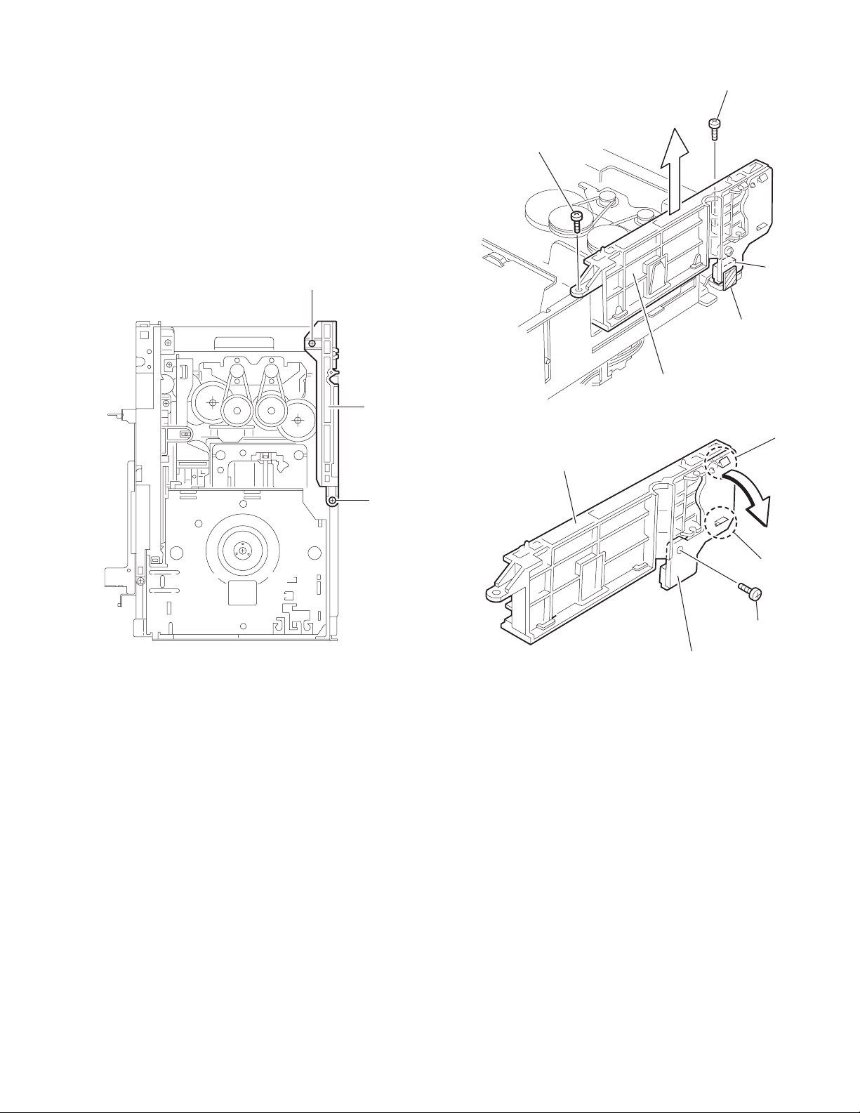
3.2.7 Removing the lifter assembly
(See Figs.18 to 22)
• Prior to performing the following procedure, remove the tray
assembly and side (L)/ side (R) assembly.
(1) From top of the body, turn the gear 1 clockwise to move the
lifter assembly upward as shown in Fig.19.
(2) From top of the body, turn the gear 2 clockwise to move the
hook toward the front until it stops.
(3) Move the hook stopper in the d irection of the arrow while
pushing the tab o of the hook stopper to unlock it. Release
four joints p to detach from the rack holder.
Release the rod from part q.
(4) Turn the gear 1 clockwise again to move the lifter assembly
upward.
(5) Remove the lifter assembly from the body upward at posi-
tion r where the four pins on the right and left sides of the
lifter assembly fit to the notches of the s.
Move the lifter assembly toward the front and release from
the hook.
Gear 2
Gear 1
Hook
q
p
Rod
p
p
o
p
Hook stopper
Fig.20
Lifter assembly
Gear 1
r r
Hook stopper
Hook
Gear 2
Fig.18
Gear 1
Lifter
assembly
Lifter assembly
s
Lifter assembly
Fig.21
r
r
Hook stopper
Hook
Fig.19
s
Fig.22
(No.XA008)1-15
Page 16
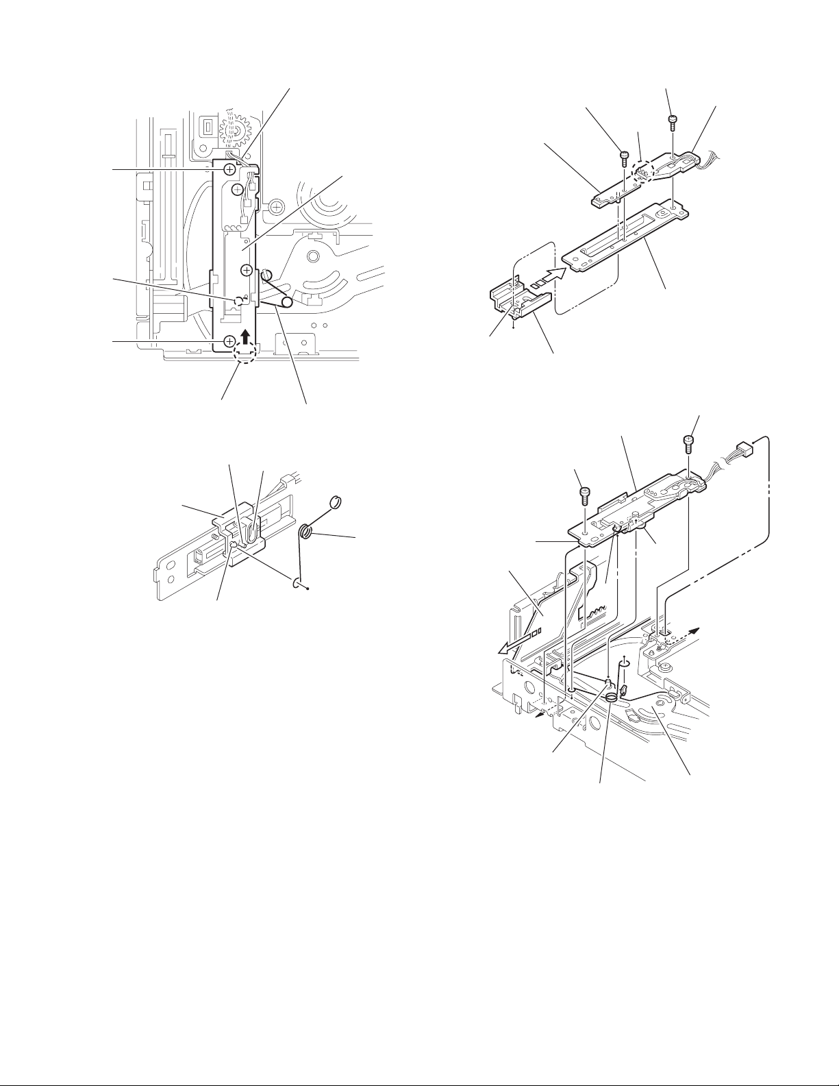
3.2.8 Removing the rack holder assembly/ sensor assembly
(See Figs.23 to 28)
• Prior to performing the following procedure, remove the tray
assembly, side (L)/ side (R) assembly, lifter assembly.
Attention:
If the slide gear of the body places at joint t of the rack holder
assembly, turn the gear 1 countercl ockwise to move the slide
gear toward the front. Remove the rack holder assembly.
(1) Remove the three screws J attaching the rack holder as-
sembly. Release joint t from the notch.
Caution:
When reattaching the rack holder assembly, do not nip
the wire u extending from the sensor assembly.
(2) Remove the two screws K attaching the sensor assembly.
(3) Move the sensor assembly in the direction of the a rrow to
release from the slot at joint v.
(4) Remove the spring attached to the bottom of the sensor as-
sembly from the boss w on the sensor slider.
(5) Remove the screw L and M attaching the sensor board and
SV resister respectively.If necessary, unsolder the sensor
board.
Caution:
When reattaching the SV resister, attach the sensor slider to
the sensor bracket and fit the lever on the bottom of the SV resister into slot x of the sensor slider.
Caution:
When reattaching the rack holder assembly, turn the gear 1
clockwise to move the slide gear and slide lever inside the
body rearward.
• Let the wire extending from the sensor assembly through notch
u to the bottom of the body.
•Fit pin y of the slide lever into hole z of the sensor slider on the
bottom of the sensor assembly while attaching the spring to the
boss w of the sensor slider.
• Engage joint v of the sensor assembly to the notch of the body.
Rack holder
assembly
Rack holder
assembly
J
J
Gear 1
u
t
J
Fig.23
Rack holder
assembly
1-16 (No.XA008)
t
t
Fig.24
Page 17
u
M
Soldering
SV resister
L
Sensor board
point
K
w
K
Sensor slider
v
x
Fig.25
Sensor assembly
Sensor braket
x
Sensor slider
Fig.27
Spring
Sensor assembly
z
Spring
Slide gear
v
K
K
z
w
Fig.26
w
y
Spring
Fig.28
Slide lever
(No.XA008)1-17
Page 18
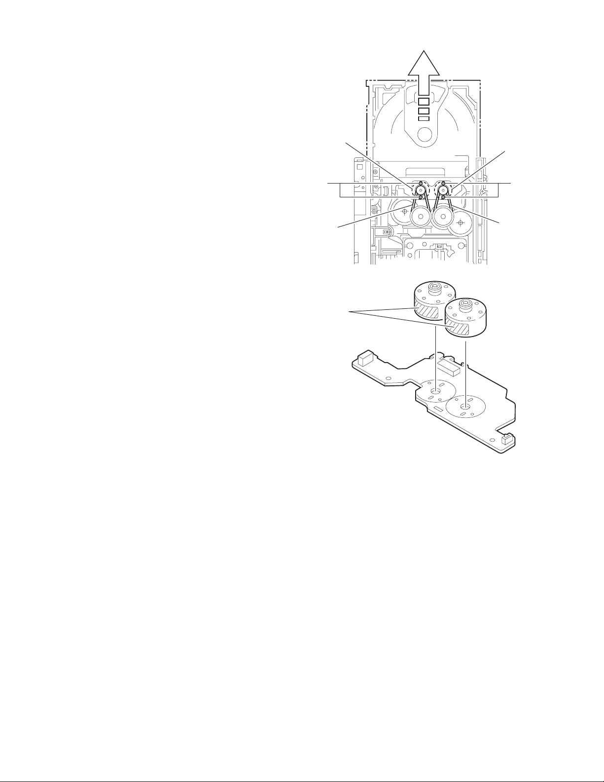
3.2.9 Removing the motor
r
(See Fig.29, 30)
• Prior to performing the following procedure, remove the servo
control board and top cover.
Attention:
You need not to remove the tray assembly, and in such case,
move it.
(1) Remove the two belts on top of the body.
(2) Remove the four screws N attaching the motor.
(3) Remove the motor board from the bottom of the body.
(Refer to the section “Removing the motor board”.)
Attention:
When removing the motor board with the motor, you need not
to unsolder four soldered parts.
Caution:
When reattaching the motor, turn the side where the label
should be put to the front side.
Motor
Moto
NN
Belt
Fig.29
Label
Belt
Fig.30
1-18 (No.XA008)
Page 19
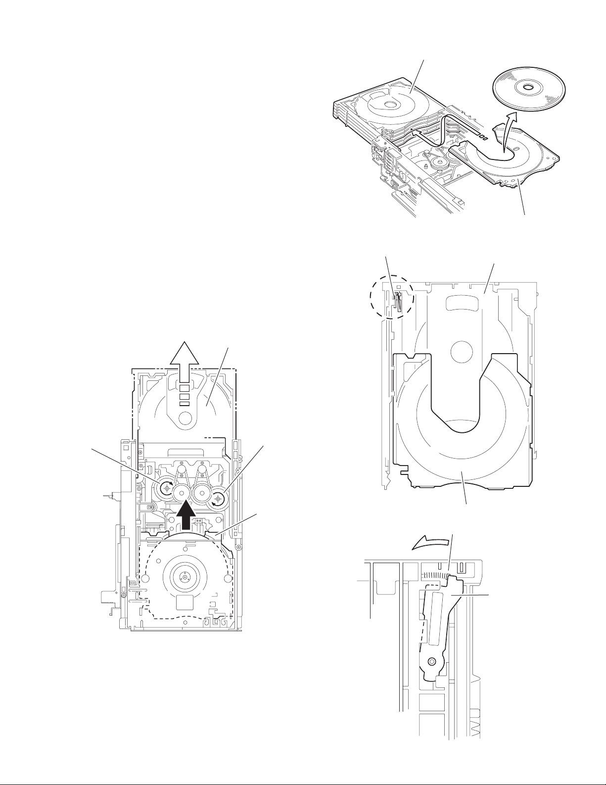
3.2.10 Taking out the DISC in play mode
r
(See Figs.31 to 34)
• Prior to performing the following procedure, re move the top
cover.
• You can perform the procedure above even if you don't remove the changer mechanism assembly from the chassis of
the unit.
(1) Remove the three screws attaching the front panel assem-
bly, and move the front panel assembly in the front direc-
tion slightly.
(2) Remove the top cover upward.
(3) Unlock the tray assembly and draw out the tray assembly
toward the front.
(4) From top of the body, turn the gear 1 clockwise to move the
lifter assembly upward.
(5) From top of the body, turn the gear 2 clockwise to move the
sub tray remaining inside the lifter assembly toward the
front, then pull out.
(6) Take out the DISC on the sub tray.
(7) After clearing away the DISC, insert the sub tray into the
main tray.
Caution:
When reattaching the sub tray, move the tray stopper on
the bottom of the main tray in the direction of the arrow
to lock the sub tray certainly.
(8) Push the tray assembly toward the body and reattach.
Tray assembly
Tray assembly
Tray stopper
Sub tray
Fig.32
Main tray
Gear 2
Fig.31
Gear 1
Sub tray
Sub tray
Fig.33
Tray stoppe
Fig.34
(No.XA008)1-19
Page 20

SECTION 4
ADJUSTMENT
4.1 Test mode setting method
(1) Unplug the power plug.
(2) Insert power plug into outlet while pressing both "PLAY" key and "STOP" key of the main body.
(3) The FL display shows "∗0", and the main body turns to test mode. "∗" means the de stination, and "0" means parameter adjust-
ment status.
(4) To release test mode, press "POWER" key of the main body.
NOTE:
Each pressing of "CHOICE" key of the remote controller in test mode changes the mode as follows.
0 ---------------------------
_ _ ---------------
Becames test mode
Version of firmware
FL Display becames all lighting
CHECK --------------------------
EXPERT -------------------------
4.2 Method of displaying version of firmware
(1) Set the main body at test mode.
(2) Press "CHOICE" key of the remote controller once. Then, versio n number and alphabe tical letter of the system controller and
the back end are displayed in the FL display as follows:
Check mode
Not used
FL Display (Example)
34_02_57
Back end
Front end
System controller
4.3 Initialization method
Please initialize according to the following procedures in the following case:
• Just after you upgrade the firmware.
• After you confirm the symptoms that a customer points out. First Initialize, and then confirm whether the symptoms are improved or
not.
• After servicing, before returning the main body to a customer. (Initialized main body should be returned to a customer.)
(1) Set the main body at test mode.
(2) Press "PAUSE" key of the main body.
(3) When initialization is completed, the FL display changes from "∗0" to "∗00".(The le ft "0" of "00" is not always "0". It shows pa-
rameter adjustment status.)
OPEN/
DISC
CLOSE
SELECT
TV1 TV2 TV3
1
TV4 TV5 TV6
4
TV7 TV8 TV9
7
TV-/-- TV0 MUTING
U
N
E
CH
M
+
P
O
T
VOL VOL+
ENTER
C
CH
H
O
I
C
E
SELECTCLEAR
-
SLOW
3D
PHONIC
SUB TITLE
ANGLE
REPEAT
1-20 (No.XA008)
TV DVD
STANDBY/ON
TV DVD
2
5
8
010 +10
TITLE/
GROUP
AUDIO
DIMMER
TV/VIDEO
CANCELRETURN
N
O
NEXTPREVIOUS
SLOW+
PROGRESSIVE
3
6
9
M
E
N
U
N
E
E
R
C
S
VFPZOOM
SCAN
AMP
VOL
CHOICE key
(switch of mode)
POWER key
FL Display
STOP key
(for test mode)
PAUSE key
(for initialize)
PLAY key
(for test mode)
Page 21

4.4 All-initialization method
Please perform all-initialization according to the following procedures in the following case:
• Just after you exchange the pick-up.
• Just after you exchange the spindle motor.
• Just after you exchange the traverse mechanism base.
NOTE:
Please perform all-initialization when you exchange the parts above and also when you remove the parts above.
• Just after the flap adjustment of the pick-up guide shaft
(1) Set the main body at test mode.
(2) Press and hold "BACKWARD SKIP" key of the main body fo r more than 2 seconds.
(3) When all-initialization is completed, the FL display changes from "∗0" to "∗33".
NOTE:
After all-initialization, be sure to perform optimization adjustment of Front End parameter.
4.5 Optimization adjustment of Front End parameter
Adjustment to optimize Front End parameter must be performed in each mechanism assemb ly of this model for high-speed starting.Please perform optimization according to the following p rocedures just after all-initialization i s completed and when FL display
shows anything except "∗0" (For example when FL display shows "∗1", "∗2", and "∗3") at test mode.
(1) Press "POWER" key of the main body to turn the main body on (not to set the main body at test mode).
(2) Insert the test disc VT-501 or commercial dual-layer DVD software.
(3) Remove the disc when the FL display changes from "READING" to disc information.
(4) Perform the same procedures as in (2) and (3) above by using the test disc CTS-1000 or commercial CD-DA softw are.
(5) Set the main body at test mode, and check that the FL display shows "∗0".
NOTE:
Status of this adjustment can be judged by the number displayed at test mode as follows:
DVD adjustment CD adjustment FL display at test mode
Adjusted Adjusted ∗0
Not adjusted Adjusted ∗1
Adjusted Not adjusted ∗2
Not adjusted Not adjusted ∗3
NOTE:
As for a disc used for adjustment,
• Disc should be mounted. ("Mounting" means to display "READING" after the disc is inserted and then display the disc information.) Disc need not be played.
• If you do not have test disc either VT-501 (DVD) or CTS-1000 (CD-DA), use a commercial disc (for DVD, dual-layer software) after seeing and checking that the di sc is neit her curved nor foreseen that it may shake at the time of playback.If you
use a disc with bad features, starting time may be slow or disc may not be read.
TV DVD
STANDBY/ON
OPEN/
DISC
TV DVD
CLOSE
SELECT
TV1 TV2 TV3
2
1
3
TV4 TV5 TV6
5
4
6
TV7 TV8 TV9
8
7
9
TV-/-- TV0 MUTING
010 +10
TITLE/
TV/VIDEO
GROUP
CANCELRETURN
U
M
N
E
E
CH
N
M
U
+
P
O
T
VOL VOL+
ENTER
C
N
CH
H
E
O
E
R
I
C
C
E
S
N
O
NEXTPREVIOUS
SELECTCLEAR
-
SLOW+
SLOW
3D
VFPZOOM
PHONIC
PROGRESSIVE
SCAN
SUB TITLE
ANGLE
AUDIO
AMP
VOL
REPEAT
DIMMER
POWER key
FL Display
STOP key
(for test mode)
BACKWARD SKIP key
(for All initialize : It pushes 2 seconds or more.)
PLAY key
(for test mode)
(No.XA008)1-21
Page 22

4.6 Display of current value of laser
(1) Set the main body at test mode.
(2) Press "CHOICE" key of the remote controller three times. T hen, FL display is displayed "CHECK".
(3) The laser current value can be switched between th e value of CD and that of DVD by pressing the following key of the re mote
controller.
FL Display (Example)
1419 0000
The number shown in the FL display shows mA of current value of laser.
The first two numbers ("14" in "1419") shows current value of laser at the time of adjustment after the latest all-initialization, 14mA
in this example.
The last two numbers ("19" in "1419") shows the present current value of laser, 19mA in this example.
The first two numbers ("14" in "1419") usually shows current value of laser at the time of shipment, so you can see how the product has been deteriorated by comparing the first two numbers ("14" in "1419") and the last two numbers ("19" in "1419").
CD and DVD:
The laser current value of 80 mA or less is normal.The laser current value of over 81 mA is n ot normal. Laser diode of the
pickup has been deteriorated.
To return to test mode, press "STOP" key of the main body.
4.7 Flap adjustment of the pick-up guide shaft
Please perform flap adjustment of the pick-up guide shaft in the following case:
• Just after you exchange the pick-up.
• Just after you exchange the spindle motor.
• Just after you exchange the traverse mechanism base.
NOTE:
Please perform flap adjustment of the pick-up guide shaft when you exchange the parts above and also when you remove the
parts above.
• When the reading accuracy of the signal is bad (There is a block noise in the screen, Screen stops in the outer circumference of a
disc, etc.)
4 key (laser of CD)
5 key (laser of DVD)
TV DVD
STANDBY/ON
OPEN/
DISC
TV DVD
CLOSE
SELECT
TV1 TV2 TV3
2
1
3
TV4 TV5 TV6
5
4
6
TV7 TV8 TV9
7
TV-/-- TV0 MUTING
U
N
E
CH
M
+
P
O
T
VOL VOL+
ENTER
C
CH
H
O
I
C
E
SELECTCLEAR
-
SLOW
3D
PHONIC
SUB TITLE
ANGLE
REPEAT
6 key
8
9
(display of jitter value)
010 +10
TITLE/
TV/VIDEO
GROUP
CANCELRETURN
M
E
N
U
CHOICE key
N
E
E
R
C
(switch of mode)
S
N
O
NEXTPREVIOUS
SLOW+
VFPZOOM
PROGRESSIVE
SCAN
AUDIO
AMP
VOL
DIMMER
POWER key
Remote controller "4" key --- Laser of CD
Remote controller "5" key --- Laser of DVD
(for test mode and jitter value)
FL Display
STOP key
(for test mode)
PLAY key
1-22 (No.XA008)
Page 23

4.7.1 Tool for adjustment
*Stud: One set (four studs), Part number: JIGXVS40
4.7.2 Preparation for adjustment
(1) See the disassembly procedure, and remove the changer mechanism assembly from the main body.
(2) Remove the servo control board attached to the changer mechanism assembly.
(If you disconnect the wires connected to the servo control board, connect them again.)
(3) Attach the four studs to the changer mechanism assembly.
(4) Put the changer mechanism a ssembly in the center of the main body, and connect the card wire from the connector CN501,
CN502, CN503 on the servo control board.
Stud
Changer mechanism assembly
Servo control board
Stud
Changer mechanism assembly
4.7.3 Adjustment
(1) Set the unit to test mode.
(2) Press the "CHOICE" key of the remote controller three times, and the FL display is displayed "CHECK".
(3) A PLAY key is pushed after insert a test disc (VT-501), and press the numeric key "1" of the remote controller for automatic
adjustment.
(4) After a few seconds, press the numeric key "6" of the remote controller. Then, the FL display displays a jitter value.
(5) Turn the adjustment screws on the underside of the traverse mechanism with phillips screw driver until the maximum jitter value
is displayed on the FL display. (In this model, a bigger jitter value means a better result.)
NOTE:
Reference values to judge whether the jitter is allowable or not are displayed, instead of actual jitter values.
Screw a
Front
Stud
Screw b
CN502
CN501
POINT:
Turn the adjustment screws a and b to the same angle in the
right direction. And turn the adjustment screws a and b to the
same angle in the left direction. Then, turn the screws a and b
in either the right or the left direction to increase the number of
jitter. Don't turn the adjustment screw c.
CN503
FL Display (Example)
1162 1419
Screw c
Jitter
(No.XA008)1-23
Page 24

4.8 Upgrading of firmware
A
The latest firmware for upgrading is updated in "Optical disc CSG" page in JS-net.At the time of service, co mpare the version of th e
product and the latest version, and upgrade the old version into the latest version.
(1) Press "POWER" key of the main body to turn the main body on
(2) A disc button is pushed after inserting an upgrade disc in a tray 1.
(3) When FL display of the main body changes from "READING" to "UPGRADE", press "cursor UP" key () of the remote controller.
(4) The entire screen becomes blue, and upgrading starts.
(5) The tray opens automatically. Remove the upgrade disc.
(6) The screen returns to the normal screen. Then, press "POWER" key of th e main body. When the stan d-by indicator is lighted,
upgrading is completed.
(7) Set the main body at test mode, and perform initialization. Then, confirm the version of the firmware.
Firmware upgrade Disc ... press UP
Upgrade application initializing...
NO DISC
fter inserting the up-grade disc
TV DVD
STANDBY/ON
OPEN/
DISC
TV DVD
CLOSE
SELECT
TV1 TV2 TV3
1
TV4 TV5 TV6
4
TV7 TV8 TV9
7
TV-/-- TV0 MUTING
U
N
E
CH
M
+
P
O
T
VOL VOL+
ENTER
C
CH
H
O
I
C
E
SELECTCLEAR
-
SLOW
3D
PHONIC
SUB TITLE
ANGLE
REPEAT
UP key
2
3
(for firmware upgrade)
5
6
8
9
010 +10
TITLE/
TV/VIDEO
GROUP
CANCELRETURN
M
E
N
U
CHOICE key
N
E
E
R
C
S
N
(switch of mode)
O
NEXTPREVIOUS
SLOW+
VFPZOOM
PROGRESSIVE
SCAN
AUDIO
AMP
VOL
DIMMER
POWER key
While upgrading (blue screen)
FL Display
(for test mode)
OPEN/CLOSE key
Disc button
When up-grade is completed
STOP key
PLAY key
(for test mode)
PAUSE key
(for initialize)
1-24 (No.XA008)
Page 25

4.9 Confirm method of operation
Please confirm the operation of the undermentioned item after doing the repair and the upgrade of the firmware.
Initialize Refer to the initialization method.
All-initialize Refer to the All-initialization method.
Parameter adjustment status Set the main body at test mode, and check that the FL display shows "∗0".
Opening picture check (Power ON ) It should be display "JVC"
Muting working The noise must not be had to the performance beginning when you push "PLAY" button or
at ON/STANDBY.
FL Display The mark and the logo, etc. displayed by each operation must be displayed correctly.
FL Display should light correctly without any unevenness.
All Function button All function buttons should worked correctly with moderate click feeling.
Open and close movement of tray When press OPEN/CLOSE button the tray should move smoothly without any noise.
Remote controller unit working Check the correctly operation in use of remote controller unit.
Reading of TOC Be not long in the malfunction.
Search Both forward-searches and backward-searches should be able to be done.
Do not stop be searching or after the search.
Skip Both forward-skip and backward-skip should be able to be done.
Do not stop be after the skip.
Playback Do not find abnormality etc. of tone quality and the picture quality.
Most outside TITLE playback check Play VT-501 TITLE 59 CHAPTER 1, check normal playback.
(No.XA008)1-25
Page 26

5.1 Servo volume
Press OPEN
/CLOSE key
SECTION 5
TROUBLE SHOOTING
Is tray
operation
Confirmation of tray drive circuit
N
and circuit in surrounding
correct?
Y
Is the traverse moving
along the innermost
N
perimeter for SW detection?
Y
"NO DISC" message appears
Y
immediately after vertical
movement of the pick-up lens
N
The state that DISC does not rotate continues for
several seconds, and becomes NO DISC or an
error display afterwards.
The rotation of DISC becomes high-speed and
abnormal, and becomes NO DISC or an error
display afterwards.
N
Is focus retraction OK?
FE
OFF
Even when it retracts
correctly, if it is out of focus
and makes repeated retries
with a clicking sound, it is
in error.
ON
See "(4) Focus ON error"
N
in "Check points for
individual errors"
Y
Is tracking retraction OK?
See "(3) Traverse movement error"
in "Check points for individual errors"
See "(2) Disk detection, distinction error"
in "Check points for individual errors"
Y
See "(1) Spindle startup error"
in "Check points for individual errors"
Is the inter-layer jump OK?
FE
LO LI
A
Two layers of DVD only.
N
(8) Inter-layer
jump error
Y
TE
OFF
If TE waveform reappears
or fails to converge after the
TE retraction, it is in error.
Is the spindle servo
locked correctly?
Is the RF OUT waveform
locked correctly?
1-26 (No.XA008)
A
ON
See "(5) Tracking ON error"
N
in "Check points for
individual errors"
Has the disc information
been collected?
Stop will result
N
(7) Address read
error
Y
Y
Check (9),(10),(11), and
See "(6) Spindle CLV error"
N
in "Check points for
individual errors"
Is playback
possible?
Y
N
(12) items in "Check points
for individual errors"
Y
OK !
Fig.1
Page 27

5.2 Check points for each error
5.2.1 Spindle start error
(1) Defective spindle motor
• Are there several ohms resistance between each pin of CN201 "5-6","6-7","5-7"?
(The power supply is turned off and measured.)
• Is the sign wave of about 100mVp-p in the voltage had from each terminal?
[ CN201"9"(H1+),"10"(H1-),"11"(H2+),"12"(H2-),"13"(H3+),"14"(H3-) ]
(2) Defective spindle motor driver (IC251)
• Has motor drive voltage of a sine wave or a rectangular wave gone out to each terminal(SM1~3)
of CN201"5,6,7" and IC251"2,4,7"?
• Is FG pulse output from the terminal of IC251"24"(FG) according to the rotation of the motor?
• Is it "L(about 0.9V)" while terminal of IC251"15"(VH) is rotating the motor?
(3) Has the control signal come from servo IC or the microcomputer?
• Is it "L" while the terminal of IC251"18"(SBRK) is operating?
Is it "H" while the terminal of IC251"23"(/SPMUTE) is operating?
• Is the control signal input to the terminal of IC251"22"(EC)?
(changes from VHALF voltage while the motor is working.)
• Is the VHALF voltage input to the terminal of IC251"21"(ECR)?
(4) Is the FG signal input to the servo IC?
• Is FG pulse input to the terminal of IC301"69"(FG) according to the rotation of the motor?
5.2.2 Disc Detection, Distinction error (no disc, no RFENV)
• Laser is defective.
• Front End Processor is defective (IC101).
• APC circuit is defective. --- Q101,Q102.
• Pattern is defective. --- Lines for CN101 - All patterns which relate to pick-up and patterns between IC101
• IC101 --- For signal from IC101 to IC301, is signal output from IC101 "20" (ASOUT) and IC101 "41"(RFENV) and IC101 "22"
(FEOUT)?
5.2.3 Traverse movement NG
(1) Defective traverse driver
• Has the voltage come between terminal of CN101 "21" and "23" ?
(2) Defective BTL driver (IC201)
• Has the motor drive voltage gone out to IC201"17" or "18"?
(3) Has the control signal come from servo IC or the microcomputer?
• Is it "H" while the terminal of IC201"9"(STBY1) ?
• TRSDRV Is the signal input? (IC301 "67")
(4) TRVSW is the signal input from microcomputer? (IC301 "56")
5.2.4 Focus ON NG
• Is FE output ? --- Pattern, IC101
• Is FODRV signal sent ? (R209) --- Pattern, IC301 "115"
• Is driving voltage sent ?IC201 "13", "14" --- If NG, pattern, driver, mechanical unit .
• Mechanical unit is defective.
5.2.5 Tracking ON NG
• When the tracking loop cannot be drawn in, TE shape of waves does not settle.
• Mechanical unit is defective.
Because the self adjustment cannot be normally adjusted, the thing which cannot be normally drawn in is thought.
• Periphery of driver (IC201)
Constant or IC it self is defective.
• Servo IC (IC301)
When improperly adjusted due to defective IC.
(No.XA008)1-27
Page 28

5.2.6 Spindle CLV NG
• IC101 -- "30"(ARF-), "31(ARF+).
• Does not the input or the output of driver's spindle signal do the grip?
• Has the tracking been turned on?
• Spindle motor and driver is defective.
• Additionally, "IC101 and IC301" and "Mechanism is defective(jitter)", etc. are thought.
5.2.7 Address read NG
• Besides, the undermentioned cause is thought though specific of the cause is difficult because various factors are thought.
Mechanism is defective. (jitter)
IC301
The disc is dirty or the wound has adhered.
5.2.8 Between layers jump NG (double-layer disc only)
Mechanism defective
Defect of driver's IC(IC201)
Defect of servo control IC(IC301)
5.2.9 Neither picture nor sound is output
(1) It is not possible search
• Has the tracking been turned on?
• To " Tracking ON NG" in "Check points for each error" when the tracking is not normal.
• Is the feed operation normal?
To " traverse movement NG" in "Check points for each error" when it is not normal.Are not there caught of the feeding mechanism etc?
5.2.10 Picture is distorted or abnormal sound occurs at intervals of several seconds.
Is the feed operation normal?
Are not there caught of the feeding mechanism etc?
5.2.11 Others
• The image is sometimes blocked, and the image stops.
• The image is blocked when going to outer though it is normal in suroundings in the disk and the stopping sympton increases.
There is a possibility with bad jitter value for such a symptom.
5.2.12 CD During normal playback operation
(1) Is TOC reading normal?
• Displays total time for CD-DA.
• Shifts to double-speed mode for V-CD
(2) Is playback afterwards possible?
(3) When can not do a normal playback
• --:-- is displayed during FL search.
According to [It is not possible to search ] for DVD, check the feed and tracking systems.
• No sound is output although the time is displayed.(CA-DA)
DAC, etc, other than servo.
• The passage of time is not stable, or picture is abnormal.(V-CD)
• The wound of the disc and dirt are confirmed.
1-28 (No.XA008)
Page 29

< MEMO >
Page 30

VICTOR COMPANY OF JAPAN, LIMITED
AV & MULTIMEDIA COMPANY OPTICAL DISC CATEGORY 1644, Shimotsuruma, Yamato, Kanagawa 242-8514, Japan
(No.XA008)
Printed in Japan
WPC
Page 31

PARTS LIST
[XV-M5GSL]
* All printed circuit boards and its assemblies are not available as service parts.
* (x_) in a description column shows the number of the used part.
Area Suffix
J -------------------------- U.S.A.
C --------------------- Canada
- Contents -
Exploded view of general assembly and parts list
DVD Traverse mechanism assembly and parts list
DVD Changer mechanism assembly and parts list
Electrical parts list
Packing materials and accessories parts list
3-2
3-4
3-6
3-8
3-13
(No.XA008)3-1
Page 32

Exploded view of general assembly and parts list
37
39
< FRONT >
44
43
42
41
40
Block No.M1MM
39
38
35
16
16
30
5
6
28
27
31
32
29
36
26
33
27
25
BACK
SIDE
15
1
7
15
FL display board
Signal output
23
terminal board
17
24
22
19
21
24
34
20
Power
supply board
18
BACK
SIDE
12
a
b
c
8
Operation
3
b
c
9
switch board
2
a
10
11
13
10
4
Power switch board
14
3-2(No.XA008)
Page 33

General assembly
Symbol No. Part No. Part Name Description Local
1 LE10285-001A FRONT PANEL
2 LV43338-002A JVC MARK
3 E75896-001 FELT SPACER (x2)
4 LE20714-001A WINDOW SCREEN
5 LE31074-001A INDICATOR
6 LE20712-001A PUSH BUTTON POWER
7 QYSBSF2608Z TAPPING SCREW POWER SW.CB.(x2)
8 LE31075-001A INDICATOR
9 LE20713-001A PUSH BUTTON PLAY/DISC
10 QYSBSF2608Z TAPPING SCREW SWITCH CB.(x4)
11 QUQ412-1106DJ FFC WIRE CN805-CN871
12 QUQ412-0509DJ FFC WIRE CN804
13 QUQ412-0720CJ FFC WIRE CN803
14 QUQ110-0715AJ FFC WIRE CN802
15 QYSBSF2608Z TAPPING SCREW FL CB.(x4)
16 QYSDSG3008N TAPPING SCREW FRONT+CHASSIS(x3)
17 LE10286-001A CHASSIS BASE
18 E75896-001 FELT SPACER (x2)
19 QYSBSGG3008E TAPPING SCREW SYSTEM CB.(x3)
20 QYSBSGG3008E TAPPING SCREW PRIMARY CB.(x3)
21 ------------ 5DVD CHANGER ME
22 QUQA10-0715AJ FFC WIRE CN503
23 QUQ110-2322BJ FFC WIRE CN502
24 QYSBSG3008Z TAPPING SCREW MECHA+CHASSIS(x4)
25 LE30001-031A SPACER (x2)
26 LE20715-001A REAR PANEL
27 QYSBSGY3008M SPECIAL SCREW REAR+CHASSIS(x3)
28 QYSBSGY3008M SPECIAL SCREW COMPONENT(x2)
29 QYSBSGY3008M SPECIAL SCREW S-VIDEO OUT
30 QYSBSGY3008M SPECIAL SCREW COMPU LINK
31 QYSBSGY3008M SPECIAL SCREW OPT OUT
32 QYSBSGY3008M SPECIAL SCREW COAXIAL
33 QYSBSGY3008M SPECIAL SCREW EARTH PLATE
34 QMF51U1-1R6-J8 FUSE 1.6A AC125V
35 QMPD450-200-JN POWER CORD(US/CA) 2m BLACK
36 E308918-001 TIE BAND (x2)
37 LE20582-004A/S/ METAL COVER
38 QYSBSGG3008E TAPPING SCREW 3mm x 8mm(x2)
39 E406308-004 SPECIAL SCREW (x4)
40 LE20716-001A FITTING DISC 1
41 LE20717-001A FITTING DISC 2
42 LE20718-001A FITTING DISC 3
43 LE20719-001A FITTING DISC 4
44 LE20720-001A FITTING DISC 5
Block No. [M][1][M][M]
(No.XA008)3-3
Page 34

DVD Traverse mechanism assembly and parts list
FXL-D5-1M
Grease
=JVG-31N
=JVS-1003
26
9
Block No.M2MM
7.7mm
_
+
0.2mm
32
31
32
31
14
10
3
32
31
19
18
16
15
22
1.7mm
_
+
0.2mm
8
7
2
a
23
17
a
29
28
25
6
5
21
20
11
24
9
27
3-4(No.XA008)
33
1
30
30
12
13
4
30
32
31
Page 35

DVD Traverse mechanism
Symbol No. Part No. Part Name Description Local
1 LV10751-001A TM CHASSIS
2 LV10752-002A SF MOTOR BASE
3 QAR0270-001 SPINDLE MOTOR
4 LV43461-001A SPECIAL SCREW FOR SP.MOTOR(x3)
5 QAR0251-002 MOTOR
6 VKS5557-001 F.M. GEAR
7 QYSPSPT2030M SCREW FOR FEED MOTOR
8 LV33985-001A MIDDLE GEAR
9 QYSDST2008Z TAP SCREW FOR SF M BASE(x2)
10 LV33989-001A S.SHAFT HOLDER
11 QYSDST2008Z TAP SCREW FOR S.S.HOLDER
12 LV33990-001A G.SHAFT HOLDER
13 QYSDST2008Z TAP SCREW FOR G.S.HOLDER
14 LV43291-002A GUIDE SHAFT
15 LV33991-001A ADJUST SPRING
16 QYSPST2008Z TAP SCREW FOR GS ADJ SP
17 QAL0478-001 PICK UP
18 LV33983-001A PS SPRING
19 QYSPSFT1730Z TAP SCREW FOR PS SPRING
20 LV33984-002A RACK ARM
21 QYSPSFT1730Z TAP SCREW FOR RACK ARM(x2)
22 LV33986-001A S.SHAFT GEAR
23 LV43293-001A SCREW SHAFT
24 LV43290-001A S.SHAFT COLLOR
25 LV33987-001A GEAR HOLDER
26 QYSPSFT2040Z TAP SCREW FOR G.HOLDER
27 LV33988-001A SS ADJ SPRING
28 QYSDST2008Z TAP SCREW FOR SS ADJ SP.
29 LVB30013-001A FPC
30 LV43292-002A ADJUST SCREW (x3)
31 LV41659-002A INSULATOR (x4)
32 LV43245-001A SPECIAL SCREW (x4)
33 LV10753-001A DVD TM BASE
Block No. [M][2][M][M]
(No.XA008)3-5
Page 36

DVD Changer mechanism assembly and parts list
EMU-SD2-1M
Grease
=JVG-31N
=JVS-1003
36
33
B
34
31
32
29
d
32
30
B
10
10
17
17
F
20
A
17
47
46
18
35
35
E
15
36
16
12
40
42
c
Block No.M3MM
48
45
19
21
F
7
6
5
3
C
1
11
G
54
49
49
9
d
44
8
37
8
43
a
37
D
C
13
b
49
G
41
39
E
4
14
23
22
50
28
28
A
25
26
38
2
D
27
28
24
DVD servo board
51
52
a
i
b
c
52
53
3-6(No.XA008)
Page 37

DVD Changer mechanism
Symbol No. Part No. Part Name Description Local
1 LV10743-004A CHASSIS ASSY
2 LV43278-001A SENSOR SPRING
3 LV33961-001A SENSOR SLIDER
4 LV33962-001A SENSOR BRACKET
5 QYSDST2605Z SCREW SENSOR BKT(x2)
6 QVY0027-B14 S V RESISTOR
7 QYSDST2004Z SCREW LINER SENSOR
8 QAR0164-001 MOTOR (x2)
9 LV42340-001A MOTOR PULLEY (x2)
10 LV41431-001A BELT (x2)
11 QYSPSPU1725N SCREW MOTOR(x4)
12 LV10744-002A RACK HOLDER
13 LV21406-002A LOADING RACK
14 LV43279-001A LIFT ARM ASSY
15 LV33963-001A HOOK
16 LV33964-001A HOOK STOPPER
17 QYSDST2605Z SCREW RACK HOLDER(x3)
18 LV33965-004A LIFTER ASSY
19 LV21408-002A RAIL(R)
20 LV21409-002A RAIL(L)
21 LV43285-001A ROD (L)
22 LV21520-002A SIDE(R) ASSY
23 LV33974-001A SELECT LEVER
24 LV33975-001A GEAR COVER
25 LV33976-001A ELEVATOR CAM
26 LV43287-001A ELEVATOR SPRING
27 LV33977-002A CLICK SPRING
28 QYSDST2605Z SCREW SIDE(R)(x3)
29 QYSDSF2608Z SCREW 2.6mm x 8mm
30 LV10749-002A SIDE(L)
31 LV33980-001A OPEN DET.LEVER
32 QYSDST2605Z SCREW SIDE(L)(x2)
33 LV10746-002A TRAY ASSY (x5)
34 LV10750-002A TOP COVER
35 LV43289-002A ROD (x2)
36 QYSDSF2608Z SCREW TOP COVER(x2)
37 QYSDST2605Z SCREW MOTOR PWB(x2)
38 QYSDSF2608Z SCREW TRAY SW PWB
39 QYSDST2605Z SCREW SWITCH PWB
40 QYSDST2004Z SCREW SENSOR PWB
41 WJM0330-001A E-SI C WIRE C-F SW TO DVD
42 WJM0331-001A E-SI C WIRE C-F SENSOR TO DVD
43 QUQ110-1521BF FFC WIRE MOTOR TO DVD
44 VYSA1R4-056 SPACER
45 LV32417-001A CLAMPER
46 LV42930-003A P.C.MAGNET
47 LV33992-001A DVD YOKE
48 LV41741-001A SPECIAL SCREW
49 QYSDST2605Z SCREW 2.6mm x 5mm(x3)
50 LV21414-001A DVD MOD BKT.
51 QYSDST2605Z SCREW BKT TO CHASSIS
52 QYSDST2605Z SCREW FOR SERVO C.B(x2)
53 VYSA1R4-057 SPACER (x3)
54 ------------ TRAVERSE MECHANISM
Block No. [M][3][M][M]
(No.XA008)3-7
Page 38

Electrical parts list
Main board
Block No. [0][1]
Symbol No.
IC704 74VHCT08ASJ-X IC 2-input AND gate
IC751 HA17558AF-X IC
IC801 MN101C35DLW IC(MASK)
IC802 IC-PST3527N-X IC
IC811 GP1UE281XK IR DETECT UNIT
IC901 MIP2C40MP IC
IC951 MM1565AF-X IC Regulator
IC952 TL431/A/-T IC
Q751 2SC3576-JVC-T TRANSISTOR
Q752 2SC3576-JVC-T TRANSISTOR
Q755 KRC109S-X TRANSISTOR
Q756 KRA102S-X DIGI TRANSISTOR
Q757 2SC2412K/RS/-X TRANSISTOR
Q806 KRA102S-X DIGI TRANSISTOR
Q807 KRA102S-X DIGI TRANSISTOR
Q808 KRC107S-X DIGI TRANSISTOR
Q809 KRC107S-X DIGI TRANSISTOR
Q841 KRC102S-X DIGI TRANSISTOR
Q842 KRC102S-X DIGI TRANSISTOR
Q843 KRC102S-X DIGI TRANSISTOR
Q844 KRC102S-X DIGI TRANSISTOR
Q845 KRC102S-X DIGI TRANSISTOR
Q881 KRC107S-X DIGI TRANSISTOR
Q951 2SC3576-JVC-T TRANSISTOR
Q952 KRA104S-X DIGI TRANSISTOR
Q953 2SD2264/R/-T TRANSISTOR
D801
D823
D841 SLR-342MC-T LED
D842 SLR-342MC-T LED
D843 SLR-342MC-T LED
D844 SLR-342MC-T LED
D845 SLR-342MC-T LED
D851 SLR-342VC-T LED
D881 1SS355-X SI DIODE
D901 DI106 BRIDGE DIODE
D902 1F4-T2 FR DIODE
D903 1F4-T2 FR DIODE
D904 1SS244-T2 SI DIODE
D951 1F4-T2 FR DIODE
D952 1F4-T2 FR DIODE
D953 UF304G-F82 FR DIOAE
D954 1F4-T2 FR DIODE
D955 PS154R-F83 DIODE
D956 1F4-T2 FR DIODE
D957 1F4-T2 FR DIODE
D960 MTZJ2.0B-T2 Z DIODE
PC901 PC123Y22 PHOTO COUPLER
C602 NCS31HJ-151X C CAPACITOR 150pF 50V J
C603 NCS31HJ-331X C CAPACITOR 330pF 50V J
C604 NCS31HJ-680X C CAPACITOR 68pF 50V J
C612 NCS31HJ-680X C CAPACITOR 68pF 50V J
C613 NCS31HJ-221X C CAPACITOR 220pF 50V J
C614 NCS31HJ-220X C CAPACITOR 22pF 50V J
C622 NCS31HJ-680X C CAPACITOR 68pF 50V J
C623 NCS31HJ-221X C CAPACITOR 220pF 50V J
C624 NCS31HJ-220X C CAPACITOR 22pF 50V J
C632 NCS31HJ-680X C CAPACITOR 68pF 50V J
C633 NCS31HJ-221X C CAPACITOR 220pF 50V J
C634 NCS31HJ-220X C CAPACITOR 22pF 50V J
C640 NCB31CK-104X C CAPACITOR 0.1uF 16V K
C651 QETN0JM-227Z E CAPACITOR 220uF 6.3V M
C652 QETN0JM-227Z E CAPACITOR 220uF 6.3V M
C653 QETN0JM-227Z E CAPACITOR 220uF 6.3V M
C741 QETN0JM-107Z E CAPACITOR 100uF 6.3V M
C751 QFLC1HJ-332Z M CAPACITOR 3300pF 50V J
C752 QFLC1HJ-332Z M CAPACITOR 3300pF 50V J
C753 QFLC1HJ-471Z M CAPACITOR 470pF 50V J
Part No. Part Name Description Local
1SS133-T2
SPR-325MVW/L/-T
DIODE
LED GREEN-RED
Symbol No.
C754 QFLC1HJ-471Z M CAPACITOR 470pF 50V J
C755 QFLC1HJ-471Z M CAPACITOR 470pF 50V J
C756 QFLC1HJ-471Z M CAPACITOR 470pF 50V J
C757 QETN1EM-226Z E CAPACITOR 22uF 25V M
C758 QETN1EM-226Z E CAPACITOR 22uF 25V M
C759 QFLC1HJ-222Z M CAPACITOR 2200pF 50V J
C760 QFLC1HJ-222Z M CAPACITOR 2200pF 50V J
C763 NCB31HK-152X C CAPACITOR 1500pF 50V K
C764 QETN1CM-107Z E CAPACITOR 100uF 16V M
C765 QETN1CM-107Z E CAPACITOR 100uF 16V M
C791 QETN1EM-475Z E CAPACITOR 4.7uF 25V M
C792 NCS31HJ-331X C CAPACITOR 330pF 50V J
C793 QETN0JM-107Z E CAPACITOR 100uF 6.3V M
C794 NCB31CK-104X C CAPACITOR 0.1uF 16V K
C795 QETN1EM-476Z E CAPACITOR 47uF 25V M
C797 NCS31HJ-151X C CAPACITOR 150pF 50V J
C798 NCB31CK-104X C CAPACITOR 0.1uF 16V K
C803 QETN0JM-227Z E CAPACITOR 220uF 6.3V M
C804 NCB31CK-104X C CAPACITOR 0.1uF 16V K
C806 NCB31CK-104X C CAPACITOR 0.1uF 16V K
C807 NCB31CK-103X C CAPACITOR 0.01uF 16V K
C808 NCB31CK-223X C CAPACITOR 0.022uF 16V K
C812 NCF31AZ-105X C CAPACITOR 1uF 10V Z
C881 NCS31HJ-101X C CAPACITOR 100pF 50V J
C884 NCS31HJ-331X C CAPACITOR 330pF 50V J
C902 QFZ9073-473 MM CAPACITOR 0.047uF AC250V M
C904 QCZ9079-102 C CAPACITOR 1000pF AC250V M
C907 QETM2DM-566 E CAPACITOR 56uF 200V M
C908 QCZ0136-332Z C CAPACITOR 3300pF 1kV K
C913 QCZ0302-470Z C CAPACITOR 47pF 1kV K
C914 QEZ0598-226Z E CAPACITOR 22uF
C915 NCB31CK-104X C CAPACITOR 0.1uF 16V K
C916 QCZ9079-102 C CAPACITOR 1000pF AC250V M
C918 QFZ9073-473 MM CAPACITOR 0.047uF AC250V M
C950 QEZ0592-107Z E CAPACITOR 100uF
C951 QETN1EM-226Z E CAPACITOR 22uF 25V M
C952 QEZ0592-108Z E CAPACITOR 1000uF
C953 QEZ0598-226Z E CAPACITOR 22uF
C954 NCF31HZ-103X C CAPACITOR 0.01uF 50V Z
C955 QETN0JM-107Z E CAPACITOR 100uF 6.3V M
C958 QEZ0529-477Z E CAPACITOR 470uF 10V M
C959 QETN1AM-107Z E CAPACITOR 100uF 10V M
C960 NCF31AZ-105X C CAPACITOR 1uF 10V Z
C963 QEZ0594-107Z E CAPACITOR 100uF
C964 QEZ0594-107Z E CAPACITOR 100uF
C965 QETN1CM-107Z E CAPACITOR 100uF 16V M
C966 QETN1CM-107Z E CAPACITOR 100uF 16V M
C967 QEZ0594-337Z E CAPACITOR 330uF
C969 NCF31CZ-224X C CAPACITOR 0.22uF 16V Z
C971 NCS31HJ-471X C CAPACITOR 470pF 50V J
C972 NCB30JK-105X C CAPACITOR 1uF 6.3V K
C973 QETN0JM-107Z E CAPACITOR 100uF 6.3V M
C982 NCF31CZ-104X C CAPACITOR 0.1uF 16V Z
C988 QETN1CM-107Z E CAPACITOR 100uF 16V M
R601 NRSA63F-750X MG RESISTOR 75Ω 1/16W F
R611 NRSA63F-750X MG RESISTOR 75
R621 NRSA63F-820X MG RESISTOR 82
R631 NRSA63F-820X MG RESISTOR 82Ω 1/16W F
R751 QRE141J-202Y C RESISTOR 2k
R752 QRE141J-202Y C RESISTOR 2k
R753 QRE141J-222Y C RESISTOR 2.2kΩ 1/4W J
R754 QRE141J-222Y C RESISTOR 2.2k
R755 QRE141J-202Y C RESISTOR 2k
R756 QRE141J-202Y C RESISTOR 2k
R757 QRE141J-222Y C RESISTOR 2.2k
R758 QRE141J-222Y C RESISTOR 2.2kΩ 1/4W J
R759 QRE141J-472Y C RESISTOR 4.7k
R760 QRE141J-472Y C RESISTOR 4.7k
R761 QRE141J-201Y C RESISTOR 200Ω 1/4W J
R762 QRE141J-201Y C RESISTOR 200
R763 QRE141J-201Y C RESISTOR 200
R764 QRE141J-201Y C RESISTOR 200Ω 1/4W J
R765 QRE141J-472Y C RESISTOR 4.7k
Part No. Part Name Description Local
Ω
1/16W F
Ω
1/16W F
Ω
1/4W J
Ω
1/4W J
Ω
1/4W J
Ω
1/4W J
Ω
1/4W J
Ω
1/4W J
Ω
1/4W J
Ω
1/4W J
Ω
1/4W J
Ω
1/4W J
Ω
1/4W J
3-8(No.XA008)
Page 39

Symbol No.
Part No. Part Name Description Local
Symbol No.
Part No. Part Name Description Local
R766 QRE141J-472Y C RESISTOR 4.7kΩ 1/4W J
R767 NRSA63J-561X MG RESISTOR 560Ω 1/16W J
R768 NRSA63J-561X MG RESISTOR 560Ω 1/16W J
R769 NRSA63J-273X MG RESISTOR 27kΩ 1/16W J
R770 NRSA63J-273X MG RESISTOR 27kΩ 1/16W J
R771 NRSA63J-103X MG RESISTOR 10k
R772 NRSA63J-103X MG RESISTOR 10k
R773 NRSA63J-101X MG RESISTOR 100Ω 1/16W J
R774 NRSA63J-101X MG RESISTOR 100Ω 1/16W J
R782 QRE141J-473Y C RESISTOR 47kΩ 1/4W J
R783 NRSA63J-221X MG RESISTOR 220Ω 1/16W J
R784 NRSA63J-221X MG RESISTOR 220Ω 1/16W J
R785 NRSA63J-473X MG RESISTOR 47kΩ 1/16W J
R786 NRSA63J-103X MG RESISTOR 10kΩ 1/16W J
R787 NRSA63J-104X MG RESISTOR 100kΩ 1/16W J
R788 QRE141J-473Y C RESISTOR 47kΩ 1/4W J
R789 NRSA63J-0R0X MG RESISTOR 0Ω 1/16W J
R790 NRSA63J-100X MG RESISTOR 10Ω 1/16W J
R791 NRSA63J-301X MG RESISTOR 300Ω 1/16W J
R792 NRSA63J-301X MG RESISTOR 300Ω 1/16W J
R794 NRSA63J-820X MG RESISTOR 82
R795 NRSA63J-0R0X MG RESISTOR 0
R798 NRSA63J-100X MG RESISTOR 10Ω 1/16W J
R799 NRSA63J-100X MG RESISTOR 10Ω 1/16W J
R802 NRSA63J-102X MG RESISTOR 1kΩ 1/16W J
R806 NRSA63J-121X MG RESISTOR 120Ω 1/16W J
R807 NRSA63J-820X MG RESISTOR 82Ω 1/16W J
R811 NRSA63J-222X MG RESISTOR 2.2kΩ 1/16W J
R812 NRSA63J-103X MG RESISTOR 10kΩ 1/16W J
R813 NRSA63J-103X MG RESISTOR 10kΩ 1/16W J
R814 NRSA63J-472X MG RESISTOR 4.7kΩ 1/16W J
R815 NRSA63J-222X MG RESISTOR 2.2kΩ 1/16W J
R816 NRSA63J-222X MG RESISTOR 2.2kΩ 1/16W J
R817 NRSA63J-222X MG RESISTOR 2.2kΩ 1/16W J
R818 NRSA63J-222X MG RESISTOR 2.2kΩ 1/16W J
R819 NRSA63J-103X MG RESISTOR 10kΩ 1/16W J
R822 NRSA63J-431X MG RESISTOR 430Ω 1/16W J
R823 NRSA63J-681X MG RESISTOR 680Ω 1/16W J
R824 NRSA63J-112X MG RESISTOR 1.1kΩ 1/16W J
R825 NRSA63J-112X MG RESISTOR 1.1kΩ 1/16W J
R826 NRSA63J-431X MG RESISTOR 430Ω 1/16W J
R827 NRSA63J-681X MG RESISTOR 680Ω 1/16W J
R828 NRSA63J-112X MG RESISTOR 1.1kΩ 1/16W J
R829 NRSA63J-112X MG RESISTOR 1.1kΩ 1/16W J
R830 NRSA63J-431X MG RESISTOR 430Ω 1/16W J
R831 NRSA63J-681X MG RESISTOR 680Ω 1/16W J
R832 NRSA63J-431X MG RESISTOR 430Ω 1/16W J
R835 QRE141J-102Y MG RESISTOR 100Ω 1/4W J
R841 NRSA63J-121X MG RESISTOR 120Ω 1/16W J
R842 NRSA63J-121X MG RESISTOR 120
R843 NRSA63J-121X MG RESISTOR 120Ω 1/16W J
R844 NRSA63J-121X MG RESISTOR 120
R845 NRSA63J-121X MG RESISTOR 120
R851 NRSA63J-221X MG RESISTOR 220Ω 1/16W J
R881 NRSA63J-101X MG RESISTOR 100
R883 NRSA63J-101X MG RESISTOR 100
R891 NRSA63J-103X MG RESISTOR 10kΩ 1/16W J
R901 QRL01DJ-683X OMF RESISTOR 68kΩ 1W J
R903 QRE141J-221Y C RESISTOR 220Ω 1/4W J
R906 QRE141J-274Y C RESISTOR 270k
R912 QRE141J-223Y C RESISTOR 22k
R913 QRE141J-103Y C RESISTOR 10kΩ 1/4W J
R915 QRE141J-103Y C RESISTOR 10k
R952 NRSA63J-103X MG RESISTOR 10k
R953 NRSA63J-103X MG RESISTOR 10kΩ 1/16W J
R954 QRZ9005-100X FUSI RESISTOR 10
R955 NRSA63J-223X MG RESISTOR 22kΩ 1/16W J
R956 NRSA63J-103X MG RESISTOR 10k
R960 NRSA63J-471X MG RESISTOR 470
R961 NRSA63J-103X MG RESISTOR 10kΩ 1/16W J
R962 NRSA63F-392X MG RESISTOR 3.9k
R964 NRSA63F-103X MG RESISTOR 10k
R965 NRSA63J-224X MG RESISTOR 220kΩ 1/16W J
R966 NRSA63J-470X MG RESISTOR 47
R967 NRSA63J-103X MG RESISTOR 10k
R968 NRSA63J-102X MG RESISTOR 1kΩ 1/16W J
L601 NQL77GM-1R0X COIL 1uH M
Ω
1/16W J
Ω
1/16W J
Ω
1/16W J
Ω
1/16W J
Ω
1/16W J
Ω
1/16W J
Ω
1/16W J
Ω
1/16W J
Ω
1/16W J
Ω
1/4W J
Ω
1/4W J
Ω
1/4W J
Ω
1/16W J
Ω
Ω
1/16W J
Ω
1/16W J
Ω
1/16W F
Ω
1/16W F
Ω
1/16W J
Ω
1/16W J
L611 NQL77GM-1R0X COIL 1uH M
L612 NQL77GM-1R0X COIL 1uH M
L613 NQL77GM-1R0X COIL 1uH M
L651 QQL244K-100Z COIL 10uH K
L652 QQL244K-100Z COIL 10uH K
L653 QQL244K-100Z COIL 10uH K
L791 QQL231K-R68Y COIL 0.68uH K
L881 QQL231K-2R2Y INDUCTOR 2.2uH K
L901 QQR0816-001 LINE FILTER
L951 QQR1291-001Z CHOKE COIL
L952 QQR1291-001Z CHOKE COIL
L953 QQL531J-220Y COIL 22uH J
L954 QQL531J-220Y COIL 22uH J
L955 QQR1291-001Z CHOKE COIL
T901 QQS0197-001 SW TRANSF
CN601 QGF1016C1-23 CONNECTOR FFC/FPC (1-23)
CN701 QGF1016C1-07 CONNECTOR FFC/FPC (1-7)
CN702 QGF1205C1-07 CONNECTOR FFC/FPC (1-7)
CN802 QGF1016F3-07 CONNECTOR FFC/FPC (1-7)
CN803 QGF1205F1-07 CONNECTOR FFC/FPC (1-7)
CN804 QGF1205F1-05 CONNECTOR FFC/FPC (1-5)
CN805 QGF1205F1-11 CONNECTOR FFC/FPC (1-11)
CN854 QGF1205F1-05 CONNECTOR FFC/FPC (1-5)
CN871 QGF1205F1-11 CONNECTOR FFC/FPC (1-11)
CP951 ICP-N10-T IC PROTECTOR 400mA
DI801 QLF0118-002 FL TUBE
EP603 QNZ0136-001Z EARTH PLATE
EP910 E409182-001SM GRAND TERMINAL
EP951 QNZ0136-001Z EARTH PLATE
EP952 QNZ0136-001Z EARTH PLATE
FC901 QNG0003-001Z FUSE CLIP
FC902 QNG0003-001Z FUSE CLIP
FW651 QUM15A-28DGZ4 PARA RIBON WIRE
FW801 QUM027-16DGZ3 PARA RIBON WIRE
J601 QNN0574-002 AV JACK
J602 QND0111-001 S TERMINAL
J703 QNN0573-001 JACK
J704 GP1FA352TZ OPT TRANSMITTER
J880 QNS0219-001 3.5 JACK
JT901 QGD2501C1-03Z CONNECTOR (1-3)
JT902 QGD2501C1-04Z CONNECTOR (1-4)
JT903 QGD2501C1-05Z CONNECTOR (1-5)
JT904 QGD2501C1-05Z CONNECTOR (1-5)
K791 NQR0227-004X FERRITE BEADS
K793 NQR0227-004X FERRITE BEADS
P901 QGA7901C1-02 CONNECTOR W-B (1-2)
S802 QSW0651-001Z TACT SWITCH
S803 QSW0651-001Z TACT SWITCH
S804 QSW0651-001Z TACT SWITCH
S805 QSW0651-001Z TACT SWITCH
S806 QSW0651-001Z TACT SWITCH
S807 QSW0651-001Z TACT SWITCH
S808 QSW0651-001Z TACT SWITCH
S809 QSW0651-001Z TACT SWITCH
S810 QSW0651-001Z TACT SWITCH
S811 QSW0651-001Z TACT SWITCH
S812 QSW0651-001Z TACT SWITCH
S813 QSW0651-001Z TACT SWITCH
S814 QSW0651-001Z TACT SWITCH
S815 QSW0651-001Z TACT SWITCH
S816 QSW0651-001Z TACT SWITCH
S851 QSW0651-001Z TACT SWITCH
S891 QSW1033-001 SLIDE SWITCH
X801 QAX0667-001Z C RESONATOR 8.000MHz
OT1 LE31081-001A FL HOLDER
OT2 E306805-014 FELT SPACER
(No.XA008)3-9
Page 40

Servo control board
Block No. [0][2]
Symbol No.
IC101 AN8703FH-V IC Frontend processor for DVD
IC201 BA5983FM-X IC 4-channel driver
IC251 BA6664FM-X IC Motor driver
IC301 MN103S26EDC-H IC
IC301 or MN103S26EGB-H IC Super optical disc controller
IC402 AK4381VT-X IC 2ch DAC
IC403 MN101C28DMJ IC
IC404 BR93L46F-W-X IC
IC405
IC406 74LCX373MTC-X IC(DIGITAL) Octal D-type latch
IC406 or 74LVC373APW-X IC(DIGITAL) Octal D-type transparet latch
IC407 74LCX373MTC-X IC(DIGITAL) Octal D-type latch
IC407 or 74LVC373APW-X IC(DIGITAL) Octal D-type transparet latch
IC501 NDV8601VWA-BE IC DVD on a chip processor
IC505
IC505 or HY57643220CT7 IC
IC505 or HY57643220CT55 IC
IC505 or
IC505 or W986432DH-7 IC Bits SDRAM
IC511 LM1117MP1.8-X IC Regulator
Q101 KTA1001/Y/-X TRANSISTOR
Q101 or 2SB1424/R/-W TRANSISTOR
Q102 KTA1001/Y/-X TRANSISTOR
Q102 or 2SB1424/R/-W TRANSISTOR
Q103 DTA144EE-X DIGI TRANSISTOR
D101 RB521S-30-X SB DIODE
D301 RB521S-30-X SB DIODE
C105 NEA70JM-476X E CAPACITOR 47uF 6.3V M
C106 NEA70JM-476X E CAPACITOR 47uF 6.3V M
C109 NCB31CK-104X C CAPACITOR 0.1uF 16V K
C110 NCS31HJ-221X C CAPACITOR 220pF 50V J
C111 NCF31CZ-104X C CAPACITOR 0.1uF 16V Z
C112 NCF31CZ-104X C CAPACITOR 0.1uF 16V Z
C116 NCB31CK-104X C CAPACITOR 0.1uF 16V K
C117 NCB31CK-473X C CAPACITOR 0.047uF 16V K
C118 NCB31CK-273X C CAPACITOR 0.027uF 16V K
C119 NCB31HK-561X C CAPACITOR 560pF 50V K
C120 NCB31HK-561X C CAPACITOR 560pF 50V K
C121 NCB31CK-104X C CAPACITOR 0.1uF 16V K
C122 NCS31HJ-120X C CAPACITOR 12pF 50V J
C123 NCF31CZ-104X C CAPACITOR 0.1uF 16V Z
C124 NCS31HJ-470X C CAPACITOR 47pF 50V J
C125 NCB31HK-271X C CAPACITOR 270pF 50V K
C126 NCF31CZ-104X C CAPACITOR 0.1uF 16V Z
C127 NCF31CZ-104X C CAPACITOR 0.1uF 16V Z
C128 NCF31CZ-104X C CAPACITOR 0.1uF 16V Z
C129 NCB31HK-472X C CAPACITOR 4700pF 50V K
C135 NEA70JM-476X E CAPACITOR 47uF 6.3V M
C137 NEA70GM-476X E CAPACITOR 47uF 4V M
C138 NCF31CZ-104X C CAPACITOR 0.1uF 16V Z
C141 NCF31CZ-104X C CAPACITOR 0.1uF 16V Z
C142 NCF31CZ-104X C CAPACITOR 0.1uF 16V Z
C144 NCB31CK-103X C CAPACITOR 0.01uF 16V K
C204 NCF31CZ-104X C CAPACITOR 0.1uF 16V Z
C205 NCS31HJ-121X C CAPACITOR 120pF 50V J
C207 NCB31HK-391X C CAPACITOR 390pF 50V K
C208 NCB31HK-391X C CAPACITOR 390pF 50V K
C211 NCB31HK-223X C CAPACITOR 0.022uF 50V K
C212 NCB31CK-103X C CAPACITOR 0.01uF 16V K
C217 NCF31CZ-104X C CAPACITOR 0.1uF 16V Z
C251 NCF31CZ-104X C CAPACITOR 0.1uF 16V Z
C253 NCF31CZ-104X C CAPACITOR 0.1uF 16V Z
C255 NCB31CK-153X C CAPACITOR 0.015uF 16V K
C256 NCB31CK-104X C CAPACITOR 0.1uF 16V K
C257 NCF31CZ-104X C CAPACITOR 0.1uF 16V Z
C258 NCF31CZ-104X C CAPACITOR 0.1uF 16V Z
C259 NCF31CZ-104X C CAPACITOR 0.1uF 16V Z
C260 NCF31CZ-104X C CAPACITOR 0.1uF 16V Z
C261 NCF31CZ-104X C CAPACITOR 0.1uF 16V Z
C262 NCF31CZ-104X C CAPACITOR 0.1uF 16V Z
C263 NCF31CZ-104X C CAPACITOR 0.1uF 16V Z
Part No. Part Name Description Local
SST39VF160H0973
K4S643232F-TC60
K4S643232F-TC70
IC
IC
IC
Symbol No.
C264 NCB31CK-103X C CAPACITOR 0.01uF 16V K
C301 NCF31CZ-104X C CAPACITOR 0.1uF 16V Z
C302 NCF31CZ-104X C CAPACITOR 0.1uF 16V Z
C303 NCF31CZ-104X C CAPACITOR 0.1uF 16V Z
C304 NEA70GM-476X E CAPACITOR 47uF 4V M
C306 NEA70GM-476X E CAPACITOR 47uF 4V M
C308 NEA70GM-476X E CAPACITOR 47uF 4V M
C310 NCF31CZ-104X C CAPACITOR 0.1uF 16V Z
C311 NCB31HK-561X C CAPACITOR 560pF 50V K
C312 NCB31HK-561X C CAPACITOR 560pF 50V K
C313 NCB31HK-561X C CAPACITOR 560pF 50V K
C314 NCB31HK-331X C CAPACITOR 330pF 50V K
C315 NCB31HK-471X C CAPACITOR 470pF 50V K
C316 NCB31HK-271X C CAPACITOR 270pF 50V K
C317 NCS31HJ-121X C CAPACITOR 120pF 50V J
C318 NCF31CZ-104X C CAPACITOR 0.1uF 16V Z
C319 NCB31HK-102X C CAPACITOR 1000pF 50V K
C320 NCB31HK-102X C CAPACITOR 1000pF 50V K
C321 NCB31HK-102X C CAPACITOR 1000pF 50V K
C322 NCB31HK-562X C CAPACITOR 5600pF 50V K
C323 NCB31HK-102X C CAPACITOR 1000pF 50V K
C324 NCF31CZ-104X C CAPACITOR 0.1uF 16V Z
C325 NCS31HJ-470X C CAPACITOR 47pF 50V J
C326 NCB31CK-183X C CAPACITOR 0.018uF 16V K
C327 NCB31HK-102X C CAPACITOR 1000pF 50V K
C328 NCF31CZ-104X C CAPACITOR 0.1uF 16V Z
C329 NCB31CK-103X C CAPACITOR 0.01uF 16V K
C330 NCB31CK-104X C CAPACITOR 0.1uF 16V K
C331 NCB31CK-103X C CAPACITOR 0.01uF 16V K
C332 NCF31CZ-104X C CAPACITOR 0.1uF 16V Z
C333 NCB31CK-104X C CAPACITOR 0.1uF 16V K
C334 NCB31CK-104X C CAPACITOR 0.1uF 16V K
C337 NCF31CZ-104X C CAPACITOR 0.1uF 16V Z
C338 NCF31CZ-104X C CAPACITOR 0.1uF 16V Z
C339 NCB31CK-104X C CAPACITOR 0.1uF 16V K
C340 NCB31CK-104X C CAPACITOR 0.1uF 16V K
C341 NCF31CZ-104X C CAPACITOR 0.1uF 16V Z
C342 NCB31HK-471X C CAPACITOR 470pF 50V K
C343 NCF31CZ-104X C CAPACITOR 0.1uF 16V Z
C344 NCB31HK-471X C CAPACITOR 470pF 50V K
C345 NCF31CZ-104X C CAPACITOR 0.1uF 16V Z
C346 NCF31CZ-104X C CAPACITOR 0.1uF 16V Z
C347 NCF31CZ-104X C CAPACITOR 0.1uF 16V Z
C348 NCB31CK-104X C CAPACITOR 0.1uF 16V K
C349 NCF31CZ-104X C CAPACITOR 0.1uF 16V Z
C350 NCF31CZ-104X C CAPACITOR 0.1uF 16V Z
C351 NCB31HK-471X C CAPACITOR 470pF 50V K
C360 NEA70GM-476X E CAPACITOR 47uF 4V M
C407 NCF31CZ-104X C CAPACITOR 0.1uF 16V Z
C408 NEA70JM-227X E CAPACITOR 220uF 6.3V M
C409 NEA70JM-227X E CAPACITOR 220uF 6.3V M
C410 NCF31CZ-104X C CAPACITOR 0.1uF 16V Z
C411 NCB31CK-104X C CAPACITOR 0.1uF 16V K
C412 NCF31CZ-104X C CAPACITOR 0.1uF 16V Z
C413 NCF31CZ-104X C CAPACITOR 0.1uF 16V Z
C414 NCF31CZ-104X C CAPACITOR 0.1uF 16V Z
C415 NCF31CZ-104X C CAPACITOR 0.1uF 16V Z
C416 NCF31CZ-104X C CAPACITOR 0.1uF 16V Z
C417 NCF31CZ-104X C CAPACITOR 0.1uF 16V Z
C418 NCF31CZ-104X C CAPACITOR 0.1uF 16V Z
C419 NCF31CZ-104X C CAPACITOR 0.1uF 16V Z
C421 NCF31CZ-104X C CAPACITOR 0.1uF 16V Z
C422 NCF31CZ-104X C CAPACITOR 0.1uF 16V Z
C423 NCF31CZ-104X C CAPACITOR 0.1uF 16V Z
C424 NCB31CK-103X C CAPACITOR 0.01uF 16V K
C432 NCB31CK-223X C CAPACITOR 0.022uF 16V K
C440 NDC31HJ-101X C CAPACITOR 100pF 50V J
C501 NCF31CZ-104X C CAPACITOR 0.1uF 16V Z
C506 NDC31HJ-150X C CAPACITOR 15pF 50V J
C507 NDC31HJ-180X C CAPACITOR 18pF 50V J
C510 NCB31HK-471X C CAPACITOR 470pF 50V K
C512 NCF31CZ-104X C CAPACITOR 0.1uF 16V Z
C513 NCB31HK-471X C CAPACITOR 470pF 50V K
C514 NCB31HK-471X C CAPACITOR 470pF 50V K
C515 NCB31HK-471X C CAPACITOR 470pF 50V K
C516 NCB31HK-471X C CAPACITOR 470pF 50V K
C517 NCF31CZ-104X C CAPACITOR 0.1uF 16V Z
C518 NCF31CZ-104X C CAPACITOR 0.1uF 16V Z
Part No. Part Name Description Local
3-10(No.XA008)
Page 41

Symbol No.
Part No. Part Name Description Local
Symbol No.
Part No. Part Name Description Local
C519 NCF31CZ-104X C CAPACITOR 0.1uF 16V Z
C520 NCB31HK-471X C CAPACITOR 470pF 50V K
C521 NCF31CZ-104X C CAPACITOR 0.1uF 16V Z
C522 NCB31HK-471X C CAPACITOR 470pF 50V K
C523 NCF31CZ-104X C CAPACITOR 0.1uF 16V Z
C524 NEA70GM-476X E CAPACITOR 47uF 4V M
C525 NCB31HK-471X C CAPACITOR 470pF 50V K
C527 NEA70GM-476X E CAPACITOR 47uF 4V M
C528 NCB31HK-471X C CAPACITOR 470pF 50V K
C529 NCB31HK-471X C CAPACITOR 470pF 50V K
C530 NCB31HK-471X C CAPACITOR 470pF 50V K
C531 NCF31CZ-104X C CAPACITOR 0.1uF 16V Z
C532 NCF31CZ-104X C CAPACITOR 0.1uF 16V Z
C533 NCF31CZ-104X C CAPACITOR 0.1uF 16V Z
C534 NCF31CZ-104X C CAPACITOR 0.1uF 16V Z
C535 NCB31HK-471X C CAPACITOR 470pF 50V K
C536 NCB31HK-471X C CAPACITOR 470pF 50V K
C537 NCB31HK-471X C CAPACITOR 470pF 50V K
C538 NCB31HK-471X C CAPACITOR 470pF 50V K
C539 NCB31HK-471X C CAPACITOR 470pF 50V K
C540 NCF31CZ-104X C CAPACITOR 0.1uF 16V Z
C541 NCF31CZ-104X C CAPACITOR 0.1uF 16V Z
C542 NCB31CK-104X C CAPACITOR 0.1uF 16V K
C543 NCF31CZ-104X C CAPACITOR 0.1uF 16V Z
C544 NCF31CZ-104X C CAPACITOR 0.1uF 16V Z
C545 NCF31CZ-104X C CAPACITOR 0.1uF 16V Z
C546 NCB31HK-471X C CAPACITOR 470pF 50V K
C547 NCB31HK-471X C CAPACITOR 470pF 50V K
C548 NCF31CZ-104X C CAPACITOR 0.1uF 16V Z
C549 NEA70GM-476X E CAPACITOR 47uF 4V M
C550 NCF31CZ-104X C CAPACITOR 0.1uF 16V Z
C551 NCB31HK-471X C CAPACITOR 470pF 50V K
C557 NCF31CZ-104X C CAPACITOR 0.1uF 16V Z
C558 NCF31CZ-104X C CAPACITOR 0.1uF 16V Z
C559 NCB31HK-471X C CAPACITOR 470pF 50V K
C560 NCB31HK-471X C CAPACITOR 470pF 50V K
C561 NCB31HK-471X C CAPACITOR 470pF 50V K
C562 NCF31CZ-104X C CAPACITOR 0.1uF 16V Z
C563 NCB31HK-471X C CAPACITOR 470pF 50V K
C565 NEA70GM-476X E CAPACITOR 47uF 4V M
C571 NEA70GM-476X E CAPACITOR 47uF 4V M
C572 NCF31CZ-104X C CAPACITOR 0.1uF 16V Z
C573 NEA70GM-476X E CAPACITOR 47uF 4V M
C578 NCF31CZ-104X C CAPACITOR 0.1uF 16V Z
C581 NEA70GM-227X E CAPACITOR 220uF 4V M
R101 NRSA63J-333X MG RESISTOR 33kΩ 1/16W J
R102 NRSA63J-223X MG RESISTOR 22kΩ 1/16W J
R103 NRSA63J-223X MG RESISTOR 22kΩ 1/16W J
R104 NRS125J-270X MG RESISTOR 27
R105 NRS125J-270X MG RESISTOR 27Ω 1/2W J
R106 NRSA63J-273X MG RESISTOR 27k
R107 NRSA63J-273X MG RESISTOR 27k
R108 NRSA63J-222X MG RESISTOR 2.2kΩ 1/16W J
R109 NRSA63J-182X MG RESISTOR 1.8k
R110 NRSA63J-333X MG RESISTOR 33k
R111 NRVA63D-243X CMF RESISTOR 24kΩ 1/16W D
R112 NRSA63J-822X MG RESISTOR 8.2k
R113 NRSA63J-103X MG RESISTOR 10kΩ 1/16W J
R115 NRSA63J-0R0X MG RESISTOR 0
R116 NRSA63J-101X MG RESISTOR 100
R117 NRSA63J-101X MG RESISTOR 100Ω 1/16W J
R119 NRSA63J-2R2X MG RESISTOR 2.2
R120 NRSA63J-2R2X MG RESISTOR 2.2
R125 NRSA63J-105X MG RESISTOR 1MΩ 1/16W J
R126 NRSA63J-105X MG RESISTOR 1M
R127 NRSA63J-222X MG RESISTOR 2.2k
R128 NRS125J-1R0X MG RESISTOR 1
R129 NRS125J-1R0X MG RESISTOR 1
R130 NRSA63J-182X MG RESISTOR 1.8kΩ 1/16W J
R201 NRSA63J-470X MG RESISTOR 47
R202 NRS125J-1R0X MG RESISTOR 1
R204 NRSA63J-273X MG RESISTOR 27kΩ 1/16W J
R205 NRSA63J-273X MG RESISTOR 27k
R206 NRSA63J-303X MG RESISTOR 30k
R207 NRSA63J-473X MG RESISTOR 47kΩ 1/16W J
R208 NRSA63J-223X MG RESISTOR 22k
R209 NRSA63J-223X MG RESISTOR 22k
Ω
1/2W J
Ω
1/16W J
Ω
1/16W J
Ω
1/16W J
Ω
1/16W J
Ω
1/16W J
Ω
1/16W J
Ω
1/16W J
Ω
1/16W J
Ω
1/16W J
Ω
1/16W J
Ω
1/16W J
Ω
1/2W J
Ω
1/2W J
Ω
1/16W J
Ω
1/2W J
Ω
1/16W J
Ω
1/16W J
Ω
1/16W J
Ω
1/16W J
R213 NRSA63J-103X MG RESISTOR 10kΩ 1/16W J
R214 NRSA63J-103X MG RESISTOR 10kΩ 1/16W J
R215 NRSA63J-103X MG RESISTOR 10kΩ 1/16W J
R219 NRSA63J-183X MG RESISTOR 18kΩ 1/16W J
R220 NRSA63J-243X MG RESISTOR 24kΩ 1/16W J
R221 NRSA63J-682X MG RESISTOR 6.8k
R230 NRSA63J-332X MG RESISTOR 3.3k
R251 NRS125J-R47X MG RESISTOR 0.47Ω 1/2W J
R252 NRSA63J-2R2X MG RESISTOR 2.2Ω 1/16W J
R254 NRSA63J-203X MG RESISTOR 20kΩ 1/16W J
R255 NRSA63J-103X MG RESISTOR 10kΩ 1/16W J
R256 NRSA63J-470X MG RESISTOR 47Ω 1/16W J
R259 NRSA63J-103X MG RESISTOR 10kΩ 1/16W J
R280 NRSA63J-332X MG RESISTOR 3.3kΩ 1/16W J
R301 NRSA63J-473X MG RESISTOR 47kΩ 1/16W J
R302 NRSA63J-473X MG RESISTOR 47kΩ 1/16W J
R303 NRSA63J-473X MG RESISTOR 47kΩ 1/16W J
R304 NRSA63J-473X MG RESISTOR 47kΩ 1/16W J
R305 NRSA63J-473X MG RESISTOR 47kΩ 1/16W J
R306 NRSA63J-473X MG RESISTOR 47kΩ 1/16W J
R307 NRSA63J-473X MG RESISTOR 47k
R308 NRSA63J-0R0X MG RESISTOR 0
R309 NRSA63J-473X MG RESISTOR 47kΩ 1/16W J
R313 NRSA63J-473X MG RESISTOR 47kΩ 1/16W J
R317 NRSA63J-473X MG RESISTOR 47kΩ 1/16W J
R320 NRSA63J-105X MG RESISTOR 1MΩ 1/16W J
R321 NRSA63J-473X MG RESISTOR 47kΩ 1/16W J
R323 NRSA63J-473X MG RESISTOR 47kΩ 1/16W J
R324 NRSA63J-473X MG RESISTOR 47kΩ 1/16W J
R325 NRSA63J-123X MG RESISTOR 12kΩ 1/16W J
R326 NRSA63J-473X MG RESISTOR 47kΩ 1/16W J
R327 NRSA63J-105X MG RESISTOR 1MΩ 1/16W J
R328 NRSA63J-153X MG RESISTOR 15kΩ 1/16W J
R329 NRSA63J-473X MG RESISTOR 47kΩ 1/16W J
R330 NRSA63J-473X MG RESISTOR 47kΩ 1/16W J
R331 NRSA63J-473X MG RESISTOR 47kΩ 1/16W J
R332 NRSA63J-102X MG RESISTOR 1kΩ 1/16W J
R333 NRSA63J-183X MG RESISTOR 18kΩ 1/16W J
R334 NRSA63J-102X MG RESISTOR 1kΩ 1/16W J
R336 NRSA63J-273X MG RESISTOR 27kΩ 1/16W J
R337 NRSA63J-273X MG RESISTOR 27kΩ 1/16W J
R338 NRSA63J-472X MG RESISTOR 4.7kΩ 1/16W J
R339 NRSA63J-472X MG RESISTOR 4.7kΩ 1/16W J
R340 NRSA63J-103X MG RESISTOR 10kΩ 1/16W J
R341 NRSA63J-562X MG RESISTOR 5.6kΩ 1/16W J
R342 NRSA63J-0R0X MG RESISTOR 0Ω 1/16W J
R343 NRSA63J-103X MG RESISTOR 10kΩ 1/16W J
R344 NRSA63J-103X MG RESISTOR 10kΩ 1/16W J
R345 NRSA63J-681X MG RESISTOR 680Ω 1/16W J
R403 NRSA63J-100X MG RESISTOR 10
R404 NRSA63J-332X MG RESISTOR 3.3kΩ 1/16W J
R407 NRSA63J-331X MG RESISTOR 330
R409 NRSA63J-0R0X MG RESISTOR 0
R413 NRSA63J-103X MG RESISTOR 10kΩ 1/16W J
R414 NRSA63J-103X MG RESISTOR 10k
R415 NRSA63J-103X MG RESISTOR 10k
R416 NRSA63J-103X MG RESISTOR 10kΩ 1/16W J
R501 NRSA63J-470X MG RESISTOR 47
R513 NRSA63J-0R0X MG RESISTOR 0Ω 1/16W J
R514 NRSA63J-220X MG RESISTOR 22
R550 NRSA63J-471X MG RESISTOR 470
R565 NRSA63J-103X MG RESISTOR 10kΩ 1/16W J
R566 NRVA63D-122X CMF RESISTOR 1.2k
R567 NRSA63J-102X MG RESISTOR 1k
R568 NRSA63J-102X MG RESISTOR 1kΩ 1/16W J
R569 NRSA63J-102X MG RESISTOR 1k
R570 NRSA63J-100X MG RESISTOR 10
R572 NRSA63J-102X MG RESISTOR 1k
R573 NRSA63J-162X MG RESISTOR 1.6k
R574 NRSA63J-162X MG RESISTOR 1.6kΩ 1/16W J
R575 NRSA63J-151X MG RESISTOR 150
R576 NRSA63J-151X MG RESISTOR 150
R578 NRSA63J-151X MG RESISTOR 150Ω 1/16W J
R583 NRSA63J-101X MG RESISTOR 100
R584 NRSA63J-332X MG RESISTOR 3.3k
R589 NRSA63J-0R0X MG RESISTOR 0Ω 1/16W J
L501 NQL044K-100X COIL 10uH K
Ω
1/16W J
Ω
1/16W J
Ω
1/16W J
Ω
1/16W J
Ω
1/16W J
Ω
1/16W J
Ω
1/16W J
Ω
1/16W J
Ω
1/16W J
Ω
1/16W J
Ω
1/16W J
Ω
1/16W J
Ω
1/16W D
Ω
1/16W J
Ω
1/16W J
Ω
1/16W J
Ω
1/16W J
Ω
1/16W J
Ω
1/16W J
Ω
1/16W J
Ω
1/16W J
Ω
1/16W J
(No.XA008)3-11
Page 42

Symbol No.
CN101 QGF0501F2-24X CONNECTOR FFC/FPC (1-24)
CN103 QGF1037F1-15W CONNECTOR FFC/FPC (1-15)
CN104 QGA2001F2-02X CONNECTOR W-B (1-2)
CN105 QGA2001F2-03X CONNECTOR W-B (1-3)
CN201 QGF1037F1-15W CONNECTOR FFC/FPC (1-15)
CN501 QGF1016C2-07W CONNECTOR FFC/FPC (1-7)
CN502 QGF1016C2-23W CONNECTOR FFC/FPC (1-23)
CN503 QGF1016C2-07W CONNECTOR FFC/FPC (1-7)
K101 NQR0007-002X FERRITE BEADS
K501 NQR0007-002X FERRITE BEADS
K508 NQR0007-002X FERRITE BEADS
K509 NQR0007-002X FERRITE BEADS
K555 NQR0129-002X FERRITE BEADS
K556 NQR0129-002X FERRITE BEADS
K557 NQR0129-002X FERRITE BEADS
K558 NQR0129-002X FERRITE BEADS
K559 NQR0129-002X FERRITE BEADS
K560 NQR0007-002X FERRITE BEADS
X301 NAX0566-001X C RESONATOR 16.934MHz
X401 NAX0248-001X C OSCILLATOR
X571 NAX0550-001X CRYSTAL 27.000MHz
Part No. Part Name Description Local
Changer mechanism board
Block No. [0][3]
Symbol No.
Part No. Part Name Description Local
IC1 LB1641 IC DC Motor driver
IC2 LB1641 IC DC Motor driver
D1 MTZJ6.2A-T2 Z DIODE
C1 QEKC1AM-107Z E CAPACITOR 100uF 10V M
C2 QCFB1HZ-104Y C CAPACITOR 0.1uF 50V Z
C3 QFLC1HJ-103Z M CAPACITOR 0.01uF 50V J
C5 QFLC1HJ-103Z M CAPACITOR 0.01uF 50V J
C6 QCFB1HZ-104Y C CAPACITOR 0.1uF 50V Z
C7 QCFB1HZ-104Y C CAPACITOR 0.1uF 50V Z
CN1 QGF1036F1-15 CONNECTOR FFC/FPC (1-15)
CN2 QGB1214J1-08S CONNECTOR B-B (1-8)
CN3 QGB1214K1-08S CONNECTOR B-B (1-8)
SW1 QSW0844-001 PUSH SWITCH
SW2 QSW0844-001 PUSH SWITCH
SW3 QSW0844-001 PUSH SWITCH
SW4 QSW0844-001 PUSH SWITCH
SW5 QSW0844-001 PUSH SWITCH
SW6 QSW0854-002 PUSH SW
SW7 QSW0886-002 DETECT SWITCH
SW8 QSW0886-002 DETECT SWITCH
3-12(No.XA008)
Page 43

Packing materials and accessories parts list
P4
FRONT
FINAL ASSY
ACC SA
Block No.M4MM
P3
A1
P5
P1
ACC SA
A8
Important......
A2
A3
A7
P2
A4
A5
A6
(No.XA008)3-13
Page 44

Packing and accessories
Symbol No. Part No. Part Name Description Local
A 1 LE40932-002A INSERT SHEET
A 2 LET0236-002A INST BOOK English,French Only ver.C
A 2 LET0236-001A INST BOOK English Only ver.J
A 3 YU20333 SAFETY INST. Only ver.J
A 4 BT-51028-2 J=REGIST CARD Only ver.J
A 5 QAM0328-001 AV CORD 3P
A 6 RM-SXV050J REMOCON UNIT
A 7 ------------ BATTERY (x2)
A 8 QPC02504015P POLY BAG FOR ACC INST
P 1 QPC06005515P POLY BAG FOR SET
P 2 LE31077-001A PACKING CASE
P 3 LE20721-002A PACKING PAD(L) LEFT
P 4 LE20722-002A PACKING PAD(R) RIGHT
P 5 QPC01003015 ENVELOPE 10cm x 30cm
Block No. [M][4][M][M]
3-14(No.XA008)
Page 45

SCHEMATIC DIAGRAMS
DVD VIDEO PLAYER
XV-M5GSL
CD-ROM No.SML200307
Area Suffix
J -------------------- U.S.A.
C ---------------- Canada
TV DVD
STANDBY/ON
OPEN/
DISC
TV DVD
CLOSE
SELECT
TV1 TV2 TV3
2
1
3
TV4 TV5 TV6
5
4
6
TV7 TV8 TV9
8
7
9
TV-/-- TV0 MUTING
010 +10
TITLE/
TV/VIDEO
GROUP
CANCELRETURN
U
M
N
E
E
CH
N
M
U
+
P
O
T
VOL VOL+
ENTER
C
H
O
I
SLOW
ANGLE
REPEAT
N
CH
E
E
R
C
C
E
S
N
O
-
SUB TITLE
NEXTPREVIOUS
SELECTCLEAR
SLOW+
3D
PHONIC
VFPZOOM
PROGRESSIVE
SCAN
AUDIO
AMP
VOL
DIMMER
VIDEO
Contents
Safety precaution ------------------------ 2-2
Block diagrams --------------------------- 2-3
Standard schematic diagrams -------- 2-7
Printed circuit boards -------------------- 2-15
COPYRIGHT 2003 VICTOR COMPANY OF JAPAN, LIMITED.
No.XA008SCH
2003/7
Page 46

In regard with component parts appearing on the silk-screen pr inted side (par ts side) of
the PWB diagrams, the parts that are printed over with black such as the resistor ( ),
diode ( ) and ICP ( ) or identified by the " " mark nearby are critical for safety.
When replacing them, be sure to use the parts of the same type and rating as specified
by the manufacturer. (Except the JC version)
2-2 (No.XA008SCH)
Page 47

Block diagrams
Power supply section (SHEET 1)
TO FW801
SHEET 2
JT901,JT902
D5V
F+
F-
B3.3V
-VDISP
STANDBY
Q951,Q952
FL ON/OFF
JT903,JT904
D5V
B3.3V
IC951
D5V REG.
TO FW651
SHEET 4
M9V
D3.3V
Q953
3.3V REG.
+12V
-12V
AC-DC
D951
C950
D952
AC-DC
D901
AC-DC
L901
Line filter
AC-DC
C951,C953
Power
L952
D955
C958,C959
T901
transformer
D904
AC-DC
regulator
Switching
AC-DC
C914
IC901
L955
D954
C967,C988
AC-DC
D953
L951
C952,C955
PC901
FEED BACK
AC-DC
D956,L953
AC-DC
D957,L954
C963,C965
C964,C966
AC IN
(No.XA008SCH) 2-3
Page 48

FL Display and system control section (SHEET 2)
F+ F-
TO JT901
,JT902
SHEET 1
FW801
POWERON
OSC 8.0MHz
X801
REMO
OSC1
OSC2
System controller
Remote controller
IC811
PROGRN
PRORED
Reset
IC802
Progressive LED
Q806,Q807
Q808,Q809,D823
Audio amplifier section (SHEET 3)
AMUTE
TO CN503
SHEET 7
CN701
AOUTL AOUTR
OP.AMP
IC751
FL Display
IC801
RESET
TO CN501
SHEET 7
DI801
1G~11G
S1~S17
DISPRST
DISPBUSY
DISPCS
DISPCK
DISPD2S
DISPS2D
Q755,Q756,Q757
DISC1LED~DISC5LED
POWERSW
STBYLED
SCOMP
PROINT
COMPULINK
CN803CN802
TO CN702
SHEET 3
MUTE
Lch Rch
KEYIN1~4
CN871
CN805
CN854
CN804
TO SHEET 4
Operation
switch
S802,S803,S804,S805
S806,S807,S808,S809
S810,S811,S812,S813
S814,S815,S816
DISC1~5 LED
D841,D842
D843,D844,D845
Standby LED
D851
Power switch
S851
TO SHEET 4
TO CN803
SHEET 2
SPDIF DOUTCNT
PROINT
COMPULINK
SCOMP
CN702
IC704
Audio/Video signal output terminal section (SHEET 4)
TO SHEET 3
TO CN502
SHEET 7
TO SHEET 3
CN601
SPDIF
DOUTCNT
YOUT
COUT
CbOUT
CrOUT
L611
L601
L612
L613
AUDIO-L/R
PROINT
COMPULINK
SCOMP
Pb
J703
Coaxial digital output
J704
Optical digital output
J602
J601
Y
Pr
S891
J880
AV Compulink
S-VIDEO output
Composite video output
Component video
output
Front analog
audio output
Interlace
Progressive
Remote
2-4 (No.XA008SCH)
Page 49

DVD Servo control & AV decoder section (SHEET 5,6,7)
TO CN701
Flash ROM
IC405
SDRAM
PWE0
LA0~3
AD0~15
IC505
X571
27MHz
CXI/O
LA0~LA3
AD0~AD3
AMUTE
)
SHEET 3
AOUTL
AOUTR
DA
converter
PCMCLK
BCK
IC402
AOUT0
LRCLK
Decoder
AV
DACDENA
IC501
S3.3V
D3.3V
DAC0CS
SSPCLK1
SSPOUT1
TO CN601
SHEET 4
CN502
S5V
B3.3V
M5V
M9V
DOUTCNT YOUT
COUT CbOUT CrOUT TX
TO CN802
SHEET 2
CN501CN503
IC404
EPCS EPSK
DISPRST DISPBUSY DISPCS DISPCK DISPD2S DISPS2D
INTP CPURST
EPD3 EPDI
LADD4~19
AD8~19
OSC I1/O1
IC406
IC407
FEPEN CPSCK SDOUT SLEEP
FEP
16.9MHz
IC101
X301
BDO OFTR
TBAL TE RFENV
FBAL FE AS
(Front end processor)
A B C D E F RF
STD0~7
ADSCIRQ
IC301
SODC
FG
SPDRV
SBRK
Super optical disc controller
(
ARF+ ARF-
TESTSG JLINE
FODRV
TRDRV TRSDRV
IC201
4CH Driver
FM+
T+ T-
F+ F-
CN101
ODCIRQ
ODCIRQ2
LSIRST
SODCCS
SPMUTE
IC251
Spindle
motor driver
TRVSW
VH SM1~3
FM-
CN201 CN104CN103
DRVMUTE
H1+~H3+ H1-~H3-
CLSWT1~5 STSTSW MTOPSW POSMUP MTOP POSMDN MTCL
IC403
Sub MICOM
STEDSW
LSENSER
CN105
FROM
Pick-up
Unit
FROM
assembly
Spindle motor
FROM
assembly
Loading motor
and tray detect Switch
(No.XA008SCH) 2-5
Page 50

<< MEMO >>
2-6 (No.XA008SCH)
Page 51

Standard schematic diagrams
Power supply section
EP951
P901
QGA7901C1-02
QNZ0136-001Z
C904
0.001/AC250V
FC901
QNG0003-001Z
FC902
QNG0003-001Z
C902
0.068/AC250V
L901
QQR0816-001
C918
0.068/AC250V
D901
DI106
R910
3.3M
C907
47/400
0.0033/1K
T901
QQS0197-001
1F4-T2
R901
C908
68K
D903
1F4-T2
D902
1F4-T2
D951
D952
1F4-T2
100/6.3
C950
CP951
ICP-N10-T
R954
10
22/25
C951
22/35
MTZJ2.0B-T2
C954
C953
0.01
Q951
2SC3576-JVC-T
R952
10K
D960
R953
10K
Q952
KRA104S-X
C982
0.1
R955
22K
R951
0
JT901
QGD2501C1-03Z
JT902
QGD2501C1-04Z
TO FW801
SHEET 2
EP952
GND
IC901
MIP2C40MP
C913
47P
C915
0.1
R906
270K
D904
R903
1SS244-T2
R912
22K
C914
22/35
220
C916
0.001/AC250v
PC901
PC123Y22
R915
10K
R913
10K
R960
470
C969
0.22
IC952
TL431/A/-T
C970
NI
NI
B901
AGND
R968
1K
R962
R963
3.9K
NI
R961
10K
C961
NI
R965
220K
R964
10K
UF304G-F82
PS154R-F83
D954
1F4-T2
D953
D955
C958
470/10
330/16
L951
22
C952
1000/6.3
L952
22
C967
1F4-T2
D956
D957
1F4-T2
C955
100/6.3
100/16
100/16
R956
10K
C963
C964
C959
100/10
L955
22
Q953
2SD2264/R/-T
R967
10K
R966 C956 C957
47 NI
IC951
MM1565AF-X
C965
100/16
C966
100/16
C988
100/16
L953
L954
C960
1.0
22
22
NI
C971
470P
C972
C973
1.0
100/6.3
JT903
QGD2501C1-05Z
JT904
QGD2501C1-05Z
TO FW651
SHEET 4
EP910
GND
C905
NI
Parts are safety assurance parts.
When replacing those parts make
sure to use the specified one.
SHEET 1
(No.XA008SCH) 2-7
Page 52

FL Display and system control section
QLF0118-002
FW801
QUM027-16DGZ3
TO JT901,JT902
SHEET 1
X801
C811
NI
C812
1u
IC811
GP1UE281XK
QAX0667-001Z
R811
2.2K
220/6.3
C803
R812
10K
10K
R813
R814
4.7K
D801
1SS133-T2
B803
1K
R835
C806
0.1
DI801
11G
F+
NI NI
C801 C802
B802
C804
0.1
1K0.01
R802
R815
IC802
IC-PST3527N-X
C808
0.022
C807
10G9G8G7G6G5G4G3G2G
S12
S131GS14
S15
S16
S17
C805
NI
DISC1LED
DISC2LED
DISC4LED
DISC5LED
DISC3LED
KEYIN3
KEYIN4
KEYIN1
KEYIN2
2.2K
2.2K
2.2K
2.2K
R816
R818
R817
10K
R819
AVCI
AVCO
IC801
MN101C35DLW
DISPBUSY
S11
DISPD2S
S10
DISPS2D
DISPCK
DISPCS
DISPRST
CN802
S1S2S3S4S5S6S7S8S9
100K
100K
100K
100K
R834
R821
R833
R820
RA802
QRB139J-104
S12
S11
S10
S9
S8
S7
S6
S5
S4
S3
S2
S1
1G
2G
3G
4G
5G
6G
7G
8G
9G
10G
11G
RA803
QRB139J-104
KRC107S-X
Q809
Q807
220
R851
D881
1SS355-X
KRC107S-X
Q808
KRC107S-X
C884
Q881
330P
Q806
KRA102S-X
SPR-325MVW/L/-T
D823
KRA102S-X
82
R807
R806
120
QGF1016F3-07
QGF1205F1-07
DISPRST
DISPBUSY
DISPCS
DISPCK
DISPD2S
DISPS2D
KARAOKE
DISC1LED
DISC2LED
DISC3LED
DISC4LED
DISC5LED
KEYIN3
KEYIN4
KEYIN1
KEYIN2
CN803
SCOMP
PROINT
TO CN501
SHEET 7
TO CN702
SHEET 3
CN805
QGF1205F1-11
CN871
QGF1205F1-11
R822 R823 R824
430 680 1.1K
S802 S803 S804 S805
R826
430
S807
R830
430
S812
R832
430
S815
R827
680
S808
R831
680
S813
S816
R828
1.1K
S809
S814
DISC1LED
DISC2LED
DISC3LED
DISC4LED
DISC5LED
R825
2.2K
S806
R829
2.2K
S810
S811
Q841
KRC102S-X
Q842
KRC102S-X
Q843
KRC102S-X
Q844
KRC102S-X
Q845
KRC102S-X
SLR-342MC-T
D841
R841
120
D842
R842
120
D843
R843
120
D844
R844
120
D845
R845
120
SLR-342VC-T
D851
S851
QSW0651-001Z
CN854
CN804
QGF1205F1-05
QGF1205F1-05
2-8 (No.XA008SCH)
SHEET 2
Page 53

Audio amplifier section
Q756
R782
47K
R788
47K
R787
100K
Q757
2SC2412K/RS/-X
KRA102S-X
TO CN503
TO SHEET 4
TO SHEET 4
TO CN803
SHEET 2
SHEET 7
CN701
AOUTL+
AOUTL-
AOUTR+
AOUTRAMUTE
A5V
+12V
AGND
-12V
DOUTCNT
SPDI
F
INT_PROG_NTB
PROINT
COMPULINK
SCOMP
DGND
D5V
D3.3V
CN702
QGF1205C1-07
KARAOKE
SYS_COMP_MUTE
INT_PROG_NTB
SCOMP
PROINT
COMPULINK
DGND
100/6.3
R751 R753 R759
2K 2.2K
B701
0
C751
R765
4.7K
0.0033
R766
4.7K
C752
0.0033
C741
R755
2K 2.2K
R752 R754
2K
R756
R757
2.2K
4.7K
R761
200
R763
200
R762
200
R764R758
2002.2K2K
C753
470p
IC751
HA17558AF-X
C755 C764
470p 100/16
R760
4.7K
C756
470p
C754
470p
IC751
HA17558AF-X
C765
100/16
R783
220
C757
R1783
0R0
D3.3V
220
R784
Q1783
KRA102S-X
R1791
10K
2SC3576-JVC-T
R1792
10K
2SC3576-JVC-T
Q1781
Q1782
R1789
10K
R1790
10K
R1784
0R0
10/16
R1787
1M
R1788
1M
C1781
C1782
10/16
C1784
IC752
HA17558AF-X
R1786
10K
NI
IC752
HA17558AF-X
R1785
C1783
10K
NI
22/25
C758
22/25
R786
10K
Q755
KRC109S-X
R767
560
R771
R769
27K
R770
27K
C759
0.0022
R785
47K
R768
560
C760
0.0022
Q751
2SC3576-JVC-T
Q752
2SC3576-JVC-T
10K
R781
C763
0.0015
R772
10K
NI
R773
100
Lch
TO SHEET 4
Rch
R774
100
J711
QNS0224-001
J721
QNS0224-001
EP701
GND
IC704
R796
TO JT701 SHEET 4
IC701
HA17558AF-X
C713
R713
1/50
1K
C714
R715
47K
330P
C712
R711
C723
1/50
47K
R721
330P
C722
C727
100P
22K
10K
R712
C715
22P
R714
1.8K 560P
IC701
HA17558AF-X
R723
1K
560P
R725
22K
10K
R722
C725
22P
1.8K
R724 C724
R728
C716
R716
5.1k
VR711
QVQ0302-A14
R729
5.1k
VR721
QVQ0302-A14
C717
1/50
R717
6.8K
100P
R727
6.8K
0.47/50
C726
R726
470
0.47/50
C719
390p470
R718
39k
IC702C718
HA17558AF-X
IC702
HA17558AF-X
R701
220
100/16
C702
C701
NI NI
C703
100/16
R702
C704
220
AGND
FW701
QUM154-48DGZ4
K791
NQR0227-004X
K792
NI
R789
0
R790
C795
10
47/25
0
C796
NI
74VHCT08ASJ-X
R791
300
R792
300
00
R797 R795
C791
4.7/25
R794
82
R793
100/6.3
NI
L791
QQL231K-R68Y
C797
150P
R799
10
C793
C794
0.1
R798
10
K793
NQR0227-004X
J703
QNN0573-001
C792
330p
C798
J703
0.1
J704
GP1FA352TZ
Audio signal
SHEET 3
(No.XA008SCH) 2-9
Page 54

Audio/Video signal output terminal section
TO CN502
SHEET 7
CN601
QGF1016C1-23
SPDIF
DOUTCNT
MGND
M5V
S3.3V
S5V
B601
C742
1/50
R741
NI
0
C604
68P
R601
L601
1uH
C603
C602
330P
75
150P
D601
NI
K601
NI
J601
QNN0574-002
JT903,JT904
TO
SHEET 1
QUM15A-28DGZ4
FW651
QGD2501C1-04Z
MICIN
JT701
A5V
12V
-12V
SPDIF
INT_PROG_NTB
PROINT
COMPULINK
SCOMP
D5V
D3.3V
Lch
Rch
B602
R611
0
VGND
SCOMP
PROINT
INT_PROG_NTB
75
R621
82
R631
82
TO FW701
SHEET 3
TO SHEET 3
L651
10
C651
220/6.3
L652
10
C652
220/6.3
L653
10
C653
220/6.3
220P
C613
C623
220P
C633
220P
C614
22P
L611
1uH
C612
68P
C624
22P
L612
1uH
C622
68P
C634
22P
L613
1uH
C632
68P
K611
NI
D611
NI
K621
NI
D621
NI
C640
0.1/16
K631
NI
D631
NI
Lch
AGND
Rch
C641
B603
NI
J602
QND0111-001
NI
10K
R891
S891
QSW1033-001
S892
QSW1003-001
2-10 (No.XA008SCH)
COMPULINK
DGND
Video signal
Audio signal
C883
J880
C881
QNS0219-001
100P
L881R881
100
B853
NI
C882
2.2
NI
100
R883
SHEET 4
Page 55

Servo control section
TP125
TP126
TP127
TP128
TP129
TP130
TP107
TP108
To Pick-up unit
C115
NI
CN101
QGF0501F2-24X
TP116
TP117
TP118
TP113
TP114
TP115
TP45
TP44
TP43
TP42
TP41
TP40
TP39
To Spindle motor
and feed motor
CN201
QGF1037F1-15W
TP31
TP32
TP33
TP34
TP35
TP36
TP37
TP38
TP131
TP132
TP133
TP134
TP135
TP136
TP137
TP138
To Loading motor
and
tray detect swich
CN103
QGF1037F1-15W
CN104
QGA2001F2-02X
CN105
QGA2001F2-03X
MGND
TP145
DGND
B3.3V
TP146
TP141
TP142
M9V
TP147
TP143
TP144
TP109
TP119
R117
K101
TP140
TP110
TP120
LSENSER
TP111
TP112
R116
TP121
TP122
CLSWT3
CLSWT2
CLSWT4
CLSWT1
CLSWT5
STSTSW
MTOPSW
POSMUP
MTOP
POSMDN
MTCL
STEDSW
E
F
D
A
B
C
RF
100
100
NQR0007-002X
F+
FT+
T-
TP123
TP124
VC+
H3H3+
H2H2+
H1H1+
SM3
SM2
SM1
TRVSW
FMFM+
K302
NI
C306
47/4
DGND
TO SHEET 6
TO SHEET 7
TO
SHEET 7
TO
SHEET 6
E
F
DAB
C
8.2K
10K
C144
0.01/16
R112
R113
C145
NI
1.8K
0.1
0.1
C142
C141
TBAL
FBAL
0.1
C138
Q101
KTA1001/Y/-X
C102
NI
2.2
R119
27
R104
R102
C105
47/6.3 47/6.3
22K
D101
RB521S-30-X
C139
VH
R103
33K
R101
R110
NI
R201
DVDLDCUR
47
C203
NI
MGND
DGND
M9V
R105
22K
S5V
33K
VH
Q102
KTA1001/Y/-X
C103
NI
27
C106
CDLDCUR
C201
NI
R256
47
FEPEN
CPSCK
SDOUT
R108 R109
JLINE
2.2K 1.8K
2.2
R120
M5V
F-F+T-
R202
1
H3-
H3+
H2-
0.1/16
C257
C256
0.1/16
MGND
R131
NI
SGND
R106
R107
C109
C110
220P
0.1/16
SLEEP
Q103
DTA144EE-X
C205
0.1/16
120P
R206
30K
C204
0.1/16
IC201
BA5983FM-X
C217
0.1/16
R213
C214
10K
NI
C211
0.022
FM-
SM1
H1-
H1+
0.1/16
C259
IC251
BA6664FM-X
R259
10K
TP310
M5V
R280
3.3K
DGND
/SPMUTE
T+
FM+
H2+
C258
M9V
R130
27K
27K
24K
47P
C124
R111
/HFMON
C206
NI
R207
47K
18K
R219
R220
R221
6.8K
R214
10K
SM2
SM3
C260
C261
C262
R251
0.47
20K
R254
R252
2.2
C252
NI
C253
0.1/16
C255
0.015/16
DGND
C125
AS
FE
TE
R204
27K 22K
R205
27K
C207
24K
C212
0.01/16
0.1/16
0.1/16
0.1/16
C263
C251
0.1/16
R255
10K
AN8703FH-V
270P
TP105TP104
TP311
0.1/16
IC101
C
D
B
A
0.1/16
0.1/16
C111
C112
0.1/16
0.1/16
0.1/16
C126
C127
C128
R208
R209
22K
C208
390P390P
R230
3.3K
R215
10K
C264
0.01/16
C113
NI
R114
NI
STD7
47K
R307
MN103S26EGB-H
TP320
27K
R337
TBAL
TP318
TP319
STD6
AVRTM
C303
C302
0.1/16
R308
IC301
27K
R336
FBAL
TRSDRV
SPDRV
0.1/16
NI
TP329
TP330
47K
0
R309
R310
TP322
TP326
TP324
TP325
C338
0.1/16
R320
1M
R345
TP305
X301
NAX0566-001X
FG
TP321
TP323
/HFMON
SLEEP
NI
R311
C337
STVALID
0.1/16
680
STCLK
NININI
47K
47K
NI
R317
R316
R315
R314
R313
R312
NI
R318
NI
R319
TP309
TP308
TP307
TP306
C310
0.1/16
C311
560P
C312
47K
R321
560P
C313
560P
C314
R323
47K
330P
C315
R324
C324
0.1/16
R328
R329
C331
0.01/16
47K
R325
12K
R326
47K
TP301
C322
0.0056
R327
1M
C323
0.001
15K
47P
C325
0.018/16
C326
C327
0.001
47K
R330
47K
R331
47K
0.01/16
C329
C330
0.1/16
470P
C316
270P
C317
120P
C318
0.1/16
TP302
0.001
C319
0.001
C320
0.001
C321
C349
0.1/16
C350
0.1/16
470P
C351
TP333
C328
0.1/16
R332
1K
TP327
TP328
C332
0.1/16
1K
18K
R334
R333
0.1/16
C334
C333
0.1/16
TESTSG
JLINE
D1.8V
C305
NI
K303
NI
C308
47/4
CDLDCUR
OFTR
DVDLDCUR
RFENV
AS
TE
FE
FODRV
TRDRV
TP312
ARF+
ARF-
TP313
TE
D3.3V
C307
NI
C336
C335
NI
NI
S3.3V
C309
NI
K301
NI
C304
47/4
SGND
0
0.1/16
0.027/16
C118
2.2K 12P
R127
TP103
TP106
TP101
TESTSG
RFENV
OFTR
RF
BDO
C116
C129
0.0047
ARF-
ARF+
TRDRV
FODRV
/DRVMUTE
TRSDRV
SBRK
FG
SPDRV
R115
C117
0.047/16
560P
C119
1M
R125
NI
R124
0.1/16
C121
C122
0.1/16
C123
1M
R126
560P
C120
S3.3V
1
R128
1
R129
C137
47/4
C135
47/6.3
S5V
SGND
TP102
SODCCS
PWE0
RDAD7
AD6
AD5
AD4
AD3
AD2
AD1
AD0
LADD8
LADD7
LADD6
LADD5
LADD4
LA3
LA2
LA2
LA0
ODCIRQ2
ODCIRQ
ADSCIRQ
ACK
TP331
LADD17
LADD16
LADD15
LADD14
LADD13
LADD12
LADD11
LADD10
LADD9
R350
RB521S-30-X
NI
DGND
0.1/16
0.1/16
0.1/16
10K
R343
D301
C346
C345
0.1
470P
C343
C360
47/4
STEN
S5V
NI
K304
R341
5.6K
C347
C344
C352
NI
DGND
TP314
C348
0.1/16
10K
47K
47K
R302
R301
R340
TP316
TP315
TP303
TP304
0
R342
SRST
OFTR
BDO
SDOUT
R303
CPSCK
47K
FEPEN
R304
TRVSW
0.1/16
C301
47K
47K
47K
R306
R305
0.1470P
C341
TP332
C342
R338
4.7K
10K
R344
R339
4.7K
C340
0.1/16
C339
0.1/16
TP317
HAGUP
SBRK
STD5
STD4
STD3
STD2
STD1
STD0
Digital data signal
SHEET 5
(No.XA008SCH) 2-11
Page 56

AV Decoder section
TO SHEET 5
TO SHEET 5
D3.3V
CPURST
TO SHEET 5
X6
ODCIRQ2
C547
0.1/16
ODCIRQ
470P
FLCS-
DOUTCNT
DACDENA
INTP
DAC2CS
SODCCS
ADSCIRQ
DAC1CS
DAC0CS
/DRVMUTE
/SPMUTE
TP532
TP531
TP530
TP529
TP528
TP527
LA0
LA1
LA2
LA3
PCS0
LHLD
LHLDA
470
R550
C548
470P
470P
C536
C539
0.1/16
NI
R505
NI
R506
NI
R507
NI
R508
RDALE
PWE0
SRST
D3.3VD1.8V
C502 C503
NI NI
LC502
NI
K502
NI
C521
0.1
C524 C527
47/4 47/4
LC504
NI
K504
NI
C504
NI
470P
C528
MD9
MD7
MD8
MD2
MD3
MD4
MD5
MD6
STD5
STD6
STD7
C533
0.1/16
MD0
MD1
TP533
TP560
TP561
STEN
STD0
STD1
STD2
STD3
STD4
STVALID
STCLK
AVRTM
C534
TO SHEET 7
C508
NI
LC501
NI
K501
NQR0007-002X
IC505
W986432DH-7
C501
0.1/16
MD0
NI
C505
MD1
MD2
MD3
MD4
470P
C510
MD5
MD6
MD7
470P
C513
DQM0
WECASRASCS0-
MA12
MA13
MA10
MA0
MA1
MA2
DQM3
470P
C522
MD24
MD25
MD26
470P
C525
MD27
MD28
MD29
MD30 MD22
NI
C526
MD31 MD23
470P
C530
C509
NI
C511
NI
470P
C537
470P
C538
470P
C546
470P
C551
MD10
MD11
MD12
MD13
MD14
MD15
DQM1
MCLK
DQM2
MD16
MD17
MD18
MD19
MD20
MD21
0.1/16
MD10
MD11
MD12
MD13
MD14
MD15
DQM1
MA9
MA8
MA7
MD8
MD9
CKE
MA9
MA8
MA7
MA6
MA5
MA4
MA3
MA6
MA5
MA4
MA3
CKE
MA2
MA1
MA0
MA10
MA12
MA13
CS0-
RASCASWE-
DQM0
DQM2
MD16
MD17
MD18
MD19
MD20
MD21
MD22
MD23
MD24
MD25
MD26
MD27
MD28
C512
0.1/16
R584
3.3K
470P
R514
22
470P
470P
0.1/16
470P
470P
C514
470P
C515
470P
C516
0.1/16
C517
TP562
0.1/16
C518
0.1/16
C519
470P
C520
0.1/16
C523
470P
C529
IC501
NDV8601VWA-BE
TP559
TP558
TP556
TP555
TP554
TP553
TP557
TP552
TP551
TP550
TP549
C558
C559
C560
C561
C562
C563
PWE1
AD10
AD11
AD12
AD13
SCLK
AD14
AD15
PWE2
AD16
AD17
AD18
AD19
AD20
AD21
AD22
AD23
PWE3
AD24
AD25
AD26
AD27
AD28
AD29
AD30
AD31
AD0
AD1
AD2
AD3
AD4
AD5
AD6
AD7
AD8
AD9
ACK
TO SHEET 7
2-12 (No.XA008SCH)
DGND
D3.3V
IC511
LM1117MP1.8-X
D1.8V
TP534
MD29
DQM3
MD30
C550
C549
0.1/16
47/4
C557
0.1/16
C573
C552
47/4
NI
MD31
R583
TX
C531
C532
0.1/16
0.1/16
TP536
TP537
TP535
150
100
R578
TP538
AIN
AOUT0
PCMCLK
TP524
TP539
TP540
TP541
TP542
TP543
TP544
150
150
R576
R575
ADCENA
LRCLK
BCK
TP545
SSPOUT1
SSPCLK1
R503
NI
X571
NAX0550-001X
C506
15P
C535
NI
SSPCLK0
470P
C545
0.1/16
TP525
TP526
NI
NI
R585
R586
R587
TP546
TP547
AMUTE
S1OUT
SSPIN0
SSPOUT0
R501
47
C540
0.1/16
C582
NI
C507
18P
1.6K
1.6K
R573
R574
CrOUT
YOUT
CbOUT
C544
0.1/16
0.1/16
0.1/16
C543
C541
C571
47/4
NI
K507
D3.3V
D1.8V
C565
47/4
K508
NQR0007-002X
K509
NQR0007-002X
D3.3V
C564
NI
NI
K510
10
L501
D3.3VD1.8V
C542
0.1/16
NI
TP548
0
R589
COUT
NI
K513
D1.8V
R512
10K
R565
R566
R567
R568
R569
R570
R571
R572
C572
0.1/16
C580
NI
C578
0.1/16
C581
220/4
R513
1.2K
1K
1K
10
NI
1K
0
1K
VGND
TO SHEET 7
Digital data signal
Video signal
Audio signal
SHEET 6
Page 57

FLASH-ROM section
TO SHEET 6
TO SHEET 5
TO SHEET 6
TO SHEET 5
AD30
AD28
AD26
AD24
AD23
AD22
AD21
AD19
AD17
AD16
AD15
AD14
AD13
AD12
AD11
AD10
AD8
AD7
AD6
AD5
AD3
AD1
PWE0
LA0
LA2
RD-
LHLD
DAC0CS
DAC2CS
SODCCS
INTP
DOUTCNT
SW401
NI
TP413
TP503
TP504
TP505
TP506
D3.3V
C425
DISPRST
C422
0.1/16
K405
C423
0.1/16
NI
DISPBUSY
DISPCS
DISPCK
NI
DISPD2S
DISPS2D
DOUTCNT
S5V
C417
0.1
SGND
S3.3V
C415
0.1
C416
0.1
MGND DGND
C414
0.1
M9V B3.3V
C413
0.1
AGND
TX
AMUTE
ADCDIN
S1OUT
CrOUT
CbOUT
YOUT
VGND
COUT
AOUTL+
AOUTL-
AOUTR+
AOUTR-
K560
NQR0007-002X
NQR0129-002X
K555
NI
K554
K559
NQR0129-002X
NQR0129-002X
K558
NQR0129-002X
K557
NQR0129-002X
K556
LC556
NI
VGND
LC557
NI
VGND
LC558
NI
VGND
LC559
NI
VGND
C418
0.1
AGND
D3.3V
C419
0.1
DGND
M5V
R410
NI
R411
NI
IC402
AK4381VT-X
IC405
SST39VF160-9DD
0.1
C401
IC406
DGND
74LVC373APW-X
IC407
74LVC373APW-X
LADD19
LADD18
LADD17
LADD7
LADD15
LADD14
LADD13
LADD12
AD19
AD18
AD17
AD7
ALE
AD15
AD14
AD13
AD12
ALE
AGND
LADD16
AD15
LADD6
AD7
AD6
AD14
AD5
AD6
LADD5
AD13
LADD4
AD5
AD4
AD12
AD16
AD4
LADD16
AD11
AD3
AD10
AD2
AD9
AD1
LADD11
AD8
AD11
AD0
AD10
RD-
LADD10
LADD9
FCS-
AD9
LA0
AD8
SGND
LADD8
R402
10
ADCDIN
C406
47/4
AOUTL+
AOUTLAOUTR+
S3.3V
R401
470
C405
0.001
R412
NI
R413
10K
C421
0.1/16
DGND
D401
1SS355-X
L401
TP401
D402
47/4
C402
1SS355-X
AGND
A5V
10
R403
TP402
TP403
C408
C407
220/6.3
0.1
AGND
10u
0.1
C404
47/4
C403
C409
220/6.3
CPURST
LADD15
LADD14
LADD13
CN404
NI
SRST
AD31
AD29
AD27
AD25
PWE3
AD20
AD18
PWE2
SCLK
ACK
AD9
PWE1
AD4
AD2
AD0
ALE
LA1
LA3
LHLDA
PCS0
/SPMUTE
DAC1CS
X6
ADSCIRQ
DACDENA
R408
NI
R409
0
PCS0
FCS-
DGND
LADD12
LADD11
LADD10
LADD9
LADD8
LADD19
PWE0
ACK
LADD18
LADD17
LADD7
LADD6
LADD5
LADD4
LA3
LA2
LA1
IC401
AGND
AK5355VT-X
R404
C400
3.3K
NI
AGND
AIN
LRCLK
PCMCLK
BCK
ADCENA
R405
3.3K
AGND
PCMCLK
BCK
AOUT0
LRCLK
DACDENA
DAC0CS
SSPCLK1
SSPOUT1 AOUTR-
TP507
TP516
TP517
A5V
R407
330
TP564
TP515
TP563
TP514
TP571
TP523
TP513
TP570
TP522
TP512
TP569
TP521
DGND
TP511
TP568
TP520
TP501
TP510
TP519
TP567
QGF1016C2-07W
TP509
TP508
CN502
QGF1016C2-23W
TP518
TP566
TP565
QGF1016C2-07W
TO CN802
SHEET 2
CN501
TO CN601
SHEET 4
TO CN701
SHEET 3
CN503
TO SHEET 6
TO SHEET 5
X401
NAX0248-001X
DGND
R406
NI
DISPS2D
DISPD2S
DISPCK
0.1/16
FGND1
FGND3
DGND
C426
C427
NI
C428
NI
C429
NI
NI
SGNDDGND
C433
NI
C437
NI
C430
NI
C431
NI
C432
0.022
AGNDDGND
C434
C435
NI
NI
DGNDDGND
C438 C439 C440
NI NI
DGND
DGND
C436
NI
FGND2
0.022
FGND4
C441
NI
B3.3V
EPCS
TP409
EPSK
C424
0.01
IC403
R415
DGND
SSPCLK0
10K
DISPRST
INTP
DISPBUSY
CPURST
MN101C28DMJ
R414
10K
DGND
FLCS-
DISPCS
C410
TP415
C411
0.1/16
R416
10K
DGND
TP410
TP411
TP412
TP414
SSPIN0
SSPOUT0
LSENSER
TP404
TP405
TP406
TP407
TP408
POSMDN
POSMUP
MTCL
MTOP
STEDSW
MTOPSW
CLSWT5
CLSWT4
CLSWT3
CLSWT2
CLSWT1
STSTSW
EPDI
EPDO
EPCS
EPSK
IC404
BR93L46F-W-X
C412
0.1/16
EPDO
EPDI
VGND DGND
Video signal
Audio signal
SHEET 7
(No.XA008SCH) 2-13
Page 58

Voltage value table
2-14 (No.XA008SCH)
NOTES
VOLTAGES ARE DC-MEASURED WITH A DIGITAL VOLT
METER WITHOUT INPUT SIGNAL.
CONDITION --- POWER ON DVD STOP
SHEET 8
Page 59

Printed circuit boards
Main board
R801
EP601
Q752
R772
R785
Q756
R786
C763
Q755
Q757
R787
R768
R774
C760
R770
C758
R773
R771
D611
R781
C612
R611
C613
L611
R769
C757
Q751
R741
R767
C759
C602
C604
R601
C614
CN601
L601
C603
D601
L652
J601
K601
K621
C622
C624
R621
C652
D621
C623
C634
L612
R631
C640
K631
C632
C653
D631
L613
C633
C641
J602
C651
C742
L651
R891
L653
FW651
JT701
S891
K792
S892
C791
R789
L791
R794
R798
K791
C792
K793
C797
R799
R790
J703
R795
C798
R796
C795
R797
J704
C796
IC704
R793
C793
C794
R791 R792
VR721
R882
L882
C882
R726
C883
R883
C726
C881
R729
J880
R881
R727
L881
R717
CN854
VR711
J721
R728
C716
R716
S851
C712
D851
J711
R711
R712
R713
C713
R966
C990
JT904
JT903
WC901
EP910
C956
Q953
R955
R967
C957
C953
C973
C954
C972
IC951
C970
R964
IC952
R965
R954
C960
C971
C950
CP951
C992
R961
C969
C961
D952
D951
R956
C955
R963
R962
C959
C952
L951
T901
D953
C958
D955
L952
C988
C967
D954
D957
L955
L954
C964
D956
C966
C965
L953
C963
C744
R816
R815
Q1781
EP602
CN803
R811
R1791 R1792
R812
R1789
Q1782
R1790
CN702
C745
C803
R783
Q1783
R1787
C1784
R1788
C1781
C1783
R1786
CN805
C804
X801
C765
C805
R1785
IC752
C1782
IC801
R813
R1783
W701
R814
R1784
IC751
R835
C754
R760
R817
R759
C753
C806
R761
R818
R762
C807
C752
IC802
C755
C751
R765
C764
C756
R764
R763
R766
RA802
R802
C808
R784
R834
R752
R758
R833
C884
R754
Q881
R821
W702
R753
R751
R757
R755
R851
R820
D801
CN701
D881
R782
R788
R800
R756
Q808
R819
Q809
Q807
C741
Q806
EP603
R806 R807
C743
CN802
R830
CN871
C727
EP701
FW701
R724
R721
C704
R829
R715
C715
R831
C722
R723
R825
C725
R725
R714
R823 R824
R826
R702
C701
R718
S815
IC702
C719
D843
D842
D841
C702
R844
D844
R845
R842 R843
R841
R832
A
R701
C717
D845
Q845
Q844
Q843
Q842
Q841
S812 S813
C718
S810
S809
S808
S807
C723
R722
C703
S811
R827 R828
R822
S816
C714
S803
S802
S806
S805
S804
S814
C724
IC701
DI801
EP952
RA803
D960
JT901 JT902
R952
Q951
R968
R953
C982
C951
R960
Q952
B951
C916
PC901
C991
R906
C801
R915
D904
C902
R913
R903
C914
C915
R912
L901
C802
C913
IC901
D902
D903
FC901 FC902
D823
C811
C918
C812
R901
D901
R910
FW801
C908
IC811
C905
C904
P901
C907
C989
EP951
CN804
(No.XA008SCH) 2-15
Page 60

Servo control board
518
520
521
TP523
TP564
TP517
TP516
TP514
TP511
TP510
TP508
TP571
TP569
TP567
TP565
CN503
TP501
TP506
TP504
C434
C433
K556
TP519
CN502
TP568
TP566
C410
TP507
TP503
CN501
LC556
LC557
C550
K557
K558
TP522
K559
TP563
TP513
K560
TP512
TP509
R403
TP570
C409
C418 C424
R406
TP505
TP415
TP410 TP411
TP413
C549
TP412
LC558
LC559
TP515
C408
C411
C552
C557 C573
K554
K555
C407
TP402
IC403
IC511
R407
TP401
TP403
TP414
SW401
TP547
TP546
TP540
TP539
IC402
C430
R409
R569
C400
TP404
TP409
TP408
TP140
TP136
R408
R567
C507
R501
R503
C506
TP526
TP541
R404
TP407
TP405
TP406
TP138
TP134
R568
R572
TP525
TP545
TP538
TP524
TP543
TP544
TP551
TP553
TP552
TP548
TP534
TP542
TP137
TP549
TP550
R589
TP537
TP536
TP535
TP135
X571
C526
C530
IC505
TP133
TP132
C522 C525
C524
TP141
TP131
LC502
K502
C521
C546 C551
TP142
TP144
TP555
C513
TP143
CN104
CN103
TP554
TP556
TP562
TP145
TP557
TP558
R584
C502
C510
TP146
Forward side
TP559
CN404
C527
TP533
K504
C504
C537 C538
TP147
CN105
R514
TP527
TP529
TP531
C503
C505
C501
LC501
C511
C135
TP102
LC504
C508
K501
C509
C142
C141
CN101
TP530
TP560
TP108
TP110
TP107
TP112
TP111
R129
TP528
TP532
TP130
TP126 TP127
TP128 TP129
TP109
TP561
TP114
TP117
TP125
TP115
R320
R345
TP332
TP318
TP319
TP321
TP118
TP322
TP323
TP116
TP325
TP101
C334
C333
C137
TP113
TP317
TP320
R338
R339
TP305
TP326
C426
R128
R116
R117
C139
TP119
R342
TP324
R334
R333
TP106
Q103
C115
C352
C341
C340
C339
C338
X301
TP327
TP105
TP120
TP316
TP304
R344
C342
R337
R336
C337
TP328
C330
TP103
C138
D101
K101
TP121
TP122
TP123
TP124
TP315
TP303
C332
C331
TP104
TP31
TP314
C329
TP312
TP313
R332
IC301
C343
C344
TP333
C351
C325
TP37
TP302
TP301
R327
C321
C320
C346
C345
CN201
R325
R326
R324
C259
C258
C257
R256
TP45
R201
TP331
R343
R323
R321
TP39
TP40
TP41
TP42
TP43
TP44
TP38
D301
C260
C263
C347
C310
C311
C312
C262
C261
R340
C348
R302
R303
R304
R311
R314
R318
C252
R301
R341
C301
R305
R306
R310
R312
R315
K304
R307
R319
IC251
C307
R308
R313
R316
TP309
TP308
R251
K302
R317
C435
C306
C436
C336
TP330
TP329
TP306
TP307
R280
C256
C335
C302
C303
R309
R252
C251
C253
C264
R254
R255
C255
TP310
R259
TP311
C413
C414
C415
C416
C417
C419
C541
R574
C544
R571
R513
R512
C440
C439
X401
C404
L401
C406
R578
C531
C532
R575
C535
C545
C540
R573
C543
R570
C578
C572
R566
R565
C542
C441
K507
C565
C564
L501
R414
R415
R416
C402
R402
R401
K508
K509
C581
C412
D401
C405
K510
K513
C401
C582
C431
D402
C403
IC401
R405
C432
C571
IC404
R587
R586
R585
C529
R583
R576
C580
IC501
C563
R104 R105
R103
R101
R102
R110
C520 C523
Q101
C102
R119
Q102
C103
R120
C518
C519
C561 C562
C105
C106
C560
C515 C516 C517
C559
Reverse side
C514
C558
C528
C533
R550
R506
C539
R108
C512
C534
C547
C548
C125
C124
C536
R505
R508
R507
C112
C126
C127
C128
C305
K303
C111
IC101
C129
C427
C145
C144
R106
R107
C110
R111
R109
C109
R114
C116
C118
C119
C120
C121
C123
R350
R113
R112
R130 R131
C117
R125
R126
C122
R127
K301
C308
R124
C309
C360
C113
C304
C428
R115
R331
R330
R329
C327
C349 C350
C328
R410
IC405 IC406
C326
R328
R220
C206
R207
R219
C205
R206
R209
R208
C322
C323
C324
C207
C208
R204
C313
C314
C315
C319
C318
C316
C317
C422
R205
R230
C204
R202
C429
R411
C201
K405
IC407
R412
C423
C421
R413
C425
C438
C437
IC201
C217
C214
C203
R221
R213
C211
R214
C212
R215
2-16 (No.XA008SCH)
Page 61

Changer mechanism board
CN2
R1
C1
CN1
IC2
C7
C5
C2
C6
D1
SW8
M2
M1
C3
IC1
SW7
SW1
SW5 SW4 SW3 SW2
CN3
SW6
(No.XA008SCH) 2-72-17
Page 62

VICTOR COMPANY OF JAPAN, LIMITED
AV & MULTIMEDIA COMPANY OPTICAL DISC CATEGORY 1644, Shimotsuruma, Yamato, Kanagawa 242-8514, Japan
No.XA008SCH
Printed in japan
200307
 Loading...