

Page 1
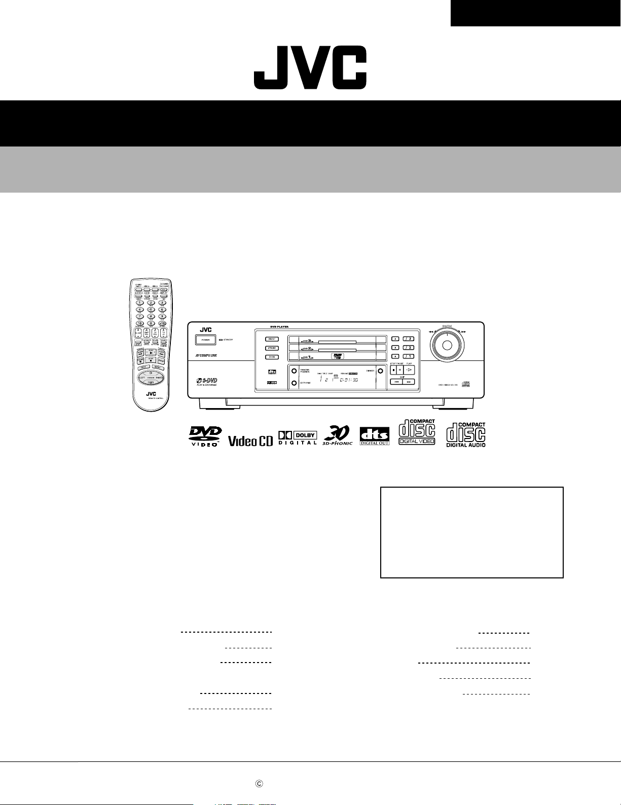
XV-M565BK/M567GDXV-M565BK/M567GD
SERVICE MANUAL
DVD PLAYER
XV-M565BK/M567GD
Contents
Safety precautions
Important for laser products
Preventing static electricity
Dismantling and assembling
the traverse unit
Disassembly method
This service manual is printed on 100% recycled paper.
COPYRIGHT 2000 VICTOR COMPANY OF JAPAN, LTD.
1-2
1-3
1-4
1-5
1-6
Areas suffix
J ----------------------------- U.S.A.
C -------------------------- Canada
Check points for each error
Precautions for service
Troubleshooting
Adjustment method
Description of major ICs
1-21
1-24
1-25
1-31
1-34
No.20845
Jun. 2000
Page 2
XV-M565BK/M567GD
Safety Precautions
1. This design of this product contains special hardware and many circuits and components specially
for safety purposes. For continued protection, no changes should be made to the original design
unless authorized in writing by the manufacturer. Replacement parts must be identical to those
used in the original circuits. Services should be performed by qualified personnel only.
2. Alterations of the design or circuitry of the product should not be made. Any design alterations of
the product should not be made. Any design alterations or additions will void the manufacturer`s
warranty and will further relieve the manufacture of responsibility for personal injury or property
damage resulting therefrom.
3. Many electrical and mechanical parts in the products have special safety-related characteristics.
These characteristics are often not evident from visual inspection nor can the protection afforded
by them necessarily be obtained by using replacement components rated for higher voltage,
wattage, etc. Replacement parts which have these special safety characteristics are identified in
the Parts List of Service Manual. Electrical components having such features are identified by
shading on the schematics and by ( ) on the Parts List in the Service Manual. The use of a
substitute replacement which does not have the same safety characteristics as the recommended
replacement parts shown in the Parts List of Service Manual may create shock, fire, or other
hazards.
4. The leads in the products are routed and dressed with ties, clamps, tubings, barriers and the
like to be separated from live parts, high temperature parts, moving parts and/or sharp edges
for the prevention of electric shock and fire hazard. When service is required, the original lead
routing and dress should be observed, and it should be confirmed that they have been returned
to normal, after re-assembling.
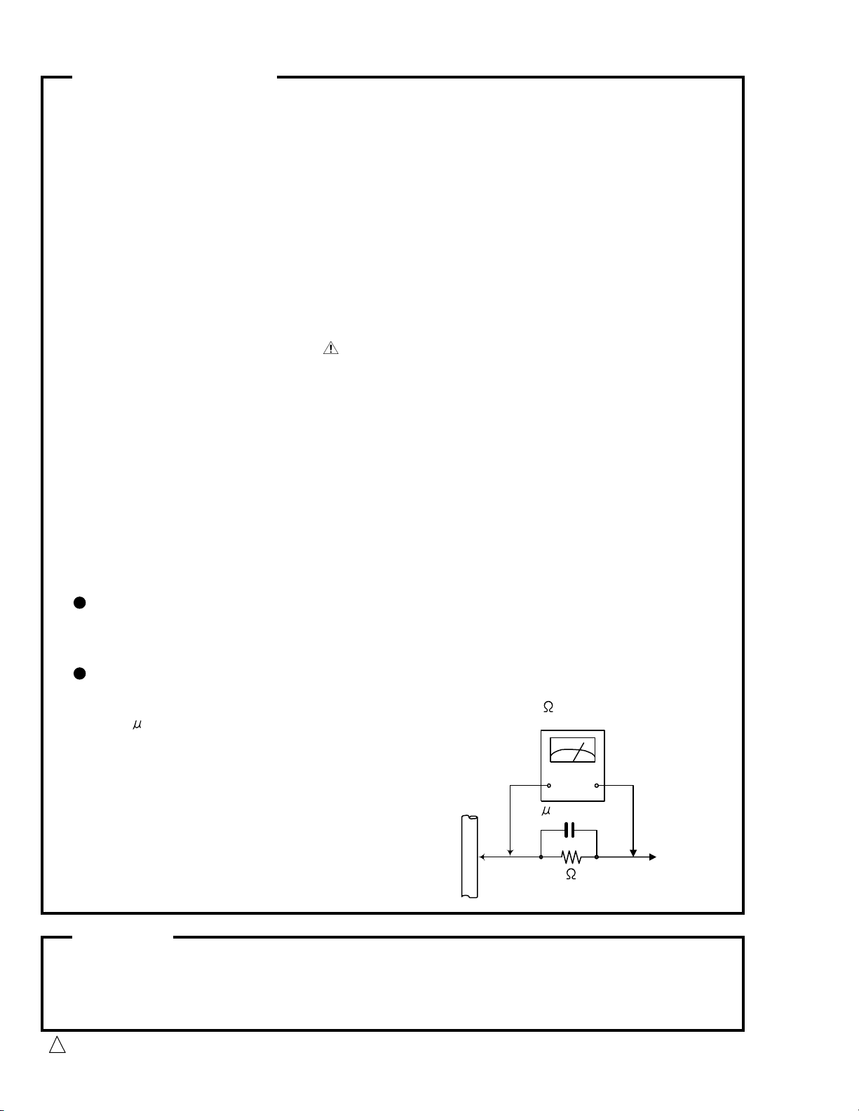
5. Leakage currnet check (Electrical shock hazard testing)
After re-assembling the product, always perform an isolation check on the exposed metal parts
of the product (antenna terminals, knobs, metal cabinet, screw heads, headphone jack, control
shafts, etc.) to be sure the product is safe to operate without danger of electrical shock.
Do not use a line isolation transformer during this check.
Plug the AC line cord directly into the AC outlet. Using a "Leakage Current Tester", measure
the leakage current from each exposed metal parts of the cabinet , particularly any exposed
metal part having a return path to the chassis, to a known good earth ground. Any leakage
current must not exceed 0.5mA AC (r.m.s.)
Alternate check method
Plug the AC line cord directly into the AC outlet. Use an AC voltmeter having, 1,000 ohms
per volt or more sensitivity in the following manner. Connect a 1,500 10W resistor paralleled by
a 0.15 F AC-type capacitor between an exposed
metal part and a known good earth ground.
Measure the AC voltage across the resistor with the
AC voltmeter.
Move the resistor connection to eachexposed metal
part, particularly any exposed metal part having a
return path to the chassis, and meausre the AC
voltage across the resistor. Now, reverse the plug in
the AC outlet and repeat each measurement. voltage
measured Any must not exceed 0.75 V AC (r.m.s.).
This corresponds to 0.5 mA AC (r.m.s.).
0.15 F AC TYPE
1500 10W
Good earth ground
AC VOLTMETER
(Having 1000
ohms/volts,
or more sensitivity)
Place this
probe on
each exposed
metal part.
Warning
1. This equipment has been designed and manufactured to meet international safety standards.
2. It is the legal responsibility of the repairer to ensure that these safety standards are maintained.
3. Repairs must be made in accordance with the relevant safety standards.
4. It is essential that safety critical components are replaced by approved parts.
5. If mains voltage selector is provided, check setting for local voltage.
Burrs formed during molding may be left over on some parts of the chassis. Therefore,
pay attention to such burrs in the case of preforming repair of this system.
1-2
CAUTION
!
Page 3
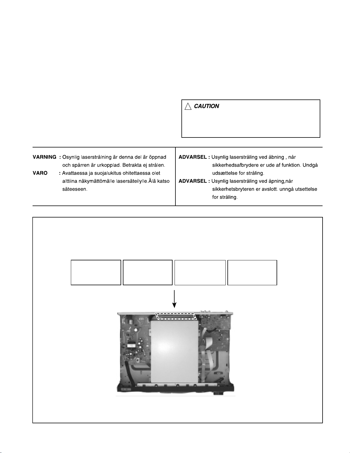
Important for Laser Products
XV-M565BK/M567GD
1.CLASS 1 LASER PRODUCT
2.DANGER : Invisible laser radiation when open and inter
lock failed or defeated. Avoid direct exposure to beam.
3.CAUTION : There are no serviceable parts inside the
Laser Unit. Do not disassemble the Laser Unit. Replace
the complete Laser Unit if it malfunctions.
4.CAUTION : The compact disc player uses invisible
laserradiation and is equipped with safety switches
whichprevent emission of radiation when the drawer is
open and the safety interlocks have failed or are de
feated. It is dangerous to defeat the safety switches.
5.CAUTION : If safety switches malfunction, the laser is able
to function.
6.CAUTION : Use of controls, adjustments or performance of
procedures other than those specified herein may result in
hazardous radiation exposure.
!
Please use enough caution not to
see the beam directly or touch it
in case of an adjustment or operation
check.
REPRODUCTION AND POSITION OF LABELS
WARNING LABEL
DANGER : Invisibie laser radiation
when open and interlock or
defeated.
AVOID DIRECT EXPOSURE TO
BEAM (e)
VARO : Avattaessa ja suojalukitus
ohitettaessa olet alttiina
näkymättömälle lasersäteilylle.Älä
katso säteeseen. (d)
VARNING : Osynlig laserstrålning är
denna del är öppnad och spårren är
urkopplad. Betrakta ej strålen. (s)
ADVARSEL :Usynlig laserstråling
ved åbning , når
sikkerhedsafbrydere er ude af
funktion. Undgå udsættelse for
stråling. (f)
1-3
Page 4
XV-M565BK/M567GD
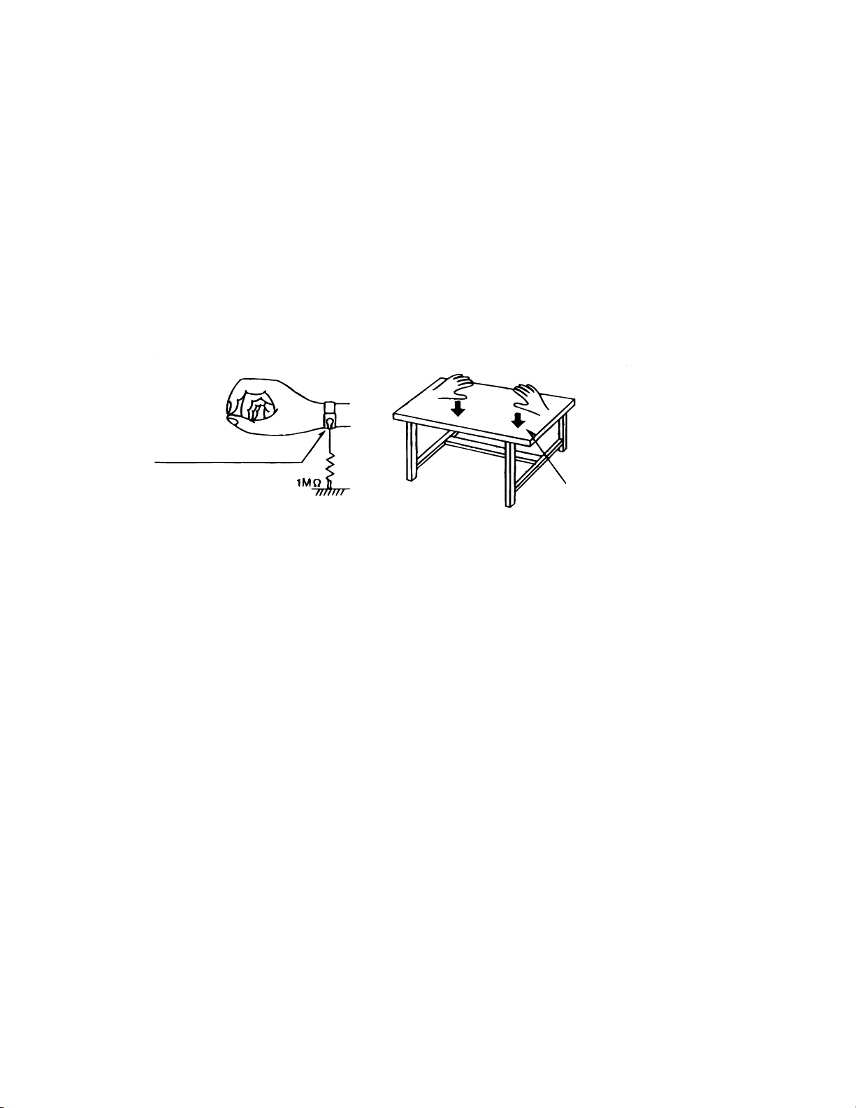
Preventing static electricity
Electrostatic discharge (ESD), which occurs when static electricity stored in the body, fabric, etc. is discharged,
can destroy the laser diode in the traverse unit (optical pickup). Take care to prevent this when performing repairs.
1.1. Grounding to prevent damage by static electricity
Static electricity in the work area can destroy the optical pickup (laser diode) in devices such as DVD players.
Be careful to use proper grounding in the area where repairs are being performed.
1.1.1. Ground the workbench
1. Ground the workbench by laying conductive material (such as a conductive sheet) or an iron plate over
it before placing the traverse unit (optical pickup) on it.
1.1.2. Ground yourself
1. Use an anti-static wrist strap to release any static electricity built up in your body.
(caption)
Anti-static wrist strap
Conductive material
(conductive sheet) or iron plate
1.1.3. Handling the optical pickup
1. In order to maintain quality during transport and before installation, both sides of the laser diode on the
replacement optical pickup are shorted. After replacement, return the shorted parts to their original condition.
(Refer to the text.)
2. Do not use a tester to check the condition of the laser diode in the optical pickup. The tester's internal power
source can easily destroy the laser diode.
1.2. Handling the traverse unit (optical pickup)
1. Do not subject the traverse unit (optical pickup) to strong shocks, as it is a sensitive, complex unit.
2. Cut off the shorted part of the flexible cable using nippers, etc. after replacing the optical pickup. For specific
details, refer to the replacement procedure in the text. Remove the anti-static pin when replacing the traverse
unit. Be careful not to take too long a time when attaching it to the connector.
3. Handle the flexible cable carefully as it may break when subjected to strong force.
4. It is not possible to adjust the semi-fixed resistor that adjusts the laser power. Do not turn it
1-4
Page 5
XV-M565BK/M567GD
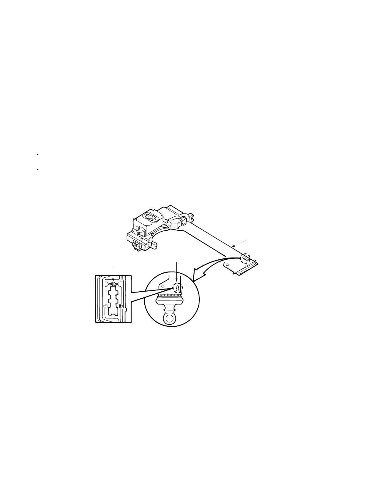
Dismantling and assembling the traverse unit
1. Notice regarding replacement of optical pickup
Electrostatic discharge (ESD), which occurs when static electricity stored in the body, fabric, etc. is discharged,
can destroy the laser diode in the traverse unit (optical pickup). Take care to prevent this when performing
repairs to the optical pickup or connected devices.
(Refer to the section regarding anti-static measures.)
1. Do not touch the area around the laser diode and actuator.
2. Do not check the laser diode using a tester, as the diode may easily be destroyed.
3. It is recommended that you use a grounded soldering iron when shorting or removing the laser diode.
Recommended soldering iron: HAKKO ESD-compatible product
4. Solder the land on the optical pickup's flexible cable.
Note : Short the land after shorting the terminal on the flexible cable using a clip, etc., when using an
ungrounded soldering iron.
Note : After shorting the laser diode according to the procedure above, remove the solder according
to the text explanation.
Short circuit land
Laser pick-up unit
Flexible cable
Shorting
Shot with the rclip
1-5
Page 6
XV-M565BK/M567GD
Disassembly method
<
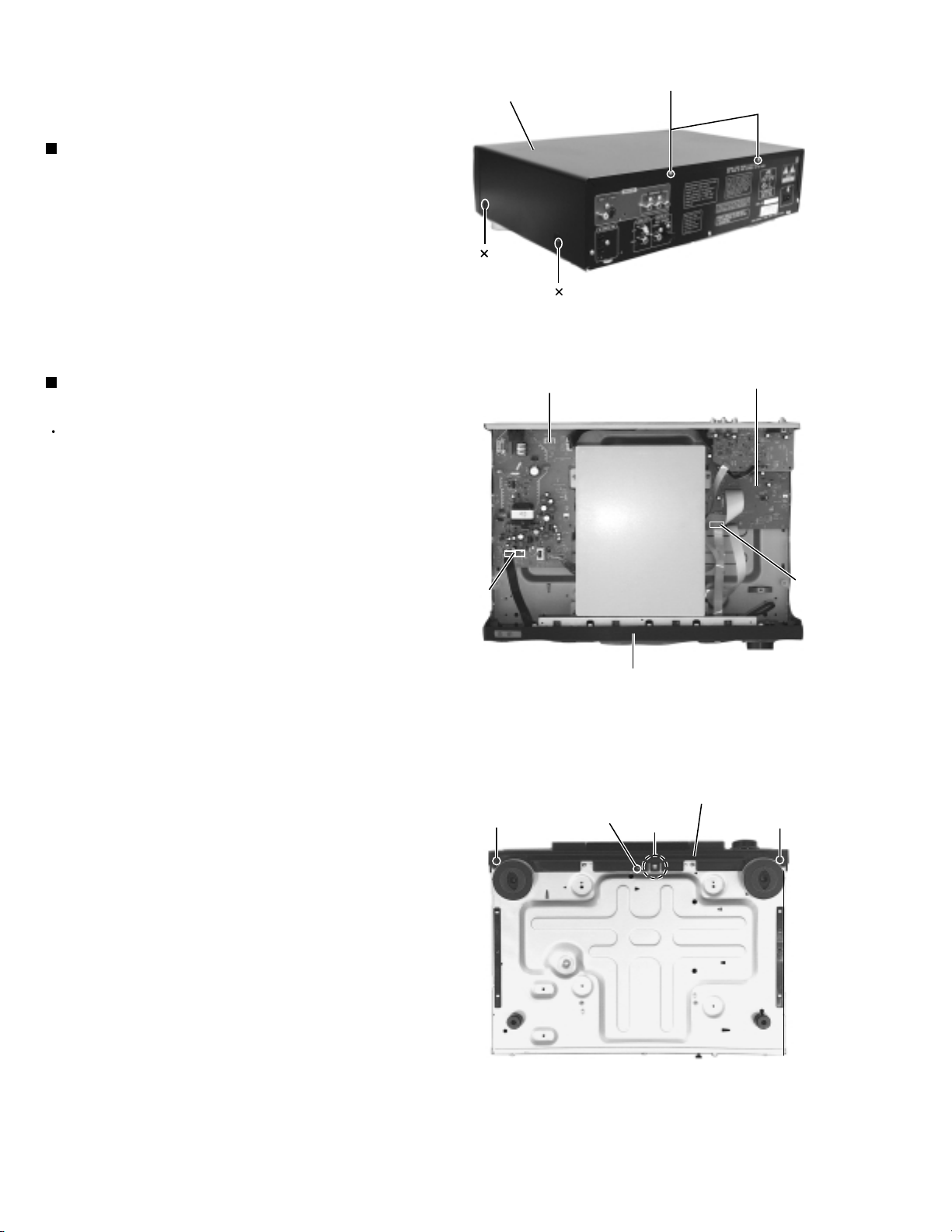
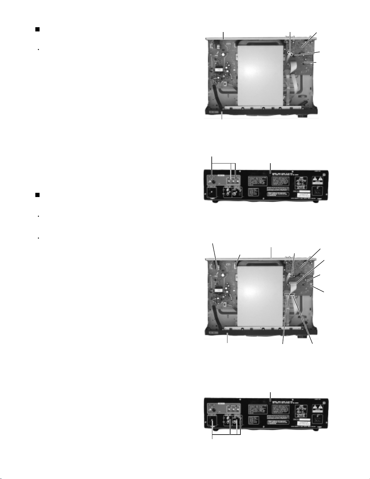
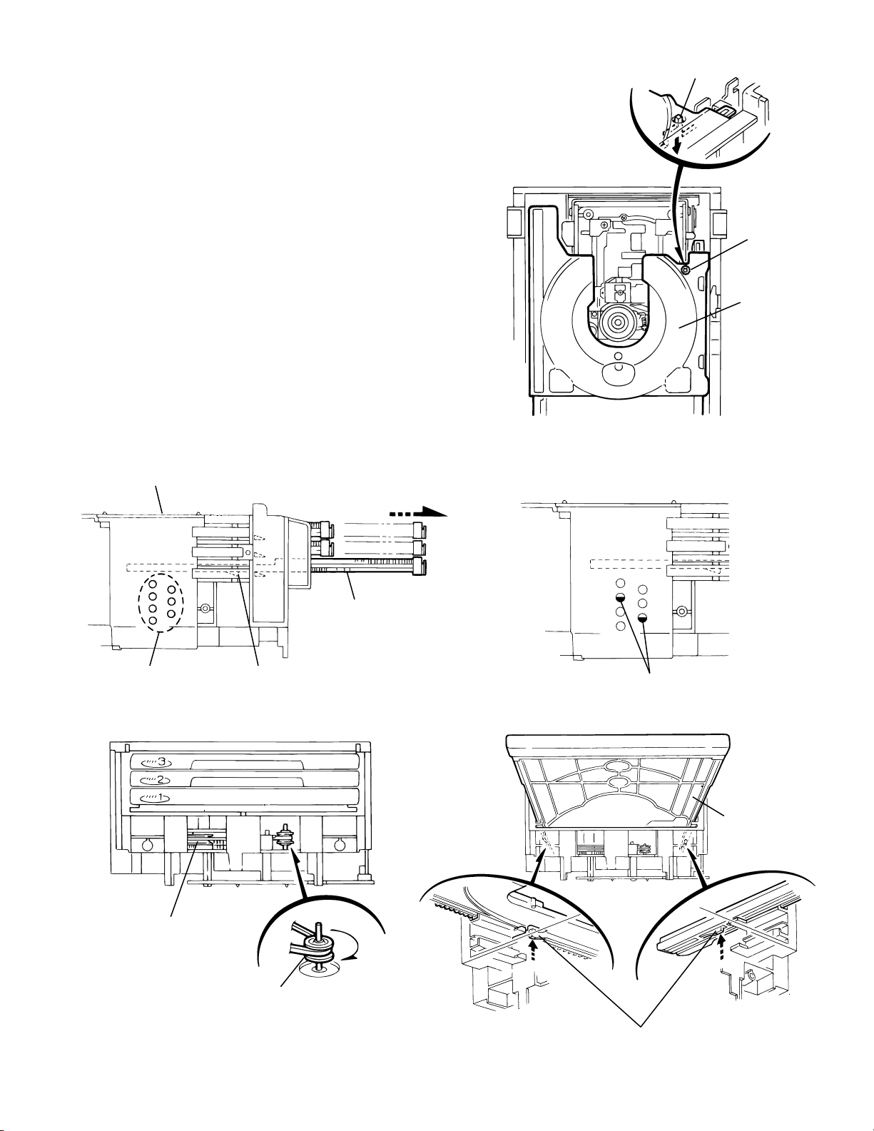
Main body
Removing the Top cover (See Fig.1)
1.
Remove the two screws A attaching the top cover
on the back of the body.
2.
Remove the four screws B attaching the top cover
on both sides of the body.
3.
Pull the lower parts of the top cover sides and
remove the top cover in the direction of the arrow.
Removing the Front panel assembly
Prior to performing the following procedure, remove
the top cover.
1.
Disconnect the harness from connector CN971 and
CN972 on the power supply board.
>
(See Fig.2 to 5)
Top cover
B
2
B
Power supply board
A
2
Fig.1
System control board
2.
Disconnect the card wire from connector CN703 on
the system control board.
3.
Remove the three screws C attaching the front
panel assembly on the bottom of the body.
4.
Release the joint a on the bottom and the two joints
b on both sides of the body. Remove the front panel
assembly toward the front.
CN971
CN972
C
Front panel assembly
Fig.2
Front panel assembly
C
Joint a
CN703
C
1-6
Fig.3
Page 7
Front panel assembly
XV-M565BK/M567GD
Fig.5
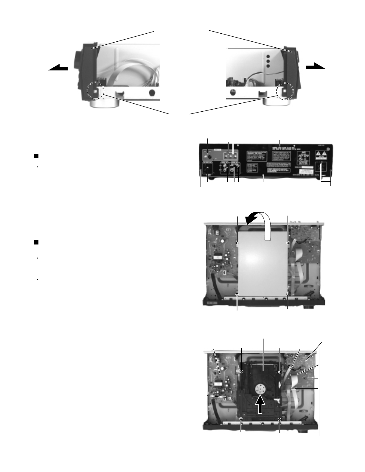
Removing the Rear panel (See Fig.6)
Prior to performing the following procedure, remove
the top cover.
1.
Remove the eleven screws D attaching the rear
panel on the back of the body and detach the rear
panel.
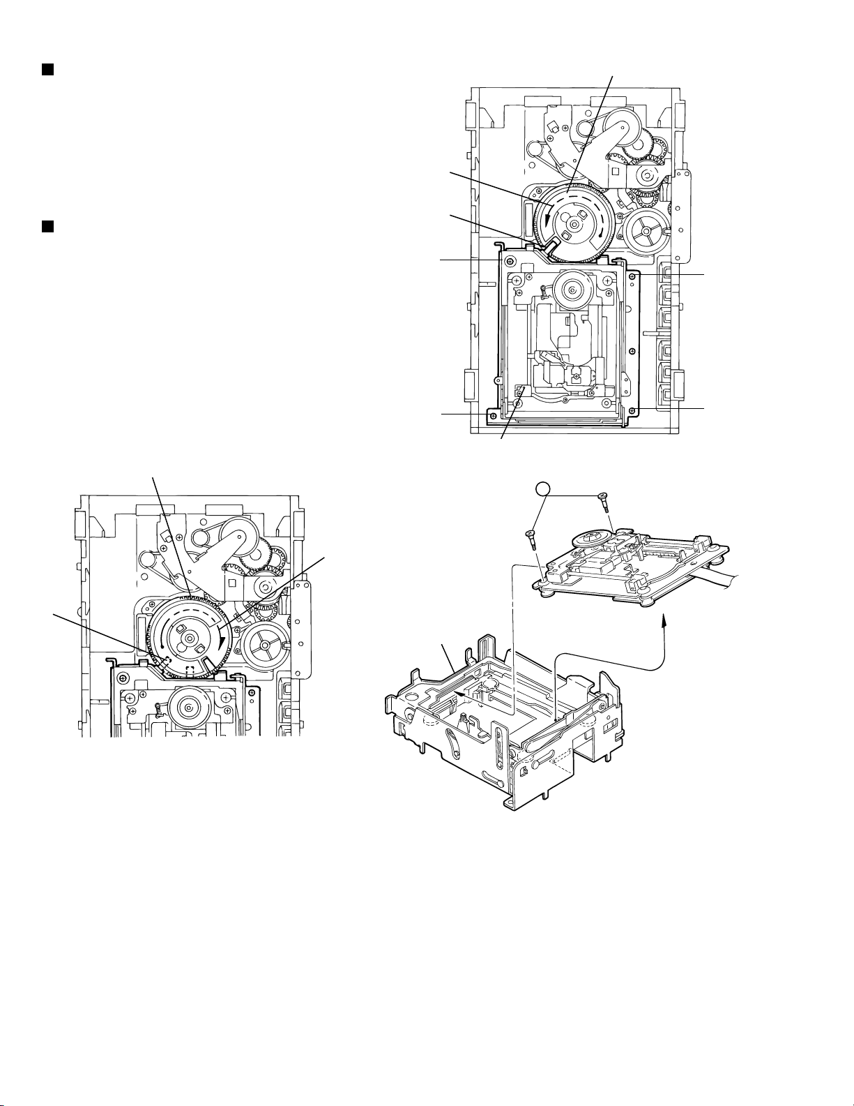
Removing the DVD changer mechanism assembly
(See Fig.7 and 8)
Prior to performing the following procedure, remove
the top cover.
The DVD changer mechanism assembly can be
removed even if the front panel assembly is
attached.
Joints b
D
D
E
Fig.4
Rear panel
Fig.6
Shield case
D
E
1.
Remove the four screws E attaching the DVD
changer mechanism assembly cover and detach the
shield case at an angle.
2.
Disconnect the 9pin harness from connector CN961
on the power supply board.
3.
Disconnect the card wire from connector CN601 on
the video board.
4.
Disconnect the card wires from connector CN701
and CN702 on the system control board.
5.
Remove the four screws F attaching the DVD
changer mechanism assembly. Pull up the DVD
changer mechanism assembly at an angle from the
front panel assembly.
DVD changer mechanism assembly
Power supply board
CN961
E
F
F
Fig.7
Fig.8
F
F
E
Video board
CN601
CN701
System control
board
CN702
1-7
Page 8
XV-M565BK/M567GD
Removing the Power supply board
(See Fig.9 and 10)
Prior to performing the following procedure, remove
the top cover.
1.
Disconnect the harness from connector CN971 and
CN972 on the regulator board (The harness is
extending from the front panel assembly).
2.
Disconnect the 9pin harness from connector CN961
on the power supply board (The harness is
extending from the DVD changer mechanism
assembly).
3.
Disconnect the harness from connector CN951 and
CN952 on the power supply board (The harness is
extending from the system control board).
4.
Remove the screw D attaching the AC jack on the
rear panel.
5.
Remove the two screws G attaching the power
supply board and detach the power supply board.
Power supply board
G
CN971
CN972
CN961
Rear panel
CN951
CN952
Shield case
Rear panel
G
Front panel assembly
Fig.9
Fig.10
D
1-8
Page 9
XV-M565BK/M567GD
Removing the Video board
(See Fig.11 and 12)
Prior to performing the following procedure, remove
the top cover.
1.
Disconnect the card wire from connector CN601 on
the video board (The card wire is extending from the
DVD changer mechanism assembly).
2.
Disconnect the harness from connector CN704 on
the system control board (The harness is extending
from the video board).
3.
Remove the three screws D attaching the video
board on the rear panel. Pull out the video board
from the rear panel.
Removing the System control board
(See Fig.13 and 14)
Prior to performing the following procedure, remove
the top cover.
Rear panel
Front panel assembly
D
Shield case
Fig.11
Rear panel
Fig.12
CN601
Video board
CN704
System
control
board
The audio board can be removed even if the video
board is attached.
1.
Disconnect the card wire from connector CN703 on
the system control board (The card wire is extending
from the front panel assembly).
2.
Disconnect the card wire from connector CN701 and
CN702 on the audio board (The card wires are
extending from the DVD changer mechanism
assembly).
3.
Disconnect the harness from connector CN704 on
the system control board (The harness is extending
from the video board).
4.
Disconnect the harness from connector CN951 and
CN952 on the power supply board (The harness is
extending from the system control board).
5.
Remove the screw H attaching the system control
board.
6.
Remove the five screws D attaching the system
control board on the rear panel. Pull out the system
control board toward the front.
Power supply board
Front panel assembly
CN951
CN952
Shield case
Rear panel
Fig.13
Rear panel
CN704
CN703 CN702
Video board
CN701
System
control
board
H
D
Fig.14
1-9
Page 10
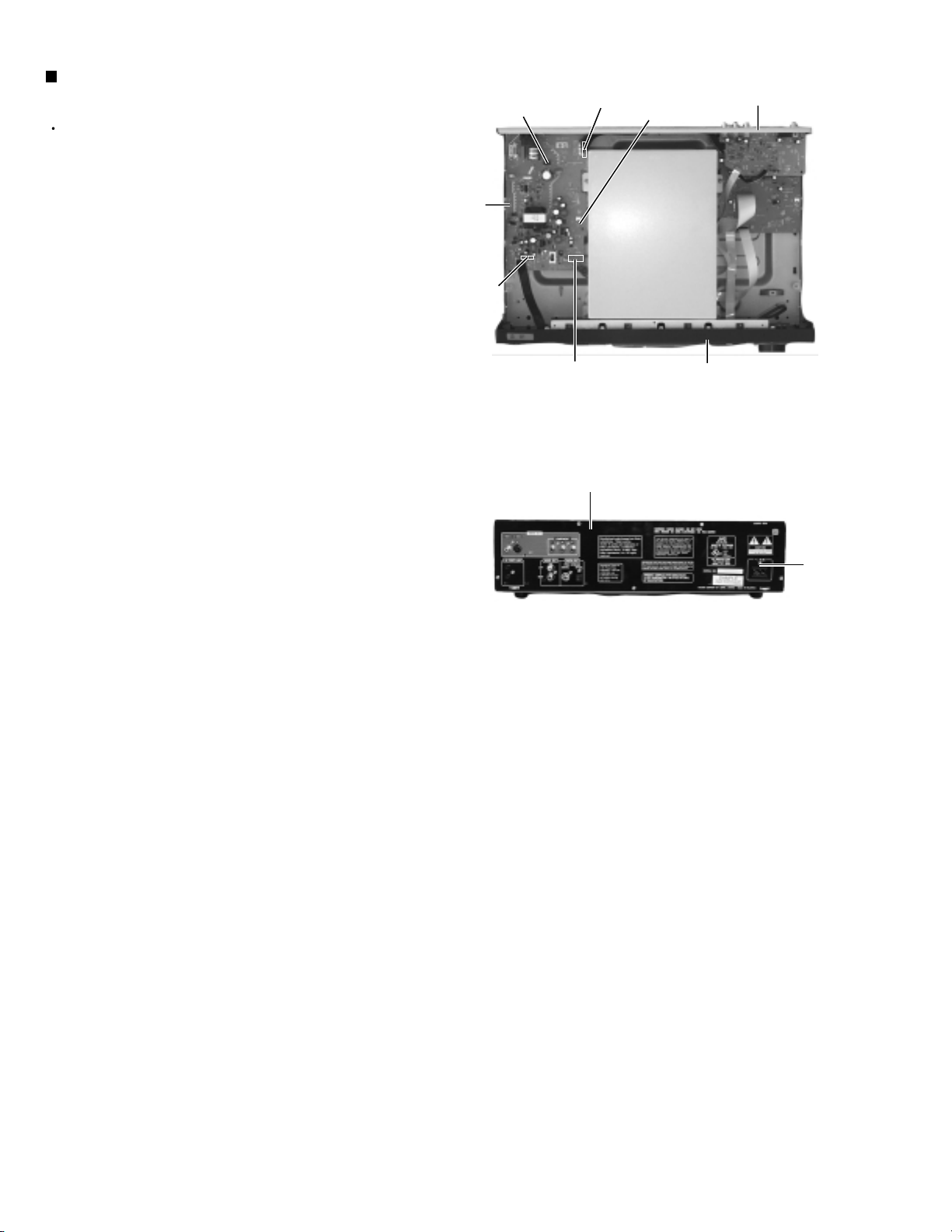
XV-M565BK/M567GD
<
Front panel assembly
Prior to performing the following procedure, remove
the top cover and the front panel assembly.
>
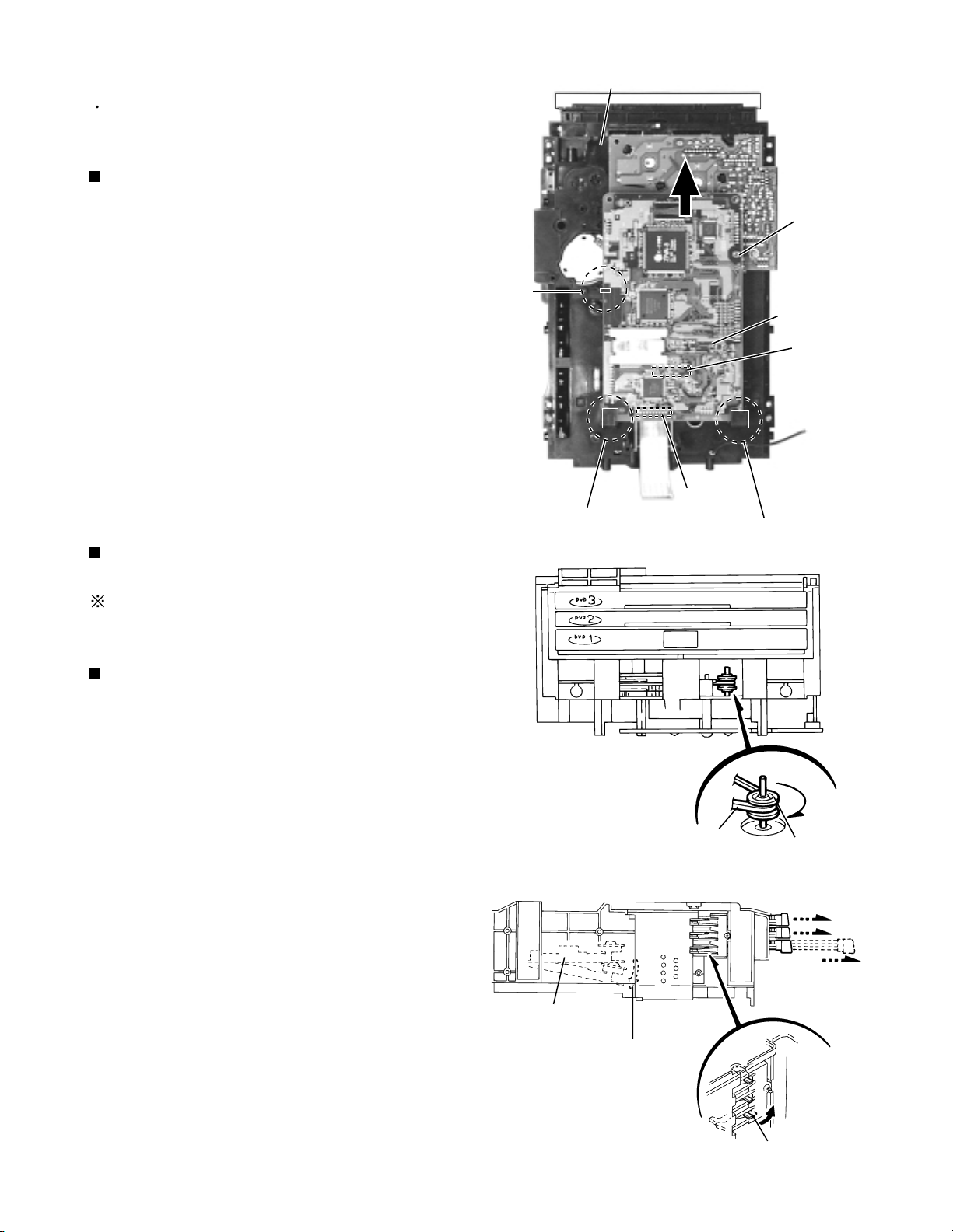
Removing the Front board (See Fig.15)
1.
Remove the four screws I attaching the bracket on
the back of the front panel assembly. Remove the
bracket.
2.
Unsolder the terminal FW802 of the harness
connecting the FL indicator board and the volume
board.
Front panel
assembly
Volume board
I
FW802
I
Bracket
J
J
FL indicator
J
board
Fig.15
J
3.
Remove the eight screws J and the FL indicator
board.
Removing the Volume board
(See Fig.16 and 17)
1.
Pull out the shuttle knob on the front panel
assembly.
2.
Unsolder the terminal FW802 on the back of the
front panel assembly (The harness of FW802 is
connecting the volume board and the FL indicator
board).
3.
Remove the three screws K and the volume board.
Front panel assembly
Shuttle knob
Fig.16
Volume board
FW802
K
1-10
K
Fig.17
Page 11
XV-M565BK/M567GD
<
DVD Changer Mechanism Assembly
Prior to performing the following procedure, remove
the top cover and the DVD changer mechanism
assembly.
>
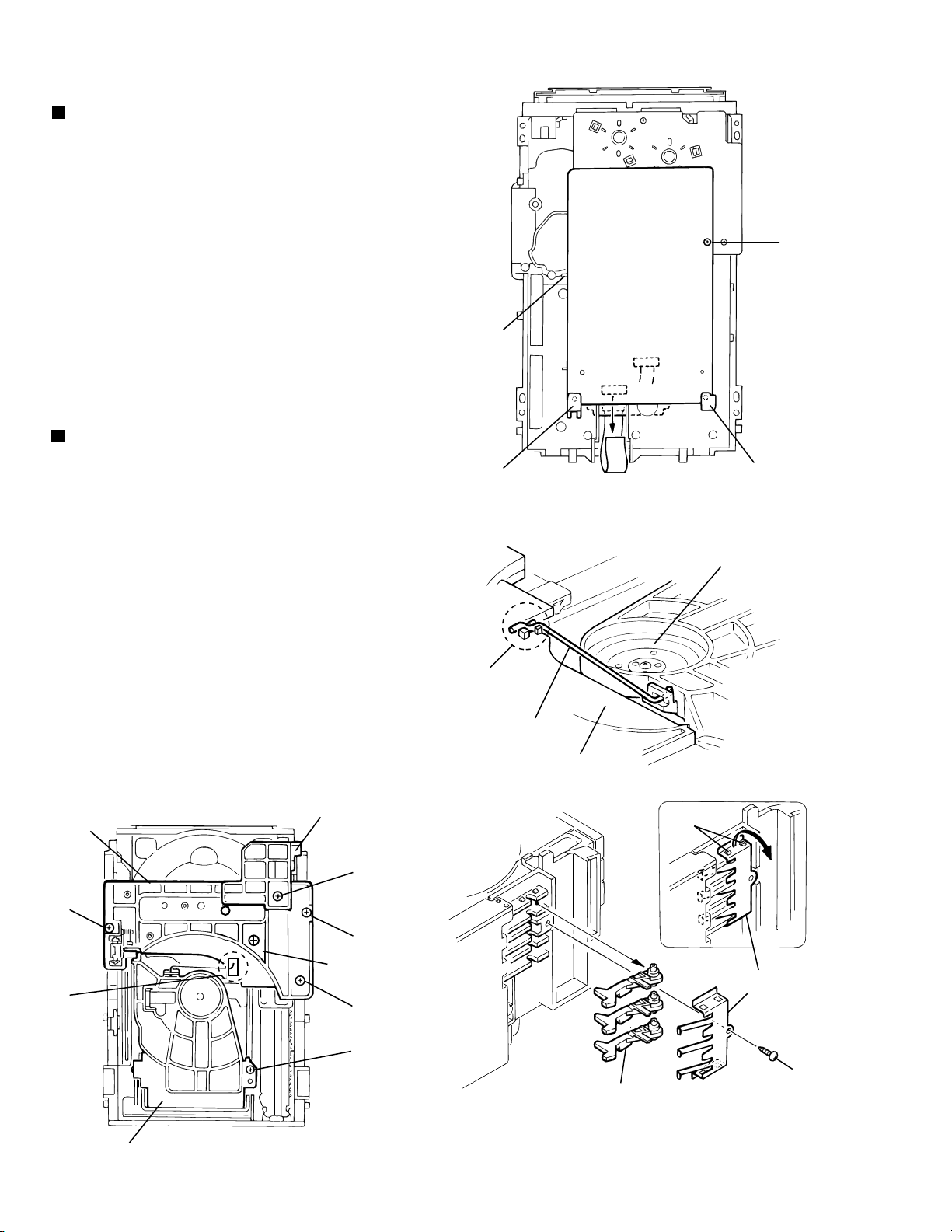
Removing the traverse mechanism
control board (See Fig.18)
1.
Disconnect the card wire from connector CN101 on
the traverse mechanism control board on the bottom
of the DVD changer mechanism assembly.
2.
Remove the screw L attaching the traverse
mechanism control board. Release the three parts e,
f and g and remove the traverse mechanism control
board.
3.
Disconnect the card wire from connector CN102 on
the traverse mechanism control board.
Ejecting the DVD (See Fig.19 and 20)
When the DVD is set or the traverse
mechanism is up.
The DVD tray can not be ejected when the traverse
mechanism is up.
DVD changer mechanism assembly
Par t
e
CN101
Par t
f
Fig.18
DVD traverse
mechanism
control board
Par t
g
L
CN102
Bringing down the traverse mechanism
as shown in the Fig.20
1.
The motor pulley and the belt can be seen on the
front side of the changer. Turn the motor pulley
clockwise until the belt stops.
2.
Pull the tray lock lever on the left side of the changer
and draw the DVD tray.
3.
Draw the DVD tray 1 to 3 as above.
Traverse mechanism
As the motor pulley is
turned, the traverse
mechanism lowers.
Fig.19
Belt
Motor pulley
Draw the DVD tray.
Tray stopper
Fig.20
Tray lock lever
1-11
Page 12
XV-M565BK/M567GD
<
DVD Changer Mechanism Section
Removing the DVD mechanism board
(See Fig.1)
1.
Remove the DVD mechanism assembly cover.
2.
Remove the DVD changer mechanism assembly.
3.
From bottom side the DVD changer mechanism
assembly, remove the one screw A retaining the DVD
traverse mechanism control board.
Disconnect the card wire from the connectors CN101
4.
and CN102 on the DVD traverse mechanism control
board.
Disengage the one engagement a and two
5.
engagements b , remove the DVD traverse mechanism
control board.
Removing the DVD tray assembly
(See Fig.2~4)
Remove the front panel assembly.
1.
Remove the DVD changer mechanism assembly.
2.
Remove the DVD traverse mechanism control board.
3.
Remove the screw B retaining the Disc stopper
4.
(See Fig.3).
Remove the three screws C retaining the T.bracket
5.
(See Fig.3).
From the clamper base section c, remove both of the
6.
edges fixing the rod(See Fig.2 and 3).
Remove the screw D retaining the clamper assembly
7.
(See Fig.3).
From the left side face of the chassis assembly, remove
8.
the one screw E retaining both of the return spring and
lock lever(See Fig. 4).
By removing the pawl at the section d fixing the return
9.
spring, dismount the return spring(See Fig.4).
Remove the three lock levers(See Fig.4).
10.
Disc stopper
T.Bracket
>
A
DVD traverse
mechanism
control baord
a
CN102
CN101
bb
Fig.1
Clamper base
c
Rod
T.Bracket
Fig.2
d
1-12
C
c
Clamper ass'y
Fig.3
B
C
Lod stopper
(C/J version only)
C
D
Return spring
E
Lock lever
Fig.4
Page 13
XV-M565BK/M567GD
11.
Check whether the lifter unit stopper has been caught
into the hole at the section e of DVD tray assembly as
shown in Fig.5.
Make sure that the driver unit elevator is positioned as
12.
shown in Fig.6 from to the second or fifth hole on the
left side face of the DVD Traverse mechanism
assembly.
[Caution]
13.
14.
15.
Chassis assembly
In case the driver unit elevator is not at above
position, set the elevator to the position as
shown in Fig.7 by manually turning the pulley
gear as shown in Fig.8.
Manually turn the motor pulley in the clockwise
direction until the lifter unit stopper is lowered from the
section e of DVD tray assembly(See Fig.8).
Pull out all of the three stages of DVD tray assembly in
the arrow direction f until these stages stop
(See Fig.6).
At the position where the DVD tray assembly has
stoppend, pull out the DVD tray assembly while
pressing the two pawls g and g' on the back side of
DVD tray assembly(See Fig.9). In this case, it is easy
to pull out the assembly when it is pulled out first from
the stage DVD tray assembly.
Fig.5
Stopper
e
DVD tray
assembly
Refer to Fig.7
Pulley gear
Pawl
DVD tray assembly
g
f
Drive unit of elevator
Fig.7Fig.6
DVD tray assembly
Motor pulley
Fig.8
Pawl ,
g
Fig.9
g'
1-13
Page 14
XV-M565BK/M567GD
Removing the DVD mechanism
assembly(See Fig.10)
1.2.While turning the cams R1 and R2 assembly in the
arrow direction h , align the shaft i of the DVD
mechanism assembly to the position shown in Fig.10.
Remove the four screw F retaining the DVD
mechanism assembly.
Removing the DVD mechanism
(See Fig.11 and 12 )
For dismounting only the DVD machanism without
1.
removing the DVD mechanism assembly, align the shaft
j of the DVD mechanism assembly to the position
shown Fig.11 while turning the cam R1 and R2
assembly in the arrow direction k.
Remove the two screws G raising the DVD mechanism
2.
assembly.
Remove the DVD mechanism assembly in the arrow
3.
direction I from the lifter unit (See Fig. 12)
Cam R1, R2 assembly
Cams R1, R2 assembly
Arrow
h
i
F
F
DVD mechanism assembly
G
F
F
Fig.10
DVD mechanism
assembly
Arrow
k
j
Lifter unit
Fig.11
Fig.12
Arrow
l
1-14
Page 15
Removing the mechanism control
board (See Fig.14, 15)
1.
Absord the four soldered positions m of the right and
left motors with a soldering absorber(See Fig.14).
2.
Remove the two screws H retaining the mechanism
control board(See Fig.14).
Remove the two screws I retaining the tray select
3.
switch board(See Fig.15).
Removing the can unit
(See Fig.15 18 )
1.
Remove the CD mechanism assembly.
2.
While turning the cam gear L, align the pawl n position
of the drive unit to the notch position(Fig.15) on the cam
gear L.
Pull out the drive unit and cylinder gear(See Fig.17).
3.
While turning the cam gear L, align the pawl o position
4.
of the select lever to the notch position(Fig.18) on the
cam gear L.
Remove the four screws J retaining the cam unit(cam
5.
gear L and cams R1/R2 assembly)(See Fig.18).
m
Motor L
Mechanism control board
H
Fig.14
XV-M565BK/M567GD
Motor R
m
H
Chassis assembly
CN801
Fig.15
CN802
Drive unit
CD Tray
switch board
Cylinder gear
CN804
Drive unit
n
I
Cam gear L
J
Cam gear L
Fig.16
Cams R1, R2 assembly
J
Cam unit
J
Fig.17
o
Select lever
Fig.18
1-15
Page 16
XV-M565BK/M567GD
Removing the actuator motor and belt
(See Fig.19 22)
1.
Remove the two screws K retaining the gear bracket
(See Fig.19).
2.
While pressing the pawl p fixing the gear bracket in the
arrow direction, remove the gear bracket
(See Fig.19).
From the notch q section on the chassis assembly fixing
3.
the edge of gear bracket, remove and take out the gear
bracket(See Fig. 20).
Remove the belts respectively from the right and left
4.
actuator motor pulleys and pulley gears(See Fig. 19).
After turning over the chassis assembly, remove the
5.
actuator motor while spreading the four pawls r fixing
the right and left actuator motors in the arrow
direction(See Fig. 21).
[Note]
When the chassis assembly is turned over under
the conditions wherein the gear bracket and belt
have been removed, then the pulley gear as well
as the gear, etc. constituting the gear unit can
possibly be separated to pieces. In such a case,
assemble these parts by referring to the assembly
and configuration diagram in Fig. 22.
Pulley gear
Gear bracket
Belt
Motor pulley
K
Fig.19
Actuator motor
Pulley gear
Belt
Motor pulley
K
Pawl
p
Chassis assembly
q
Gear bracket
Fig.20
Assembly and Configuration Diagram
Pulley gear
r
r
Fig.21
Pulley gear
Gear B
Cylinder gear
1-16
Gear B
Gear C
Select gear
Gross gear L
Fig.22
Gross gear U
Gear C
Page 17
XV-M565BK/M567GD
Removing the cams R1/R2 assembly
and cam gear L (See Fig.23)
Remove the slit washer fixing the cams R1 and R2
1.
assembly.
By removing the two pawls s fixing the cam R1,
2.
separate R2 from R1.
Remove the slit washer fixing the cam gear L.
3.
Pull out the cam gear L from the C.G. base assembly.
4.
Removing the C.G. base assembly
(See Fig.23 and 24)
Remove the three screws L retaining the C.G. base
assembly.
[Caution]
To reassemble the cylinder gear, etc.with the
R1/R2
cam unit (cam gear and cams
gear unit and drive unit, align the position of the
pawl n on the drive unit to that of the notch on
the cam gear L. Then, make sure that the gear
unit is engaged by turning the cam gear L
(See Fig. 24).
assembly),
Slit washer
Cam gear L
L
Slit washer
Cam R2
s
Pawl
Cam R1
Cam switch board
C.G. base assembly
Pawl
s
Notch
Pawl
n
Cylinder
gear
Drive unit
Fig.23
Cam gear L
Cam R1, R2 assembly
Gear unit
Gear bracket
Fig.24
1-17
Page 18
XV-M565BK/M567GD
<Traverse mechanism section>
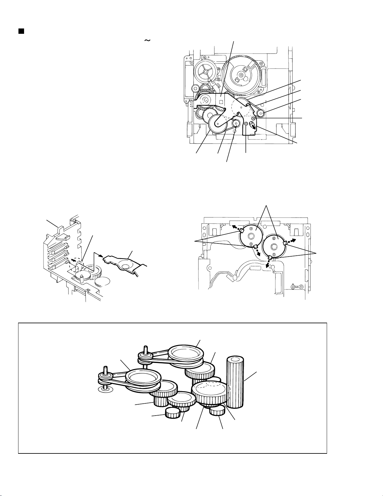
Removing the pickup unit
(See Fig.1 to 3)
1.
Make sure to solder the flexible harness.(In case of
replacement with a new product, unsolder the
flexible harness after performing the following
procedure.)
2.
Disconnect the flexible harness from connector
CN12 on the connection board.
3.
The rack cover is attached to the feed drive shaft.
Remove the two screws A attaching the connection
board and stand the connection board. Remove the
rack cover.
4.
Remove the screw B attaching the pickup shaft
holder. Remove the pickup shaft holder by releasing
ATTENTION:
5.
Pull out the shaft in the direction of the arrow and
slightly lift it with the pickup unit. Then, remove the
pickup unit while pulling the rack a in the direction of
the arrow.
Be careful not to lose the inside spring.
Connection board
A
CN12
Feed drive shaft
A
CN12
Fig.1
Rack cover
Flexible harness
Soldering
(Short circuit round)
Connection board
1-18
Pickup unit
Rack a
Fig.2
Pickup shaft holder
Shaft
Fig.3
Tab
B
Tab
Page 19
XV-M565BK/M567GD
Removing the Spindle Motor Assembly
(See Fig.4 to 8)
1.
Unsolder the two parts b on the connection board.
2.
Remove the screw C attaching the sensor holder
and detach the sensor holder from the turn table
bracket. Slacken and remove the flexible harness of
the part c as shown in Fig.6. Pull up the hook d and
remove the flexible harness from the sensor holder.
(When reattaching the sensor holder)
Let the flexible harness through the part c of the
sensor holder and reattach it to the hook d
correctly (See Fig.6).
Reattach the pin e of the sensor holder to the
notch of the radial lever and reattach the sensor
holder to the turn table bracket.
3.
Remove the three screws D attaching the spindle
motor assembly.
4.
Release the tab by moving the spindle motor
assembly to the tab, and remove the spindle motor
assembly.
Sensor holder
*Part b - soldering
Fig.4
C
Spindle motor
ATTENTION:
D
Do not lose the spring of the shaft f by
the tab.
It is not necessary to remove
at the spindle motor unit exchange.
Turn table bracket
Fig.5
Hook d
Sensor holder
Flexible harness
Part c
Fig.6
D
Tab
f
Pin e
Radial lever
Fig.7Fig.8
1-19
Page 20
XV-M565BK/M567GD
Removing the connection board
(See Fig.9)
1.
Disconnect the flexible harness from connector
CN12 and CN13 on the connection board on the
under side of the chassis.
2.
Unsolder the two parts b (the red and black wires
extending from the spindle motor) on the connection
board.
3.
Remove the two screws A attaching the connection
board and detach the relay board.
Removing the feed motor assembly
(See Fig.10)
A
Part b -soldering
CN12
Feed motor assembly
Fig.9
E
CN13
Spindle motor
g
Prior to performing the following procedure, remove
the connection board.
1.
Unsolder the flexible harness g of the feed motor.
2.
Remove the two screws E attaching the feed motor
assembly and detach the feed motor assembly.
Fig.10
1-20
Page 21

Check points for each error
(1) Spindle start error
*Defective spindle motor
Does the resistance between pins nos. 5 and 7 of CN102 register 6 to 10 ?
(The power supply is turned off and measured.)
*Hall element: Is square wave output with the voltage of CN102 pin no. 2 during rotation?
In either case, replace the mechanical unit.
*Defective BTL driver (IC271)
Is there a voltage output between pins nos. 5 and 7 of CN101?
Is IC271 "25" at "H" level (START)?
Servo IC --- Is control signal sent to the motor driver ?
IC201 "120,121" : Duty is 50% during stop, but varies during rotation (greatly varies at start).
--- If not sent, pattern or servo IC (IC201) is defective.
Is FG input to servo IC ?
Observe FG wave from IC271 "41". --- If not output, pattern, IC271 or IC201 is defective.
XV-M565BK/M567GD
(2) Disc Detection, Distinction error (no disc, no REFNV)
* Laser is defective.
* Front End Processor is defective (IC101).
* APC circuit is defective. --- Q101.
* Pattern is defective. --- Lines for CN101 "2,4,6" and "14".
Lines for between IC201 "2" and IC101 "2"(LDONA),
between IC201 "3" and IC101 "1" (LDONB).
* Servo IC is defective (IC201).
* Does signal flow to IC 101 pin no. 79 and output to (RFINP)?
* IC101 --- For signal from IC101 to IC301, is signal output from IC101 "88" (TS1),
IC101 "69" (RFENV) and IC101 "90" (FS)?
(3) Traverse movement NG
* Traverse motor is defective.
Is there a voltage output between "1" to "6" and "3" to "4" of CN102?
* BTL driver is defective.
Is there a voltage output at Pins nos. "12,13,14" and "15" of IC271?
The voltage of the MUTE2 terminal pin no. "25" of IC271 becomes (H).
Is the driving voltage output on pin nos. "104" and "105" of the servo IC?
--- The servo IC defective or the patterns are incorrect.
1-21
Page 22

XV-M565BK/M567GD
(4) Focus ON NG
* Is FE output ? --- Pattern, IC101
* Is FODRV signal sent ? (R288) --- Pattern, IC201
* Is driving voltage sent ?
CN102 "9", "11" --- If NG, pattern, driver, mechanical unit (with the power turned off, measure the
resistance between CN102 "9" and "11").
* Does CN101 "14"(SRF1) become "H" and is the focus drawing in done?
--- Mechanical unit (laser power too low), IC101(defective gain)
--- Moreover, It is thought that abnormality is found in the disk.
* Mechanical unit is defective.
(5) Tracking ON NG
* When the tracking loop cannot be drawn in, IC201 "58" (/TRON) does not become "L".
* Mechanical unit is defective.
Because the undermentioned adjustment value is abnormal, it is not possible to draw in normally.
* Periphery of driver (IC271)
Constant or IC it self is defective.
(When passing without becoming abnormal while adjusting the following.)
* Servo IC (IC201)
When improperly adjusted due to defective IC.
[Focus position rough adjustment]
[Phase difference cancellation rough adjustment]
[Tracking balance adjustment]
(6) Spindle CLV NG
* When the spindle cannot be shifted to CLV Servo, does not become "H" between IC301 "88"
and IC201"18".
* IC101 Is signal output from CN104 "1" (RFOP)?
* IC101 Is signal output from CN104 "12" (FLTOUT)?
* IC101 Is signal output from CN104 "7" "8" "9" "10" (binary-coded clock and data)?
* IC201 Is "58" (/TRON) at "L" level ?
* Besides the causes mentioned below, it is difficult to point out a specific one because there are various
factors that should be considered.
Mechanism is defective.(jitter)
IC101, IC201.
(7) Address read NG
* Besides the causes mentioned below, it is difficult to point out a specific one because there are various
factors that should be considered.
Mechanism is defective. (jitter)
IC201, IC301, IC401.
The disc is dirty or the wound has adhered.
(8) Between layers jump NG (double-layer disc only)
* Defective mechanism
* The ICs surrounding the driver IC (IC271) are defective.
* Servo IC (IC201) is defective.
1-22
Page 23

(9) Neither picture nor sound is output
* Cannot search
a) Can the feed system be driven?
TRSDRVA and TRSDRVB line signal
Check the voltage of IC201 between pin no. 104 and R273 and pin no. 105 and R277.
After checking the voltage of the driver (IC271) pin nos. 9,10,12 and 13, check the signals
of FMA+, FMA-, FMB+ and FMB-.
b) Is kick available?
Check the TRDRV signal waveform from R285.
Check the waveform of CN102 "8" and "10" --- After the driver (IC271)
(10) Picture is distorted or abnormal sound occurs at intervals of several seconds.
Some system other
Does JITOUT(IC101"64")
change periodically?
NO
than servo may be
defective.
XV-M565BK/M567GD
YES
If this voltage is too
high, feed motor
may be defective, or
the mechanical unit
has seized.
(11) Others (unusual events experienced to date)
* Problem occurs with double-layer discs although no problem occurs with single-layer DVD.
(Error occurs, or search becomes unstable and takes longer.)
Crosstalk might occur from tracking to focus system.
--- When FE was observed during search (skip, etc.), it was found that a wave resembling TE
with an amplitude of 200mVp-p was riding on FE.
--- Mechanical unit was replaced.
* Error frequently occurred in the outer part of discs although no error occurred in the inner part.
--- Mechanical unit was replaced because tilt seemed to be defective.
(12) CD During normal playback operation
a) Is TOC reading normal?
NO
Please refer to "Servo Volume" flow.
Displays total time
for CD-DA.
Shifts to double-speed
mode for V-CD.
YES
b)Playback possible?
NO
*The OSD screen remains on the "No reading" display.
According to [*Cannot serch ] for DVD(9), check the feed
and tracking systems.
*No sound is output although the time is displayed.(CA-DA)
DAC, etc, other than servo.
*The passage of time is not stable, or picture is abnormal.(V-CD)
The wound of the disc and dirt are confirmed.
1-23
Page 24

XV-M565BK/M567GD
Precautions for service
Handling of Traverse Unit and Laser Pickup
1. Do not touch any peripheral element of the pickup or the actuator.
2. The traverse unit and the pickup are precision devices and therefore must not be subjected to
strong shock.
3. Do not use a tester to examine the laser diode. (The diode can easily be destroyed by the
internal power supply of the tester.)
4. To replace the traverse unit, pull out the metal short pin for protection from charging.
5. When replacing the pickup, after mounting a new pickup, remove the solder on the short land
which is provided at the center of the flexible wire to open the circuit.
6. Half-fixed resistors for laser power adjustment are adjusted in pairs at shipment to match the
characteristics of the optical block.
Do not change the setting of these half-fixed resistors for laser power adjustment.
Destruction of Traverse Unit and Laser Pickup by Static Electricity
Laser diodes are easily destroyed by static electricity charged on clothing
or the human body. Before repairing peripheral elements of the traverse
unit or pickup, be sure to take the following electrostatic protection:
1. Wear an antistatic wrist wrap.
2. With a conductive sheet or a steel plate on the workbench on which
the traverse unit or the pick up is to be repaired, ground the sheet
or the plate.
3. When removing the pickup wire, short-circuit the land provided at the center of the pickup flexible wire.
But before carrying out the above, short-circuit the land of the mechanism relay board first.
4. Short-circuit the laser diode by soldering the land which is provided
at the center of the flexible wire for the pickup.
After completing the repair, remove the solder
to open the circuit.
Short-circuit
1-24
Page 25

Troubleshooting
XV-M565BK/M567GD
1.Power-on processing
Does
to
Micro-
computer
Volume.
NO
the lamp
goes out when
POWER switch of
remote control
box is turned
ON?
YES
Check S801
(power switch)
and the line
to IC701.
Power-on
processing is OK.
to Power Supply
Volume.
Connect to outlet.
STANDBY
indicating lamp
Press POWER switch.
NO
indicating lamp
YES
NO
voltage applied at each
lights up?
YES
STANDBY
goes out?
Does FL
light up?
NO
Correct
lead
of FL?
YES
A
NO YES
fuse is blown
Voltage of
IC953"1" at
approx.9.0V
YES
B
F901
NO
YES
AC 1.4V) come out to
Replace
NO
wave detected on
the anode side of
Does the
oscillation wave
come out to
IC901"4"
NO
Does the
DC voltage(input
D901 output side
NO
Replace
D901.
Return to A
and recheck.
F901.
Is the AC
D954
NO
YES
YES
Return to A
and recheck.
YES
Connecting wires
to the soldered
part of the pins of
T901(transformer)
and anode of D904
is examined.
Replace
Return to A
and recheck.
Is energizing
of "cathode of D954"
and "pin1 of IC953"
YES
Replace
D954.
Return to A
and recheck.
IC901.
normal?
NO
Repair the
wiring.
Return to A
and recheck.
Return to A
and recheck.
to Power Supply
Return to B
and recheck.
Repair the wiring.
To Microcomputer
Volume.
Volume.
Check
IC802,C814
between IC802"5"
and IC701"49" OK?
NO
NO
NO
Is connection
YES
Voltage
of CN971"5"
at +5V?
YES
Replace IC802.
Return to B
and recheck
Correct voltage
applied to IC802
(FL driver)?
YES
Oscillating
wave output from
IC802"2"
YES
NONO
of IC802"12-15" and
IC701"45-48" OK?
To Microcomputer Volume.
of IC953"3"
computer
Voltage
of IC802"5"
(P.ON RESET)
at +5V?
YES
Is connection
YES
Voltage
at 5 V?
to
Micro-
Volume.
YES
NO
NO
OK between IC953"3"
Repair the
wiring.
Return to B
and recheck.
Is IC953
hot?
YES
Continuity
and IC701"11,100"
OK
To Microcomputer
Volume.
NO
NG
Replace
IC953.
Return to A
and recheck.
Repair the
wiring.
Return to A
and recheck.
1-25
Page 26

XV-M565BK/M567GD
2. Power Supply Volume
With all the wiring removed, check unit power board.
(1) Remove all flat wires and wire assemblies which are connected to CN971,CN972,CN951,CN952,CN981.
(2) Short -circuit CN951 "1" (POWER ON:B9006) and "2" (B5V:B9019). (Set each regulator to ON.)
(3)
The load resistance is connected between CN961 "4" (D5V:B9008) and "3,4"(D.GND:B9001).
(4) Connect to the outlet and check the voltage at each part.
(For the voltage specification, see the standard schematic diagrams.)
* If the load resistance is not connected, the voltage is not output to "B9008".
Then restore the connection of CN971,CN972,CN951,CN952,CN981 and check voltage.
(1) Remove the wire short -circuiting CN951 "1" and "2".
(2) Remove the load resistance.
(3) Restore the connection of CN971,CN972,CN951,CN952,CN981.
(4) Connect to the outlet.
(5) Turn the POWER switch on and check the voltage at each part.
If voltage abnormally drops when CN971,CN972,CN951,CN952,CN981 are connected (load is connected)
though the voltage was at the normal level when CN971,CN972,CN951,CN952,CN981 were disconnected
(load is connected), or if the protective element (fuse, etc.) is opened, the load which is supplied power may
be defective or the wiring may be short-circuited.
3. Open/Close Operation
Press OPEN/CLOSE key
Does the tray
smoothly open?
YES
OPEN/CLOSE
operation is OK.
Check S821-S823
and thewiring to IC802.
the remote control
(OPEN/CLOSE)
YES
of
box functions
normally?
NONO
To Microcomputer
Volume.
NO
Voltage
of IC701"27"
at 0V?
YES
Check the
connection
between CN702
and mechanical
unit. Check the
mechanical unit.
1-26
Page 27

4. Microcomputer Volume
Processing of Each Microcomputer
* IC701 System microcomputer (sub-microcomputer)
After powering on, this microcomputer is continuously activated to control keys and remote control
signals.
According to key operations or remote control signals, it controls (turns on/off) the power for
LSIs including IC401 (main microcomputer) and the audio/video output circuit.
It also controls the resetting of the main microcomputer, FL driver IC (IC802) for FL display.
IC401 Main microcomputer
*
This microcomputer controls a group of LSIs of servo and signal processing sections according to
commands from the system microcomputer.
After receiving time information from the signal processing section, it transmits the information
together with the status to the system microcomputer.
It controls the resetting of the LSIs of the servo and signal processing sections.
It has IC402 (16Mbit ROM) as an external ROM.
XV-M565BK/M567GD
Normal Starting Conditions
* IC701 System microcomputer
(1) +5V must be applied to "11" and "100".
(2) Oscillators of "12" and "13" must be oscillating correctly.
(3) Input to "33" (RESET) must be at +5V (reset cancel).
If above (1) to (3) are not satisfied when the STANDBY indicating lamp does not light at
power-on, IC701 may be defective.
* IC401 Main microcomputer
(1) +5V must be applied to "17","22","34","54","66","83"
(2) Clock signal (13.5MHz) must be input to "23".
(3) Input to "82" (RST) must be at +5V (reset cancel).
(4) Communication line with IC701 ("57","58,"67"~"69") and that with IC402 (external ROM)
("13"~"16","26"~"33","35"~"42","44","93"~"100") must work normally.
If above (1) to (3) are not satisfied when the STANDBY indicating lamp goes out but FL does not
light when the POWER switch is turned on, IC401, IC701 or IC402 may be defective.
1-27
Page 28

XV-M565BK/M567GD
5. Audio Volume
Is
digital signal
input to
IC703"2"?
YES
YES
OK
NO
Check IC703
and PLL.
Power
supplied correctly
to each IC?
YES
Is sound
signal output
from J701 (pin
jack)?
NO
Voltage of
Q791 collector at
-5.5V?
YES
* Changing over the cutoff frequency of analog LPF
NO
to Power Supply
Volume
NO
IC701 is
checked
When fs=44.1kHz or 48kHz,
Microcomputer port FS2 is at the "L" level,
and Q741 and Q751 are turned ON.
Is digital
signal output from
IC703"10", "13", "16"
and "19"?
YES
Check IC751, IC741
and their periphery.
NO
Replace
IC703.
When fs=96kHz,
Microcomputer port FS2 is at the "H" level,
and Q741 and Q751 are turned OFF.
1-28
Page 29

6. Video Volume
XV-M565BK/M567GD
Power
supplied correctly
to each IC?
YES
Is video
signal output from
J602 S terminal?
NO
Is signal
output from CN601
"1","3","5"
"7","9"?
YES
Check the
peripheral circuit
NO
YES
NO
to Power Supply
Volume
Is video
signal output from
J602 composite
terminal?
OK
* +5V power for video section is
NO
YES
Is clock
signal input to
IC554"29"?
Is digital
signal output from
IC554"39" to"46", "49"
and"50"?
supplied from IC554.
Check I/O voltage of IC554.
Check the insertion of
CN601
NO
YES
YES
NO
Check
IC501.
Check
IC501.
Signal flow of DISC media
DISC
IC101
FEP
IC301
ODC
IC501
AV DEC.
Check
IC554.
VIDEO
CIRCUIT
IC703
DAC
VIDEO
LPF
AUDIO
1-29
Page 30

XV-M565BK/M567GD
7.Servo volume
Press
key
Does the tray
operates
normally?
Y
N
to
3. Open/Close Operation
Section
from A
Is the jump between
layers OK?
FE
*only two layer
disc (DVD)
N
to
(8) Between layers jump
NG Section
Does the pickup
lens moves up
and down?
Y
Does the FL
display register
"NO DISC"?
Y
Is the disc
rotating?
Y
Is drawing in
FOCUS normal ?
FE
OFF
ON
(It is NG when
tick tack retrying.)
Y
Is drawing in
TRACKING normal ?
to
N
(3) Traverse movement
NG Section
to
Y
(2) Disc Detection, Distinction
error Section
to
N
(1)Spindle start error Section
N
to
(4) Focus ON NG Section
LO LI
Y
Was information on
the disc obtained?
(In case of NG,
perform the disc
changing or enter
the stop mode.)
Y
Can you reproduce ?
Y
OK !
to
N
(7) Address read NG
Section
N
(9) Checkpoint
according to error
TE
OFF
ON
Does IC201"58"
(/TRON) become "L" ?
Y
Is the shift to
spindle CLV OK ?
Does IC201"18"
(PLLOK) become "H" ?
Y
to A
1-30
N
to
(5) Tracking ON NG Section
N
to
(6)Spindle CLV NG Section
Page 31

Adjustment method
Jig for adjustment:
Stud bolt (4 pc.) .................... Parts No. JIGXVM555-KIT 1 set
Hexagonal wrench for adjustment ........................................ 1 pc.
Extension cable
Terminal 19 (CN10) Parts No. QUQ110-1912AJ 1 pc.
Terminal 11 (CN11) Parts No. QUQ110-1122AJ 1 pc.
Parts No. QUQ110-1122AJ
Parts No. QUQ110-1912AJ
XV-M565BK/M567GD
Parts No. JIGXVM555-KIT
Test Disc: VT501 or VT502
1-31
Page 32

XV-M565BK/M567GD
When replacing a pickup etc., execute the following
adjustments:
Pickup replacement
1. When removing the traverse mechanism from the
changer mechanism unit, move the pickup to the
innermost diameter of the disc and then short-circuit
the CN14 terminal on the board that is located at the
outermost diameter of the disc. (Do this with a pin or
by soldering it)
2. Take out the traverse mechanism.
3. First short-circuit the pickup circuit before removing
the pickup. Then carry out the replacement.
Adjustment
Jig setup
1. Remove the rubber cushion from each of the four
corners of the traverse mechanism.
(When installing be sure not to make a mistake with
the cushion colors).
2. Install the jig stud.
3. Make a jig clamp. (Remove the clamp from the set
and assemble it as shown in the diagram below.
Pickup flexible wire
Short pin
CN14
Short-circuited area
Note:
How to handle the pickup
To protect the pickup from electro-static damage,
make sure to hold it by the die-cast chassis (optical
base). And make sure that pickup lens do not touch
the top cover.
How to prepare a clamp
Jig stud
Black rubber
cushion
Installing the
4 jig studs
Brown rubber
cushion
Brown rubber
cushion
1-32
Remove the claws
from the 3 locations
Combine the clamp
and holder to become
a jig clamp.
Disassemble the clamp
and holder
Page 33

XV-M565BK/M567GD
Integrated wiring for adjustment
1. Place a board on top of the unit and put the
changer on it. Then carry out the wiring of the
main unit.
2. Connect the two extension cables (two types)
to the traverse mechanism for adjustment and
then connect them to the changer.
3. Remove the solder of the short-circuited
flexible wire. Then remove the short-circuited
pin from the traverse mechanism
4. Connection is completed.
Adjustment preparation
1. The 3 adjustment locations
2. 1.4 mm hexagonal wrench
3. Set the VT-501 or the VT502 test disc.
FL jitter display
1. Connect the power cable while pressing the
(OPEN/CLOSE) button of DISC1 and
(PLAY) button simultaneously.
--- The DISC no. " " is displayed on
the FL indicator.
2. Press the 3D-PHONIC button on the front
panel to commence initialization.
Extension cord
QUQ110-1122AJ
Extension cord
QUQ110-1013AJ
Wiring adjustment diagram
Adjustment location
(Adjust screw)
Hexagonal wrench
THEATER button
3D PHONIC button
FL indicator
3. Then by pressing the THEATER POSITION
button.
--- The DISC will start to rotate and
automatic adjustment is executed.
4. When the key (PLAY) is pressed the jitter
value is displayed.
5. Adjust the jitter value to minimum by using the
adjust screw.
Adjustment location diagram
Adjustment location
(Adjust screw)
Jig ass'y clamp adjustment
Test disc
3 locations
for adjustment
Adjust by using
a hexagonal
wrench
1-33
Page 34

XV-M565BK/M567GD
Description of major ICs
MN35503-X (IC703) : D/A CONVERTER
1.Terminal layout
1
MA
2
DIN
BCK
MB
CKO
M1
NC
3
4
5
6
7
8
9
10
11
12
13
14
LRCK
DVDD2
DVSS2
OUT1C
AVDD1
OUT1D
AVSS1
3.Pin function
28
27
26
25
24
23
22
21
20
19
18
17
16
15
RDO
MD
MC
M3
DVDD1
XIN
XOUT
DVSS1
M2
OUT2C
NC
AVDD2
OUT2D
AVSS2
2.Block diagrams
2
DIN
3
LRCK
4
BCK
9
M1
M2
20
M3
25
MB
5
RDO
28
MD
27
OUT1C
OUT1D
10
13
IF
BLOCK
MODE
CONTROL
BLOCK
PEM
BLOCK
DF BLOCK
DE-EMPHASIS
IIR FILTER BLOCK
8fs OVER SAMPLING
DIGITAL FILTER
1ST ORDER NOISE
SHAPER BLOCK
VANS NOISE
SHAPER BLOCK
PEM
BLOCK
D/A BLOCK
OSC
BLOCK
23
22
7
19
16
XIN
XOUT
CKO
OUT2C
OUT2D
Pin
No.
1
2
3
4
5
6
7
8
9
10
11
12
13
14
Symbol
MA
DIN
LRCK
BCK
MB
DVDD2
CKO
DVSS2
M1
OUT1C
NC
AVDD1
OUT1D
AVSS1
I/O
Connected to ground
-
Data input
I
L/R clock input
I
Bit clock input
I
De-emphasis ON signal
I
Digital power supply2
-
Clock output
I
Digital ground 2
-
Connected to ground
-
1C PEM output
O
Non connect
-
Analog power supply 1
-
1D PEM output
O
Analog ground 1
-
Function
Pin
No.
15
16
17
18
19
20
21
22
23
24
25
26
27
28
Symbol
AVSS2
OUT2D
AVDD2
NC
OUT2C
M2
DVSS1
XOUT
XIN
DVDD1
M3
MC
MD
RDO
I/O
Analog ground 2
-
2D PEM output
O
Analog power supply 2
-
Non connection
-
2C PEM output
O
Connected to ground
-
Digital ground 1
-
Crystal oscillator output
O
Crystal oscillator input
I
Digital power supply 1
-
Connected to ground
-
Connected to ground
-
Reset signal/Digital Att.control signal input
I
Not used
-
Function
1-34
Page 35

MN101C12G (IC701) : System micom
1.Terminal layout
100 ~ 76
XV-M565BK/M567GD
25
2.Pin function
Pin No. Symbol I/O Function
1
2
3
4
5
6
7
8
9
10
11
12
13
14
15
16
17
18
19
20
21
22
23
24
25
26
27
28
29
30
31
32
33
34
35
36
37
38
1
~
GND
CS0
CS1
CS2
NTSEL
POWER SW
SHUT1
KEY1-5
KEY6-10
VREF
VDD
OSC2
OSC1
VSS
-
MMOD
OSDCS3
RSTE
OSDDO
S2UDT
U2SDT
SCLK
BUSY
CPURST
REQ
REMO
CS3
TEST
TEST
TEST
NC
RESET
NC
NC
VDD
OSDCK
NT
26 ~ 50
75
~
51
I
I
I
I
I
I
I
I
-
-
O
I
I
O
I
O
O
O
O
I
O
O
O
I
I
I
I
I
I
I
I
O
O
O
O
GND
A set bit0 (It is effective in the U.E version)
A set bit1 (It is effective in the U.E version)
A set bit2 (It is effective in the U.E version)
NTSC/PAL switch SW input
Power key input
JOG shuttle input (AD)
10 Key input (1~5)
10 Key input (6~10, +10)
+B (Apply 5V)
+B (Apply 5V)
10MHz OSC
10MHz OSC
GND
Unused, Connects with GND
Unused
Connects with GND
V.ENCODER chip selection
V.ENCODER reset
V.ENCODER communication DATA
Communication between unit microcomputers DATA OUT
Communication between unit microcomputers DATA IN
Communication between unit microcomputers CLK
Communication between unit microcomputers BUSY
Unit microcomputer reset
Communication between unit microcomputers REQ
Remote control interruption
Set password change judgment bit(H:Change, L:Usual)
Un used
H:Checkers mode, L:Normal mode
H:Running mode, L:Normal mode
Un used
Reset input
Un uesd
Un used
Un used
V.ENCODER communication CK
NTSC/PAL Switching
1-35
Page 36

XV-M565BK/M567GD
Pin No. Symbol I/O Function
MN101C12G (2/2)
39
40
41
42
43
44
45
46
47
48
49
50
51
52
53
54
55
56
57
58
59
60
61
62
63
64
65
66~76
77
78
79
80
81~85
86
87
88
89
90
91
92
93
94
95
96
97
98
99
100
FS2
CHREQ
CHST
CHDATA
NC
CHCK
FLDATAO
FLDATAI
FLCK
FLCS
FLRST
EEDO
EEDI
EECK
EECS
VS1
VS3
DMUT1
DMUT2
PDB2
PDB1
DEMP2
DEMP1
DENA
KARAOKE
POWERON
VS2
NC
AVCI
AVCO
NC
STANBYIND
NC
CS4
MA
MB
M1M3
MD
MC
GAIN2
GAIN1
HPMUT
DAVSS
LMUTE
CMUTE
SMUTE
MUTE
DAVDD
O
I
O
O
O
O
I
O
O
O
O
I
O
O
O
O
-
-
-
-
-
-
O
O
O
O
I
O
O
O
O
O
O
O
O
O
O
-
-
O
O
O
O
O
-
48kHz, 96kHz switch
Changer communication REQUEST
Changer communication STROBE
Changer communication DATAI/O
Un used
Changer communication CLOCK
FL driver communication DATAO
FL driver communication DATAI
FL driver communication CLOCK
FL driver communication CS
FL reset output
EEPROM communication DATAO
EEPROM communication DATAI
EEPROM communication CLOCK
EEPROM communication CS
S1 control
S3 control(STBY:H, P.ON:L)
Un used
Un used
Un used
Un used
Un used
Un used
Un used
KARAOKE gain control(At KARAOKE : H)
Power ON output
S2 control
Un used
AV COMPULINK input
AV COMPULINK output
Un used
Standby LED output
Un used
Un used
DAC control MA
DAC control MB
DAC control M1M3
DAC control MD
DAC control MC
Un used
Un used
Un used
Un used
Un used
Un used
Un used
Front mute output
Apply 5V
1-36
Page 37

AK93C45AF-W (IC791) : CMOS EEPROM
1.Terminal layout
AK93C45AF
XV-M565BK/M567GD
NC
VCC
CS
SK
1
2
3
4
2.Pin functions
Symbol
CS
SK
DI
DO
Vcc
GND
NC
NC
8
GND
7
DO
6
DI
5
Function
Chip Select
Serial Clock Input
Serial Data Input
Serial Data Output
Power Supply
Ground
Non connection
3.Block diagram
DI
INSTRUCTION
REGISTER
CS
SK
INSTRUCTION
DECODE.
CONTROL
AND
CLOCK
GENERATION
DATA
REGISTER
ADD.
BUFFERS
16
VREF
R/W AMPS
AND
AUTO ERASE
DECODER
VPP SW
GENERATOR
VPP
16
DO
EEPROM
1024bit
64 X 16
1-37
Page 38

XV-M565BK/M567GD
M35500BGP (IC802) : FL Driver
1.Terminal layout
DIG15/SEG10
DIG14/SEG11
DIG13/SEG12
33
32
31
DIG12/SEG13
DIG11/SEG14
DIG10/SEG15
30
29
28
DIG9/SEG16
DIG8/SEG17
DIG7/P7
27
26
25
DIG6/P6
DIG5/P5
24
23
DIG16/SEG9
DIG17/SEG8
SEG7
SEG6
SEG5
SEG4
SEG3
SEG2
SEG1
SEG0
VDD
34
35
36
37
38
39
40
41
42
43
44
1
VDD
2
XOUT
3
VSS
4
XIN
5
6
AN5
RESET
7
AN4
8
AN3
9
AN2
10
AN1
11
AN0
22
21
20
19
18
17
16
15
14
13
12
DIG4/P4
DIG3/P3
DIG2/P2
DIG1/P1
DIG0/P0
VEE
VEE
SLCK
SOUT
SIN
CS
1-38
Page 39

XV-M565BK/M567GD
2.Pin function
Pin No. Symbol I/O
1
VDD
2
XOUT
3
VSS
4
XIN
5
RESET
6
AN5
7
AN4
8
AN3
9
AN2
10
11
12
13
14
15
16
17
18
19
20
21
22
23
24
25
26
27
28
29
30
31
32
33
34
35
36
37
38
39
40
41
42
43
44
AN1
AN0
CS
SIN
SOUT
SCLK
VEE
VEE
DIG0/P0
DIG1/P1
DIG2/P2
DIG3/P3
DIG4/P4
DIG5/P5
DIG6/P6
DIG7/P7
DIG8/SEG17
DIG9/SEG16
DIG10/SEG15
DIG11/SEG14
DIG12/SEG13
DIG13/SEG12
DIG14/SEG11
DIG15/SEG10
DIG16/SEG9
DIG17/SEG8
SEG7
SEG6
SEG5
SEG4
SEG3
SEG2
SEG1
SEG0
VDD
Function
+B
-
Both terminals are short-circuited on the outside, and capacity is connected.
O
0v is supplied to vss.
-
Both terminals are short-circuited on the outside, and capacity is connected.
I
Reset input of active "L"
I
The pull-up resistor is built into between Vcc terminals.
Key S811~S815 input
I
GND
-
GND
-
Key S821~S826 input
I
SHUTTLE control
I
Key S831~S836 input
I
When "L" is input, serial data can be forwarded.
I
The serial data is input.
I
Take in twice continuously with the sample clock of 2MHz.
The serial data is output. Becomes "Hiz" while resetting
O
Clock of serial transfer is input.Take in twice continuously with the sample clock of 2MHz.
I
The voltage supplied to the pull down resistance is added.
-
Digit output or general-purpose output terminal.
O
EE
At reset:Becomes "V
Digit output or segment output terminal.
O
At reset : Becomes "V
Segment output terminal.
O
At reset : Becomes "V
+B
-
" level through the pull down resistance.
EE
" level through the pull down resistance.
EE
" level through the pull down resistance.
M35500BGP
1-39
Page 40

XV-M565BK/M567GD
3. Block diagram
DIG8/SEG17 DIG17/SEG8 SEG7 SEG0
27 28 29 30 31 32 33 34 35 36 37 38 39 40
26
41
M35500BGP
42 43
DIG7/P7
DIG6/P6
DIG5/P5
DIG4/P4
DIG3/P3
DIG2/P2
DIG1/P1
DIG0/P0
VEE
VEE
CS
SIN
SOUT
SCLK
25
24
23
22
21
20
19
18
17
16
12
13
14
15
Noise filter
Noise filter
Command
analysis
circuit
Mode
register
Memory
address
Forwarding
counter
Display control circuit
Display RAM
Byte end
SIO
1-40
VDD
VDD
VSS
RESET
44
Trigger
1
3
5
Clock generation
circuit
2
XOUT XIN AN5~AN0
4
Selector/A-D control circuit
6
8
7
10
9
11
A-D
Page 41

AN8706FHQ (IC101) : Front end processor
1.Pin layout
CBDOSL
CSAG
DCAGC
AGCG
PEAK
BOTTOM
RFENVFCBOOST
OFTR
BDO
JITOUT
GND3
FUPDN
ITDLI
VCOIN
75747372717069686766656463626160595857565554535251
RBCA
RFINP
RFINN
VCC2
GND2
VREF2
RFON
RFOP
TS
DCRF
FS
VIN6
VIN5
VCC1
VIN1
VIN2
VIN3
VIN4
VREF4
DIFP
DIFN
76
77
78
79
80
81
82
83
84
85
86
87
88
89
90
91
92
93
94
95
96
97
98
99
100
AN8706FHQ
CBDOFS
TESTSG
COFTFS
COFTFL
XV-M565BK/M567GD
PLFLT
PLFLT2
FCPO
PCPO
VCC3
CAPA
DTRD
IDGT
VCC5
50
RDCKP
49
RDCKN
48
RDTP
47
RDTN
46
GND5
45
GND4
44
VCC4
43
DTMONN
42
DTMONP
41
DSLFLT
40
DSLO
39
FLTOUT
38
DCFLT
37
VREF3
36
VPWBDO
35
VPWOFT
34
IDDLY
33
DBAL
32
GND1
31
VREF1
30
TKCNT
29
TKCFLT
28
TEOUT
27
TEI
26
RSCL
2.Block diagram
Head Amp.
SSD Signal
Head Amp.
DPD Signal
12345678910111213141516171819202122232425
TG
LPCOA
LDONB
LDONA
LPC1
VHARF
RFOUT
FS/TS
POFLT
TGBAL
PTH
TBAL
FBAL
FGCTL
FEN
VREFL
FEOUT
VREFC
VREFH
TGTETKCNTTBALFBALFE
SEN
PULIN
FC/Boost
AGC Cont
SCK
STDI
TKCNT
FE(SSD)
FE BAL
AGC EQ
MU
TE(DPD)
TE BAL
STNBY
XTRON
MTRON
RFIN
ROMRAM
RF ENV
DFLTOP/NRFENV
DSL
BDO Det
OFTR Det
PLL
JITTER Det
SYNC
JITOUT
CLK
DATA
DSLOUT
BDO
OFTR
TG(DPD)
LPC(Amp)
OPTICAL HEAD
(650nm)
INTERFACE
VREF reg
TGBAL CPU STNBY MTRON
SERVO PROCESSOR
Head Amp.
1-41
Page 42

XV-M565BK/M567GD
3.Pin function
Pin No. Symbol
1
2
3
4
5
6
7
8
9
10
11
12
13
14
15
16
17
18
19
20
21
22
23
24
25
26
27
28
29
30
31
32
33
34
35
36
37
38
39
40
41
42
43
44
45
46
47
48
49
50
LDONB
LDONA
LPCOA
LPC1
VHARF
TGBAL
POFLT
PTH
TBAL
TG
FGCTL
FBAL
FEOUT
FEN
VREFL
VREFC
VREFH
PULIN
SEN
SCK
STDI
STNBY
XTRON
MTRON
ROMRAM
RSCL
TEI
TEOUT
TKCFLT
TKCNT
VREF1
GND1
DBAL
IDDLY
VPWOFT
VPWBDO
VREF3
DCFLT
FLTOUT
DSLO
DSLFLT
DTMONP
DTMONN
VCC4
GND4
GND5
RDTN
RDTP
RDCKN
RDCKP
I/O
I
Laser ON (CD Head) terminal
I
Laser ON (DVD Head) terminal
O
Laser drive output terminal
I
Laser PIN input terminal
O
VHALF voltage output terminal
I
Tangential phase balance control terminal
O
Track detection Threshold value level terminal
I
Track detection Threshold value level terminal
I
Tracking balance control terminal
O
Tangential phase error signal output terminal
I
Focus amplifier Gain control terminal
I
Focus balance control terminal
O
Focus error signal output terminal
I
Focus error output amplifier reversing input terminal
O
VREFL voltage output terminal
O
VREFC voltage output terminal
O
VREFH voltage output terminal
I
DSL,PLL drawing mode switch terminal
I
SEN(Cereal data input terminal)
I
SCK(Cereal data input terminal)
I
STDI(Cereal data input terminal)
I
Standby mode control terminal
I
Tracking OFF holding input terminal
I
Monitor output ON/OFF switch terminal
I
ROM RAM switch terminal
O
Standard current source terminal
I
Tracking error output amplifier reversing input terminal
O
Tracking error signal output terminal
O
Track count detection filter terminal
O
Track count output terminal
O
VREF1 voltage output terminal
O
Earth terminal 1
I
Data slice offset adjustment terminal
I
Data slice delay adjustment terminal
I
OFTR detection level setting terminal
I
BDO detection level setting terminal
O
VREF3 voltage output terminal
O
Capacity connection terminal for data slice input filter
O
Filter amplifier output terminal
O
Data slice single data output terminal
O
Data slice time constant filter terminal
O
PLL differential motion 2 making to value edge signal moniter output (+)
O
PLL differential motion 2 making to value edge signal moniter output (-)
I
Power terminal 4 (5V)
O
Earth terminal 4
O
Earth terminal 5
O
PLL differential motion making to synchronization RF signal reversing output
O
PLL differential motion making to synchronization RF signal rotation output
O
PLL differential motion making synchronization clock reversing output
O
PLL differential motion making synchronization clock rotation output
Functions
AN8706FHQ (1/2)
1-42
Page 43

Pin No. Symbol
51
52
53
54
55
56
57
58
59
60
61
62
63
64
65
66
67
68
69
70
71
72
73
74
75
76
77
78
79
80
81
82
83
84
85
86
87
88
89
90
91
92
93
94
95
96
97
98
99
100
VCC5
IDGT
DTRD
CAPA
VCC3
PCPO
FCPO
PLFLT2
PLFLT
VCOIN
ITDLI
FUPDN
GND3
JITOUT
BDO
OFTR
BOOST
FC
RFENV
BOTTOM
PEAK
AGCG
DCAGC
CSAG
CBDOSL
CBDOFS
RBCA
TESTSG
RFINP
RFINN
VCC2
GND2
VREF2
COFTFS
COFTFL
RFON
RFOP
TS
DCRF
FS
VIN6
VIN5
VCC1
VIN1
VIN2
VIN3
VIN4
VREF4
DIFP
DIFN
I/O
Power terminal 5 (3.3V)
I
Data slice address part gate signal input terminal (For RAM)
I
Data slice data read signal input terminal(For RAM)
I
Data slice CAPA(Address)signal input terminal (For RAM)
I
Power terminal 3 (5V)
I
PLL phase gain set terminal
O
PLL frequency gain set terminal
O
PLL low-pass filter terminal
O
PLL high-pass filter terminal
O
PLL VCO input terminal
I
PLL jitter free current ripple removal filter terminal
O
PLL frequency control input terminal
I
Earth terminal 3
O
Detection signal output of jitter
O
BDO output terminal
O
OFTR output terminal
O
Boost control terminal for filter
I
FC control terminal for filter
I
RF envelope output terminal
O
Bottom envelope detection filter terminal
O
Peak envelope detection filter terminal
O
AGC amplifier gain control terminal
O
AGC amplifier filter terminal
O
Sag cancellation circuit filter terminal
O
BDO detection capacitor terminal
O
BDO detection capacitor terminal
O
BCA detection level setting terminal
O
TEST signal input terminal
I
RF signal positive input terminal
I
RF signal negative input terminal
I
Power terminal 2 (5V)
I
Earth terminal 2
O
VREF2 voltage output terminal
O
OFTR detection capacitor terminal
O
OFTR detection capacitor terminal
O
RF signal output terminal N
O
RF signal output terminal P
O
Full adder amplifier (DVD) output terminal
O
Full adder amplifier capacitor terminal
O
Full adder amplifier (CD) output terminal
O
Focus input of external division into two terminal
I
Focus input of external division into two terminal
I
Power terminal 1 (5V)
I
External division into four (DVD/CD) RF input terminal 1
I
External division into four (DVD/CD) RF input terminal 2
I
External division into four (DVD/CD) RF input terminal 3
I
External division into four (DVD/CD) RF input terminal 4
I
VREF4 voltage output terminal
O
RF signal (RAM) output terminal P
O
RF signal (RAM) output terminal N
O
Functions
XV-M565BK/M567GD
AN8706FHQ(2/2)
1-43
Page 44

XV-M565BK/M567GD
RN5RZ20BA-X (IC102) : High cycle module
1.Terminal layout
2.Block diagram
CE
NC
54
123
VDD
GND
VOUT
2
V
DD
VOUT
3
3.Pin function
Vref
Current Limit
CE
5
Pin No. Pin name Function
1
2
3
4
5
GND
DD
V
V
OUT
NC
CE
Ground terminal
Input terminal
Output terminal
No connection
Chip enable terminal
GND
1
1-44
Page 45

MN67705EA (IC201) : Digital servo controller
1.Terminal layout
FEPNTRON
N.C.
N.C.
CDDVD
N.C.
N.C.
N.C.
ECR(PWM3B)
EC(PWM3A)
DVS S
SYSCLK
VCOF1
DVS S
IREF1
XRESET
128
127
126
125
124
123
122
121
120
119
118
117
116
115
114
FGC
1
LDONA
2
LDONB
3
PULIN
4
SRF
5
DVSS
DVDD
TRVSW
ST/SP
HFMON
BRK
DVSS
PLLOK
N.C.
N.C.
N.C.
N.C.
DVSS
DVDD
TSTSG
FUPDN
MONA
MONB
6
7
8
9
10
11
12
13
14
15
16
17
18
19
20
21
22
23
24
25
26
27
28
29
30
31
32
33343536373839404142434445464748495051525354555657585960616263
MN67705
TRAYSET1
TRAYSET2
DRVMUTE
TRAY-CLOSE
TRAY-OPEN
TBAL(PWMDA1)
GBAL(PWMDA2)
BDOLVL(PWMDA3)
OFTLVL(PWMDA4)
TEST
MINTESTFGDSLO
113
112
111
TKCRS2
110
109
TKCRS1
OFTR
DVDD
108
107
106
TRSDRVB(DA8)
105
TRSDRVA(DA7)
104
TRDRV(DA6)
103
FODRV(DA5)
102
DBAL(DA4)
101
BOOST(DA3)
FC(DA2)
999897
100
FBAL(DA1)
AVDD
64
AVSS
96
TS(AD1)
95
FS(AD2)
94
FE(AD3)
93
TROFS(AD4)
92
TE(AD5)
91
VREFLDA
90
VREFMDA
89
VREFHDA
88
TG(AD6)
87
N.C.(AD7)
86
N.C.(AD8)
85
RFENV(AD9)
84
VREFOP
83
LDCUR(AD10)
82
JITOUT(AD11)
81
VREFC
80
AVDD(AD12)
79
VREFHAD
78
VREFMAD
77
VREFLAD
76
AVSS
75
DVDD
74
DVSS
73
TX
72
MOND
71
IPFLAG
70
CIRCIRQ
69
DA C DATA
68
DACLRCK
67
DACCLK
66
DVSS
65
XV-M565BK/M567GD
2.Block diagram
The signal of the error
of the servo input
from FEP.
Driver
CPSEN
CPCEN
CPUIRQ
A/Dconverter
Track crossing
counter
Phase
comparison
Line speed
detection
Detection at
FG cycle
CPUCLK
CPUDTIN
CPUDTOUT
CHK4I
SCLK+
SCLK-
SDAT+
BDO
SDAT-
SBCK
IREF2
DVSS
DVSS
DVD D
VCOF3
SUBC
IREF3
VCOF2
Focus servo
Tracking servo
Traverse servo
Spindle servo
SERVO
DSP core
Serial port
CPU I/F
MONC
BLKCLK
NCLDCK
LRCK
NTRON
DVSS
DAT0
DAT1
DAT2
DAT3
CHCK4
A/D converter
(Analog control)
PWM
Standard
clock
generation
PLL
Focus tracking
driving value output
Spindre / traverse
driving value output
Crystal
33.8MHz
ODC
CIRC core
PLL
CPU
FEP I/F
FEP
PLL
ADSC function block of the second generation.
1-45
Page 46

XV-M565BK/M567GD
3.Pin function
Pin No. Symbol I/O
1
2
3
4
5
6
7
8
9
10
11
12
13
14
15
16
17
18
19
20
21
22
23
24
25
26
27
28
29
30
31
32
33
34
35
36
37
38
39
40
41
42
43
44
45
46
FGC
LDONA
LDONB
PULIN
SRF
DVSS
TRAYSET1
TRAYSET2
DRVMUTE
DVDD
TRVSW
TRAY-CLOSE
TRAY-OPEN
ST/SP
HFMON
BRK
DVSS
PLLOK
N.C.
TBAL(PWMDA1)
GBAL(PWMDA 2)
BDOLVL(PWMDA3)
OFTLVL(PWMDA4)
N.C.
N.C.
N.C.
DVSS
DVDD
TSTSG
FUPDN
MONA
MONB
CPSEN
CPCEN
CPUIRQ
CPUCLK
CPUDTIN
CPUDTOUT
CHK4I
SCLK+
SCLK-
SDAT+
SDAT-
BDO
SBCK
IREF2
Function
0
H fixation
O
Laser drive controlA (ON / OFF)
O
Laser drive controlB (ON / OFF)
O
DSL and PLL high boost signal (FEP)
O
Head amplifier gain H/L selection
Ground for digital circuit
O
Tray drive ON/OFF and direction control
O
Tray drive ON/OFF and direction control
O
Drive IC mute control
Power supply for digital circuit
I
Surroundings position detection in traverse
I
Tray close detection SW
I
Tray opening detection SW
O
Spindle motor drive switch (START /STOP)
O
High cycle module control
O
Spindle motor IC short brake control
Ground for digital circuit
I
SYNC detection (DVD : 18T / CD : 22T)
O
O
Tracking balance (FEP)
O
Tangential balance (FEP)
O
BDO slice level (FEP)
O
Off-track error slice level (FEP)
O
O
O
Ground for digital circuit
Power supply for digital circuit
O
Self calibration signal (FEP)
O
Signal of frequency UP/DOWN of PLL (FEP)
O
Monitor terminal A
O
Monitor terminal B
I
Servo DSP serial I/F chip selection (SYSCOM)
I
CIRC serial I/F chip selection (SYSCOM)
O
Interrupt request to silicon (SYSCOM)
I
Silicon serial I/F clock (SYSCOM)
I
Silicon serial I/F data input (SYSCOM)
O
Silicon serial I/F data output (SYSCOM)
I
Connects with unused DVSS
I
Lead channel clock differential motion signal (positive)
I
Lead channel clock differential motion signal (negative)
I
Lead channel data differential motion signal (positive)
I
Lead channel data differential motion signal (negative)
I
BDO + BCA (FEP)
I
CD sub-code data shift clock (ODC)
Connects with unused DVSS
MN67705EA (1/3)
1-46
Page 47

Pin No. Symbol I/O
Connects with unused DVSS
Connects with unused DVSS
Ground for digital circuit
Connects with unused DVSS
Ground for digital cirucuit
Power supply for digital cirucuit
CD sub-code (ODC)
CD sub-code synchronous signal (ODC)/Jump output of one at DVD
Monitor terminal C
Sub-code data frame clock (ODC)
LR channnel data strove CIRC(ODC)
L: Tracking ON (ODC)
Ground for digital cirucuit
CIRC / Binary making DVD data output
CIRC / Binary making DVD data output
CIRC / Binary making DVD data output
CIRC / Binary making DVD data output
Synchronous clock of DAT0 3
Ground for digital circuit
Connects with unused DVSS
Connects with unused DVSS
RAM with built-in CIRC exceeds / Underflow interrupt
CIRC error flag
Monitor terminal D
Digital audio interface
Ground for digital cirucuit
Power supply for digital cirucuit
Ground for analog cirucuit
AD subordinate position standard voltage (0.6 0.1v)
It is a place standard voltage in AD (1.4 0.1V)
High-ranking AD standard voltage (2.2 0.1V)
Power supply for analog circuit
Jitter signal(FEP)
Laser drive current signal
Operation amplifier standard voltage(VREFC)
RFENV(FEP)
Connects with VREFC
Connects with VREFC
Tangential Phase difference (FEP)
High-ranking AD standard voltage (2.2 0.1V)
It is a place standard voltage in AD (1.4 0.1V)
AD subordinate position standard voltage (0.6 0.1v)
Tracking error (FEP)
Tracking drive IC input offset
Focus error (FEP)
Function
IREF3
VCOF2
DVSS
VCOE3
DVSS
DVDD
SUBC
BLKCLK
MONC
NCLDCK
LRCK
NTRON
DVSS
DAT0
DAT1
DAT2
DAT3
CHCK4
DVSS
DACCLK
DACLRCK
DAC D ATA
CIRCIRQ
IPFLAG
MOND
TX
DVSS
DVDD
AVSS
VREFLAD
VREFMAD
VREFHAD
AVDD
VREFC(AD12)
JITOUT(AD11)
LDCUR(AD10)
VREFOP
RFENV(AD9)
N.C.(AD8)
N.C.(AD7)
TG(AD6)
VREFHDA
VREFMDA
VREFLDA
TE(AD5)
TROFS(AD4)
FE(AD3)
47
48
49
50
51
52
53
54
55
56
57
58
59
60
61
62
63
64
65
66
67
68
69
70
71
72
73
74
75
76
77
78
79
80
81
82
83
84
85
86
87
88
89
90
91
92
93
O
O
O
O
O
O
O
O
O
O
O
O
I
I
O
O
O
O
I
I
I
I
I
I
I
I
I
I
MN67705EA (2/3)
XV-M565BK/M567GD
1-47
Page 48

XV-M565BK/M567GD
Pin No. Symbol I/O
94
95
96
97
98
99
100
101
102
103
104
105
106
107
108
109
110
111
112
113
114
115
116
117
118
119
120
121
122
123
124
125
126
127
128
FS(AD2)
TS(AD1)
AVSS
AVDD
FBAL(DA1)
FC(DA2)
BOOST(DA3)
DBAL(DA4)
FODRV(DA5)
TRDRV(DA6)
TRSDRVA(DA7)
TRSDRVB(DA8)
DVDD
OFTR
TKCRS1
TKCRS2
DSLO
FG
MINTEST
TEST
XRESET
IREF1
DVSS
VCOF1
SYSCLK
DVSS
EC(PWM3A)
ECR(PWM3B)
N.C.(PWM3A)
N.C.(PWM2B)
N.C.(PWM1A)
CDDVD
N.C.(PWM0A)
N.C.(PWM0B)
FEPNTRON
Function
FS (FEP)
I
TS (FEP)
I
Ground for analog cirucuit
Power supply for analog circuit
Focus balance(FEP)
O
Cutting off frequency (FEP)
O
Amount of boost (FEP)
O
O
DSL offset balance (FEP)
O
Focus drive
O
Tracking drive
O
Traverse drive A aspect
O
Traverse drive B aspect
Power supply for digital cirucuit
I
Off-track error signal (FEP)
I
Track crossing signal 1 (FEP)
I
Track crossing signal 2 (FEP)
I
Binary making data slice signal (FEP)
I
FG signal input (spindle motor driver)
Connects with DVSS
Connects with DVSS
I
Reset L : Reset
VCO reference current 1( for SYSCLK)
Ground for digital circuit)
VCO control voltage 1 (for SYSCLK)
I
33.8MHz system clock input
Ground for digital circuit
O
Spindle motor drive
O
O
O
O
O
CD/DVD control signal (FEP) CD : H DVD : L
O
O
O
Tracking ON (FEP)
MN67705EA(3/3)
1-48
Page 49

M56788FP-W (IC271) : Traverse mechanism driver
1.Terminal layout
CH3IN
OUT3
IN3-
VBS2
Vm2
N.C
GND
IN3+
VM3-
VM3+
GND
VM4+
VM4-
VM5+
VM5-
OUT5
IN5-
IN5+
IN4+
IN4-
OUT4
1
2
3
4
5
6
7
8
9
10
11
12
13
14
15
16
17
18
19
20
21
42
41
40
39
38
37
36
35
34
33
32
31
30
29
28
27
26
25
24
23
22
XV-M565BK/M567GD
REG+
REGB
IN1+
VBS1
Vm1
IN1-
OUT1
VM1-
VM1+
GND
VM2+
VM2-
OUT2
GND
IN2-
IN2+
MUTE1
MUTE2
SS.GND
VREF
VERFO
2.Block diagram
Vm1
IN1+
IN1-
OUT1
VM1(+)
VM1(-)
VM2(+)
VM2(-)
OUT2
IN2-
IN2+
VREF0
VREF
REGB
REG+
VBS2
VREG
CH1
X5
CH2
X5
VBS1
VREF
E1
E2
VBS1
VBS1
VBS1
VBS1
1.25V
VBS1 VBS2
VBS2
R
RR
Vrefm1 Vrefm2
Vm1 Vm2
R
E3
VBS2
CH3
Vm2
X8
VBS2
CH4
BIAS
Low, Open
MUTE ON
1~4
CH
VBS1
VREF0
Hi:Sleep
SLEEP
5CH
TSD
X8
VBS2
E4
VBS2
CH5
X8
VBS2
E5
IN3IN3+
OUT3
CH3IN
VM3(+)
VM3(-)
VM4(+)
VM4(-)
IN4IN4+
OUT4
VM5(+)
VM5(-)
IN5IN5+
OUT5
SS.GND
MUTE1 MUTE2
GND (4PIN)
1-49
Page 50

XV-M565BK/M567GD
MN103007BGA (IC301) : Optical disc controller
1.Terminal layout
HDD15
HDD0
HDD14
5VDD
HDD1
HDD13
HDD2
VSS
HDD12
VDD
HDD3
HDD11
HDD4
HDD10
5VDD
HDD5
HDD9
VSS
HDD6
HDD8
HDD7
5VDD
NRESET
MASTER
NINT0
NINT1
WAITODC
NMRST
DASPST
VDD
OSCO2
OSCI2
UATASEL
VSS
PVSSDRAM
PVDDDRAM
DMARQ
NIOWR
VSS
NIORD
IORDY
NDMACK
5VDD
INTRQ
NIOCS16
DA1
VSS
NPDIAG
DA0
DA2
VDD
NCS1FX
NCS3FX
NDASP
NTRYCL
5VDD
NEJECT
VSS
MONI0
MONI1
MONI2
MONI3
SDATA
SCLOCK
VDD
DAT0
DAT1
144
143
142
141
140
139
138
137
136
135
134
133
132
131
130
129
128
127
126
125
124
123
122
121
120
119
118
117
116
115
1
2
3
4
5
6
7
8
9
10
11
12
13
14
15
16
17
18
19
20
21
22
23
24
25
26
27
28
29
30
31
32
33
34
35
36
3738394041424344454647484950515253545556575859606162636465666768697071
MN103007BGA
114
DAT2
113
DAT3
112
CHCK4
XCLDCK
111
110
SUBC
109
108
107
106
105
104
103
102
101
100
99
98
97
96
95
94
93
92
91
90
89
88
87
86
85
84
83
82
81
80
79
78
77
76
75
74
73
72
SBCK
VSS
P0
P1
PVDD
PVSS
VDD
OSCO1
OSCI1
VSS
LRCK
BLKCK
IPFLAG
DACCLK
DACLRCK
DA C DATA
NTRON
LG
JMPINH
IDHOLD
PLLOK
CLKOUT2
VDD
NRST
MMOD
VSS
CPDET1
CPDET2
BDO
IDGT
DTRO
TEHLD
VDD
CLKOUT1
CPUDT0
CPUDT1
2.Block diagram
DVD-ROM
Formatter
CGEN
MODE
VSS
CPUADR17
CPUADR16
CPUADR15
CPUADR14
CD-PRE
Instruction
memory
(40KB)
DATA MEMORY
(6KB)
VDD
CPUADR9
CPUADR12
CPUADR11
CPUADR10
CPUADR8
CPUADR13
Formatter
General purpose IO bus
CPUADR7
CPUADR6
CPUADR5
CPUADR4
CPUADR3
i /t
High speed IO bus
32 bit
CPU core
GCAL
CPUADR2
CPUADR1
VSS
CPUADR0
NCS
ECC
NWR
NRD
VDD
CPUDT7
CPUDT6
PVPPDRAM
PTESTDRAM
Host i / f
MPEG i / t
DMA
BCU
DRAMC
CPUDT5
CPUDT4
PVSSDRAM
PVDDDRAM
VSS
CPUDT3
CPUDT2
ATAPI
4Mbit
DRAM
1-50
WDT
16 bit
timer x 2
SYSTEM i / f
INTC
Page 51

3.Pin function
XV-M565BK/M567GD
MN103007BGA(1/4)
Pin NO.
1
2
3
4
5
6
7
8
9
10
11
12
13
14
15
16
17
18
19
20
21
22
23
24
25
26
27
28
29
30
31
32
33
34
35
36
37
38
39
40
41
42
43
44
45
Symbol
HDD15
HDD0
HDD14
5VDD
HDD1
HDD13
HDD2
VSS
HDD12
VDD
HDD3
HDD11
HDD4
HDD10
5VDD
HDD5
HDD9
VSS
HDD6
HDD8
HDD7
5VDD
NRESET
MASTER
NINT0
NINT1
WAITODC
NMRST
DASPST
VDD
OSCO2
OSCI2
UATASEL
VSS
PVSSDRAM
PVDDDRAM
CPUADR17
CPUADR16
VSS
CPUADR15
CPUADR14
CPUADR13
CPUADR12
VDD
CPUADR11
I/O
I/O
I/O
I/O
I/O
I/O
I/O
I/O
I/O
I/O
I/O
I/O
I/O
I/O
I/O
I/O
I/O
I/O
O
O
O
O
I,O
I,O
Function
ATAPI data
ATAPI data
ATAPI data
ATAPI data
ATAPI data
ATAPI data
ATAPI data
ATAPI data
ATAPI data
ATAPI data
ATAPI data
ATAPI data
ATAPI data
ATAPI data
ATAPI data
ATAPI data
I
ATAPI reset
ATAPI master / slave selection
System control interruption 0
System control interruption 1
System control weight control
System control reset
I
DASP signal initializing
VSS connection,OPEN
VSS connection,OPEN
I
I
I
I
I
I
I
VSS connection
System control address
System control address
System control address
System control address
System control address
System control address
System control address
I
System control address
1-51
Page 52

XV-M565BK/M567GD
MN103007BGA(2/4)
Pin NO.
46
47
48
49
50
51
52
53
54
55
56
57
58
59
60
61
62
63
64
65
66
67
68
69
70
71
72
73
74
75
76
77
78
79
80
81
82
83
84
85
86
87
88
89
90
Symbol
CPUADR10
CPUADR9
CPUADR8
CPUADR7
CPUADR6
CPUADR5
CPUADR4
CPUADR3
CPUADR2
CPUADR1
VSS
CPUADR0
NCS
NWR
NRD
VDD
CPUDT7
CPUDT6
PVPPDRAM
PTESTDRAM
PVDDDRAM
PVSSDRAM
CPUDT5
CPUDT4
CPUDT3
VSS
CPUDT2
CPUDT1
CPUDT0
CLKOUT1
VDD
TEHLD
DTRO
IDGT
BDO
CPDET2
CPDET1
VSS
MMOD
NRST
VDD
CLKOUT2
PLLOK
IDHOLD
JMPINH
I/O
O
I/O
I/O
O
O
O
O
O
O
O
O
Function
I
I
I
I
I
I
I
I
I
I
System control address
System control address
System control address
System control address
System control address
System control address
System control address
System control address
System control address
System control address
GND
I
I
I
I
System control address
System control chip select
System control write
System control read
Apply 3V
System control data
System control data
C=10000PF is connected between VSS
I
VSS connected
System control data
System control data
System control data
GND
System control data
System control data
System control data
16.9/11.2/8.45MHz clock
-
Apply 3V
Mirror gate
Data part frequency control switch
Part CAPA switch
I
I
I
RF dropout / BCA data of making to binary
Outer side CAPA detection
Side of surroundings on inside
GND
I
I
-
VSS connected
System reset
Apply 3V
16.9MHz clock
Frame mark detection
ID gate for tracking holding
Jump prohibition
1-52
Page 53

XV-M565BK/M567GD
MN103007BGA(3/4)
Pin NO.
91
92
93
94
95
96
97
98
99
100
101
102
103
104
105
106
107
108
109
110
111
112
113
114
115
116
117
118
119
120
121
122
123
124
125
126
127
128
129
130
131
132
Symbol I/O Function
LG
NTRON
DAC D ATA
DACLRCK
DACCLK
IPFLAG
BLKCK
LRCK
O
Land / group switch
I
Tracking ON
O
Serial output
O
L and R identification output
I
Clock for serial output
I
Interpolation flag input
I
Sub-code,Block clock input
I
L and R identification signal output
VSS
OSCI1
OSCO1
I,O
16.9MHz oscillation
I,O
16.9MHz oscillation
VDD
PVSS
PVDD
P1
P0
I/O
Terminal MASTER polarity switch input
I/O
CIRC-RAM OVER/UNDER
Interruption signal input
VSS
SBCK
SUBC
XCLDCK
CHCK4
O
Sub-code, Clock output for serial input
I
Sub-code, Serial input
I
Sub-code, Frame clock input
I
Read clock to DAT3~0
(Output of dividing frequency four from ADSC)
DAT3
DAT2
DAT1
I
Read data from DISC
I
(Parallel output from ADSC)
I
DAT0
VDD
SCLOCK
I/O
Debugging serial clock
(270 pull up)
S DATA
I/O
Debugging serial data
(270 pull up)
MONI3
MONI2
MONI1
MONI0
O
Internal goods title monitor
O
O
O
VSS
NEJECT
I
Eject detection
5VDD
NTRYCL
NDASP
I
Tray close detection
I/O
ATAPI Drive active/
Slave connection I/O
NCS3FX
NCS1FX
I
ATAPI host chip select
I
ATAPI host chip select
VDD
DA2
DA0
I/O
ATAPI host address
I/O
ATAPI host address
1-53
Page 54

XV-M565BK/M567GD
MN103007BGA(4/4)
Pin NO.
133
134
135
136
137
138
139
140
141
142
143
144
Symbol I/O Function
NPDIAG
I/O
ATAPI slave master diagnosis input
VSS
DA1
NIOCS16
INTRQ
I/O
O
O
ATAPI host address
ATAPI output of selection of width of host data bus
ATAPI host interruption output
5VDD
NDMACK
IORDY
NIORD
I
ATAPI host DMA response
O
ATAPI host ready output
I
ATAPI host read
VSS
NIOWR
DMARQ
I/O
O
ATAPI host write
ATAPI host DMA demand
1-54
Page 55

AK93C65AF-X (IC403) : EEPROM
1.Terminal layout
XV-M565BK/M567GD
PE
VCC
CS
SK
2.Block diagram
DI
CS
1
2
3
4
8 PIN SOP
INSTRUCTION
REGISTER
8
7
6
5
INSTRUCTION
GENERATION
NC
GND
DO
DI
DECODE,
CONTROL
AND
CLOCK
DATA
REGISTER
ADD.
BUFFERS
16
R/W AMPS
AND
AUTO ERASE
DECODER
DO
16
EEPROM
4096bit
256 x 16
SK
PE
3.Pin function
Pin no. Symbol
1 PE
2 VCC
3 CS
4 SK
5 DI
6 DO
7 GND
8 NC
Function
Program enable (With built-in pull-up resistor)
Power supply
Chip select
Serial clock input
Serial data input
Serial data output
Ground
No connection
NOTE : The pull-up resistor of the PE pin is about 2.5M (VCC=5V)
VREF
VPP SW
VPP
GENERATOR
1-55
Page 56

XV-M565BK/M567GD
ZIVA3-PEO (IC501) : AV Decoder
1.Pin function
Pin No.
1
2
3
4
5
6
7
8
9
10
11
12
13
14
15
16
17
18
19
20
21
22
23
24
25
26
27
28
29
30
31
32
33
34
35
36
37
38
39
40
41
42
Symbol
TEST PIN0
H DATA 0
H DATA 1
H DATA 2
E VDD
H DATA 3
E VSS
H DATA 4
H DATA 5
H DATA 6
H DATA 7
i vdd
RST
i vss
WAIT
INT
E VDD
ARAM OE
E VSS
ARAM WE
ARAM DATA0
ARAM DATA1
ARAM DATA2
ARAM DATA3
ARAM DATA4
ARAM DATA5
E VDD
ARAM DATA6
E VSS
ARAM DATA7
ARAM ADDR0
ARAM ADDR1
ARAM ADDR2
ARAM ADDR3
ARAM ADDR4
E VDD
ARAM ADDR5
E VSS
ARAM ADDR6
i vdd
ARAM ADDR7
i vss
I/O
I/O
I/O
-
I/O
-
I/O
-
-
O
O
-
-
-
-
-
-
-
-
-
-
-
-
-
-
-
-
-
-
-
-
-
Programmable I/O pins.Input mode after reset.
8-bit bi-derectional host data bus. writes data to the decoder Code FIFO via HDATA.
MSB of the 32-bit word is written first. The host also reads and writes the decoder
internal registers and local SDRAM via HDATA.
3.3-V supply voltage for I/O signals.
8-bit bi-derectional host data bus. writes data to the decoder Code FIFO via HDATA.
MSB of the 32-bit word is written first. The host also reads and writes the decoder
internal registers and local SDRAM via HDATA.
Ground for core logic and I/O signals.
8-bit bi-derectional host data bus. writes data to the decoder Code FIFO via HDATA.
MSB of the 32-bit word is written first. The host also reads and writes the decoder
internal registers and local SDRAM via HDATA.
2.5-V supply voltage for core logic.
Hardware reset. An external device asserts RESET(active LOW) to execute a decoder
I
hardware reset. To ensure proper initialization after power is stable,assert RESET for at
least 20 ms.
Ground for core logic and I/O signals.
Transfer not complate / data acknowledge. Active LOW to indicate host initiated transfer
is not complate.WAIT is asserted after the falling edge of CS and reasserted when
decoder is ready to complate transfer cycle. Open drain signal, must be pulled-up via
1kW to 3.3 volts. Driven high for 10 ns before tristate.
Host interrupt. Open drain signal, must be pulled-up via 4.7kW to 3.3 volts.
Driven high for 10 ns before tristate.
3.3-V supply voltage for I/O signals.
Connected to TP540
Ground for core logic and I/O signals.
Connected to TP541
Not used
(Programmable I/O pins. Input mode after reset)
3.3-V supply voltage for I/O signals.
Not used (Programmable I/O pins. Input mode after reset)
Ground for core logic and I/O signals.
Not used (Programmable I/O pins. Input mode after reset)
Connected to TP550
Connected to TP551
Connected to TP552
Connected to TP553
Connected to TP554
3.3-V supply voltage for I/O signals.
Connected to TP555
Ground for core logic and I/O signals.
Connected to TP556
2.5-V supply voltage for core logic.
Connected to TP557
Ground for core logic and I/O signals.
ZIVA3-PEO (1/5)
Function
1-56
Page 57

Pin No.
43
44
45
46
47
48
49
50
51
52
53
54
55
56
57
58
59
60
61
62
63
64
65
66
67
68
69
70
71
72
73
74
75
76
77
78
79
80
81
82
83
84
85
86
87
88
89
90
91
92
93
94
95
96
97
98
Symbol
ARAM ADDR8
ARAM ADDR9
ARAM ADDR10
ARAM ADDR11
E VDD
ARAM ADDR12
E VSS
ARAM ADDR13
ARAM ADDR14
TEST PIN1
M DATA 1 5
M DATA 0
E VDD
M DATA 1 4
E VSS
M DATA 1
M DATA 1 3
M DATA 2
E VDD
M DATA 1 2
E VSS
M DATA 3
i vdd
M DATA 1 1
i vss
M DATA 4
E VDD
M DATA 1 0
E VSS
M DATA 5
M DATA 9
M DATA 6
E VDD
M DATA 8
E VSS
M DATA 7
LDQM
UDQM
E VDD
MWE
E VSS
SD CLK
SD CAS
SD RAS
E VDD
SD CS1
E VSS
SD CS0
i vdd
EDO CAS
i vss
EDO RAS
E VDD
MADDR 9
E VSS
MADDR 11
XV-M565BK/M567GD
I/O
-
Connected to TP558
-
Connected to TP559
-
Connected to TP560
-
Connected to TP561
-
3.3-V supply voltage for I/O signals.
-
Connected to TP562
-
Ground for core logic and I/O signals.
-
Connected to TP563
-
Connected to TP564
Programmable I/O pins. Input mode after reset
I/O
Memory data
I/O
Memory data
I/O
3.3-V supply voltage for I/O signals.
Memory data.
I/O
Ground for core logic and I/O signals.
-
Memory data.
I/O
3.3-V supply voltage for I/O signals.
Memory data.
I/O
Ground for core logic and I/O signals.
Memory data.
I/O
2.5-V supply voltage for core logic.
Memory data.
I/O
Ground for core logic and I/O signals.
Memory data.
I/O
3.3-V supply voltage for I/O signals.
Memory data.
I/O
Ground for core logic and I/O signals.
-
Memory data.
I/O
3.3-V supply voltage for I/O signals.
Memory data.
I/O
Ground for core logic and I/O signals.
Memory data.
I/O
SDRAM LDQM.
O
SDRAM UDQM.
O
3.3-V supply voltage for I/O signals.
SDRAM write enable. Decoder asserts active LOW to request a write operation to the
O
SDRAM array.
Ground for core logic and I/O signals.
SDRAM system clock.
O
Active LOW SDRAM column address.
O
Active LOW SDRAM row address.
O
3.3-V supply voltage for I/o signals.
Active LOW SDRAM bank select.
O
Ground for core logic and I/O signals.
Active LOW SDRAM bank select.
O
2.5-V supply voltage for core logic.
Connected to TP511
Ground for core logic and I/O signals.
Connected to TP512
-
3.3-V supply voltage for I/O signals.
Memory address.
O
Ground for core logic and I/O signals.
Memory address.
O
Function
ZIVA3-PEO (2/5)
1-57
Page 58

XV-M565BK/M567GD
Pin No.
99
100
101
102
103
104
105
106
107
108
109
110
111
112
113
114
115
116
117
118
119
120
121
122
123
124
125
126
127
128
129
130
131
132
133
134
135
136
137
138
139
140
141
142
143
144
145
146
147
148
Symbol
MADDR8
MADDR10
E VDD
MADDR 7
E VSS
MADDR 0
MADDR 6
MADDR 1
E VDD
MADDR 5
E VSS
MADDR 2
MADDR 4
MADDR 3
E VDD
MADDR 12
E VSS
MADDR 13
i vdd
MADDR 14
i vss
MADDR 15
MADDR 16
MADDR 17
E VDD
MADDR 18
E VSS
MADDR 19
MADDR 20
ROM CS
TEST PIN2
OSD CLK
OSD DATA0
OSD DATA1
TEST PIN3
E VDD
OSD DATA2
E VSS
OSD DATA3
TEST PIN4
OSD BLK1
OSD VC1
TEST PIN5
V DATA 0
V DATA 1
i vdd
V DATA 2
i vss
TEST PIN6
V DATA 3
I/O
O
-
O
-
O
-
O
-
O
-
-
-
-
-
-
-
-
-
-
-
-
-
-
-
-
I/O
-
-
-
I/O
-
-
-
-
I/O
-
-
I/O
O
-
O
-
I/O
O
ZIVA3-PEO (3/5)
Function
Memory address.
3.3-V supply voltage for I/O signals.
Memory address.
Ground for core logic and I/O signals.
Memory address.
3.3-V supply voltage for I/O signals.
Memory address.
Ground for core logic and I/O signals.
Memory address.
3.3-V supply voltage for I/O signals.
Connected to TP513
Ground for core logic and I/O signals.
Connected to TP514
2.5-V supply voltage for core logic.
Connected to TP515
Ground for core logic and I/O signals.
Connected to TP516
Connected to TP517
Connected to TP518
3.3-V supply voltage for I/O signals.
Connected to TP519
Ground for core logic and I/O signals.
Connected to TP520
Connected to TP521
Connected to TP522
Programmable I/O pins. Input mode after reset.
Connected to TP523
Connected to TP525
Connected to TP526
Programmable I/O pins. Input mode after reset.
3.3-V supply voltage for I/O signals.
Connected to TP528
Ground for core logic and I/O signals.
Connected to TP529
Programmable I/O pins. Input mode after reset.
Connected to TP531
Connected to TP532
Programmable I/O pins.Input mode after reset.
Video data bus. Byte serial CbYCrY data synchronous with VCLK. At power-up,
the decoder does not drive VDATA. During boot-up, the decoder uses configuration
parameters to drive or 3-state VDATA
2.5-V supply voltage for core logic.
Video data bus. Byte serial CbYCrY data synchronous with VCLK. At power-up,
the decoder does not drive VDATA. During boot-up, the decoder uses configuration
parameters to drive or 3-state VDATA
Ground for core logic and I/O signals.
Programmable I/O pins. Input mode after reset.
Video data bus. Byte serial CbYCrY data synchronous with VCLK. At power-up,
the decoder does not drive VDATA. During boot-up, the decoder uses configuration
parameters to drive or 3-state VDATA
1-58
Page 59

Pin No.
149
150
151
152
153
154
155
156
157
158
159
160
161
162
163
164
165
166
167
168
169
170
171
172
173
174
175
176
177
178
179
180
Symbol
E VDD
V DATA 4
E VSS
V DATA 5
TEST PIN7
V DATA 6
V DATA 7
TEST PIN8
HSYNC
VSYNC
IEC 958
E VDD
DA DATA0
E VSS
DA DATA1
DA DATA2
DA DATA3
DA LRCK
DA BCK
i vdd
DA XCK
i vss
DAI DATA
DAI LRCK
DAI BCK
TEST PIN9
CLK SEL
A vdd
VCLK
SYSCLK
A vss
DVD DATA0
I/O
O
O
I/O
O
I/O
I/O
I/O
O
O
O
O
O
I/O
I/O
XV-M565BK/M567GD
ZIVA3-PEO (4/5)
Function
3.3-V supply voltage for I/O signals.
Video data bus. Byte serial CbYCrY data synchronous with VCLK. At power-up,
the decoder does not drive VDATA. During boot-up, the decoder uses configuration
parameters to drive or 3-state VDATA
Ground for core logic and I/O signals.
Video data bus. Byte serial CbYCrY data synchronous with VCLK. At power-up,
the decoder does not drive VDATA. During boot-up, the decoder uses configuration
parameters to drive or 3-state VDATA
Programmable I/O pins. Input mode after reset.
Video data bus. Byte serial CbYCrY data synchronous with VCLK. At power-up,
the decoder does not drive VDATA. During boot-up, the decoder uses configuration
parameters to drive or 3-state VDATA
Programmable I/O pins. Input mode after reset.
Horizontal sync. The decoder begins outputting pixel data for a new horizontal line
after the falling (active) edge of HSYNC.
Vertical sync.Bi-directional, the decoder outputs the top border of a new field on the
first HSYNC aftre the falling edge of VSYNC. VSYNC can accept vertical
synchronization or top/bottom field notification from an external source.
(VSYNC HIGH = bottom field. VSYNC LOW = Top field)
Bistream data in IEC-1937 or PCM data out in IEC-958 format.
3.3-V supply voltage for I/O signals.
PCM data out, eight channels. Serial audio samples relative to DA-BCK clock.
Ground for core logic and I/O signals.
-
PCM data out, eight channels. Serial audio samples relative to DA-BCK clock.
PCM left-right clock. Identifies the channel for each audio sample. the polarity is
programmable.
PCM bit clock. Divided by 8 from DA-XCK can be either 48 or 32 times the sampling
clock.
2.5-V supply voltage for core logic.
Audio master frequency clock. Used to generate DA-BCK and DA-LRCK. DA-XCK can
be eigher 384 or 256 times the sampling frequency.
Ground for core logic and I/O signals.
PCM input data. two channels. Serial audio samples relative to DAI-BCK clock.
I
PCM input left-right clock.
I
PCM input bit clock.
I
Programmable I/O pins. Input mode after reset.
Clock Select: Internal = VDD, External = VSS
I
3.3-V analog supply voltage.
Video clock. Clocks out data on input. VDATA7.Clock is typically 27 MHz.
I
System clock.Decoder requires external 27 MHz TTL oscilator.
I
Drive with the same 27-MHz as VCK.
Analog ground for PLL
Serial CD data. This pin is shared with DVD compressed data DVD-DATA0.
I
181
182
183
184
185
E VDD
DVD DATA1
E-VSS
DVD DATA2
DVD DATA3
3.3-V supply voltage for I/O signals.
Programmable polarity 16-bit word synchronization to the decoder
I
(right channel HIGH). This pin is shared with DVD compressed data DVD-DATA1.
Ground for core logic and I/O signals.
CD bit clock. Decoder accept multiple BCK rates. This pin is shared with DVD
I
compressed data DVD-DATA2.
Asserted HIGH indicates a corrupted byte.Decoder keeps the previous valid picture
I
on-screen unit the next valid picture is decoded. This pin is shares with DVD
compressed data DVD-DATA3.
1-59
Page 60

XV-M565BK/M567GD
Pin No.
186
187
188
189
190
191
192
193
194
195
196
197
198
199
200
201
202
203
204
205
206
207
208
Symbol
DVD DATA4
DVD DATA5
DVD DATA6
DVD DATA7
TEST PIN10
V REQUEST
V STROBE
i vdd
A REQUEST
i vss
V DACK
E VDD
SECT-SYNC
E VSS
ERROR
HOST8 SEL
HADDR0
HADDR1
HADDR2
DTACK SEL
CS
R/W
RD
I/O
I/O
ZIVA3-PEO (5/5)
Function
DVD parallel compressed data from DVD DSP. When DVD DSP sends 32-bit words, it must write
I
the MSB first.
Programmable I/O pins. Input mode after reset.
Video request. Decoder asserts VREQUEST to indicate that the video input buffer has available
O
space.Polarity is programmable.
Video strobe. Programmable dual mode pulse. Asynchronous and synchronous. In Asynchronous
I
mode, an external source pulses VSTROBE to indicate data is ready for transfer. In synchronous
mode VSTROBE clock data.
3.3-V supply voltage for I/O signals.
-
-
Connected to TP539
-
Ground for core logic and I/O signals.
In synchronous mode, Video data acknowledge. Asserted when DVD data is valid.Polarity is
I
programmable.
2.5-V supply voltage for core logic.
I
Host write
-
Ground for core logic and I/O signals.
Error in input data. If ERROR signal is not available from the DSP it must be grounded.
I
Always Ttie to VDD-3.3
I
Host address bus. 3-bit address bus selects one of eight host interface registers.
I
I
Tie HIGH to select WAIT signal, LOW to select DTACK signal (Motorola 68K mode).
Host chip select.Host asserts CS to select the decoder for a read or write operation.The falling
I
edge of this signal triggers the read or write operation.
Read/write strobe in M mode. write strobe in l mode.Host asserts R/W LOW to select write and
I
LOW to select read.
Read strobe in I mode. Must be held HIGH in M Mode
I
1-60
Page 61

XV-M565BK/M567GD
MC44724AVFU (IC554) : VIDEO ENCODER
1.Terminal Layout 2.Block Diagrams
1
~
16
17 ~ 32
3.Pin function
No. Symbol
1
CVBS/Cb/B
2
CVBS/Cb/B
3
CVBS/Cb/B Vdd
4
Y/G
5
Y/G
6
Y/G /Vdd
7
C/Cr/R
8
C/Cr/R
9
C/Cr/R Vdd
10
DAVss
11
TBIAS1
12
Vref1
13
DAVdd
14
Vref2
15
TBIAS2
16
NC
17
CVBS/Cb/B
18
CVBS/Cb/B
19
CVBS/Cb/B Vdd
20
Y/G
21
Y/G
22
Y/G Vdd
23
C/Cr/R
24
C/Cr/R
25
C/Cr/R Vdd
26
ChipA
27
TEST
28
DVss
29
CLOCK
30
DVdd
31
Reset
32
PAL/NTSC
64 ~ 49
I/O
48
~
33
O
Analog composite drive signal (+)
O
Analog composite drive signal (-)
-
Power supply for CVBS/Cb/B DAC1
O
Analog brightness signal/G drive signal (+)
O
Analog brightness signal/G drive signal (-)
-
Power supply for Y/G DAC
O
Analog chroma signal (+)
O
Analog chroma signal (-)
-
Power supply for C/Cr/RDAC
-
Connect to ground for DAC
O
Standard BIAS for DAC1
-
Standard voltage for DAC1
-
Power supply for DAC
-
Standard voltage for DAC2
O
Standard BIAS for DAC2
-
Non connect
O
Analog composite drive signal (+)
O
Analog composite drive signal (-)
-
Power supply for CVBS/Cb/B DAC2
O
Analog brightness signal/G drive signal (+)
O
Analog brightness signal/G drive signal (-)
-
Power supply for Y/G DAC
O
Analog chroma signal (+)
O
Analog chroma signal (-)
-
Power supply for C/Cr/RDAC2
-
Chip address selection
I
Connect to test pin
-
Digital ground
I
Clock signal input (27MHz)
-
Power supply for digital circuit
I
Reset signal input L:ON
I
Selection NTSC/PAL NTSC:L PAL:H
ChipA
DVdd
DVdd
DVss
DVss
DVIN[7:0]
TP[8:1]
TVIN
TP[0]IN
Clock
Reset
PAL/NTSC
Function
H.V
DEMAX
Y
cb
cr
12C / SPI
SO
SDA/SI
EXT
Sync_ generator
CGMS,
wss gen
0
off_set
0
0
sub carrier
SEL
SCL/SCK
No. Symbol
33
34
35
36
37
38
39
40
41
42
43
44
45
46
47
48
49
50
51
52
53
54
55
56
57
58
59
60
61
62
63
64
F/Vsync
CCwss gen
Modulator
gen
SD
SDA/SI
SCL/SCK
SEL
DVdd
DVss
DVIN7
DVIN6
DVIN5
DVIN4
DVIN3
DVIN2
DVIN1
DVIN0
TVIN
EXT
F/Vsync
Hsync
DATST
TP8
TP7
TP6
TP5
DVss
DVdd
TP4
TP3
TP2
TP1
TP0
DLVdd
DLVss
Hsync
RGB
matrix
Y/G2Vdd
C/Cr/R2Vdd
CVBS/Cb/B2Vdd
Copy,
protection
bus
0
+
0
+
0
0
0
0
DAC BIAS DAC DAC DAC
Output Selector
DAC
DAC
BIAS
TEST
TEST
I/O
-
Non connect
I
SPI Mode : Serial data input
I
Serial clock input
I
Power supply for serial data,chip select,digital
--
Power supply for digital circuit
--
Digital ground
I/O
Y data input / test data I/O
I/O
Y data input / test data I/O
I/O
Y data input / test data I/O
I/O
Y data input / test data I/O
I/O
Y data input / test data I/O
I/O
Y data input / test data I/O
I/O
Y data input / test data I/O
I/O
Y data input / test data I/O
I
VIDEO mute on Reset(0:nomal, 1:mute)
I/O
Frame output / VBI information input
I/O
Frame / Vertical, synchronous I/O
I/O
The horizontal, synchronous I/O
I
Data input
I/O
Multiplex data input
I/O
Multiplex data input
I/O
Multiplex data input
I/O
Multiplex data input
-
Ground for digital circuit
-
Power supply for digital circuit
I/O
Data input / Test data I/O
I/O
Data input / Test data I/O
I/O
Data input / Test data I/O
I/O
Data input / Test data I/O
I/O
Data input / Test data I/O
-
Power supply for D/A converter
-
Ground for D/A converter
DLVss
DLVdd
Function
Y/G1Vdd
CVBS/Cb/B1Vdd
C/Cr/R1Vdd
Y/G1
Y/G1
CVBS/Cb/B1
CVBS/Cb/B1
C/Cr/R1
C/Cr/R1
Vref1
iBIAS1
Y/G2
Y/G2
CVBS/Cb/B2
CVBS/Cb/B2
C/Cr/R2
C/Cr/R2
Vref2
Ibias
DAVdd
DAVss
1-61
Page 62

XV-M565BK/M567GD
MN102L25GHB (IC401) : UNIT CPU
1.Pin function
Pin No. Pin No.
Symbol Symbol
1
2
3
4
5
6
7
8
9
10
11
12
13
14
15
16
17
18
19
20
21
22
23
24
25
26
27
28
29
30
31
32
33
34
35
36
37
38
39
40
41
42
43
44
45
46
47
48
49
50
WAIT
RE
MUTE
WEM
CS0
CS1
CS2
CS3
FGCONT
/SPKICK
LSIRST
WORD
A0
A1
A2
A3
VDD
SYSCLK
VSS
XI
XO
VDD
OSCI
OSCO
MODE
A4
A5
A6
A7
A8
A9
A10
A11
VDD
A12
A13
A14
A15
A16
A17
A18
A19
VSS
A20
TXSEL
TMPSN
-
ADPD
-
TRVSW
I/O I/O
Micon wait signal input
I
Read enable
O
Driver mute
O
Write enable
O
Non connect
O
Chip select for ODC
O
Chip select for ZIVA
O
Chip select for outer ROM
O
Photo control
O
Spin kick
O
LSI reset
O
Bus selection input
O
Address bus 0 for CPU
O
Address bus 1 for CPU
O
Address bus 2 for CPU
O
Address bus 3 for CPU
O
Power supply
System clock signal output
O
Power supply
Non connect
Non connect
Power supply
Clock signal input(13.5MHz)
I
Clock signal output(13.5MHz)
O
CPU Mode selection input
I
Address bus 4 for CPU
O
Address bus 5 for CPU
O
Address bus 6 for CPU
O
Address bus 7 for CPU
O
Address bus 8 for CPU
O
Address bus 9 for CPU
O
Address bus 10 for CPU
O
Address bus 11 for CPU
O
Power supply
Address bus 12 for CPU
O
Address bus 13 for CPU
O
Address bus 14 for CPU
O
Address bus 15 for CPU
O
Address bus 16 for CPU
O
Address bus 17 for CPU
O
Address bus 18 for CPU
O
Address bus 19 for CPU
O
Power supply
Address bus 20 for CPU
O
TX Select
O
Non connect
O
Non connect
AD Power down
O
Non connect
Detection switch of traverse
I
inside
Function
51
52
53
54
55
56
57
58
59
60
61
62
63
64
65
66
67
68
69
70
71
72
73
74
75
76
77
78
79
80
81
82
83
84
85
86
87
88
89
90
91
92
93
94
95
96
97
98
99
100
FGIN
-
ADSCEN
VDD
FEPEN
SLEEP
BUSY
REQ
CIRCEN
HSSEEK
VSS
EPCS
EPSK
DPDI
EPDO
VDD
SCLK0
S2UDT
U2SDT
CPSCK
SDIN
SDOUT
-
-
NMI
ADSCIRQ
ODCIRQ
DECIRQ
WAKEUP
ODCIRQ2
ADSEP
RST
VDD
TEST1
TEST2
TEST3
TEST4
TEST5
TEST6
TEST7
TEST8
VSS
D0
D1
D2
D3
D4
D5
D6
D7
Function
Photo input
I
Non connect
Serial enable signal for ADSC
O
Non connect
Serial enable signal for FEP
O
Standby signal for FEP
O
Communication busy
I
Communication Request
O
CIRC command select
O
Seek select
O
Power supply
EEPROM chip select
O
EEPROM clock
O
EEPROM data input
I
EEPROM data output
O
Power supply
Communication clock
I
Communication input data
I
Communication output data
O
Clock for ADSC serial
O
ADSC serial data input
I
ADSC serial data output
O
Non connect
Non connect
Non connect
Interrupt input of ADSC
I
Interrupt input of ODC
I
Interrupt input of ZIVA
I
Non connect
O
Non connect
I
Address data selection input
I
Reset input
I
Power supply
Test signal 1 input
I
Test signal 2 input
I
Test signal 3 input
I
Test signal 4 input
I
Test signal 5 input
I
Test signal 6 input
I
Test signal 7 input
I
Test signal 8 input
I
Power supply
Data bus 0 of CPU
I/O
Data bus 1 of CPU
I/O
Data bus 2 of CPU
I/O
Data bus 3 of CPU
I/O
Data bus 4 of CPU
I/O
Data bus 5 of CPU
I/O
Data bus 6 of CPU
I/O
Data bus 7 of CPU
I/O
1-62
Page 63

BA41W12ST-V5 (IC711) : Regulator
1.Block diagrams
VIN
GND
CTL
2PIN
5PIN
3PIN
V ref
XV-M565BK/M567GD
1PIN
8V
OUT1
4PIN
5V
OUT2
STR-G6651 (IC901) : Switch regulator
1.Block diagrams
VIN
4
START
REG
T. S. D
O.V.P
LATCH
O.S.C
Comp.2
Vth(2)
DRIVE
Comp.1
1
D
2
S
Vth(1)
5
O.C.P/F.B
3
GND
1-63
Page 64

XV-M565BK/M567GD
TC7SH08FU-X (IC311) : Timing control
1.Terminal layout 1.Terminal layout
IN B
IN A
GND
1
2
3
5
4
VCC
OUT Y
MC33269D (IC555) : Regulator
GND/ADJ NC
Vout Vout
TC74VHC00FT-X (IC322,IC503) : Write timing control
1.Terminal layout / Block diagram
1
2
3
4
8
7
6
5
NCVin
Vcc 4B 4A 4Y 3B 3A 3Y
14 13
1
1A 1B 1Y 2A 2B 2Y GND
12
11 10 9 8
2
6
543
7
TC7SHU04FU-X (IC371,IC372) : Clock generator
1.Terminal layout
TOP VIEW
1-64
NC
IN A
GND
1
2
3
5
4
OUT Y
Vcc
Page 65

GP1U271X (IC801) : Receiver for remote controller
1.Block diagram
+
–
Amp.
Limiter Integrator Comparator
B.P.F
Demodulator
GND
XV-M565BK/M567GD
VCC Vout
TC7WH74FU-X (IC321,IC374) : Clock buffer
1.Terminal layout
(TOP VIEW)
1
CK
2
D
3
Q
GND
4
2.Block diagram
PR
(7)
CK
(1)
D
(2)
CLR
(6)
S
C
D
R
8
Vcc
7
PR
6
CLR
5
Q
(5)
(3)QQ
TC7W125FU-X (IC452) : Buffer
1. Terminal layout
2. Block diagram
G1
A1
Y2
GND
1
2
3
4
8
Vcc
7
C2
6
Y1
5
A2
1-65
Page 66

XV-M565BK/M567GD
MSM531622F75G-X (IC402) : 1M x 16bit or 2M x 8bit ROM
1.Terminal layout
1
NC
2
A18
3
A17
4
A7
5
A6
6
A5
7
A4
8
A3
9
A2
10
A1
11
A0
12
CE
13
V
SS
14
OE
15
D0
16
D8
17
D1
18
D9
19
D2
20
D10
21
D3
22
D11
44
43
42
41
40
39
38
37
36
35
34
33
32
31
30
29
28
27
26
25
24
23
NC
A19
A8
A9
A10
A11
A12
A13
A14
A15
A16
BYTE
V
SS
D15/A-1
D7
D14
D6
D13
D5
D12
D4
V
CC
3.Pin function
Pin Name Function
D15/A-1 Data output / address input
A0 to A19 Address input
D0 to D15 Data output
CE
OE
BYTE
, V
V
CC
NC
SS
Chip enable
Output enable
Mode switch
Power supply
No Connect
44 PIN SOP
2.Block diagram
VCCV
A0
A1
A2
A3
A4
A5
A6
A7
A8
A9
A10
A11
A12
A13
A14
A15
A16
A17
A18
A19
SS
Address
Buffer
A-1 BYTE
Output Switching Between 8 and 16 bits
CE OE
CE ControlOE
X
Decoder
Y
Decoder
1,048,576-Word x 16 or 2,097,152 x 8
D0
D1D2D3D4D5D6D7D8D9
Memory Cell
Matrix
Multiplexer
Output Buffer
D10
D11
D12
D13
D14
D15
1-66
Page 67

XV-M565BK/M567GD
NJM4580M-X (IC741,IC751) :
Dual Operational Amplifier
1.Terminal layout
(TOP VIEW)
A OUTPUT
A -INPUT
A +INPUT
V-
1
A
– +
2
3
+ –
B
4
8
7
6
5
V+
B OUTPUT
B -INPUT
B +INPUT
TC7S07F-W (IC704) : 2 Input Single AND Gate
1.Terminal layout
Vcc
54
OUT
PQ05RD21 (IC951) : Regulator
1.Terminal layout
1
2
DC
Input
(IN)
GND4ON/OFF
DC
Output
(OUT)
3
Control
(CTRL)
1
23
IN B IN A GND
TC7SH32FU-X (IC312) : 2 Input Single OR Gate
1.Terminal layout
Vcc
54
1
A B GND
Y
23
IC-PST9140-T (IC702) :
SYSTEM RESET
1.Terminal layout
1VOUT
2 Vcc
3 GND
123
VOUT
Vcc
GND
1-67
Page 68

VICTOR COMPANY OF JAPAN, LIMITED
AUDIO & COMMUNICATION BUSINSS DIVISION
PERSONAL & MOBILE NETWORK B.U. 10-1,1Chome,Ohwatari-machi,Maebashi-city,371-8543,Japan
No.20845
Printed in Japan
200006(S)
 Loading...