

Page 1
A0037200210
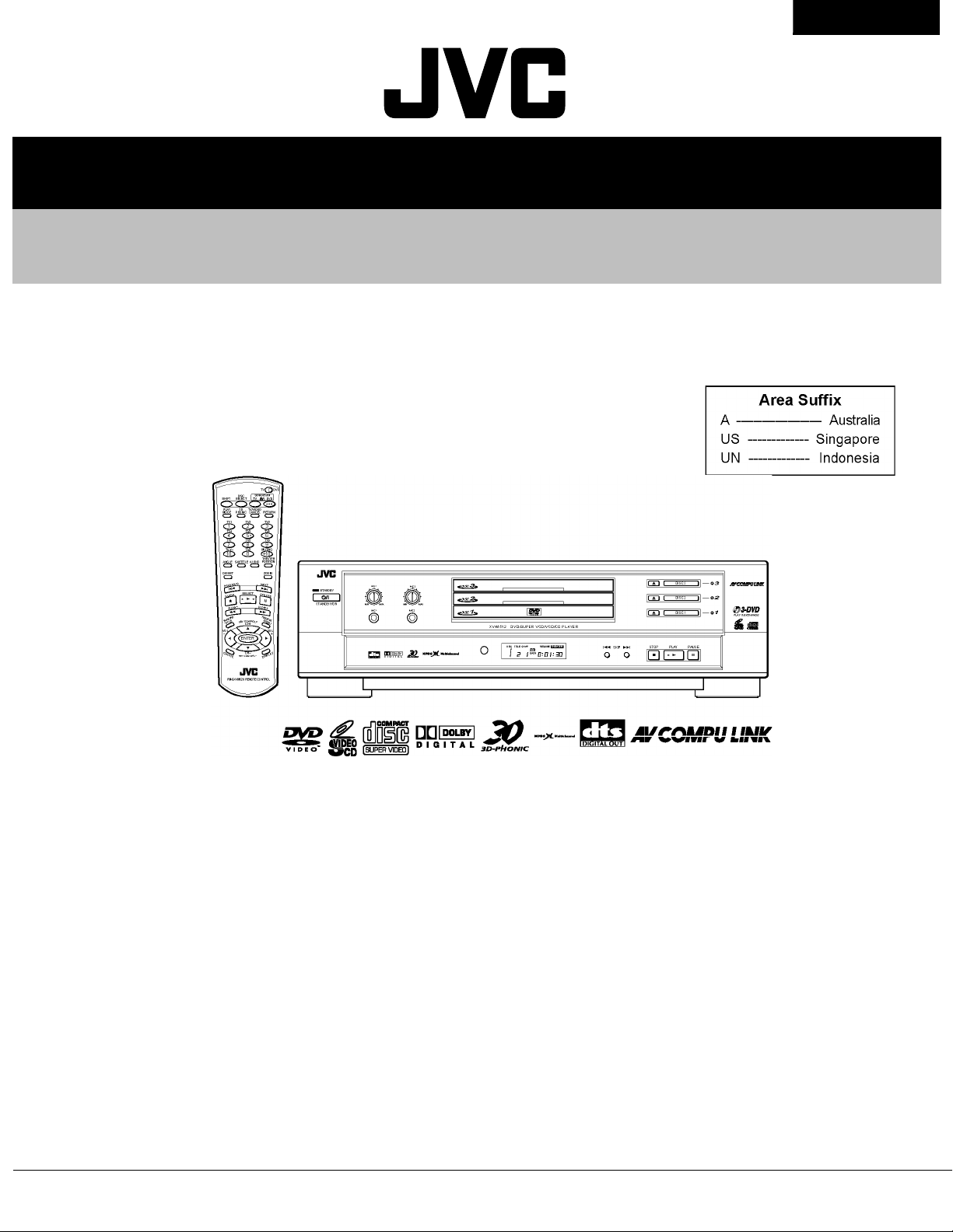
XV-M512SL
SERVICE MANUAL
DVD VIDEO PLAYER
XV-M512SL
TABLE OF CONTENTS
1 Important Safety Precautions . . . . . . . . . . . . . . . . . . . . . . . . . . . . . . . . . . . . . . . . . . . . . . . . . . . . . . . . . . . . . 2
2 Disassembly method . . . . . . . . . . . . . . . . . . . . . . . . . . . . . . . . . . . . . . . . . . . . . . . . . . . . . . . . . . . . . . . . . . . . 6
3 Mechanism . . . . . . . . . . . . . . . . . . . . . . . . . . . . . . . . . . . . . . . . . . . . . . . . . . . . . . . . . . . . . . . . . . . . . . . . . . . 12
4 Adjustment method . . . . . . . . . . . . . . . . . . . . . . . . . . . . . . . . . . . . . . . . . . . . . . . . . . . . . . . . . . . . . . . . . . . . 21
5 Description of major ICs . . . . . . . . . . . . . . . . . . . . . . . . . . . . . . . . . . . . . . . . . . . . . . . . . . . . . . . . . . . . . . . . 25
COPYRIGHT © 2002 VICTOR COMPANY OF JAPAN, LTD.
No.A0037
2002/11
Page 2
XV-M512SL
Important Safety Precautions
1.1 Safety Precautions
(1) This design of this product contains special hardware and
many circuits and components specially for safety purposes.
For continued protection, no changes should be made to the
original design unless authorized in writing by the
manufacturer. Replacement parts must be identical to
those used in the original circuits. Services should be
performed by qualified personnel only.
(2) Alterations of the design or circuitry of the product should
not be made. Any design alterations of the product should
not be made. Any design alterations or additions will void
the manufacturers warranty and will further relieve the
manufacture of responsibility for personal injury or property
damage resulting therefrom.
(3) Many electrical and mechanical parts in the products have
special safety-related characteristics. These characteristics are often not evident from visual inspection nor can the
protection afforded by them necessarily be obtained by
using replacement components rated for higher voltage,
wattage, etc. Replacement parts which have these special
safety characteristics are identified in the Parts List of Service
Manual. Electrical components having such features are
identified by shading on the schematics and by ( )
on the Parts List in the Service Manual. The use of a substitute replacement which does not have the same safety
characteristics as the recommended replacement parts
shown in the Parts List of Service Manual may create
shock, fire, or other hazards.
(4) The leads in the products are routed and dressed with ties,
clamps, tubings, barriers and the like to be separated from
live parts, high temperature parts, moving parts and/or
sharp edges for the prevention of electric shock and fire
hazard. When service is required, the original lead routing
and dress should be observed, and it should be confirmed
that they have been returned to normal, after reassembling.
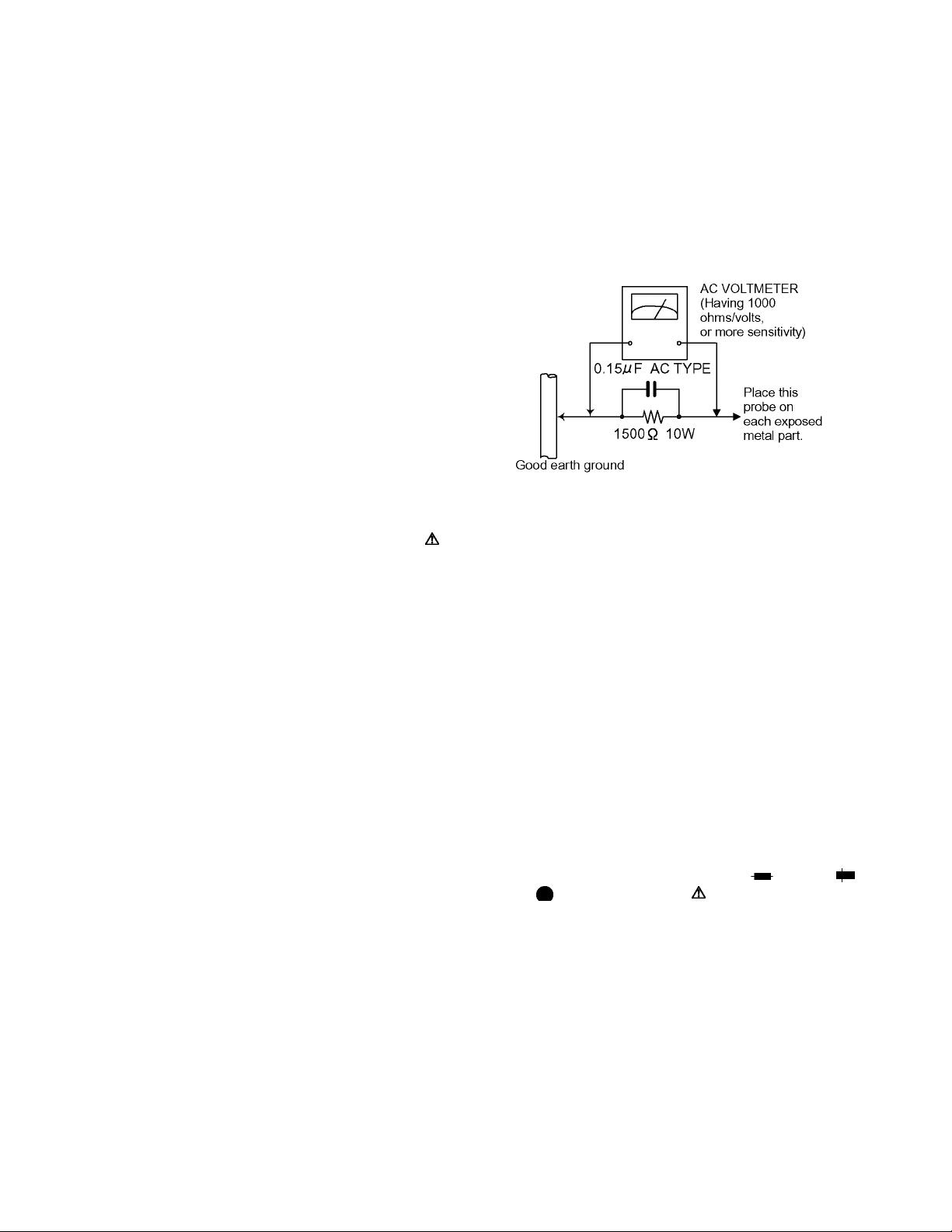
(5) Leakage shock hazard testing)
After reassembling the product, always perform an isolation
check on the exposed metal parts of the product (antenna
terminals, knobs, metal cabinet, screw heads, headphone
jack, control shafts, etc.) to be sure the product is safe to
operate without danger of electrical shock.
Do not use a line isolation transformer during this check.
• Plug the AC line cord directly into the AC outlet. Using a
"Leakage Current Tester", measure the leakage current
from each exposed metal parts of the cabinet, particularly any exposed metal part having a return path to the
chassis, to a known good earth ground. Any leakage
current must not exceed 0.5mA AC (r.m.s.).
• Alternate check method
Plug the AC line cord directly into the AC outlet. Use an AC
voltmeter having, 1,000 ohms per volt or more sensitivity in
the following manner. Connect a 1,500 ohm 10W resistor
paralleled by a 0.15 µF AC-type capacitor between an
exposed metal part and a known good earth ground.
Measure the AC voltage across the resistor with the AC
SECTION 1
voltmeter.
Move the resistor connection to each exposed metal part,
particularly any exposed metal part having a return path to
the chassis, and measure the AC voltage across the
resistor. Now, reverse the plug in the AC outlet and repeat
each measurement. Voltage measured any must not
exceed 0.75 V AC (r.m.s.). This corresponds to 0.5 mA AC
(r.m.s.).
1.2 Warning
(1) This equipment has been designed and manufactured to
meet international safety standards.
(2) It is the legal responsibility of the repairer to ensure that
these safety standards are maintained.
(3) Repairs must be made in accordance with the relevant
safety standards.
(4) It is essential that safety critical components are replaced
by approved parts.
(5) If mains voltage selector is provided, check setting for lo-
cal voltage.
1.3 Caution
Burrs formed during molding may be left over on some
parts of the chassis.
Therefore, pay attention to such burrs in the case of preforming repair of this system.
1.4 Critical parts for safety
In regard with component parts appearing on the silk-screen
printed side (parts side) of the PWB diagrams, the parts that are
printed over with black such as the resistor ( ), diode ( )
and ICP ( ) or identified by the " " mark nearby are critical
for safety.
When replacing them, be sure to use the parts of the same type
and rating as specified by the manufacturer. (Except the JC version)
2
Page 3
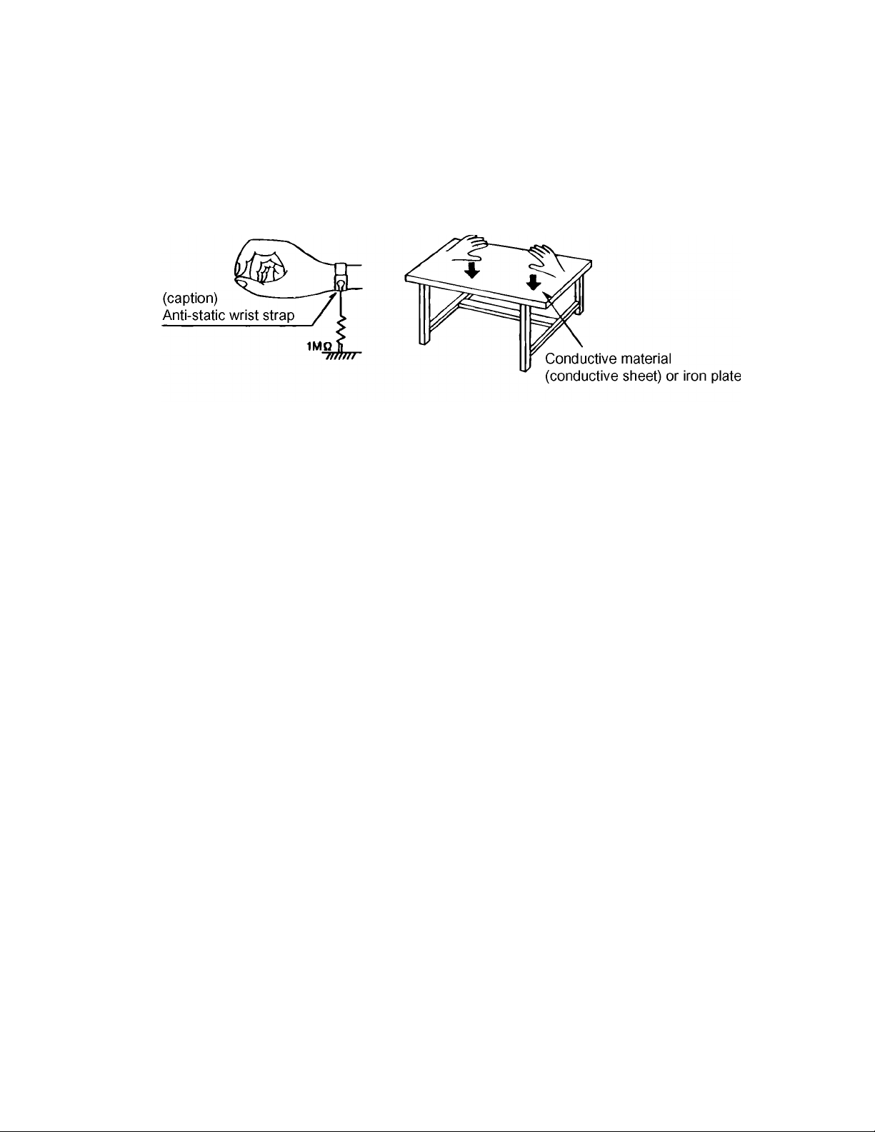
1.5 Preventing static electricity
Electrostatic discharge (ESD), which occurs when static electricity stored in the body, fabric, etc. is discharged,
can destroy the laser diode in the traverse unit (optical pickup). Take care to prevent this when performing repairs.
1.5.1 Grounding to prevent damage by static electricity
Static electricity in the work area can destroy the optical pickup (laser diode) in devices such as DVD players.
Be careful to use proper grounding in the area where repairs are being performed.
(1) Ground the workbench
Ground the workbench by laying conductive material (such as a conductive sheet) or an iron plate over it before placing the
traverse unit (optical pickup) on it.
(2) Ground yourself
Use an anti-static wrist strap to release any static electricity built up in your body.
(3) Handling the optical pickup
• In order to maintain quality during transport and before installation, both sides of the laser diode on the replacement optical
pickup are shorted. After replacement, return the shorted parts to their original condition.
(Refer to the text.)
• Do not use a tester to check the condition of the laser diode in the optical pickup. The tester's internal power source can
easily destroy the laser diode.
1.6 Handling the traverse unit (optical pickup)
XV-M512SL
(1) Do not subject the traverse unit (optical pickup) to strong shocks, as it is a sensitive, complex unit.
(2) Cut off the shorted part of the flexible cable using nippers, etc. after replacing the optical pickup. For specific details, refer to the
replacement procedure in the text. Remove the anti-static pin when replacing the traverse unit. Be careful not to take too
long a time when attaching it to the connector.
(3) Handle the flexible cable carefully as it may break when subjected to strong force.
(4)I t is not possible to adjust the semi-fixed resistor that adjusts the laser power. Do not turn it.
3
Page 4
XV-M512SL
1.7 Precautions for Service
1.7.1 Handling of Traverse Unit and Laser Pickup
(1) Do not touch any peripheral element of the pickup or the actuator.
(2) The traverse unit and the pickup are precision devices and therefore must not be subjected to strong shock.
(3) Do not use a tester to examine the laser diode. (The diode can easily be destroyed by the internal power supply of the tester.)
(4) When replacing the pickup, after mounting a new pickup, remove the solder on the short land which is provided at the center
of the flexible wire to open the circuit.
(5) Half-fixed resistors for laser power adjustment are adjusted in pairs at shipment to match the characteristics of the optical block.
Do not change the setting of these half-fixed resistors for laser power adjustment.
1.7.2 Destruction of Traverse Unit and Laser Pickup by Static Electricity
Laser diodes are easily destroyed by static electricity charged on clothing
or the human body. Before repairing peripheral elements of the traverse unit or pickup, be sure to take the following electrostatic
protection:
(1) Wear an antistatic wrist wrap.
(2) With a conductive sheet or a steel plate on the workbench on which the traverse unit or the pick up is to be repaired, ground
the sheet or the plate.
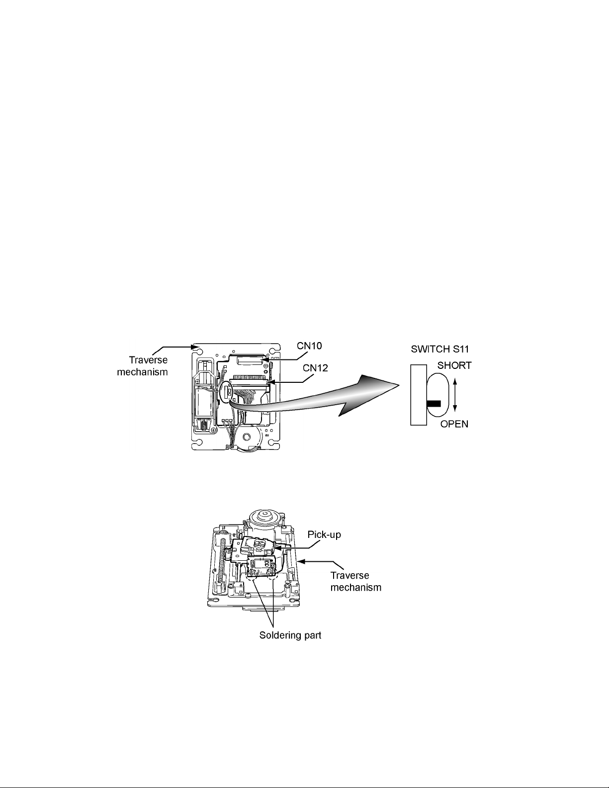
When you remove the traverse mechanism from the servo control substrate
The laser diode of pick-up might be destroyed by static electricity and set switch (S11) on the pick-up board on "SHORT" side, please
before removing the card wire from connector (CN10).
Moreover, please set switch (S11) on "OPEN" side after assembling and inserting the card wire in connector (CN10) without fail at
times.
When you remove the pick-up from the traverse mechanism
The laser diode of the pick-up might be destroyed by static electricity, and solder with part a, please before extracting a flexible wire
from connector (CN12).
Moreover, please remove solder in part a after inserting a flexible wire in connector (CN12).
4
Page 5

1.8 Important for laser products
(1) CLASS 1 LASER PRODUCT
(2) DANGER : Invisible laser radiation when open and inter
lock failed or defeated. Avoid direct exposure to beam.
(3) CAUTION : There are no serviceable parts inside the
Laser Unit. Do not disassemble the Laser Unit. Replace
the complete Laser Unit if it malfunctions.
(4) CAUTION : The compact disc player uses invisible laser
radiation and is equipped with safety switches which
prevent emission of radiation when the drawer is open and
the safety interlocks have failed or are de feated.
It is dangerous to defeat the safety switches.
VARNING
Osynlig laserstrålning är denna del är öppnad och spårren är
urkopplad. Betrakta ej strålen.
VARO
Avattaessa ja suojalukitus ohitettaessa olet alttiina näkymättömälle lasersäteilylle. Älä katso säteeseen.
XV-M512SL
(5) CAUTION : If safety switches malfunction, the laser is able
to function.
(6) CAUTION : Use of controls, adjustments or performance
of procedures other than those specified herein may result
in hazardous radiation exposure.
CAUTION
Please use enough caution not to see the beam directly
or touch it in case of anadjustment or operation check.
ADVARSEL
Usynlig laserstråling ved åbning, når sikkerhedsafbrydere er
ude af funktion. Undgå udsasttelse for stråling.
ADVARSEL
Usynlig laserstråling ved åpning, når sikkerhetsbryteren er
avslott. unngå utsettelse for stråling.
5
Page 6
XV-M512SL
SECTION 2
Disassembly method
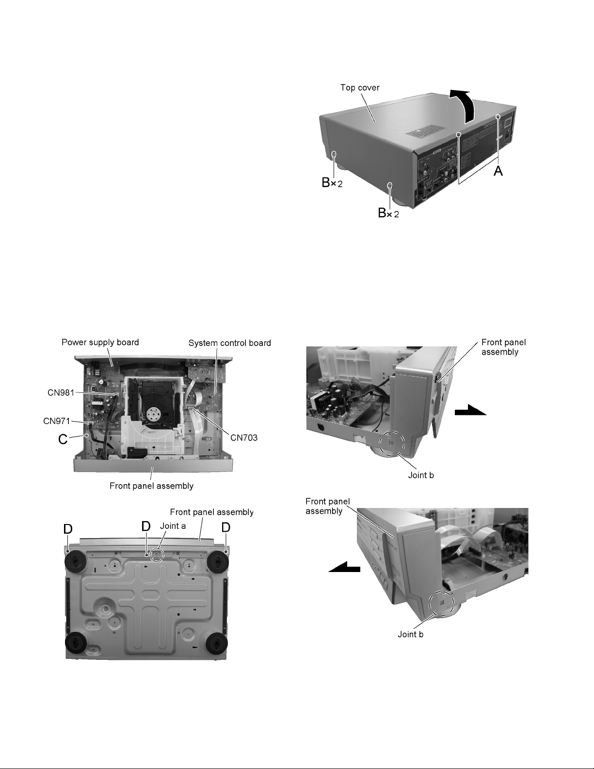
2.1 Main body
2.1.1 Removing the top cover
(See Fig.1)
(1) Remove the two screws A attaching the top cover on the
back of the body.
(2) Remove the four screws B attaching the top cover on both
sides of the body.
(3) Pull the lower parts of the top cover sides and remove the
top cover in the direction of the arrow.
Fig.1
2.1.2 Removing the front panel assembly
(See Fig.2 to 5)
• Prior to performing the following procedure, remove the top cover.
(1) Disconnect the wire from connector CN971 and CN981 on the power supply board.
(2) Remove the screw C attaching the lug wire on the chassis base.
(3) Disconnect the card wire from connector CN703 on the system control board.
(4) Remove the three screws D attaching the front panel assembly on the bottom of the body.
(5) Release the joint a on the bottom and the two joints b on both sides of the body. Remove the front panel assembly toward the
front.
Fig.4
Fig.2
Fig.5
Fig.3
6
Page 7
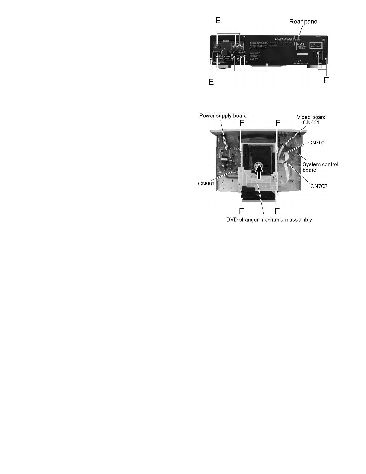
2.1.3 Removing the rear panel
(See Fig.6)
• Prior to performing the following procedure, remove the top
cover.
(1) Remove the eleven screws E attaching the rear panel on
the back of the body and detach the rear panel.
2.1.4 Removing the DVD changer mechanism assembly
(See Fig.7)
• Prior to performing the following procedure, remove the top
cover and front panel assembly.
(1) Disconnect the connector wire from connector CN961 on
the power supply board.
(2) Disconnect the card wire from connector CN601 on the
video board.
(3) Disconnect the card wires from connector CN701 and
CN702 on the system control board.
(4) Remove the four screws F attaching the DVD changer
mechanism assembly.
• It is easy for removing the front panel assembly to remove the
mechanism assembly though the mechanism assembly can
be removed even in the state that the front panel assembly
adheres.
XV-M512SL
Fig.6
Fig.7
7
Page 8
XV-M512SL
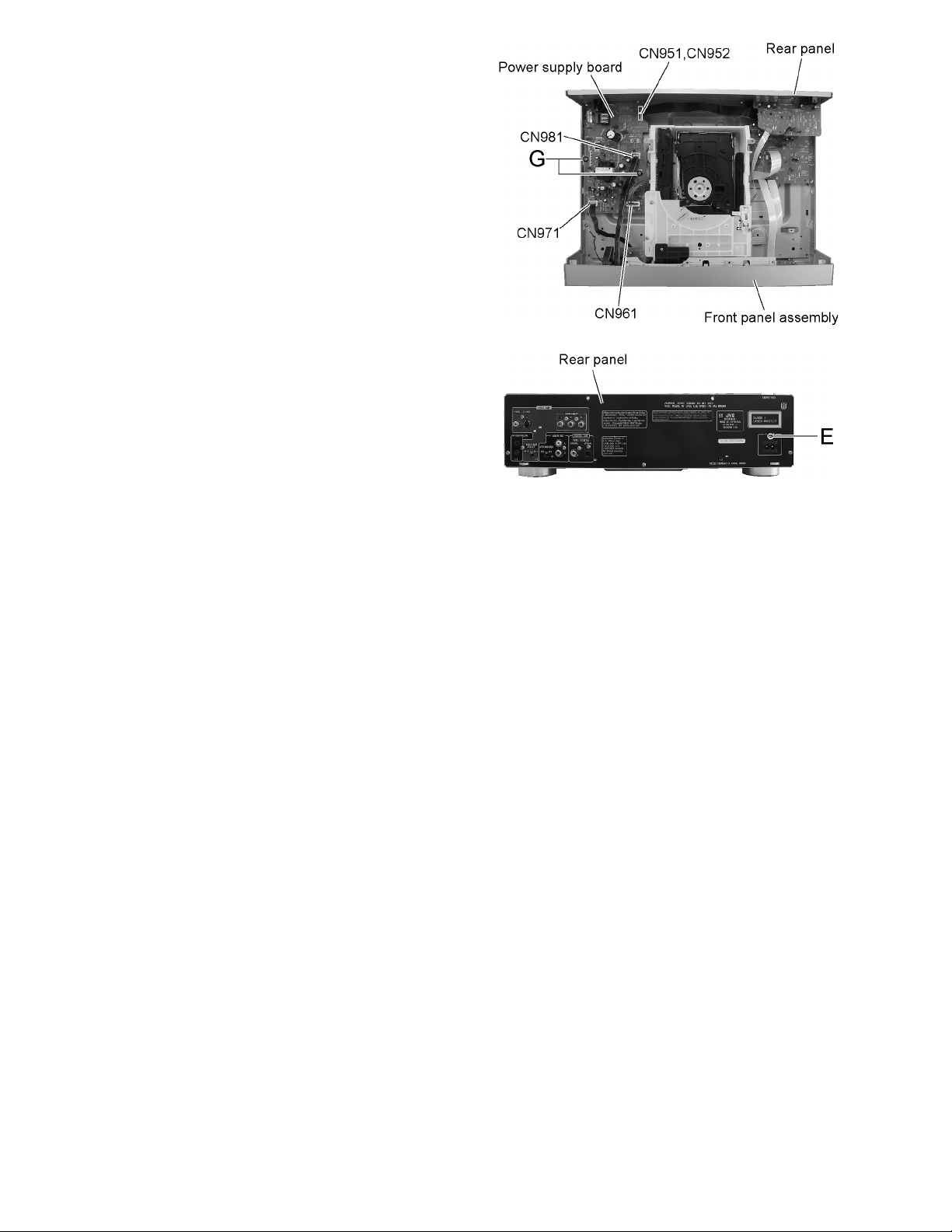
2.1.5 Removing the power supply board
(See Fig.8 and 9)
• Prior to performing the following procedure, remove the top
cover.
(1) Disconnect the wire from connector CN971 and CN981 on
the power supply board (The wire is extending from the
front panel assembly).
(2) Disconnect the connector wire from connector CN961 on
the power supply board (The wire is extending from the
DVD changer mechanism assembly).
(3) Disconnect the wire from connector CN951 and CN952 on
the power supply board (The wire is extending from the
system control board).
(4) Remove the screw E attaching the AC jack on the rear
panel.
(5) Remove the two screws G attaching the power supply
board and detach the power supply board.
Fig.8
Fig.9
8
Page 9
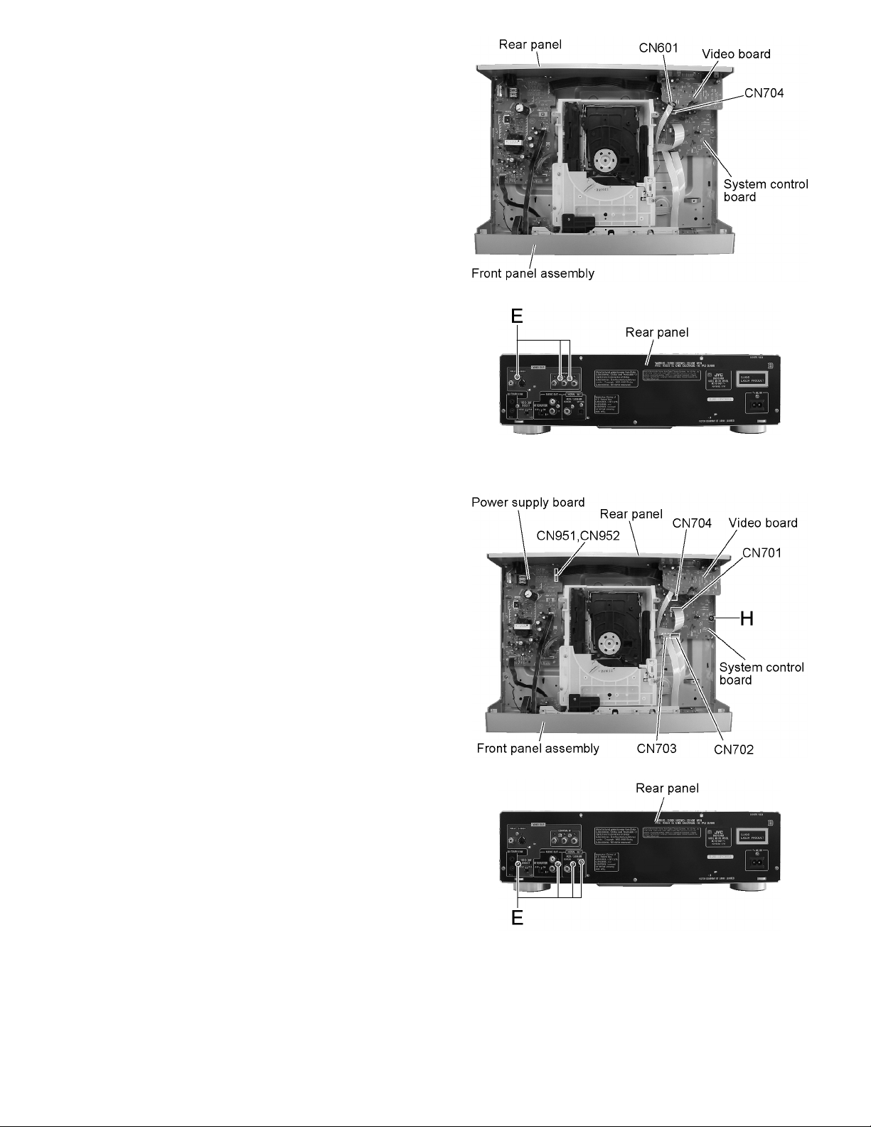
2.1.6 Removing the video board
(See Fig.10 and 11)
• Prior to performing the following procedure, remove the top
cover.
(1) Disconnect the card wire from connector CN601 on the
video board (The card wire is extending from the DVD
changer mechanism assembly).
(2) Disconnect the wire from connector CN704 on the system
control board (The wire is extending from the video board).
(3) Remove the three screws E attaching the video board on
the rear panel. Pull out the video board from the rear panel.
XV-M512SL
Fig.10
2.1.7 Removing the system control board
(See Fig.12 and 13)
• Prior to performing the following procedure, remove the top
cover.
• The system control board can be removed even if the video
board is attached.
(1) Disconnect the card wire from connector CN703 on the
system control board (The card wire is extending from the
front panel assembly).
(2) Disconnect the card wire from connector CN701 and
CN702 on the audio board (The card wires are extending
from the DVD changer mechanism assembly).
(3) Disconnect the wire from connector CN704 on the system
control board (The wire is extending from the video board).
(4) Disconnect the wire from connector CN951 and CN952 on
the power supply board (The wire is extending from the
system control board).
(5) Remove the screw H attaching the system control board.
(6) Remove the four screws E attaching the system control
board on the rear panel. Pull out the system control board
toward the front.
Fig.11
Fig.12
Fig.13
9
Page 10
XV-M512SL
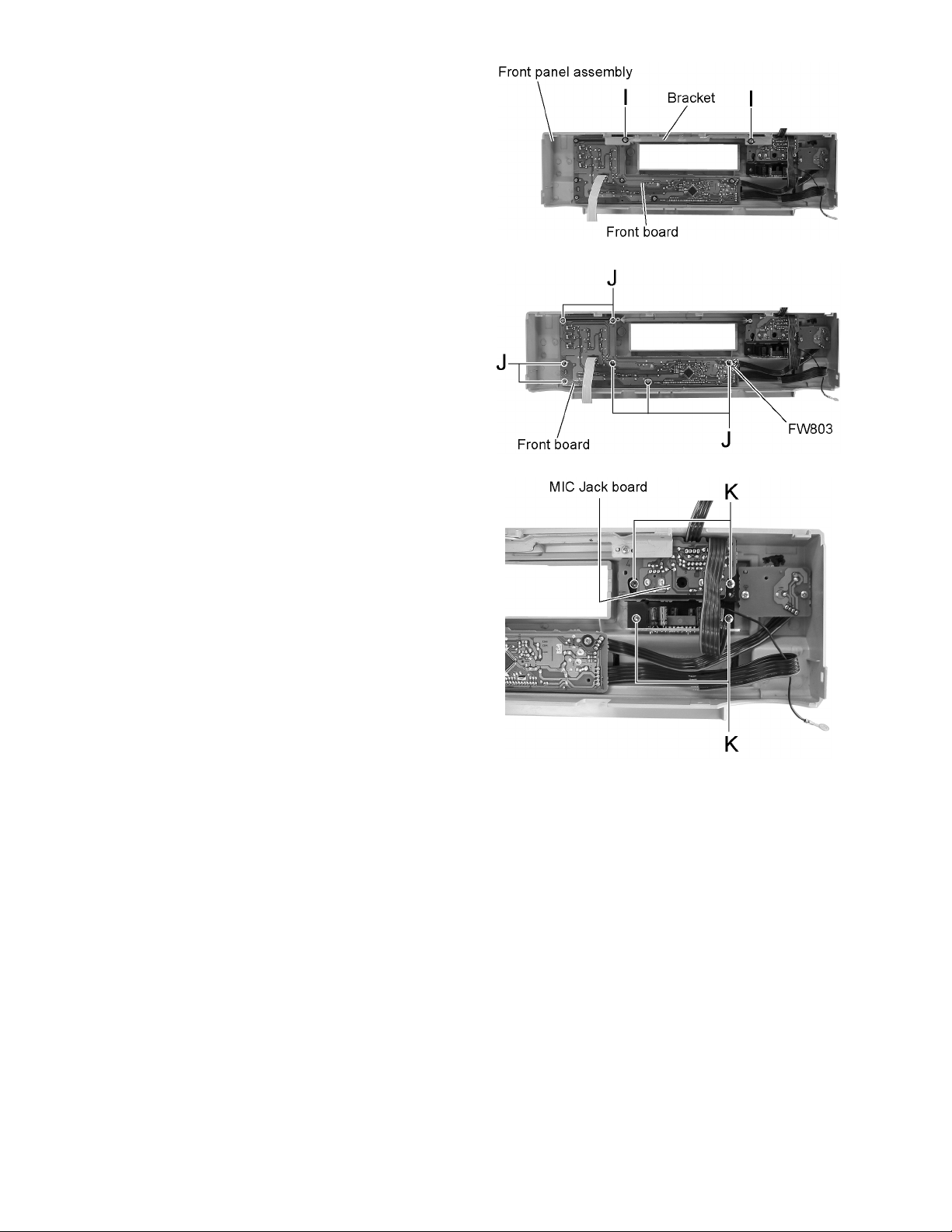
2.2 Front panel assembly
• Prior to performing the following procedure, remove the top
cover and the front panel assembly.
2.2.1 Removing the front board
(See Fig.14 and 15)
(1) Remove the two screws I on the back of the front panel
assembly and remove the bracket from the front panel assembly.
(2) Remove the seven screws J attaching the front board.
If necessary, unsolder FW803 and disconnect the wire.
2.2.2 Removing the MIC jack board
(See Fig.14 and 16)
(1) Remove the two screws I on the back of the front panel
assembly and remove the bracket from the front panel assembly.
(2) Remove the four screws K on the back of the front panel
assembly.
Fig.14
Fig.15
10
Fig.16
Page 11
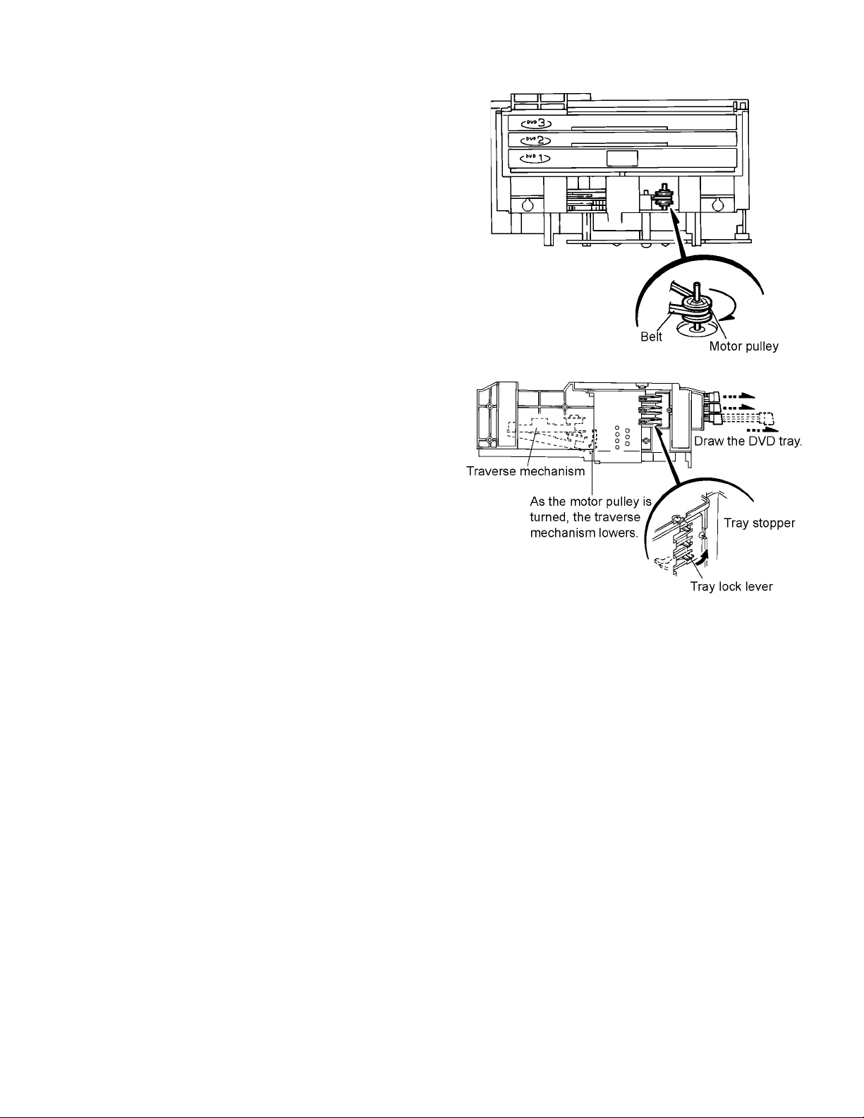
2.3 Ejecting the DVD
(See Fig.17 and 18)
2.3.1 When the DVD is set or the traverse mechanism is up.
note:
The DVD tray can not be ejected when the traverse mechanism is up.
2.3.2 Bringing down the traverse mechanism as shown in
the Fig.17 and 18
(1) The motor pulley and the belt can be seen on the front side
of the changer. Turn the motor pulley clockwise until the
belt stops.
(2) Pull the tray lock lever on the left side of the changer and
draw the DVD tray.
(3) Draw the DVD tray 1 to 3 as above.
XV-M512SL
Fig.17
Fig.18
11
Page 12
XV-M512SL
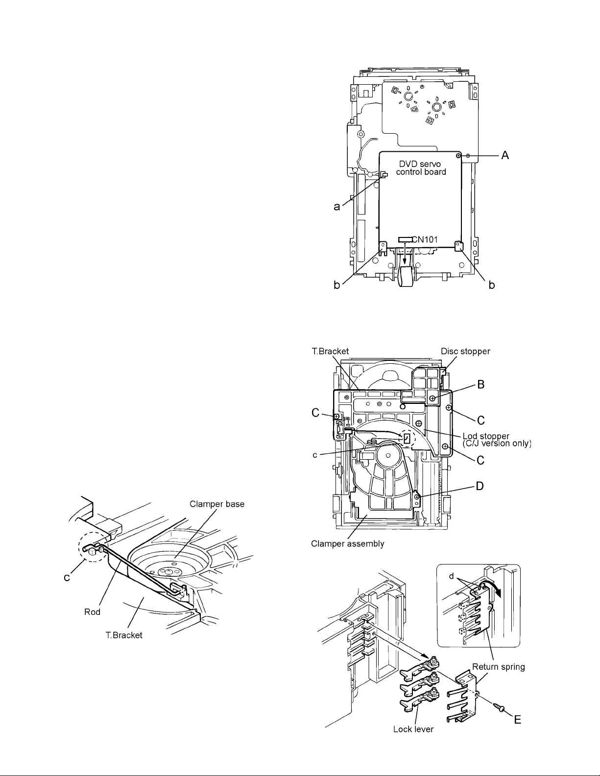
3.1 DVD Changer Mechanism Section
3.1.1 Removing the DVD mechanism board
(See Fig.1)
(1) Remove the DVD changer mechanism assembly.
(2) From bottom side the DVD changer mechanism assem-
bly, remove the one screw A retaining the DVD servo control board.
(3) Disconnect the card wire from the connector CN101 on the
DVD servo control board.
(4) Disengage the one engagement a and two engagements
b, remove the DVD servo control board.
ATTENTION:
The laser diode of pick-up might be destroyed by static electricity and set switch (S11) on the pick-up board on “SHORT”
side, please before removing the card wire from connector
(CN101).
Moreover, please set switch (S11) on “OPEN” side after assembling and inserting the card wire in connector (CN101)
without fail at times.
SECTION 3
Mechanism
3.1.2 Removing the DVD tray assembly
(See Fig.2 to 4)
(1) Remove the screw B retaining the Disc stopper (See
Fig.3).
(2) Remove the three screws C retaining the T.bracket (See
Fig.3).
(3) From the clamper base section c, remove both of the edg-
es fixing the rod (See Fig.2 and 3).
(4) Remove the screw D retaining the clamper assembly
(See Fig.3).
(5) From the left side face of the chassis assembly, remove
the one screw E retaining both of the return spring and
lock lever (See Fig. 4).
(6) By removing the pawl at the section d fixing the return
spring, dismount the return spring (See Fig.4).
(7) Remove the three lock levers (See Fig.4).
Fig.1
Fig.3
12
Fig.2
Fig.4
Page 13
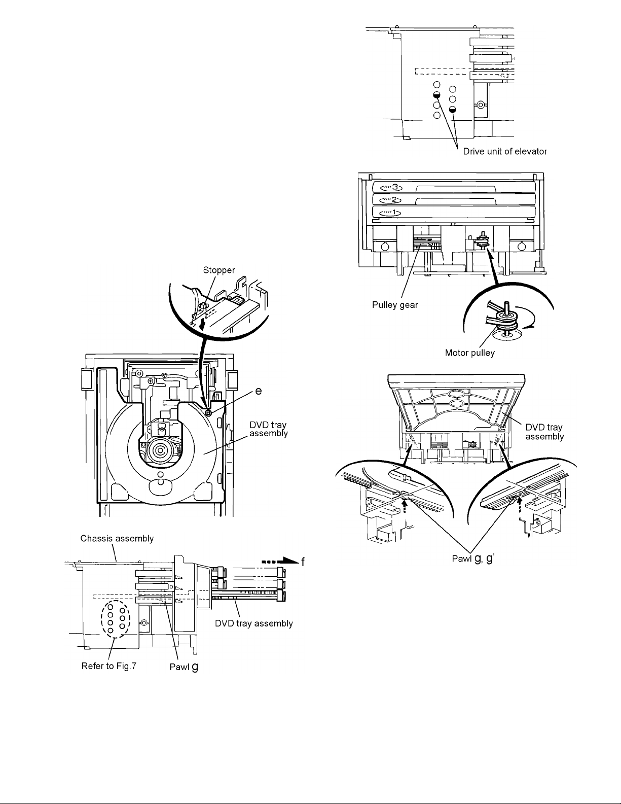
(8) Check whether the lifter unit stopper has been caught into
the hole at the section e of DVD tray assembly as shown
in Fig.5.
(9) Make sure that the driver unit elevator is positioned as
shown in Fig.6 from to the second or fifth hole on the left
side face of the DVD Traverse mechanism assembly.
Caution:
In case the driver unit elevator is not at above position,
set the elevator to the position as shown in Fig.7 by
manually turning the pulley gear as shown in Fig.8.
(10) Manually turn the motor pulley in the clockwise direction
until the lifter unit stopper is lowered from the section e of
DVD tray assembly (See Fig.8).
(11) Pull out all of the three stages of DVD tray assembly in the
arrow direction f until these stages stop (See Fig.6).
(12) At the position where the DVD tray assembly has stopped,
pull out the DVD tray assembly while pressing the two
pawls g and g' on the back side of DVD tray assembly
(See Fig.9). In this case, it is easy to pull out the assembly
when it is pulled out first from the stage DVD tray assembly.
XV-M512SL
Fig.7
Fig.5
Fig.8
Fig.9
Fig.6
13
Page 14
XV-M512SL
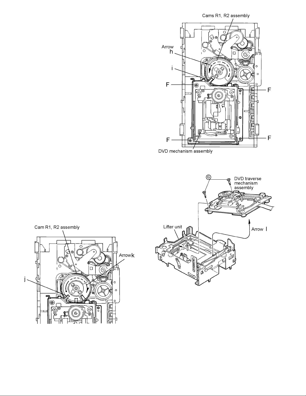
3.1.3 Removing the DVD mechanism assembly
(See Fig.10)
(1) While turning the cams R1 and R2 assembly in the arrow
direction h, align the shaft i of the DVD mechanism assembly to the position shown in Fig.10.
(2) Remove the four screw F retaining the DVD mechanism
assembly.
3.1.4 Removing the DVD traverse mechanism assembly
(See Fig.11 and 12)
(1) For dismounting only the DVD mechanism without remov-
ing the DVD mechanism assembly, align the shaft j of the
DVD mechanism assembly to the position shown Fig.11
while turning the cam R1 and R2 assembly in the arrow direction k.
(2) Remove the two screws G raising the DVD mechanism
assembly.
(3) Remove the DVD traverse mechanism assembly in the ar-
row direction I from the lifter unit (See Fig.12)
Fig.10
Fig.12
14
Fig.11
Page 15
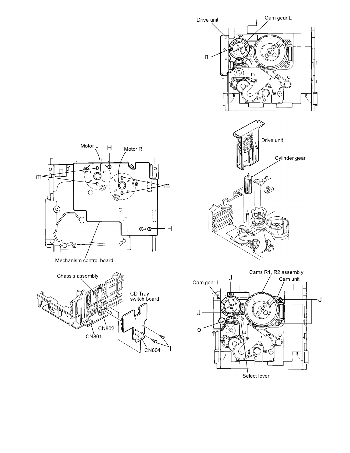
3.1.5 Removing the mechanism control board
(See Fig.14, 15)
(1) Absorb the four soldered positions m of the right and left
motors with a soldering absorber (See Fig.14).
(2) Remove the two screws H retaining the mechanism con-
trol board (See Fig.14).
(3) Remove the two screws I retaining the tray select switch
board (See Fig.15).
3.1.6 Removing the cam unit
(See Fig.15 to 18)
(1) Remove the DVD mechanism assembly.
(2) While turning the cam gear L, align the pawl n position of
the drive unit to the notch position (Fig.15) on the cam
gear L.
(3) Pull out the drive unit and cylinder gear (See Fig.17).
(4) While turning the cam gear L, align the pawl o position of
the select lever to the notch position (Fig.18) on the cam
gear L.
(5) Remove the four screws J retaining the cam unit (cam
gear L and cams R1/R2 assembly)(See Fig.18).
XV-M512SL
Fig.16
Fig.14
Fig.15
Fig.17
Fig.18
15
Page 16
XV-M512SL
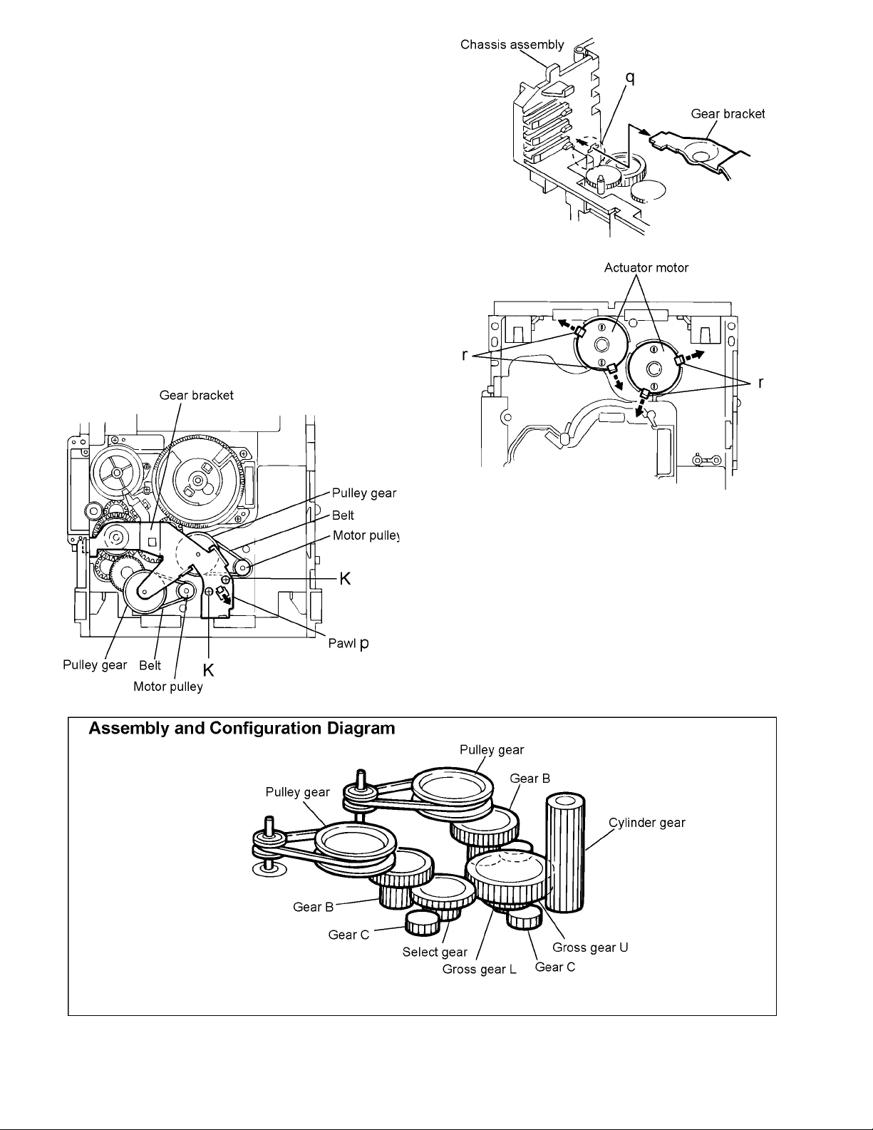
3.1.7 Removing the actuator motor and belt
(See Fig.19 to 22)
(1) Remove the two screws K retaining the gear bracket (See
Fig.19).
(2) While pressing the pawl p fixing the gear bracket in the ar-
row direction, remove the gear bracket (See Fig.19).
(3) From the notch q section on the chassis assembly fixing
the edge of gear bracket, remove and take out the gear
bracket (See Fig.20).
(4) Remove the belts respectively from the right and left actu-
ator motor pulleys and pulley gears (See Fig.19).
(5) After turning over the chassis assembly, remove the actu-
ator motor while spreading the four pawls r fixing the right
and left actuator motors in the arrow direction (See Fig.
21).
Note:
When the chassis assembly is turned over under the conditions wherein the gear bracket and belt have been removed,
then the pulley gear as well as the gear, etc. constituting the
gear unit can possibly be separated to pieces. In such a case,
assemble these parts by referring to the assembly and configuration diagram in Fig.22.
Fig.20
Fig.19
Fig.21
16
Fig.22
Page 17
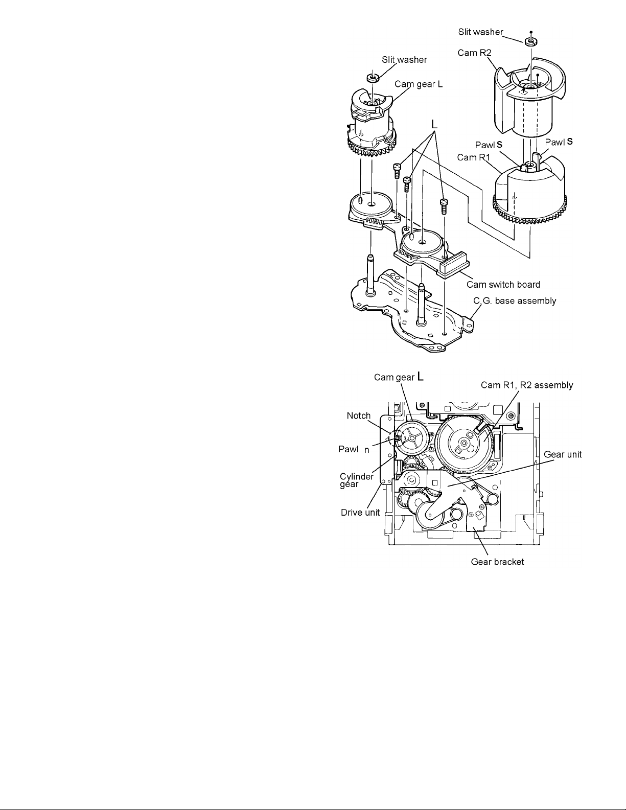
3.1.8 Removing the cams R1/R2 assembly and cam gear L
(See Fig.23)
(1) Remove the slit washer fixing the cams R1 and R2 assem-
bly.
(2) By removing the two pawls s fixing the cam R1, separate
R2 from R1.
(3) Remove the slit washer fixing the cam gear L.
(4) Pull out the cam gear L from the C.G. base assembly.
3.1.9 Removing the C.G. base assembly
(See Fig.23 and 24)
Remove the three screws L retaining the C.G. base assembly.
Caution:
To reassemble the cylinder gear, etc.with the cam unit (cam
gear and cams R1/R2 assembly), gear unit and drive unit,
align the position of the pawl n on the drive unit to that of the
notch on the cam gear L. Then, make sure that the gear unit
is engaged by turning the cam gear L (See Fig. 24).
XV-M512SL
Fig.23
Fig.24
17
Page 18

XV-M512SL
3.2 DVD Traverse mechanism section
3.2.1 Removing the pickup
(See Fig.25 to 29)
(1) Solder soldering a on the flexible board next to the pickup
unit.
(2) From the bottom of the traverse mechanism unit, discon-
nect the flexible wire from CN12 on the pickup board.
ATTENTION:
The laser diode of the pick-up might be destroyed by
static electricity, and solder with part a, please before
extracting a flexible wire from connector (CN12).
Moreover, please remove solder in part a after inserting
a flexible wire in connector (CN12).
(3) Remove the screw A attaching the shaft stopper (R) on
the upper side of the traverse mechanism unit. Pull the
side of the shaft stopper (R) outward to release the joint b
and remove it upward. Remove the skew spring at the
same time.
(4) Move the shaft in the direction of the arrow to release it
from the part c.
(5) Release the joint d with the shaft and remove the pickup
with the shaft.
(6) Pull out the shaft.
(7) Remove the screw B attaching the switch actuator.
Fig.27
Fig.25
Fig.26
Fig.28
Fig.29
18
Page 19

3.2.2 Removing the pickup board
(See Fig.25 and 30)
(1) Solder soldering a on the flexible board next to the pickup
unit.
(2) From the bottom of the traverse mechanism unit, discon-
nect the flexible wire from CN12 on the pickup board.
ATTENTION:
The laser diode of the pick-up might be destroyed by
static electricity, and solder with part a, please before
extracting a flexible wire from connector (CN12).
Moreover, please remove solder in part a after inserting
a flexible wire in connector (CN12).
(3) Unsolder soldering e, f and g of each harness on the pick-
up board.
(4) Remove the screw C attaching the pickup board and re-
lease the two joints h.
3.2.3 Removing the feed motor assembly
(See Fig.25, 30 and 31)
(1) Solder soldering a on the flexible board next to the pickup
unit.
(2) From the bottom of the traverse mechanism unit, discon-
nect the flexible wire from CN12 on the pickup board.
ATTENTION:
The laser diode of the pick-up might be destroyed by
static electricity, and solder with part a, please before
extracting a flexible wire from connector (CN12).
Moreover, please remove solder in part a after inserting
a flexible wire in connector (CN12).
(3) Unsolder soldering e of the motor harness on the pickup
board.
(4) Remove the two screws D attaching the feed motor as-
sembly and remove the thrust spring. Move the feed motor
assembly in the direction of the arrow to pull it out from the
feed holder.
XV-M512SL
Fig.25
Fig.30
Fig.31
19
Page 20

XV-M512SL
3.2.4 Removing the turn table assembly
(See Fig.25, 30, 32 and 33)
(1) Solder soldering a on the flexible board next to the pickup
unit.
(2) From the bottom of the traverse mechanism unit, discon-
nect the flexible wire from CN12 on the pickup board.
ATTENTION:
The laser diode of the pick-up might be destroyed by
static electricity, and solder with part a, please before
extracting a flexible wire from connector (CN12).
Moreover, please remove solder in part a after inserting
a flexible wire in connector (CN12).
(3) Unsolder soldering f and g of the harness extending from
the turn table assembly to the pickup board.
(4) Remove the screw E attaching the shaft stopper (F) on
the upper side of the traverse mechanism unit. Pull the
side of the shaft stopper (F) outward to release the joint i
and remove it upward. Remove the spring at the same
time.
(5) Remove the screw F attaching the turn table assembly.
(6) Move the turn table assembly outward and pull out from
the shaft. Then remove it from the base chassis.
Fig.32
Fig.25
Fig.30
Fig.33
20
Page 21

XV-M512SL
SECTION 4
Adjustment method
4.1 Initialization method
If microprocessor (IC401,IC402,IC403) or pick-up is replaces, initialize the DVD player in the following matter
(1) Take out the disc and close the tray.
(2) Unplug the power plug.
(3) Insert power plug into outlet while pressing both PLAY button and DISC 1 OPEN/CLOSE button.
(4) FL Display indicate “tESt ¥” . :Version, ¥ :Region code
(5) Press 3D-PHONIC key button of remote controller. and EEPROM initialize start.
(6) When indicate “V.REPLACE” on the display, initialize finishes.
(7) The power is turned OFF, and Unplug the power plug.
4.2 Display of “Laser current value” and “Jitter value”
“Laser current value” and “Jitter value” are displayed on the FL display by the undermentioned method. Please refer to
the failure diagnosis.
(1) Take out the disc and close the tray.
(2) Unplug the power plug.
(3) Insert power plug into outlet while pressing both PLAY button and DISC 1 OPEN/CLOSE button.
(4) FL Display indicate “tESt ¥” . :Version, ¥ :Region code
(5) Press the “OPEN/CLOSE” button to move the tray outward.
Put the test disc (VT-501) on the tray and press “OPEN/CLOSE” button.
The tray should move inward (Note:Don't push to close the tray directly by hand etc.)
(6) Press the “PLAY” button.
(7) The laser current value and the jitter value is displayed on the FL indicator as follows.
4.2.1 For Laser current value
Becomes a test mode by doing above-mentioned procedure (1) - (4). Afterwards, the laser current value can be switched by pushing
the key to remote controller without turning on the disk.
Remote control “4” key --- Laser of CD
Remote control “5” key --- Laser of DVD
*Returns to a usual test mode by the thing to push the stop button of remote controller.
* As for the current value of the laser, the figure displayed on the LCD display becomes a current value as it is by “mA” unit. becomes
40 mA if displayed as 40.
* It can be judged it is simply good if the displayed current value of the laser is smaller than that of the undermentioned
value.
Moreover, there must be a deteriorated possibility and the pick-up must exchange the pick-up more than the undermentioned value.
Laser current value of CD ------ 49 mA or less
Laser current value of DVD ---- 64 mA or less
21
Page 22

XV-M512SL
4.2.2 For Jitter value
The jitter value is displayed by the hexadecimal number and refer to the conversion table of following,please.
If the indication value is 11% or less, it can be judged by this simple checking method that the signalread precision of the set is satisfactory.
Before using the TEST disc VT-501, careful check it if there is neither damage nor dirt on the read surface.
4.2.3 Jitter value
FL display
3818 4.7 3998 7.6
3828 4.8 39A8 7.7
3838 4.9 39B8 7.8
3848 5.1 39C8 7.9
3858 5.2 39D8 8.1
3868 5.3 39E8 8.2
3878 5.4 39F8 8.3
3888 5.5 3A18 8.5
3898 5.7 3A28 8.7
38A8 5.8 3A38 8.8
38b8 5.9 3A48 8.9
38c86.03A589.0
38d8 6.1 3A68 9.1
38E8 6.3 3A78 9.3
38F8 6.4 3A88 9.4
3918 6.6 3A98 9.5
3928 6.7 3AA8 9.6
3938 6.9 3AB8 9.7
3948 7.0 3AC8 9.9
3958 7.1 3AD8 10.0
3968 7.2 3AE8 10.1
3978 7.3 3AF8 10.2
3988 7.5
Conversion
value(%)
FL display
Conversion
value(%)
FL display
3B18 10.5 3C98 13.3
3B28 10.6 3CA8 13.5
3B38 10.7 3CB8 13.6
3B48 10.8 3CC8 13.7
3B58 10.9 3CD8 13.8
3B68 11.1 3CE8 13.9
3B78 11.2 3CF8 14.1
3B88 11.3 3D18 14.3
3B98 11.4 3D28 14.4
3BA8 11.5 3D38 14.5
3BB8 11.7 3D48 14.7
3BC8 11.8 3D58 14.8
3BD8 11.9 3D68 14.9
3BE8 12.0 3D78 15.0
3BF8 12.1 3D88 15.1
3C18 12.4 3D98 15.3
3C28 12.5 3DA8 15.4
3C38 12.7 3DB8 15.5
3C48 12.7 3DC8 15.6
3C58 12.9 3DD8 15.7
3C68 13.0 3DE8 15.9
3C78 13.1 3DF8 16.0
3C88 13.2
Conversion
value(%)
FL display
Conversion
value(%)
22
Page 23

4.3 Flap adjustment of the pick-up guide shaft
Note:
When replacing a pickup etc., execute the following adjustments
4.3.1 Pickup replacement
(1) When removing the traverse mechanism from the changer
mechanism unit, move the pickup to the innermost diameter of the disc and set switch (S11) on the pick-up board
on “SHORT” side, please before removing the card wire
from connector (CN10)
(2) Take out the traverse mechanism.
(3) First short-circuit the pickup circuit before removing the
pickup. Then carry out the replacement.
XV-M512SL
4.3.2 Jig setup
(1) Remove the rubber cushion from each of the four corners
of the traverse mechanism.
(When installing be sure not to make a mistake with the
cushion colors).
(2) Install the jig stud.
(3) Make a jig clamp. (Remove the clamp from the set and as-
semble it as shown in the diagram below.
Note:
How to handle the pickup
To protect the pickup from electro-static damage, make sure
to hold it by the die-cast chassis (optical base). And make
sure that pickup lens do not touch the top cover.
23
Page 24

XV-M512SL
4.3.3 Integrated wiring for adjustment
(1) Place a board on top of the unit and put the changer on it.
Then carry out the wiring of the main unit.
(2) Connect a extension cable to the traverse mechanism for
adjustment and then connect them to the changer.
(3) Remove the solder of the short-circuited flexible wire.
Then remove the short-circuited pin from the traverse
mechanism
(4) Connection is completed.
4.3.4 Adjustment preparation
(1) The 3 adjustment locations
(2) 1.4 mm hexagonal wrench
(3) Set the VT-501 or the VT502 test disc.
4.3.5 FL jitter display
(1) Connect the power cable while pressing the (OPEN/
CLOSE) button of DISC1 and (PLAY) button simultaneously.
--- The DISC no. “ ” is displayed on the FL indicator.
(2) Press the 3D-PHONIC key button of remote controller to
commence initialization.
(3) When the key (PLAY) is pressed the jitter value is dis-
played.
(4) Adjust the jitter value to minimum by using the adjust
screw.
a) Turn the adjustment screw (A and B) clockwise half.
b) Return the adjustment screw (A and B) to former po-
sition.
c) Turn the adjustment screw (A and B) counterclock-
wise half.
d) Set the adjustment screw (A and B) to the position of
best jitter at three positions.
Next, do it similar to the above-mentioned in adjustment screw
A and C.
24
Page 25

5.1 AK5353VT-X(IC511) : Converter
• Terminal layout
• Block diagram
XV-M512SL
SECTION 5
Description of major ICs
25
Page 26

XV-M512SL
• Pin function
No. Pin name I/O Function
1 AINR I Rch Analog input pin
2 AINL I Lch Analog input pin
3 VREF O Voltage Reference Output Pin
Normally connected to AGND with a 0.1µ F ceramic capacitor in parallel with an electrolytic
capacitor less than 4.7µ F.
4 VCOM O Common Voltage Output Pin
Normally connected to AGND with a 0.1µ F ceramic capacitor in parallel with an electrolytic
capacitor less than 4.7µ F.
5 AGND - Analog Ground Pin, 0V
6 VA - Analog Power Supply Pin, +2.7~+5.5V
7 VD - Digital Power Supply Pin, +2.7~+5.5V
8 DGND - Digital Ground Pin, 0V
9 SDTO O Serial Data Output Pin
Data bits are presented MSB first, in 2's complement format.
This pin is "L" in the power-down mode.
10 LRCK I Left/Right Channel Select pin
The fs clock is input to this pin.
11 MCLK I Master Clock Input Pin
12 SCLK I Serial Data Input Pin
Output data is clocked out on the falling edge of SCLK.
13 PDN I Power-Down Pin
When "L", the circuit is in power-down mode
The AK5353 should always be reset upon power-up.
14 DIF I Serial Interface Format Pin
L :MSB justified, "H": I
2
S
15 TTL I Digital Input Level Select Pin
L : CMOS level (VA,VD = 2.7~5.5V), "H" : TTL level (VA,VD=4.5~5.5V)
16 TST I Test Pin (Internal pull-down pin)
This pin should be left floating.
Note :
All input pins except pull-down pins should not be left floating.
26
Page 27

5.2 AK93C65AF-X (IC403) : EEPROM
• Pin layout
• Block diagram
XV-M512SL
• Pin function
Pin no. Symbol Function
1 PE Program enable (With built-in pull-up resistor)
2 VCC Power supply
3 CS Chip selection
4 SK Cereal clock input
5 DI Cereal data input
6 DO Cereal data output
7 GND Ground
8 NC No connection
NOTE :
The pull-up resistor of the PE pin is about 2.5Mohm (VCC=5V)
27
Page 28

XV-M512SL
5.3 AN8702FH(IC101):Frontend processor
• Pin layout
• Pin function
Pin No. Symbol I/O Description
1 PC1 I Input for Laser current monitor
2 PC01 O Laser power control output for DVD
3 PC2 I Photo detector fo CD
4 PC02 O Laser power control output for CD
5 TGBAL I Tangential phase balance control terminal
6 TBAL I Tracking balance control terminal
7 FBAL I Focus balance control ter
8 POFLT O Track detection threshold level terminal
9 DTRD I Data slice part data read signal input terminal (For RAM)
10 IDGT I Data slice part address part gate signal input terminal (For RAM)
11 STANDBY I Standby mode control terminal
12 SEN I SEN(Serial data input terminal)
13 SCK I SCK(Serial data input terminal)
14 STDI I STDI(Serial data input terminal)
15 RSEL I DVD and CD selection
16 JLINE I J-line setting output (FEP)
17 TEN I Tracking error output amplifier reversing input terminal
18 TEOUT O Tracking error signal output terminal
19 ASN I Off set adjustment terminal for DRC
20 ASOUT O All added signal output terminal
21 FEN I Focus error output amplifier reversing input terminal
22 FEOUT O Focus error signal output terminal
23 VSS - Connect to GND
24 TG O Tangential phase error signal output terminal
25 VDD - Power supply terminal 3V
26 GND2 - Connect to GND
27 VREF2 O VREF2 voltage output terminal
28 VCC2 - Power supply terminal 5V
29 VHALF O VHALF voltage output terminal
30 DFLTON O Filter amplifier reversing output terminal
31 DFLTOP O Filter amplifier output terminal
32 DSFLT O Connected capacitor terminal for filter output
33 GND3 - Connect to GND
34 RFDIFO O RF operation output terminal
35 RFOUT O RF output terminal
36 VCC3 - Power supply terminal 5V
37 RFC I Filter for RF amplifier
38 DCRF O All addition amplifier capacitor terminal
28
Page 29

Pin No. Symbol I/O Description
39 OFTR O OFTR output teminalr
40 BDO O BDO output terminal
41 RFENV O RF envelope output terminal
42 BTTOM O Bottom envelope detection filter terminal
43 PEAK O Peak envelope detection filter terminal
44 AGCG O AGC amplifier gain control teminalr
45 AGCO O AGC amplifier level control terminal
46 TESTSG I TEST signal input terminal
47 RFINP I RF signal positive input terminal
48 RFINN I RF signal negative input terminal
49 VIN5 I RF input of external division into 4 terminal for CD
50 VIN6 I RF input of external division into 4 terminal for CD
51 VIN7 I RF input of external division into 4 terminal for CD
52 VIN8 I RF input of external division into 4 terminal for CD
53 VIN9 I RF input of external division into 2 terminal for DVD
54 VIN10 I RF input of external division into 2 terminal for DVD
55 VCC1 - Power supply terminal 5V
56 VREF1 O VREF1 voltage output terminal
57 VIN1 I External division into four (DVD/CD) RF input terminal1
58 VIN2 I External division into four (DVD/CD) RF input terminal2
59 VIN3 I External division into four (DVD/CD) RF input terminal3
60 VIN4 I External division into four (DVD/CD) RF input terminal4
61 GND1 - Connect to GND
62 VIN11 I 3 beem sub input terminal for CD
63 VIN12 I 3 beem sub input terminal for CD
64 HDTYPE I HD type switching
XV-M512SL
29
Page 30

XV-M512SL
5.4 HY57V161610DTC8(IC504,IC505) : 16MB SDRAM
• Block diagram
• Pin function
Pin No. Symbol Description
1 VCC Power supply
2,3 DQ0,1 Data input/output
4 VSS Connect to GND
5,6 DQ2,3 Data input/output
7 VDD Power supply
8,9 DQ4,5 Data input/output
10 VSS Connect to GND
11,12 DQ6,7 Data input/output
13 VCC Power supply
14 LDQM Lower DQ mask enable
15
16
17
18
19,20 A11,10 Address inputs
21~24 A0~3 Address inputs
25 VCC Power supply
26 VSS Connect to GND
27~32 A4~9 Address inputs
33 NC Non connect
34 CKE Clock enable
35 CLK System clock input
36 UDQM Upper DQ mask enable
37 NC Non connect
38 VCC Power supply
39,40 DQ8,9 Data input/output
41 VSS Connect to GND
42,43 DQ10,11 Data input/output
44 VDD Power supply
45,46 DQ12,13 Data input/output
47 VSS Connect to GND
48,49 DQ14,15 Data input/output
50 VSS Connect to GND
WE
CAS
RAS
CS
Write enable
Column address strobe
Row address strobe
Chip enable
30
Page 31

5.5 M35500AFP(IC802) : FL Driver
• Pin layout
• Pin function
Pin No. Symbol I/O Description
1 VDD - Power supply terminal
2 XOUT O The short-circuit is made and the capacitor is connected with XIN on the outside
3 VSS - Connect to ground
4 XIN I The short-circuit is made and the capacitor is connected with XOUT on the outside
5 RESET I Reset input L:Reset
6~11 AIN5~0 I Key control signal input
12 CS I Chip select input L:The serial transfer is possible
13 SIN I Serial data input
14 SOUT O Serial data output
15 SCLK I Clock input of serial transfer
16,17 VEE - The voltage supplied to the pull down resistance is impressed
18~20 DISC3~1 IND O Indicator control signal output of disc indicator 1~3
21,22 NC - Not use
23~29 7G~1G O FL Grid control signal output
30~43 S14~S1 O FL Segment control signal output
44 VDD - Power supply terminal
XV-M512SL
31
Page 32

XV-M512SL
5.6 M56788FP-W (IC271) : Traverse mechanism driver
• Terminal Layout
• Block diagram
32
Page 33

5.7 MN101C49GGJ1(IC701): System controller
• Terminal layout
• Pinfunction
Pin No. Symbol I/O Function
1 GND - Connect to ground
2 NC - No connect
3 NC - No connect
4 NC - No connect
5 NTSEL I NTSC/PAL selection
6 POWER SW I Power switch detect terminal
7 SHUT1 - Connect to VDD
8 KEY1-5 - Connect to VDD
9 KEY6-10 - Connect to VDD
10 VREF+ I Reference voltage
11 VDD I Power supply
12 OSC2 O External terminal for connected oscirator
13 OSC1 I External terminal for connected oscirator
14 VSS - Connect to ground
15 XI - Connect to ground
16 XO - No connect
17 MMOD - Connect to ground
18 DADATA I/O Data bus for DAC
19 DACSO O Serial bus output for DAC
20 DACK I/O Clock for DAC
21 S2UDT O Communication between unit microcomputers DATA output
22 U2SDT I Communication between unit microcomputers DATA output
23 SCLK I/O Serial clock bus
24 BUSY I/O Busy bus
25 CPURST O Unit microcomputer reset
26 REQ I Commnication between unit microcomputers REQ
27 REMO I Remote control interrruption
28 - Non connect
29 - Non connect
30 - Connect to ground
31 - Connect to ground
32 - Connect to ground
33 RESET I DVD reset
34 - No connect
35 - No connect
36 VCD - No connect
37 OSDCK - No connect
38 NT - No connect
39 FS2 - No connect
40 CHREQ I Changer commnication REQUEST
XV-M512SL
33
Page 34

XV-M512SL
Pin No. Symbol I/O Function
41 CHST O Changer commnication STROBE
42 CHDATA O Changer commnication DATA I/O
43 - No connect
44 CHCK I Channel clock
45 FLDATAO O Serial data output
46 FLDATAI I Serial data input
47 FLCK O Clock output of serial transfer
48 FLCS O Chip select output
49 FLRST O Reset output
50 EEDO O Data output to EEPROM
51 EEDI I Data input from EEPROM
52 EECK O Clock signal output to EEPROM
53 EECS O Chip select output to EEPROM
54 VS1 O Fanction SW control
55 VS3 O Fanction SW control
56 DMUT1 - No connect
57 DMUT2 - No connect
58 PDB2 - No connect
59 PDB1 - No connect
60 DEMP2 - No connect
61 DEMP1 - No connect
62 DENA - No connect
63 KARAOKE O KARAOKE Mode switching terminal
64 POWER ON O Power on control output
65 VS2 - No connect
66 - No connect
67 - No connect
68 - No connect
69 - No connect
70 - No connect
71 - No connect
72 - No connect
73 - No connect
74 - No connect
75 - No connect
76 - No connect
77 AVCI I AV compulink signal input
78 AVCO O AV compulink signal output
79 RGB O RGB select control signal output
80 STDIND O Standby LED control signal output
81 - No connect
82 - No connect
83 - No connect
84 - No connect
85 - No connect
86 CS4 - No connect
87 MA - No connect
88 MB - No connect
34
Page 35

Pin No. Symbol I/O Function
89 M1M3 - No connect
90 MD - No connect
91 MC - No connect
92 GAIN2 - No connect
93 GAIN1 - No connect
94 HPMUT - No connect
95 DAVSS - No connect
96 LMUTE - No connect
97 CMUTE - No connect
98 SMUTE - No connect
99 MUTE O Muting control signal output
100 DAVDD - Power supply terminal
XV-M512SL
35
Page 36

XV-M512SL
5.8 MN102L62GGP (IC401) : Unit CPU
PinNo. Symbol I/O Function
1 WAIT I Micon wait signal input
2 RE O Read enable
3 SPMUTE O Spindle muting output to IC251
4 WEN O Write enable
5 CS0 - Not use
6 CS1 O Chip select for ODC
7 CS2 O Chip select for ZIVA
8 CS3 O Chip select for outer ROM
9 DRVMUTE O Driver mute
10 SPKICK - Non connect
11 LSIRST O LSI reset
12 WORD I Bus selection input
13 A0 O Address bus 0 for CPU
14 A1 O Address bus 1 for CPU
15 A2 O Address bus 2 for CPU
16 A3 O Address bus 3 for CPU
17 VDD - Power supply
18 SYSCLK - Non connect
19 VSS - Ground
20 XI - Not use (Connect to vss)
21 XO - Non connect
22 VDD - Power supply
23 OSCI I Clock signal input(13.5MHz)
24 OSCO O Clock signal output(13.5MHz)
25 MODE I CPU Mode selection input
26 A4 O Address bus 4 for CPU
27 A5 O Address bus 5 for CPU
28 A6 O Address bus 6 for CPU
29 A7 O Address bus 7 for CPU
30 A8 O Address bus 8 for CPU
31 A9 O Address bus 9 for CPU
32 A10 O Address bus 10 for CPU
33 A11 O Address bus 11 for CPU
34 VDD - Power supply
35 A12 O Address bus 12 for CPU
36 A13 O Address bus 13 for CPU
37 A14 O Address bus 14 for CPU
38 A15 O Address bus 15 for CPU
39 A16 O Address bus 16 for CPU
40 A17 O Address bus 17 for CPU
41 A18 O Address bus 18 for CPU
42 A19 O Address bus 19 for CPU
43 VSS - Ground
44 A20 O Address bus 20 for CPU
45 TXSEL O TX Select
46 HAGUP O Connect to pick-up
47 CD/DVD I CD/DVD Detect signal
48 ADPD O Power down control signal to IC511
49 HMFON O HFM Control output to IC102
50 TRVSW I Detection switch of traverse inside
51 FGIN I Focus gain input
52 TRS
53 ADSCEN O Servo DSC serial I/F chip select
PinNo. Symbol I/O Function
54 VDD - Power supply
55 FEPEN O Serial enable signal for FEP
56 SLEEP O Standby signal for FEP
57 BUSY I Communication busy
58 REQ O Communication request
59 CIRCEN O CIRC serial I/F chip select
60 HSSEEK
61 VSS - Ground
62 EPCS O EEPROM chip select
63 EPSK O EEPROM clock
64 EPDI I EEPROM data input
65 EPDO O EEPROM data output
66 VDD - Power supply
67 SCLKO O Communication clock
68 S2UDT I Communication input data
69 U2SDT O Communication output data
70 CPSCK O Clock for ADSC serial
71 SDIN I ADSC serial data input
72 SDOUT O ADSC serial data output
73 - I Not use (Pull up)
74 - I Not use (Pull up)
75 NMI I NMI Terminal
76 ADSCIRQ I Interrupt input of ADSC
77 ODCIRQ I Interrupt input of ODC
78 DECIRQ I Interrupt input of ZIVA
79 WAKEUP - Connect to ground
80 ODCIRQ2 I Interruption of system control
81 ADSEP I Address data selection input
82 RST I Reset input
83 VDD - Power supply
84 TEST1 I Test signal 1 input
85 TEST2 I Test signal 2 input
86 TEST3 I Test signal 3 input
87 TEST4 I Test signal 4 input
88 TEST5 I Test signal 5 input
89 TEST6 I Test signal 6 input
90 TEST7 I Test signal 7 input
91 TEST8 I Test signal 8 input
92 VSS - Ground
93 D0 I/O Data bus 0 of CPU
94 D1 I/O Data bus 1 of CPU
95 D2 I/O Data bus 2 of CPU
96 D3 I/O Data bus 3 of CPU
97 D4 I/O Data bus 4 of CPU
98 D5 I/O Data bus 5 of CPU
99 D6 I/O Data bus 6 of CPU
100 D7 I/O Data bus 7 of CPU
36
Page 37

5.9 MN103S13BDA(IC301):Optical disc controller
• Pin layout
XV-M512SL
• Block diagram
37
Page 38

XV-M512SL
• Pin function
PinNo. Symbol I/O Description
1 HDD15 I/O ATAPI Data
2 HDD0 I/O ATAPI Data
3 HDD14 I/O ATAPI Data
4 VDD - Power supply 3V
5 HDD1 I/O ATAPI Data
6 HDD13 I/O ATAPI Data
7 HDD2 I/O ATAPI Data
8 VSS - Connect to GND
9 HDD12 I/O ATAPI Data
10 VDD - Power supply 2.7V
11 HDD3 I/O ATAPI Data
12 HDD11 I/O ATAPI Data
13 HDD4 I/O ATAPI Data
14 HDD10 I/O ATAPI Data
15 VDD - Power supply 3V
16 HDD5 I/O ATAPI Data
17 HDD9 I/O ATAPI Data
18 VSS - Connect to GND
19 HDD6 I/O ATAPI Data
20 HDD8 I/O ATAPI Data
21 HDD7 I/O ATAPI Data
22 VDDH
23 NRESET I ATAPI Reset input
24 MASTER I/O ATAPI Master/slave select
25 NINT0 O Interruption of system control 0
26 NINT1 O Interruption of system control 1
27 WAITDOC O Wait control of system control
28 NMRST O Reset of system control (Connect to TP302)
29 DASPST I Setting of initial value of DASP signal
30 VDD - Power supply 3V
31 OSCO2 O Non connect
32 OSCI2 I Non connect
33 UATASEL I Connect to VSS
34 VSS - Connect to GND
35 PVSSDRAM Connect to VSS
36 PVDDDRAM Connect to VDD(2.7V)
37 CPUADR17 I System control address
38 CPUADR16 I System control address
39 VSS - Connect to GND
40 CPUADR15 I System control address
41 CPUADR14 I System control address
42 CPUADR13 I System control address
43 CPUADR12 I System control address
44 VDD - Power supply 2.7V
45 CPUADR11 I System control address
46 CPUADR10 I System control address
47 CPUADR9 I System control address
48 CPUADR8 I System control address
38
Page 39

PinNo. Symbol I/O Description
49 CPUADR7 I System control address
50 CPUADR6 I System control address
51 CPUADR5 I System control address
52 CPUADR4 I System control address
53 CPUADR3 I System control address
54 CPUADR2 I System control address
55 CPUADR1 I System control address
56 VSS - Connect to GND
57 CPUADR0 I System control address
58 NCS I System control chip select
59 NWR I Writing system control
60 NRD I Reading system control
61 VDD - Power supply 3V
62 CPUDT7 I/O System control data
63 CPUDT6 I/O System control data
64 PVPPDRAM O Connect to VSS
65 PTESTDRAM I Connect to VSS
66 PVDDDRAM Connect to VDD(2.7V)
67 PVSSDRAM Connect to VSS
68 CPUDT5 I/O System control data
69 CPUDT4 I/O System control data
70 CPUDT3 I/O System control data
71 VSS - Connect to GND
72 CPUDT2 I/O System control data
73 CPUDT1 I/O System control data
74 CPUDT0 I/O System control data
75 CLKOUT1 O Clock signal output (16.9/11.2/8.45MHz)
76 VDD - Power supply 3V
77 TEHLD O Mirror gate (Connect to TP141)
78 DTRD O Data frequency control switch (Connect to TP304)
79 IDGT O CAPA switch
80 BDO I RF Dropout/BCA data
81 CPDET2 I Outer capacity detection
82 CPDET1 I Inner capacity detection
83 VSS - Connect to GND
84 MMOD I Connect to VSS
85 NRST I System reset
86 VDD - Power supply 3V
87 CLKOUT2 O Clock 16.9MHz
88 SBCK/PLLOK O Flame mark detection
89 IDOHOLD O ID gate for tracking holding
90 JMPINH O Jump prohibition
91 LG O Land/group switch
92 NTRON I Tracking ON
93 DACDATA O Serial data output (Connect to TP148)
94 DACLRCK O Identification signal of L and R (Connect to TP149)
95 DACCLK I Clock for serial data output
96 IPFLAG I Input of IP flag
XV-M512SL
39
Page 40

XV-M512SL
PinNo. Symbol I/O Description
97 BLKCK I Sub code/block/input clock
98 LRCK I Identification signal of L and R (Connect to VSS)
99 VSS - Connect to GND
100 OSCI1 I Oscillation input terminal 16.9MHz
101 OSCO1 O Oscillation output terminal 16.9MHz
102 VDD - Power supply 3V
103 PVSS - Connect to GND
104 PVDD - Power supply 3V
105 P1 I/O Terminal master polarity switch input
106 P0 I/O CIRC-RAM,OVER/UNDER Interruption
107 VSS - Connect to GND
108 SBCK O Clock output for sub code,serial input
109 SUBC I Sub code,serial input
110 NCLDCK I Sub code,flame clock input
111 CHCK40 I Clock is read to D
112 DAT3 I AT3~0 (Output of division frequency from ADSC)
113 DAT2 I Data is read from disc (Going side by side output from ADSC)
114 DAT1 I Data is read from disc (Going side by side output from ADSC)
115 DAT0 I Data is read from disc (Going side by side output from ADSC)
116 VDD - Data is read from disc (Going side by side output from ADSC)
117 SCLOCK I/O Power supply 3V
118 SDATA I/O Debug serial clock (270 ohm pull up)
119 MONI3 O Debug serial data (270 ohm pull up)
120 MONI2 O Internal good title monitor (Connect to TP150)
121 MONI1 O Internal good title monitor (Connect to TP151)
122 MONI0 O Internal good title monitor (Connect to TP152)
123 VSS - Internal good title monitor (Connect to TP153)
124 NEJECT I Connect to GNDEject detection
125 VDD - Power supply 2.7V
126 NTRYCL I Non connect (Tray close detection)
127 NDASP I/O ATAPI drive active / slave connect I/O
128 NCS3FX I Non connect (ATAPI host chip select)
129 NCS1FX I Non connect (ATAPI host chip select)
130 VDD - Power supply 3V
131 DA2 I/O ATAPI host address
132 DA0 I/O Non connect (ATAPI host address)
133 NPDIAG I/O ATAPI Slave master diagnosis input
134 VSS - Connect to GND
135 DA1 I/O Non connect (ATAPI host address)
136 NIOCS16 O Output of selection of width of ATAPI host data bus
137 INTRQ O ATAPI Host interruption output
138 VDD - Power supply 3V
139 NDMACK I Non connect (ATAPI Host DMA characteristic)
140 IORDY O ATAPI Host ready output (Connect to TP157)
141 NIORD I Non connect (ATAPI host read)
142 VSS - Connect to GND
143 NIOWR I/O ATAPI Host writeAT
144 DMARQ O API Host DMA request (Connect to TP159)
40
Page 41

5.10 MN35505-X (IC703) : DAC
• Terminal layout
• Pin function
Pin No. Symbol I/O Description
1 M5 I Control signal for DAC
2 DIN I Digital data input
3 LRCK I L and R clock for DAC
4 BCK I Bit clock for DAC
5 M3 I Control signal for DAC
6 DVDD2 - Power supply terminal
7 CKO - Non connect
8 DVSS2 - Connect to ground
9 M2 I Control signal for DAC
10 M1 I Control signal for DAC
11 OUT1C O Analog output 1
12 AVDD1 - Power supply terminal
13 OUT1D O Analog output 1
14 AVSS1 - Connect to ground
15 AVSS2 - Connect to ground
16 OUT2D O Analog output 2
17 AVDD2 - Power supply terminal
18 OUT2C O Analog output 2
19 M9 I Control signal for DAC
20 DVSS1 - Connect to ground
21 XOUT - Non connect
22 XIN - Non connect
23 VCOF I VCO Frequency
24 DVDD1 - Power supply D+5V
25 M7 - Connect to ground
26 M8 - Connect to ground
27 M4 I Control signal for DAC
28 M6 I Clock for control signal
XV-M512SL
41
Page 42

XV-M512SL
5.11 MN67706ZY (IC201) : Auto digital servo controller
• Terminal layout
• Pin functions
Pin No Symbol I/O Function
1 AS(AD2) I AS :Full adder signal(FEP)
2 TE(AD1) I Phase difference/3 beam tracking error(FEP)
3 FE(AD0) I Focus error(FEP)
4 AVDD - Apply 3.3V(For analog circuit)
5 FODRV(DA1) O Focus drive(DRVIC)
6 TRDRV(DA0) O Tracking drive(DRVIC)
7 AVSS - Ground(For analog circuit)
8 ARF I Equivalence RF+(FEP)
9 NARF I Equivalence RF-(FEP)
10 IREF1 I Reference current1(For DBAL)
11 IREF2 I Reference current2(For DBAL)
12 DSLF1 I/O Connect to capacitor1 for DSL
13 DSLF2 I/O Connect to capacitor2 for DSL
14 AVDD - Apply 3.3V(For analog circuit)
15 VHALF I Reference voltage 1.65+-0.1V(FEP)
16 PLPG - Not use(PLL phase gain setting resistor terminal)
17 PLFG - Not use(PLL frequency gain setting resistor terminal)
18 VREFH I Reference voltage 2.2V+-0.1V(FEP)
19 RVI I/O Connect to resistor for VREFH reference current source
20 AVSS - Ground(For analog circuit)
21 PLFLT1 O Connect to capacitor1 for PLL
22 PLFLT2 O Connect to capacitor2 for PLL
23 JITOUT I/O Output for jitter signal monitor
42
Page 43

Pin No Symbol I/O Function
24 RFDIF I Not use
25 CSLFL1 I/O Pull-up to VHALF
26 VFOSHORT O VFO short output
27 AVDD - Apply 3.3V(For analog circuit)
28 HPFIN I Pull-up to VHALF
29 HPFOUT O Connect to TP208
30 AVSS - Ground(For analog circuit)
31 LPFIN I Pull-up to VHALF
32 LPFOUT O Not use
33 CMPIN I Connect to TP210
34 TRCRS I Input signal for track cross formation
35 VCOF I/O JFVCO control voltage
36 DBALO O DSL balance adjust output
37 JLINE O J-line setting output(FEP)
38 AVDD - Apply 3.3V(For analog circuit)
39 LOUT O Connect to TP203 (Analog audio left output)
40 ROUT O Connect to TP204 (Analog audio right output)
41 AVSS - Ground(For analog circuit)
42 TGBAL O Tangential balance adjust(FEP)
43 TBAL O Tracking balance adjust(FEP)
44 FBAL O Focus balance adjust(FEP)
45 33VSS - Ground(For I/O)
46 33VDD - Apply 3.3V(For I/O)
47 OFTR I Off track signal
48 SYSCLK I 16.9344MHz system clock input(ODC)
49 BDO I Drop out(FEP)
50 TSTSG O Calibration signal(FEP)
51 TRSDRV O Traverse drive(DRVIC)
52 SPDRV O Spindle drive output(DRVIC)
53 FG I FG signal input (Spindle motor driver)
54 TILTP O Connect to TP205
55 TILT O Connect to TP206
56 TILTN O Connect to TP207
57 25VSS - Ground(For internal core)
58 25VDD - Apply 2.5V(For internal core)
59 DTRD I Data read control signal(ODC)
60 IDGT/TEMUTE I Pull-down to Ground
61 LRCK/CPDET2 O LR channel data strobe(ODC)/
62 BLKCK/CPDET1 O CD sub code synchronous signal(ODC)/
63 SBCK/PLLOK I CD sub code data shift clock(ODC)/PLL pull-in OK signal input
64 IDHOLD I Pull-down to Ground
65 DACLRCK/JMPINH I 1bit DAC-LR channel data strobe(ODC)/
66 DACDATA/LG I CD 1bit DAC channel data(ODC)
67 NTRON O L :Tracking ON(ODC)
68 DACCLK O 1bit DAC channel data shift clock(ODC)
69 IPFLAG O CIRC error flag(ODC)
70 SUBC O CD sub code(ODC)
71 NCLDCK/JUMP O CD sub code data frame clock(ODC)/DVD JUMP signal(ODC)
XV-M512SL
43
Page 44

XV-M512SL
Pin No Symbol I/O Function
72 MINTEST I Pull-down to Ground(For MINTEST)
73 TEST I Pull-down to Ground(For TEST)
74 33VSS - Ground(For I/O)
75 33VDD - Apply 3.3V(For I/O)
76 CHCK40 O Clock for SRDATA(ODC)
77 DAT3 O SRDATA3(ODC)
78 DAT2 O SRDATA2(ODC)
79 DAT1 O SRDATA1(ODC)
80 DAT0 O SRDATA0(ODC)
81 33VSS - Ground(For I/O)
82 33VDD - Apply 3.3V(For I/O)
83 TX O Digital audio interface
84 XRESET I Reset input (System control)
85 ENS I Servo DSC serial I/F chip select (System control)
86 ENC I CIRC serial I/F chip select (System control)
87 CPUIRQ O Interrupt request (System control)
88 CPUCLK I Syscon serial I/F clock (System control)
89 CPUDTIN I Syscon serial I/F data input (System control)
90 CPUDTOUT O Syscon serial I/F data output (System control)
91 MONA O Connect to TP226 (Monitor terminal A)
92 MONB O Connect to TP225 (Monitor terminal A)
93 MONC O Connect to TP224 (Monitor terminal A)
94 NC O Connect to TP211
95 25VSS - Ground(For internal core)
96 25VDD - Apply 2.5V(For internal core)
97 LDCUR(AD6) I Laser current control terminal
98 TDOFS(AD5) I Connect to TP215
99 TG(AD4) I Tangential phase difference(FEP)
100 RFENV(AD3) I RF envelope input(FEP)
44
Page 45

5.12 MR27V1602EN8MAX (IC402) :P2 ROM of 1,048,576word x 16 bit / 2,097,152 word x 8 bit
• Pin layout
• Block diagram
XV-M512SL
• Pin functions
Symbol Function
A0 - A20 Address Input
D0 - D14 Data Output
CE Chip Enable
OE Output Enable
BYTE Mode Switch
Vcc Power Supply
Vss GND
WE Write enable
WP Connect to ground
45
Page 46

XV-M512SL
5.13 TA8409S (IC802,IC803) : Motor driver
• Pin layout
• Pin function
• Pin function
Pin No. Symbol Description
1 IN2 Input terminal
2 Vcc Power supply terminal for logic
3 OUT2 Output terminal
4 NC Non connect
5 GND Connect to ground
6 Vs Power supply terminal for motor driver
7 OUT1 Output terminal
8 Vref Reference voltage terminal for control circuit
9 IN1 Input terminal
INPUT OUTPUT MODE
IN1 IN2 OUT 1 OUT 2 MOTOR
0 0 Infinity Infinity STOP
1 0 H L CW/CCW
0 1 L H CCW/CW
1 1 L L BRAKE
46
Page 47

5.14 TC74VHC00FT-X (IC503) : Write timing control
• Terminal layout / Block diagram
5.15 TC74VHC125FT-X (IC411) : Buffer
• Terminal layout / Block diagram
• Truth table
ABY
LLH
LHH
HLH
HHL
• Truth table
INPUTS OUTPUTS
G
HX Z
LL L
LH H
AY
XV-M512SL
X : Don’t care
Y : High impedance
5.16 TC7WT125FU-X(IC412) : Dual bus buffer
• Pin layout • Truth table
INPUTS OUTPUTS
G
HX Z
LL L
LH H
X : Don’t care
Y : High impedance
AY
47
Page 48

XV-M512SL
5.17 UPD65612GB-208(IC801):Changer control micon
• Terminal layout
• Pin function
Pin No. Symbol I/O Function
1 NC - Non connect
2 NC - Non connect
3 MSPOSI - Non connect
4 OS1I I Oscillation input terminal
5 OS1O O Oscillation output terminal
6 OS2I I Oscillation input terminal
7 OS2O O Oscillation output terminal
8 NC - Non connect
9 C12IN I Connect to C12 OUT terminal
10 C12OUT O Connect to C12 IN terminal
11 RESET I Reset signal input
12 REQB O Mecha.data.request output
13 DATA I/O Control.status.data.I/O
14 STCH I Strobe signal input
15 CKS I Clock signal input
16 SELECT - Connect to ground
17 GND - Connect to ground
18 CK - Connect to ground
19 1MSW I Switch input signal to TRAY1
20 2MSW I Switch input signal to TRAY2
21 3MSW I Switch input signal to TRAY3
22 3SSW I Switch input signal to TRAY3
Pin No. Symbol I/O Function
23 2SSW I Switch input signal to TRAY2
24 1SSW I Switch input signal to TRAY1
25 NC - Non connect
26 CAM0 I Switch input signal for LCAM
27 CAM1 I Switch input signal for LCAM
28 CAM2 I Switch input signal for LCAM
29 CAM3 I Switch input signal for LCAM
30 CAM4 I Switch input signal for RCAM
31 CAM5 I Switch input signal for RCAM
32 CAM6 I Switch input signal for RCAM
33 CAM7 I Switch input signal for RCAM
34 FIT O Connect to C50
35 C50 I Connect to FIT
36 LMUP O Motor control signal for L
37 LMDWN O Motor control signal for L
38 C25 - Non connect
39 VDD - Power supply
40 C100 - Non connect
41 RMUP O Motor control signal for R
42 RMDWN O Motor control signal for R
43 NC - Non connect
44 NC - Non connect
48
Page 49

5.18 ZIVA-4.1-PB0(IC501) : Back end - Digital decoder
• Terminal layout
• Pin function
Pin No. Symbol I/O Description
1RD
2R/W
3 VDD_3.3 - Power supply terminal 3.3V
4WAIT
5 RESET
6 VSS - Connect to ground
7 VDD_3.3 - Power supply terminal 3.3V
8INT
9 NC - Non connect
10 NC - Non connect
11 NC - Non connect
12 NC - Non connect
13 VDD_2.5 - Power supply terminal 2.5V
14 VSS - Connect to ground
15 NC - Non connect
16 NC - Non connect
17 NC - Non connect
18 NC - Non connect
19 VSS - Connect to ground
20 VDD_3.3 - Power supply 3.3V
21 VDATA0 O Video data bus output. Byte serial CbYCrY data synchronous with VCLK.
22 VDATA1 O Video data bus output. Byte serial CbYCrY data synchronous with VCLK.
23 VDATA2 O Video data bus output. Byte serial CbYCrY data synchronous with VCLK.
24 VDATA3 O Video data bus output. Byte serial CbYCrY data synchronous with VCLK.
25 VDATA4 O Video data bus output. Byte serial CbYCrY data synchronous with VCLK.
26 VDATA5 O Video data bus output. Byte serial CbYCrY data synchronous with VCLK.
27 VDATA6 O Video data bus output. Byte serial CbYCrY data synchronous with VCLK.
28 VDATA7 O Video data bus output. Byte serial CbYCrY data synchronous with VCLK.
29 VSYNC
30 HSYNC
31 VSS - Connect to ground
32 VDD_3.3 - Power supply terminal 3.3V
33 NC - Non connect
34 NC - Non connect
35 NC - Non connect
36 VDD_2.5 - Power supply terminal 2.5V
37 VSS - Connect to ground
I Read strobe input
I Read/write strobe input
O Transfer not complete / data acknowledge.
Active LOW to indicate host initiated transfer is complete.
I Active LOW : reset signal input
O Host interrupt signal output
I/O Vertical sync. Bi-directional the decoder output the top border of a new field on the first HSYNC
after the falling edge of VSYNC.
I/O Horizontal sync. The decoder begins outputting pixel data for a new horizontal line after the
falling (active) edge of HSYNC.
XV-M512SL
49
Page 50

XV-M512SL
Pin No. Symbol I/O Description
38 NC - Non connect
39 NC - Non connect
40 NC - Non connect
41 NC - Non connect
42 NC - Non connect
43 PIO0 I/O Programmable I/O terminal
44 VSS - Connect to ground
45 VDD_3.3 - Power supply terminal 3.3V
46 PIO1 I/O Programmable I/O terminal
47 PIO2 I/O Programmable I/O terminal
48 PIO3 I/O Programmable I/O terminal
49 PIO4 I/O Programmable I/O terminal
50 PIO5 I/O Programmable I/O terminal
51 PIO6 I/O Programmable I/O terminal
52 PIO7 I/O Programmable I/O terminal
53 MDATA0 I/O SDRAM data
54 MDATA1 I/O SDRAM data
55 VDD_3.3 - Power supply terminal 3.3V
56 VSS - Connect to ground
57 MDATA2 I/O SDRAM data
58 MDATA3 I/O SDRAM data
59 MDATA4 I/O SDRAM data
60 MDATA5 I/O SDRAM data
61 MDATA6 I/O SDRAM data
62 MDATA7 I/O SDRAM data
63 MDATA15 I/O SDRAM data
64 VDD_3.3 - Power supply terminal 3.3V
65 VSS - Connect to ground
66 MDATA14 I/O SDRAM data
67 VDD_2.5 - Power supply terminal 2.5
68 VSS - Connect to ground
69 MDATA13 I/O SDRAM data
70 MDATA12 I/O SDRAM data
71 MDATA11 I/O SDRAM data
72 MDATA10 I/O SDRAM data
73 MDATA9 I/O SDRAM data
74 VDD_3.3 - Power supply terminal 3.3V
75 VSS - Connect to ground
76 MDATA8 I/O SDRAM data
77 LDQM O SDRAM Lower or upper mask
78 SD-CLK O SDRAM Clock
79 CLKSEL I Selects SYSCLK or VCLK as clock source. Normal operation is to tie HIGH.
80 MADDR9 O SDRAM address
81 MADDR8 O SDRAM address
82 VDD_3.3 - Power supply terminal 3.3V
83 VSS - Connect to ground
84 MADDR7 O SDRAM address
85 MADDR6 O SDRAM address
50
Page 51

Pin No. Symbol I/O Description
86 MADDR5 O SDRAM address
87 VDD_2.5 - Power supply terminal 2.5V
88 VSS - Connect to ground
89 MADDR4 O SDRAM address
90 MWE
91 SD-CAS
92 VDD_3.3 - Power supply terminal 3.3V
93 VSS - Connect to ground
94 SD-RAS
95 SD-CS0
96 SD-CS1
97 SD-BS
98 MADDR10 O SDRAM address
99 MADDR0 O SDRAM address
100 VDD_3.3 - Power supply terminal 3.3V
101 VSS - Connect to ground
102 MADDR1 O SDRAM address
103 MADDR2 O SDRAM address
104 MADDR3 O SDRAM address
105 RESERVED I Tie to VSS or VDD_3.3 as specified in table 1
106 NC - Non connect
107 NC - Non connect
108 RESERVED I Tie to VSS or VDD_3.3 as specified in table 1
109 NC - Non connect
110 RESERVED I Tie to VSS or VDD_3.3 as specified in table 1
111 RESERVED I Tie to VSS or VDD_3.3 as specified in table 1
112 RESERVED I Tie to VSS or VDD_3.3 as specified in table 1
113 DAI-LRCK I PCM left/right clock
114 DAI-BCK I PCM input bit clock
115 VDD_3.3 - Power supply 3.3V
116 VSS - Connect to ground
117 DAI-DATA I PCM data input
118 DA-DATA3 O PCM data output. Eight channels. Serial audio samples relative to DA_BCK and DA_LRCK
119 DA-DATA2 O PCM data output. Eight channels. Serial audio samples relative to DA_BCK and DA_LRCK
120 DA-DATA1 O PCM data output. Eight channels. Serial audio samples relative to DA_BCK and DA_LRCK
121 DA-DATA0 O PCM data output. Eight channels. Serial audio samples relative to DA_BCK and DA_LRCK
122 DA-LRCK O PCM left clock. Identifies the channel for each sample
123 VDD_3.3 - Power supply terminal 3.3V
124 VSS - Connect to ground
125 DA-XCK I/O Audio external frequency clock input or output
126 DA-BCK O PCM bit clock output
127 DA-IEC O PCM data out in IEC-958 format or compressed data out in IEC-1937 format
128 VDD_2.5 - Power supply terminal 2.5V
129 VSS - Connect to ground
130 NC - Non connect
131 VSS_DAC - Connect to ground for analog video DAC
132 VSS_VIDEO - Connect to ground for analog video
133 CVBS O DAC video output format : CVBS. Macrovision encoded
/MADDR11 O Active LOW SDRAM chip select 1 or use as MADDR11 for larger SDRAM
O SDRAM write enable
O Active LOW SDRAM column address
O Active LOW SDRAM row address
O Active LOW SDRAM chip select 0
O SDRAM bank select
XV-M512SL
51
Page 52

XV-M512SL
Pin No. Symbol I/O Description
134 VDD_DAC - Power supply terminal for analog video DAC
135 VDD_VIDEO - Power supply terminal for analog video
136 NC - Non connect
137 VSS_DAC - Connect to ground for analog video DAC
138 VSS_VIDEO - Connect to ground for analog video
139 CVBS/G/Y O DAC video output format. Macrovision encoded
140 VDD_DAC - Power supply terminal for analog video DAC
141 VDD_VIDEO - Power supply terminal for analog video
142 NC - Non connect
143 VSS_DAC - Connect to ground for analog video DAC
144 VSS_VIDEO - Connect to ground for analog video
145 Y/B/U O DAC video output format. Macrovision encoded
146 VDD_DAC - Power supply terminal for analog video DAC
147 VDD_VIDEO - Power supply terminal for analog video
148 NC - Non connect
149 VSS_DAC - Connect to ground for analog video DAC
150 VSS_VIDEO - Connect to ground for analog video
151 C/R/V O DAC video output format. Macrovision encoded
152 VDD_DAC - Power supply terminal for analog video DAC
153 VDD_VIDEO - Power supply terminal for analog video
154 VSS_RREF - Connect to ground for analog video
155 RREF O Reference resistor. Connecting to pin 154
156 VDD_RREF - Power supply terminal for analog video 3.3V
157 A_VSS - Power supply terminal for analog PLL 3.3V
158 SYSCLK I Optical system clock. Tie to A_VDD through a 1K ohm resistor
159 VCLK I System clock input
160 A_VDD - Power supply terminal for analog PLL 3.3V
161 DVD-DATA0/CD-
DATA
162 DVD-DATA1/CD-
LRCK
163 DVD-DATA2/CD-
BCK
164 DVD-DATA3/CD-
C2PO
165 DVD-DATA4/
CDGSDATA
166 VSS - Connect to ground
167 VDD_3.3 - Power supply terminal 3.3V
168 DVD-DATA5/CDG-
VFSY
169 DVD-DATA6/CDG-
SOS1
170 DVD-DATA7/CDG-
SCLK
171 VDACK I In synchronous mode bit stream data acknowledge. Asserted when DVD data is valid. Polarity
172 VREQUEST O Bit stream request
173 VSTROBE I Bit stream strobe
174 ERROR I Error in input data
I Serial CD data. This pin is shared with DVD compressed data DVD-DATA0
I Programmable polarity 16-bit word synchronization to the decoder.
This pin is shared with DVD compressed data DVD-DATA1
I CD bit clock. Decoder accept multiple BCK rates. This pin is shared with DVD compressed
DVD-DATA2
I Asserted HIGH indicates a corrupted byte. This pin is shared with DVD compressed data DVD-
DATA3
I DVD parallel compressed data from DVD DSP. or CD-G data indicating serial sub code data
input
I DVD parallel compressed data from DVD DSP. or CD-G frame sync indicating frame-start or
composite synchronization input.
I DVD parallel compressed data from DVD DSP. or CD-G block sync indicating block-start syn-
chronization input
I DVD parallel compressed data from DVD DSP. or CD-G clock indicating sub code data clock
input or output
is programmable
52
Page 53

Pin No. Symbol I/O Description
175 VDD_3.3 - Power supply terminal 3.3V
176 RESERVED I Tie to VSS or VDD_3.3 as specified in table 1
177 VDD_3.3 - Power supply terminal 3.3V
178 VSS - Connect to ground
179 NC - Non connect
180 RESERVED I Tie to VSS or VDD_3.3 as specified in table 1
181 NC - Non connect
182 HADDR0 I Host address bus. 3-bit address bus selects one of eight host interface registers
183 HADDR1 I Host address bus. 3-bit address bus selects one of eight host interface registers
184 HADDR2 I Host address bus. 3-bit address bus selects one of eight host interface registers
185 RESERVED I Tie to VSS or VDD_3.3 as specified in table 1
186 RESERVED I Tie to VSS or VDD_3.3 as specified in table 1
187 RESERVED I Tie to VSS or VDD_3.3 as specified in table 1
188 VSS - Connect to ground
189 VDD_2.5 - Power supply terminal 2.5V
190 RESERVED I Tie to VSS or VDD_3.3 as specified in table 1
191 VSS - Connect to ground
192 VDD_3.3 - Power supply terminal 3.3V
193 RESERVED I Tie to VSS or VDD_3.3 as specified in table 1
194 RESERVED I Tie to VSS or VDD_3.3 as specified in table 1
195 RESERVED I Tie to VSS or VDD_3.3 as specified in table 1
196 RESERVED I Tie to VSS or VDD_3.3 as specified in table 1
197 HDATA7 I/O The 8-bit bi-derectional host data through which the host writes data to the decoder code.
198 VSS - Connect to ground
199 HDATA6 I/O The 8-bit bi-derectional host data through which the host writes data to the decoder code.
200 HDATA5 I/O The 8-bit bi-derectional host data through which the host writes data to the decoder code.
201 HDATA4 I/O The 8-bit bi-derectional host data through which the host writes data to the decoder code.
202 HDATA3 I/O The 8-bit bi-derectional host data through which the host writes data to the decoder code.
203 HDATA2 I/O The 8-bit bi-derectional host data through which the host writes data to the decoder code.
204 VDD_3.3 - Power supply terminal 3.3V
205 VSS - Connect to ground
206 HDATA1 I/O The 8-bit bi-derectional host data through which the host writes data to the decoder code.
207 HDATA0 I/O The 8-bit bi-derectional host data through which the host writes data to the decoder code.
208 CS
I Host chip select input
XV-M512SL
53
Page 54

XV-M512SL
VICTOR COMPANY OF JAPAN, LIMITED
PERSONAL & MOBILE NETWORK BUSINESS UNIT.
1644, Shimotsuruma, Yamato, Kanagawa 242-8514, Japan
(No.A0037)
Printed in Japan
2002/11
 Loading...