

Page 1
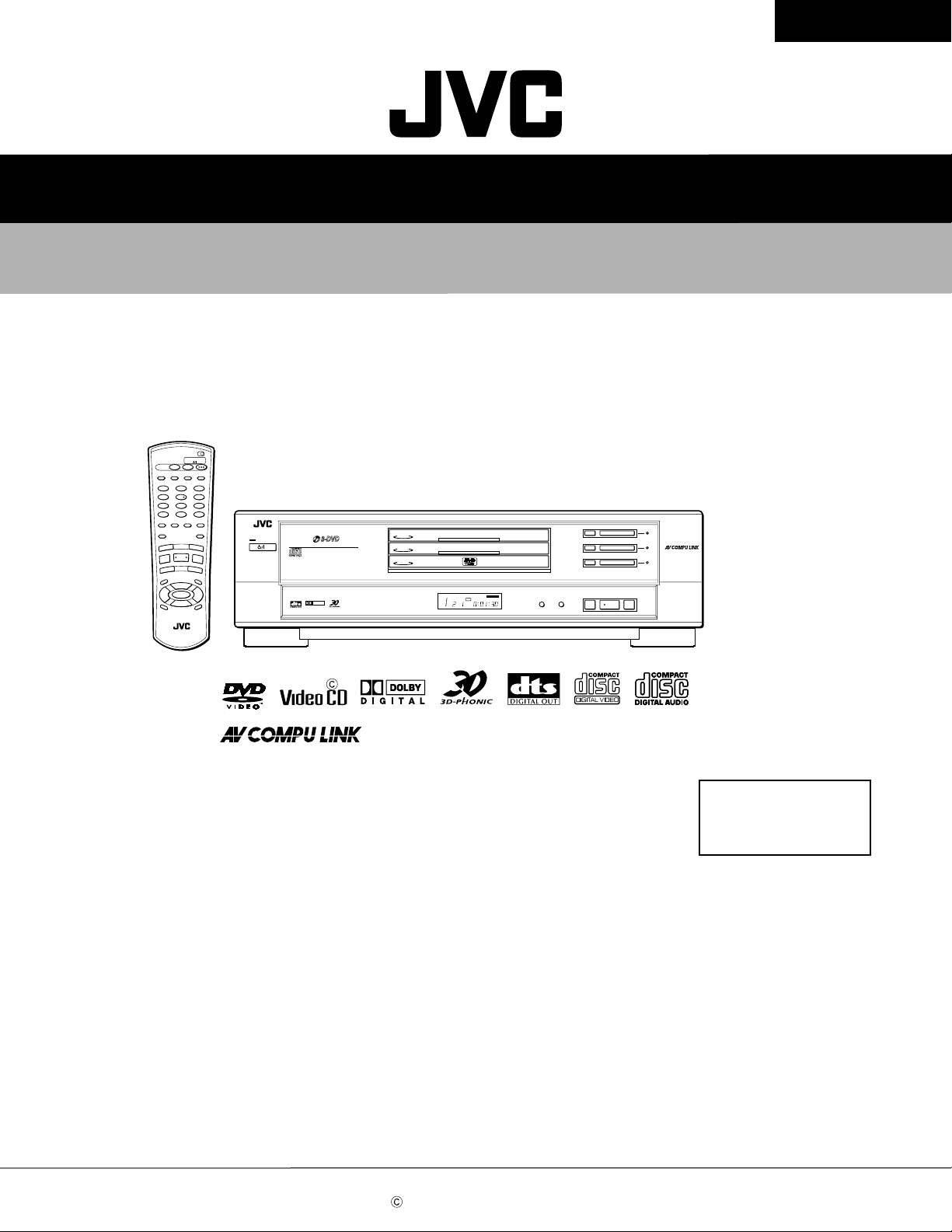
SERVICE MANUAL
DVD VIDEO PLAYER
XV-M50BK
TV DVD
STANDBY/ON
DISC
SELECT
TV DVD
PLAY
3D
TV/VIDEO
MODE
PHONIC
CANCEL
RETURN
TV1 TV2 TV3
123
TV4 TV5 TV6
4
56
TV7 TV8 TV9
89
7
TV
-/-- TV0 MUTING
0+1010
THEATER
POSITION
SUBTITLEANGLE
AUDIO
DIGEST
S
U
IO
V
E
R
P
SELECT
R
A
E
L
C
–
W
O
L
S
E
L
T
I
T
+
CH
VOL
-
ENTER
C
-
CH
H
O
I
C
E
RM-SXVM50J REMOTE CONTROL
ZOOM
N
E
X
T
S
T
R
O
B
E
S
L
O
W
+
M
E
N
U
VOL
+
Y
A
L
P
S
I
D
STANDBY
STANDBY/ON
PLAY & EXCHANGE
DVD / VIDEO CD / CD
10-bit/27MHz VIDEO D/A CONVERTER
DOLBY
D I G I T A L
3
DISC
2
DISC
1
DISC
XV-M50 DVD/CD PLAYER
DISC TITLE CHAP RESUME THEATER
DVD
EACH
SKIP
DISC 3
3
DISC 2
2
DISC 1
1
PAUSEPLAYSTOP
XV-M50BK
Contents
Safety precautions ------------------------ 1-2
Preventing static electricity ------------- 1-3
Precautions for Service ------------------ 1-4
Importance admistering point
on the safety ----- 1-5
COPYRIGHT 2001 VICTOR COMPANY OF JAPAN, LTD.
Area Suffix
J ------------- U.S.A.
C ---------- Canada
Disassembly method -------------------- 1-6
Adjustment method ----------------------- 1-21
Description of major ICs ---------------- 1-25
No.A0008
Jun. 2001
Page 2
XV-M50BK
1. This design of this product contains special hardware and many circuits and components specially
for safety purposes. For continued protection, no changes should be made to the original design
unless authorized in writing by the manufacturer. Replacement parts must be identical to those
used in the original circuits. Services should be performed by qualified personnel only.
2. Alterations of the design or circuitry of the product should not be made. Any design alterations of
the product should not be made. Any design alterations or additions will void the warranty
and will further relieve the manufacture of responsibility for personal injury or property damage
resulting therefrom.
3. Many electrical and mechanical parts in the products have special safety-related characteristics.
These characteristics are often not evident from visual inspection nor can the protection afforded
by them necessarily be obtained by using replacement components rated for higher voltage,
wattage, etc. Replacement parts which have these special safety characteristics are identified in
the Parts List of Service Manual. Electrical components having such features are identified by
shading on the schematics and by ( ) on the Parts List in the Service Manual. The use of a
substitute replacement which does not have the same safety characteristics as the recommended
replacement parts shown in the Parts List of Service Manual may create shock, fire, or other
hazards.
4. The leads in the products are routed and dressed with ties, clamps, tubings, barriers and the
like to be separated from live parts, high temperature parts, moving parts and/or sharp edges
for the prevention of electric shock and fire hazard. When service is required, the original lead
routing and dress should be observed, and it should be confirmed that they have been returned
to normal, after reassembling.
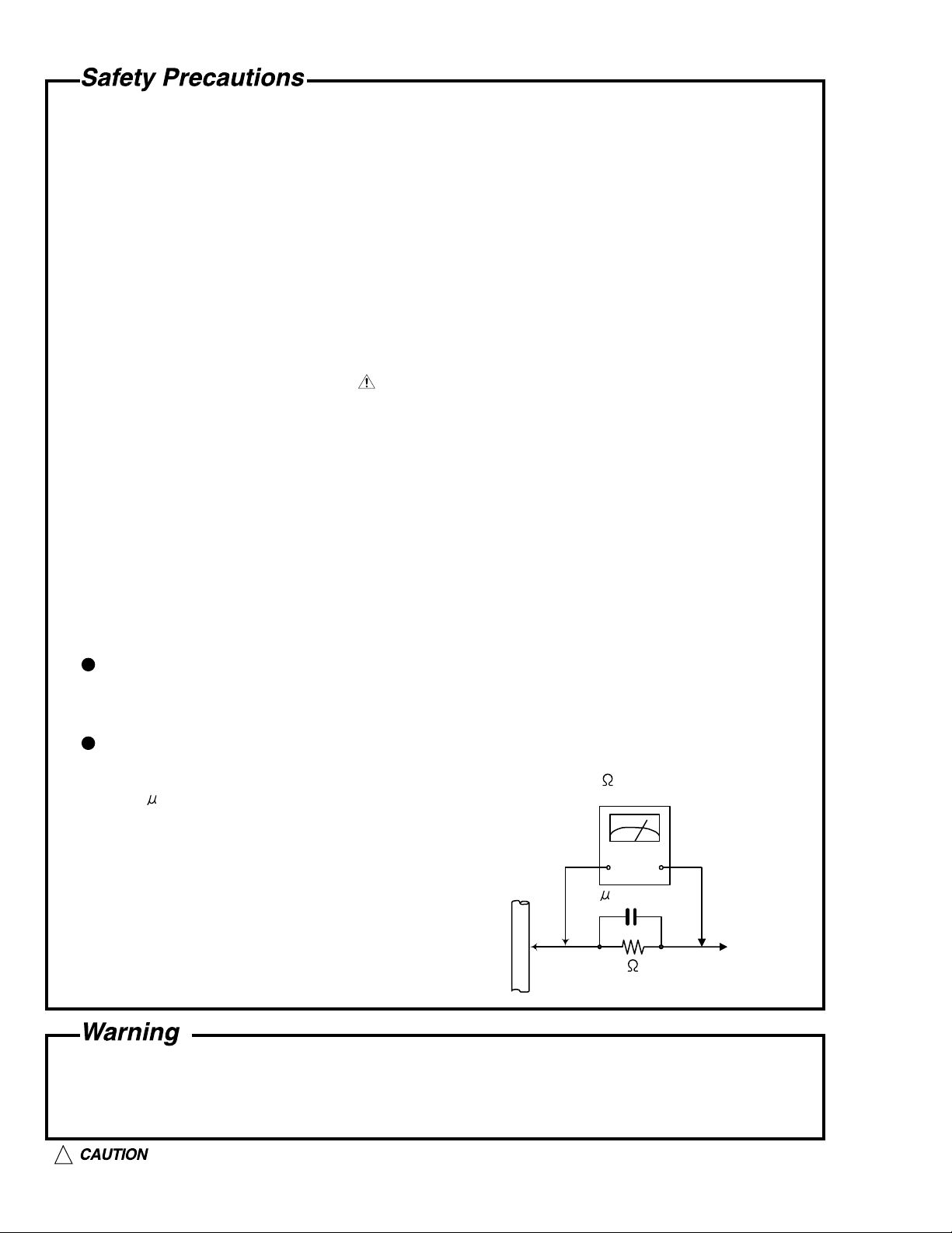
5. Leakage current check (Electrical shock hazard testing)
After reassembling the product, always perform an isolation check on the exposed metal parts of
the product (antenna terminals, knobs, metal cabinet, screw heads, headphone jack, control
shafts, etc.) to be sure the product is safe to operate without danger of electrical shock.
Do not use a line isolation transformer during this check.
Plug the AC line cord directly into the AC outlet. Using a "Leakage Current Tester", measure
the leakage current from each exposed metal parts of the cabinet , particularly any exposed
metal part having a return path to the chassis, to a known good earth ground. Any leakage
current must not exceed 0.5mA AC (r.m.s.)
Alternate check method
Plug the AC line cord directly into the AC outlet. Use an AC voltmeter having, 1,000 ohms
per volt or more sensitivity in the following manner. Connect a 1,500 10W resistor paralleled by
a 0.15 F AC-type capacitor between an exposed
metal part and a known good earth ground.
Measure the AC voltage across the resistor with the
AC voltmeter.
AC VOLTMETER
(Having 1000
ohms/volts,
or more sensitivity)
Move the resistor connection to each exposed
metal part, particularly any exposed metal part
having a return path to the chassis, and measure
the AC voltage across the resistor. Now, reverse
the plug in the AC outlet and repeat each
measurement. voltage measured Any must not
0.15 F AC TYPE
1500 10W
Place this
probe on
each exposed
metal part.
exceed 0.75 V AC (r.m.s.). This corresponds to 0.5
Good earth ground
1. This equipment has been designed and manufactured to meet international safety standards.
2. It is the legal responsibility of the repairer to ensure that these safety standards are maintained.
3. Repairs must be made in accordance with the relevant safety standards.
4. It is essential that safety critical components are replaced by approved parts.
5. If mains voltage selector is provided, check setting for local voltage.
!
Burrs formed during molding may be left over on some parts of the chassis. Therefore,
pay attention to such burrs in the case of preforming repair of this system.
1-2
Page 3
XV-M50BK
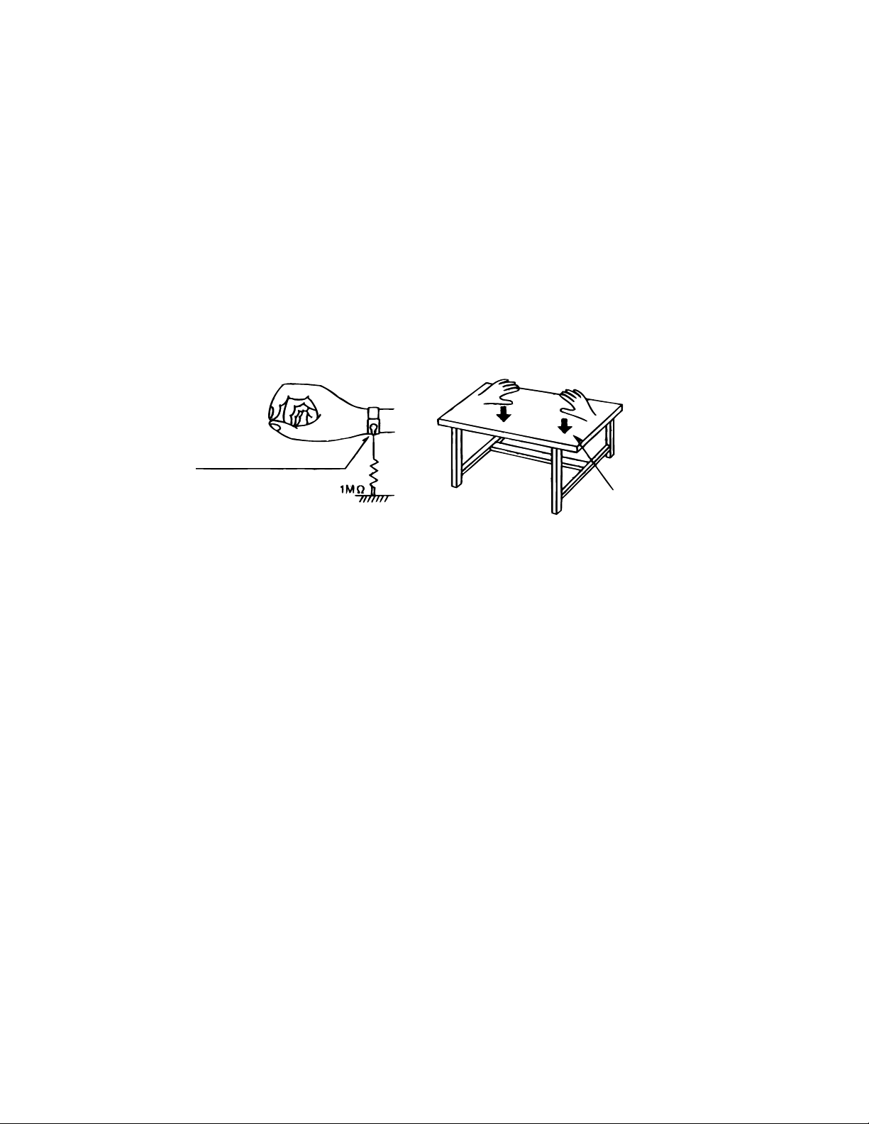
Preventing static electricity
Electrostatic discharge (ESD), which occurs when static electricity stored in the body, fabric, etc. is discharged,
can destroy the laser diode in the traverse unit (optical pickup). Take care to prevent this when performing repairs.
1.1. Grounding to prevent damage by static electricity
Static electricity in the work area can destroy the optical pickup (laser diode) in devices such as DVD players.
Be careful to use proper grounding in the area where repairs are being performed.
1.1.1. Ground the workbench
1. Ground the workbench by laying conductive material (such as a conductive sheet) or an iron plate over
it before placing the traverse unit (optical pickup) on it.
1.1.2. Ground yourself
1. Use an anti-static wrist strap to release any static electricity built up in your body.
(caption)
Anti-static wrist strap
Conductive material
(conductive sheet) or iron plate
1.1.3. Handling the optical pickup
1. In order to maintain quality during transport and before installation, both sides of the laser diode on the
replacement optical pickup are shorted. After replacement, return the shorted parts to their original condition.
(Refer to the next page.)
2. Do not use a tester to check the condition of the laser diode in the optical pickup. The tester's internal power
source can easily destroy the laser diode.
1.2. Handling the traverse unit (optical pickup)
1. Do not subject the traverse unit (optical pickup) to strong shocks, as it is a sensitive, complex unit.
2. For specific details, refer to the replacement procedure in the text. Be careful not to take too long a time
when attaching it to the connector.
3. Handle the flexible cable carefully as it may break when subjected to strong force.
4. It is not possible to adjust the semi-fixed resistor that adjusts the laser power. Do not turn it
1-3
Page 4
XV-M50BK
Precautions for Service
Handling of Traverse Unit and Laser Pickup
1. Do not touch any peripheral element of the pickup or the actuator.
2. The traverse unit and the pickup are precision devices and therefore must not be subjected to
strong shock.
3. Do not use a tester to examine the laser diode. (The diode can easily be destroyed by the
internal power supply of the tester.)
4. When replacing the pickup, after mounting a new pickup, remove the solder on the short land
which is provided at the center of the flexible wire to open the circuit.
5. Half-fixed resistors for laser power adjustment are adjusted in pairs at shipment to match the
characteristics of the optical block.
Do not change the setting of these half-fixed resistors for laser power adjustment.
Destruction of Traverse Unit and Laser Pickup by Static Electricity
Laser diodes are easily destroyed by static electricity charged on clothing
or the human body. Before repairing peripheral elements of the traverse
unit or pickup, be sure to take the following electrostatic protection:
1. Wear an antistatic wrist wrap.
2. With a conductive sheet or a steel plate on the workbench on which
the traverse unit or the pick up is to be repaired, ground the sheet
or the plate.
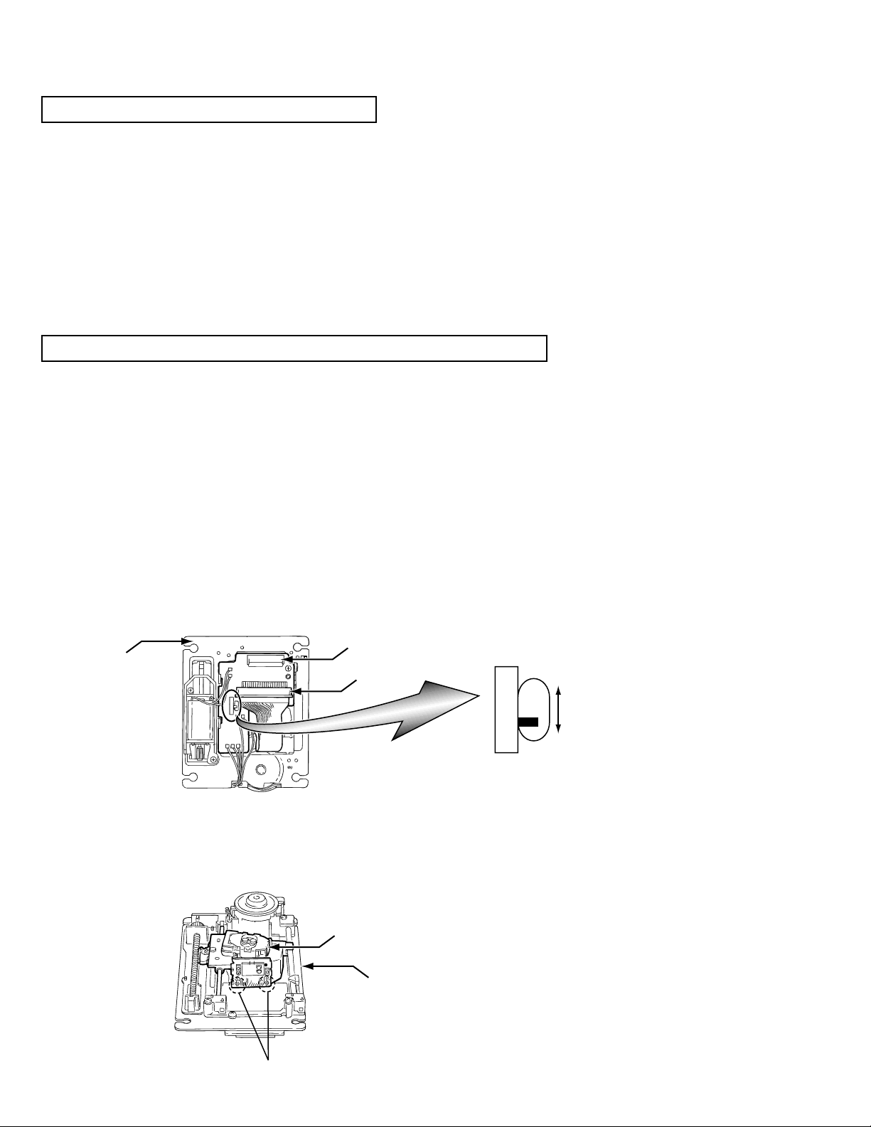
When you remove the traverse mechanism from the servo control substrate
The laser diode of pick-up might be destroyed by static electricity and set switch (S11) on the pick-up board
on "SHORT" side, please before removing the card wire from connector (CN10).
Moreover, please set switch (S11) on "OPEN" side after assembling and inserting the card wire in
connector (CN10) without fail at times.
Traverse
mechanism
CN10
CN12
SWITCH S11
SHORT
OPEN
When you remove the pick-up from the traverse mechanism
The laser diode of the pick-up might be destroyed by static electricity, and solder with part a, please before
extracting a flexible wire from connector (CN12).
Moreover, please remove solder in part a after inserting a flexible wire in connector (CN12).
1-4
Pick-up
Traverse
mechanism
Soldering part
Page 5
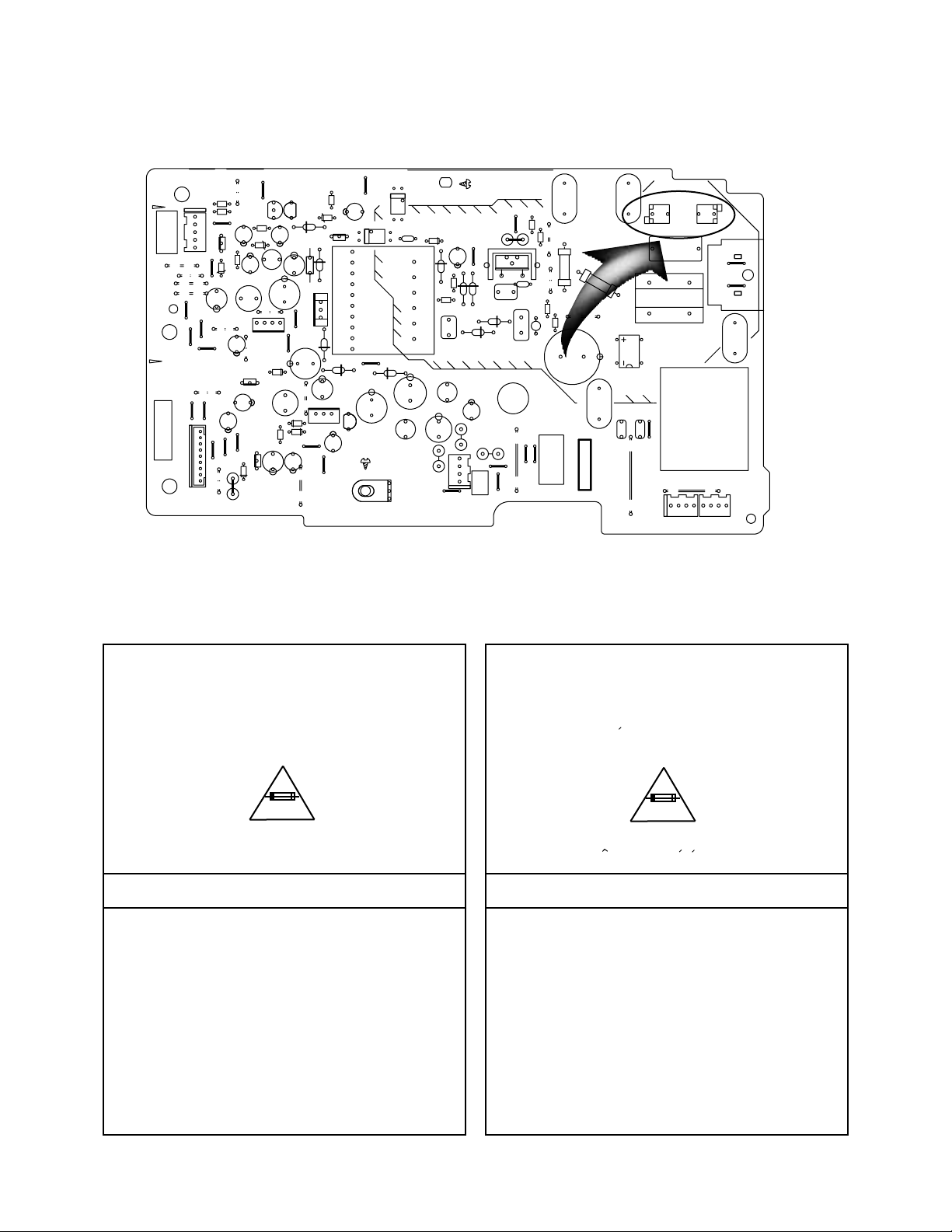
Importance Admistering point on the Safety
F901
D954
D991
IC953
R960
D952
T901
B9015
Q991
D956
C978
C992
CP952
EP951
B9016
B9017
PC901
C982
PC902
L957
D957
C918
C987
L959
C984
K952
D911
C909
D910
R903
K953
CN981
B9018
C914
R904
C989
D908
D902
D904
B9030
C913
D903
K951
K902
B9024
HS901
B9019
B9020
B9023
IC901
C908
S1B
B9601
R908
C915
B9021
R906
R901
LEA10018-
B9022
A1
C906
B9111
B9206
R907
R910
R911
C907
B9207
C916
C905
C912
1.6A/125V
FC902
C902
L901
D901
C911
B9025
B9801
B9501
B9201
B9102
B9202
B9203
CN971
B9031
B9005
B9008
B9004
B9006
B9113
CN961
B9003
C966
B9007
B9029
R957
B9002
Q953
D950
B9104
B9107
C969
B9001
B9013
B9101
R956
C962
R980
B9028
K954
L952
C974
C964
C973
D974
B9106
Q965
B9010
R953
D960
IC951
Q966
Q951
C965
B9105
D970
L955
R976
C995
L951
C979
CP951
C960
B9011
B9012
D973
D972
C963
R954
B9204
C996
B9301
D951
D953
C997
B9014
F901
FC901
XV-M50BK
P901
B9026
B9027
C904
CN952 CN951
Full Fuse Replacement Marking
Graphic symbol mark
(This symbol means fast blow type fuse.)
should be read as follows ;
FUSE CAUTION
FOR CONTINUED PROTECTION AGAINST RISK
OF FIRE, REPLACE ONLY WITH SAME TYPE
AND RATING OF FUSES ;
F901 : 1.6 A / 125 V
Marquage Pour Le Remplacement
Complet De Fusible
Le symbole graphique (Ce symbole signifie
fusible de type a fusion rapide.)
doit etre interprete comme suit ;
PRECAUTIONS SUR LES FUSIBLES
POUR UNE PROTECTION CONTINUE CONTRE
DES RISQUES D'INCENDIE, REMPLACER
SEULEMENT PAR UN FUSIBLE DU MEME TYPE ;
F901 : 1.6 A / 125 V
1-5
Page 6
XV-M50BK
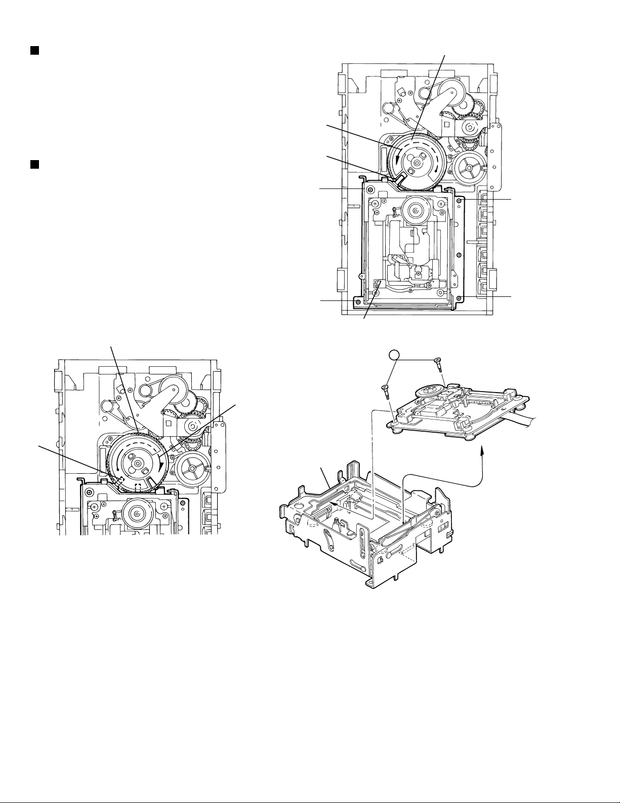
Disassembly method
<
Main body
Removing the top cover (See Fig.1)
1.
Remove the two screws A attaching the top cover
on the back of the body.
2.
Remove the four screws B attaching the top cover
on both sides of the body.
3.
Pull the lower parts of the top cover sides and
remove the top cover in the direction of the arrow.
Removing the front panel assembly
Prior to performing the following procedure, remove
the top cover.
1.
Disconnect the wire from connector CN971 on the
power supply board.
>
(See Fig.2 to 5)
Top cover
B
2
Power supply board
CN971
B
A
2
Fig.1
System control board
CN703
2.
Disconnect the card wire from connector CN703 on
the system control board.
3.
Remove the three screws C attaching the front
panel assembly on the bottom of the body.
4.
Release the joint a on the bottom and the two joints
b on both sides of the body. Remove the front panel
assembly toward the front.
Front panel assembly
C
Front panel assembly
Fig.2
Joint a
C
Fig.3
Front panel assembly
C
1-6
Joint b
Joint b
Fig.5Fig.4
Page 7

XV-M50BK
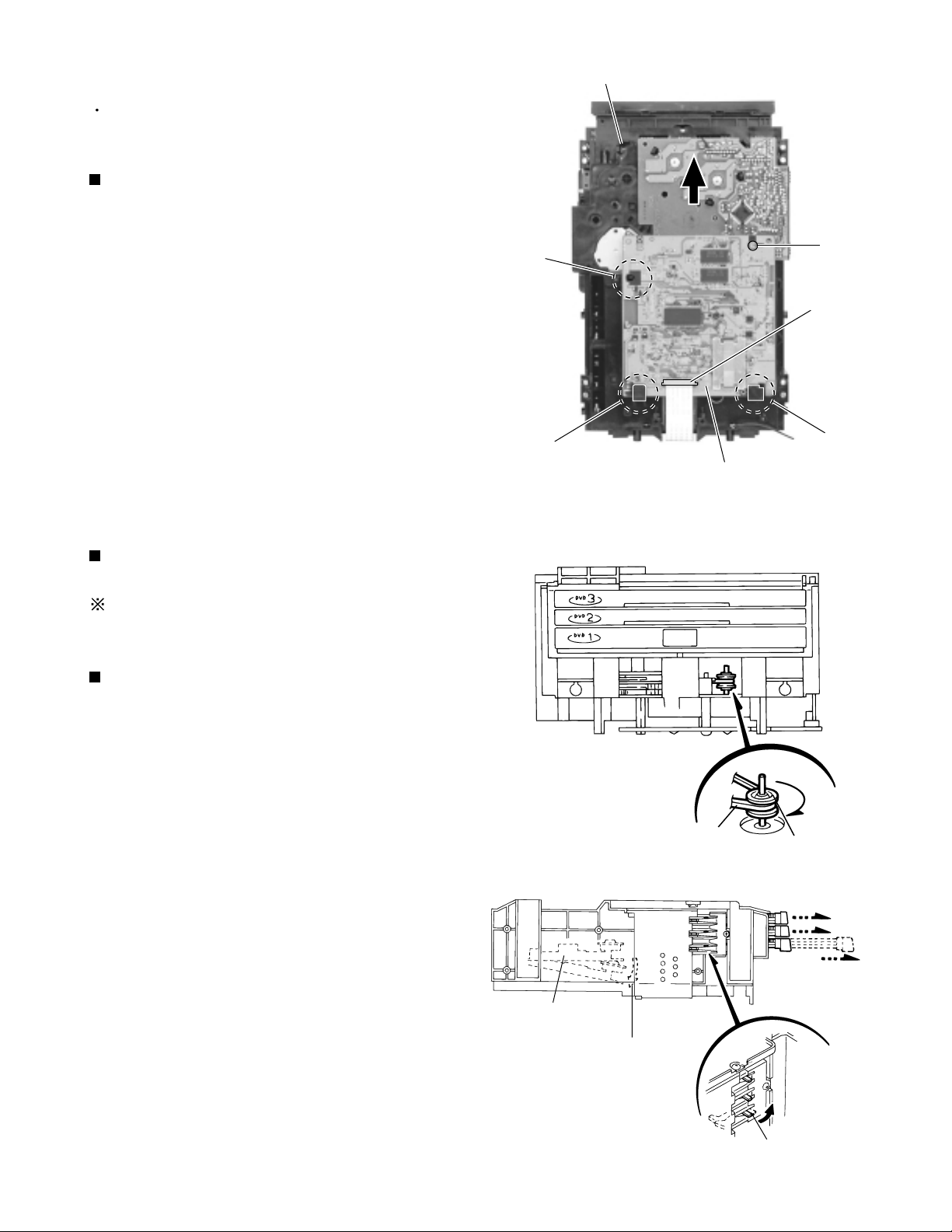
Removing the rear panel (See Fig.6)
Prior to performing the following procedure, remove
the top cover.
1.
Remove the eleven screws D attaching the rear
panel on the back of the body and detach the rear
panel.
Removing the DVD changer mechanism assembly
(See Fig.7)
Prior to performing the following procedure, remove
the top cover and front panel assembly.
1.
Remove the one screw E.
2.
Disconnect the 9 pin wire from connector CN961 on
the power supply board.
D
D
Power supply board
F
Fig.6
F
E
Rear panel
D
Video board
CN601
CN701
System control
board
3.
Disconnect the card wire from connector CN601 on
the video board.
4.
Disconnect the card wires from connector CN701
and CN702 on the system control board.
5.
Remove the four screws F attaching the DVD
changer mechanism assembly.
It is easy for removing the front panel assembly to
remove the mechanism assembly though the
mechanism assembly can be removed even in the
state that the front panel assembly adheres.
CN961
F
DVD changer mechanism assembly
F
Fig.7
CN702
1-7
Page 8
XV-M50BK
Removing the power supply board
(See Fig.8 and 9)
Prior to performing the following procedure, remove
the top cover.
1.
Disconnect the wire from connector CN971 on the
power supply board (The wire is extending from the
front panel assembly).
2.
Disconnect the 9 pin wire from connector CN961 on
the power supply board (The wire is extending from
the DVD changer mechanism assembly).
3.
Disconnect the wire from connector CN951 and
CN952 on the power supply board (The wire is
extending from the system control board).
4.
Remove the screw D attaching the AC jack on the
rear panel.
5.
Remove the two screws G attaching the power
supply board and detach the power supply board.
Power supply board
G
CN971
CN961
Rear panel
CN951,CN952
Front panel assembly
Fig.8
Rear panel
Fig.9
D
1-8
Page 9
XV-M50BK
Removing the video board
(See Fig.10 and 11)
Prior to performing the following procedure, remove
the top cover.
1.
Disconnect the card wire from connector CN601 on
the video board (The card wire is extending from the
DVD changer mechanism assembly).
2.
Disconnect the wire from connector CN704 on the
system control board (The wire is extending from the
video board).
3.
Remove the three screws D attaching the video
board on the rear panel. Pull out the video board
from the rear panel.
Removing the system control board
(See Fig.12 and 13)
Prior to performing the following procedure, remove
the top cover.
The system control board can be removed even if
the video board is attached.
1.
Disconnect the card wire from connector CN703 on
the system control board (The card wire is extending
from the front panel assembly).
Rear panel
Front panel assembly
D
Power supply board
CN951,CN952
Fig.10
Rear panel
Fig.11
Rear panel
CN601
CN704
Video board
CN704
System control
board
Video board
CN701
2.
Disconnect the card wire from connector CN701 and
CN702 on the audio board (The card wires are
extending from the DVD changer mechanism
assembly).
3.
Disconnect the wire from connector CN704 on the
system control board (The wire is extending from the
video board).
4.
Disconnect the wire from connector CN951 and
CN952 on the power supply board (The wire is
extending from the system control board).
5.
Remove the screw H attaching the system control
board.
6.
Remove the four screws D attaching the system
control board on the rear panel. Pull out the system
control board toward the front.
Front panel assembly
D
Fig.12
Rear panel
Fig.13
CN703
H
System control
board
CN702
1-9
Page 10
XV-M50BK
<
Front panel assembly
Prior to performing the following procedure, remove
the top cover and the front panel assembly.
>
Removing the front board
(See Fig.14 and 15)
1.
Remove the two screws I on the back of the front
panel assembly and remove the bracket from the
front panel assembly.
2.
Remove the seven screws J attaching the front
board.
If necessary, unsolder FW803 and disconnect the
wire.
Removing the STANDBY switch board
(See Fig.16)
1.
Remove the two screws K on the back of the front
panel assembly.
Front panel assembly
Front board
J
Front board
Bracket
I
Fig.14
I
J
J
FW803
Fig.15
K
If necessary, unsolder FW803 and disconnect the
wire.
FW803
STANDBY switch board
Fig.16
1-10
Page 11
XV-M50BK
<
DVD changer mechanism assembly
Prior to performing the following procedure, remove
the top cover and the DVD changer mechanism
assembly.
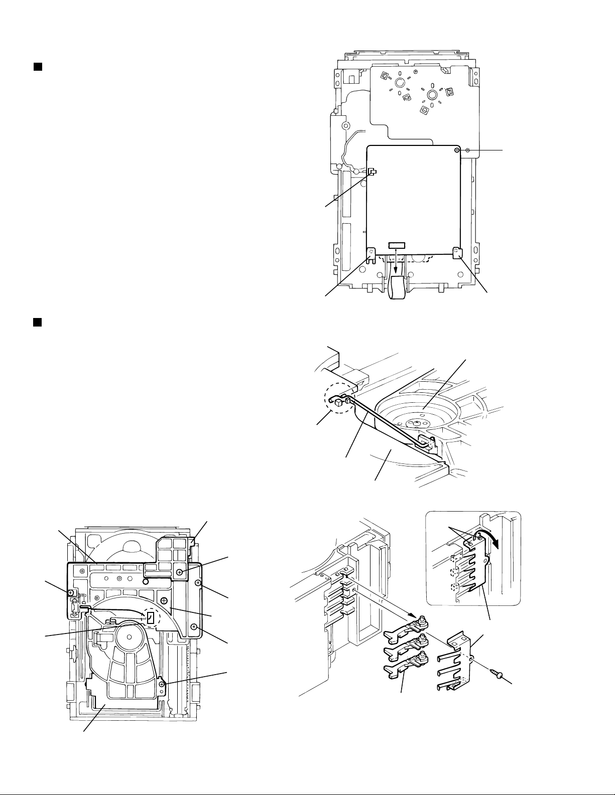
Removing the traverse mechanism
control board (See Fig.17)
1.
Disconnect the card wire from connector CN101 on
the traverse mechanism control board on the bottom
of the DVD changer mechanism assembly.
2.
Remove the screw L attaching the traverse
mechanism control board. Release the three parts e,
f and g and remove the traverse mechanism control
board.
Ejecting the DVD (See Fig.18 and 19)
DVD changer mechanism assembly
>
Par t
e
Par t
f
Fig.17
L
CN101
Par t
DVD traverse
mechanism control board
g
When the DVD is set or the traverse
mechanism is up.
The DVD tray can not be ejected when the traverse
mechanism is up.
Bringing down the traverse mechanism
as shown in the Fig.20
1.
The motor pulley and the belt can be seen on the
front side of the changer. Turn the motor pulley
clockwise until the belt stops.
2.
Pull the tray lock lever on the left side of the changer
and draw the DVD tray.
3.
Draw the DVD tray 1 to 3 as above.
Fig.18
Belt
Motor pulley
Draw the DVD tray.
Traverse mechanism
As the motor pulley is
turned, the traverse
mechanism lowers.
Fig.19
Tray stopper
Tray lock lever
1-11
Page 12
XV-M50BK
<
DVD Changer Mechanism Section
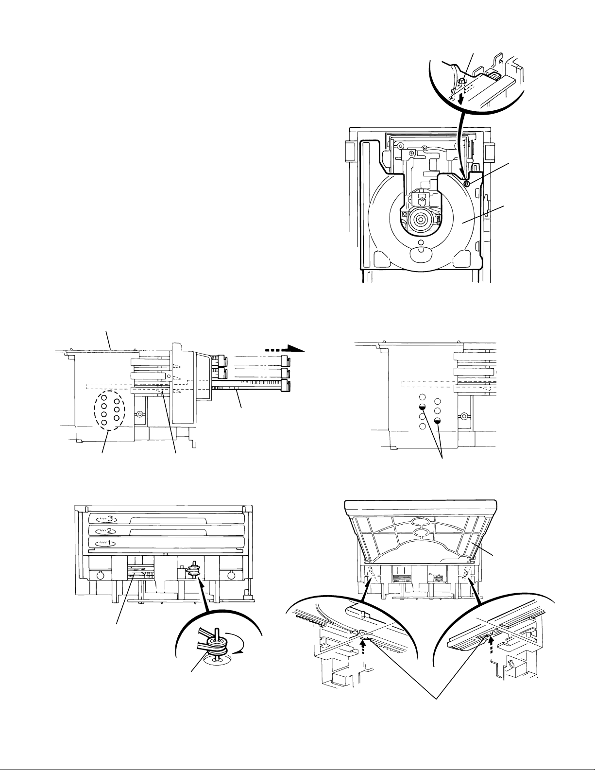
Removing the DVD mechanism board
(See Fig.1)
1.
Remove the DVD changer mechanism assembly.
2.
From bottom side the DVD changer mechanism
assembly, remove the one screw A retaining the DVD
servo control board.
Disconnect the card wire from the connector CN101 on
3.
the DVD servo control board.
Disengage the one engagement a and two
4.
engagements b , remove the DVD servo control board.
ATTENTION !
The laser diode of pick-up might be destroyed by static
electricity and set switch (S11) on the pick-up board on
"SHORT" side, please before removing the card wire from
connector (CN101).
Moreover, please set switch (S11) on "OPEN" side after
assembling and inserting the card wire in connector (CN101)
without fail at times.
Please refer to page 1-4 for a detailed content.
>
A
DVD servo
control board
a
CN101
bb
Removing the DVD tray assembly
(See Fig.2~4)
Remove the screw B retaining the Disc stopper
1.
(See Fig.3).
Remove the three screws C retaining the T.bracket
2.
(See Fig.3).
From the clamper base section c, remove both of the
3.
edges fixing the rod(See Fig.2 and 3).
Remove the screw D retaining the clamper assembly
4.
(See Fig.3).
From the left side face of the chassis assembly, remove
5.
the one screw E retaining both of the return spring and
lock lever(See Fig. 4).
By removing the pawl at the section d fixing the return
6.
spring, dismount the return spring(See Fig.4).
Remove the three lock levers(See Fig.4).
7.
Disc stopper
T.Bracket
B
C
C
Lod stopper
(C/J version only)
c
C
Fig.1
Clamper base
c
Rod
T.Bracket
Fig.2
d
Return spring
Clamper assembly
1-12
D
E
Lock lever
Fig.4
Fig.3
Page 13
XV-M50BK
8.9.Check whether the lifter unit stopper has been caught
into the hole at the section e of DVD tray assembly as
shown in Fig.5.
Make sure that the driver unit elevator is positioned as
shown in Fig.6 from to the second or fifth hole on the
left side face of the DVD Traverse mechanism
assembly.
[Caution]
10.
11.
12.
Chassis assembly
In case the driver unit elevator is not at above
position, set the elevator to the position as
shown in Fig.7 by manually turning the pulley
gear as shown in Fig.8.
Manually turn the motor pulley in the clockwise
direction until the lifter unit stopper is lowered from the
section e of DVD tray assembly(See Fig.8).
Pull out all of the three stages of DVD tray assembly in
the arrow direction f until these stages stop
(See Fig.6).
At the position where the DVD tray assembly has
stopped, pull out the DVD tray assembly while
pressing the two pawls g and g' on the back side of
DVD tray assembly(See Fig.9). In this case, it is easy
to pull out the assembly when it is pulled out first from
the stage DVD tray assembly.
Stopper
e
DVD tray
assembly
Fig.5
Refer to Fig.7
Pulley gear
Pawl
DVD tray assembly
g
f
Drive unit of elevator
Fig.7Fig.6
DVD tray assembly
Fig.8
Motor pulley
Fig.9
Pawl ,
g
g'
1-13
Page 14
XV-M50BK
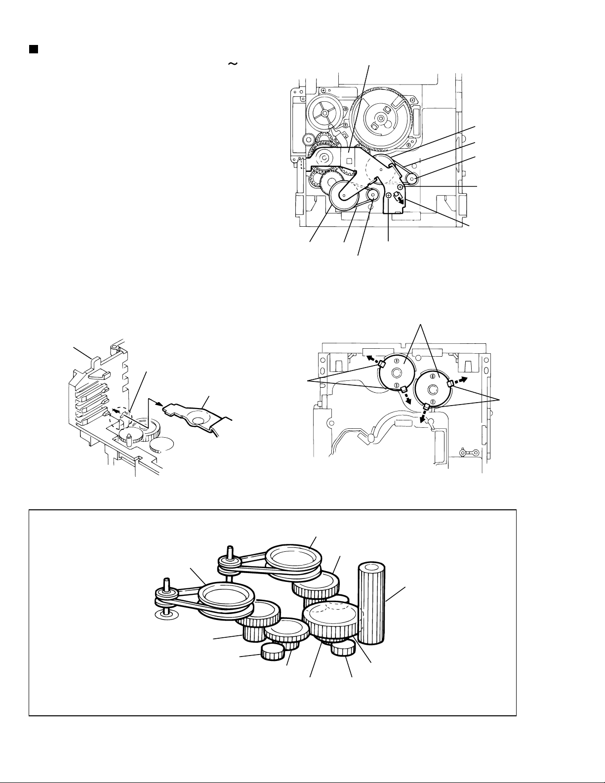
Removing the DVD mechanism
Cams R1, R2 assembly
assembly(See Fig.10)
1.2.While turning the cams R1 and R2 assembly in the
arrow direction h , align the shaft i of the DVD
mechanism assembly to the position shown in Fig.10.
Remove the four screw F retaining the DVD
mechanism assembly.
Arrow
h
i
Removing the DVD traverse mechanism
assembly (See Fig.11 and 12 )
F
For dismounting only the DVD mechanism without
1.
removing the DVD mechanism assembly, align the shaft
j of the DVD mechanism assembly to the position
shown Fig.11 while turning the cam R1 and R2
assembly in the arrow direction k.
Remove the two screws G raising the DVD mechanism
2.
assembly.
Remove the DVD traverse mechanism assembly in the
3.
arrow direction I from the lifter unit (See Fig. 12)
F
DVD mechanism assembly
Cam R1, R2 assembly
Fig.10
G
F
F
DVD traverse
mechanism
assembly
Arrow
k
j
Lifter unit
Fig.11
Fig.12
Arrow
l
1-14
Page 15
Removing the mechanism control
board (See Fig.14, 15)
1.
Absorb the four soldered positions m of the right and
left motors with a soldering absorber(See Fig.14).
2.
Remove the two screws H retaining the mechanism
control board(See Fig.14).
Remove the two screws I retaining the tray select
3.
switch board(See Fig.15).
Removing the cam unit
(See Fig.15 18 )
1.
Remove the DVD mechanism assembly.
2.
While turning the cam gear L, align the pawl n position
of the drive unit to the notch position(Fig.15) on the cam
gear L.
Pull out the drive unit and cylinder gear(See Fig.17).
3.
While turning the cam gear L, align the pawl o position
4.
of the select lever to the notch position(Fig.18) on the
cam gear L.
Remove the four screws J retaining the cam unit(cam
5.
gear L and cams R1/R2 assembly)(See Fig.18).
m
Motor L
Mechanism control board
H
Fig.14
XV-M50BK
Motor R
m
H
Chassis assembly
CN801
Fig.15
CN802
Drive unit
CD Tray
switch board
Cylinder gear
CN804
Drive unit
n
I
Cam gear L
J
Cam gear L
Fig.16
Cams R1, R2 assembly
J
Cam unit
J
Fig.17
o
Select lever
Fig.18
1-15
Page 16
XV-M50BK
Removing the actuator motor and belt
(See Fig.19 22)
1.
Remove the two screws K retaining the gear bracket
(See Fig.19).
2.
While pressing the pawl p fixing the gear bracket in the
arrow direction, remove the gear bracket
(See Fig.19).
From the notch q section on the chassis assembly fixing
3.
the edge of gear bracket, remove and take out the gear
bracket(See Fig. 20).
Remove the belts respectively from the right and left
4.
actuator motor pulleys and pulley gears(See Fig. 19).
After turning over the chassis assembly, remove the
5.
actuator motor while spreading the four pawls r fixing
the right and left actuator motors in the arrow
direction(See Fig. 21).
[Note]
When the chassis assembly is turned over under
the conditions wherein the gear bracket and belt
have been removed, then the pulley gear as well
as the gear, etc. constituting the gear unit can
possibly be separated to pieces. In such a case,
assemble these parts by referring to the assembly
and configuration diagram in Fig. 22.
Pulley gear
Gear bracket
Belt
Motor pulley
K
Fig.19
Actuator motor
Pulley gear
Belt
Motor pulley
K
Pawl
p
Chassis assembly
q
Gear bracket
Fig.20
Assembly and Configuration Diagram
Pulley gear
r
r
Fig.21
Pulley gear
Gear B
Cylinder gear
1-16
Gear B
Gear C
Select gear
Gross gear L
Fig.22
Gross gear U
Gear C
Page 17
XV-M50BK
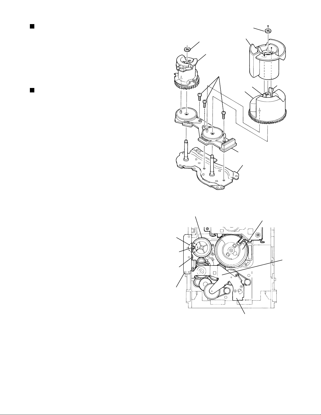
Removing the cams R1/R2 assembly
and cam gear L (See Fig.23)
Remove the slit washer fixing the cams R1 and R2
1.
assembly.
By removing the two pawls s fixing the cam R1,
2.
separate R2 from R1.
Remove the slit washer fixing the cam gear L.
3.
Pull out the cam gear L from the C.G. base assembly.
4.
Removing the C.G. base assembly
(See Fig.23 and 24)
Remove the three screws L retaining the C.G. base
assembly.
[Caution]
To reassemble the cylinder gear, etc.with the
R1/R2
cam unit (cam gear and cams
gear unit and drive unit, align the position of the
pawl n on the drive unit to that of the notch on
the cam gear L. Then, make sure that the gear
unit is engaged by turning the cam gear L
(See Fig. 24).
assembly),
Slit washer
Cam gear L
L
Slit washer
Cam R2
s
Pawl
Cam R1
Cam switch board
C.G. base assembly
Pawl
s
Notch
Pawl
n
Cylinder
gear
Drive unit
Fig.23
Cam gear L
Cam R1, R2 assembly
Gear unit
Gear bracket
Fig.24
1-17
Page 18

XV-M50BK
< DVD Traverse mechanism section>
Removing the pickup (See Fig.1 to 5)
1.
Solder soldering a on the flexible board next to the
pickup unit.
2.
From the bottom of the traverse mechanism unit,
disconnect the flexible wire from CN12 on the pickup
board.
ATTENTION
The laser diode of the pick-up might be destroyed by
static electricity, and solder with part a, please before
extracting a flexible wire from connector (CN12).
Moreover, please remove solder in part a after
inserting a flexible wire in connector (CN12).
Please refer to page 1-4 for a detailed content.
3.
Remove the screw A attaching the shaft stopper (R)
on the upper side of the traverse mechanism unit.
Pull the side of the shaft stopper (R) outward to
release the joint b and remove it upward. Remove
the skew spring at the same time.
Pickup unit
Flexible board
a
Fig.1
Pickup board
CN12
Flexible wire
4.
Move the shaft in the direction of the arrow to release
it from the part c.
5.
Release the joint d with the shaft and remove the
pickup with the shaft.
6.
Pull out the shaft.
7.
Remove the screw B attaching the switch actuator.
Shaft
Pickup
B
Pickup unit
Shaft
Joint d
Shaft stopper (R)
Fig.2
Shaft stopper (R)
Fig.3
A
A
Part c
Shaft
Shaft stopper (R)
Joint b
1-18
Switch actuator
Skew spring
Shaft
Fig.4Fig.5
Page 19

Removing the pickup board
(See Fig.1 and 6)
1.
Solder soldering a on the flexible board next to the
pickup unit.
2.
From the bottom of the traverse mechanism unit,
disconnect the flexible wire from CN12 on the pickup
board.
ATTENTION
The laser diode of the pick-up might be destroyed by
static electricity, and solder with part a, please before
extracting a flexible wire from connector (CN12).
Moreover, please remove solder in part a after
inserting a flexible wire in connector (CN12).
Please refer to page 1-4 for a detailed content.
3.
Unsolder soldering e, f and g of each harness on the
pickup board.
XV-M50BK
Pickup unit
Flexible board
a
Fig.1
e
Pickup board
4.
Remove the screw C attaching the pickup board and
release the two joints h.
Removing the feed motor assembly
(See Fig.1, 6 and 7)
1.
Solder soldering a on the flexible board next to the
pickup unit.
2.
From the bottom of the traverse mechanism unit,
disconnect the flexible wire from CN12 on the pickup
board.
ATTENTION
The laser diode of the pick-up might be destroyed by
static electricity, and solder with part a, please before
extracting a flexible wire from connector (CN12).
Moreover, please remove solder in part a after
inserting a flexible wire in connector (CN12).
Please refer to page 1-4 for a detailed content.
3.
Unsolder soldering e of the motor harness on the
pickup board.
Joint h
Joint h
Feed motor assembly
C
CN12
f
g
Fig.6
Feed motor assembly
Thrust spring
D
D
4.
Remove the two screws D attaching the feed motor
assembly and remove the thrust spring. Move the
feed motor assembly in the direction of the arrow to
pull it out from the feed holder.
Feed holder assembly
Fig.7
1-19
Page 20

XV-M50BK
Removing the turn table assembly
(See Fig.1, 6, 8 and 9)
1.
Solder soldering a on the flexible board next to the
pickup unit.
2.
From the bottom of the traverse mechanism unit,
disconnect the flexible wire from CN12 on the pickup
board.
ATTENTION
The laser diode of the pick-up might be destroyed by
static electricity, and solder with part a, please before
extracting a flexible wire from connector (CN12).
Moreover, please remove solder in part a after
inserting a flexible wire in connector (CN12).
Please refer to page 1-4 for a detailed content.
3.
Unsolder soldering f and g of the harness extending
from the turn table assembly to the pickup board.
4.
Remove the screw E attaching the shaft stopper (F)
on the upper side of the traverse mechanism unit.
Pull the side of the shaft stopper (F) outward to
release the joint i and remove it upward. Remove the
spring at the same time.
5.
Remove the screw F attaching the turn table
assembly.
Joint h
Joint h
Feed motor assembly
Pickup unit
Flexible board
a
Fig.1
e
Pickup board
C
CN12
f
g
Fig.6
6.
Move the turn table assembly outward and pull out
from the shaft. Then remove it from the base chassis.
Shaft stopper (F)
Shaft stopper (F)
Joint i
E
Turn table assembly
E
Shaft stopper (F)
F
Fig.8
E
F
1-20
Shaft
Shaft
Turn table assembly
Fig.9
Page 21

Adjustment method
(1) Initialization method
If microprocessor (IC401,IC402,IC403) or pick-up is replaces, initialize the
DVD player in the following matter
1)Take out the disc and close the tray.
2)Unplug the power plug.
3)Insert power plug into outlet while pressing both PLAY button and DISC 1 OPEN/CLOSE button.
4)FL Display indicate "tESt " . :Version, :Region code
5)Press 3D-PHONIC key button of remote controller. and EEPROM initialize start.
6)When indicate "V.REPLACE" on the display, initialize finishes.
7)The power is turned OFF, and Unplug the power plug.
(2) Display of "Laser current value" and "Jitter value"
"Laser current value" and "Jitter value" are displayed on the FL display by the undermentioned
method. Please refer to the failure diagnosis.
1)Take out the disc and close the tray.
2)Unplug the power plug.
3)Insert power plug into outlet while pressing both PLAY button and DISC 1 OPEN/CLOSE button.
4)FL Display indicate "tESt " . :Version, :Region code
5)Press the "OPEN/CLOSE" button to move the tray outward.
Put the test disc (VT-501) on the tray and press "OPEN/CLOSE" button.
The tray should move inward (Note:Don't push to close the tray directly by hand etc.)
6)Press the "PLAY" button.
7)The laser current value and the jitter value is displayed on the FL indicator as follows.
XV-M50BK
FL Display
* The test mode is canceled when
0 0 4 0 3 9 7 8
Laser current value Jitter value
the power is turned off.
For Laser current value
The laser current value becomes 40mA for the above-mentioned.
Becomes a test mode by doing above-mentioned procedure 1) - 4). Afterwards, the laser current value can
be switched by pushing the key to remote control without turning on the disk.
Remote control "4" key --- Laser of CD
Remote control "5" key --- Laser of DVD
If the laser current value is 64mA or less, it is roughly good. There is a possibility to which pick-up is
deteriorated, and exchange pick-up, please when there are 65mA or more laser current value.
*Returns to a usual test mode by the
thing to push the stop button of
remote control.
1-21
Page 22

XV-M50BK
For Jitter value
The jitter value is displayed by the hexadecimal number and refer to the conversion table of following,please.
If the indication value is 11% or less, it can be judged by this simple checking method that the signal
read precision of the set is satisfactory.
Before using the TEST disc VT-501, careful check it if there is neither damage nor dirt on the read surface.
STANDBY/ON
DISC
SELECT
TV DVD
PLAY
3D
TV/VIDEO
MODE
PHONIC
CANCEL
TV1 TV2 TV3
123
TV4 TV5 TV6
4
56
TV7 TV8 TV9
89
7
TV
-/-- TV0 MUTING
0+1010
SUBTITLEANGLE
AUDIO
DIGEST
S
U
O
I
V
E
R
P
SELECT
R
A
E
L
C
S
–
W
O
L
S
E
L
IT
T
+
CH
VOL
-
ENTER
C
-
CH
H
O
IC
E
RM-SXVM50J REMOTE CONTROL
TV DVD
RETURN
THEATER
POSITION
ZOOM
N
E
X
S
T
R
O
L
O
W
+
M
E
S
I
D
T
B
E
N
U
VOL
+
A
L
P
3D PHONIC
BUTTON
5 BUTTON
(LASER OF DVD)
4 BUTTON
(LASER OF CD)
Y
POWER BUTTON
Jitter value
FL display FL display
3818
3828
3838
3848
3858
3868
3878
3888
3898
38A8
38b8
38c8
38d8
38E8
38F8
3918
3928
3938
3948
3958
3968
3978
3988
Conversion
value(&)
4.7
4.8
4.9
5.1
5.2
5.3
5.4
5.5
5.7
5.8
5.9
6.0
6.1
6.3
6.4
6.6
6.7
6.9
7.0
7.1
7.2
7.3
7.5
3998
39A8
39B8
39C8
39D8
39E8
39F8
3A18
3A28
3A38
3A48
3A58
3A68
3A78
3A88
3A98
3AA8
3AB8
3AC8
3AD8
3AE8
3AF8
STANDBY
STANDBY/ON
Conversion
value(&)
7.6
7.7
7.8
7.9
8.1
8.2
8.3
8.5
8.7
8.8
8.9
9.0
9.1
9.3
9.4
9.5
9.6
9.7
9.9
10.0
10.1
10.2
PLAY & EXCHANGE
DVD / VIDEO CD / CD
10-bit/27MHz VIDEO D/A CONVERTER
DOLBY
D I G I T A L
OPEN/CLOSE
BUTTON
V.REPLACE display part
PLAY BUTTON
3
DISC
2
DISC
1
DISC
FL display FL display
3B18
3B28
3B38
3B48
3B58
3B68
3B78
3B88
3B98
3BA8
3BB8
3BC8
3BD8
3BE8
3BF8
3C18
3C28
3C38
3C48
3C58
3C68
3C78
3C88
XV-M50 DVD/CD PLAYER
3D-PHONIC
DISC TITLE CHAP.
TRACK
PROGRAM
DVD VCD
EACH
REMAIN
RANDOM
REPEAT 1A-B
RESUME
THEATER
Conversion
value(&)
10.5
10.6
10.7
10.8
10.9
11.1
11.2
11.3
11.4
11.5
11.7
11.8
11.9
12.0
12.1
12.4
12.5
12.7
12.7
12.9
13.0
13.1
13.2
SKIP
DISC 3
DISC 2
DISC 1
3C98
3CA8
3CB8
3CC8
3CD8
3CE8
3CF8
3D18
3D28
3D38
3D48
3D58
3D68
3D78
3D88
3D98
3DA8
3DB8
3DC8
3DD8
3DE8
3DF8
3
2
1
PAUSEPLAYSTOP
Conversion
value(&)
13.3
13.5
13.6
13.7
13.8
13.9
14.1
14.3
14.4
14.5
14.7
14.8
14.9
15.0
15.1
15.3
15.4
15.5
15.6
15.7
15.9
16.0
1-22
Page 23

When replacing a pickup etc., execute the following
adjustments:
XV-M50BK
Pickup replacement
1. When removing the traverse mechanism from the
changer mechanism unit, move the pickup to the
innermost diameter of the disc and set switch (S11)
on the pick-up board on "SHORT" side, please before
removing the card wire from connector (CN10)
2. Take out the traverse mechanism.
3. First short-circuit the pickup circuit before removing
the pickup. Then carry out the replacement.
Pick-up
Soldering part
Adjustment
Jig setup
1. Remove the rubber cushion from each of the four
corners of the traverse mechanism.
(When installing be sure not to make a mistake with
the cushion colors).
2. Install the jig stud.
3. Make a jig clamp. (Remove the clamp from the set
and assemble it as shown in the diagram below.
mechanism
Traverse
mechanism
Green rubber
cushion
CN10
Traverse
CN12
SWITCH S11
SHORT
OPEN
Blue rubber
cushion
Note:
How to handle the pickup
To protect the pickup from electro-static damage,
make sure to hold it by the die-cast chassis (optical
base). And make sure that pickup lens do not touch
the top cover.
How to prepare a clamp
Remove the claws
from the 3 locations
Jig stud
Disassemble the clamp
and holder
Installing the
4 jig studs
Blue rubber
cushion
Combine the clamp
and holder to become
a jig clamp.
1-23
Page 24

XV-M50BK
Integrated wiring for adjustment
1. Place a board on top of the unit and put the
changer on it. Then carry out the wiring of the
main unit.
2. Connect a extension cable to the traverse
mechanism for adjustment and then connect
them to the changer.
3. Remove the solder of the short-circuited
flexible wire. Then remove the short-circuited
pin from the traverse mechanism
4. Connection is completed.
Adjustment preparation
1. The 3 adjustment locations
2. 1.4 mm hexagonal wrench
3. Set the VT-501 or the VT502 test disc.
FL jitter display
1. Connect the power cable while pressing the
(OPEN/CLOSE) button of DISC1 and
(PLAY) button simultaneously.
--- The DISC no. " " is displayed on
the FL indicator.
2. Press the 3D-PHONIC key button of remote
controller to commence initialization.
3. When the key (PLAY) is pressed the jitter
value is displayed.
4. Adjust the jitter value to minimum by using the
adjust screw.
a). Turn the adjustment screw ( A and B )
clockwise half.
b). Return the adjustment screw ( A and B ) to
former position.
c). Turn the adjustment screw ( A and B )
counterclockwise half.
d). Set the adjustment screw ( A and B ) to the
position of best jitter at three positions.
Next, do it similar to the above-mentioned in
adjustment screw A and C.
Extension cord
QUQ605-4040AJ
Adjustment location
(Adjust screw C )
Adjustment location
(Adjust screw A )
Stud
JIGXVM555
Hexagonal wrench
(Adjust screw B )
Jig ass'y clamp adjustment
Test disc
1-24
3 locations
for adjustment
Adjust by using
a hexagonal
wrench
Page 25

Description of major ICs
AN8706FHQ (IC101) : Front end processor
1.Pin layout
CBDOSL
CSAG
DCAGC
AGCG
PEAK
BOTTOM
RFENVFCBOOST
OFTR
BDO
JITOUT
GND3
FUPDN
ITDLI
75747372717069686766656463626160595857565554535251
RBCA
RFINP
RFINN
VCC2
GND2
VREF2
RFON
RFOP
TS
DCRF
FS
VIN6
VIN5
VCC1
VIN1
VIN2
VIN3
VIN4
VREF4
DIFP
DIFN
76
77
78
79
80
81
82
83
84
85
86
87
88
89
90
91
92
93
94
95
96
97
98
99
100
AN8706FHQ
CBDOFS
TESTSG
COFTFS
COFTFL
VCOIN
PLFLT
PLFLT2
FCPO
PCPO
VCC3
CAPA
DTRD
IDGT
VCC5
50
49
48
47
46
45
44
43
42
41
40
39
38
37
36
35
34
33
32
31
30
29
28
27
26
XV-M50BK
RDCKP
RDCKN
RDTP
RDTN
GND5
GND4
VCC4
DTMONN
DTMONP
DSLFLT
DSLO
FLTOUT
DCFLT
VREF3
VPWBDO
VPWOFT
IDDLY
DBAL
GND1
VREF1
TKCNT
TKCFLT
TEOUT
TEI
RSCL
2.Block diagram
Head Amp.
SSD Signal
Head Amp.
DPD Signal
12345678910111213141516171819202122232425
TG
LPCOA
LDONB
LDONA
LPC1
VHARF
RFOUT
FS/TS
POFLT
TGBAL
PTH
TBAL
FBAL
FGCTL
FEOUT
FEN
VREFL
VREFC
SEN
PULIN
VREFH
TGTETKCNTTBALFBALFE
SCK
STDI
FC/Boost
AGC Cont
TKCNT
FE(SSD)
FE BAL
AGC EQ
MU
TE(DPD)
TE BAL
TG(DPD)
STNBY
XTRON
MTRON
RFIN
ROMRAM
RF ENV
DFLTOP/NRFENV
DSL
BDO Det
OFTR Det
PLL
JITTER Det
SYNC
JITOUT
CLK
DATA
DSLOUT
BDO
OFTR
LPC(Amp)
OPTICAL HEAD
(650nm)
INTERFACE
VREF reg
TGBAL CPU STNBY MTRON
SERVO PROCESSOR
Head Amp.
1-25
Page 26

XV-M50BK
3.Pin function
Pin No. Symbol
1
2
3
4
5
6
7
8
9
10
11
12
13
14
15
16
17
18
19
20
21
22
23
24
25
26
27
28
29
30
31
32
33
34
35
36
37
38
39
40
41
42
43
44
45
46
47
48
49
50
LDONB
LDONA
LPCOA
LPC1
VHARF
TGBAL
POFLT
PTH
TBAL
TG
FGCTL
FBAL
FEOUT
FEN
VREFL
VREFC
VREFH
PULIN
SEN
SCK
STDI
STNBY
XTRON
MTRON
ROMRAM
RSCL
TEI
TEOUT
TKCFLT
TKCNT
VREF1
GND1
DBAL
IDDLY
VPWOFT
VPWBDO
VREF3
DCFLT
FLTOUT
DSLO
DSLFLT
DTMONP
DTMONN
VCC4
GND4
GND5
RDTN
RDTP
RDCKN
RDCKP
I/O
I
Laser ON (CD Head) terminal
I
Laser ON (DVD Head) terminal
O
Laser drive output terminal
I
Laser PIN input terminal
O
VHALF voltage output terminal
I
Tangential phase balance control terminal
O
Track detection Threshold value level terminal
I
Track detection Threshold value level terminal
I
Tracking balance control terminal
O
Tangential phase error signal output terminal
I
Focus amplifier Gain control terminal
I
Focus balance control terminal
O
Focus error signal output terminal
I
Focus error output amplifier reversing input terminal
O
VREFL voltage output terminal
O
VREFC voltage output terminal
O
VREFH voltage output terminal
I
DSL,PLL drawing mode switch terminal
I
SEN(Cereal data input terminal)
I
SCK(Cereal data input terminal)
I
STDI(Cereal data input terminal)
I
Standby mode control terminal
I
Tracking OFF holding input terminal
I
Monitor output ON/OFF switch terminal
I
ROM RAM switch terminal
O
Standard current source terminal
I
Tracking error output amplifier reversing input terminal
O
Tracking error signal output terminal
O
Track count detection filter terminal
O
Track count output terminal
O
VREF1 voltage output terminal
O
Earth terminal 1
I
Data slice offset adjustment terminal
I
Data slice delay adjustment terminal
I
OFTR detection level setting terminal
I
BDO detection level setting terminal
O
VREF3 voltage output terminal
O
Capacity connection terminal for data slice input filter
O
Filter amplifier output terminal
O
Data slice single data output terminal
O
Data slice time constant filter terminal
O
PLL differential motion 2 making to value edge signal moniter output (+)
O
PLL differential motion 2 making to value edge signal moniter output (-)
I
Power terminal 4 (5V)
O
Earth terminal 4
O
Earth terminal 5
O
PLL differential motion making to synchronization RF signal reversing output
O
PLL differential motion making to synchronization RF signal rotation output
O
PLL differential motion making synchronization clock reversing output
O
PLL differential motion making synchronization clock rotation output
Functions
AN8706FHQ (1/2)
1-26
Page 27

Pin No. Symbol
51
52
53
54
55
56
57
58
59
60
61
62
63
64
65
66
67
68
69
70
71
72
73
74
75
76
77
78
79
80
81
82
83
84
85
86
87
88
89
90
91
92
93
94
95
96
97
98
99
100
VCC5
IDGT
DTRD
CAPA
VCC3
PCPO
FCPO
PLFLT2
PLFLT
VCOIN
ITDLI
FUPDN
GND3
JITOUT
BDO
OFTR
BOOST
FC
RFENV
BOTTOM
PEAK
AGCG
DCAGC
CSAG
CBDOSL
CBDOFS
RBCA
TESTSG
RFINP
RFINN
VCC2
GND2
VREF2
COFTFS
COFTFL
RFON
RFOP
TS
DCRF
FS
VIN6
VIN5
VCC1
VIN1
VIN2
VIN3
VIN4
VREF4
DIFP
DIFN
I/O
I
Power terminal 5 (3.3V)
I
Data slice address part gate signal input terminal (For RAM)
I
Data slice data read signal input terminal(For RAM)
I
Data slice CAPA(Address)signal input terminal (For RAM)
I
Power terminal 3 (5V)
O
PLL phase gain set terminal
O
PLL frequency gain set terminal
O
PLL low-pass filter terminal
O
PLL high-pass filter terminal
I
PLL VCO input terminal
O
PLL jitter free current ripple removal filter terminal
I
PLL frequency control input terminal
O
Earth terminal 3
O
Detection signal output of jitter
O
BDO output terminal
O
OFTR output terminal
I
Boost control terminal for filter
I
FC control terminal for filter
O
RF envelope output terminal
O
Bottom envelope detection filter terminal
O
Peak envelope detection filter terminal
O
AGC amplifier gain control terminal
O
AGC amplifier filter terminal
O
Sag cancellation circuit filter terminal
O
BDO detection capacitor terminal
O
BDO detection capacitor terminal
O
BCA detection level setting terminal
I
TEST signal input terminal
I
RF signal positive input terminal
I
RF signal negative input terminal
I
Power terminal 2 (5V)
O
Earth terminal 2
O
VREF2 voltage output terminal
O
OFTR detection capacitor terminal
O
OFTR detection capacitor terminal
O
RF signal output terminal N
O
RF signal output terminal P
O
Full adder amplifier (DVD) output terminal
O
Full adder amplifier capacitor terminal
O
Full adder amplifier (CD) output terminal
I
Focus input of external division into two terminal
I
Focus input of external division into two terminal
I
Power terminal 1 (5V)
I
External division into four (DVD/CD) RF input terminal 1
I
External division into four (DVD/CD) RF input terminal 2
I
External division into four (DVD/CD) RF input terminal 3
I
External division into four (DVD/CD) RF input terminal 4
O
VREF4 voltage output terminal
O
RF signal (RAM) output terminal P
O
RF signal (RAM) output terminal N
Functions
XV-M50BK
AN8706FHQ(2/2)
1-27
Page 28

XV-M50BK
MN67705EA (IC201) : Digital servo controller
1.Terminal layout
FEPNTRON
N.C.
N.C.
CDDVD
N.C.
N.C.
N.C.
ECR(PWM3B)
EC(PWM3A)
DVS S
128
127
126
125
124
123
122
121
120
119
FGC
1
LDONA
2
LDONB
3
PULIN
4
SRF
5
6
DVS S
DVDD
TRVSW
ST/SP
HFMON
BRK
DVS S
PLLOK
N.C.
N.C.
N.C.
N.C.
DVS S
DVD D
TSTSG
FUPDN
MONA
MONB
7
8
9
10
11
12
13
14
15
16
17
18
19
20
21
22
23
24
25
26
27
28
29
30
31
32
33343536373839404142434445464748495051525354555657585960616263
MN67705
TRAYSET1
TRAYSET2
DRVMUTE
TRAY-CLOSE
TRAY-OPEN
TBAL(PWMDA1)
GBAL(PWMDA2)
BDOLVL(PWMDA3)
OFTLVL(PWMDA4)
SYSCLK
VCOF1
DVS S
118
117
116
IREF1
XRESET
115
114
TEST
MINTESTFGDSLO
113
112
111
TKCRS2
110
109
TKCRS1
OFTR
DVDD
108
107
106
TRSDRVB(DA8)
105
TRSDRVA(DA7)
104
TRDRV(DA6)
103
FODRV(DA5)
102
DBAL(DA4)
101
BOOST(DA3)
100
FC(DA2)
FBAL(DA1)
999897
AVDD
64
96
95
94
93
92
91
90
89
88
87
86
85
84
83
82
81
80
79
78
77
76
75
74
73
72
71
70
69
68
67
66
65
AVS S
TS(AD1)
FS(AD2)
FE(AD3)
TROFS(AD4)
TE(AD5)
VREFLDA
VREFMDA
VREFHDA
TG(AD6)
N.C.(AD7)
N.C.(AD8)
RFENV(AD9)
VREFOP
LDCUR(AD10)
JITOUT(AD11)
VREFC
AVDD(AD12)
VREFHAD
VREFMAD
VREFLAD
AVS S
DVDD
DVS S
TX
MOND
IPFLAG
CIRCIRQ
DA C DATA
DACLRCK
DACCLK
DVS S
2.Block diagram
The signal of the error
of the servo input
from FEP.
Driver
CPSEN
CPCEN
CPUIRQ
A/Dconverter
Track crossing
counter
Phase
comparison
Line speed
detection
Detection at
FG cycle
CPUCLK
CPUDTIN
CPUDTOUT
CHK4I
SCLK+
SCLK-
SDAT+
BDO
SDAT-
SBCK
IREF2
DVSS
DVSS
DVDD
VCOF3
SUBC
IREF3
VCOF2
Focus servo
Tracking servo
Traverse servo
Spindle servo
SERVO
DSP core
Serial port
CPU I/F
MONC
BLKCLK
NCLDCK
LRCK
NTRON
DVSS
DAT0
DAT1
DAT2
DAT3
CHCK4
(Analog control)
A/D converter
PWM
Standard
clock
generation
PLL
Focus tracking
driving value output
Spindre / traverse
driving value output
Crystal
33.8MHz
1-28
ODC
CIRC core
PLL
CPU
FEP I/F
FEP
PLL
ADSC function block of the second generation.
Page 29

XV-M50BK
3.Pin function
Pin No. Symbol I/O
1
2
3
4
5
6
7
8
9
10
11
12
13
14
15
16
17
18
19
20
21
22
23
24
25
26
27
28
29
30
31
32
33
34
35
36
37
38
39
40
41
42
43
44
45
46
FGC
LDONA
LDONB
PULIN
SRF
DVSS
TRAYSET1
TRAYSET2
DRVMUTE
DVDD
TRVSW
TRAY-CLOSE
TRAY-OPEN
ST/SP
HFMON
BRK
DVSS
PLLOK
N.C.
TBAL(PWMDA1)
GBAL(P WMDA2)
BDOLVL(PWMDA3)
OFTLVL(PWMDA4)
N.C.
N.C.
N.C.
DVSS
DVDD
TSTSG
FUPDN
MONA
MONB
CPSEN
CPCEN
CPUIRQ
CPUCLK
CPUDTIN
CPUDTOUT
CHK4I
SCLK+
SCLK-
SDAT+
SDAT-
BDO
SBCK
IREF2
Function
0
H fixation
Laser drive controlA (ON / OFF)
O
Laser drive controlB (ON / OFF)
O
DSL and PLL high boost signal (FEP)
O
Head amplifier gain H/L selection
O
Ground for digital circuit
Tray drive ON/OFF and direction control
O
Tray drive ON/OFF and direction control
O
Drive IC mute control
O
Power supply for digital circuit
Surroundings position detection in traverse
I
Tray close detection SW
I
Tray opening detection SW
I
Spindle motor drive switch (START /STOP)
O
High cycle module control
O
Spindle motor IC short brake control
O
Ground for digital circuit
SYNC detection (DVD : 18T / CD : 22T)
I
O
Tracking balance (FEP)
O
Tangential balance (FEP)
O
BDO slice level (FEP)
O
Off-track error slice level (FEP)
O
O
O
O
Ground for digital circuit
Power supply for digital circuit
Self calibration signal (FEP)
O
Signal of frequency UP/DOWN of PLL (FEP)
O
Monitor terminal A
O
Monitor terminal B
O
Servo DSP serial I/F chip selection (SYSCOM)
I
CIRC serial I/F chip selection (SYSCOM)
I
Interrupt request to silicon (SYSCOM)
O
Silicon serial I/F clock (SYSCOM)
I
Silicon serial I/F data input (SYSCOM)
I
Silicon serial I/F data output (SYSCOM)
O
Connects with unused DVSS
I
Lead channel clock differential motion signal (positive)
I
Lead channel clock differential motion signal (negative)
I
Lead channel data differential motion signal (positive)
I
Lead channel data differential motion signal (negative)
I
BDO + BCA (FEP)
I
CD sub-code data shift clock (ODC)
I
Connects with unused DVSS
MN67705EA (1/3)
1-29
Page 30

XV-M50BK
Pin No. Symbol I/O
47
48
49
50
51
52
53
54
55
56
57
58
59
60
61
62
63
64
65
66
67
68
69
70
71
72
73
74
75
76
77
78
79
80
81
82
83
84
85
86
87
88
89
90
91
92
93
IREF3
VCOF2
DVSS
VCOE3
DVSS
DVDD
SUBC
BLKCLK
MONC
NCLDCK
LRCK
NTRON
DVSS
DAT0
DAT1
DAT2
DAT3
CHCK4
DVSS
DACCLK
DACLRCK
DAC D ATA
CIRCIRQ
IPFLAG
MOND
TX
DVSS
DVDD
AVSS
VREFLAD
VREFMAD
VREFHAD
AVDD
VREFC(AD12)
JITOUT(AD11)
LDCUR(AD10)
VREFOP
RFENV(AD9)
N.C.(AD8)
N.C.(AD7)
TG(AD6)
VREFHDA
VREFMDA
VREFLDA
TE(AD5)
TROFS(AD4)
FE(AD3)
Function
Connects with unused DVSS
Connects with unused DVSS
Ground for digital circuit
Connects with unused DVSS
Ground for digital cirucuit
Power supply for digital cirucuit
CD sub-code (ODC)
O
CD sub-code synchronous signal (ODC)/Jump output of one at DVD
O
Monitor terminal C
O
Sub-code data frame clock (ODC)
O
LR channnel data strove CIRC(ODC)
O
L: Tracking ON (ODC)
O
Ground for digital cirucuit
CIRC / Binary making DVD data output
O
CIRC / Binary making DVD data output
O
CIRC / Binary making DVD data output
O
CIRC / Binary making DVD data output
O
Synchronous clock of DAT0 3
O
Ground for digital circuit
O
Connects with unused DVSS
I
Connects with unused DVSS
I
RAM with built-in CIRC exceeds / Underflow interrupt
O
CIRC error flag
O
Monitor terminal D
O
Digital audio interface
O
Ground for digital cirucuit
Power supply for digital cirucuit
Ground for analog cirucuit
AD subordinate position standard voltage (0.6 0.1v)
It is a place standard voltage in AD (1.4 0.1V)
High-ranking AD standard voltage (2.2 0.1V)
Power supply for analog circuit
I
Jitter
I
I
signal(FEP)
Laser drive current signal
Operation amplifier standard voltage(VREFC)
RFENV(FEP)
I
Connects with VREFC
I
Connects with VREFC
I
Tangential Phase difference (FEP)
I
High-ranking AD standard voltage (2.2 0.1V)
It is a place standard voltage in AD (1.4 0.1V)
AD subordinate position standard voltage (0.6 0.1v)
Tracking error (FEP)
I
Tracking drive IC input offset
I
Focus error (FEP)
I
MN67705EA (2/3)
1-30
Page 31

Pin No. Symbol I/O
47
48
49
50
51
52
53
54
55
56
57
58
59
60
61
62
63
64
65
66
67
68
69
70
71
72
73
74
75
76
77
78
79
80
81
82
83
84
85
86
87
88
89
90
91
92
93
IREF3
VCOF2
DVSS
VCOE3
DVSS
DVDD
SUBC
BLKCLK
MONC
NCLDCK
LRCK
NTRON
DVSS
DAT0
DAT1
DAT2
DAT3
CHCK4
DVSS
DACCLK
DACLRCK
DAC D ATA
CIRCIRQ
IPFLAG
MOND
TX
DVSS
DVDD
AVSS
VREFLAD
VREFMAD
VREFHAD
AVDD
VREFC(AD12)
JITOUT(AD11)
LDCUR(AD10)
VREFOP
RFENV(AD9)
N.C.(AD8)
N.C.(AD7)
TG(AD6)
VREFHDA
VREFMDA
VREFLDA
TE(AD5)
TROFS(AD4)
FE(AD3)
O
O
O
O
O
O
O
O
O
O
O
O
O
O
O
O
Function
Connects with unused DVSS
Connects with unused DVSS
Ground for digital circuit
Connects with unused DVSS
Ground for digital cirucuit
Power supply for digital cirucuit
CD sub-code (ODC)
CD sub-code synchronous signal (ODC)/Jump output of one at DVD
Monitor terminal C
Sub-code data frame clock (ODC)
LR channnel data strove CIRC(ODC)
L: Tracking ON (ODC)
Ground for digital cirucuit
CIRC / Binary making DVD data output
CIRC / Binary making DVD data output
CIRC / Binary making DVD data output
CIRC / Binary making DVD data output
Synchronous clock of DAT0 3
Ground for digital circuit
Connects with unused DVSS
I
Connects with unused DVSS
I
RAM with built-in CIRC exceeds / Underflow interrupt
CIRC error flag
Monitor terminal D
Digital audio interface
Ground for digital cirucuit
Power supply for digital cirucuit
Ground for analog cirucuit
AD subordinate position standard voltage (0.6 0.1v)
It is a place standard voltage in AD (1.4 0.1V)
High-ranking AD standard voltage (2.2 0.1V)
Power supply for analog circuit
I
Jitter
I
I
signal(FEP)
Laser drive current signal
Operation amplifier standard voltage(VREFC)
RFENV(FEP)
I
Connects with VREFC
I
Connects with VREFC
I
Tangential Phase difference (FEP)
I
High-ranking AD standard voltage (2.2 0.1V)
It is a place standard voltage in AD (1.4 0.1V)
AD subordinate position standard voltage (0.6 0.1v)
Tracking error (FEP)
I
Tracking drive IC input offset
I
Focus error (FEP)
I
XV-M50BK
MN67705EA (2/3)
1-31
Page 32

XV-M50BK
Pin No. Symbol I/O
94
95
96
97
98
99
100
101
102
103
104
105
106
107
108
109
110
111
112
113
114
115
116
117
118
119
120
121
122
123
124
125
126
127
128
FS(AD2)
TS(AD1)
AVSS
AVDD
FBAL(DA1)
FC(DA2)
BOOST(DA3)
DBAL(DA4)
FODRV(DA5)
TRDRV(DA6)
TRSDRVA(DA7)
TRSDRVB(DA8)
DVDD
OFTR
TKCRS1
TKCRS2
DSLO
FG
MINTEST
TEST
XRESET
IREF1
DVSS
VCOF1
SYSCLK
DVSS
EC(PWM3A)
ECR(PWM3B)
N.C.(PWM3A)
N.C.(PWM2B)
N.C.(PWM1A)
CDDVD
N.C.(PWM0A)
N.C.(PWM0B)
FEPNTRON
Function
FS (FEP)
I
TS (FEP)
I
Ground for analog cirucuit
Power supply for analog circuit
Focus balance(FEP)
O
Cutting off frequency (FEP)
O
Amount of boost (FEP)
O
O
DSL offset balance (FEP)
O
Focus drive
O
Tracking drive
Traverse drive A aspect
O
Traverse drive B aspect
O
Power supply for digital cirucuit
Off-track error signal (FEP)
I
Track crossing signal 1 (FEP)
I
Track crossing signal 2 (FEP)
I
Binary making data slice signal (FEP)
I
FG signal input (spindle motor driver)
I
Connects with DVSS
Connects with DVSS
Reset L : Reset
I
VCO reference current 1( for SYSCLK)
Ground for digital circuit)
VCO control voltage 1 (for SYSCLK)
33.8MHz system clock input
I
Ground for digital circuit
Spindle motor drive
O
O
O
O
O
CD/DVD control signal (FEP) CD : H DVD : L
O
O
O
Tracking ON (FEP)
O
MN67705EA(3/3)
1-32
Page 33

M56788FP-W (IC271) : Traverse mechanism driver
1.Terminal layout
CH3IN
OUT3
IN3-
VBS2
Vm2
N.C
GND
IN3+
VM3-
VM3+
GND
VM4+
VM4-
VM5+
VM5-
OUT5
IN5-
IN5+
IN4+
IN4-
OUT4
1
2
3
4
5
6
7
8
9
10
11
12
13
14
15
16
17
18
19
20
21
42
41
40
39
38
37
36
35
34
33
32
31
30
29
28
27
26
25
24
23
22
XV-M50BK
REG+
REGB
IN1+
VBS1
Vm1
IN1-
OUT1
VM1-
VM1+
GND
VM2+
VM2-
OUT2
GND
IN2-
IN2+
MUTE1
MUTE2
SS.GND
VREF
VERFO
2.Block diagram
Vm1
IN1+
IN1-
OUT1
VM1(+)
VM1(-)
VM2(+)
VM2(-)
OUT2
IN2-
IN2+
VREF0
VREF
REGB
REG+
VREG
VBS2
CH1
X5
CH2
X5
VBS1
VREF
E1
E2
VBS1
VBS1
VBS1
VBS1
VBS1 VBS2
R
RR
Vrefm1 Vrefm2
BIAS
Vm1 Vm2
Low, Open
MUTE ON
1~4
CH
VBS1
1.25V
VREF0
Hi:Sleep
SLEEP
5CH
TSD
Vm2
VBS2
R
E3
VBS2
CH3
X8
VBS2
CH4
X8
VBS2
E4
VBS2
CH5
X8
VBS2
E5
IN3IN3+
OUT3
CH3IN
VM3(+)
VM3(-)
VM4(+)
VM4(-)
IN4IN4+
OUT4
VM5(+)
VM5(-)
IN5IN5+
OUT5
SS.GND
MUTE1 MUTE2
GND (4PIN)
1-33
Page 34

XV-M50BK
MN103007BGA (IC301) : Optical disc controller
1.Terminal layout
HDD15
HDD0
HDD14
5VDD
HDD1
HDD13
HDD2
VSS
HDD12
VDD
HDD3
HDD11
HDD4
HDD10
5VDD
HDD5
HDD9
VSS
HDD6
HDD8
HDD7
5VDD
NRESET
MASTER
NINT0
NINT1
WAITODC
NMRST
DASPST
VDD
OSCO2
OSCI2
UATASEL
VSS
PVSSDRAM
PVDDDRAM
DMARQ
NIOWR
VSS
NIORD
IORDY
NDMACK
5VDD
INTRQ
NIOCS16
DA1
VSS
NPDIAG
DA0
DA2
VDD
NCS1FX
NCS3FX
NDASP
NTRYCL
5VDD
NEJECT
VSS
MONI0
MONI1
MONI2
MONI3
SDATA
SCLOCK
VDD
DAT0
DAT1
144
143
142
141
140
139
138
137
136
135
134
133
132
131
130
129
128
127
126
125
124
123
122
121
120
119
118
117
116
115
1
2
3
4
5
6
7
8
9
10
11
12
13
14
15
16
17
18
19
20
21
22
23
24
25
26
27
28
29
30
31
32
33
34
35
36
3738394041424344454647484950515253545556575859606162636465666768697071
MN103007BGA
114
DAT2
113
DAT3
112
CHCK4
XCLDCK
111
110
72
SUBC
109
108
107
106
105
104
103
102
101
100
99
98
97
96
95
94
93
92
91
90
89
88
87
86
85
84
83
82
81
80
79
78
77
76
75
74
73
SBCK
VSS
P0
P1
PVDD
PVSS
VDD
OSCO1
OSCI1
VSS
LRCK
BLKCK
IPFLAG
DACCLK
DACLRCK
DA C DATA
NTRON
LG
JMPINH
IDHOLD
PLLOK
CLKOUT2
VDD
NRST
MMOD
VSS
CPDET1
CPDET2
BDO
IDGT
DTRO
TEHLD
VDD
CLKOUT1
CPUDT0
CPUDT1
2.Block diagram
DVD-ROM
Formatter
CGEN
MODE
VSS
CPUADR17
CPUADR16
CPUADR15
CD-PRE
Instruction
memory
(40KB)
DATA MEMORY
(6KB)
VDD
CPUADR14
CPUADR13
CPUADR12
CPUADR11
General purpose IO bus
CPUADR9
CPUADR10
CPUADR8
CPUADR7
CPUADR6
CPUADR5
Formatter
i /t
High speed IO bus
CPUADR4
CPUADR3
CPUADR2
CPUADR1
32 bit
CPU core
GCAL
VSS
CPUADR0
ECC
NCS
NWR
NRD
VDD
CPUDT7
CPUDT6
PVPPDRAM
PTESTDRAM
Host i / f
MPEG i / t
DMA
BCU
DRAMC
CPUDT5
CPUDT4
PVSSDRAM
PVDDDRAM
VSS
CPUDT3
CPUDT2
ATAPI
4Mbit
DRAM
1-34
WDT
16 bit
timer x 2
SYSTEM i / f
INTC
Page 35

3.Pin function
XV-M50BK
MN103007BGA(1/4)
Pin NO.
1
2
3
4
5
6
7
8
9
10
11
12
13
14
15
16
17
18
19
20
21
22
23
24
25
26
27
28
29
30
31
32
33
34
35
36
37
38
39
40
41
42
43
44
45
Symbol
HDD15
HDD0
HDD14
5VDD
HDD1
HDD13
HDD2
VSS
HDD12
VDD
HDD3
HDD11
HDD4
HDD10
5VDD
HDD5
HDD9
VSS
HDD6
HDD8
HDD7
5VDD
NRESET
MASTER
NINT0
NINT1
WAITODC
NMRST
DASPST
VDD
OSCO2
OSCI2
UATASEL
VSS
PVSSDRAM
PVDDDRAM
CPUADR17
CPUADR16
VSS
CPUADR15
CPUADR14
CPUADR13
CPUADR12
VDD
CPUADR11
I/O
I/O
I/O
I/O
I/O
I/O
I/O
I/O
I/O
I/O
I/O
I/O
I/O
I/O
I/O
I/O
I/O
I
I/O
O
O
O
O
I
I,O
I,O
I
I
I
I
I
I
I
I
Function
ATAPI data
ATAPI data
ATAPI data
ATAPI data
ATAPI data
ATAPI data
ATAPI data
ATAPI data
ATAPI data
ATAPI data
ATAPI data
ATAPI data
ATAPI data
ATAPI data
ATAPI data
ATAPI data
ATAPI reset
ATAPI master / slave selection
System control interruption 0
System control interruption 1
System control weight control
System control reset
DASP signal initializing
VSS connection,OPEN
VSS connection,OPEN
VSS connection
System control address
System control address
System control address
System control address
System control address
System control address
System control address
System control address
1-35
Page 36

XV-M50BK
MN103007BGA(2/4)
Pin NO.
46
47
48
49
50
51
52
53
54
55
56
57
58
59
60
61
62
63
64
65
66
67
68
69
70
71
72
73
74
75
76
77
78
79
80
81
82
83
84
85
86
87
88
89
90
Symbol
CPUADR10
CPUADR9
CPUADR8
CPUADR7
CPUADR6
CPUADR5
CPUADR4
CPUADR3
CPUADR2
CPUADR1
VSS
CPUADR0
NCS
NWR
NRD
VDD
CPUDT7
CPUDT6
PVPPDRAM
PTESTDRAM
PVDDDRAM
PVSSDRAM
CPUDT5
CPUDT4
CPUDT3
VSS
CPUDT2
CPUDT1
CPUDT0
CLKOUT1
VDD
TEHLD
DTRO
IDGT
BDO
CPDET2
CPDET1
VSS
MMOD
NRST
VDD
CLKOUT2
PLLOK
IDHOLD
JMPINH
I/O
I
I
I
I
I
I
I
I
I
I
I
I
I
I
O
I
I/O
I/O
O
O
O
O
I
I
I
I
I
O
O
O
O
Function
System control address
System control address
System control address
System control address
System control address
System control address
System control address
System control address
System control address
System control address
GND
System control address
System control chip select
System control write
System control read
Apply 3V
System control data
System control data
C=10000PF is connected between VSS
VSS connected
System control data
System control data
System control data
GND
System control data
System control data
System control data
16.9/11.2/8.45MHz clock
Apply 3V
Mirror gate
Data part frequency control switch
Part CAPA switch
RF dropout / BCA data of making to binary
Outer side CAPA detection
Side of surroundings on inside
GND
VSS connected
System reset
Apply 3V
16.9MHz clock
Frame mark detection
ID gate for tracking holding
Jump prohibition
1-36
Page 37

MN103007BGA(3/4)
XV-M50BK
Pin NO.
91
92
93
94
95
96
97
98
99
100
101
102
103
104
105
106
107
108
109
110
111
112
113
114
115
116
117
118
119
120
121
122
123
124
125
126
127
128
129
130
131
132
Symbol I/O Function
LG
NTRON
DAC D ATA
DACLRCK
DACCLK
IPFLAG
BLKCK
LRCK
O
Land / group switch
I
Tracking ON
O
Serial output
O
L and R identification output
I
Clock for serial output
I
Interpolation flag input
I
Sub-code,Block clock input
I
L and R identification signal output
VSS
OSCI1
OSCO1
I,O
16.9MHz oscillation
I,O
16.9MHz oscillation
VDD
PVSS
PVDD
P1
P0
I/O
Terminal MASTER polarity switch input
I/O
CIRC-RAM OVER/UNDER
Interruption signal input
VSS
SBCK
SUBC
XCLDCK
CHCK4
O
Sub-code, Clock output for serial input
I
Sub-code, Serial input
I
Sub-code, Frame clock input
I
Read clock to DAT3~0
(Output of dividing frequency four from ADSC)
DAT3
DAT2
DAT1
I
Read data from DISC
I
(Parallel output from ADSC)
I
DAT0
VDD
SCLOCK
I/O
Debugging serial clock
(270 pull up)
S DATA
I/O
Debugging serial data
(270 pull up)
MONI3
MONI2
MONI1
MONI0
O
Internal goods title monitor
O
O
O
VSS
NEJECT
I
Eject detection
5VDD
NTRYCL
NDASP
I
Tray close detection
I/O
ATAPI Drive active/
Slave connection I/O
NCS3FX
NCS1FX
I
ATAPI host chip select
I
ATAPI host chip select
VDD
DA2
DA0
I/O
ATAPI host address
I/O
ATAPI host address
1-37
Page 38

XV-M50BK
MN103007BGA(3/4)
Pin NO.
91
92
93
94
95
96
97
98
99
100
101
102
103
104
105
106
107
108
109
110
111
112
113
114
115
116
117
118
119
120
121
122
123
124
125
126
127
128
129
130
131
132
Symbol I/O Function
LG
NTRON
DAC D ATA
DACLRCK
DACCLK
IPFLAG
BLKCK
LRCK
O
Land / group switch
I
Tracking ON
O
Serial output
O
L and R identification output
I
Clock for serial output
I
Interpolation flag input
I
Sub-code,Block clock input
I
L and R identification signal output
VSS
OSCI1
OSCO1
I,O
16.9MHz oscillation
I,O
16.9MHz oscillation
VDD
PVSS
PVDD
P1
P0
I/O
Terminal MASTER polarity switch input
I/O
CIRC-RAM OVER/UNDER
Interruption signal input
VSS
SBCK
SUBC
XCLDCK
CHCK4
O
Sub-code, Clock output for serial input
I
Sub-code, Serial input
I
Sub-code, Frame clock input
I
Read clock to DAT3~0
(Output of dividing frequency four from ADSC)
DAT3
DAT2
DAT1
I
Read data from DISC
I
(Parallel output from ADSC)
I
DAT0
VDD
SCLOCK
I/O
Debugging serial clock
(270 pull up)
S DATA
I/O
Debugging serial data
(270 pull up)
MONI3
MONI2
MONI1
MONI0
O
Internal goods title monitor
O
O
O
VSS
NEJECT
I
Eject detection
5VDD
NTRYCL
NDASP
I
Tray close detection
I/O
ATAPI Drive active/
Slave connection I/O
NCS3FX
NCS1FX
I
ATAPI host chip select
I
ATAPI host chip select
VDD
DA2
DA0
I/O
ATAPI host address
I/O
ATAPI host address
1-38
Page 39

XV-M50BK
TC7SH08FU-X (IC311) : Timing control
1.Terminal layout
IN B
IN A
GND
1
2
3
5
4
VCC
OUT Y
TC7SH32FU-X (IC312) :
1.Terminal layout
TC74VHC00FT-X (IC322,IC503) : Write timing control
1.Terminal layout / Block diagram
2 Input Single OR Gate
Vcc
54
1
A B GND
Y
23
Vcc 4B 4A 4Y 3B 3A 3Y
14 13
1
12
11 10 9 8
2
6
543
7
1A 1B 1Y 2A 2B 2Y GND
TC74VHC125FT-X (IC411) :
Buffer
1. Pin layout & block diagram 2. Truth table
1G 1
1A 2
1Y 3
2G 4
14 Vcc
13 4G
12 4A
11 4Y
INPUTS OUTPUTS
G
H
L
L
A
X
L
H
Y
Z
L
H
2A 5
2Y 6
GND 7
10 3G
9 3A
8 3Y
X: Don't care
Z:High impedance
1-39
Page 40

XV-M50BK
IC-PST9140-T (IC702) :
SYSTEM RESET
1.Terminal layout
1V
2Vcc
3 GND
123
Vcc
V
OUT
GND
NJM4580M-X (IC741,IC751) :
Dual Operational Amplifier
1.Terminal layout
(TOP VIEW)
OUT
TC7S07F-W (IC704) : 2 Input Single AND Gate
1.Terminal layout
Vcc
OUT
54
1
23
IN B IN A GND
PQ05RD21 (IC951) : Regulator
1.Terminal layout
A OUTPUT
A -INPUT
A +INPUT
V-
1
– +
2
3
4
8
V+
A
B
+ –
7
6
5
B OUTPUT
B -INPUT
B +INPUT
BR93LC66F-X(IC403):EEPROM
1.Terminal layout
1
NC
CS
SK
2
3
4
VCC
8
NC
7
GND
6
DO
5
DI
2.Pin Functions
Symbol
VCC
GND
CS
SK
DI
DO
I/O
-
-
I
I
I
O
1
2
GND4ON/OFF
DC
Output
(OUT)
3
Control
(CTRL)
DC
Input
(IN)
Function
Power supply
Connect to GND
Chip select input
Serial clock input
Start bit,OP-code,address,serial data input
Serial data output,
Internal state display output of READY/BUSY
1-40
Page 41

ZIVA-4.1-PA2(IC501):Back end - Digital decoder
1.Terminal layout
~
208 157
1
~
156
~
XV-M50BK
52
~
53 104
2.Pin function (1/5)
Pin No.
1
2
3
4
5
6
7
8
9
10
11
12
13
14
15
16
17
18
19
20
21
22
23
24
25
26
27
28
29
30
31
32
33
34
35
36
Symbol
RD
R/W
VDD
WAIT
RESET
VSS
VDD
INT
NC
NC
NC
NC
VDD
VSS
NC
NC
NC
NC
VSS
VDD
V DATA 0
V DATA 1
V DATA 2
V DATA 3
V DATA 4
V DATA 5
V DATA 6
V DATA 7
VSYNC
HSYNC
VSS
VDD
NC
NC
NC
VDD
105
I/O
O
O
O
O
O
O
O
O
O
O
I/O
I/O
Description
Read strobe input
I
Read/write strobe input
I
Power supply terminal 3.3V
Transfer not complete / data acknowledge.
Active LOW to indicate host initiated transfer is complete.
Active LOW : reset signal input
I
Connect to ground
Power supply terminal 3.3V
Host interrupt signal output
Non connect
Non connect
Non connect
Non connect
Power supply terminal 2.5V
Connect to ground
Non connect
Non connect
Non connect
Non connect
Connect to ground
Power supply 3.3V
Video data bus output. Byte serial CbYCrY data synchronous with VCLK.
Video data bus output. Byte serial CbYCrY data synchronous with VCLK.
Video data bus output. Byte serial CbYCrY data synchronous with VCLK.
Video data bus output. Byte serial CbYCrY data synchronous with VCLK.
Video data bus output. Byte serial CbYCrY data synchronous with VCLK.
Video data bus output. Byte serial CbYCrY data synchronous with VCLK.
Video data bus output. Byte serial CbYCrY data synchronous with VCLK.
Video data bus output. Byte serial CbYCrY data synchronous with VCLK.
Vertical sync. Bi-directional, the decoder output the top border of a new
field on the first HSYNC after the falling edge of VSYNC.
Horizontal sync. The decoder begins outputting pixel data for a new
horizontal line after the falling (active) edge of HSYNC.
Connect to ground
Power supply terminal 3.3V
Non connect
Non connect
Non connect
Power supply terminal 2.5V
-
1-41
Page 42

XV-M50BK
2.Pin function (2/5)
Pin No.
37
38
39
40
41
42
43
44
45
46
47
48
49
50
51
52
53
54
55
56
57
58
59
60
61
62
63
64
65
66
67
68
69
70
71
72
73
74
75
76
77
78
79
80
81
82
83
84
Symbol
VSS
NC
NC
NC
NC
NC
PIO0
VSS
VDD
PIO1
PIO2
PIO3
PIO4
PIO5
PIO6
PIO7
M DATA 0
M DATA 1
VDD
VSS
M DATA 2
M DATA 3
M DATA 4
M DATA 5
M DATA 6
M DATA 7
MDATA15
VDD
VSS
MDATA14
VDD
VSS
MDATA13
MDATA12
MDATA11
MDATA10
M DATA 9
VDD
VSS
M DATA 8
LDQM
SD-CLK
CLKSEL
MADDR9
MADDR8
VDD
VSS
MADDR7
I/O
Connect to ground
Non connect
Non connect
Non connect
Non connect
Non connect
Programmable I/O terminal
I/O
Connect to ground
Power supply terminal 3.3V
Programmable I/O terminal
I/O
Programmable I/O terminal
I/O
Programmable I/O terminal
I/O
Programmable I/O terminal
I/O
Programmable I/O terminal
I/O
Programmable I/O terminal
I/O
Programmable I/O terminal
I/O
SDRAM data
I/O
SDRAM data
I/O
Power supply terminal 3.3V
Connect to ground
SDRAM data
I/O
SDRAM data
I/O
SDRAM data
I/O
SDRAM data
I/O
SDRAM data
I/O
SDRAM data
I/O
SDRAM data
I/O
Power supply terminal 3.3V
Connect to ground
SDRAM data
I/O
Power supply terminal 2.5
Connect to ground
SDRAM data
I/O
SDRAM data
I/O
SDRAM data
I/O
SDRAM data
I/O
SDRAM data
I/O
Power supply terminal 3.3V
Connect to ground
SDRAM data
I/O
SDRAM Lower or upper mask
O
SDRAM Clock
O
Selects SYSCLK or VCLK as clock source. Normal operation is to tie HIGH.
I
SDRAM address
O
SDRAM address
O
Power supply terminal 3.3V
Connect to ground
SDRAM address
O
Description
1-42
Page 43

2.Pin function (3/5)
XV-M50BK
Pin No.
85
86
87
88
89
90
91
92
93
94
95
96
97
98
99
100
101
102
103
104
105
106
107
108
109
110
111
112
113
114
115
116
117
118
119
120
121
122
123
124
125
126
127
128
Symbol
MADDR6
MADDR5
VDD
VSS
MADDR4
MWE
SD-CAS
VDD
VSS
SD-RAS
SD-CS0
SD-CS1/MADDR11
SD-BS
MADDR10
MADDR0
VDD
VSS
MADDR1
MADDR2
MADDR3
RESERVED
NC
NC
RESERVED
NC
RESERVED
RESERVED
RESERVED
DAI-LRCK
DAI-BCK
VDD
VSS
DAI-DATA
DA-DATA3
DA-DATA2
DA-DATA1
DA-DATA0
DA-LRCK
VDD
VSS
DA-XCK
DA-BCK
DA-IEC
VDD
I/O
SDRAM address
O
SDRAM address
O
Power supply terminal 2.5V
Connect to ground
SDRAM address
O
SDRAM write enable
O
Active LOW SDRAM column address
O
Power supply terminal 3.3V
Connect to ground
Active LOW SDRAM row address
O
Active LOW SDRAM chip select 0
O
Active LOW SDRAM chip select 1 or use as MADDR11 for larger SDRAM
O
SDRAM bank select
O
SDRAM address
O
SDRAM address
O
Power supply terminal 3.3V
Connect to ground
SDRAM address
O
SDRAM address
O
SDRAM address
O
Tie to VSS or VDD_3.3 as specified in table1
I
Non connect
Non connect
Tie to VSS or VDD_3.3 as specified in table1
I
Non connect
Tie to VSS or VDD_3.3 as specified in table1
I
Tie to VSS or VDD_3.3 as specified in table1
I
Tie to VSS or VDD_3.3 as specified in table1
I
PCM left/right clock
I
PCM input bit clock
I
Power supply 3.3V
Connect to ground
PCM data input
I
PCM data output. Eight channels. Serial audio samples relative to
O
DA_BCK and DA_LRCK
PCM data output. Eight channels. Serial audio samples relative to
O
DA_BCK and DA_LRCK
PCM data output. Eight channels. Serial audio samples relative to
O
DA_BCK and DA_LRCK
PCM data output. Eight channels. Serial audio samples relative to
O
DA_BCK and DA_LRCK
PCM left clock. Identifies the channel for each sample
O
Power supply terminal 3.3V
Connect to ground
Audio external frequency clock input or output
I/O
PCM bit clock output
O
PCM data out in IEC-958 format or compressed data out in IEC-1937 format
O
Power supply terminal 2.5V
-
Description
1-43
Page 44

XV-M50BK
2.Pin function (4/5)
Pin No.
129
130
131
132
133
134
135
136
137
138
139
140
141
142
143
144
145
146
147
148
149
150
151
152
153
154
155
156
157
158
159
160
161
162
163
164
165
166
167
168
169
Symbol
VSS
NC
VSS_DAC
VSS_VIDEO
CVBS
VDD_DAC
VDD_VIDEO
NC
VSS_DAC
VSS_VIDEO
CVBS/G/Y
VDD_DAC
VDD_VIDEO
NC
VSS_DAC
VSS_VIDEO
Y/B/U
VDD_DAC
VDD_VIDEO
NC
VSS_DAC
VSS_VIDEO
C/R/V
VDD_DAC
VDD_VIDEO
VSS_RREF
RREF
VDD_RREF
A_VSS
SYSCLK
VCLK
A_VDD
DVD-DATA0/CD-DATA
DVD-DATA1/CD-LRC
DVD-DATA2/CD-BCK
DVD-DATA3/CD-C2PO
DVD-DATA4/CDGSDATA
VSS
VDD
DVD-DATA5/CDG-VFSY
DVD-DATA6/CDG-SOS1
I/O
Connect to ground
Non connect
Connect to ground for analog video DAC
Connect to ground for analog video
DAC video output format : CVBS. Macrovision encoded
O
Power supply terminal for analog video DAC
Power supply terminal for analog video
Non connect
Connect to ground for analog video DAC
Connect to ground for analog video
DAC video output format. Macrovision encoded
O
Power supply terminal for analog video DAC
Power supply terminal for analog video
Non connect
Connect to ground for analog video DAC
Connect to ground for analog video
DAC video output format. Macrovision encoded
O
Power supply terminal for analog video DAC
Power supply terminal for analog video
Non connect
Connect to ground for analog video DAC
Connect to ground for analog video
DAC video output format. Macrovision encoded
O
Power supply terminal for analog video DAC
Power supply terminal for analog video
Connect to ground for analog video
Reference resistor. Connecting to pin 154
O
Power supply terminal for analog video 3.3V
Power supply terminal for analog PLL 3.3V
Optical system clock. Tie to A_VDD through a 1K ohm resistor
I
System clock input
I
Power supply terminal for analog PLL 3.3V
Serial CD data. This pin is shared with DVD compressed data DVD-DATA0
I
Programmable polarity 16-bit word synchronization to the decoder.
I
Description
This pin is shared with DVD compressed data DVD-DATA1
CD bit clock. Decoder accept multiple BCK rates. This pin is shared with
I
DVD compressed DVD-DATA2
Asserted HIGH indicates a corrupted byte. This pin is shared with DVD
I
compressed data DVD-DATA3
DVD parallel compressed data from DVD DSP. or CD-G data indicating
I
serial subcode data input
Connect to ground
Power supply terminal 3.3V
DVD parallel compressed data from DVD DSP. or CD-G frame sync
I
indicating frame-start or composite synchronization input.
DVD parallel compressed data from DVD DSP. or CD-G block sync
I
indicating block-start synchronization input
1-44
Page 45

2.Pin function (5/5)
Pin No.
170
171
172
173
174
175
176
177
178
179
180
181
182
183
184
185
186
187
188
189
190
191
192
193
194
195
196
197
198
199
200
201
202
203
204
205
206
207
208
Symbol
DVD-DATA7/CDG-SCLK
VDACK
VREQUEST
VSTROBE
ERROR
VDD
RESERVED
VDD
VSS
NC
RESERVED
NC
HADDR0
HADDR1
HADDR2
RESERVED
RESERVED
RESERVED
VSS
VDD
RESERVED
VSS
VDD
RESERVED
RESERVED
RESERVED
RESERVED
H DATA 7
VSS
H DATA 6
H DATA 5
H DATA 4
H DATA 3
H DATA 2
VDD
VSS
H DATA 1
H DATA 0
CS
I/O
DVD parallel compressed data from DVD DSP. or CD-G clock indicating
I
Description
sub code data clock input or output
In synchronous mode, bitstream data acknowledge. Asserted when DVD
I
data is valid.Polarity is programmable
Bitstream request
O
Bitstream strobe
I
Error in input data
I
Power supply terminal 3.3V
Tie to VSS or VDD_3.3 as specified in table 1
I
Power supply terminal 3.3V
Connect to ground
Non connect
Tie to VSS or VDD_3.3 as specified in table 1
I
Non connect
-
Host addressbus. 3-bit address bus selects one of eight host interface registers
I
Host addressbus. 3-bit address bus selects one of eight host interface registers
I
Host addressbus. 3-bit address bus selects one of eight host interface registers
I
Tie to VSS or VDD_3.3 as specified in table 1
I
Tie to VSS or VDD_3.3 as specified in table 1
I
Tie to VSS or VDD_3.3 as specified in table 1
I
Connect to ground
Power supply terminal 2.5V
Tie to VSS or VDD_3.3 as specified in table 1
I
Connect to ground
Power supply terminal 3.3V
Tie to VSS or VDD_3.3 as specified in table 1
I
Tie to VSS or VDD_3.3 as specified in table 1
I
Tie to VSS or VDD_3.3 as specified in table 1
I
Tie to VSS or VDD_3.3 as specified in table 1
I
The 8-bit bi-derectional host data through which the host writes data to
I/O
the decoder code.
Connect to ground
The 8-bit bi-derectional host data through which the host writes data to
I/O
the decoder code.
The 8-bit bi-derectional host data through which the host writes data to
I/O
the decoder code.
The 8-bit bi-derectional host data through which the host writes data to
I/O
the decoder code.
The 8-bit bi-derectional host data through which the host writes data to
I/O
the decoder code.
The 8-bit bi-derectional host data through which the host writes data to
I/O
the decoder code.
Power supply terminal 3.3V
Connect to ground
The 8-bit bi-derectional host data through which the host writes data to
I/O
the decoder code.
The 8-bit bi-derectional host data through which the host writes data to
I/O
the decoder code.
Host chip select input
I
XV-M50BK
1-45
Page 46

XV-M50BK
MN101C12G (IC701) : System micom
1.Terminal layout
100 ~ 76
25
2.Pin function
Pin No. Symbol I/O Function
1
2
3
4
5
6
7
8
9
10
11
12
13
14
15
16
17
18
19
20
21
22
23
24
25
26
27
28
29
30
31
32
33
34
35
36
37
38
1
~
26 ~ 50
GND
CS0
CS1
CS2
NTSEL
POWER SW
SHUT1
KEY1-5
KEY6-10
VREF
VDD
OSC2
OSC1
VSS
-
MMOD
OSDCS3
RSTE
OSDDO
S2UDT
U2SDT
SCLK
BUSY
CPURST
REQ
REMO
CS3
TEST
TEST
TEST
NC
RESET
NC
NC
VDD
OSDCK
NT
75
~
51
I
I
I
I
I
I
I
I
-
-
O
I
I
O
I
O
O
O
O
I
O
O
O
I
I
I
I
I
I
I
I
O
O
O
O
GND
A set bit0 (It is effective in the U.E version)
A set bit1 (It is effective in the U.E version)
A set bit2 (It is effective in the U.E version)
NTSC/PAL switch SW input
Power key input
JOG shuttle input (AD)
10 Key input (1~5)
10 Key input (6~10, +10)
+B (Apply 5V)
+B (Apply 5V)
10MHz OSC
10MHz OSC
GND
Unused, Connects with GND
Unused
Connects with GND
V.ENCODER chip selection
V.ENCODER reset
V.ENCODER communication DATA
Communication between unit microcomputers DATA OUT
Communication between unit microcomputers DATA IN
Communication between unit microcomputers CLK
Communication between unit microcomputers BUSY
Unit microcomputer reset
Communication between unit microcomputers REQ
Remote control interruption
Set password change judgment bit(H:Change, L:Usual)
Un used
H:Checkers mode, L:Normal mode
H:Running mode, L:Normal mode
Un used
Reset input
Un uesd
Un used
Un used
V.ENCODER communication CK
NTSC/PAL Switching
1-46
Page 47

Pin No. Symbol I/O Function
XV-M50BK
MN101C12G (2/2)
39
40
41
42
43
44
45
46
47
48
49
50
51
52
53
54
55
56
57
58
59
60
61
62
63
64
65
66~76
77
78
79
80
81~85
86
87
88
89
90
91
92
93
94
95
96
97
98
99
100
FS2
CHREQ
CHST
CHDATA
NC
CHCK
FLDATAO
FLDATAI
FLCK
FLCS
FLRST
EEDO
EEDI
EECK
EECS
VS1
VS3
DMUT1
DMUT2
PDB2
PDB1
DEMP2
DEMP1
DENA
KARAOKE
POWERON
VS2
NC
AVCI
AVCO
NC
STANBYIND
NC
CS4
MA
MB
M1M3
MD
MC
GAIN2
GAIN1
HPMUT
DAVSS
LMUTE
CMUTE
SMUTE
MUTE
DAVDD
O
O
O
O
O
O
O
O
O
O
O
O
O
O
O
O
O
O
O
O
O
O
O
O
O
O
O
O
O
O
O
O
48kHz, 96kHz switch
I
Changer communication REQUEST
Changer communication STROBE
Changer communication DATAI/O
-
Un used
Changer communication CLOCK
FL driver communication DATAO
I
FL driver communication DATAI
FL driver communication CLOCK
FL driver communication CS
FL reset output
EEPROM communication DATAO
I
EEPROM communication DATAI
EEPROM communication CLOCK
EEPROM communication CS
S1 control
S3 control(STBY:H, P.ON:L)
-
Un used
-
Un used
-
Un used
-
Un used
-
Un used
-
Un used
-
Un used
KARAOKE gain control(At KARAOKE : H)
Power ON output
S2 control
Un used
I
AV COMPULINK input
AV COMPULINK output
Un used
Standby LED output
Un used
Un used
DAC control MA
DAC control MB
DAC control M1M3
DAC control MD
DAC control MC
-
Un used
-
Un used
Un used
-
Un used
Un used
Un used
Un used
Front mute output
-
Apply 5V
1-47
Page 48

XV-M50BK
MN35503-X (IC703) : D/A CONVERTER
1.Terminal layout
1
MA
2
DIN
BCK
MB
CKO
M1
NC
3
4
5
6
7
8
9
10
11
12
13
14
LRCK
DVDD2
DVSS2
OUT1C
AVDD1
OUT1D
AVSS1
28
27
26
25
24
23
22
21
20
19
18
17
16
15
RDO
MD
MC
M3
DVDD1
XIN
XOUT
DVSS1
M2
OUT2C
NC
AVDD2
OUT2D
AVSS2
2.Block diagrams
2
DIN
3
LRCK
4
BCK
9
M1
M2
20
M3
25
MB
5
RDO
28
MD
27
OUT1C
OUT1D
10
13
IF
BLOCK
MODE
CONTROL
BLOCK
PEM
BLOCK
DF BLOCK
DE-EMPHASIS
IIR FILTER BLOCK
8fs OVER SAMPLING
DIGITAL FILTER
1ST ORDER NOISE
SHAPER BLOCK
VANS NOISE
SHAPER BLOCK
PEM
BLOCK
D/A BLOCK
OSC
BLOCK
23
22
7
19
16
XIN
XOUT
CKO
OUT2C
OUT2D
3.Pin function
Pin
Symbol
No.
MA
1
DIN
2
LRCK
3
BCK
4
5
MB
6
DVDD2
CKO
7
DVSS2
8
M1
9
OUT1C
10
NC
11
AVDD1
12
OUT1D
13
AVSS1
14
I/O
Connected to ground
-
Data input
I
L/R clock input
I
Bit clock input
I
De-emphasis ON signal
I
Digital power supply2
-
Clock output
I
Digital ground 2
-
Connected to ground
-
1C PEM output
O
Non connect
-
Analog power supply 1
-
1D PEM output
O
Analog ground 1
-
Function
Pin
No.
15
16
17
18
19
20
21
22
23
24
25
26
27
28
Symbol
AVSS2
OUT2D
AVDD2
NC
OUT2C
M2
DVSS1
XOUT
XIN
DVDD1
M3
MC
MD
RDO
I/O
Analog ground 2
-
2D PEM output
O
Analog power supply 2
-
Non connection
-
2C PEM output
O
Connected to ground
-
Digital ground 1
-
Crystal oscillator output
O
Crystal oscillator input
I
Digital power supply 1
-
Connected to ground
-
Connected to ground
-
Reset signal/Digital Att.control signal input
I
Not used
-
Function
1-48
Page 49

BA41W12ST-V5 (IC711) : Regulator
1.Block diagrams
XV-M50BK
VIN
2PIN
V ref
CTL
GND
5PIN
3PIN
STR-G6651 (IC901) : Switch regulator
1.Block diagrams
1PIN
8V
OUT1
4PIN
5V
OUT2
VIN
4
START
REG
T. S. D
1
D
O
.
V. P
LATCH
O
.S.C
Com
p
.2
Vth(2)
DRIVE
Com
p
.1
Vth(1)
2
S
5
O.C.P /F.B
3
G
ND
1-49
Page 50

XV-M50BK
GP1U271X (IC801) : Receiver for remote controller
1.Block diagram
+
–
Limiter Integrator Comparator
Amp.
B.P.F
Demodulator
GND
VCC Vout
TC7WH74FU-X (IC321) : Clock buffer
1.Terminal layout
(TOP VIEW)
CK
1
D
2
Q
3
GND
4
2.Block diagram
PR
CK
CLR
(7)
(1)
D
(2)
(6)
S
C
D
R
NJM78M05FA ( IC953 ) :
Vcc
8
PR
7
CLR
6
Q
5
Regulator
(5)
(3)QQ
TC7W125FU-X (IC412) : Buffer
1. Terminal layout
2. Block diagram
G1
A1
Y2
GND
1
2
3
4
8
Vcc
7
C2
6
Y1
5
A2
1.Terminal layout
1-50
2.Block diagram
INPUT
OUTPUT
1 2 3
1.INPUT
2.GND
3.OUTPUT
GND
Page 51

M35500BGP (IC802) : FL Driver
1.Terminal layout
DIG15/SEG10
DIG14/SEG11
DIG13/SEG12
33
32
31
DIG12/SEG13
DIG11/SEG14
DIG10/SEG15
30
29
28
DIG9/SEG16
DIG8/SEG17
DIG7/P7
27
26
25
DIG6/P6
DIG5/P5
24
23
XV-M50BK
DIG16/SEG9
DIG17/SEG8
SEG7
SEG6
SEG5
SEG4
SEG3
SEG2
SEG1
SEG0
VDD
34
35
36
37
38
39
40
41
42
43
44
1
VDD
2
XOUT
3
VSS
4
XIN
5
6
AN5
RESET
7
AN4
8
AN3
9
AN2
10
AN1
11
AN0
22
21
20
19
18
17
16
15
14
13
12
DIG4/P4
DIG3/P3
DIG2/P2
DIG1/P1
DIG0/P0
VEE
VEE
SLCK
SOUT
SIN
CS
1-51
Page 52

XV-M50BK
2.Pin function
Pin No. Symbol I/O
1
VDD
2
XOUT
3
VSS
4
XIN
5
RESET
6
AN5
7
AN4
8
AN3
9
AN2
10
11
12
13
14
15
16
17
18
19
20
21
22
23
24
25
26
27
28
29
30
31
32
33
34
35
36
37
38
39
40
41
42
43
44
AN1
AN0
CS
SIN
SOUT
SCLK
VEE
VEE
DIG0/P0
DIG1/P1
DIG2/P2
DIG3/P3
DIG4/P4
DIG5/P5
DIG6/P6
DIG7/P7
DIG8/SEG17
DIG9/SEG16
DIG10/SEG15
DIG11/SEG14
DIG12/SEG13
DIG13/SEG12
DIG14/SEG11
DIG15/SEG10
DIG16/SEG9
DIG17/SEG8
SEG7
SEG6
SEG5
SEG4
SEG3
SEG2
SEG1
SEG0
VDD
Function
+B
-
Both terminals are short-circuited on the outside, and capacity is connected.
O
0v is supplied to vss.
-
Both terminals are short-circuited on the outside, and capacity is connected.
I
Reset input of active "L"
I
The pull-up resistor is built into between Vcc terminals.
Key S811~S815 input
I
GND
-
GND
-
Key S821~S826 input
I
SHUTTLE control
I
Key S831~S836 input
I
When "L" is input, serial data can be forwarded.
I
The serial data is input.
I
Take in twice continuously with the sample clock of 2MHz.
The serial data is output. Becomes "Hiz" while resetting
O
Clock of serial transfer is input.Take in twice continuously with the sample clock of 2MHz.
I
The voltage supplied to the pull down resistance is added.
-
Digit output or general-purpose output terminal.
O
At reset:Becomes "V
Digit output or segment output terminal.
O
At reset : Becomes "V
Segment output terminal.
O
At reset : Becomes "V
+B
-
EE" level through the pull down resistance.
EE" level through the pull down resistance.
EE" level through the pull down resistance.
M35500BGP
1-52
Page 53

3. Block diagram
DIG8/SEG17 DIG17/SEG8 SEG7 SEG0
27 28 29 30 31 32 33 34 35 36 37 38 39 40
26
41
XV-M50BK
M35500BGP
42 43
DIG7/P7
DIG6/P6
DIG5/P5
DIG4/P4
DIG3/P3
DIG2/P2
DIG1/P1
DIG0/P0
VEE
VEE
CS
SIN
SOUT
SCLK
25
24
23
22
21
20
19
18
17
16
12
13
14
15
Noise filter
Noise filter
Command
analysis
circuit
Mode
register
Memory
address
Forwarding
counter
Display control circuit
Display RAM
Byte end
SIO
VDD
VDD
VSS
RESET
44
Trigger
1
3
5
Clock generation
circuit
2
XOUT XIN AN5~AN0
4
Selector/A-D control circuit
6
8
7
10
9
11
A-D
1-53
Page 54

XV-M50BK
VICTOR COMPANY OF JAPAN, LIMITED
PERSONAL & MOBILE NETWORK BUSINESS UNIT
1644, Shimotsuruma, Yamato, Kanagawa 242-8514, Japan
No.A0008
Printed in Japan
200106(S)
 Loading...