

Page 1
A0008B200211
XV-M50BK
SERVICE MANUAL
DVD VIDEO PLAYER
XV-M50BK
Supplement
Because service manual XV-M50BK (Issue No.A0008)
which has already been issued contains some mistakes,
the following pages are modified in this service manual.
< Modified pages >
*Description of major ICs
*Block diagrams
Refer to the service manual XV-M50BK (Issue No. A0008)
which has already been issued for other pages.
Area Suffix
J ------------- U.S.A.
C ---------- Canada
TABLE OF CONTENTS
1 Description of major ICs . . . . . . . . . . . . . . . . . . . . . . . . . . . . . . . . . . . . . . . . . . . . . . . . . . . . . . . . . . . . . . . . . 2
2 Block diagrams . . . . . . . . . . . . . . . . . . . . . . . . . . . . . . . . . . . . . . . . . . . . . . . . . . . . . . . . . . . . . . . . . . . . . . . . 29
COPYRIGHT © 2002 VICTOR COMPANY OF JAPAN, LTD.
No.A0008B
2002/11
Page 2
XV-M50BK
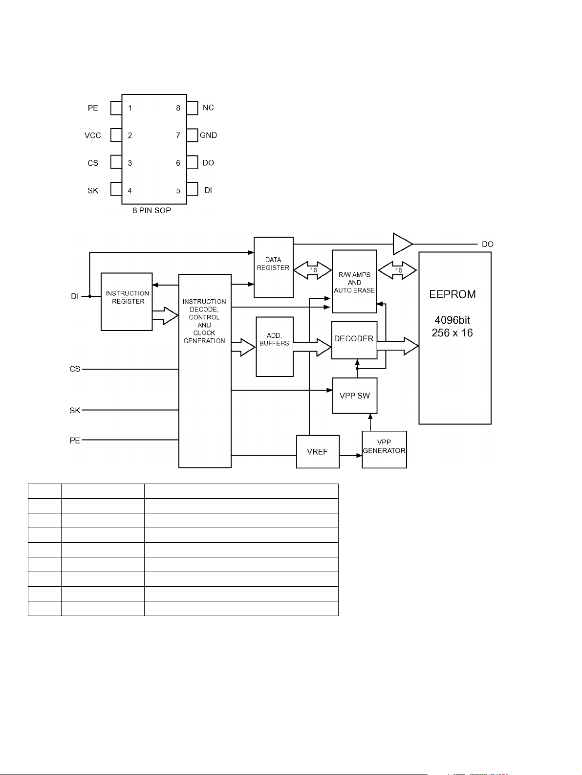
1.1 AK93C65AF-X (IC403) : EEPROM
• Pin layout
• Block diagram
SECTION 1
Description of major ICs
• Pin function
Pin no. Symbol Function
1 PE Program enable (With built-in pull-up resistor)
2 VCC Power supply
3 CS Chip selection
4 SK Cereal clock input
5 DI Cereal data input
6 DO Cereal data output
7 GND Ground
8 NC No connection
NOTE :
The pull-up resistor of the PE pin is about 2.5Mohm (VCC=5V)
2
Page 3
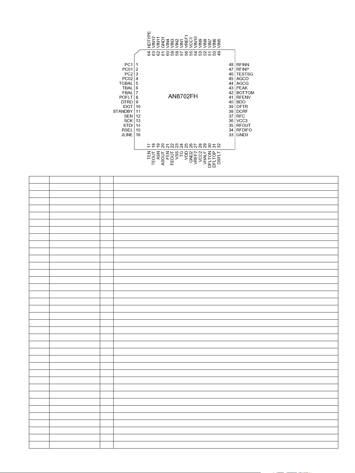
1.2 AN8702FH(IC101):Frontend processor
• Pin layout
• Pin function
Pin No. Symbol I/O Description
1 PC1 I Input for Laser current monitor
2 PC01 O Laser power control output for DVD
3 PC2 I Photo detector fo CD
4 PC02 O Laser power control output for CD
5 TGBAL I Tangential phase balance control terminal
6 TBAL I Tracking balance control terminal
7 FBAL I Focus balance control ter
8 POFLT O Track detection threshold level terminal
9 DTRD I Data slice part data read signal input terminal (For RAM)
10 IDGT I Data slice part address part gate signal input terminal (For RAM)
11 STANDBY I Standby mode control terminal
12 SEN I SEN(Serial data input terminal)
13 SCK I SCK(Serial data input terminal)
14 STDI I STDI(Serial data input terminal)
15 RSEL I DVD and CD selection
16 JLINE I J-line setting output (FEP)
17 TEN I Tracking error output amplifier reversing input terminal
18 TEOUT O Tracking error signal output terminal
19 ASN I Off set adjustment terminal for DRC
20 ASOUT O All added signal output terminal
21 FEN I Focus error output amplifier reversing input terminal
22 FEOUT O Focus error signal output terminal
23 VSS - Connect to GND
24 TG O Tangential phase error signal output terminal
25 VDD - Power supply terminal 3V
26 GND2 - Connect to GND
27 VREF2 O VREF2 voltage output terminal
28 VCC2 - Power supply terminal 5V
29 VHALF O VHALF voltage output terminal
30 DFLTON O Filter amplifier reversing output terminal
31 DFLTOP O Filter amplifier output terminal
32 DSFLT O Connected capacitor terminal for filter output
33 GND3 - Connect to GND
34 RFDIFO O RF operation output terminal
35 RFOUT O RF output terminal
36 VCC3 - Power supply terminal 5V
37 RFC I Filter for RF amplifier
XV-M50BK
3
Page 4
XV-M50BK
Pin No. Symbol I/O Description
38 DCRF O All addition amplifier capacitor terminal
39 OFTR O OFTR output teminalr
40 BDO O BDO output terminal
41 RFENV O RF envelope output terminal
42 BTTOM O Bottom envelope detection filter terminal
43 PEAK O Peak envelope detection filter terminal
44 AGCG O AGC amplifier gain control teminalr
45 AGCO O AGC amplifier level control terminal
46 TESTSG I TEST signal input terminal
47 RFINP I RF signal positive input terminal
48 RFINN I RF signal negative input terminal
49 VIN5 I RF input of external division into 4 terminal for CD
50 VIN6 I RF input of external division into 4 terminal for CD
51 VIN7 I RF input of external division into 4 terminal for CD
52 VIN8 I RF input of external division into 4 terminal for CD
53 VIN9 I RF input of external division into 2 terminal for DVD
54 VIN10 I RF input of external division into 2 terminal for DVD
55 VCC1 - Power supply terminal 5V
56 VREF1 O VREF1 voltage output terminal
57 VIN1 I External division into four (DVD/CD) RF input terminal1
58 VIN2 I External division into four (DVD/CD) RF input terminal2
59 VIN3 I External division into four (DVD/CD) RF input terminal3
60 VIN4 I External division into four (DVD/CD) RF input terminal4
61 GND1 - Connect to GND
62 VIN11 I 3 beem sub input terminal for CD
63 VIN12 I 3 beem sub input terminal for CD
64 HDTYPE I HD type switching
4
Page 5
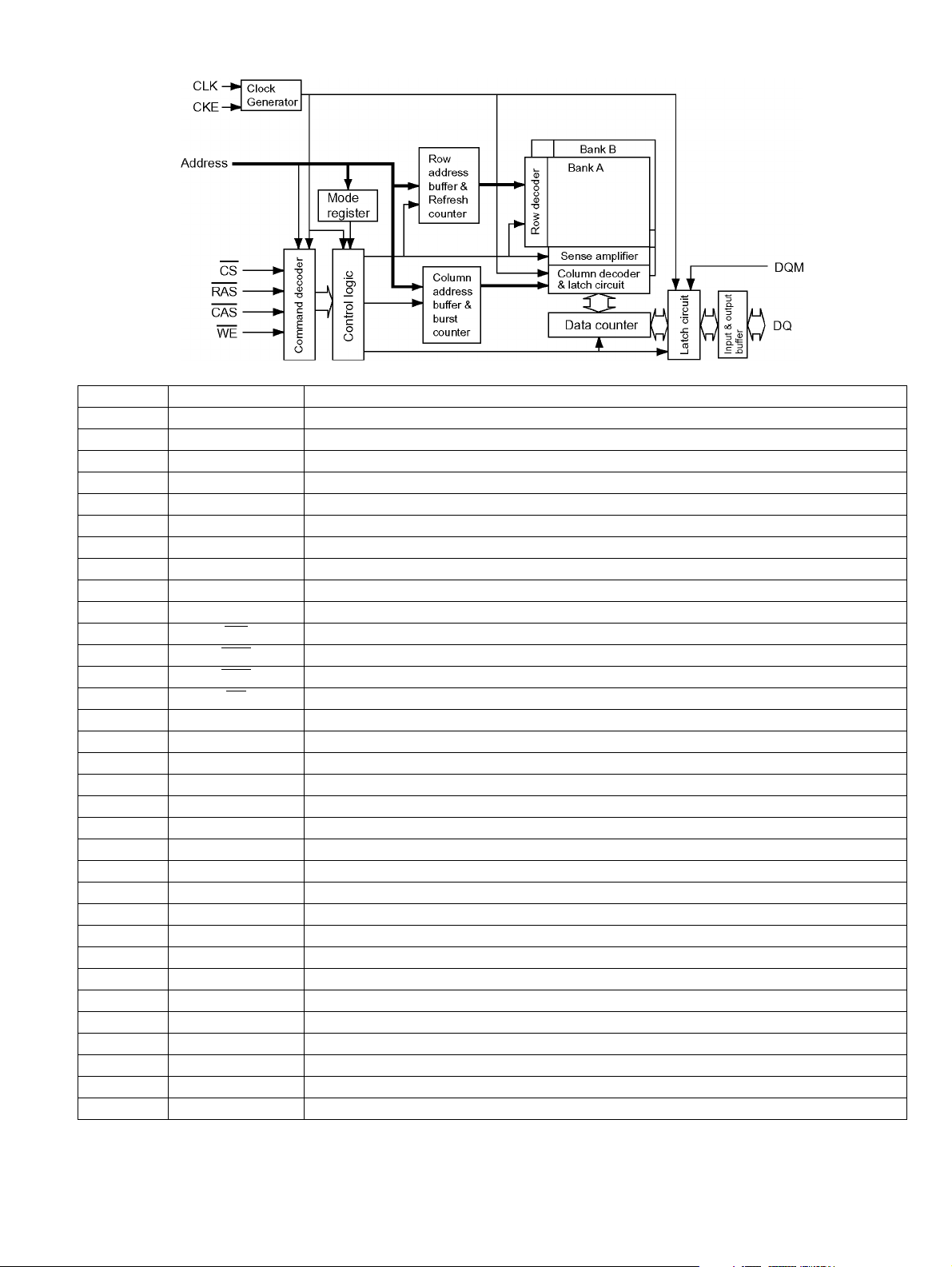
1.3 HY57V161610DTC8(IC504,IC505) : 16MB SDRAM
• Block diagram
• Pin function
Pin No. Symbol Description
1 VCC Power supply
2,3 DQ0,1 Data input/output
4 VSS Connect to GND
5,6 DQ2,3 Data input/output
7 VDD Power supply
8,9 DQ4,5 Data input/output
10 VSS Connect to GND
11,12 DQ6,7 Data input/output
13 VCC Power supply
14 LDQM Lower DQ mask enable
15
16
17
18
19,20 A11,10 Address inputs
21~24 A0~3 Address inputs
25 VCC Power supply
26 VSS Connect to GND
27~32 A4~9 Address inputs
33 NC Non connect
34 CKE Clock enable
35 CLK System clock input
36 UDQM Upper DQ mask enable
37 NC Non connect
38 VCC Power supply
39,40 DQ8,9 Data input/output
41 VSS Connect to GND
42,43 DQ10,11 Data input/output
44 VDD Power supply
45,46 DQ12,13 Data input/output
47 VSS Connect to GND
48,49 DQ14,15 Data input/output
50 VSS Connect to GND
WE
CAS
RAS
CS
Write enable
Column address strobe
Row address strobe
Chip enable
XV-M50BK
5
Page 6
XV-M50BK
1.4 M35500AFP(IC802) : FL Driver
• Pin layout
• Pin function
Pin No. Symbol I/O Description
1 VDD - Power supply terminal
2 XOUT O The short-circuit is made and the capacitor is connected with XIN on the outside
3 VSS - Connect to ground
4 XIN I The short-circuit is made and the capacitor is connected with XOUT on the outside
5 RESET I Reset input L:Reset
6~11 AIN5~0 I Key control signal input
12 CS I Chip select input L:The serial transfer is possible
13 SIN I Serial data input
14 SOUT O Serial data output
15 SCLK I Clock input of serial transfer
16,17 VEE - The voltage supplied to the pull down resistance is impressed
18~20 DISC3~1 IND O Indicator control signal output of disc indicator 1~3
21,22 NC - Not use
23~29 7G~1G O FL Grid control signal output
30~43 S14~S1 O FL Segment control signal output
44 VDD - Power supply terminal
6
Page 7
1.5 M56788FP-W (IC271) : Traverse mechanism driver
• Terminal Layout
XV-M50BK
• Block diagram
7
Page 8
XV-M50BK
1.6 MN101C49GGJ1(IC701): System controller
• Terminal layout
• Pinfunction
Pin No. Symbol I/O Function
1 GND - Connect to ground
2 NC - No connect
3 NC - No connect
4 NC - No connect
5 NTSEL I NTSC/PAL selection
6 POWER SW I Power switch detect terminal
7 SHUT1 - Connect to VDD
8 KEY1-5 - Connect to VDD
9 KEY6-10 - Connect to VDD
10 VREF+ I Reference voltage
11 VDD I Power supply
12 OSC2 O External terminal for connected oscirator
13 OSC1 I External terminal for connected oscirator
14 VSS - Connect to ground
15 XI - Connect to ground
16 XO - No connect
17 MMOD - Connect to ground
18 DADATA I/O Data bus for DAC
19 DACSO O Serial bus output for DAC
20 DACK I/O Clock for DAC
21 S2UDT O Communication between unit microcomputers DATA output
22 U2SDT I Communication between unit microcomputers DATA output
23 SCLK I/O Serial clock bus
24 BUSY I/O Busy bus
25 CPURST O Unit microcomputer reset
26 REQ I Commnication between unit microcomputers REQ
27 REMO I Remote control interrruption
28 - Non connect
29 - Non connect
30 - Connect to ground
31 - Connect to ground
32 - Connect to ground
33 RESET I DVD reset
34 - No connect
35 - No connect
36 VCD - No connect
37 OSDCK - No connect
38 NT - No connect
39 FS2 - No connect
8
Page 9
Pin No. Symbol I/O Function
40 CHREQ I Changer commnication REQUEST
41 CHST O Changer commnication STROBE
42 CHDATA O Changer commnication DATA I/O
43 - No connect
44 CHCK I Channel clock
45 FLDATAO O Serial data output
46 FLDATAI I Serial data input
47 FLCK O Clock output of serial transfer
48 FLCS O Chip select output
49 FLRST O Reset output
50 EEDO O Data output to EEPROM
51 EEDI I Data input from EEPROM
52 EECK O Clock signal output to EEPROM
53 EECS O Chip select output to EEPROM
54 VS1 O Fanction SW control
55 VS3 O Fanction SW control
56 DMUT1 - No connect
57 DMUT2 - No connect
58 PDB2 - No connect
59 PDB1 - No connect
60 DEMP2 - No connect
61 DEMP1 - No connect
62 DENA - No connect
63 KARAOKE O KARAOKE Mode switching terminal
64 POWER ON O Power on control output
65 VS2 - No connect
66 - No connect
67 - No connect
68 - No connect
69 - No connect
70 - No connect
71 - No connect
72 - No connect
73 - No connect
74 - No connect
75 - No connect
76 - No connect
77 AVCI I AV compulink signal input
78 AVCO O AV compulink signal output
79 RGB O RGB select control signal output
80 STDIND O Standby LED control signal output
81 - No connect
82 - No connect
83 - No connect
84 - No connect
85 - No connect
86 CS4 - No connect
87 MA - No connect
XV-M50BK
9
Page 10
XV-M50BK
Pin No. Symbol I/O Function
88 MB - No connect
89 M1M3 - No connect
90 MD - No connect
91 MC - No connect
92 GAIN2 - No connect
93 GAIN1 - No connect
94 HPMUT - No connect
95 DAVSS - No connect
96 LMUTE - No connect
97 CMUTE - No connect
98 SMUTE - No connect
99 MUTE O Muting control signal output
100 DAVDD - Power supply terminal
10
Page 11
1.7 MN102L62GGP (IC401) : Unit CPU
XV-M50BK
PinNo. Symbol I/O Function
1 WAIT I Micon wait signal input
2 RE O Read enable
3 SPMUTE O Spindle muting output to IC251
4 WEN O Write enable
5CS0-Not use
6 CS1 O Chip select for ODC
7 CS2 O Chip select for ZIVA
8 CS3 O Chip select for outer ROM
9 DRVMUTE O Driver mute
10 SPKICK - Non connect
11 LSIRST O LSI reset
12 WORD I Bus selection input
13 A0 O Address bus 0 for CPU
14 A1 O Address bus 1 for CPU
15 A2 O Address bus 2 for CPU
16 A3 O Address bus 3 for CPU
17 VDD - Power supply
18 SYSCLK - Non connect
19 VSS - Ground
20 XI - Not use (Connect to vss)
21 XO - Non connect
22 VDD - Power supply
23 OSCI I Clock signal input(13.5MHz)
24 OSCO O Clock signal output(13.5MHz)
25 MODE I CPU Mode selection input
26 A4 O Address bus 4 for CPU
27 A5 O Address bus 5 for CPU
28 A6 O Address bus 6 for CPU
29 A7 O Address bus 7 for CPU
30 A8 O Address bus 8 for CPU
31 A9 O Address bus 9 for CPU
32 A10 O Address bus 10 for CPU
33 A11 O Address bus 11 for CPU
34 VDD - Power supply
35 A12 O Address bus 12 for CPU
36 A13 O Address bus 13 for CPU
37 A14 O Address bus 14 for CPU
38 A15 O Address bus 15 for CPU
39 A16 O Address bus 16 for CPU
40 A17 O Address bus 17 for CPU
41 A18 O Address bus 18 for CPU
42 A19 O Address bus 19 for CPU
43 VSS - Ground
44 A20 O Address bus 20 for CPU
45 TXSEL O TX Select
46 HAGUP O Connect to pick-up
47 CD/DVD I CD/DVD Detect signal
48 ADPD O Power down control signal to IC511
49 HMFON O HFM Control output to IC102
50 TRVSW I Detection switch of traverse inside
51 FGIN I Focus gain input
52 TRS
53 ADSCEN O Servo DSC serial I/F chip select
PinNo. Symbol I/O Function
54 VDD - Power supply
55 FEPEN O Serial enable signal for FEP
56 SLEEP O Standby signal for FEP
57 BUSY I Communication busy
58 REQ O Communication request
59 CIRCEN O CIRC serial I/F chip select
60 HSSEEK
61 VSS - Ground
62 EPCS O EEPROM chip select
63 EPSK O EEPROM clock
64 EPDI I EEPROM data input
65 EPDO O EEPROM data output
66 VDD - Power supply
67 SCLKO O Communication clock
68 S2UDT I Communication input data
69 U2SDT O Communication output data
70 CPSCK O Clock for ADSC serial
71 SDIN I ADSC serial data input
72 SDOUT O ADSC serial data output
73 - I Not use (Pull up)
74 - I Not use (Pull up)
75 NMI I NMI Terminal
76 ADSCIRQ I Interrupt input of ADSC
77 ODCIRQ I Interrupt input of ODC
78 DECIRQ I Interrupt input of ZIVA
79 WAKEUP - Connect to ground
80 ODCIRQ2 I Interruption of system control
81 ADSEP I Address data selection input
82 RST I Reset input
83 VDD - Power supply
84 TEST1 I Test signal 1 input
85 TEST2 I Test signal 2 input
86 TEST3 I Test signal 3 input
87 TEST4 I Test signal 4 input
88 TEST5 I Test signal 5 input
89 TEST6 I Test signal 6 input
90 TEST7 I Test signal 7 input
91 TEST8 I Test signal 8 input
92 VSS - Ground
93 D0 I/O Data bus 0 of CPU
94 D1 I/O Data bus 1 of CPU
95 D2 I/O Data bus 2 of CPU
96 D3 I/O Data bus 3 of CPU
97 D4 I/O Data bus 4 of CPU
98 D5 I/O Data bus 5 of CPU
99 D6 I/O Data bus 6 of CPU
100 D7 I/O Data bus 7 of CPU
11
Page 12

XV-M50BK
1.8 MN103S13BDA(IC301):Optical disc controller
• Pin layout
• Block diagram
12
Page 13

• Pin function
PinNo. Symbol I/O Description
1 HDD15 I/O ATAPI Data
2 HDD0 I/O ATAPI Data
3 HDD14 I/O ATAPI Data
4 VDD - Power supply 3V
5 HDD1 I/O ATAPI Data
6 HDD13 I/O ATAPI Data
7 HDD2 I/O ATAPI Data
8 VSS - Connect to GND
9 HDD12 I/O ATAPI Data
10 VDD - Power supply 2.7V
11 HDD3 I/O ATAPI Data
12 HDD11 I/O ATAPI Data
13 HDD4 I/O ATAPI Data
14 HDD10 I/O ATAPI Data
15 VDD - Power supply 3V
16 HDD5 I/O ATAPI Data
17 HDD9 I/O ATAPI Data
18 VSS - Connect to GND
19 HDD6 I/O ATAPI Data
20 HDD8 I/O ATAPI Data
21 HDD7 I/O ATAPI Data
22 VDDH
23 NRESET I ATAPI Reset input
24 MASTER I/O ATAPI Master/slave select
25 NINT0 O Interruption of system control 0
26 NINT1 O Interruption of system control 1
27 WAITDOC O Wait control of system control
28 NMRST O Reset of system control (Connect to TP302)
29 DASPST I Setting of initial value of DASP signal
30 VDD - Power supply 3V
31 OSCO2 O Non connect
32 OSCI2 I Non connect
33 UATASEL I Connect to VSS
34 VSS - Connect to GND
35 PVSSDRAM Connect to VSS
36 PVDDDRAM Connect to VDD(2.7V)
37 CPUADR17 I System control address
38 CPUADR16 I System control address
39 VSS - Connect to GND
40 CPUADR15 I System control address
41 CPUADR14 I System control address
42 CPUADR13 I System control address
43 CPUADR12 I System control address
44 VDD - Power supply 2.7V
45 CPUADR11 I System control address
46 CPUADR10 I System control address
47 CPUADR9 I System control address
48 CPUADR8 I System control address
XV-M50BK
13
Page 14

XV-M50BK
PinNo. Symbol I/O Description
49 CPUADR7 I System control address
50 CPUADR6 I System control address
51 CPUADR5 I System control address
52 CPUADR4 I System control address
53 CPUADR3 I System control address
54 CPUADR2 I System control address
55 CPUADR1 I System control address
56 VSS - Connect to GND
57 CPUADR0 I System control address
58 NCS I System control chip select
59 NWR I Writing system control
60 NRD I Reading system control
61 VDD - Power supply 3V
62 CPUDT7 I/O System control data
63 CPUDT6 I/O System control data
64 PVPPDRAM O Connect to VSS
65 PTESTDRAM I Connect to VSS
66 PVDDDRAM Connect to VDD(2.7V)
67 PVSSDRAM Connect to VSS
68 CPUDT5 I/O System control data
69 CPUDT4 I/O System control data
70 CPUDT3 I/O System control data
71 VSS - Connect to GND
72 CPUDT2 I/O System control data
73 CPUDT1 I/O System control data
74 CPUDT0 I/O System control data
75 CLKOUT1 O Clock signal output (16.9/11.2/8.45MHz)
76 VDD - Power supply 3V
77 TEHLD O Mirror gate (Connect to TP141)
78 DTRD O Data frequency control switch (Connect to TP304)
79 IDGT O CAPA switch
80 BDO I RF Dropout/BCA data
81 CPDET2 I Outer capacity detection
82 CPDET1 I Inner capacity detection
83 VSS - Connect to GND
84 MMOD I Connect to VSS
85 NRST I System reset
86 VDD - Power supply 3V
87 CLKOUT2 O Clock 16.9MHz
88 SBCK/PLLOK O Flame mark detection
89 IDOHOLD O ID gate for tracking holding
90 JMPINH O Jump prohibition
91 LG O Land/group switch
92 NTRON I Tracking ON
93 DACDATA O Serial data output (Connect to TP148)
94 DACLRCK O Identification signal of L and R (Connect to TP149)
95 DACCLK I Clock for serial data output
96 IPFLAG I Input of IP flag
14
Page 15

PinNo. Symbol I/O Description
97 BLKCK I Sub code/block/input clock
98 LRCK I Identification signal of L and R (Connect to VSS)
99 VSS - Connect to GND
100 OSCI1 I Oscillation input terminal 16.9MHz
101 OSCO1 O Oscillation output terminal 16.9MHz
102 VDD - Power supply 3V
103 PVSS - Connect to GND
104 PVDD - Power supply 3V
105 P1 I/O Terminal master polarity switch input
106 P0 I/O CIRC-RAM,OVER/UNDER Interruption
107 VSS - Connect to GND
108 SBCK O Clock output for sub code,serial input
109 SUBC I Sub code,serial input
110 NCLDCK I Sub code,flame clock input
111 CHCK40 I Clock is read to D
112 DAT3 I AT3~0 (Output of division frequency from ADSC)
113 DAT2 I Data is read from disc (Going side by side output from ADSC)
114 DAT1 I Data is read from disc (Going side by side output from ADSC)
115 DAT0 I Data is read from disc (Going side by side output from ADSC)
116 VDD - Data is read from disc (Going side by side output from ADSC)
117 SCLOCK I/O Power supply 3V
118 SDATA I/O Debug serial clock (270 ohm pull up)
119 MONI3 O Debug serial data (270 ohm pull up)
120 MONI2 O Internal good title monitor (Connect to TP150)
121 MONI1 O Internal good title monitor (Connect to TP151)
122 MONI0 O Internal good title monitor (Connect to TP152)
123 VSS - Internal good title monitor (Connect to TP153)
124 NEJECT I Connect to GNDEject detection
125 VDD - Power supply 2.7V
126 NTRYCL I Non connect (Tray close detection)
127 NDASP I/O ATAPI drive active / slave connect I/O
128 NCS3FX I Non connect (ATAPI host chip select)
129 NCS1FX I Non connect (ATAPI host chip select)
130 VDD - Power supply 3V
131 DA2 I/O ATAPI host address
132 DA0 I/O Non connect (ATAPI host address)
133 NPDIAG I/O ATAPI Slave master diagnosis input
134 VSS - Connect to GND
135 DA1 I/O Non connect (ATAPI host address)
136 NIOCS16 O Output of selection of width of ATAPI host data bus
137 INTRQ O ATAPI Host interruption output
138 VDD - Power supply 3V
139 NDMACK I Non connect (ATAPI Host DMA characteristic)
140 IORDY O ATAPI Host ready output (Connect to TP157)
141 NIORD I Non connect (ATAPI host read)
142 VSS - Connect to GND
143 NIOWR I/O ATAPI Host writeAT
144 DMARQ O API Host DMA request (Connect to TP159)
XV-M50BK
15
Page 16

XV-M50BK
1.9 MN35505-X (IC703) : DAC
• Terminal layout
• Pin function
Pin No. Symbol I/O Description
1 M5 I Control signal for DAC
2 DIN I Digital data input
3 LRCK I L and R clock for DAC
4 BCK I Bit clock for DAC
5 M3 I Control signal for DAC
6 DVDD2 - Power supply terminal
7 CKO - Non connect
8 DVSS2 - Connect to ground
9 M2 I Control signal for DAC
10 M1 I Control signal for DAC
11 OUT1C O Analog output 1
12 AVDD1 - Power supply terminal
13 OUT1D O Analog output 1
14 AVSS1 - Connect to ground
15 AVSS2 - Connect to ground
16 OUT2D O Analog output 2
17 AVDD2 - Power supply terminal
18 OUT2C O Analog output 2
19 M9 I Control signal for DAC
20 DVSS1 - Connect to ground
21 XOUT - Non connect
22 XIN - Non connect
23 VCOF I VCO Frequency
24 DVDD1 - Power supply D+5V
25 M7 - Connect to ground
26 M8 - Connect to ground
27 M4 I Control signal for DAC
28 M6 I Clock for control signal
16
Page 17

1.10 MN67706ZY (IC201) : Auto digital servo controller
• Terminal layout
XV-M50BK
• Pin functions
Pin No Symbol I/O Function
1 AS(AD2) I AS :Full adder signal(FEP)
2 TE(AD1) I Phase difference/3 beam tracking error(FEP)
3 FE(AD0) I Focus error(FEP)
4 AVDD - Apply 3.3V(For analog circuit)
5 FODRV(DA1) O Focus drive(DRVIC)
6 TRDRV(DA0) O Tracking drive(DRVIC)
7 AVSS - Ground(For analog circuit)
8 ARF I Equivalence RF+(FEP)
9 NARF I Equivalence RF-(FEP)
10 IREF1 I Reference current1(For DBAL)
11 IREF2 I Reference current2(For DBAL)
12 DSLF1 I/O Connect to capacitor1 for DSL
13 DSLF2 I/O Connect to capacitor2 for DSL
14 AVDD - Apply 3.3V(For analog circuit)
15 VHALF I Reference voltage 1.65+-0.1V(FEP)
16 PLPG - Not use(PLL phase gain setting resistor terminal)
17 PLFG - Not use(PLL frequency gain setting resistor terminal)
18 VREFH I Reference voltage 2.2V+-0.1V(FEP)
19 RVI I/O Connect to resistor for VREFH reference current source
20 AVSS - Ground(For analog circuit)
21 PLFLT1 O Connect to capacitor1 for PLL
22 PLFLT2 O Connect to capacitor2 for PLL
23 JITOUT I/O Output for jitter signal monitor
17
Page 18

XV-M50BK
Pin No Symbol I/O Function
24 RFDIF I Not use
25 CSLFL1 I/O Pull-up to VHALF
26 VFOSHORT O VFO short output
27 AVDD - Apply 3.3V(For analog circuit)
28 HPFIN I Pull-up to VHALF
29 HPFOUT O Connect to TP208
30 AVSS - Ground(For analog circuit)
31 LPFIN I Pull-up to VHALF
32 LPFOUT O Not use
33 CMPIN I Connect to TP210
34 TRCRS I Input signal for track cross formation
35 VCOF I/O JFVCO control voltage
36 DBALO O DSL balance adjust output
37 JLINE O J-line setting output(FEP)
38 AVDD - Apply 3.3V(For analog circuit)
39 LOUT O Connect to TP203 (Analog audio left output)
40 ROUT O Connect to TP204 (Analog audio right output)
41 AVSS - Ground(For analog circuit)
42 TGBAL O Tangential balance adjust(FEP)
43 TBAL O Tracking balance adjust(FEP)
44 FBAL O Focus balance adjust(FEP)
45 33VSS - Ground(For I/O)
46 33VDD - Apply 3.3V(For I/O)
47 OFTR I Off track signal
48 SYSCLK I 16.9344MHz system clock input(ODC)
49 BDO I Drop out(FEP)
50 TSTSG O Calibration signal(FEP)
51 TRSDRV O Traverse drive(DRVIC)
52 SPDRV O Spindle drive output(DRVIC)
53 FG I FG signal input (Spindle motor driver)
54 TILTP O Connect to TP205
55 TILT O Connect to TP206
56 TILTN O Connect to TP207
57 25VSS - Ground(For internal core)
58 25VDD - Apply 2.5V(For internal core)
59 DTRD I Data read control signal(ODC)
60 IDGT/TEMUTE I Pull-down to Ground
61 LRCK/CPDET2 O LR channel data strobe(ODC)/
62 BLKCK/CPDET1 O CD sub code synchronous signal(ODC)/
63 SBCK/PLLOK I CD sub code data shift clock(ODC)/PLL pull-in OK signal input
64 IDHOLD I Pull-down to Ground
65 DACLRCK/JMPINH I 1bit DAC-LR channel data strobe(ODC)/
66 DACDATA/LG I CD 1bit DAC channel data(ODC)
67 NTRON O L :Tracking ON(ODC)
68 DACCLK O 1bit DAC channel data shift clock(ODC)
69 IPFLAG O CIRC error flag(ODC)
70 SUBC O CD sub code(ODC)
71 NCLDCK/JUMP O CD sub code data frame clock(ODC)/DVD JUMP signal(ODC)
18
Page 19

Pin No Symbol I/O Function
72 MINTEST I Pull-down to Ground(For MINTEST)
73 TEST I Pull-down to Ground(For TEST)
74 33VSS - Ground(For I/O)
75 33VDD - Apply 3.3V(For I/O)
76 CHCK40 O Clock for SRDATA(ODC)
77 DAT3 O SRDATA3(ODC)
78 DAT2 O SRDATA2(ODC)
79 DAT1 O SRDATA1(ODC)
80 DAT0 O SRDATA0(ODC)
81 33VSS - Ground(For I/O)
82 33VDD - Apply 3.3V(For I/O)
83 TX O Digital audio interface
84 XRESET I Reset input (System control)
85 ENS I Servo DSC serial I/F chip select (System control)
86 ENC I CIRC serial I/F chip select (System control)
87 CPUIRQ O Interrupt request (System control)
88 CPUCLK I Syscon serial I/F clock (System control)
89 CPUDTIN I Syscon serial I/F data input (System control)
90 CPUDTOUT O Syscon serial I/F data output (System control)
91 MONA O Connect to TP226 (Monitor terminal A)
92 MONB O Connect to TP225 (Monitor terminal A)
93 MONC O Connect to TP224 (Monitor terminal A)
94 NC O Connect to TP211
95 25VSS - Ground(For internal core)
96 25VDD - Apply 2.5V(For internal core)
97 LDCUR(AD6) I Laser current control terminal
98 TDOFS(AD5) I Connect to TP215
99 TG(AD4) I Tangential phase difference(FEP)
100 RFENV(AD3) I RF envelope input(FEP)
XV-M50BK
19
Page 20

XV-M50BK
1.11 MR27V1602EN8MAX (IC402) :P2 ROM of 1,048,576word x 16 bit / 2,097,152 word x 8 bit
• Pin layout
• Block diagram
• Pin functions
Symbol Function
A0 - A20 Address Input
D0 - D14 Data Output
CE Chip Enable
OE Output Enable
BYTE Mode Switch
Vcc Power Supply
Vss GND
WE Write enable
WP Connect to ground
20
Page 21

1.12 TA8409S (IC802,IC803) : Motor driver
• Pin layout
• Pin function
INPUT OUTPUT MODE
IN1 IN2 OUT 1 OUT 2 MOTOR
0 0 Infinity Infinity STOP
1 0 H L CW/CCW
01 LH CCW/CW
1 1 L L BRAKE
• Pin function
Pin No. Symbol Description
1 IN2 Input terminal
2 Vcc Power supply terminal for logic
3 OUT2 Output terminal
4 NC Non connect
5 GND Connect to ground
6 Vs Power supply terminal for motor driver
7 OUT1 Output terminal
8 Vref Reference voltage terminal for control circuit
9 IN1 Input terminal
XV-M50BK
21
Page 22

XV-M50BK
1.13 TC74VHC00FT-X (IC503) : Write timing control
• Terminal layout / Block diagram
1.14 TC74VHC125FT-X (IC411) : Buffer
• Terminal layout / Block diagram
• Truth table
ABY
LLH
LHH
HLH
HHL
• Truth table
INPUTS OUTPUTS
G
HX Z
LL L
LH H
AY
X : Don’t care
Y : High impedance
1.15 TC7WT125FU-X(IC412) : Dual bus buffer
• Pin layout • Truth table
INPUTS OUTPUTS
G
HX Z
LL L
LH H
X : Don’t care
Y : High impedance
AY
22
Page 23

1.16 UPD65612GB-208(IC801):Changer control micon
• Terminal layout
• Pin function
Pin No. Symbol I/O Function
1 NC - Non connect
2 NC - Non connect
3 MSPOSI - Non connect
4 OS1I I Oscillation input terminal
5 OS1O O Oscillation output terminal
6 OS2I I Oscillation input terminal
7 OS2O O Oscillation output terminal
8 NC - Non connect
9 C12IN I Connect to C12 OUT terminal
10 C12OUT O Connect to C12 IN terminal
11 RESET I Reset signal input
12 REQB O Mecha.data.request output
13 DATA I/O Control.status.data.I/O
14 STCH I Strobe signal input
15 CKS I Clock signal input
16 SELECT - Connect to ground
17 GND - Connect to ground
18 CK - Connect to ground
19 1MSW I Switch input signal to TRAY1
20 2MSW I Switch input signal to TRAY2
21 3MSW I Switch input signal to TRAY3
22 3SSW I Switch input signal to TRAY3
XV-M50BK
Pin No. Symbol I/O Function
23 2SSW I Switch input signal to TRAY2
24 1SSW I Switch input signal to TRAY1
25 NC - Non connect
26 CAM0 I Switch input signal for LCAM
27 CAM1 I Switch input signal for LCAM
28 CAM2 I Switch input signal for LCAM
29 CAM3 I Switch input signal for LCAM
30 CAM4 I Switch input signal for RCAM
31 CAM5 I Switch input signal for RCAM
32 CAM6 I Switch input signal for RCAM
33 CAM7 I Switch input signal for RCAM
34 FIT O Connect to C50
35 C50 I Connect to FIT
36 LMUP O Motor control signal for L
37 LMDWN O Motor control signal for L
38 C25 - Non connect
39 VDD - Power supply
40 C100 - Non connect
41 RMUP O Motor control signal for R
42 RMDWN O Motor control signal for R
43 NC - Non connect
44 NC - Non connect
23
Page 24

XV-M50BK
1.17 ZIVA-4.1-PB0(IC501) : Back end - Digital decoder
• Terminal layout
• Pin function
Pin No. Symbol I/O Description
1RD
2R/W
3 VDD_3.3 - Power supply terminal 3.3V
4WAIT
5 RESET
6 VSS - Connect to ground
7 VDD_3.3 - Power supply terminal 3.3V
8INT
9 NC - Non connect
10 NC - Non connect
11 NC - Non connect
12 NC - Non connect
13 VDD_2.5 - Power supply terminal 2.5V
14 VSS - Connect to ground
15 NC - Non connect
16 NC - Non connect
17 NC - Non connect
18 NC - Non connect
19 VSS - Connect to ground
20 VDD_3.3 - Power supply 3.3V
21 VDATA0 O Video data bus output. Byte serial CbYCrY data synchronous with VCLK.
22 VDATA1 O Video data bus output. Byte serial CbYCrY data synchronous with VCLK.
23 VDATA2 O Video data bus output. Byte serial CbYCrY data synchronous with VCLK.
24 VDATA3 O Video data bus output. Byte serial CbYCrY data synchronous with VCLK.
25 VDATA4 O Video data bus output. Byte serial CbYCrY data synchronous with VCLK.
26 VDATA5 O Video data bus output. Byte serial CbYCrY data synchronous with VCLK.
27 VDATA6 O Video data bus output. Byte serial CbYCrY data synchronous with VCLK.
28 VDATA7 O Video data bus output. Byte serial CbYCrY data synchronous with VCLK.
29 VSYNC
30 HSYNC
31 VSS - Connect to ground
32 VDD_3.3 - Power supply terminal 3.3V
33 NC - Non connect
34 NC - Non connect
35 NC - Non connect
36 VDD_2.5 - Power supply terminal 2.5V
37 VSS - Connect to ground
I Read strobe input
I Read/write strobe input
O Transfer not complete / data acknowledge.
Active LOW to indicate host initiated transfer is complete.
I Active LOW : reset signal input
O Host interrupt signal output
I/O Vertical sync. Bi-directional the decoder output the top border of a new field on the first HSYNC
after the falling edge of VSYNC.
I/O Horizontal sync. The decoder begins outputting pixel data for a new horizontal line after the
falling (active) edge of HSYNC.
24
Page 25

Pin No. Symbol I/O Description
38 NC - Non connect
39 NC - Non connect
40 NC - Non connect
41 NC - Non connect
42 NC - Non connect
43 PIO0 I/O Programmable I/O terminal
44 VSS - Connect to ground
45 VDD_3.3 - Power supply terminal 3.3V
46 PIO1 I/O Programmable I/O terminal
47 PIO2 I/O Programmable I/O terminal
48 PIO3 I/O Programmable I/O terminal
49 PIO4 I/O Programmable I/O terminal
50 PIO5 I/O Programmable I/O terminal
51 PIO6 I/O Programmable I/O terminal
52 PIO7 I/O Programmable I/O terminal
53 MDATA0 I/O SDRAM data
54 MDATA1 I/O SDRAM data
55 VDD_3.3 - Power supply terminal 3.3V
56 VSS - Connect to ground
57 MDATA2 I/O SDRAM data
58 MDATA3 I/O SDRAM data
59 MDATA4 I/O SDRAM data
60 MDATA5 I/O SDRAM data
61 MDATA6 I/O SDRAM data
62 MDATA7 I/O SDRAM data
63 MDATA15 I/O SDRAM data
64 VDD_3.3 - Power supply terminal 3.3V
65 VSS - Connect to ground
66 MDATA14 I/O SDRAM data
67 VDD_2.5 - Power supply terminal 2.5
68 VSS - Connect to ground
69 MDATA13 I/O SDRAM data
70 MDATA12 I/O SDRAM data
71 MDATA11 I/O SDRAM data
72 MDATA10 I/O SDRAM data
73 MDATA9 I/O SDRAM data
74 VDD_3.3 - Power supply terminal 3.3V
75 VSS - Connect to ground
76 MDATA8 I/O SDRAM data
77 LDQM O SDRAM Lower or upper mask
78 SD-CLK O SDRAM Clock
79 CLKSEL I Selects SYSCLK or VCLK as clock source. Normal operation is to tie HIGH.
80 MADDR9 O SDRAM address
81 MADDR8 O SDRAM address
82 VDD_3.3 - Power supply terminal 3.3V
83 VSS - Connect to ground
84 MADDR7 O SDRAM address
85 MADDR6 O SDRAM address
XV-M50BK
25
Page 26

XV-M50BK
Pin No. Symbol I/O Description
86 MADDR5 O SDRAM address
87 VDD_2.5 - Power supply terminal 2.5V
88 VSS - Connect to ground
89 MADDR4 O SDRAM address
90 MWE
91 SD-CAS
92 VDD_3.3 - Power supply terminal 3.3V
93 VSS - Connect to ground
94 SD-RAS
95 SD-CS0
96 SD-CS1
97 SD-BS
98 MADDR10 O SDRAM address
99 MADDR0 O SDRAM address
100 VDD_3.3 - Power supply terminal 3.3V
101 VSS - Connect to ground
102 MADDR1 O SDRAM address
103 MADDR2 O SDRAM address
104 MADDR3 O SDRAM address
105 RESERVED I Tie to VSS or VDD_3.3 as specified in table 1
106 NC - Non connect
107 NC - Non connect
108 RESERVED I Tie to VSS or VDD_3.3 as specified in table 1
109 NC - Non connect
110 RESERVED I Tie to VSS or VDD_3.3 as specified in table 1
111 RESERVED I Tie to VSS or VDD_3.3 as specified in table 1
112 RESERVED I Tie to VSS or VDD_3.3 as specified in table 1
113 DAI-LRCK I PCM left/right clock
114 DAI-BCK I PCM input bit clock
115 VDD_3.3 - Power supply 3.3V
116 VSS - Connect to ground
117 DAI-DATA I PCM data input
118 DA-DATA3 O PCM data output. Eight channels. Serial audio samples relative to DA_BCK and DA_LRCK
119 DA-DATA2 O PCM data output. Eight channels. Serial audio samples relative to DA_BCK and DA_LRCK
120 DA-DATA1 O PCM data output. Eight channels. Serial audio samples relative to DA_BCK and DA_LRCK
121 DA-DATA0 O PCM data output. Eight channels. Serial audio samples relative to DA_BCK and DA_LRCK
122 DA-LRCK O PCM left clock. Identifies the channel for each sample
123 VDD_3.3 - Power supply terminal 3.3V
124 VSS - Connect to ground
125 DA-XCK I/O Audio external frequency clock input or output
126 DA-BCK O PCM bit clock output
127 DA-IEC O PCM data out in IEC-958 format or compressed data out in IEC-1937 format
128 VDD_2.5 - Power supply terminal 2.5V
129 VSS - Connect to ground
130 NC - Non connect
131 VSS_DAC - Connect to ground for analog video DAC
132 VSS_VIDEO - Connect to ground for analog video
133 CVBS O DAC video output format : CVBS. Macrovision encoded
/MADDR11 O Active LOW SDRAM chip select 1 or use as MADDR11 for larger SDRAM
O SDRAM write enable
O Active LOW SDRAM column address
O Active LOW SDRAM row address
O Active LOW SDRAM chip select 0
O SDRAM bank select
26
Page 27

Pin No. Symbol I/O Description
134 VDD_DAC - Power supply terminal for analog video DAC
135 VDD_VIDEO - Power supply terminal for analog video
136 NC - Non connect
137 VSS_DAC - Connect to ground for analog video DAC
138 VSS_VIDEO - Connect to ground for analog video
139 CVBS/G/Y O DAC video output format. Macrovision encoded
140 VDD_DAC - Power supply terminal for analog video DAC
141 VDD_VIDEO - Power supply terminal for analog video
142 NC - Non connect
143 VSS_DAC - Connect to ground for analog video DAC
144 VSS_VIDEO - Connect to ground for analog video
145 Y/B/U O DAC video output format. Macrovision encoded
146 VDD_DAC - Power supply terminal for analog video DAC
147 VDD_VIDEO - Power supply terminal for analog video
148 NC - Non connect
149 VSS_DAC - Connect to ground for analog video DAC
150 VSS_VIDEO - Connect to ground for analog video
151 C/R/V O DAC video output format. Macrovision encoded
152 VDD_DAC - Power supply terminal for analog video DAC
153 VDD_VIDEO - Power supply terminal for analog video
154 VSS_RREF - Connect to ground for analog video
155 RREF O Reference resistor. Connecting to pin 154
156 VDD_RREF - Power supply terminal for analog video 3.3V
157 A_VSS - Power supply terminal for analog PLL 3.3V
158 SYSCLK I Optical system clock. Tie to A_VDD through a 1K ohm resistor
159 VCLK I System clock input
160 A_VDD - Power supply terminal for analog PLL 3.3V
161 DVD-DATA0/CD-
DATA
162 DVD-DATA1/CD-
LRCK
163 DVD-DATA2/CD-
BCK
164 DVD-DATA3/CD-
C2PO
165 DVD-DATA4/
CDGSDATA
166 VSS - Connect to ground
167 VDD_3.3 - Power supply terminal 3.3V
168 DVD-DATA5/CDG-
VFSY
169 DVD-DATA6/CDG-
SOS1
170 DVD-DATA7/CDG-
SCLK
171 VDACK I In synchronous mode bit stream data acknowledge. Asserted when DVD data is valid. Polarity
172 VREQUEST O Bit stream request
173 VSTROBE I Bit stream strobe
174 ERROR I Error in input data
I Serial CD data. This pin is shared with DVD compressed data DVD-DATA0
I Programmable polarity 16-bit word synchronization to the decoder.
This pin is shared with DVD compressed data DVD-DATA1
I CD bit clock. Decoder accept multiple BCK rates. This pin is shared with DVD compressed
DVD-DATA2
I Asserted HIGH indicates a corrupted byte. This pin is shared with DVD compressed data DVD-
DATA3
I DVD parallel compressed data from DVD DSP. or CD-G data indicating serial sub code data
input
I DVD parallel compressed data from DVD DSP. or CD-G frame sync indicating frame-start or
composite synchronization input.
I DVD parallel compressed data from DVD DSP. or CD-G block sync indicating block-start syn-
chronization input
I DVD parallel compressed data from DVD DSP. or CD-G clock indicating sub code data clock
input or output
is programmable
XV-M50BK
27
Page 28

XV-M50BK
Pin No. Symbol I/O Description
175 VDD_3.3 - Power supply terminal 3.3V
176 RESERVED I Tie to VSS or VDD_3.3 as specified in table 1
177 VDD_3.3 - Power supply terminal 3.3V
178 VSS - Connect to ground
179 NC - Non connect
180 RESERVED I Tie to VSS or VDD_3.3 as specified in table 1
181 NC - Non connect
182 HADDR0 I Host address bus. 3-bit address bus selects one of eight host interface registers
183 HADDR1 I Host address bus. 3-bit address bus selects one of eight host interface registers
184 HADDR2 I Host address bus. 3-bit address bus selects one of eight host interface registers
185 RESERVED I Tie to VSS or VDD_3.3 as specified in table 1
186 RESERVED I Tie to VSS or VDD_3.3 as specified in table 1
187 RESERVED I Tie to VSS or VDD_3.3 as specified in table 1
188 VSS - Connect to ground
189 VDD_2.5 - Power supply terminal 2.5V
190 RESERVED I Tie to VSS or VDD_3.3 as specified in table 1
191 VSS - Connect to ground
192 VDD_3.3 - Power supply terminal 3.3V
193 RESERVED I Tie to VSS or VDD_3.3 as specified in table 1
194 RESERVED I Tie to VSS or VDD_3.3 as specified in table 1
195 RESERVED I Tie to VSS or VDD_3.3 as specified in table 1
196 RESERVED I Tie to VSS or VDD_3.3 as specified in table 1
197 HDATA7 I/O The 8-bit bi-derectional host data through which the host writes data to the decoder code.
198 VSS - Connect to ground
199 HDATA6 I/O The 8-bit bi-derectional host data through which the host writes data to the decoder code.
200 HDATA5 I/O The 8-bit bi-derectional host data through which the host writes data to the decoder code.
201 HDATA4 I/O The 8-bit bi-derectional host data through which the host writes data to the decoder code.
202 HDATA3 I/O The 8-bit bi-derectional host data through which the host writes data to the decoder code.
203 HDATA2 I/O The 8-bit bi-derectional host data through which the host writes data to the decoder code.
204 VDD_3.3 - Power supply terminal 3.3V
205 VSS - Connect to ground
206 HDATA1 I/O The 8-bit bi-derectional host data through which the host writes data to the decoder code.
207 HDATA0 I/O The 8-bit bi-derectional host data through which the host writes data to the decoder code.
208 CS
I Host chip select input
28
Page 29

2.1 General view
J691 (Only Europe)
AUDIO
RGB
G
C/R
LEA10018-A4
Video board
S-VIDEO
OUT
COMPOSITE
VIDEO OUT
J602 (For Asia) , J692 (For Europe)
Y/COMPOSITE
Y
B
C
Q631
Block diagrams
COMPONENT
VIDEO OUT
J601 (Only Asia)
Y
Pb(Cb)
Q611
Q621
Q601
SECTION 2
Pr(Cr)
CN601
CN503
J701
LPF
IC741
AUDIO OUT
R
2/2
1/2
L
2/2
1/2
IC751
LPF
J703
OPTICAL DIGITAL
OUT
COAXIAL DIGITAL
OUT
J704
J702
AV COMPULINK
Q709
XV-M50BK
CN961
LEA10018-A1
Power supply board
CN981
CN501
MIC OUT
M9V
D2.5V
/D3V
/D5V
IC511
IC101
Front End
*This block is only US,UY,UW,UG,A
AD Converter
IC401
UNIT CPU
Processor
IC301
IC201
IC501AVDecorder
Optical
Disc
Digital
Servo
Controller
Controller
System control board
CN502
IC703
CN701
LEA10018-A3
DAC
CN702
CN801
controller section
Changer mechanism
LVA10018-A2
FL indicator board
FW851
CN703
CN801
FL Display
IC701
System
Microprosessor
IC802
FL Driver
FW872
IC801
Remote
controller
S821-S826
S831-S835
Operation switch
FW803
S801
Power switch
LVA10228-A1
Traverse mechanism control board
LVA10132
Connection board
CN101
CN10
CN12
DVD
PICK-UP
Tracking
Focus
PHOTO
IC271
FM
SM
IC851
J851
MIC. AMP.
1/2
MIC. 1 IN
LVA10018-A6
2/2
MIC. 2 IN
J852
IC871
MIC. MIX. AMP.
MIC. 1 VR
FW851
LVA10018-A7
MIC. 2 VR
*This block is only US,UY,UW,UG,A
29
Page 30

XV-M50BK
2.2 DVD Servo control section (SHEET 1,2)
SYSCLK
IC502
IC505
27MHz
16M SDRAM
IC503
DA-IEC
TO CN701
SHEET 3
TX
U2SDT
DA_DATA1
IC501
AV DECODER
S2UDT
SCLKO
REQ
BUSY
CPURST
CVBS
Y/B/U
TO CN601
CN503CN502
C/R/V
CVBS/G/Y
SHEET 4
DAI_BCK
DA_XCK
DAI_LRCK
DAI_DATA
A/D
CONVERTER
IC511
CN501
TO CN961 SHEET 6
MICOUT
IC504
STD0~7
16M SDRAM
/RD
/WR
ODC
IC301
(Optical disc controller)
BDO
CPDET2
CPDET1
SYSCLKLGNTRON
CD/DVD SLEEP FEPEN CPSCK SDOUT
BDO OFTR
TGBAL TBAL
TE RFENV
FBAL FE TG AS
AFR+ AFR-
TESTSG JLINE
IC311
IC312
WAITODC
PLLCK
DAT0~3
WAITDEC
ZIVA WAIT
IC321,IC322
CPUD0~7
CPUA0~17
ADSCEN
CIRCEN
CPSCK
SDOUT
ADSCIRQ
SDIN
IC201
ADSC
EPDO EPDI
EPSK EPCS
(Auto digital servo conntroller)
IC403
EEPROM
LSIRST
DECIRQ
WAIT
IC401
Unit CPU
OSCI/O
HAGUP TRVSW
SPMUTE DRVMUTE
CPUD0~7 CPUA0~2
X401
ADSTX
CPUA0~20
RD CE CPUD0~7
IC402
16M ROM
30
FEP
IC101
RF+ RF- F1 F2 TD TA
(Front end processor)
F1CD T1CD T2CD F2CD
VREF
IC271
4CH Driver
FM+
SPDRV FODRV
TRDRV TDOFS
TRSDRV
FM-
SM-
SM+
T+ T-
F+ F-
CN101
TO CN10
SHEET 8
Page 31

2.3 System control section (SHEET 3)
TO CN801
SHEET 5
TO CN801
SHEET 7
FLRST,STANDBY IND
FLCK,FLDATAI/O
FLCS,REMO
CN703CN702CN701
POWER SW
CHREQ,CHST
CHDATA,CHCK
SYSTEM
CONTROLLER
IC701
RESET
RESET
IC702
OSC
X701
10MHz
AVCI/O
EEPROM
IC791
EEDI/O
EECS
EECK
Q709
P.ON
P.MUTE
B5V
+12V
-12V
J702
AV
COMPULINK
TO CN951
SHEET 6
POWER
SUPPLY
FW701
XV-M50BK
U2SDT
S2UDT
SCLK
REQ
BUSY
CPURST
TO CN502
DA_DATA1
LRCK BCK
SHEET 2
2.4 FL Driver section (SHEET 5)
STANDBY
INDICATOR
D801
POWER
SWITCH
S801
FW803
FW803
DAC
CONTROL
IEC958
OPERATION SWITCH
S821~S826
AIN0
OPERATION
SWITCH
S831~S835
DAC
IC703
IC741,IC751
F.RESPONCE SW.
Q741,Q751
AIN2
FL DRIVER
IC802
S1~S14
1G~7G
LPF
MUTE
MUTE
Q791
Q743,Q753
D791,D792
IC704
T701
STANDBY IND
POWER SW
RESET,CS,SIN,SOUT,SCLK
REMO
REMOTE
CONTROL
RECEIVER
IC801
R
L
J701
OPTICAL
DIGITAL OUT
J703
J704
TO CN703
SHEET 3
CN801
ANALOG
AUDIO OUT
COAXIAL
DIGITAL OUT
TO CN971
SHEET 6
FW801
B5V/D5V
-VDISP
FL DISPLAY
DI801
F1
F2
DISC1~3
IND
INDICATOR
DISC1~3
D821~D823
31
Page 32

XV-M50BK
2.5 Video signal output section (SHEET 4)
C/R/V
Y/B/U
TO CN503
SHEET 2
CN601
CVBS/G/Y
CVBS
2.6 Connection to pick-up section (SHEET 8)
TO PICK-UP
UNIT
IC1
FEED
MOTOR
SPINDLE
MOTOR
CN12
TP12,13
TP10,11
LPF
L602
LPF
L612
LPF
L622
LPF
L632
LED
FM+ FM-
LASER SHORT SW
LDDVD
LDCD
S10
SM+, SM-
S11
TRVSW
PHOTO
J601
Cr
Cb
Y
S-VIDEO OUT
COMPOSITE
VIDEO OUT
J602
TO CN101
CN10
SHEET 1
COMPONENT
VIDEO OUT
2.7 mechanism control section (SHEET
LCAM
RCAM
SW1~SW6
CN803CN802
CN805CN804
CAM0~CAM7
1MSW~3MSW
1SSW~3SSW
TO CN702 SHEET 3
CN801
CHANGER
CONTROL
RMUP
RMDWN
R MOTOR
DRIVER
IC802
R MOTOR
CHREQ CHDATA
CHST CHCK
IC801
LMUP
LMDWN
L MOTOR
DRIVER
IC803
MM
L MOTOR
32
Page 33

2.8 Power supply section (SHEET 6)
A
TO FW801
SHEET 5
F2
F1
-VDISP
B5V
Q951,Q952
FL ON/OFF
D5V
TO CN501
SHEET 2
D3.3V
D3.3V
M9V
+3.3V REG.
Q964,Q965
B5V
CN951/CN952CN971 CN961
P.ON
+12V
TO FW701
SHEET 3
P.MUTE
XV-M50BK
-12V
D951
AC-DC
C960
D950
Q953
-30V REG.
B5V REG.
D952
AC-DC
D901
AC-DC
IC953
L951
C963,C964
IC951
D5V REG.
L952
D953
AC-DC
C965,C966
T901
TRANSFORMER
D904
C914
AC-DC
D954
AC-DC
C979,C997
AC-DC
L955
D908
D910
Q966
D972,D973
C995,C996
MUTE DETECTION
Q991
D956
AC-DC
C982,C984
PC902
MODE SW.
L957
D957
AC-DC
C987,C989
L959
PC901
FEED BACK
IC901
SWITCHING
L901
REGULATOR
LINE FILTER
C IN
33
Page 34

XV-M50BK
VICTOR COMPANY OF JAPAN, LIMITED
AV & MULTI MEDIA COMPANY
1644, Shimotsuruma, Yamato, Kanagawa 242-8514, Japan
(No.A0008B)
Printed in Japan
2002/11
 Loading...