

Page 1
XV-FA90BK/XV-FA92SL
XV-FA95GD
SERVICE MANUAL
DVD AUDIO/VIDEO PLAYER
XV-FA90BK / XV-FA92SL
XV-FA95GD
Area Suffix (XV-FA90BK)
J ------------- U.S.A.
C ---------- Canada
Area Suffix (XV-FA92SL)
Each difference point
Model
XV-FA90BK
XV-FA92SL
XV-FA95GD
< ATTENTION ! >
Please pull out the AC plug code after the standby indicator lights pushing the
power supply button without fail after completing the repair.
The mechanism becomes initialed position.
There is a possibility to break when carrying in not initialed position the mechanism
but the state.
Body color
Black
Silver
Gold
C ---------- Canada
Area Suffix (XV-FA95GD)
J ------------ U.S.A.
Contents
Safety precautions ------------------------ 1-2
Preventing static electricity ------------- 1-3
Importance admistering
point on the safety ------------ 1-4
Precautions for service ----------------- 1-5
This service manual is printed on 100% recycled paper.
COPYRIGHT 2001 VICTOR COMPANY OF JAPAN, LTD.
Disassembly method -------------------- 1-6
Adjustment method ---------------------- 1-24
Troubleshooting -------------------------- 1-28
Description of major ICs ---------------- 1-32
Glossary of term and abbreviations -- 1-53
No.A0021
Oct. 2001
Page 2
XV-FA90BK/XV-FA92SL/XV-FA95GD
1. This design of this product contains special hardware and many circuits and components specially for safety
purposes. For continued protection, no changes should be made to the original design unless authorized in
writing by the manufacturer. Replacement parts must be identical to those used in the original circuits. Services
should be performed by qualified personnel only.
2. Alterations of the design or circuitry of the product should not be made. Any design alterations of the product
should not be made. Any design alterations or additions will void the manufacturer`s warranty and will further
relieve the manufacture of responsibility for personal injury or property damage resulting therefrom.
3. Many electrical and mechanical parts in the products have special safety-related characteristics. These
characteristics are often not evident from visual inspection nor can the protection afforded by them necessarily
be obtained by using replacement components rated for higher voltage, wattage, etc. Replacement parts which
have these special safety characteristics are identified in the Parts List of Service Manual. Electrical
components having such features are identified by shading on the schematics and by ( ) on the Parts List in
the Service Manual. The use of a substitute replacement which does not have the same safety characteristics
as the recommended replacement parts shown in the Parts List of Service Manual may create shock, fire, or
other hazards.
4. The leads in the products are routed and dressed with ties, clamps, tubings, barriers and the like to be
separated from live parts, high temperature parts, moving parts and/or sharp edges for the prevention of
electric shock and fire hazard. When service is required, the original lead routing and dress should be
observed, and it should be confirmed that they have been returned to normal, after re-assembling.
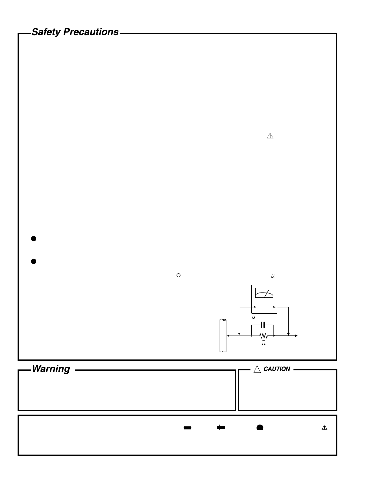
5. Leakage current check (Electrical shock hazard testing)
After re-assembling the product, always perform an isolation check on the exposed metal parts of the product
(antenna terminals, knobs, metal cabinet, screw heads, headphone jack, control shafts, etc.) to be sure the
product is safe to operate without danger of electrical shock.
Do not use a line isolation transformer during this check.
Plug the AC line cord directly into the AC outlet. Using a "Leakage Current Tester", measure the leakage
current from each exposed metal parts of the cabinet, particularly any exposed metal part having a return
path to the chassis, to a known good earth ground. Any leakage current must not exceed 0.5mA AC (r.m.s.).
Alternate check method
Plug the AC line cord directly into the AC outlet. Use an AC voltmeter having, 1,000 ohms per volt or more
sensitivity in the following manner. Connect a 1,500 10W resistor paralleled by a 0.15 F AC-type capacitor
between an exposed metal part and a known good earth ground.
Measure the AC voltage across the resistor with the AC
voltmeter.
Move the resistor connection to each exposed metal part,
particularly any exposed metal part having a return path to
the chassis, and measure the AC voltage across the resistor.
Now, reverse the plug in the AC outlet and repeat each
measurement. Voltage measured any must not exceed 0.75 V
AC (r.m.s.). This corresponds to 0.5 mA AC (r.m.s.).
0.15 F AC TYPE
1500 10W
Good earth ground
AC VOLTMETER
(Having 1000
ohms/volts,
or more sensitivity)
Place this
probe on
each exposed
metal part.
!
1. This equipment has been designed and manufactured to meet international safety standards.
2. It is the legal responsibility of the repairer to ensure that these safety standards are maintained.
3. Repairs must be made in accordance with the relevant safety standards.
4. It is essential that safety critical components are replaced by approved parts.
5. If mains voltage selector is provided, check setting for local voltage.
Burrs formed during molding may
be left over on some parts of the
chassis. Therefore, pay attention to
such burrs in the case of
preforming repair of this system.
In regard with component parts appearing on the silk-screen printed side (parts side) of the PWB diagrams, the
parts that are printed over with black such as the resistor ( ), diode ( ) and ICP ( ) or identified by the " "
mark nearby are critical for safety.
When replacing them, be sure to use the parts of the same type and rating as specified by the manufacturer.
(Except the J and C version)
1-2
Page 3
XV-FA90BK/XV-FA92SL/XV-FA95GD
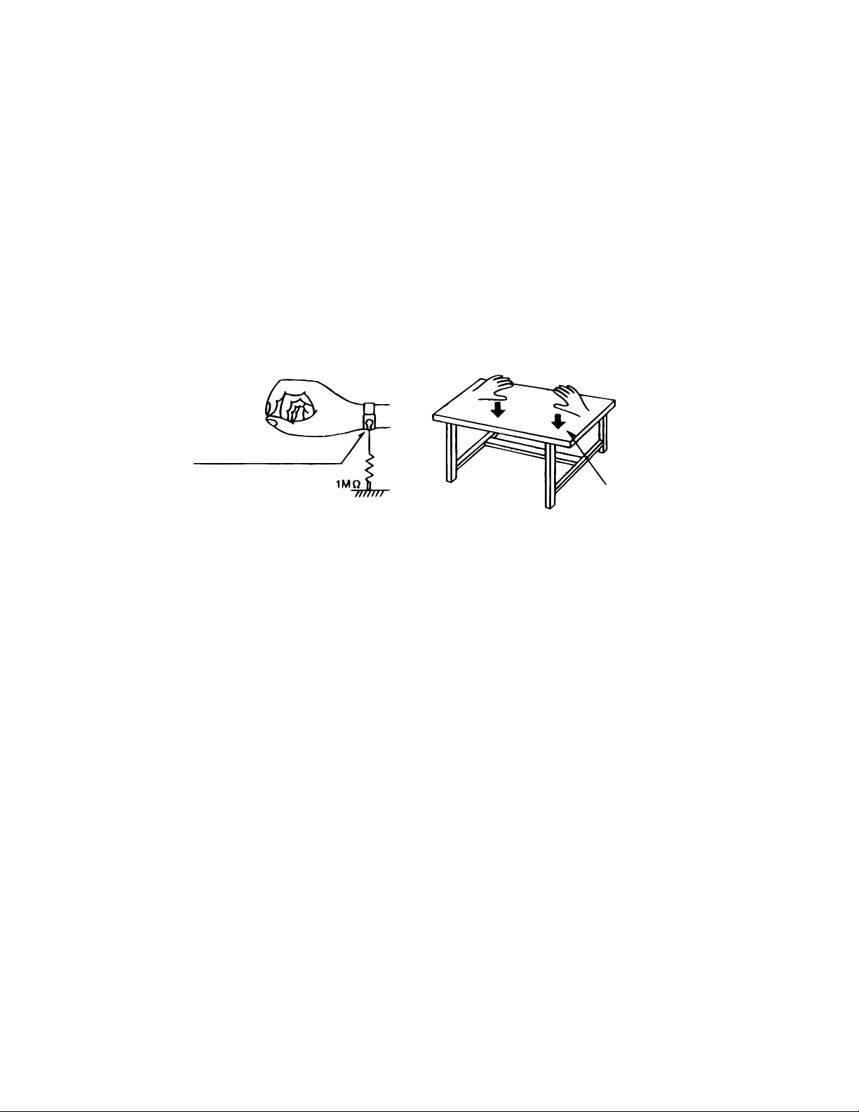
Preventing static electricity
Electrostatic discharge (ESD), which occurs when static electricity stored in the body, fabric, etc. is discharged,
can destroy the laser diode in the traverse unit (optical pickup). Take care to prevent this when performing repairs.
1.1. Grounding to prevent damage by static electricity
Static electricity in the work area can destroy the optical pickup (laser diode) in devices such as DVD players.
Be careful to use proper grounding in the area where repairs are being performed.
1.1.1. Ground the workbench
1. Ground the workbench by laying conductive material (such as a conductive sheet) or an iron plate over
it before placing the traverse unit (optical pickup) on it.
1.1.2. Ground yourself
1. Use an anti-static wrist strap to release any static electricity built up in your body.
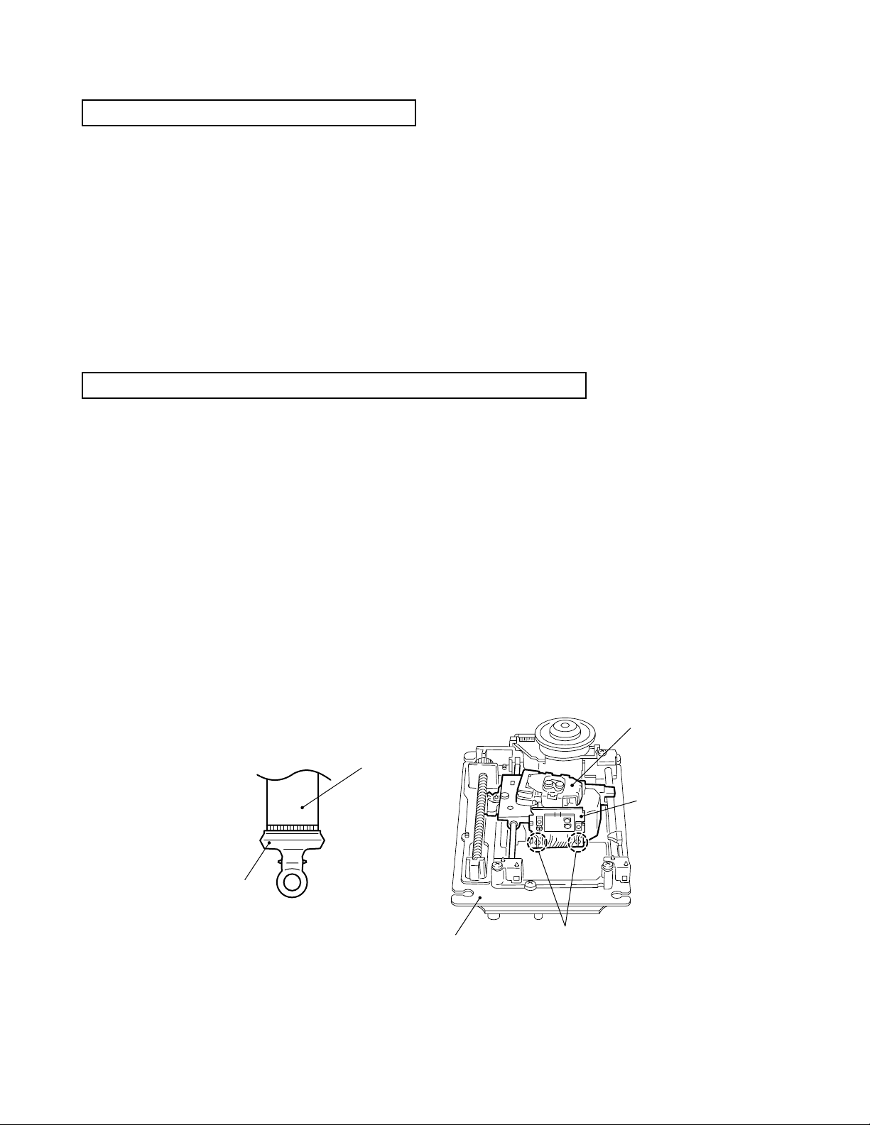
(caption)
Anti-static wrist strap
Conductive material
(conductive sheet) or iron plate
1.1.3. Handling the optical pickup
1. In order to maintain quality during transport and before installation, both sides of the laser diode on the
replacement optical pickup are shorted. After replacement, return the shorted parts to their original condition.
(Refer to the text.)
2. Do not use a tester to check the condition of the laser diode in the optical pickup. The tester's internal power
source can easily destroy the laser diode.
1.2. Handling the traverse unit (optical pickup)
1. Do not subject the traverse unit (optical pickup) to strong shocks, as it is a sensitive, complex unit.
2. Cut off the shorted part of the flexible cable using nippers, etc. after replacing the optical pickup. For specific
details, refer to the replacement procedure in the text. Remove the anti-static pin when replacing the traverse
unit. Be careful not to take too long a time when attaching it to the connector.
3. Handle the flexible cable carefully as it may break when subjected to strong force.
4. It is not possible to adjust the semi-fixed resistor that adjusts the laser power. Do not turn it
1-3
Page 4
XV-FA90BK/XV-FA92SL/XV-FA95GD
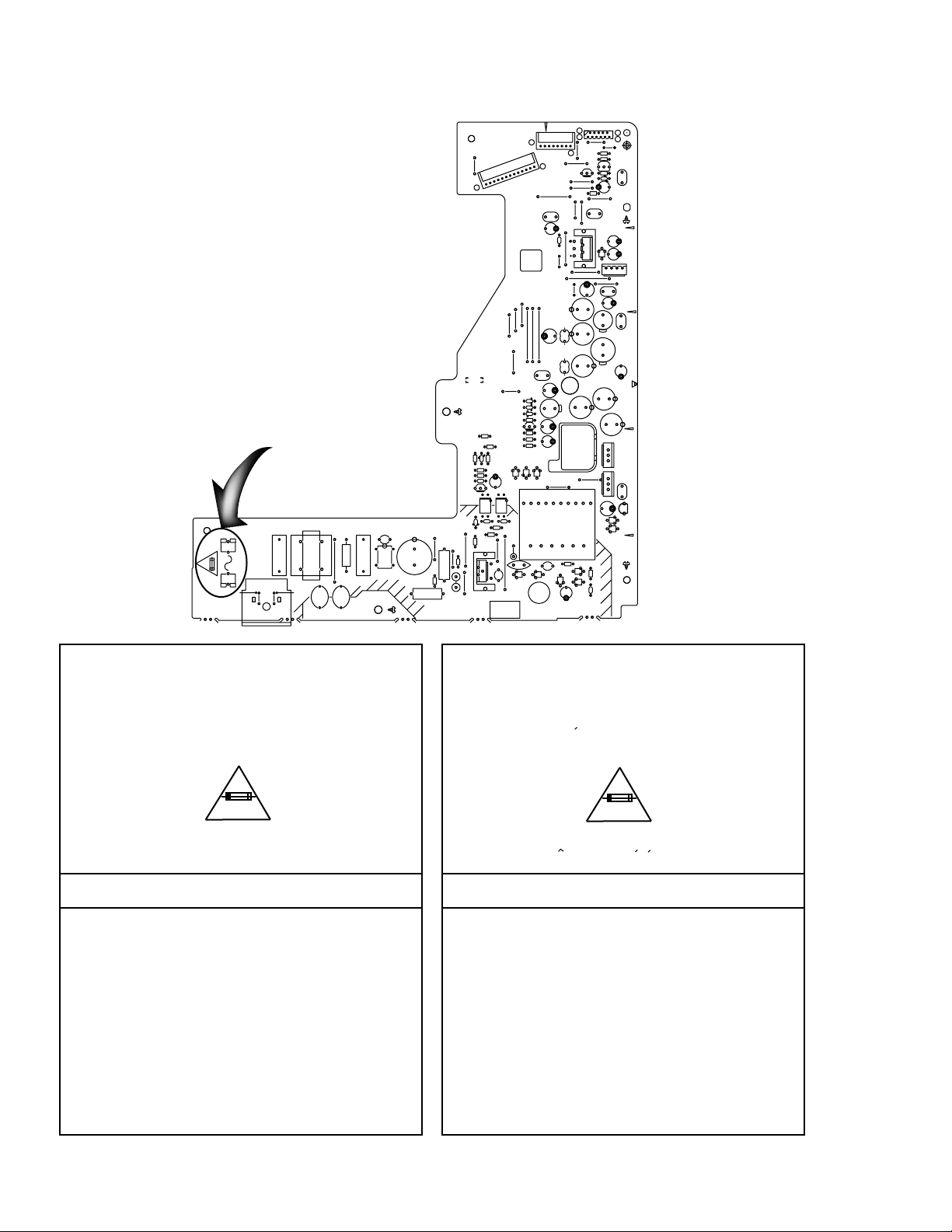
Importance Admistering point on the Safety
CN952
B204
B316
Q952
B314
B313
R955
B504
C973
B203
B311
C970
B503
C994
IC952
B106
B310
B502
B104
C984
L959
C989
B802
B803
B804
C987
C981
L957
C997
C982
C979
L955
C995
C996
D954
B304
D908
R903
C909
D902
D904
D910
C914
C902 C903
F901
J901
FC901 FC902
B101
B205
B308
B307
B306
B341
B202
D974
D972
D973
R976
Q953
R963
R974
R975
R900
R973
D991
R965
R969
D956
R961
R960
C993
Q991
L901
B102
C905 C906
C919
R902
B701
C907
D901
R905
D911
R911
R907
B301
B201
B501
C915
HS901
R906
B302
K902
D957
C992
PC901
PC902
C917
C918
R908
R910
R901
B303
B801
C908
IC901
D903
C913
CN951
B320
B103
R956
R952
Q951
R953
D960
C951
C962
B312
C968
HS952
C978
D950
C969
IC951
B309
C967
C972
C966
C961
L952
L951
C960
C965
C971
D958
B305
D953
C964
C963
CP951
D951
D952
T901
R904
C910
Full Fuse Replacement Marking
Graphic symbol mark
(This symbol means fast blow type fuse.)
should be read as follows ;
FUSE CAUTION
FOR CONTINUED PROTECTION AGAINST RISK
OF FIRE, REPLACE ONLY WITH SAME TYPE
AND RATING OF FUSES ;
F901 : 1.6 A / 125 V F901 : 1.6 A / 125 V
Marquage Pour Le Remplacement
Complet De Fusible
Le symbole graphique (Ce symbole signifie
fusible de type a fusion rapide.)
doit etre interprete comme suit ;
PRECAUTIONS SUR LES FUSIBLES
POUR UNE PROTECTION CONTINUE CONTRE
DES RISQUES D'INCENDIE, REMPLACER
SEULEMENT PAR UN FUSIBLE DU MEME TYPE ;
1-4
Page 5
XV-FA90BK/XV-FA92SL/XV-FA95GD
Precautions for Service
Handling of Traverse Unit and Laser Pickup
1. Do not touch any peripheral element of the pickup or the actuator.
2. The traverse unit and the pickup are precision devices and therefore must not be subjected to
strong shock.
3. Do not use a tester to examine the laser diode. (The diode can easily be destroyed by the
internal power supply of the tester.)
4. To replace the traverse unit, pull out the metal short pin for protection from charging.
5. When replacing the pickup, after mounting a new pickup, remove the solder on the short land
which is provided at the center of the flexible wire to open the circuit.
6. Half-fixed resistors for laser power adjustment are adjusted in pairs at shipment to match the
characteristics of the optical block.
Do not change the setting of these half-fixed resistors for laser power adjustment.
Destruction of Traverse Unit and Laser Pickup by Static Electricity
Laser diodes are easily destroyed by static electricity charged on clothing
or the human body. Before repairing peripheral elements of the traverse
unit or pickup, be sure to take the following electrostatic protection:
1. Wear an antistatic wrist wrap.
2. With a conductive sheet or a steel plate on the workbench on which
the traverse unit or the pick up is to be repaired, ground the sheet
or the plate.
3. After removing the flexible wire from the connector (CN101),
short-circuit the flexible wire by the metal clip.
4. Short-circuit the laser diode by soldering the land which is provided
at the two places of the flexible board for the pickup.
After completing the repair, remove at the two places of the solder to open the circuit.
Flexible wire
Metal clip
Pickup unit
Flexible board
Traverse mechanism unit
Land (Soldering two places)
1-5
Page 6
XV-FA90BK/XV-FA92SL/XV-FA95GD
Disassembly method
<Main body>
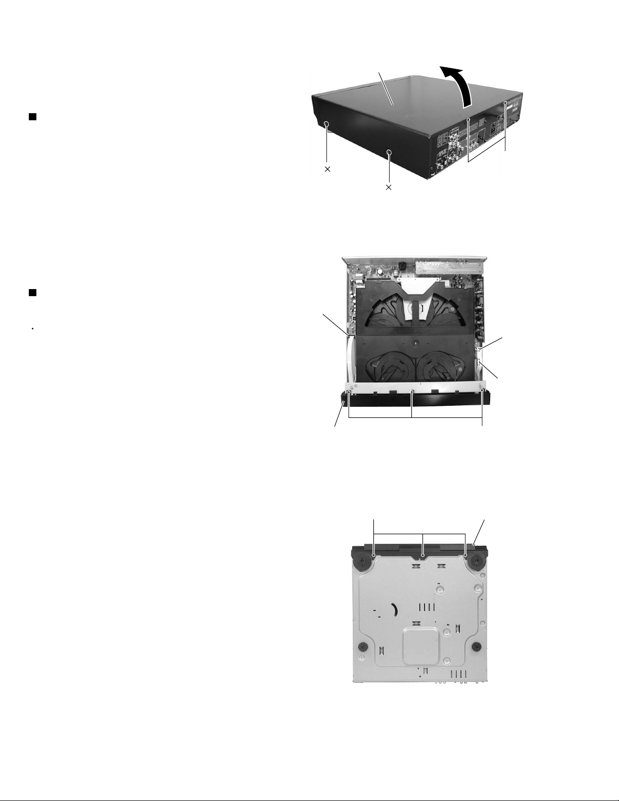
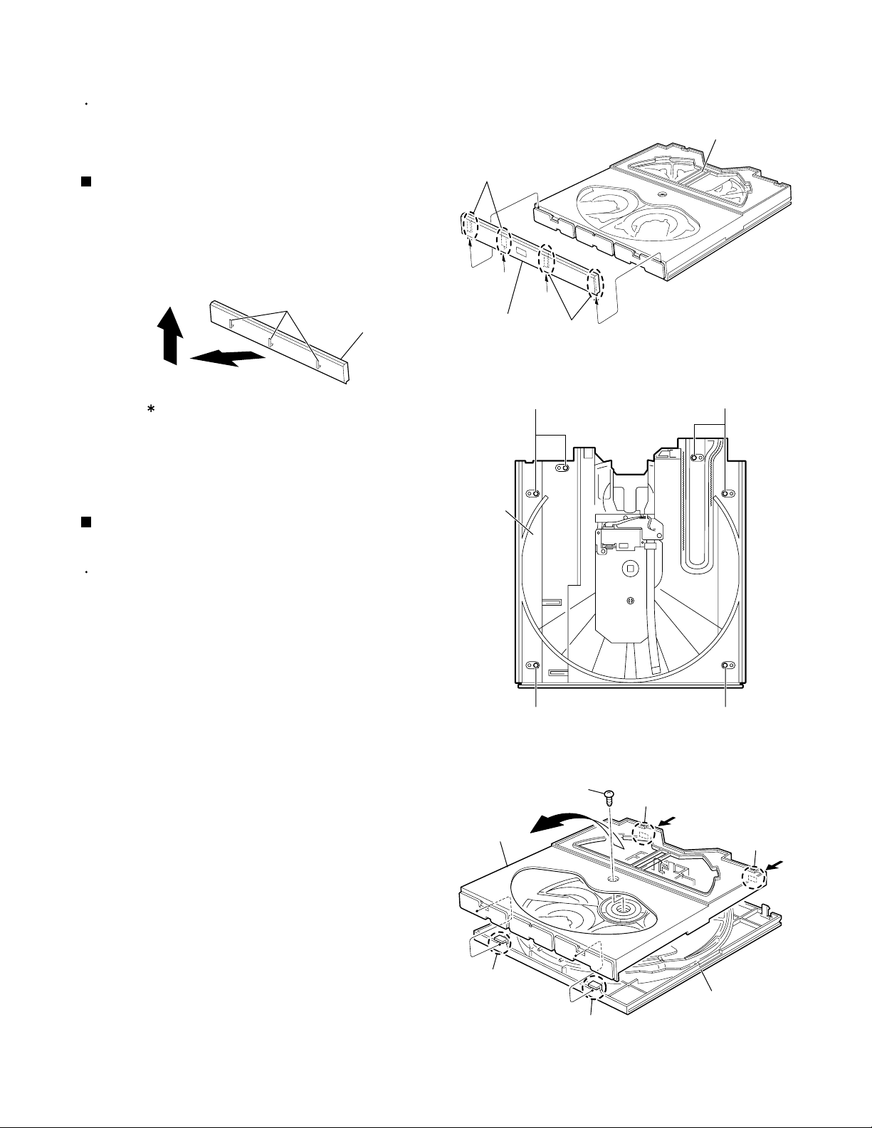
Removing the top cover (See Fig.1)
1.
Remove the four screws A on each side of the body.
2.
Remove the two screws B on the back of the body.
3.
Lift the rear part of the top cover and remove in the
direction of the arrow while pulling both sides of the
top cover outward.
Removing the front panel assembly
(See Fig.2 and 3)
Prior to performing the following procedure, remove
the top cover.
A
2
Power board
CN951
Top cover
A
B
2
Fig.1
Servo control
board
CN801
1.
Disconnect the card wire from connector CN801 and
,
CN803 on the servo control board
the power board respectively.
2.
Remove the three screws C on the upper side of the
body.
3.
Remove the three screws D on the bottom of the
body.
Remove the front panel assembly toward the front.
and CN951 on
Front panel assembly
D
CN803
C
Fig.2
Front panel assembly
(Bottom)
1-6
Fig.3
Page 7
XV-FA90BK/XV-FA92SL/XV-FA95GD
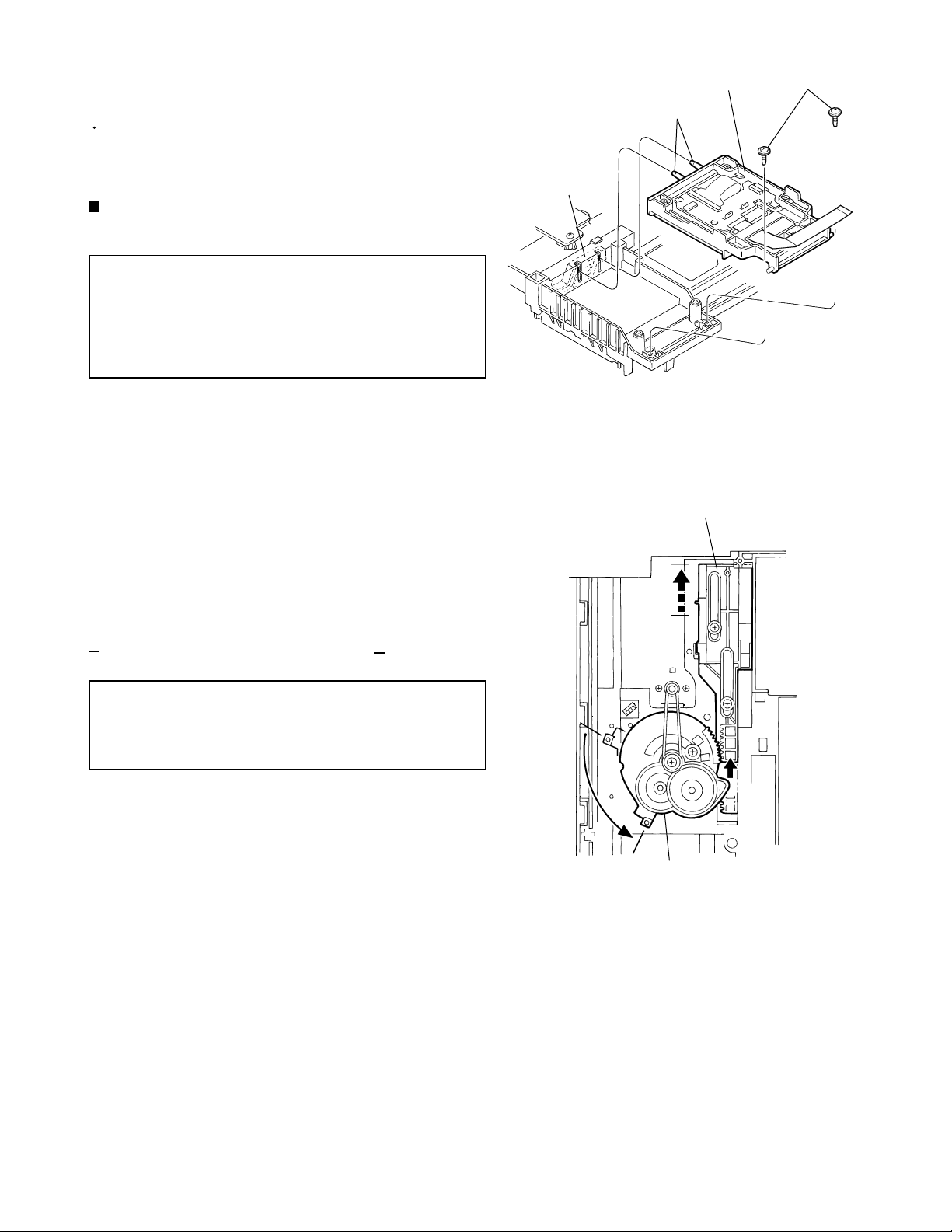
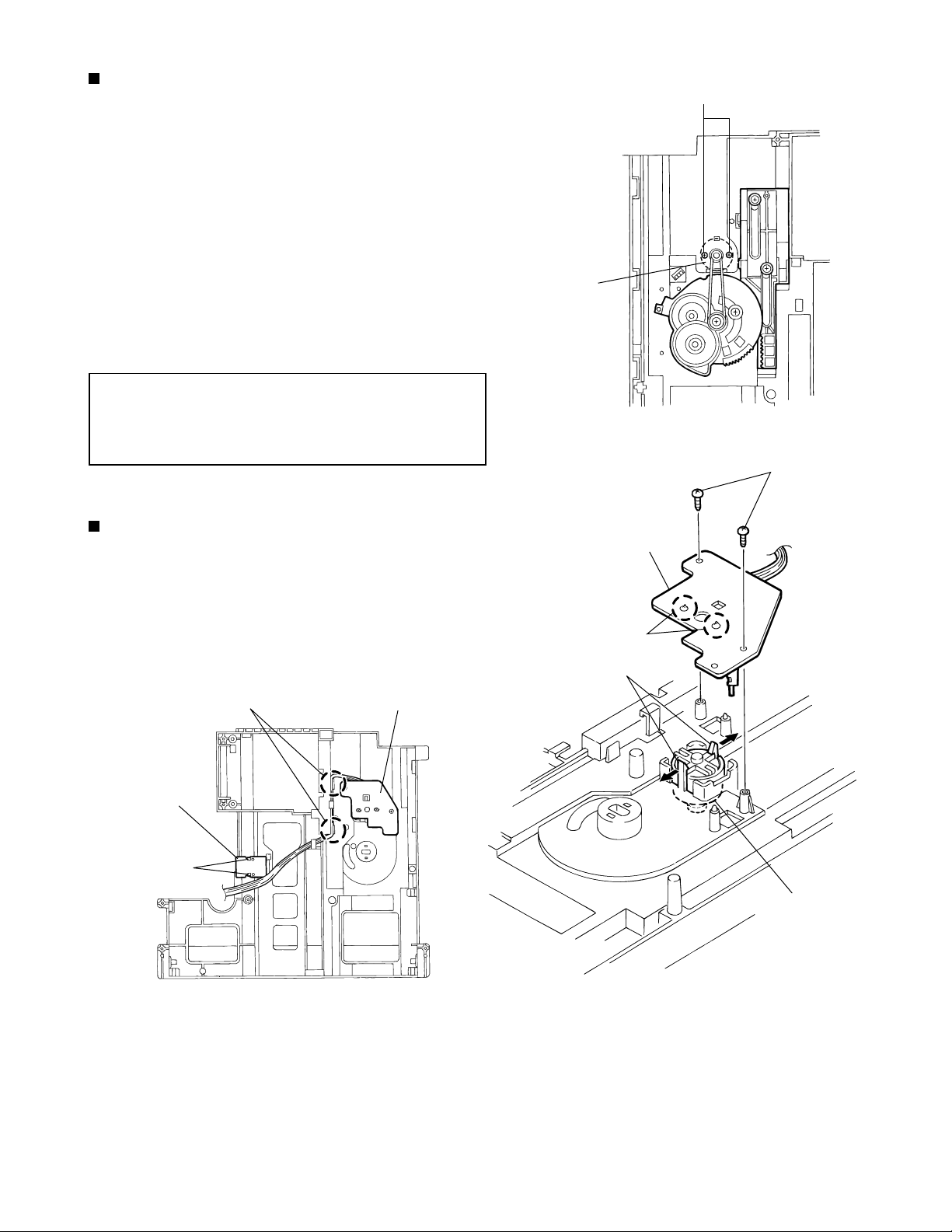
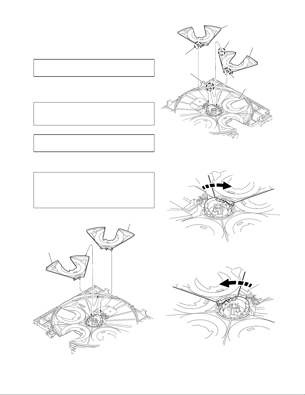
Removing the main tray assembly
(See Fig.4 to 7)
Prior to performing the following procedure, remove
the top cover and the front panel assembly.
1.
Turn over the body and insert a screwdriver into the
slot of the bottom chassis, then move it in the
direction of the arrow in Fig.4. The main tray
assembly will move forward.
2.
Draw the main tray assembly toward the front
manually.
3.
Bring up the joint a over the boss of the loading base
assembly, and remove the main tray assembly
toward the front.
4.
Disconnect the card wire, on the back of the main
tray assembly, from connector CN841 on the relay
board 1.
Main tray assembly
Bottom chassis
(slot)
Fig.4
Joint a
Card wire
Main tray assembly
Loading base assembly
Bottom chassis
Fig.5
Relay board 1
CN841
Joint a
Loading base
assembly
Boss
Relay board 1
Main tray assembly
Fig.6Fig.7
1-7
Page 8
XV-FA90BK/XV-FA92SL/XV-FA95GD
Reattaching the main tray assembly
(See Fig.8 to 10)
1.
Turn over the main tray assembly and pass the card
wire extending from the photo sensor board through
the notch b, in advance (Fig.8).
2.
From above the loading base assembly, turn the
load base counterclockwise until the slide gear stops
at the back end (Bring down the traverse mechanism
assembly).
3.
Reattach the main tray assembly to the loading base
assembly while fitting to the groove on the right and
left sides of the loading base assembly.
4.
Connect the card wire through the notch b to
connector CN841 on the relay board 1.
5.
Reattach the main tray assembly while fitting the slot
c to the shaft.
Main tray assembly
Photo sensor board
Loading base assembly
Load base
Notch b
Fig.8
Slide gear
Removing the loading base assembly
(See Fig.11)
Prior to performing the following procedure, remove
the top cover, the front panel assembly and the main
tray assembly.
1.
Disconnect the wire from connector CN808, CN809
and the card wire from CN210 on the servo control
board respectively.
2.
Remove the seven screws E attaching the loading
base assembly.
Joint a
Boss
Relay board 1
CN841
Loading base assembly
E
E
Fig.9
Slot c
Shaft
Fig.10
E
Servo control board
CN210
CN808
CN809
E
E
Fig.11
1-8
Page 9
Removing the rear panel (See Fig.12)
Prior to performing the following procedure, remove
the top cover.
1.
Remove the fourteen screws F attaching the rear
panel.
XV-FA90BK/XV-FA92SL/XV-FA95GD
FF
F
Removing each board (See Fig.13,14)
Prior to performing the following procedure, remove
the top cover, the front panel assembly, the main
tray assembly, rear panel and the loading base
assembly.
Surround audio board
Pull out the surround audio terminal board from
1.
connector CN763.
Remove the screw G attaching the surround audio
2.
board.
Pull out the surround audio board from connector
3.
CN754 and CN603.
Servo control board
Pull out the relay board 2 on the upper side of the
1.
body.
Disconnect the wire from connector CN807, CN810
2.
and CN901 on the servo control board respectively.
Lug wire
Relay board 1
Power
board
I
F
CN842
F
Fig.12
Relay board 2
CN901
H
Fig.13
CN807
Rear panel
Surround audio
terminal board
CN763
CN754
A/V output board
G
H
CN603
Surround audio board
Servo control
board
H
CN810
Remove the screw I attaching the lug wire.
3.
Remove the three screws H attaching the servo
4.
control board.
Relay board 1
1.
Disconnect the wire from connector CN842 on the
relay board 1.
2.
Remove the two screws I attaching the relay board.
A/V output board
1.
Pull out the relay board 2 on the upper side of the body.
2.
Remove the four screws J attaching the A/V output
board.
Power board
1.
Disconnect the wire from connector CN952 and
CN953 on the power board.
2.
Remove the four screws K on the upper side of the
body.
Power board
K
CN952
CN953
K
Relay board 1
Fig.14
A/V output board
J
J
Relay board 2
Servo control
board
1-9
Page 10
XV-FA90BK/XV-FA92SL/XV-FA95GD
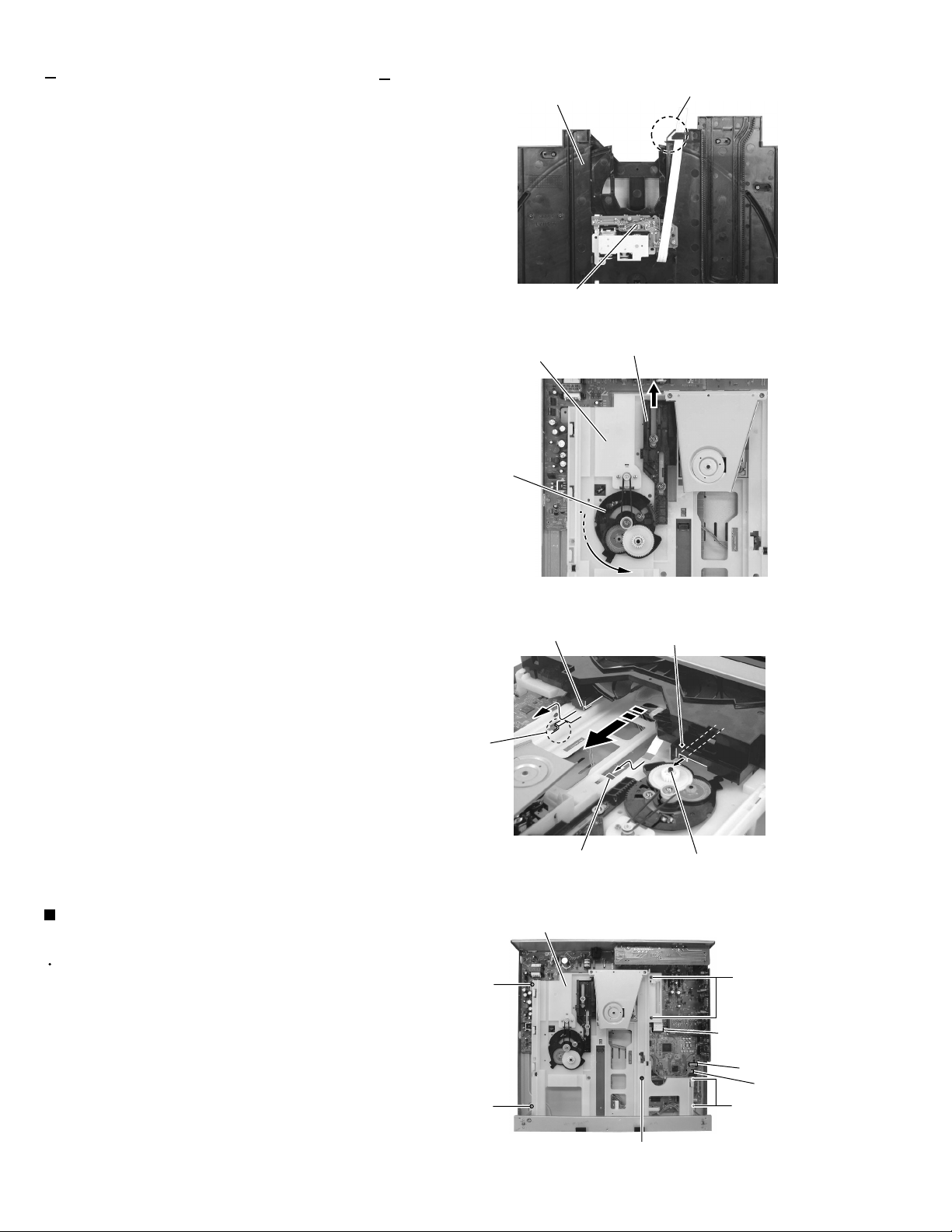
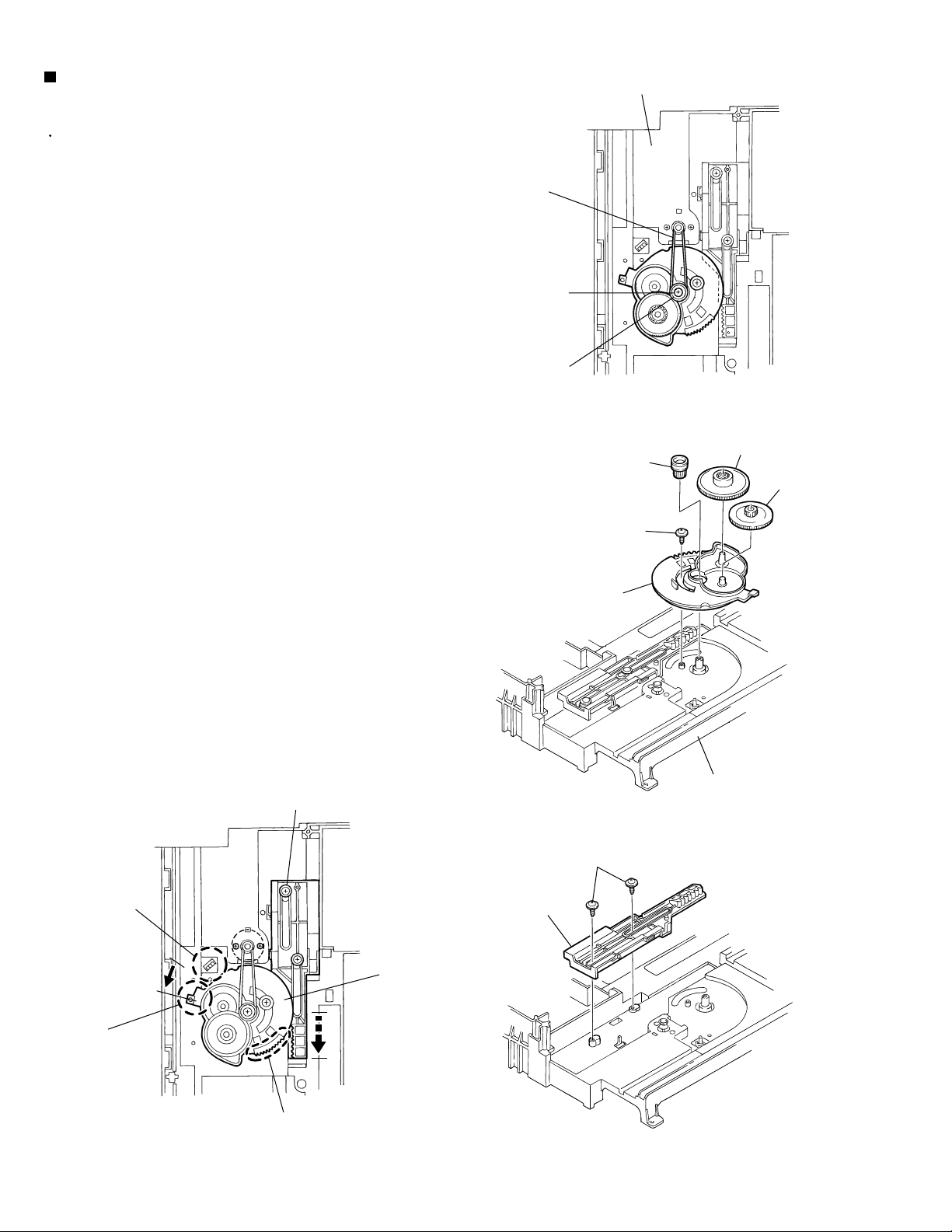
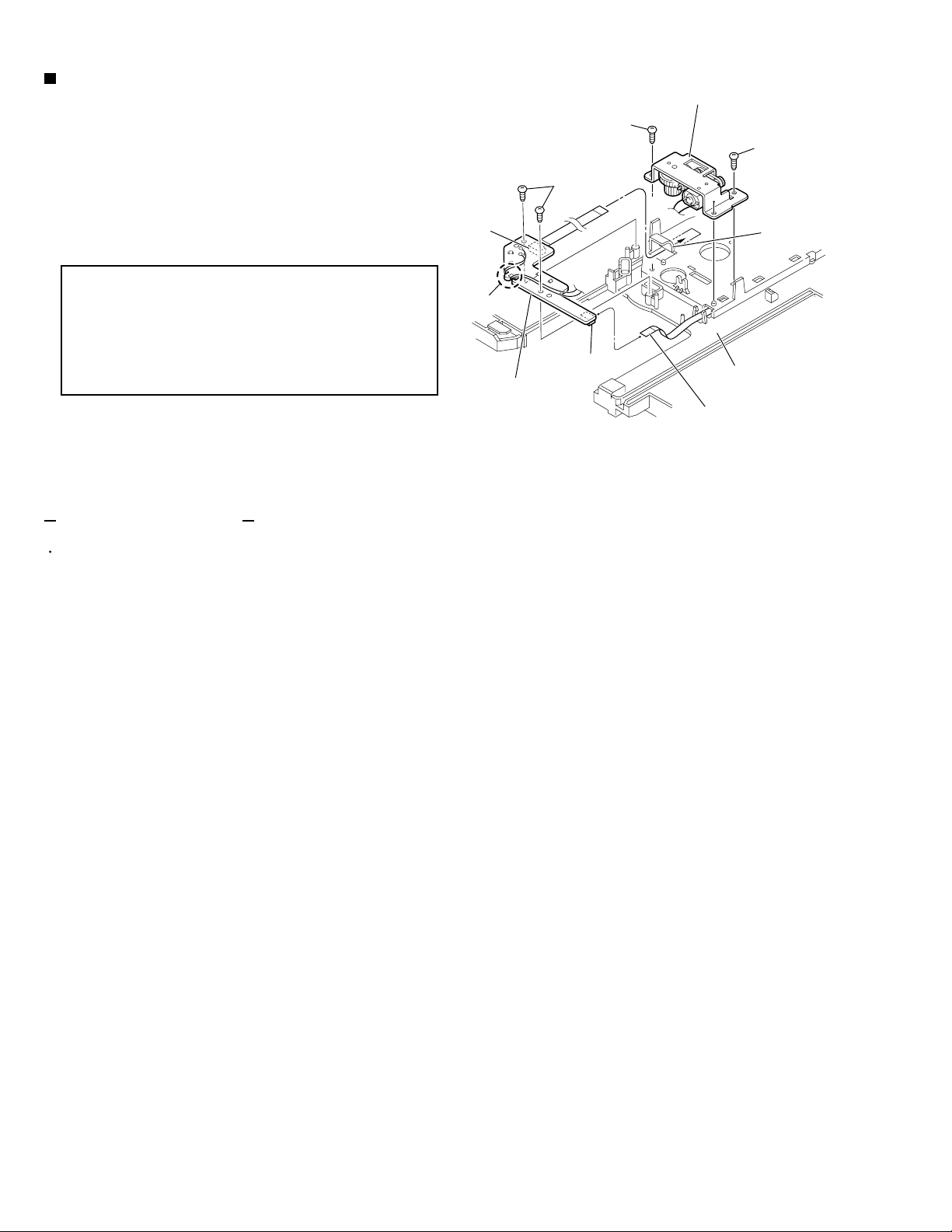
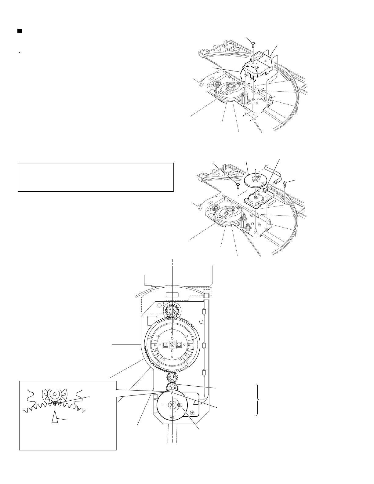
Removing the traverse mechanism
assembly (See Fig.15 and 16)
Prior to performing the following procedure, remove
the top cover and the front panel assembly.
REFERENCE:
1.
Eject the main tray assembly toward the front
referring to “Removing the main tray assembly”.
2.
Remove the two screws L and pull out the clamper
base assembly upward.
3.
Disconnect the card wire from connector CN210 on
the servo control board.
4.
Remove the four screws M and the traverse
mechanism assembly upward.
CAUTION:
There is no need to remove the loading
base assembly.
When reattaching the traverse mechanism
assembly, pass the card wire extending
from the traverse mechanism assembly
through the notch d of the elevator base.
Clamper base
assembly
L
L
M
Servo control board
CN210
Fig.15
Notch d
Servo control board
CN210
<Front panel assembly>
Prior to performing the following procedure, remove
the top cover and the front panel assembly.
Removing the power switch board
(See Fig.17)
1.
Remove the two screws N on the back of the front
panel assembly.
2.
Disconnect the card wire from connector CN813 and
CN806 on the power switch board.
Removing the operation switch board
(See Fig.17)
1.
Remove the six screws O on the back of the front
panel assembly.
2.
Disconnect the card wire from connector CN812 on
the operation switch board.
Removing the FL display board
(See Fig.17)
1.
Remove the two screws P on the back of the front
panel assembly.
Traverse mechanism
assembly
Operation switch board
OO
OP
FL display board
M
Fig.16
Fig.17
CN805
CN813
CN812
CN806
Power switch board
N
2.
Disconnect the card wire from connector CN805 on
the FL display board.
1-10
Page 11
XV-FA90BK/XV-FA92SL/XV-FA95GD
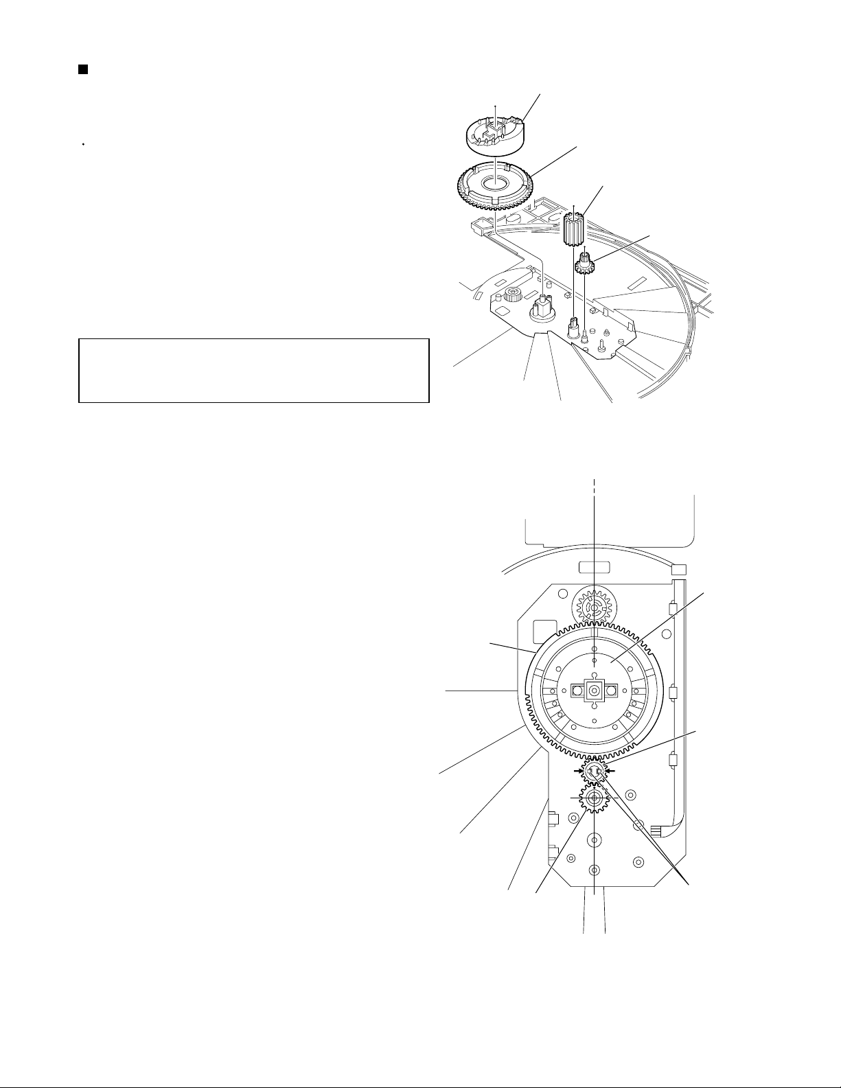
<Loading base assembly unit>
Prior to performing the following procedures, remove
the top cover, the front panel assembly, the main
tray assembly, the loading base assembly.
Removing the elevator base
(See Fig.18 and 19)
REFERENCE:
1.
Turn over the loading base assembly and remove
the two screws Q.
2.
Remove the elevator base upward.
It is not necessary to remove the traverse
mechanism assembly from the elevator
base. As the removing procedure of the
traverse mechanism, please refer to
“Removing the traverse mechanism
assembly”.
Slide gear
Elevator base
Shafts
Fig.18
Slide gear
Q
Reattaching the elevator base
REFERENCE:
1.
Reattach the elevator base to the loading base
assembly while fitting the two shafts on the side of
the elevator base to the grooves of the slide gear.
2.
Reattach the two screws Q.
From above the loading base, turn the
load base counterclockwise until the slide
gear stops at the back end as shown in
Fig.19.
Load base
Fig.19
1-11
Page 12
XV-FA90BK/XV-FA92SL/XV-FA95GD
Removing the belt / load base / slide
gear
Prior to performing the following procedures, remove
the elevator base.
1.
Remove the belt on the upper side of the loading
base assembly.
2.
Remove the screw R attaching the pulley gear.
3.
Remove the pulley gear, the gear 1, the gear 2 and
the belt respectively.
4.
Remove the screw S and the load base upward.
5.
Remove the two screws T and the slide gear
upward.
CAUTION: When reattaching the slide gear
and the load base,
1.
Move the slide gear toward the front until it stops
(Fig.23).
Loading base assembly
Belt
R
Pulley gear
Fig.20
Gear 2
Pulley gear
Gear 1
S
2.
Make sure that the part d of the load base is out of
alignment with the switch e and that the gear f is
disengaged from the slide gear.
Slide gear
Switch e
Load base
Load base
Loading base assembly
Fig.21
T
Slide gear
1-12
Part d
Gear f
Fig.22Fig.23
Page 13
XV-FA90BK/XV-FA92SL/XV-FA95GD
Removing the loading motor / loading
motor board (See Fig.24 and 25)
1.
Remove the two screws U attaching the loading
motor on the upper side of the loading base
assembly.
2.
Turn over the loading base assembly and unsolder
the two soldering g on the loading motor board.
3.
Remove the two screws V attaching the loading
motor board.
4.
Spread apart the two tabs h and pull out the loading
motor.
CAUTION:
When reattaching the loading motor board,
settle the wires on the two hooks i on the
loading base assembly and draw the other
end to the left as shown in Fig.26.
Removing the tray switch board
(See Fig.26)
U
Loading motor
Fig.24
V
Loading motor board
1.
Turn over the loading base assembly, and remove
the tray switch board while spreading apart the two
tabs j.
Hooks i
Tray switch board
Tabs j
Loading motor board
Soldering g
Tabs h
Loading motor
Fig.25Fig.26
1-13
Page 14
XV-FA90BK/XV-FA92SL/XV-FA95GD
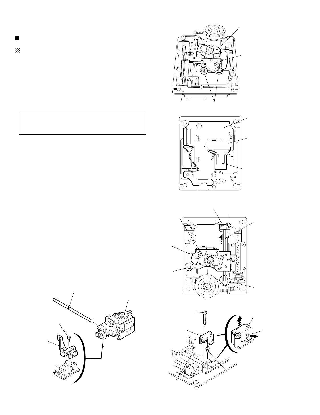
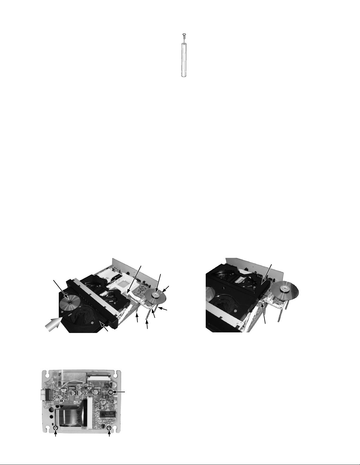
<Traverse mechanism unit>
Removing the pickup (See Fig.1 to 5)
It is not necessary to remove the traverse
mechanism unit.
1.
Solder soldering a on the flexible board next to the
pickup unit.
2.
From the bottom of the traverse mechanism unit,
disconnect the flexible wire from CN101 on the
pickup board.
ATTENTION:
3.
Remove the screw A attaching the shaft stopper (R)
on the upper side of the traverse mechanism unit.
Pull the side of the shaft stopper (R) outward to
release the joint b and remove it upward. Remove
the skew spring at the same time.
Disconnecting the flexible wire without
soldering may cause damage to the
pickup.
Traverse mechanism unit
Pickup unit
Flexible board
Soldering a
Fig.1
Pickup board
CN101
Flexible wire
4.
Move the shaft in the direction of the arrow to release
it from the part c.
5.
Release the joint d with the shaft and remove the
pickup with the shaft.
6.
Pull out the shaft.
7.
Remove the screw B attaching the switch actuator.
Shaft
Pickup
B
Switch actuator
Pickup unit
Shaft
Joint d
Shaft stopper (R)
Fig.2
Shaft stopper (R)
Fig.3
A
A
Shaft
Part c
Shaft stopper (R)
Joint b
1-14
Fig.5
Skew spring
Shaft
Fig.4
Page 15
XV-FA90BK/XV-FA92SL/XV-FA95GD
Removing the pickup board
(See Fig.1 and 6)
It is not necessary to remove the traverse
mechanism unit.
1.
Solder soldering a on the flexible board next to the
pickup unit.
2.
From the bottom of the traverse mechanism unit,
disconnect the flexible wire from CN101 on the
pickup board.
ATTENTION:
3.
Disconnect the card wire from connector CN201 on
the pickup board and unsolder the soldering e and f
on the harnesses
4.
Remove the screw C attaching the pickup board and
release the two joints g.
Disconnecting the flexible wire without
soldering may cause damage to the
pickup.
Traverse mechanism unit
Joint g
Feed motor
assembly
Pickup unit
Flexible board
Soldering a
Fig.1
Pickup board
C
CN101
Removing the feed motor assembly
(See Fig.1, 6 and 7)
Prior to performing the following procedure, remove
the traverse mechanism unit.
1.
Solder soldering a on the flexible board next to the
pickup unit.
2.
From the bottom of the traverse mechanism unit,
disconnect the flexible wire from CN101 on the
pickup board.
ATTENTION:
3.
Remove the pickup board.
4.
Remove the two screws D attaching the feed motor
assembly and remove the thrust spring. Move the
feed motor assembly in the direction of the arrow to
pull it out from the feed holder.
Disconnecting the flexible wire without
soldering may cause damage to the
pickup.
Soldering f
Feed holder assembly
Soldering e
Feed motor assembly
CN201
Fig.6
Thrust spring
D
D
Fig.7
1-15
Page 16
XV-FA90BK/XV-FA92SL/XV-FA95GD
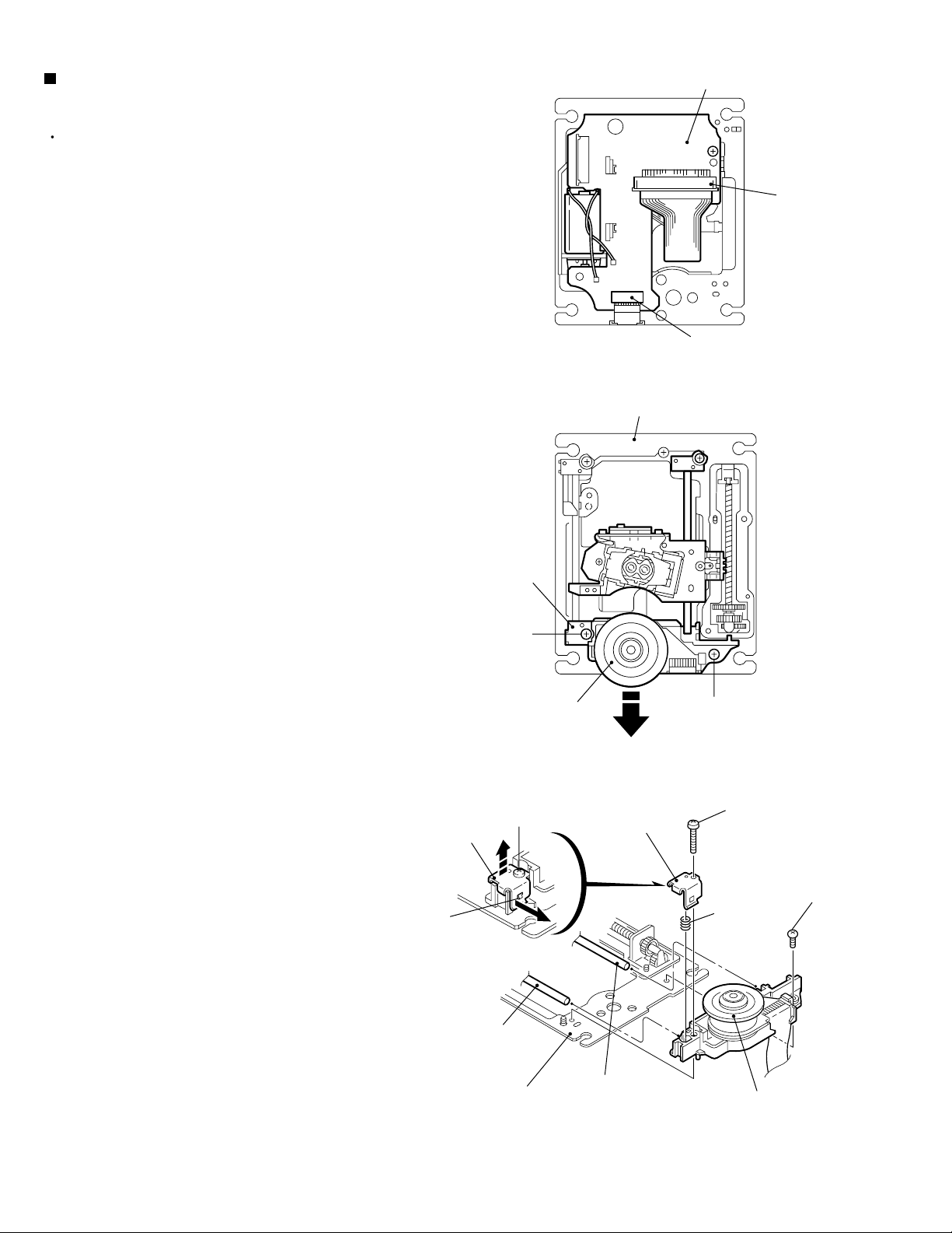
Removing the turn table assembly
(See Fig.6, 8 and 9)
Prior to performing the following procedure, remove
the traverse mechanism unit.
1.
Disconnect the card wire extending from the turn
table assembly, from connector CN201 on the pickup
board.
2.
Remove the screw E attaching the shaft stopper (F)
on the upper side of the traverse mechanism unit.
Pull the side of the shaft stopper (F) outward to
release the joint h and remove it upward. Remove
the spring at the same time.
3.
Remove the screw F attaching the turn table
assembly.
4.
Move the turn table assembly outward and pull out
from the shaft. Then remove it from the base chassis.
Pickup board
CN101
CN201
Fig.6
Traverse mechanism unit
Shaft stopper (F)
Turn table assembly
Shaft stopper (F)
Joint h
E
E
F
Fig.8
E
Shaft stopper (F)
F
Spring
1-16
Shaft
Base chassis
Shaft
Turn table assembly
Fig.9
Page 17
<Main tray assembly unit>
Prior to performing the following procedures, remove
the top cover, the front panel assembly and the main
tray assembly.
XV-FA90BK/XV-FA92SL/XV-FA95GD
Main tray assembly
Removing the fitting (See Fig.1)
1.
Remove the fitting on the front side of the main tray
assembly while releasing the four joints a upward.
Hook
Fitting
Lifts for above while pulling the hook
in three places to front side.
Removing the main tray cover and the
main tray (See Fig.2 and 3)
Prior to performing the following procedure, remove
the fitting.
Joints a
Fitting
Main tray
assembly
Joints a
Fig.1
AA
1.
Remove the six screws A attaching the main tray
on the under side of the main tray assembly.
2.
Remove the screw B attaching the main tray cover
on the upper side of the main tray assembly.
3.
Push the two joint tabs b on the back of the main
tray assembly to release the main tray cover from
the tray bottom. Disengage the joint tabs c of the
main tray from the main tray cover.
Main tray cover
Joint tab c
AA
Fig.2
B
Joint tab c
Joint tab b
Joint tab b
Main tray
Fig.3
1-17
Page 18
XV-FA90BK/XV-FA92SL/XV-FA95GD
Removing the photo sensor board and
the sub tray drive motor assembly
(See Fig.4)
1.
Turn over the main tray assembly and remove the
two screws C attaching the photo sensor board.
2.
Disconnect the card wire from connector CN082 on
the photo sensor board.
CN081
Sub tray drive motor assembly
D
D
C
Notch e
REFERENCE:
3.
Remove the two screws D attaching the sub tray
drive motor assembly.
Make sure to disconnect the card wire
from the photo sensor board. If the
photo sensor board is pulled out from
the main tray without disconnecting the
card wire, the cam switch side inside of
the main tray may be damaged.
When reassembling,
Attach the two wires to the part d on the photo
sensor board, and before reattaching the photo
sensor board, connect the card wire to connector
CN082 and pass the card wire extending from
connector CN081 through the notch e of the main
tray.
Part d
Photo sensor board
CN082
Main tray
Card wire
Fig.4
1-18
Page 19
XV-FA90BK/XV-FA92SL/XV-FA95GD
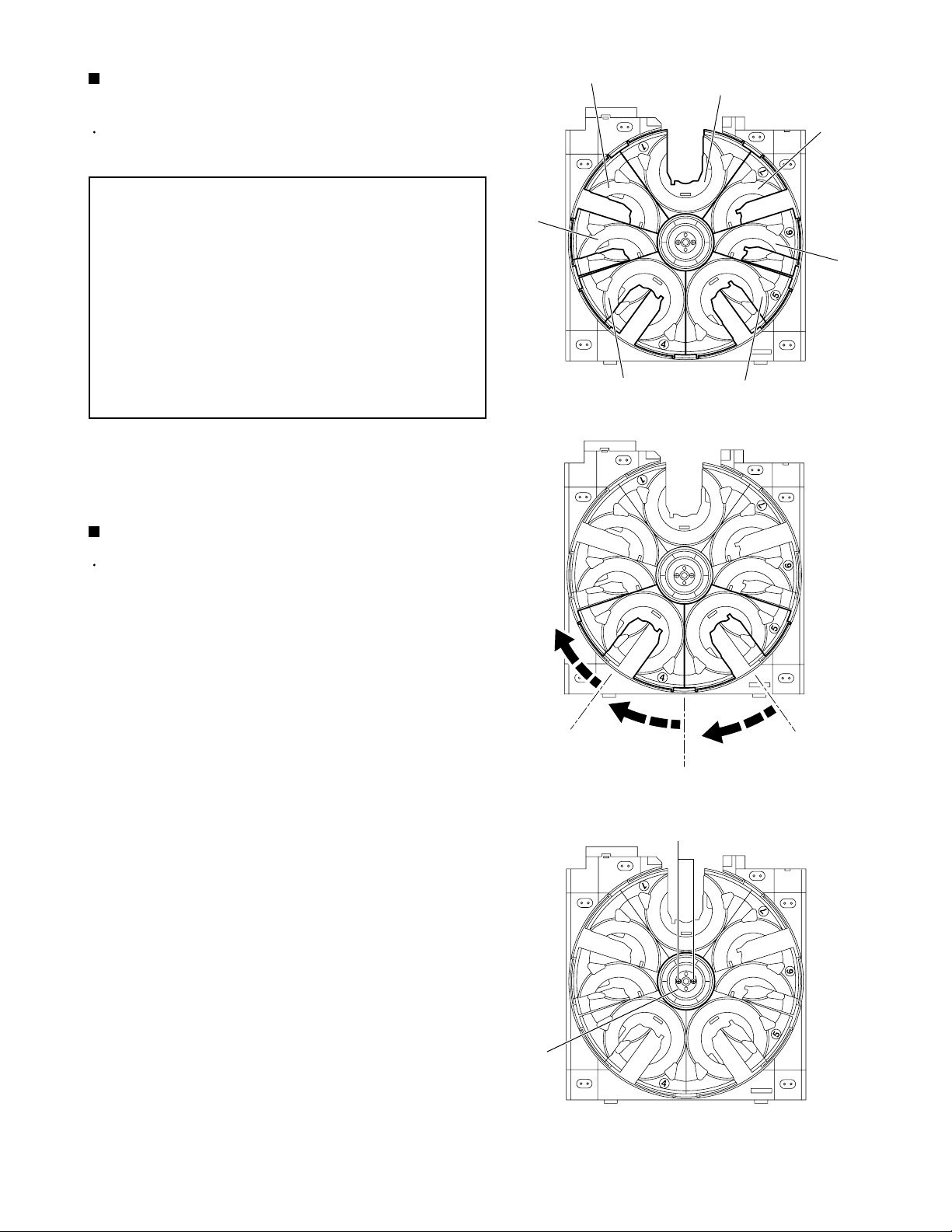
Sub tray position and operation check
(See Fig.5 and 6)
Prior to performing the following procedures, remove
the fitting and the main tray cover.
CAUTION:
Make sure the sub trays are set as shown
in Fig.5. When moving the sub trays, put
the sub trays which come to the position (4)
and (5) forward in turn.
Prior to moving the sub trays by hand, the
sub tray drive motor assembly must be
removed in advance referring to the
preceding page.
Do not put the sub trays forward except at
the position (4) and (5).
(3)
(2)
(4)
Sub tray (1)
(7)
(6)
(5)
Fig.5
Removing the U/D cam (U) (See Fig.7)
Prior to performing the following procedure, remove
the main tray cover.
1.
Remove the two screws E attaching the U/D cam
(U) on the upper side of the main tray assembly.
Fig.6
E
U/D cam (U)
Fig.7
1-19
Page 20
XV-FA90BK/XV-FA92SL/XV-FA95GD
Removing the sub trays (See Fig.8 to 14)
Prior to performing the following procedure, remove
the main tray cover and the U/D cam (U).
CAUTION:
Remove the sub tray assembly (4), (3), (2),
(5), (6), (7) and (1) in order. When
reattaching, observe the following
procedure without fail.
1.
Remove the sub tray (4) and (3) from the main tray
upward.
2.
Remove the sub tray (2) upward.
3.
Similarly, remove the sub tray (5) , (6) and (7)
upward.
4.
At last, remove the sub tray (1) upward.
Reattaching the sub tray
1.
Reattach the sub tray (1) while fitting the part f to the
groove of the ACT. gear (1) marked g.
(3)
Sub tray (2)
Sub tray (4)
(6)
(5)
Fig.8
(1)
(7)
Fig.9
2.
Reattach the sub tray (2) while inserting the shaft h
into the groove i of the main tray, and at the same
time, fitting the part j to the groove of the ACT. gear
(1) marked k .
Move the sub tray (2) toward the tray (1).
3.
Similarly, reattach the sub tray (7).
Shaft h
Marked k
Groove i
Sub tray (2)
Part j
Sub tray (1)
Sub tray (7)
Part f
Marked g
1-20
Fig.10
Page 21
XV-FA90BK/XV-FA92SL/XV-FA95GD
4.
Reattach the sub tray (3) while inserting the shaft l
into the groove m of the main tray, and at the same
time, putting the shaft n on the U/D cam (L). Then,
move the sub tray (3) toward the sub tray (2) until it
stops.
REFERENCE:
At this point, the sub tray (3) is on top of
the sub tray (2).
5
Reattach the sub tray (4) while fitting the part o to
the ACT.gear (2) on the main tray.
CAUTION:
Make sure the part o of the sub tray (4)
engages with the ACT. gear (2) correctly
in the center of the main tray.
REFERENCE:
At this point, the sub tray (4) is on top of
the sub tray (3).
6.
Reattach the sub tray (6) and (5) in the same way.
Sub tray (4)
Shaft l
Sub Tray (3)
Part o
Groove m
Shaft n
Sub tray (2)
Fig.11
CAUTION:
Sub tray (6)
Make sure that the trays are attached to
the correct position and that they can be
moved. To move the sub trays manually,
the sub tray drive motor assembly must
be removed in advance.
Sub tray (5)
Sub tray (3)
Fig.12
Sub tray (5)
Fig.14Fig.13
1-21
Page 22
XV-FA90BK/XV-FA92SL/XV-FA95GD
Removing the cam switch board assembly
(See Fig.15 to 17)
Prior to performing the following procedure, remove
the main tray cover, the U/D cam (U) and the sub
trays.
1.
Remove the screw F attaching the gear cover.
Release the two tabs marked p by pushing inward.
2.
Remove the cam gear (2) upward.
3.
Disconnect the card wire from connector CN083 on
the cam switch board assembly.
4.
Remove the two screws G attaching the cam switch
board assembly.
CAUTION:
When reattaching the cam gear (2), set the
position of the boss and the triangular mark
and hole as shown in Fig.17.
Tabs marked p
G
F
Fig.15
Cam switch board assembly
Cam gear (2)
Gear cover
CN083
G
High tooth
Arrow mark
Position the high tooth
and the arrow mark
Fig.16
Hole
A hole and a triangular
mark become right above.
Triangular mark
Set the position of the boss
Fig.17
1-22
Page 23
Removing the ACT. gear (1), U/D cam (L),
cam gear (1) and ACT.gear (2)
(See Fig.18 and 19)
XV-FA90BK/XV-FA92SL/XV-FA95GD
U/D cam (L)
Prior to performing the following procedure, remove
the main tray cover, the U/D cam (U) and the sub
trays.
1.
Draw out the U/D cam (L).
2.
Draw out the ACT. gear (1).
3.
Draw out the cam gear (1).
4.
Draw out the ACT. gear (2) while pushing the two
CAUTION:
When reassembling, make sure the position
of each gear referring to Fig.19 and
reattach the ACT. gear (2) first.
ACT. gear (1)
ACT. gear (2)
Cam gear (1)
Fig.18
ACT. gear (1)
Cam gear (1)
U/D cam (L)
ACT. gear (2)
Tabs q
Fig.19
1-23
Page 24
XV-FA90BK/XV-FA92SL/XV-FA95GD
Adjustment method
(1) Test mode setting method
1)Take out the disc and close the tray.
2)Unplug the power plug.
3)Insert power plug into outlet while pressing both "PLAY" button and "STOP" button of the main body.
4)The player displays "TEST " on the FL display. keeps pushing the button until this is displayed.
" " means the player version.
5)When the power supply is turned off, test mode is released.
The mode changes as follows whenever the "CHOICE" button of remote controller is pushed in test mode.
TEST_ _ -----------------------
--------
_ _ _ ------------
CHECK ---------------------------------
FL display becomes all lighting ---
EXPERT ---------------------------------
Becomes test mode
Device key index
Version of microcomputer
Check mode
Confirmation of FL display
Not use mode
(2) Initialization method
Please initialize according to the following procedures when microprocessor or pick-up is
exchanged and when the up-grade is done.
1)Makes to test mode.
2)After "FORWARD SKIP" button ( ) of the main body is pushed, "PAUSE" button is pushed.
3)DVD AUDIO indicator lights when about ten seconds pass. Then, it is initialization completion.
(3) Method of displaying device key index
1)Makes to test mode and initializes.
2)When "CHOICE" button of remote controller is pushed once, the device key index is displayed on the
FL display as follows.
FL Display
is a figure or an alphabet.
(4) Method of displaying version of microcomputer
1)Makes to test mode and initializes
2)When "CHOICE" button of remote controller is pushed twice, the figure is displayed on the FL display as follows.
FL Display
FL Display microcomputer (IC801)
Front end microcomputer (IC401)
BACK SKIP Button
(display of current value)
TOP MENU Button
CURSOR UP Button
(firmware upgrade)
CHOICE Button
(switch of mode)
1-24
(laser ON)
45_33_45_F0
POWER
Button
DVD AUDIO
Indicator
(for initialize)
FL Display
Microcode of decoder
Decoder part (IC509)
(for test mode or display of jitter value)
PLAY Button
STOP Button
(for test mode)
PAUSE Button
(automatic adjustment
or initialize)
FORWARD SKIP Button
(for initialize)
Page 25
XV-FA90BK/XV-FA92SL/XV-FA95GD
(5) Display of current value of laser
1)Makes to test mode and initializes
2)When "CHOICE" button of remote controller is pushed three times, It is displayed on the FL display, "CHECK".
3)The display of FL display changes from "CHECK" into "LD_ON" if the "TOP MENU" button of remote controller
is pushed.
4)The laser is turned on if the "BACK SKIP" button ( ) of remote controller is pushed in the state,
and the current value of the laser is displayed on the FL display.
FL Display
LD_0042
As for the current value of the laser, the figure displayed on the
FL display becomes a current value as it is by "mA" unit.
becomes 42mA if displayed as 42.
5)The laser changes from DVD into CD if 3) and 4) of the above-mentioned procedures are done after
the tray is opened and closed pushing the "OPEN/CLOSE" button of the main body.
(The laser changes whenever this is done.Moreover, the value displayed first is a laser electric current of DVD. )
If the laser current value is 64mA or less, it is roughly good. There is a possibility to which pick-up is
deteriorated, and exchange pick-up, please when there are 65mA or more laser current value.
(6) Display of jitter value
1)Makes to test mode and initializes
2)When "CHOICE" button of remote controller is pushed three times, It is displayed on the FL display, "CHECK".
3)The automatic adjustment starts when test disk (VT-501) is inserted, and "PAUSE" button of the main body
is pushed.
4)When the display of the FL display changes into "CHECK OK", the "PLAY" button of the main body is pushed.
5)The jitter value is displayed on the FL display as follows.
FL Display
JIT_3978
If the indication value is 11% or less, it can be judged by this simple checking method that the signal
read precision of the set is satisfactory.
Please do "Flap adjustment of the pick-up guide shaft" when you replace the pick-up and the spindle
motor when there are 11% or more jitter value.
The jitter value is displayed by the hexadecimal number and refer
to the conversion table of following, please.
Jitter value
FL display FL display
3818
3828
3838
3848
3858
3868
3878
3888
3898
38A8
38b8
38c8
38d8
38E8
38F8
3918
3928
3938
3948
3958
3968
3978
3988
Conversion
value(%)
4.7
4.8
4.9
5.1
5.2
5.3
5.4
5.5
5.7
5.8
5.9
6.0
6.1
6.3
6.4
6.6
6.7
6.9
7.0
7.1
7.2
7.3
7.5
3998
39A8
39B8
39C8
39D8
39E8
39F8
3A18
3A28
3A38
3A48
3A58
3A68
3A78
3A88
3A98
3AA8
3AB8
3AC8
3AD8
3AE8
3AF8
Conversion
value(%)
7.6
7.7
7.8
7.9
8.1
8.2
8.3
8.5
8.7
8.8
8.9
9.0
9.1
9.3
9.4
9.5
9.6
9.7
9.9
10.0
10.1
10.2
FL display FL display
3B18
3B28
3B38
3B48
3B58
3B68
3B78
3B88
3B98
3BA8
3BB8
3BC8
3BD8
3BE8
3BF8
3C18
3C28
3C38
3C48
3C58
3C68
3C78
3C88
Conversion
value(%)
10.5
10.6
10.7
10.8
10.9
11.1
11.2
11.3
11.4
11.5
11.7
11.8
11.9
12.0
12.1
12.4
12.5
12.7
12.7
12.9
13.0
13.1
13.2
3C98
3CA8
3CB8
3CC8
3CD8
3CE8
3CF8
3D18
3D28
3D38
3D48
3D58
3D68
3D78
3D88
3D98
3DA8
3DB8
3DC8
3DD8
3DE8
3DF8
Conversion
value(%)
13.3
13.5
13.6
13.7
13.8
13.9
14.1
14.3
14.4
14.5
14.7
14.8
14.9
15.0
15.1
15.3
15.4
15.5
15.6
15.7
15.9
16.0
1-25
Page 26
XV-FA90BK/XV-FA92SL/XV-FA95GD
(7) Flap adjustment of the pick-up guide shaft
<Tool list for adjustment>
Stud (four pieces set)
Parts No. : JIGXVS40
Hex wrench for adjustment
Off-the-shelf (1.3mm)
Test disc
VT-501 or VT-502
<Adjustment preparation>
1. The metal cover is detached, the "OPEN/CLOSE" button is pushed, and the tray is done in open.
2. The AC plug code is pulled out once in the state.
3. Remove the surround audio board and surround audio terminal board respectively.
4. The traverse mechanism is detached, and the card wire is connected with CN210.
5. The stud is installed in the traverse mechanism as shown in Figure.
The clamper is removed from the clamper base.
6. The disk (Everything is good) is put on sub-tray 1, the test disk is put on the turntable in the traverse
mechanism, and fixes by the clamper.
7. The card wire becomes under the main tray, and the main tray is closed by hand operated.
8. The AC plug code is inserted, and the "DISC1" button is pushed
(Please push the "DISC1" button directly without pushing the power supply button).
9. Because the playback of "DISC1" starts, stops and the AC plug code is pulled out.
Stud
<Adjustment method>
10.The AC plug code is made insertion test mode while pushing the "PLAY" button and the "STOP" button of
the main body at the same time.
11.Please push the "PAUSE" button after pushing the "FORWARD SKIP" button of the main body, and confirm
DVD AUDIO indicator lights after a few seconds.
12.When the "CHOICE" button of remote controller is pushed three times, it is displayed on the FL display as
"CHECK".
13.The display of the FL display changes into "CHECK OK" after a few seconds if the "PAUSE" button of the
main body is pushed in the state.
When the "PLAY" button of the main body is pushed afterwards, the jitter value is displayed on the FL display.
Main tray
Card wire
Disc(Everything is good)
on the sub tray 1
push
Main tray
CN210 and card wire
Clamper
TEST Disc
Stud
Traverse mechanism
Stud
Stud
<Adjustment>
1.Puts into the state to display the jitter value on the FL display referring to "(6) Display of jitter value".
2.The adjustment screw under the traverse mechanism is turned with hex wrench, and matches so that the
jitter value displayed on the FL display may become minimum value.
1-26
Adjustment
screw c
Adjustment screw a Adjustment screw b
<POINT>
1.turns in the forward or the opposite direction,
and makes to the position where the jitter value
is good the half rotation of adjustment screw a
and b(180 degrees) respectively.
2.Afterwards, adjustment screw b and c are turned
in the same way, and makes to the best position.
Page 27
XV-FA90BK/XV-FA92SL/XV-FA95GD
(8) Upgrading of firmware
Please do the up-grade of the firmware after exchanging IC509,IC512,IC513.
1)The power supply is turned on pushing the "POWER" button.
2)The up-grade disk is put on sub-tray 1 pushing OPEN/CLOSE button, and the DISC1 button of the main
body is pushed.
3)When FL display of the main body changes from "READING" into "UPGRADE", cursor UP button ( ) of
remote controller is pushed.
4)The up-grade starts if the entire screen becomes blue and it is displayed, "writing block at 00000000".
5)The up-grade disk is taken out pushing the OPEN/CLOSE button when returning to the normal screen.
6)Please confirm the version of the microcomputer after makes to test mode and initializes.
<Display of TV screen>
writing block at 00000000
After inserting the up-grade disk
In case of 3)
Upgrading (blue screen)
In case of 4)
When up-grade is completed
In case of 5)
< ATTENTION ! >
Please pull out the AC plug code after the standby indicator lights pushing the
power supply button without fail after completing the repair.
The mechanism becomes initialed position.
There is a possibility to break when carrying in not initialed position the mechanism
but the state.
1-27
Page 28
XV-FA90BK/XV-FA92SL/XV-FA95GD
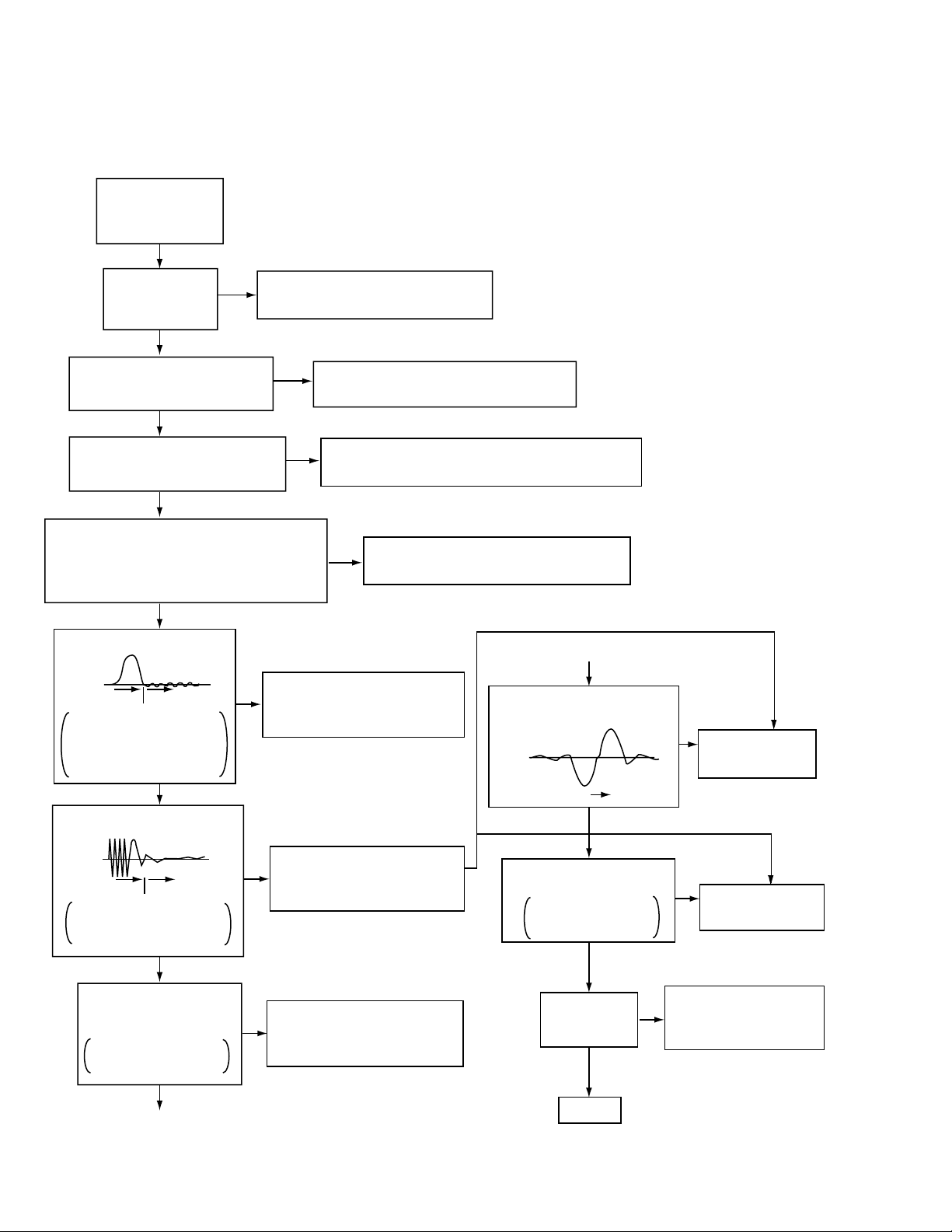
Troubleshooting
Servo volume
Press OPEN
/CLOSE key
Is tray
operation
Confirmation of tray drive circuit
N
and circuit in surrounding
correct?
Y
Is the traverse moving
along the innermost
N
perimeter for SW detection?
Y
"NO DISC" message appears
Y
immediately after vertical
movement of the pick-up lens
N
The state that DISC does not rotate continues for
several seconds, and becomes NO DISC or an
error display afterwards.
The rotation of DISC becomes high-speed and
abnormal, and becomes NO DISC or an error
display afterwards.
N
Is focus retraction OK?
FE
OFF
Even when it retracts
correctly, if it is out of focus
and makes repeated retries
with a clicking sound, it is
in error.
ON
See "(4) Focus ON error"
N
in "Check points for
individual errors"
Y
Is tracking retraction OK?
See "(3) Traverse movement error"
in "Check points for individual errors"
See "(2) Disk detection, distinction error"
in "Check points for individual errors"
Y
See "(1) Spindle startup error"
in "Check points for individual errors"
Is the inter-layer jump OK?
FE
LO LI
A
Two layers of DVD only.
N
(8) Inter-layer
jump error
Y
TE
OFF
If TE waveform reappears
or fails to converge after the
TE retraction, it is in error.
Is the spindle servo
locked correctly?
Is the RF OUT waveform
locked correctly?
1-28
A
ON
See "(5) Tracking ON error"
N
in "Check points for
individual errors"
Has the disc information
been collected?
Stop will result
N
(7) Address read
error
Y
Y
Check (9),(10),(11), and
See "(6) Spindle CLV error"
N
in "Check points for
individual errors"
Is playback
possible?
Y
N
(12) items in "Check points
for individual errors"
Y
OK !
Page 29

XV-FA90BK/XV-FA92SL/XV-FA95GD
Check points for each error
(1) Spindle start error
1.Defective spindle motor
*Are there several ohms resistance between each pin of CN201 "11-10","10-9","11-9"?
(The power supply is turned off and measured.)
*Is the sign wave of about 100mVp-p in the voltage had from each terminal?
[ CN201"6"(H1-),"7"(H1+),"4"(H2-),"5"(H2+),"2"(H3-),"3"(H3+) ]
2.Defective spindle motor driver (IC251)
*Has motor drive voltage of a sine wave or a rectangular wave gone out to each terminal(SM1~3)
of CN201"9,10,11" and IC251"2,4,7"?
*Is FG pulse output from the terminal of IC251"24"(FG) according to the rotation of the motor?
*Is it "L(about 0.9V)" while terminal of IC251"15"(VH) is rotating the motor?
3.Has the control signal come from servo IC or the microcomputer?
*Is it "L" while the terminal of IC251"18"(SBRK) is operating?
Is it "H" while the terminal of IC251"23"(/SPMUTE) is operating?
*Is the control signal input to the terminal of IC251"22"(EC)?
(changes from VHALF voltage while the motor is working.)
*Is the VHALF voltage input to the terminal of IC251"21"(ECR)?
4.Is the FG signal input to the servo IC?
*Is FG pulse input to the terminal of IC201"53"(FG) according to the rotation of the motor?
(2) Disc Detection, Distinction error (no disc, no RFENV)
<About frontend section>
* Laser is defective.
* Front End Processor is defective (IC101).
* APC circuit is defective. --- Q101,Q102.
* Pattern is defective. --- Lines for CN101 - All patterns which relate to pick-up and patterns between IC101
* Servo IC is defective (IC201).
* IC101 --- For signal from IC101 to IC201, is signal output from IC101 "20" (ASOUT) and
IC101 "41"(RFENV) and IC101 "22" (FEOUT)?
<About loading mechanism section>
* The disc exists in a sub tray. However, a sub tray is sent as follows the turntable without rising.
(Especially, when the disk is CD-RW)
--- IC81 is defective. Exchanges for "GP2S28J" of the rank specification parts.
1-29
Page 30

XV-FA90BK/XV-FA92SL/XV-FA95GD
(3) Traverse movement NG
1.Defective traverse driver
*Has the voltage come between terminal of CN101 "15" and "13" ?
2.Defective BTL driver (IC271)
*Has the motor drive voltage gone out to IC271"17" or "18"?
3.Has the control signal come from servo IC or the microcomputer?
*Is it "H" while the terminal of IC271"9"(STBY1) ?
*TRSDRV Is the signal input? (IC201 "51")
4.TRVSW is the signal input from microcomputer? (IC401 "50")
(4) Focus ON NG
* Is FE output ? --- Pattern, IC101
* Is FODRV signal sent ? (R279) --- Pattern, IC201
* Is driving voltage sent ?
IC271 "13", "14" --- If NG, pattern, driver, mechanical unit .
* Mechanical unit is defective.
(5) Tracking ON NG
* When the tracking loop cannot be drawn in, TE shape of waves does not settle.
* Mechanical unit is defective.
Because the self adjustment cannot be normally adjusted, the thing which cannot be normally
drawn in is thought.
* Periphery of driver (IC271)
Constant or IC it self is defective.
* Servo IC (IC201)
When improperly adjusted due to defective IC.
(6) Spindle CLV NG
* IC101 -- "35"(RF OUT), "30"(RF-), "31(RF+).
* Does not the input or the output of driver's spindle signal do the grip?
* Has the tracking been turned on?
* Spindle motor and driver is defective.
* Additionally, "IC101 and IC201" and "Mechanism is defective(jitter)", etc. are thought.
(7) Address read NG
* Besides, the undermentioned cause is thought though specific of the cause is difficult because various
factors are thought.
Mechanism is defective. (jitter)
IC201, IC301, IC401.
The disc is dirty or the wound has adhered.
(8) Between layers jump NG (double-layer disc only)
Mechanism defective
Defect of driver's IC(IC271)
Defect of servo control IC(IC201)
1-30
Page 31

XV-FA90BK/XV-FA92SL/XV-FA95GD
(9) Neither picture nor sound is output
1.It is not possible to search
*Has the tracking been turned on?
*To
"(5) Tracking ON NG" in "Check points for each error"
*Is the feed operation normal?
To "(3) traverse movement NG" in "Check points for each error" when it is not normal.
Are not there caught of the feeding mechanism etc?
(10) Picture is distorted or abnormal sound occurs at intervals of several seconds.
Is the feed operation normal?
Are not there caught of the feeding mechanism etc?
(11) Others
The image is sometimes blocked, and the image stops.
The image is blocked when going to outer though it is
normal in surroundings in the disk and the stopping
symptom increases.
when the tracking is not normal.
There is a possibility with bad jitter
value for such a symptom.
(12) CD During normal playback operation
a) Is TOC reading normal?
Displays total time
for CD-DA.
Shifts to double-speed
mode for V-CD.
YES
NO
b)Playback possible?
*--:-- is displayed during FL search.
According to [It is not possible to search ] for DVD(9), check the feed
and tracking systems.
*No sound is output although the time is displayed.(CA-DA)
DAC, etc, other than servo.
*The passage of time is not stable, or picture is abnormal.(V-CD)
*The wound of the disc and dirt are confirmed.
1-31
Page 32

XV-FA90BK/XV-FA92SL/XV-FA95GD
Description of major ICs
AN8702FH(IC101):Frontend processor
1.Pin layout
HDTYPE
VIN12
VIN11
GND1
VIN4
VIN3
VIN2
VIN1
VREF1
VCC1
VIN10
VIN9
VIN8
VIN7
646362616059585756555453525150
VIN6
VIN5
49
2.Pin function
Pin No.
1
2
3
4
5
6
7
8
9
10
11
12
13
14
15
16
17
18
19
20
21
22
23
24
25
26
27
28
29
30
31
32
33
Symbol
PC1
PC01
PC2
PC02
TGBAL
TBAL
FBAL
POFLT
DTRD
IDGT
STANDBY
SEN
SCK
STDI
RSEL
JLINE
TEN
TEOUT
ASN
ASOUT
FEN
FEOUT
VSS
TG
VDD
GND2
VREF2
VCC2
VHALF
DFLTON
DFLTOP
DSFLT
GND3
1
PC1
2
PC01
3
PC2
4
PC02
5
TGBAL
6
TBAL
7
FBAL
8
POFLT
9
DTRD
10
IDGT
SEN
SCK
STDI
RSEL
JLINE
11
12
13
14
15
16
171819202122232425262728293031
TEN
TEOUT
STANDBY
I/O Description
Disc detection signal input (DVD)
I
I/O
Laser current control terminal
I
Disc detection signal input (CD)
I/O
Laser current control terminal
I
Tangential phase balance control terminal
I
Tracking balance control terminal
I
Focus balance control terminal
O
Track detection threshold level terminal
I
Data slice part data read signal input terminal
(For RAM)
I
Data slice part address part gate signal input
terminal( For RAM)
I
Standby mode control terminal
I
SEN(Serial data input terminal)
I
SCK(Serial data input terminal)
I
STDI(Serial data input terminal)
I
J-line setting input(FEP)
O
Tracking error signal output terminal
O
Full adder signal output
I
Focus error output amplifier reversing input terminal
O
Focus error signal output terminal
-
Connect to GND
O
Tangential phase error signal output terminal
-
Power supply terminal 3V
-
Connect to GND
O
VREF2 voltage output terminal
-
Power supply terminal 5V
O
VHALF voltage output terminal
O
Equivalence RF-
O
Equivalence RF+
-
Connect to GND
AN8702FH
FEN
ASN
FEOUT
ASOUT
VSS
TG
VDD
Pin No.
34
35
36
37
38
39
40
41
42
43
44
45
46
47
48
49
50
51
52
53
54
55
56
57
58
59
60
61
62
63
64
48
RFINN
RFINP
47
TESTSG
46
AGCO
45
AGCG
44
PEAK
43
42
BOTTOM
41
RFENV
40
BDO
39
OFTR
38
DCRF
37
RFC
36
VCC3
35
RFOUT
34
RFDIFO
33
GND3
32
VCC2
GND2
VREF2
VHALF
DFLTON
DSFLT
DFLTOP
Symbol I/O Description
RFDIFO
To TP101
RFOUT
VCC3
-
Power supply terminal 5V
-
RFC
All addition amplifier capacitor terminal
DCRF
OFTR
BDO
RFENV
BOTTOM
PEAK
AGCG
O
OFTR output terminal
O
O
Drop out
O
RF envelope output terminal
O
Bottom envelope detection filter terminal
O
Peak envelope detection filter terminal
O
AGC amplifier gain control terminal
AGCO
TESTSG
RFINP
RFINN
VIN5
VIN6
VIN7
VIN8
VIN9
VIN10
VCC1
VREF1
VIN1
VIN2
VIN3
VIN4
GND1
VIN11
VIN12
HDTYPE
I
TEST signal input terminal
I
RF signal positive input terminal
I
RF signal negative input terminal
I
Focus input of external division into two terminal
I
Focus input of external division into two terminal
I
I
I
Focus input of external division into two terminal
I
Focus input of external division into two terminal
-
Power supply terminal 5V
O
VREF1 voltage output terminal
I
External division into four (DVD/CD) RF input
terminal1
I
External division into four (DVD/CD) RF input
terminal2
I
External division into four (DVD/CD) RF input
terminal3
I
External division into four (DVD/CD) RF input
terminal4
-
Connect to GND
I
Tracking input
I
Tracking input
-
Connect to ground
1-32
Page 33

BA5983FM-X (IC271) : 4CH DRIVER
1.Block diagram
27
26
25
28
Vcc
10k
24
20k
23 22
10k
20k
21
STAND BY
CH4
XV-FA90BK/XV-FA92SL/XV-FA95GD
20
19
Vcc
10k
10k
18
Level Shift
17 16
10k
10k
10k
10k
15
10k
10k
Level Shift
10k
Level Shift
10k
10k
Level Shift
10k
10k
10k 10k
12
10k
13
Vcc
10
10k
10k
11
STAND BY
CH1/2/3
1
2
3
5
4
6
7
89
2.Pin function
Pin No. Pin No.Symbol SymbolI/O I/OFunction Function
10
11
12
13
14
1
2
3
4
5
6
7
8
9
BIAS IN
OPIN1(+)
OPIN1(-)
OPOUT1
OPIN2(+)
OPIN2(-)
OPOUT2
GND
STBY1
PowVcc1
VO2(-)
VO2(+)
VO1(-)
VO1(+)
Input for Bias-amplifier
I
Non inverting input for CH1 OP-AMP
I
Inverting input for CH1 OP-AMP
I
Output for CH1 OP-AMP
O
Non inverting input for CH2 OP-AMP
I
Inverting input for CH2 OP-AMP
I
Output for CH2 OP-AMP
O
Substrate ground
-
Input for CH1/2/3 stand by control
I
Vcc for CH1/2 power block
-
Inverted output of CH2
O
Non inverted output of CH2
O
Inverted output of CH1
O
Non inverted output of CH1
O
15
16
17
18
19
20
21
22
23
24
25
26
27
28
VO4(+)
VO4(-)
VO3(+)
VO3(-)
PowVcc2
STBY2
GND
OPOUT3
OPIN3(-)
OPIN3(+)
OPOUT4
OPIN4(-)
OPIN4(+)
PreVcc
O
Non inverted output of CH4
O
Inverted output of CH4
O
Non inverted output of CH3
O
Inverted output of CH3
-
Vcc for CH3/4 power block
I
Input for Ch4 stand by control
-
Substrate ground
O
Output for CH3 OP-AMP
I
Inverting input for CH3 OP-AMP
I
Non inverting input for CH3 OP-AMP
O
Output for CH4 OP-AMP
I
Inverting input for CH4 OP-AMP
I
Non inverting input for CH4 OP-AMP
-
Vcc for pre block
10k
10k
14
74LCX373MTC-X(IC512,IC513)
1.Pin layout
1
OE
2
Q0
3
D0
4
D1
5
Q1
6
Q2
7
D2
8
D3
9
Q3
10
GND
20
19
18
17
16
15
14
13
12
11
2.Pin function
VCC
Q7
D7
D6
Q6
Q5
D5
D4
Q4
LE
Symbol Description
D0~D7
LE
OE
Q0~Q7
Data inputs
Latch enable input
Output enable input
3-State latch outputs
3.Truth table
INPUTS OUTPUTS
LE
X
H
H
OE
H
L
L
L
L
Dn
X
L
H
X
H = HIGH Voltage level
L = LOW Voltage level
Z = High impedance
X = Immaterial
Q0 = Previous Q0 before HIGH to LOW transition of latch enable
Qn
Z
L
H
Q0
1-33
Page 34

XV-FA90BK/XV-FA92SL/XV-FA95GD
BA6664FM-X(IC251):Spindle motor driver
1.Pin layout
1
NC
A3
NC
A2
NC
NC
A1
29
GND
H1+
10
H1-
11
H2+
12
H2-
13
H3+
14
H3-
2.Pin function
28
2
3
4
5
6
7
8
9
RNF
27
VM
26
GSW
25
VCC
24
FG
23
PS
22
EC
30
21
ECR
20
FR
19
FG2
18
SB
17
CNF
16
BR
15
VH
Pin No.
1
2
3
4
5
6
7
8
9
10
11
12
13
14
15
16
17
18
19
20
21
22
23
24
25
26
27
28
29
30
Symbol
NC
A3
NC
A2
NC
NC
A1
GND
H1+
H1-
H2+
H2-
H3+
H3-
VH
BR
CNF
SB
FG2
FR
ECR
EC
PS
FG
VCC
GSW
VM
RNF
I/O
-
O
-
O
-
-
O
I
I
I
I
I
I
I
-
-
O
-
I
I
O
O
-
O
-
O
-
-
Description
Non connect
Output 3 for spindle motor
Non connect
Output 2 for spindle motor
Non connect
Non connect
Output 1 for spindle motor
Connect to ground
Positive input for hall input AMP 1
Negative input for hall input AMP 2
Positive input for hall input AMP 2
Negative input for hall input AMP 2
Positive input for hall input AMP 3
Negative input for hall input AMP 3
Hall bias terminal
Non connect
Capacitor connection pin for phase compensation
Short brake terminal
Non connect
Non connect
Torque control standard voltage input terminal
Torque control voltage input terminal
Start/stop switch (power save terminal)
FG signal output terminal
Power supply for signal division
Gain switch
Power supply for driver division
Resistance connection pin for output current sense
Connect to ground
Connect to ground
1-34
Page 35

XV-FA90BK/XV-FA92SL/XV-FA95GD
JCV8005-3(IC500):CPPM (Content protection for pre-recorded media)
1.Pin layout
80 51
81
50
100
1 30
2.Pin function
Pin No. I/O
1
2
3~10
11
12
13~20
21
22
23
24
25
26
27
28
29
30
31
32
33~36
37
38~41
42
43
44
45
46
47
48
49
50
51
52
53
54
55
56
57
58
31
Symbol
VDD
GND
HDATA0~7
VDD
GND
HADDR0~7
VDD
GND
NCS
NRD
NWR
NIRQ
WAIT
NRESET
VDD
GND
VDD
GND
STD7~4_OUT
GND
STD3~0_OUT
VDD
GND
REQ_IN
DACK_OUT
STCLK_OUT
SYNC_OUT
STERROUT
VDD
GND
VDD
GND
G_NRD
G_NWR
G_WITODC
G_CSDEC
G_WITDEC
VDD
-
-
I/O
-
I
-
I
I
I
O
O
I
-
-
-
-
O
-
O
-
-
I
O
O
O
-
-
-
-
-
I
I
I
I
I
-
JCV8005-3 1/2
Description
Power supply
Connect to ground
Data input/output terminal (both by 8 bits)
Power supply
Connect to ground
8 bit address bus to internal address (connect to host)
Power supply
Connect to ground
Chip select signal from host
Data read signal from host
Data write signal from host
Interrupt of request to host
Wait demand to host
Reset signal from host
Power supply
Connect to ground
Power supply
Connect to ground
Data output to DVD decoder (8 bits)
Connect to ground
Data output to DVD decoder (8 bits)
Power supply
Connect to ground
Request signal for forwarding control by decoder
Output signal to decoder which shows effective data
Data strobe signal to decoder
Sector sink signal to decoder
Non connect
Power supply
Connect to ground
Power supply
Connect to ground
Glue logic input signal from host
Glue logic input signal from host
Glue logic input signal from front end
Glue logic input signal from host
Glue logic input signal from decoder
Power supply
1-35
Page 36

XV-FA90BK/XV-FA92SL/XV-FA95GD
2.Pin function
Pin No. I/O
59
60
61
62
63
64
65
66,67
68
69
70
71
72
73
74
75
76
77
78
79
80
81
82
83
84
85
86
87
88
89
90~93
94
95~98
99
100
Symbol
GND
WAIT1
WAIT2
WAITIN
VDD
GND
TEST_IN
NC
VDD
GND
CLKOCTL
NC
OSCI
OSCO
NC
VDD
GND
33OUT
169OUT
VDD
GND
VDD
GND
STERR_IN
SYNC_IN
STCLK_IN
DACK_IN
REQ_OUT
VDD
GND
STD0~3_IN
GND
STD4~7_IN
VDD
GND
JCV8005-3 2/2
Description
-
O
I
-
I
-
-
I
I
O
-
-
O
O
-
-
-
-
I
I
I
I
O
-
-
I
-
I
-
-
Connect to ground
Glue logic output signal to host
Non connect
Glue logic input signal (connect to 27 pin)
Power supply
Connect to ground
Connect to ground
Non connect
Power supply
Connect to ground
Input terminal for crystal-oscillator circuit on/off control
Non connect
Crystal oscillation terminal (input side)
Crystal oscillation terminal (output side)
Non connect
Power supply
Connect to ground
Oscillation output terminal
Oscillation output terminal
Power supply
Connect to ground
Power supply
Connect to ground
Presence of data error from front end
Sector sink signal from front end
Data clock signal from front end
Signal which shows effective data from front end
Request signal for forwarding control to front end
Power supply
Connect to ground
Data input from front end (8 bits)
Connect to ground
Data input from front end (8 bits)
Power supply
Connect to ground
1-36
Page 37

K4S643232E-TC60(IC505):DRAM
1.Block diagram
Bank select
XV-FA90BK/XV-FA92SL/XV-FA95GD
I/O control
LWE
Data input register
LDQM
refresh counter
Row buffer
Address register
CLK
Row decoder
512K x 32
512K x 32
512K x 32
512K x 32
ADD
LCBR
LRAS
Col. buffer
Column decoder
Latency & burst length
LCKE
LRAS
LCBR LWE
LCAS LWCBR
Programming register
Timing register
CLK CKE CS RAS CAS WE DQM
2.Pin function
Symbol Description Symbol Description
CLK
CS
CKE
A0~A10
BA0,1
RAS
CAS
WE
System clock signal input
Chip select input
Clock enable
Address
Bank select address
Row address strobe
Column address strobe
Write enable
DQM0~3
DQ0~31
VDD
VSS
VDDQ
VSSQ
NC
Data input/output mask
Data input/output
Power supply terminal
Connect to ground
Power supply terminal
Connect to ground
Non connect
Sense AMP
Output buffer
DQI
LDQM
1-37
Page 38

XV-FA90BK/XV-FA92SL/XV-FA95GD
MN102L25GGW1(IC401):Unit CPU
Pin function
Pin No. Pin No.
Symbol Symbol
1
2
3
4
5
6
7
8
9
10
11
12
13
14
15
16
17
18
19
20
21
22
23
24
25
26
27
28
29
30
31
32
33
34
35
36
37
38
39
40
41
42
43
44
45
46
47
48
49
50
WAIT
RE
SPMUTE
WEN
LMMUTE
CS1
CS2
CS3
DRVMUTE
SPKICK
LSIRST
WORD
A0
A1
A2
A3
VDD
SYSCLK
VSS
XI
XO
VDD
OSCI
OSCO
MODE
A4
A5
A6
A7
A8
A9
A10
A11
VDD
A12
A13
A14
A15
A16
A17
A18
A19
VSS
A20
TXSEL
HAGUP
TCLOSE
TOPEN
HMFON
TRVSW
I/O I/O
Micon wait signal input
I
Read enable
O
Spindle muting output to IC251
O
Write enable
O
Loading motor standby control
O
Chip select for ODC
O
Chip select for CPPM
O
Connect to TP312
Driver mute
O
Spin kick (Non connect)
O
LSI reset
O
Bus selection input
O
Address bus 0 for CPU
O
Address bus 1 for CPU
O
Address bus 2 for CPU
O
Address bus 3 for CPU
O
Power supply
Connect to TP169
Ground
Not use (Connect to vss)
Connect to TP170
Power supply
Clock signal input
I
Clock signal output
O
CPU Mode selection input
I
Address bus 4 for CPU
O
Address bus 5 for CPU
O
Address bus 6 for CPU
O
Address bus 7 for CPU
O
Address bus 8 for CPU
O
Address bus 9 for CPU
O
Address bus 10 for CPU
O
Address bus 11 for CPU
O
Power supply
Address bus 12 for CPU
O
Address bus 13 for CPU
O
Address bus 14 for CPU
O
Address bus 15 for CPU
O
Address bus 16 for CPU
O
Address bus 17 for CPU
O
Connect to TP913
Connect to TP912
Ground
Connect to TP911
Connect to TP910
-
O
Connect to TP311
Connect to TP310
-
Detection switch of traverse
I
inside
Function
51
52
53
54
55
56
57
58
59
60
61
62
63
64
65
66
67
68
69
70
71
72
73
74
75
76
77
78
79
80
81
82
83
84
85
86
87
88
89
90
91
92
93
94
95
96
97
98
99
100
SWUPDN
SWOPEN
ADSCEN
VDD
FEPEN
SLEEP
BUSY
REQ
CIRCEN
-
VSS
EPCS
EPSK
DPDI
EPDO
VDD
SCLKO
S2UDT
U2SDT
CPSCK
SDIN
SDOUT
-
-
NMI
ADSCIRQ
ODCIRQ
DECIRQ
CSSIRQ
ODCIRQ2
ADSEP
RST
VDD
TEST1
TEST2
TEST3
TEST4
TEST5
TEST6
TEST7
TEST8
VSS
D0
D1
D2
D3
D4
D5
D6
D7
Function
Elevator UP/DOWN switch detect
I
Tray OPEN/CLOSE switch detect
I
Serial enable signal for ADSC
O
Power supply
Serial enable signal for FEP
O
Standby signal for FEP
O
Non connect
Communication Request
O
CIRC command select
O
Connect to TP308
Ground
EEPROM chip select
O
EEPROM clock
O
EEPROM data input
I
EEPROM data output
O
Power supply
Communication clock
I
Communication input data
I
Communication output data
O
Clock for ADSC serial
O
ADSC serial data input
I
ADSC serial data output
O
Not use
Not use
Not use
Interrupt input of ADSC
I
Interrupt input of ODC
I
Interrupt input of ZIVA
I
Not use
Interruption of system control
I
Address data selection input
I
Reset input
I
Power supply
Test signal 1 input
I
Test signal 2 input
I
Test signal 3 input
I
Test signal 4 input
I
Test signal 5 input
I
Test signal 6 input
I
Test signal 7 input
I
Test signal 8 input
I
Ground
Data bus 0 of CPU
I/O
Data bus 1 of CPU
I/O
Data bus 2 of CPU
I/O
Data bus 3 of CPU
I/O
Data bus 4 of CPU
I/O
Data bus 5 of CPU
I/O
Data bus 6 of CPU
I/O
Data bus 7 of CPU
I/O
1-38
Page 39

MN103S13BDA(IC301):Optical disc controller
1.Pin layout
DMARQ
NIOWR
VSS
NIORD
IORDY
NDMACK
VDD
INTRQ
NIOCS16
DA1
VSS
NPDIAG
DA0
DA2
VDD
NCS1FX
144
143
142
141
140
139
138
137
136
135
134
133
132
131
130
HDD15
HDD0
HDD14
VDD
HDD1
HDD13
HDD2
VSS
HDD12
VDD
HDD3
HDD11
HDD4
HDD10
VDD
HDD5
HDD9
VSS
HDD6
HDD8
HDD7
VDDH
NRESET
MASTER
NINT0
NINT1
WAITDOC
NMRST
DASPST
VDD
OSCO2
OSCI2
UATASEL
VSS
PVSSDRAM
PVDDDRAM
1
2
3
4
5
6
7
8
9
10
11
12
13
14
15
16
17
18
19
20
21
22
23
24
25
26
27
28
29
30
31
32
33
34
35
36
3738394041424344454647484950515253545556575859606162636465666768697071
129
MN103S13BDA
NCS3FX
NDASP
NTRYCL
128
127
126
VDD
NEJECT
125
124
VSS
123
MONI0
MONI1
122
121
MONI2
MONI3
120
119
SDATA
SCLOCK
118
117
XV-FA90BK/XV-FA92SL/XV-FA95GD
VDD
DAT0
DAT1
DAT2
DAT3
CHCK40
NCLDCK
SUBC
116
115
114
113
112
111
110
109
108
SBCK
107
VSS
106
P0
105
P1
104
PVDD
103
PVSS
102
VDD
101
OSCO1
100
OSCI1
99
VSS
98
LRCK
97
BLKCK
96
IPFLAG
95
DACCLK
94
DACLRCK
93
DA C DATA
92
NTRON
91
LG
90
JMPINH
89
IDHOLD
88
SBCK/PLLOK
87
CLKOUT2
86
VDD
85
NRST
84
MMOD
83
VSS
82
CPDET1
81
CPDET2
80
BDO
79
IDGT
78
DTRD
77
TEHLD
76
VDD
75
CLKOUT1
74
CPUDT0
73
CPUDT1
72
2.Block diagram
DVD-ROM
Formatter
CGEN
MODE
CPUADR17
CPUADR16
VSS
CPUADR15
CPUADR14
CPUADR13
CD-PRE
Instruction
memory
(40KB)
DATA
MEMORY
(6KB)
VDD
CPUADR9
CPUADR8
CPUADR11
CPUADR10
CPUADR7
CPUADR12
Formatter
General purpose IO bus
CPUADR6
CPUADR5
CPUADR4
CPUADR3
CPUADR2
i /t
High speed IO bus
32 bit
CPU core
GCAL
CPUADR1
VSS
CPUADR0
NCS
NWR
ECC
NRD
VDD
CPUDT7
CPUDT6
PVPPDRAM
CPUDT5
PVSSDRAM
PVDDDRAM
PTESTDRAM
Host i / f
MPEG i / t
DMA
BCU
DRAMC
VSS
CPUDT4
CPUDT3
CPUDT2
ATAPI
4Mbit
DRAM
WDT
16 bit
timer x 2
SYSTEM
i / f
INTC
1-39
Page 40

XV-FA90BK/XV-FA92SL/XV-FA95GD
3.Pin function (1/3)
Pin No.
1
2
3
4
5
6
7
8
9
10
11
12
13
14
15
16
17
18
19
20
21
22
23
24
25
26
27
28
29
30
31
32
33
34
35
36
37
38
39
40
41
42
43
44
45
46
47
48
49
50
Symbol
HDD15
HDD0
HDD14
VDD
HDD1
HDD13
HDD2
VSS
HDD12
VDD
HDD3
HDD11
HDD4
HDD10
VDD
HDD5
HDD9
VSS
HDD6
HDD8
HDD7
VDDH
NRESET
MASTER
NINT0
NINT1
WAITDOC
NMRST
DASPST
VDD
OSCO2
OSCI2
UATASEL
VSS
PVSSDRAM
PVDDDRAM
CPUADR17
CPUADR16
VSS
CPUADR15
CPUADR14
CPUADR13
CPUADR12
VDD
CPUADR11
CPUADR10
CPUADR9
CPUADR8
CPUADR7
CPUADR6
I/O
I/O
I/O
I/O
I/O
I/O
I/O
I/O
I/O
I/O
I/O
I/O
I/O
I/O
I/O
I/O
I/O
I
I/O
O
O
O
O
I
-
O
I
I
-
I
I
-
I
I
I
I
-
I
I
I
I
I
I
Description
ATAPI Data
ATAPI Data
ATAPI Data
Power supply 3V
ATAPI Data
ATAPI Data
ATAPI Data
Connect to GND
ATAPI Data
Power supply 2.7V
ATAPI Data
ATAPI Data
ATAPI Data
ATAPI Data
Power supply 3V
ATAPI Data
ATAPI Data
Connect to GND
ATAPI Data
ATAPI Data
ATAPI Data
ATAPI Reset input
ATAPI Master/slave select
Interruption of system control 0
Interruption of system control 1
Wait control of system control
Reset of system control (Connect to TP302)
Setting of initial value of DASP signal
Power supply 3V
Non connect
Non connect
Connect to VSS
Connect to GND
Connect to VSS
Connect to VDD(2.7V)
System control address
System control address
Connect to GND
System control address
System control address
System control address
System control address
Power supply 2.7V
System control address
System control address
System control address
System control address
System control address
System control address
1-40
Page 41

3.Pin function (2/3)
XV-FA90BK/XV-FA92SL/XV-FA95GD
Pin No.
51
52
53
54
55
56
57
58
59
60
61
62
63
64
65
66
67
68
69
70
71
72
73
74
75
76
77
78
79
80
81
82
83
84
85
86
87
88
89
90
91
92
93
94
95
96
97
98
99
100
Symbol
CPUADR5
CPUADR4
CPUADR3
CPUADR2
CPUADR1
VSS
CPUADR0
NCS
NWR
NRD
VDD
CPUDT7
CPUDT6
PVPPDRAM
PTESTDRAM
PVDDDRAM
PVSSDRAM
CPUDT5
CPUDT4
CPUDT3
VSS
CPUDT2
CPUDT1
CPUDT0
CLKOUT1
VDD
TEHLD
DTRD
IDGT
BDO
CPDET2
CPDET1
VSS
MMOD
NRST
VDD
CLKOUT2
SBCK/PLLOK
IDOHOLD
JMPINH
LG
NTRON
DAC DATA
DACLRCK
DACCLK
IPFLAG
BLKCK
LRCK
VSS
OSCI1
I/O
I/O
I/O
O
I/O
I/O
I/O
I/O
I/O
I/O
O
O
O
O
O
O
O
O
O
O
O
Description
System control address
I
System control address
I
System control address
I
System control address
I
System control address
I
Connect to GND
System control address
I
System control chip select
I
Writing system control
I
Reading system control
I
Power supply 3V
System control data
System control data
Connect to VSS
Connect to VSS
I
Connect to VDD(2.7V)
Connect to VSS
System control data
System control data
System control data
Connect to GND
System control data
System control data
System control data
Clock signal output (16.9/11.2/8.45MHz)
Power supply 3V
Mirror gate (Connect to TP141)
Data frequency control switch (Connect to TP304)
CAPA switch
RF Dropout/BCA data
I
Outer capacity detection
I
Inner capacity detection
I
Connect to GND
Connect to VSS
I
System reset
I
Power supply 3V
Clock 16.9MHz
Flame mark detection
ID gate for tracking holding
Jump prohibition
Land/group switch
Tracking ON
I
Serial data output (Connect to TP148)
Identification signal of L and R (Connect to TP149)
Clock for serial data output
I
Input of IP flag
I
Sub code/block/input clock
I
Identification signal of L and R (Connect to VSS)
I
Connect to GND
Oscillation input terminal 16.9MHz
I
1-41
Page 42

XV-FA90BK/XV-FA92SL/XV-FA95GD
3.Pin function (3/3)
Pin No.
101
102
103
104
105
106
107
108
109
110
111
112
113
114
115
116
117
118
119
120
121
122
123
124
125
126
127
128
129
130
131
132
133
134
135
136
137
138
139
140
141
142
143
144
Symbol
OSCO1
VDD
PVSS
PVDD
P1
P0
VSS
SBCK
SUBC
NCLDCK
CHCK40
DAT3
DAT2
DAT1
DAT0
VDD
SCLOCK
S DATA
MONI3
MONI2
MONI1
MONI0
VSS
NEJECT
VDD
NTRYCL
NDASP
NCS3FX
NCS1FX
VDD
DA2
DA0
NPDIAG
VSS
DA1
NIOCS16
INTRQ
VDD
NDMACK
IORDY
NIORD
VSS
NIOWR
DMARQ
I/O
O
-
-
I/O
I/O
-
O
I
I
I
I
I
I
I
I/O
I/O
O
O
O
O
-
I
-
I
I/O
I
I
I/O
I/O
I/O
I/O
O
O
-
I
O
I
I/O
O
Description
Oscillation output terminal 16.9MHz
Power supply 3V
Connect to GND
Power supply 3V
Terminal master polarity switch input
CIRC-RAM,OVER/UNDER Interruption
Connect to GND
Clock output for sub code,serial input
Sub code,serial input
Sub code,flame clock input
Clock is read to DAT3~0 (Output of division frequency from ADSC)
Data is read from disc (Going side by side output from ADSC)
Data is read from disc (Going side by side output from ADSC)
Data is read from disc (Going side by side output from ADSC)
Data is read from disc (Going side by side output from ADSC)
Power supply 3V
Debug serial clock (270 ohm pull up)
Debug serial data (270 ohm pull up)
Internal good title monitor (Connect to TP150)
Internal good title monitor (Connect to TP151)
Internal good title monitor (Connect to TP152)
Internal good title monitor (Connect to TP153)
Connect to GND
Eject detection
Power supply 2.7V
Non connect (Tray close detection)
ATAPI drive active / slave connect I/O
Non connect (ATAPI host chip select)
Non connect (ATAPI host chip select)
Power supply 3V
ATAPI host address
Non connect (ATAPI host address)
ATAPI Slave master diagnosis input
Connect to GND
Non connect (ATAPI host address)
Output of selection of width of ATAPI host data bus
ATAPI Host interruption output
Power supply 3V
Non connect (ATAPI Host DMA characteristic)
ATAPI Host ready output (Connect to TP157)
Non connect (ATAPI host read)
Connect to GND
ATAPI Host write
ATAPI Host DMA request (Connect to TP159)
1-42
Page 43

MN67706ZY (IC201) : Auto digital servo controller
1.Pin layout
33VDD
33VSS
TEST
MINTEST
NCLDCK/JUMP
SUBC
IPFLAG
DACCLK
NTRON
DACDATA/LG
DACLRCK/JMPINH
IDHOLD
SBCK/PLLOK
BLKCK/CPDET1
LRCK/CPDET2
IDGT/TEMUTE
DTRD
25VDD
25VSS
TILTN
75747372717069686766656463626160595857565554535251
CHCK40
DAT3
DAT2
DAT1
DAT0
33VSS
33VDD
XRESET
ENS
ENC
CPUIRQ
CPUCLK
CPUDTIN
CPUDTOUT
MONA
MONB
MONC
25VSS
25VDD
LDCUR(AD6)
TDOFS(AD5)
TG(AD4)
RFENV(AD3)
NC
TX
76
77
78
79
80
81
82
83
84
85
86
87
88
89
90
91
92
93
94
95
96
97
98
99
100
123456789
MN67706ZY
101112131415161718192021222324
TILT
TILTPFGSPDRV
XV-FA90BK/XV-FA92SL/XV-FA95GD
TRSDRV
TSTSG
50
BDO
49
SYSCLK
48
OFTR
47
33VDD
46
33VSS
45
FBAL
44
TBAL
43
TGBAL
42
AVSS
41
ROUT
40
LOUT
39
AVDD
38
JLINE
37
DBALO
36
VCOF
35
TRCRS
34
CMPIN
33
LPFOUT
32
LPFIN
31
AVSS
30
HPFOUT
29
HPFIN
28
AVDD
27
VFOSHORT
26
25
TE(AD1)
FE(AD0)
AS(AD2)
AVSS
AVDD
TRDRV(DA0)
FODRV(DA1)
ARF
NARF
IREF1
IREF2
DSLF1
AVDD
DSLF2
PLPG
VHALF
PLFG
VREFH
2.Pin functions (1/3)
Pin No. Symbol I/O Description
I
AS : Full adder signal(FEP)
I
Phase difference/3 beam tracking error(FEP)
I
Focus error(FEP)
-
Apply 3.3V(For analog circuit)
Focus drive(DRVIC)
Tracking drive(DRVIC)
-
Ground(For analog circuit)
I
Equivalence RF+(FEP)
I
Equivalence RF-(FEP)
I
Reference current1(For DBAL)
I
Reference current2(For DBAL)
Connect to capacitor1 for DSL
Connect to capacitor2 for DSL
-
Apply 3.3V(For analog circuit)
I
Reference voltage 1.65+-0.1V(FEP)
-
Not use(PLL phase gain setting resistor terminal)
-
Not use(PLL frequency gain setting resistor terminal)
I
Reference voltage 2.2V+-0.1V(FEP)
Connect to resistor for VREFH reference current source
-
Ground(For analog circuit)
Connect to capacitor1 for PLL
Connect to capacitor2 for PLL
Output for jitter signal monitor
I
Not use
Pull-up to VHALF
10
11
12
13
14
15
16
17
18
19
20
21
22
23
24
25
1
2
3
4
5
6
7
8
9
AS(AD2)
TE(AD1)
FE(AD0)
AVD D
FODRV(DA1)
TRDRV(DA0)
AVSS
ARF
NARF
IREF1
IREF2
DSLF1
DSLF2
AVD D
VHALF
PLPG
PLFG
VREFH
RVI
AVSS
PLFLT1
PLFLT2
JITOUT
RFDIF
CSLFL1
O
O
I/O
I/O
I/O
O
O
I/O
I/O
RVI
AVSS
PLFLT1
JITOUT
PLFLT2
RFDIF
CSLFL1
MN67706ZY
1-43
Page 44

XV-FA90BK/XV-FA92SL/XV-FA95GD
2.Pin function (2/3)
Pin No. Symbol I/O Description
26
27
28
29
30
31
32
33
34
35
36
37
38
39
40
41
42
43
44
45
46
47
48
49
50
51
52
53
54
55
56
57
58
59
60
61
62
63
64
65
66
67
68
69
70
71
72
73
74
75
76
77
78
79
80
VFOSHORT
AVDD
HPFIN
HPFOUT
AVSS
LPFIN
LPFOUT
CMPIN
TRCRS
VCOF
DBALO
JLINE
AVDD
LOUT
ROUT
AVSS
TGBAL
TBAL
FBAL
33VSS
33VDD
OFTR
SYSCLK
BDO
TSTSG
TRSDRV
SPDRV
FG
TILTP
TILT
TILTN
25VSS
25VDD
DTRD
IDGT/TEMUTE
LRCK/CPDET2
BLKCK/CPDET1
SBCK/PLLOK
IDHOLD
DACLRCK/JMPINH
DACDATA/LG
NTRON
DACCLK
IPFLAG
SUBC
NCLDCK/JUMP
MINTEST
TEST
33VSS
33VDD
CHCK40
DAT3
DAT2
DAT1
DAT0
O
I
O
I
O
I
I
I/O
O
O
O
O
O
O
O
-
-
I
I
I
O
O
O
I
O
O
O
-
-
I
I
O
O
I
I
I
I
O
O
O
O
O
I
I
-
O
O
O
O
O
VFO short output
Apply 3.3V(For analog circuit)
Pull-up to VHALF
Connect to TP208
Ground(For analog circuit)
Pull-up to VHALF
Not use
Connect to TP210
Input signal for track cross formation
JFVCO control voltage
DSL balance adjust output
J-line setting output(FEP)
Apply 3.3V(For analog circuit)
Connect to TP203 (Analog audio left output)
Connect to TP204 (Analog audio right output)
Ground(For analog circuit)
Tangential balance adjust(FEP)
Tracking balance adjust(FEP)
Focus balance adjust(FEP)
Ground(For I/O)
Apply 3.3V(For I/O)
Off track signal
16.9344MHz system clock input(ODC)
Drop out(FEP)
Calibration signal(FEP)
Traverse drive(DRVIC)
Spindle drive output(DRVIC)
FG signal input (Spindle motor driver)
Connect to TP205
Connect to TP206
Connect to TP207
Ground(For internal core)
Apply 2.5V(For internal core)
Data read control signal(ODC)
Pull-down to Ground
LR channel data strobe(ODC)/
CD sub code synchronous signal(ODC)/
CD sub code data shift clock(ODC)/PLL pull-in OK signal input
Pull-down to Ground
1bit DAC-LR channel data strobe(ODC)/
CD 1bit DAC channel data(ODC)
L : Tracking ON(ODC)
1bit DAC channel data shift clock(ODC)
CIRC error flag(ODC)
CD sub code(ODC)
CD sub code data frame clock(ODC)/DVD JUMP signal(ODC)
Pull-down to Ground(For MINTEST)
Pull-down to Ground(For TEST)
Ground(For I/O)
Apply 3.3V(For I/O)
Clock for SRDATA(ODC)
SRDATA3(ODC)
SRDATA2(ODC)
SRDATA1(ODC)
SRDATA0(ODC)
MN67706ZY
1-44
Page 45

XV-FA90BK/XV-FA92SL/XV-FA95GD
2.Pin function (3/3)
Pin No. Symbol I/O Description
81
82
83
84
85
86
87
88
89
90
91
92
93
94
95
96
97
98
99
100
33VSS
33VDD
TX
XRESET
ENS
ENC
CPUIRQ
CPUCLK
CPUDTIN
CPUDTOUT
MONA
MONB
MONC
NC
25VSS
25VDD
LDCUR(AD6)
TDOFS(AD5)
TG(AD4)
RFENV(AD3)
-
-
O
I
I
I
O
I
I
O
O
O
O
O
-
I
I
I
I
Ground(For I/O)
Apply 3.3V(For I/O)
Digital audio interface
Reset input (System control)
Servo DSC serial I/F chip select (System control)
CIRC serial I/F chip select (System control)
Interrupt request (System control)
Serial I/F clock (System control)
Serial I/F data input (System control)
Serial I/F data output (System control)
Connect to TP226 (Monitor terminal A)
Connect to TP225 (Monitor terminal A)
Connect to TP224 (Monitor terminal A)
Connect to TP211
Ground(For internal core)
Apply 2.5V(For internal core)
Laser current control terminal
Connect to TP215
Tangential phase difference(FEP)
RF envelope input(FEP)
MN67706ZY
1-45
Page 46

XV-FA90BK/XV-FA92SL/XV-FA95GD
NDV8601VWA-BB(IC501):AV Decoder
1.Pin layout
240 181
1
180
60
61 120
2.Block diagram
digital audio
serial
peripherals
DVD data
3.Pin function (1/4)
Pin No.
1
2,3
4
5
6
7~9
10
11
12,13
14
15,16
17
18
19
20,21
22
23
24
25,26
27
28
29
Symbol
VDDio
MD10,11
VDD
MD12
VSSio
MD13~15
VDDio
DQM1
MA9,8
VSSio
MA7,6
VSS
MA5
VDDio
MA4,3
MCLK
VSSio
CKE
MA2,1
VDDio
MA0
MA10
121
audio DAC
Serial
port
controller
I/O
-
I/O
-
I/O
-
I/O
O
O
O
O
O
O
O
O
O
O
digital audio
Audio
output
processor
DVD,A/V
port
+
CSS
Audio
DSP
Demux
engine
Power supply terminal 3.3V
SDRAM Data bus terminal
Power supply terminal 1.8V
SDRAM Data bus terminal
Connect to ground
SDRAM Data bus terminal
Power supply terminal 3.3V
SDRAM Data byte enable
SDRAM Address bus terminal
Connect to ground
SDRAM Address bus terminal
Connect to ground
SDRAM Address bus terminal
Power supply terminal 3.3V
SDRAM Address bus terminal
SDRAM Clock output
Connect to ground
SDRAM Clock enable output
SDRAM Address bus terminal
Power supply terminal 3.3V
SDRAM Address bus terminal
SDRAM Address bus terminal
MPEG
Video
decoder
SDRAM
controller
SDRAM
Description
Video I/O port
Video
output
processor
RISC
uProcessor
+ cache
NTSC
PA L
SCART
encoder
XBUS
controller
Video
XBUS
1-46
Page 47

3.Pin function (NDV8601VWA-BB 2/4)
XV-FA90BK/XV-FA92SL/XV-FA95GD
Pin No.
30
31
32,33
34
35
36
37
38
39
40
41
42
43
44
45,46
47
48
49
50~52
53
54~56
57
58~61
62
63,64
65
66
67
68
69
70
71
72
73
74
75
76
77
78
79
80
81
82
83
84
85
86
87
88
89
90
Symbol
MA11
VSSio
MA12,13
VDD
CS0
VDDio
RAS
CAS
WE
VSSio
DQM0
DQM2
MD16
VDDio
MD17,18
VSS
MD19
VSSio
MD20~22
VDDio
MD23~25
VSSio
MD26~29
VDDio
MD30,31
DQM3
CS1
VSSD
SPDIF
VSSio
AIN
AOUT3
AOUT2
AOUT1
AOUT0
VDDio
PCMCLK
VDD
ACLK
LRCLK
SRST
RSTP
VSSio
RXD1
SSPIN1
VSS
SSPOUT1
SSPCLK1
SSPCLK0
VDD
SSPIN0
I/O
Non connect
Connect to ground
SDRAM Address bus, reserved for terminal compatibility with 64Mb SDRAM
O
Power supply terminal 1.8V
SDRAM Primary bank chip select
O
Power supply terminal 3.3V
SDRAM Command bit
O
SDRAM Command bit
O
SDRAM Command bit
O
Connect to ground
SDRAM Data byte enable
O
SDRAM Data byte enable
O
SDRAM Data bus terminal
I/O
Power supply terminal 3.3V
SDRAM Data bus terminal
I/O
Connect to ground
SDRAM Data bus terminal
I/O
Connect to ground
SDRAM Data bus terminal
I/O
Power supply terminal 3.3V
SDRAM Data bus terminal
I/O
Connect to ground
SDRAM Data bus terminal
I/O
Power supply terminal 3.3V
SDRAM Data bus terminal
I/O
SDRAM Data byte enable
O
SDRAM Extension bank chip select
O
Connect to ground
S/PDIF Digital audio output terminal
O
Connect to ground
Digital audio input for digital micro; can be used as GPIO
I
Serial audio output data to audio DAC for left and right channels for down-mix
O
Serial audio output data to audio DAC for surround left and right channels
O
Serial audio output data to audio DAC for center and LFE channels
O
Serial audio output data to audio DAC for left and right channels
O
Power supply terminal 3.3V
Audio DAC PCM sampling clock frequency, common clock for DACs and ADC
O
Power supply terminal 1.8V
Audio interface serial data clock, common clock for DACs and AD converter
O
Left / right channel clock, common clock for DACs and ADC
O
Active low RESET signal for peripheral reset
O
RESET_Power : from system, used to reset frequency synthesizer and rest
I
Description
of chip
Connect to ground
UART1 Serial data input from external serial device, used for IR receiver
I
SSP1 Data in or 16X clock for USART function in UART1
I/O
Connect to ground
SSP1 Data out or UART1 data-terminal-ready signal
I/O
SSP1 Clock or UART1 clear-to -send signal
I/O
SSP0 Clock or request-to-send function in UART1
I/O
Power supply terminal 1.8V
SSP0 Data in or 16X clock for USART function in UART0
I/O
1-47
Page 48

XV-FA90BK/XV-FA92SL/XV-FA95GD
3.Pin function (NDV8601VWA-BB 3/4)
1-48
Pin No.
91
92
93
94
95
96
97
98
99
100
101
102
103
104
105
106
107
108
109
110
111
112
113
114
115
116
117
118
119
120
121
122
123
124
125
126~131
132
133,134
135
136~139
140
141~144
145
146
147
148~153
154
155
156
157,158
159
Symbol
VDDio
SSPOUT0
TXD0
RXD0
CTS0
RTS0
VSSio
CXI
CXO
OSCVSS
OSCVDD
MVCKVDD
SCEN
MVCKVSS
ACLKVSS
SCMD
ACLKVDD
VDDDAK
VSSDAC
Cr/R
IOM
C/Cb/B
VAA3
Y/G
VSSA
VREF
VAA
CVBS/C
RSET
COMP
VSS
VCLK
VSYNC
HSYNC
VDDio
VI07~02
VSSio
VI01,00
VDD
AD31~28
VDDio
AD27~24
PWE3
AD23
VSSio
AD22~17
VDDio
AD16
PWE2
AD15,14
VDD
I/O
Power supply terminal 3.3V
SSP0 Data out or UART0 data-terminal-ready signal
I/O
UART0 Serial data output to an external serial device
I/O
UART0 Serial data input from external serial device
I
UART0 Clear-to-send signal
I/O
UART0 Request-to-send signal
I/O
Connect to ground
Crystal input terminal for on-chip oscillator or system input clock
I
Crystal output terminal for on-chip oscillator
O
Connect to ground for oscillator
Power supply terminal for oscillator 1.8V
Power supply terminal for main and video clock PLL 3.3V
Scan chain test enable
I
Connect to ground for main and video clock PLL
Connect to ground for audio clock PLL
Scan chain test mode
I
Power supply terminal for audio clock PLL 3.3V
Power supply terminal for DAC digital 1.8V
Connect to ground for DAC digital
Video signal output (Cr output : composite/component Red output)
O
Cascaded DAC differential output used to dump current into external resistor
O
for power
Video signal output (Chrominance output for NTSC/PAL S-Video
O
Cb output for component Blue output)
Power supply terminal for DAC analog 3.3V
Video signal output (Luminance for S-Video and component Green output)
O
Connect to ground for DAC analog
Non connect
-
Video signal output (Composite video Chrominance output for S-Video)
O
Current setting resistor of output DACs
O
Compensation capacitor connection
O
Connect to ground
Non connect
Non connect
Non connect
Power supply terminal 3.3V
Non connect
Connect to ground
Non connect
Power supply terminal 1.8V
Multiplexed address / data bus terminal
I/O
Power supply terminal
Multiplexed address / data bus terminal
I/O
Byte write enable for FLASH,EEPROM,SRAM or peripherals terminal
I/O
Multiplexed address / data bus terminal
I/O
Connect to ground
Multiplexed address / data bus terminal
I/O
Power supply terminal 3.3V
Multiplexed address / data bus terminal
I/O
Byte write enable for FLASH,EEPROM,SRAM or peripherals terminal
I/O
Multiplexed address / data bus terminal
I/O
Power supply terminal 1.8V
-
Description
Page 49

3.Pin function (NDV8601VWA-BB 4/4)
XV-FA90BK/XV-FA92SL/XV-FA95GD
Pin No.
160
161
162
163~168
169
170
171
172~176
177
178~180
181
182
183
184~187
188
189
190
191
192
193
194,195
196
197~200
201
202,203
204
205
206~209
210
211
212
213
214
215
216
217
218
219~223
224
225,226
227
228
229
230
231,232
233
234~236
237
238~240
Symbol
SCLK
ACK
VSSio
AD13~8
VDDio
PWE1
VSS
AD7~3
VSSio
AD2~0
VDDio
PWE0
ALE
LA0~3
VSSio
RD
LHLDA
LHLD
VDD
PCS0
XI01,02
VDDio
XI03~06
VSS
XI07,08
VSSio
XI09
XID10~13
VDDio
XID14
VDD
DSYNC
DREQ
DCLK
DSTB
DVD0
VSSio
DVD1~5
VDDio
DVD6,7
MD0
VSSio
MD1
VSS
MD2,3
VDDio
MD4~6
VSSio
MD7~9
I/O
External bus clock used for programmable host peripherals
O
Programmable WAIT/ACK/RDY control
I/O
Connect to ground
Multiplexed address / data bus terminal
I/O
Power supply terminal 3.3V
Byte write enable for FLASH,EEPROM,SRAM or peripherals terminal
I/O
Connect to ground
Multiplexed address / data bus terminal
I/O
Connect to ground
Multiplexed address / data bus terminal
I/O
Power supply terminal 3.3V
Byte write enable for FLASH,EEPROM,SRAM or peripherals terminal
I/O
Address latch enable
I/O
Latched address 0~3
I/O
Connect to ground
Read terminal
I/O
Bus hold acknowledge in slave mode
O
Bus hold request from external master in slave mode
I
Power supply terminal 1.8V
Peripheral chip select 0, generally used for enabling the program store
O
ROM/FLASH
Programmable general purpose external input/output
I/O
Power supply terminal 3.3V
Programmable general purpose external input/output
I/O
Connect to ground
Programmable general purpose external input/output
I/O
Connect to ground
Programmable general purpose external input/output
I/O
Programmable general purpose external input/output
I/O
Power supply terminal 3.3V
Programmable general purpose external input/output
I/O
Power supply terminal 1.8V
DVD Parallel mode sector sync
I
DVD Parallel mode data request
O
Data sampling clock
I
Parallel mode data valid, serial mode left/right clock
I
DVD Drive parallel data port
I
Connect to ground
DVD Drive parallel data port
I
Power supply terminal 3.3V
DVD Drive parallel data port
I
SDRAM Data bus terminal
I/O
Connect to ground
SDRAM Data bus terminal
I/O
Connect to ground
SDRAM Data bus terminal
I/O
Power supply terminal 3.3V
SDRAM Data bus terminal
I/O
Connect to ground
SDRAM Data bus terminal
I/O
Description
1-49
Page 50

XV-FA90BK/XV-FA92SL/XV-FA95GD
NJU3715G-W(IC802) : L.E.D.Driver
1.Pin layout
D3
1
22
21
20
19
18
17
16
15
14
13
12
VCC
D2
D1
DCH
MUTE
READY
CLR
STB
CLK
DATA
VSS
STLED
PONLED
PROGLED
DDPLED
ALED
2.Block diagram
D4
D5
D6
D7
2
3
4
5
6
7
8
9
10
11
DATA
CLK
STB
CLR
3.Pin function
Shift
resistor
Control Circuit
Latch
circuit
P1
P2
P3
P4
P5
P15
P16
1-50
PIN No.
1~5
6
7~11
12
13
14
15
16
17
18
19~21
22
I/O FunctionSymbol
O
-
O
STLED,PONLED,PROGLED
D3~D7
VSS
DDPLED,ALED
I
I
I
I
I
DATA
CLK
ST
CLR
READY
I
O
-
MUTE
DCH,D1,D2
VCC
Parallel conversion data output terminal.
Connect to GND.
Parallel conversion data output terminal.
Serial data input terminal.
Clock signal input terminal.
Strobe signal input terminal.
Clear signal input terminal.
Ready signal input.
Non connect.
Muting signal input.
Parallel conversion data output terminal.
Power supply terminal.
Page 51

SST39VF160-7CEK (IC509) : 16M EEPROM
1. Pin layout
XV-FA90BK/XV-FA92SL/XV-FA95GD
1
A15
2
A14
3
A13
4
A12
5
A11
6
A10
7
A9
8
A8
9
A19
10
NC
11
/WE
12
/RST
13
NC
14
NC
15
R/B
16
A18
17
A17
18
A7
19
A6
20
A5
21
A4
22
A3
23
A2
24
A1
2. Block diagram
A19~A0
48
A16
47
/BYTE
46
Vss
45
D15
44
D7
43
D14
42
D6
41
D13
40
D5
39
D12
38
D4
37
VDD
36
D11
35
D3
34
D10
33
D2
32
D9
31
D1
30
D8
29
D0
28
/OE
27
Vss
26
/CE
25
A0
Address Buffer & Latches
X-Decoder
16,777,216Bit
EEPROM
Cell Array
Y-Decoder
/CE
/OE
/WE
3. Pin function
Symbol FunctionPin name
A19~A0
DQ15~DQ0
/CE
/OE
/WE
VDD
Vss
NC
Address Inputs
Data Input/Output
Chip Enable
Output Enable
Write Enable
Power Supply
Ground
No Connection
Control Logic
I/O Buffers & Data Latches
DQ15~DQ0
To provide memory addresses. During sector erase A19~A11 address
lines will select the sector. During block erase A19~A15 address lines
will select the block.
To output data during read cycles and receive input data during write
cycles. Data is internally latched during a write cycle. The outputs are
in tri-state when /OE or /CE is high.
To activate the device when /CE is low.
To gate the data output buffers.
To control the write operations.
To provide 3-volt supply ( 2.7V-3.6V ).
1-51
Page 52

XV-FA90BK/XV-FA92SL/XV-FA95GD
UPD780232GC-055(IC801):System controller
1.Pin layout
60 41
61
40
80
1 20
2.Pin function
Pin No.
1
2
3,4
5
6
7
8
9
10
11
12
13
14
15
16
17
18
19
20
21
22
23
24
25
26
27
28
29
30
31
32
33
34
35
36
37
38
39~58
59
60
61~64
65~67
68~80
21
Symbol
VDD1
VSS1
X1,X2
IC(VPP)
RESET
SSPCLK1B
SSPOUT1B
SSPIN1A
POWERSW
AVCO
RINT
P.ON
CPU RESET
AVCI
FLCS
REMO
AVSS
KEY3
KEY2
CAMSW
MUDSW
VSS0
AVDD
VDD0
DATA
CLK
STB
RR
LR
LDOWN
LUP
T.IN
T.OUT
EXIN
PD
NDD
P24~P5
VDD2
VLOAD
P4~P1
13G~1G
I/O
-
-
I/O
I
I
I
O
I
O
O
O
O
I
I
I
-
I
I
I
I
-
-
O
O
O
O
O
O
O
O
I
I
I
I
I
O
-
O
O
Description
Power supply terminal (+5V)
Connect to ground
Main system clock oscillation terminal
Internal connection (connect to VSS1)
System reset input
Serial communications clock input
Serial communications data input
Serial communications data output
Power switch (S1) input terminal
AV Compulink output terminal
Serial communications interrupt output
Power ON signal output
CPU Reset output
AV Compulink input terminal
Chip select input
Remote controller signal input
Connect to ground for A/D converter
Operation switch (S801~S808) input terminal
Operation switch (S809,S810,S812~S815) input terminal
Cam switch position detection terminal (S84)
Traverse mechanism UP/DOWN switch detection terminal (S82)
Connect to ground for port section
Power supply terminal (+5V)
Power supply terminal (+5V) for port section
Serial data output for LED controller (IC802)
Clock output for LED controller (IC802)
Data latch output for LED controller (IC802)
Connect to TP503
Sub tray right rotation driving signal
Sub tray left rotation driving signal
Traverse mechanism down driving signal
Traverse mechanism up driving signal
Tray close detection terminal (S83)
Tray open detection terminal (S83)
Exchange switch detection terminal (S81)
Play position photo coupler input
Disc detection photo coupler input
FL Segment control signal output
Power supply terminal (+5V) for driver section
Connected to pull down resistor for FL driver
FL Segment control signal output
Connect to TP504~506
FL Grid control signal output
1-52
Page 53

XV-FA90BK/XV-FA92SL/XV-FA95GD
Glossary of term and abbreviations
3D
3-dimension
A/V
1)audio/video 2)audio/visual
ac
alternating current
ACLK
ADC
ALE
ANSI/SMPTE
AOP
AXCLK
baud
CCIR
CD-DA
CMOS
CPU
CSS
CTS
CVBS
DAC
DEMUX
DSP
DTS
DVD
EAV
EAV/SAV
EEPROM
GPIO
HDCD
HDTV
HSYNC
LCLK
LRCLK
LSB
audio serial-data (bit) clock
AD
multiplexed address / data bus
analog-to-digital converter
AIN
digital audio input
address latch enable
American National Standards Institute / Society of Motion Pictures and Television Engineers
Audio Output Processor
test-mode audio-PLL clock output
unit of signaling speed equal to one code element per second
Cb
blue color difference component ( in accordance with the CCIR 601 specifications)
Consultative Committee on International Radio
CD
compact disc
compact disc-digital audio
Complementary Metal Oxide Semiconductor
Central Processing Unit
Cr
red color difference component ( in accordance with the CCIR 601 specifications)
Content Scrambling System
Clear To Send
Composite Video Blank and Sync
Digital-to-Analog Converter
dc
direct current
DEMUX Engine
Digital Signal Processing
Digital Theater System
Digital Versatile Disc
End Active Video
End Active Video / Start Active Video
EEI
Enable Error Interrupt
Electrically Erasable Programmable Read-Only Memory
FS
FIFO Status
General Purpose Input/Output
High Definition Compatible Digital
High-Definition television
Horizontal sync
I/O
Input/Output
IEC
International Electrotechnical Commission
IOM
Current (I) Output Minus ( complementary shared current path to Video DAC current paths)
IR
infrared
ITU
International Telecommunications Union
LA
Latched Address Bus
oscillator clock ( derived from internal crystal oscillator )
Lfe
Low-frequency effect
Left/Right clock
Least Significant Bit
Mb
Megabit
MB
Megabyte
(for AV Decoder section)
1-53
Page 54

XV-FA90BK/XV-FA92SL/XV-FA95GD
MCLK
MHz
MIPS
MmCPU
MP3
MPEG1 audio
MPEG2 audio
NOP
NTSC
NTSC-M
OSD
PAL
PCM
PCMCLK
PCS
PLL
PQFP
PWM
r/w
RAM
RGB
RISC
ROM
RXD
RW
SAV
SCART
SCLK
SDRAM
S/PDIF
S/PDIFCLK
SRAM
SSP
TXD
UART
USART
VGA
VIO
VREF
Vref
VSSA
VSYNC
XBUS
XIO
YCbCr
primary or master clock
Megahertz
Million Instructions Per Second
Mediamatics CPU (synonym for internal RISC CPU)
Moving Picture Experts Group Layer-3 Audio (audio file format / extension)
A digital audio format mainly used in video CDs. It is based on the moving picture expert group
(MPEG1) format, a data compression technology.
A digital audio format mainly used in Europe and Australia. It provides high quality, multi-channel
audio of up to eight channels in the same was as Dolby Digital and DTS. It is based on the
MPEG2 format, a data compression technology more improved than MPEG1
No Operation
1)National Television System Committee 2)Worldwide video standard in North America and Japan
Version of NTSC used in certain parts of the world (Brazil)
On-screen display
Phase alteration by line
Pulse Code Modulation
PCM audio-data over-sampling clock
1)Picture Control and Size 2)Perpheral Chip Select
Phase Lock Loop
Plastic Quad Flat Pack (Package)
Pulse Width Modulator
Read/Write access
Random Access Memory
Red-Green-Blue (color model)
Reduced Instruction Set Computer
Read-Only Memory
Receive signal
Readable / Write able
Start Active Video
Syndicat des Constructeurs d'Appareils Radiorecepteurs et Televiseurs ( connector used in
Europe to connect many kinds of audiovisual equipment)
Secondary or slave clock
Synchronous Dynamic Random Access Memory
Sony / Philips Digital Interface
clock associated with the S/PDIF output
Static Random Access Memory
Synchronous Serial Port
transmit signal
Universal Asynchronous Receiver-transmitter
Universal Synchronous / Asynchronous Receiver / Transmitter
Video Graphics Array
Video Input / Output
Voltage REFerence
Vertical reference
quiet analog ground
Vertical sync
External peripheral bus
External Input / Output
Y
Luminance component (in accordance with the CCIR 601 specifications)
Luminance component, blue color difference component, red color difference component
(in accordance with the CCIR 601 specifications)
1-54
Page 55

XV-FA90BK/XV-FA92SL
XV-FA95GD
VICTOR COMPANY OF JAPAN, LIMITED
PERSONAL & MOBILE NETWORK BUSINESS UNIT
1644, Shimotsuruma, Yamato, Kanagawa 242-8514, Japan
No.A0021
Printed in Japan
200110(O)
Page 56

XV-FA90BK/XV-FA92SL
XV-FA95GD
In regard with component parts appearing on the silk-screen printed side (parts side) of
the PWB diagrams, the parts that are printed over with black such as the resistor ( ),
diode ( ) and ICP ( ) or identified by the " " mark nearby are critical for safety.
When replacing them, be sure to use the parts of the same type and rating as specified
by the manufacturer. (Except the JC version)
2-1
Page 57

XV-FA90BK/XV-FA92SL
XV-FA95GD
Block diagrams
DVD Servo control & AV decoder section (SHEET 1,2,3,4)
(SHEET 2,3,4)
LADD4~19
IC512
IC513
BDO OFTR TBAL
TE RFENV FBAL
FE AS ARF+ ARFTESTSG
FODRV
TRDRV
TRSDRV
CN210
FG SPDRV
FEPEN CPSCK SDOUT SLEEP
(Digital servo controller)
SBRK SPMUTE
OSCI/O
Flash ROM
AD4~19
DRVMUTE
TRVSW
X401
AD0~15 PWE0
IC509
LA0~3 ACK FCS
ODC
(Optical disc controller)
IC301
CPDET1
CPDET2
PLLOK
DAT0~3
ADSC
IC201
ADSCEN
CIRCEN
CPSCK
SDOUT
ADSCIRQ
SDIN
Unit CPU
IC401
EPDO EPDI
EPSK EPCS
EPROM
IC403
CPPM
LSIRST
WAIT
/WR
/RD
CPUD0~7
CPUA0~17
STD0~7
IC500
DECIRQ
SSPIN0
SSPOUT0
SSPCLK0
REQ
SSPIN0 SSPOUT0
SSPCLK0 REQ
READY
64M SDRAM
IC505
AV DECODER
IC501
CVBS2/Cr/R
C/Cb/B
Y/G
CVBS/C
CPURST
LRMUTE
S1OUT
SSPCLK1
SSPOUT1
SSPIN1
AOUT0~2
SPDIF
DAC0~2CS
2-2
BDO OFTR
TBAL TE
FEPEN
CPSCK
SDOUT
SLEEP
RFENV
FBAL FE
ARF+ ARF-
TESTSG AS
FEP
(Front end processor)
IC101
S101
CN110
TRVSW
CN101
DRVMUTE
4CH Driver
IC271
T+ TF+ F-
FM+
FM-
FEED
MOTOR
FODRV
TRDRV
TRSDRV
T1CD T2CD
F1CD F2CD
TR TC TD TA
F2DVD F1DVD
TO OPTICAL PICK-UP TO SPINDLE
SBRK SPMUTE
FG SPDRV
VH
SM1~3
H1+~H3+
H1-~H3-
TO SHEET 5
(SHEET 1)
SPINDLE
MOTOR
DRIVER
IC251
CN201
MOTOR
Page 58

FL Display & system control section (SHEET 5)
TO CN951
CN814
XV-FA90BK/XV-FA92SL
XV-FA95GD
SHEET 6
TO SHEET 7
CN804
CN803
AVC
READY
F+
DI801
FL DISPLAY
1G~13G
P1~P24
SYSTEM
F-
PROGRESSIVE
X1,X2
IC801
CONTROLLER
REMO
DDPLED
PROGLED
LED
D814
OSC
P.ON
MUTE
ALED
DVD AUDIO LED
X801
CLK
STB
D813
DATA
CN805
LED
CONTROLLER
CN806
IC802
D1~D7
DCH
PONLED
STANDBY
LED D812
DDPLED
PONLED
STLED
STLED
POWER
ALED
PROGLED
REM
REMOTE
BUTTON
CONTROLLER
S811
IC804
CN813
CN801
CN807
TO CN952
CN812
CN802
SHEET 6
KEY3
KEY2
SWITCH
S801~S808
OPERATION
SWITCH
S809,S810
OPERATION
DIODE
D815~D823
D805~D811
S812~S815
LDOWN
CPURST SSPCLK1 SSPOUT1 SSPIN1
CN808
CN84
MUDSW
FXIN
TO SHEET 4
M81
MOTOR
LOADING
S81,S82
SWITCH
DETECTION
LUP
MOTOR
LOADING
IC451
DRIVER
CN809
CN85
TOUT
TIN
S83
TRAY
SWITCH
OPEN/CLOSE
RR
TRAY
RL
MOTOR
ROTATION
IC452
DRIVER
OUT1
PHOTO
CN810
CN81
OUT2
IC81,IC82
DETECTOR
TRAY
MOTOR
ROTATION
M82
CN82
CAMSW
CN83
S84
CAM SWITCH
2-3
Page 59

XV-FA90BK/XV-FA92SL
XV-FA95GD
Power supply section (SHEET 6)
TO CN814
SHEET 5
CN951
F+
F-
STLED
B5V
CN952 CN953
ALED
DDPLED
PONLED
PROGLED
TO CN807
SHEET 5
REMO
P.ON
M9V
-VDISP
D5V
TO CN901
SHEET 2
D3.3V
+12V
-12V
Q951,Q952
FL ON/OFF
D951
C960
AC-DC
D950
D952
AC-DC
C963,C964
IC951
+5V REG.
L952
D953
AC-DC
C965,C966
T901
TRANSFORMER
D954
AC-DC
IC952
+3.3V REG.
L955
C979,C997
D958
AC-DC
C971,C972
Q991
D956
AC-DC
L957
AC-DC
C982,C984
L959
D957
C987,C989
2-4
D901
AC-DC
L901
LINE FILTER
AC IN
D904
C914
AC-DC
SWITCHING
REGULATOR
IC901
D908
AC-DC
D910
PC902
MODE SW.
PC901
FEED BACK
Page 60

Video signal driver section (SHEET 7)
XV-FA90BK/XV-FA92SL
XV-FA95GD
AVC DCLK DAC0CS DDATA AOUT0 LRCK MUTE1 SPDIF
DCLK DAC1CS DAC2CS DDATA AOUT1 AOUT2 LRCK MUTE2,4
Y/G
TO SHEET 5
CVBS/C
C/Cb/B
CVBS2/Cr/R
LPF
L601,L605
IC601
LPF
L602
IC602
LPF
L603
LPF
L604
IC603
AUDIO/VIDEO Signal output section (SHEET 8)
CV/Y2,3
Pr/R/C
Pb/B
Y/Gr
CV
C
Y
CN602
TO CN751
SHEET 8
CN603
TO CN761
SHEET 9
CN601
TO CN752
SHEET 8
TO CN601
SHEET 7
TO CN602
SHEET 7
CN751CN752
DCLK DDATA
DAC0CS
AOUT0 LRCK
CV/Y2
CV/Y3
AVC
FRONT
AUDIO DAC
IC753
SPDIF
OUT1C
OUT1D
OUT2C
OUT2D
LPF
IC751,IC752
IC754 T1161
Pr/R/C
Pb/B
MUTE1
MUTE
Q1102,Q1101
Y/Gr
CV
Pr
J755
COMPONENT
Pb
VIDEO OUT
Y
Y
C
L,R
J754
S-VIDEO OUT
COMPOSITE
VIDEO OUT
J756
AV COMPULINK
CN754
TO CN764
SHEET 9
J751
FRONT ANALOG
AUDIO OUT
J752
COAXIAL DIGITAL OUT
J753
OPTICAL DIGITAL OUT
2-5
Page 61

XV-FA90BK/XV-FA92SL
XV-FA95GD
Surround audio signal output section (SHEET 9)
MUTE2
TO CN603
SHEET 7
TO CN754
SHEET 8
CN761
CN764 CN762
Non connect
AOUT2
BCK
LRCK
D DATA
AOUT1
BCK
LRCK
D DATA
CN763
REAR
AUDIO DAC
IC763
CENTER/
SUB WOOFER
AUDIO DAC
IC773
OUT1C
OUT1D
OUT2C
OUT2D
SL,SR
C
SUB
OUT1C
OUT1D
OUT2C
OUT2D
LPF
IC761,IC762
LPF
IC771,IC772
MUTE
Q1201,Q1202
MUTE4
MUTE
Q1301,Q1302
SL SR C SUB
J761
REAR ANALOG AUDIO OUT
CENTER ANALOG AUDIO OUT
SUBWOOFER ANALOG AUDIO OUT
2-6
Page 62

XV-FA90BK/XV-FA92SL
XV-FA95GD
Standard schematic diagrams
TD
Frontend & motor drive section
TP151
C145
0.01/16
C146
TP155
TP169
R116
39K
24k
R115
C120
82p
TP168
K104
NQR0007-002X
TP127
TP128
NQR0007-002X
K107
NQR0007-002X
TP187
TP126
TP107
TP108
TP109
TP110
C107
0.1/16
K105
C104 C115
NI NI
TP122
TP131
TP118
TP119
TP123
TP129
K108
NQR0007-002X
R272
TP198
C271
TP191
TP190
TP174
TP192
TP117
TP111
TP112
TP116
TP115
TP114
TP113
RF-
RF+
F1DVD
F2DVD
TD
TA
T+
T-
F+
F-
F2CD
T1CD
T2CD
F1CD
TP130
TP134
Q101
C101
TP120
D5V
1
22/6.3
M9V
M.GND
D.GND
0.1
T+T-F+
F-
R288
0
C273
0.1/16
C287
0.1/16
NI
C284
VH
TRVSW
KTA1001/Y/-X
R104
33k
R103
33k
R102
10k
R101
C152
15/6.3
TP105
C275
270p
R276
12k
C274
0.1/16
IC271
BA5983FM-X
R283
10k
C281
0.022
H3-
H3+
H2-
H2+
H1-
H1+
C257
C258
C259
0.01/16
0.01/16
0.01/16
C102
27
C105
47/6.3
15/6.3
BA6664FM-X
HAGUP
Q102
KTA1001/Y/-X
C103
NI
NI
C151
C276
NI
R277
12k
R284
10k
IC251
R106
K103
7.5k
R291
6.8k
SM1
R105
2.2
NQR0007-002X
MM3023DN-X
R274
10k
R275
10k
R289
7.5k
R290
C282
0.01/16
TP195
2.2
27
R107
C106
47/6.3
LDCUR
TP167
TP132
IC102
C260
0.1/16
SM2
SM3
C261
0.1/16
C262
0.1/16
TP196
TBAL
FBAL
SLEEP
FEPEN
CPSCK
SDOUT
HMFON
R110
27k
R112
27k
C119
220p
C278
C277
0.0027
0.001
TP197
C263
0.1/16
TP103
TP101
TP102
TP104
CN101
QGF1012F1-30X
R111
390
K106
NQR0007-002X
6
To pick up unit
R109
91
TP121
TP124
5
TP125
4
3
TP2
TP1
2
S101
QSW0620-001
TA
T1CD
T2CD
8.2k
R131
R132
NI
1.8k
R155
TP156
C121
C122
22p
270p
R117
12k
R118
22K
AS
TE
TRSDRV
SPDRV
TRSDRV
FG
10k
SLEEP
HFMON
HAGUP
FEPEN
CPSCK
SDOUT
F1DVD
F2DVD
0.1/16
C143
C144
0.1/16
IC101
AN8702FH
0.1/16
TP146
C159
C124
C123
0.1/16
0.1/16
TP135
TESTSG
RFENV
BDO
OFTR
ARF+
ARF-
FE
AS
TE
FBAL
TBAL
ARF-
D5V
L101
100
C170
33/6.3
D.GND
S.GND
FE
LDCUR
RF-
RF+
F1CD
F2CD
C141
22/6.3
C140
0.1/16
C138
C139
0.1/16
0.1/16
TESTSG
C127
C128
0.001
0.1/16
C125
C126
0.1/16
ARF+
S5V
TP133
C171
33/6.3
C172
NI
TP150
TRVSW
SBRK
/SPMUTE
TP153
0.047/16
C136
C135
0.027/16
C134
560p
1M
RFENV
TP137
TP106
150/6.3
R129
560p
BDO
OFTR
TP148
TP149
TP154
TP157
C133
1M
R128
0.1/16
C132
12p
C131
R127
2.2k
TP173
R152
1
R153
4.7
33/4
C160
C161
0.1/16
TP143
TP144
TP142
TP145
TP147
TP158
TP159
TP161
TP162
K101
NQR0007-002X
TP175
TP141
TP163
TP164
TP139
TP165
K102
NQR0007-002X
TP136
TP140
TP170
TP166
C130
0.1/16
S3V
S.GND
TP192
TP138
M9V
C280
47/16
TP188
TP189
TP152
M.GND
S.GND
TP160
TP171
TP172
CN110
QGF0501F4-40X
D.GND
CN201
QGF1016F2-11W
TP186
To spindle motor
1
BC
D5V
TP185
TP184
TP183
TP182
TP181
TP180
R271
47
H3-
H3+
H2-
H2+
H1-
H1+
VH
SM3
SM2
SM1
TP176
TP177
TP178
TP179
DE
R256
47
R259
10k
TP194
C256
0.1/16
TP193
R257
D5V
SBRK
R251
0
20k
0
0.47
R258
R254
R253
R252
2.2
C252
22/16
C253
0.1/16
C254
22/6.3
1
C255
0.022
/SPMUTE
M9V
C264
0.01/16
C251
0.1/16
M.GND
FG
Digital data signal
SPDRV
F
G
HA
I
2-7
Page 63

XV-FA90BK/XV-FA92SL
XV-FA95GD
XV-FA90BK/XV-FA92SL
XV-FA95GD
Servo control section
D2.7V
AVRTM1
M9V
B5VD5V
6
CN901
QGA2001F2-13X
D3.3V
KTC4377
R931
0
TO CN953
SHEET 6
C934
0.1/16
C932C942
C931
5
+12V
-12V
D.GND
22/6.3
C941
0.1/16
0.1/16
15/6.3
0.1/16
C933
C943
C944
1000p
0.1/16
M.GND
D2.7V-Vdisp
Q901
TP131
C945
0.1/16
STD71
STD61
STD51
STD41
STD31
STD21
STD11
STD01
STEN1
ODCIRQ2
ODCIRQ
TP132
TP133
TP134
TP135
TP136
TP137
TP138
TP139
1k
R311
K301
NQR0007-002X
D3.3V
R301
47k
C324
0.1/16
R302
47k
R303
47k
R304
C301
0.1/16
47k
R305
47k
C302
0.1/16
R306
47k
R307
47k
R308
47k
R309
C303
0.1/16
10k
TP301
R332
TP302
NI
D301
NI
1k
R310
5.6k
R345
TP140
C304
0.1/16
C305
0.1/16
TP303
NI
R331
R330
TP157
TP159
4
CPUA17
CPUA16
CPUA15
CPUA14
CPUA13
FG
SPDRV
TRSDRV
TE
FE
0
M9V
D5V
D3.3V
CN210
3
QGF0503C1-40V
10u
L202
C251
0.1
2
D.GND
S.GND
AS
10u
L201
LDCUR
M.GND
C252
22/6.3
ARF+
LDCUR
TESTSG
RFENV
BDO
OFTR
ARF-
FE
AS
TE
/DRVMUTE
TRVSW
SLEEP
SBRK
/SPMUTE
HFMON
HAGUP
FEPEN
CPSCK
SDOUT
FODRV
TRDRV
FBAL
TBAL
TRDRV
FODRV
TRSDRV
SPDRV
FG
TP233
R278
R294
10k
R279
R295
10k00
R211
27k
R212 C231
27k
12kNI5.6k
R214
R213
C201
0.47/6.3
12k
R226
1
0
R231
R236
TP234
TP231
TP216
NI
R202
47k
R205
47k
C207
47k
R208
R209
12k
R210
C208
0.1/16
C211
C222
0.1/16
C223
0.1/16
47k
C226
C227
0.001
C228
0.001
R219
47k
C239
0.018/16
C240
100p
560P
C221
R207
C204
330p
TP220
470p
C209
C210
C232
C233
R218
TP219
120p
270p
C205
C206
0.001
0.001
0.01/25
R215
0.001
0.1/16
TP243
TP242
1/16
C225
15k
NI
TP241
TP212
C230
NI
TP201
TP202
TP214
TP218
TP217
TP221
1M
47k
R220
C224
0.1/16
TESTSG
SDIN
CPSCK
SDOUT
ADSCEN
CIRCEN
ADSCIRQ
TP215
TP224
TP211
TP225
TP226
0.1/16
C237
IC201
MN67706ZY
TP318
TP204
TP208
R223
C245
TP203
TP210
TP240
47k
C242
C241
1/6.3
0.01/16
1k
R227
0.01/16
C244
0.1/16
DAT3
DAT2
DAT1
DAT0
CHCK40
TP908
220
220
220
220
220
0.1/16
R241
R240
R239
R238
R237
C238
10k
10k
R255
R285
TP232
TP207
TP206
TP205
TP213
0.1/16
C246
R233
4.7k
27k
R229
10k
R256
TBAL
R235
27k
R230
C247
C214
0.1/16
C229
0.1/16
OFTR
BDO
FBAL
C216
1/6.3
R234
4.7k
2.7k0.1/16
C213
0.1/16
1k
R242
1k
R243
R249
47k
R250
47k
R248
47k
C218
0.1/16
K201
NQR0007-002X
C215
33/6.3
K202
NQR0007-002X
C217
100/6.3
D.GND
C220
C219
100/6.3
1/6.3
S.GND
TP570
R245
1k
R246
1k
D2.7V
D3.3V
K203
R206
4.7
NQR0007-002X
NI
C321
CPUA12
0.1/16
NCLOCK
IPFLAG
JMPINH
CPDET1
CPDET2
SYSCLK
STVALID1
C306
0.1/16
SUBC
NTRON
PLLOK
TP155
CPUA11
LG
R329
CPUA10
STCLK1
TP154TP156TP158
NI
NI
NI
47k
NI
NI
R327
47k
R328
CPUA9
CPUA8
CPUA7
R322
R323
R325
R326
47k
0.1/16
C320
C319
0.1/16
R324
IC301
MN103S13BDA
CPUA6
CPUA5
CPUA4
CPUA3
CPUA2
CPUA1
CPUA0
TP316
/RD
/WR
TP314
TP315
CPUA0
CPUA1
CPUA2
CPUA3
X401
NAX0291-001X
SBRK
/DRVMUTE
/SPMUTE
DAT0
DAT1
DAT2
DAT3
SUBC
CHCK40
NCLOCK
NI
NI
R321
R320
TP150
TP151
TP152
TP153
C318
0.1/16
C307
/WR
TP164
0.1/16
C309
0.1/16
CPUD2
CPUD3
CPUD4
CPUD5
CPUD6
CPUD7
/RD
CS2
WAIT
NI
0
R431
R430
TP163
TP401
TP166
TP405
R404
NI
R405
4.7k
NI
NI
C414
C413
TP312
R403
4.7k
TP169
C401
0.1/16
C402
0.1/16
TP170
R408
NI
R407
4.7k
R409
NI
Digital data signal
D3.3V
K302
C317
1/6.3
C316
100/4
R318
0
R317
0
C315
0.1/16
C314
0.1/16
R346
4.7k
TP149
TP148
1k
R347
R348
1k
1k
R349
R350
1k
C311
C325
NI
0.1/16
TP305
TP304
TP141
TP175
C310
0.1/16
NQR0007-002X
K303
NQR0007-002X
C326
C327
0.1/16
100/4
D.GND
TP306
R316
NI
X301
NAX0375-001X
CLK169
R365
NI
P2CLK
C313
C312
NI
NI
IPFLAG
NTRON
LG
JMPINH
TP307
PLLOK
SYSCLK
CPDET1
CPDET2
BDO
0
NI
R363
R364
TO SHEET 3
SRST
DECIRQ
R428
0.1/16
CPUA12
R427
R426
MN102L25GGW
CPUA13
CPUA14
WAITODC
CSSIRQ
ODCIRQ
ODCIRQ2
C410
R419
NI
NI
R417
4.7k
4.7k
R418
R423
R422
R421
R425
R424
0.1/16
C409
SSPIN0
SSPOUT0
SSPCLK0
IC401
TP308
REQ
READY
R412
2.2k
3.3k
R443
D.GND
TP310
TP311
TP910
TP912
TP913
TP911
TP413
CPUA15
CPUA16
CPUA17
HAGUP
D5V
4.7k
R442
/HAGUP
Q402
DTC114E
D.GND
TRVSW
HFMON
D.GND
C412
0.1/16
IC403
AK93C65AF-X
K402
NQR0007-002X
TP174TP173
EPDI
D3.3V
ADSCIRQ
SDOUT
SDIN
CPSCK
TP425
EPDO
EPDI
EPSK
EPCS
CIRCEN
/SLEEP
FEPEN
ADSCEN
TP415
EPCS
EPSK
C408
22/6.3
R416
4.7k
R415
4.7k
R414
4.7k
C407
0.1/16
C406
0.1/16
R413
4.7k
R411
4.7k
D.GND
TP23
TP24
TP22
TP21
CN401
QGF1016C2-05W
Not use
R437
1K
R436
1K
R435
1K
R434
1K
EPDO
D5V
4.7k
R441
Q401
DTC114E
D.GND
SLEEP
CPUD1
CPUD0
CPUD0
CPUD1
CPUD2
CPUD3
CPUD4
CPUD5
CPUD6
CPUD7
TP162
TP313
C405
CPUA4
CPUA5
CPUA6
CPUA7
CPUA8
CPUA9
CPUA10
CPUA11
BC
DE
2-8
F
G
HA
I
Page 64

XV-FA90BK/XV-FA92SL
XV-FA95GD
AV Decoder section
TO SHEET 2
6
C1017
R1022
R1008
R1007
CPUD3
X1001
NAX0277-002X
10p
NI
0.1
C1018
NI
R1010
R1012
R1011
R1009
CPUD5
CPUD4
R535
NI
R536
NI
R537
NI
R538
NI
R539
NI
R540
NI
R558
NI
R559
NI
R560
NI
R561
NI
R562
NI
R563
NI
R1019
1M
NI
R1014
R1013
CPUD6
10p
C1016
0.1
C1015
R1020
4.7k
IC500
JCV8005-02
0.1
C1006
NI
NI
R1016
0000000
R1015
CPUA2
CPUA1
CPUA0
CPUD7
R1018
0
0.1
0.1
C1014
C1013
0.1
C1007
/RD
CS2
CPUA7
CPUA6
CPUA5
CPUA4
CPUA3
C1012
0.1
C1011
C1010
C1009
0.1
C1008
R1017
1k
CSSIRQ
/WR
AVRTM
STCLK
STVALID
STEN
STD0
STD1
STD2
STD3
STD4
STD5
STD6
STD7
IC505
C501
MD0
MD1
MD2
MD3
MD4
MD5
MD6
MD7
DQM0
WE-
CAS-
RAS-
CS0-
MA12
MA13
STVALID
AVRTM
STCLK
MA10
MA0
MA1
MA2
STEN
DQM3
STD0
MD24
STD1
STD2
MD25
STD3
MD26
STD4
MD27
STD5
MD28
STD6
STD7
MD29
MD30
MD31
0.1
0.1
0.1
0.1
C596
0.1
C502
0.1
C503
0.1
C509
0.1
C593
0.1
C594
0.1
C595
0.1
K4S643232E
NQR0007-002X
D3.3V
K501
C511
22/6.3
MD8
MD9
C513
MD10
0.1
MD11
MD12
MD13
MD14
C510
0.1
MD15
DQM1
CKE
MA9
MA8
MA7
MA6
MA5
MA4
MA3
DQM2
C591
MD16
0.1
MD17
MD18
MD19
C592
MD20
0.1
MD21
MD22
MD23
MD10
MD11
MD12
MD13
MD14
MD15
DQM1
MA9
MA8
MA7
MA6
MA5
MA4
MA3
CKE
MA2
MA1
MA0
MA10
MA12
MA13
CS0-
RAS-
CAS-
WE-
DQM0
DQM2
MD16
MD17
MD18
MD19
MD20
MD21
MD22
MD23
MD24
MD25
MD26
MD27
MD28
AVRTM1
STCLK1
STVALID1
STEN1
STD01
STD11
STD21
STD31
STD41
STD51
STD61
STD71
SRST
/RD
/WR
WAITODC
WAIT
P2CLK
CLK169
5
D.GND
AVRTM1
STCLK1
STVALID1
STEN1
STD01
4
STD11
STD21
STD31
STD41
STD51
STD61
STD71
3
R1021
0
D3.3V
K1002
NQR0007-002X
C1001
NI
C1002
0.1
C1003
0.1
C1004
0.1
TP705
C1005
0.1
TP704
NININI
R1004
R1006
0NI
R1005
R1003
R1001 R1002
CPUD2
CPUD1
CPUD0
2
Digital data signal
Audio signal
Video signal
D3.3V
C549
D.GND
IC511
LM1117MP1.8-X
C557
0.1
0.1
C550
C573
220/6.3
220/6.3
D1.8V
C551
220/6.3
1
D3.3VD1.8V
K504
NQR0007-002X
C525 C526
0.1 0 .1
C524 C527
22/6.3 1 00/6.3
C512
0.1
C514
0.1
C515
0.1
C516
0.1
C517
0.1
C518
0.1
C519
0.1
C520
0.1
C523
0.1
C529
0.1
READY
STD7
STD6
STD5
STD4
STD3
STD2
STD1
STD0
STEN
STCLK
AVRTM
STVALID
SMUTE
SSPIN1
R512
TP917 TP916
0.1
C534
NDV8601VWA-BB
C535
SSPCLK0
SSPOUT1
SSPCLK1
C537
NI
C538
NI
220
R501
MD8
MD7
MD6X1MD5
MD4
MD1
MD9
MD29
MD30
MD31
DQM3
D3.3V
K506
NQR0007-002X
C597
D.GND
MD0
MD3
MD2
0.1
C528
270
R583
192K
SPDIF
C598
0.1/16
22/6.3
0.1
C533
0.1
0.1
C532
C531
220
220
220
220
220
NI
R577
R575
R576
R580
R579
R578
TP863
P2CLK
AOUT2
AOUT1
AOUTO
BCK
LRCLK
R596
75
C574
0.1/16
IC502
NAX0265-001X
REQ
0
0.1
SSPIN0
IC501
C547
C545
BUSY
0
DECIRQ
R541
0
R511
0.1
0.1
SSPOUT0
X501
NAX0506-001X
FLINT
SWMUTE
DACDENA
00000
R542
R543
R544
TP915
/S1OUT
LRMUTE
0
R597
D3.3V
NI
R522
TO SHEET 4
X6
PAL/NTSC
R545
C540
22/6.3
RCK
DAC0CS
DAC2CS
DAC1CS
RGB/YC
0
0
0
0
0
NI
R546
R523
0.1
C582
L502
D1.8V
R548
C541
0.1
C571
22/6.3
NQL12BK-100X
D3.3V
R550
R549
1.6k
R574
K508
NQR0007-002X
C548
C564
22/6.3
R551
0.1
R573
C543
0.1
K509
R552
PCS0
1.6k
NQR0007-002X
D1.8V
D3.3V
0
R553
0.1
C536
CVBS2/Cr/R
C544
0.1
C565
22/6.3
K510
NQR0007-002X
LA0
LA3
LA2
LA1
R505
LHLD
LHLDA
0.1
C539
Y/G
C/Cb/B
L501
NQL12BK-100X
NI
R506
NI
R507
NI
R508
NI
0.1
C542
R565
4.7K
R566
1.5K
R567
R568
75
R569
75
R570
10
R571
NI
R572
CVBS/C
C572
0.1
C580
22/6.3
C578
0.1
C581
100/4.0
K513
NQR0007-002X
D1.8VD3.3V
SRST
CPURST
ALE
RD-
PWE0
AD0
AD1
R557
3.3K
C585
0.1
C586
0.1
C587
0.1
C588
0.1
C589
0.1
C590
0.1
R513
1.5K
AD2
AD3
AD4
AD5
AD6
AD7
PWE1
AD8
AD9
AD10
AD11
AD12
AD13
ACK
SCLK
R590
22
AD14
AD15
PWE2
AD16
AD17
AD18
AD19
AD20
AD21
AD22
AD23
PWE3
AD24
AD25
AD26
AD27
AD28
AD29
AD30
AD31
TO SHEET 4
TO SHEET 4
BC
DE
TO SHEET 4
F
G
HA
I
2-9
Page 65

XV-FA90BK/XV-FA92SL
XV-FA95GD
XV-FA90BK/XV-FA92SL
XV-FA95GD
Flash ROM section
DAC0CS
DAC2CS
FLINT
SWMUTE
TP531
TP533
TP530
TP535
TO SHEET 3
6
TP525
TP532
TP517
TP534
TP529
TP523
TP524
TP528
D3.3V
TP522
5
PAL/NTSC
DACDENA
DAC1CS
CPURST
X1
X6
BUSY
RCK
CPURST
RGB/YC
PAL/NTSC
LADD16
LADD15
LADD14
LADD13
LADD12
LADD11
LADD10
LADD9
LADD8
LADD19
PWE0
R515
R516
NI
ACK
LADD18
LADD17
LADD7
LADD6
LADD5
LADD4
LA3
LA2
LA1
IC509
SST39VF160
R517
NI
AD15
AD6
AD7
AD7
AD14
AD6
AD13
AD17
AD5
AD18
AD12
AD4
NI
AD11
AD3
AD10
AD2
AD9
AD1
AD16
AD8
AD14
AD0
RD-
AD4
FCS-
AD5
LA0
C554
0.1
LADD6
LADD7
LADD17
LADD18
LADD16
LADD14
LADD4
LADD5
IC512
74LCX373MTC-X
IC513
74LCX373MTC-X
LADD10
LADD19
LADD15
LADD13
LADD12
LADD11
AD10
AD9
LADD9
LADD8
AD8
AD19
ALE
AD15
AD13
AD12
AD11
ALE
D3.3V
K519
NQR0007-002X
0.1
C570
C568
22/6.3
0.1
C569
Y/G
CVBS/C
C/Cb/B
CVBS2/Cr/R
TO SHEET 5
TO SHEET 5
TO SHEET 5
LADD16
4
PWE0
3
TO SHEET 3
LHLD
TP521
D.GND
TP515
TP514
TP527
TP511
TP536
PCS0
TP516
TP526
TP513
TP512
FCS-
PWE3
PWE2
SCLK
ACK
PWE1
LHLDA
LADD15
LADD14
LADD13
LADD12
LADD11
LADD10
LADD9
LADD8
LADD19
PWE0
ACK
LADD18
LADD17
LADD7
LADD6
LADD5
LADD4
LA3
LA2
2
TO SHEET 3
1
IC508
SST39VF160
R520
NI
AD31
AD23
AD30
AD22
AD29
AD21
AD28
R518
NI
R519
NI
IC516
MM74HCT32MTC-X
0.1
C599
D.GND
AD20
AD27
AD19
AD26
AD18
AD25
AD17
AD24
AD16
RD-
FCS-
LA0LA1
R504
10K
1K
0.1
R510
C555
D5V
K505
NQR0007-002X
33K
R509
Q501
2SB1424/QR/-X
560
R534
2SC2412K/RS/-X
D.GND
D.GND
READY
R521
NI
R533
1K
Q502
R531
R532
IC518
NC7SZ125P5-X
D3.3V
1u
5.6K
C556
3.9K
10K
R503
IC517
74LCX32MTC-X
D3.3V
K516
NQR0007-002X
C562
0.1
IC510
AK93C65AF-X
/S1OUT
DDATA
BCK
DCLK
LRCLK
DAC0CS
AOUT0
DAC1CS
AOUT1
DAC2CS
AOUT2
192k
SPDIF
SSPCLK1B
FLINT
SSPOUT1B
SSPIN1A
LRMUTE
FLCS-
SWMUTE
CPURST
SMUTE
REMO
Audio signal
Video signal
TO SHEET 3
BC
BUSY
FLCS-
SSPCLK1B
SSPCLK1
SSPOUT1B
SSPOUT1
SSPIN1A
SSPIN1
DACDENA
DCLKX1DDATA
DE
2-10
RCK
F
G
HA
I
Page 66

XV-FA90BK/XV-FA92SL
XV-FA95GD
FL Display & system control section
AVC
AMUTE
CN881
10k
180
R862
SLR-342DC-T
100/16
C802
C801
D5
180
R826
D807
0.1
180
R861
SLR-342DC-T
R801
D6
180
R825
D806
10k
KEY3
KEY2
180
R860
SLR-342DC-T
D7
180
R824
D805
D.GND
SLR-342DC-T
000
R892
R893
R894
SSPIN1A
SSPOUT1B
SSPCLK1B
0
R891
9G8G7G6G5G
3G1G2G
4G
C803
MUDSW
CAMSW
100/16
DATA
10k
R852
KEY3
KEY2
B5V
CN801
QGF1016C2-13W
CN802
QGF1016F3-13
UPD780232GC-055
TP503
CLK
/STB
10k
10k
R853
R854
13G
12G
11G
10G
IC801
10k
R855
P2
P3
P4
TP506
TP505
TP504
P24
P23
T.IN
L.UP
L.DOWNRLRR
EXIN
PD P1
NDDD1T.OUT
10k
10k
10k
R856
R857
R858
KEY3
KEY2
RESET
TO SHEET 4
6
B5V
R840
R835
R836
D5V
QGA2001F2-08X
10K
D451
0.1
1SS355-X
430
MUDSW
1.5K
R837
2.2K
R843
10K
R844
10K
B5V
2.2K
R834
2.2K
CAMSW
2.2K
2.2K
NDD
PD
D.GND
REMO
STLED
PONLED
DDPLED
PROGLED
ALED
P.ON
PMUTE
CN807
CN814
QGF1016F3-11
C451
D.GND
0.47
R452
IC451
BA6287F-X
C452
D.GND
M9V
47/16
D452
1SS355-X
0.1
C453
0.47
R454
IC452
BA6287F-X
C454
47/16
M9V
SHEET 6
PIC-37043TH2
M9V
330
R456
M9V
Q452
2SC4081/QR/-X
1SS355-X
R451
D456
D455
UDZS9.1B-X
R821
150
R822
1SS355-X
L.DOWN
1/16
C455
L.UP
R455
750
RR
18k
R457
RL
180
SPR-325MVW/L/-T
R453
120
10k
D803
1SS355
STLED
PONLED
PROGLED
DDPLED
ALED
S811
QSW0651-001Z
IC803
PST574M/E/-W
L801
2.2
C805
470P
D3
D4
D5
D6
D7
QGF1016F2-04W
Q451
2SC4081/QR/-X
D453
1SS355-X
D454
M.GND
CN806
QGF1016F3-07
C806
47/10
C807
0.1
IC804
R847
10k
C809
0.01
R842
560
C808
0.022
X801
NAX0482-001X
R851
10k
180
180
R830
R866
D811
SLR-342MC-T
READY
D2
180
180
R829
R865
D810
SLR-342DC-T
AVCO
REMO
D3
180
180
R828
R864
D809
SLR-342DC-T
RESET
SSPCLK2B
SSPOUT2B
SSPIN2A
FLINT
P.ON
CPURST
AVCI
FLCS-
R846
D4
180
180
R827
R863
D808
SLR-342DC-T
R841
NI
R803
100
D801
R802
1SS355
10K
C804
330p
Q801
DTC114YKA-X
D.GND
D802
1SS355
IC802
NJU3715
D2
D1
DCH
0.1
C813
C812
47/6.3
DCH
CN812
QGF1016F2-04W
180
180
R845D815
CN813
M81
RF-500TB-12560
S81
5
4
3
QSW0472-001
QSW0472-001
IC81
GP2S28J
12k
R82
270
R81
IC82
GP2S28
470
R83
R84
S84
QSW0932-001
10K
R86
8.2k
Q82
2SC1740
CN82
QGF1016F3-04
CN83
QGF1016F3-04
TP81
C81
S82
S83
QSW0472-001
10K
R85
Q081
2SC1740
C83
0.022
M82
FF-130SH-11340
CN808
QGA2001C2-06X
CN84
1.5
L-
EXIN
UP.SW
CN809
QGA2001C2-03X
CN85
T.IN
T.OUT
CN810
QGA2001C2-09X
CN81
QGF1016F1-09
C82
1.5
R831
R832
R833
TO CN952
SHEET6
2
QGF1031C1-09S
CN841
CN842
QGA2001F1-09
TO SHEET 7
B5V
-Vdisp
QSW0651-001Z
S801
QSW0651-001Z
S809
P1
P2
P3
P4
P5
P6
P7
P8
P9
P10
P11
P12
P13
P14
P15
P16
P17
P18
P19
P20
P21
P22
P23
P24
QSW0651-001Z
DI801
F+
F+
13G
12G
11G
10G
NI
NI
QGF0522F1-40W
CN804
P1
P2
P3
P4
P5
P6
P7
P8
P9
P10
P11
P12
P13
P14
P15
P16
P17
P18
P19
P20
P21
P22
P23
P24
1G
2G
3G
4G
5G
6G
7G
8G
9G
10G
11G
12G
13G
D.GND
F+
F-
CN805
QGF1016C2-07W
NININININININININI
R1852
R1853
R1854
R1855
S812
R1856
C810
4.7/50
QGF0503C1-40V
CN803
P1
P2
P3
P4
P5
P6
P7
P8
P9
P10
P11
P12
P13
P14
P15
P16
P17
P18
P19
P20
P21
P22
P23
P24
1G
2G
3G
4G
5G
6G
7G
8G
9G
10G
11G
12G
13G
D.GND
QSW0651-001ZQSW0651-001Z
S803S802
R807R806R805
4304302.2K
S810
R814R813D812
4302.2K
R815
430
NI
NININININININININININININININININI
R1861
R1862
R1863
R1857
R1858
R859
R1860
R1864
R1865
R1866
R1867
R868
R869
R870
R871
R872
R873
R874
R875
R876
R877
R878
R879
R880
NININININININI
D813
R838
100
R839
D814
180
SPR-325MVW/L/-T
SELU2E10C
R823
120
QSW0651-001ZQSW0651-001ZQSW0651-001ZQSW0651-001Z
R819R818R817R816
2.2K1.3K750560
NI
R881
R882
R883
R884
R885
R886
R887
R888
D.GND
QSW0651-001ZQSW0651-001ZQSW0651-001ZQSW0651-001ZQSW0651-001Z
R812R811R810R809R808
5.1K2.2K1.3K750560
S815S814S813
9G
8G
7G
6G
5G
4G
3G
2G
1G
P24
P23
P22
P21
P20
P19
P18
P17
P16
P15
P14
P13
P12
P11
P10
P9
P8
P7
P6
P5
P4
P3
P2
P1
F-
F-
DI801
QLF0085-002
S808S807S806S805S804
1
BC
SLR-342DC-T
SLR-342DC-T
SLR-342DC-T
SLR-342DC-T
SLR-342DC-T
SLR-342DC-T
D823 R867
SLR-342MC-T
D822
D821
D820
D819
SLR-342DC-T
D818
D817
D816
DE
Audio signal
Video signal
F
G
HA
I
2-11
Page 67

Power supply section
XV-FA90BK/XV-FA92SL
XV-FA95GD
XV-FA90BK/XV-FA92SL
XV-FA95GD
C906
0.001/AC250V
D901
C903
0.068/AC250V
IC901
STR-G6651
C919
100p/1k
S1WB/A/60-4101
R905
C908
0.0033/1K
C907
C913
100p/1k
R911R910
750K750K
68k
R907
0.47
K902
R906
C915
470P
C917
0.1
R908
3.3K
D911
1SS133-T2
R901
68K
C909
D904
D910
PC901
PC123FY
Q991
100p/1k
R903
39
D908
R904
2.2k680
C910
220P
R900
220
C993
100p
D903
ERA18-04-T1
D902
ERA18-04-T1
ERA18-04-T1
ERA18-04-T1
C914
39/25
ERA18-04-T1
PC902
PC123FY
C918
0.1
KTC3199/Y/-T
6
FC902
FC901
J901
C902
0.001/AC250V
0.068/AC250V
C905
L901
QQR1105-001
R902
3.3M
5
4
3
T901
QQS0114-001
R969
220
C992
0.47/50
R960
D991
100
MTZJ5.1C-T2
680
R961
10010k
R963R965
D951
ERA18-04-T1
ERA18-04-T1
D952
C963
39/50
D956
ERA18-04-T1
ICP-N10-T
1000/25
CP951
Q951
KTD863/Y/-T
C960
82/10
C964
0.1
D958
FMB-24
D953
FMB-24
C965
1000/10
D954
ERA18-04-T1
820/16
L957
10
C982
C961
0.1
C962
22/50
L951
100
C971
1000/10
C979
C972
470/10
L952
22
C966
220/10 0.1 0 .1220/10
L955
22
C997
220/16
D973
1SS133-T2
R976
D972
1SS133-T2
C984
470/25
D960
MTZJ4.7B-T2
R953
10K
R955
22k
220
C995
220/16
C967
C994
0.022
C981
0.1
KTA1267/G/-T
R974
5.6K
Q952
KRA104M-T
IC951
PQ05RD21
C969
IC952
SI-3033C
Q953
R975
5.6K
R973
1K
C996
22/16
R956
R952
12
10k
ALED
PROGLED
DDPLED
PONLED
STLED
REMO
REMO
STLED
PONLED
DDPLED
PROGLED
ALED
P.ON
C968
D974
1SS133-T2
ERA18-04-T1
C973
0.1
F-
D950
P.ON
C978
100/10
C970
100/10
3.3V
+12V
A.GND
-12V
CN951
QGF1016C1-11
F+
SHEET 5
CN952
QGA2001F1-08
SHEET 5
C951
100p
SHEET 2
CN953
QGA2001F1-13
D5V
M9V
2
D957
ERA18-04-T1
L959
10
C989C987
100/25470/25
Parts are safety assurance parts.
When replacing those parts make
sure to use the specified one.
1
BC
DE
2-12
F
G
HA
I
Page 68

XV-FA90BK/XV-FA92SL
XV-FA95GD
G
DCLK
DAC0CS
DDATA
AOUTO
LRCLK
BCK
192
MUTE1
SPDIF
DCLK
DAC1CS
DAC2CS
DDATA
AOUT2
AOUT1
LRCLK
BCK
MUTE2
MUTE4
D5V
D.GND
D.GND
D.GND
CN602
QGB1218J2-18X
TO CN751
SHEET 8
CN603
QGB2510J1-16
TO CN761
SHEET 9
CN601
QGB1218J2-18X
TO CN752
SHEET 8
Audio signal
Video signal
J
U
E
IC602
IC603
C610
C611
C612
C613
C614
C615
C616
C617
C618
C619
C620
C621
C622
C626
C627
C628
C629
C630
Q601
Q602
Q603
Q604
Q609
Q610
R601
R604
R605
R607
R608
R610
R612
R613
R614
R615
R616
R621
R622
R623
R624
R625
R626
L601
L605
HA
O
X
O
O
O
O
O
O
O
X
X
X
X
X
X
O
O
X
X
X
X
X
X
X
X
X
O
82
O
O
75
X
X
X
X
X
X
0ohm
0ohm
X
X
X
X
O
X
O
X
O
O
O
O
O
O
O
X
X
X
X
X
O
O
O
X
X
X
X
X
X
X
X
X
O
82
O
O
75
X
X
X
X
X
X
20K
0ohm
O
X
O
X
O
X
X
O
X
X
X
X
X
X
X
O
O
O
O
O
O
X
X
O
O
O
O
O
O
O
O
O
X
75
X
X
82
O
O
O
O
O
O
20K
X
X
O
O
O
X
O
I
Video signal driver section
+12V
-12V
D5V
6
DTA114E1SS355
MUTE2
Q606
D613
D612
1SS355
AMUTE
SMUTE
D.GND
MUTE4
Q605D611
D610
1SS355
SWMUTE
AMUTE
DTA114E
1SS355
MUTE1
Q607
D615
D614
1SS355
1SS355
AMUTE
LRMUTE
TO SHEET 5
5
Y/G
75
2.2K
R601
L601
4
CVBS/C
D.GND
NQR0461-001X
NQR0460-001X
NI
R603
3
L602
NQR0460-001X
C/Cb/B
1K
R605
L603
NQR0460-001X
2
CN604
QGF1016C2-05W
CVBS2/Cr/R
PAL/NTSC
RGB/YC
1K
R607
L604
NQR0429-001X
D.GND
R608
R602
C612
L605
R604
75
R606
300
R610
Q601
DTC114E
R621
10k
R625
4.7/50
C613
4.7/50
R622
R623
0
R624
0
4.7k
R626
TP601
TP602
TP603 TP606
1
/S1OUT
P.ON
BC
DE
DTA114E
192
Q608
DTA114E
D3.3V
192K
AVC
C605
100/6.3
C606
0.1
IC601
BA7660FS
C607
100/6.3
C623
D601
47/6.3
100/6.3
BA7665FS
100/6.3
C618
BA7660FS
C608
100/6.3
TP604
C625
C610
C611
0.1
IC602
C617
0.1
IC603
47/6.3
100/6.3
C615
100/6.3
TP605
C619
100/6.3
C620
100/6.3
C630
47/6.3
NI
C624
47/6.3
D602
NI
C609
100/6.3
D603
NI
C614
C626
D604
47/6.3
NI
D605
C627
NI
47/6.3
C616
1.5
D606
NI
C628
D607
47/6.3
NI
C629
47/6.3
D608
NI
C621
100/6.3
D609
NI
C622
R612
10K
Q603
DTA114E
Q604
DTC114E
R614R613
1K1K
100P
Q602
DTC114E
R615
100K
Q609
DTC114E
DTA114E
Q610
B5V
R616
1k
F
2-13
Page 69

XV-FA90BK/XV-FA92SL
XV-FA95GD
XV-FA90BK/XV-FA92SL
XV-FA95GD
Audio / video signal output section
CN604CN605
QGB1218K2-18QGB1218K2-18
CN756
QGB1218K2-18
6
SHEET 7
CN755
QGB1218K2-18
GND
5
4
R1132
C1127
R1142
BK771
RGB.PAL
AVC
DCLK
DAC0CS
DDATA
AOUT0
LRCK
CN751
QGB1218J1-18
BCK
192
MUTE1
SPDIF
SHEET 7
3
K1102
R1149
470
K1101
68
R1141
DAC0CS
R1148
470
C1129
DCLK
2
SPDIF
470/6.3
68
R1150
3.3k
C1126
0.22
C1125
0.01
C1124
1.5
C1130
470
470
470
470
470
470
R1143
R1146
R1145
R1144
R1147
K1104
AOUT0
LRCK
BCK
DDATA
NJM78L05A-T
0.1
C1153
C1122
C1121
NI
1.5
C1123
K1103
IC755
C1152
R1140
MN35505
10
C1120
1000/6.3
R1139
C1119
10
1000/6.3
1500p
C1133
47k
R1152
192
47/16
C1151
1.5
IC753
1.5
0.1
1
18KF
R1134
18KF
27K
R1138
27K
R1136
R1126
3.6K
R1125
3.6k
27k
27k
R1135
R1137
R1133
18KF
R1131
18KF
K1161
K1163
R1164
R1128
18KF
C1116
120P
R1130
3.3KF
IC752
NJM5532L
560PMY
C1118
R1124
3.6K
R1156
10K
R1155
10k
R1123
3.6K
IC751
C1117
560PMY
NJM5532L
R1129
3.3KF
R1127
18KF
R1161
330
D1161
100K
MTZJ3.3B-T2
C1114
0.0018
R1122
3.6K
R1121
3.6k
C1113
0.0018
C1115
120P
R1120 R1118
680F 620F
Q1104
2SC3576-JVC-T
Q1103
2SC3576-JVC-T
R1119
680F
1.5
C1161
C1132
2700PMY
1M
R1154
1M
R1153
C1131
2700PMY
R1117
620F
C1109
0.01G
TO CN765 SHEET 9
CN752
QGB1218J1-18
D.GND
1.5
C1193
C1110
0.01G
C1108
100/16
IC752
NJM5532L
C1112
560PMY
C1106
100/16
C1105
100/16
C1111
560PMY
IC751
NJM5532L
C1107
100/16
R1162
IC754
R1114
75
B129
220
R1116
C1136
220
220
R1113
220
R1115
TC74HC08AP
D+5V
CN753
QGF1016C1-09
R1187
L1101
100
1
100
R1188
C1181
0.022
R1186
75
D1186
NI
R1185
75
D1185
NI
R1184
75
D1184
NI
R1181
75
R1182
75
R1183
75
D1183
NI
C1104
R1106
47/25
560
R1112
820
27K
C1102C1101
1800P
NI
C1135
NI
R1111
820
R1108
18K
R1110
18k
R1109
27k
R1107
R1105
C1103
560
47/25
C1162
47/25
C1163
150p
R1102
100
R1104
10K
Q1102
2SC3576-JVC-T
Q1101
2SC3576-JVC-T
1800P
T1161
QQR1185-001
C1128
1500P
R1103
10k
R1101
100
R1151
47k
MUTE1
R1163
K1162
27
C1165
R1165
2.2
C1166
C1167
100/10
C1195
0.022
0.1
NI
D.GND
220p
C1164
J756
QNS0089-001
J755
QNN0471-001
BK761
J754
QNN0454-001
S751
QSW0454-001
J751
QNN0469-001
CN754
QGB2510J1-04
TO CN764
SHEET 9
J752
QNN0467-001
GND
J753
QNZ0487-001
J755
S751
CN753
B129
R1184
R1185
R1186
Audio signal
Video signal
J
U
E
O
O
X
X
O
O
X
X
O
X
X
O
O
O
X
O
O
X
O
O
X
BC
DE
2-14
F
G
HA
I
Page 70

XV-FA90BK/XV-FA92SL
XV-FA95GD
Surround audio signal output section
R1250
3.3K
C1227
C1226
470/10
K1202
6
CN761
QGB2510K1-16
DCLK
DAC1CS
DAC2CS
DDATA
AOUT2
AOUT1
SHEET 7
LRCK
BCK
MUTE2
MUTE4
R1242
68
R1249
470
R1248
K1201
470
68
R1241
C1230
C1229
5
0.22
C1225
0.01
R1240
MN35505-X
10
C1220
470/10
C1219
470/10
1.5 1.5
C1237 C 1238
R1239
10
C1224
1.5
K1204
470
470
470
470
NI
R1243
R1246
R1245
R1244
R1247
1.5
C1222
IC763
1.5
C1221
1.5
C1223
K1203
R1232
30K
R1238
30K
R1237
R1235
R1231
18KF
R1234
18KF
30K
C1218
1200PMY
R1236
R1226
2.7K
R1225 R1223
2.7K 2.7K
C1217
1200PMY
30K
R1233 R1229
18KF 1.6KF
18KF
R1228
36KF
C1216
120PMY
R1230
1.6KF
IC762
NJM4580L
R1224
2.7K
IC761
NJM4580L
R1227
36KF
4700PMY
R1222
R1221
4700PMY
C1215
120PMY
R1220
750F
C1214
3.6K
3.6K
C1213
C1210
0.012MY
C1208
220/16
R1218
750F
NJM4580L
C1212
1000PMY
C1211
1000PMY
R1217R1219
750F750F
C1209
0.012MY
220/16
C1205
220/16
IC762
C1206
NJM4580L
C1207
220/16
220
R1216
C1401
C1204
R1206
47/25
C1236
1000P
R1212
1K
18K
220
R1210
R1214
220
R1213
IC761
18K
R1209
R1211
1K
C1235
1000P
C1203
47/25
560
27K
R1208
27K
R1207
R1205
560
R1202
100
R1204
10K
Q1202
2200P2200P
C1202C1201
2SD1302/ST/-T
Q1201
2SD1302/ST/-T
1500P
C1228
R1203
10K
R1201
100
R1251
47K
SR
D.GND
SL
C1402
R1401
R1402
R1403
R1404
R1405
R1406
R1407
R1408
R1409
R1410
R1411
220
R1215
J762
CN765
J
U
E
X
X
O
X
X
O
X
X
O
X
X
O
X
X
O
X
X
O
X
X
O
X
X
O
X
X
O
X
X
O
X
X
O
X
X
O
X
X
O
X
X
O
X
X
O
DAC1CS
DCLK
4
K1302
R1342
68
R1349
470
R1348
K1301
470
C1330
68
R1341
IC773
3
MN35505-X
C1329
DDATA
470
R1347
MUTE2
BCK
AOUT2
C1310
C1312
C1311
C1309
0.012MY
1000PMY
1000PMY
0.012MY
220/16
220/16
C1305
220/16
C1307
220/16
C1308
C1306
IC771
NJM4580L
220
R1316
IC772
NJM4580L
C1336
1000P
R1312
1K
18K
220
R1310
R1314
220
R1313
R1315
18K
R1309
R1311
1K
C1335
1000P
220
R1306
560
C1304
47/25
27K
2200P2200P
R1308
C1302C1301
27K
R1307
R1305
C1303
560
47/25
Q1302
2SD1302/ST/-T
Q1301
2SD1302/ST/-T
R1302
100
R1304
10K
1500P
C1328
R1303
10K
R1301
100
R1351
47K
C
SUB
SHEET 8
CN765
QGF1016F3-09
CN763
QGB2510J1-07
R1401
1.1K
R1402
1.1K 150
R1407
75
R1408
75
NI
D1401
75
R1409
D1402
NI
R1410
75
NI
D1403
75
R1411
NI
D1404
R1405
150
NINI
R1403R1404
470P470P
C1401C1402
R1406
J762
QNZ0516-001
J761
QNN0465-001
R1332
18KF
C1327
470/10
R1350
3.3K
C1326
0.22
C1325
0.01
C1324
1.5
470
470
470
NI
R1343
K1304
R1346
R1345
R1344
1.5
C1323
K1303
R1340
10
1.5
1.5
C1322
C1338
C1320
470/10
C1319
1.5
470/10
1.5
C1321
C1337
R1339
10
R1334
18KF
30K
R1338
30K
R1337
C1318
30K
R1336
R1326
2.7K
R1325 R 1321
2.7K 3.6K
C1317
30K
R1335
R1333 R1329
18KF 1.6KF
R1331 R1327
18KF 36KF
1200PMY
1200PMY
R1328
36KF
C1316
120PMY
R1330
1.6KF
R1320 R1318
750F 750F
IC772
NJM4580L
C1314
4700PMY
NJM4580L
IC771
C1315
120PMY
4700PMY
R1322
3.6K
C1313
R1319 R1317
750F 750F
R1324
2.7K
R1323
2.7K
2
DDATA
AOUT1
BCK
LRCK LRCK
MUTE4
SHEET 8
CN764
QGB2510K1-04
DAC2CS
DCLK
CN762
QGB2510K2-07
D.GND
SL
SR
C
SUB
Audio signal
1
BC
DE
F
G
HA
I
2-15
Page 71

Printed circuit boards
Main board
6
5
4
XV-FA90BK/XV-FA92SL
XV-FA95GD
CN951
B320
B103
R956
R952
Q951
R953
C951C960
D960
C962
B312
C978
C969
D950
IC951
B309
C967
C966
C961
L951 L952
B204
Q952
B314
B313
R955
C968
B311
HS952
B310
B502
C972
C984
C987
C982
CN952
B316
B504
C970
B203
C973
B503
C994
IC952
B106
B104
B308
B803
B804
B802
B307
B306
C989
L959
L957
C981
B341
B205
B124
C1192
C1191
BK771
B532
B530
B531
CN751
B123
CN752
C1193
B335
B336
R1149
B533
B331
C1129
R1147
B221
B329
B328
XV-FA90BK/XV-FA92SL
XV-FA95GD
B333
B126
B334
R1148
IC753
R1144
K1101
C1127
R1142
C1124
R1150
R1146
R1143
R1141
K1102
C1126
C1125
K1104
C1123
R1135
R1133
R1134
R1136
C1122
C1121
B332
C1130
B529
R1145
B129
B340
R1132
R1138
R1137
R1131
C1153
C1119 C1120
C1152
IC755
R1126
R1140
R1139
R1125
K1103
R1127
R1128
B528
R1124
R1123
R1120
C1118
R1122
C1117
C1116
R1130
R1129
C1115
R1119
C1151
R1121
CN754
C1162
C1101
Q1102
R1104
R1103
Q1101
R1165
B327
B326
B325
R1163
C1163
R1182
D1182
R1183
D1183
R1181
D1181
C1194
B525
R1101
K1162
T1161
J752
C1164C1165
B127
C1167
C1166
C1133
R1152
J753
B523
R1151
J751
J754
S751
B324
CN841
B330
R1102
C1128
B524
IC754
C1161
D1161
B722
B723
B724
B128
B339
C1110
R1118
R1114
C1114
C1113
R1113
IC751
C1106
C1105
R1117
R1112
C1136
C1111 C1112
C1135
R1111
C1109
C1132
C1131
IC752
R1116
C1107 C1108
R1115
R1156
Q1104
R1154
Q1103
R1155
R1153
R1161
K1161
B338
R1109 R1110
K1163
C1104
C1103
R1162
R1164
B125
R1106
C1102
B527
B526
R1107 R1108
R1105
B337
L1101
B721
B323
B522
B521
B122
B121
R1187
C1181
R1184
D1184
R1185
B322
D1185
B321
R1186
D1186
CN753
R1188
J755
C1195
J756
BK761
CN842
C965
C979
C971
3
D958
B305
D953
C964
C963
CP951
D951
C997
L955
C995
C996
D954
B304
2
D952
T901
R903
C999
D908
R904
D910
C910
C909
D902 D903
D904
C914
D974
D972
D973
R976
Q953
R974
R975
R973
D956
D957
C908
B202
R900
C992
PC902
C917 C918
R910
B303
R901
C913
B801
CN605
R963
D991
R965
R969
R961
R960
C993
Q991
PC901
D911
R908
R911
IC901
HS901
B201
C915
B501
B141
B302
B301
R907
R906
K902
CN755
C919
C907
R905
C903
D901
CN756
R902
B701
C906
CN604
L901
C902
J901
C905
B101
B102
FC901 FC902
1
BC
DE
2-16
F
G
HA
I
Page 72

XV-FA90BK/XV-FA92SL
XV-FA95GD
Servo control board
Forward side Reverse side
D601
D602
D603
D604
D605
D606
D607
D608
D609
TP305
C454
IC451
R579
R311
TP141
R855
C413
TP148
C327
C316
R578
R576
R310
R856
R857
K301
R858
R575
C581
TP302
IC301
L501
R345
TP149
R348
R583
Q502
R454
R513
TP863
X501
R531
R308
R309
R347
X301
R534
D301
R306
R533
C317
R304
C303
C312
R532
R302
K302
R521
K303
C537
R509
R307
R365
Q501
C538
R316
R305
IC452
C555
R303
CN210
C452
R294
R520
R301
R510
TP515
TP159
R295
R504
TP157
C313
R322
C209
C221
R202
R278
IC509
TP155
TP152
R318
R317
R279
C568
K519
TP306
R331
C207
R208
C210
C569
R330
R329
R327
R326
R325
R323
TP153
R320
TP150
TP151
R321
TP226
TP224
TP216
TP214
C204
C231
IC505
R590
TP425
TP225
TP211
TP215
R215
C232
R238
TP231
TP243
TP242
R237
TP415
R205
CN901
R239
TP908
IC501
R240
R241
R1016
R1014
R1012
R1010
R1008
R1006
R1004
R1002
R218
R242
R243
R207
C240
C239
R1017
R245
TP232
TP221
R246
C1009
TP212
TP514
C211
R249
R231
R236
R214
R211
TP916
TP511
TP516
C1005
R250
TP917
TP513
C1007
C1006
R248
C550
TP512
TP234
R512
R542
R544
R546
R548
R550
TP207
TP206
TP205
IC201
TP233
R210
R209
C241
C1004
R549
TP241
Q901
IC511
C1008
TP218TP219 TP220
TP217
R235
R230
R234
R233
R229
R256
R511
R543
C205
C206
R545
C1003
C526
K504
R523
TP517
TP201
C573
C1010
C247
C223
R931
K201
C226
C1011
C1002
R213
C945
TP208
R212
C527
C1014
R226
C1012
C214
TP318
C230
TP202
R1020
C1018
C245
C229
TP203
TP210
R223
C201
C216
K1002
C244
TP204
TP240
C1013
C1015
K202
R227
L201
C252
R1018
TP704
C220
K203
R220
C228
R219
C227
CN603
D610
TP303
R206
C941
6
CN807
R417
R434
R435
R436
R437
R414
L602
R415
IC801
L801
IC516
IC510
IC517
TP174
IC401
R416
TP166
C613
C617
Q401
C620C621
CN601
TP506
IC803
TP504
R841
X801
CN810
5
R894
CN803
R893
R892
R891
4
CN604
CN801
C813
CN808
R624
Q605
L605
CN603
Q601
R626
C812
Q606
C608
R610
Q607
C614
Q608
C605
C619
R625
CN602
3
2
1
CN401
L601
R622
R621
R623
C607
CN881
CN809
L603 L604
C612
C610
C609
R421
R423
R425
R427
C615
R422
R424
R426
R428
IC403
Q801
R803
K516
C414
TP164
R452
IC518
R503
TP140
D801
C804
C805
X401
TP301
R580
TP173
TP308
R407
TP401
TP163
TP175
TP304
D611
D612
Q603
R612
D613
R836
D614
C943
D615
R835
IC802
R840
C622
Q602
D802
R837
TP604
C606
R602
R834
R833
IC601
R843
R832
C623
TP601
R601
CN881
R831
R847
R844
C611
C808
R606
IC602
R605
TP605
C809
C625
TP533
TP534
R842
D803
TP532
TP535
R852
C801
C627
C616
C618
TP602 TP603
R603
R604
R607
R608
TP531
R431
R430
TP23
TP21
R853
R854
C802
TP505
TP606
TP162
R801
R615
R441
IC603
R851
R613
TP313
R419
TP24
TP22
R614
C629
R418
R551
R802
Q604
C624
C626
C628
Q401
R442
Q402
TP312
R405
R404
C410
C405
C401 C402
C408
C562
K505
C599
R846
TP503
C630
R403
C455
C407
C412
R541
R552
Q610
TP170
TP169
R616
Q609
C598
C597
TP311
R413
R409
K402
TP915
D455
R443
C803
C451
C305
C307
R412
K506
R451
R408
C409
C326
R363
C309
TP530
C306
C406
TP310
R411
D456
D451
R364
C310
C325
TP912
TP911
TP528
TP529
Q451
D453
R350
TP913
TP910
R456
R457
R453
R332
D452
C556
C311
IC502
R596
C453
C302C304
R455
C574
R567
R569
R570
TP307
R565
R566
R571
R501
R349
R568
R572
R573
R597
R574
C324
D454
C315
C578
C543
R346
C301
R328
Q452
C542
R577
TP315
TP314
C319
K509
C541
C532
C531
C314
C321
C564
C571
C529
C545
C535
C511
C320
C318
IC512
C523
R324
C590
C540
TP316
TP154
C582
C520
C503
TP413
K508
C592
K501
C589
C502
TP213
IC508
C519
C591
IC513
C588
L502
C518
TP570
TP527
C572
C580
C501
C513
C587
C565
C517
K513
R516
R519
R518
R515
C932
C586
C544
K510
C510
C516
C593
TP405
C570
TP526
C524
C237
C585
C515
C509
C213
R1001
R1003
R1005
R1007
R1009
R1011
R1013
R1015
C528
R557
C596
C931
C514
C525
C594
C554
C533
C595
C548
C934
C208
C238
R255
TP131
R517
TP133
C536
TP525
C534
C512
TP135
C539
TP523
C547
C225
TP137
TP522
C251
C233
C933
TP139
C557
C222
C242
TP524
R508
R507
R506
R505
C218
TP536
R285
TP132
R553
L202
TP134
IC500
C224
TP136
C246
C215
C551
TP138
R522
C549
TP156
TP521
TP158
C944
R1019
C1001
C1017
C1016
C942
C219
C217
R1021
TP705
X1001
R1022
BC
DE
F
G
HA
I
2-17
Page 73

XV-FA90BK/XV-FA92SL
XV-FA95GD
XV-FA90BK/XV-FA92SL
XV-FA95GD
Frontend & motor drive section
Reverse side Forward side
R276
R274
C276
R277
R289
C275
C104
IC271
R291
C273
R284
C287
C284
C281
R111
C282
R283
R288
TP101
K104
K108
C107
C136
C139
C138
C144
C143
K106
K105
C134
C135
R128R129
R132
C146
C145
R131
TP107
IC101
R155
R110
TP109
TP106
R112
TP108
R115
C119
R109
C160
K107
R153
TP155
C101
TP131
K102
C125
TP146
K101
C127
C159
C124
C128
TP133
R105
C123
C122
C121
R117
C120
R118
R116
R152
R272
C131
C133
C132
R127
C130
TP192
C161
R275
R290
6
C280
C140
5
CN110
C151
C126
C141
L101
C171
C170
C277
C278
C274
C271
4
IC102
C172
K103
TP105
C152
C106
3
C105
C252
2
R252
R251
TP177
TP191
TP179
TP178
TP176
TP180
TP190
1
C253
TP181
R257
C254
TP185
TP186
CN201
TP183
TP184
TP182
CN101
C103
R107
Q102
C102
R106
TP4
C263
TP174
R102
Q101
C262
C261
C259
C260
R271
C258
C257
S101
R101
R103
R254
R104
C264
R253
C251
IC251
C255
R258
R256
R259
C256
BC
DE
2-18
F
G
HA
I
Page 74

Operation switch & FL Display board
S801
D815
D823
S805
S815
D805 D806
S814
D816 D817
S813
D818
D807
D808
D819
S812
S808
D809
D820
S807
D821
D810
XV-FA90BK/XV-FA92SL
XV-FA95GD
S806
D811
D822
6
S802
S809
S803
S810
5
CN802
S804
D813
D814
C810
DI801
S811
IC804
CN806
D812
C806
CN814
Motor & detection switch board Cam switch board
4
CN84
S82
C81
S83
3
CN85
M81
CN81
C83
R86
R83
R84
B803
B802
R85
Q82
IC81
Q81
R81
R82
B800
CN82
2
B801
C82
1
TP081
S84
CN83
BC
DE
F
G
HA
I
2-19
Page 75

Surround audio board
XV-FA90BK/XV-FA92SL
XV-FA95GD
XV-FA90BK/XV-FA92SL
XV-FA95GD
6
C1224
R1247
C1226
R1250
R1246
R1245
C1225
R1239
R1244
C1227
R1242
R1249
R1248
C1230
R1241
K1201
K1202
5
K1204
R1243
C1229
R1240
K1203
C1223
IC763
CN761
4
C1220
C1219
C1218
C1221
R1225
R1237
C1237
R1235
R1233
R1231
C1217
R1238
C1222
K1302
K1304
J762
R1232
R1234
C1238
K1301
R1343
C1323
C1329
R1226
R1236
K1303
C1327
R1341
R1340
IC773
R1347
R1348
R1349
C1330
R1346
R1342
R1345
C1324
C1326
R1344
R1350
C1325
C1320
R1339
C1319
R1338
C1322
C1321
C1318
C1337
R1331
C1317
R1332
C1338
R1334
R1325
R1336
R1337
R1214
R1326
R1333
R1335
R1314
R1330
R1328
C1206
R1228
R1230
C1306
C1316
C1216
R1224
R1324
IC762
R1220
R1222
R1320
R1322
C1214
C1314
R1218
R1312
R1318
C1210
C1310
C1212
R1210
C1312
R1310
C1336
R1216
C1204
R1316
C1304
C1208
C1308
J761
R1213
R1329
R1327
C1205
R1229
C1305
R1227
R1313
C1215
C1315
IC761
IC771IC772
R1323
R1321
R1223
R1319
R1221
R1219
R1211R1212
C1213
C1313
R1217
R1311
R1317
C1309
C1209
C1235C1236
C1211
R1209
C1311
R1309
C1335
CN764
R1215
C1203
R1315
C1303
C1207
C1307
R1308
R1307
R1207
R1208
R1205
R1206
R1306
R1305
C1201
C1302
C1301
Q1201
R1203
C1202
R1204
Q1202
Q1302
Q1301
R1304
R1302
R1303
R1301
CN762
R1201
R1251
R1202
C1328
C1228
R1351
BK781
3
R1404
R1406
C1402
CN765
R1403
R1405
D1401
R1408
R1409
D1402
R1410
D1403
R1411
R1407
2
D1404
C1401
R1401
R1402
CN763
1
BC
DE
2-20
F
G
HA
I
Page 76

XV-FA90BK/XV-FA92SL/XV-FA95GD
PARTS LIST
[XV-FA90BK/XV-FA92SL/XV-FA95GD]
* All printed circuit boards and its assemblies are not available as service parts.
- Contents -
Area Suffix (XV-FA90BK)
J ----------- U.S.A.
C ----------- Canada
Area Suffix (XV-FA92SL)
C ----------- Canada
Area Suffix (XV-FA95GD)
J ----------- U.S.A.
Exploded view of general assembly and parts list
Tray mechanism assembly and parts list
Traverse mechanism assembly and parts list
Grease points
Electrical parts list
Packing materials and accessories parts list
3-2
3-6
3-8
3-10
3-19
3-30
3-1
Page 77

XV-FA90BK/XV-FA92SL/XV-FA95GD
Exploded view of general assembly and parts list
s
p
8
31
Block No. M1MM
32
33
6
H
63
78
K
3
5
4
10
12
B
13
7
a
11
35
41
11
34
68
69
68
69
C
39
Audio
board
12
J
1
2
5
6
11
35
41
36
37
4
67
64
40
14
23
12
16
21
39
15
91
18
18
20
22
21
18
A
33
17
b
9
27
29
30
c
19
30
28
26
25
90
45
t
s
D
q
52
45
54
54
51
50
49
53
48
47
r
m
p
l
k
46
45
44
39
66
65
68
71
82
24
n
board
e
79
Main
J
b
d
m
l
k
77
K
77
L
79
c
f
E
e
43
69
36
F
G
A
e
f
37
87 88
38
D
L
73
74
83
i
89
H
80
79
h
89
control
board
85
86
g
E
84
j
Servo
42
77
77
G
g
62
3
61
F
39
C
94
93
58
92
e
92
a
2
60
59
56
56
39
58
58
68
69
57
81
t
75
i
75
h
d
B
70
1
j
71
73
76
72
74
72
3-2
ABCDE
Page 78

XV-FA90BK/XV-FA92SL/XV-FA95GD
Parts list (General assembly)
Item
A
1 LE10258-003A FRONT PANEL 90C,90J1
2 VJD5429-001SS JVC MARK 90C,90J,95J1
3 LE30961-001A INDICATOR 1 POWER
4 E408131-002 REMOTE LENS 90C,90J1
5 LE20600-001A PUSH BUTTON 90C,90J1 POWER
6 LE20599-008A WINDOW SCREEN 1
7 LE30962-002A INDICATOR 1 DISC
8 LE20601-004A PUSH BUTTON 90C,90J1 DISC
9 LE20602-001A PUSH BUTTON 90C,90J1 PLAY
10 E306805-110 SPACER 1
11 QYSDSG3008M SCREW 90C,90J3 F.PANEL BOTOM
12 QYSDSG3008M SCREW 90C,90J3 F.PANEL UP
13 QUQ110-1124AJ FFC WIRE 1 TO 10028-A1
14 QUQ110-0711BJ FFC WIRE 1 TO 10029-A2
15 QUQ110-0410AJ FFC WIRE 1 TO 10029-A2
16 QYSBSF2608Z T.SCREW 2 POWER SW.CB.
17 QUQ105-4026AJ FFC WIRE 1 TO 10038-A1
18 QYSBSF2608Z T.SCREW 6 PLAY,DISC CB.
19 QUQ110-1320AJ FFC WIRE(7954) 1 TO 10038-A1
20 E306805-014 FELT SPACER 1
21 QYSBSF2608Z T.SCREW 2 FL.CB
22 LE30960-001A FL HOLDER 1
23 LE40759-002A FL SCREEN 1
24 --------- TRAY MECHANISM See 3-6 page1
25 LV32740-001A CLAMPER BASE 1
26 LV32417-001A CLAMPER 1
27 LV42089-001A YOKE 1
28 LV41118-003A MAGNET 1
29 LV41741-001A SPECIAL SCREW 1
30 QYSBSF3008Z SCREW 2 CLAMPER
31 LE20596-001A/S/ METAL COVER 90C,90J1
32 QYSBSGY3008E SPECIAL SCREW 2 METAL COVER
33 E406308-003 SPECIAL SCREW 90C,90J4 METAL COVER
Parts number Parts name Ar e a
LE10258-004A FRONT PANEL 92C1
LE10258-005A FRONT PANEL 95J1
VJD5429-002SS JVC MARK 92C1
E408131-001 REMOTE LENS 92C,95J1
LE20600-002A PUSH BUTTON 92C1
LE20600-003A PUSH BUTTON 95J1
LE20601-005A PUSH BUTTON 92C1
LE20601-006A PUSH BUTTON 95J1
LE20602-002A PUSH BUTTON 92C1
LE20602-003A PUSH BUTTON 95J1
QYSDSG3008N T.SCREW 92C,95J3
QYSDSG3008N T.SCREW 92C,95J3
LE20596-002A/S/ METAL COVER 92C1
LE20596-003A/S/ METAL COVER 95J1
E406308-004 SPECIAL SCREW 92C,95J4
Q'ty
Block No. M1MM
Description
Explanation of area column
90J =XV-FA90BK ver.J
92C =XV-FA92SL ver.C
90C =XV-FA90BK ver.C
95J =XV-FA95GD ver.J
3-3
Page 79

XV-FA90BK/XV-FA92SL/XV-FA95GD
Parts list (General assembly)
Item
A
34 LE20598-001A MECHA FRAME 1
35 QYSBSG3008Z T.SCREW 2 MECHA FRAME
36 LE30959-002A STAY BRACKET 2
37 QYSBSF3008Z SCREW 2 STAY BKT
38 VKZ4001-110S WIRE HOLDER 1
39 QYSBSG3008Z T.SCREW 7 MECHA+CHASSIS
40 QYSDSP2604Z SCREW 2 LOAD.MOTOR
41 LV30225-028A SPACER 2
42 LE10259-002A FITTING 90C,90J1
43 LV41565-002A MARK 90C,90J,95J1
44 LE20597-006A REAR PANEL 90C,90J1
45 QYSBSGY3008M SPECIAL SCREW 3 REAR+CHASSIS
46 QYSBSGY3008M SPECIAL SCREW 1 COAXIAL
47 QYSBSGY3008M SPECIAL SCREW 1 OPTICAL
48 QYSBSGY3008M SPECIAL SCREW 1 AUDIO OUT
49 QYSBSGY3008M SPECIAL SCREW 1 S-VIDEO
50 QYSBSGY3008M SPECIAL SCREW 2 VIDEO OUT
51 QYSBSGY3008M SPECIAL SCREW 1 COMPU LINK
52 QYSBSGY3008M SPECIAL SCREW 1 AC INLET
53 QYSBSGY3008M SPECIAL SCREW 1 AUDIO OUT
54 QYSBSGY3008M SPECIAL SCREW 2
56 QYSBSG3008Z T.SCREW 2
57 QMF51U1-1R6-J8 FUSE 1 J,C
A
58 QYSBSG3006E T.SCREW 4 POWER CB.
59 QJJ015-133203 WIRE 1
60 QJA003-084403 SIN CR C-C WIRE 1
61 LV21034-001A LOAD.BASE 1
62 E65923-003 TAPPING SCREW 1 LOAD BASE
63 LV32737-001A L.PULLEY GEAR 1
64 E65923-003 TAPPING SCREW 1 L.PULLEY GEAR
65 LV32738-001A LOAD.GEAR(1) 1
66 LV32739-001A LOAD.GEAR(2) 1
67 LV42341-001A LOAD.BELT 1
68 E407149-001SS RUBBER TUBE 4
69 E407140-001SS C.D ROLLER 4
70 LE10257-001A CHASSIS BASE 1
71 LE30967-001A FOOT 90C,90J,95J2 FRONT
72 QYSBST3010Z T.SCREW 2 FRONT FOOT
73 E47227-045 FOOT ASSY 2 REAR
74 QYSBST3010Z T.SCREW 2 REAR FOOT
75 QYSBSG3006E T.SCREW 2
76 QJA003-092204 SIN CR C-C WIRE 1
Parts number Parts name Ar e a
LE10259-006A FITTING 92C1
LE10259-007A FITTING 95J1
LV41565-001A MARK 92C1
LE20597-008A REAR PANEL 92C1
LE20597-014A REAR PANEL 95J1
LE30967-002A FOOT 92C2
Q'ty
Block No. M1MM
Description
3-4
Explanation of area column
90J =XV-FA90BK ver.J
92C =XV-FA92SL ver.C
90C =XV-FA90BK ver.C
95J =XV-FA95GD ver.J
Page 80

XV-FA90BK/XV-FA92SL/XV-FA95GD
Parts list (General assembly)
Item
A
77 QYSBSG3006E T.SCREW 4
78 QYSBSG3006E T.SCREW 1
79 QYSBSG3006E T.SCREW 3
80 QQR1267-001 FERRITE CORE 1
81 LE30966-001A PROTECT SHEET 1
82 LV10529-001A CHASSIS 1
83 LV21033-001A TM U/D BASE 1
84 E65923-003 TAPPING SCREW 2 TM U/D BASE
85 --------- TRAVERSE MECHANISM See 3-8 page1
86 QUQ105-4018AJ FFC WIRE 1 TO 10038-A1
87 LV41120-003A INSULATOR 2 V8 FRONT(GREEN)
88 LV41120-004A INSULATOR 2 V8 REAR(BLUE)
89 LV41119-001A SPECIAL SCREW 4 INSULATOR
90 LV21035-001A TM U/D CAM 1
91 E65923-003 TAPPING SCREW 2 TM U/D CAM
92 QYSBSF3008Z SCREW 2 MOTOR PWB
93 RF-500TB-12560 MOTOR 1 FOR LOADING
94 LV42340-001A MOTOR PULLEY 1
Parts number Parts name Ar e a
Q'ty
Block No. M1MM
Description
3-5
Page 81

XV-FA90BK/XV-FA92SL/XV-FA95GD
Tray mechanism assembly and parts list
26
5
29
13
12
27
2
1
A
4
5
29
25
29
5
14
12
11
15
10
29
4
3
5
28
29
29
7
8
Block No. M2MM
22
5
23
5
24
5
29
3-6
p
A
10
9
10
21
19
This FFC wire is the same as the wire "d" in the General assembly(page 3-2).
20
18
10
10
p
10
17
16
Page 82

XV-FA90BK/XV-FA92SL/XV-FA95GD
Parts list (Tray mechanism assembly)
Item
A
1 LV10532-001A MAIN TRAY COVER 1
2 QYSBSF3008Z SCREW 1
3 LV21037-001A U/D CAM(U) 1
4 QYSBSF3008Z SCREW 2
5 LV10531-001A SUB TRAY 7
7 LV21036-001A U/D CAM(L) 1
8 LV32741-001A ACT.GEAR(1) 1
9 LV10530-001A MAIN TRAY 1
10 QYSBSF3008Z SCREW 6
11 QUQ110-0422BJ FFC WIRE 1
12 QYSBSF3006M SCREW 2
13 LV32743-001A CAM GEAR(2) 1
14 LV32742-001A CAM GEAR(1) 1
15 LV42343-001A ACT.GEAR(2) 1
16 LV32744-001A GEAR COVER 1
17 QYSBSF3006M SCREW 1
18 M.BASE-L71-1M MOTOR BASE UNIT 1
19 QYSBSF3008Z SCREW 2
20 QYSBSF3008Z SCREW 2
21 QUQ110-0922AJ FFC WIRE 1
22 LV32750-001A1 NUMBER PLATE 1 1
23 LV32750-001A2 NUMBER PLATE 7 1
24 LV32750-001A3 NUMBER PLATE 6 1
25 LV32750-001A4 NUMBER PLATE 5 1
26 LV32750-001A5 NUMBER PLATE 4 1
27 LV32750-001A6 NUMBER PLATE 3 1
28 LV32750-001A7 NUMBER PLATE 2 1
29 LV42342-001A REFLECTOR 7
Parts number Parts name Area
Q'ty
Block No. M2MM
Description
3-7
Page 83

XV-FA90BK/XV-FA92SL/XV-FA95GD
Traverse mechanism assembly and parts list
Block No. M3MM
Grease & Three bond
= EBS0006-013B
= CFD-4007HYS
= 946P
= 1401B
19
17
11
15
12
32
32
18
16
15
6
7
4
5
13
13
9
8
10
30
3
15
18
16
2
27
30
24
25
26
23
31
29
30
0.2
65.2 mm
0
1
12.0 0.2mm
20
29
34
22
33
21
3-8
28
Page 84

XV-FA90BK/XV-FA92SL/XV-FA95GD
1
1
2
1
3
1
4
1
5
1
6
1
7
1
8
1
9
1
10
1
11
1
12
1
13
2
15
3
16
2
17
1
18
2
19
1
20
1
21
1
22
1
23
1
24
1
25
1
26
1
27
1
28
1
29
2
30
3
31
1
32
3
33
1
34
1
Parts list (Traverse mechanism assembly)
Item
A
Parts number Parts name Area
LE20572-001A MECHA BASE
LV20635-001A SHAFT HOLDER
QYSBST2606M T.SCREW
LV31743-002A P.U. SPRING
QYSPSGT1416M MINI SCREW
QYSBST2606M T.SCREW
OPTIMA-2010B1 DVD PICK UP
LV31670-001A SWITCH ACTUATOR
LV31666-002A LEAD SPRING
QYSPSGT2040M SCREW
QAR0180-001 SPINDLE MOTOR
LE20573-001A SPINDLE BASE
LV41121-002A SHAFT
LV41732-001A SKEW SPRING
LV31669-001A SHAFT STOPPER R
LV31668-001A SHAFT STOPPER F
QYSPST2614M SCREW
QYSPST2614M SCREW
LV31746-004A FEED HOLDER ASSY
QAR0165-001 FEED MOTOR
LV41510-201A FEED GEAR T
QYSPSPU2040M SCREW
LV41512-201A FEED GEAR E
LV41517-001A LEAD SCREW
LV41511-202A FEED GEAR M
LV31667-001A THRUST SPRING
QYSPSPU2040M SCREW
QYSBST2606M T.SCREW
QYYASPF2608N HEX SCREW
QYSBST2606M T.SCREW
QYSPSPU1740Z SCREW
QUB543-05A1A1 SIN TWIST WIRE
QUB544-04A1A1 SIN TWIST WIRE
Q'ty
Description
Block No. M3MM
3-9
Page 85

XV-FA90BK/XV-FA92SL/XV-FA95GD
Grease points
Grease
= EM-30L-1
= FL-7750
Traverse mechanism UP/DOWN base
Both side
3-10
Traverse mechanism UP/DOWN base
Page 86

Grease
= EM-30L-1
XV-FA90BK/XV-FA92SL/XV-FA95GD
MAIN TRAY ASSEMBLY
APPLY 2 TIMES
3-11
Page 87

XV-FA90BK/XV-FA92SL/XV-FA95GD
Grease
= EM-30L-1
Load base
Traverse mechanism
UP/DOWN cam
Apply grease untill
bottom of shaft
Chassis
Apply grease on
convex surface
3-12
Page 88

Grease
= EM-30L-1
XV-FA90BK/XV-FA92SL/XV-FA95GD
4 points
Apply the bearing
of CD roller
About 3cm
About 2cm
3-13
Page 89

XV-FA90BK/XV-FA92SL/XV-FA95GD
Grease
= EM-30L-1
= FL-7750
Apply the top surface of rib
Back view
3-14
NOTE : Area, there are not excess
grease on surface.(appearance side)
Main tray cover
Page 90

Grease
= FL-7750
= EM-30L-1
Apply top
surface of rib
XV-FA90BK/XV-FA92SL/XV-FA95GD
Both side
Apply top
surface of rib
Apply convex
part
Main tray
Both side
Grease is painted internally in the ditch.Grease is painted internally in the ditch.
3-15
Page 91

XV-FA90BK/XV-FA92SL/XV-FA95GD
Grease
= EM-30L-1
= FL-7750
Apply the dent (x5)
Action gear (1)
3-16
(Main tray)
Page 92

Grease
= EM-30L-1
XV-FA90BK/XV-FA92SL/XV-FA95GD
UP/DOWN cam (L)
3-17
Page 93

XV-FA90BK/XV-FA92SL/XV-FA95GD
Grease
= FL-7750
UP/DOWN cam (U)
3-18
Point of boss
Sub tray
Point of boss
Page 94

XV-FA90BK/XV-FA92SL/XV-FA95GD
Electrical parts list (Servo control board)
Item
A
C 201 NCB30JK-474X C CAPACITOR
C 204 NCB31HK-331X C CAPACITOR
C 205 NCS31HJ-121X C CAPACITOR
C 206 NCS31HJ-271X C CAPACITOR
C 207 NCB31HK-471X C CAPACITOR
C 208 NCB31CK-104X C CAPACITOR
C 209 NCB31HK-102X C CAPACITOR
C 210 NCB31HK-102X C CAPACITOR
C 213 NCB31CK-104X C CAPACITOR
C 214 NCB31CK-104X C CAPACITOR
C 215 NEA70JM-336X E CAPACITOR
C 216 NCB30JK-105X C CAPACITOR
C 217 NEA70JM-107X E.CAPACITOR
C 218 NCB31CK-104X C CAPACITOR
C 219 NEA70JM-107X E.CAPACITOR
C 220 NCB30JK-105X C CAPACITOR
C 221 NCB31HK-561X C CAPACITOR
C 222 NCB31CK-104X C CAPACITOR
C 223 NCB31CK-104X C CAPACITOR
C 224 NCB31CK-104X C CAPACITOR
C 225 NBE91CM-105X E CAPACITOR TANTAL
C 227 NCB31HK-102X C CAPACITOR
C 228 NCB31HK-102X C CAPACITOR
C 229 NCB31CK-104X C CAPACITOR
C 231 NCB31EK-103X C.CAPA. C.M
C 232 NCB31HK-102X C CAPACITOR
C 233 NCB31CK-104X C CAPACITOR
C 237 NCB31CK-104X C CAPACITOR
C 238 NCB31CK-104X C CAPACITOR
C 239 NCB31CK-183X C CAPACITOR
C 240 NCS31HJ-101X C.CAPA. C.M
C 241 NCB31CK-103X C CAPACITOR
C 242 NCB30JK-105X C CAPACITOR
C 244 NCB31CK-104X C CAPACITOR
C 245 NCB31CK-103X C CAPACITOR
C 246 NCB31CK-104X C CAPACITOR
C 247 NCB31CK-104X C CAPACITOR
C 251 NCB31CK-104X C CAPACITOR
C 252 NEA70JM-226X E CAPACITOR
C 301 NCB31CK-104X C CAPACITOR
C 302 NCB31CK-104X C CAPACITOR
C 303 NCB31CK-104X C CAPACITOR
C 304 NCB31CK-104X C CAPACITOR
C 305 NCB31CK-104X C CAPACITOR
C 306 NCB31CK-104X C CAPACITOR
C 307 NCB31CK-104X C CAPACITOR
C 309 NCB31CK-104X C CAPACITOR
C 310 NCB31CK-104X C CAPACITOR
C 311 NCB31CK-104X C CAPACITOR
C 314 NCB31CK-104X C CAPACITOR
C 315 NCB31CK-104X C CAPACITOR
C 316 NEA70GM-107X E CAPACITOR
C 317 NCB30JK-105X C CAPACITOR
C 318 NCB31CK-104X C CAPACITOR
C 319 NCB31CK-104X C CAPACITOR
C 320 NCB31CK-104X C CAPACITOR
C 321 NCB31CK-104X C CAPACITOR
C 324 NCB31CK-104X C CAPACITOR
C 326 NCB31CK-104X C CAPACITOR
C 327 NEA70GM-107X E CAPACITOR
C 401 NCB31CK-104X C CAPACITOR
C 402 NCB31CK-104X C CAPACITOR
C 405 NCB31CK-104X C CAPACITOR
C 406 NCB31CK-104X C CAPACITOR
C 407 NCB31CK-104X C CAPACITOR
C 408 NEA70JM-226X E CAPACITOR
Parts number Parts name Area
Block No. 01
Remarks
Item
A
C 409 NCB31CK-104X C CAPACITOR
C 412 NCB31CK-104X C CAPACITOR
C 451 NCB31CK-104X C CAPACITOR
C 452 NEA71CM-476X E CAPACITOR
C 453 NCB31CK-104X C CAPACITOR
C 454 NEA71CM-476X E CAPACITOR
C 455 NEA71HM-105X E.CAPA. C.M.
C 501 NCB31CK-104X C CAPACITOR
C 502 NCB31CK-104X C CAPACITOR
C 503 NCB31CK-104X C CAPACITOR
C 509 NCB31CK-104X C CAPACITOR
C 510 NCB31CK-104X C CAPACITOR
C 511 NEA70JM-226X E CAPACITOR
C 512 NCB31CK-104X C CAPACITOR
C 513 NCB31CK-104X C CAPACITOR
C 514 NCB31CK-104X C CAPACITOR
C 515 NCB31CK-104X C CAPACITOR
C 516 NCB31CK-104X C CAPACITOR
C 517 NCB31CK-104X C CAPACITOR
C 518 NCB31CK-104X C CAPACITOR
C 519 NCB31CK-104X C CAPACITOR
C 520 NCB31CK-104X C CAPACITOR
C 523 NCB31CK-104X C CAPACITOR
C 524 NEA70JM-226X E CAPACITOR
C 525 NCB31CK-104X C CAPACITOR
C 526 NCB31CK-104X C CAPACITOR
C 527 NEA70JM-107X E.CAPACITOR
C 528 NCB31CK-104X C CAPACITOR
C 529 NCB31CK-104X C CAPACITOR
C 531 NCB31CK-104X C CAPACITOR
C 532 NCB31CK-104X C CAPACITOR
C 533 NCB31CK-104X C CAPACITOR
C 534 NCB31CK-104X C CAPACITOR
C 535 NCB31CK-104X C CAPACITOR
C 536 NCB31CK-104X C CAPACITOR
C 539 NCB31CK-104X C CAPACITOR
C 540 NCB31CK-104X C CAPACITOR
C 541 NCB31CK-104X C CAPACITOR
C 542 NCB31CK-104X C CAPACITOR
C 543 NCB31CK-104X C CAPACITOR
C 544 NCB31CK-104X C CAPACITOR
C 545 NCB31CK-104X C CAPACITOR
C 547 NCB31CK-104X C CAPACITOR
C 548 NCB31CK-104X C CAPACITOR
C 549 NEA70JM-227X E CAPACITOR
C 550 NCB31EK-104X C CAPACITOR
C 551 NEA70JM-227X E CAPACITOR
C 554 NCB31CK-104X C CAPACITOR
C 555 NCB31CK-104X C CAPACITOR
C 556 NCB30JK-105X C CAPACITOR
C 557 NCB31CK-104X C CAPACITOR
C 562 NCB31CK-104X C CAPACITOR
C 564 NEA70JM-226X E CAPACITOR
C 565 NEA70JM-226X E CAPACITOR
C 568 NEA70JM-226X E CAPACITOR
C 569 NCB31CK-104X C CAPACITOR
C 570 NCB31CK-104X C CAPACITOR
C 571 NEA70JM-226X E CAPACITOR
C 572 NCB31CK-104X C CAPACITOR
C 573 NEA70JM-227X E CAPACITOR
C 574 NCB31CK-104X C CAPACITOR
C 578 NCB31CK-104X C CAPACITOR
C 580 NEA70JM-226X E CAPACITOR
C 581 NEX50GM-107X E CAPACITOR.
C 582 NEA70JM-226X E CAPACITOR
C 585 NCB31CK-104X C CAPACITOR
Parts number Parts name Area
Remarks
3-19
Page 95

XV-FA90BK/XV-FA92SL/XV-FA95GD
Electrical parts list (Servo control board)
Item
A
C 586 NCB31CK-104X C CAPACITOR
C 587 NCB31CK-104X C CAPACITOR
C 588 NCB31CK-104X C CAPACITOR
C 589 NCB31CK-104X C CAPACITOR
C 590 NCB31CK-104X C CAPACITOR
C 591 NCB31CK-104X C CAPACITOR
C 592 NCB31CK-104X C CAPACITOR
C 593 NCB31CK-104X C CAPACITOR
C 594 NCB31CK-104X C CAPACITOR
C 595 NCB31CK-104X C CAPACITOR
C 596 NCB31CK-104X C CAPACITOR
C 597 NEA70JM-226X E CAPACITOR
C 598 NCB31CK-104X C CAPACITOR
C 599 NCB31CK-104X C CAPACITOR
C 605 NEA70JM-107X E.CAPACITOR
C 606 NCB31CK-104X C CAPACITOR
C 607 NEA70JM-107X E.CAPACITOR
C 608 NEA70JM-107X E.CAPACITOR
C 609 NEA70JM-107X E.CAPACITOR
C 610 NEA70JM-107X E.CAPACITOR
C 611 NCB31CK-104X C CAPACITOR
C 612 NEA71EM-475X E.CAPACITOR.
C 613 NEA71EM-475X E.CAPACITOR.
C 614 NEA70JM-107X E.CAPACITOR
C 615 NEA70JM-107X E.CAPACITOR
C 616 NCF21CZ-155X C CAPACITOR
C 623 NEA70JM-476X E.CAPACITOR
C 624 NEA70JM-476X E.CAPACITOR
C 625 NEA70JM-476X E.CAPACITOR
C 626 NEA70JM-476X E.CAPACITOR
C 627 NEA70JM-476X E.CAPACITOR
C 801 NEA71CM-107X E CAPACITOR
C 802 NCB31CK-104X C CAPACITOR
C 803 NEA71CM-107X E CAPACITOR
C 804 NCB31HK-331X C CAPACITOR
C 805 NCB31HK-471X C CAPACITOR
C 808 NCB31CK-223X C CAPACITOR
C 809 NCB31CK-103X C CAPACITOR
C 812 NCB31CK-104X C CAPACITOR
C 813 NEA70JM-476X E.CAPACITOR
C 931 NEA70JM-226X E CAPACITOR
C 932 NCB31CK-104X C CAPACITOR
C 933 NEX50JM-156X E.CAPA.C.M
C 934 NCB31CK-104X C CAPACITOR
C 941 NCB31CK-104X C CAPACITOR
C 942 NCB31CK-104X C CAPACITOR
C 943 NCB31CK-104X C CAPACITOR
C 944 NCB31CK-102X C.CAPA. C.M
C 945 NCB31CK-104X C CAPACITOR
C1002 NCB31CK-104X C CAPACITOR
C1003 NCB31CK-104X C CAPACITOR
C1004 NCB31CK-104X C CAPACITOR
C1005 NCB31CK-104X C CAPACITOR
C1006 NCB31CK-104X C CAPACITOR
C1007 NCB31CK-104X C CAPACITOR
C1008 NCB31CK-104X C CAPACITOR
C1009 NCB31CK-104X C CAPACITOR
C1010 NCB31CK-104X C CAPACITOR
C1011 NCB31CK-104X C CAPACITOR
C1012 NCB31CK-104X C CAPACITOR
C1013 NCB31CK-104X C CAPACITOR
C1014 NCB31CK-104X C CAPACITOR
C1015 NCB31CK-104X C CAPACITOR
C1016 NCS31HJ-100X C CAPACITOR
C1017 NCS31HJ-100X C CAPACITOR
C1018 NCB31CK-104X C CAPACITOR
Parts number Parts name Area
Block No. 01
Remarks
Item
A
CN210 QGF0503C1-40V CONNECTOR HA-MAIN
CN401 QGF1016C2-05W FFC/FPC CONNECTOR
CN601 QGB1218J2-18X B TO B CONNECTOR MAIN-AUDIO
CN602 QGB1218J2-18X B TO B CONNECTOR MAIN-AUDIO
CN603 QGB2510J1-16 CONNECTOR MAIN-4CH
CN801 QGF1016C2-13W FFC/FPC CONNECTOR MAIN-FRONT
CN803 QGF0503C1-40V CONNECTOR MAIN-FRONT
CN807 QGA2001F2-08X SOCKET PS-MAIN
CN808 QGA2001C2-06X W TO B CONNECTOR MAIN-LOADER
CN809 QGA2001C2-03X W TO B CONNECTOR MAIN-LOADER
CN810 QGA2001C2-09X FFC/FPC CONNECTOR MAIN-CONNECT
CN901 QGA2001F2-13X CONNECTOR C.M PS-MAIN
D 451 1SS355-X DIODE C.M
D 452 1SS355-X DIODE C.M
D 453 1SS355-X DIODE C.M
D 454 1SS355-X DIODE C.M
D 455 UDZS9.1B-X Z DIODE
D 456 1SS355-X DIODE C.M
D 610 1SS355-X DIODE C.M
D 611 1SS355-X DIODE C.M
D 612 1SS355-X DIODE C.M
D 613 1SS355-X DIODE C.M
D 614 1SS355-X DIODE C.M
D 615 1SS355-X DIODE C.M
D 801 1SS355-X DIODE C.M
D 802 1SS355-X DIODE C.M
D 803 1SS355-X DIODE C.M
IC201 MN67706ZY IC ADSC
IC301 MN103S13BDA IC ODC
IC401 MN102L25GGW IC C.M
IC403 AK93C65AF-X IC EEPROM
IC451 BA6287F-X IC
IC452 BA6287F-X IC
IC500 JCV8005-3 IC
IC501 NDV8601VWA-BB IC
IC502 NAX0265-001X IC
IC505 K4S643232E-TC60 IC
IC509 SST39VF160-7CEK IC
IC510 AK93C65AF-X IC
IC511 LM1117MP1.8-X IC
IC512 74LCX373MTC-X IC(DIGITAL)
IC513 74LCX373MTC-X IC(DIGITAL)
IC516 MM74HCT32MTC-X IC
IC517 74LCX32MTC-X IC(DIGITAL)
IC518 NC7SZ125P5-X IC(DIGITAL)
IC601 BA7660FS-X V.BUFFER
IC602 BA7665FS-X V.BUFFER
IC801 UPD780232GC-055 IC MICON
IC802 NJU3715G-W IC
IC803 PST574M/E/-W IC
K 201 NQR0007-002X FERRITE BEADS
K 202 NQR0007-002X FERRITE BEADS
K 203 NQR0007-002X FERRITE BEADS
K 301 NQR0007-002X FERRITE BEADS
K 302 NQR0007-002X FERRITE BEADS
K 303 NQR0007-002X FERRITE BEADS
K 402 NQR0007-002X FERRITE BEADS
K 501 NQR0007-002X FERRITE BEADS
K 504 NQR0007-002X FERRITE BEADS
K 505 NQR0007-002X FERRITE BEADS
K 506 NQR0007-002X FERRITE BEADS
K 508 NQR0007-002X FERRITE BEADS
K 509 NQR0007-002X FERRITE BEADS
K 510 NQR0007-002X FERRITE BEADS
K 513 NQR0007-002X FERRITE BEADS
K 516 NQR0007-002X FERRITE BEADS
Parts number Parts name Area
Remarks
3-20
Page 96

XV-FA90BK/XV-FA92SL/XV-FA95GD
Electrical parts list (Servo control board)
Item
A
K 519 NQR0007-002X FERRITE BEADS
K1002 NQR0007-002X FERRITE BEADS
L 201 NQL044K-100X INDUCTOR
L 202 NQL044K-100X INDUCTOR
L 501 NQL12BK-100X MURATA COIL
L 502 NQL12BK-100X MURATA COIL
L 601 NQR0430-001X FILTER I.M
L 602 NQR0429-001X LPF
L 603 NQR0429-001X LPF
L 604 NQR0429-001X LPF
L 801 NQL044M-2R2X INDUCTOR.C.M.
Q 401 DTC114EE-X TRANSISTOR
Q 402 DTC114EE-X TRANSISTOR
Q 451 2SC4081/QR/-X TRANSISTOR
Q 452 2SC4081/QR/-X TRANSISTOR
Q 501 2SB1424/QR/-X TRANSISTOR
Q 502 2SC2412K/RS/-X CHIP TRANSISTOR
Q 605 DTA114EE-X DIGITAL.TR
Q 606 DTA114EE-X DIGITAL.TR
Q 607 DTA114EE-X DIGITAL.TR
Q 608 DTA114EE-X DIGITAL.TR
Q 801 DTC114YKA-X CHIP D.TRANSIST
Q 901 KTC4377/C/-X POW TRANSISTOR
R 202 NRSA63J-473X MG RESISTOR
R 205 NRSA63J-473X MG RESISTOR
R 206 NRS125J-4R7X MG RESISTOR
R 208 NRSA63J-473X MG RESISTOR
R 209 NRSA63J-123X MG RESISTOR
R 210 NRSA63J-473X MG RESISTOR
R 211 NRSA63J-273X MG RESISTOR
R 212 NRSA63J-273X MG RESISTOR
R 213 NRSA63J-562X MG RESISTOR
R 214 NRSA63J-123X MG RESISTOR
R 215 NRSA63J-105X MG RESISTOR
R 218 NRSA63J-153X MG RESISTOR
R 219 NRSA63J-473X MG RESISTOR
R 220 NRSA63J-473X MG RESISTOR
R 223 NRSA63J-473X MG RESISTOR
R 226 NRSA63J-123X MG RESISTOR
R 227 NRSA63J-102X MG RESISTOR
R 229 NRSA63J-273X MG RESISTOR
R 230 NRSA63J-273X MG RESISTOR
R 231 NRSA63J-0R0X MG RESISTOR
R 233 NRSA63J-472X MG RESISTOR
R 234 NRSA63J-472X MG RESISTOR
R 235 NRSA63J-272X MG RESISTOR
R 236 NRSA63J-0R0X MG RESISTOR
R 237 NRSA63J-221X MG RESISTOR
R 238 NRSA63J-221X MG RESISTOR
R 239 NRSA63J-221X MG RESISTOR
R 240 NRSA63J-221X MG RESISTOR
R 241 NRSA63J-221X MG RESISTOR
R 242 NRSA63J-102X MG RESISTOR
R 243 NRSA63J-102X MG RESISTOR
R 245 NRSA63J-102X MG RESISTOR
R 246 NRSA63J-102X MG RESISTOR
R 248 NRSA63J-473X MG RESISTOR
R 249 NRSA63J-473X MG RESISTOR
R 250 NRSA63J-473X MG RESISTOR
R 255 NRSA63J-103X MG RESISTOR
R 256 NRSA63J-103X MG RESISTOR
R 278 NRSA63J-103X MG RESISTOR
R 279 NRSA63J-103X MG RESISTOR
R 285 NRSA63J-103X MG RESISTOR
R 294 NRSA63J-0R0X MG RESISTOR
R 295 NRSA63J-0R0X MG RESISTOR
Parts number Parts name Area
Block No. 01
Remarks
Item
A
R 301 NRSA63J-473X MG RESISTOR
R 302 NRSA63J-473X MG RESISTOR
R 303 NRSA63J-473X MG RESISTOR
R 304 NRSA63J-473X MG RESISTOR
R 305 NRSA63J-473X MG RESISTOR
R 306 NRSA63J-473X MG RESISTOR
R 307 NRSA63J-473X MG RESISTOR
R 308 NRSA63J-473X MG RESISTOR
R 309 NRSA63J-103X MG RESISTOR
R 310 NRSA63J-102X MG RESISTOR
R 311 NRSA63J-102X MG RESISTOR
R 317 NRSA63J-0R0X MG RESISTOR
R 318 NRSA63J-0R0X MG RESISTOR
R 322 NRSA63J-473X MG RESISTOR
R 324 NRSA63J-473X MG RESISTOR
R 328 NRSA63J-473X MG RESISTOR
R 345 NRSA63J-562X MG RESISTOR
R 346 NRSA63J-472X MG RESISTOR
R 347 NRSA63J-102X MG RESISTOR
R 348 NRSA63J-102X MG RESISTOR
R 349 NRSA63J-102X MG RESISTOR
R 350 NRSA63J-102X MG RESISTOR
R 364 NRSA63J-0R0X MG RESISTOR
R 403 NRSA63J-472X MG RESISTOR
R 405 NRSA63J-472X MG RESISTOR
R 408 NRSA63J-472X MG RESISTOR
R 411 NRSA63J-472X MG RESISTOR
R 412 NRSA63J-222X MG RESISTOR
R 413 NRSA63J-472X MG RESISTOR
R 414 NRSA63J-472X MG RESISTOR
R 415 NRSA63J-472X MG RESISTOR
R 416 NRSA63J-472X MG RESISTOR
R 417 NRSA63J-472X MG RESISTOR
R 418 NRSA63J-472X MG RESISTOR
R 421 NRSA63J-0R0X MG RESISTOR
R 430 NRSA63J-0R0X MG RESISTOR
R 434 NRSA63J-102X MG RESISTOR
R 435 NRSA63J-102X MG RESISTOR
R 436 NRSA63J-102X MG RESISTOR
R 437 NRSA63J-102X MG RESISTOR
R 441 NRSA63J-472X MG RESISTOR
R 442 NRSA63J-472X MG RESISTOR
R 443 NRSA63J-332X MG RESISTOR
R 451 NRSA63J-331X MG RESISTOR
R 452 NRS125J-R47X MG RESISTOR
R 453 NRSA63J-121X MG RESISTOR
R 454 NRS125J-R47X MG RESISTOR
R 455 NRSA63J-751X MG.RES C.M
R 456 NRSA63J-103X MG RESISTOR
R 457 NRSA63J-183X MG RESISTOR
R 501 NRSA63J-221X MG RESISTOR
R 503 NRSA63J-103X MG RESISTOR
R 504 NRSA63J-103X MG RESISTOR
R 509 NRSA63J-333X MG RESISTOR
R 510 NRSA63J-102X MG RESISTOR
R 511 NRSA63J-0R0X MG RESISTOR
R 512 NRSA63J-0R0X MG RESISTOR
R 513 NRSA63J-152X MG RESISTOR
R 531 NRSA63J-562X MG RESISTOR
R 532 NRSA63J-392X MG RESISTOR
R 533 NRSA63J-102X MG RESISTOR
R 534 NRSA63J-561X MG RESISTOR
R 541 NRSA63J-0R0X MG RESISTOR
R 542 NRSA63J-0R0X MG RESISTOR
R 543 NRSA63J-0R0X MG RESISTOR
R 544 NRSA63J-0R0X MG RESISTOR
Parts number Parts name Area
Remarks
3-21
Page 97

XV-FA90BK/XV-FA92SL/XV-FA95GD
Electrical parts list (Servo control board)
Item
A
R 545 NRSA63J-0R0X MG RESISTOR
R 546 NRSA63J-0R0X MG RESISTOR
R 548 NRSA63J-0R0X MG RESISTOR
R 549 NRSA63J-0R0X MG RESISTOR
R 550 NRSA63J-0R0X MG RESISTOR
R 551 NRSA63J-0R0X MG RESISTOR
R 552 NRSA63J-0R0X MG RESISTOR
R 553 NRSA63J-0R0X MG RESISTOR
R 557 NRSA63J-332X MG RESISTOR
R 565 NRVA63D-472X CMF RESISTOR
R 566 NRVA63D-152X RESIS C.M
R 567 NRVA63D-820X RES. C.M
R 568 NRVA63D-750X RES. C.M
R 569 NRVA63D-750X RES. C.M
R 570 NRSA63J-100X MG RESISTOR
R 572 NRVA63D-750X RES. C.M
R 573 NRSA63J-162X MG RESISTOR
R 574 NRSA63J-162X MG RESISTOR
R 575 NRSA02J-221X MG RESISTOR
R 576 NRSA02J-221X MG RESISTOR
R 578 NRSA02J-221X MG RESISTOR
R 579 NRSA02J-221X MG RESISTOR
R 580 NRSA02J-221X MG RESISTOR
R 583 NRSA63J-271X MG RESISTOR
R 590 NRSA63J-220X MG RESISTOR
R 596 NRSA63J-750X MG RESISTOR
R 597 NRSA63J-0R0X MG RESISTOR
R 601 NRSA63J-222X MG RESISTOR
R 602 NRSA63J-750X MG RESISTOR
R 604 NRSA63J-820X MG RESISTOR
R 605 NRSA63J-102X MG RESISTOR
R 606 NRSA63J-750X MG RESISTOR
R 607 NRSA63J-102X MG RESISTOR
R 608 NRSA63J-750X MG RESISTOR
R 621 NRSA63J-0R0X MG RESISTOR
R 622 NRSA63J-0R0X MG RESISTOR
R 801 NRSA63J-103X MG RESISTOR
R 802 NRSA63J-103X MG RESISTOR
R 803 NRSA63J-101X MG RESISTOR
R 831 NRSA63J-222X MG RESISTOR
R 832 NRSA63J-222X MG RESISTOR
R 833 NRSA63J-222X MG RESISTOR
R 834 NRSA63J-222X MG RESISTOR
R 835 NRSA63J-431X MG RESISTOR
R 836 NRSA63J-152X MG RESISTOR
R 837 NRSA63J-222X MG RESISTOR
R 840 NRSA63J-103X MG RESISTOR
R 842 NRSA63J-561X MG RESISTOR
R 843 NRSA63J-103X MG RESISTOR
R 844 NRSA63J-103X MG RESISTOR
R 846 NRSA63J-103X MG RESISTOR
R 847 NRSA63J-103X MG RESISTOR
R 851 NRSA63J-103X MG RESISTOR
R 852 NRSA63J-103X MG RESISTOR
R 853 NRSA63J-103X MG RESISTOR
R 854 NRSA63J-103X MG RESISTOR
R 855 NRSA63J-103X MG RESISTOR
R 856 NRSA63J-103X MG RESISTOR
R 857 NRSA63J-103X MG RESISTOR
R 858 NRSA63J-103X MG RESISTOR
R 891 NRSA02J-0R0X MG RESISTOR
R 892 NRSA02J-0R0X MG RESISTOR
R 893 NRSA02J-0R0X MG RESISTOR
R 894 NRSA02J-0R0X MG RESISTOR
R 931 NRSA63J-0R0X MG RESISTOR
R1001 NRSA63J-0R0X MG RESISTOR
Parts number Parts name Area
Block No. 01
Remarks
Item
A
R1003 NRSA63J-0R0X MG RESISTOR
R1005 NRSA63J-0R0X MG RESISTOR
R1007 NRSA63J-0R0X MG RESISTOR
R1009 NRSA63J-0R0X MG RESISTOR
R1011 NRSA63J-0R0X MG RESISTOR
R1013 NRSA63J-0R0X MG RESISTOR
R1015 NRSA63J-0R0X MG RESISTOR
R1017 NRSA63J-102X MG RESISTOR
R1018 NRSA63J-0R0X MG RESISTOR
R1019 NRSA63J-105X MG RESISTOR
R1020 NRSA63J-472X MG RESISTOR
R1021 NRSA63J-0R0X MG RESISTOR
X 401 NAX0291-001X C OSCILLATOR 10MHZ
X 801 NAX0482-001X RESONATOR I.M
X1001 NAX0277-002X CRYSTAL
Parts number Parts name Area
Remarks
3-22
Page 98

XV-FA90BK/XV-FA92SL/XV-FA95GD
Electrical parts list (Main board)
A
Item
Parts number Parts name Area
BK761 E409182-001SM GRAND TERMINAL
BK771 E409182-001SM GRAND TERMINAL
C 902 QFZ9075-683 M CAPACITOR
A
C 903 QFZ9075-683 M CAPACITOR
A
C 905 QCZ9079-102 C CAPACITOR
A
C 906 QCZ9079-102 C CAPACITOR
A
C 907 QETM2DM-157 E CAPACITOR
A
C 908 QCZ0136-332Z C CAPACITOR 3300PF
C 909 QCZ0136-101Z C CAPACITOR 100PF
C 910 QCBB1HK-221Y C CAPACITOR 220PF 10% 50V
C 913 QCZ0136-101Z C CAPACITOR 100PF
C 914 QEZ0532-396Z E CAPACITOR 39MF
C 915 QCBB1HK-471Y C CAPACITOR 470PF 10% 50V
C 917 QCFB1HZ-104Y C CAPACITOR .10MF +80:-20%
C 918 QCFB1HZ-104Y C CAPACITOR .10MF +80:-20%
C 919 QCZ0136-101Z C CAPACITOR 100PF
C 951 QCZ0136-101Z C CAPACITOR 100PF
C 960 QEZ0529-826Z E CAPACITOR 82MF
C 961 QFVC1HJ-104Z M.M.CAPACITOR .10MF 5% 50V
C 962 QETN1HM-226Z E CAPACITOR 22MF 20% 50V
C 963 QEZ0533-396Z E CAPACITOR 39MF
C 964 QFVC1HJ-104Z M.M.CAPACITOR .10MF 5% 50V
C 965 QEZ0528-108 E CAPACITOR 1000MF
C 966 QETN1AM-227Z E CAPACITOR 220MF 20% 10V
C 967 QFVC1HJ-104Z M.M.CAPACITOR .10MF 5% 50V
C 968 QFVC1HJ-104Z M.M.CAPACITOR .10MF 5% 50V
C 969 QETN1AM-227Z E CAPACITOR 220MF 20% 10V
C 970 QETN1AM-107Z E CAPACITOR 100MF 20% 10V
C 971 QEZ0528-108 E CAPACITOR 1000MF
C 972 QETN1AM-477Z E CAPACITOR 470MF 20% 10V
C 973 QFVC1HJ-104Z M.M.CAPACITOR .10MF 5% 50V
C 978 QETN1AM-107Z E CAPACITOR 100MF 20% 10V
C 979 QEZ0530-827 E CAPACITOR 820MF
C 981 QFVC1HJ-104Z M.M.CAPACITOR .10MF 5% 50V
C 982 QEMW1EM-108 E CAPACITOR 1000MF 20% 25V
C 984 QETN1EM-477Z E CAPACITOR 470MF 20% 25V
C 987 QETN1EM-477Z E CAPACITOR 470MF 20% 25V
C 989 QETN1EM-107Z E CAPACITOR 100MF 20% 25V
C 992 QETN1HM-474Z E CAPACITOR .47MF 20% 50V
C 993 QCBB1HK-101Y C CAPACITOR 100PF 10% 50V
C 994 QDVB1EZ-223Y C CAPACITOR
C 995 QETN1CM-227Z E CAPACITOR 220MF 20% 16V
C 996 QETN1CM-226Z E CAPACITOR 22MF 20% 16V
C 997 QETN1CM-227Z E CAPACITOR 220MF 20% 16V
C1101 QFLC1HJ-182Z M CAPACITOR 1800PF 5% 50V
C1102 QFLC1HJ-182Z M CAPACITOR 1800PF 5% 50V
C1103 QTE1E48-476Z E CAPACITOR
C1104 QTE1E48-476Z E CAPACITOR
C1105 QTE1C28-107Z E CAPACITOR
C1106 QTE1C28-107Z E CAPACITOR
C1107 QTE1C28-107Z E CAPACITOR
C1108 QTE1C28-107Z E CAPACITOR
C1109 QFP31HG-103Z PP CAPACITOR .010MF 50V
C1110 QFP31HG-103Z PP CAPACITOR .010MF 50V
C1111 QFN31HJ-561Z M.CAPA I.M 560PF 5% 50V
C1112 QFN31HJ-561Z M.CAPA I.M 560PF 5% 50V
C1113 QFN31HJ-182Z M CAPACITOR 1800PF 5% 50V
C1114 QFN31HJ-182Z M CAPACITOR 1800PF 5% 50V
C1115 QFP31HJ-121Z PP CAPACITOR 120PF 5% 50V
C1116 QFP31HJ-121Z PP CAPACITOR 120PF 5% 50V
C1117 QFLC1HJ-561Z M.CAPA I.M 560PF 5% 50V
C1118 QFLC1HJ-561Z M.CAPA I.M 560PF 5% 50V
C1119 QTE0J28-108Z E CAPACITOR
C1120 QTE0J28-108Z E CAPACITOR
.068MF
.068MF
1000PF
1000PF
J/C/DOM
Block No. 02
Remarks
Item
A
C1121 QCZ0202-155Z ML C CAPA I/M 1.5MF
C1122 QCZ0202-155Z ML C CAPA I/M 1.5MF
C1123 QCZ0202-155Z ML C CAPA I/M 1.5MF
C1124 QCZ0202-155Z ML C CAPA I/M 1.5MF
C1125 QFN31HJ-103Z M CAPACITOR .010MF 5% 50V
C1126 QFVJ1HJ-224Z MF CAPACITOR .22MF 5% 50V
C1127 QTE1A28-477Z E CAPACITOR
C1128 QFLC1HJ-152Z M CAPACITOR 1500PF 5% 50V
C1131 QFLC1HJ-272Z M.CAPA. I.M 2700PF 5% 50V
C1132 QFLC1HJ-272Z M.CAPA. I.M 2700PF 5% 50V
C1133 QFLC1HJ-152Z M CAPACITOR 1500PF 5% 50V
C1151 QTE1C28-476Z E CAPACITOR
C1152 QFVJ1HJ-104Z MF CAPACITOR .10MF 5% 50V
C1153 QFVJ1HJ-104Z MF CAPACITOR .10MF 5% 50V
C1161 QCZ0202-155Z ML C CAPA I/M 1.5MF
C1162 QTE1E28-476Z E CAPACITOR
C1163 QCBB1HK-151Y C CAPACITOR 150PF 10% 50V
C1164 QCBB1HK-221Y C CAPACITOR 220PF 10% 50V
C1165 QDVB1EZ-223Y C CAPACITOR
C1166 QTE1A28-107Z E CAPACITOR
C1167 QCFB1HZ-104Y C CAPACITOR .10MF +80:-20%
C1181 QCF31HZ-223Z C CAPACITOR .022MF +80:-20%
C1193 QCZ0202-155Z ML C CAPA I/M 1.5MF
CN604 QGB1218K2-18 CONNECTOR
CN605 QGB1218K2-18 CONNECTOR
CN751 QGB1218J1-18 CONNECTOR
CN752 QGB1218J1-18 CONNECTOR
CN754 QGB2510J1-04 CONNECTOR
CN755 QGB1218K2-18 CONNECTOR
CN756 QGB1218K2-18 CONNECTOR
CN841 QGF1031C1-09S FFC/FPC CONNECTOR
CN842 QGA2001F1-09 9P SOCKET
CN951 QGF1016C1-11 CONNECTOR
CN952 QGA2001F1-08 CONNECTOR
CN953 QGA2001F1-13 CONNECTOR
CP951 ICP-N10-T ICP
A
D 901 S1WB/A/60-4101 BRIDGE DIODE
A
D 902 ERA18-04-T1 FR DIODE
A
D 903 ERA18-04-T1 FR DIODE
A
D 904 ERA18-04-T1 FR DIODE
A
D 908 ERA18-04-T1 FR DIODE
A
D 910 ERA18-04-T1 FR DIODE
A
D 911 1SS133-T2 SI DIODE IM
D 950 ERA18-04-T1 FR DIODE
A
D 951 ERA18-04-T1 FR DIODE
A
D 952 ERA18-04-T1 FR DIODE
A
D 953 FMB-24 FUSEIODE
A
D 954 ERA18-04-T1 FR DIODE
A
D 956 ERA18-04-T1 FR DIODE
A
D 957 ERA18-04-T1 FR DIODE
A
D 958 FMB-24 FUSEIODE
A
D 960 MTZJ4.7B-T2 Z DIODE I M
D 972 1SS133-T2 SI DIODE IM
D 973 1SS133-T2 SI DIODE IM
D 974 1SS133-T2 SI DIODE IM
D 991 MTZJ5.1C-T2 ZENER DIODE
D1161 MTZJ3.3B-T2 ZENER DIODE IM
FC901 QNG0003-001Z FUSE CLIP
FC902 QNG0003-001Z FUSE CLIP
HS901 E70306-002 HEAT SINK
HS952 E70306-002 HEAT SINK
IC751 NJM5532L IC
IC752 NJM5532L IC
IC753 MN35505-X IC C M
Parts number Parts name Area
Remarks
3-23
Page 99

XV-FA90BK/XV-FA92SL/XV-FA95GD
Electrical parts list (Main board)
Item
A
IC754 TC74HC08AP IC
IC755 NJM78L05A-T IC I.M
IC901 STR-G6651 IC
A
IC951 PQ05RD21 IC
IC952 SI-3033C IC
J 751 QNN0469-001 OPT TRANSMITTER
J 752 QNN0467-001 PIN JACK COAX D.OUT
J 753 QNZ0487-001 OPT TRANSMITTER OPT D.OUT
J 754 QNN0454-001 PIN JACK
J 755 QNN0471-001 PIN JACK
J 756 QNS0089-001 3.5 JACK COMPULINK
J 901 QNC0082-001 AC INLET J/C
A
K 902 QQR1183-001Z F.BEADS I.M
K1101 QQR1183-001Z F.BEADS I.M
K1102 QQR1183-001Z F.BEADS I.M
K1103 QQR1183-001Z F.BEADS I.M
K1104 QQR1183-001Z F.BEADS I.M
K1161 QQR1183-001Z F.BEADS I.M
K1162 QQR1183-001Z F.BEADS I.M
K1163 QQR1183-001Z F.BEADS I.M
L 901 QQR1194-001 LINE FILTER
A
L 951 QQL31AK-101Z INDUCTOR
L 952 QQL26AK-220Z INDUCTOR
L 955 QQL26AK-220Z INDUCTOR
L 957 QQL244K-100Z INDUCTOR
L 959 QQL244K-100Z INDUCTOR
L1101 QQL121M-1R0Y INDUCTOR I.M
PC901 PC123FY IC(PHOTO COUPLE
A
PC902 PC123FY IC(PHOTO COUPLE
A
Q 951 KTD863/Y/-T TRANSISTOR
Q 952 KRA104M-T D.TR.I.M
Q 953 KTA1267/G/-T TR I/M
Q 991 KTC3199/Y/-T TR I/M
Q1101 2SC3576-JVC-T TRANSISTOR I/M
Q1102 2SC3576-JVC-T TRANSISTOR I/M
Q1103 2SC3576-JVC-T TRANSISTOR I/M
Q1104 2SC3576-JVC-T TRANSISTOR I/M
R 900 QRE141J-221Y C RESISTOR 220 5% 1/4W
R 901 QRL01DJ-683X OMF RESISTOR 68K 5% 1/1W
A
R 902 QRZ9044-335 COMP.RESISTOR 3.3M 1/0W
R 903 QRE141J-390Y C RESISTOR 39 5% 1/4W
A
R 904 QRE141J-222Y C RESISTOR 2.2K 5% 1/4W
R 905 QRL027J-683 OMF RESISTOR 68K 5% 1/2W
R 906 QRE141J-681Y C RESISTOR 680 5% 1/4W
R 907 QRT022J-R47 OMF RESISTOR 5% 1/2W
A
R 908 QRE141J-332Y C RESISTOR 3.3K 5% 1/4W
R 910 QRE141J-754Y C RESISTOR 750K 5% 1/4W
R 911 QRE141J-754Y C RESISTOR 750K 5% 1/4W
R 952 QRE141J-103Y C RESISTOR 10K 5% 1/4W
R 953 QRE141J-103Y C RESISTOR 10K 5% 1/4W
R 955 QRE141J-223Y C RESISTOR 22K 5% 1/4W
R 956 QRE141J-120Y C RESISTOR 12 5% 1/4W
R 960 QRE141J-101Y C RESISTOR 100 5% 1/4W
R 961 QRE141J-681Y C RESISTOR 680 5% 1/4W
R 963 QRE141J-101Y C RESISTOR 100 5% 1/4W
R 965 QRE141J-103Y C RESISTOR 10K 5% 1/4W
R 969 QRE141J-221Y C RESISTOR 220 5% 1/4W
R 973 QRE141J-102Y C RESISTOR 1.0K 5% 1/4W
R 974 QRE141J-562Y C RESISTOR 5.6K 5% 1/4W
R 975 QRE141J-562Y C RESISTOR 5.6K 5% 1/4W
R 976 QRE141J-221Y C RESISTOR 220 5% 1/4W
R1101 QRE141J-101Y C RESISTOR 100 5% 1/4W
R1102 QRE141J-101Y C RESISTOR 100 5% 1/4W
R1103 QRE141J-103Y C RESISTOR 10K 5% 1/4W
R1104 QRE141J-103Y C RESISTOR 10K 5% 1/4W
R1105 QRE141J-561Y C RESISTOR 560 5% 1/4W
Parts number Parts name Area
Block No. 02
Remarks
Item
A
R1106 QRE141J-561Y C RESISTOR 560 5% 1/4W
R1107 QRE141J-273Y C RESISTOR 27K 5% 1/4W
R1108 QRE141J-273Y C RESISTOR 27K 5% 1/4W
R1109 QRE141J-183Y C RESISTOR 18K 5% 1/4W
R1110 QRE141J-183Y C RESISTOR 18K 5% 1/4W
R1111 QRE141J-821Y C RESISTOR 820 5% 1/4W
R1112 QRE141J-821Y C RESISTOR 820 5% 1/4W
R1113 QRE141J-221Y C RESISTOR 220 5% 1/4W
R1114 QRE141J-221Y C RESISTOR 220 5% 1/4W
R1115 QRE141J-221Y C RESISTOR 220 5% 1/4W
R1116 QRE141J-221Y C RESISTOR 220 5% 1/4W
R1117 QRA14CF-6200Y M.F.RESISTOR 62 1/4W
R1118 QRA14CF-6200Y M.F.RESISTOR 62 1/4W
R1119 QRA14CF-6800Y M.F.RESISTOR 68 1/4W
R1120 QRA14CF-6800Y M.F.RESISTOR 68 1/4W
R1121 QRA14CF-3601Y M.F.RESISTOR 36 1/4W
R1122 QRA14CF-3601Y M.F.RESISTOR 36 1/4W
R1123 QRA14CF-3601Y M.F.RESISTOR 36 1/4W
R1124 QRA14CF-3601Y M.F.RESISTOR 36 1/4W
R1125 QRA14CF-3601Y M.F.RESISTOR 36 1/4W
R1126 QRA14CF-3601Y M.F.RESISTOR 36 1/4W
R1127 QRA14CF-1802Y M.F.RESISTOR 18 1/4W
R1128 QRA14CF-1802Y M.F.RESISTOR 18 1/4W
R1129 QRA14CF-3301Y MF.RES IM 33 1/4W
R1130 QRA14CF-3301Y MF.RES IM 33 1/4W
R1131 QRA14CF-1802Y M.F.RESISTOR 18 1/4W
R1132 QRA14CF-1802Y M.F.RESISTOR 18 1/4W
R1133 QRA14CF-1802Y M.F.RESISTOR 18 1/4W
R1134 QRA14CF-1802Y M.F.RESISTOR 18 1/4W
R1135 QRE141J-273Y C RESISTOR 27K 5% 1/4W
R1136 QRE141J-273Y C RESISTOR 27K 5% 1/4W
R1137 QRE141J-273Y C RESISTOR 27K 5% 1/4W
R1138 QRE141J-273Y C RESISTOR 27K 5% 1/4W
R1139 QRE141J-100Y C RESISTOR 10 5% 1/4W
R1140 QRE141J-100Y C RESISTOR 10 5% 1/4W
R1141 QRE141J-680Y C RESISTOR 68 5% 1/4W
R1142 QRE141J-680Y C RESISTOR 68 5% 1/4W
R1144 QRE141J-471Y C RESISTOR 470 5% 1/4W
R1145 QRE141J-471Y C RESISTOR 470 5% 1/4W
R1146 QRE141J-471Y C RESISTOR 470 5% 1/4W
R1147 QRE141J-471Y C RESISTOR 470 5% 1/4W
R1148 QRE141J-471Y C RESISTOR 470 5% 1/4W
R1149 QRE141J-471Y C RESISTOR 470 5% 1/4W
R1150 QRE141J-332Y C RESISTOR 3.3K 5% 1/4W
R1151 QRE141J-473Y C RESISTOR 47K 5% 1/4W
R1152 QRE141J-473Y C RESISTOR 47K 5% 1/4W
R1153 QRE141J-105Y C RESISTOR 1.0M 5% 1/4W
R1154 QRE141J-105Y C RESISTOR 1.0M 5% 1/4W
R1155 QRE141J-103Y C RESISTOR 10K 5% 1/4W
R1156 QRE141J-103Y C RESISTOR 10K 5% 1/4W
R1161 QRE141J-331Y C RESISTOR 330 5% 1/4W
R1162 QRE141J-750Y C RESISTOR 75 5% 1/4W
R1163 QRE141J-270Y C RESISTOR 27 5% 1/4W
R1164 QRE141J-104Y C RESISTOR 100K 5% 1/4W
R1165 QRJ146J-2R2X UNF C.RES I/M 2.2 5% 1/4W
R1181 QRE141J-750Y C RESISTOR 75 5% 1/4W
R1182 QRE141J-750Y C RESISTOR 75 5% 1/4W
R1183 QRE141J-750Y C RESISTOR 75 5% 1/4W
R1184 QRE141J-750Y C RESISTOR 75 5% 1/4W
R1185 QRE141J-750Y C RESISTOR 75 5% 1/4W
R1186 QRE141J-750Y C RESISTOR 75 5% 1/4W
R1187 QRE141J-101Y C RESISTOR 100 5% 1/4W
R1188 QRE141J-101Y C RESISTOR 100 5% 1/4W
SP753 VYH7653-001 IC HOLDER
T 901 QQS0114-001 SW TRANSF
A
T1161 QQR1185-001 PULSE TRANS
Parts number Parts name Area
Remarks
3-24
Page 100

XV-FA90BK/XV-FA92SL/XV-FA95GD
Electrical parts list (Operation switch & FL Display board)
Item
A
C 806 QER61AM-476Z E CAPACITOR 47MF 20% 10V
C 807 NCB31CK-104X C CAPACITOR
C 810 QER61HM-475Z E CAPACITOR 4.7MF 20% 50V
CN802 QGF1016F3-13 CONNECTOR C.M
CN804 QGF0522F1-40W FFC/FPC CONNECTOR
CN805 QGF1016C2-07W FFC/FPC CONNECTOR
CN806 QGF1016F3-07 FFC/FPC CONNECTOR
CN812 QGF1016F2-04W CONNECTOR
CN813 QGF1016F2-04W CONNECTOR
CN814 QGF1016F3-11 CONNECTOR
D 805 SLR-342DC-T LED I.M
D 806 SLR-342DC-T LED I.M
D 807 SLR-342DC-T LED I.M
D 808 SLR-342DC-T LED I.M
D 809 SLR-342DC-T LED I.M
D 810 SLR-342DC-T LED I.M
D 811 SLR-342DC-T LED I.M
D 812 SPR-325MVW/L/-T LED
D 813 SELU2E10C LED
D 814 SPR-325MVW/L/-T LED
D 815 SLR-342MC-T LED
D 816 SLR-342DC-T LED I.M
D 817 SLR-342DC-T LED I.M
D 818 SLR-342DC-T LED I.M
D 819 SLR-342DC-T LED I.M
D 820 SLR-342DC-T LED I.M
D 821 SLR-342DC-T LED I.M
D 822 SLR-342DC-T LED I.M
D 823 SLR-342MC-T LED
DI801 QLF0085-002 FL TUBE FUTABA
IC804 PIC-37043TH2 PHOTO DET.
R 805 NRSA63J-222X MG RESISTOR
R 806 NRSA63J-431X MG RESISTOR
R 807 NRSA63J-431X MG RESISTOR
R 808 NRSA63J-561X MG RESISTOR
R 809 NRSA63J-751X MG.RES C.M
R 810 NRSA63J-132X MG RESISTOR
R 811 NRSA63J-222X MG RESISTOR
R 812 NRSA63J-512X MG RESISTOR
R 813 NRSA63J-222X MG RESISTOR
R 814 NRSA63J-431X MG RESISTOR
R 815 NRSA63J-431X MG RESISTOR
R 816 NRSA63J-561X MG RESISTOR
R 817 NRSA63J-751X MG.RES C.M
R 818 NRSA63J-132X MG RESISTOR
R 819 NRSA63J-222X MG RESISTOR
R 821 NRSA63J-151X MG RESISTOR
R 822 NRSA63J-181X MG RESISTOR
R 823 NRSA63J-121X MG RESISTOR
R 824 NRSA63J-181X MG RESISTOR
R 825 NRSA63J-181X MG RESISTOR
R 826 NRSA63J-181X MG RESISTOR
R 827 NRSA63J-181X MG RESISTOR
R 828 NRSA63J-181X MG RESISTOR
R 829 NRSA63J-181X MG RESISTOR
R 830 NRSA63J-181X MG RESISTOR
R 838 NRSA63J-101X MG RESISTOR
R 839 NRSA63J-181X MG RESISTOR
R 845 NRSA63J-181X MG RESISTOR
R 859 NRSA63J-104X MG RESISTOR
R 860 NRSA63J-181X MG RESISTOR
R 861 NRSA63J-181X MG RESISTOR
R 862 NRSA63J-181X MG RESISTOR
R 863 NRSA63J-181X MG RESISTOR
R 864 NRSA63J-181X MG RESISTOR
R 865 NRSA63J-181X MG RESISTOR
Parts number Parts name Area
Block No. 03
Remarks
Item
A
R 866 NRSA63J-181X MG RESISTOR
R 867 NRSA63J-181X MG RESISTOR
R 868 NRSA63J-104X MG RESISTOR
R 869 NRSA63J-104X MG RESISTOR
R 870 NRSA63J-104X MG RESISTOR
R 871 NRSA63J-104X MG RESISTOR
R 872 NRSA63J-104X MG RESISTOR
R 873 NRSA63J-104X MG RESISTOR
R 874 NRSA63J-104X MG RESISTOR
R 875 NRSA63J-104X MG RESISTOR
R 876 NRSA63J-104X MG RESISTOR
R 877 NRSA63J-104X MG RESISTOR
R 878 NRSA63J-104X MG RESISTOR
R 879 NRSA63J-104X MG RESISTOR
R 880 NRSA63J-104X MG RESISTOR
R 881 NRSA63J-104X MG RESISTOR
R 882 NRSA63J-104X MG RESISTOR
R 883 NRSA63J-104X MG RESISTOR
R 884 NRSA63J-104X MG RESISTOR
R 885 NRSA63J-104X MG RESISTOR
R 886 NRSA63J-104X MG RESISTOR
R 887 NRSA63J-104X MG RESISTOR
R 888 NRSA63J-104X MG RESISTOR
R1852 NRSA63J-104X MG RESISTOR
R1853 NRSA63J-104X MG RESISTOR
R1854 NRSA63J-104X MG RESISTOR
R1855 NRSA63J-104X MG RESISTOR
R1856 NRSA63J-104X MG RESISTOR
R1857 NRSA63J-104X MG RESISTOR
R1858 NRSA63J-104X MG RESISTOR
R1860 NRSA63J-104X MG RESISTOR
R1861 NRSA63J-104X MG RESISTOR
R1862 NRSA63J-104X MG RESISTOR
R1863 NRSA63J-104X MG RESISTOR
R1864 NRSA63J-104X MG RESISTOR
R1865 NRSA63J-104X MG RESISTOR
R1866 NRSA63J-104X MG RESISTOR
R1867 NRSA63J-104X MG RESISTOR
S 801 QSW0651-001Z TACT SWITCH
S 802 QSW0651-001Z TACT SWITCH
S 803 QSW0651-001Z TACT SWITCH
S 804 QSW0651-001Z TACT SWITCH
S 805 QSW0651-001Z TACT SWITCH
S 806 QSW0651-001Z TACT SWITCH
S 807 QSW0651-001Z TACT SWITCH
S 808 QSW0651-001Z TACT SWITCH
S 809 QSW0651-001Z TACT SWITCH
S 810 QSW0651-001Z TACT SWITCH
S 811 QSW0651-001Z TACT SWITCH
S 812 QSW0651-001Z TACT SWITCH
S 813 QSW0651-001Z TACT SWITCH
S 814 QSW0651-001Z TACT SWITCH
S 815 QSW0651-001Z TACT SWITCH
Parts number Parts name Area
Remarks
3-25
 Loading...