

Page 1
XV-FA900BK/XV-FA902SL
SERVICE MANUAL
DVD AUDIO/VIDEO PLAYER
XV-FA900BK/XV-FA902SL
Area Suffix
J ------------- U.S.A.
STANDBY/ON
OPEN/
DISC
TV DVD
CLOSE
SELECT
TV22TV11TV3
3
TV55TV44TV6
6
TV88TV77TV9
9
TV00TV-/--10MUTING
+10
TITLE/
TV/VIDEO
CANCEL
GROUP
RETURN
PAGE
U
M
N
E
E
CH
N
M
U
+
P
O
T
VOL
-
VOL+
C
H
O
I
C
E
SLOW
3D
PHONIC
REMOTE CONTROL
ENTER
CH
-
SELECT STROBECLEAR
-
ANGLEDIGEST
RM-SXV016J
N
E
E
R
C
S
N
O
NEXTPREVIOUS
SLOW+
VFPAUDIOSUB TITLEREPEAT
PROGRESSIVE
fs/Rate
SCAN
ZOOM
AMP VOL
STANDBY/ON
STANDBY/ON
DVD AUDIO
DISC 1 DISC 2 DISC 3 DISC 4 DISC 5 DISC 6 DISC 7 EXCHANGE DISC SKIP
DVD AUDIO/DVD VIDEO/SUPER VCD/VCD/CD PLAYER
PROGRESSIVE
PLAY & EXCHANGE
OPEN/CLOSE
PLAY
PAUSE
STOP
7
-
DISC
SKIP
Each difference point
Model
XV-FA900BK
XV-FA902SL
Body color
Black
Silver
< ATTENTION ! >
Please pull out the AC plug code after the standby indicator lights pushing the
power supply button without fail after completing the repair.
The mechanism becomes initialed position. There is a possibility to break when
carrying in not initialed position the mechanism but the state.
COPYRIGHT 2002 VICTOR COMPANY OF JAPAN, LTD.
No.A0034
Aug. 2002
Page 2

XV-FA900BK/XV-FA902SL
TABLE OF CONTENTS
1 Important Safety Precautions . . . . . . . . . . . . . . . . . . . . . . . . . . . . . . . . . . . . . . . . . . . . . . . . . . . . . . . . . . . . . 3
1.1 Safety Precautions . . . . . . . . . . . . . . . . . . . . . . . . . . . . . . . . . . . . . . . . . . . . . . . . . . . . . . . . . . . . . . . . . 3
1.2 Warning. . . . . . . . . . . . . . . . . . . . . . . . . . . . . . . . . . . . . . . . . . . . . . . . . . . . . . . . . . . . . . . . . . . . . . . . . . 3
1.3 Caution . . . . . . . . . . . . . . . . . . . . . . . . . . . . . . . . . . . . . . . . . . . . . . . . . . . . . . . . . . . . . . . . . . . . . . . . . . 3
1.4 Critical parts for safety. . . . . . . . . . . . . . . . . . . . . . . . . . . . . . . . . . . . . . . . . . . . . . . . . . . . . . . . . . . . . . . 3
1.5 Preventing static electricity . . . . . . . . . . . . . . . . . . . . . . . . . . . . . . . . . . . . . . . . . . . . . . . . . . . . . . . . . . . 4
1.6 Handling the traverse unit (optical pickup) . . . . . . . . . . . . . . . . . . . . . . . . . . . . . . . . . . . . . . . . . . . . . . . 4
1.7 Importance admistering point on the safety . . . . . . . . . . . . . . . . . . . . . . . . . . . . . . . . . . . . . . . . . . . . . . 5
1.8 Precautions for Service. . . . . . . . . . . . . . . . . . . . . . . . . . . . . . . . . . . . . . . . . . . . . . . . . . . . . . . . . . . . . . 6
2 Disassembly method . . . . . . . . . . . . . . . . . . . . . . . . . . . . . . . . . . . . . . . . . . . . . . . . . . . . . . . . . . . . . . . . . . . . 7
2.1 Main body . . . . . . . . . . . . . . . . . . . . . . . . . . . . . . . . . . . . . . . . . . . . . . . . . . . . . . . . . . . . . . . . . . . . . . . . 7
2.2 Front panel assembly . . . . . . . . . . . . . . . . . . . . . . . . . . . . . . . . . . . . . . . . . . . . . . . . . . . . . . . . . . . . . . 11
3 MECHANISM . . . . . . . . . . . . . . . . . . . . . . . . . . . . . . . . . . . . . . . . . . . . . . . . . . . . . . . . . . . . . . . . . . . . . . . . . . 12
3.1 chassis unit . . . . . . . . . . . . . . . . . . . . . . . . . . . . . . . . . . . . . . . . . . . . . . . . . . . . . . . . . . . . . . . . . . . . . . 12
3.2 Traverse mechanism unit . . . . . . . . . . . . . . . . . . . . . . . . . . . . . . . . . . . . . . . . . . . . . . . . . . . . . . . . . . . 15
3.3 Main tray assembly unit. . . . . . . . . . . . . . . . . . . . . . . . . . . . . . . . . . . . . . . . . . . . . . . . . . . . . . . . . . . . . 18
4 Adjustment method . . . . . . . . . . . . . . . . . . . . . . . . . . . . . . . . . . . . . . . . . . . . . . . . . . . . . . . . . . . . . . . . . . . . 25
4.1 Test mode setting method. . . . . . . . . . . . . . . . . . . . . . . . . . . . . . . . . . . . . . . . . . . . . . . . . . . . . . . . . . . 25
4.2 Initialization method. . . . . . . . . . . . . . . . . . . . . . . . . . . . . . . . . . . . . . . . . . . . . . . . . . . . . . . . . . . . . . . . 25
4.3 Method of displaying version of microcomputer . . . . . . . . . . . . . . . . . . . . . . . . . . . . . . . . . . . . . . . . . . 25
4.4 Method of displaying device key index . . . . . . . . . . . . . . . . . . . . . . . . . . . . . . . . . . . . . . . . . . . . . . . . . 25
4.5 Display of current value of laser . . . . . . . . . . . . . . . . . . . . . . . . . . . . . . . . . . . . . . . . . . . . . . . . . . . . . . 26
4.6 Display of jitter value . . . . . . . . . . . . . . . . . . . . . . . . . . . . . . . . . . . . . . . . . . . . . . . . . . . . . . . . . . . . . . 26
4.7 Flap adjustment of the pick-up guide shaft . . . . . . . . . . . . . . . . . . . . . . . . . . . . . . . . . . . . . . . . . . . . . . 27
4.8 Upgrading of firmware. . . . . . . . . . . . . . . . . . . . . . . . . . . . . . . . . . . . . . . . . . . . . . . . . . . . . . . . . . . . . . 28
4.9 Display of region code. . . . . . . . . . . . . . . . . . . . . . . . . . . . . . . . . . . . . . . . . . . . . . . . . . . . . . . . . . . . . . 28
4.10 Confirm method of operation . . . . . . . . . . . . . . . . . . . . . . . . . . . . . . . . . . . . . . . . . . . . . . . . . . . . . . . . 29
4.11 Troubleshooting . . . . . . . . . . . . . . . . . . . . . . . . . . . . . . . . . . . . . . . . . . . . . . . . . . . . . . . . . . . . . . . . . . 30
4.12 Check points for each error . . . . . . . . . . . . . . . . . . . . . . . . . . . . . . . . . . . . . . . . . . . . . . . . . . . . . . . . . 31
5 Description of major ICs . . . . . . . . . . . . . . . . . . . . . . . . . . . . . . . . . . . . . . . . . . . . . . . . . . . . . . . . . . . . . . . . 33
5.1 AN8703FH-V (IC101) : Frontend processor . . . . . . . . . . . . . . . . . . . . . . . . . . . . . . . . . . . . . . . . . . . . . 33
5.2 BA5983FM-X (IC201) : 4CH Driver. . . . . . . . . . . . . . . . . . . . . . . . . . . . . . . . . . . . . . . . . . . . . . . . . . . . 34
5.3 74LCX373MTC-X(IC512,IC513) . . . . . . . . . . . . . . . . . . . . . . . . . . . . . . . . . . . . . . . . . . . . . . . . . . . . . . 34
5.4 BA6664FM-X (IC251) : Spindle motor driver. . . . . . . . . . . . . . . . . . . . . . . . . . . . . . . . . . . . . . . . . . . . . 35
5.5 K4S643232E-TC60(IC505):DRAM . . . . . . . . . . . . . . . . . . . . . . . . . . . . . . . . . . . . . . . . . . . . . . . . . . . . 36
5.6 MN102L62GLK(IC401):Unit CPU . . . . . . . . . . . . . . . . . . . . . . . . . . . . . . . . . . . . . . . . . . . . . . . . . . . . . 37
5.7 MN103S26EGA (IC301) : Super optical disc controller. . . . . . . . . . . . . . . . . . . . . . . . . . . . . . . . . . . . . 38
5.8 NDV8611VWA(IC501):AV Decoder . . . . . . . . . . . . . . . . . . . . . . . . . . . . . . . . . . . . . . . . . . . . . . . . . . . 42
5.9 SST39VF160-7CEK (IC509) : 16M EEPROM. . . . . . . . . . . . . . . . . . . . . . . . . . . . . . . . . . . . . . . . . . . . 46
5.10 UPD780206GF-125(IC801):System controller . . . . . . . . . . . . . . . . . . . . . . . . . . . . . . . . . . . . . . . . . . . 47
5.11 S-93C66AFJ-X (IC451, IC510) : EEPROM . . . . . . . . . . . . . . . . . . . . . . . . . . . . . . . . . . . . . . . . . . . . . 49
5.12 MN35505-X (IC753, IC763, IC773) : DAC . . . . . . . . . . . . . . . . . . . . . . . . . . . . . . . . . . . . . . . . . . . . . . 50
5.13 BA6287F-X(IC411,IC412):Motor driver . . . . . . . . . . . . . . . . . . . . . . . . . . . . . . . . . . . . . . . . . . . . . . . . 51
5.14 STR-G6651 (IC901) : Switch regulator . . . . . . . . . . . . . . . . . . . . . . . . . . . . . . . . . . . . . . . . . . . . . . . . 52
6 Glossary of term and abbreviations(for AV Decoder section) . . . . . . . . . . . . . . . . . . . . . . . . . . . . . . . . . . 53
2
Page 3
SECTION 1
Important Safety Precautions
1.1 Safety Precautions
(1) This design of this product contains special hardware and
many circuits and components specially for safety purposes.
For continued protection, no changes should be made to the
original design unless authorized in writing by the
manufacturer. Replacement parts must be identical to
those used in the original circuits. Services should be
performed by qualified personnel only.
(2) Alterations of the design or circu itry of the pro duct should
not be made. Any design alterations of the product should
not be made. Any design alterations or additions will vo id
the manufacturers warranty and will further relieve the
manufacture of responsibility for personal injury or property
damage resulting therefrom.
(3) Many electrical and mechanical parts in the products have
special safety-related characteristics. These characteristics are often not evident from visual inspection nor can the
protection afforded by them necessarily be obtained by
using replacement components rated for higher voltage,
wattage, etc. Replacement parts which have these specia l
safety characteristics are identified in the Parts List of Service
Manual. Electrical components having such features are
identified by shading on the schematics and by ( )
on the Parts List in the Service Manual. The use of a substitute replacement which does not have the same safety
characteristics as the recommended replacement parts
shown in the Parts List of Service Manual may create
shock, fire, or other hazards.
(4) The leads in the products are routed and dressed with ties,
clamps, tubings, barriers and the like to be separated from
live parts, high temperature parts, moving parts and/or
sharp edges for the prevention of electric shock and fire
hazard. When service is required, the original lead routing
and dress should be observed, and it should be confirmed
that they have been returned to normal, after reassembling.
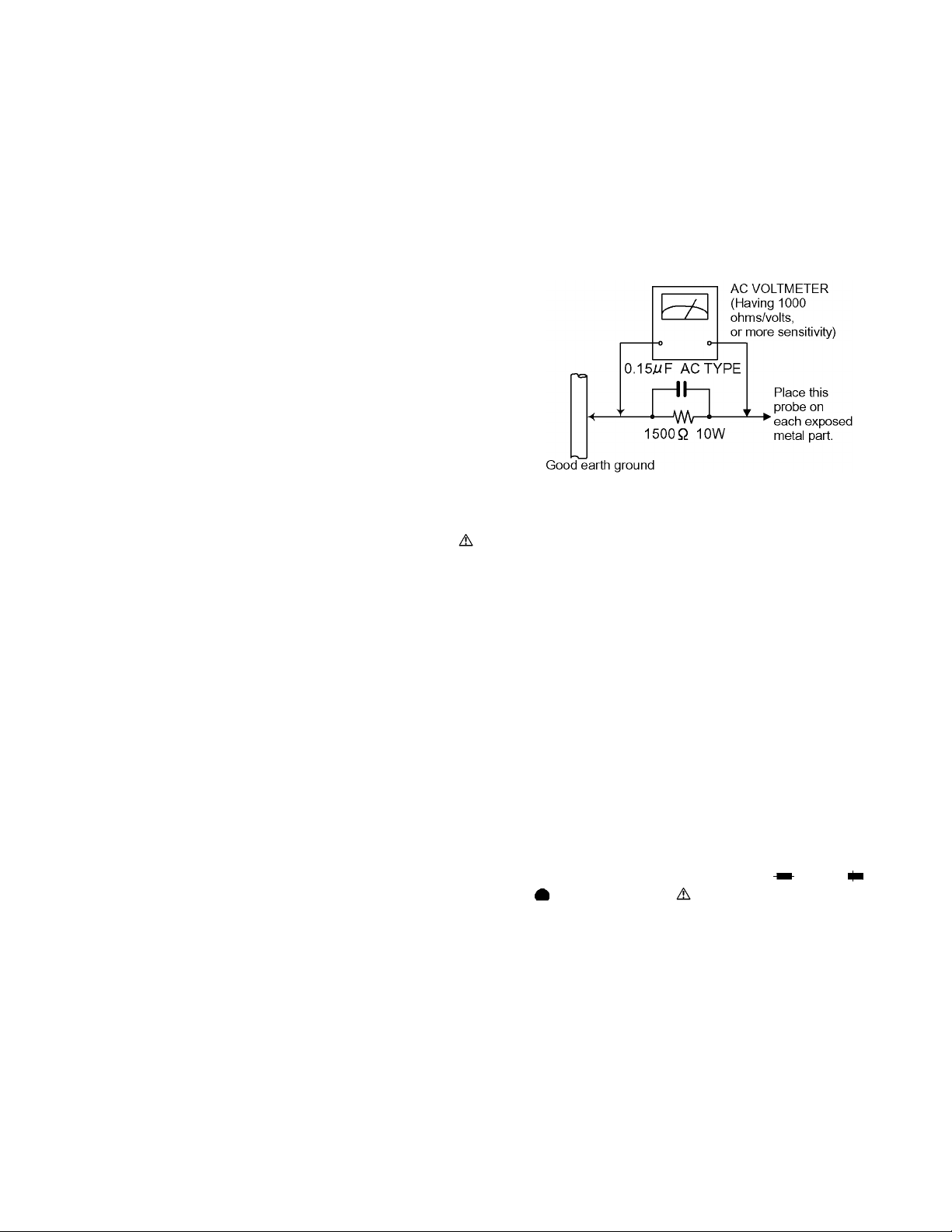
(5) Leakage shock hazard testin g)
After reassembling the product, always perform an isolation
check on the exposed metal parts of the product (antenna
terminals, knobs, metal cabinet, screw heads, headphone
jack, control shafts, etc.) to be sure the product is safe to
operate without danger of electrical shock.
Do not use a line isolation transformer during this check.
• Plug the AC line cord directly into the AC outlet. Using a
"Leakage Current Tester", measure the leakage current
from each exposed metal parts of the cabinet, particularly any exposed metal part having a return path to the
chassis, to a known good earth ground. Any leakage
current must not exceed 0.5mA AC (r.m.s.).
• Alternate check method
Plug the AC line cord direct ly into the AC outle t. Use a n AC
voltmeter having, 1,000 ohms per volt or more sensitivity in
the following manner. Connect a 1,500 ohm 10W resistor
paralleled by a 0.15 µF AC-type capacitor between an
exposed metal part and a known good earth ground.
Measure the AC voltage across the resistor with the AC
XV-FA900BK/XV-FA902SL
voltmeter.
Move the resistor connection to each exposed metal part,
particularly any exposed metal part having a return path to
the chassis, and measure the AC voltage across the
resistor. Now, reverse the plug in the AC outlet and repeat
each measurement. Voltage measured any must not
exceed 0.75 V AC (r.m.s.). This corresponds to 0.5 mA AC
(r.m.s.).
1.2 Warning
(1) This equipment has been designed and manufactured to
meet international safety standards.
(2) It is the legal responsibility of the repairer to ensure that
these safety standards are maintained.
(3) Repairs must be made in accordance with the relevant
safety standards.
(4) It is essential that safety critical components are replaced
by approved parts.
(5) If mains voltage selector is provided, check setting for lo-
cal voltage.
1.3 Caution
Burrs formed during molding may be left over on some
parts of the chassis.
Therefore, pay attention to such burrs in the case of preforming repair of this system.
1.4 Critical parts for safety
In regard with component parts appearing on the silk-screen
printed side (parts side) of the PWB diagrams, the parts that are
printed over with black such as the resistor ( ), diode ( ) and
ICP ( ) or identified by the " " ma rk nearby are critical for safety.
When replacing them, be sure to use the parts of the same type
and rating as specified by the manufacturer. (Except the JC version)
3
Page 4
XV-FA900BK/XV-FA902SL
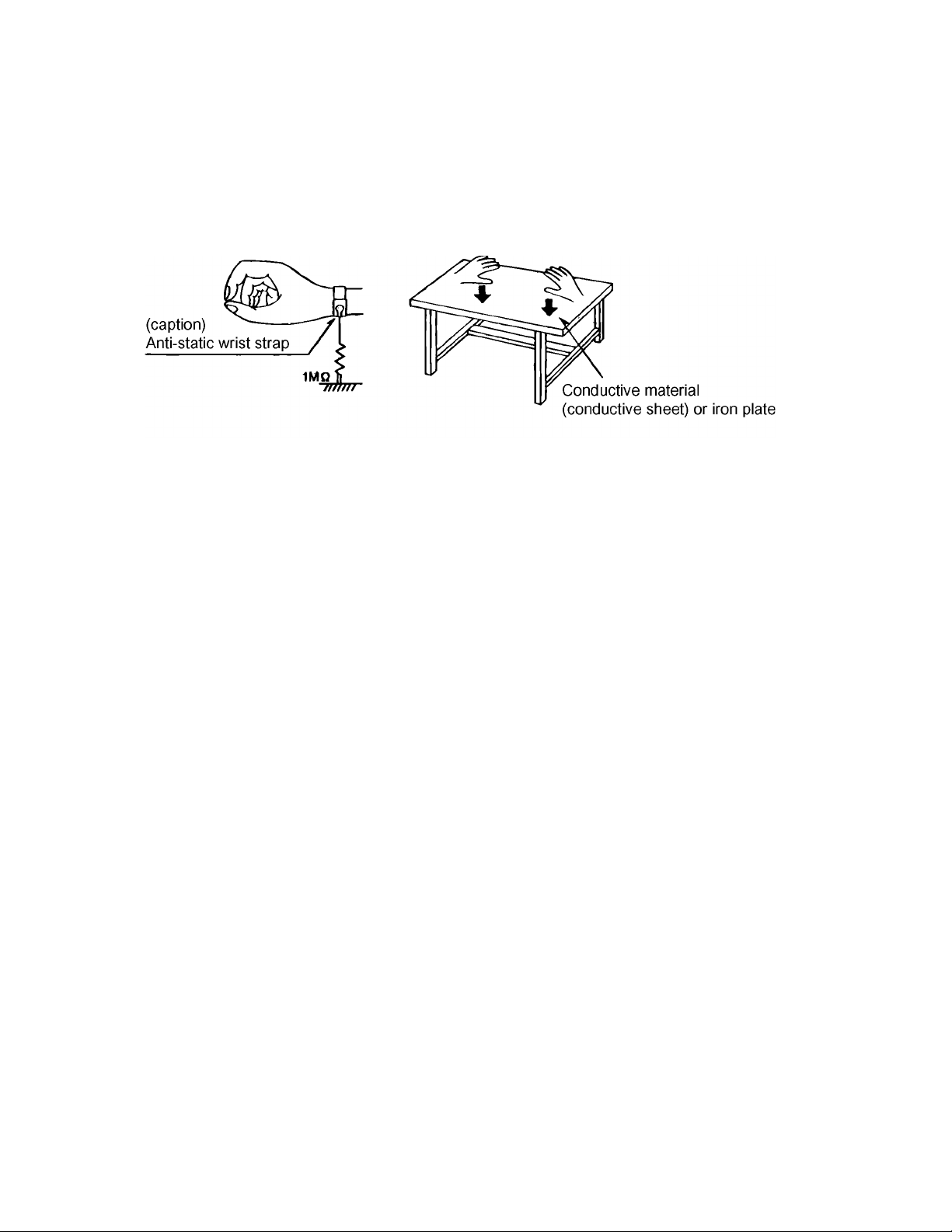
1.5 Preventing static electricity
Electrostatic discharge (ESD), which occurs when static electricity stored in the body, fabric, etc. is discharged,
can destroy the laser diode in the traverse unit (optical pickup). Take care to prevent this when performing repairs.
1.5.1 Grounding to prevent damage by static electricity
Static electricity in the work area can destroy the optical pickup (laser dio de) in devices such as DVD players.
Be careful to use proper grounding in the area where repairs are being performed.
(1) Ground the workbench
Ground the workbench by laying conductive material (such as a conductive sheet) or an iron pl ate over it before placing the
traverse unit (optical pickup) on it.
(2) Ground yourself
Use an anti-static wrist strap to release any static electricity built up in your body.
(3) Handling the optical pickup
• In order to maintain quality during transport and before installation, both sides of the laser diod e on the replacement optical
pickup are shorted. After replacement, return the shorted parts to their original condition.
(Refer to the text.)
• Do not use a tester to check the condition of the laser diode in the optical pickup. The tester's internal power source can
easily destroy the laser diode.
1.6 Handling the traverse unit (optical pickup)
(1) Do not subject the traverse unit (optical pickup) to strong shocks, as it is a sensitive, complex unit.
(2) Cut off the shorted part of the flexible cable using nippers, etc. after replacing the optical pickup. For specific details, refer to the
replacement procedure in the text. Remove the anti-static pin when replacing the traverse unit. Be careful not to take too
long a time when attaching it to the connector.
(3) Handle the flexible cable carefully as it may break when subjected to strong force.
(4)I t is not possible to adjust the semi-fixed resistor that adjusts the laser power. Do not turn it.
4
Page 5
1.7 Importance admistering point on the safety
XV-FA900BK/XV-FA902SL
5
Page 6
XV-FA900BK/XV-FA902SL
1.8 Precautions for Service
1.8.1 Handling of Traverse Unit and Laser Pickup
(1) Do not touch any peripheral element of the pickup or the actuator.
(2) The traverse unit and the pickup are precision devices and therefore must not be subjected to strong shock.
(3) Do not use a tester to examine the laser diode. (The diode can easily be destroyed by the internal power supply of the tester.)
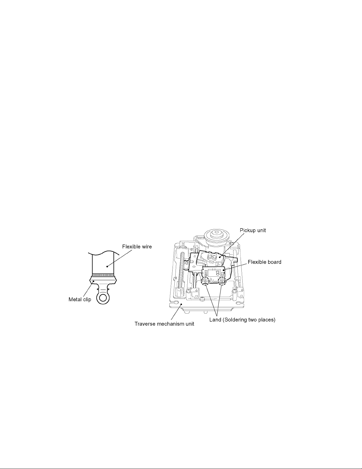
(4) To replace the traverse unit, pull out the metal short pin for protection from charging.
(5) When replacing the pickup, after mounting a new pickup, remove the solder on the short land which is pr ovided at the center
of the flexible wire to open the circuit.
(6) Half-fixed resistors for laser power adjustment are adjusted in pairs at shipment to mat ch the characteristics of the optical block.
Do not change the setting of these half-fixed resistors for laser power adjustment.
1.8.2 Destruction of Traverse Unit and Laser Pickup by Static Electricity
Laser diodes are easily destroyed by static electricity charged on clothing
or the human body. Before repairing peripheral elements of the traverse unit or pickup, be sure to take the following electrostatic
protection:
(1) Wear an antistatic wrist wrap.
(2) With a conductive sheet or a stee l plate on the workben ch on which th e traverse unit or the pick up is to be repa ired, ground
the sheet or the plate.
(3) After removing the flexible wire from the connector (CN1), short-circuit the flexible wire by the metal clip.
(4) Short-circuit the laser diode by soldering the land which is provided at the center of the flexible wire for the pickup.
After completing the repair, remove the solder to open the circuit.
Please refer to "Fig.1 of 3.2" of "Disassembly
method" for details.
6
Page 7
SECTION 2
Disassembly method
2.1 Main body
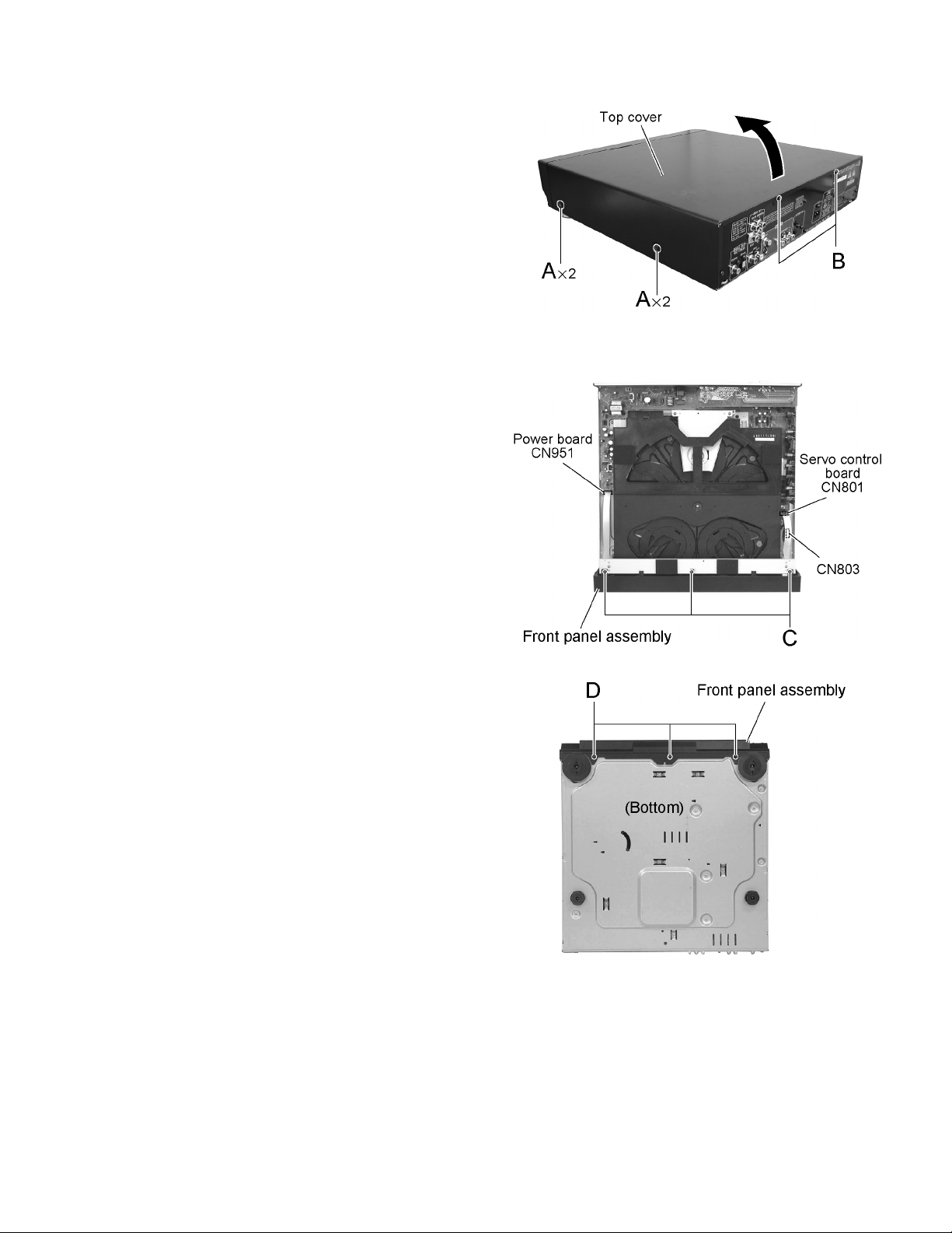
2.1.1 Removing the top cover
(See Fig.1)
(1) Remove the four screws A on each side of the body.
(2) Remove the two screws B on the back of the body.
(3) Lift the rear part of the top cover and remove in the direc-
tion of the arrow while pulling both sides of the top cover
outward.
2.1.2 Removing the front panel assembly
(See Fig.2 and 3)
• Prior to performing the following procedure, remove the top
cover.
(1) Disconnect the card wire from connector CN801 and
CN803 on the servo control board, and CN951 on the
power board respectively.
(2) Remove the three screws C on the upper side of the body.
(3) Remove the three screws D on the bottom of the body.
Remove the front panel assembly toward the front.
XV-FA900BK/XV-FA902SL
Fig.1
Fig.2
Fig.3
7
Page 8
XV-FA900BK/XV-FA902SL
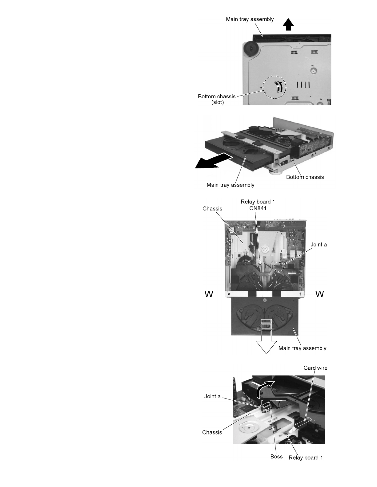
2.1.3 Removing the main tray assembly
(See Fig.4 to 7)
• Prior to performing the following procedure, remove the top
cover and the front panel assembly.
(1) Turn over the body and insert a screwdriver into the slot of
the bottom chassis, then move it in the direction of the ar-
row in Fig.4. The main tray assembly will move forward.
(2) Draw the main tray assembly toward the front manually.
(3) Bring up the joint a over the boss of the chassis, and re-
move the main tray assembly toward the front.
(4) Remove the two screws W attaching the front bracket.
(5) Disconnect the card wire, on the back of the main tray as-
sembly, from connector CN841 on the relay board 1.
Fig.4
Fig.5
Fig.6
Fig.7
8
Page 9
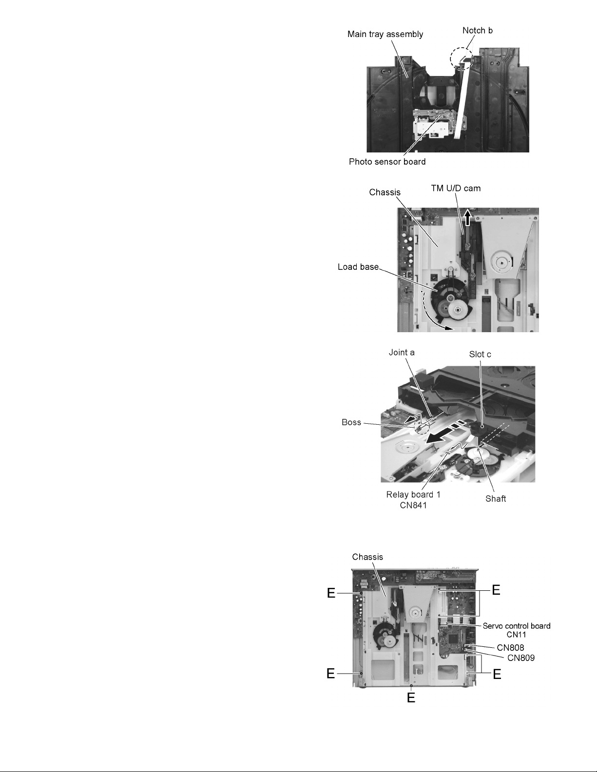
--Reattaching the main tray assembly -(See Fig.8 to 10)
(1) Turn over the main tray assembly and pass the card
wire extending from the photo sensor board through the
notch b, in advance (Fig.8).
(2) From above the chassis, turn the load base counter-
clockwise until the TM U/D cam stops at the back end
(Bring down the traverse mechanism assembly).
(3) Reattach the main tray assembly to the chassis while fit-
ting to the groove on the right and left sides of the chassis.
(4) Connect the card wire through the notch b to connector
CN841 on the relay board 1.
(5) Reattach the main tray assembly while fitting the slot c
to the shaft.
XV-FA900BK/XV-FA902SL
Fig.8
2.1.4 Removing the chassis
(See Fig.11)
• Prior to performing the following procedure, remove the top
cover, the front panel assembly and the main tray assembly.
(1) Disconnect the wire from connector CN808, CN 809 and
the card wire from CN11 on the servo control board respectively.
(2) Remove the seven screws E attaching the chassis.
Fig.9
Fig.10
Fig.11
9
Page 10
XV-FA900BK/XV-FA902SL
2.1.5 Removing the rear panel
(See Fig.12)
• Prior to performing the following procedure, remove the top
cover.
(1) Remove the fourteen screws F attaching the rear panel.
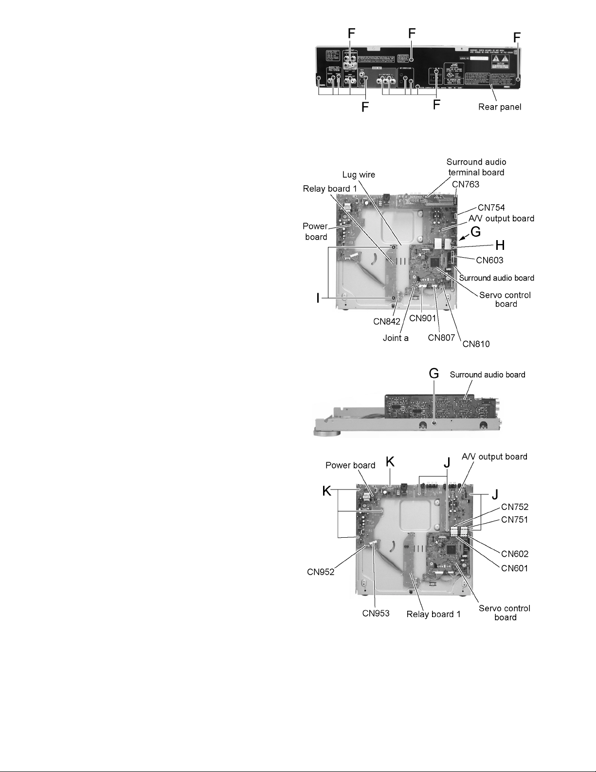
2.1.6 Removing each board
(See Fig.13 to 15)
• Prior to performing the following procedure, remove the top
cover, the front panel assembly, the main tray assembly, rear
panel and the chassis.
--Surround audio board--
(1) Pull out the surround audio terminal board from connec-
tor CN763.
(2) Remove the screw G attaching the surround audio
board.
(3) Pull out the surround audio board from connector
CN754 and CN603.
--Servo control board--
(1) Disconnect the card wire from connector CN601 and
CN602 on the servo control board.
(2) Disconnect the wire from connector CN807, CN810 and
CN901 on the servo control board respectively.
(3) Remove the screw H attaching the servo control board
and release the joint a.
--Relay board 1--
(1) Disconnect the wire from connector CN842 on the relay
board 1.
(2) Remove the two screws I attaching the relay board.
--A/V output board--
(1) Disconnect the card wire from connector CN751 and
CN752 on the A/V output board.
(2) Remove the four screws J attaching the A/V output
board.
--Power board--
(1) Disconnect the wire from connector CN952 and CN953
on the power board.
(2) Remove the four screws K on the upper side of the
body.
Fig.12
Fig.13
Fig.14
10
Fig.15
Page 11
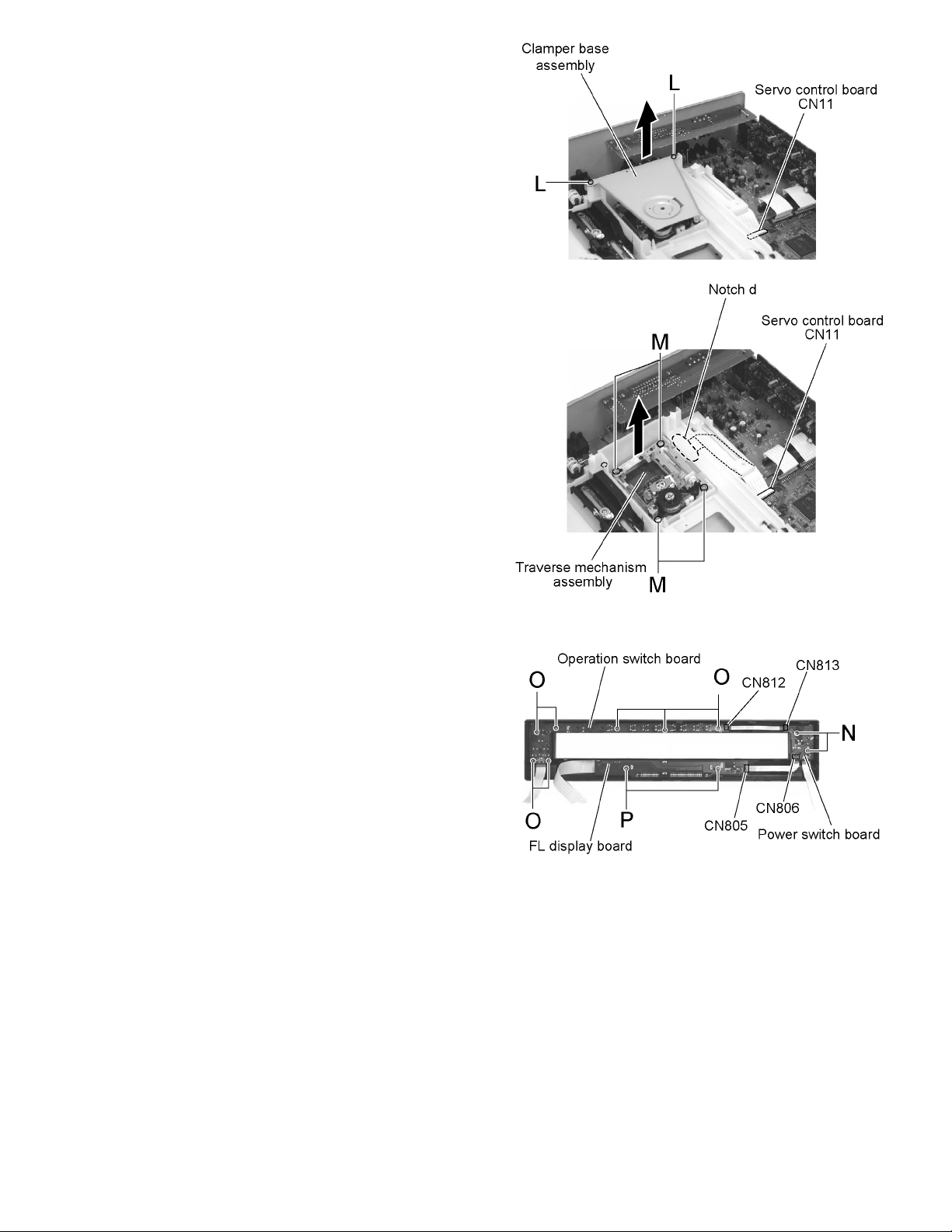
2.1.7 Removing the traverse mechanism assembly
(See Fig.16 and 17)
• Prior to performing the following procedure, remove the top
cover.
REFERENCE:
There is no need to remove the chassis.
(1) Eject the main tray assembly toward the front referri ng to
“Removing the main tray assembly”
(2) Remove the two screws L and pull out the clamper base
assembly upward.
(3) Disconnect the card wire from connector CN11 on the ser-
vo control board.
(4) Remove the four screws M and the traverse mechanism
assembly upward.
CAUTION:
When reattaching the traverse mechanism assembly, pass
the card wire extending from the traverse mechanism assembly through the notch d of the TM U/D base.
XV-FA900BK/XV-FA902SL
Fig.16
2.2 Front panel assembly
• Prior to performing the following procedure, remove the top
cover and the front panel assembly.
2.2.1 Removing the power switch board
(See Fig.18)
(1) Remove the two screws N on the back of the front panel
assembly.
(2) Disconnect the card wire from connector CN813 and
CN806 on the power switch board.
2.2.2 Removing the operation switch board
(See Fig.18)
(1) Remove the seven screws O on the back of the front pan-
el assembly.
(2) Disconnect the card wire from conn ector CN812 on the
operation switch board.
2.2.3 Removing the FL display board
(See Fig.18)
(1) Remove the two screws P on the back of the front panel
assembly.
(2) Disconnect the card wire from connector CN805 on the FL
display board.
Fig.17
Fig.18
11
Page 12
XV-FA900BK/XV-FA902SL
SECTION 3
MECHANISM
3.1 chassis unit
• Prior to p erforming the following p rocedures, remove the top
cover, the front panel assembly, the main tray assembly, the
chassis.
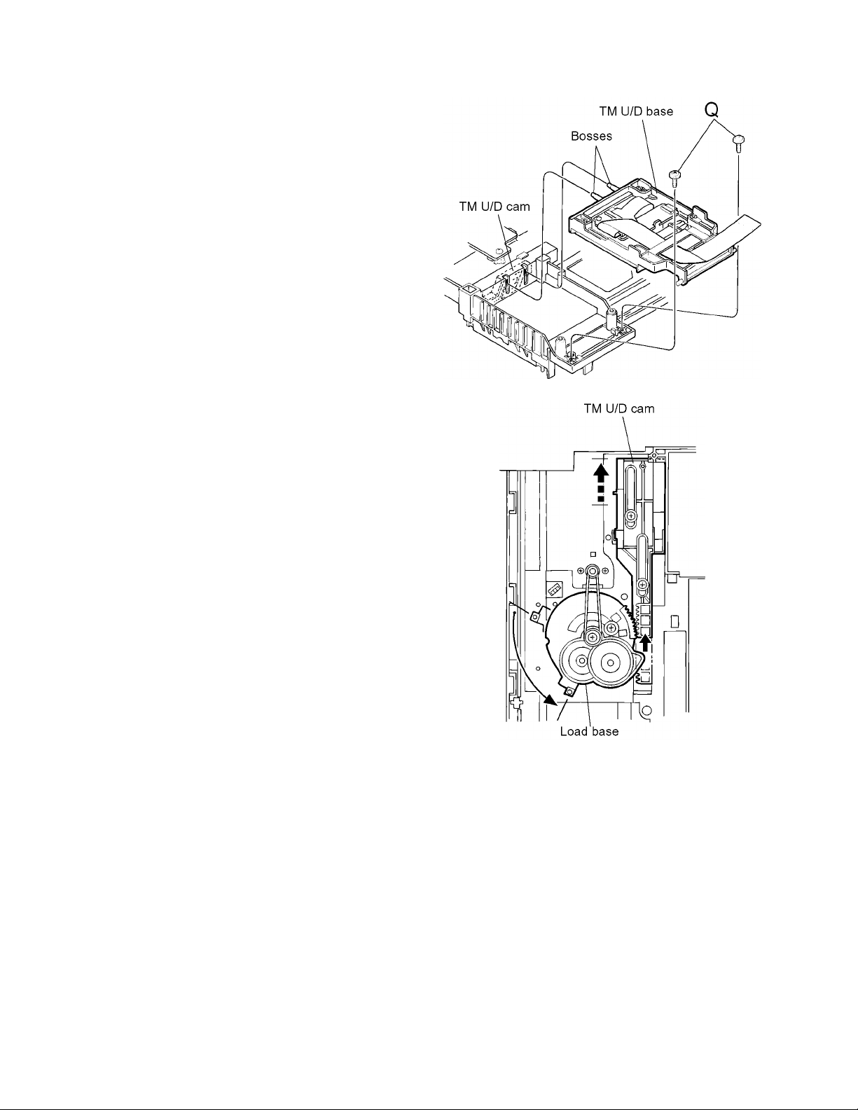
3.1.1 Removing the TM U/D base
(See Fig.1 and 2)
REFERENCE:
It is not necessary to remove the traverse mechanism assembly from the TM U/D base. As the removing procedure of the
traverse mechanism, please refer to “Removing the traverse
mechanism assembly”
(1) Turn over the chassis and remove the two screws Q.
(2) Remove the TM U/D base upward.
Reattaching the TM U/D base
REFERENCE:
From above the loading base, turn the load base counterclockwise until the TM U/D cam stops at the back end as
shown in
Fig.2.
Fig.1
(1) Reattach the TM U/D base to the chassis while fitting
the two Bosses on the side of the TM U/D base to the
grooves of the TM U/D cam.
(2) Reattach the two screws Q.
Fig.2
12
Page 13
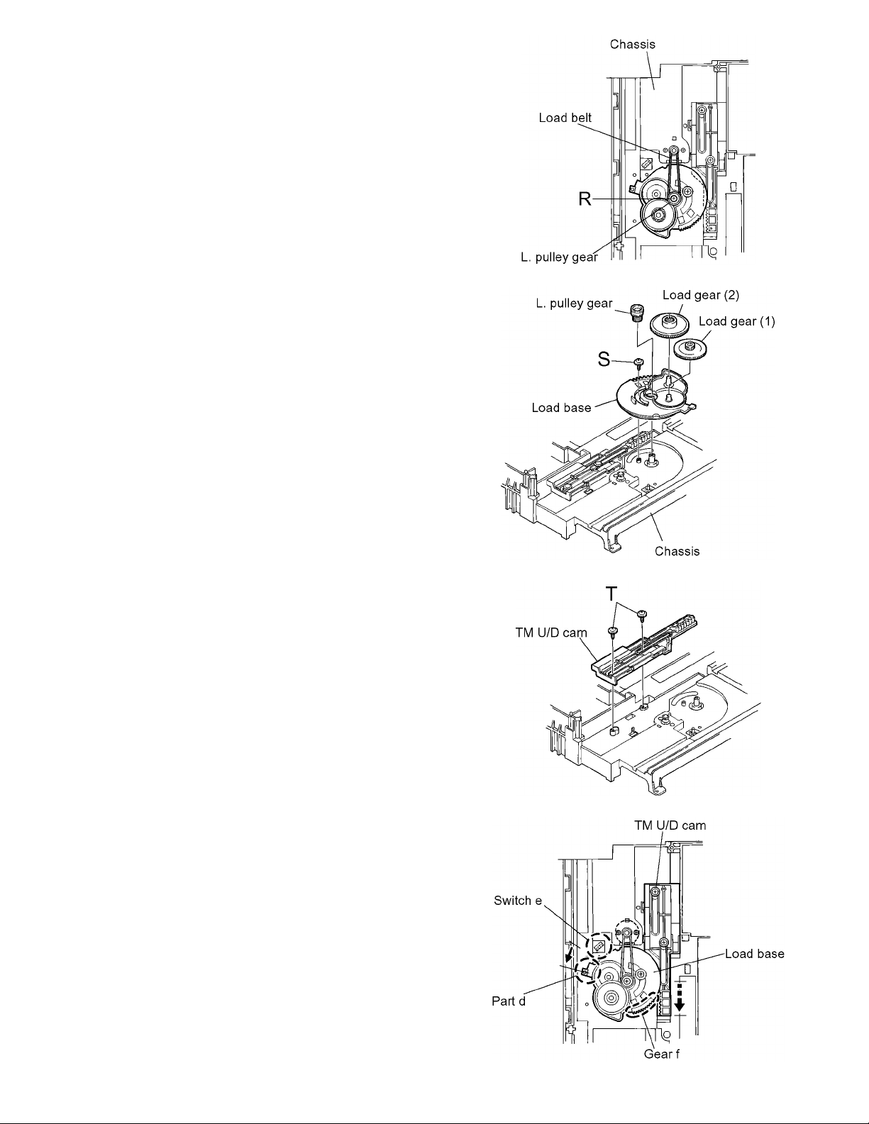
3.1.2 Removing the load belt / load base / TM U/D cam
(See Fig.3 to 6)
• Prior to performing the following procedures, remove the TM
U/D base.
(1) Remove the load belt on the upper side of the chassis.
(2) Remove the screw R attaching the L. pulley gear.
(3) Remove the L. pulley gear, the load gear (1), the load gear
(2) and the load belt respectively.
(4) Remove the screw S and the load base upward.
(5) Remove the two screws T and the TM U/D cam upward.
CAUTION:
When reattaching the TM U/D cam and the load base,
(1) Move the TM U/D cam toward the front until it stops
(Fig.6).
(2) Make sure that the part d of the load base is out of align-
ment with the switch e and that the gear f is disengaged
from the TM U/D cam.
XV-FA900BK/XV-FA902SL
Fig.3
Fig.4
Fig.5
Fig.6
13
Page 14
XV-FA900BK/XV-FA902SL
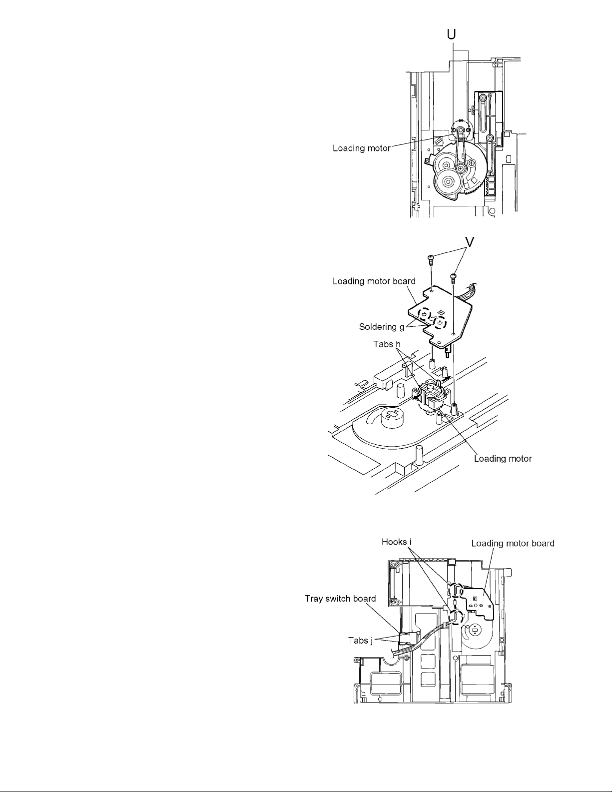
3.1.3 Removing the loading motor / loading motor board
(See Fig.7 and 8)
(1) Remove the two screws U attaching the loading motor on
the upper side of the chassis.
(2) Turn over the chassis and unsolder the two soldering g on
the loading motor board.
(3) Remove the two screws V attaching th e loading motor
board.
(4) Spread apart the two tabs h and pull out the loading motor.
CAUTION:
When reattaching the loading motor board, settle the wires on
the two hooks i on the chassis and draw the other end to the
left as shown in Fig.9.
Fig.7
3.1.4 Removing the tray switch board
(See Fig.9)
(1) Turn over the chassis, and remove the tray switch board
while spreading apart the two tabs j.
14
Fig.8
Fig.9
Page 15
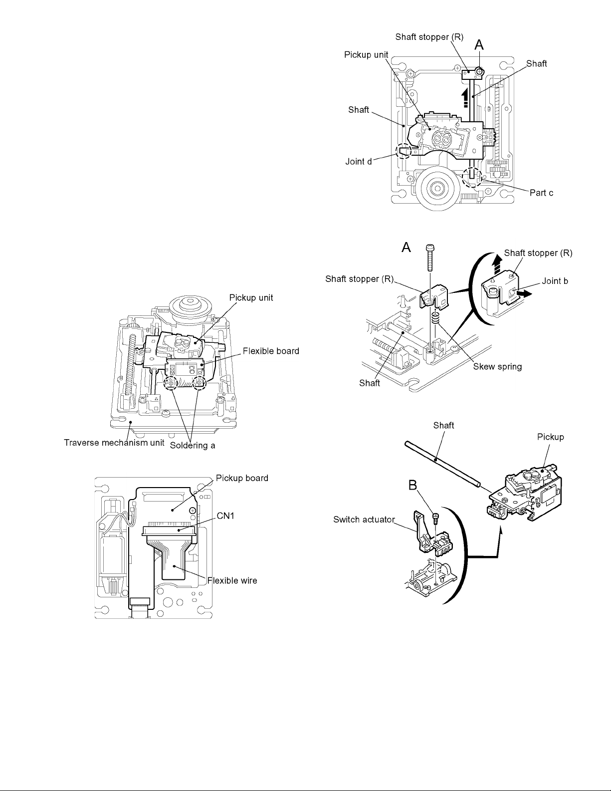
3.2 Traverse mechanism unit
3.2.1 Removing the pickup
(See Fig.1 to 5)
It is not necessary to remove the traverse mechanism unit.
(1) Solder soldering a on the flexible board next to the pickup
unit.
(2) From the bottom of the traverse mechanism unit, discon-
nect the flexible wire from CN1 on the pickup board.
ATTENTION:
Disconnecting the flexible wire without soldering may
cause damage to the pickup.
(3) Remove the screw A attaching the shaft stopper (R) on
the upper side of the traverse mechanism unit. Pull the
side of the shaft stopper (R) outward to release the joint b
and remove it upward. Remove the skew spring at the
same time.
(4) Move the shaft in the direction of the arrow to release it
from the part c.
(5) Release the joint d with the shaft and remove the pickup
with the shaft.
(6) Pull out the shaft.
(7) Remove the screw B attaching the switch actuator.
XV-FA900BK/XV-FA902SL
Fig.3
Fig.1
Fig.2
Fig.4
Fig.5
15
Page 16
XV-FA900BK/XV-FA902SL
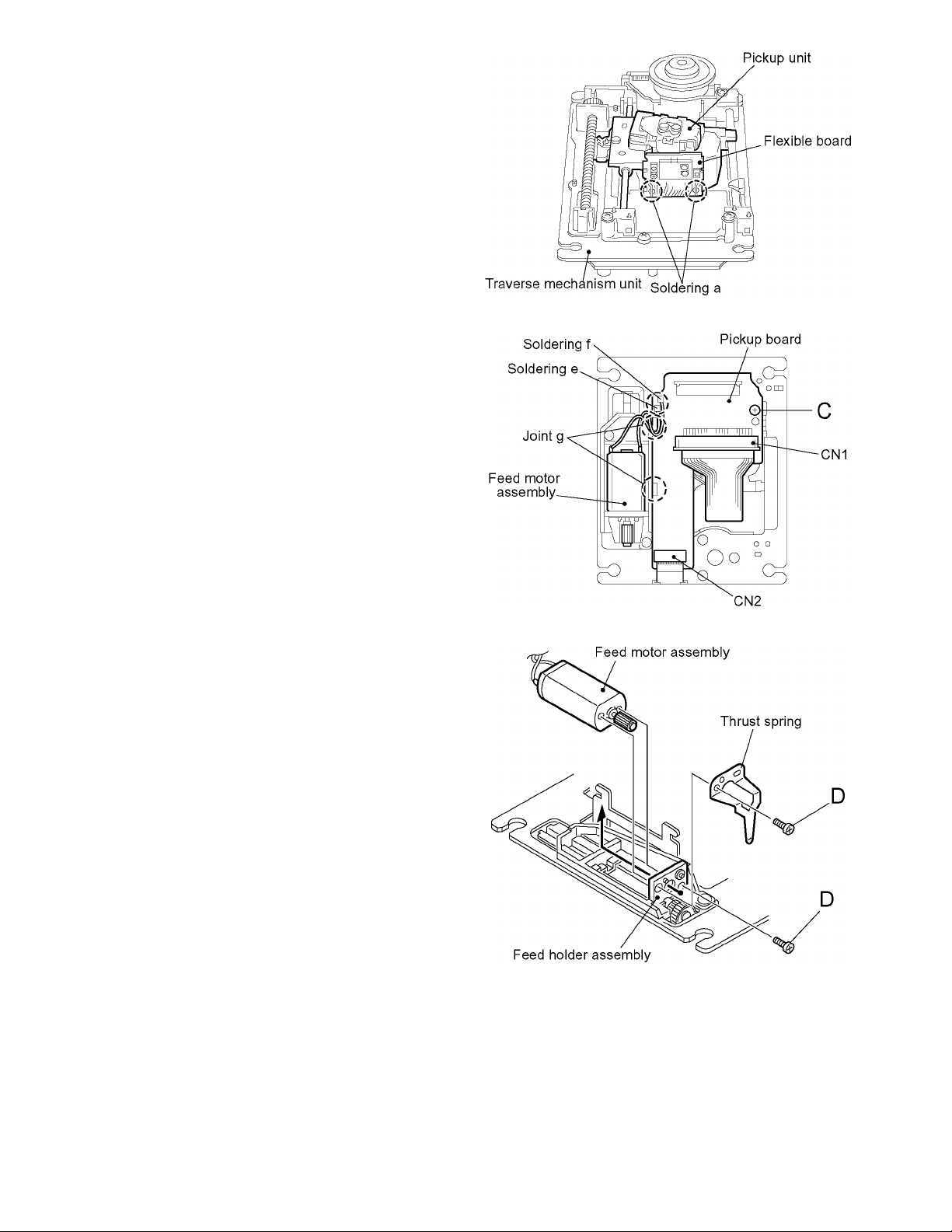
3.2.2 Removing the pickup board
(See Fig.1 and 6)
It is not necessary to remove the traverse mechanism unit.
(1) Solder soldering a on the flexible board next to the pickup
unit.
(2) From the bottom of the traverse mechanism unit, discon-
nect the flexible wire from CN1 on the pickup board.
ATTENTION:
Disconnecting the flexible wire without soldering may
cause damage to the pickup.
(3) Disconnect the card wire from connector CN2 on the pick-
up board and unsolder the soldering e and f on the harnesses
(4) Remove the screw C attaching the pickup board and re-
lease the two joints g.
3.2.3 Removing the feed motor assembly
(See Fig.1, 6 and 7)
• Prior to performing the following procedure, remove the
traverse mechanism unit.
(1) Solder soldering a on the flexible board next to the pickup
unit.
(2) From the bottom of the traverse mechanism unit, discon-
nect the flexible wire from CN1 on the pickup board.
ATTENTION:
Disconnecting the flexible wire without soldering may
cause damage to the pickup.
Fig.1
(3) Remove the pickup board.
(4) Remove the two screws D attaching the feed motor a s-
sembly and remove the thrust spring. Move the feed motor
assembly in the direction of the arrow to pull it out from the
feed holder.
Fig.6
Fig.7
16
Page 17
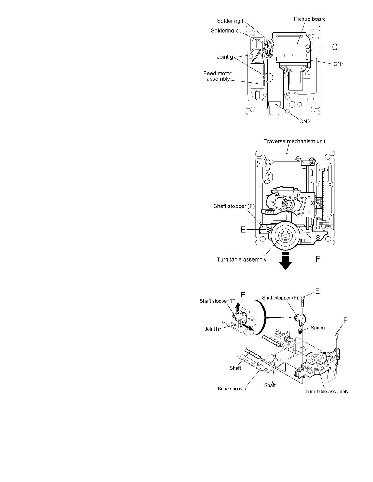
3.2.4 Removing the turn table assembly
(See Fig.6, 8 and 9)
• Prior to performing the following procedure, remove the
traverse mechanism unit.
(1) Disconnect the card wire extending from the turn table as-
sembly, from connector CN2 on the pickup board.
(2) Remove the screw E attaching the shaft stopper (F) on the
upper side of the traverse mechanism unit. Pull the side of
the shaft stopper (F) outward to release the joint h and re-
move it upward. Remove the spring at the same time.
(3) Remove the screw F attaching the turn table assembly.
(4) Move the turn table assembly outward and pull out from
the shaft. Then remove it from the base chassis.
XV-FA900BK/XV-FA902SL
Fig.6
Fig.8
Fig.9
17
Page 18

XV-FA900BK/XV-FA902SL
3.3 Main tray assembly unit
• Prior to p erforming the following p rocedures, remove the top
cover, the front panel assembly and the main tray assembly.
3.3.1 Removing the fitting (See Fig.1)
(1) Remove the fitting on the front side of the main tray as-
sembly while releasing the four joints a upward.
3.3.2 Removing the main tray cover and the main tray
(See Fig.2 and 3)
• Prior to performing the following procedure, remove the fitting.
(1) Remove the six screws A attaching the main tray on the
under side of the main tray assembly.
(2) Remove the screw B attaching the main tray cover on the
upper side of the main tray assembly.
(3) Push the two joint tabs b on the back of the main tray as-
sembly to release the main tray cover from the tray bottom. Disengage the joint tabs c of the main tray from the
main tray cover.
Fig.1
18
Fig.2
Fig.3
Page 19

3.3.3 Removing the photo sensor board and the sub tr ay
drive motor assembly
(See Fig.4)
(1) Turn over the main tray assembly and remove the two
screws C attaching the photo sensor board.
(2) Disconnect the card wire from conn ector CN082 on the
photo sensor board.
REFERENCE:
Make sure to disconnect the card wire from the photo
sensor board. If the photo sensor board is pulled out
from the main tray without disconnecting the card wire,
the cam switch side inside of the main tray may be damaged.
(3) Remove the two screws D attaching the motor base unit.
--When reassembling,--
• Attach the two wires to the part d on the photo sensor
board, and before reattaching the photo sensor board, connect the card wire to connector CN082 and pass the card
wire extending from connector CN081 through the notch e
of the main tray.
XV-FA900BK/XV-FA902SL
Fig.4
19
Page 20

XV-FA900BK/XV-FA902SL
3.3.4 Sub tray position and operation check
(See Fig.5 and 6)
• Prior to performing the following procedures, remove the fit-
ting and the main tray cover.
CAUTION:
Make sure the sub trays are set as shown in Fig.5. When moving the sub trays, put the sub trays which come to the position
(4) and (5) forward in turn.
Prior to moving the sub trays by hand, the sub tray drive motor
assembly must be removed in advance referring to the preceding page.
Do not put the sub trays forward except at the position (4) and
(5).
3.3.5 Removing the U/D cam (U)
(See Fig.7)
• Prior to performin g the fo llo wing pr ocedure, re mo ve the main
tray cover.
(1) Remove the two screws E attach ing the U/D cam (U) on
the upper side of the main tray assembly.
Fig.5
20
Fig.6
Fig.7
Page 21

3.3.6 Removing the sub trays (See Fig.8 to 14)
• Prior to performing the following procedure, remove the main
tray cover and the U/D cam (U).
CAUTION:
Remove the sub tray assembly (4), (3), (2), (5), (6), (7) and (1)
in order. When reattaching, observe the following procedure
without fail.
(1) Remove the sub tray (4) and (3) from the main tray up-
ward.
(2) Remove the sub tray (2) upward.
(3) Similarly, remove the sub tray (5) , (6) and (7) upward.
(4) At last, remove the sub tray (1) upward.
--Reattaching the sub tray--
(1) Reattach the sub tray (1) while fitting the part f to the
groove of the ACT. gear (1) marked g.
(2) Reattach the sub tray (2) while inserting the shaft h into
the groove i of the main tray, and at the same ti me, fitting the part j to the groove of the ACT. gear (1) marked
k .
Move the sub tray (2) toward the tray (1).
(3) Similarly, reattach the sub tray (7).
XV-FA900BK/XV-FA902SL
Fig.8
Fig.9
Fig.10
21
Page 22

XV-FA900BK/XV-FA902SL
(4) Reattach the sub tray (3) while inserting the shaft l into
the groove m of the main tray, and at the same time,
putting the shaft n on the U/D cam (L). Then, move the
sub tray (3) toward the sub tray (2) until it stops.
REFERENCE:
At this point, the sub tray (3) is on top of the sub tray
(2).
(5) Reattach the sub tray (4) while fitting the part o to the
ACT.gear (2) on the main tray.
CAUTION:
Make sure the part o of the sub tray (4) engages with
the ACT. gear (2) correctly in the center of the main
tray.
REFERENCE:
At this point, the sub tray (4) is on top of the sub tray
(3).
(6) Reattach the sub tray (6) and (5) in the same way.
CAUTION:
Make sure that the trays are attached to the correct
position and that they can be moved. To move the sub
trays manually, the sub tray drive motor assembly
must be removed in advance.
Fig.11
Fig.12
Fig.13
22
Fig.14
Page 23

3.3.7 Removing the cam switch board assembly
(See Fig.15 to 17)
• Prior to performing the following procedure, remove the main
tray cover, the U/D cam (U) and the sub trays.
(1) Remove the screw F attaching the gear cover. Release
the two tabs marked p by pushing inward.
(2) Remove the cam gear (2) upward.
(3) Disconnect the card wire from conn ector CN083 on the
cam switch board assembly.
(4) Remove the two screws G attaching the cam switch board
assembly.
CAUTION:
When reattaching the cam gear (2), set the position of the
boss and the triangular mark and hole as shown in Fig.17.
XV-FA900BK/XV-FA902SL
Fig.15
Fig.16
Fig.17
23
Page 24

XV-FA900BK/XV-FA902SL
3.3.8 Removing the ACT. gear (1), U/D cam (L), cam gear
(1) and ACT.gear (2)
(See Fig.18 and 19)
• Prior to performin g the fo llo wing pr ocedure, re mo ve the main
tray cover, the U/D cam (U) and the sub trays.
(1) Draw out the U/D cam (L).
(2) Draw out the ACT. gear (1).
(3) Draw out the cam gear (1).
(4) Draw out the ACT. gear (2) while pushing the two inward.
CAUTION:
When reassembling, make sure the position of each gear referring to Fig.19 and reattach the ACT. gear (2) first.
Fig.18
24
Fig.19
Page 25

SECTION 4
Adjustment method
4.1 Tes t mode setting method
(1) Take out the disc and close the tray.
(2) Unplug the power plug.
(3) Insert power plug into outlet while pressing both "PLAY" button and "STOP" button of the main body.
(4) The player displays "TEST * * " on the FL display. keeps pushing the button until this is displayed.
" * * " means the player version.
(5) When the power supply is turned off, test mode is released.
The mode changes as follows whenever the "CHOICE" button of remote controller is pushed in test mode.
XV-FA900BK/XV-FA902SL
4.2 Initialization method
Please initialize according to the following procedures when mic roprocessor or pick-up is exchanged and wh en the up-
grade is done.
(1) Makes to test mode.
(2) After "FORWARD SKIP" button ( ) of the main body is pushed, "PAUSE" button is pushed.
(3) DVD AUDIO indicator lights when about ten seconds pass. Then, it is initialization comp letion.
4.3 Method of displaying version of microcomputer
(1) Makes to test mode and initializes
(2) When "CHOICE" button of remote controller is pushed once, the figure is displayed on the FL display as follows.
* Version number of decoder is displayed on the television screen.
* Last two digits are displayed on the FL display for the treble version number.
4.4 Method of displaying device key index
(1) Makes to test mode and initializes.
(2) When "CHOICE" button of remote controller is pushed twice, the device key index is displayed on the
FL display as follows.
25
Page 26

XV-FA900BK/XV-FA902SL
4.5 Display of current value of laser
(1) Makes to test mode and initializes.
(2) When "CHOICE" key of remote controller is pushed four times, It is displayed on the FL display, "CHECK".
(3) Afterwards, the laser current value can be switched by pushing the key to remote controller without turning on the disc.
Remote controller "4" key --- Laser of DVD
Remote controller "5" key --- Laser of CD
As for the current value of the laser, the figure displayed on
the FL display becomes a current value as it is by "mA" unit.
becomes 36 mA if displayed as 36.
(4) The laser output stops if the "STOP" key to remote controller is pushed.
It can be judged it is simply good if the displayed current value of the laser is smaller than that of the undermentioned value.
Moreover, there must be a deteriorated possibility and the pick-up must exchange the pick-up more than the
undermentioned value.
Laser current value of CD ------ 49 mA or less
Laser current value of DVD ---- 64 mA or less
4.6 Display of jitter value
(1) Makes to test mode and initializes.
(2) When "CHOICE" key of remote controller is pushed four times, It is displayed on the FL display, "CHECK".
(3) The test disk (VT-501) is inserted, and the "PLAY" key to the main body is pushed.
(4) The jitter value is displayed on the FL display as follows.
Values to judge whether the jitter is allowa ble or not is displayed, instead of actual
jitter values.The displayed values are expressed in hexadeci mal numbe rs.
In the following cases, please "Flap adjustment of the pick-up guide shaft" referring to the following page.
Before using the TEST disc VT-501, careful check it if there is neither damage nor dirt on the read surface.
< In the following cases, please adjustment >
• When you exchange the pick-up
• When you exchange the spindle motor
• When the reading accuracy of the signal is bad (There is a block noise in the screen etc..)
26
Page 27

XV-FA900BK/XV-FA902SL
4.7 Flap adju stment of the pick-up guide shaft
<Tool list for adjustment>
Stud (four pieces set)
Parts No. : JIGXVS40
Hex wrench for adjustment
Off-the-shelf (1.3mm)
Test disc
VT-501 or VT-502
<Adjustment preparation>
(1) The metal cover is detached, the "OPEN/CLOSE" button is pushed, and the tray is done in open.
(2) The AC plug code is pulled out once in the state.
(3) Remove the surround audio board and surround audio terminal board respectively.
(4) The traverse mechanism is detached, and the card wire is connected with CN11.
(5) The stud is installed in the traverse mechanism as shown in Figure.
The clamper is removed from the clamper base.
(6) The disk (Everything is good) is put on sub-tray 1, the test disk is put on the turntable in the traverse mechanism, and fixes by
the clamper.
(7) The card wire becomes under the main tray, and the main tray is closed by hand operated.
(8) The AC plug code is inserted, and the "DISC1" button is pushed
(Please push the "DISC1" button directly without pushing the power supply button).
(9) Because the playback of "DISC1" starts, stops and the AC plug code is pulled out.
<Adjustment method>
(10) The AC plug code is made insertion test mode while pu shing the "PLAY" button and the "STOP" button of the main body at
the same time.
(11) Please push the "PAUSE" button after pushing the "FORWARD SKIP" button of the main body, and confirm
DVD AUDIO indicator lights after a few seconds.
(12) When the "CHOICE" button of remote controller is pushed three times, it is displayed on the FL display as
"CHECK".
(13) The display of the FL display changes into "CHECK OK" after a few seconds if the "PAUSE" button of the main body is pushed
in the state.
When the "PLAY" button of the main body is pushed afterwards, the jitter value is displayed on the FL display.
<Adjustment>
(1) Puts into the state to display the jitter value on the FL display referring to "Displa y of jitter value" .
(2) The adjustment screw under the traverse mechanism is turned with hex wrench, and matches so that the jitter value dis-
played on the FL display may become maximum value.
<POINT>
(1) turns in the forward or the opposite direction, and
makes to the position where the jitter value is good
the half rotation of adjustment screw a and b(180 degrees) respectively.
(2) Afterwards, adjustment screw b and c are turned in
the same way, and makes to the best position.
* As this value is bigger, the jitter is more allowable in
this model.
27
Page 28

XV-FA900BK/XV-FA902SL
4.8 Upgrading of firmware
(1) The power supply is turned on pushing the "P OWER" key.
(2) The up-grade disc is inserted.
(3) When FL display of the main body changes from "READING" into "UPGRADE", cursor "UP" key ( ) of remote controller
is pushed.
(4) The up-grade starts if the entire screen becomes blue and it is displayed, "Upgrade progress".
(5) The tray opens automatically, the up-grade disc is removed.
(6) The up-grade ends if the tray closes automatically, and the screen returns to the normal screen.
(7) Please confirm the version of the microcomputer after makes to test mode and initializes.
4.9 Display of region code
(1) Makes to the stand-by state.
(2) The "POWER" key is pushed while pushing the "BACK SKIP" key and the "FORWARD SKIP" key to the main body.
(3) Region code is displayed on the FL display as follows.
< ATTENTION ! >
Please pull out the AC plug code after the standby indicator lights pushing the power supply button without fail after
completing the repair.
The mechanism becomes initialed position.
There is a possibility to break when carrying in not initialed position the mechanism but the state.
28
Page 29

4.10 Confirm method of operation
Please confirm the operation of the undermentioned item after doing the repair and
the upgrade of the firmware.
The EEPROM is initialized.
Refer to the initialization method.
Opening picture check (Power ON)
It should be display "JVC"
Muting working
The noise must not be had to the performance beginning when you push "PLAY" button or at ON/STANDBY.
FL Display
The mark and the logo, etc. displayed by each operation must be displayed correctly.
FL Display should light correctly without any unevenness.
All Function button
All function buttons should worked correctly with moderate click feeling.
Open and close movement of tray
When press OPEN/CLOSE button the tray should move smoothly without any noise.
XV-FA900BK/XV-FA902SL
Remote controller unit working
Check the correctly operation in use of remote controller unit.
Reading of TOC
Be not long in the malfunction.
Search
Both forward-searches and backward-searches should be able to be done.
Do not stop be searching or after the search.
Skip
Both forward-skip and backward-skip should be able to be done.
Do not stop be after the skip.
Playback
Do not find abnormality etc. of tone quality and the picture quality.
Most outside TITLE playback check
Play VT-501 TITLE 59 CHAPTER 1 , check normal playback.
29
Page 30

XV-FA900BK/XV-FA902SL
4.11 Troubleshooting
Servo volume
30
Page 31

XV-FA900BK/XV-FA902SL
4.12 Check points for each error
4.12.1 Spindle start error
(1) Defective spindle motor
*Are there several ohms resistance between each pin of CN11 "7-6","6-5","7-5"?
(The power supply is turned off and measured.)
*Is the sign wave of about 100mVp-p in the voltage had from each terminal?
[ CN11"10"(H1-),"9"(H1+),"12"(H2-),"11"(H2+),"14"(H3-),"13"(H3+) ]
(2) Defective spindle motor driver (IC251)
*Has motor drive voltage of a sine wave or a rectangular wave gone out to each terminal(SM1~3) of CN11"5,6,7" and
IC251"2,4,7"?
*Is FG pulse output from the terminal of IC251"24"(FG) according to the rotation of the motor?
*Is it "L(about 0.9V)" while terminal of IC251"15"(VH) is rotating the motor?
(3) Has the control signal come from servo IC or the microcomputer?
*Is it "L" while the terminal of IC251"18"(SBRK) is operating?
Is it "H" while the terminal of IC251"23"(/SPMUTE) is operating?
*Is the control signal input to the terminal of IC251"22"(EC)?
(changes from VHALF voltage while the motor is working.)
*Is the VHALF voltage input to the terminal of IC251"21"(ECR)?
(4) Is the FG signal input to the servo IC?
*Is FG pulse input to the terminal of IC301"69"(FG) according to the rotation of the motor?
4.12.2 Disc Detection, Distinction error (no disc, no RFENV)
<About frontend section>
* Laser is defective.
* Front End Processor is defective (IC101).
* APC circuit is defective. --- Q101,Q102.
* Pattern is defective. --- Lines for CN11 - All patterns which relate to pick-up and patterns between IC101
* Servo IC is defective (IC301). * IC101 --- For signal from IC101 to IC301, is signal output from IC101 "20" (ASOUT) and
IC101 "41"(RFENV) and IC101 "22" (FEOUT)?
<About loading mechanism section>
* The disc exists in a sub tray. However, a sub tray is sent as follows the turntable without rising.
(Especially, when the disk is CD-RW)
--- IC81 is defective. Exchanges for "GP2S28J" of the rank specification parts.
4.12.3 Traverse movement NG
(1) Defective traverse driver
*Has the voltage come between terminal of CN11 "28" and "30" ?
(2) Defective BTL driver (IC201)
*Has the motor drive voltage gone out to IC201"17" or "18"?
(3) Has the control signal come from servo IC or the microcomputer?
*Is it "H" while the terminal of IC201"9"(STBY1) ?
*TRSDRV Is the signal input? (IC301 "67")
(4) TRVSW is the signal input from microcomputer? (IC401 "50")
4.12.4 Focus ON NG
* Is FE output ? --- Pattern, IC101
* Is FODRV signal sent ? (R209) --- Pattern, IC301 "115"
* Is driving voltage sent ?
IC201 "13", "14" --- If NG, pattern, driver, mechanical unit .
* Mechanical unit is defective.
4.12.5 Tracking ON NG
* When the tracking loop cannot be drawn in, TE shape of waves does not settle.
* Mechanical unit is defective.
Because the self adjustment cannot be normally adjusted, the thing which cannot be normally drawn in is thought.
* Periphery of driver (IC201)
Constant or IC it self is defective.
* Servo IC (IC301)
When improperly adjusted due to defective IC.
4.12.6 Spindle CLV NG
* IC101 -- "35"(RF OUT), "30"(RF-), "31(RF+).
* Does not the input or the output of driver's spindle signal do the grip?
* Has the tracking been turned on?
* Spindle motor and driver is defective.
* Additionally, "IC101 and IC301" and "Mechanism is defective(jitter)", etc. are thought.
31
Page 32

XV-FA900BK/XV-FA902SL
4.12.7 Address read NG
* Besides, the undermentioned cause is thought though specific of the cause is difficult because various factors are thought.
Mechanism is defective. (jitter)
IC301, IC401.
The disc is dirty or the wound has adhered.
4.12.8 Between layers jump NG (double-layer disc only)
Mechanism defective
Defect of driver's IC(IC201)
Defect of servo control IC(IC301)
4.12.9 Neither picture nor sound is output
(1) It is not possible to search
*Has the tracking been turned on?
*To "4.10.5 Tracking ON NG" in "Check points for each error" when the tracking is not normal.
*Is the feed operation normal?
To "4.10.3 traverse movement NG" in "Check points for each error" when it is not normal.
Are not there caught of the feeding mechanism etc?
4.12.10 Picture is distorted or abnormal sound occurs at intervals of several seconds.
Is the feed operation normal?
Are not there caught of the feeding mechanism etc?
4.12.11 Others
The image is sometimes blocked, and the imag e stop s.
The image is blocked when going to outer though it is normal in
surroundings in the disk and the stopping symptom increases.
4.12.12CD During normal playback operation
a) Is TOC reading normal?
Displays total time for CD-DA.
Shifts to double-speed mode for V-CD.
b) Playback possible? *--:-- is displayed during FL search.
According to [It is not possible to search ] for DVD, check the feed and
tracking systems.
*No sound is output although the time is displayed.(CA-DA)
DAC, etc, other than servo.
*The passage of time is not stable, or picture is abnormal.(V-CD)
*The wound of the disc and dirt are confirmed.
There is a possibility with bad jitter
value for such a symptom.
32
Page 33

Description of major ICs
5.1 AN870 3FH-V (IC101) : Frontend processor
• Pin layout
• Pin function
XV-FA900BK/XV-FA902SL
SECTION 5
Pin No.
10 IDGT I Data slice part address part gate signal in-
11 STANDBY I Standby mode control terminal 46 TESTSG I TEST signal input terminal
12 SEN I SEN(Serial data input terminal) 47 RFINP I RF signal positive input terminal
13 SCK I SCK(Serial data input terminal) 48 RFINN I RF signal negative input terminal
14 STDI I STDI(Serial data input terminal) 49 VIN5 I Internal four-partition (CD) RF input 1
15 RSCL I Standard electric current terminal 50 VIN6 I Internal four-partition (CD) RF input 2
16 JLINE I Electric current setting terminal of JLine 51 VIN7 - Internal four-partition (CD) RF input 3
17 TEN I Reversing input terminal of tracking error
18 TEOUT O Tracking error signal output terminal 53 VIN9 I External two-partition (DVD) RF input 2
19 AGCBAL I Offset adjusting terminal 1 54 VIN10 I External two-partition (DVD) RF input 1
20 ASOUT O Full adder signal output terminal 55 VCC1 - Power supply terminal 5V
21 FEN I Focus error output amplifier reversing input
22 FEOUT O Focus error signal output terminal 57 VIN1 I Internal four-partition (DVD) RF input 1
23 AGCOFST I Offset adjusting terminal 2
24 MON - Non connect 58 VIN2 I Internal four-partition (DVD) RF input 2
25 AGCLVL O Output amplitude adjustment for DRC
26 GND2 - Connect to GND 59 VIN3 I Internal four-partition (DVD) RF input 3
27 VREF2 O VREF2 voltage output terminal
28 VCC2 - Power supply terminal 5V 60 VIN4 I Internal four-partition (DVD) RF input 4
29 VHALF O VHALF voltage output terminal
30 DFLTON O Reversing output terminal of filter AMP. 61 GND1 - Connect to GND
31 DFLTOP O Filter AMP. output terminal 62 VIN11 I 3 beam sub input terminal 2 (CD)
32 DCFLT I Capacity connection terminal for filter out-
33 GND3 - Connect to GND 64 HDTYPE O HD Type selection
Symbol I/O Description
1 LPC1 I Laser input terminal (DVD) 34 RFDIFO - Non connect
2 LPC01 O Laser drive signal output terminal (DVD) 35 RFOUT - Connect to TP103
3 LPC2 I Laser input terminal (CD) 36 VCC3 - Power supply terminal 3.3V
4 LPC02 O Laser drive signal output terminal (CD) 37 RFC O Filter for RF delay correction AMP.
5
VFOSHORT
6 TBAL I Tracking balance control terminal 39 OFTR O OFTR output terminal
7 FBAL I Focus balance control terminal 40 BDO O BDO output terminal
8 POFLT O Track detection threshold level terminal 41 RFENV O RF envelope output terminal
9 DTRD I Data slice part data read signal input termi-
I VFOSHORT control terminal 38 DCRF O All addition amplifier capacitor terminal
nal(For RAM)
put terminal( For RAM)
output AMP.
terminal
put
Pin No.
42 BOTTOM O Bottom envelope detection filter terminal
43 PEAK O Peak envelope detection filter terminal
44 AGCG O AGC amplifier gain control terminal
45 AGCO O A GC amplifier level control terminal
52 VIN8 - Internal four-partition (CD) RF input 4
56 VREF1 O VREF1 voltage output terminal
63 VIN12 I 3 beam sub input terminal 1 (CD)
Symbol I/O Description
33
Page 34

XV-FA900BK/XV-FA902SL
5.2 BA5983FM-X (IC201) : 4CH Driver
• Block diagram
• Pin function
Pin No.
10 PowVcc1 - Vcc for CH1/2 power block 25 OPOUT4 O Output for CH4 OP-AMP
11 VO2(-) O Inverted output of CH2 26 OPIN4(-) I Inverting input for CH4 OP-AMP
12 VO2(+) O Non inverted output of CH2 27 OPIN4(+) I Non inverting input for CH4 OP-AMP
13 VO1(-) O Inverted output of CH1 28 PreVcc - Vcc for pre block
14 VO1(+) O Non inverted output of CH1 29 - Connect to ground
15 VO4(+) O Non inverted output of CH4 30 - Connect to ground
5.3 74LCX373MTC-X(IC512,IC513)
• Pin layout
Symbol I/O Description
1 BIAS IN I Input for Bias-amplifier 16 VO4(-) O Inverted output of CH4
2 OPIN1(+) I Non inverting input for CH1 OP-AMP 17 VO3(+) O Non inverted output of CH3
3 OPIN1(-) I Inverting input for CH1 OP-AMP 18 VO3(-) O Inverted output of CH3
4 OPOUT1 O Output for CH1 OP-AMP 19 PowVcc2 - Vcc for CH3/4 power block
5 OPIN2(+) I Non inverting input for CH2 OP-AMP 20 STBY2 I Input for Ch4 stand by control
6 OPIN2(-) I Inverting input for CH2 OP-AMP 21 GND - Substrate ground
7 OPOUT2 O Output for CH2 OP-AMP 22 OPOUT3 O Output for CH3 OP-AMP
8 GND - Substrate ground 23 OPIN3(-) I Inverting input for CH3 OP-AMP
9 STBY1 I Input for CH1/2/3 stand by control 24 OPIN3(+) I Non inverting input for CH3 OP-AMP
Pin No.
Symbol I/O Description
• Truth table
INPUTS OUTPUTS
LE
X
H
H
L
OE
H
L
L
L
Dn Qn
X
L
H
X
Q0
Z
L
H
• Pin function
Symbol
D0~D7
LE
OE
Q0~Q7
Description
Data inputs
Latch enable input
Output enable input
3-State latch outputs
34
H = HIGH Voltage level
L = LOW Voltage level
Z = High impedance
X = Immaterial
Q0 = Previous Q0 before HIGH to LOW transition of latch enable
Page 35

5.4 BA666 4FM-X (IC251) : Spindle motor driver
• Pin layout
• Pin function
Pin No. Symbol I/O Description
1 NC - Non connect
2 A3 O Output 3 for spindle motor
3 NC - Non connect
4 A2 O Output 2 for spindle motor
5 NC - Non connect
6 NC - Non connect
7 A1 O Output 1 for spindle motor
8 GND - Connect to ground
9 H1+ I Positive input for hall input AMP 1
10 H1- I Negative input for hall input AMP 1
11 H2+ I Positive input for hall input AMP 2
12 H2- I Negative input for hall input AMP 2
13 H3+ I Positive input for hall input AMP 3
14 H3- I Negative input for hall input AMP 3
15 VH I Hall bias terminal
16 BR - Non connect
17 CNF - Capacitor connection pin for phase compensation
18 SB I Short brake terminal
19 FG2 - Non connect
20 FR - Non connect
21 ECR I Torque control standard voltage input terminal
22 EC I Torque control voltage input terminal
23 PS O Start/stop switch (power save terminal)
24 FG O FG signal outpu t terminal
25 VCC - Power supply for signal division
26 GSW O Gain switch
27 VM - Power supply for driver division
28 RNF O Resistance connection pin for output current sense
29 - Connect to ground
30 - Connect to ground
XV-FA900BK/XV-FA902SL
35
Page 36

XV-FA900BK/XV-FA902SL
5.5 K4S643232E-TC60(IC505):DRAM
• Block diagram
• Pin function
Symbol Description Symbol Description
CLK System clock signal input DQM0~3 Data input/output mask
CS Chi p select input DQ0~31 Data input/output
CKE Clock enable VDD Power supply terminal
A0~A10 Address VSS Connect to ground
BA0,1 Bank select address VDDQ Power supply terminal
RAS Row address strobe VSSQ Connect to ground
CAS Column address strobe NC Non connect
WE Write enable
36
Page 37

XV-FA900BK/XV-FA902SL
5.6 MN102L62GLK(IC401):Unit CPU
• Pin function
Pin No. Symbol I/O Function Pin No. Symbol I/O Function
1 WAIT I Micon wait signal input 51 SWUPDN - Non connect
2 RE O Read enable 52 MECHA-H/V - Not use
3 SPMUTE O Spindle muting output to IC251 53 DISCSET I Mechanism state signal input
4 WEN O Write enable 54 VDD - Power supply
5 LMMUTE - Non connect 55 FEPEN O Serial enable signal for FEP
6 CS1 O Chip select for ODC 56 SLEEP O Standby signal for FEP
7 CS2 - Non connect 57 BUSY - Non connect
8 HDTYPE O HD Type selection 58 REQ O Communication Request
9 DRVMUTE O Driver mute 59 - - Connect to TP405
10 SBRK O Short breake terminal 60 - - Non connect
11 LSIRST O LSI reset 61 VSS - Ground
12 WORD O Bus selection input 62 EPCS O EEPROM chip select
13 A0 O Address bus 0 for CPU 63 EPSK O EEPROM clock
14 A1 O Address bus 1 for CPU 64 DPDI I EEPROM data input
15 A2 O Address bus 2 for CPU 65 EPDO O EEPROM data output
16 A3 O Address bus 3 for CPU 66 VDD - Power supply
17 VDD - Power supply 67 SCLKO I Communication clock
18 SYSCLK - Non connect 68 S2UDT I Communication input data
19 VSS - Ground 69 U2SDT O Communication output data
20 XI I Oscillation terminal 70 CPSCK O Clock for ADSC serial
21 XO - Non connect 71 P74/SBI1 I Not use(Pull up)
22 VDD - Power supply 72 SDOUT O ADSC serial data output
23 OSCI I Clock signal input 73 - - Not use(Pull up)
24 OSCO O Clock signal output 74 - - Not use(Pull up)
25 MODE I CPU Mode selection input 75 NMI I NMI Terminal
26 A4 O Address bus 4 for CPU 76 ADSCIRQ I Interrupt input of ADSC
27 A5 O Address bus 5 for CPU 77 ODCIRQ I Interrupt input of ODC
28 A6 O Address bus 6 for CPU 78 DECIRQ I Interrupt input of ZIVA
29 A7 O Address bus 7 for CPU 79 CSSIRQ - Not use
30 A8 O Address bus 8 for CPU 80 ODCIRQ2 I Interruption of system control
31 A9 O Address bus 9 for CPU 81 ADSEP I Address data selection input
32 A10 O Address bus 10 for CPU 82 RST I Reset input
33 A11 O Address bus 11 for CPU 83 VDD - Power supply
34 VDD - Power supply 84 TEST1 I Test signal 1 input
35 A12 O Address bus 12 for CPU 85 FA900-MODE I Test signal 2 input
36 A13 O Address bus 13 for CPU 86 TEST3 I Test signal 3 input
37 A14 O Address bus 14 for CPU 87 TEST4 I Test signal 4 input
38 A15 O Address bus 15 for CPU 88 TEST5 I Test signal 5 input
39 A16 O Address bus 16 for CPU 89 TEST6 I Test signal 6 input
40 A17 O Address bus 17 for CPU 90 TEST7 I Test signal 7 input
41 A18 - Non connect 91 TEST8 I Test signal 8 input
42 A19 - Non connect 92 VSS - Ground
43 VSS - Ground 93 D0 I/O Data bus 0 of CPU
44 A20 - Non connect 94 D1 I/O Data bus 1 of CPU
45 DISCSTP O Mechanism state signal output 95 D2 I/O Data bus 2 of CPU
46 HAGUP O Connect to pick-up unit 96 D3 I/O Data bus 3 of CPU
47 TCLOSE - Non connect 97 D4 I/O Data bus 4 of CPU
48 WOBBLEF1L O Wobble circuit filter switch 98 D5 I/O Data bus 5 of CPU
49 HFMON O HFM Control output to Q103 99 D6 I/O Data bus 6 of CPU
50 TRVSW I Detection switch of traverse inside 100 D7 I/O Data bus 7 of CPU
37
Page 38

XV-FA900BK/XV-FA902SL
5.7 MN103S26EGA (IC301) : Super optical disc controller
• Terminal layout
• Block diagram
• Pin function (1/4)
Pin No. Symbol I/O Description
1,2 NINT0,1 O Interruption of system control 0,1
3 VDD3 - Power supply termina l for I/O(3.3V)
4 VSS - Connect to ground
5 NINT2 O Interruption of system control 2
6 WAITDOC O Wait control of system control
7 NMPST O Reset of system control (Non connect)
8 DASPST I Setting of initial value of DASP signal
9~17 CPUADR17~9 I System control address
18 VDD18 - Power supply terminal for I/O (1.8V)
19 VSS - Connect to ground
20 DRAMVDD18 - Power supply terminal for DRAM (1.8V)
21 DRAMVSS - Connect to ground for DRAM
22~30 CPUADR8~0 I System control address
31 VDD3 - Power supply terminal for I/O (3.3V)
32 VSS - Connect to ground
33 DRAMVDD3 - Power supply termina l for DRAM (3.3V)
34 NCS I System control chip select
35 NWR I Writing system control
38
Page 39

• Pin function (MN103S28EGA : 2/4)
Pin No. Symbol I/O Description
36 NRD I Read signal input from system controller
37~44 CPUDT7~0 I/O System control data
45 CLKOUT1 - Non connect
46 MMOD I Test mode switch signal
47 NRST I System reset
48 MSTPOL I Master terminal polarity switch input
49 SCLOCK - Non connect
50 SDATA - Non connect
51 OFTR I Off track signal input
52 BDO I Drop out signal input
53~56 PWM1~4 - Non connect
57 VDD3 - Power supply terminal for I/O (3.3V)
58 DRAMVDD18 - Power supply terminal for DRAM (1.8V)
59 DRAMVSS - Connect to ground for DRAM
60 VSS - Connect to ground
61~64 PWM5~8 - Non connect
65 TBAL O Tracking balance adjustment output
66 FBAL O Focus balance ad justment output
67 TRSDRV O Traverse drive output
68 SPDRV O Spindle drive outpu t
69 FG I Motor FG input
70 TILTP - Non connect
71 TILT - Non connect
72 TILTN - Non connect
73 TX O Digital output signal
74 DTRD - Non conn ect
75 IDGT - Non connect
76 VDD18 - Power supply terminal for I/O (1.8V)
77 VSS - Connect to ground
78 VDD3 - Power supply terminal for I/O (3.3V)
79 OSCI1 I Oscillation input 16.9MHz
80 OSCO1 O Oscillation ou tput 16.9MHz
81 VSS - Connect to ground
82 TSTSG O Calibration signal
83 VFOSHORT O VFO short output
84 JLINE O J-line setting output
85 AVSSD - Connect to ground for analog circuit
86 ROUT - Non connect
87 LOUT - Non connect
88 AVDD - Power supply terminal for analog circuit (3.3V)
89 VCOF I JFVCO control voltage
90 TRCRS I Input signal for track cross formation
91 CMPIN - Non connect
92 LPFOUT - Non connect
93 LPFIN I Pull-up to VHALF
94 AVSS - Connect to ground for ana log circuit
95 HPFOUT - Non connect
96 FPFIN I HPF input
97 CSLFLT I Pull-up to VHALF
98 RFDIF - Non connect
99 AVDDC - Power supply terminal for analog circuit (3.3V)
100 PLFLT2 I Connect to capacitor 2 for PLL
XV-FA900BK/XV-FA902SL
39
Page 40

XV-FA900BK/XV-FA902SL
• Pin function (MN103S28EGA : 3/4)
Pin No. Symbol I/O Description
101 PLFLT1 I Connect to capacitor 1 for PLL
102 AVSS - Connect to ground for analog circuit
103 RVI I Connect to resistor for VREF reference current source
104 VREFH I Reference voltage input (2.2V)
105 PLPG - Non connect
106 VHALF I Reference voltage input (1.65V)
107,108 DSLF2,1 I Connect to capacitor 2,1 for DSL
109 AVDD - Power supply terminal for analog circuit (3.3V)
110 NARF I Equivalence RF111 ARF I Equivalence RF+
112 JITOUT O Output for jitter signal monitor
113 AVSS - Connect to ground for analog circuit
114 DAC0 O Tracking drive output
115 DAC1 O Focus drive output
116 AVDD - Power supply terminal for analog circuit (3.3V)
117 AD0 I Focus error input
118 AD1 I Phase difference/3 beams tracking error
119 AD2 I AS : Full adder signal
120 AD3 I RF envelope input
121 AD4 I DVD laser current control term inal
122 AD5 I Tracking driver monitor
123 AD6 I CD laser current control terminal
124 TECAPA - Non connect
125 VDD3 - Power supply terminal for I/O (3.3V)
126 VSS - Connect to ground
127 MONI0 - Connect to TP306
128 MONI1 - Connect to TP307
129 MONI2 - Connect to TP308
130 MONI3 - Connect to TP309
131 NEJECT I/O Eject detection
132 NTRYCTL I/O Tray close detection
133 NDASP I/O ATAPI drive active / slave connect I/O
134 NCS3FX I ATAPI host chip select
135 NCS1FX I ATAPI host chip select
136,137 DA2 I/O ATAPI host address 2,0
138 NPDIAG I/O ATAPI slave master diagnosis input
139 DA1 I/O ATAPI host address 1
140 NIOCS16 - Non connect
141 INTRQ O ATAPI ho st interruption output
142 NDMACK I ATAPI host DMA characteristic
143 VDD3 - Power supply terminal I/O (3.3V)
144 VSS - Connect to ground
145 IORDY - Non c onnect
146 NIORD I/O ATAPI host read
147 NIOWR - N on connect
148 DMARQ - Non connect
149 HDD15 I/O ATAPI host data 15
150 HDD0 I/O ATAPI host data 0
151 HDD14 I/O ATAPI host data 14
152 VDD18 - Power supply terminal for I/O (1.8V)
153 PO I Connect to ground
154 UATASEL I Connect to ground
40
Page 41

• Pin function (MN103S28EGA : 4/4)
Pin No. Symbol I/O Description
155 VSS - Connect to ground
156 VDD3 - Power supply terminal for I/O (3.3V)
157 HDD1 I/O ATAPI host data 1
158 HDD13 I/O ATAPI host data 13
159 HDD2 I/O ATAPI host data 2
160 HDD12 I/O ATAPI host data 12
161 HDD3 I/O ATAPI host data 3
162 VDD3 - Power supply terminal for I/O (3.3V)
163 VSS - Connect to ground
164 HDD11 I/O ATAPI host data 11
165 HDD4 I/O ATAPI host data 4
166 HDD10 I/O ATAPI host data 10
167 HDD5 I/O ATAPI host data 5
168 HDD9 I/O ATAPI host data 9
169 VDD3 - Power supply terminal for I/O (3.3V)
170 VSS - Connect to ground
171~173 HDD6~8 I/O ATAPI host data 6~8
174 VDDH - Reference power supply for ATAPI (5.0V)
175 NRESET I ATAPI host reset input
176 MASTER I ATAPI master / slave select
XV-FA900BK/XV-FA902SL
41
Page 42

XV-FA900BK/XV-FA902SL
5.8 NDV8611VWA(IC50 1):AV Deco der
• Pin layout
• Block diagram
• Pin function (1/4)
Pin No. Symbol Description
1 VDDio - Power supply terminal 3.3V
2,3 MD10,11 I/O SDRAM Data bus terminal
4 VDD - Power supply terminal 1.8V
5 MD12 I/O SDRAM Data bus terminal
6 VSSio - Connect to ground
7~9 MD13~15 I/O SDRAM Data bus terminal
10 VDDio - Power supply terminal 3.3V
11 DQM1 O SDRAM Data byte enable
12,13 MA9,8 O SDRAM Address bus terminal
14 VSSio - Connect to ground
15,16 MA7,6 O SDRAM Address bus terminal
17 VSS - Connect to ground
18 MA5 O SDRAM Address bus terminal
19 VDDio - Power supply terminal 3.3V
20,21 MA4,3 O SDRAM Address bus terminal
22 MCLK O SDRAM Clock output
23 VSSio - Connect to ground
24 CKE O SDRAM Clock enable output
25,26 MA2,1 O SDRAM Address bus terminal
27 VDDio - Power supply terminal 3.3V
28 MA0 O SDRAM Address bus terminal
29 MA10 O SDRAM Address bus terminal
42
Page 43

• Pin function (NDV8611VWA 2/4)
Pin No. Symbol I/O Description
30 MA11 - Non connect
31 VSSio - Connect to ground
32,33 MA12,13 O SDRAM Address bus, reserved for terminal compatibility with 64Mb SDRAM
34 VDD - Power supply terminal 1.8V
35 CS0 O SDRAM Primary bank chip select
36 VDDio - Power supply terminal 3.3V
37 RAS O SDRAM Command bit
38 CAS O SDRAM Command bit
39 WE O SDRAM Command bit
40 VSSio - Connect to ground
41 DQM0 O SDRAM Data byte enable
42 DQM2 O SDRAM Data byte enable
43 MD16 I/O SDRAM Data bus terminal
44 VDDio - Power supply terminal 3.3V
45,46 MD17,18 I/O SDRAM Data bus terminal
47 VSS - Connect to ground
48 MD19 I/O SDRAM Data bus terminal
49 VSSio - Connect to ground
50~52 MD20~22 I/O SDRAM Data bus terminal
53 VDDio - Power supply terminal 3.3V
54~56 MD23~25 I/O SDRAM Data bus terminal
57 VSSio - Connect to ground
58~61 MD26~29 I/O SDRAM Data bus terminal
62 VDDio - Power supply terminal 3.3V
63,64 MD30,31 I/O SDRAM Data bus terminal
65 DQM3 O SDRAM Data byte enable
66 CS1 O SDRAM Extension bank chip select
67 VSSD - Connect to ground
68 SPDIF O S/PDIF Digital audio output terminal
69 VSSio - Connect to ground
70 AIN I Digital audio input for digital micro; can be used as GPIO
71 AOUT3 O Serial audio output data to audio DAC for left and right channels for down-mix
72 AOUT2 O Serial audio output data to audio DAC for surround left and right channels
73 AOUT1 O Serial audio output data to audio DAC for center and LFE channels
74 AOUT0 O Serial audio output data to audio DAC for left and right channels
75 VDDio - Power supply terminal 3.3V
76 PCMCLK O Audio DAC PCM sampling clock frequency, common clock for DACs and ADC
77 VDD - Power supply terminal 1.8V
78 ACLK O Audio interface serial data clock, common clock for DACs and AD converter
79 LRCLK O Left / right channel clock, common clock for DACs and ADC
80 SRST O Active low RESET signal for peripheral reset
81 RSTP I RESET_Power : from system, used to reset frequency synthesizer and rest
of chip
82 VSSio - Connect to ground
83 RXD1 I UART1 Serial data input from external serial device, used for IR receiver
84 SSPIN1 I/O SSP1 Data in or 16X clock for USART function in UART1
85 VSS - Connect to ground
86 SSPOUT1 I/O SSP1 Data out or UART1 data-terminal-ready signal
87 SSPCLK1 I/O SSP1 Clock or UART1 clear-to -send signal
88 SSPCLK0 I/O SSP0 Clock or request-to-send function in UART1
89 VDD - Power supply terminal 1.8V
90 SSPIN0 I/O SSP0 Data in or 16X clock for USART function in UART0
XV-FA900BK/XV-FA902SL
43
Page 44

XV-FA900BK/XV-FA902SL
• Pin function (NDV8611VWA 3/4)
Pin No. Symbol I/O Description
91 VDDio - Power supply terminal 3.3V
92 SSPOUT0 I/O SSP0 Data out or UART0 data-terminal-ready signal
93 TXD0 I/O UART0 Serial data output to an external serial device
94 RXD0 I UART0 Serial data input from external seria l device
95 CTS0 I/O UART0 Clear-to-send signal
96 RTS0 I/O UART0 Request-to-send signal
97 VSSio - Connect to ground
98 CXI I Crystal input terminal for on-chip oscillator or system input clock
99 CXO O Crystal output terminal for on-chip oscillator
100 OSCVSS - Connect to ground for oscillator
101 OSCVDD - Power supply terminal for oscillator 1.8V
102 MVCKVDD - Power supply terminal for main and video clock PLL 3.3V
103 SCEN I Scan chain test enable
104 MVCKVSS - Connect to ground for main and video clock PLL
105 ACLKVSS - Connect to ground for audio clock PLL
106 SCMD I Scan chain test mode
107 ACLKVDD - Power supply terminal for audio clock PLL 3.3V
108 VDDDAK - Power supply terminal for DAC digital 1.8V
109 VSSDAC - Connect to ground for DAC digital
110 Cr/R O Video signal output (Cr output : composite/component Red output)
111 IOM O Cascaded DAC differential output used to dump current into external resistor
112 C/Cb/B O Video signal output (Chrominance output for NTSC/PAL S-Video
113 VAA3 - Cb output for component Blue output)
114 Y/G O Power supply terminal for DAC analog 3.3V
115 VSSA - Video signal output (Luminance for S-Video and component Green output)
116 VREF - Connect to ground for DAC analog
117 VAA - Non connect
118 CVBS/C O Video signal output (Composite video Chrominance output for S-Video)
119 RSET O Current setting resistor of output DACs
120 COMP O Compensation capacitor connection
121 VSS - Connect to ground
122 VCLK - Non connect
123 VSYNC - Non connect
124 HSYNC - Non connect
125 VDDio - Power supply terminal 3.3V
126~131 VI07~02 - Non connect
132 VSSio - Connect to ground
133,134 VI01,00 - Non connect
135 VDD - Power supply terminal 1.8V
136~139 AD31~28 I/O Multiplexed address / data bus terminal
140 VDDio - Power supply terminal
141~144 AD27~24 I/O Multiplexed address / data bus terminal
145 PWE3 I/O Byte write enable for FLASH,EEPROM,SRAM or peripherals terminal
146 AD23 I/O Multiplexed address / data bus terminal
147 VSSio - Connect to ground
148~153 AD22~17 I/O Multiplexed address / data bus terminal
154 VDDio - Power supply terminal 3.3V
155 AD16 I/O Multiplexed address / data bus terminal
156 PWE2 I/O Byte write enable for FLASH,EEPROM,SRAM or peripherals terminal
157,158 AD15,14 I/O Multiplexed address / data bus terminal
159 VDD - Power supply terminal 1.8V
for power
44
Page 45

• Pin function (NDV8611VWA 4/4)
Pin No. Symbol I/O Description
160 SCLK O Extern al bus clock used for programmable host peripherals
161 ACK I/O Programmable WAIT/ACK/RDY control
162 VSSio - Connect to ground
163~168 AD13~8 I/O Multiplexed address / data bus terminal
169 VDDio - Power supply terminal 3.3V
170 PWE1 I/O Byte write enable for FLASH,EEPROM,SRAM or peripherals terminal
171 VSS - Connect to ground
172~176 AD7~3 I/O Multiplexed address / data bus terminal
177 VSSio - Connect to ground
178~180 AD2~0 I/O Multiplexed address / data bus terminal
181 VDDio - Power supply terminal 3.3V
182 PWE0 I/O Byte write enable for FLASH,EEPROM,SRAM or peripherals terminal
183 ALE I/O Address latch enable
184~187 LA0~3 I/O Latched address 0~3
188 VSSio - Connect to ground
189 RD I/O Read terminal
190 LHLDA O Bus hold acknowledge in slave mode
191 LHLD I Bus hold request from external master in slave mode
192 VDD - Power supply terminal 1.8V
193 PCS0 O Peripheral chip select 0, generally used for enabling the program store
ROM/FLASH
194,195 XI01,02 I/O Programmable general purpose external input/output
196 VDDio - Power supply terminal 3.3V
197~200 XI03~06 I/O Programmable general purpose external input/output
201 VSS - Connect to ground
202,203 XI07,08 I/O Programmable general purpose external input/output
204 VSSio - Connect to ground
205 XI09 I/O Programmable general purpose external input/output
206~209 XID10~13 I/O Programmable general purpose external input/output
210 VDDio - Power supply terminal 3.3V
211 XID14 I/O Programmable general purpose external input/output
212 VDD - Power supply terminal 1.8V
213 DSYNC I DVD Parallel mode sector sync
214 DREQ O DVD Parallel mode data request
215 DCLK I Data sampling clock
216 DSTB I Parallel mode data valid, serial mode left/right clock
217 DVD0 I DVD Drive parallel data port
218 VSSio - Connect to ground
219~223 DVD1~5 I DVD Drive parallel data port
224 VDDio - Power supply terminal 3.3V
225,226 DVD6,7 I DVD Drive parallel data port
227 MD0 I/O SDRAM Data bus terminal
228 VSSio - Connect to ground
229 MD1 I/O SDRAM Data bus terminal
230 VSS - Connect to ground
231,232 MD2,3 I/O SDRAM Data bus terminal
233 VDDio - Power supply terminal 3.3V
234~236 M D4~6 I/O SDRAM Data bus terminal
237 VSSio - Connect to ground
238~240 M D7~9 I/O SDRAM Data bus terminal
XV-FA900BK/XV-FA902SL
45
Page 46

XV-FA900BK/XV-FA902SL
5.9 SST39VF160-7CEK (IC509) : 16M EEPROM
• Pin layout
• Block diagram
• Pin function
Symbol Pin name Function
A19~A0 Address Inputs To provide memory addresses. During sector erase A19~A11 address lines will select the sec-
tor. During block erase A19~A15 address lines will select the block.
DQ15~DQ0 Data Input/Output To output data during read cycles and receive input data during write cycles. Data is internally
latched during a write cycle. The outputs are in tri-state when /OE or /CE is high.
/CE Chip Enable To activate the device when /CE is low.
/OE Output Enable To gate the data output buffers.
/WE Write Enable To control the write operations.
VCC Power Supply To prov ide 3-volt supply ( 2.7V-3.6V ).
Vss Ground
NC No Connection
46
Page 47

5.10UPD780206GF-125(IC801):System controller
• Pin layout
• Pin function
Pin No. Symbol I/O Description
1 VDD - Power supply terminal (B5V)
2 NDD I Disc dete ction photo coupler input
3 PD I Pla y position photo coupler input
4 PON O Power ON signal output
5 CPURST O CPU Reset output
6 DISCSTP I Mechanism state signal input
7 DISCSET O Mechanism state signal output
8 POWERKEY - Power switch (S811) input terminal
9 EXIN I Exchange switch detection terminal (S81)
10 RESET I System reset input
11 X2 I/O Main system clock oscillation terminal
12 X1 I/O Main system clock oscillation terminal
13 IC
14,15 XT2,XT1 - Non connect
16 VDD - Power supply terminal (B5V)
17 RR O Sub tray right rotation driving signal
18 RL O Sub tray left rotation driving signal
19 LDOWN O Traverse mechanism down driving signal
20 LUP O Traverse mechanism up driving signal
21 INTP
22 SCK I Serial communications clock input
23 TXD O Serial communications data output
24 RXD I Serial communications data input
25 AVSS - Connect to ground for A/D converter
26 T-IN I Tray close detection terminal (S83)
27 MUTE O Audio muting control signal output
28 T-OUT I Tray open detection terminal (S83)
29 PROINT - Not use
30 MUDSW I Traverse mechanism UP/DOWN switch detection terminal (S82)
31 CAMSW I Cam switch positi on detection terminal (S84)
32 KEY2 I Operation switch input (S809,S810,S812~S816)
33 KEY1 I Operation switch input (S801~S808)
34 AVDD - Power supply terminal (B5V)
35 AVREF - Power supply terminal
36 AVCO O AV Compulink output terminal
37 AVCI I AV Compulink input terminal
38 CS I Serial communications interrupt input
39 REMO I Remote control input
40 VSS - Connect to ground
XV-FA900BK/XV-FA902SL
47
Page 48

XV-FA900BK/XV-FA902SL
Pin No. Symbol I/O Description
41~45 NC - Non connect
46 VDD - Power supply terminal (B5V)
47 DCH O Disc change LED control signal output
48~54 DISC1~7 O Disc number LED control sig nal output
55 ALED O DVD Audio LED control signal output
56 DDPLED O Digital direct progressive LED control signal output
57 PROGLED O Progressive LED control signal output
58 PONLED O Power ON LED control signal output
59 STLED O Standby LED control signal output
60~62 NC - Non connect
63~78 S24~S9 O FL Segment control sign a l ou t pu t
79 VLOAD - Connected to pull down resistor for FL driver
80~87 S8~S1 O FL Segment control signal output
88~100 13G~1G O FL Grid control signal output
48
Page 49

5.11 S-93C66AFJ-X (IC451, IC510) : EEPROM
• Pin layout • Pin function
Pin No. Symbol I/O Description
1 PE - Non connect
2 VCC - Power supply terminal
3 CS I Chip select input
4 SK I Serial clock input
5 DI I Serial data input
6 DO O Serial data output
7 GND - Connect to ground
8 NC - Non connect
• Block diagram
XV-FA900BK/XV-FA902SL
49
Page 50

XV-FA900BK/XV-FA902SL
5.12 MN35505-X (IC753, IC763, IC773) : DAC
• Terminal layout
• Pin function
Pin No. Symbol I/O Description
1 M5 I Control signal for DAC
2 DIN I Digital data input
3 LRCK I L and R clock for DAC
4 BCK I Bit clock for DAC
5 M3 I Control signal for DAC
6 DVDD2 - Power supply terminal
7 CKO - Non connect
8 DVSS2 - Connect to ground
9 M2 I Control signal for DAC
10 M1 I Control signal for DAC
11 OUT1C O Analog output 1
12 AVDD1 - Power supply terminal
13 OUT1D O Analog output 1
14 AVSS1 - Connect to ground
15 AVSS2 - Connect to ground
16 OUT2D O Analog output 2
17 AVDD2 - Power supply terminal
18 OUT2C O Analog output 2
19 M9 I Control signal for DAC
20 DVSS1 - Connect to ground
21 XOUT - Non connect
22 XIN - Non connect
23 VCOF I VCO Frequency
24 DVDD1 - Power supply D+5V
25 M7 - Connect to ground
26 M8 - Connect to ground
27 M4 I Control signal for DAC
28 M6 I Clock for control signal
50
Page 51

5.13 BA6287F-X(IC411,IC412):Motor driver
• Pin layout
• Block diagram
XV-FA900BK/XV-FA902SL
• Pin function
Pin No. Symbol I/O Description
1 OUT1 O Output for motor
2 VM - Power supply terminal for drive division
3 VCC - Power supply terminal for signal division
4 FIN I Input for control logic
5 RIN I Input for control logic
6 VREF O Output voltage level control
7 OUT2 O Output for motor
8 GND - Connect to ground
• I/O Truth value table
FIN RIN OUT2 OUT1 MODE
H L L H Forward rotation mode
L H H L Reverse rotation mode
HHLL Break mode
L L OPEN OPEN Standby mode
51
Page 52

XV-FA900BK/XV-FA902SL
5.14 STR-G6651 (IC901) : Switch regulator
• Block diagram
• Pin function
Pin No. Symbol Description Fu nct i on
1 D Drain terminal MOS FET drain
2 S So urce terminal MOS FET source
3 GND Ground terminal Ground
4 Vin Power supply terminal Input of power supply for control circuit
5 O.C.P/F.B Over current / Feedback terminal Input of over current detection signal and constant voltage control signal
52
Page 53

XV-FA900BK/XV-FA902SL
SECTION 6
Glossary of term and abbreviations(for AV Decoder section)
3D 3-dimension
A/V 1)audio/video 2)audio/visual
ac alternating current
ACLK audio serial-data (bit) clock
AD multiplexed address / data bus
ADC analog-to-digital converter
AIN digital audio input
ALE address latch enable
ANSI/SMPTE American National Standards Institute / Society of Motion Pictures and Televi sion Engineers
AOP Audio Output Processor
AXCLK test-mode audio-PLL clock output
baud unit of signaling speed equal to one code element per second
Cb blue color difference component ( in accordance with the CCIR 601 specifications)
CCIR Consultative Committee on International Radio
CD compact disc
CD-DA compact disc-digital audio
CMOS Complementary Metal Oxide Semiconductor
CPU Central Processing Unit
Cr red color difference component ( in accordance with the CCIR 601 specifications)
CSS Content Scrambling System
CTS Clear To Send
CVBS Composite Video Blank and Sync
DAC Digital-to-Analog Converter
dc direct current
DEMUX DEMUX Engine
DSP Digital Signal Processing
DTS Digital Theater System
DVD Digital Versatile Disc
EAV End Active Video
EAV/SAV End Active Video / Start Active Video
EEI Enable Error Interrupt
EEPROM Electrically Erasable Programmable Read-Only Me mory
FS FIFO Status
GPIO General Purpose Input/Output
HDCD High Definition Compatible Digital
HDTV High-Definition television
HSYNC Horizontal sync
I/O Input/Output
IEC International Electrotechnical Commission
IOM Current (I) Output Minus ( complementary shared current path to Video DAC current paths)
IR infrared
ITU International Telecommunications Union
LA Latched Address Bus
LCLK oscillator clock ( derived from internal crystal oscillator )
Lfe Low-frequency effect
LRCLK Left/Right clock
LSB Least Significant Bit
Mb Megabit
MB Megabyte
MCLK primary or master clock
MHz Megahertz
MIPS Million Instructions Per Second
MmCPU Mediamatics CPU (synonym for internal RISC CPU)
MP3 Moving Picture Experts Group Layer-3 Audio (audio file format / extension)
MPEG1 audio A digital audio format mainly used in video CDs. It is based on the moving picture expert group (MPEG1) format,
a data compression technology.
53
Page 54

XV-FA900BK/XV-FA902SL
MPEG1 audio A digital audio format mainl y used in Europe and Australi a. It provides high q uality, multi-channel audio of up to
eight channels in the same was as Dolby Digital and DTS. It is based on the MPEG2 format, a data compression
technology more improved than MPEG1
NOP No Operation
NTSC 1)National Television System Committee 2)Worldwide video standard in North America and Japan
NTSC-M Version of NTSC used in certain parts of the world (Brazil)
OSD On-screen display
PAL Phase alteration by line
PCM Pulse Code Modulation
PCMCLK PCM audio-data over-sampling clock
PCS 1)Picture Control and Size 2)Perpheral Chip Select
PLL Phase Lock Loop
PQFP Plastic Quad Flat Pack (Package)
PWM Pulse Width Modulator
r/w Read/Write access
RAM Random Access Memory
RGB Red-Green-Blue (color model)
RISC Reduced Instruction Set Computer
ROM Read-Only Memory
RXD Receive signal
RW Readable / Write able
SAV Start Active Video
SCART Syndicat des Constructeurs d'Appareils Radiorec epteurs et Televiseurs ( connector used in Europe to connect
many kinds of audiovisual equipment)
SCLK Secondary or slave clock
SDRAM Synchronous Dynamic Random Access Memory
S/PDIF Sony / Philips Digital Interface
S/PDIFCLK clock associated with the S/PDIF output
SRAM Static Random Access Memory
SSP Synchronous Serial Port
TXD transmit signal
UART Universal Asynchronous Receiver-transmitter
USART Universal Synchronous / Asynchronous Receiver / Transmitter
VGA Video Graphics Array
VIO Video Input / Output
VREF Voltage REFerence
Vref Vertical re ference
VSSA quiet analog ground
VSYNC Vertical sync
XBUS External peripheral bus
XIO External Input / Output
Y Luminance component (in accordance with the CCIR 601 specifications)
YCbCr Luminance component, blue color difference component, red color difference component
(in accordance with the CCIR 601 specifications)
54
Page 55

XV-FA900BK/XV-FA902SL
55
Page 56

XV-FA900BK/XV-FA902SL
VICTOR COMPANY OF JAPAN, LIMITED
PERSONAL & MOBILE NETWORK BUSINESS UNIT
1644, Shimotsuruma, Yamato, Kanagawa 242-8514, Japan
No.A0034
200208
 Loading...