

Page 1
SERVICE MANUAL
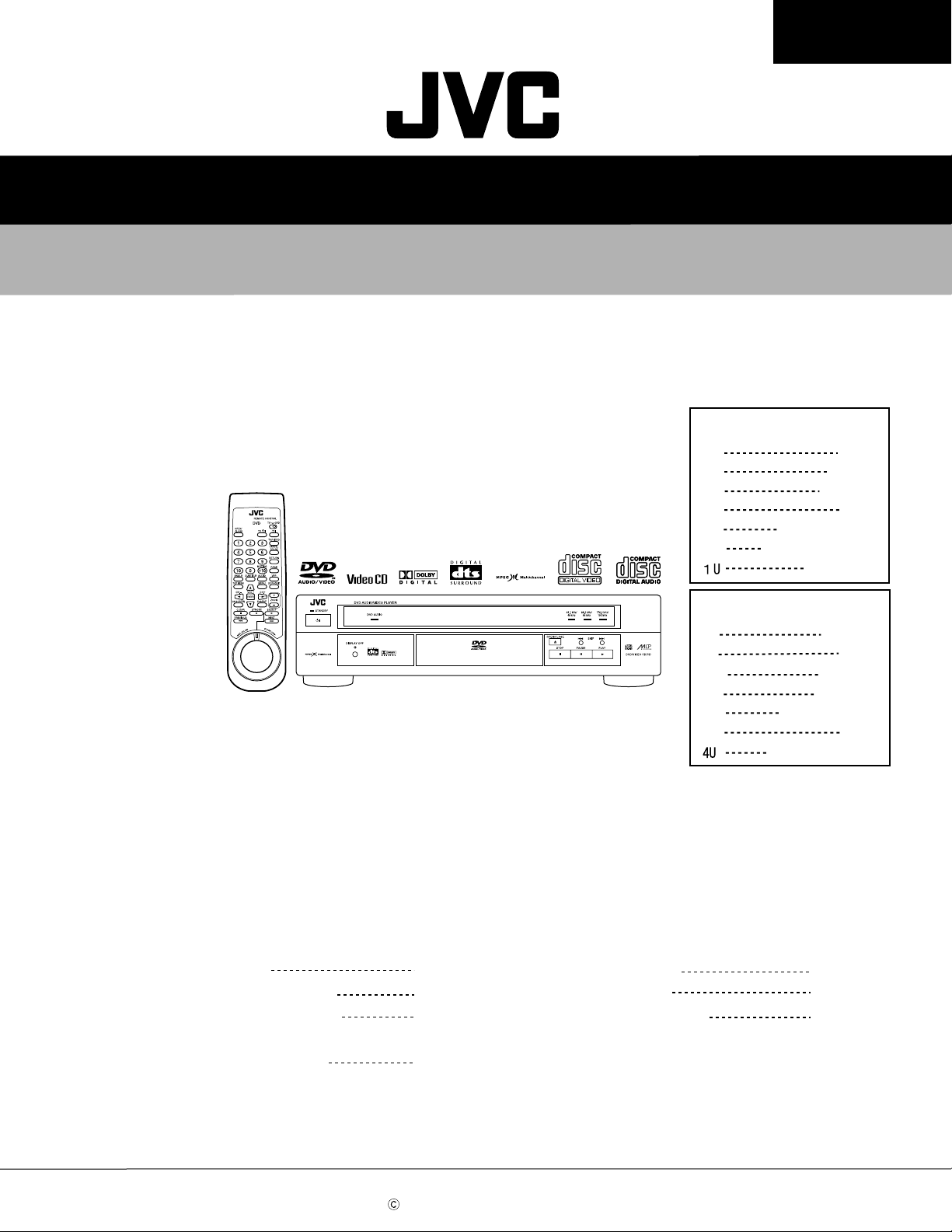
DVD AUDIO/VIDEO PLAYER
XV-D721BK
XV-D721BK
XV-D721BK
XV-D723GD
XV-D723GD
XV-D723GD
Area Suffix
XV-D721BK
J
C
EG
ES
EN
EE
Area Suffix
XV-D723GD
A
J
EG
ES
EN
UF
U.S.A
Canada
Germany
Spain
Northern Europe
Russian Federation
US Minitary
Australia
U.S.A
Germany
Singapore
Northern Europe
China
Brazil,Mexico,Peru
Contents
Safety Precautions
Preventing static electricity
Important for laser products
Importance Admistering
point on the Safety
This service manual is printed on 100% recycled paper.
COPYRIGHT 2000 VICTOR COMPANY OF JAPAN, LTD.
1-2
1-3
1-4
1-5
Disassembly method
Adjustment method
Description of major ICs
1-6
1-11
1-18
No.A0002
Nov. 2000
1-1
Page 2
XV-D721BK
XV-D723GD
1. This design of this product contains special hardware and many circuits and components specially
for safety purposes. For continued protection, no changes should be made to the original design
unless authorized in writing by the manufacturer. Replacement parts must be identical to those
used in the original circuits. Services should be performed by qualified personnel only.
2. Alter ations of the design or circuitry of the product should not be made. Any design alterations of
the product should not be made. Any design alterations or additions will void the manufacturer`s
warranty and will further relieve the manufacture of responsibility for personal injury or proper ty
damage resulting therefrom.
3. Many electrical and mechanical par ts in the products have special safety-related characteristics.
These characteristics are often not evident from visual inspection nor can the protection afforded
by them necessarily be obtained by using replacement components rated for higher voltage,
wattage, etc. Replacement par ts which have these special safety characteristics are identified in
the Parts List of Service Manual. Electrical components having such features are identified by
shading on the schematics and by ( ) on the Parts List in the Service Manual. The use of a
substitute replacement which does not have the same safety characteristics as the recommended
replacement parts shown in the Parts List of Service Manual may create shock, fire, or other
hazards.
4. The leads in the products are routed and dressed with ties, clamps, tubings, barriers and the
like to be separated from live parts, high temperature parts, moving parts and/or sharp edges
for the prevention of electric shock and fire hazard. When ser vice is required, the or iginal lead
routing and dress should be observed, and it should be confirmed that they have been returned
to normal, after re-assembling.
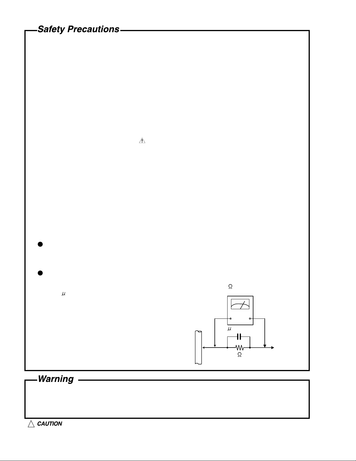
5. Leakage currnet check (Electrical shock hazard testing)
After re-assembling the product, always perform an isolation check on the exposed metal parts
of the product (antenna terminals, knobs, metal cabinet, screw heads, headphone jack, control
shafts, etc.) to be sure the product is safe to operate without danger of electrical shock.
Do not use a line isolation transformer during this check.
Plug the AC line cord directly into the AC outlet. Using a "Leakage Current Tester", measure
the leakage current from each exposed metal parts of the cabinet , particularly any exposed
metal part having a return path to the chassis, to a known good earth ground. Any leakage
current must not exceed 0.5mA AC (r.m.s.)
Alternate check method
Plug the AC line cord directly into the AC outlet. Use an AC voltmeter having, 1,000 ohms
per volt or more sensitivity in the following manner. Connect a 1,500 10W resistor paralleled by
a 0.15 F AC-type capacitor between an exposed
metal part and a known good earth ground.
Measure the AC voltage across the resistor with the
AC voltmeter.
AC VOLTMETER
(Having 1000
ohms/volts,
or more sensitivity)
Move the resistor connection to eachexposed metal
part, par ticularly any exposed metal part having a
return path to the chassis, and meausre the AC
voltage across the resistor. Now, reverse the plug in
the AC outlet and repeat each measurement. voltage
measured Any must not exceed 0.75 V AC (r.m.s.).
0.15 F AC TYPE
1500 10W
Place this
probe on
each exposed
metal part.
This corresponds to 0.5 mA AC (r.m.s.).
Good earth ground
1-2
1. This equipment has been designed and manufactured to meet international safety standards.
2. It is the legal responsibility of the repairer to ensure that these safety standards are maintained.
3. Repairs must be made in accordance with the relevant safety standards.
4. It is essential that safety critical components are replaced by approved parts.
5. If mains voltage selector is provided, check setting for local voltage.
!
Burrs formed during molding may be left over on some parts of the chassis. Therefore,
pay attention to such burrs in the case of preforming repair of this system.
Page 3
XV-D721BK
XV-D723GD
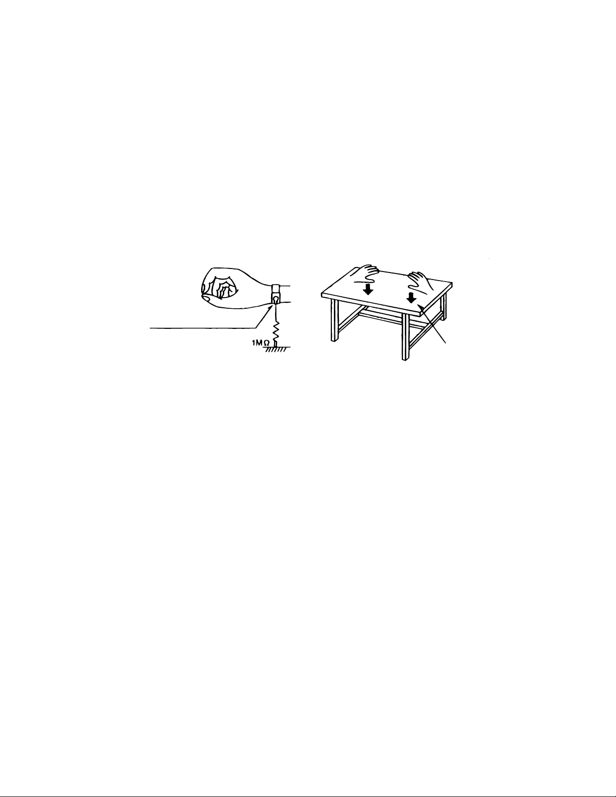
Preventing static electricity
Electrostatic discharge (ESD), which occurs when static electricity stored in the body, fabric, etc. is discharged,
can destroy the laser diode in the traverse unit (optical pickup). Take care to prevent this when performing repairs.
1.1. Grounding to prevent damage by static electricity
Static electricity in the work area can destroy the optical pickup (laser diode) in devices such as DVD players.
Be careful to use proper grounding in the area where repairs are being performed.
1.1.1. Ground the workbench
1. Ground the workbench by laying conductive material (such as a conductive sheet) or an iron plate over
it before placing the traverse unit (optical pickup) on it.
1.1.2. Ground yourself
1. Use an anti-static wrist strap to release any static electricity built up in your body.
(caption)
Anti-static wrist strap
Conductive material
(conductive sheet) or iron plate
1.1.3. Handling the optical pickup
1. In order to maintain quality during transport and before installation, both sides of the laser diode on the
replacement optical pickup are shorted. After replacement, return the shorted parts to their original condition.
(Refer to the text.)
2. Do not use a tester to check the condition of the laser diode in the optical pickup. The tester's internal power
source can easily destroy the laser diode.
1.2. Handling the traverse unit (optical pickup)
1. Do not subject the traverse unit (optical pickup) to strong shocks, as it is a sensitive, complex unit.
2. Cut off the shorted part of the flexible cable using nippers, etc. after replacing the optical pickup. For specific
details, refer to the replacement procedure in the text. Remove the anti-static pin when replacing the traverse
unit. Be careful not to take too long a time when attaching it to the connector.
3. Handle the flexible cable carefully as it may break when subjected to strong force.
4. It is not possible to adjust the semi-fixed resistor that adjusts the laser power. Do not turn it
1-3
Page 4
XV-D721BK
XV-D723GD
Important for Laser Products
1.CLASS 1 LASER PRODUCT
2.DANGER : Invisible laser radiation when open and inter
lock failed or defeated. Avoid direct exposure to beam.
3.CAUTION : There are no serviceable parts inside the
Laser Unit. Do not disassemble the Laser Unit. Replace
the complete Laser Unit if it malfunctions.
4.CAUTION : The compact disc player uses invisible
laserradiation and is equipped with safety switches
whichprevent emission of radiation when the drawer is
open and the safety interlocks have failed or are de
feated. It is dangerous to defeat the safety switches.
5.CAUTION : If safety switches malfunction, the laser is able
to function.
6.CAUTION : Use of controls, adjustments or performance of
procedures other than those specified herein may result in
hazardous radiation exposure.
!
Please use enough caution not to
see the beam directly or touch it
in case of an adjustment or operation
check.
REPRODUCTION AND POSITION OF LABELS
WARNING LABEL
CLASS 1
LASER PRODUCT
REAR
FRONT CENTER
LEFT
LEFT
RIGHT
RIGHT
ANALOG
PCM/STREAM
DIGITAL
COAXIAL
OPTICAL
AUDIO OUT AV COMPU LINK
SUBWOOFER
VIDEO S-VIDEO
YPBP
COMPONENT
VIDEO OUT
SCAN MODE
R
525p 525i
CLASS 1
LASER PRODUCT
1
AC IN
CAUTION - - LASER RADIATION WHEN OPEN.
DO NOT STARE INTO BEAM.
ATTENTION RAYONNEMENT LASER EN CAS D’OUVERTURE.
NE PAS REGARDER DANS LE FAISCEAU.
- VORSICHT LASERSTRAHLUNG, WENN ABDECKUNG GEÖFFENET.
NICHT IN DEN STRAHL BLICKEN.
- ADVARSEL LASERSTRÅ LING VED Å BNING.
SE IKKE IND I STRÅ LEN.
- ADVARSEL LASERSTRÅ LING NÅ R DEKSEL Å PNES.
STIRR IKKE INN I STRÅ LEN.
-
VARNING LASERSTRÅ LNING NÄR DENNA DEL ÄR ÖPPNAD.
STRRA EJ IN I STRÅ LEN.
VARO! AVATTAESSA OLET ALTTIINA LASERSÄTEILYLLE.
ÄLÄ TUIJOTA SÄTEESEEN.
-
-
1-4
Page 5
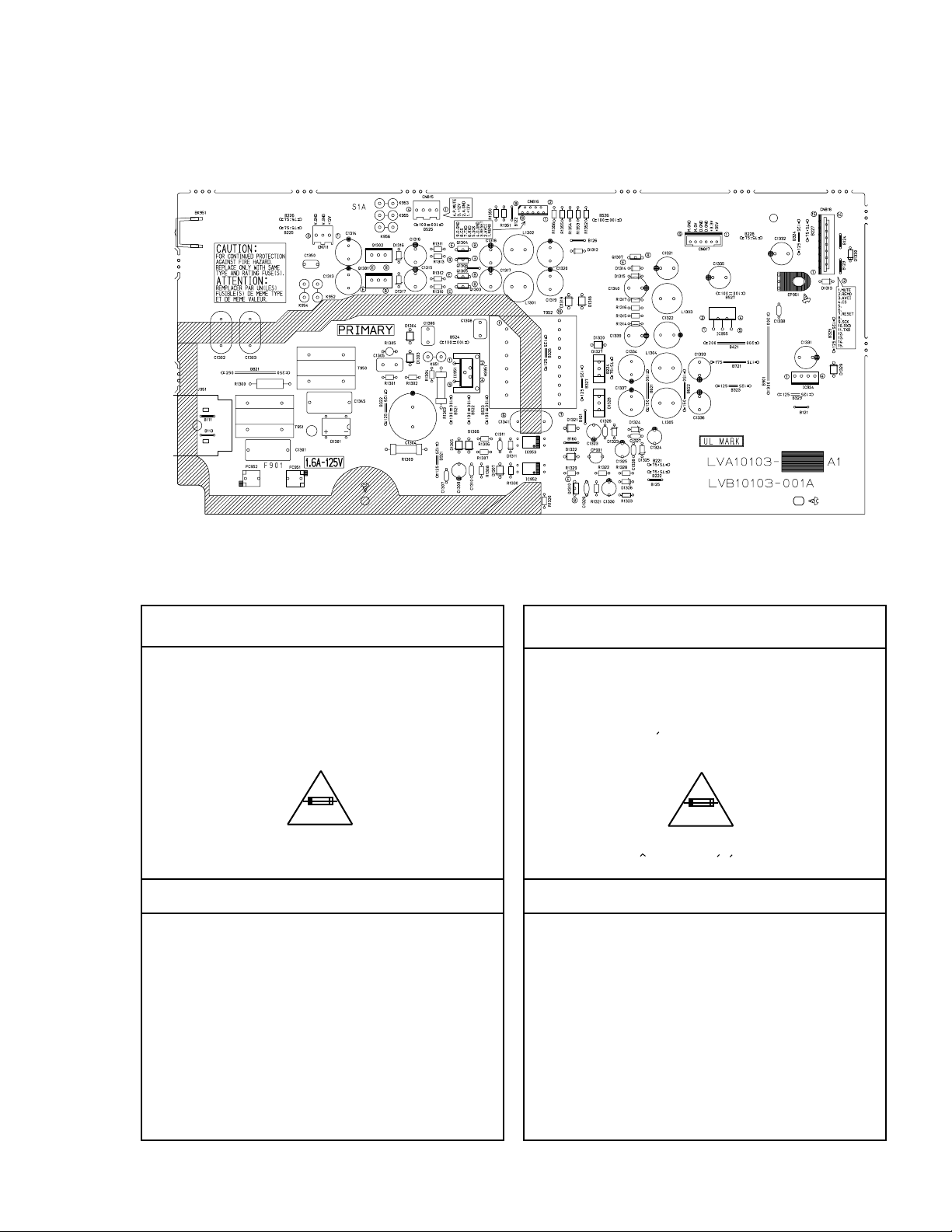
Importance Admistering point on the Safety
XV-D721BK
XV-D723GD
Note : It's means "J" for U.S.A. market model and "C" for canada market model.
XV-D721BK/XV-D723GD C/J ONLY
Full Fuse Replacement Marking
Graphic symbol mark
(This symbol means fast blow type fuse.)
should be read as follows ;
FUSE CAUTION
FOR CONTINUED PROTECTION AGAINST RISK
OF FIRE, REPLACE ONLY WITH SAME TYPE
AND RATING OF FUSES ;
F901 : 1.6 A / 125 V
XV-721BK/XV-723GD C/J SEULEMENT
Marquage Pour Le Remplacement
Complet De Fusible
Le symbole graphique (Ce symbole signifie
fusible de type a fusion rapide.)
doit etre interprete comme suit ;
PRECAUTIONS SUR LES FUSIBLES
POUR UNE PROTECTION CONTINUE CONTRE
DES RISQUES D'INCENDIE, REMPLACER
SEULEMENT PAR UN FUSIBLE DU MEME TYPE ;
F901 : 1.6 A / 125 V
1-5
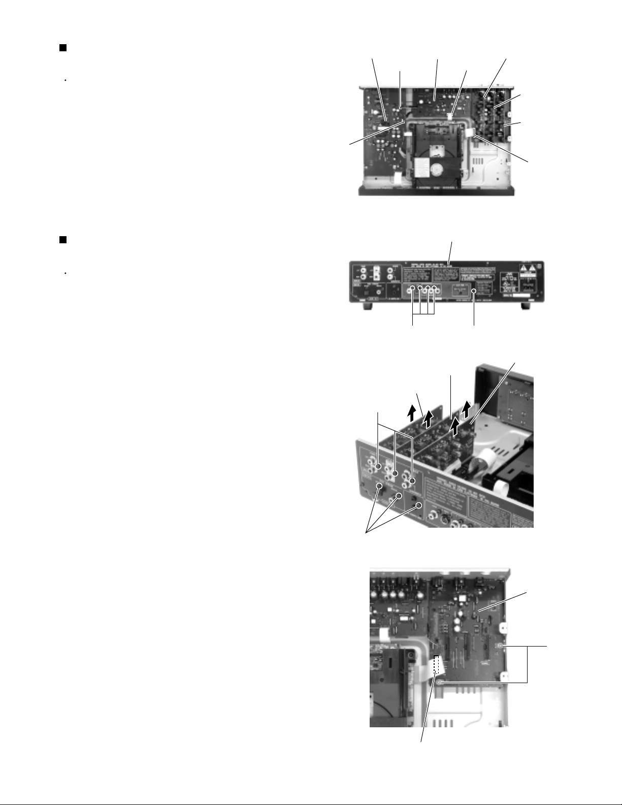
Page 6
XV-D721BK
XV-D723GD
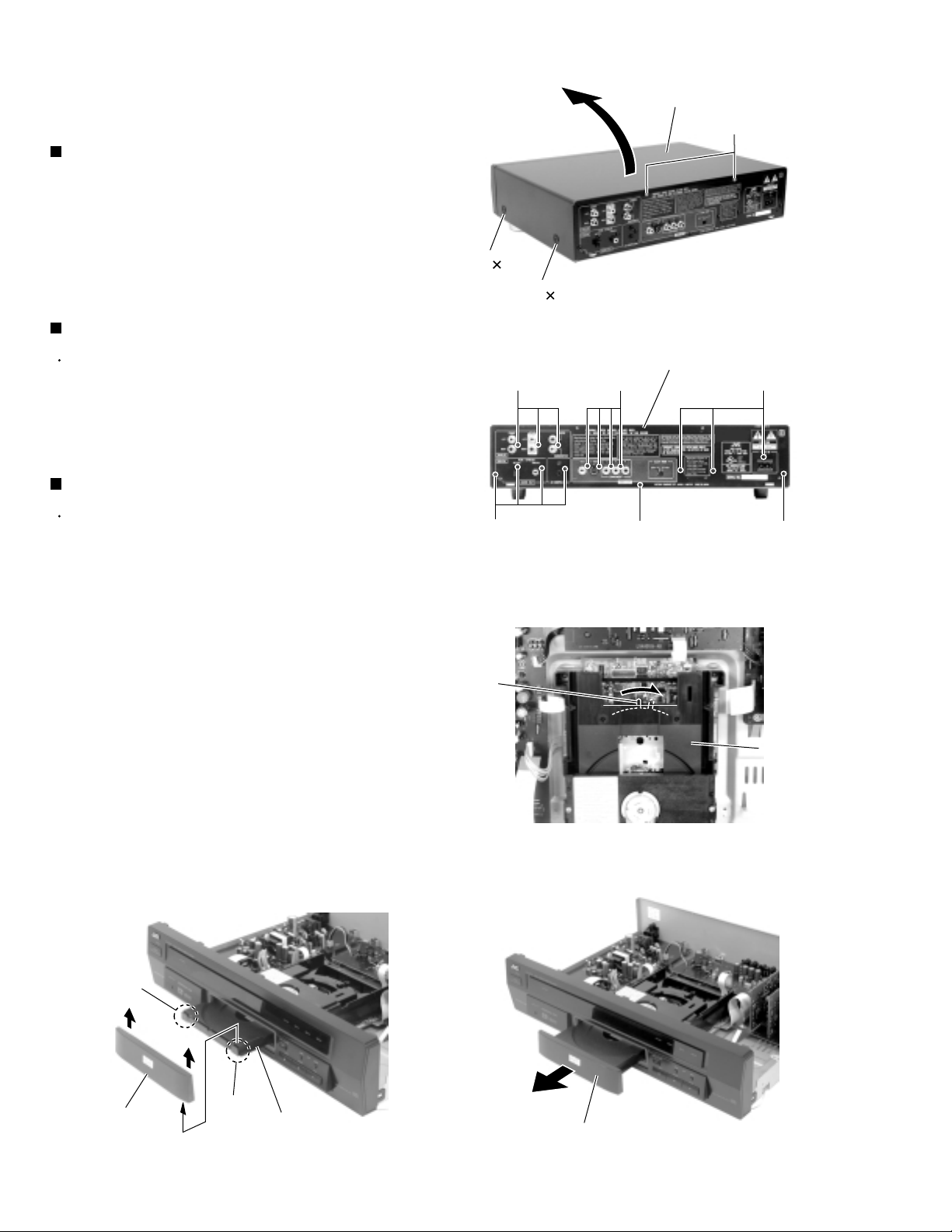
Disassembly method
< Main body>
Removing the top cover (See Fig.1)
1.
Remove the four screws A on each side of the body.
2.
Remove the two screws B on the back of the body.
3.
Remove the top cover from behind in the direction of
the arrow while pulling the lower part of the sides.
Removing the rear panel (See Fig.2)
A
2
A 2
Top cover
B
Fig.1
Prior to performing the following procedure, remove
the top cover.
1.
Remove the sixteen screws C on the back of the
body.
Removing the fitting (See Fig.3 to 5)
Prior to performing the following procedure, remove
the top cover.
ATTENTION:
1.
Lower the mechanism by moving the lever marked a
in the direction of the arrow from the upside of the
body (Refer to Fig.3).
2.
Manually eject the loading tray toward the front.
3.
Remove the fitting from the loading tray by releasing
the joints b on the both sides of the fitting.
4.
Push and return the loading tray.
To remove the front panel assembly and
the DVD mechanism assembly, remove
the fitting in advance.
Lever a
CC
CC
Fig.2
Rear panel
C
C
Loading tray
1-6
Joint b
Fitting
Joint b
Loading tray
Fig.3
Loading tray
Fig.4Fig.5
Page 7
XV-D721BK
XV-D723GD
Removing the front panel assembly
(See Fig.6 to 9)
Prior to performing the following procedure, remove
the top cover and the fitting.
1.
Disconnect the card wire from connector CN818 on
the regulator board.
2.
Turn back the body and remove the three screws D
fixing the front panel assembly.
3.
Release the two joints c on both sides of the body
and remove the front panel assembly toward the
front.
Regulator board
CN818
Front panel assembly
Fig.6
DD
Front panel assembly
(Bottom)
Fig.7
Fig.8
Joint c
Joint c
Fig.9
1-7
Page 8
XV-D721BK
XV-D723GD
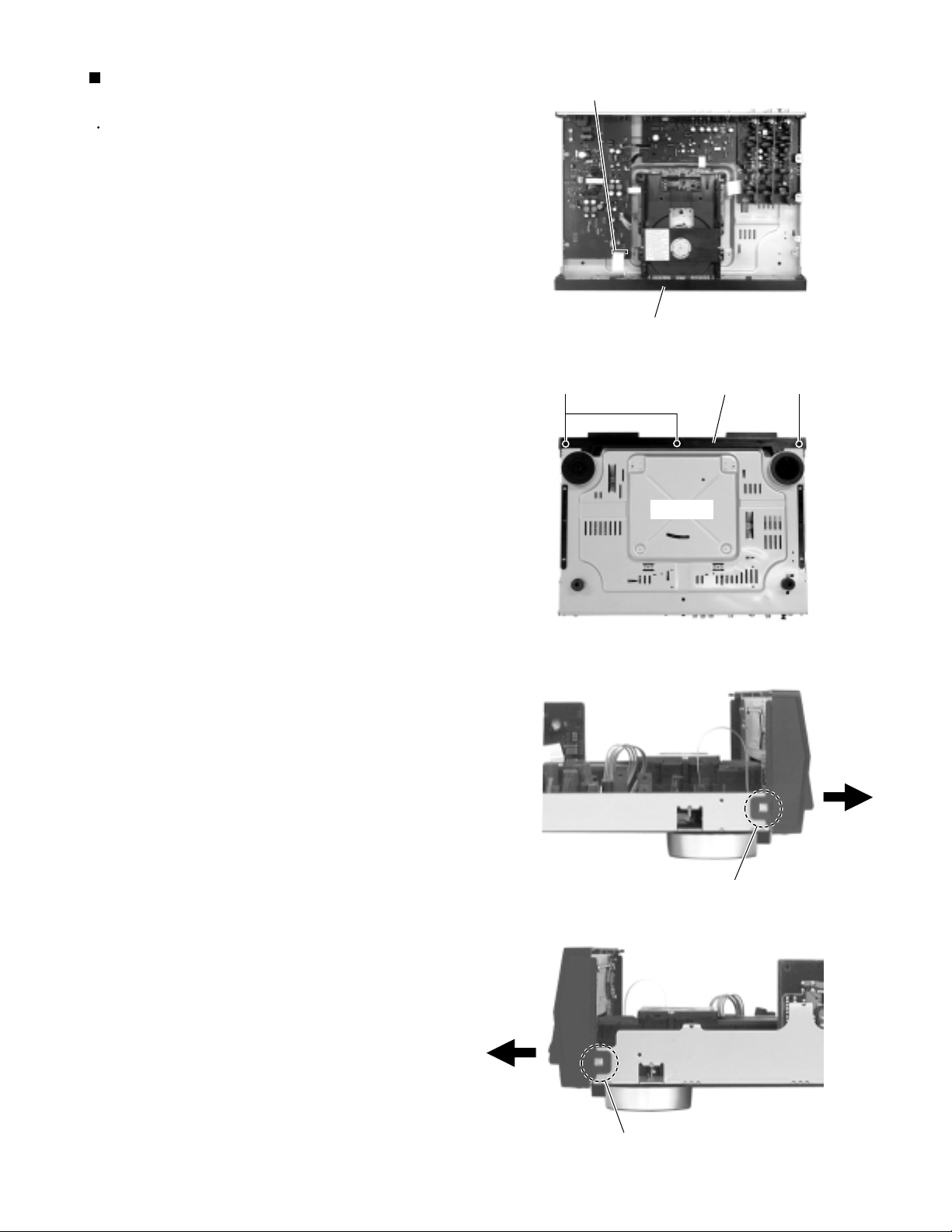
Removing the DVD mechanism
(See Fig.10)
Prior to performing the following procedure, remove
the top cover and the fitting.
It is not necessary to remove the front panel
assembly.
1.
Disconnect the card wire from connector CN816 and
the harness from CN817 on the regulator board.
2.
Disconnect the card wire from connector CN701 on
the video board.
3.
Disconnect the card wire from CN831 on the DSP
board.
4.
Remove the four screws E and the DVD mechanism
assembly by pulling out from the front panel
assembly backward.
Removing the regulator board
(See Fig.11 and 12)
Regulator board
CN816
CN817
Regulator board
Video board
CN701
E
E
DVD mechanism assembly
Fig.10
CN711 CN815
E
E
DSP board
CN831
Prior to performing the following procedure, remove
the top cover.
It is not necessary to remove the rear panel.
1.
Disconnect the card wire from connector CN816 and
CN818 and the harnesses from CN815,CN817 and
CN711 on the regulator board.
2.
Remove the three screws F attaching the regulator
board.
3.
Remove the two screws C on the rear panel.
F
CN816
CN817
F
F
CN818
Rear panel
Fig.11
CC
Fig.12
1-8
Page 9
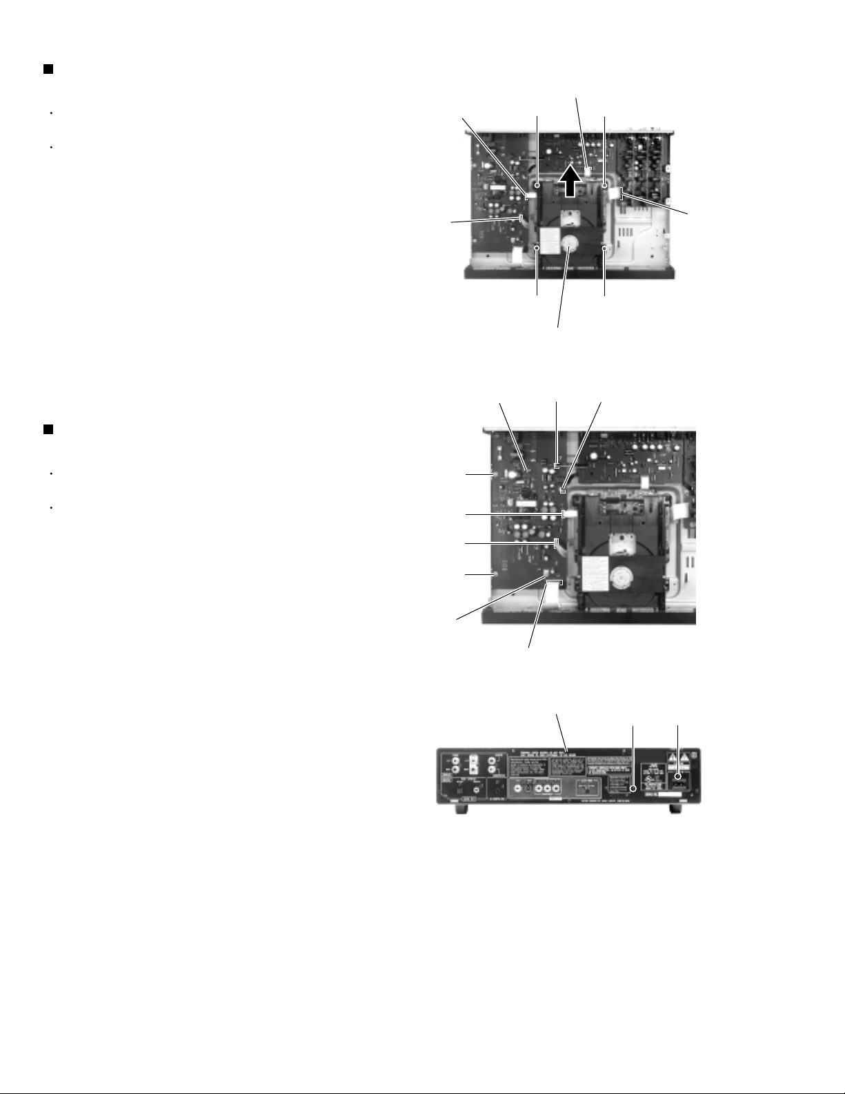
XV-D721BK
XV-D723GD
Removing the video board
(See Fig.13 and 14)
Prior to performing the following procedure, remove
the top cover.
Ref. :
It is not necessary to remove the rear panel.
1.
Disconnect the harnesses from the connector CN711
on the regulator board.
2.
Disconnect the card wire from connector CN701 on
the video board.
3.
Remove the five screws C on the rear panel.
Removing the Audio board 1,2 and 3 / the
Audio board (See Fig.13,15 and 16)
Prior to performing the following procedure, remove
the top cover and rear panel.
1.
Remove the three screws C attaching the audio
board 1,2 and 3.
Regulator board
CN815
CN711
C
Video board
Fig.13
Rear panel
Fig.14
Audio board 3
CN701
Audio board 2
Audio board 1
Audio board
CN831
C
2.
Disconnect the audio board 1,2 and 3 from the audio
board respectively.
3.
Disconnect the harnesses from connector CN815 on
the regulator board.
4.
Disconnect the card wire from connector CN831 on
the audio board.
5.
Remove the two screws G attaching the audio
board.
Audio board 1
C
C
Audio board 3
Audio board 2
Fig.15
Audio board
G
CN831
Fig.16
1-9
Page 10
XV-D721BK
XV-D723GD
Removing the DVD servo board
(See Fig.17)
Prior to performing the following procedure, remove
the top cover and the DVD mechanism assembly.
1.
Turn over the DVD mechanism assembly and
disconnect the card wire from connector CN102 and
CN103 on the DVD servo board.
2.
Remove the two screws H attaching the DVD servo
board. Move the DVD servo board in the direction of
the arrow to release the two corner joints d.
DVD mechanism board
CN103
H
Joint d Joint d
DVD servo board
Fig.17
CN102
H
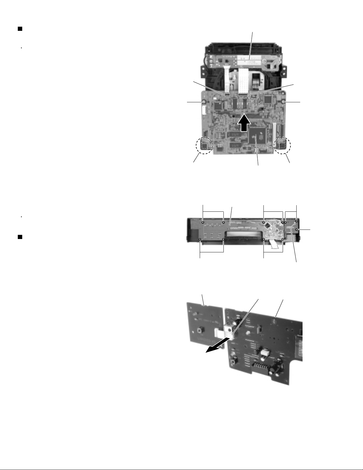
<Front panel assembly>
Prior to performing the following procedure, remove
the top cover and the front panel assembly.
Removing the FL board / the power
switch board (See Fig.18 and 19)
1.
Remove the eight screws I and three screws J on
the back of the front panel assembly. Remove the FL
board and the power switch board at the same time.
Disconnect the harness from connector CN903 on
2.
the FL board.
FL board
II
Power switch board
Fig.18
II
Power switch board
CN903 FL board
J
J
1-10
Fig.19
Page 11
XV-D721BK
XV-D723GD
Adjustment method
This model has the TEST mode for simple diagnosis of the internal function. Use the TEST mode for diagnosing and checking
the set as mentioned below.
Details of the TEST mode
The TEST mode comprises the five modes of the following.
FL indication (*: numeral)
1.DVD AUDIO copyright protection key serial indication
Indicates the content of the DVD AUDIO copyright at shipment. Use this mode for checking it.
2.Microcomputer's version number indication
Indicates the initial version number of the microcomputer at shipment. Use this mode for checking it.
3.Servo signal system check mode CHECK
Use this mode for checking the laser pickup status.
4.Indication check mode The FL and LED's go on in full.
The LED's and FL of the set go on in full. Use this mode for checking indications.
5.Microcomputer software upgrading mode UPGRADE
Use this mode for upgrading the microcomputer software.
How to set the TEST mode
1.While pressing the STOP key and PLAY key of the set together, plug in the power cord.
*Continue to pressing both the STOP key and PLAY key until reading of disk data completes (until the "NOW READING"
message changes into a DVD logo).
2."TEST *" message appears on the FL. (* In the part of the sign, the sign is different according to the destination.)
3.The five modes of the TEST mode change one after another each time the DISPLAY OFF key of the set is pressed.
4.To recover the usual operation mode, turn off the set by pressing the POWER ON/OFF key.
********
**_**_**
How to check the laser pickup
Since the laser pickup of the set is easily affected by static electricity, heat, etc., it may be damaged depending on use
condition. If the set shows such a symptom as it fails in reading disk data, check the laser pickup as follows.
* Checking laser current
1.Enter the set into the "servo signal system check mode" of the TEST mode.
2.Press the SKIP | key of the set.
The laser is turned on and the LAS **** message appears on the FL display. **** in the message indicates the current
in code. For knowing the actual laser current, read the first two figures (omitting the last two figures) and convert the
number into the current (mA) referring to the following conversion table, because the FL indication is a hexadecimal
number. Since the FL indication varies because of self-heating of the set, read the indication value about 20 seconds
after the set was turned on. If the indicated value is the OK level (see the conversion table), the laser is judged to be
normal in the initial status by this simple checking method.
3. Press the STOP key to set back the check mode to the initial status.
Laser current conversion table
FL indication
Current (mA)
Judgment
FL indication
Current (mA)
Judgment
FL indication
Current (mA)
Judgment
1-11
Page 12

XV-D721BK
XV-D723GD
* Automatic adjustment/Jitter value indication
1.Enter the set into the "servo signal system check mode" of the TEST mode.
2.Open the tray with the OPEN key of the set. Set the TEST disk VT-501 on the tray and put back the tray with
the CLOSE key. Then, press the PAUSE key.
The TEST disk starts rotation to execute automatic adjustment. If the set is in the normal condition, the
"CHECK OK" message appears. If there is something abnormal in the adjustment values, an error message
appears and it mostly comes from a failure in the servo system (including the mechanism and pickup). In
such the event, refer to the check points by errors.
When using the TEST disk VT-501, carefully check to see if there is neither damage nor dirt on the read
surface of the disk beforehand.
3.Press the STOP key to return the check mode to the initial status.
4.After the automatic adjustment with the TEST disk completes, press the PLAY key.
The disk starts rotation and a jitter value (signal read precision in percentage) appears on the FL display (JIT
0***). If the indication value (in *** places) is 110 (11 %) or less, it can be judged by this simple checking
method that the signal read precision of the set is satisfactory.
Before using the TEST disk VT-501, carefully check it if there is neither damage nor dirt on the read surface.
5.Press the STOP key to return the mode to the initial status.
Upgrading microcomputer software
The internally incorporated microcomputer software of this set can be revised in part for the reason that the set
is designed to conform to new standards and to be capable of playing disks to be put on the market by other
manufacturers. To upgrade the internal microcomputer software, use the upgrade disk and follow the procedure
mentioned below.
* How to upgrade the microcomputer software
1.Set the upgrade disk in the set and enter it into the TEST mode.
2.After confirming that the set completes reading of the upgrade disk data while looking at the indication on the
monitor screen, change the TEST mode to the microcomputer software upgrading mode and then press the
PLAY key.
3.The set completes writing of the upgrade disk data approximately 1 minute later and it is automatically reset
by the self-resetting function. Then the set again reads the upgrade disk and stops automatically.
4.Take the upgrade disk out of the set and turn it off with the POWER ON/OFF key.
5.Again enter the set into the TEST mode, and press the SKIP key and then the PAUSE key.
6.Make sure that the DVD AUDIO indicator goes on a few seconds after the above-mentioned operation, check
the version number of the microcomputer software in the microcomputer software version number indication
mode.
*Carefully carry out the above procedure. If data write is interrupted in the middle of course by power failure
or careless shutdown operation, not only the data of the internal software may be damaged but the set may
fail in resetting. The version number of the internal microcomputer software is shown as follows.
FL indication: ** ** **
[IC901] [IC401] [IC508/IC509] Symbol number of microcomputer IC
Initializing the set
Initialization of the set returns it to the initial status at shipment.
Be sure to initialize the set after repair service.
* How to initialize the set
1.Enter the set into the TEST mode and press the SKIP key first and the PAUSE key second.
2.Make sure that the DVD AUDIO indicator goes on a few seconds later.
DVD AUDIO copyright protection
To protect the DVD AUDIO copyright from infringement, a number proper to each DVD AUDIO set called a
device key is assigned to each set. If a proper device key is not set for a set, it fails in playing a copyrighted
disk.
The management number of the device key of a set can be checked by the DVD AUDIO copyright protection
key serial indication in the TEST mode. If the "???...." message appears in this check mode, the set has a
failure in the device key. If it occurs, inquire at the Service Section of the Audio and Communication Division,
JVC.
1-12
Page 13

Check points for each error
(1) Spindle start error
*Defective spindle motor
Are there 10ohms resistance between each pin of CN102 "1~4"?
(The power supply is turned off and measured.)
*Hall element: Is sine wave output between CN102 "10" and "11", between "12" and "13",
and between "14" and "15" during rotation?
In either case, replace the mechanical unit.
*Defective spindle driver (IC251)
Is a driving wave output from CN102 "1~4" ?
During
rotation
Is IC251 "9" at "H" level (START)?
Servo IC --- Is control signal sent to the motor driver ?
IC201 "95" : Duty is 50% during stop, but varies during rotation (greatly varies at start).
--- If not sent, pattern or servo IC (IC201) is defective.
XV-D721BK
XV-D723GD
R259 : approx 2.5V during stop, but varies during rotation (greatly varies at start).
--- of not sent, pattern or servo IC (IC201) is defective.
Is FG input to servo IC ?
Observe FG wave from IC201 "89". --- If not output, pattern, IC251 or IC201 is defective.
(2) Disc Detection, Distinction error (no disc, no REFNV)
* Laser is defective.
* Front End Processor is defective (IC101).
* APC circuit is defective. --- Q101.
* Pattern is defective. --- Lines for CN101 "15" and "17".
Lines for between IC201 "2" and IC101 "2"(LDONA),
between IC201 "3" and IC101 "1" (LDONB).
* Servo IC is defective (IC201).
* Is signal sent to IC201(servo)"71" AS2 ?
* IC101 --- For signal from IC101 to IC301, is signal output from IC101 "88" (RFAS1) and
IC101 "69" REENV ?
1-13
Page 14

XV-D721BK
XV-D723GD
(3) Traverse movement NG
* For automatic adjustment, traverse movement occurs only when the position is changed to retry
judging the disc type after the 1st judgment resulted in an error. Therefore, traverse movement
rarely occurs because, in most cases, disc judgment at the current position (1st time judgment)
is executed successfully. (Of course, NG rarely occurs in this step.)
Note: 1st time judgment of disc type resulted in NG. --- The re-judgment of disc type may not be
successful. Therefore, after removing the cause of traverse movement, re-execute automatic
adjustment and confirm that no problem exists.
* Check point
a) During stop
Whether 50% duty pulse is output to R273
Whether between R274 and C271 is at approx. 2.5VDC
Offset voltage between CN102 "1" and "2" (scores mV if exists)
b) When tray is opened or closed
Check by oscilloscope whether a rectangular wave signal is output from CN102 "1" or "2".
50msec
2.5V
Approx.
500mV
GND
If checking a) or b) resulted in NG, IC201 maybe defective.
(4) Focus ON NG
* Is FE output ? --- Pattern, IC101
* Is FCDRV signal sent ? (R286) --- Pattern, IC301
* Is driving voltage sent ?
CN101 "1", "3" --- If NG, pattern, driver, mechanical unit (with the power turned off, measure the
resistance between CN101 "20" and "21").
* Does CN101 "8" become "H" and is the focus drawing in done?
--- Mechanical unit (laser power too low), IC101(defective gain)
--- Moreover, It is thought that abnormality is found in the disk.
* Mechanical unit is defective.
(5) Tracking ON NG
* When the tracking loop cannot be drawn in, IC201 "58" (/TRON) does not become "L".
* Mechanical unit is defective.
Because the undermentioned adjustment value is abnormal, it is not possible to draw in normally.
* Periphery of driver (IC271)
Constant or IC it self is defective.
(When passing without becoming abnormal while adjusting the following.)
* Servo IC (IC201)
When improperly adjusted due to defective IC.
1-14
[Focus position rough adjustment]
[Phase difference cancellation rough adjustment]
[Tracking balance adjustment]
Page 15

XV-D721BK
XV-D723GD
(6) Spindle CLV NG
* When the spindle cannot be shifted to CLV Servo, does not become "H" between IC201 "18"
and IC301"88".
* IC201 Is signal output from IC101 "87" (RFOP)?
* IC201 Is signal output from IC201 "60" to "64" (binary-coded clock and data)?
* IC201 Is "58" (/TRON) at "L" level ?
* IC301 "74" to "76" --- Is signal output to IC201 "24", "25", "28" (In case of only CD).
(Serial communication of rotation information)
* Spindle motor driver is defective.
Even when one of the three phases is defective, item (1) may be passed.
--- Check the second item in (1) above.
* C260 to C263 Defective soldering
If noise eliminating capacitors are not properly soldered, noise may ride on the waveform.
* Besides, the undermentioned cause is thought though specific of the cause is difficult because various
factors are thought.
Mechanism is defective.(jitter)
IC101, IC201.
(7) Address read NG
* Besides, the undermentioned cause is thought though specific of the cause is difficult because various
factors are thought.
Mechanism is defective. (jitter)
IC201, IC301, IC401.
The disc is dirty or the wound has adhered.
(8) Between layers jump NG (double-layer disc only)
* When the focus flight is generated when jumps between layers.
Because all adjustments for L1 layer must be successful, this error may rarely be due to a
circuit defect.
* Crosstalk might occur from tracking to focus system. (See (11) ) --- Replace the mechanical unit.
* Driver surroundings.
* Defect of constant and IC.
* For double-layer discs, after checking CLV on layer L1, jumps to layer L0 after mode changes to FG.
Then tracking is turned off, and adjustments are executed from the focus position coarse adjustment
in order.
* When the jump between layers is done on the single-layer disk, the disk distinction error is thought.
--- The laser power is low (RF level is confirmed by IC101"87" (RFOP)).
--- AS1, AS2, REFNV Is the signal sent to between IC101 and IC201 ?
1-15
Page 16

XV-D721BK
XV-D723GD
(9) Neither picture nor sound is output
* Cannot search
a) Can the feed system be driven?
Check the waveform of TRSDRV signal (R273). --- Waveform between R274 and C271.
Search results in a change of duty
(three values with 2.5V at the center)
(The figure is exaggerated.)
Check the waveform of CN101 "1" and "2". --- After the driver (IC271)
b) Is kick available?
Check the TRDRV signal waveform from R289.
Check the waveform of CN101 "2" and "4" --- After the driver (IC271)
Although differs in amplitude and DC offset, the waveform is similar to that of R289
Kick pulse
Approx.
2.5V
Long-distance seek
Acceleration pulse at start;
deceleration pulse at stop
(each one)
(In the direction of search,
opposite to this figure)
For short-distance search, the waveform
becomes roundish, not trapezoidal, and
voltage is low.
Feed
Tracking
Kick pulse (fine seek) is
inserted after longdistance seek.
(Not one)
1-16
Hold (DC) during feed
Page 17

(10) Picture is distorted or abnormal sound occurs at intervals of several seconds.
XV-D721BK
XV-D723GD
Does JITOUT
change periodically?
(2V or more in peak
value, except
during kick)
YES
Feed system is defective (drive gain is defective: too large).
Check the waveform according to a) in (9).
Play back a simple disc with no angle change.
OK when the following waveform appears at intervals
of several seconds.
5~10Sec.
1~1.2V
Some system other
NO
than servo may be
defective.
If this voltage is too
high (2V or more, for
example), feed motor
may be defective, or
the mechanical unit
has seized.
(11) Others (unusual events experienced to date)
* Problem occurs with double-layer discs although no problem occurs with single-layer DVD.
(Error occurs, or search becomes unstable and takes longer.)
Crosstalk might occur from tracking to focus system.
--- When FE was observed during search (skip, etc.), it was found that a wave resembling TE
with an amplitude of 200mVp-p was riding on FE.
--- Mechanical unit was replaced.
* Error frequently occurred in the outer part of discs although no error occurred in the inner part.
--- Mechanical unit was replaced because tilt seemed to be defective.
(12) CD During normal playback operation
a) Is TOC reading normal?
NO
Please refer to "Servo Volume" flow.
Displays total time
for CD-DA.
Shifts to double-speed
mode for V-CD.
YES
b)Playback possible?
NO
*--:-- is displayed during FL serch.
According to [*Cannot serch ] for DVD(9), check the feed
and tracking systems.
*No sound is output although the time is displayed.(CA-DA)
*DAC, etc, other than servo.
*The passage of time is not stable, or picture is abnormal.(V-CD)
*The wound of the disc and dirt are confirmed.
(13) Others
V-CD : Frequent occurrence of error in inside and outer.
(Even the disk without the wound : when generated.)
Waveform observation
--- Is the oscillation frequency of about 700~900Hz output?
(Borrow a pertinent disk for the complaint for the combination with the disk.)
--- Exchanges mechanism for the mechanism resonance.
1-17
Page 18

XV-D721BK
XV-D723GD
Description of major ICs
AN8706FHQ (IC101) : Front end processor
1.Pin layout
CBDOSL
CSAG
DCAGC
AGCG
PEAK
BOTTOM
RFENVFCBOOST
OFTR
BDO
75747372717069686766656463626160595857565554535251
RBCA
RFINP
RFINN
VCC2
GND2
VREF2
RFON
RFOP
TS
DCRF
FS
VIN6
VIN5
VCC1
VIN1
VIN2
VIN3
VIN4
VREF4
DIFP
DIFN
76
77
78
79
80
81
82
83
84
85
86
87
88
89
90
91
92
93
94
95
96
97
98
99
100
AN8706FHQ
CBDOFS
TESTSG
COFTFS
COFTSL
JITOUT
GND3
FUPDN
ITDLI
VCOIN
PLFLT
PLFLT2
FCPO
PCPO
VCC3
CAPA
DTRD
IDGT
VCC5
50
RDCKP
49
RDCKN
48
RDTP
47
RDTN
46
GND5
45
GND4
44
VCC4
43
DTMONN
42
DTMONP
41
DSLFLT
40
DSLO
39
FLTOUT
38
DCFLT
37
VREF3
36
VPWBDO
35
VPWOFT
34
IDDLY
33
DBAL
32
GND1
31
VREF1
30
TKCNT
29
TKCFLT
28
TEOUT
27
TEI
26
RSCL
2.Block diagram
Head Amp.
SSD Signal
Head Amp.
DPD Signal
12345678910111213141516171819202122232425
TG
LPCOA
LDONB
LDONA
LPC1
VHARF
RFOUT
FS/TS
POFLT
TGBAL
PTH
TBAL
FBAL
FGCTL
FEN
FEOUT
VREFL
VREFC
TGTETKCNTTBALFBALFE
SEN
PULIN
VREFH
SCK
STDI
FC/Boost
AGC Cont
TKCNT
FE(SSD)
FE BAL
AGC
MU
TE(DPD)
TE BAL
STNBY
XTRON
RFIN
MTRON
ROMRAM
EQ
RF ENV
DSL
BDO Det
OFTR Det
DFLTOP/NRFENV
PLL
JITTER Det
SYNC
JITOUT
CLK
DATA
DSLOUT
BDO
OFTR
1-18
TG(DPD)
LPC(Amp)
OPTICAL HEAD
(650nm)
INTERFACE
VREF reg
TGBAL CPU STNBY MTRON
SERVO PROCESSOR
Head Amp.
Page 19

XV-D721BK
XV-D723GD
3.Pin function
Pin No. Symbol I/O
1
2
3
4
5
6
7
8
9
10
11
12
13
14
15
16
17
18
19
20
21
22
23
24
25
26
27
28
29
30
31
32
33
34
35
36
37
38
39
40
41
42
43
44
45
46
47
48
49
50
LDONB
LDONA
LPCOA
LPC1
VHARF
TGBAL
POFLT
PTH
TBAL
TG
FGCTL
FBAL
FEOUT
FEN
VREFL
VREFC
VREFH
PULIN
SEN
SCK
STDI
STNBY
XTRON
MTRON
ROMRAM
RSCL
TEI
TEOUT
TKCFLT
TKCNT
VREF1
GND1
DBAL
IDDLY
VPWOFT
VPWBDO
VREF3
DCFLT
FLTOUT
DSLO
DSLFLT
DTMONP
DTMONN
VCC4
GND4
GND5
RDTN
RDTP
RDCKN
RDCKP
Functions
I
Laser ON (CD Head) terminal
I
Laser ON (DVD Head) terminal
O
Laser drive output terminal
I
Laser PIN input terminal
O
VHALF voltage output terminal
I
Tangential phase balance control terminal
O
Track detection Threshold value level terminal
I
Track detection Threshold value level terminal
I
Tracking balance control terminal
O
Tangential phase error signal output terminal
I
Focus amplifier Gain control terminal
I
Focus balance control terminal
O
Focus error signal output terminal
I
Focus error output amplifier reversing input terminal
O
VREFL voltage output terminal
O
VREFC voltage output terminal
O
VREFH voltage output terminal
I
DSL,PLL drawing mode switch terminal
I
SEN(Cereal data input terminal)
I
SCK(Cereal data input terminal)
I
STDI(Cereal data input terminal)
I
Standby mode control terminal
I
Tracking OFF holding input terminal
I
Monitor output ON/OFF switch terminal
I
O
I
O
O
O
O
O
I
I
I
I
O
O
O
O
O
O
O
I
O
O
O
O
O
O
RAM switch terminal
ROM
Standard current source terminal
Tracking error output Amp reversing input terminal
Tracking error signal output terminal
Track count detection filter terminal
Track count output terminal
VREF1 voltage output terminal
Earth terminal 1
Data slice offset adjustment terminal
Data slice delay adjustment terminal
OFTR detection level setting terminal
BDO detection level setting terminal
VREF3 voltage output terminal
Capacity connection terminal for data slice input filter
Filter amplifier output terminal
Data slice single data output terminal
Constant filter terminal when data is sliceddelly
PLL differential motion 2 making to value edge signal moniter output (+)
PLL differential motion 2 making to value edge signal moniter output (-)
Power terminal 4 (5V)
Earth terminal 4
Earth terminal 5
PLL differential motion making to synchronization RF signal reversing output
PLL differential motion making to synchronization RF signal rotation output
PLL differential motion making synchronization clock reversing output
PLL differential motion making synchronization clock rotation output
AN8706FHQ (1/2)
1-19
Page 20

XV-D721BK
XV-D723GD
51
52
53
54
55
56
57
58
59
60
61
62
63
64
65
66
67
68
69
70
71
72
73
74
75
76
77
78
79
80
81
82
83
84
85
86
87
88
89
90
91
92
93
94
95
96
97
98
99
100
VCC5
IDGT
DTRD
CAPA
VCC3
PCPO
FCPO
PLFLT2
PLFLT
VCOIN
ITDLI
FUPDN
GND3
JITOUT
BDO
OFTR
BOOST
FC
RFENV
BOTTOM
PEAK
AGCG
DCAGC
CSAG
CBDOSL
CBDOFS
RBCA
TESTSG
RFINP
RFINN
VCC2
GND2
VREF2
COFTFS
COFTFL
RFON
RFOP
TS
DCRF
FS
VIN6
VIN5
VCC1
VIN1
VIN2
VIN3
VIN4
VREF4
DIFP
DIFN
I/OPin No. Symbol Functions
Power terminal 5 (3.3V)
I
Data slice part address part gate signal input terminal (For RAM)
I
Data slice data read signal input terminal(For RAM)
I
Data slice CAPA(Address)signal input terminal (For RAM)
I
Power terminal 3 (5V)
I
PLL phase gain set terminal
O
PLL frequency gain set terminal
O
PLL low region filter terminal
O
PLL high region filter terminal
O
PLL VCO input terminal
I
PLL jitter free current ripple removal filter terminal
O
PLL frequency control input terminal
I
Earth terminal 3
O
Detection signal output of jitter
O
BDO output terminal
O
OFTR output terminal
O
Booth control terminal for filter
I
FC control terminal for filter
I
RF enve output terminal
O
Bottom enve detection filter terminal
O
Peak enve detection filter terminal
O
AGC amplifier gain control terminal
O
AGC amp filter terminal
O
Sag cancellation circuit filter terminal
O
BDO detection capacitor terminal
O
BDO detection capacitor terminal
O
BCA detection level setting terminal
O
TEST signal input terminal
I
RF signal positive moving input terminal
I
RF signal reversing input terminal
I
Power terminal 2 (5V)
I
Earth terminal 2
O
VREF2 voltage output terminal
O
OFTR detection capacitor terminal
O
OFTR detection capacitor terminal
O
RF signal output terminal P
O
RF signal output terminal N
O
All addition amplifier (DVD) output terminal
O
All addition amplifier capacitor terminal
O
All addition amplifier (CD) output terminal
O
Focus input of external division into two terminal
I
Focus input of external division into two terminal
I
Power terminal 1 (5V)
I
External division into four (DVD/CD) RF input terminal 1
I
External division into four (DVD/CD) RF input terminal 2
I
External division into four (DVD/CD) RF input terminal 3
I
External division into four (DVD/CD) RF input terminal 4
I
VREF4 voltage output terminal
O
RF signal (RAM) output terminal P
O
RF signal (RAM) output terminal N
O
AN8706FHQ(2/2)
1-20
Page 21

MN103007BGA (IC301) : Optical disc controller
1.Terminal layout
DMARQ
NIOWR
VSS
NIORD
IORDY
NDMACK
5VDD
INTRQ
IOCS16
DA1
VSS
NPDIAG
DA0
DA2
VDD
NCS1FX
NCS3FX
NDASP
NTRYCL
144
143
142
141
140
139
138
137
136
135
134
133
132
131
130
129
128
127
HDD15
HDD0
HDD14
5VDD
HDD1
HDD13
HDD2
VSS
HDD12
VDD
HDD3
HDD11
HDD4
HDD10
5VDD
HDD5
HDD9
VSS
HDD6
HDD8
HDD7
5VDD
NRESET
MASTER
NINT0
NINT1
WAITOOC
NMRST
DASPST
VDD
OSCO2
OSCI2
UATASEL
VSS
PVSSDRAM
PVDDDAM
1
2
3
4
5
6
7
8
9
10
11
12
13
14
15
16
17
18
19
20
21
22
23
24
25
26
27
28
29
30
31
32
33
34
35
36
3738394041424344454647484950515253545556575859606162636465666768697071
MN103007BGA
126
5VDD
125
NEJECT
VSS
MONI0
124
123
122
MONI1
MONI2
121
120
MONI3
SDATA
119
118
SCLOCK
VDD
FAT0
117
116
115
DAT1
114
DAT2
113
DAT3
112
CHCK4
XCLDCK
111
110
72
SUBC
109
108
107
106
105
104
103
102
101
100
99
98
97
96
95
94
93
92
91
90
89
88
87
86
85
84
83
82
81
80
79
78
77
76
75
74
73
SBCK
VSS
P0
P1
PVDD
PVSS
VDD
OSC01
OSCI1
VSS
LRCK
BLKCK
IPFLAG
DACCLK
DACLRCK
DACDATA
NTRON
LG
JMPINH
IDDHOLD
PLLOK
CLKOUT2
VDD
NRST
MMOD
VSS
CPDET1
CPDET2
BDO
IDGT
DTRO
TEHLD
VDD
CLKOUT1
CPUDT0
CPUDT1
XV-D721BK
XV-D723GD
2.Block diagram
DVD-ROM
Formatter
CGEN
MODE
VSS
CPUASR15
CPUNDA17
CPUADR16
CD-PRE
Instruction
memory
(40KB)
DATA
MEMORY
(6KB)
VDD
CPUADR9
CPUADR8
CPUADR11
CPUADR10
CPUADR7
CPUADR14
CPUADR13
CPUADR12
Formatter
General purpose IO bus
CPUADR6
CPUADR5
CPUADR4
CPUADR3
CPUADR2
i /t
High speed IO bus
32 bit
CPU core
GCAL
CPUADR1
VSS
NCS
CPUADR0
ECC
NWR
NRD
VDD
CPUDT17
CPUDT16
PVPODRAM
PTESTORAM
Host i / f
MPEG i / t
DMA
BCU
DRAMC
CPUDT15
CPUDT14
PVSSDRAM
OVDDDRAM
VSS
CPUDT2
CPUDT13
ATAPI
4Mbit
DRAM
WDT
16 bit
timer x 2
SYSTEM
i / f
INTC
1-21
Page 22

XV-D721BK
XV-D723GD
3.Function
Pin NO.
1
2
3
4
5
6
7
8
9
10
11
12
13
14
15
16
17
18
19
20
21
22
23
24
25
26
27
28
29
30
31
32
33
34
35
36
37
38
39
40
41
42
43
44
45
46
47
Symbol
HDD15
HDD0
HDD14
5VDD
HDD1
HDD13
HDD2
VSS
HDD12
VDD
HDD3
HDD11
HDD4
HDD10
5VDD
HDD5
HDD9
VSS
HDD6
HDD8
HDD7
5VDD
NRESET
MASTER
NINT0
NINT1
WAITODC
NMRST
DASPST
VDD
OSCO2
OSCI2
UATASEL
VSS
PVSSDRAM
PVDODRAM
CPUADR17
CPUADR18
VSS
CPUADR15
CPUADR14
CPUADR13
CPUADR12
VDD
CPUADR11
CPUADR10
CPUADR9
I/O
Function
I/O
ATAPI data
I/O
ATAPI data
I/O
ATAPI data
I/O
ATAPI data
I/O
ATAPI data
I/O
ATAPI data
I/O
ATAPI data
I/O
ATAPI data
I/O
ATAPI data
I/O
ATAPI data
I/O
ATAPI data
I/O
ATAPI data
I/O
ATAPI data
I/O
ATAPI data
I/O
ATAPI data
I/O
ATAPI data
I
ATAPI reset
I/O
ATAPI master / slave selection
O
System control interruption 0
O
System control interruption 1
O
System control weight control
O
System control reset
I
DASP signal initializing
I,O
VSS connection,OPEN
I,O
VSS connection, OPEN
I
VSS connection
I
System control address
I
System control address
I
System control address
I
System control address
I
System control address
I
System control address
System control address
I
System control address
I
System control address
I
System control address
Pin NO.
48
49
50
51
52
53
54
55
56
57
58
59
60
61
62
63
64
65
66
67
68
69
70
71
72
73
74
75
76
77
78
79
80
81
82
83
84
85
86
87
88
89
90
Symbol
CPUADR8
CPUADR7
CPUADR6
CPUADR5
CPUADR4
CPUADR3
CPUADR2
CPUADR1
VSS
CPUADR0
NCS
NWR
NRD
VDD
CPUDT7
CPUDT6
PVPPDRAM
PTESTDRAM
OVDDDRAM
PVSSDRAM
CPUDT5
CPUDT4
CPUDT3
VSS
CPUDT2
CPUDT1
CPUDT0
CLKOUT1
VDD
TEHLD
DTRO
IDGT
BDO
CPDET2
CPDET1
VSS
MMOD
NRST
VDD
CLKOUT2
PLLOK
IDOHOLD
JMPINH
MN103007BGA(1/2)
I/O
Function
System control address
I
System control address
I
System control address
I
System control address
I
System control address
I
System control address
I
System control address
I
System control address
I
GND
System control address
I
System control chip selection
I
System control wright
I
System control lead
I
Apply 3V
System control data
System control data
C=10000PF is connected
O
between VSS
VSS connected
I
System control data
System control data
System control data
GND
System control data
System control data
I/O
System control data
I/O
16.9/11.2/8.45MHz clock
O
Apply 3V
-
Mirror gate
O
Data part frequency control
O
switch
Part CAPA switch
O
RF dropout / BCA data of
I
making to binary
Outer side CAPA detection
I
Side of surroundings on inside
I
GND
VSS connected
I
System reset
I
Apply 3V
-
16.9MHz clock
O
Frame mark detection
O
ID gate for tracking holding
O
Jump prohibition
O
1-22
Page 23

MN103007BGA(2/2)
XV-D721BK
XV-D723GD
Pin NO.
91
92
93
94
95
96
97
98
99
100
101
102
103
104
105
106
107
108
109
110
111
112
113
114
115
116
117
118
119~122
123
124
125
126
127
128
129
130
131
132
Symbol I/O Function
LG
NTRON
DACDATA
DACLRCK
DACCLK
IPFLAG
BLKCK
LRCK
VSS
OSCI1
OSCO1
VDD
PVSS
PVDD
P1
P0
VSS
SBCK
SUBC
XCLDCK
CHCK4
DA T3
DA T2
DA T1
DA T0
VDD
SCLOCK
SDATA
MONI3~0
VSS
NEJECT
5VDD
NTRYCL
NDASP
NCS3FX
NCS1FX
VDD
DA2
DA0
O
Land / group switch
I
Tracking ON
O
Cereal output
O
L and R identification output
I
Clock for cereal output
I
Interpolation flag input
I
Sub-code,Block clock input
I
L and R identification signal output
I,O
16.9MHz oscillation
I,O
16.9MHz oscillation
I/O
Terminal MASTER polarity switch
input
I/O
CIRC-RAM OVER/UNDER
Interruption signal input
O
Sub-code, Clock output for serial input
I
Sub-code, Cereal input
I
Sub-code, Frame clock input
I
Read clock to DAT3~0(Output of
dividing frequency four from ADSC)
I
Read data from DISC
I
(PAralle output from ADSC)
I
I
I/O
Debugging cereal clock
(270 pull up)
I/O
Debugging cereal data
(270 pull up)
O
Internal goods title monitor
I
Eject detection
I
Tray close detection
I/O
ATAPI Drive active/
Sulave connection I/O
I
ATAPI host chip selection
I
ATAPI host chip selection
I/O
ATAPI host address
I/O
ATAPI host address
Pin NO.
133
134
135
136
137
138
139
140
141
142
143
144
Symbol I/O Function
ATAPI slave master diagnosis input
NPDIAG
VSS
DA1
IOCS16
INTRQ
5VDD
NDMACK
IORDY
NIORD
VSS
NIOWR
DMARQ
I/O
ATAPI host address
I/O
ATAPI output of selection of width
O
of host data bus
ATAPI host interruption output
O
ATAPI host DMA response
I
ATAPI host ready output
O
ATAPI host read
I
ATAPI host writes
I/O
ATAPI host DMA demand
O
1-23
Page 24

XV-D721BK
XV-D723GD
MN67705EA (IC201) : Digital servo controller
1.Terminal layout
FEPNTRON
N.C.
N.C.
CDDVD
N.C.
N.C.
N.C.
ECR(PWM3B)
EC(PWM3A)
DVSS
SYSCLK
VCOF1
DVSS
128
127
126
125
124
123
122
121
120
119
118
117
116
FGC
1
LDONA
2
LDONB
3
PULIN
4
SRF
5
DVSS
DVDD
TRVSW
ST/SP
HFMON
BRK
DVSS
PLLOK
N.C.
N.C.
N.C.
N.C.
DVSS
DVDD
TSTSG
FUPDN
MONA
MONB
6
7
8
9
10
11
12
13
14
15
16
17
18
19
20
21
22
23
24
25
26
27
28
29
30
31
32
33343536373839404142434445464748495051525354555657585960616263
CPSEN
CPCEN
CPUIRQ
CPUCLK
CPUDTIN
MN67705
BDO
SDAT-
CHK4I
SCLK-
SDAT+
SCLK+
CPUDTOUT
SBCK
TRAYSET1
TRAYSET2
DRVMUTE
TRAY-CLOSE
TRAY-OPEN
TBAL(PWMDA1)
GBAL(PWMDA2)
BDOLVL(PWMDA3)
OFTLVL(PWMDA4)
IREF1
XRESET
115
114
N.C.
N.C.
TEST
MINTESTFGDSLO
113
112
111
N.C.
N.C.
DVSS
TKCRS2
110
109
DVSS
DVDD
TKCRS1
OFTR
DVDD
108
107
106
SUBC
MONC
BLKCLK
TRSDRVB(DA8)
TRSDRVA(DA7)
TRDRV(DA6)
105
104
103
LRCK
NTRON
NCLDCK
FODRV(DA5)
102
DVSS
DBAL(DA4)
101
DAT0
BOOST(DA3)
100
DAT1
FC(DA2)
FBAL(DA1)
999897
DAT2
DAT3
AVDD
96
95
94
93
92
91
90
89
88
87
86
85
84
83
82
81
80
79
78
77
76
75
74
73
72
71
70
69
68
67
66
65
64
CHCK4
AVSS
TS(AD1)
FS(AD2)
FE(AD3)
TROFS(AD4)
TE(AD5)
VREFLDA
VREFMDA
VREFHDA
TG(AD6)
N.C.(AD7)
N.C.(AD8)
RFENV(AD9)
VREFOP
LDCUR(AD10)
JITOUT(AD11)
VREFC
AVDD(AD12)
VREFHAD
VREFMAD
VREFLAD
AVSS
DVDD
DVSS
TX
MOND
IPFLAG
CIRCIRQ
N.C.
N.C.
N.C
DVSS
2.Block diagram
The signal of the error
of the servo input
from FEP.
Driver
ODC
A/Dconverter
Track crossing
counter
Phese
comparison
Line speed
detection
Detection at
FG cycle
CIRC core
Focus servo
Tracking servo
Traverse servo
Spindle servo
SERVO
DSP core
Serial port
CPU I/F
PLL
A/D converter
(Analog control)
PWM
Standard
clock
generation
PLL
FEP I/F
PLL
Focus tracking
driving value output
Spindre / traverse
driving value output
Crystal
33.8MHz
FEP
1-24
CPU
ADSC function block of the second generation.
Page 25

XV-D721BK
XV-D723GD
3.Pin function
Pin No. Symbol I/O
1
2
3
4
5
6
7
8
9
10
11
12
13
14
15
16
17
18
19
20
21
22
23
24
25
26
27
28
29
30
31
32
33
34
35
36
37
38
39
40
41
42
43
44
45
46
FGC
LDONA
LDONB
PULIN
SRF
DVSS
TRAYSET1
TRAYSET2
DRVMUTE
DVDD
TRVSW
TRAY-CLOSE
TRAY-OPEN
ST/SP
HFMON
BRK
DVSS
PLLOK
N.C.
TBAL(PWMDA1)
GBAL(PWMDA2)
BDOL VL(PWMDA3 )
OFTL VL(PWMDA4 )
N.C.
N.C.
N.C.
DVSS
DVDD
TSTSG
FUPDN
MONA
MONB
CPSEN
CPCEN
CPUIRQ
CPUCLK
CPUDTIN
CPUDTOUT
CHK4I
SCLK+
SCLK-
SDAT+
SDAT-
BDO
SBCK
IREF2
Function
0
H fixation
O
Laser drive controlA (ON / OFF)
O
Laser drive controlB (ON / OFF)
O
DSL and PLL high boost signal (FEP)
O
Head amplifier gain H/L selection
Ground for digital circuit
O
Tray drive ON/OFF and direction control
O
Tray drive ON/OFF and direction control
O
Drive IC mute control
Power supply for digital circuit
I
Surroundings position detection in traverse
I
Tray close detection SW
I
Tray opening detection SW
O
Spindle motor drive switch (START /STOP)
O
High cycle module control
O
Spindle motor IC short brake control
Ground for digital circuit
I
SYNC detection (DVD : 18T / CD : 22T)
O
O
Tracking balance (FEP)
O
Tangential balance (FEP)
O
BDO slice level (FEP)
O
Off-track error slice level (FEP)
O
O
O
Ground for digital circuit
Power supply for digital circuit
O
Self calibration signal (FEP)
O
Signal of frequency UP/DOWN of PLL (FEP)
O
Monitor terminal A
O
Monitor terminal B
I
Servo DSP cereal I/F chip selection (SYSCOM)
I
CIRC cereal I/F chip selection (SYSCOM)
O
Interrupt request to silicon (SYSCOM)
I
Silicon cereal I/F clock (SYSCOM)
I
Silicon cereal I/F data input (SYSCOM)
O
Silicon cereal I/F data output (SYSCOM)
I
Connects with unused DVSS
I
Lead channel clock differential motion signal (positive)
I
Lead channel clock differential motion signal (negative)
I
Lead channel data differential motion signal (positive)
I
Lead channel data differential motion signal (negative)
I
BDO + BCA (FEP)
I
CD sub-code data shift clock (ODC)
Connects with unused DVSS
MN67705EA (1/3)
1-25
Page 26

XV-D721BK
XV-D723GD
Pin No. Symbol I/O
47
48
49
50
51
52
53
54
55
56
57
58
59
60
61
62
63
64
65
66
67
68
69
70
71
72
73
74
75
76
77
78
79
80
81
82
83
84
85
86
87
88
89
90
91
92
93
IREF3
VCOF2
DVSS
VCOE3
DVSS
DVDD
SUBC
BLKCLK
MONC
NCLDCK
LRCK
NTRON
DVSS
DA T0
DA T1
DA T2
DA T3
CHCK4
DVSS
DACCLK
DACLRCK
DACDATA
CIRCIRQ
IPFLAG
MOND
TX
DVSS
DVDD
AVSS
VREFLAD
VREFMAD
VREFHAD
AVDD
VREFC(AD12)
JIOUT(AD11)
LDCUR(AD10)
VREFOP
RFENV(AD9)
N.C.(AD8)
N.C.(AD7)
TG(AD6)
VREFHDA
VREFMDA
VREFLDA
TE(AD5)
TROFS(AD4)
FE(AD3)
O
O
O
O
O
O
O
O
O
O
O
O
O
O
O
O
Function
Connects with unused DVSS
Connects with unused DVSS
Ground for digital circuit
Connects with unused DVSS
Ground for digital cirucuit
Power supply for digital cirucuit
CD sub-code (ODC)
CD sub-code synchronous signal (ODC)/Jump output of one at DVD
Monitor terminal C
Sub-code data freme clock (ODC)
LR channnel data strove circCIRC(ODC)
L: Tracking ON (ODC)
Ground for digital cirucuit
CIRC / Binary making DVD data output
CIRC / Binary making DVD data output
CIRC / Binary making DVD data output
CIRC / Binary making DVD data output
Synchronous clock of DAT0
Ground for digital circuit
Connects with unused DVSS
I
Connects with unused DVSS
I
RAM with built-in CIRC exceeds / Underflow interrupt
CIRC error flag
Monitor terminal D
Digital audio interface
Ground for digital cirucuit
Power supply for digital cirucuit
Ground for analog cirucuit
AD subordinate position standard voltage (0.6 0.1v)
It is a place standard voltage in AD (1.4 0.1V)
High-ranking AD standard voltage (2.2 0.1V)
Power supply for analog circuit
I
Jitter signal(FEP)
I
Laser drive current signal
I
Operation amplifier standard voltage(VREFC)
RFENV(FEP)
I
Connects with VREFC
I
Connects with VREFC
I
Tangential Phase difference (FEP)
I
High-ranking AD standard voltage (2.2 0.1V)
It is a place standard voltage in AD (1.4 0.1V)
AD subordinate position standard voltage (0.6 0.1v)
Tracking error (FEP)
I
Tracking drive IC input offset
I
Focus error (FEP)
I
3
MN67705EA (2/3)
1-26
Page 27

Pin No. Symbol I/O
94
95
96
97
98
99
100
101
102
103
104
105
106
107
108
109
110
111
112
113
114
115
116
117
118
119
120
121
122
123
124
125
126
127
128
FS(AD2)
TS(AD1)
AVSS
AVDD
FBAL(DA1)
FC(DA2)
BOOST(DA3)
TBAL(DA4)
FODRV(DA5)
TRDRV(DA6)
TRSDRVA(DA7)
TRSDRVB(DA8)
DVDD
OFTR
TKCRS1
TKCRS2
DSLO
FG
MINTEST
TEST
XRESET
IREF1
DVSS
VCOF1
SYSCLK
DVSS
EC(PWM3A)
ECR(PWM3B)
N.C.(PWM3A)
N.C.(PWM2B)
N.C.(PWM1A)
CDDVD
N.C.(PWM0A)
N.C.(PWM0B)
FEPNTRON
O
O
O
O
O
O
O
O
O
O
O
O
O
O
O
O
O
Function
FS (FEP)
I
TS (FEP)
I
Ground for analog cirucuit
Power supply for analog circuit
Focus balance(FEP)
Cutting off frequency (FEP)
Amount of boost (FEP)
DSL offset balance (FEP)
Focus drive
Tracking drive
Traverse drive A aspect
Traverse drive B aspect
Power supply for digital cirucuit
I
Off-track error signal (FEP)
I
Track crossing signal 1 (FEP)
I
Track crossing signal 2 (FEP)
I
Binary making data slice signal (FEP)
I
FG signal input (spindle motor driver)
Connects with DVSS
Connects with DVSS
I
Reset L : Reset
VCO reference current 1( for SYSCLK)
Ground for digital circuit)
VCO control voltage 1 (for SYSCLK)
I
33.8MHz system clock input
Ground for digital circuit
Spindle motor drive
CD/DVD control signal (FEP) CD : H DVD : L
Tracking ON (FEP)
XV-D721BK
XV-D723GD
MN67705EA(3/3)
TK15400(IC701):Video AMP.
1.Pin layout 2.Block diagram
VCC
Y-INPUT
GND
GND
STANDBY
C-INPUT
1
2
3
4
5
6
12
Y-OUTPUT
11
Y-SAG
10
CVBS-OUTPUT
9
CVBS-SAG
8
C-OUTPUT
7
GND
Y-INPUT
STANDBY
C-INPUT
VCC
1
driver
75
2
Clamp
1.25V
Reference
5
6
&
Standby
logic
Bias
2.0V
100k
Camp
1.25V
5k 5k
347
GND
6dB
1.5
5k5k
driver
75
6dB
1.5
driver
75
6dB
12
Y-OUTPUT
Y-SAG
11
CVBS
10
-OUTPUT
9
CVBS-SAG
C-OUTPUT
8
1-27
Page 28

XV-D721BK
XV-D723GD
1. Block diagram
BA5983FM-X(IC271):4CH driver
27
26
10k
25
20k
28
Vcc
24
23 22
10k
20k
21
20
19
Vcc
STAND BY
CH4
10k
10k
18
Level Shift
17 16
10k
10k
10k
10k
15
10k
10k
Level Shift
10k
10k
1
2
3
5
4
10k
10k
6
7
2. Pin function
Pin No. Pin No.
Symbol Symbol
1
BLAS IN
OPIN1(+)
2
OPIN1(-)
3
OPOUT1
4
OPIN2(+)
5
OPIN2(-)
6
OPOUT2
7
8
9
10
11
12
13
14
GND
STBY1
PowVcc1
VO2(-)
VO2(+)
VO1(-)
VO1(+)
I/O I/O
Amplifier input
I
CH1 amplifier input (+)
I
CH1 amplifier input (-)
I
CH1 amplifier output
O
CH2 amplifier input (+)
I
CH2 amplifier input (-)
I
CH2 amplifier output
O
Ground
CH1/2/3 input control
I
CH1/2 power supply
CH2 output (-)
O
CH2 output (+)
O
CH1 output (-)
O
CH1 output (+)
O
Function
15
16
17
18
19
20
21
22
23
24
25
26
27
28
TK15401(IC702):Video AMP.
1.Pin layout 2.Block diagram
VCC
R-INPUT
GND
G-INPUT
STANDBY
B-INPUT
1
2
3
4
5
6
12
R-OUTPUT
11
VCC
10
G-OUTPUT
9
VCC
8
B-OUTPUT
7
GND
R-INPUT
G-INPUT
B-INPUT
STAND BY
CH1/2/3
89
VO4(+)
VO4(-)
VO3(+)
VO3(-)
PowVcc2
STBY2
GND
OPOUT3
OPIN3(-)
OPIN3(+)
OPOUT4
OPIN4(-)
OPIN4(+)
PreVcc
2
BIAS
4
BIAS
6
100k
100k
100k
Level Shift
10k
Vcc
10k
11
10
O
CH4 output (+)
O
CH4 output (-)
O
CH3 output (+)
O
CH3 output (-)
-
CH3/4 power supply
I
CH4 input
-
Ground
O
CH3 amplifier output
I
CH3 amplifier input (-)
I
CH3 amplifier input (+)
O
CH4 amplifier output
I
CH4 amplifier input (-)
I
CH4 amplifier input (+)
-
Power supply pin
VCC
9 11
1
driver
75
6dB
5k5k
driver
6dB
75
5k5k
driver
75
6dB
10k
10k
12
Level Shift
10k
10k
13
Function
12
10
8
10k
10k
14
R-OUTPUT
G-OUTPUT
B-OUTPUT
1-28
BIAS
STANDBY
5k5k
357
GND
Page 29

MN101C23DBP3 (IC810) : System controller
XV-D721BK
XV-D723GD
Pin No.
1
2
3
4
5
6
7
8
9,10
11
12,13
14
15
16~19
20
21
22
23
24
25
26
27
28
29
30
31
32
33
34
35
36
37
38
39
40
41
42~44
45,46
47
48
49
50
51~59
60~89
90
91
92
93
94
95
96
97
98
99
100
Symbol I/O Descriptions
KCMND
MSTAT
KCLK
DATAOUT
DATAIN
CK
BEAT
VDD
OSC2,1
VSS
XI,XO
MMOD
VREF-
KEY1~4
SLCKEY1
SLCKEY2
SLCKEY3
SPIDTI
VREF+
MRDY
RESET
PANEL OP
PANEL CL
LOAD DET
MSI
PROSACK
PROSADA
REMIN
PHOTOA
PHOTOB
INH
RDSCLK
PRT
RDS DATA
SPICSB
OSDCLK
SPIC~A
VOL+/-
MPX
FVOLDA
SLCCE
RVOLDA
G9~1
P1~30
SABCE
PROCE
DSPCE
EXTCE
VOLCK
SMUTE
OSDCE
POUT
TUCE
VC3RESET
VPP
O
I
I
O
I
O
O
-
I/O
-
I/O
-
-
I
I
I
I
I
-
I
I
I
I
I
I
O
I
I
I
I
I
I
I
I
O
-
O
I
I
O
O
O
O
O
O
O
O
O
O
O
O
O
O
-
VC3 Serial data output
VC3 Status data input
VC3 Serial clock input
SLC/TUNER data output
SLC/TUNER data input
SLC/TUNER clock signal output
BEAT Cut signal output of TUNER
Power supply +5V
Oscillation terminal (8MHz)
Connect to GND
Sub clock (32.768kHz)
Connect to GND
Connect to GND
Key matrix input 1~4
Tape A playback detect switch
Tape B playback detect switch
Tape B playback/recording detect switch
SPI data input
Power supply +5V
VC3 ready input
Reset signal input
Moving panel open detection signal input
Moving panel close detection signal input
Overload detect signal input
MS Detector signal input
Clock signal output to IC406
Data input from IC406
Remote control signal input
Tape A mechanism running detection signal input
Tape B mechanism running detection signal input
Inhibit signal input
Clock signal input from IC4
Protector input
RDS data input from IC4
SPI Chip select signal output
Not used
SPI-C~A Data output to IC542
Volume rotary encoder input (+/-)
Stereo detect
Front volume data output
SLC Chip enable signal output to IC303,IC304
Rear volume data output
FL grid control signal output
FL segment control signal output
SA BASS Chip enable signal output
ProLogic Chip enable signal output
DSP Chip enable signal output
EXT Chip enable signal output
Clock signal output to IC401
System mute control signal output
Not used
Power ON/OFF
TUNER Chip enable signal output
VC3 Reset output
Power supply
1-29
Page 30

XV-D721BK
XV-D723GD
MN102LP25GGB(IC401):UNIT CPU
Pin No. Pin No.
Symbol Symbol
1
2
3
4
5
6
7
8
9
10
11
12
13
14
15
16
17
18
19
20
21
22
23
24
25
26
27
28
29
30
31
32
33
34
35
36
37
38
39
40
41
42
43
44
45
46
47
48
49
50
WAIT
RE
MUTE
WEM
CS0
CS1
CS2
CS3
TCLOSE
TOPEN
LSIRST
WORD
A0
A1
A2
A3
VDD
SYSCLK
VSS
XI
XO
VDD
OSCI
OSCO
MODE
A4
A5
A6
A7
A8
A9
A10
A11
VDD
A12
A13
A14
A15
A16
A17
A18
A19
VSS
A20
-
STOP
ADPD
-
-
TRVSW
I/O I/O
Micon wait signal input
I
Read enable
O
Driver mute
O
Write enable
O
Non connect
O
Chip select for ODC
O
Chip select for ZIVA
O
Chip select for outer ROM
O
Tray close signal output
O
Tray open signal output
O
LSI reset
I
Bus selection input
O
Address bus 0 for CPU
O
Address bus 1 for CPU
O
Address bus 2 for CPU
O
Address bus 3 for CPU
O
Power supply
System clock signal output
O
Power supply
Non connect
Non connect
Power supply
Clock signal input(13.5MHz)
I
Non connect
CPU Mode selection input
I
Address bus 4 for CPU
O
Address bus 5 for CPU
O
Address bus 6 for CPU
O
Address bus 7 for CPU
O
Address bus 8 for CPU
O
Address bus 9 for CPU
O
Address bus 10 for CPU
O
Address bus 11 for CPU
O
Power supply
Address bus 12 for CPU
O
Address bus 13 for CPU
O
Address bus 14 for CPU
O
Address bus 15 for CPU
O
Address bus 16 for CPU
O
Address bus 17 for CPU
O
Address bus 18 for CPU
O
Address bus 19 for CPU
O
Power supply
Address bus 20 for CPU
O
Non connect
Non connect
Non connect
Non connect
Non connect
Detection switch of traverse
I
inside
Function
51
52
53
54
55
56
57
58
59
60
61
62
63
64
65
66
67
68
69
70
71
72
73
74
75
76
77
78
79
80
81
82
83
84
85
86
87
88
89
90
91
92
93
94
95
96
97
98
99
100
SWCLOSE
SWOPEN
ADSCEN
VDD
EFPEN
SLEEP
BUSY
REQ
WEROM
WPROM
VSS
EECS
EECK
EEDI
EEDO
VDD
SCLK0
S2UDT
S2SDT
CPSCK
SDIN
SDOUT
-
-
NMI
ADSCIRQ
ODCIRQ
DECIRQ
WAKEUP
ODCIRQ2
ADSEP
RST
VDD
TEST1
TEST2
TEST3
TEST4
TEST5
TEST6
TEST7
TEST8
VSS
D0
D1
D2
D3
D4
D5
D6
D7
Function
Detection switch of tray close
I
Detection switch of tray open
I
Serial enable signal for ADSC
O
Non connect
Serial enable signal for FEP
O
Standby signal for FEP
O
Communication busy
I
Communication Request
O
Non connect
O
Non connect
O
Power supply
Chip select signal for EEPROM
O
Clock signal for EEPROM
O
Input data for EEPROM
I
Output data for EEPROM
O
Power supply
Communication clock
I
Communication input data
I
Communication output data
O
Clock for ADSC serial
O
ADSC serial data input
I
ADSC serial data output
O
Non connect
Non connect
Non connect
Interrupt input of ADSC
I
Interrupt input of ODC
I
Interrupt input of ZIVA
I
Non connect
O
Non connect
I
Address data selection input
I
Reset input
I
Power supply
Test signal 1 input
I
Test signal 2 input
I
Test signal 3 input
I
Test signal 4 input
I
Test signal 5 input
I
Test signal 6 input
I
Test signal 7 input
I
Test signal 8 input
I
Power supply
Data bus 0 of CPU
I/O
Data bus 1 of CPU
I/O
Data bus 2 of CPU
I/O
Data bus 3 of CPU
I/O
Data bus 4 of CPU
I/O
Data bus 5 of CPU
I/O
Data bus 6 of CPU
I/O
Data bus 7 of CPU
I/O
1-30
Page 31

JCV8005-2(IC351):CPPM
1.Pin layout
80 51
81
50
XV-D721BK
XV-D723GD
100
1 30
2.Pin function
Pin No. I/O
1
2
3~10
11
12
13~20
21
22
23
24
25
26
27
28
29
30
31
32
33~36
37
38~41
42
43
44
45
46
47
48
49
50
51
52
53
54
55
56
57
58
59
60
31
Symbol
VDD
GND
HDATA0~7
VDD
GND
HADDR0~7
VDD
GND
NCS
NRD
NWR
NIRQ
WAIT
NRESET
VDD
GND
VDD
GND
STD7~4_OUT
GND
STD3~0_OUT
VDD
GND
REQ_IN
DACK_OUT
STCLK_OUT
SYNC_OUT
STERROUT
VDD
GND
VDD
GND
NG_RD
NG_WR
G_WITODC
G_CSDEC
G_WITDEC
VDD
GND
WAIT1
-
-
I/O
-
I
-
I
I
I
O
O
I
-
-
-
-
O
-
O
-
-
I
O
O
O
-
-
-
-
-
I
I
I
I
I
-
-
O
JCV8005-2 1/2
Description
Power supply
Connect to ground
Data input/output terminal (both by 8 bits)
Power supply
Connect to ground
8 bit address bus to internal address (connect to host)
Power supply
Connect to ground
Chip select signal from host
Data read signal from host
Data write signal from host
Interrupt of request to host
Wait demand to host
Reset signal from host
Power supply
Connect to ground
Power supply
Connect to ground
Data output to DVD decoder (8 bits)
Connect to ground
Data output to DVD decoder (8 bits)
Power supply
Connect to ground
Request signal for forwarding control by decoder
Output signal to decoder which shows effective data
Data strobe signal to decoder
Sector sink signal to decoder
Non connect
Power supply
Connect to ground
Power supply
Connect to ground
Glue logic input signal from host
Glue logic input signal from host
Glue logic input signal from front end
Glue logic input signal from host
Glue logic input signal from decoder
Power supply
Connect to ground
Glue logic output signal to host
1-31
Page 32

XV-D721BK
XV-D723GD
2.Pin function
Pin No. I/O
61
62
63
64
65
66,67
68
69
70
71
72
73
74
75
76
77
78
79
80
81
82
83
84
85
86
87
88
89
90~93
94
95~98
99
100
Symbol
WAIT2
WAITIN
VDD
GND
TEST_IN
NC
VDD
GND
CLKOCTL
NC
OSCI
OSCO
NC
VDD
GND
33OUT
16OUT
VDD
GND
VDD
GND
STERR_IN
SYNC_IN
STCLK_IN
DACK_IN
REQ_OUT
VDD
GND
STD0~3_IN
GND
STD4~7_IN
VDD
GND
JCV8005-2 2/2
Description
I
-
I
-
-
I
I
O
-
-
O
O
-
-
-
-
I
I
I
I
O
-
-
I
-
I
-
-
Non connect
Glue logic input signal (connect to 27 pin)
Power supply
Connect to ground
Connect to ground
Non connect
Power supply
Connect to ground
Input terminal for crystal-oscillator circuit on/off control
Non connect
Crystal oscillation terminal (input side)
Crystal oscillation terminal (output side)
Non connect
Power supply
Connect to ground
Oscillation output terminal
Oscillation output terminal
Power supply
Connect to ground
Power supply
Connect to ground
Presence of data error from front end
Sector sink signal from front end
Data clock signal from front end
Signal which shows effective data from front end
Request signal for forwarding control to front end
Power supply
Connect to ground
Data input from front end (8 bits)
Connect to ground
Data input from front end (8 bits)
Power supply
Connect to ground
TC74LCX373FT-X(IC512,IC513)
1.Pin layout 2.Truth table
INPUTS
OE LE D
HXX
LLX
LHL
LHH
taken to a low logic level.
GND
1-32
OE
Q0
D0
D1
Q1
Q2
D2
D3
Q3
1
2
3
4
5
6
7
8
9
10
20
19
18
17
16
15
14
13
12
11
VCC
Q7
D7
D6
Q6
Q5
D5
D4
Q4
LE
X : Don't care
Z : High impedance
Qn : Q outputs are latched at the time when the LE input is
OUTPUTS
Z
Qn
L
H
Page 33

KM416S1120DT-G8(IC504,IC505,IC506,IC507):DRAM
1.Terminal Layout
VSS
DQ15
DQ14
VSSQ
DQ13
DQ12
VDDQ
DQ11
DQ10
VSSQ
DQ9
DQ8
VDDQNCUDQM
CLK
CKENCA9A8A7A6A5A4VSS
50494847464544434241403938373635343332313029282726
XV-D721BK
XV-D723GD
123456789
DQ0
DQ1
DQ2
VSSQ
DQ3
VDD
2.Block Diagram
CLK
ADO
LCKE
101112131415161718192021222324
CS
DQ4
VDDQ
DQ5
DQ6
VSSQ
DQ7
VDDQ
LDQM
WE
CAS
RAS
Bank Select
Refresh Counter
Row Buffer
Address Register
LCBR
LRAS
LRAS LCBR LWE LCAS
A0A1A2
A11
A10
Timing register
25
A3
VDD
Row Decoder
Col.Buffer
Data input register
512K x 16
512K x 16
Column decoder
Latency & burst length
Programming register
LWCBR
Sense AMP
I/O Control
LWE
LDQM
Output Buffer
DQI
LDQM
CLK CKE CS RAS CAS WE L(U)DQM
3.Pin Function
Pin No. Symbol Function Pin No. Symbol Function
To Ground
Address
Address
Address
Address
Address
Address
Non Connection
Clock Enable
System Clock
Data Input/Mask Output
Non Connection
Power Supply
Data Input/Output
Data Input/Output
To Ground
Data Input/Output
Data Input/Output
Power Supply
Data Input/Output
Data Input/Output
To Ground
Data Input/Output
Data Input/Output
To Ground
10
11
12
13
14
15
16
17
18
19
20
21
22
23
24
25
1
VDD
2
DQ0
3
DQ1
4
VSSQ
5
DQ2
6
DQ3
7
VDDQ
8
DQ4
9
DQ5
VSSQ
DQ6
DQ7
VDDQ
LDQM
WE
CAS
RAS
CS
A11
A10
A0
A1
A2
A3
VDD
Power Supply
Data Input/Output
Data Input/Output
To Ground
Data Input/Output
Data Input/Output
Power Supply
Data Input/Output
Data Input/Output
To Ground
Data Input/Output
Data Input/Output
Power Supply
Data Input/Mask Output
Write Enable
Column Address Strobe
Raw Address Strobe
Chip Select
Address
Address
Address
Address
Address
Address
Power Supply
26
27
28
29
30
31
32
33
34
35
36
37
38
39
40
41
42
43
44
45
46
47
48
49
50
VSS
A4
A5
A6
A7
A8
A9
NC
CKE
CLK
UDOM
NC
VDDQ
DQ8
DQ9
VSSQ
DQ10
DQ11
VDDQ
DQ12
DQ13
VSSQ
DQ14
DQ15
VSS
1-33
Page 34

XV-D721BK
XV-D723GD
MN101C35DGA(IC901):Front Controller
1.Terminal Layout
~
100 76
1
~
25
~
26 50
2.Pin Function
Pin No. I/O
1
2
3
4,5
6
7
8
9,10
11
12
13
14
15
16~23
24
25
26
27~29
30,31
32
33
34
35
36~38
39~41
42~44
45
46
47
48
49
50
51
52
53
54~64
65~72
73~99
100
STANDBYIND
75
~
51
Symbol Function
TXD
RXD
SCK
P04,P05
POWERON
RESET
VDD
OSC1,2
VSS
X1
X0
MMOD
VREFAN0~7
VREF+
P07
RST
KEYI0~2
MUTE
REMO
AVCI
CS
P23~P25
KEYO0~2
KEYO3
P54
DOFFIND
AUDIOIND
44IND
48IND
96IND
192IND
DGT10~0
SEG27~34
SEG0~26
VPP
O
I
I
-
O
I
I
-
-
-
-
-
-
-
I
I
-
O
I
-
-
O
-
O
O
O
O
O
O
O
O
O
O
-
Serial Data Output
Serial Data Input
Serial Clock
Non Connection
FL Display Power Control
Reset Signal Input
Power Supply
Oscillator Terminal
To Ground
To Ground
Non Connection
To Ground
To Ground
To Ground
Power Supply
Non Connection
Reset Signal
Key Matrix Input 0~2
To Ground
Muting control Output
Chip Select Input
Non Connection
To Ground
Key Matrix Output 0~2
Non Connection
Non Connection
DISPLAY OFF Indicator Control
STANDBY Indicator Control
DVD AUDIO Indicator Control
DIGITAL DIRECT PROGRESSIVE Indicator Control
44.1kHz/48kHz Indicator Control
88.2kHz/96kHz Indicator Control
176.4kHz/192kHz Indicator Control
FL Grid Control Signal Output
FL Segment Control Signal Output
FL Segment Control Signal Output
Power Supply
1-34
Page 35

SST39VF160 (IC508,509) : 16M EEPROM
1. Pin layout
XV-D721BK
XV-D723GD
A15
A14
A13
A12
A11
A10
A9
A8
A19
NC
WE#
NC
NC
NC
NC
A18
A17
A7
A6
A5
A4
A3
A2
A1
1
2
3
4
5
6
7
8
9
10
11
12
13
14
15
16
17
18
19
20
21
22
23
24
2. Block diagram
48
47
46
45
44
43
42
41
40
39
38
37
36
35
34
33
32
31
30
29
28
27
26
25
X-Decoder
A16
NC
Vss
DQ15
DQ7
DQ14
DQ6
DQ13
DQ5
DQ12
DQ4
VDD
DQ11
DQ3
DQ10
DQ2
DQ9
DQ1
DQ8
DQ0
OE#
Vss
CE#
A0
16,777,216Bit
EEPROM
Cell Array
A19~A0
Address Buffer & Latches
CE#
OE#
WE#
3. Pin function
Symbol FunctionPin name
A19~A0
DQ15~DQ0
CE#
OE#
WE#
VDD
Vss
NC
Address Inputs
Data Input/Output
Chip Enable
Output Enable
Write Enable
Power Supply
Ground
No Connection
Y-Decoder
Control Logic
I/O Buffers & Data Latches
DQ15~DQ0
To provide memory addresses. During sector erase A19~A11 address
lines will select the sector. During block erase A19~A15 address lines
will select the block.
To output data during read cycles and receive input data during write
cycles. Data is internally latched during a write cycle. The outputs are
in tri-state when OE# or CE# is high.
To activate the device when CE# is low.
To gate the data output buffers.
To control the write operations.
To provide 3-volt supply ( 2.7V-3.6V ).
Unconnected pins.
1-35
Page 36

XV-D721BK
XV-D723GD
<<MEMO>>
1-36
Page 37

XV-D721BK
XV-D723GD
XV-D721BK
XV-D723GD
VICTOR COMPANY OF JAPAN, LIMITED
OPTICAL DISC BUSINESS DIV. PERSONAL & MOBILE NETWORK BUSINES UNIT
AV & MULTIMEDIA COMPANY 1644. Shimotsuruma, Yamato, Kanagawa, 242-8514, Japan
No.A0002
Printed in Japan
200011(O)
1-37
 Loading...