

Page 1
A0032200207
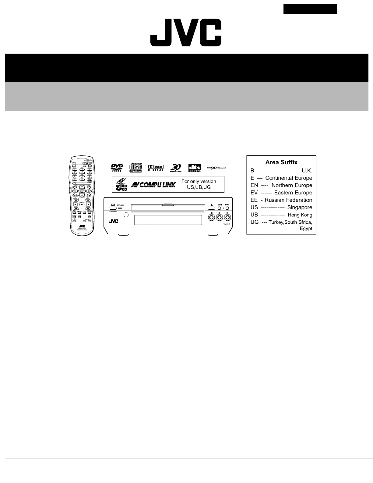
XV-C3SL
SERVICE MANUAL
DVD VIDEO PLAYER
XV-C3SL
COPYRIGHT © 2002 VICTOR COMPANY OF JAPAN, LTD.
No.A0032
2002/08
Page 2

XV-C3SL
TABLE OF CONTENTS
1 Important Safety Precautions . . . . . . . . . . . . . . . . . . . . . . . . . . . . . . . . . . . . . . . . . . . . . . . . . . . . . . . . . . . . . 3
1.1 Safety Precautions . . . . . . . . . . . . . . . . . . . . . . . . . . . . . . . . . . . . . . . . . . . . . . . . . . . . . . . . . . . . . . . . . 3
1.2 Warning. . . . . . . . . . . . . . . . . . . . . . . . . . . . . . . . . . . . . . . . . . . . . . . . . . . . . . . . . . . . . . . . . . . . . . . . . . 3
1.3 Caution . . . . . . . . . . . . . . . . . . . . . . . . . . . . . . . . . . . . . . . . . . . . . . . . . . . . . . . . . . . . . . . . . . . . . . . . . . 3
1.4 Critical parts for safety. . . . . . . . . . . . . . . . . . . . . . . . . . . . . . . . . . . . . . . . . . . . . . . . . . . . . . . . . . . . . . . 3
1.5 Preventing static electricity . . . . . . . . . . . . . . . . . . . . . . . . . . . . . . . . . . . . . . . . . . . . . . . . . . . . . . . . . . . 4
1.6 Handling the traverse unit (optical pickup) . . . . . . . . . . . . . . . . . . . . . . . . . . . . . . . . . . . . . . . . . . . . . . . 4
1.7 Important for laser products . . . . . . . . . . . . . . . . . . . . . . . . . . . . . . . . . . . . . . . . . . . . . . . . . . . . . . . . . . 5
1.8 Precautions for Service. . . . . . . . . . . . . . . . . . . . . . . . . . . . . . . . . . . . . . . . . . . . . . . . . . . . . . . . . . . . . . 6
2 Disassembly method . . . . . . . . . . . . . . . . . . . . . . . . . . . . . . . . . . . . . . . . . . . . . . . . . . . . . . . . . . . . . . . . . . . . 7
2.1 Main body . . . . . . . . . . . . . . . . . . . . . . . . . . . . . . . . . . . . . . . . . . . . . . . . . . . . . . . . . . . . . . . . . . . . . . . . 7
3 MECHANISM . . . . . . . . . . . . . . . . . . . . . . . . . . . . . . . . . . . . . . . . . . . . . . . . . . . . . . . . . . . . . . . . . . . . . . . . . . 10
3.1 Loading assembly section. . . . . . . . . . . . . . . . . . . . . . . . . . . . . . . . . . . . . . . . . . . . . . . . . . . . . . . . . . . 10
3.2 Traverse mechanism assembly section . . . . . . . . . . . . . . . . . . . . . . . . . . . . . . . . . . . . . . . . . . . . . . . . 14
4 Adjustment method . . . . . . . . . . . . . . . . . . . . . . . . . . . . . . . . . . . . . . . . . . . . . . . . . . . . . . . . . . . . . . . . . . . . 17
4.1 Initialization method. . . . . . . . . . . . . . . . . . . . . . . . . . . . . . . . . . . . . . . . . . . . . . . . . . . . . . . . . . . . . . . . 17
4.2 Display of "Laser current value" and "Jitter value" . . . . . . . . . . . . . . . . . . . . . . . . . . . . . . . . . . . . . . . . 17
4.3 Flap adjustment of the pick-up guide shaft . . . . . . . . . . . . . . . . . . . . . . . . . . . . . . . . . . . . . . . . . . . . . . 19
4.4 Attention when pick-up is exchanged . . . . . . . . . . . . . . . . . . . . . . . . . . . . . . . . . . . . . . . . . . . . . . . . . . 21
4.5 Confirm method of operation . . . . . . . . . . . . . . . . . . . . . . . . . . . . . . . . . . . . . . . . . . . . . . . . . . . . . . . . . 22
4.6 Troubleshooting. . . . . . . . . . . . . . . . . . . . . . . . . . . . . . . . . . . . . . . . . . . . . . . . . . . . . . . . . . . . . . . . . . . 23
4.7 Check points for each error. . . . . . . . . . . . . . . . . . . . . . . . . . . . . . . . . . . . . . . . . . . . . . . . . . . . . . . . . . 24
5 Description of major ICs . . . . . . . . . . . . . . . . . . . . . . . . . . . . . . . . . . . . . . . . . . . . . . . . . . . . . . . . . . . . . . . . 27
5.1 74VHC00MTC-X (IC455,IC503) : 2-input nand gate. . . . . . . . . . . . . . . . . . . . . . . . . . . . . . . . . . . . . . . 27
5.2 74VHC74MTC-X (IC454) : ZIVA Wait. . . . . . . . . . . . . . . . . . . . . . . . . . . . . . . . . . . . . . . . . . . . . . . . . . 27
5.3 AN8703FH-V (IC101) : Frontend processor . . . . . . . . . . . . . . . . . . . . . . . . . . . . . . . . . . . . . . . . . . . . . 28
5.4 BA5983FM-X (IC201) : 4CH Driver. . . . . . . . . . . . . . . . . . . . . . . . . . . . . . . . . . . . . . . . . . . . . . . . . . . . 29
5.5 CY24203SC-X (IC571) : MPEG / Audio clock generator with VCXO . . . . . . . . . . . . . . . . . . . . . . . . . . 29
5.6 BA6664FM-X (IC251) : 3Phase Motor Driver . . . . . . . . . . . . . . . . . . . . . . . . . . . . . . . . . . . . . . . . . . . . 30
5.7 74VHCT08ASJ-X (IC704) : 2-input AND gate. . . . . . . . . . . . . . . . . . . . . . . . . . . . . . . . . . . . . . . . . . . . 31
5.8 K3N5V1000FJ004 (IC402) :P2 ROM of 1,048,576word x 16 bit / 2,097,152 word x 8 bit. . . . . . . . . . . 32
5.9 K4S641632F-TC75 (IC504) :CMOS SDRAM . . . . . . . . . . . . . . . . . . . . . . . . . . . . . . . . . . . . . . . . . . . . 33
5.10 MN101C35DLD (IC701) : System controller . . . . . . . . . . . . . . . . . . . . . . . . . . . . . . . . . . . . . . . . . . . . 34
5.11 MN102L62GLH1 (IC401) : Unit CPU . . . . . . . . . . . . . . . . . . . . . . . . . . . . . . . . . . . . . . . . . . . . . . . . . . 35
5.12 MN103S28EGA (IC301) : Super optical disc controller . . . . . . . . . . . . . . . . . . . . . . . . . . . . . . . . . . . . 36
5.13 MM1565AF-X (IC951) : 500mA Regulator . . . . . . . . . . . . . . . . . . . . . . . . . . . . . . . . . . . . . . . . . . . . . . 39
5.14 MN35505-X (IC703) : DAC. . . . . . . . . . . . . . . . . . . . . . . . . . . . . . . . . . . . . . . . . . . . . . . . . . . . . . . . . . 40
5.15 S-93C66AFJ-X (IC451) : EEPROM . . . . . . . . . . . . . . . . . . . . . . . . . . . . . . . . . . . . . . . . . . . . . . . . . . . 41
5.16 STR-G6551-F8 (IC901) : Switch regulator. . . . . . . . . . . . . . . . . . . . . . . . . . . . . . . . . . . . . . . . . . . . . . 41
5.17 MM1566BF-X(IC601):Video signal controller. . . . . . . . . . . . . . . . . . . . . . . . . . . . . . . . . . . . . . . . . . . . 42
5.18 SI-3033LSA-X(IC952):DC Regulator . . . . . . . . . . . . . . . . . . . . . . . . . . . . . . . . . . . . . . . . . . . . . . . . . . 43
5.19 ZIVA-4.1-PB0 (IC501) : Back end - Digital decoder. . . . . . . . . . . . . . . . . . . . . . . . . . . . . . . . . . . . . . . 44
2
Page 3
SECTION 1
Important Safety Precautions
1.1 Safety Precautions
(1) This design of this product contains special hardware and
many circuits and components specially for safety purposes.
For continued protection, no changes should be made to the
original design unless authorized in writing by the
manufacturer. Replacement parts must be identical to
those used in the original circuits. Services should be
performed by qualified personnel only.
(2) Alterations of the design or circuitry o f the product shou ld
not be made. Any design alterations of the product should
not be made. Any design alterations or additions will vo id
the manufacturers warranty and will further relieve the
manufacture of responsibility for personal injury or property
damage resulting therefrom.
(3) Many electrical and mechanical parts in the products have
special safety-related characteristics. These characteristics are often not evident from visual inspection nor can the
protection afforded by them necessarily be obtained by
using replacement components rated for higher voltage,
wattage, etc. Replacement parts which have these specia l
safety characteristics are identified in the Parts List of Service
Manual. Electrical components having such features ar e
identified by shading on the schematics and by ( )
on the Parts List in the Service Manual. The use of a substitute replacement which does not have the same safety
characteristics as the recommended replacement parts
shown in the Parts List of Service Manual may create
shock, fire, or other hazards.
(4) The leads in the products are routed and dressed with ties,
clamps, tubings, barriers and the like to be separated from
live parts, high temperature parts, moving parts and/or
sharp edges for the prevention of electric shock and fire
hazard. When service is required, the original lead routing
and dress should be observed, and it should be confirmed
that they have been returned to normal, after reassembling.
(5) Leakage shock hazard testing)
After reassembling the product, always perform an isolation
check on the exposed metal parts of the product (antenna
terminals, knobs, metal cabinet, screw heads, headphone
jack, control shafts, etc.) to be sure the product is safe to
operate without danger of electrical shock.
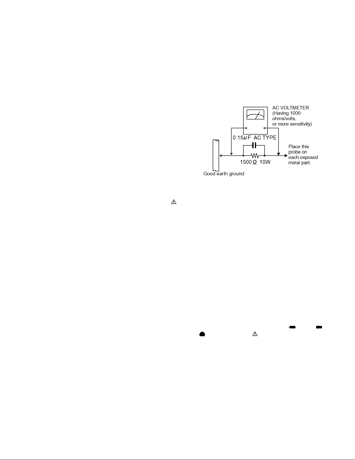
Do not use a line isolation transformer during this check.
• Plug the AC line cord directly into the AC outlet. Using a
"Leakage Current Tester", measure the leakage current
from each exposed metal parts of the cabinet, particularly any exposed metal part having a return path to the
chassis, to a known good earth ground. Any leakage
current must not exceed 0.5mA AC (r.m.s.).
• Alternate check method
Plug the AC line cord direct ly into the AC outle t. Use a n AC
voltmeter having, 1,000 ohms per volt or more sensitivity in
the following manner. Connect a 1,500 ohm 10W resistor
paralleled by a 0.15 µF AC-type capacitor between an
exposed metal part and a known good earth ground.
Measure the AC voltage across the resistor with the AC
XV-C3SL
voltmeter.
Move the resistor connection to each exposed metal part,
particularly any exposed metal part having a return path to
the chassis, and measure the AC voltage across the
resistor. Now, reverse the plug in the AC outlet and repeat
each measurement. Voltage measured any must not
exceed 0.75 V AC (r.m.s.). This corresponds to 0.5 mA AC
(r.m.s.).
1.2 Warning
(1) This equipment has been design ed and manufactured to
meet international safety standards.
(2) It is the legal responsibility of the rep airer to ensure that
these safety standards are maintained.
(3) Repairs must be made in accordance with the relevant
safety standards.
(4) It is essential that safety critical components are replaced
by approved parts.
(5) If mains voltage selector is provided, check setting for lo-
cal voltage.
1.3 Caution
Burrs formed during molding may be left over on some
parts of the chassis.
Therefore, pay attention to such burrs in the case of preforming repair of this system.
1.4 Critical parts for safety
In regard with component parts appearing on the silk-screen
printed side (parts side) of the PWB diagrams, the parts that are
printed over with black such as the resistor ( ), diode ( ) and
ICP ( ) or identified by the " " ma rk nearby are critical for safety.
When replacing them, be sure to use the parts of the same type
and rating as specified by the manufacturer. (Except the JC version)
3
Page 4
XV-C3SL
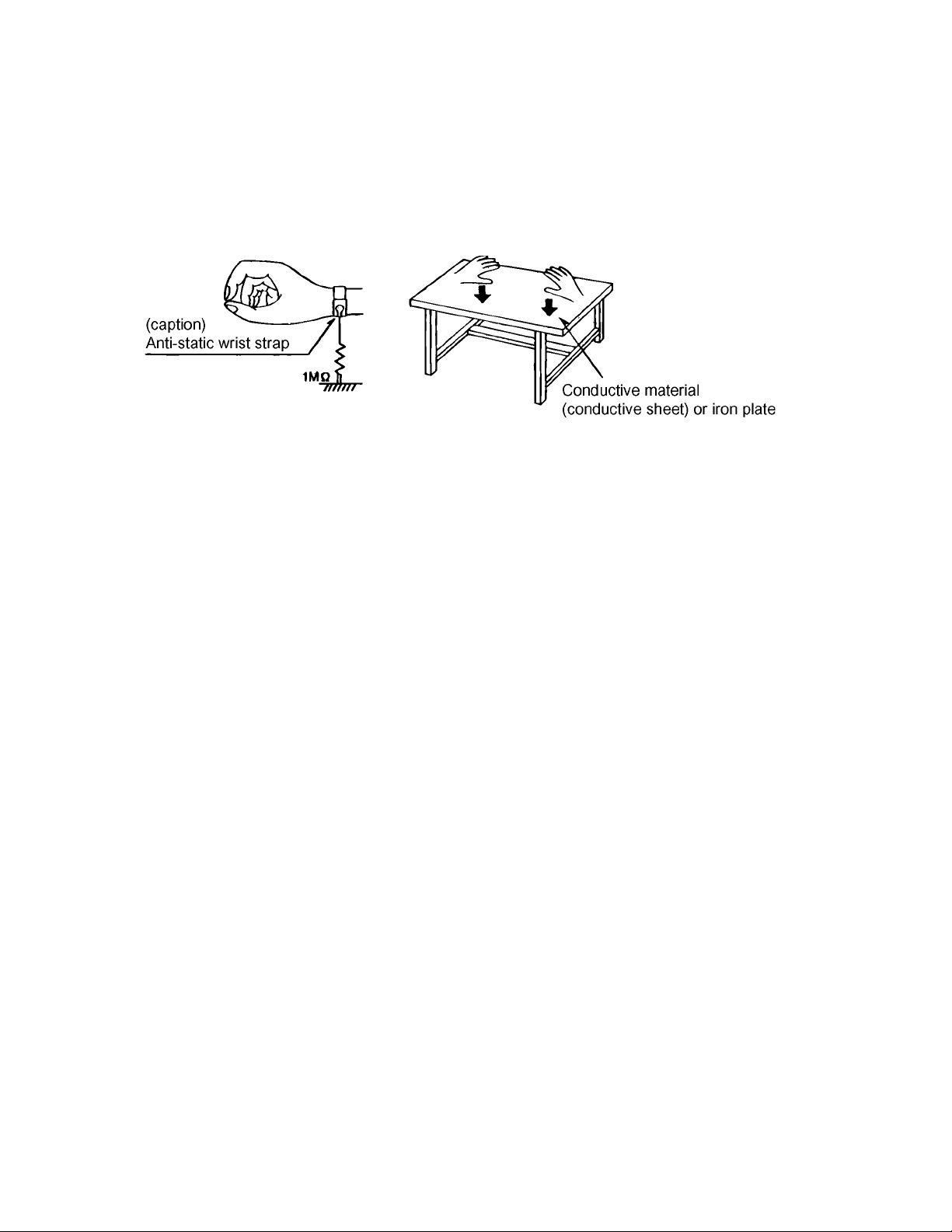
1.5 Preventing static electricity
Electrostatic discharge (ESD), which occurs when static electricity stored in the body, fabric, etc. is discharged,
can destroy the laser diode in the traverse unit (optical pickup). Take care to prevent this when performing repairs.
1.5.1 Grounding to prevent damage by static electricity
Static electricity in the work area can destroy the optical pickup (laser dio de) in devices such as DVD players.
Be careful to use proper grounding in the area where repairs are being performed.
(1) Ground the workbench
Ground the workbench by laying conductive material (such as a conductive sheet) or an iron pl ate over it before placing the
traverse unit (optical pickup) on it.
(2) Ground yourself
Use an anti-static wrist strap to release any static electricity built up in your body.
(3) Handling the optical pickup
• In order to maintain quality during transport and before installation, both sides of the laser diode on the replacement optical
pickup are shorted. After replacement, return the shorted parts to their original condition.
(Refer to the text.)
• Do not use a tester to check the condition of the laser diode in the optical pickup. The tester's i nternal power source can
easily destroy the laser diode.
1.6 Handling the traverse unit (optical pickup)
(1) Do not subject the traverse unit (optical pickup) to strong shocks, as it is a sensitive, complex unit.
(2) Cut off the shorted part of the flexible cable using nippers, etc. after replacing the optical pickup. For specific details, refer to the
replacement procedure in the text. Remove the anti-static pin when replacing the traverse unit. Be careful not to take too
long a time when attaching it to the connector.
(3) Handle the flexible cable carefully as it may break when subjected to strong force.
(4)I t is not possible to adjust the semi-fixed resistor that adjusts the laser power. Do not turn it.
4
Page 5
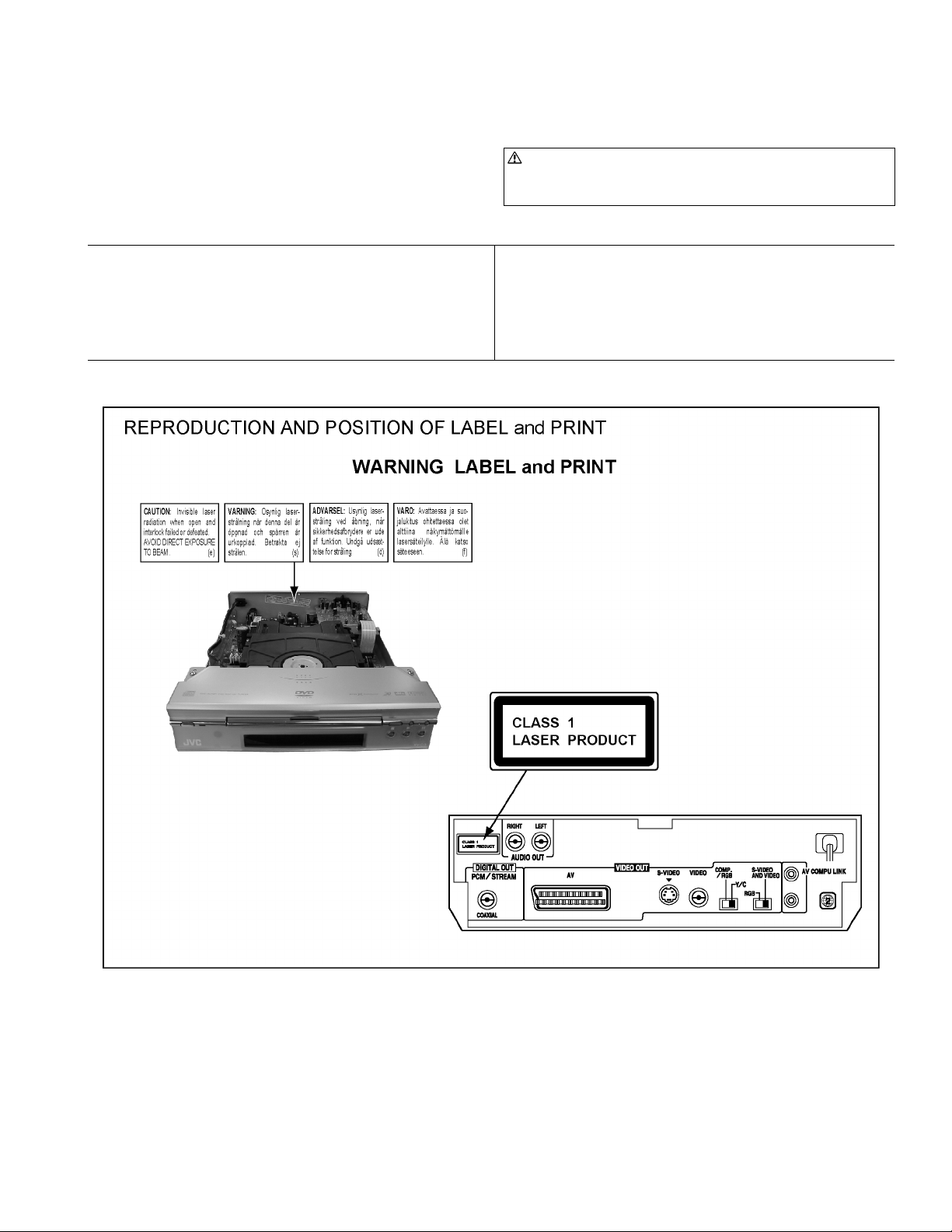
1.7 Important for laser products
(1) CLASS 1 LASER PRODUCT
(2) DANGER : Invisible lase r radiation when open and inter
lock failed or defeated. Avoid direct exposure to beam.
(3) CAUTION : There are no serviceable parts inside the
Laser Unit. Do not disassemble the Laser Unit. Replace
the complete Laser Unit if it malfunctions.
(4) CAUTION : The compact disc player uses in visible laser
radiation and is equipped with safety switches which
prevent emission of radiation when the drawer is open and
the safety interlocks have failed or are de feated.
It is dangerous to defeat the safety switches.
VARNING
Osynlig laserstrålning är denna del är öppnasd och spårre n är
urkopplad. Betrakta ej strålen.
VARO
Avattaessa ja suojalulitus ohitettaessa olet alttiina näkymättömälle lasersateilylle. Älä katso säteeseen.
REPRODUCTION AND POSITION OF LABEL and PRINT
WARNING LABEL
XV-C3SL
(5) CAUTION : If safety switches malfunction, the laser is able
to function.
(6) CAUTION : Use of controls, adjustments or perfo rmance
of procedures other than those specified herein may result
in hazardous radiation exposure.
CAUTION
Please use enough caution not to see the beam dir ectly
or touch it in case of anadjustment or operation check.
ADVARSEL
Usynlig laserstrling ved åbning, når sikkerhedsafbrydere er
ude af funktion. Undgå udsasttelse for stråling.
ADVARSEL
Usynlig laserstråling ved åpning, når sikkerhetsbryteren er
avslott. unngå utsettelse for stråling.
5
Page 6
XV-C3SL
1.8 Precautions for Service
1.8.1 Handling of Traverse Unit and Laser Pickup
(1) Do not touch any peripheral element of the pickup or the actuator.
(2) The traverse unit and the pickup are precision devices and therefore must not be subjected to strong shock.
(3) Do not use a tester to examine the laser diode. (The diode can easily be destroyed by the internal power supply of the tester.)
(4) To replace the traverse unit, pull out the metal short pin for protection from charging.
(5) When replacing the pickup, after mounting a new picku p, remove the solder on th e short land which is provide d at the center
of the flexible wire to open the circuit.
(6) Half-fixed resistors for laser power adjustment are adjusted in pairs at shipment to match the characteristics of the optical block.
Do not change the setting of these half-fixed resistors for laser power adjustment.
1.8.2 Destruction of Traverse Unit and Laser Pickup by Static Electricity
Laser diodes are easily destroyed by static electricity charged on clothing
or the human body. Before repairing peripheral elements of the traverse unit or pickup, be sure to take the following electrostatic
protection:
(1) Wear an antistatic wrist wrap.
(2) With a condu ctive sheet or a steel plate o n the workbench on wh ich the traverse unit or the pick up is to be repaired, groun d
the sheet or the plate.
(3) After removing the flexibl e wire from the connector (CN101), short-circuit the flexible wire by the metal clip.
(4) Short-circuit the laser diode by soldering the land which is provided at the center of the flexible wire for the pickup.
After completing the repair, remove the solder to open the circuit.
Please refer to "Fig.6" of "Disassembly method" for details.
6
Page 7
SECTION 2
Disassembly method
2.1 Main body
There is a part different from the photograph a ccording to the
model and the destination though explains this disassembly
method by using XV-C3SL for Europe.
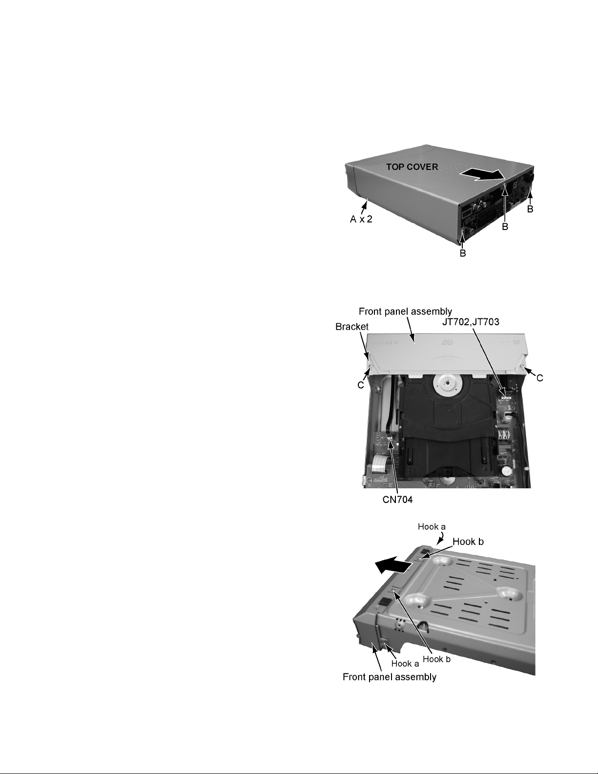
2.1.1 Removing the top cover
(see Fig.1)
(1) Remove the two screws A attaching the top cover on both
sides of the body.
(2) Remove the three screws B attaching the top cover on the
back of the body.
(3) The slide is done backward and a top cover is removed.
2.1.2 Removing the front panel assembly and bracket
(see Fig.2,3)
• Prior to performing the following procedure, remove the top cover.
(1) Disconnect the flat wire from connector CN704,JT702,
JT703 on the main board.
(2) Fou r plac es in hook a and b are removed, the front panel as-
sembly is slide to forward and it is removed.
(3) Remove the two screws C attaching the bracket.
XV-C3SL
Fig.1
Fig.2
Fig.3
7
Page 8
XV-C3SL
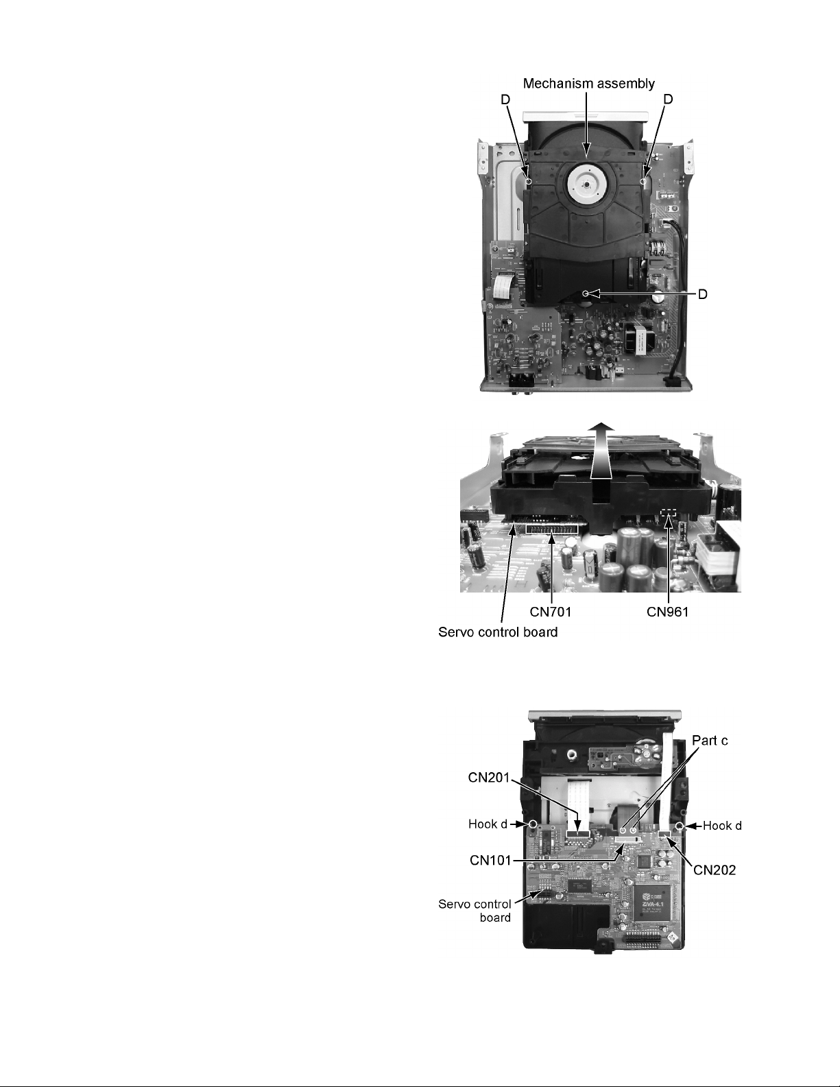
2.1.3 Removing the mechanism assembly
(see Fig.4,5)
• Prior to performing the following procedure, remove the top
cover, front panel assembly and bracket.
(1) Remove the three screws D attaching the mechanism as-
sembly.
(2) The servo control board is removed from the connector
CN961 and CN701 connected with the main board respectively.
Fig.4
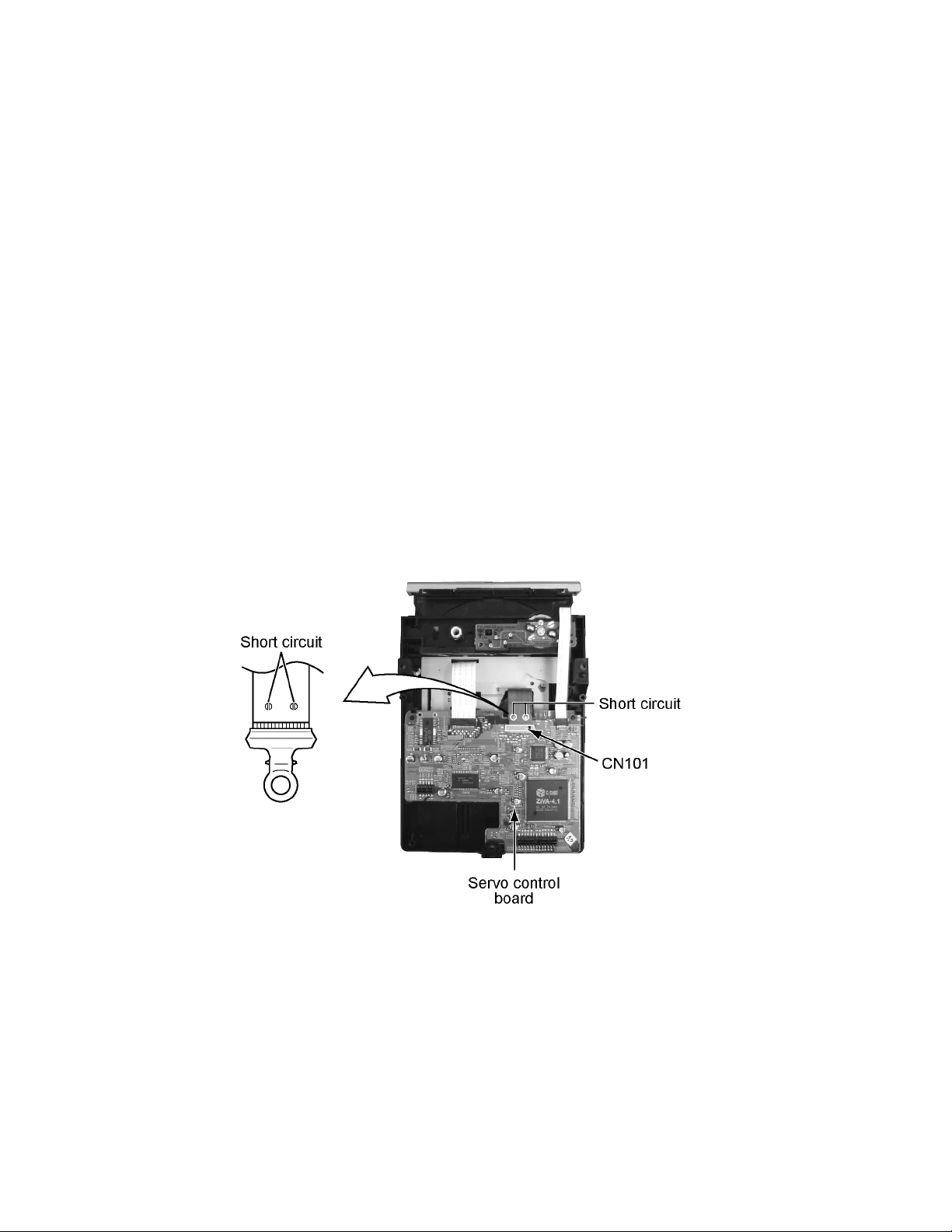
2.1.4 Removing the servo control board
(see Fig.6)
• Prior to performing the following procedure, remove the top
cover, front panel assembly, bracket and mechanism assembly.
(1) Disconnect the card wire from connector CN201 and
CN202 on the servo control board respectively.
(2) Disconnect the flexible wire from connector CN101 on the
servo control board from pick-up
ATTENTION:
At this time, please extract the wire after short-circuited of two places on the wire in part c with solder.
Please remove the solder two places of part c after
connecting the wire with CN101 when reassembling.
(3) Two places in hook d are removed, the servo control
board is lifted, and it is removed.
Fig.5
Fig.6
8
Page 9
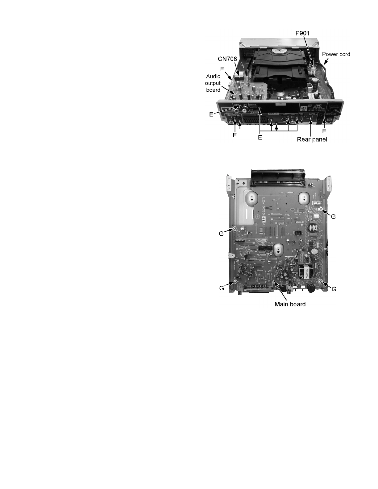
2.1.5 Removing the rear panel and audio output board
(see Fig.7)
• Prior to performing the following procedure, remove the top
cover.
(1) Remove the nine screws E attaching the rear pane l.
(2) Disconnect the card wire fro m connector CN706 on the
audio output board.
(3) Remove the one screw F attaching the audio output board.
(4) Disconnect the power cord from socket P901 on the main
board.
2.1.6 Removing the main board
(see Fig.8)
• Prior to performing the following procedure, remove the top
cover, front panel assembly, bracket, mechanism assembly,
rear panel and audio output board.
(1) Remove the four screws G attaching the main board.
XV-C3SL
Fig.7
Fig.8
9
Page 10
XV-C3SL
SECTION 3
MECHANISM
3.1 Loading assembly section
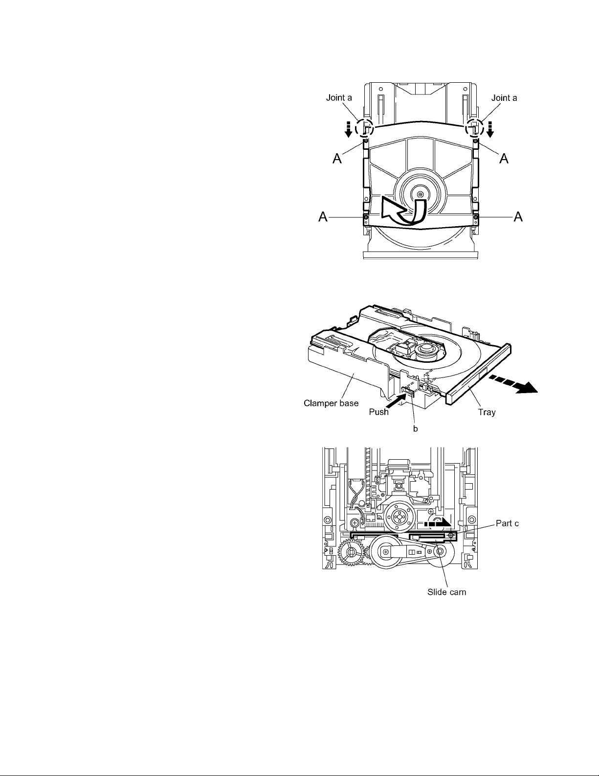
3.1.1 Removing the clamper assembly
(See Fig.1)
(1) Remove the four screws A attaching the clamper assembly.
(2) Move the clamper in the direction of the arrow to release
the two joints a on both sides.
ATTENTION:
When reattaching, fit the clamper to the two joints a.
3.1.2 Removing the tray
(See Fig2. and 3)
• Prior to performing the following procedure, remove the
clamper assembly.
(1) Push b of the slide cam into the slot on the left side of the
loading base until it stops.
(2) Draw out the tray toward the front.
Fig.1
ATTENTION:
Before reattaching the tray, slide the part c of the slide
cam to the right as shown in Fig.2.
Fig.2
Fig.3
10
Page 11
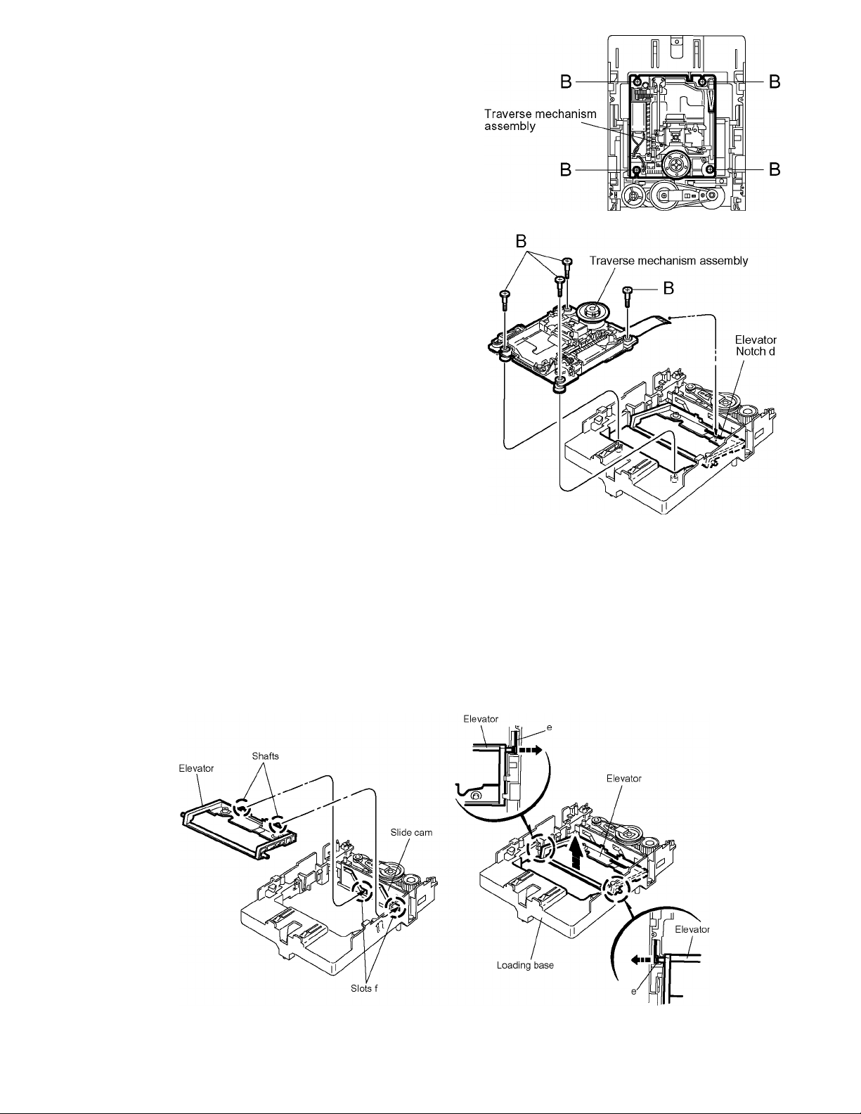
3.1.3 Removing the traverse mechanism assembly
(See Fig.4 and 5)
• Prior to performing the following procedure, remove the
clamper assembly and the tray.
(1) Remove the four screws B attaching the traverse mechanism
assembly.
ATTENTION:
Before reattaching the traverse mechanism assembly,
pass the card wire extending from the spindle motor
board through the notch d of the elevator.
XV-C3SL
Fig.4
3.1.4 Removing the elevator
(See Fig.6)
• Prior to performing the following procedure, remove the
clamper assembly, the tray and the traverse mechanism assembly.
(1) Extend each bar e inside of the loading base
outward and detach the elevator shaft.
ATTENTION:
When reattaching, first fit the two shafts on the
front of the elevator to the slots f of the slide cam.
Fig.5
Fig.6
11
Page 12
XV-C3SL
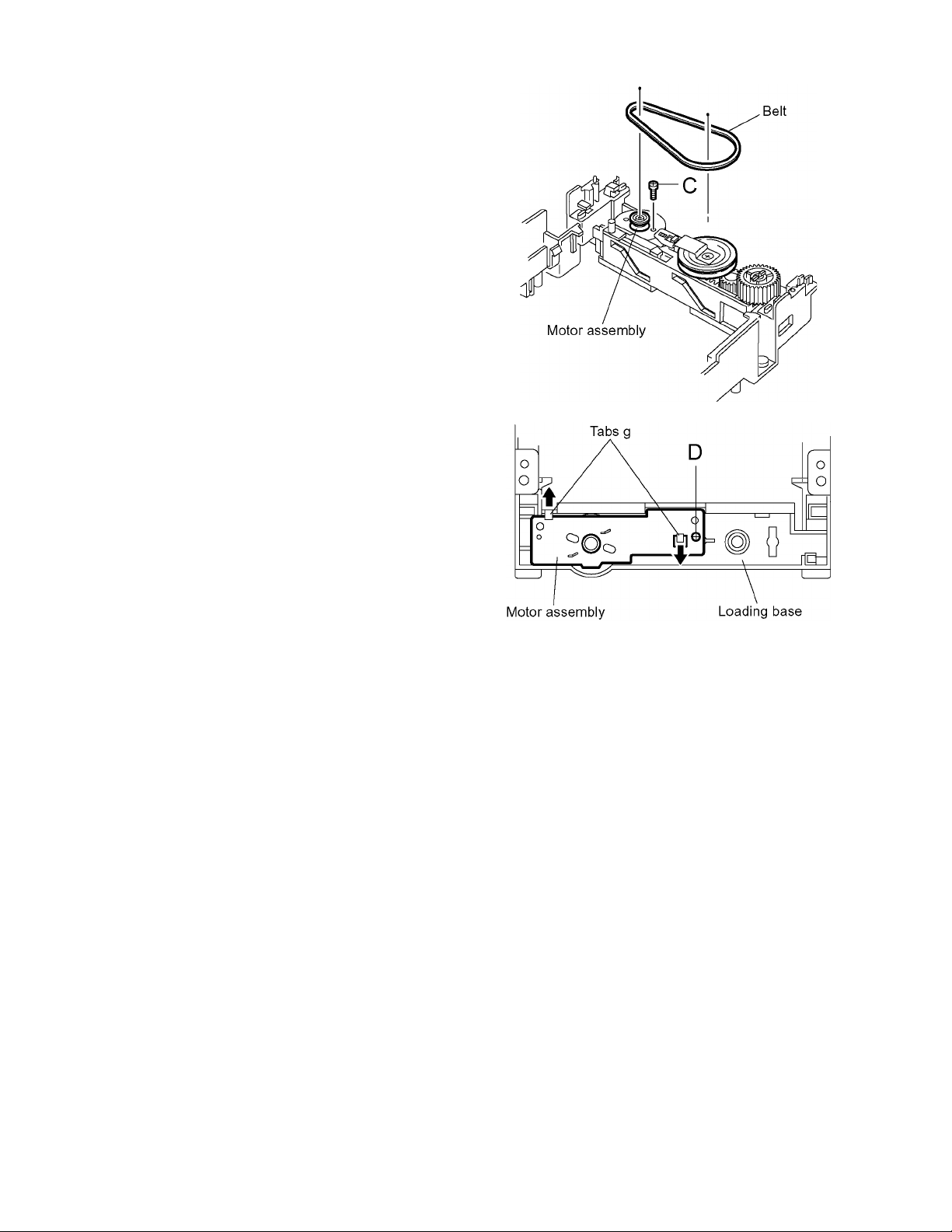
3.1.5 Removing the motor assembly
(See Fig.7 and 8)
• Prior to performing the following procedure, remove the
clamper assembly, the tray.the traverse mechanism assembly
and the elevator.
(1) Remove the belt from the pulley.
(2) Remove the screw C attaching the motor assembly.
(3) Turn over the body and remove the screw D attaching the
motor assembly.
(4) Release the two tabs g retaining the motor board.
Fig.7
Fig.8
12
Page 13
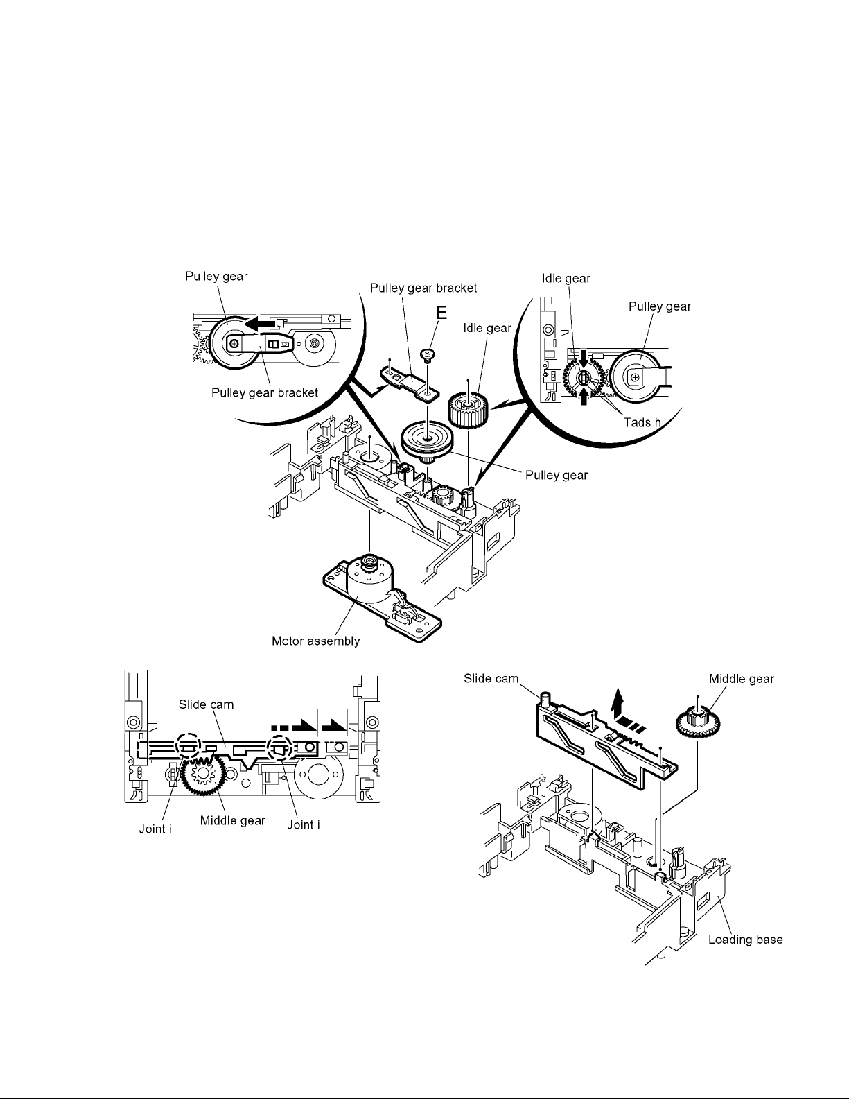
3.1.6 Removing the Idle gear/pully gear/
middle gear/slitecam
(See Fig.9 to 11)
• Prior to performing the followong procedure,remove
the clamper assembly,the tray,the traverse m ec ha n is m
assembly,the elevator and the motor assembly.
(1) Press the two tabs h inward and pull out idle gear.
(2) Remove the screw E attaching the pulley gear bracket.
Slide the pulley gear bracket in the direction o f the
arrow and pull out the pulley gear.
(3) Slide the side cam in the direction of the arrow to
release the two joints i and remove upward.
(4) Remove the middle gear.
XV-C3SL
Fig.10
Fig.9
Fig.11
13
Page 14
XV-C3SL
3.2 Traverse mechanism assembly section
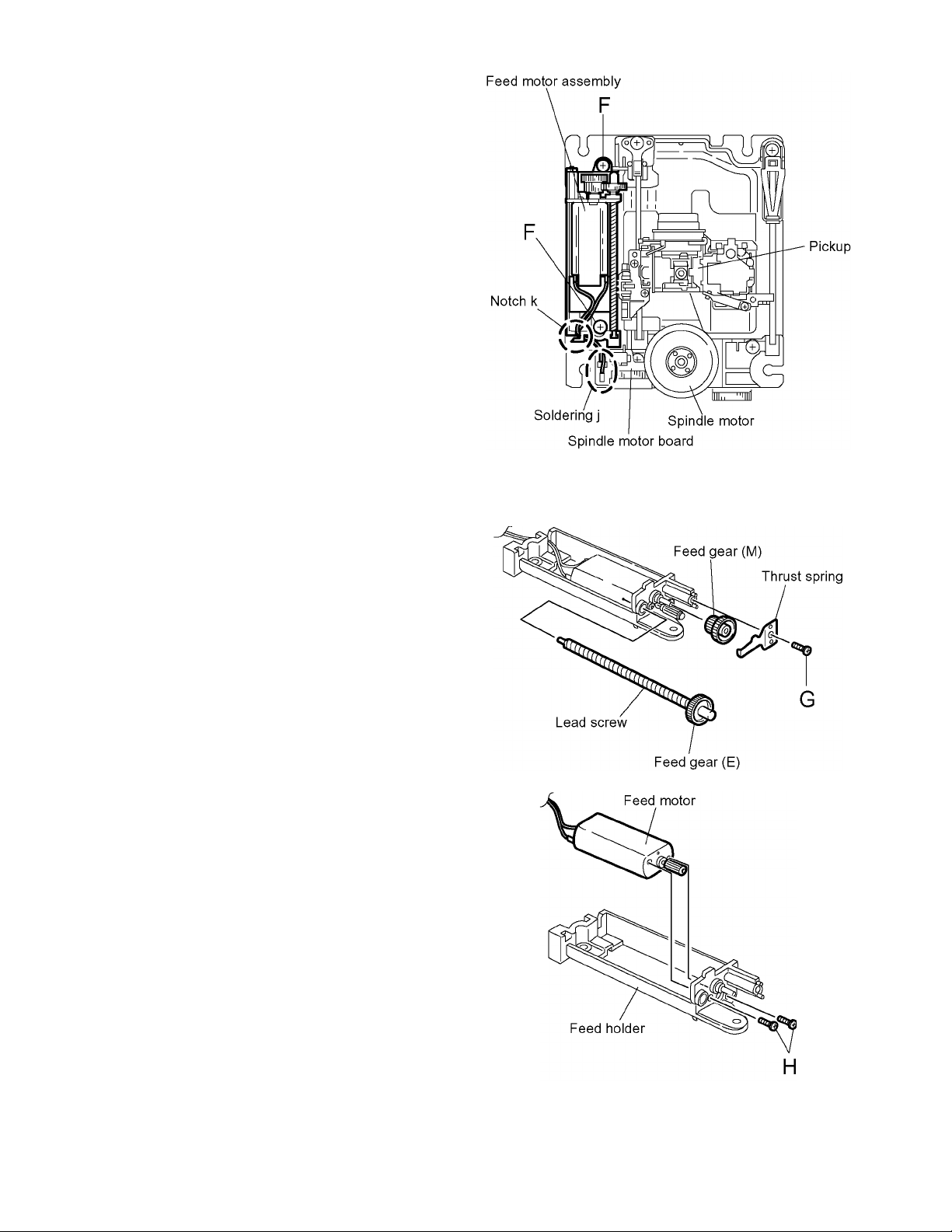
3.2.1 Removing the feed motor assembly
(See Fig.12)
(1) Unsolder the two soldering j on the spindle motor board.
(2) Remove the four screws F attaching the feed motor as -
sembly.
3.2.2 Removing the feed motor
(See Fig.12 to 14)
Fig.12
• Prior to performing the following procedure, remove the feed
motor assembly.
(1) Remove the screw G attaching the thrust spring.
ATTENTION:
When reattaching the thrust spring, make sur e that
the thrust spring presses the feed gear (M) and the
feed gear (E) reasonably.
(2) Remove the feed gear (M).
(3) Pull out the feed gear (E) and the lead screw.
(4) Remove the two screws H attaching the feed motor.
ATTENTION:
When reattaching, pass the two cables extending
from the feed motor through the notch k of the feed
holder as shown in Fig12.
Fig.13
14
Fig.14
Page 15

3.2.3 Removing the pickup
(See Fig.16 and 18)
(1) Remove the screw I attaching the T spring (S) and the
shaft holder. Remove also the plate.
ATTENTION:
When rea t ta c hi n g, make sure that the T s pring (S)
presses the shaft.
(2) Pull out the part l of the shaft upward. Move the part m in
the direction of the arrow and detach from the spindle
base.
(3) Disengage the joint n of the pickup and the shaft in the di-
rection of the arrow.
(4) Pull out the shaft from the pickup.
(5) Remove the two screws J attaching the actuator.
(6) Disengage the joint of the actu ator and the lead spring.
Pull out the lead spring.
XV-C3SL
Fig.16
Fig.15
The spring must be under the shaft when you
install pick-up.
3.2.4 Removing the shaft holder / shaft
(See Fig.18)
(1) Remove the screw K attaching the shaft holder.
(2) Remove the shaft.
Fig.17
Fig.18
15
Page 16

XV-C3SL
3.2.5 Removing the spindle motor assembly
(See Fig.19 to 21)
(1) Remove the three screws L attaching the spindle motor on
the bottom of the mechanism base.
ATTENTION:
When reattaching, pass the card wire extending from
the spindle motor board through the notch of the spindle base.
(2) Remove the three screws M attaching the spindle base.
Fig.19
Fig.20
Fig.21
16
Page 17

SECTION 4
Adjustment method
4.1 Initialization method
If microprocessor (IC401,IC402,IC451) or pick-up is replaces, initialize the
DVD player in the following matter
(1) Take out the disc and close the tray.
(2) Unplug the power plug.
(3) Insert power plug into outlet while pressing both "PLAY" butto n and "OPEN/CLOSE" button.
(4) FL Display indicate "TEST * * #" , * * :Version, #" :Region code
(5) Press "3D-PHONIC" button of remote controller. and EEPROM initialize start.
(6) When indicate "DTS" on the FL display, initialize finishes.
(7) The power is turned OFF, and Unplug the power plug.
4.2 Display of "Laser current value" and "Jitter value"
"Laser current value" and "Jitter value" are displayed on the FL display by the undermentioned
method. Please refer to the failure diagnosis.
(1) Take out the disc and close the tray.
(2) Unplug the power plug.
(3) Insert power plug into outlet while pressing both "PLAY" butto n and "OPEN/CLOSE" button.
(4) FL Display indicate "TEST * * #" , * * :Version, #" ::Region code
(5) Press the "OPEN/CLOSE" button to move the tray outward.
Put the test disc (VT-501) on the tray and press "OPEN/CLOSE" button.
The tray should move inward (Note:Don't push to close the tray directly by hand etc.)
(6) Press the "PLAY" button.
(7) After a few seconds, the laser current value and the jitter value is displayed on the FL indicator as follows.
XV-C3SL
Fig.1
4.2.1 For Laser current value
The laser current value becomes 35mA for the above-mentioned.
Becomes a test mode by doing above-mentioned procedure 1) - 4). Afterwards, the laser current value can
be switched by pushing the button to remote controller without turning on the disk.
Remote control "4" button --- Laser of CD *Returns to a usual test mode by the
Remote control "5" button --- Laser of DVD thing to push the "STOP" button of
It can be judged it is simply good if the displayed current value of the laser is smaller than that of the undermentioned value.
Moreover, there must be a deteriorated possibility and the pick-up must exch ange the pick-up more than the undermentioned value.
Laser current value of CD ------ 49 mA or less
Laser current value of DVD ---- 64 mA or less
remote controller.
Fig.2
17
Page 18

XV-C3SL
4.2.2 For Jitter value
The jitter value is displayed on the FL display referring to the previous page.
The jitter value is displayed by the hexadecimal number.
In the following cases, please "Flap adjustment of the pick-up guide shaft" referring to the following page.
Before using the TEST disc VT-501, careful check it if there is neither damage nor dirt on the read surface.
Returns to a usual test mode by the thing to push the "STOP" button ot remote controller.
< In the following cases, please adjustment >
• When you exchange the pick-up
• When you exchange the spindl e motor
• When the reading accuracy of the signal is bad (There is a block noise in the screen etc..)
Fig.3
18
Page 19

4.3 Flap adjustment of the pick-up guide shaft
4.3.1 Tool list for adjustment
• Hex wrench for adjustment
Off-the-shelf (1.3mm)
• Test disc
VT-501 or VT-502
• Stud (four pieces set)
Parts No. : JIGXVS40 (One is not used though there are four. )
Fig.4
• Assistance board and extension cord
XV-C3SL
4.3.2 Connection diagram
Fig.5
Fig.6
19
Page 20

XV-C3SL
4.3.3 Adjustment preparation
(1) The mechanism assembly is made in the state from the main body from which is detached referring to the disassembly method.
(2) Three studs are installed in the mechanism assembly respectively.
(3) The servo control board is removed from th e mechanism asse mb ly, a nd puts into the state se t up as shown in figure. (Each
wire connected by the servo control board this time leaves the connection maintained.)
Between shaft and hook of mechanism assembly of figure Board is put.
(4) The extension cord is inserted in the connector of the assistance board respectively.
The main board is connected with the servo control board as shown in figure.
Fig.7
4.3.4 Adjustment
(1) Puts into the state to display the jitter value on the FL disp lay referring to "Display of the jitter value".
(2) The adjustment screw under the traverse mechanism is turned with hex wrench, and matches so that the jitter value displayed
on the FL display may become "maximum" value.
<POINT>
(1) Turns in the forward or the opposite direction,and
makes to the position where the jitter value i s good the
half rotation of adjustment screw a and b(180 de grees)
respectively.
(2) Afterwards, adjustment screw b a nd c are turned in the
same way, and makes to the best position.
<ATTENTION>
(1) Values to judge whether the jitter is allowable or not is
displayed, instead of actual jitter values.
The displayed values are expressed in hexadecimal
Fig.9
numbers.
(2) As this value is bigger, the jitter is more allowable in this
model.
Fig.8
20
Page 21

4.4 Attention when pick-up is exchanged
(1) Flexible wire, pick-up spring, switch actuator, and lead
spring are removed from an old pick-up(broken the one).
< Guide >
Flexible wire, pick-up spring and switch actuator,
lead spring are removed without each decomposing
while assembled.
(2) The above-mentioned parts are installed in a new pick-up
(non-defective article).
(3) A flexible wire is inserted in the connector which has taken
side with the pick-up, and solder is put up to short land part
"a" two places on a flexible wire.
(4) The electrostatic breakdown protection circuit attached
to the pick-up is cut.
< ATTENTION >
Please cut the electrostatic breakdown protection
circuit attached to the pick-up after solder is put up
to two places on a flexible wire short land part "a" of
the insertion of a flexible wire this time in the connector without fail.
The procedure might be mistaken and if solder has
not surely adhered to two places on a flexible wire
short land part "a", the laser diode in the pick-up be
destroyed again.
XV-C3SL
Fig.3-10
(5) The pick-up is installed in the traverse mechanism.
(6) A flexible wire is connected with connector CN101 on the-
servo control board by installing the traverse mechanism
in the loading mechanism.
(7) Solder in two places on a flexible wire in part "a" is re-
moved.
< ATTENTION >
Please remove solder in two places in part "a" after
connecting a flexible wire with connector CN101 on
the servo control board without fail this time.
When the procedure is mistaken, the laser diode in
the pick-up might be destroyed.
Please remove solder in two places in part "a" surely.
Fig.3-11
Fig.3-12
Fig.3-13
21
Page 22

XV-C3SL
4.5 Confirm method of operation
Please confirm the operation of the undermentioned item after doing the repair and
the upgrade of the firmware.
The EEPROM is initialized.
Refer to the initialization method.
Opening picture check (Power ON)
It should be display "JVC"
Muting working
The noise must not be had to the performance beginning when you push "PLAY" button or at ON/STANDBY.
FL Display
The mark and the logo, etc. displayed by each operation must be displayed correctly.
FL Display should light correctly without any unevenness.
All Function button
All function buttons should worked correctly with moderate click feeling.
Open and close movement of tray
When press OPEN/CLOSE button the tray should move smoothly without any noise.
Remote controller unit working
Check the correctly operation in use of remote controller unit.
Reading of TOC
Be not long in the malfunction.
Search
Both forward-searches and backward-searches should be able to be done.
Do not stop be searching or after the search.
Skip
Both forward-skip and backward-skip should be able to be done.
Do not stop be after the skip.
Playback
Do not find abnormality etc. of tone quality and the picture quality.
Most outside TITLE playback check
Play VT-501 TITLE 59 CHAPTER 1 , check normal playback.
22
Page 23

4.6 Troubleshooting
4.6.1 Servo volume
XV-C3SL
Fig.14
23
Page 24

XV-C3SL
4.7 Check points for each error
4.7.1 Spindle start error
(1) Defective spindle motor
• Are there several ohms resistance between each pin of CN201 "5-6","6-7","5-7"?
(The power supply is turned off and measured.)
• Is the sign wave of about 100mVp-p in the voltage had from each terminal?
[ CN201"9"(H1-),"10"(H1+),"11"(H2-),"12"(H2+),"13"(H3-),"14"(H3+) ]
(2) Defective spindle motor driver (IC251)
• Has motor drive voltage of a sine wave or a rectangular wave gone out to each terminal(SM1~3)
of CN201"5,6,7" and IC251"2,4,7"?
• Is FG pulse output from the terminal of IC251"24"(FG) according to the rotation of the motor?
• Is it "L(about 0.9V)" while terminal of IC251"15"(VH) is rotating the motor?
(3) Has the control signal come from servo IC or the microcomputer?
• Is it "L" while the terminal of IC251"18"(SBRK) is operating?
Is it "H" while the terminal of IC251"23"(/SPMUTE) is operating?
• Is the control signal input to the terminal of IC251"22"(EC)?
(changes from VHALF voltage while the motor is working.)
• Is the VHALF voltage input to the terminal of IC251"21"(ECR)?
(4) Is the FG signal input to the servo IC?
• Is FG pulse input to the terminal of IC301"69"(FG) according to the rotation of the motor?
4.7.2 Disc Detection, Distinction error (no disc, no RFENV)
• Laser is defective.
• Front End Processor is defective (IC101).
• APC circuit is defective. --- Q101,Q102.
• Pattern is defective. --- Lines for CN101 - All patterns which relate to pick-up and patterns between IC101
• IC101 --- For signal from IC101 to IC301, is signal output from IC101 "20" (ASOUT) and
IC101 "41"(RFENV) and IC101 "22" (FEOUT)?
• Servo IC is defective (IC301)
24
Page 25

XV-C3SL
4.7.3 Traverse movement NG
(1) Defective traverse driver
• Has the voltage come between terminal of CN101 "1" and "2" ?
(2) Defective BTL driver (IC201)
• Has the motor drive voltage gone out to IC201"17" or "18"?
(3) Has the control signal come from servo IC or the microcomputer?
• Is it "H" while the terminal of IC201"9"(STBY1) ?
• TRSDRV Is the signal input? (IC301 "67")
(4) TRVSW is the signal input from microcomputer? (IC401 "46")
4.7.4 Focus ON NG
• Is FE output ? --- Pattern, IC101
• Is FODRV signal sent ? (R209) --- Pattern, IC301 "115"
• Is driving voltage sent ?
IC201 "13", "14" --- If NG, pattern, driver, mechanical unit .
• Mechanical unit is defective.
4.7.5 Tracking ON NG
• When the tracking loop cannot be drawn in, TE shape of waves does not settle.
• Mechanical unit is defective.
Because the self adjustment cannot be normally adjusted, the thing which cannot be normally drawn in is thought.
• Periphery of driver (IC201)
Constant or IC it self is defective.
• Servo IC (IC301)
When improperly adjusted due to defective IC.
4.7.6 Spindle CLV NG
• IC101 -- "35"(RF OUT), "30"(ARF-), "31(ARF+).
• Does not the input or the output of driver's spindle signal do the grip?
• Has the tracking been turned on?
• Spindle motor and driver is defective.
• Additionally, "IC101 and IC301" and "Mechanism is defective(jitter)", etc. are thought.
4.7.7 Address read NG
• Besides, the undermentioned cause is thought though specific of the cause is difficult because various actors are thought.
Mechanism is defective. (jitter)
IC301, IC401.
The disc is dirty or the wound has adhered.
4.7.8 Between layers jump NG (double-layer disc only)
Mechanism defective
Defect of driver's IC(IC201)
Defect of servo control IC(IC301)
25
Page 26

XV-C3SL
[When DVD usually reproduces]
4.7.9 Neither picture nor sound is output
(1) It is not possible to search
• Has the tracking been turned on?
• To "(4.7.5) Tracking ON NG" in "Check points for each error" when the tracking is not normal.
• Is the feed operation normal?
To "(4.7.3) traverse movement NG" in "Check points for each error" when it is not normal.
Are not there caught of the feeding mechanism etc?
4.7.10 Picture is distorted or abnormal sound occu rs at intervals of several seconds.
Is the feed operation normal?
Are not there caught of the feeding mechanism etc?
4.7.11 Others
The image is sometimes blocked, and the image stops.
The image is blocked when going to outer though it is
normal in surroundings in the disk and the stopping
sympton increases.
[When CD usually reproduses]
4.7.12 CD During normal playback operation
There is a possibility with bad jitter
value for such a symptom.
26
Page 27

SECTION 5
Description of major ICs
5.1 74VHC00MTC-X (IC455,IC503) : 2-input nand gate
• Pin layout • Truth table
ABY
LLH
LHH
HLH
HHL
L : High impedance
5.2 74VHC74MTC-X (IC454) : ZIVA Wait
• Terminal layout
• Trouth table
XV-C3SL
• Pin function
Pin No. Symbol I/O Description Pin No. Symbol I/O Description
1 CLR1 I Direct clear input 1 8 Q2 O Output
2 D1 I Data input 1 9 Q2 O Output
3 CK1 I Clock pulse input 1 10 PR2 I Direct preset input 2
4 PR1 I Direct preset input 1 11 CK2 I Cl ick pulse in put 2
5 Q1 O Output 12 D2 I Data input 2
6 Q1 O Output 13 CLR2 I Clock clear input 2
7 GND - Connect to ground 14 VCC - Power supply
27
Page 28

XV-C3SL
5.3 AN8703FH-V (IC101) : Frontend processor
• Pin layout
• Pin function
Pin No.
10 IDGT I Data slice part address part gate signal in-
11 STANDBY I Standby mode control terminal 46 TESTSG I TEST signal input terminal
12 SEN I SEN(Serial data input terminal) 47 RFINP I RF signal positive input terminal
13 SCK I SCK(Serial data input terminal) 48 RFINN I RF signal negative input terminal
14 STDI I STDI(Serial data input terminal) 49 VIN5 I Internal four-partition (CD) RF input 1
15 RSCL I Standard electric current terminal 50 VIN6 I Internal four-partition (CD) RF input 2
16 JLINE I Electric current setting terminal of JLine 51 VIN7 - Internal four-partition (CD) RF input 3
17 TEN I Reversing input terminal of tracking error
18 TEOUT O Tracking error signal output terminal 53 VIN9 I External two-partition (DVD) RF input 2
19 AGCBAL I Offset adjusting terminal 1 54 VIN10 I External two-partition (DVD) RF input 1
20 ASOUT O Full adder signal output terminal 55 VCC1 - Power supply terminal 5V
21 FEN I Focus error output amplifier reversing input
22 FEOUT O Focus error signal output terminal 57 VIN1 I Internal four-partition (DVD) RF input 1
23 AGCOFST I Offset adjusting terminal 2
24 MON - Non connect 58 VIN2 I Internal four-partition (DVD) RF input 2
25 AGCLVL O Output amplitude adjustment for DRC
26 GND2 - Connect to GND 59 VIN3 I Internal four-partition (DVD) RF input 3
27 VREF2 O VREF2 voltage output terminal
28 VCC2 - Power supply terminal 5V 60 VIN4 I Internal four-partition (DVD) RF input 4
29 VHALF O VHALF voltage output terminal
30 DFLTON O Reversing output terminal of filter AMP. 61 GND1 - Connect to GND
31 DFLTOP O Filter AMP. output terminal 62 VIN11 I 3 beam sub input terminal 2 (CD)
32 DCFLT I Capacity connection terminal for filter out-
33 GND3 - Connect to GND 64 HDTYPE O HD Type selection
Symbol I/O Description
1 LPC1 I Laser input terminal (DVD) 34 RFDIFO - Non connect
2 LPC01 O Laser drive signal output terminal (DVD) 35 RFOUT - Connect to TP103
3 LPC2 I Laser input terminal (CD) 36 VCC3 - Power supply terminal 3.3V
4 LPC02 O Laser drive signal output terminal (CD) 37 RFC O Filter for RF delay correction AMP.
5
VFOSHORT
6 TBAL I Tracking balance control terminal 39 OFTR O OFTR output terminal
7 FBAL I Focus balance control t erminal 40 BDO O BDO output terminal
8 POFLT O Track detection threshold level terminal 41 RFENV O RF envelope output terminal
9 D TRD I Data slice part data read signal input termi-
I VFOSHORT control terminal 38 DCRF O All addition amplifier capacitor terminal
nal(For RAM)
put terminal( For RAM)
output AMP.
terminal
put
Pin No.
42 BOTTOM O Bottom envelope detection filter terminal
43 PEAK O Peak envelope detection filter terminal
44 AGCG O AGC amplifier gain control terminal
45 AGCO O AGC amplifier level control terminal
52 VIN8 - Internal four-partition (CD) RF input 4
56 VREF1 O VREF1 voltage output terminal
63 VIN12 I 3 beam sub input terminal 1 (CD)
Symbol I/O Description
28
Page 29

5.4 BA5983FM-X (IC201) : 4CH Driver
• Block diagram
• Pin function
Pin No.
Symbol I/O Description
1 BIAS IN I Input for Bias-amplifier 16 VO4(-) O Inverted output of CH4
2 OPIN1(+) I Non inverting input for CH1 OP-AMP 17 VO3(+) O Non inverted output of CH3
3 OPIN1(-) I Inverting input for CH1 OP-AMP 18 VO3(-) O Inverted output of CH3
4 OPOUT1 O Output for CH1 OP-AMP 19 PowVcc2 - Vcc for CH3/4 power block
5 OPIN2(+) I Non inverting input for CH2 OP-AMP 20 STBY2 I Input for Ch4 stand by control
6 OPIN2(-) I Inverting input for CH2 OP-AMP 21 GND - Substrate ground
7 OPOUT2 O Output for CH2 OP-AMP 22 OPOUT3 O Output for CH3 OP-AMP
8 GND - Substrate ground 23 OPIN3(-) I Inverting input for CH3 OP-AMP
9 STBY1 I Input for CH1/2/3 stand by control 24 OPIN3(+) I Non inverting input for CH3 OP-AMP
10 PowVcc1 - Vcc for CH1/2 power block 25 OPOUT4 O Output for CH4 OP-AMP
11 VO2(-) O Inverted output of CH2 26 OPIN4(-) I Inverting input for CH4 OP-AMP
12 VO2(+) O Non inverted output of CH2 27 OPIN4(+) I Non inverting input for CH4 OP-AMP
13 VO1(-) O Inverted output of CH1 28 PreVcc - Vcc for pre block
14 VO1(+) O Non inverted output of CH1 29 - Connect to ground
15 VO4(+) O Non inverted output of CH4 30 - Connect to ground
Pin No.
Symbol I/O Description
XV-C3SL
5.5 CY24203SC-X (IC571) : MPEG / Audio clock generator with VCXO
• Pin layout • Pin function
Pin No. Symbol Description
1 XIN Reference crystal input
2 VDD Power supply
3 VCXO Input analog control for VCXO
4 VSS Connect to ground
5 16.9344M 16.9344 MHz clock output
6 13.5 13.5 MHz clock output
7 27M 27 MHz clock output
8 XOUT Reference crystal output
29
Page 30

XV-C3SL
5.6 BA6664FM-X (IC251) : 3Phase Motor Driver
• Pin layout
• Block diagram
30
Page 31

• Pin function
Pin No. Symbol I/O Description
1 NC - Non connect
2 A3 O Output 3 for spindle motor
3 NC - Non connect
4 A2 O Output 2 for spindle motor
5 NC - Non connect
6 NC - Non connect
7 A1 O Output 1 for spindle motor
8 GND - Connect to ground
9 H1+ I Positive input for hall input AMP 1
10 H1- I Negative input for hall input AMP 1
11 H2+ I Positive input for hall input AMP 2
12 H2- I Negative input for hall input AMP 2
13 H3+ I Positive input for hall input AMP 3
14 H3- I Negative input for hall input AMP 3
15 VH I Hall bias terminal
16 BR - Non connect
17 CNF - Capacitor connection pin for phase compensation
18 SB I Short brake terminal
19 FG2 - Non connect
20 FR - Non connect
21 ECR I Torque control standard voltage input terminal
22 EC I Torque control voltage input terminal
23 PS O Start/stop switch (power save terminal)
24 FG O FG signal output terminal
25 VCC - Power supply for signal division
26 GSW O Gain switch
27 VM - Power supply for driver division
28 RNF O Resistance connection pin for output current sense
29 - Connect to ground
30 - Connect to ground
XV-C3SL
5.7 74VHCT08ASJ-X (IC704) : 2-input AND gate
• Pin layout • Truth table
GAY
LLZ
LHZ
HLZ
HHL
31
Page 32

XV-C3SL
5.8 K3N5V1000FJ004 (IC402) :P2 ROM of 1,048,576word x 16 bit / 2,097,152 word x 8 bit
• Pin layout
• Block diagram
• Pin functions
Symbol Function
A0 - A20 Address Input
D0 - D14 Data Output
CE Chip Enable
OE Output Enable
BYTE Mode Switch
Vcc Power Supply
Vss GND
WE Write enable
WP Connect to ground
32
Page 33

5.9 K4S641632F-TC75 (IC504) :CMOS SDRAM
• Pin layout
• Block diagram
XV-C3SL
• Pin functions
Symbol Description
CLK System clock
CS
CKE Clock enable
A0~A11 address
BS0,1 Ba nk address strobe
RAS
CAS
WE
LDQM Data input/output mask
DQ0~15 Data input/output
Vcc/Vss Power supply/ground
Vccq/Vssq Data output power/ground
N.C Non connect
Chip select
Row address strobe
column address strobe
Write enable
33
Page 34

XV-C3SL
5.10 MN101C35DLD (IC701) : System controller
• Pin function
Pin No. Symbol I/O Description
1 DDATA O DAC control data
2 DACOCS O DAC control chip select
3 DCLK O DAC control cloc k
4 MUTE1 O Muting signal to IC601
5 VIDEO SW I Component / S-Video switch inpu t or RGB / S-Video switch input
6,7 MODE 1,2 O Output mode switch
8 VDD - Power supply +B 5V
9 OSC2 O Oscillation terminal 8MHz
10 OSC1 I Oscillation terminal 8MHz
11 VSS - Connect to ground
12 XI - Unused, Connec t with ground
13 XO - Non connect
14 MMOD - Connect to ground
15 VREF- - Connect to ground
16 POWER SW I Key input (power)
17 NTSEL I NTSC/PAL switch input
18 RGB/YC SW I RGB/YC Switch input
19 S/COMPO I S/COMPONENT Switch input
20 AIN0 I Key input (S831~S835)
21 AIN1 I Key input (S821:open/close)
22,23 TEST0,1 - Not used
24 VREF+ - Power supply +B 5V
25 RGBSEL O RGB select control (H:RGB L:other)
26 RESET I Reset input
27 AVCO O AV COMPULINK outpu t
28 AVCI I AV COMPULINK input
29 POWERON O Power ON output
30 TCLOSE O Tray close control output
31 TOPEN O Tray open control output
32 /LMMUTE O Tray muting output (L:muting)
33 SWOPEN I Detection switch of tray open/close (L:open/close)
34 SWUPDN I Detection switch of traverse mechanism u p/down (H:UP L:DOWN)
35 REMO I Remote control interruption
36 NC - Non connect
37 REQ I Communication betw een unit microcomputers request
38 NC - Non connect
39 S2UDT O Communication between unit microcomputers DATA output
40 U2SDT I Communication between unit microcomputers DATA input
41 SCLK O Communication between unit microcomputers CLK
42 BUSY O Communication between unit microcomputers BUSY
43 CPURST O Unit microcomputers reset
44 NC - Non connect (Connect to ground)
45 VS3 O S3 control (Function identification)
46 VS1 O S1 control (Function identification)
47 MUTE O Muting output
48 STANDBYIND O LED control signal output (D801:standby)
49~51 NC - Non connect
52~64 13G~1G O FL grid control signal output
65~88 S24~S1 O FL segment control signal output
89~99 NC - Non connect
100 VPP - -VDISP (apply -35V)
34
Page 35

5.11 MN102L62GLH1 (IC401) : Unit CPU
• Pin function
Pin No.
10 SBRK O Short brake terminal 60 REQ O Communication request
11 LSIRST O LSI reset 61 VSS - Groun d
12 WORD I Bus selection input 62 EPCS O EEPROM chip select
13 A0 O Address bus 0 for CPU 63 EPSK O EEPROM clock
14 A1 O Address bus 1 for CPU 64 EPDI I EEPROM data input
15 A2 O Address bus 2 for CPU 65 EPDO O EEPROM data output
16 A3 O Address bus 3 for CPU 66 VDD - Power supply
17 VDD - Power supply 67 SCLKO O Communication clock
18 SYSCLK - Non connect 68 S2UDT I Communication input data
19 VSS - Ground 69 U2SDT O Communication output data
20 XI - Not use (Connect to vss) 70 CPSCK O Clock for ADSC serial
21 XO - Non connect 71 P74/SBI1 I Not use (Pull down)
22 VDD - Power supply 72 SDOUT O ADSC serial data output
23 OSCI I Clock signal input(13.5MHz) 73 - I Not use (Pull up)
24 OSCO O Clock signal output(13.5MHz) 74 - I Not use (Pull up)
25 MODE I CPU Mode selection input 75 NMI I NMI Terminal
26 A4 O Address bus 4 for CPU 76 ADSCIRQ I Interrupt input of ADSC
27 A5 O Address bus 5 for CPU 77 ODCIRQ I Interrupt input of ODC
28 A6 O Address bus 6 for CPU 78 DECIRQ I Interrupt input of ZIVA
29 A7 O Address bus 7 for CPU 79 CSSIRQ I Not use (Pull down)
30 A8 O Address bus 8 for CPU 80 ODCIRQ2 I Interruption of system c ontrol
31 A9 O Address bus 9 for CPU 81 ADSEP I Address data selection input
32 A10 O Address bus 10 for CPU 82 RST I Res et input
33 A11 O Address bus 11 for CPU 83 VDD - Power supply
34 VDD - Power supply 84 TEST1 I Test signal 1 input
35 A12 O Address bus 12 for CPU 85 TEST2 I Test signal 2 input
36 A13 O Address bus 13 for CPU 86 TEST3 I Test signal 3 input
37 A14 O Address bus 14 for CPU 87 TEST4 I Test signal 4 input
38 A15 O Address bus 15 for CPU 88 TEST5 I Test signal 5 input
39 A16 O Address bus 16 for CPU 89 TEST6 I Test signal 6 input
40 A17 O Address bus 17 for CPU 90 TEST7 I Test signal 7 input
41 A18 O Address bus 18 for CPU 91 TEST8 I Test signal 8 input
42 A19 O Address bus 19 for CPU 92 VSS - Ground
43 VSS
44 A20 O Address bus 20 for CPU 94 D1 I/O Data bus 1 of CPU
45 TXSEL O TX Select 95 D2 I/O Data bus 2 of CPU
46 TRVSW I Detection switch of traverse
47 HUGUP - Connect to TP408 98 D5 I/O Data bus 5 of CPU
48 HFMON O HFM Control output to Q103 99 D6 I/O Data bus 6 of CPU
49 HAGUP O Connect to pick-up 100 D7 I/O Data bus 7 of CPU
50 - - Connect to TP407
Symbol I/O Function
1 WAIT I Micon wait signal input 51 - - Connect to TP406
2 RE O Read enable 52 - - Connect to TP405
3 SPMUTE O Spindle muting outp ut to IC 25 1 53 P85/TM5IO - Connect to TP404
4 WEN O Write enable 54 VDD - Power supply
5 HDTYPE O HD Type selection 55 - - Connect to TP403
6 CS1 O Chip select for ODC 56 FEPEN O Serial enable signal for FEP
7 CS2 O Chip select for ZIVA 57 SLEEP O Standby signal for FEP
8 CS3 O Chip select for outer ROM 58 - - Connect to TP402
9 DRVMUTE O Driver mute 59 BUSY I Communication busy
Ground 93 D0 I/O Data bus 0 of CPU
-
inside
Pin No.
96 D3 I/O Data bus 3 of CPU
97 D4 I/O Data bus 4 of CPU
Symbol I/O Function
XV-C3SL
35
Page 36

XV-C3SL
5.12 MN103S28EGA (IC301) : Super optical disc controller
• Terminal layout
• Block diagram
• Pin function (1/4)
Pin No. Symbol I/O Description
1,2 NINT0,1 O Interrup tion of system control 0,1
3 VDD3 - Power supply terminal for I/O(3. 3V)
4 VSS - Connect to ground
5 NINT2 O Interruption of system control 2
6 WAITDOC O Wait control of system control
7 NMPST O Reset of system control (Non connect)
8 DASPST I Setting of initial value of DASP signal
9~17 CPUADR17~9 I System control address
18 VDD18 - Power supply terminal for I/O (1.8V)
19 VSS - Connect to ground
20 DRAMVDD18 - Power supply terminal for DRAM (1.8V)
21 DRAMVSS - Connect to ground for DRAM
22~30 CPUADR8~0 I System control address
31 VDD3 - Power supply terminal for I/O (3.3V)
32 VSS - Connect to ground
33 DRAMVDD3 - Power supply terminal for DRAM (3.3V )
34 NCS I System control chip select
35 NWR I Writing system control
36
Page 37

• Pin function (MN103S28EGA : 2/4)
Pin No. Symbol I/O Description
36 NRD I Read signal input from system controller
37~44 CPUDT7~0 I/O System control data
45 CLKOUT1 - Non connect
46 MMOD I Test mode switch signal
47 NRST I System reset
48 MSTPOL I Master terminal polarity switch input
49 SCLOCK - Non connect
50 SDATA - Non connect
51 OFTR I Off track signal input
52 BDO I Drop out signal input
53~56 PWM1~4 - Non connect
57 VDD3 - Power supply terminal for I/O (3.3V)
58 DRAMVDD18 - Power supply terminal for DRAM (1.8V)
59 DRAMVSS - Connect to ground for DRAM
60 VSS - C onnect to ground
61~64 PWM5~8 - Non connect
65 TBAL O Tracking balance adjustment output
66 FBAL O Focus balance adjustment output
67 TRSDRV O Traverse drive output
68 SPDRV O Spindle drive output
69 FG I Motor FG input
70 TILTP - Non connect
71 TILT - Non connect
72 TILTN - Non connect
73 TX O Digital output signal
74 DTRD - Non connect
75 IDGT - Non connect
76 VDD18 - Power supply terminal for I/O (1.8V)
77 VSS - C onnect to ground
78 VDD3 - Power supply terminal for I/O (3.3V)
79 OSCI1 I Oscillation input 16.9MHz
80 OSCO1 O Os cillation output 16.9MHz
81 VSS - C onnect to ground
82 TSTSG O Calibration signal
83 VFOSHORT O VFO short output
84 JLINE O J-line setting output
85 AVSSD - Connect to ground for analog circuit
86 ROUT - Non connect
87 LOUT - Non connect
88 AVDD - Power supply terminal for analog circuit (3.3V)
89 VCOF I JFVCO control voltage
90 TRCRS I Input signal for track cross formation
91 CMPIN - Non connect
92 LPFOUT - Non connect
93 LPFIN I Pull-up to VHALF
94 AVSS - Connect to ground for ana log circuit
95 HPFOUT - Non connect
96 FPFIN I HPF input
97 CSLFLT I Pull-up to VHALF
98 RFDIF - Non connect
99 AVDDC - Power supply terminal for analog circuit (3.3V)
100 PLFLT2 I Connect to capacitor 2 for PLL
XV-C3SL
37
Page 38

XV-C3SL
• Pin function (MN103S28EGA : 3/4)
Pin No. Symbol I/O Description
101 PLFLT1 I Connect to capacitor 1 fo r PLL
102 AVSS - Connect to ground for analog circuit
103 RVI I Connect to resistor for VREF reference current source
104 VREFH I Reference voltage input (2.2V)
105 PLPG - Non connec t
106 VHALF I Reference voltage input (1.65V)
107,108 DSLF2,1 I Connect to capacitor 2,1 for DSL
109 AVDD - Power supply termi nal for analog circuit (3.3V)
110 NARF I Equivalence RF111 ARF I Equivalence RF+
112 JITOUT O Output for jit ter signal monitor
113 AVSS - Connect to ground for analog circuit
114 DAC0 O Tra cking drive output
115 DAC1 O Focus drive output
116 AVDD - Power supply termi nal for analog circuit (3.3V)
117 AD0 I Focus error input
118 AD1 I Phase difference/3 bea ms tracking error
119 AD2 I AS : Full adder signal
120 AD3 I RF envelope input
121 AD4 I DVD laser current control terminal
122 AD5 I
123 AD6 I CD laser current control terminal
124 TECAPA - Non connect
125 VDD3 - Power supply terminal for I/O (3.3V)
126 VSS - Connect to ground
127 MONI0 - Connect to TP306
128 MONI1 - Connect to TP307
129 MONI2 - Connect to TP308
130 MONI3 - Connect to TP309
131 NEJECT I/O Eject detection
132 NTRYCT L I/O Tray close detection
133 NDASP I/O ATAPI drive active / slave connect I/O
134 NCS3FX I ATAPI host chip select
135 NCS1FX I ATAPI host chip select
136,137 DA2 I/O ATAPI host address 2,0
138 NPDIAG I/O ATAPI slave master diagnosis input
139 DA1 I/ O ATAPI host address 1
140 NIOCS16 - Non connect
141 INTRQ O ATAPI host interruption output
142 NDMACK I ATAPI host DMA characteristic
143 VDD3 - Power supply terminal I/O (3.3V)
144 VSS - Connect to ground
145 IORDY - Non connect
146 NIORD I/O ATAPI host read
147 NIOWR - Non connect
148 DMARQ - Non connect
149 HDD15 I/O ATAPI host data 15
150 HDD0 I/O ATAPI host data 0
151 HDD14 I/O ATAPI host data 14
152 VDD18 - Power supply terminal for I/O (1.8V)
153 PO I Connect to ground
154 UATASEL I Connect to ground
38
Page 39

• Pin function (MN103S28EGA : 4/4)
Pin No. Symbol I/O Description
155 VSS - Connect to ground
156 VDD3 - Power supply terminal for I/O (3.3V)
157 HDD1 I/O ATAPI host data 1
158 HDD13 I/O ATAPI host data 13
159 HDD2 I/O ATAPI host data 2
160 HDD12 I/O ATAPI host data 12
161 HDD3 I/O ATAPI host data 3
162 VDD3 - Power supply terminal for I/O (3.3V)
163 VSS - Connect to ground
164 HDD11 I/O ATAPI host data 11
165 HDD4 I/O ATAPI host data 4
166 HDD10 I/O ATAPI host data 10
167 HDD5 I/O ATAPI host data 5
168 HDD9 I/O ATAPI host data 9
169 VDD3 - Power supply terminal for I/O (3.3V)
170 VSS - Connect to ground
171~173 HDD6~8 I/O ATAPI host data 6~8
174 VDDH - Reference power supply for ATAPI (5.0V)
175 NRESET I ATAPI host reset input
176 MASTER I ATAPI master / slave select
5.13 MM1565AF-X (IC951) : 500mA Regulator
• Block diagram
XV-C3SL
• Pin function
Pin No. Symbol Function
1 Vout Output terminal
2 NC Non connect
3 GND Connect to ground
4 Cn Noise decrease terminal
5 Cout Control terminal
6 Sub Substrate (Connect to ground)
7 Vin Input terminal
39
Page 40

XV-C3SL
5.14 MN35505-X (IC703) : DAC
• Terminal layout
• Pin function
Pin No. Symbol I/O Description
1 M5 I Control signal for DAC
2 DIN I Digital data input
3 LRCK I L and R clock for DAC
4 BCK I Bit clock for DAC
5 M3 I Control signal for DAC
6 DVDD2 - Power suppl y terminal
7 CKO - Non connect
8 DVSS2 - Connect to ground
9 M2 I Control signal for DAC
10 M1 I Control signal for DAC
11 OUT1C O Analog output 1
12 AVDD1 - Power supply terminal
13 OUT1D O Analog output 1
14 AVSS1 - Connect to ground
15 AVSS2 - Connect to ground
16 OUT2D O Analog output 2
17 AVDD2 - Power supply terminal
18 OUT2C O Analog output 2
19 M9 I Control signal for DAC
20 DVSS1 - Connect to ground
21 XOUT - Non connect
22 XIN - Non connect
23 VCOF I VCO Frequency
24 DVDD1 - Po wer supply D+5V
25 M7 - Connect to ground
26 M8 - Connect to ground
27 M4 I Control signal for DAC
28 M6 I Clock for control signal
40
Page 41

5.15 S-93C66AFJ-X (IC451) : EEPROM
• Pin layout • Pin function
Pin No. Symbol I/O Description
1 PE - Non connect
2 VCC - Power supply terminal
3 CS I Chip select input
4 SK I Serial clock input
5 DI I Serial data input
6 DO O Serial data output
7 GND - Connect to ground
8 NC - Non connect
• Block diagram
XV-C3SL
5.16 STR-G6551-F8 (IC901) : Switch regulator
41
Page 42

XV-C3SL
5.17 MM1566BF-X(IC601):Video signal controller
• Pin layout & block diagram
• Pin function
Pin No. Symbol Description
1 Vcc1 Power supply terminal
2 CIN Croma input
3 MUTE1 Mute select
4 VIN Video input
5 MODE1 Mode select terminal
6 YIN Video input
7BIASBias
8 GND1 Connect to ground
9 YSAG Y SAG correction
10 YOUT Y signal output
11 GND2 Connect to ground
12 VSAG V SAG correction
13 VOUT V signal output
14 MODE2 Mode select terminal
15 COUT Croma output
16 Vcc2 Power supply terminal
42
Page 43

5.18 SI-3033LSA-X(IC952):DC Regulator
• Block diagram
XV-C3SL
43
Page 44

XV-C3SL
5.19 ZIVA-4.1-PB0 (IC501) : Back end - Digital decoder
• Terminal layout
• Pin function (1/5)
Pin No. Symbol I/O Description
1RD
2 R/W I Read/write strobe input
3 VDD_3.3 - Power supply terminal 3.3V
4WAIT
5 RESET
6 VSS - Connect to ground
7 VDD_3.3 - Power supply terminal 3.3V
8INT
9 NC - Non connect
10 NC - Non connect
11 NC - Non connect
12 NC - Non connect
13 VDD_2.5 - Power supply terminal 2.5V
14 VSS - Connect to ground
15 NC - Non connect
16 NC - Non connect
17 NC - Non connect
18 NC - Non connect
19 VSS - Connect to ground
20 VDD_3.3 - Power supply 3.3V
21 VDATA0 O Video data bus output. Byte serial CbYCrY data synchronous with VCLK.
22 VDATA1 O Video data bus output. Byte serial CbYCrY data synchronous with VCLK.
23 VDATA2 O Video data bus output. Byte serial CbYCrY data synchronous with VCLK.
24 VDATA3 O Video data bus output. Byte serial CbYCrY data synchronous with VCLK.
25 VDATA4 O Video data bus output. Byte serial CbYCrY data synchronous with VCLK.
26 VDATA5 O Video data bus output. Byte serial CbYCrY data synchronous with VCLK.
27 VDATA6 O Video data bus output. Byte serial CbYCrY data synchronous with VCLK.
28 VDATA7 O Video data bus output. Byte serial CbYCrY data synchronous with VCLK.
29 VSYNC
30 HSYNC
31 VSS - Connect to ground
32 VDD_3.3 - Power supply terminal 3.3V
33 NC - Non connect
34 NC - Non connect
35 NC - Non connect
36 VDD_2.5 - Power supply terminal 2.5V
I Read strobe input
O Transfer not complete / data acknowledge.
Active LOW to indicate host initiated transfer is complete.
I Active LOW : reset signal input
O Host interrupt signal output
I/O Vertical sync. Bi-directional, the decoder output the top border of a new
field on the first HSYNC after the falling edge of VSY NC.
I/O Horizontal sync. The decoder begins outputting pixel data for a new
horizontal line after the falling (active) edge of HSYNC.
44
Page 45

• Pin function (ZIVA-4.1-PB0 : 2/5)
Pin No. Symbol I/O Description
37 VSS - Connect to ground
38 NC - Non connect
39 NC - Non connect
40 NC - Non connect
41 NC - Non connect
42 NC - Non connect
43 PIO0 I/O Programmable I/O terminal
44 VSS - Connect to ground
45 VDD_3.3 - Power supply terminal 3.3V
46 PIO1 I/O Programmable I/O terminal
47 PIO2 I/O Programmable I/O terminal
48 PIO3 I/O Programmable I/O terminal
49 PIO4 I/O Programmable I/O terminal
50 PIO5 I/O Programmable I/O terminal
51 PIO6 I/O Programmable I/O terminal
52 PIO7 I/O Programmable I/O terminal
53 MDATA0 I/O SDRAM data
54 MDATA1 I/O SDRAM data
55 VDD_3.3 - Power supply terminal 3.3V
56 VSS - Connect to ground
57 MDATA2 I/O SDRAM data
58 MDATA3 I/O SDRAM data
59 MDATA4 I/O SDRAM data
60 MDATA5 I/O SDRAM data
61 MDATA6 I/O SDRAM data
62 MDATA7 I/O SDRAM data
63 MDATA15 I/O SDRAM data
64 VDD_3.3 - Power supply terminal 3.3V
65 VSS - Connect to ground
66 MDATA14 I/O SDRAM data
67 VDD_2.5 - Power supply terminal 2.5
68 VSS - Connect to ground
69 MDATA13 I/O SDRAM data
70 MDATA12 I/O SDRAM data
71 MDATA11 I/O SDRAM data
72 MDATA10 I/O SDRAM data
73 MDATA9 I/O SDRAM data
74 VDD_3.3 - Power supply terminal 3.3V
75 VSS - Connect to ground
76 MDATA8 I/O SDRAM data
77 LDQM O SDRAM Lower or upper mask
78 SD-CLK O SDRAM Clock
79 CLKSEL I Selects SYSCLK or VCLK as clock source. Normal operation is to tie HIGH.
80 MADDR9 O SDRAM address
81 MADDR8 O SDRAM address
82 VDD_3.3 - Power supply terminal 3.3V
83 VSS - Connect to ground
84 MADDR7 O SDRAM address
XV-C3SL
45
Page 46

XV-C3SL
• Pin function (ZIVA-4.1-PB0 : 3/5)
Pin No. Symbol I/O Description
85 MADDR6 O SDRAM address
86 MADDR5 O SDRAM address
87 VDD_2.5 - Power supply terminal 2.5V
88 VSS - Connect to ground
89 MADDR4 O SDRAM address
90 MWE
91 SD-CAS
92 VDD_3.3 - Power supply terminal 3.3V
93 VSS - Connect to ground
94 SD-RAS
95 SD-CS0
96 SD-CS
/MADDR11
97 SD-BS
98 MADDR10 O SDRAM address
99 MADDR0 O SDRAM address
100 VDD_3.3 - Power supply terminal 3.3V
101 VSS - Connect to ground
102 MADDR1 O SDRAM address
103 MADDR2 O SDRAM address
104 MADDR3 O SDRAM address
105 RESERVED I Tie to VSS or VDD_3.3 as specified in table 1
106 NC - Non connect
107 NC - Non connect
108 RESERVED I Tie to VSS or VDD_3.3 as specified in table 1
109 NC - Non connect
110 RESERVED I Tie to VSS or VDD_3.3 as specified in table 1
111 RESERVED I Tie to VSS or VDD_3.3 as specified in table 1
112 RESERVED I Tie to VSS or VDD_3.3 as specified in table 1
113 DAI-LRCK I PCM left/right clock
114 DAI-BCK I PCM input bit clock
115 VDD_3.3 - Power supply 3.3V
116 VSS - Connect to ground
117 DAI-DATA I PCM data input
118 DA-DATA3 O PCM data output. Eight channels. Serial audio samples relative to
119 DA-DATA2 O PCM data output. Eight channels. Serial audio samples relative to
120 DA-DATA1 O PCM data output. Eight channels. Serial audio samples relative to
121 DA-DATA0 O PCM data output. Eight channels. Serial audio samples relative to
122 DA-LRCK O PCM left clock. Identifies the channel for each sample
123 VDD_3.3 - Power supply terminal 3.3V
124 VSS - Connect to ground
125 DA-XCK I/O Audio external frequency clock input or output
126 DA-BCK O PCM bit clock output
127 DA-IEC O PCM data out in IEC-958 format or compressed data out in IEC-1937 format
128 VDD_2.5 - Power supply terminal 2.5V
O SDRAM write enable
O Ac ti v e LOW SDRAM column address
O Active LOW SDRAM row address
O Active LOW SDRAM chip select 0
O Active LOW SDRAM chip select 1 or use as MADDR11 for larger SDRAM
O SDRAM bank select
DA_BCK and DA_LRCK
DA_BCK and DA_LRCK
DA_BCK and DA_LRCK
DA_BCK and DA_LRCK
46
Page 47

• Pin function (ZIVA-4.1-PB0 : 4/5)
Pin No. Symbol I/O Description
129 VSS - Connect to ground
130 NC - Non connect
131 VSS_DAC - Connect to ground for analog video DAC
132 VSS_VIDEO - Connect to ground for analog video
133 CVBS O DAC video output format : CVBS. Macrovision encoded
134 VDD_DAC - Power supply terminal for analog video DAC
135 VDD_VIDEO - Power supply terminal for analog video
136 NC - Non connect
137 VSS_DAC - Connect to ground for analog video DAC
138 VSS_VIDEO - Connect to ground for analog video
139 CVBS/G/Y O DAC video output format. Macrovision encoded
140 VDD_DAC - Power supply terminal for analog video DAC
141 VDD_VIDEO - Power supply terminal for analog video
142 NC - Non connect
143 VSS_DAC - Connect to ground for analog video DAC
144 VSS_VIDEO - Connect to ground for analog video
145 Y/B/U O DAC video output format. Macrovision encoded
146 VDD_DAC - Power supply terminal for analog video DAC
147 VDD_VIDEO - Power supply terminal for analog video
148 NC - Non connect
149 VSS_DAC - Connect to ground for analog video DAC
150 VSS_VIDEO - Connect to ground for analog video
151 C/R/V O DAC video output format. Macrovision encoded
152 VDD_DAC - Power supply terminal for analog video DAC
153 VDD_VIDEO - Power supply terminal for analog video
154 VSS_RREF - Connect to ground for analog video
155 RREF O Reference resistor. Connecting to pin 154
156 VDD_RREF - Power supply terminal for analog video 3.3V
157 A_VSS - Power supply terminal for analog PLL 3.3V
158 SYSCLK I Optical system clock. Tie to A_VDD through a 1K ohm resistor
159 VCLK I System clock input
160 A_VDD - Power supply terminal for analog PLL 3.3V
161 DVD-DATA0/CD-DATA I Serial CD data. This pin is shared with DVD compressed data DVD-DATA0
162 DVD-DATA1/CD-LRCK I Programmable polarity 16-bit word synchronization to the decoder.
This pin is shared with DVD compressed data DVD-DATA1
163 DVD-DATA2/CD-BCK I CD bit clock. Decoder accept multiple BCK rates. This pin is shared with
DVD compressed DVD-DATA2
164 DVD-DATA3/CD-C2PO I Asserted HIGH indicates a corrupted byte. This pin is shared with DVD
compressed data DVD-DATA3
165 DVD-DATA4/CDGSDATA I DVD parallel compressed data from DVD DSP. or CD-G data indicating
serial sub code data input
166 VSS - Connect to ground
167 VDD_3.3 - Power supply terminal 3.3V
168 DVD-DATA5/CDG-VFSY I DVD parallel compressed data from DVD DSP. or CD-G frame sync
indicating frame-start or composite synchronization input.
169 DVD-DATA6/CDG-SOS1 I DVD parallel compressed data from DVD DSP. or CD-G block sync
indicating block-start synchronization input
XV-C3SL
47
Page 48

XV-C3SL
• Pin function (ZIVA-4.1-PB0 : 5/5)
Pin No. Symbol I/O Description
170 DVD-DATA7/CDG-SCLK I DVD parallel compressed data from DVD DSP. or CD-G clock indicating
sub code data clock input or output
171 VDACK I In synchronous mode, bit stream data acknowledge. Asserted when DVD
data is valid. Polarity is programmable
172 VREQUEST O Bit stream request
173 VSTROBE I Bit stream strobe
174 ERROR I Error in input data
175 VDD_3.3 - Power supply terminal 3.3V
176 RESERVED I Tie to VSS or VDD_3.3 as specified in table 1
177 VDD_3.3 - Power supply terminal 3.3V
178 VSS - Connect to ground
179 NC - Non connect
180 RESERVED I Tie to VSS or VDD_3.3 as specified in table 1
181 NC - Non connect
182 HADDR0 I Host address bus. 3-bit address bus selects one of eight host interface registers
183 HADDR1 I Host address bus. 3-bit address bus selects one of eight host interface registers
184 HADDR2 I Host address bus. 3-bit address bus selects one of eight host interface registers
185 RESERVED I Tie to VSS or VDD_3.3 as specified in table 1
186 RESERVED I Tie to VSS or VDD_3.3 as specified in table 1
187 RESERVED I Tie to VSS or VDD_3.3 as specified in table 1
188 VSS - Connect to ground
189 VDD_2.5 - Power supply terminal 2.5V
190 RESERVED I Tie to VSS or VDD_3.3 as specified in table 1
191 VSS - Connect to ground
192 VDD_3.3 - Power supply terminal 3.3V
193 RESERVED I Tie to VSS or VDD_3.3 as specified in table 1
194 RESERVED I Tie to VSS or VDD_3.3 as specified in table 1
195 RESERVED I Tie to VSS or VDD_3.3 as specified in table 1
196 RESERVED I Tie to VSS or VDD_3.3 as specified in table 1
197 HDATA7 I/O The 8-bit bi-derectional host data through which the host writes data to
the decoder code.
198 VSS - Connect to ground
199 HDATA6 I/O The 8-bit bi-derectional host data through which the host writes data to
the decoder code.
200 HDATA5 I/O The 8-bit bi-derectional host data through which the host writes data to
the decoder code.
201 HDATA4 I/O The 8-bit bi-derectional host data through which the host writes data to
the decoder code.
202 HDATA3 I/O The 8-bit bi-derectional host data through which the host writes data to
the decoder code.
203 HDATA2 I/O The 8-bit bi-derectional host data through which the host writes data to
the decoder code.
204 VDD_3.3 - Power supply terminal 3.3V
205 VSS - Connect to ground
206 HDATA1 I/O The 8-bit bi-derectional host data through which the host writes data to
the decoder code.
207 HDATA0 I/O The 8-bit bi-derectional host data through which the host writes data to
the decoder code.
208 CS
I Host chip select input
48
Page 49

XV-C3SL
49
Page 50

XV-C3SL
VICTOR COMPANY OF JAPAN, LIMITED
PERSONAL & MOBILE NETWORK BUSINESS UNIT.
1644, Shimotsuruma, Yamato, Kanagawa 242-8514, Japan
(No.A0032)
2002/08
 Loading...