

Page 1
SERVICE MANUAL
DVD PLAYER
XV-521BK/523GD
XV-525BK/421BK
J
C
XV-521BK/523GD
XV-525BK/421BK
Area Suffix
XV-421BK
U.S.A
Canada
Contents
Safety precautions
Importance administering
point on the safety
Dismantling and assembling
the traverse unit
Instructions
Disassembly method
Main adjustment
1-2
1-3
1-4
1-5
1-15
Check points for each error
Precautions for service
Description of major ICs
Block diagram
Standard schematic diagrams
Printed circuit boards
Parts list
XV-525BK/523GD
J U.S.A
C Canada
Area Suffix
Area Suffix
XV-521BK
1-18
1-23
1-24
2-1
2-5
2-12
3-1~
COPYRIGHT 2000 VICTOR COMPANY OF JAPAN, LTD.
No.20836
Jun. 2000
Page 2
XV-521BK/523GD/525BK/421BK
Safety Precautions
1. This design of this product contains special hardware and many circuits and components specially
for safety purposes. For continued protection, no changes should be made to the original design
unless authorized in writing by the manufacturer. Replacement parts must be identical to those
used in the original circuits. Services should be performed by qualified personnel only.
2. Alterations of the design or circuitry of the product should not be made. Any design alterations of
the product should not be made. Any design alterations or additions will void the manufacturer`s
warranty and will further relieve the manufacture of responsibility for personal injury or property
damage resulting therefrom.
3. Many electrical and mechanical parts in the products have special safety-related characteristics.
These characteristics are often not evident from visual inspection nor can the protection afforded
by them necessarily be obtained by using replacement components rated for higher voltage,
wattage, etc. Replacement parts which have these special safety characteristics are identified in
the Parts List of Service Manual. Electrical components having such features are identified by
shading on the schematics and by ( ) on the Parts List in the Service Manual. The use of a
substitute replacement which does not have the same safety characteristics as the recommended
replacement parts shown in the Parts List of Service Manual may create shock, fire, or other
hazards.
4. The leads in the products are routed and dressed with ties, clamps, tubings, barriers and the
like to be separated from live parts, high temperature parts, moving parts and/or sharp edges
for the prevention of electric shock and fire hazard. When service is required, the original lead
routing and dress should be observed, and it should be confirmed that they have been returned
to normal, after re-assembling.
5. Leakage currnet check (Electrical shock hazard testing)
After re-assembling the product, always perform an isolation check on the exposed metal parts
of the product (antenna terminals, knobs, metal cabinet, screw heads, headphone jack, control
shafts, etc.) to be sure the product is safe to operate without danger of electrical shock.
Do not use a line isolation transformer during this check.
Plug the AC line cord directly into the AC outlet. Using a "Leakage Current Tester", measure
the leakage current from each exposed metal parts of the cabinet , particularly any exposed
metal part having a return path to the chassis, to a known good earth ground. Any leakage
current must not exceed 0.5mA AC (r.m.s.)
Alternate check method
Plug the AC line cord directly into the AC outlet. Use an AC voltmeter having, 1,000 ohms
per volt or more sensitivity in the following manner. Connect a 1,500 10W resistor paralleled by
a 0.15 F AC-type capacitor between an exposed
metal part and a known good earth ground.
Measure the AC voltage across the resistor with the
AC voltmeter.
Move the resistor connection to eachexposed metal
part, particularly any exposed metal part having a
return path to the chassis, and meausre the AC
voltage across the resistor. Now, reverse the plug in
the AC outlet and repeat each measurement. voltage
measured Any must not exceed 0.75 V AC (r.m.s.).
This corresponds to 0.5 mA AC (r.m.s.).
0.15 F AC TYPE
1500 10W
Good earth ground
AC VOLTMETER
(Having 1000
ohms/volts,
or more sensitivity)
Place this
probe on
each exposed
metal part.
Warning
1. This equipment has been designed and manufactured to meet international safety standards.
2. It is the legal responsibility of the repairer to ensure that these safety standards are maintained.
3. Repairs must be made in accordance with the relevant safety standards.
4. It is essential that safety critical components are replaced by approved parts.
5. If mains voltage selector is provided, check setting for local voltage.
Burrs formed during molding may be left over on some parts of the chassis. Therefore,
pay attention to such burrs in the case of preforming repair of this system.
1-2
CAUTION
!
Page 3
XV-521BK/523GD/525BK/421BK
Importance administering point on the safety
For USA and Canada / pour Etats - Unis d' Amerique et Canada
Caution: For continued protection against risk of
fire, replace only with same type 2A/250V for
F8901, 1.6A/250V for F8911 and F8921. This symbol
specifies type of fast operating fuse.
Precaution: Pour eviter risques de feux, remplacez
le fusible de surete de F8901 comme le meme type
que 2A/250V, et 1.6A/250V pour F8911 et F8921.
Ce sont des fusibles suretes qui functionnes rapide.
^
1-3
Page 4
XV-521BK/523GD/525BK/421BK
Dismantling and assembling the traverse unit
1. Notice regarding replacement of optical pickup
Electrostatic discharge (ESD), which occurs when static electricity stored in the body, fabric, etc. is discharged,
can destroy the laser diode in the traverse unit (optical pickup). Take care to prevent this when performing
repairs to the optical pickup or connected devices.
(Refer to the section regarding anti-static measures.)
1. Do not touch the area around the laser diode and actuator.
2. Do not check the laser diode using a tester, as the diode may easily be destroyed.
3. It is recommended that you use a grounded soldering iron when shorting or removing the laser diode.
Recommended soldering iron: HAKKO ESD-compatible product
4. Solder the land on the optical pickup's flexible cable.
Note : Short the land after shorting the terminal on the flexible cable using a clip, etc., when using an
ungrounded soldering iron.
Note : After shorting the laser diode according to the procedure above, remove the solder according
to the text explanation.
Short circuit land
Laser pick-up unit
Flexible cable
Shorting
Shot with the rclip
1-4
Page 5
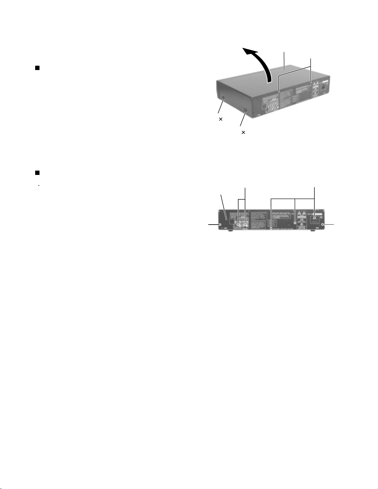
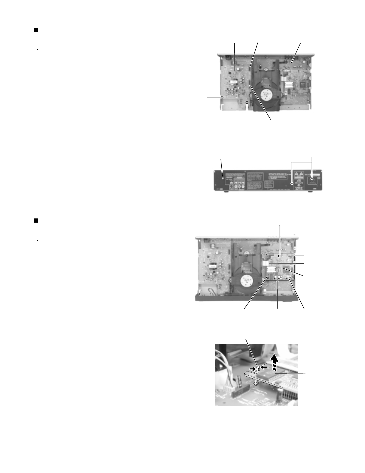
Disassembly method
XV-521BK/523GD/525BK/421BK
< Main body>
Removing the top cover (See Fig.1)
1.
Remove the four screws A on both side of the body.
2.
Remove the two screws B on the back of the body.
3.
Lift up the rear part of the top cover while pulling the
lower part of the sides, then detach upward.
Removing the rear panel (See Fig.2)
Prior to performing the following procedure, remove
the top cover.
1.
Remove the seven screws C on the back of the
body.
A
2
Rear panel
C
A
2
C
Top cover
B
Fig.1
C
C
Fig.2
1-5
Page 6
XV-521BK/523GD/525BK/421BK
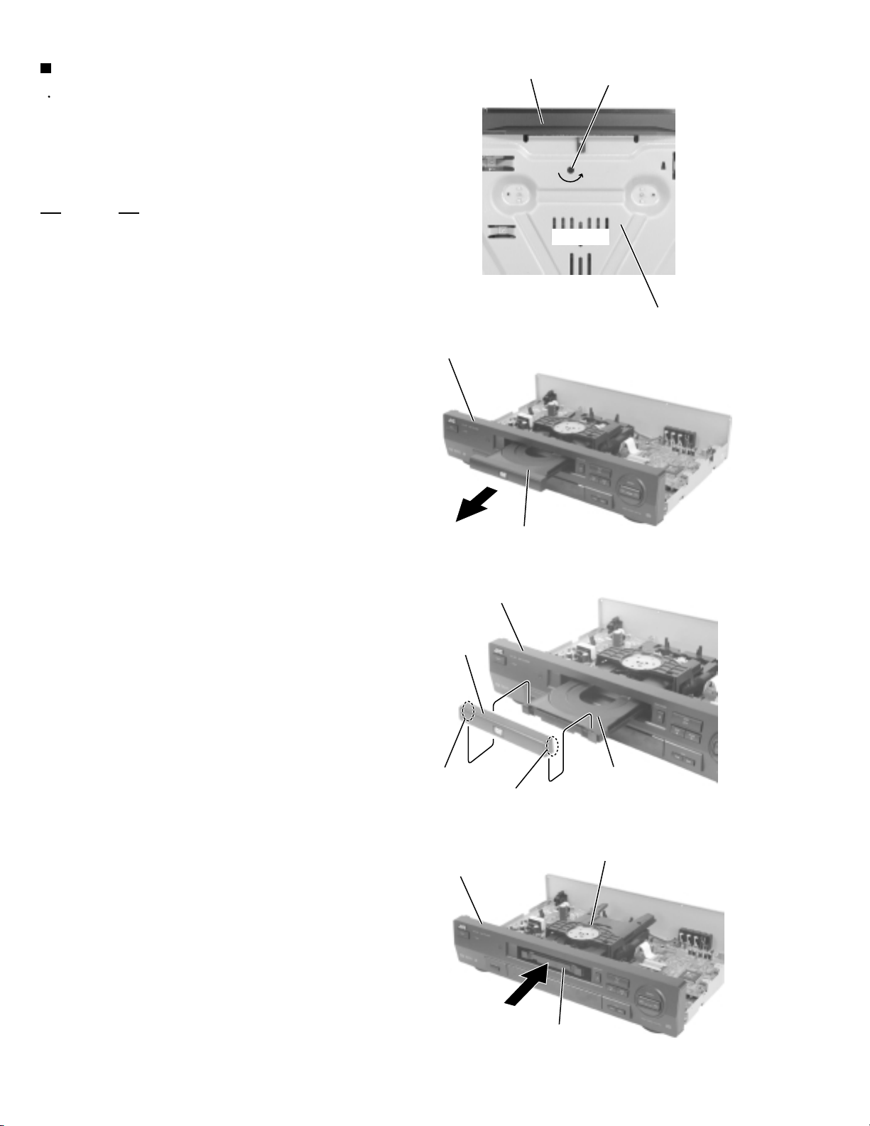
Removing the fitting (See Fig.3 to 6)
Prior to performing the following procedure, remove
the top cover.
ATTENTION:
by hand
1.
Turn over the body. Insert a screwdriver into the hole
of the bottom chassis and turnit. The loading tray will
be ejected out of the front panel assembly.
2.
Pull the loading tray toward the front.
3.
Remove the fitting upward from the loading tray at
the joints b.
4.
Push and return the loading tray.
To remove the front panel assembly
and the DVD mechanism assembly,
remove the fitting in advance.
Front panel
Front panel assembly
TRAY OPEN
(Bottom)
Fig.3
Hole
Bottom chassis
Loading tray
Front panel assembly
Fitting
Joint b
Joint b
Front panel assembly
Fig.4
Loading tray
Fig.5
DVD mechanism assembly
1-6
Loading tray
Fig.6
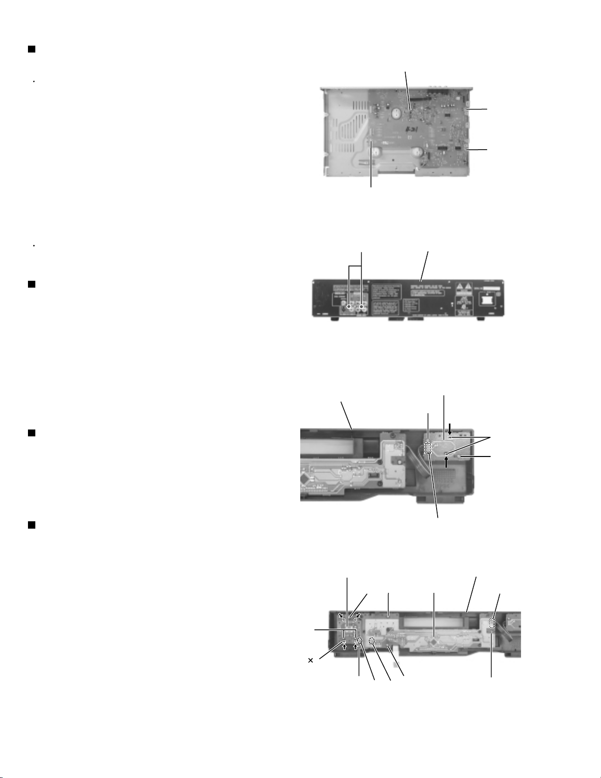
Page 7
Removing the front panel assembly
(See Fig.7 to 10)
Prior to performing the following procedure, remove
the top cover and the fitting.
1.
Disconnect the card wire from connector CN703 on
the main board.
2.
Turn over the body and remove the screw D
attaching the front panel assembly.
3.
Release the five joints c on both sides and bottom of
the body and remove the front panel assembly
toward the front.
ATTENTION:
The connector CN832 on the front
panel assembly and CN971 on the AC
jack board will be disconnected at the
same time.
AC jack board
CN971
XV-521BK/523GD/525BK/421BK
DC mechanism assembly
Main board
Front panel assembly
Fig.7
Joint c Joint c
D
CN703
Front panel assembly
Fig.8
Fig.9
Front panel assembly
Joint c
Joint c
Fig.10
1-7
Page 8
XV-521BK/523GD/525BK/421BK
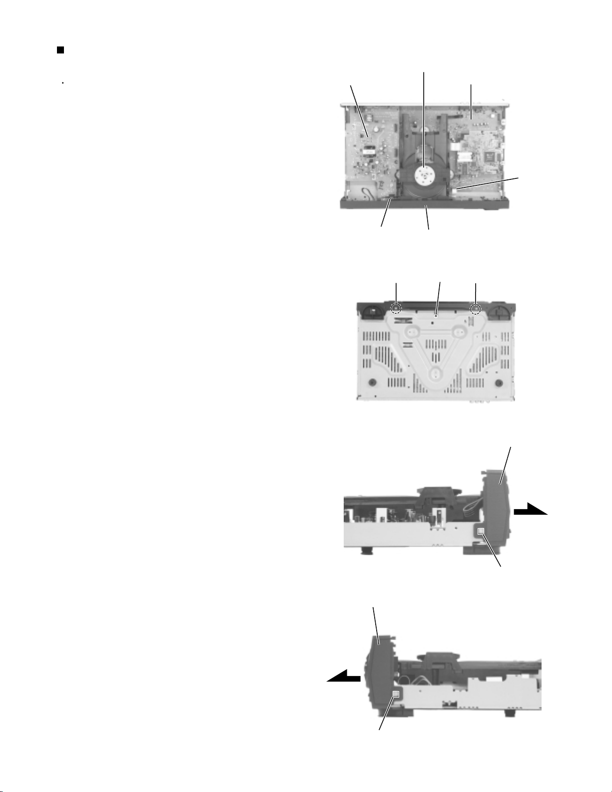
Removing the DVD mechanism assembly
(See Fig.11 to 14)
Prior to performing the following procedure, remove
the top cover and the front panel assembly.
1.
Disconnect the card wire from connector CN101 on
the DVD Servo.
2.
Disconnect the harness from connector CN031 on
the DVD mechanism assembly.
3.
Remove the screw E on the rear left part of the
loading tray.
3.
From the front side of the DVD mechanism
assembly, move the lever d in the direction of the
arrow and pull out the loading tray.
4.
Remove the two screws F on the upper side of the
DVD mechanism assembly. Then release the two
joints e and detach the clamper base back-upward.
5.
Remove the three screws G attaching the DVD
mechanism assembly.
E
Loading tray
Fig.11
Loading tray
CN101
DVD Servo
DVD mechanism assembly
P031
Lever d
P031
F
DVD mechanism assembly
Fig.12
DVD mechanism assembly
CN101
F
Joint e Joint eClamper base
Fig.13
G
CN101
1-8
G
G
DVD mechanism assembly
Fig.14
Page 9
Removing the AC jack board
(See Fig.15 and 16)
Prior to performing the following procedure, remove
the top cover and the front panel assembly.
1.
Remove the two screws H attaching the AC jack
board.
2.
Remove the two screws C on the rear panel.
3.
Disconnect connector CN951 and CN961 on the AC
jack board from CN704 and CN705 on the main
board respectively.
H
XV-521BK/523GD/525BK/421BK
CN951 / CN705
H
CN961 / CN704
Fig.15
Main boardAC jack board
Removing the DVD Servo
(See Fig.17 and 18)
Prior to performing the following procedure, remove
the top cover.
1.
Remove the screw I attaching the DVD Servo.
2.
Pull out the DVD Servo from the fix f while pinching
the fix f.
3.
Disconnect connector CN501, CN502 and CN503 on
the DVD Servo from CN601, CN701 and CN706 on
the main board respectively.
Rear panel
Fix f
C
Fig.16
CN501 / CN706
I
CN101
DVD Servo
CN503 / CN701CN502 / CN701
Fig.17
Fix f
Main board
Fig.18
DVD Servo
1-9
Page 10
XV-521BK/523GD/525BK/421BK
Removing the main board
(See Fig.19 and 20)
Prior to performing the following procedure, remove
the top cover, the front panel assembly, the DVD
mechanism assembly, the AC jack board and the
DVD Servo
1.
Remove the three screws J attaching the main
board.
2.
Remove the two screws C on the rear panel.
.
<Front panel assembly>
Main board
J
J
J
Fig.19
Prior to performing the following procedure, remove
the top cover and the front panel assembly.
Removing the power switch board
(See Fig.21)
1.
Unsolder connector FW841 on the power switch
board on the back of the front panel assembly.
2.
Remove the two screws K attaching the power
switch board.
3.
Push the two tabs g in the direction of the arrow and
remove the power switch board.
Removing the LCD board (See Fig.22)
1.
Unsolder connector FW802 and soldering h on the
LCD board.
2.
Remove the four screws L attaching the LCD board.
Removing the search switch board
(See Fig.20)
C
Fig.20
Front panel assembly
Fig.21
Rear panel
Power switch board
K
Tabs g
K
FW841
1.
Unsolder soldering i on the search switch board.
2.
Remove the three screws M.
3.
Release the four tabs j in the direction of the arrow
and remove the search switch board.
1-10
M
Tabs j 4
M
L
hi
Fig.22
Front panel assemblySearch switch board
LCD board
FW802
LLL
Page 11
XV-521BK/523GD/525BK/421BK
Disassembly method
<DVD mechanism>
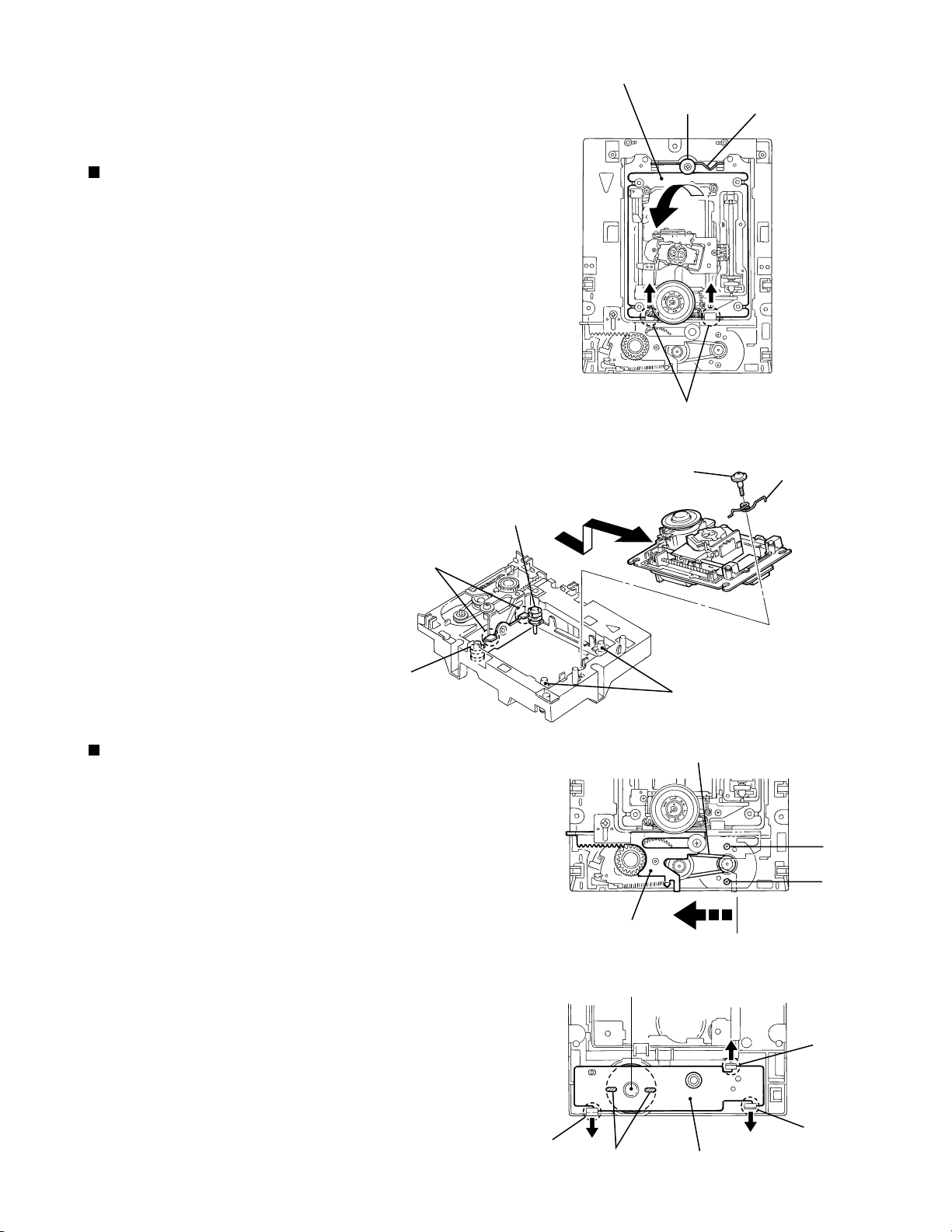
Removing the traverse mechanism unit
(See Fig.1 and 2)
1.
Remove the screw A and the spring on the upper
side of the loading base assembly.
2.
Move the rear part of the traverse mechanism unit
upward and pull backward to release the two joints a
with the base chassis.
ATTENTION:
When reattaching, engage the two
joints a and make sure the front
springs and the four insulators of the
traverse mechanism unit are correctly
attached.
Spring and Insulator
Traverse mechanism unit
A
Joints a
Fig.1
A
Spring
Spring
Joints a
Spring and Insulator
Removing the loading motor / loading
motor board (See Fig.3 and 4)
1.
Move the cam plate on the upper side of the loading
base assembly in the direction of the arrow.
2.
Remove the belt from the motor pulley.
3.
Remove the two screws B attaching the loading
motor.
4.
Turn over the loading base assembly and release the
loading motor board from the three tabs b while
spreading them outward. The loading motor board
will be detached with the loading motor.
Insulator
Fig.2
Belt
B
B
Cam plate
Fig.3
Loading motor
5.
Unsolder soldering c on the loading motor board and
remove the loading motor.
Ref.:
To remove the loading motor board only,
unsolder soldering c on the loading motor and
release the three tabs b.
Tab b
Tab b
Tab b
c
Loading motor board
Fig.4
1-11
Page 12
XV-521BK/523GD/525BK/421BK
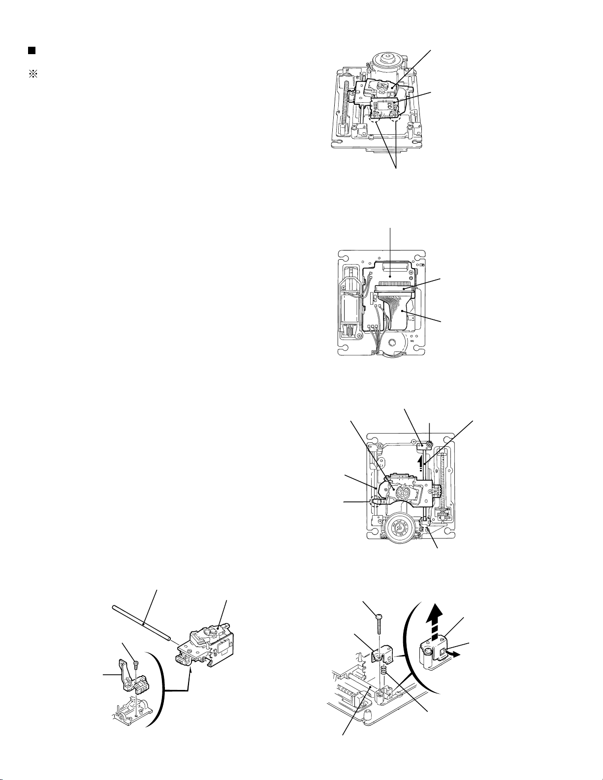
Removing the pickup (See Fig.5 to 9)
It is not necessary to remove the traverse
mechanism unit.
1.
Solder soldering d on the flexible board next to the
pickup unit.
2.
From the bottom of the traverse mechanism unit,
disconnect the flexible wire from CN10 on the pickup
board.
ATTENTION:
3.
Remove the screw C attaching the shaft stopper (R)
on the upper side of the traverse mechanism unit.
Pull the side of the shaft stopper (R) outward to
release the joint e and remove it upward. Remove
the skew spring at the same time.
4.
Move the shaft in the direction of the arrow to release
it from the part f.
Disconnecting the flexible wire without
soldering may cause damage to the
pickup.
Pickup unit
Flexible board
d
Fig.5
Pickup board
CN10
Flexible wire
5.
Release the joint g with the shaft and remove the
pickup with the shaft.
6.
Pull out the shaft.
7.
Remove the screw D attaching the switch actuator.
Shaft
Pickup
D
Pickup unit
Shaft
Joint g
Shaft stopper (R)
Fig.6
Shaft stopper (R)
Fig.7
C
C
Shaft
Part f
Shaft stopper (R)
Joint e
1-12
Switch actuator
Skew spring
Shaft
Fig.8Fig.9
Page 13

Removing the pickup board
(See Fig.5 and 10)
It is not necessary to remove the traverse
mechanism unit.
1.
Solder soldering d on the flexible board next to the
pickup unit.
2.
From the bottom of the traverse mechanism unit,
disconnect the flexible wire from CN10 on the pickup
board.
ATTENTION:
3.
Unsolder soldering h, i and j of each harness on the
pickup board.
4.
Remove the screw E attaching the pickup board and
release the two joints k.
Disconnecting the flexible wire without
soldering may cause damage to the
pickup.
Joint k
XV-521BK/523GD/525BK/421BK
Pickup unit
Flexible board
d
Fig.5
h
Pickup board
E
Removing the feed motor assembly
(See Fig.5, 10 and 11)
Prior to performing the following procedure, remove
the traverse mechanism unit.
1.
Solder soldering d on the flexible board next to the
pickup unit.
2.
From the bottom of the traverse mechanism unit,
disconnect the flexible wire from CN10 on the pickup
board.
ATTENTION:
3.
Unsolder soldering h of the motor harness on the
pickup board.
4.
Remove the two screws F attaching the feed motor
assembly and remove the thrust spring. Move the
feed motor assembly in the direction of the arrow to
pull it out from the feed holder.
Disconnecting the flexible wire without
soldering may cause damage to the
pickup.
Joint k
Feed motor assembly
Feed holder assembly
CN10
i
j
Fig.10
Feed motor assembly
Thrust spring
F
F
Fig.11
1-13
Page 14

XV-521BK/523GD/525BK/421BK
Removing the turn table assembly
(See Fig.5, 10, 12 and 13)
Prior to performing the following procedure, remove
the traverse mechanism unit.
1.
Solder soldering d on the flexible board next to the
pickup unit.
2.
From the bottom of the traverse mechanism unit,
disconnect the flexible wire from CN10 on the pickup
board.
ATTENTION:
3.
Unsolder soldering i and j of the harness extending
from the turning table assembly to the pickup board.
4.
Remove the screw G attaching the shaft stopper (F)
on the upper side of the traverse mechanism unit.
Pull the side of the shaft stopper (F) outward to
release the joint l and remove it upward. Remove the
spring at the same time.
Disconnecting the flexible wire without
soldering may cause damage to the
pickup.
Joint k
Joint k
Pickup unit
Flexible board
d
Fig.5
h
Pickup board
E
CN10
i
5.
Remove the screw H attaching the turn table
assembly.
6.
Move the turn table assembly outward and pull out
from the shaft. Then remove it from the base chassis.
Feed motor assembly
Shaft stopper (F)
Shaft stopper (F)
Joint l
G
Turn table assembly
G
Shaft stopper (F)
j
Fig.10
H
Fig.12
G
H
1-14
Shaft
Shaft
Turn table assembly
Fig.13
Page 15

XV-521BK/523GD/525BK/421BK
Main adjustment
Adjustment and confirmation matter
(1) Auto adjustment method
If microprocessor (IC401, IC402, IC714, IC716) or pick up is replaced, initialize
the DVD player in the following matter:
1. Initialize the DVD player in the following matter:
1) Make sure that no disc is on the tray.
2) Insert the power pulag to the outret while pressing "PLAY" and "OPEN/CLOSE" button at the
same time.
FL Display indicate "TEST ; Version.
3) Press Enter button. And EEPROM initialize start.
4) When indicate "96kHz EEPROM" on the display , initialize finished.
Note : During the EEPROM initialization the keys may not be operated.
Press the "POWER" key to initiate the STAND-BY mode and the test mode will then
be cancelled.
(2) Confirmation of DVD RF level
1.The oscilloscope is connected between "1"(RFOP) of
CN104 and "2"(GND).
2.Reproduction of the test disc ( VT-502)
made by JVC.
3.It is confirmed that RF LEVEL is 350mVp-p 150mVp-p.
4.When there is disorder in the waveform road cuts etc,
test disk is exchanged and measured.
(3) Confirmation of CD jitter level and RF level
1. The CD jitter meter is connected between "11"(GND)
of CN104 and "12"(FLTOUT).
The RF level is observed at the same time.
2. The first test disk(CTS-1000) made of JVC is reproduced.
3. It is confirmed that RF LEVEL is 360 100mVp-p.
5. When there is disorder in the waveform road cuts
etc, test disk is exchanged and measured.
GNDGNDFLTOUT
12 ~ 1
CN104
DVD SERVO CONTROL PWB
"1""2""11""12"
RFOP
FRONT SIDE
1-15
Page 16

XV-521BK/523GD/525BK/421BK
(4)Flap adjustment of the Pick-up guide shaft
1) Make sure that there is no disc on the tray.
2) Press both the "PLAY" and "OPEN/CLOSE" keys of the main unit to activate the primary
power and "TEST 2 D2" will be displayed on the FL indicator.
Note: If the FL indicator display stops and remains at "TEST 0", unplug the power
cord from the outlet and after waiting at least 1 second, plug it in again. After
the tray open/close procedure has completed, unplug it again and then
perform the initialization procedure again.
3) Press the "OPEN/CLOSE" key of the main unit to draw the tray out.
*Place the test disk (VT-501) on the tray and then press the "OPEN/CLOSE" key.
(Note: Pushing the tray to close it is not possible.)
4) Press the "PLAY" key of the main unit.
5) The "JIT 0000" is displayed on the FL indicator.
Set the FL indicator figure value to its minimum by adjusting the pickup guide shaft flap.
* The test mode is cancelled when the power is turned off.
Measurement
FL Display
Measurement machine
No need
General tool : Hex-head wrench(2mm)
Adjustment point
Refer to Fig.2
connections
Refer to Fig.1
Mode
Reproduction
part
Extension cord No.
QUQ605-4040AJ
Disc
VT-501
"Flap adjustment" of the Pick-up guide shaft adjusts
"Tangential adjustment machine screw" A and
"Tilt adjustment machine screw" B from the
DVD Mechanism A'ssy bottom.
1. The part at the center on the DVD test disc is
reproduced.
2.The flap adjustment screws is turned alternately
and adjusted like clearly seeing the waveform of
CN104"1" to the way.
Note
1.The tangential adjustment is done finish and,
then, tilt is adjusted.
2.The repeat the adjustment 2-3 times,for best
result.
3.The final adjustment should be tilt adjustment.
Extension Cord
DVD Mechanism A'ssy
CN11 of
Stand
Connection PWB
CN101 of DVD Servo Control PWB
DVD player
Stand
200mm
Fig.1
1-16
Page 17

XV-521BK/523GD/525BK/421BK
Confirmation after adjustment.
Confirm to reproduce video CD and CD after
the DVD test disc is adjusted and to find abnormality.
B
Fig.2
A
A
(5) About keeping the disc
As for the DVD test disc, plane accuracy is demanded.Please note the keeping place on the disc.
1. Please do not put the disc directly on the work desk etc. after uses .
2.To keep the planarity of the disc, politely handle ,and please put in a special case and keep
the disc vertically after uses .
Please keep keeping the disc in a cool place where direct sunshine and the air-conditioning
wind do not drive.
3.When the disc curves,an accurate adjustment cannot be done.
Please exchange for a new test disc and adjust optics.
4 Other discs might not be able to be reproduced when adjusting on a curved disc.
Point of adjustment
* Please execute the static electricity protection measures before starting the
adjustment.
* When the following parts are exchanged,optical adjustment "Adjust the flap of the disc motor"
is necessary.
1.The disc motor was exchanged.
2.The laser pick up was exchanged.
3.The traverse motor unit was exchanged.
Note
Additionally, please adjust the flap of the disc motor when the picture quality deterioration is
seen .The basic adjustment though, is unnecessary for part exchange in the traverse.
An optical adjustment in the laser pick up cannot be done.
Please adjust the flap of the disc motor after exchanging the laser pick up.
* When the traverse unit is exchanged, the adjustment is basically unnecessary.
1-17
Page 18

XV-521BK/523GD/525BK/421BK
Check points for each error
(1) Spindle start error
*Defective spindle motor
Are there 10ohms resistance between each pin of CN101 "29~31"?
(The power supply is turned off and measured.)
*Hall element: Is sine wave output between CN101 "23" and "24", between "25" and "26",
and between "27" and "28" during rotation?
In either case, replace the mechanical unit.
*Defective spindle driver (IC251)
Is a driving wave output from CN101 "29~31" ?
During
rotation
Is IC251 "9" at "H" level (START)?
Servo IC --- Is control signal sent to the motor driver ?
IC201 "95" : Duty is 50% during stop, but varies during rotation (greatly varies at start).
--- If not sent, pattern or servo IC (IC201) is defective.
R259 : approx 2.5V during stop, but varies during rotation (greatly varies at start).
--- of not sent, pattern or servo IC (IC201) is defective.
Is FG input to servo IC ?
Observe FG wave from IC201 "89". --- If not output, pattern, IC251 or IC201 is defective.
(2) Disc Detection, Distinction error (no disc, no REFNV)
* Laser is defective.
* Front End Processor is defective (IC101).
* APC circuit is defective. --- Q101.
* Pattern is defective. --- Lines for CN101 "15" and "17".
Lines for between IC201 "2" and IC101 "2"(LDONA),
between IC201 "3" and IC101 "1" (LDONB).
* Servo IC is defective (IC201).
* Is signal sent to IC201(servo)"71" AS2 ?
* IC101 --- For signal from IC101 to IC301, is signal output from IC101 "88" (RFAS1) and
IC101 "69" REENV ?
1-18
Page 19

XV-521BK/523GD/525BK/421BK
(3) Traverse movement NG
* For automatic adjustment, traverse movement occurs only when the position is changed to retry
judging the disc type after the 1st judgment resulted in an error. Therefore, traverse movement
rarely occurs because, in most cases, disc judgment at the current position (1st time judgment)
is executed successfully. (Of course, NG rarely occurs in this step.)
Note: 1st time judgment of disc type resulted in NG. --- The re-judgment of disc type may not be
successful. Therefore, after removing the cause of traverse movement, re-execute automatic
adjustment and confirm that no problem exists.
* Check point
a) During stop
Whether 50% duty pulse is output to R273
Whether between R274 and C271 is at approx. 2.5VDC
Offset voltage between CN101 "34" and "35" (scores mV if exists)
b) When tray is opened or closed
Check by oscilloscope whether a rectangular wave signal is output from CN101 "34" or "35".
50msec
2.5V
Approx.
500mV
GND
If checking a) or b) resulted in NG, IC201 maybe defective.
(4) Focus ON NG
* Is FE output ? --- Pattern, IC101
* Is FCDRV signal sent ? (R286) --- Pattern, IC301
* Is driving voltage sent ?
CN101 "20", "21" --- If NG, pattern, driver, mechanical unit (with the power turned off, measure the
resistance between CN101 "20" and "21").
* Does CN101 "7"(SRF1) become "H" and is the focus drawing in done?
--- Mechanical unit (laser power too low), IC101(defective gain)
--- Moreover, It is thought that abnormality is found in the disk.
* Mechanical unit is defective.
(5) Tracking ON NG
* When the tracking loop cannot be drawn in, IC201 "39" (/TRON) does not become "L".
* Mechanical unit is defective.
Because the undermentioned adjustment value is abnormal, it is not possible to draw in normally.
* Periphery of driver (IC271)
Constant or IC it self is defective.
(When passing without becoming abnormal while adjusting the following.)
* Servo IC (IC201)
When improperly adjusted due to defective IC.
[Focus position rough adjustment]
[Phase difference cancellation rough adjustment]
[Tracking balance adjustment]
1-19
Page 20

XV-521BK/523GD/525BK/421BK
(6) Spindle CLV NG
* When the spindle cannot be shifted to CLV Servo, does not become "H" between IC301 "69"
and IC201"37".
* IC201 Is signal output from CN103 "1" (RFOP)?
* IC201 Is signal output from CN103 "11" (DSLIP)?
* IC201 Is signal output from CN103 "6" to "9" (binary-coded clock and data)?
* IC201 Is "39" (/TRON) at "L" level ?
* IC301 "74" to "76" --- Is signal output to IC201 "24", "25", "28" (In case of only CD).
(Serial communication of rotation information)
* Spindle motor driver is defective.
Even when one of the three phases is defective, item (1) may be passed.
--- Check the second item in (1) above.
* C260 to C263 Defective soldering
If noise eliminating capacitors are not properly soldered, noise may ride on the waveform.
* Besides, the undermentioned cause is thought though specific of the cause is difficult because various
factors are thought.
Mechanism is defective.(jitter)
IC101, IC201.
(7) Address read NG
* Besides, the undermentioned cause is thought though specific of the cause is difficult because various
factors are thought.
Mechanism is defective. (jitter)
IC201, IC301, IC401.
The disc is dirty or the wound has adhered.
(8) Between layers jump NG (double-layer disc only)
* When the focus flight is generated when jumps between layers.
Because all adjustments for L1 layer must be successful, this error may rarely be due to a
circuit defect.
* Crosstalk might occur from tracking to focus system. (See (11) ) --- Replace the mechanical unit.
* Driver surroundings.
* Defect of constant and IC.
* For double-layer discs, after checking CLV on layer L1, jumps to layer L0 after mode changes to FG.
Then tracking is turned off, and adjustments are executed from the focus position coarse adjustment
in order.
* When the jump between layers is done on the single-layer disk, the disk distinction error is thought.
--- The laser power is low (RF level is confirmed by CN102 "1" (RFOP)).
--- AS1, AS2, REFNV Is the signal sent to between IC101 and IC201 ?
1-20
Page 21

(9) Neither picture nor sound is output
* Cannot search
a) Can the feed system be driven?
Check the waveform of TRSDRV signal (R273). --- Waveform between R274 and C271.
Search results in a change of duty
(three values with 2.5V at the center)
(The figure is exaggerated.)
Check the waveform of CN101 "1" and "2". --- After the driver (IC271)
XV-521BK/523GD/525BK/421BK
b) Is kick available?
Check the TRDRV signal waveform from R289.
Check the waveform of CN101 "22" and "23" --- After the driver (IC271)
Although differs in amplitude and DC offset, the waveform is similar to that of R289
Kick pulse
Approx.
2.5V
Long-distance seek
Acceleration pulse at start;
deceleration pulse at stop
(each one)
(In the direction of search,
opposite to this figure)
For short-distance search, the waveform
becomes roundish, not trapezoidal, and
voltage is low.
Feed
Tracking
Kick pulse (fine seek) is
inserted after longdistance seek.
(Not one)
Hold (DC) during feed
1-21
Page 22

XV-521BK/523GD/525BK/421BK
(10) Picture is distorted or abnormal sound occurs at intervals of several seconds.
Does JITOUT
change periodically?
(2V or more in peak
value, except
during kick)
YES
Feed system is defective (drive gain is defective: too large).
Check the waveform according to a) in (9).
Play back a simple disc with no angle change.
OK when the following waveform appears at intervals
of several seconds.
5~10Sec.
1~1.2V
Some system other
NO
than servo may be
defective.
If this voltage is too
high (2V or more, for
example), feed motor
may be defective, or
the mechanical unit
has seized.
(11) Others (unusual events experienced to date)
* Problem occurs with double-layer discs although no problem occurs with single-layer DVD.
(Error occurs, or search becomes unstable and takes longer.)
Crosstalk might occur from tracking to focus system.
--- When FE was observed during search (skip, etc.), it was found that a wave resembling TE
with an amplitude of 200mVp-p was riding on FE.
--- Mechanical unit was replaced.
* Error frequently occurred in the outer part of discs although no error occurred in the inner part.
--- Mechanical unit was replaced because tilt seemed to be defective.
(12) CD During normal playback operation
a) Is TOC reading normal?
NO
Please refer to "Servo Volume" flow.
Displays total time
for CD-DA.
Shifts to double-speed
mode for V-CD.
YES
NO
b)Playback possible?
*--:-- is displayed during FL serch.
According to [*Cannot serch ] for DVD(9), check the feed
and tracking systems.
*No sound is output although the time is displayed.(CA-DA)
*DAC, etc, other than servo.
*The passage of time is not stable, or picture is abnormal.(V-CD)
*The wound of the disc and dirt are confirmed.
(13) Others
V-CD : Frequent occurrence of error in inside and outer.
(Even the disk without the wound : when generated.)
Waveform observation
--- Is the oscillation frequency of about 700~900Hz output?
(Borrow a pertinent disk for the complaint for the combination with the disk.)
--- Exchanges mechanism for the mechanism resonance.
1-22
Page 23

XV-521BK/523GD/525BK/421BK
Precautions for Service
Handling of Traverse Unit and Laser Pickup
1. Do not touch any peripheral element of the pickup or the actuator.
2. The traverse unit and the pickup are precision devices and therefore must not be subjected to
strong shock.
3. Do not use a tester to examine the laser diode. (The diode can easily be destroyed by the
internal power supply of the tester.)
4. To replace the traverse unit, pull out the metal short pin for protection from charging.
5. When replacing the pickup, after mounting a new pickup, remove the solder on the short land
which is provided at the center of the flexible wire to open the circuit.
6. Half-fixed resistors for laser power adjustment are adjusted in pairs at shipment to match the
characteristics of the optical block.
Do not change the setting of these half-fixed resistors for laser power adjustment.
Destruction of Traverse Unit and Laser Pickup by Static Electricity
Laser diodes are easily destroyed by static electricity charged on clothing
or the human body. Before repairing peripheral elements of the traverse
unit or pickup, be sure to take the following electrostatic protection:
1. Wear an antistatic wrist wrap.
2. With a conductive sheet or a steel plate on the workbench on which
the traverse unit or the pick up is to be repaired, ground the sheet
or the plate.
3. After removing the flexible wire from the connector (CN101),
short-circuit the flexible wire by the metal clip.
4. Short-circuit the laser diode by soldering the land which is provided
at the center of the flexible wire for the pickup.
After completing the repair, remove the solder
to open the circuit.
Short-circuit
1-23
Page 24

XV-521BK/523GD/525BK/421BK
Description of major ICs
AK93C45AF-W (IC791) : CMOS EEPROM
1.Pin Layout
AK93C45AF
NC
YCC
CS
SK
1
2
3
4
2.Pin Functions
Symbol
CS
SK
DI
DO
Vcc
GND
NC
NC
8
GND
7
DO
6
DI
5
Function
Chip Select
Serial Clock Input
Serial Data Input
Serial Data Output
Power Supply
Ground
Non connection
3.Block Diagram
DI
INSTRUCTION
REGISTER
CS
SK
INSTRUCTION
DECODE.
CONTROL
AND
CLOCK
GENERATION
DATA
REGISTER
ADD.
BUFFERS
16
VREF
R/W AMPS
AND
AUTO ERASE
DECODER
VPP SW
GENERATOR
VPP
16
DO
EEPROM
1024bit
64 X 16
1-24
Page 25

AK93C65AF-X (IC403) : EEPROM
1.Terminal layout
XV-521BK/523GD/525BK/421BK
PE
VCC
CS
SK
2.Block diagram
DI
CS
INSTRUCTION
1
2
3
4
8 PIN SOP
REGISTER
8
7
6
5
INSTRUCTION
GENERATION
NC
GND
DO
DI
DECODE,
CONTROL
AND
CLOCK
DATA
REGISTER
ADD.
BUFFERS
16
R/W AMPS
AND
AUTO ERASE
DECODER
DO
16
EEPROM
4096bit
256 x 16
SK
PE
3.Pin function
Pin no. Symbol
1 PE
2 VCC
3 CS
4 SK
5 DI
6 DO
7 GND
8 NC
Function
Program enable (With built-in pull-up resistor)
Power supply
Chip selection
Cereal clock input
Cereal data input
Cereal data output
Ground
No connection
NOTE : The pull-up resistor of the PE pin is about 2.5M (VCC=5V)
VREF
VPP SW
VPP
GENERATOR
1-25
Page 26

XV-521BK/523GD/525BK/421BK
HY57V161610DTC8 or KM416S1120DT-G8 (IC504,IC505) : 16MB SDRAM
1.Block diagram
CLK
CKE
Address
CS
RAS
CAS
WE
Clock
Generator
Mode
register
Command decoder
Control logic
Row
address
buffer &
Refresh
counter
Column
address
buffer &
burst
counter
Bank B
Bank A
Row decoder
Sense amplifier
Column decoder
& latch circuit
Data counter
Input & output
Latch circuit
DQM
DQ
buffer
2.Pin function
Pin No. Symbol Description Pin No. Symbol Description
1
2,3
4
5,6
7
8,9
10
11,12
13
14
15
16
17
18
19,20
21~24
25
VCC
DQ0,1
VSS
DQ2,3
VDD
DQ4,5
VSS
DQ6,7
VCC
LDQM
WE
CAS
RAS
CS
A11,10
A0~3
VCC
Power supply
Data input/output
Connect to GND
Data input/output
Power supply
Data input/output
Connect to GND
Data input/output
Power supply
Lower DQ mask enable
Write enable
Column address strobe
Row address strobe
Chip enable
Address inputs
Address inputs
Power supply
26
27~32
33
34
35
36
37
38
39,40
41
42,43
44
45,46
47
48,49
50
VSS
A4~9
NC
CKE
CLK
UDQM
NC
VCC
DQ8,9
VSS
DQ10,11
VDD
DQ12,13
VSS
DQ14,15
VSS
Connect to GND
Address inputs
Non connect
Clock enable
System clock input
Upper DQ mask enable
Non connect
Power supply
Data input/output
Connect to GND
Data input/output
Power supply
Data input/output
Connect to GND
Data input/output
Connect to GND
1-26
Page 27

XV-521BK/523GD/525BK/421BK
MC44724AVFU (IC554) : VIDEO ENCODER
1.Terminal layout 2.Block diagrams
1
~
16
17 ~ 32
3.Pin function
No. Symbol
1
CVBS/Cb/B1
2
CVBS/Cb/B1
3
CVBS/Cb/B1Vdd
4
Y/G1
5
Y/G1
6
Y/G1/Vdd
7
C/Cr/R1
8
C/Cr/R1
9
C/Cr/R1Vdd
10
DAVss
11
TBIAS1
12
Vref1
13
DAVdd
14
Vref2
15
TBIAS2
16
NC
17
CVBS/Cb/B2
18
CVBS/Cb/B2
19
CVBS/Cb/B2Vdd
20
Y/G2
21
Y/G2
22
Y/GVdd
23
C/Cr/R2
24
C/Cr/R2
25
C/Cr/R2Vdd
26
ChipA
27
TEST
28
DVdd
29
CLOCK
30
DVss
31
Reset
32
PAL/NTSC
64 ~ 49
I/O
48
~
33
O
Analog composite drive signal (+)
O
Analog composite drive signal (-)
-
Power supply for CVBS/Cb/B DAC1
O
Analog brightness signal/G drive signal (+)
O
Analog brightness signal/G drive signal (-)
-
Power supply for Y/G DAC
O
Analog chroma signal (+)
O
Analog chroma signal (-)
-
Power supply for C/Cr/RDAC
-
Connect to ground for DAC
O
Standard BIAS for DAC1
-
Standard voltage for DAC1
-
Power supply for DAC
-
Standard voltage for DAC2
O
Standard BIAS for DAC2
-
Non connect
O
Analog composite drive signal (+)
O
Analog composite drive signal (-)
-
Power supply for CVBS/Cb/B DAC2
O
Analog brightness signal/G drive signal (+)
O
Analog brightness signal/G drive signal (-)
-
Power supply for Y/G DAC
O
Analog chroma signal (+)
O
Analog chroma signal (-)
-
Power supply for C/Cr/RDAC2
-
Chip address selection
I
Connect to test pin
-
Digital ground
I
Clock signal input (27MHz)
-
Power supply for digital circuit
I
Reset signal input L:ON
I
Selection NTSC/PAL NTSC:L PAL:H
ChipA
DVdd
DVdd
DVss
DVss
DVIN[7:0]
TP[8:1]
TVIN
TP[0]IN
Clock
Reset
PAL/NTSC
Function
H.V
DEMAX
Y
cb
cr
12C / SPI
SO
SDA/SI
EXT
Sync_ generator
CGMS,
wss gen
0
off_set
0
0
sub carrier
SEL
SCL/SCK
No. Symbol
33
34
35
36
37
38
39
40
41
42
43
44
45
46
47
48
49
50
51
52
53
54
55
56
57
58
59
60
61
62
63
64
F/Vsync
CCwss gen
Modulator
gen
SO
SDA/SI
SCL/SCK
SEL
DVdd
DVss
DVIN7
DVIN6
DVIN5
DVIN4
DVIN3
DVIN2
DVIN1
DVIN0
TVIN
EXT
F/Vsyac
Chsyac
DATST
TP-8
TP7
TP6
TP5
DVss
DVdd
TP4
TP3
TP2
TP1
TP0
DLVdd
DLVss
Hsync
RGB
matrix
Y/G2Vdd
C/Cr/R2Vdd
CVBS/Cb/B2Vdd
Copy,
protection
bus
0
+
0
+
0
0
0
0
DAC BIAS DAC DAC DAC
DAC
Output Selector
DAC
BIAS
TEST
TEST
I/O
-
Non connect
I
SPI Mode : Serial data input
I
Serial clock input
I
Power supply for serial data,chip select,digital
--
Power supply for digital circuit
--
Digital ground
I/O
Y data input / test data I/O
I/O
Y data input / test data I/O
I/O
Y data input / test data I/O
I/O
Y data input / test data I/O
I/O
Y data input / test data I/O
I/O
Y data input / test data I/O
I/O
Y data input / test data I/O
I/O
Y data input / test data I/O
I
VIDEO mute on Reset(0:nomal, 1:mute)
I/O
Frame output / VBI information input
I/O
Frame / Vertical, synchronous I/O
I/O
The horizontal, synchronous I/O
I
Data input
I/O
Multiplex data input
I/O
Multiplex data input
I/O
Multiplex data input
I/O
Multiplex data input
-
Ground for digital circuit
-
Power supply for digital circuit
I/O
Data input / Test data I/O
I/O
Data input / Test data I/O
I/O
Data input / Test data I/O
I/O
Data input / Test data I/O
I/O
Data input / Test data I/O
-
Power supply for D/A converter
-
Ground for D/A converter
DLVss
DLVdd
Function
Y/G1Vdd
CVBS/Cb/B1Vdd
C/Cr/R1Vdd
Y/G1
Y/G1
CVBS/Cb/B1
CVBS/Cb/B1
C/Cr/R1
C/Cr/R1
Vref1
iBIAS1
Y/G2
Y/G2
CVBS/Cb/B2
CVBS/Cb/B2
C/Cr/R2
C/Cr/R2
Vref2
Ibias
DAVdd
DAVss
1-27
Page 28

XV-521BK/523GD/525BK/421BK
MN101C12GCS3 (IC701) : System micom
1.Terminal layout
100 ~ 76
25
2.Pin function
Pin No. Symbol I/O Function
1
2
3
4
5
6
7
8
9
10
11
12
13
14
15
16
17
18
19
20
21
22
23
24
25
26
27
28
29
30
31
32
33
34
35
36
37
38
1
~
26 ~ 50
GND
CS0
CS1
CS2
NTSEL
POWER SW
SHUT1
KEY1-5
KEY6-10
VREF
VDD
OSC2
OSC1
VSS
XI
XO
MMOD
OSDCS3
RSTE
OSDDO
S2UDT
U2SDT
SCLK
BUSY
CPURST
REQ
REMO
CS3
-
-
NC
RESET
NC
NC
VDD
OSDCK
NT
75
~
51
-
-
-
O
-
O
O
O
O
O
O
O
O
O
O
O
O
GND
I
A set bit0 (It is effective in the U.E version)
I
A set bit1 (It is effective in the U.E version)
I
A set bit2 (It is effective in the U.E version)
I
NTSC/PAL switch SW input
I
Power key input
I
JOG shuttle inout (AD)
I
10 Key input (1~5)
I
10 Key input (6~10, +10)
+B (Apply 5V)
+B (Apply 5V)
10MHz OSC
I
10MHz OSC
GND
I
Unused, Connects with GND
Unused
I
Connects with GND
VENCODER chip selection
V.ENCOSER reset
V.ENCODER communication DATA
Communication between unit microcomputers DATA OUT
I
Communication between unit microcomputers DATA IN
Communication between unit microcomputers CLK
Communication between unit microcomputers BUSY
Unit microcomputer reset
I
Communication between unit microcomputers REQ
I
Remote control interruption
I
Set password change judgment bit(H:Change, L:Usual)
I
GND
I
H:Checkers mode, L:Normal mode
I
H:Running mode, L:Normal mode
I
Un used
I
Reset input
Un uesd
Un used
Un used
V.ENCODER communication CK
1-28
Page 29

Pin No. Symbol I/O Function
XV-521BK/523GD/525BK/421BK
MN101C12GCS3 (2/2)
39
40
41
42
43
44
45
46
47
48
49
50
51
52
53
54
55
56
57
58
59
60
61
62
63
64
65
66~76
77
78
79
80
81~85
86
87
88
89
90
91
92
93
94
95
96
97
98
99
100
FS2
CHREQ
CHST
CHDATAIO
NC
CHCK
FLDATAO
FLDATAI
FLCK
FLCS
FLRST
EEDO
EEDI
EECK
EECS
VS1
VS3
DMUT1
DMUT2
PDB2
PDB1
DEMP2
DEMP1
DENA
KARAOKE
POWERON
VS2
NC
AVC I
AVC O
NC
STANBYIND
NC
CS4
MA
MB
M1M3
MD
MC
GAIN2
GAIN1
HPMUT
DAVSS
LMUTE
CMUTE
SMUTE
MUTE
DAVDD
O
O
O
O
O
I
O
O
O
O
I
O
O
O
O
-
-
-
-
-
-
O
O
O
O
I
O
O
O
O
O
O
O
O
O
O
-
-
O
O
O
O
O
-
48kHz, 96kHz switch
I
Changer communication REQUEST
Changer communication STROBE
Changer communication DATAI/O
Changer communication CLOCK
FL driver communication DATAO
FL driver communication DATAI
FL driver communication CLOCK
FL driver communication CS
FL reset output
EEPROM communication DATAO
EEPROM communication DATAI
EEPROM communication CLOCK
EEPROM communication CS
S1 control
S3 control(STBY:H, P.ON:L)
Un used
Un used
Un used
Un used
Un used
Un used
Un used
KARAOKE gain control(At KARAOKE : H)
Power ON output
S2 control
Un used
AV COMPULINK input
AV COMPULINK output
Un used
Standby LED output
Un used
Un used
DAC control MA
DAC control MB
DAC control M1M3
DAC control MD
DAC control MC
Un used
Un used
Un used
Un used
Un used
Un used
Un used
Front mute output
Apply 5V
1-29
Page 30

XV-521BK/523GD/525BK/421BK
NJM4580D (IC672) : LPF, Mic and H.phone Amp.
1.Terminal layout
2.Block diagram
+
V
INPUT
+
A OUT
A -IN
A +IN
V
1
2
A
3
-
4
(TOP VIEW)
B
8
7
6
5
+
V
B OUT
B -IN
B +IN
-
V
IC-PST9140-T (IC717) : Reset IC
1. Block diagram
CO1
OUTPUT
VCC
2
OUT
1
OP1
1-30
GND
3
Page 31

NJM78M05FA (IC718) : Regulator
1. Terminal layout
2. Block diagram
XV-521BK/523GD/525BK/421BK
1-31
Page 32

XV-521BK/523GD/525BK/421BK
STR-G6651 (IC901) : Switch regulator
VIN
4
D
START
REG
T. S. D
O.V.P
LATCH
O.S.C
Comp.2
Vth(2)
DRIVE
Comp.1
2
S
Vth(1)
5
O.C.P/F.B
3
GND
1-32
Page 33

TC74VHC00FT-X (IC503) : Wright timing control
1
5
4
2
3
VCC
OUT Y
IN B
IN A
GND
TC7SH08FU-X (IC311) : Timing control
1.Terminal layout
1.Terminal layout
2.Block diagram
1
2
3
4
8
7
6
5
VCC
PR
CLR
Q
CK
D
Q
GND
TC7WH74FU-X (IC374) : Clock buffer
1.Terminal layout / Block diagram
Vcc 4B 4A 4Y 3B 3A 3Y
14 13
12
11 10 9 8
XV-521BK/523GD/525BK/421BK
2
1
1A 1B 1Y 2A 2B 2Y GND
6
543
7
TC7SH32FU-X (IC312) : Timing control
1.Terminal layout
IN B
IN A
GND
1
2
3
5
4
VCC
OUT Y
1-33
Page 34

XV-521BK/523GD/525BK/421BK
ZIVA3-PE0 (IC501) : AV Decoder
Pin No.
1
2
3
4
5
6
7
8
9
10
11
12
13
14
15
16
17
18
19
20
21
22
23
24
25
26
27
28
29
30
31
32
33
34
35
36
37
38
39
40
41
42
Symbol
PIO0
H DATA 0
H DATA 1
H DATA 2
VDD-3.3
H DATA 3
VSS
H DATA 4
H DATA 5
H DATA 6
H DATA 7
VDD-2.5
RESET
VSS
WAIT/DTACK
INT
VDD-3.3
NC
VSS
NC
PIO11
PIO12
PIO13
PIO14
PIO15
PIO16
VDD-3.3
PIO17
VSS
PIO18
PIO19
PIO20
PIO21
PIO22
PIO23
VDD-3.3
PIO24
VSS
PIO25
VDD-2.5
PIO26
VSS
I/O
I/O
I/O
I/O
I/O
O
O
O
O
I/O
I/O
I/O
I/O
I/O
I/O
I/O
Programmable I/O pins.Input mode after reset.
8-bit bi-derectional host data bus. writes data to the decoder Code FIFO via HDATA.
MSB of the 32-bit word is written first. The host also reads and writes the decoder
internal registers and local SDRAM via HDATA.
3.3-V supply voltage for I/O signals.
8-bit bi-derectional host data bus. writes data to the decoder Code FIFO via HDATA.
MSB of the 32-bit word is written first. The host also reads and writes the decoder
internal registers and local SDRAM via HDATA.
Ground for core logic and I/O signals.
8-bit bi-derectional host data bus. writes data to the decoder Code FIFO via HDATA.
MSB of the 32-bit word is written first. The host also reads and writes the decoder
internal registers and local SDRAM via HDATA.
2.5-V supply voltage for core logic.
Hardware reset. An external device asserts RESET(active LOW) to execute a decoder
I
hardware reset. To ensure proper initialization after power is stable,assert RESET for at
least 20 ms.
Ground for core logic and I/O signals.
Transfer not complate / data acknowledge. Active LOW to indicate host initiated transfer
is not complate.WAIT is asserted after the falling edge of CS and reasserted when
decoder is ready to complate transfer cycle. Open drain signal, must be pulled-up via
1kW to 3.3 volts. Driven high for 10 ns before tristate.
Host interrupt. Open drain signal, must be pulled-up via 4.7kW to 3.3 volts.
Driven high for 10 ns before tristate.
3.3-V supply voltage for I/O signals.
No Connection
Ground for core logic and I/O signals.
No Connection
Programmable I/O pins. Input mode after reset
3.3-V supply voltage for I/O signals.
Programmable I/O pins. Input mode after reset
Ground for core logic and I/O signals.
Programmable I/O pins. Input mode after reset
Programmable I/O pins. Output mode after reset
3.3-V supply voltage for I/O signals.
Programmable I/O pins. Output mode after reset
Ground for core logic and I/O signals.
Programmable I/O pins. Output mode after reset
2.5-V supply voltage for core logic.
Programmable I/O pins. Output mode after reset
Ground for core logic and I/O signals.
-
ZIVA3-PEO (1/5)
Function
1-34
Page 35

Pin No.
44
45
46
47
48
49
50
51
52
53
54
55
56
57
58
59
60
61
62
63
64
65
66
67
68
69
70
71
72
73
74
75
76
77
78
79
80
81
82
83
84
85
86
87
88
89
90
91
92
93
94
95
96
97
98
Symbol
PIO28
PIO29
PIO30
VDD-3.3
PIO31
VSS
NC
PIO1
MDATA15
M DATA 0
VDD-3.3
MDATA14
VSS
M DATA 1
MDATA13
M DATA 2
VDD-3.3
MDATA12
VSS
M DATA 3
VDD-2.5
MDATA11
VSS
M DATA 4
VDD-3.3
MDATA10
VSS
M DATA 5
M DATA 9
M DATA 6
VDD-3.3
M DATA 8
VSS
M DATA 7
LDQM
UDQM
VDD-3.3
MWE
VSS
SD-CLK
SD-CAS
SD-RAS
VDD-3.3
SD-CS1
VSS
SD-CS0
VDD-2.5
NC
VSS
NC
VDD-3.3
MADDR9
VSS
MADDR11
XV-521BK/523GD/525BK/421BK
I/O
I/O
Programmable I/O pins. Output mode after reset
-
3.3-V supply voltage for I/O signals.
I/O
Programmable I/O pins. Output mode after reset
-
Ground for core logic and I/O signals.
O
No Connection
Programmable I/O pins. Input mode after reset
I/O
Memory data
I/O
Memory data
I/O
3.3-V supply voltage for I/O signals.
Memory data.
I/O
Ground for core logic and I/O signals.
-
Memory data.
I/O
3.3-V supply voltage for I/O signals.
Memory data.
I/O
Ground for core logic and I/O signals.
Memory data.
I/O
2.5-V supply voltage for core logic.
Memory data.
I/O
Ground for core logic and I/O signals.
Memory data.
I/O
3.3-V supply voltage for I/O signals.
Memory data.
I/O
Ground for core logic and I/O signals.
-
Memory data.
I/O
3.3-V supply voltage for I/O signals.
Memory data.
I/O
Ground for core logic and I/O signals.
Memory data.
I/O
SDRAM LDQM.
O
SDRAM UDQM.
O
3.3-V supply voltage for I/O signals.
SDRAM write enable. Decoder asserts active LOW to request a write operation to the
O
SDRAM array.
Ground for core logic and I/O signals.
SDRAM system clock.
O
Active LOW SDRAM column address.
O
Active LOW SDRAM row address.
O
3.3-V supply voltage for I/o signals.
Active LOW SDRAM bank select.
O
Ground for core logic and I/O signals.
Active LOW SDRAM bank select.
O
2.5-V supply voltage for core logic.
No Connection.
O
Ground for core logic and I/O signals.
No Connection.
O
3.3-V supply voltage for I/O signals.
Memory address.
O
Ground for core logic and I/O signals.
Memory address.
O
Function
ZIVA3-PEO (2/5)
1-35
Page 36

XV-521BK/523GD/525BK/421BK
Pin No.
99
100
101
102
103
104
105
106
107
108
109
110
111
112
113
114
115
116
117
118
119
120
121
122
123
124
125
126
127
128
129
130
131
132
133
134
135
136
137
138
139
140
141
142
143
144
145
146
147
148
Symbol
MADDR8
MADDR10
VDD-3.3
MADDR7
VSS
MADDR0
MADDR6
MADDR1
VDD-3.3
MADDR5
VSS
MADDR2
MADDR4
MADDR3
VDD-3.3
NC
VSS
NC
VDD-2.5
NC
VSS
NC
VDD-3.3
NC
VSS
NC
RESERVED
PIO2
NC
RESERVED
PIO3
VDD-3.3
RESERVED
VSS
RESERVED
PIO4
RESERVED
PIO5
V DATA 0
V DATA 1
VDD-2.5
V DATA 2
VSS
PIO6
V DATA 3
I/O
O
-
O
-
O
-
O
-
O
-
O
-
O
-
O
-
O
-
O
-
O
O
I/O
O
I
I/O
I
I
I/O
I
I/O
O
-
O
-
I/O
O
Memory address.
3.3-V supply voltage for I/O signals.
Memory address.
Ground for core logic and I/O signals.
Memory address.
3.3-V supply voltage for I/O signals.
Memory address.
Ground for core logic and I/O signals.
Memory address.
3.3-V supply voltage for I/O signals.
No Connection
Ground for core logic and I/O signals.
No Connection
2.5-V supply voltage for core logic.
No Connection
Ground for core logic and I/O signals.
No Connection
3.3-V supply voltage for I/O signals.
No Connection
Ground for core logic and I/O signals.
No Connection
Open drain signal, must be pulled-up via 4.7kW to 3.3 volts.
Programmable I/O pins. Input mode after reset.
No Connection
Tie to VSS or VDD-3.3
Programmable I/O pins. Input mode after reset.
3.3-V supply voltage for I/O signals.
Tie to VSS or VDD-3.3
Ground for core logic and I/O signals.
Tie to VSS or VDD-3.3
Programmable I/O pins. Input mode after reset.
Tie to VSS or VDD-3.3
Programmable I/O pins.Input mode after reset.
Video data bus. Byte serial CbYCrY data synchronous with VCLK. At power-up,
the decoder does not drive VDATA. During boot-up, the decoder uses configuration
parameters to drive or 3-state VDATA
2.5-V supply voltage for core logic.
Video data bus. Byte serial CbYCrY data synchronous with VCLK. At power-up,
the decoder does not drive VDATA. During boot-up, the decoder uses configuration
parameters to drive or 3-state VDATA
Ground for core logic and I/O signals.
Programmable I/O pins. Input mode after reset.
Video data bus. Byte serial CbYCrY data synchronous with VCLK. At power-up,
the decoder does not drive VDATA. During boot-up, the decoder uses configuration
parameters to drive or 3-state VDATA
ZIVA3-PEO (3/5)
Function
1-36
Page 37

Pin No.
149
150
151
152
153
154
155
156
157
158
159
160
161
162
163
164
165
166
167
168
169
170
171
172
173
174
175
176
177
178
179
180
181
182
183
184
185
Symbol
VDD-3.3
V DATA 4
VSS
V DATA 5
PIO7
V DATA 6
V DATA 7
PIO8
HSYNC
VSYNC
DA-IEC
VDD-3.3
DA-DATA0
VSS
DA-DATA1
DA-DATA2
DA-DATA3
DA-LRCK
DA-BCK
VDD-2.5
DA-XCK
VSS
DAI-DATA
DAI-LRCK
DAI-BCK
PIO9
CLKSEL
A-VDD
VCLK
SYSCLK
A-VSS
DVD-DATA0
/CD-DATA
VDD-3.3
DVD-DATA1
/CD-LRCK
VSS
DVD-DATA2
/CD-BCK
DVD-DATA3
/CD-C2PO
XV-521BK/523GD/525BK/421BK
ZIVA3-PEO (4/5)
I/O
3.3-V supply voltage for I/O signals.
Video data buses for byte sequential CbYCrY data.
O
The decoder does not run VDATA during the power up procedure. However,
during booting the decoder uses operational configuration parameters or 3-state VDATA.
Ground for core logic and I/O signals.
Video data buses for byte sequential CbYCrY data.
O
The decoder does not run VDATA during the power up procedure. However,
during booting the decoder uses operational configuration parameters or 3-state VDATA.
Programmable I/O pin. Input mode after resetting.
I/O
Video data buses for byte sequential CbYCrY data.
O
The decoder does not run VDATA during the power up procedure. However,
during booting the decoder uses operational configuration parameters or 3-state VDATA.
Programmable I/O.
I/O
pins. Input mode after reset.
I/O
Horizontal sync. The decoder begins outputting pixel data for a new horizontal line
after the falling (active) edge of HSYNC.
I/O
Vertical sync.Bi-directional, the decoder outputs the top border of a new field on the
first HSYNC aftre the falling edge of VSYNC. VSYNC can accept vertical
synchronization or top/bottom field notification from an external source.
(VSYNC HIGH = bottom field. VSYNC LOW = Top field)
O
Bistream data in IEC-1937 or PCM data out in IEC-958 format.
-
3.3-V supply voltage for I/O signals.
O
PCM data out, eight channels. Serial audio samples relative to DA-BCK clock.
Ground for core logic and I/O signals.
O
PCM data out, eight channels. Serial audio samples relative to DA-BCK clock.
O
PCM left-right clock. Identifies the channel for each audio sample. the polarity is
programmable.
O
PCM bit clock. Divided by 8 from DA-XCK can be either 48 or 32 times the sampling
clock.
-
2.5-V supply voltage for core logic.
I/O
Audio master frequency clock. Used to generate DA-BCK and DA-LRCK. DA-XCK can
be eigher 384 or 256 times the sampling frequency.
Ground for core logic and I/O signals.
I
PCM input data. two channels. Serial audio samples relative to DAI-BCK clock.
I
PCM input left-right clock.
I
PCM input bit clock.
I/O
Programmable I/O pins. Input mode after reset.
I
Clock Select: Internal = VDD, External = VSS
-
3.3-V analog supply voltage.
I
Video clock. Clocks out data on input. VDATA7.Clock is typically 27 MHz.
I
System clock.Decoder requires external 27 MHz TTL oscilator.
Drive with the same 27-MHz as VCK.
Analog ground for PLL
I
Serial CD data. This pin is shared with DVD compressed data DVD-DATA0.
-
3.3-V supply voltage for I/O signals.
I
Programmable polarity 16-bit word synchronization to the decoder
(right channel HIGH). This pin is shared with DVD compressed data DVD-DATA1.
Ground for core logic and I/O signals.
I
CD bit clock. Decoder accept multiple BCK rates. This pin is shared with DVD
compressed data DVD-DATA2.
I
Asserted HIGH indicates a corrupted byte.Decoder keeps the previous valid picture
on-screen unit the next valid picture is decoded. This pin is shares with DVD
compressed data DVD-DATA3.
Function
1-37
Page 38

XV-521BK/523GD/525BK/421BK
Pin No.
186
187
188
189
190
191
192
193
194
195
196
197
198
199
200
201
202
203
204
205
206
207
208
Symbol
DVD-DATA7
/CDG-SCLK
DVD-DATA6
/CDG-SOS1
DVD-DATA5
/CDG-VFSY
DVD-DATA4
/CDG-SDATA
PIO10
VREQUEST
VSTROBE
VDD-3.3
NC
VSS
V-DACK
VDD-2.5
RESERVED
VSS
ERROR
HOST8SEL
HADDR0
HADDR1
HADDR2
DTACKSEL
CS
R/W
RD
I/O
DVD parallel compressed data from DVD DSP. When DVD DSP sends 32-bit words, it must write
I
the MSB first.
CDG-SDATA:CD+G (Subcode) Data.Indicates serial subcode data input.
CDG-VSFY:CD+G (Subcode)Frame Sync. Indicates frame-start or composite synchronization input.
CDG-SOS1:CD+G (Subcode) Block Sync.Indicates block-start synchronization input.
CDG-SCLK: CD+G(Subcode)Clock. Indicates subcode data clock input or output.
Programmable I/O pins. Input mode after reset.
I/O
Video request. Decoder asserts VREQUEST to indicate that the video input buffer has available
O
space.Polarity is programmable.
Video strobe. Programmable dual mode pulse. Asynchronous and synchronous. In Asynchronous
I
mode, an external source pulses VSTROBE to indicate data is ready for transfer. In synchronous
mode VSTROBE clock data.
3.3-V supply voltage for I/O signals.
-
No Connection
O
Ground for core logic and I/O signals.
-
In synchronous mode, Video data acknowledge. Asserted when DVD data is valid.Polarity is
I
programmable.
2.5-V supply voltage for core logic.
-
Tie to VSS or VDD-3.3
I
Ground for core logic and I/O signals.
-
Error in input data. If ERROR signal is not available from the DSP it must be grounded.
I
Always Ttie to VDD-3.3
I
Host address bus. 3-bit address bus selects one of eight host interface registers.
I
Tie HIGH to select WAIT signal, LOW to select DTACK signal (Motorola 68K mode).
I
Host chip select.Host asserts CS to select the decoder for a read or write operation.The falling
I
edge of this signal triggers the read or write operation.
Read/write strobe in M mode. write strobe in l mode.Host asserts R/W LOW to select write and
I
LOW to select read.
Read strobe in I mode. Must be held HIGH in M Mode
I
ZIVA3-PEO (5/5)
Function
1-38
Page 39

XV-521BK/523GD
XV-525BK/421BK
VICTOR COMPANY OF JAPAN, LIMITED
AUDIO & COMMUNICATION BUSINSS DIVISION
PERSONAL & MOBILE NETWORK B.U. 10-1,1Chome,Ohwatari-machi,Maebashi-city,371-8543,Japan
No.20836
Printed in Japan
2000 06 (S)
 Loading...