

Page 1
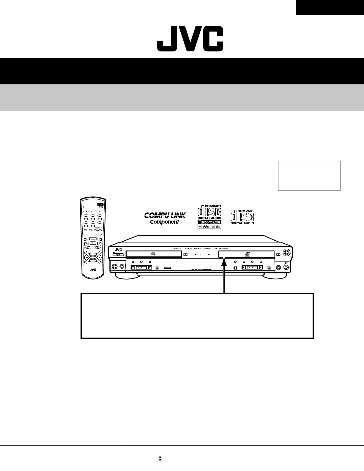
XL-R2010BK
SERVICE MANUAL
CD/CDR MULTIPLE COMPACT DISC RECORDER
XL-R2010BK
Area Suffix
J ------------- U.S.A.
C ---------- Canada
Contents
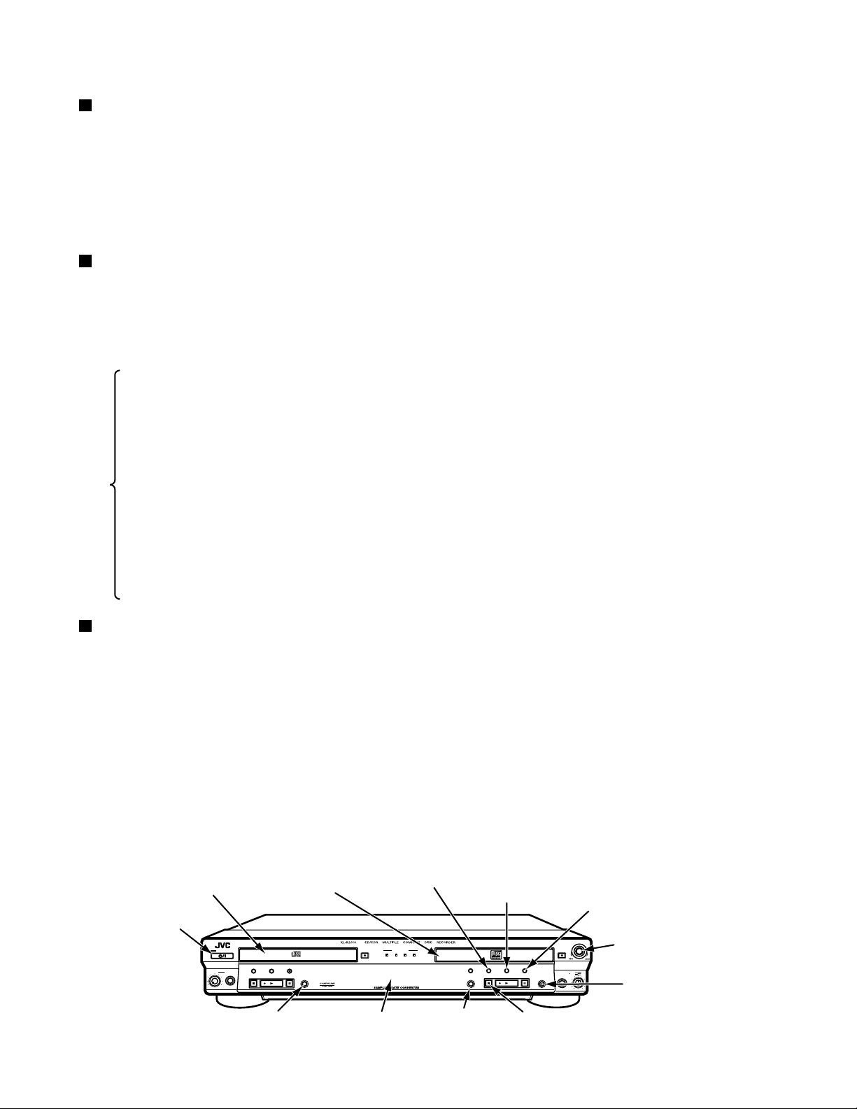
STANDBY/ON
CD EDIT FINALIZE DISPLA
CD REC
REC MUTING
R
S
PITCH
1 2
4 5
7 8
10
PLAY
MODE
REPEAT CD
REC
E
EC
OURC
0
RM-SXLR2010A
+
PITCH
SET
PITCH-
10
FADE SYNCHRO
+
REMOTE CONTROL
Y
3
6
9
CONTROL
CDR
REC MUTING
MULTI JOG/REC LEVEL
OPEN/CLOSEOPEN/CLOSE
+
-
CD
LINE
MIX BLANCE
MIC
REC/
LINE
MIC
MEN
U
STANDBY
STANDBY/ON
PLAY MODE CD EDIT
LEVEL
PHONES
L
E
NC
A
H
C
MAXMIN
STOP PLAY
CD REC
REC SOURCE
PAUSE
SELECTOR
REC SOURCE
DIGITAL CD LINE MIC
SYNCHRO
FINALIZE
CANCELSETMENU
PAUSE
PLAYSTOP
<ATTENTION of CD-R/RW mechanism unit>
Because the CD-R/RW mechanism unit is a unit exchange,
Moreover, the [Disassembly method],[Adjustment method],[Description of major ICs],
[Standard schematic diagram],[Printed circuit board],[Block diagram] of the CD-R/RW
mechanism unit is not described.
Safety precautions ------------------------ 1-2
Preventing static electricity ------------- 1-3
Importance admistering point
on the safety ------ 1-4
This service manual is printed on 100% recycled paper.
COPYRIGHT 2001 VICTOR COMPANY OF JAPAN, LTD.
Precautions for service ------------------ 1-5
Disassembly method -------------------- 1-6
Confirm method of operation ----------- 1-17
Description of major ICs ---------------- 1-20
No.A0013
Oct. 2001
Page 2
XL-R2010BK
1. This design of this product contains special hardware and many circuits and components specially for safety
purposes. For continued protection, no changes should be made to the original design unless authorized in
writing by the manufacturer. Replacement parts must be identical to those used in the original circuits. Services
should be performed by qualified personnel only.
2. Alterations of the design or circuitry of the product should not be made. Any design alterations of the product
should not be made. Any design alterations or additions will void the manufacturer`s warranty and will further
relieve the manufacture of responsibility for personal injury or property damage resulting therefrom.
3. Many electrical and mechanical parts in the products have special safety-related characteristics. These
characteristics are often not evident from visual inspection nor can the protection afforded by them necessarily
be obtained by using replacement components rated for higher voltage, wattage, etc. Replacement parts which
have these special safety characteristics are identified in the Parts List of Service Manual. Electrical
components having such features are identified by shading on the schematics and by ( ) on the Parts List in
the Service Manual. The use of a substitute replacement which does not have the same safety characteristics
as the recommended replacement parts shown in the Parts List of Service Manual may create shock, fire, or
other hazards.
4. The leads in the products are routed and dressed with ties, clamps, tubings, barriers and the like to be
separated from live parts, high temperature parts, moving parts and/or sharp edges for the prevention of
electric shock and fire hazard. When service is required, the original lead routing and dress should be
observed, and it should be confirmed that they have been returned to normal, after re-assembling.
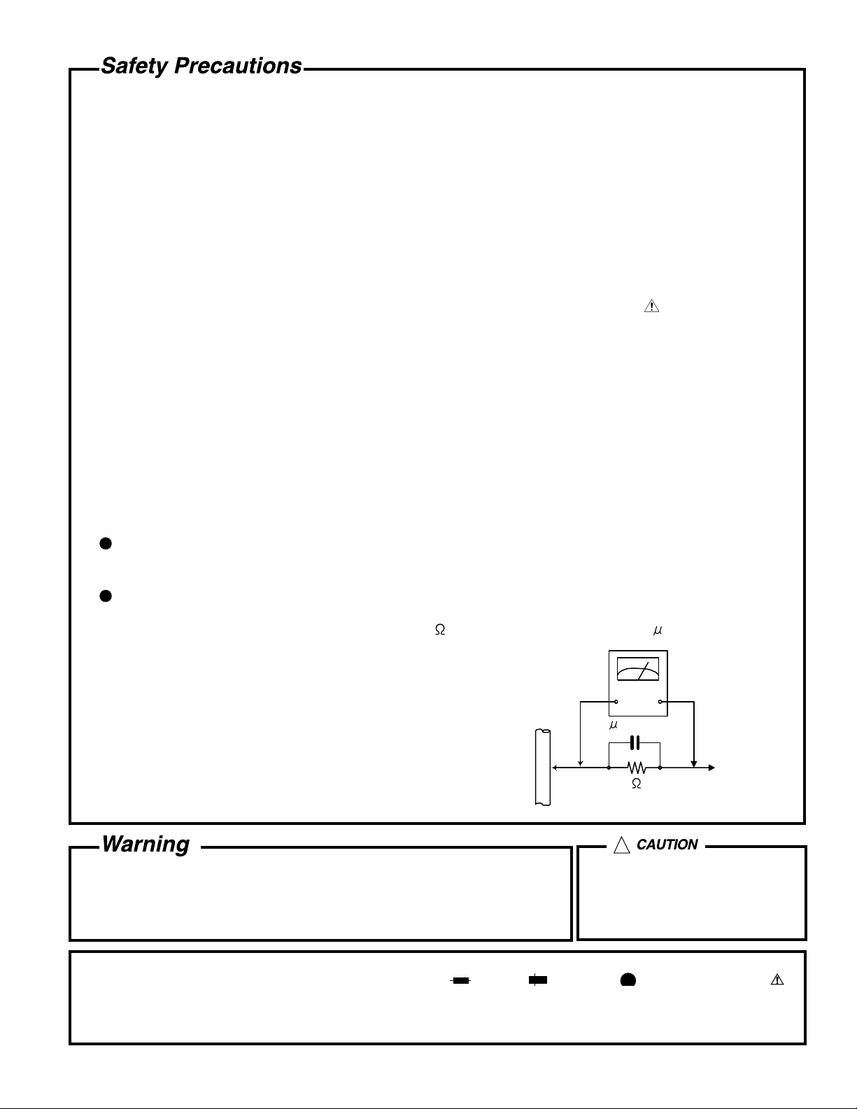
5. Leakage current check (Electrical shock hazard testing)
After re-assembling the product, always perform an isolation check on the exposed metal parts of the product
(antenna terminals, knobs, metal cabinet, screw heads, headphone jack, control shafts, etc.) to be sure the
product is safe to operate without danger of electrical shock.
Do not use a line isolation transformer during this check.
Plug the AC line cord directly into the AC outlet. Using a "Leakage Current Tester", measure the leakage
current from each exposed metal parts of the cabinet, particularly any exposed metal part having a return
path to the chassis, to a known good earth ground. Any leakage current must not exceed 0.5mA AC (r.m.s.).
Alternate check method
Plug the AC line cord directly into the AC outlet. Use an AC voltmeter having, 1,000 ohms per volt or more
sensitivity in the following manner. Connect a 1,500 10W resistor paralleled by a 0.15 F AC-type capacitor
between an exposed metal part and a known good earth ground.
Measure the AC voltage across the resistor with the AC
voltmeter.
Move the resistor connection to each exposed metal part,
particularly any exposed metal part having a return path to
the chassis, and measure the AC voltage across the resistor.
Now, reverse the plug in the AC outlet and repeat each
measurement. Voltage measured any must not exceed 0.75 V
AC (r.m.s.). This corresponds to 0.5 mA AC (r.m.s.).
0.15 F AC TYPE
1500 10W
Good earth ground
AC VOLTMETER
(Having 1000
ohms/volts,
or more sensitivity)
Place this
probe on
each exposed
metal part.
!
1. This equipment has been designed and manufactured to meet international safety standards.
2. It is the legal responsibility of the repairer to ensure that these safety standards are maintained.
3. Repairs must be made in accordance with the relevant safety standards.
4. It is essential that safety critical components are replaced by approved parts.
5. If mains voltage selector is provided, check setting for local voltage.
Burrs formed during molding may
be left over on some parts of the
chassis. Therefore, pay attention to
such burrs in the case of
preforming repair of this system.
1-2
In regard with component parts appearing on the silk-screen printed side (parts side) of the PWB diagrams, the
parts that are printed over with black such as the resistor ( ), diode ( ) and ICP ( ) or identified by the " "
mark nearby are critical for safety.
When replacing them, be sure to use the parts of the same type and rating as specified by the manufacturer.
(Except the J and C version)
Page 3
XL-R2010BK
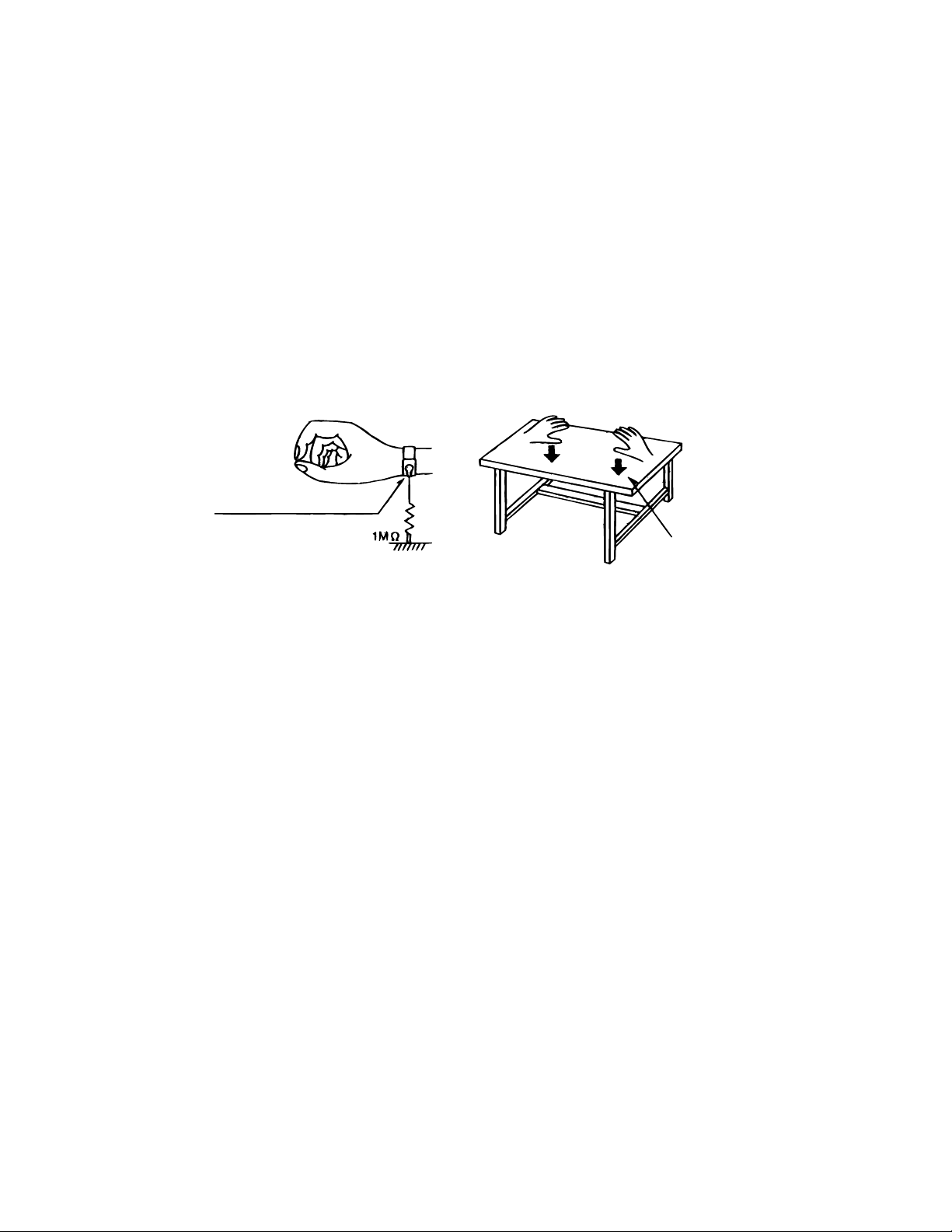
Preventing static electricity
Electrostatic discharge (ESD), which occurs when static electricity stored in the body, fabric, etc. is discharged,
can destroy the laser diode in the traverse unit (optical pickup). Take care to prevent this when performing repairs.
1. Grounding to prevent damage by static electricity
Static electricity in the work area can destroy the optical pickup (laser diode) in devices such as CD players.
Be careful to use proper grounding in the area where repairs are being performed.
1.1. Ground the workbench
1. Ground the workbench by laying conductive material (such as a conductive sheet) or an iron plate over
it before placing the traverse unit (optical pickup) on it.
1.2. Ground yourself
1. Use an anti-static wrist strap to release any static electricity built up in your body.
(caption)
Anti-static wrist strap
Conductive material
(conductive sheet) or iron plate
1.3. Handling the optical pickup
1. In order to maintain quality during transport and before installation, both sides of the laser diode on the
replacement optical pickup are shorted. After replacement, return the shorted parts to their original condition.
(Refer to the text.)
2. Do not use a tester to check the condition of the laser diode in the optical pickup. The tester's internal power
source can easily destroy the laser diode.
2. Handling the traverse unit (optical pickup)
1. Do not subject the traverse unit (optical pickup) to strong shocks, as it is a sensitive, complex unit.
2. Cut off the shorted part of the flexible cable after replacing the optical pickup. For specific
details, refer to the replacement procedure in the text. Remove the anti-static pin when replacing the traverse
unit. Be careful not to take too long a time when attaching it to the connector.
3. Handle the flexible cable carefully as it may break when subjected to strong force.
4. It is not possible to adjust the semi-fixed resistor that adjusts the laser power. Do not turn it
1-3
Page 4
XL-R2010BK
Importance Admistering point on the Safety
W913
B58
W903
CN501
B61
B43
B305
B42
B529
B309
B142
B235
CN723
B912
B914
B137
B233
R501
C501
B39
B310
B752
B758
B757
B756
B330
B329
B619
B618
W900
B27
B141
B131
B326
B327
B229
B230
B997
EP997
C917
B505
B504
B503
B502
B1
B707
B164
B302
B2
B3
C272
B162
B201
B401
B163
B501
CN841
C872
B102
B44
Q183
Q283
B101
C271
C171
Q181
J871
CN722
B303
Q841
B106
B6
Q842
B62
B5
B105
B202
C172
Q191
C874
C182
C282
B10
B12
B139
B11
Q182
Q282
B103
Q281
B304
B402
J354 J541
C543
B407
Q831
B8
B603
B602
B7
B601
Q832
B152
B9
B203
C1303
B405
C183
C283
C2303
C881
Q881
B24
B204
B161
B36
B306
B236
B17
B16
B107
Q821
R803
R802
B933
R801
Q822
B18
B15
B146
R821
B25
C1312
B63
C1301
Q1301
Q2301
B406
C2301
B506
B404
B113
B403
J353
J352
B130
B129
B408
B128
B412
B413
B111
B112
B110
R804
B20
C2302
B510
B411
B205
B323
B322
B206
B509
B410
B409
WC100
B945
C114
C804
C802
C214
C1302
T301
B507
B127
B207
C111
B208
C115
B209
B210
B307
B211
C215
B308
B417
B212
B913
C211
B116
B213
B214
B115
B21
B215
B158
C356
B22
B604
J351
C352
S531
EP998
B751
C381
B104
B234
C380
B48
B434
B331
CN616
B52
B40
C394
B41
B143
B156
B3612
B918
B138
C362
C361
B3603
B3604
B136
B620
X501
C367
X502
B328
B28
B29
B132
B31
B324
B325
W900
B114
B134
B133
B34
B30
CN615
W904
B33
B946
B612
B312
B216
K801
WC101
B32
C812
B528
B512
B416
B527
B607
B702
B608
B754
B610
B609
C840
B943
B511
B23
B3605
B3606
B418
B419
C830
R861
Q862
B701
B117
B753
Q541
B217
Q542
B159
C998
B998
B166
B135
K3601
K3600
B916
Q361
B915
B332
K3602
B38
B917
B3613
B3611
B126
C365
C366
B524
B37
B605
B55
B118
B301
R390
W902
W913
Q369
B169
B931
B926
B923
B508
B929
B928
B432
B615
B525
D812
B109
B526
B755
B932
B705
B613
B513
B108
B514
B919
B703
B920
B944
B934
B935
B936
B937
B611
C151
C1505
C251
Q861
B313
B939
B940
B941
B51
B942
B530
B150
B54
B160
C983
D956
C982
L957L958
C984
B144
B436
B35
B145
B49
B45
B46
B59
B47
B930
B435
B167
B14
C994
B153
B433
B155
B125
B157
B168
B925
B517
B50
CN505
B938
Q501
B56
C502
IC502
C2505
B57
WC102
B123
C975
C967
B119
C981
B905
B924
B521
C990
B909
B124
B147
B122
B320
R956
B224
C960
B422
B614
B121
C961
B222
C963
B120
CN721
C964
W901
C977
B53
L960
C985
C966
C987
L955
L953
C997
D971
EP951
C973
B140
B60
D970
Q965
C970
IC951
R972
B226
PC902
R975
Q967
R969
L951
R913
C919
PC901
R917
D960
C962
CP951
D972
C916
D973
R954
C980
B154
R952
C989
L959
L952
CP952
R973
D951
Q966
D952
D957
R974
D953
C965
W901
W902
W903
W904
D954
C979
HS901
IC901
R907
K901
R912
R906
C918
D907
R908
R918
D910
B906
R904
B947
D901
B907
D904
D905
B910
B948
C914
R910
R911
B911
R903
C913
D902
D903
C909
C908
T901
CN712 CN711
B999
C999
B165
EP999
B904
D913
C921
C922
B706
B64
B13
R914
T902
R905
R909
C903
B901
C907
R901
B148
C974
HS922
D974
Q922
C924
Q921
C923
D912
C920
D921
L901
C902
P901
Q980
R919
D980
B26
R980
R981
R982
R915
EP801
C906
FC904
B151
FC903
FC901FC902
F901
CN900
B149
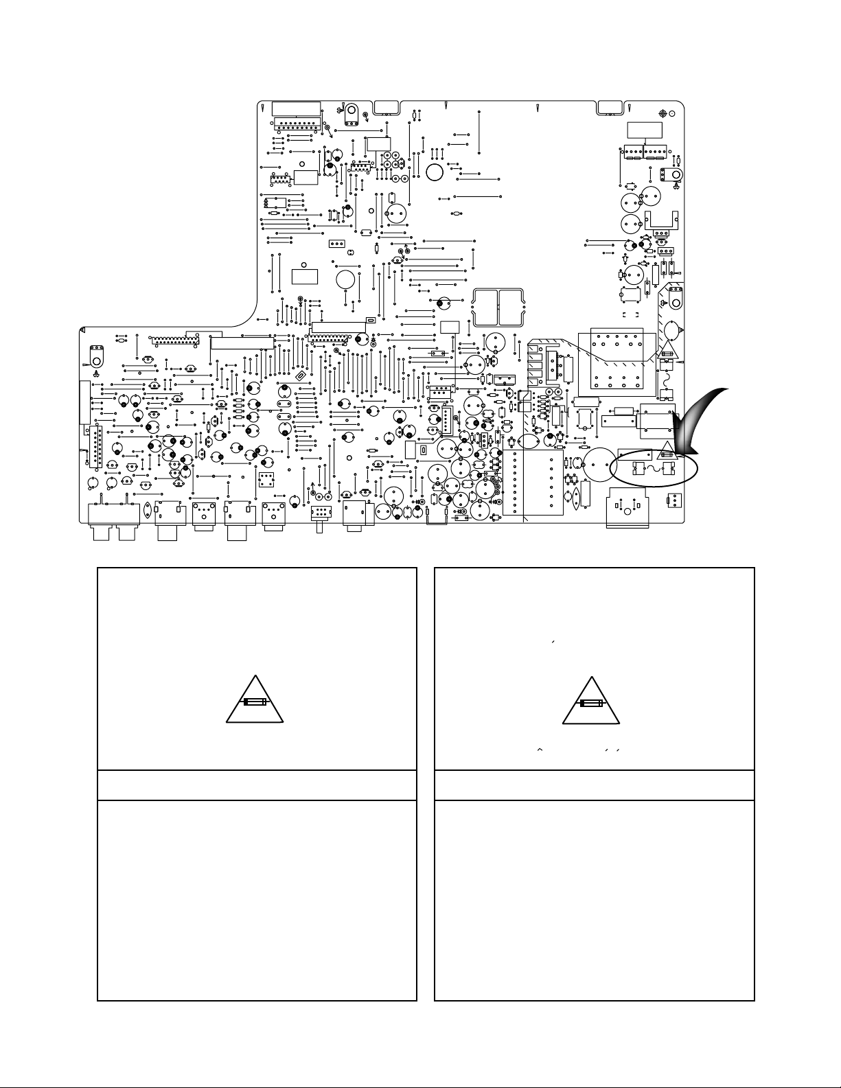
Full Fuse Replacement Marking
Marquage Pour Le Remplacement
Complet De Fusible
Graphic symbol mark
(This symbol means fast blow type fuse.)
should be read as follows ;
FUSE CAUTION
FOR CONTINUED PROTECTION AGAINST RISK
OF FIRE, REPLACE ONLY WITH SAME TYPE
AND RATING OF FUSES ;
Le symbole graphique (Ce symbole signifie
fusible de type a fusion rapide.)
doit etre interprete comme suit ;
PRECAUTIONS SUR LES FUSIBLES
POUR UNE PROTECTION CONTINUE CONTRE
DES RISQUES D'INCENDIE, REMPLACER
SEULEMENT PAR UN FUSIBLE DU MEME TYPE ;
F901 : 1.6 A / 125 V F901 : 1.6 A / 125 V
1-4
Page 5
Precautions for Service
Handling of Traverse Unit and Laser Pickup
1. Do not touch any peripheral element of the pickup or the actuator.
2. The traverse unit and the pickup are precision devices and therefore must not be subjected to
strong shock.
3. Do not use a tester to examine the laser diode. (The diode can easily be destroyed by the
internal power supply of the tester.)
4. To replace the traverse unit, pull out the metal short pin for protection from charging.
5. When replacing the pickup, after mounting a new pickup, remove the solder on the short land
which is provided at the center of the flexible wire to open the circuit.
6. Half-fixed resistors for laser power adjustment are adjusted in pairs at shipment to match the
characteristics of the optical block.
Do not change the setting of these half-fixed resistors for laser power adjustment.
Destruction of Traverse Unit and Laser Pickup by Static Electricity
Laser diodes are easily destroyed by static electricity charged on clothing
or the human body. Before repairing peripheral elements of the traverse
unit or pickup, be sure to take the following electrostatic protection:
XL-R2010BK
1. Wear an antistatic wrist wrap.
2. With a conductive sheet or a steel plate on the workbench on which
the traverse unit or the pick up is to be repaired, ground the sheet
or the plate.
3. After removing the flexible wire from the connector (CN601),
short-circuit the flexible wire by the metal clip.
4. Short-circuit the laser diode by soldering the land which is provided
at the center of the flexible wire for the pickup. After completing the repair, remove the solder
to open the circuit.
Please refer to [ Removing the mechanism board ] and [ Removing the pickup ] of the
Disassembly method < CD Mechanism assembly >.
Flexible wire
Shorting round
CN601 on
mechanism
board
<ATTENTION of CD-R/RW mechanism unit>
Because the CD-R/RW mechanism unit is a unit exchange,
the pick-up need not be detached alone.
Moreover, the [Disassembly method],[Adjustment method],
[Description of major ICs],[Standard schematic diagram],
[Printed circuit board],[Block diagram] of the CD-R/RW
mechanism unit is not described.
CD Mechanism assembly
1-5
Page 6
XL-R2010BK
Disassembly method
<Main body>
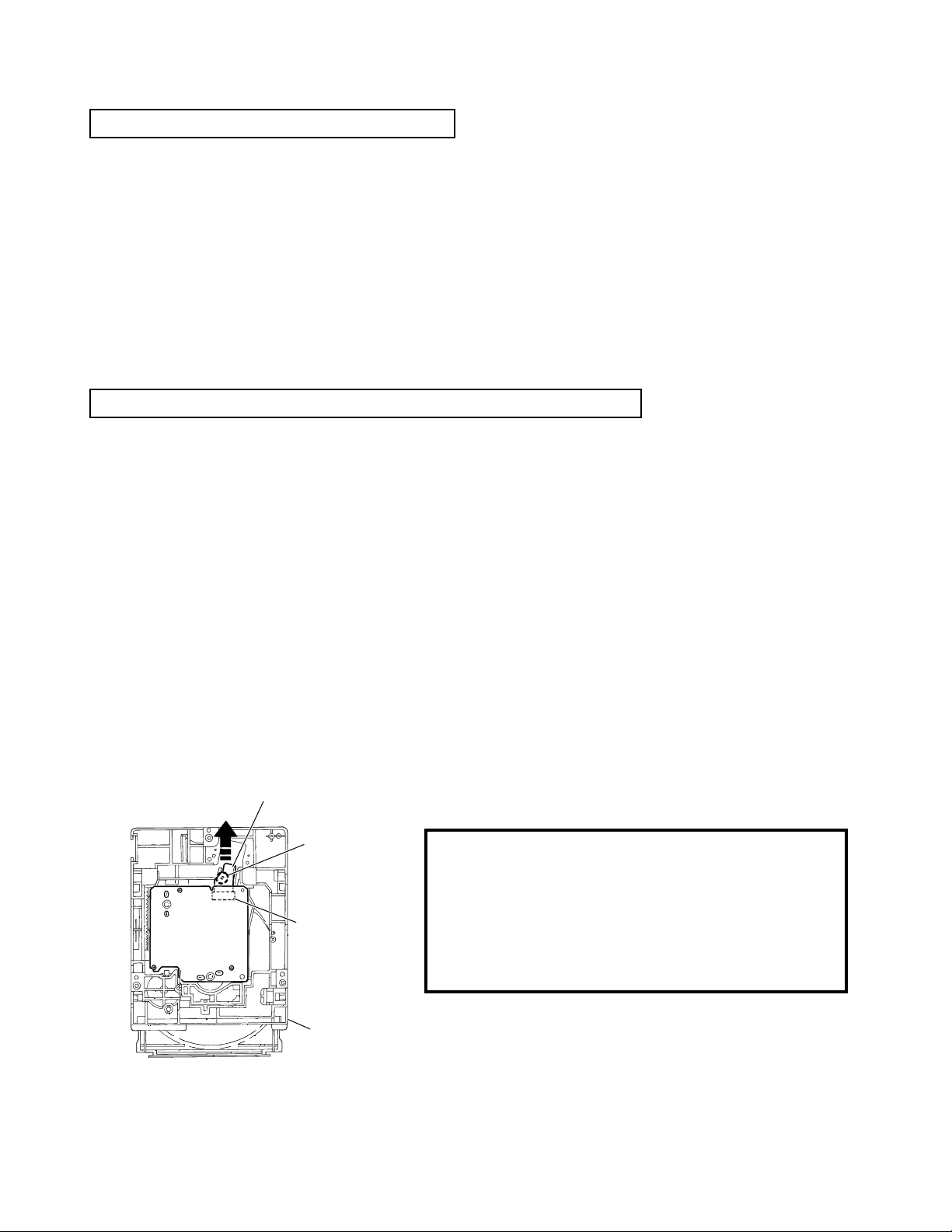
Removing the top cover (See Fig.1)
Remove the four screws A on both sides of the body.
1.
Remove the two screws B on the back of the body.
2.
Remove the top cover from behind in the direction of
3.
the arrow while pulling its sides outwards. Disengage
the three joints a with the front panel section.
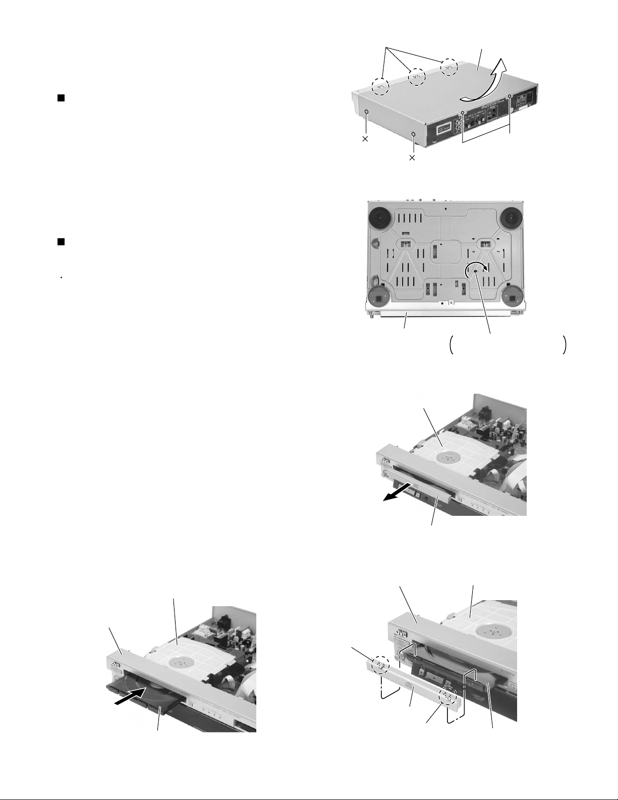
Removing the fitting of the CD
mechanism section (See Fig.2 to 5)
Prior to performing the following procedure, remove
the top cover.
Insert a Philips screwdriver into the hole of the
1.
chassis base on the bottom and turn it as shown in
the figure. The tray will move forward.
Pull out the tray manually.
2.
Joints a
A
2
A
2
Fig.1
Front panel assembly
Fig.2
Top cover
B
(Bottom)
Hole of the CD mechanism
section to pull out the tray
Release the joint b on each side of the fitting
3.
upward, then remove the fitting from the tray.
Push and return the tray.
4.
CD mechanism assembly
Front panel assembly
CD mechanism assembly
Front panel assembly
Joint b
Fitting
Fig.3
CD mechanism assembly
1-6
Tray
Fitting
Joint b
Tray
Fig.4Fig.5
Page 7
XL-R2010BK
Removing the fitting of the CD-R/RW
mechanism section (See Fig.6 to 9)
Prior to performing the following procedure, remove
the top cover.
Push the slide cam c until it stops through the slot on
1.
the left side of the CD-R/RW mechanism assembly.
Pull out the tray manually.
2.
Release the joint d on each side of the fitting
3.
upward, then remove the fitting from the tray.
Push and return the tray.
4.
Front panel assembly
Slide cam c
CD-R/RW mechanism
assembly
Slot
Slot of the CD-R/RW mechanism
section to pull out the tray
Fig.6
CD-R/RW mechanism assembly
Joint d
Fitting
Fitting
Joint d
Front panel assembly
Fig.7
CD-R/RW mechanism assembly
Tray
Fig.8
Tray
CD-R/RW mechanism assembly
Fig.9
1-7
Page 8
XL-R2010BK
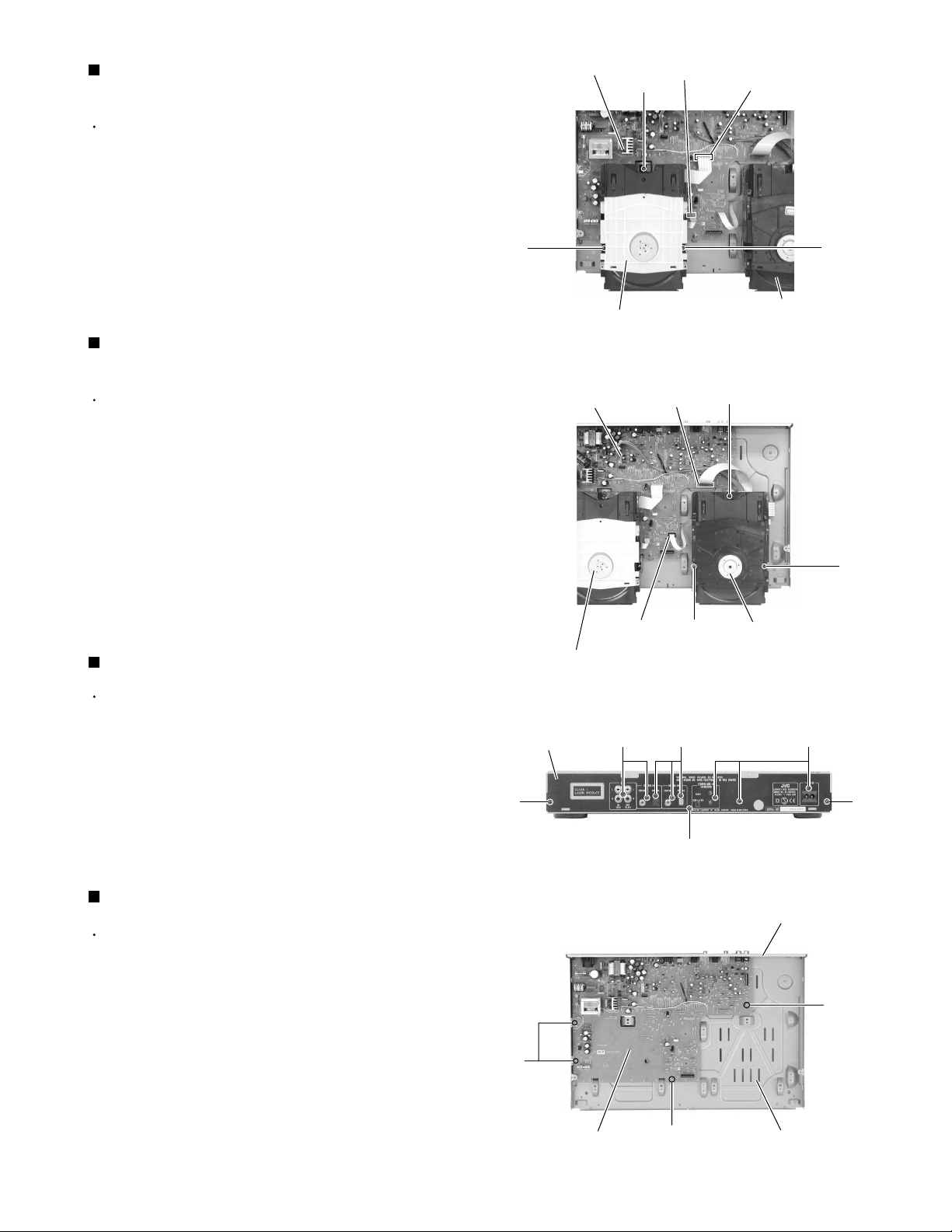
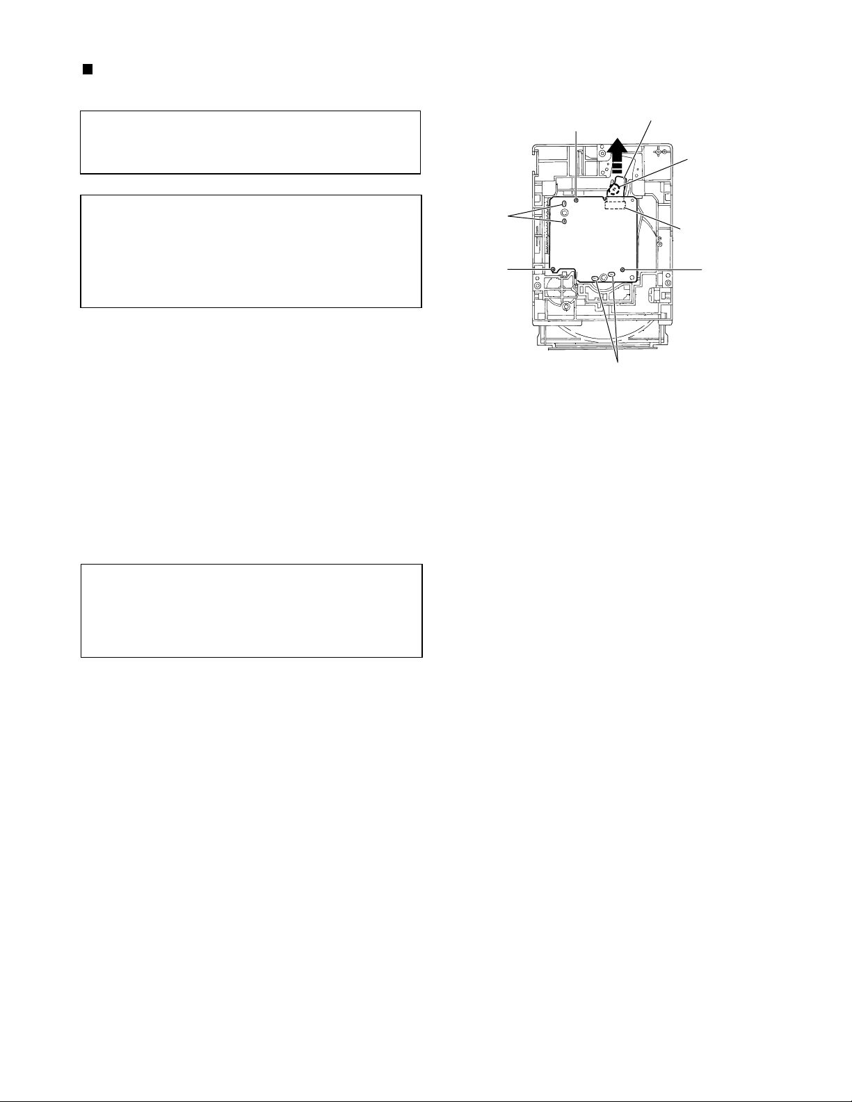
Removing the front panel assembly
(See Fig.10 to 14)
Prior to performing the following procedure, remove
the top cover and both fittings of the CD mechanism
section and the CD-R/RW mechanism section.
Disconnect the card wires from connector CN501,
1.
CN841 and the wires from CN711 and CN712 on the
main board from above.
Remove the screw C and the screw D attaching the
2.
headphone board and the mic board on the top of
the body.
Remove the four screws E attaching the right and
3.
left foot at the bottom.
Remove the two screws F and the screw G
4.
attaching the front panel assembly at the bottom.
Disengage the joint e on the bottom and the joints f
5.
on each side of the body to release the front panel
assembly from the chassis base using a slotted
screwdriver. Then remove the front panel assembly
toward the front.
CN712
CN711
C
Headphone board
Front panel assembly
Foot
E
Main board
Fig.10
(Bottom)
CN841
CN501
D
Mic board
Foot
E
C
Front panel assembly
Front panel assembly
F
Front panel assembly
Front panel assembly
Fig.11
(Bottom)
G
Fig.12
D
F
Joint e
1-8
Headphone board
Joint f
Joint f
Mic board
Fig.13Fig.14
CN801
Chassis base
Page 9
XL-R2010BK
Removing the CD mechanism assembly
(See Fig.15)
Prior to performing the following procedure, remove
the top cover and the fitting.
(Remove the front panel assembly is easy to work.)
Disconnect the card wire from connector CN615 and
1.
CN616 on the main board from above.
Remove the three screws H attaching the CD
2.
mechanism assembly.
Removing the CD-R/RW mechanism
assembly (See Fig.16)
Prior to performing the following procedure, remove
the top cover and the fitting.
(Remove the front panel assembly is easy to work)
Disconnect the wire from connector CN721 and the
1.
card wires from CN722 and CN723 on the main
board from above.
Main board
H
H
CD mechanism assembly
CN721
Main board
CN722
CN616
Fig.15
CN615
H
CD-R/RW mechanism
assembly
I
Remove the three screws I attaching the CD-R/RW
2.
mechanism assembly.
Removing the rear panel (See Fig.17)
Prior to performing the following procedure, remove
the top cover.
Remove the three screws J and the eight screws K
1.
on the back of the body.
Removing the main board (See Fig.18)
Prior to performing the following procedure, remove
the top cover, the front panel assembly, the CD
mechanism assembly, the CD-R/RW mechanism
assembly and the rear panel.
Remove the four screws L attaching the main board.1.
CN723
CD mechanism assembly
Rear panel
K
J
I
Fig.16
K
J
Fig.17
I
CD-R/RW mechanism
assembly
K
J
Rear panel
L
L
Main board
L
Fig.18
Chassis base
1-9
Page 10
XL-R2010BK
<Front panel assembly>
Removing the headphone board / power
switch board (See Fig.19 to 21)
Pull out the volume knob on the front panel
1.
assembly.
Remove the two screws M attaching the headphone
2.
board bracket and the three screws N attaching the
power switch board. Remove the headphone board
and the power switch board at the same time.
Pull out the stopper attaching the headphone board
3.
bracket in the direction of the arrow.
Front panel assembly
Volume knob
Fig.19
N
Power switch board
Headphone board
Power switch board
M
Headphone board bracket
M
Fig.20
Headphone board
1-10
Stopper
Headphone board bracket
Fig.21
Page 11
XL-R2010BK
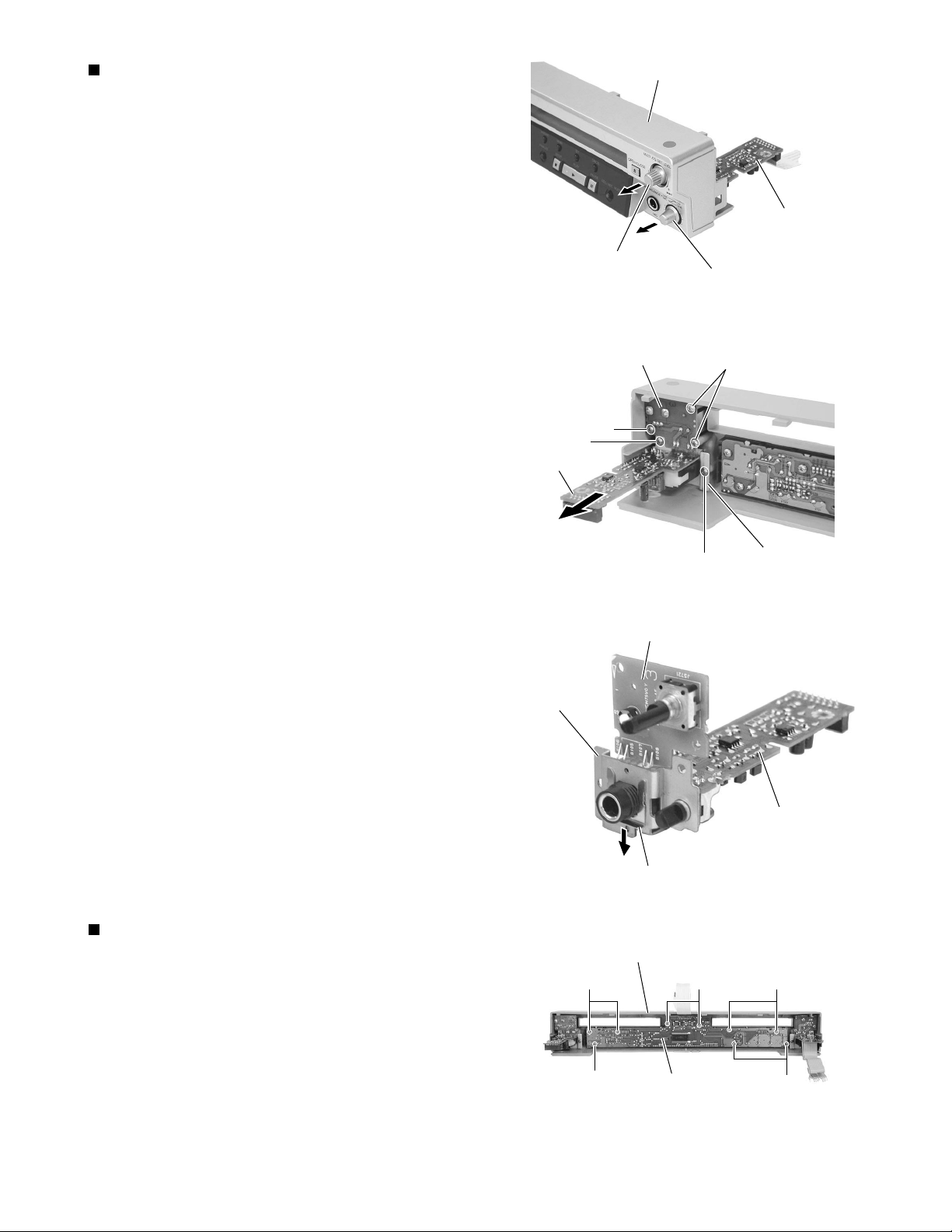
Removing the mic board / jog dial board
(See Fig.22 to 24)
Pull out the jog dial knob and the mix balance knob
1.
on the front panel assembly.
Remove the two screws O attaching the mic board
2.
bracket and the three screws P attaching the jog dial
board. Remove the mic board and the jog dial board
at the same time.
Pull out the stopper attaching the mic board bracket
3.
in the direction of the arrow.
Jog dial knob
Mic board
Front panel assembly
Jog dial board
P
O
Mic board
Mix balance knob
Fig.22
P
Removing the front board (See Fig.25)
Remove the nine screws Q on the back of the front
1.
panel assembly.
Mic board bracket
Front panel assembly
Q
Fig.23
Jog dial board
Stopper
Fig.24
Q
O
Mic board bracket
Mic board
Q
Q
Front board
Fig.25
Q
1-11
Page 12
XL-R2010BK
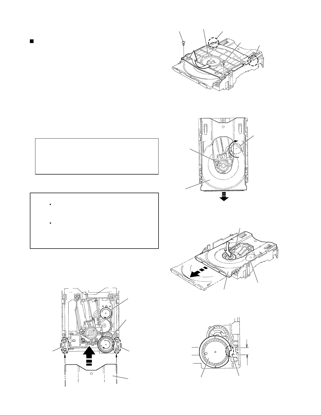
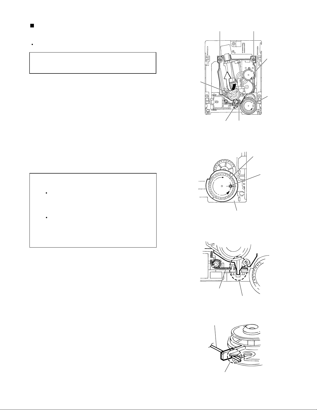
<CD Mechanism assembly>
Clamper base assembly
A
Hook a
Removing the clamper base assembly and
tray (See Figs. 1 to 5)
1. Remove the two screws A attaching the clamper
base assembly from the top of the CD mechanism
assembly.
2. Move the clamper base assembly diagonally
upwards as indicated by the arrow to release it from
the two hooks a.
3. Turn the idle gear in the arrow-marked direction
from the upper side of the CD mechanism
assembly. Accordingly, the traverse mechanism
assembly moves downwards.
Note: When drawing out the tray, shift down the
traverse mechanism assembly to the
position where the tray does not contact the
turn table assembly of the traverse
mechanism assembly.
4. Draw out the tray frontwards for removing it.
Traverse
mechanism
assembly
Tray
Fig. 1
A
Hook a
Idle gear
Note: When reinstalling the tray:
Turn the idle gear so that the part b of the
tray gear is positioned in the part c shown in
Fig. 4. (Eject position)
Engage the right and left hooks d and e of
the tray with the right and left grooves of the
loading mechanism assembly respectively
for retaining the tray.
Idle gear
Tray gear
Hook d
Hook e
Fig. 2
Traverse mechanism assembly
Idle gear
Tray
Fig. 3
Part c
1-12
Tray
Tray gear
Part b
Fig. 4Fig. 5
Page 13
XL-R2010BK
Removing the traverse mechanism assembly
(See Figs. 6 to 9)
Remove the clamper base assembly and tray.
Reference: The traverse mechanism assembly can
be removed without removal of the
mechanism board.
1. If the traverse mechanism assembly is lowered and it is
located out of the PLAY position, turn the idle gear in the
arrow-marked direction so that the hole in the part f of the
tray gear meets the hole on the loading base assembly.
(Set the traverse mechanism assembly at the PLAY
position.)
2. Remove the three screws B attaching the traverse
mechanism assembly and then remove the traverse
mechanism assembly upwards from the front side.
3. At the same time, remove the spring from the groove of the
CH. base assembly in the part g of the traverse
mechanism assembly.
Note: When reinstalling the traverse mechanism
assembly:
Check to see if the spring is properly
engaged with groove of the CH. base
assembly in the part g of the traverse
mechanism assembly.
After making sure that the three insulators of
the traverse mechanism assembly are
properly set on the bosses of the loading
base assembly's guide, fasten them with the
screws.
Traverse
mechanism
assembly
B
Part g
Fig. 6
Loading base assembly
Fig. 7
B
B
Tray gear
Idle gear
Tray gear
Part f
Spring
Part g
Fig. 8
Spring
Groove of CH. base assembly
Fig. 9
1-13
Page 14
XL-R2010BK
Removing the mechanism board
Reference:The mechanism board can be removed
(See Fig 10)
without removal of the traverse
mechanism assembly.
C
Flexible wire
Shorting round
Note: Before disconnecting the flexible wire coming
from the pickup from the connector, be sure to
solder its shorting round.
If the flexible wire is connected without
soldering, it may cause breakdown of the
pickup.
1. Solder the shorting round of the flexible wire
connected with the mechanism board from the back
of the mechanism assembly.
2. Disconnect the flexible wire from the connector
CN601 on the mechanism board.
3. Remove the three screws C attaching the
mechanism board.
4. Unsolder the two points of the part h and two point
of the part i of the mechanism board. Then, remove
the mechanism board upwards.
Note: When reinstalling the mechanism board,
connect the flexible wire coming from the
pickup to the connector first and then remove
the solder from the shorting round of the
flexible wire.
Soldered
part h
C
CN601 on
mechanism
board
C
Soldered part i
Fig. 10
1-14
Page 15
XL-R2010BK
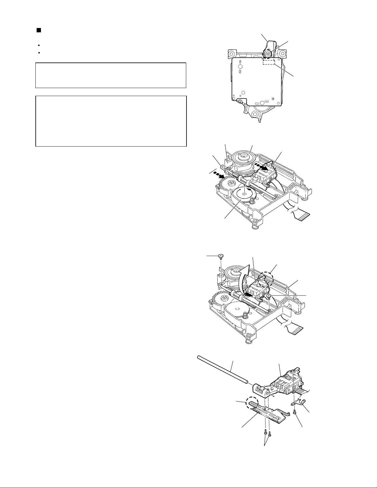
Removing the pickup (See Figs. 11 to 14)
Remove the clamper base assembly and tray.
Remove the traverse mechanism assembly.
Reference: The pickup can be removed without
removal of the mechanism board.
Note: Before disconnecting the flexible wire coming
from the pickup from the connector, be sure to
solder its shorting round.
If the flexible wire is connected without
soldering, it may cause breakdown of the
pickup.
1. Solder the shorting round of the flexible wire
connected with the mechanism board from the back
of the traverse mechanism assembly.
2. Disconnect the flexible wire from the connector
CN601 on the mechanism board.
3. Turn the idle gear in the arrow-marked direction from
the top of the traverse mechanism assembly so that
the pickup assembly is shifted to the reverse side of
the turn table assembly.
Move the pickup assembly until the part j of the rack
plate in the lower part of the pickup assembly comes
out of the CH. base assembly.
4. Remove the two screws D attaching the shaft of the
pickup assembly. Next, disengage the part k from
the CH. base assembly and then remove the pickup
assembly together with the shaft.
5. Pull the shaft out of the pickup.
Part j of
rack plate
Idle gear
D
CH. base
assembly
Pickup assembly
Flexible wire
Shorting round
CN601 on
mechanism
board
Fig. 11
Turn table assembly
Pickup assembly
Fig. 12
Par t k
CH. base
assembly
D
6. Remove the two screws E attaching the rack plate
from the pickup.
7. Remove the screw F attaching the P.S. spring from
the pickup.
Shaft
Par t j
Rack plate
Fig. 13
Pickup
P.S. spring
F
E
Fig. 14
1-15
Page 16
XL-R2010BK
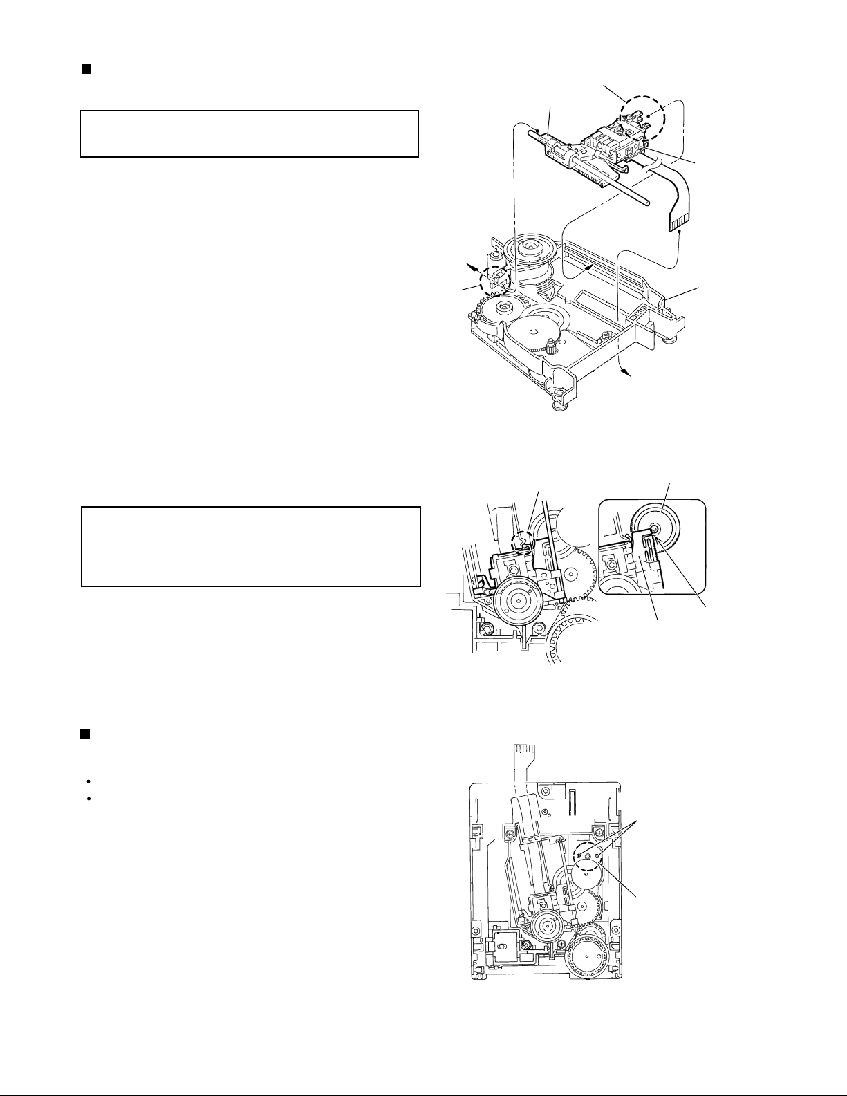
Reinstalling the pickup assembly
(See Figs. 15 and 16)
Reference: Refer to the explanation of "Removing
the Pickup" on the preceding page.
1. Fit the P.S. spring and rack plate to the pickup.
2. Insert the shaft into the pickup.
3. Engage the part k of the pickup assembly with the
CH. base assembly first, and set the part j of the
rack plate in the opening I next. Then, reinstall the
pickup assembly while shifting it to the turn table
side (inward) so that the part m of the rack plate is
positioned as shown in Fig. 16.
4. Move the pickup assembly to the center position
and fasten the shaft with the two screws D. (Make
sure that the part n of the rack plate is correctly
engaged with the middle gear.)
5. After passing the flexible wire coming from the
pickup through the opening of the CH. base
assembly, connect it to the connector CN601.
Part I
Part j
Part m
Part k
Pickup
assembly
CH. base
assembly
Fig. 15
Middle gear
Note: When reinstalling the pickup assembly,
remove the solder from the shorting round
after connecting the flexible wire coming from
the pick to the connector CN601.
Removing the feed motor assembly
(See Fig. 17)
Remove the clamper base assembly and tray.
Remove the mechanism board.
Remove the two screws G attaching the feed motor
assembly from the top of the mechanism assembly.
Rack plate
Part n
Fig. 16
G
Feed motor assembly
1-16
Fig. 17
Page 17
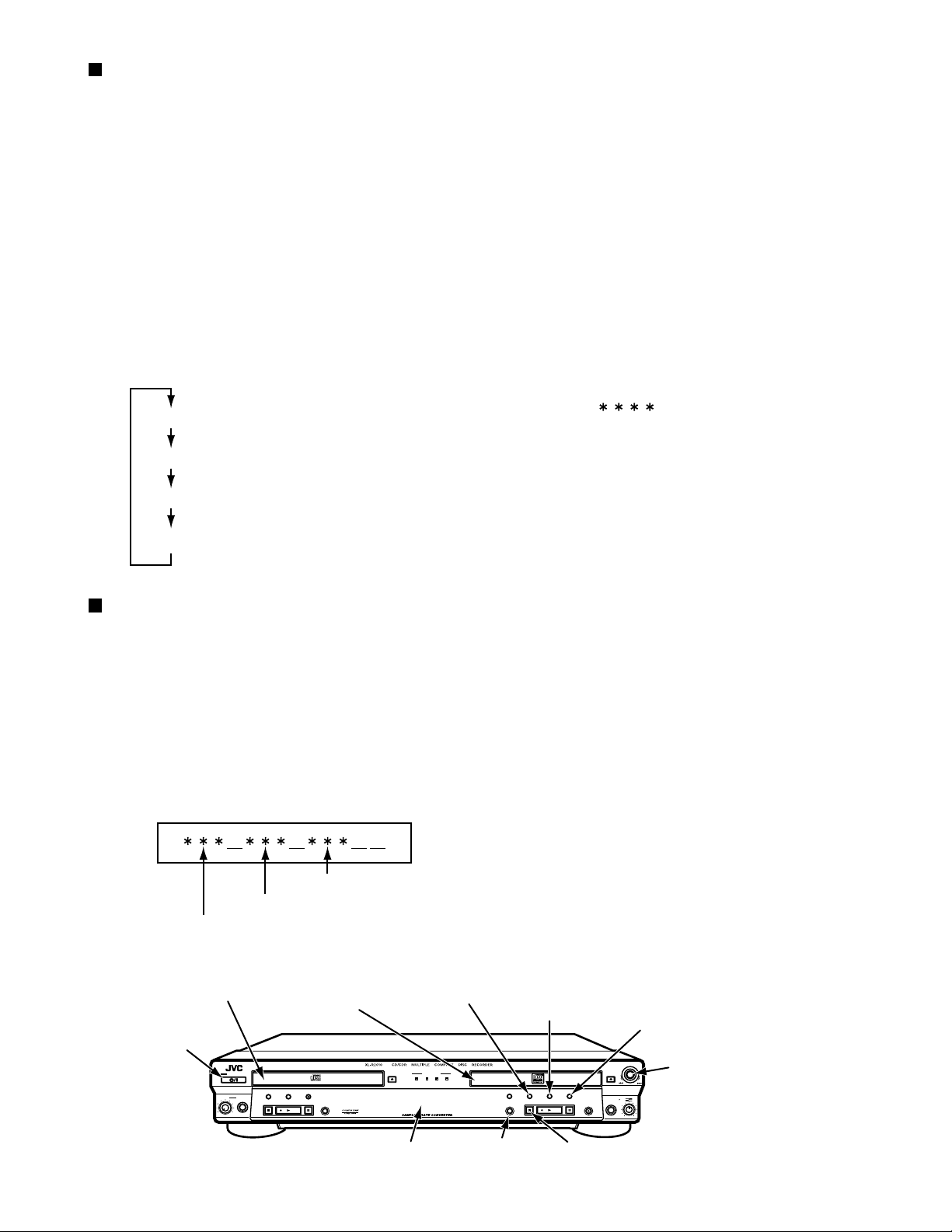
Confirm method of operation
Check mode (All lighting FL display)
<Setting method>
"STANDBY/ON" key is pushed while pushing "REC/REC MUTING" key by the stand-by state.
<Release method>
The key to "STANDBY/ON" is pushed.
(Please set the above-mentioned again to light all FL displays again after the check mode is made clear
after pulling out the power cord once.)
All release of set content
All content of the item in the following set is returned to initial state. (State of factory shipment)
<Setting method>
"STANDBY/ON" key is pushed while pushing "REC SOURCE SELECTOR" key by the stand-by state.
[Set items]
The program of the program play is deleted.
The content of the registration of the listening editing and the program editing is deleted.
The repeat setting is turned off.
Release of disc lock
A current unit is set to the CD mechanism unit side.
The play mode of CD mechanism unit is made a normal mode.
The pitch control setting is turned off.
The selection of the recording source is made DIGITAL of CD.
DUB-SPEED setting is made HIGH.
AUTO TRACK setting is turned ON.
TRACK SPACE setting is turned ON.
CONVERTER setting is turned ON.
D-IN SYNCHRO setting is START
FINALIZE setting is OFF
XL-R2010BK
Service menu
The running operation and the version of the firmware can be confirmed by the undermentioned method.
(Does not use excluding "SYSTEM_AGING" and "READ_VERSION" by the item displayed in the service menu.)
<Setting method of service menu>
1."STANDBY/ON" key is pushed while pushing "FINALIZE" key by the stand-by state.
2.When the blinking display of the disc distinction ends, "MENU" key is pushed.
The menu display changes if "MULTI JOG" knob of the main body is turned.
3.The execution of the each item is completed or either "CANCEL"key, "CD-RW STOP"key or "MENU"key
is pushed when going out of the menu mode.
<Release method>
If "STANDBY/ON" key is pushed, and the power supply is turned off once, becomes a normal menu.
MENU key
(Menu mode ON)
REC SOURCE
DIGITAL CD LINE MIC
FL Display
SET key
(Execution)
SYNCHRO
FINALIZE
FINALIZE key
(Service menu)
(Release of menu mode)
MULTI JOG/REC LEVEL
OPEN/CLOSEOPEN/CLOSE
+
REC MUTING
-
CD
LINE
MIX
LINE
MIC
REC/
MIC
CANCELSETMENU
PAUSE
PLAYSTOP
STOP key
(Release of menu mode)
CANCEL key
MULTI JOG knob
(Service menu display switch)
REC/REC MUTING key
(All lighting FL display)
CD Mechanism unit
STANDBY/ON key
REC SOURCE SELECTOR key
(All release of set content)
CD-R/RW
Mechanism unit
STANDBY
STANDBY/ON
PLAY MODE CD EDIT
STOP PLAY PAUSE
CD REC
REC SOURCE
SELECTOR
LEVEL
PHONES
MAXMIN
1-17
Page 18
XL-R2010BK
Running operation
When this mode is executed, the operation of the recording and the playback is repeated.
Please use to confirm operation.
It is necessary to put the recorded disc or CD-DA in tray of CD mechanism unit beforehand to
execute this item, and put CD-RW of the blank disc in CD-R/RW mechanism unit.
<Setting method of running operation>
1."Service menu" is made to be displayed on the FL display referring to the previous page.
2."SYSTEM_AGING" is made to turn "MULTI JOG" knob, and to be displayed on the FL display.
3.The undermentioned operation starts when "SET" key is pushed.
The undermentioned control becomes possible according to the content of the disc turned on to tray
of CD mechanism unit.
* The time required of operation of running once
* Movement frequency of pick-up
1 Disc recording
Finalize
F L display becomes " ", and the frequency to
which the running operation is done is displayed by the
figure when "STOP" key is pushed to the running working
or interrupted because of the error etc.
CD-RW is playback to the last minute.
DISC ERASE for CD-RW.
Display of version number
When this item is executed, version number "system controller", "CD-R/RW mechanism unit", and
"CD mechanism unit" respectively is displayed in FL display for five seconds.
When five seconds pass, this mode is automatically made clear.
<Setting method of display of version number>
1."Service menu" is made to be displayed on the FL display referring to the previous page.
2."READ_VERSION" is made to turn "MULTI JOG" knob, and to be displayed on the FL display.
3.The undermentioned operation starts when "SET" key is pushed.
FL Display
1-18
System controller version number
CD Drive unit
STANDBY/ON key
CD mechanism unit version number
CD-R/RW mechanism unit version number
MENU key
CD-R/RW Drive unit
STANDBY
STANDBY/ON
PLAY MODE CD EDIT
STOP PLAY PAUSE
CD REC
REC SOURCE
SELECTOR
LEVEL
PHONES
MAXMIN
(Menu mode ON)
REC SOURCE
DIGITAL CD LINE MIC
FL Display
FINALIZE key
(Service menu)
SET key
(Execution)
SYNCHRO
FINALIZE
It is displayed instead of version
number when failing in reading
version number, "000".
(Release of menu mode)
MULTI JOG/REC LEVEL
OPEN/CLOSEOPEN/CLOSE
+
REC MUTING
-
CD
LINE
MIX
LINE
MIC
REC/
MIC
CANCELSETMENU
PLAYSTOP
PAUSE
STOP key
(Release of menu mode)
CANCEL key
MULTI JOG knob
(Service menu display switch)
Page 19

Extension cord for diagnosis of CD mechanism unit
It is an extension cord to operate with the CD mechanism unit removed from the main body.
Each connector is connected by the extension cord and used as shown in the figure below.
Parts No. QUQ110-1936AJ
CN651
XL-R2010BK
CN606
CD Servo control board
Parts No. QUQ110-0838AJ
CN615
CN616
Main board
1-19
Page 20

XL-R2010BK
Dscription of major ICs
AN22000A-W(IC601):RF & SERVO AMP
1. Pin layout
PD
1
LD
2
VCC
3
RFN
RFIN
ARF
CEA
BDO
GND
4
5
6
7
8
9
10
11
12
13
14
15
16
RFOUT
CAGC
3TOUT
CBDO
COFTR
OFTR
RFDET
2. Pin function
Pin
Symbol Description
No.
1
PD
2
LD
3
VCC
4
RFN
5
RF OUT
6
RF IN
7
C.AGC
8
ARF
9
CEA
10
3TOUT
11
CBDO
12
BDO
13
COFTR
14
OFTR
15
RFDET
A
32
C
31
B
30
D
29
PDF
28
PDE
27
TBAL
26
FBAL
25
GCTRL
24
FEOUT
23
FEN
22
TEN
21
TEOUT
20
TEBPF
19
VDET
18
VREF
17
APC Amp. Input terminal
APC Amp.Output terminal
Power supply terminal
RF addition Amp.Reversing input terminal
RF addition Amp.Output terminal
AGC input terminal
Terminal of connection of capacity of AGC loop
filter.
AGC output terminal
Capacity connection terminal for HPF-Amp.
3TENV output terminal
Capacity connection terminal for RF shade side
envelope detection
BDO output terminal
Capacity connection terminal for RF discernment
side envelope detection
OFTR output terminal
RFDET output terminal
Pin
Symbol Description
No.
16
17
18
19
20
21
22
23
24
25
26
27
28
29
30
31
32
GND
VREF
VDET
TEBPF
TEOUT
TEN
FEN
FEOUT
GCTRL
FBAL
TBAL
PDE
PDF
D
B
C
A
Connect to ground
VREF output terminal
VDET output terminal
VDET input terminal
TE Amp. output terminal
TE Amp. reversing input terminal
FE Amp. reversing input terminal
FE Amp. output terminal
Terminal GCTL & APC
FBAL control terminal
TBAL control terminal
Tracking signal input terminal 1
Tracking signal input terminal 2
Focus signal input terminal 4
Focus signal input terminal 2
Focus signal input terminal 3
Focus signal input terminal 1
BU4066BCF-X(IC821,IC831,IC841,IC861):Source selector
1.Pin layout & block diagram 2.Truth table
1-20
I/O1
O/I1
O/I2
I/O2
C2
C3
Vss
1
2
3
4
5
6
7
14
13
12
11
10
9
8
Vdd
C1
C4
I/O4
O/I4
O/I3
I/O3
Control
H
L
Switch
ON
OFF
Page 21

LA6541-X (IC801) : Focus & Spindle & Feed & Tracking BTL driver
1. Pin layout & Block diagram
Vcc Vref Vin4 Vg4 Vo8 Vo7
24 23
22
21
20
19
11k
ohm
Vcc
Gnd
Vo6 Vo5 Vg3 Vin3 Cd Res
18
17 16
XL-R2010BK
15
14
11k
ohm
13
- +
- +
Level
shift
Level
shift
B T L
driver
B T L
driver
B T L
driver
B T L
driver
Level
shift
Level
shift
11k
ohm
1
Vcc Mute Vin1 Vg1 Vo1 Vo2 Vo3 Vo4 Vg2 Vin2 Reg
2
3456
Gnd
7 8 9101112
2. Pin function
Pin No. Symbol Description
1
2
3
4
5
6
7
8
9
10
11
12
13
14
15
16
17
18
19
20
21
22
23
24
Vcc
Mute
Vin1
Vg1
Vo1
Vo2
Vo3
Vo4
Vg2
Vin2
Reg Out
Reg In
Res
Cd
Vin3
Vg3
Vo5
Vo6
Vo7
Vo8
Vg4
Vin4
Vref
Vcc
Power supply (Shorted to pin 24)
All BTL amplifier outputs ON/OFF
BTL AMP 1 input pin
BTL AMP 1 input pin (For gain adjustment)
BTL AMP 1 input pin (Non inverting side)
BTL AMP 1 input pin (Inverting side)
BTL AMP 2 input pin (Inverting side)
BTL AMP 2 input pin (Non inverting side)
BTL AMP 2 input pin (For gain adjustment)
BTL AMP 2 input pin
External transistor collector (PNP) connection. 5V power supply output
External transistor (PNP) base connection
Reset output
Reset output delay time setting (Capacitor connected externally)
BTL AMP 3 input pin
BTL AMP 3 input pin (For gain adjustment)
BTL AMP 3 output pin (Non inverting side)
BTL AMP 3 output pin (Inverting side)
BTL AMP 4 output pin (Inverting side)
BTL AMP 4 output pin (Non inverting side)
BTL AMP 4 output pin (For gain adjustment)
BTL AMP 4 output pin
Level shift circuit's reference voltage application
Power supply (Shorted to pin 1)
11k
ohm
out
RESET
Regulator
Reg
In
1-21
Page 22

XL-R2010BK
M66004FP-X(IC721):FL Driver
1.Block diagram
FLCS
14
FLCLKK
15
16
FLDAT
13
RESET
Cereal
receive
circuit
Vcc Vcc2
19
60
Display code
register
(8bit 16)
control circuit
Code/Command
Display
control
register
RAM write
code select
CGROM
(35bit 160)
DecoderDecoder
CGRAM
(35bit 16)
Segment output circuit
Output port
(2bit)
23
P36
31
P28
P27
33
59
P01
P1
17
P0
18
XIN
21
XOUT
20
2.Pin function
Pin.No.
1~12
13
14
15
16
17
18
19
20
21
22
23~31
32
33~59
60
61~64
Clock
generation
circuit
12G~1G
FLCLK
FLDATA
P36~P28
P27~P01
16G~13G
Symbol
SRST
FLCS
P1
P0
VCC1
XOUT
XIN
VSS
VP
VCC2
Display
controller
22 32
Vss
I/O
FL grid control signal output.
O
Reset signal input
I
Chip select signal input.
I
Shift clock signal input.
I
Serial data input.
I
Output port (static operation)
O
Output port (static operation)
O
Power supply for internal logic.
-
Clock signal output.
O
Clock signal input.
I
Connect to ground.
-
FL Segment control signal output.
O
Power supply.
-
FL Segment control signal output.
O
Power supply for grid output and segment output.
-
FL grid control signal output.
O
Description
Grid
output
circuit
Vp
12G
1
12
1G
16G
61
64
13G
1-22
Page 23

MN662790RSC(IC651):Digital servo & processor
1.Pin layout
60 41
61
40
XL-R2010BK
80
21
1 20
2.Pin function
Pin No. Symbol I/O
1
2
3
4
5
6
7
8
9
10
11
12
13
14
15
16
17
18
19
20
21
22
23
24
25
26
27
28
29
30
31
32
33
34
35
36
37
38
39
40
BCLK
LRCK
SRDATA
DVDD1
DVSS1
TX
MCLK
M DATA
MLD
SENSE
FLOCK
TLOCK
BLKCK
SQCK
SUBQ
DMUTE
S TAT
LSI_RST
SMCK
CSEL
TEST2
TVD
PC
ECM
ECS
VDETMON
TRD
FOD
VREF
FBAL
TBAL
FE
TE
RFENV
TEST3
OFT
TRCRS
RFDET
BDO
LDON
O
O
O
-
-
O
I
I
I
-
-
-
O
I
O
I
O
I
O
I
-
O
O
O
O
O
O
O
I
I
I
I
I
I
I
I
-
MN662790RSC (1/2)
Description
Bit clock output for SRDATA
Identifying signal output of L,R
Serial data output
Power supply for digital circuit
Connect to ground for digital circuit
Digital audio interface output signal
Micom command clock signal input
Micom command data signal input
Micom command load signal input L:load
Non connect
Non connect
Non connect
Sub code block clock signal
Export clock signal input for sub code Q resister
Sub code Q data output
Muting input H:muting
Status signal output
Reset signal input L:reset
Clock signal output MSEL is H : 8.4672 MHz MSEL is L : 4.2336 MHz
Oscillation frequency specification terminal H:33.8688 MHz L:16.9344 MHz
TEST2 terminal usually : open
Traverse drive output
Non connect
Spindle motor drive signal output (Compulsion mode output)
Spindle motor drive signal output (Servo error signal output)
Non connect
Tracking drive signal output
Focus drive signal output
Reference voltage for DA output section
Focus balance adjust signal output
Tracking balance adjust signal output
Focus error signal input (analog input)
Tracking error signal input (analog input)
RF Envelope signal input (analog input)
TEST3 Terminal usually : Fixation L
Off track signal input H : off track
Track cross signal input (analog input)
RF detection signal input L : detection
Dropout signal input H : dropout
Non connect
(Command execution : CD-TEXT data readout enabling signal (DQSY) output)
1-23
Page 24

XL-R2010BK
2.Pin function
Pin No. Symbol I/O
41
42
43
44
45
46
47
48
49
50
51
52
53
54
55
56
57
58
59
60
61
62
63
64
65
66
67
68
69
70
71
72
73
74
75
76
77
78
79
80
PLLF2
DSLBDA
WVEL
ARF
IREF
DRF
DSLF
PLLF
VCOF
AVDD2
AVSS2
EFM
DSLB
VCOF2
SUBC
SBCK
VSS
X1
X2
VDD
BYTCK
LDON
GCTRL
IPFLAG
FLAG
CLVS
CRC
DEMPH
RESY
IOSEL
TEST
AVDD1
OUTL
AVSS1
OUTR
DQSY
VCC5V
PSEL
MSEL
SSEL
I/O
-
-
I
I
I
I/O
I/O
I/O
-
-
-
O
I/O
O
I
-
I
O
-
O
O
O
-
O
-
I
I
O
O
I
O
O
O
MN662790RSC (2/2)
Functions
Terminal for loop filter characteristic switch for PLL
Non connect
Non connect
RF Signal output
Standard electric current input terminal
Bias terminal for DSL
Loop filter terminal for DSL
Loop filter terminal for PLL
Loop filter terminal for VCO
Power supply terminal for analog circuit
Connect to ground terminal for analog circuit
Non connect
PLL extraction clock output
Loop filter terminal for VCO
Sub code serial output
Clock signal input for sub code serial output
Connect to ground terminal for oscillation circuit
Oscillation circuit input terminal f=16.9344 MHz, 33.8688 MHz
Oscillation circuit output terminal f=16.9344 MHz, 33.8688 MHz
Power supply terminal for oscillation circuit
Non connect
Laser ON signal output H : ON
General I/O port
Non connect
Flag signal output
Non connect
Non connect
De-emphasis detection signal output
Non connect
Mode switch terminal
TEST terminal usually : H
Power supply terminal for analog circuit (for audio output section)
Lch audio output
Connect to ground terminal for analog circuit (for audio output section)
Rch audio output
RF signal polarity specification terminal
Power supply terminal (5V)
IOSEL=H TEST terminal IOSEL=L SRDATA input
IOSEL=H SMCK terminal output (frequency switch terminal) IOSEL=L LRCK input
IOSEL=H SUBQ terminal output mode switch terminal IOSEL=L BCLK input
1-24
Page 25

TC74HC00AF-W(IC301,IC311):Digital I/O selector
Pin layout & block diagram
Vcc 4B 4A 4Y 3B 3A 3Y
14 13
12
11 10 9 8
XL-R2010BK
2
1
1A 1B 1Y 2A 2B 2Y GND
6
543
7
TC74HCU04AF-W(IC331):Digital input selector
1.Pin layout & block diagram 2.Truth table
1A
1Y
2A
2Y
3A
3Y
GND
1
2
3
4
5
6
7
14
13
12
11
10
9
8
VCC
6A
6Y
5A
5Y
4A
4Y
A
L
H
Y
H
L
1-25
Page 26

XL-R2010BK
TC9412AF-X(IC891) : Rec Level
1.Pin layout
VSS
NC
L-OUT
L-IN
LD1
LD2
A-GND
NC
CS1
NC
GND
CK
3.Pin functions
Pin No. Symbol Description
1
2
3
4
5
6
7
8
9
10
11
12
13
14
15
16
17
18
19
20
21
22
23
24
10
11
12
2.Block diagram
1
2
3
4
5
6
7
8
9
24
23
22
21
20
19
18
17
16
15
14
13
VSS
NC
L-OUT
L-IN
LD1
LD2
A-GND
NC
CS1
NC
GND
CK
DATA
STB
NC
CS2
NC
A-GND
LD2
LD1
R-IN
R-OUT
NC
VDD
VDD
NC
3
R-OUT
R-IN
LD1
LD2
A-GND
L-ch R-ch
OUT
IN
LD1
LD2
A-GND
4
5
6
7
NC
8
CS2
NC
STB
DATA
NC
CS1
NC
GND
CK
9
10
11
12
Negative power supply terminal
Non connect
L-ch Volume output terminal
L-ch Volume input terminal
L-ch Loudness tap output terminal
L-ch Loudness tap output terminal
L-ch Analog ground
Non connect
Chip select input terminal
Non connect
Digital ground
Data transfer clock input terminal
Volume setup serial data input terminal
Data write strobe input terminal
Non connect
Chip select terminal
Non connect
R-ch Analog ground
R-ch Loudness tap output terminal
R-ch Loudness tap output terminal
R-ch Volume input terminal
R-ch Volume output terminal
Non connect
Positive power supply terminal
Level
Shift
Circuit
VSS VDD NCNC
L-ch
Data
Latch
Circuit
Shift Register
(13bit)
generating
Strove
circuit
24 2312
R-ch
Data
Latch
Circuit
Level
Shift
Circuit
22
21
20
19
18
17
16
15
14
13
OUT
IN
LD1
LD2
A-GND
NC
CS2
NC
STB
DATA
1-26
Page 27

UPD780024AGKB21(IC251) : Unit microcomputer
1.Pin layout
48 33
49
32
XL-R2010BK
64
1 16
2.Pin function
Pin No. I/O
1
2
3
4
5
6
7
8
9
10
11
12
13
14
15
16
17
18
19
20
21
22
23
24
25
26
27
28
29
30
31
32
33
34
35
36
17
Symbol Description
P50/A8
P59/A9
MCS
MRDY
CDINDEX
CDEMP
CDTNO
CDCOPY
VSS0
VDD0
P30
P31
P32
MUTE
SUBQ
P35/SO31
SQCK
KCMND
M STAT
MCLK
RXDO
TXDO
P25/SCK0
VDD1
AVSS
KEY1
KEY2
PCHK
P14/AN14
P13/AN13
/OPEN
/REST
P10/AN10
AVREF
AVDD
/RESET
Connect to ground
Non connect
Pull-up +B
Non connect
Non connect
Detection of CD emphasis
I
Detection of CD track number
I
Detection of CD copy
I
Connect to ground
Power supply terminal
Non connect
Non connect
Non connect
Muting output
O
Sub-code Q data input from IC651
I
Non connect
Clock output for sub-code Q resistor to IC651
O
Kick command data output
O
CD control to IC801 (status output)
O
CD control from IC801 (command clock input)
I
Digital data input
I
Digital data output
O
Connect to ground
Power supply terminal
Connect to ground
Key input 1
I
Key input 2
I
parity check
I
Connect to ground
Connect to ground
OPEN switch input
I
REST switch input
I
Connect to ground
Standard voltage for analog circuit
(connect to power supply terminal for analog circuit)
Power supply terminal for analog circuit
CD control from IC801 (reset input)
I
UPD780024AGKB21 1/2
1-27
Page 28

XL-R2010BK
2.Pin function
Pin No. I/O
37
38
39
40
41
42
43
44
45
46
47
48
49
50
51
52
53
54
55
56
57
58
59
60
61
62
63
64
Symbol Description
XT2
XT1
IC
X2
X1
VSS1
FLAG
BLKCK
/RFDET
EQx2
EQx4
VCOx4
OPEN
/CLOSE
IREFx4
P75/BUZ
/RESET
S TAT
/DMUTE
/P.ON
MLD
M DATA
MCLK
CLKSW
JIG
JIG
JIG
JIG
Non connect
Connect to power supply terminal
Control of flash microcomputer
O
Connect with external oscillator
Connect with external oscillator
Connect to ground
Flag signal input from IC651
I
Sub-code,block,clock signal input from IC651
I
RF signal amplitude detection input terminal
I
x2 equalizer switch
O
x4 equalizer switch
O
Non connect
Tray open detection
I
Tray close detection
I
Electric current switch of x4 DSP
O
Non connect
Reset signal output to IC651 L:reset
O
Status signal input from IC651
I
Muting signal output to IC651
O
Power ON/OFF switch signal output to IC291
O
Microcomputer command load signal output to IC651
O
Microcomputer command data output to IC651
O
Microcomputer command clock signal output to IC651
O
Non connect
Non connect
Non connect
Non connect
Connect to ground
-
UPD780024AGKB21 2/2
1-28
Page 29

UPD784214AGF523(IC501):System controller
1.Pin layout
80 51
81
50
XL-R2010BK
100
1 30
2.Pin function
Pin No. I/O
1~3
4
5
6
7
8
9
10,11
12,13
14
15
16
17~19
20
21
22
23
24
25
26
27
28
29
30
31
32
33
34,35
36
37
38
39
40
41
42
31
Symbol
NC
TEST-
VR_STB
VR_DATA
VR_CK
NC
VDD
CS1/CS2
JOGA/JOGB
FLDAT
FLCLK
FLCS
MPLAY/REC/STOP
DIN_COA
AIN_HI
VPP
DIG_LED
CD_LED
LIN_LED
MIC_LED
LLEVE
MIXBL
DIN_OPT
SMUTE
DACMUTE
CD_DRT
SCD
SLIN1/SLIN2
SMIC
VDD
X2
X1
VSS
XT2
XT1
O
O
O
O
O
O
O
O
O
O
O
O
O
O
O
O
O
O
O
O
UPD784214AGF523 1/2
Description
Non connect
Test mode input terminal L : Test mode
I
Strobe signal output to IC891
Data output to IC891
Clock signal output to IC891
Non connect
Power supply terminal +5V
Chip select terminal
I
Multi jog dial A/B input
I
Serial data output to FL driver
Shift clock signal output to FL driver
Chip select signal output to FL driver L : data output
Non connect
When digital input is coaxial for output H
LINE IN gain control output H : high gain
Connect to ground
Digital LED control signal output
CD LED control signal output
Line IN LED control signal output
MIC LED control signal output
Non connect
Mix balance volume level input
I
When digital input is optical for output H
System muting signal output
Non connect
It is a power output to the direct connection of analog recording
source 3CD to the A/D input of CD-RW as for L
Analog recording source 3CD select control output
L : selected 3CD
Analog recording source select control output
Analog recording source MIC select control output
L : selected MIC
Power supply terminal +5V
(connects with the backup capacitor at power supply off. )
Main system clock output terminal 10MHz
Main system clock input terminal 10MHz
I
Connect to ground
Sub clock output terminal 32.768KHz
Sub clock input terminal 32.768KHz
I
1-29
Page 30

XL-R2010BK
2.Pin function
Pin No. I/O
43
44
45
46
47
48
49
50
51
52
53~56
57
58
59
60
61
62
63
64
65
66
67
68
69
70
71
72
73
74
75
76
77
78
79
80
81
82
83
84~97
98
99
100
Symbol
RESET
REM
NC
ACON
CDR_RREQ
NC
DOCD
SLCDR
AVDD
AVREF0
KEY1~4
NC
3CDINR
3CDINL
MODE
AVSS
DCSI
DCSO
AVREF1
NBUSI
NBUSO
ASCK2
STAT
COMD
ASCK1
SRST
POWER
CDR_DTI
CDR_DTO
XDR_ACLK
CDR_SREQ
SYS_RDY
NC
DACPD
NC
3CD_RES
NC
DOCDR
CDRRST
STBY_LED
VSS
O
O
O
O
O
O
O
O
O
O
O
O
O
O
UPD784214AGF523 2/2
Description
Reset signal input
I
Remote control signal input
I
Non connect
The AC power supply existence detection terminal
I
L : No AC power supply (backup mode)
H : AC power supply having (normal mode : Backup mode Release)
Request demand input from CD-RW unit
I
Non connect
Output select control H : selected 3CD L : selected CD-RW
Output select control H : selected CD-RW L : selected 3CD
Power supply terminal +5V
(connects with the backup capacitor at power supply off.)
Power supply terminal +5V
Operation switch input terminal 1~4
I
Non connect
3CD analog signal level input (for Rch level meter)
I
3CD analog signal level input (for Lch level meter)
I
DCS mode setting switch input
I
Connect to ground
DCS command input
I
DCS command output
Power supply terminal +5V
Connect to Q541
I
Non connect
Connect to ground
3CD status input
I
3CD command output
Connect to ground
I
System reset signal output L : active
System power supply control terminal / standby LED control
H : power OFF / LED turning off L : power ON / LED lighting
Serial data input from CD-RW unit
I
Serial data output to CD-RW unit
Clock signal input from CD-RW unit
I
Request signal output to CD-RW unit L : active
System ready output to CD-RW unit L : active
Non connect
DAC power down control output
Non connect
Reset signal output to 3CD unit micom (IC251)
Non connect
Output select control H : selected CD-RW L : selected 3CD
Non connect
Reset signal output to CD-RW unit L : reset ON
Standby LED control signal output L : lighting
Connect to ground
-
1-30
Page 31

XL-R2010BK
VICTOR COMPANY OF JAPAN, LIMITED
PERSONAL & MOBILE NETWORK BUSINESS UNIT
1644, Shimotsuruma, Yamato, Kanagawa 242-8514, Japan
No.A0013
Printed in Japan
200110(S)
Page 32

XL-R2010BK
In regard with component parts appearing on the silk-screen pr inted side (par ts side) of
the PWB diagrams, the parts that are printed over with black such as the resistor ( ),
diode ( ) and ICP ( ) or identified by the " " mark nearby are critical for safety.
When replacing them, be sure to use the parts of the same type and rating as specified
by the manufacturer. (Except the JC version)
2-2
Page 33

Block diagrams
Main section (SHEET 1,2)
XL-R2010BK
TO CD Servo control section
CN616
CN606
Mechanism unit
DATA
LRCK
TO CD-R/RW
CN722 CN615
BCK
TO CD-R/RW
Mechanism unit
CN723
DATA
LRCK
BCK
K2 Interface
IC851
DAC
IC361
DADAT A
DALRCK
DABCK
OUT2C/D
IC363
LIN RIN
CD Direct switch
IC861
IC891
OUT1C/D
MROUT
MLOUT
IC362
J541
3CDLOUT
3CDROUT
DCS
CD-R TAPE
DCS I/O
System controller
STB
DATA
CK
IC501
S531
MODE
TO FL Display & Operation
switch section
CN501
CN711,712
HP
CN841
& Power switch section
TO Headphone
FW701
TO Multi jog & balance
volume section
CN801
control section
TO CD Servo
CN651
digital output
J353
COAXIAL
OUT
J354
COAXIAL
IN
STAT
COMD
3CDRES
CDDOUT
Optical
J351
Optical
digital input
J352
DOUT
IC302
T301
IC331
CD-R/RW LPF
IC811
DOCDR
DOCD
Digital output
selector
IC301
DIN
DIN_COA
Digital input
selector
IC311
MLIN1
MRIN1
MLIN2
MRIN2
3CDLOUT
3CDROUT
Line out
selector
3CDLOUT
3CDROUT
REC Source
selector 1
IC831
REC Source
selector 2
IC841
IC821
CDRLOUT
CDRROUT
LNLI
LNRI
MIC IN
LINE OUT LINE IN
Line out
buffer
IC881
Line input
amplifier
IC871
2-3
Page 34

XL-R2010BK
CD Servo control section (SHEET 4)
Optical
CN601
CN001
Spindle motor
pick-up
Feed motor
FM+/-
IC601
Tracking
coil
Focus
coil
F+ FT+ T-
RF & Servo AMP
Focus,Tracking,Spindle
Feed,BTL driver
IC801
Headphone & Power switch section (SHEET 3)
Headphone
jack
J6201
Headphone
amplifier
IC621
HP L/R
STBY_LED
Rest switch Open switch
REST OPEN
SM+/-
Unit Microcomputer
IC251
Digital servo
processor
IC651
KEY1
CN651 CN606
FW701
TO Main section
CN711,712
TO Main section
CN615
TO Main section
CN616
FL Display & operation switch
section (SHEET 3)
LED
D755~D758
FLDATA FLCLK FLCS SRST
TO Main
section
CN501
CN541
KEY1
REM
KEY3
KEY4
Operation switch
S721~S726,S710
Operation
switch
S702~S708
Remote
control input
IC701
Operation switch
S761~S762,S751
Headphone
volume
VR701
F+,F-
FL Driver
IC721
P01~P36
1G~16G
FL Display
DI721
Standby
indicator
D701
Power
switch
S701
Multi jog & Balance volume
section (SHEET 3)
TO Main section
CN841
CN801
JOGA,B
MIC
Mic
amplifier
IC601
KEY3
Mic jack
J6001
MLIN1,2 MRIN1,2
MLOUT MROUT
IC722
CD-R/RW
Eject switch
S760
Multi jog
JS721
Mix balance
volume
VR641
2-4
Page 35

XL-R2010BK
Standard schematic diagrams
Power supply & Line input/output section
7
R1305
27K
C1303
R1304
1/50
6.8K
6
C2303
R2304
1/50
5
4
CN615
QGF1016C1-19
TO CN651
D811
STAT
COMD
R811
22K
3CD_RES-
R812
0
SHEET 4
CN721
QGA2001C1-06
M9V
C812
D812
470/10
1SR35-400A
C993
0.001
C992
0.001
3
TO CD-R/RW
Mechanism unit
2
Q1301
KRC103M
C1301
R1301
1/50
D1301
R1307
R1306
15K
82K
R2305
27K
Q2301
KRC103M
6.8K
R2307R2306
82K
15K
K801
QQR0779-001Z
3.3K
R1302
15K
R1303
C1302
220K
0.22/50
C1312
C2302
0.22/50
C2301
R2301
1/50
D2301
3.3K
R2302
15K
C811
27P
C115
0.0056
C215
0.0056
EP801
100/10
R2303
220K
0.1
47/25
C801
C802
C112
100P
C111
10/35
R112
22K
R111
22K
R211
22K
R212 R213
C211
22K 22K
10/35
C212
100P
TO SHEET 2
F-
5V
F+
A5V
CD_DOUT
CDRROUT
CDRLOUT
R1313
15K
3CDINL
R1312
620
3CDINR
220
R801
R802
220
R803
220
220
R804
0.1
47/25
C803
C804
R114
2.2K
R113
22K
R115
1.5k
C113
100P
R117
1.5k
R215
1.5k
C213
100P
R217
1.5k
R214
2.2K
IC811
NJM4580M
C114
10/35
R116
47K
R216
47K
C214
10/35
3CDLOUT
3CDROUT
VP
JOGA
JOGB
DD5V
DS5V
M1XBL
SMUTE-
R821
470
R822
10K
Q821
KRA103M
IC821
BU4066BCF
R823
47K
Q822
R131
KRC103M
47K
R231
47K
KEY1
KEY3
AIN_HI
STBY_LED
C182
NJM4580M
0
C881
1/50
R883
IC831
R842
10K
IC841
BU4066BCF
IC881
100
BU4066BCF
R881
Q831
KRA103M
KRA103M
Q841
KRA103M
22/25
C183
22/50
C282
22/25
C283
22/50
10K
Q881
2SA933AS/RS/
R882
22K
SLCDR
R831R832
2.2K10K
SCD-
R833
47K
R834
47K
Q832
Q842
KRA103M-T
SLIN1-
R841
2.2K
SMIC-
R843
47K
R844
47K
SLIN2-
R132 R232
12K 12K
R181
470K
R281
470K
R599
Q191
KRA103M
CN712
QGD2501C1-04Z
TO FW701
SHEET 3
HPRIN
HPLIN
PON-
ACON
EP951
CN711
QGD2501C1-05Z
2SC3422/OY/ 1SR35-400A-T5
C977
100/16
MTZJ5.6B-T2
C973
1000/10
Q182
2SC2001/LK/
R186
4.7K
R185
1K
R285
1K
C952
T901
L951
MTZJ4.7B-T2
D972
Q966
R952
D973
C990
47/50
Q964
2SB1184/QR/-X
Q965
KTC3199/Y/-T
C970
0.1
1SS133-T2
L958
L957
10
220
820
1000/10
C980
47/10
C985
1000/10 220/10
L960
220
C961
0.1
R956
4.7
R972
1.2K
R971
4.7K
C967
D970
0.1
D956
1GWJ42-T5
C984C983
C982
220/10
220/10
C987
220/10
C989
ERA18-04
L959
10
C981
220/16
0.1
C960
470/10
CP951
ICP-N10-T
L953
L952
220
C966
C975
1000/10
1000/10
C962
22/50
D960
C956
100p
1GWJ42-T5
D957
C957
100p
L955
C997
1
22
C964
47/50
D971
R973
2.2
R974
2.2
C954
100p
22
D954
ERA18-04
C979
1000/16
C951
100p
D951
ERA18-04
D953
1GWJ42-T5
CP952
NI
C965
1000/10
1SR35-400A-T5
C974
1000/10
100p
R954
10
D952
ERA18-04
C963
220/50
ERA18-04
R969
C953
100p
Q967
KTC3199/Y/-T
D912
1SS133-T2
D913
D915
MTZ5.6B
C923
C922
0.47/50
1000/10
270
R975
R913
47
2.2K
IC951
SE005N
R914
10K
Q922
2SC3422/OY/
C921 C920
1000/10
Q921
KTC3199/Y/
D974
MTZ6.8B
47/25V
Q282
R286
4.7K
C172
4.7/50
C272
4.7/50
R901
68K
D903
D902
R918
3.3
C914
47/50
PC902
PC123Y02
PC901
PC123Y02
C916
0.0022/AC250V
R982 R981
C908
0.0047/1k
C918
0.01u
1SS133-T2
BA15218F
R874
R912
3.3K
D907
R872
R177
0
C173
330P
R178
100K
IC871
R278
100K
C273
330P
R277
0
C907
C913
220P
R907
0.47
K901
R906
680
C915
470P
R915
4.7
2SC2001/LK/
R176
10K
R276
10K
C909
100P
ERA18-04
ERA18-04
D904
R903
ERA18-04
22
D905
R904
2.2K
D910
ERA18-04
C910
1000p
R900
220
C919
0.1u
R917
1K
B26
Q980
R980
R919
1.8K
D980
C924
R182
470
R282
470
C872
47/25
C871
0.01
C873
0.01
C874
47/25
0.0022
R175
27K
Q183
2SC2001/LK/
Q283
2SC2001/LK/
R275
27K
D901
S1WB/A/60-4101
R911
750K
R910
750K
R908
3.3K
D921
C181
C281
0.0022
R174
2.2K
R274
2.2K
R905
68K
Q181
2SC2001/LK/
2SC2001/LK/
STR-F6674
R183
2.2K
R283
2.2K
Q281
2.2/50
R173
150K
R273
150K
2.2/50
R909
IC901
T902
R184
220
R284
220
C171
R171
39K
R172
220K
R272
220K
R271
C271
39K
C906
0.001/AC250V
L901
QQR1105-001
C903
FC903
FC904
FC901
C902
0.068/AC250V
B151
J871
QNN0126-001
EP801
FC902
P901
MLIN1
MIC
MRIN1
MRIN2
MLIN2
MROUT
MLOUT
M1XBL
A-8V
TO CN801
SHEET 3
D.GND
CN841
QGF1205C1-15
Parts are safety assurance parts.
SHEET 1/4
When replacing those parts make
sure to use the specified one.
1
CD Digital signal
CD Analog signal
CD-R/RW Analog signal
Analog signal
BCDEFGHI JA
2-5
Page 36

System control section
XL-R2010BK
XL-R2010BK
7
6
5
4
3
2
CN616
QGF1016C1-08
TO CN606
SHEET 4
J351
QNZ0487-001
J352
QNZ0523-001
J354
QNN0347-001
TO CD-R/RW Mechanism unit
CDTNO
CDINDEX
K391
K392
DATA
LRCK
XBCK
B3611
B3613
IC331
TC74HCU04AF-W
K393
C395
NI
IC363
JCE8001
C394
Q361
KRC103M
C391
K3601
K3600
K3602
R391
4.7K
IC364
NI
B3612
CDINDEX
CDTNO
K381
K382
K383
C383
330P
C351
0.1
R302
100
R301
100
C353
0.1
K311
C354
0.1
CDCOPY
LRCK
CDEMP
DATA
XBCK
C385
330P
330P
C384
R307
75
C355
100p
NININI
CDCOPY
100/16
C392
DADATA
C352
D.GND
NI
R380
R381
100
DALRCK
1M
CN723
QGF1016C1-08
C393
DABCK
1.5MLC
C303
27P
R369
R370
R368
R382
56
K380
C380
220/6.3
0.01
C381
Q369
R390
KRC103M
27K
R363
R364
DOCDR
R383
R389
22
470
K384
C362
R2501
220/10
B3603
1.5
C367
B3604
R361
3.3K
27K
R351
C364
C363
0.22
0.01
C365
1.5
C366
1000/10
R372
R367
27K
22
K385
IC851
NJM4580M
C840
4.7/50
C830
4.7/50
IC851
NJM4580M
B3605
IC891
TC9412AF
B3606
K351
R2503
18K
18K
R2504
R2502
C2502
2.2K
18K
180P
C2501
3300
IC362
NJM4580M
R352
27K
R2506
R2505
3.3K
3.3K
R1505
R1506
3.3K
3.3K
27K
C1501
R371
3300
R1502
R1504
18K
2.2K
R1503
R1501
18K
18K
C251
4.7/50
C151
4.7/50
R861
470
Q861
KRA103M
R141
1.2K
IC861
BU4066BCF
R863
47K
R242
1K
C2507
2200P
R310
330
DOCD
R241
1.2K
DITOUT
R862
10K
KRC103M
C356
47/25
C357
150p
R1521
C1507
2200P
220
Q862
C2503
0.01
C1503
0.01
C1502
180P
R251
470
R151
470
R142
IC302
TC7SH08F
R308
QQR1185-001
C2505
R2510
47/25
R2507
3.3K
R1507
3.3K
C1505
47/25
R1522
220
R864
47K
1K
150
T301
C359
0.022
C1521
560
0.1
R1510
560
C1506 R2506
0.01 0.01
0.1
C1522
R309
27
K358
C358
220p
GND
R386
K386
10
C361
1.5
470
470
470
2.2K
R362
C371
R303
180
R387
D361
10
K399
C370
0.001
MN35505
IC361
R860
47K
R850
47K
C301
0.1
D302
D301
TC74HC00AF
IC301
TC74HC00AF
IC311
TO CD-R/RW Mechanism unit
CN722
QGF1016C1-23
R572
R573
R574
VR_STB
VR_DATA
VR_CK
K501
3CDROUT
3CDLOUT
MROUT
MLOUT
100
100
100
DTO
DTI
J541
QNS0083-001
R568
R569
R570
R571
100
100
100
100
S_REQ-
RDY
R_REQ-
ACLK
R549
R544
100
220
Q541
KRA103M-T
D541
R542
47K
R541
22K
Q542
KTC3199/GL/
COMD
STAT
3CD_RES-
D501
DOCDR
PON-
D503
ACON
C543
C541
0.047
0.01
R543
22K
GND
R557
47K
R_REQ-
D502
C501
R545
22K
R512
1K
R511
1K
RDY
ACLK
S_REQ-
R540
47K
330
R501
47K
1K
1K
47K
150
100
DTI
DTO
R566
R567
R534
R535
R514
R513
IC501
UPD784214AGF515
FLCLK
FLDAT
R539
R538
R536
R537
S531
QSW0454-001
R531
8.2K
FLCS-
R532
4.7K
4.7K
R523
8.2K
8.2K
8.2K
8.2K
47K
R530
R529
R528
R527
R526
3CDINL
3CDINR
1K1K1K
1K
1K
R515
R558
10K
DIG_LED-
CD_LED-
R519
LIN_LED-
R521
R520
R559
MIC_LED-
R522
C511
0.1
SLCDR
DOCD
C504
R562
1K
SMICSLIN2SLIN1-
SCD-
B171
B170
R555
6.8K
47K
R556
47K
R533
47K
REM
R503 R502
22K 1 00K
0.01
R509
100K
R504
1K
C512
0.1
R506
47K
C502
4.7/50
Q501
DTC114ESA
D504
PARTS LIST
Version
J/C
47K
N.I
N.I
47K
0ohm
0ohm
N.I
N.I
N.I
N.I
N.I
N.I
N.I
N.I
USE
USE
USE
USE
USE
USE
N.I
N.I
USE
N.I
USE
USE
N.I
N.I
DOM
N.I
47K
47K
N.I
56ohm
NQR0227-004
220/6.3
0.01
1M
1.5MLC
100
N.I
N.I
N.I
USE
USE
USE
N.I
N.I
N.I
N.I
USE
USE
N.I
N.I
USE
USE
USE
N.I = NOT USE
CN505
QGF1205C1-06
R536
R537
R538
R539
R382
K380
C380
C371
R380
C381
R381
C383
C384
C385
B3611
B3612
B3613
K3600
K3601
K3602
IC364
IC363
B3603
B3604
B170
B171
R501
C501
Not use
C508
22P
X502
C507
22P
R510
QAX0401-001
100K
22K
R508
X501
QAX0356-001Z
IC502
IC-PST600/H/
CN501
MIC_LEDLIN_LED-
R551
4.7K
CD_LEDDIG_LED-
FLCSFLCLK
FLDAT
REM
QGF1205C1-19
TO CN541
R565
470
R564
470
470
R561
KEY3
KEY4
SHEET 3
R311 R312
3.3K 3.3K
1
R305
100
C311
0.1
CD Digital signal
CD Analog signal
CD-R/RW Digital signal
CD-R/RW Analog signal
J353
QNN0347-001
R563
100
CD_DOUT
DD5V
A8V
A-8V
CDRLOUT
CDRROUT
A5V
DS5V
F+
VP
F-
5V
SMUTE-
TO SHEET 1
LLEVE
STBY_LED
AIN_HI
KEY1
JOGA
JOGB
SHEET 2/4
Digital signal
BCDEFGHI JA
2-6
Page 37

XL-R2010BK
FL Display & operation switch section
TO CN841 SHEET 1
CN801
QGF1210G1-15
A8V
A-8V
7
MR_OUT
ML_OUT
A.GND
ML_IN1
ML_IN2
MR_IN1
MR_IN2
M1XBL
MIC
KEY3
JOG_B
JOG_A
D.GND
6
R1404
82K
C723
47/1647/16
5
C725
C1401
4.7/50
0.1
C722
0.1
C724
4.7/50
C2401
IC722
BA15218F
R2404
R1401
R1402
R2401
82K
R2402
VR641
QVQ0307-W15
22K
22K
22K
22K
Q2401
2SD2144S/VW
R1403
10K
Q1401
2SD2144S/VW
R2403
10K GP1U271X
Q724
KRA103M
R6006
C6005
10K
4.7/50
4
R6101
680
R6102
680
IC601
NJM4580M
R6103
680
R6104
680
JS721
QSW0925-001
C6102
47/25
C6101
R6005
12K
C6003
330P
R6004
220
C6103
C6104
47/16
C7101
0.047
0.1
0.1
R7001
4.7K
C7001
0.047
C7002
0.047
R6003
QSW0583-001Z
C6002
1/50
10K
C6001
S760
0.0022
KEY3
R701
FLDAT
FLCLK
FLCS
SRST-
1K
R702
1K
R703
1.2K
R704
1.8K
R705
2.7K
R706
3.3K
R707
5.6K
KEY1
2G
9G8G7G6G5G4G3G
D755
R785
10G
330
DIG_LED
11G
R786
D756
SLR-325VC
CD_LED
12G
330
SLR-325VC
Q728
1G
R787
D757
Q727
330
LINE_LED
SLR-325VC
16G
330
R788
D758
SLR-325VC
MIC_LED
D729
D728
Q726
Q730
D726
Q729
33K
R739
33K
33K
33K
R738
R736
R737
15G
R740
S761
QSW0683-001Z
S762
QSW0683-001Z
S751
QSW0683-001Z
D727
33K
33K
R741
P36
S702
QSW0683-001Z
S703
B105
B108
B107
B106
R6001
220
R6002
10K
C6008
0.01
W6000
C6009
0.01
J6001
QNS0091-001
C742
0.039
C749
100P
P31
P30
P29
P28P26
QSW0683-001Z
S704
QSW0683-001Z
S705
QSW0683-001Z
S706
QSW0683-001Z
S707
QSW0683-001Z
S708
QSW0683-001Z
C743
100/10
C741
0.01
R749
22K
P35
P34
P33
P32
P36
R760
1K
R761
1K
R753
1.2K
100/10
C702
IC701
C701
0.01
C703
680P
REM
3
2
1
TO SHEET 1
FW701
C6202
100/16
R1201
10K
R1202
100K
IC621
BA15218F
VR701
QVQ0302-A14
R2202
100K
R2201
10K
B101
B102
B103
B104
C2201
100P
QSW0683-001Z
R1204
5.6K
C1201
C6204
S701
100P
100/16
R2204
5.6K
C6201
C6203
0.1
R1205
R2205
68
68
C1202C2202
Q701
KRC103M
0.010.01
R2206
R1206
82
82
0.01
C1203
D701
SLR-325VC
0.01
C2203
W1200
0.01
C6209
CN999
QGA2501C1-06
J6201
QNS0092-001
R711
330
P27
P25
P24
P23
0.1
IC721
M66004FP
S721
P22
P21
P20
P19
P18
P17
P16
P15
P14
P13
P12
P11
P10
P09
P08
P07
P06
P05
P04
P03
P02
P01
14G
13G
DI721
QLF0091-001
P24
P25
P26
P27
P21
P20
P19
P18
P17
P16
P15
P14
P13
P12
P11
P10
P09
P08
P07
P06
P05
P04
P03
P02
P01
P28
P29
P30
P31
P32
P33
P34
P35
P36
1G
P22
P23
2G3G4G5G6G7G12G
11G
10G9G8G
16G
15G
14G
13G
QSW0683-001Z
S722
QSW0683-001Z
S723
QSW0683-001Z
S724
QSW0683-001Z
S725
QSW0683-001Z
S726
QSW0683-001Z
S710
QSW0683-001Z
KEY4
KEY3
REM
FLDAT
FLCLK
FLCS
SRSTKEY1
F+
R721
1K
FDIG_LED
CD_LED
LINE_LED
R722
1K
MIC_LED
R723
1.2K
R724
1.8K
R725
2.7K
R726
3.3K
TO CN501 SHEET 2
CN541
QGF1205C1-17
SHEET 3/4
BCDEFGHI JA
2-7
Page 38

XL-R2010BK
CD Digital signal
R802
R809
R808
C821
C822
CN605
R805
R803
C677
C608
C273
C681
IC251
R631
C631
SW102
Q631
R666
R632
R635
R634
C632
C815
C816
C633
CN001
C603
C604
C256
CN606
Q651
R602
R601
C602C601
R636
Q652
C682
R608
R607
R263
C683
IC651
R262
R679
R667
R678
C661
C651
X651
C652
D251
R291
C673
C653
C676
R682
R683
CN601
Q673
R657
D292
R675
C863
R861 R863
R862
C864R864
D601
IC652
C861
C862
D602
R264
R265
CN651
C818
X251
C817
R671
D603
CN607
R811
K651
R658
K652
IC291
R285
R255
R260
R258
R261
C261
C003 C002
VR001
C001
R813
R812
CN671
R617
C617
TP2
TP1
R251
R252
R253
R254
R257
R259
M852
M851
SW101
C658
IC801
IC601
C812
C814
R801
C801
C811
C813
C678
C802
C621
C614
C615
C611
C612
C623
C624
C255
C610
C668
R604
C606
R284
C605
R603
R272
R661
R271
R651
C657
C655
R652
R653
R273
R665
C656
R662
R663
R664
C663
C664
C665
C680
R677
C679
R804
R275
C292
C270
R274
R668
C622
C291
R672
C654
R656 R655
R673
R276
C272
C271
R685
R292
R293
R659
K655
K656
K657
K658
R669
C667
R613
R611
R282
R281
R283
C254
R256
R654
C616
1.5k
1.5k
18k
1/16
220/10
QGF1016F2-04W
12K
4.7k
0.1/16
NI
0.1/16
6p
UPD780024AGKB21
2.2
10/16
QSW0931-001
2SA1037AK/RS/-X
100
3.9
10
3.9
1/16
1/10
1.5/6.3
0.022
0.022
0.022
0.1/16
QGF1016F2-08W
DTC114EUA-X
82k
220k
0.001
0.001
150
DTC114EUA-X
15p
47k
47k
1k
22p
MN662790RSC
1k
1k
4.7
1k
470p
1p
NAX0476-001X
1p
DA204U-X
10k
100/6.3
0.33/10
0.1/16
1k
1M
QGF1037F1-15W
DTA114EKA-x
NI
MA112-X
10
2700p
680
560
680
2700p
560
NI
NI
1000p
1000p
NI
10k
18k
QGF1016F3-19
1/16
QAX0664-001Z
1/16
680k
1SS355-X
NI
47k
NI
NI
NI
XC62HR3502P-X
1k
1k
1k
1k
0
NI
0.1
1
1k
0.1
1.8k
1.5k
NI
3.3k
330p
1k
1k
1k
1k
1k
1k
QAR0175-001
QAR0176-001
QSW0927-001
0.1/16
LA6541-X
AN22000A-W
390p
390p
2.7k
0.022
390p
390p
0.1/16
1000p
0.1/16
0.039
0.0027
0.1/16
0.1/50
1/16
100/6.3
0.1/16
0.056/16
0.047
220k
82p
1k
270p
39k
10k
47k
10k
1k
100/6.3
0.1/16
1k
1k
10k
100
0.1/16
68k
68k
330
0.022
0.022
0.15/16
0.1/161k100/6.3
10k
10k
1/16
NI
6.8k
1.5M
100/6.3
1/16
NI
NI
NI NI
68k
NI
100p
100p
68k
1
1
HDU-110
20k
NQR0007-002X
NQR0251-004X
NQR0251-004X
NQR0251-004X
5.6k
0.47/16
5.6k
5.6k
1k1k100
47/10
1k
1k
680p
B+D
/RFDET
BDO
FE
RFENV
CDINDEX
TRD
A+C
A+C
ARF
F
FF+
T+
T-
B+D
E
F
TBAL
SQCK
TVD
/OPEN
FM-
ECM
ECS
FOD
TE
KCMND
KCLK
MSTAT
KCMND
MRDY
FM+
KCLK
TE
FLAG
MCS
FBAL
TVD
ECM
ECS
TRD
FOD
SM-
RFENV
FE
TBAL
FBAL
OFT
/RFDET
BDO
CDTNO
SM+
GCTL
/OPEN
/REST
/REST
IREFx4
OFT
MCLK
MDATA
MLD
IREFx4
MSTAT
GCTL
CDCOPY
LRCK
CDEMP
SRDATA
BCLK
/DMUTE
STAT
/RESET
E
ARF
T+
SM- T-
SM+
BLKCK
FM-
FM+
F+
F-
SUBQ
CDINDEX
FLAG
CDTNO
MCS
MRDY
/RESET
STAT
SUBQ
/DMUTE
SQCK
MLD
MDATA
MCLK
BLKCK
SRDATA
CDEMP
CDCOPY
LRCK
BCLK
TO CN615
SHEET 1
TO CN616
SHEET 2
SHEET 4/4
Servo control section
Not use
Not use
XL-R2010BK
7
6
5
4
3
2
1
BCDEFGHI JA
2-8
Page 39

Printed circuit boards
Main board
XL-R2010BK
7
EP998
W913
C998
CN712CN711
C999
6
Q922
5
Q921
Q980
EP801
R980
R982
R981
EP999
C974
R915
D974
C924
D980
R919
D921
C920
D913
C922
C921
C923
D912
R914
C994
R1522
C1522
R1507
R2507
C1503
C2503
IC362
R1506
R2506
R1505
R1504
R1503
C1502
R2503
R2504
C2502
R2505
R1521
C1501
C2501
R1501
R1502
C1521
R2502
R2501
4
CN900
T902
C973
Q964
D902
R906
R918
IC901
K901
R912
D910
D904
C910
C915
C914
T901
D905
C916
R904
PC902
IC951
PC901
R900
C992
D951
R917
CP951
D952
D957
W903
W904
C951
R907
C918
D907
R908
R905
C902
R909
C903
P901
C907
R901
D901
R911
C913
C908
R910
R903
D903
C909
L901
W902
R913
C952
Q967
C957
D954
R971
C919
R969
C980
D953
R975
C970
R954
C962
D973
R974
L951
D960
C954
Q965
W901
C953
Q966
C965
C989
R972
D970
C960
C961
Q501
R533
C502
C993
R551
C963
C964
W901
C977
D972
R952
L960
L959
C987
C979
C966
L952
CP952
L955
D971
R973
C906
3
2
1
R363
D361
K399
C990
R956
CN505
R506
CN721
C985
C975
L953
C967
C997
EP951
C2507
R242
R241
Q862
C956
IC502
C981
R504
WP3
R863
R368
K385
R2510
D956
C982
W913
R371
R351
W902
Q369
C2505
C2506
R391
R369
R362
R370
K3601
K383
K382
Q361
K381
K3602
K3600
R373
R372
C370
C366
R352
R364
R383
R386
R503
R545
R502
C1506
R367
C1505
Q861
C251
R864
R862
C983
L957
C984
C365
R251
L958
WP2
R1510
R141
K384
D503
D541
R544
CN616
IC361
C364
R361
C363
C508
R390
K386
C507
C511
R528
R529
R527
R515
R523
R514
R557
C812
D812
R511
D811
R812
R151
C151
R142
C1507
C830
IC861
R861
Q541
C541
J541
C362
R535
Q542
R549
C383
X502
R512
C840
R542
R382
C384
R509
C385
R811
IC891
W903
C380
K380
C381
C395
IC364
C394
K392
K391
C361
R389
C512
R508
X501
R510
C504
R562
R522
R530
R521
R520
R526
R519
R513
R534
R566
R567
W904
R860
R113
R117
R111
R114
C113
IC851
R850
R541
K801
R543
W900
S531
R115
R561
IC501
R564
CN501
R565
R380
IC363
R381
K393
C393
C392
C391
B170
B171
R537
R558
W900
CN615
WP1
IC811
IC301
D302
D301
C301
IC302
K351
C811
C352
R532
J351
R531
C211
R539
C115
C215
C111
C351
C213
R212
R501
R536
R211
R556
R302
R538
R112
R213
R555
D501
R214
R215
C212
R308
C501
R217
R568
C356
CN723
C112
C1302
R559
D504
R540
R563
R572
C2302
D502
K358
C357
R574
R309
C801
T301
C803
R570
C802
C358
C114
C804
R1312
R116
D2301
R2301
R303
C214
R2303
C359
IC311
R1303
R834
CN722
Q841
R842
R843
Q842
Q191
C874
C182
IC871
C282
R182
R286
R186
Q281
R283
C281
R282
R284
K311
C273
R277
C543
C873
R278
C172
R183
R276
IC841
R275
J871
R178
R274
Q283
C917
R844
R177
C173
Q181
C272
C181
R176
C271
R184
C871
C872
R272
R271
R174
Q183
R273
R175
EP997
R173
CN841
C171
R172
R171
R569
R571
K501
R573
D1301
R1307R1307
R1313
R1301
R1302
R1305
C1312
R2305
R1312
D2301
R2302
R216
J353
R804
R803
R802
R801
R1301
R305
D1301
R1302
C303
IC331
Q821
R1313
R2302
R311
R2307R2307
R833
R301
R1305
C2301
Q822
C1301
C311
R821
R2305
R312
R232
J352
R831
C353
R832
R231
Q2301
R823
Q1301
R883
R599
R822
R132
R1304
R2304
Q831
IC821
R1306
C1303
C2303
C354
R131
R881
C881
R181
IC831
R281
R2306
Q282
Q182
R882
R285
R841
Q832
IC881
R185
Q881
C355
R307
J354
BCDEFGHI JA
2-9
Page 40

XL-R2010BK
B101
B102
B103
B104
C1201
C1202
C1203
C2201
C2202
C2203
C6201
C6202
C6203
C6204
C6209
D701
FW701
IC621
J6201
Q701
R711
R1201
R1202 R1204
R1205
R1206
R2201
R2202
R2204
R2205
R2206
S701
VR701
CN999
C701
C702
C703
C741
C742
C743
C749
D726
D727
D728
D729
D755
D756
D757
D758
DI721
IC701
IC721
Q726
Q727
Q728
Q729
Q730
R701
R702
R703
R704
R705
R706
R707
R721
R722
R723
R724
R725
R726
R736
R737
R738
R739
R740
R741
R749
R753
R760
R761
R785
R786
R787
R788
S702
S703
S704
S705
S706
S707 S708
S710
S721
S722
S723
S724
S725
S726
S751
S761
S762
B101
B102
B103
B104
C1201
C1202
C1203
C2201
C2202
C2203
C6201
C6202
C6203
C6204
C6209
D701
FW701
IC621
J6201
Q701
R711
R1201
R1202 R1204
R1205
R1206
R2201
R2202
R2204
R2205
R2206
S701
VR701
C722
C723
C724
C725
C1401
C2401
C6001
C6002
C6003
C6005
C6008
C6009
C6101
C6102
C6103
C6104
CN801
IC601
IC722
J6001
JS721
Q724
Q1401
Q2401
R1401
R1402
R1403
R1404
R2401
R2402
R2403
R2404
R6001
R6002
R6003
R6004
R6005
R6006
R6101
R6102
R6103
R6104
S760
B1008
B1004
B1003
B1007
B1001
B1002
B1005
VR641
B1006
B1009
B1010
B1011
B1012
B1013
B1014
C7002
C7001
R7001
B1101
B1102
C7101
Front board
Headphone & Power button board
XL-R2010BK
7
6
5
4
3
2
1
BCDEFGHI JA
2-10
Page 41

XL-R2010BK
CD Servo control board
7
Forward side Reverse
M851
C658
C802
C815
CN651
C821
C822
R809
R254
SW102
C812
R805
R801
C801
R804
R803
C254
R808
R284
R261
R813
R282
R256
C816
R283
R281
C261
R802
R257
C272
R272
R271
X251
CN607
C271
CN606
CN605
CN671
R273
R274
R262
R276
R263
R678
R259
C273
M851
R275
X251
C256
C813
C818
IC251
R265
C811
R264
R811
C814
SW102
D251
C254
R251
R252
R253
IC801
C255
CN651
C822
D292
SW101
C861
M852
C817
C632
TP2
D601
R631
D603
C863 C864
R863
R861
R604
6
CN601
C622
C617
IC651
R682
Q631
R634
C624
C612
C661
R672
C606
C610
C676
C605
R603
IC601
5
C611
C608
R611
R613
R617
C679
4
3
C651
C652
X651
2
R661
R659
R665
C663
R668
C665
C667
C677
C673
R662
R685
R664
C668
R669
R677
R671
R632
C631
C657
R652
R653
R654
C678
IC291
C291
K655
K656
R291
R292
R293
C653
K657
K658
R651
R258
R260
C292
SW101
R255
R285
M852
R812
R601
R602
C631
C655
R635
R675
C657
R636
C624
R862
C604
C862
C673
R656
R655
K652
C621
R683
R679
R864
C622
C623
D602
R666
C633
C602
R608
C615
C616
C612
C656
R607
C614
TP1
C682
C683
R667
R657
K651
C680
R663
R658
C601
C603
C681
Q651Q652
C679
R673
Q673
C664
C654
IC652
1
BCDEFGHI JA
2-11
Page 42

PARTS LIST
[XL-R2010BK]
* All printed circuit boards and its assemblies are not available as service parts.
Area Suffix
J ------------------- U.S.A.
XL-R2010BK
C --------------- Canada
- Contents -
Exploded view of general assembly and parts list
CD Mechanism assembly and parts list
CD-R/RW Loading mechanism assembly and parts list
Electrical parts list
Packing materials and accessories parts list
3-2
3-6
3-8
3-10
3-17
3-1
Page 43

XL-R2010BK
Exploded view of general assembly and parts list 1/2
Block No. M M M1
66
67
65
66
12
34
19
18
14
16
18
4
1
2
32
23
27
27
24
3
33
68
60
62
19
6
30
11
13
52
21
21
21
5
69
8
31
23
10
9
7
20
17
15
16
21
53
35
3-2
27
24
27
Page 44

Exploded view of general assembly and parts list 2/2
Block No. M M M1
46
51
37
37
37
50
49
46
48
XL-R2010BK
38
36
64
26
29
54
64
55
29 61
39
29
40
48
47
46
45
40
58
63
57
25
28
43
56
59
22
25
28
3-3
Page 45

XL-R2010BK
Parts list (General assembly)
Item
A
1 LE10254-005A FRONT PANEL 1
2 VJD5429-001SS JVC MARK 1
3 LE20574-002A WINDOW SCREEN 1
4 LE30946-001A INDICATOR 1
5 LE20575-001A P.BUTTON 1
6 LE20576-001A P.BUTTON 1
7 LE20577-001A P.BUTTON 1
8 LE30947-001A INDICATOR 1
9 LE20578-001A P.BUTTON 1
10 LE20579-001A P.BUTTON 1
11 LE30948-001A JOG KNOB 1
12 LE30949-001A KNOB 1
13 LE30949-003A KNOB 1
14 LE30950-002A HP BRACKET 1
15 LE30950-001A MIC BRACKET 1
16 VKL6752-001 SNAP PLATE 2 FOR JACK
17 QYSDSF2608Z SCREW 2 FOR MIC BKT
18 QYSDSF2608Z SCREW 2
19 QYSDSF2608Z SCREW 3 FOR PCB
20 QYSDSF2608Z SCREW 3 FOR JOG CB
21 QYSDSF2608Z SCREW 9 FOR FLONT CB
22 LE10255-001A CHASSIS BASE 1
23 LE30951-001A F OOT 2 FRONT
24 E75896-001 FELT SPACER 2
25 E47227-029 FOOT 2 REAR
26 LE30979-001A PROTECT SHEET 2
27 QYSBST3010Z T.SCREW 4 FOR FOOT
28 QYSBST3008Z T.SCREW 2
29 QYSBSGY3008E SPECIAL SCREW 4 CB+CHA
30 QYSDSG3008M SCREW 1 PANEL+CHA
31 QYSBST3006Z T.SCREW 1
32 QYSBST3006Z T.SCREW 1 HP.BKT+CHA
33 QYSBSGY3008E SPECIAL SCREW 1 HP.CB+CHA
34 VKZ4001-111S WIRE CLAMP 1
35 QYSBSGY3008E SPECIAL SCREW 1 MIC CB+CHA
36 ----- SINGLE CD MODUL 1 N1 MECHA
37 QYSBST3010Z T.SCREW 3 FOR MECHA
38 LE20580-002A FITTING 1
39 EMU-R7-1M CDR UNIT 1
40 QYSBST3010Z T.SCREW 3
43 LE20580-001A FITTING 1
45 LE20581-008A REAR PANEL
46 QYSBSGY3008M SPECIAL SCREW
47 QYSBSGY3008M SPECIAL SCREW
48 QYSBSGY3008M SPECIAL SCREW
Parts number Parts name Area
Q'ty
1
3 REAR+CHASSIS
1 REAR+LINE
4 REAR+OPT
Block No. M1MM
Description
3-4
Page 46

XL-R2010BK
Parts list (General assembly)
Item
A
49 QYSBSGY3008M SPECIAL SCREW 1 REAR+COMP
50 QYSBSGY3008M SPECIAL SCREW 1
51 QYSBSGY3008M SPECIAL SCREW 1
52 QUQ412-1714DJ FFC WIRE 1 FL - MAIN
53 QUQ412-1530DJ FFC WIRE 1 JOG - MAIN
54 QUQ110-0808AJ FFC WIRE 1 N1 - MAIN
55 QUQ110-1918AM FFC WIRE 1 N1 - MAIN
56 QUQ110-0828AJ FFC WIRE 1 CDR - MAIN
57 QUQ110-2326AM FFC WIRE 1 CDR - MAIN
58 QJJ015-063001 SIN CR C-C WIRE 1 CDR POWER - MAI
59 VYSH101-009 SPACER 2
60 WJN0078-001A E-SH C WIRE C-C 1
61 QMF51U1-1R6-J8 FUSE 1 F901
A
62 QQR1240-001 FERRITE CORE 1
63 QQR1257-001 FERRITE CORE 1
64 QQR1254-001 FERRITE CORE 2
65 LE20582-001A/S/ METAL COVER 1
66 E406308-003 SPECIAL SCREW 4 TOP(SIDE)
67 QYSBSGY3008M SPECIAL SCREW 2 TOP+REAR
68
69
Parts number Parts name Area
QQR1258-001 FERRITE CORE
LE30953-001A FL HOLDER 1
Q'ty
1
Block No. M1MM
Description
3-5
Page 47

XL-R2010BK
CD mechanism assembly and parts list
Grease
UD-24H2
EM-30L
11
12
FMU-N1-1M
6
9
16
7
22
15
13
17
18
15
17
10
10
21
22
4
2
5
Block No.
21
17
18
2
M
BACK SIDE
M
M
13.8 0.1 mm
8
13
14
19
23
24
14
24
23
1
3
5
3
7.2 0.2 mm
3-6
20
20
BACK SIDE
Page 48

XL-R2010BK
Parts list ( CD mechanism )
Item
A
1 LV32649-004A L.BASE ASSY 1
2 LV32651-002A CH.BASE ASSY 1
3 QAR0176-001 FEED MOTOR 1
4 VKZ4743-001 SPECIAL SCREW 2
5 LV42229-001A MOTOR GEAR 1
6 OPTIMA-725B1 CD PICK UP 1
7 LV20993-002A RACK PLATE 1
8 QYSPSGT1735M MINI SCREW 2
9 E406777-002SM C.D SHAFT 1
10 LV41741-001A SPECIAL SCREW 2
11 LV31744-001A P.S.SPRING 1
12 QYSPSGT1425M TAP SCREW 1
13 LV42350-001A T.T.ASSY 1
14 QAR0175-001 SP.MOTOR 1
15 VKZ4743-001 SPECIAL SCREW 2
16 LVB30008-001A FPC 1
17 LV41424-001A SPECIAL SCREW 3
18 LV41659-001A INSULATOR 2
19 LV41659-002A INSULATOR 1
20 LV10503-001A TRAY 1
21 LV32650-001A CL.BASE ASSY 1
22 QYSBSF2005Z T.SCREW 2
23 LV30225-0B6A SPACER 2
24 QYSBSF2005Z T.SCREW 3
Parts number Parts name Area
Q'ty
Block No. M2MM
Description
3-7
Page 49

XL-R2010BK
CD-R/RW Loading mechanism assembly and parts list
22
20
16
23
Block No. M M M3
16
22
19
17
21
BACK SIDE
18
21
16
23
15
22
22
10
9
A
12
11
7
6
16
23
23
Grease
UD-24H2
EM-30L
CFD-4007ZY2
13
3
2
6.85mm 0.1mm
24
24
BACK SIDE
8
5
14
A
4
1
3
2
25
26
26
26
3-8
26
26
26
Page 50

XL-R2010BK
Parts list (CD-R/RW Loading mechanism assembly)
Item
A
1 LV10454-006A LOADING BASE 1
2 QAR0164-001 MOTOR 1
3 LV42087-001A MOTOR PULLEY 1
4 QYSPSPU1730Z SCREW 1
5 VKZ4777-003 MINI SCREW 1
6 LV42209-001A BELT 1
7 LV42084-002A PULLEY GEAR 1
8 LV42085-002A MIDDLE GEAR 1
9 LV42086-001A IDLE GEAR 1
10 LV32514-002A SLIDE CAM 1
11 LV42348-001A GEAR BRACKET 1
12 VKZ4777-003 SCREW 1
13 LV20912-002A ELEVATOR 1
14 QUQ110-0606AJ FFC WIRE 1
15 --------- CD-R/RW TRAVERSE MECHA. 1
16 LV41424-001A SCREW 4
17 LV32417-001A CLAMPER 1
18 LV42089-001A YOKE 1
19 LV41118-003A MAGNET 1
20 LV41741-001A SPECIAL SCREW 1
21 LV20913-002A CLAMPER BASE 1
22 QYSBSF2008Z SCREW 4
23 LV41659-001A INSULATOR 4
24 LV10455-002A TRAY 1
25 LV32525-002A PWB BKT 1
26 QYSBSF2608Z T.SCREW 6
Parts number Parts name Area
Q'ty
Block No. M3MM
Description
Electrical parts list (Loading motor board)
Item
A
CN 1
Parts number Parts name Area
S 1
S 2
QGF1016F3-06
QSW0910-002
QSW0910-002
CONNECTOR
SWITCH
SWITCH
Block No. 05
Remarks
<ATTENTION>
* The entire mechanism unit is supplied in the assembly
(The loading mechanism part is included) for other parts though parts are supplied with
the single item for the loading mechanism part.
* The loading mechanism part is the above-mentioned item.
* The entire mechanism unit is all the one that the description is in the previous page.
Part number of CD-R/RW mechanism assembly (Refer to page 3-3 item 39)
No. EMU-R7-1M
3-9
Page 51

XL-R2010BK
Electrical parts list
Electrical parts list ( Main board )
Item
A
C 111 QTE1V06-106Z E CAPACITOR
C 112 NCS31HJ-101X C.CAPA. C.M
C 113 NCS31HJ-101X C.CAPA. C.M
C 114 QTE1V06-106Z E CAPACITOR
C 115 QFLM1HJ-562Z M CAPACITOR 3CD F TOKU
C 151 QETN1HM-475Z E CAPACITOR 4.7MF 20% 50V
C 171 QENC1HM-225Z NP E.CAPA I.M 2.2MF 20% 50V
C 172 QETN1HM-475Z E CAPACITOR 4.7MF 20% 50V
C 173 NCB31HK-331X C CAPACITOR
C 181 NCB31HK-222X C CAPACITOR
C 182 QTE1E06-226Z E CAPACITOR
C 183 QETN1HM-475Z E CAPACITOR 4.7MF 20% 50V
C 211 QTE1V06-106Z E CAPACITOR
C 212 NCS31HJ-101X C.CAPA. C.M
C 213 NCS31HJ-101X C.CAPA. C.M
C 214 QTE1V06-106Z E CAPACITOR
C 215 QFLM1HJ-562Z M CAPACITOR 3CD F TOKU
C 251 QETN1HM-475Z E CAPACITOR 4.7MF 20% 50V
C 271 QENC1HM-225Z NP E.CAPA I.M 2.2MF 20% 50V
C 272 QETN1HM-475Z E CAPACITOR 4.7MF 20% 50V
C 273 NCB31HK-331X C CAPACITOR
C 281 NCB31HK-222X C CAPACITOR
C 282 QTE1E06-226Z E CAPACITOR
C 283 QETN1HM-475Z E CAPACITOR 4.7MF 20% 50V
C 301 NCF31CZ-104X C CAPACITOR
C 303 NCS31HJ-270X C CAPACITOR
C 311 NCB31CK-104X C CAPACITOR
C 351 NCF31CZ-104X C CAPACITOR
C 352 QETN1CM-107Z E CAPACITOR 100MF 20% 16V
C 353 NCF31CZ-104X C CAPACITOR
C 354 NCB31CK-104X C CAPACITOR
C 355 NCS31HJ-101X C.CAPA. C.M
C 356 QETN1EM-476Z E CAPACITOR 47MF 20% 25V
C 357 NCS31HJ-151X C CAPACITOR
C 358 NCB31HK-221X C CAPACITOR
C 359 NCB31HK-223X C CAPACITOR
C 361 QCZ0205-155Z ML C CAPACITOR 1.5MF
C 362 QETN1AM-227Z E CAPACITOR 220MF 20% 10V
C 363 NCB31AK-224X C CAPACITOR
C 364 NCB31HK-103X C CAPACITOR
C 365 QCZ0205-155Z ML C CAPACITOR 1.5MF
C 366 QETN1AM-108Z E CAPACITOR 1000MF 20% 10V
C 367 QCZ0205-155Z ML C CAPACITOR 1.5MF
C 370 NCB31HK-102X C CAPACITOR
C 502 QETN1HM-475Z E CAPACITOR 4.7MF 20% 50V
C 504 NCB31HK-103X C CAPACITOR
C 507 NCS31HJ-220X C CAPACITOR
C 508 NCS31HJ-220X C CAPACITOR
C 511 NCF31CZ-104X C CAPACITOR
C 512 NCF31CZ-104X C CAPACITOR
C 541 NCB31HK-103X C CAPACITOR FOR DCS
C 543 QDX31EM-473Z C.CAPACITOR
C 801 NCF31CZ-104X C CAPACITOR
C 802 QTE1E28-476Z E CAPACITOR
C 803 NCF31CZ-104X C CAPACITOR
C 804 QTE1E28-476Z E CAPACITOR
C 811 NCS31HJ-270X C CAPACITOR
C 812 QETN1AM-477Z E CAPACITOR 470MF 20% 10V
C 830 QETN1HM-475Z E CAPACITOR 4.7MF 20% 50V
C 840 QETN1HM-475Z E CAPACITOR 4.7MF 20% 50V
C 871 NCB31HK-103X C CAPACITOR
C 872 QETN1EM-476Z E CAPACITOR 47MF 20% 25V
C 873 NCB31HK-103X C CAPACITOR
C 874 QETN1EM-476Z E CAPACITOR 47MF 20% 25V
Parts number Parts name Area
Remarks
Item
A
C 881 QETN1HM-105Z E CAPACITOR 1.0MF 20% 50V
C 902 QFZ9040-683 M CAPACITOR
A
C 903 QFZ9040-683 M CAPACITOR .068MF
C 906 QCZ9079-102 C CAPACITOR
A
C 907 QETM2DM-157 E CAPACITOR
A
C 908 QCZ0213-472 C CAPACITOR 4700PF
C 909 QCZ0136-101Z C CAPACITOR 100PF
C 910 NCB31HK-102X C CAPACITOR
C 913 QCZ0341-221Z C CAPACITOR 220PF
C 914 QETN1HM-476Z E CAPACITOR 47MF 20% 50V
C 915 NCB31HK-471X C CAPACITOR
C 916 QCZ9079-222 C CAPACITOR
A
C 918 QCBB1HK-103Y C CAPACITOR .010MF 10% 50V
C 919 QCZ0207-104Z C CAPACITOR .10MF
A
C 920 QETM1EM-108 E CAPACITOR 1000MF 20% 25V
C 921 QETN1AM-108Z E CAPACITOR 1000MF 20% 10V
C 922 QETN1AM-108Z E CAPACITOR 1000MF 20% 10V
C 923 QETN1HM-474Z E CAPACITOR .47MF 20% 50V
C 924 QETN1EM-476Z E CAPACITOR 47MF 20% 25V
C 931 QCSB1HJ-100Y C CAPACITOR 10PF 5% 50V
C 951 NCS31HJ-101X C.CAPA. C.M
A
C 952 NCS31HJ-101X C.CAPA. C.M
C 953 NCS31HJ-101X C.CAPA. C.M
C 954 NCS31HJ-101X C.CAPA. C.M
C 956 NCS31HJ-101X C.CAPA. C.M
C 957 NCS31HJ-101X C.CAPA. C.M
C 960 QETN1AM-477Z E CAPACITOR 470MF 20% 10V
C 961 QCZ0207-104Z C CAPACITOR .10MF
C 962 QETN1HM-226Z E CAPACITOR 22MF 20% 50V
C 963 QETN1HM-227Z E CAPACITOR 220MF 20% 50V
C 964 QETN1HM-476Z E CAPACITOR 47MF 20% 50V
C 965 QETN1AM-108Z E CAPACITOR 1000MF 20% 10V
C 966 QETN1AM-108Z E CAPACITOR 1000MF 20% 10V
C 967 QCZ0207-104Z C CAPACITOR .10MF
C 970 QCZ0207-104Z C CAPACITOR .10MF
C 973 QETN1AM-108Z E CAPACITOR 1000MF 20% 10V
C 974 QETN1AM-108Z E CAPACITOR 1000MF 20% 10V
C 975 QETN1AM-108Z E CAPACITOR 1000MF 20% 10V
C 977 QETN1CM-107Z E CAPACITOR 100MF 20% 16V
C 979 QETN1CM-108Z E CAPACITOR 1000MF 20% 16V
C 980 QETN1CM-476Z E CAPACITOR 47MF 20% 16V
C 981 QCZ0207-104Z C CAPACITOR .10MF
C 982 QETN1AM-227Z E CAPACITOR 220MF 20% 10V
C 983 QETN1AM-108Z E CAPACITOR 1000MF 20% 10V
C 984 QETN1AM-227Z E CAPACITOR 220MF 20% 10V
C 985 QETN1AM-108Z E CAPACITOR 1000MF 20% 10V
C 987 QETN1AM-227Z E CAPACITOR 220MF 20% 10V
C 989 QETN1AM-227Z E CAPACITOR 220MF 20% 10V
C 990 QETN1HM-476Z E CAPACITOR 47MF 20% 50V
C 992 NCB31HK-102X C CAPACITOR
C 993 NCB31HK-102X C CAPACITOR
C 994 QCBB1HK-223Y C CAPACITOR .022MF 10% 50V
C 997 QETN1CM-227Z E CAPACITOR 220MF 20% 16V
C1301 QETN1HM-105Z E CAPACITOR FOR LEVEL
C1302 QETN1HM-225Z E CAPACITOR FOR LEVEL
C1303 QETN1HM-105Z E CAPACITOR FOR LEVEL
C1312 QETN1AM-107Z E CAPACITOR FOR LEVEL
C1501 NFV41HJ-332X M.CAPA.C.M
C1502 NFV41HJ-181X C.CAPA. C.M
C1503 NFV41HJ-103X M.CAPA.C.M
C1505 QTE1C06-226Z E CAPACITOR
C1506 NFV41HJ-103X M.CAPA.C.M
C1507 NCB31HK-472X C CAPACITOR
C1521 NCF31CZ-104X C CAPACITOR
Parts number Parts name Area
.068MF
1000PF
150MF 20%
2200PF
Block No. 01
Remarks
3-10
Page 52

XL-R2010BK
)
)
)
Q
Q
Q
Q
Q
Q
Q
Q
Q
Q
Q
Q
Q
Electrical parts list ( Main board )
Item
A
C1522 NCF31CZ-104X C CAPACITOR
C2301 QETN1HM-105Z E CAPACITOR FOR LEVEL
C2302 QETN1HM-225Z E CAPACITOR FOR LEVEL
C2303 QETN1HM-105Z E CAPACITOR FOR LEVEL
C2501 NFV41HJ-332X M.CAPA.C.M
C2502 NFV41HJ-181X C.CAPA. C.M
C2503 NFV41HJ-103X M.CAPA.C.M
C2505 QTE1C06-226Z E CAPACITOR
C2506 NFV41HJ-103X M.CAPA.C.M
C2507 NCB31HK-472X C CAPACITOR
CN501 QGF1205C1-17 CONNECTOR FRONT PWB
CN505 QGF1205C1-06 CONNECTOR FOR FLASH WRITE
CN615 QGF1016C1-19 CONNECTOR TO CD UNIT
CN616 QGF1016C1-08 CONNECTOR D400-v
CN711 QGD2501C1-04Z SOCKET TO CN701(HPJACK
CN712 QGD2501C1-05Z SOCKET I.M TO CN701(HPJACK
CN721 QGA2001C1-06 6P PLUG ASSY CDR UNIT POWER
CN722 QGF1016C1-23 CONNECTOR TO CDR GENERAL
CN723 QGF1016C1-08 CONNECTOR TO CDR SREAL
CN841 QGF1205C1-15 CONNECTOR TO JOG PWB
CP951 ICP-N10-T ICP
A
CP952 QUY150-050Y BUS WIRE
D 301 DA114-X DIODE
D 302 DA114-X DIODE
D 501 DA114-X DIODE
D 503 DA114-X DIODE
D 504 DA114-X DIODE
D 541 DA114-X DIODE
D 811 DA114-X DIODE CD STATUS
D 812 1SR35-400A-T5 DIODE
D 901 S1WB/A/60-4101 BRIDGE DIODE
A
D 902 ERA18-04-T1 FR DIODE
A
D 903 ERA18-04-T1 FR DIODE
A
D 904 ERA18-04-T1 FR DIODE
A
D 905 ERA18-04-T1 FR DIODE
A
D 907 1SS133-T2 SI DIODE IM
D 910 ERA18-04-T1 FR DIODE
A
D 912 1SS133-T2 SI DIODE IM
D 913 1SR139-400-T4 DIODE I.M
D 921 S1WB/A/60-4101 BRIDGE DIODE
A
D 951 ERA18-04-T1 FR DIODE
A
D 952 ERA18-04-T1 FR DIODE
A
D 953 1GWJ42-T5 DIODE
A
D 954 ERA18-04-T1 FR DIODE
A
D 956 1GWJ42-T5 DIODE
A
D 957 ERA18-04-T1 FR DIODE
A
D 960 MTZJ4.7B-T2 Z DIODE I M
D 970 1SS133-T2 SI DIODE IM
D 971 1GWJ42-T5 DIODE
A
D 972 1SR139-400-T4 DIODE I.M
D 973 MTZJ5.6B-T2 ZENER DIODE
D 974 MTZJ6.8B-T2 ZENER DIODE
D1301 DA114-X DIODE FOR LEVEL
D2301 DA114-X DIODE FOR LEVEL
EP801 QNZ0136-001Z EARTH PLATE
EP951 E409182-001SM GRAND TERMINAL
EP997 QNZ0136-001Z EARTH PLATE
EP998 QNZ0136-001Z EARTH PLATE
EP999 QNZ0136-001Z EARTH PLATE
FC901 QNG0003-001Z FUSE CLIP
A
FC902 QNG0003-001Z FUSE CLIP
A
IC301 TC74HC00AF-W I C D.OUT SEL
IC302 TC7S08F-W IC COAX OUT BUFFER
IC311 TC74HC00AF-W I C D.IN SEL
Parts number Parts name Area
Remarks
Item
A
IC331 TC74HCU04AF-W IC DATA SLICE
IC361 MN35505-X IC C M DAC
IC362 NJM4580M-X IC DAC LPF .N1
IC501 UPD784214AGF515 IC(MICOM) CPU
IC502 IC-PST600/H/-T IC RESET
IC811 NJM4580M-X IC CDR LPF
IC821 BU4066BCF-X IC LINE OUT SEL
IC831 BU4066BCF-X IC REC SEL1
IC841 BU4066BCF-X IC REC SEL2
IC851 NJM4580M-X IC VOLUME
IC861 BU4066BCF-X IC CD DRT SWITCH
IC871 BA15218F-XE IC LINE IN AMP
IC881 NJM4580M-X IC LINE OUT BUFFER
IC891 TC9412AF-X IC
IC901 STR-F6674 IC
A
IC951 SE005N IC
J 351 QNZ0487-001 OPT TRANSMITTER OPT OUT
J 352 QNZ0523-001 OPT RECEIVER OPT IN
J 353 QNN0347-001 PIN JACK COAX OUT
J 354 QNN0347-001 PIN JACK COAX IN
J 541 QNS0083-001 3.5 JACK DCS JACK
J 871 QNN0126-001 PIN JACK LINE JACK
K 311 NQR0227-004X FERRITE BEADS
K 351 NQR0227-004X FERRITE BEADS
K 358 NQR0227-004X FERRITE BEADS
K 381 NRSA02J-0R0X MG RESISTOR LRCK(N1
K 382 NRSA02J-0R0X MG RESISTOR DATA(N1
K 383 NRSA02J-0R0X MG RESISTOR XBCK(N1
K 384 NQR0227-004X FERRITE BEADS DAC
K 385 NQR0227-004X FERRITE BEADS DAC
K 386 NQR0227-004X FERRITE BEADS
K 391 NRSA02J-0R0X MG RESISTOR
K 392 NRSA02J-0R0X MG RESISTOR
K 393 NRSA02J-0R0X MG RESISTOR
K 501 NQR0227-004X FERRITE BEADS CDR DOUT
K 801 QQR0779-001Z INDUCTOR
K 901 QQR1183-001Z F.BEADS I.M
K3600 QQR1183-001Z F.BEADS I.M
K3601 QQR1183-001Z F.BEADS I.M
K3602 QQR1183-001Z F.BEADS I.M
L 901 QQR1105-001 LINE FILTER
A
L 951 QQL244K-220Z INDUCTOR
L 952 QQL244K-1R0Z INDUCTOR
L 953 QQL44BK-221Z INDUCTOR
L 955 QQL44BK-220Z INDUCTOR
L 957 QQL244K-100Z INDUCTOR
L 958 QQL44BK-221Z INDUCTOR
L 959 QQL244K-100Z INDUCTOR
L 960 QQL44BK-221Z INDUCTOR
P 901 QNC0082-001 AC INLET
A
PC901 PC123Y02 IC(PHOTO COUPLE
A
PC902 PC123Y02 IC(PHOTO COUPLE
A
Parts number Parts name Area
181 2SC2001/LK/-T TRANSISTOR L.OUT MUTING
182 2SC2001/LK/-T TRANSISTOR HP MUTE
183 2SC2001/LK/-T TRANSISTOR L.IN GAIN SWITC
191 KRA103M-T TRANSISTOR * GAIN SW
281 2SC2001/LK/-T TRANSISTOR L.OUT MUTING
282 2SC2001/LK/-T TRANSISTOR HP MUTE
283 2SC2001/LK/-T TRANSISTOR L.IN GAIN SWITC
361 KRC103M-T TR I/M
369 KRC103M-T TR I/M
501 DTC114ESA-T DIGITAL.TR TAPE
541 KRA103M-T TRANSISTOR *
542 KTC3199/GL/-T TRANSISTOR
821 KRA103M-T TRANSISTOR * L.OUT SEL
Remarks
Block No. 01
3-11
Page 53

XL-R2010BK
Q
Q
Q
Q
Q
Q
Q
Q
Q
Q
Q
Q
Q
Q
Q
Q
Electrical parts list ( Main board )
Item
A
A
A
R 111 NRSA63J-223X MG RESISTOR
R 112 NRSA63J-223X MG RESISTOR
R 113 NRSA63J-223X MG RESISTOR
R 114 NRSA63J-222X MG RESISTOR
R 115 NRSA63J-152X MG RESISTOR
R 116 NRSA63J-473X MG RESISTOR
R 117 NRSA63J-152X MG RESISTOR
R 131 NRSA63J-472X MG RESISTOR
R 132 NRSA63J-472X MG RESISTOR
R 141 NRSA63J-122X MG RESISTOR
R 142 NRSA63J-102X MG RESISTOR
R 151 NRSA63J-471X MG RESISTOR
R 171 NRSA63J-393X MG RESISTOR
R 172 NRSA63J-224X MG RESISTOR
R 173 NRSA63J-154X MG RESISTOR
R 174 NRSA63J-222X MG RESISTOR
R 175 NRSA63J-273X MG RESISTOR
R 176 NRSA63J-102X MG RESISTOR
R 177 NRSA63J-0R0X MG RESISTOR
R 178 NRSA63J-104X MG RESISTOR
R 181 NRSA63J-474X MG RESISTOR
R 182 NRSA63J-471X MG RESISTOR
R 183 NRSA63J-222X MG RESISTOR
R 184 NRSA63J-221X MG RESISTOR
R 185 NRSA63J-102X MG RESISTOR
R 186 NRSA63J-472X MG RESISTOR
R 211 NRSA63J-223X MG RESISTOR
R 212 NRSA63J-223X MG RESISTOR
R 213 NRSA63J-223X MG RESISTOR
R 214 NRSA63J-222X MG RESISTOR
R 215 NRSA63J-152X MG RESISTOR
R 216 NRSA63J-473X MG RESISTOR
R 217 NRSA63J-152X MG RESISTOR
R 231 NRSA63J-472X MG RESISTOR
R 232 NRSA63J-472X MG RESISTOR
R 241 NRSA63J-122X MG RESISTOR
R 242 NRSA63J-102X MG RESISTOR
R 251 NRSA63J-471X MG RESISTOR
R 271 NRSA63J-393X MG RESISTOR
R 272 NRSA63J-224X MG RESISTOR
R 273 NRSA63J-154X MG RESISTOR
R 274 NRSA63J-222X MG RESISTOR
R 275 NRSA63J-273X MG RESISTOR
R 276 NRSA63J-102X MG RESISTOR
R 277 NRSA63J-0R0X MG RESISTOR
R 278 NRSA63J-104X MG RESISTOR
R 281 NRSA63J-474X MG RESISTOR
R 282 NRSA63J-471X MG RESISTOR
Parts number Parts name Area
822 KRC103M-T TR I/M L.OUT SEL
831 KRA103M-T TRANSISTOR * REC SEL1
832 KRA103M-T TRANSISTOR * REC SEL1
841 KRA103M-T TRANSISTOR * REC SEL2
842 KRA103M-T TRANSISTOR * REC SEL2
861 KRA103M-T TRANSISTOR * CD DIRECTION
862 KRC103M-T TR I/M CD DIRECTION
881 2SA933AS/RS/-T TRANSISTOR MUTE SW
921 KTC3199/Y/-T TR I/M
922 2SC3422/OY/ TRANSISTOR
964 2SB1184/QR/-X TRANSISTOR
965 KTC3199/Y/-T TR I/M
966 2SC3422/OY/ TRANSISTOR
967 KTC3199/Y/-T TR I/M
1301 KRC103M-T TR I/M LEVEL DETECT
2301 KRC103M-T TR I/M LEVEL DETECT
Remarks
Item
A
R 283 NRSA63J-222X MG RESISTOR
R 284 NRSA63J-221X MG RESISTOR
R 285 NRSA63J-102X MG RESISTOR
R 286 NRSA63J-472X MG RESISTOR
R 301 NRSA63J-101X MG RESISTOR
R 302 NRSA63J-101X MG RESISTOR
R 303 NRSA63J-181X MG RESISTOR
R 305 NRSA63J-101X MG RESISTOR
R 307 NRSA63J-750X MG RESISTOR DIN3
R 308 NRSA63J-151X MG RESISTOR
R 309 NRSA63J-270X MG RESISTOR
R 310 NRSA63J-331X MG RESISTOR
R 311 NRSA63J-332X MG RESISTOR
R 312 NRSA63J-332X MG RESISTOR
R 351 NRSA63J-273X MG RESISTOR
R 352 NRSA63J-273X MG RESISTOR
R 361 NRSA63J-332X MG RESISTOR
R 362 NRSA63J-222X MG RESISTOR
R 367 NRSA63J-0R0X MG RESISTOR
R 368 NRSA63J-471X MG RESISTOR
R 369 NRSA63J-471X MG RESISTOR
R 370 NRSA63J-471X MG RESISTOR
R 371 NRSA63J-273X MG RESISTOR
R 372 NRSA63J-273X MG RESISTOR
R 382 NRSA63J-0R0X MG RESISTOR
R 383 NRSA63J-121X MG RESISTOR
R 386 NRSA63J-121X MG RESISTOR
R 387 NRSA63J-100X MG RESISTOR
R 390 QRE141J-273Y C RESISTOR 27K 5% 1/4W
R 391 NRSA63J-472X MG RESISTOR
R 502 NRSA63J-104X MG RESISTOR
R 503 NRSA63J-223X MG RESISTOR
R 504 NRSA63J-102X MG RESISTOR
R 506 NRSA63J-473X MG RESISTOR
R 508 NRSA63J-223X MG RESISTOR
R 509 NRSA63J-104X MG RESISTOR
R 510 NRSA63J-104X MG RESISTOR
R 511 NRSA63J-102X MG RESISTOR
R 512 NRSA63J-102X MG RESISTOR
R 513 NRSA63J-151X MG RESISTOR
R 514 NRSA63J-102X MG RESISTOR
R 515 NRSA63J-102X MG RESISTOR
R 519 NRSA63J-102X MG RESISTOR
R 520 NRSA63J-102X MG RESISTOR
R 521 NRSA63J-102X MG RESISTOR
R 522 NRSA63J-102X MG RESISTOR
R 523 NRSA63J-472X MG RESISTOR
R 526 NRSA63J-473X MG RESISTOR
R 527 NRSA63J-822X MG RESISTOR
R 528 NRSA63J-822X MG RESISTOR
R 529 NRSA63J-822X MG RESISTOR
R 530 NRSA63J-822X MG RESISTOR
R 531 NRSA63J-822X MG RESISTOR
R 532 NRSA63J-472X MG RESISTOR
R 533 NRSA63J-473X MG RESISTOR
R 534 NRSA63J-473X MG RESISTOR
R 535 NRSA63J-473X MG RESISTOR
R 536 NRSA63J-473X MG RESISTOR
R 539 NRSA63J-473X MG RESISTOR
R 540 NRSA63J-473X MG RESISTOR
R 541 NRSA63J-223X MG RESISTOR
R 542 NRSA63J-473X MG RESISTOR
R 543 NRSA63J-223X MG RESISTOR
R 544 NRSA63J-221X MG RESISTOR
Parts number Parts name Area
Block No. 01
Remarks
3-12
Page 54

XL-R2010BK
Electrical parts list ( Main board )
Item
A
R 545 NRSA63J-223X MG RESISTOR
R 549 NRSA63J-101X MG RESISTOR
R 551 NRSA63J-472X MG RESISTOR
R 555 NRSA63J-473X MG RESISTOR JOG-A PULL UP
R 556 NRSA63J-473X MG RESISTOR JOG-B PULL UP
R 557 NRSA63J-473X MG RESISTOR STATUS PULL UP
R 558 NRSA63J-103X MG RESISTOR
R 559 NRSA63J-682X MG RESISTOR
R 561 NRSA63J-471X MG RESISTOR
R 562 NRSA63J-102X MG RESISTOR
R 563 NRSA63J-101X MG RESISTOR
R 564 NRSA63J-471X MG RESISTOR
R 565 NRSA63J-471X MG RESISTOR
R 566 NRSA63J-101X MG RESISTOR
R 567 NRSA63J-102X MG RESISTOR
R 568 NRSA63J-101X MG RESISTOR
R 569 NRSA63J-101X MG RESISTOR
R 570 NRSA63J-101X MG RESISTOR
R 571 NRSA63J-101X MG RESISTOR
R 572 NRSA63J-101X MG RESISTOR
R 573 NRSA63J-101X MG RESISTOR
R 574 NRSA63J-101X MG RESISTOR
R 599 NRSA63J-0R0X MG RESISTOR
R 801 QRE141J-221Y C RESISTOR 220 5% 1/4W
R 802 QRE141J-221Y C RESISTOR 220 5% 1/4W
R 803 QRE141J-221Y C RESISTOR 220 5% 1/4W
R 804 QRE141J-221Y C RESISTOR 220 5% 1/4W
R 811 NRSA63J-223X MG RESISTOR
R 812 NRSA63J-0R0X MG RESISTOR
R 821 QRE141J-471Y C RESISTOR 470 5% 1/4W
R 822 NRSA63J-103X MG RESISTOR
R 823 NRSA63J-473X MG RESISTOR
R 831 NRSA63J-222X MG RESISTOR
R 832 NRSA63J-103X MG RESISTOR
R 833 NRSA63J-473X MG RESISTOR
R 834 NRSA63J-473X MG RESISTOR
R 841 NRSA63J-222X MG RESISTOR
R 842 NRSA63J-103X MG RESISTOR
R 843 NRSA63J-473X MG RESISTOR
R 844 NRSA63J-473X MG RESISTOR
R 850 NRSA63J-473X MG RESISTOR
R 860 NRSA63J-473X MG RESISTOR
R 861 QRE141J-471Y C RESISTOR 470 5% 1/4W
R 862 NRSA63J-103X MG RESISTOR
R 863 NRSA63J-473X MG RESISTOR
R 864 NRSA63J-473X MG RESISTOR
R 881 NRSA63J-103X MG RESISTOR
R 882 NRSA63J-223X MG RESISTOR
R 883 NRSA63J-101X MG RESISTOR
R 900 NRSA63J-221X MG RESISTOR
R 901 QRL027J-683 OMF RESISTOR 68K 5% 2W
A
R 903 QRE141J-220Y C RESISTOR 22 5% 1/4W
A
R 904 QRE141J-222Y C RESISTOR 2.2K 5% 1/4W
R 905 QRL027J-683 OMF RESISTOR 68K 5% 2W
A
R 906 QRE141J-681Y C RESISTOR 680 5% 1/4W
R 907 QRT022J-R47 OMF RESISTOR 0.47 5% 2W
A
R 908 QRE141J-332Y C RESISTOR 3.3K 5% 1/4W
R 909 QRZ9037-335 COMP RESISTOR 3.3M 1/0W
R 910 QRE141J-754Y C RESISTOR 750K 5% 1/4W
R 911 QRE141J-754Y C RESISTOR 750K 5% 1/4W
R 912 QRE141J-332Y C RESISTOR 3.3K 5% 1/4W
R 913 QRE141J-222Y C RESISTOR 2.2K 5% 1/4W
R 914 QRE141J-103Y C RESISTOR 10K 5% 1/4W
R 915 QRJ146J-4R7X UNF C.RES I/M 4.7 5% 1/4W
Parts number Parts name Area
Remarks
Item
A
R 917 QRE141J-102Y C RESISTOR 1.0K 5% 1/4W
R 918 QRJ125J-3R3 UNF.C.RES. 3.3 5% 1/2W
A
R 919 QRE141J-182Y C RESISTOR 1.8K 5% 1/4W
R 952 QRE141J-821Y C RESISTOR 820 5% 1/4W
R 954 QRZ9015-100X F.RES I/M
A
R 956 QRJ146J-4R7X UNF C.RES I/M 4.7 5% 1/4W
A
R 969 QRE141J-271Y C RESISTOR 270 5% 1/4W
R 971 NRSA63J-472X MG RESISTOR
R 972 QRE141J-122Y C RESISTOR 1.2K 5% 1/4W
R 973 QRZ9015-2R2X F.RES I/M 2.2 1/0W
A
R 974 QRZ9015-2R2X F.RES I/M 2.2 1/0W
A
R 975 QRE141J-470Y C RESISTOR 47 5% 1/4W
R1301 NRSA63J-332X MG RESISTOR
R1302 NRSA63J-153X MG RESISTOR FOR LEVEL
R1303 NRSA63J-224X MG RESISTOR
R1304 NRSA63J-682X MG RESISTOR FOR LEVEL
R1305 NRSA63J-273X MG RESISTOR FOR LEVEL
R1306 NRSA63J-823X MG RESISTOR FOR LEVEL
R1307 NRSA63J-153X MG RESISTOR FOR LEVEL
R1312 NRSA63J-621X MG RESISTOR FOR LEVEL
R1313 NRSA63J-153X MG RESISTOR FOR LEVEL
R1501 NRSA63F-183X MG RESISTOR
R1502 NRSA63F-183X MG RESISTOR
R1503 NRSA63F-183X MG RESISTOR
R1504 NRSA63F-222X MG.RES C.M
R1505 NRSA63J-332X MG RESISTOR
R1506 NRSA63J-332X MG RESISTOR
R1507 NRSA63J-332X MG RESISTOR
R1510 NRSA63F-561X MG.RES C.M
R1521 NRSA63J-221X MG RESISTOR
R1522 NRSA63J-221X MG RESISTOR
R2301 NRSA63J-332X MG RESISTOR
R2302 NRSA63J-153X MG RESISTOR FOR LEVEL
R2303 NRSA63J-224X MG RESISTOR
R2304 NRSA63J-682X MG RESISTOR FOR LEVEL
R2305 NRSA63J-273X MG RESISTOR FOR LEVEL
R2306 NRSA63J-823X MG RESISTOR FOR LEVEL
R2307 NRSA63J-153X MG RESISTOR FOR LEVEL
R2501 NRSA63F-183X MG RESISTOR
R2502 NRSA63F-183X MG RESISTOR
R2503 NRSA63F-183X MG RESISTOR
R2504 NRSA63F-222X MG.RES C.M
R2505 NRSA63J-332X MG RESISTOR
R2506 NRSA63J-332X MG RESISTOR
R2507 NRSA63J-332X MG RESISTOR
R2510 NRSA63F-561X MG.RES C.M
S 531 QSW0454-001 SW TAPE/CDR
T 301 QQR1185-001 PULSE TRANS
A
T 901 QQS0107-001 SW TRANSF
T 902 QQT0342-001 POWER TRANSF FOR STANBY
A
WC100 QZW0038-001 WIRE CLAMP
WC101 QZW0038-001 WIRE CLAMP
WC102 QZW0038-001 WIRE CLAMP
X 501 QAX0356-001Z RESONATOR 10MHZ EFO-EC100
X 502 QAX0401-001 CRYSTAL CPU SUB CLK
Parts number Parts name Area
Remarks
10 1/0W
Block No. 01
3-13
Page 55

XL-R2010BK
Q
Q
Q
Q
Q
Q
Q
Q
Electrical parts list ( Front board )
Item
A
C 701 NCB31HK-103X C CAPACITOR
C 702 QER61AM-107Z E CAPACITOR 100MF 20% 10V
C 703 NCB31HK-681X C CAPACITOR
C 722 NCF31CZ-104X C CAPACITOR
C 723 QER61CM-476Z E CAPACITOR 47MF 20% 16V
C 724 NCF31CZ-104X C CAPACITOR
C 725 QER61CM-476Z E CAPACITOR 47MF 20% 16V
C 741 NCB31HK-103X C CAPACITOR
C 742 QFLM1HJ-393Z M CAPACITOR .039MF 5% 50V
C 743 QER61AM-107Z E CAPACITOR 100MF 20% 10V
C 749 NCS31HJ-101X C.CAPA. C.M
CN541 QGF1205C1-17 CONNECTOR FRONT - MAIN
CN801 QGF1210G1-15 CONNECTOR JOG PWB TO MAIN
C1401 QER61HM-475Z E CAPACITOR 4.7MF 20% 50V
C2401 QER61HM-475Z E CAPACITOR 4.7MF 20% 50V
C6001 NCB31HK-222X C CAPACITOR
C6002 QENC1HM-105Z NP E.CAPACITOR 1.0MF 20% 50V
C6003 NCB31HK-331X C CAPACITOR
C6005 QER61HM-475Z E CAPACITOR 4.7MF 20% 50V
C6008 NCB31HK-103X C CAPACITOR
C6009 NCB31HK-103X C CAPACITOR
C6101 NCF31CZ-104X C CAPACITOR
C6102 QETN1EM-476Z E CAPACITOR 47MF 20% 25V
C6103 NCF31CZ-104X C CAPACITOR
C6104 QER61CM-476Z E CAPACITOR 47MF 20% 16V
C7001 NCB31EK-473X C CAPACITOR
C7002 NCB31EK-473X C CAPACITOR
C7101 NCB31EK-473X C CAPACITOR
D 726 DA114-X DIODE
D 727 DA114-X DIODE
D 728 DA114-X DIODE
D 729 DA114-X DIODE
D 755 SLR-342VC-T LED DIGITAL
D 756 SLR-342VC-T LED S-CD
D 757 SLR-342VC-T LED S-LINE
D 758 SLR-342VC-T LED S-MIC
DI721 QLF0091-001 FL TUBE
IC601 NJM4580M-X IC MIC AMP
IC701 GP1U271X RM RECIVER
IC721 M66004FP-X IC
IC722 BA15218F-XE IC MIX AMP
JS721 QSW0925-001 R ENCODER JOG
J6001 QNS0091-001 JACK MIC JACK
R 701 NRSA63J-102X MG RESISTOR
R 702 NRSA63J-102X MG RESISTOR
R 703 NRSA63J-122X MG RESISTOR
R 704 NRSA63J-182X MG RESISTOR
R 705 NRSA63J-272X MG RESISTOR
R 706 NRSA63J-332X MG RESISTOR
R 707 NRSA63J-562X MG RESISTOR
R 721 NRSA63J-102X MG RESISTOR
R 722 NRSA63J-102X MG RESISTOR
R 723 NRSA63J-122X MG RESISTOR
R 724 NRSA63J-182X MG RESISTOR
R 725 NRSA63J-272X MG RESISTOR
R 726 NRSA63J-332X MG RESISTOR
R 736 NRSA63J-333X MG RESISTOR
R 737 NRSA63J-333X MG RESISTOR
Parts number Parts name Area
724 KRA103M-T TRANSISTOR * HP DIST KAIZEN
726 KTC3199/GL/-T TRANSISTOR FOR 1G
727 KTC3199/GL/-T TRANSISTOR FOR 15G
728 KTC3199/GL/-T TRANSISTOR FOR 16G
729 KRA103M-T TRANSISTOR *
730 KRA103M-T TRANSISTOR *
1401 2SD2144S/VW/-T TRANSISTOR
2401 2SD2144S/VW/-T TRANSISTOR
Remarks
Item
A
R 738 NRSA63J-333X MG RESISTOR
R 739 NRSA63J-333X MG RESISTOR
R 740 NRSA63J-333X MG RESISTOR
R 741 NRSA63J-333X MG RESISTOR
R 749 NRSA63J-223X MG RESISTOR
R 753 NRSA63J-122X MG RESISTOR
R 760 NRSA63J-102X MG RESISTOR
R 761 NRSA63J-102X MG RESISTOR
R 785 NRSA63J-331X MG RESISTOR FOR DIGITAL LED
R 786 NRSA63J-331X MG RESISTOR FOR S-CD LED
R 787 NRSA63J-331X MG RESISTOR FOR S-LINE LED
R 788 NRSA63J-331X MG RESISTOR FOR S-MIC LED
R1401 NRSA63J-223X MG RESISTOR
R1402 NRSA63J-223X MG RESISTOR
R1403 NRSA63J-103X MG RESISTOR
R1404 NRSA63J-823X MG RESISTOR
R2401 NRSA63J-223X MG RESISTOR
R2402 NRSA63J-223X MG RESISTOR
R2403 NRSA63J-103X MG RESISTOR
R2404 NRSA63J-823X MG RESISTOR
R6001 NRSA63J-221X MG RESISTOR
R6002 NRSA63J-103X MG RESISTOR
R6003 NRSA63J-103X MG RESISTOR
R6004 NRSA63J-221X MG RESISTOR
R6005 NRSA63J-123X MG RESISTOR
R6006 NRSA63J-103X MG RESISTOR
R6101 NRS144J-681X RES. C.M
R6102 NRS144J-681X RES. C.M
R6103 NRS144J-681X RES. C.M
R6104 NRS144J-681X RES. C.M
R7001 NRSA63J-472X MG RESISTOR
S 702 QSW0683-001Z PUSH SWITCH STOP
S 703 QSW0683-001Z PUSH SWITCH PLAY MODE
S 704 QSW0683-001Z PUSH SWITCH PAUSE
S 705 QSW0683-001Z PUSH SWITCH CD EDIT
S 706 QSW0683-001Z PUSH SWITCH PLAY
S 707 QSW0683-001Z PUSH SWITCH CANCEL
S 708 QSW0683-001Z PUSH SWITCH SET
S 710 QSW0683-001Z PUSH SWITCH CD REC
S 721 QSW0683-001Z PUSH SWITCH STOP
S 722 QSW0683-001Z PUSH SWITCH PAUSE
S 723 QSW0683-001Z PUSH SWITCH PLAY
S 724 QSW0683-001Z PUSH SWITCH REC/REC MUTE
S 725 QSW0683-001Z PUSH SWITCH DIG.SYNC
S 726 QSW0683-001Z PUSH SWITCH MENU
S 751 QSW0683-001Z PUSH SWITCH OPEN/CLOSE3
S 760 QSW0683-001Z PUSH SWITCH EJECT
S 761 QSW0683-001Z PUSH SWITCH FINALIZE
S 762 QSW0683-001Z PUSH SWITCH REC SOURCE SELE
VR641 QVQ0307-W15 V RESISTOR
Parts number Parts name Area
Remarks
Block No. 02
3-14
Page 56

XL-R2010BK
Q
Q
Q
Q
Q
Q
Q
Q
Q
Electrical parts list ( Servo control board )
Item
A
C 254 QERF1AM-476Z E CAPACITOR VDD0-VSS
C 255 NCB31CK-104X C CAPACITOR VDD1-VSS
C 256 NCB31CK-104X C CAPACITOR VDD1-VSS
C 271 NCS31HJ-101X C.CAPA. C.M FOR KCMD
C 272 NCS31HJ-101X C.CAPA. C.M FOR KCLK
C 273 NCB31CK-104X C CAPACITOR /RESET
C 291 NCB21CK-105X C CAPACITOR +3.5V-GND
C 292 NCB21CK-105X C CAPACITOR +5V-GND
C 601 NCB31HK-102X C CAPACITOR PU E
C 602 NCB31HK-102X C CAPACITOR PU F
C 603 NCB31EK-223X C CAPACITOR TBAL
C 604 NCB31EK-223X C CAPACITOR FBAL
C 605 NCS31HJ-271X C CAPACITOR FE
C 606 NCS31HJ-820X C CAPACITOR TE
C 610 NCB31CK-563X C CAPACITOR RFENV
C 611 NCB21CK-104X C.CAPA. C.M RF
C 612 QEKC1HM-104Z E CAPACITOR CAGC
C 614 NCB31CK-393X C CAPACITOR CEA
C 615 NCB31HK-272X C CAPACITOR CBDO
C 616 NCB31HK-681X C CAPACITOR COFTR
C 617 NCB31HK-331X C CAPACITOR OFT-D.GND
C 621 NCB31CK-104X C CAPACITOR VREF-D.GND
C 622 QEKC0JM-107Z E CAPACITOR VREF-D.GND
C 623 NCF21CZ-105X C CAPACITOR VCC-D.GND
C 624 QEKC0JM-107Z E CAPACITOR VCC-D.GND
C 631 QEKC1CM-106Z E CAPACITOR APC +5V-BASE
C 632 NCF21CZ-105X C CAPACITOR APC +5V-D.GND
C 633 NCB31EK-223X C CAPACITOR PU VDD-VREF
C 651 NCS31HJ-1R0X C.CAPA. C.M X1
C 652 NCS31HJ-1R0X C.CAPA. C.M X2
C 653 NCB31AK-334X C.CAPA. C.M RST-VSS
C 655 NCB31CK-104X C CAPACITOR DVDD1-DVSS1
C 656 NCB31CK-104X C CAPACITOR VDD-VSS
C 657 QEKC0JM-107Z E CAPACITOR DVDD1-DVSS1
C 658 NCB31CK-104X C CAPACITOR A.GND-D.GND
C 661 NCS31HJ-471X C CAPACITOR ARF
C 663 NCB31EK-223X C CAPACITOR ARF
C 664 NCB31EK-223X C CAPACITOR IREF
C 665 NCB21CK-154X C.CAPA. C.M PLLF
C 667 NCB21CK-474X C CAPACITOR VCOF
C 668 NCB31CK-473X C CAPACITOR
C 673 QER60JM-107Z E CAPACITOR AVDD1-AVSS1
C 676 NCB31CK-104X C CAPACITOR TRCRS
C 677 NCB31CK-104X C CAPACITOR AVDD1-AVSS1
C 678 NCB31CK-104X C CAPACITOR VCC5V
C 679 QEKC0JM-107Z E CAPACITOR AVDD2-AVSS2
C 680 NCB31CK-104X C CAPACITOR AVDD2-AVSS2
C 681 NCS31HJ-6R0X C CAPACITOR
C 682 NCS31HJ-150X C CAPACITOR RF E
C 683 NCS31HJ-220X C CAPACITOR RF E
C 801 NCB31EK-223X C CAPACITOR FOD-LPF
C 802 NCS31HJ-102X C CAPACITOR TRD-LPF
C 811 NCS31HJ-391X C CAPACITOR FOCUS
C 812 NCS31HJ-391X C CAPACITOR SPINDLE
C 813 NCS31HJ-391X C CAPACITOR FEED
C 814 NCS31HJ-391X C CAPACITOR TRACKING
C 815 NCB21AK-105X C.CAPA. C.M TRD-LPF
C 816 NCB20JK-155X C.CAPA. C.M FOD-LPF
C 817 NCF21CZ-105X C CAPACITOR SPINDLE MOTOR
C 818 NCF21CZ-105X C CAPACITOR FEED MOTOR
C 821 NCF21CZ-105X C CAPACITOR VCC-M.GND
C 822 QERF1AM-227Z E CAPACITOR VCC-M.GND
C 861 NCB31HK-102X C CAPACITOR AUD L
C 862 NCB31HK-102X C CAPACITOR AUD R
C 863 NCB31HK-272X C CAPACITOR AUD L
C 864 NCB31HK-272X C CAPACITOR AUD R
Parts number Parts name Area
Remarks
Item
A
CN601 QGF1037F1-15W CONNECTOR PICK UP/TR.MECH
CN605 QGF1016F2-04W CONNECTOR CD TEXT
CN606 QGF1016F2-08W CONNECTOR 4T I/F
CN651 QGF1016F3-19 CONNECTOR MAIN
D 251 DA204U-X DIODE
D 292 MA112-X DIODE
D 603 1SS355-X DIODE C.M
HL251 VYH7653-002 IC HOLDER FOR IC251
IC251 UPD780024AGKB21 IC MICOM
IC291 XC62HR3502P-X IC 3.5VREG
IC601 AN22000A-W I.C C.M RF AMP
IC651 MN662790RSC IC DSP & DAC
IC801 LA6541-X IC PU DRIVE
K 655 NQR0007-002X FERRITE BEADS TX
K 656 NQR0251-004X FERRITE BEADS SRDATA
K 657 NQR0251-004X FERRITE BEADS LRCK
K 658 NQR0251-004X FERRITE BEADS BCLK
R 251 NRSA63J-102X MG RESISTOR MCLK
R 252 NRSA63J-102X MG RESISTOR MDATA
R 253 NRSA63J-102X MG RESISTOR MLD
R 254 NRSA63J-102X MG RESISTOR /DMUTE
R 255 NRSA63J-102X MG RESISTOR MCS
R 256 NRSA63J-102X MG RESISTOR MRDY
R 257 NRSA63J-102X MG RESISTOR SQCK
R 258 NRSA63J-102X MG RESISTOR KCMND
R 259 NRSA63J-102X MG RESISTOR MSTAT
R 260 NRSA63J-102X MG RESISTOR KCLK
R 261 NRSA63J-0R0X MG RESISTOR
R 262 NRSA63J-102X MG RESISTOR TXDO
R 263 NRSA63J-102X MG RESISTOR RXDO
R 264 NRSA63J-103X MG RESISTOR
R 265 NRSA63J-183X MG RESISTOR
R 271 NRSA63J-103X MG RESISTOR /OPEN PULL-UP
R 272 NRSA63J-103X MG RESISTOR /REST PULL-UP
R 273 NRSA63J-103X MG RESISTOR KEY1
R 274 NRSA63J-682X MG RESISTOR KEY2
R 275 NRSA63J-103X MG RESISTOR IC PULL DOWN
R 281 NRSA63J-102X MG RESISTOR CDCOPY
R 282 NRSA63J-102X MG RESISTOR CDTNO
R 283 NRSA63J-101X MG RESISTOR CDEMP
R 284 NRSA63J-102X MG RESISTOR CDINDEX
R 285 NRSA63J-102X MG RESISTOR /RESET
R 291 NRSA63J-103X MG RESISTOR P.CHECK
R 292 NRSA63J-1R0X MG RESISTOR
R 293 NRSA63J-1R0X MG RESISTOR
R 601 NRSA63J-224X MG RESISTOR TBAL
R 602 NRSA63J-823X MG RESISTOR FBAL
R 603 NRSA63J-393X MG RESISTOR FE
R 604 NRSA63J-224X MG RESISTOR TE
R 607 NRSA63J-473X MG RESISTOR PDE
R 608 NRSA63J-473X MG RESISTOR PDF
R 611 NRSA63J-562X MG RESISTOR RF
R 613 NRSA63J-562X MG RESISTOR RF
R 617 NRSA63J-332X MG RESISTOR RF E
R 631 NRSA63J-2R2X MG RESISTOR +5V DE-COUPLE
R 632 NRSA63J-3R9X MG RESISTOR APC EMITTER
R 634 NRSA63J-3R9X MG RESISTOR APC COLECTOR
R 635 NRSA63J-100X MG RESISTOR PU DE-COUPLE
R 636 NRSA63J-151X MG RESISTOR PU LD
R 651 NRSA63J-102X MG RESISTOR LSI RESET
R 652 NRSA63J-102X MG RESISTOR STATAS
R 653 NRSA63J-102X MG RESISTOR SUB
Parts number Parts name Area
631 2SA1037AK/RS/-X TRANSISTOR APC
651 DTC114EUA-X TRANSISTOR k----b--s--c
652 DTC114EUA-X TRANSISTOR RF E
673 DTA114EKA-X DIGITAL.TRANSIS IREF CHANGE
Remarks
Block No. 03
3-15
Page 57

XL-R2010BK
)
)
)
)
Q
Electrical parts list ( Servo control board )
Item
A
R 654 NRSA63J-102X MG RESISTOR BLKCK
R 659 NRSA63J-203X MG RESISTOR LD ON
R 661 NRSA63J-473X MG RESISTOR LDON
R 662 NRSA63J-683X MG RESISTOR ARF
R 663 NRSA63J-683X MG RESISTOR IREF
R 664 NRSA63J-331X MG RESISTOR PLLF
R 665 NRSA63J-101X MG RESISTOR X2
R 666 NRSA02J-101X MG RESISTOR AVDD1 DE-COUPLE
R 667 NRSA63J-4R7X MG RESISTOR AVDD2 DE-COUPLE
R 668 NRSA63J-155X MG RESISTOR DSLF
R 669 NRSA63J-562X MG RESISTOR VCOF
R 671 NRSA63J-684X MG RESISTOR DSLB
R 673 NRSA63J-683X MG RESISTOR IREF CHANGE
R 675 NRSA63J-100X MG RESISTOR DVDD1 DE-COUPLE
R 677 NRSA63J-102X MG RESISTOR DQSY
R 678 NRSA63J-102X MG RESISTOR SBCK
R 679 NRSA63J-102X MG RESISTOR SUBC
R 682 NRSA63J-102X MG RESISTOR TE
R 683 NRSA63J-105X MG RESISTOR TRSRC
R 685 NRSA63J-683X MG RESISTOR DRF
R 801 NRSA63J-272X MG RESISTOR FOD(DRV
R 802 NRSA63J-152X MG RESISTOR FOD(DSP
R 803 NRSA63J-472X MG RESISTOR TRD(DSP
R 804 NRSA63J-103X MG RESISTOR TRD(DRV
R 805 NRSA63J-123X MG RESISTOR TVD
R 808 NRSA63J-183X MG RESISTOR ECM
R 809 NRSA63J-152X MG RESISTOR ECS
R 811 NRSA63J-473X MG RESISTOR /DRMUTE
R 812 NRSA63J-152X MG RESISTOR TRD-LPF
R 813 NRSA63J-182X MG RESISTOR FOD-LPF
R 861 NRSA63J-681X MG RESISTOR AUD L
R 862 NRSA63J-681X MG RESISTOR AUD R
R 863 NRSA63J-561X MG RESISTOR AUD L
R 864 NRSA63J-561X MG RESISTOR AUD R
SW101 QSW0927-001 SWITCH REST SW
SW102 QSW0931-001 SWITCH TRAY SW
X 251 QAX0664-001Z C OSCILLATOR FOR IC251 8.38M
X 651 NAX0476-001X CRYSTAL FOR IC651
Parts number Parts name Area
Remarks
Block No. 03
Electrical parts list ( Headphone board )
Item
A
CN999 QGA2501C1-06 6P CONNECTOR
C1201 NCS31HJ-101X C.CAPA. C.M
C1202 NCB31HK-103X C CAPACITOR
C1203 NCB31HK-103X C CAPACITOR
C2201 NCS31HJ-101X C.CAPA. C.M
C2202 NCB31HK-103X C CAPACITOR
C2203 NCB31HK-103X C CAPACITOR
C6201 NCF31CZ-104X C CAPACITOR
C6202 QETN1CM-107Z E CAPACITOR 100MF 20% 16V
C6203 NCF31CZ-104X C CAPACITOR
C6204 QETN1CM-107Z E CAPACITOR 100MF 20% 16V
C6209 NCB31HK-103X C CAPACITOR
D 701 SLR-342VC-T LED
FW701 QUM029-12DGZ3 PARA RIBON WIRE
IC621 BA15218F-XE IC
R 711 NRSA63J-331X MG RESISTOR
R1201 NRSA63J-103X MG RESISTOR
R1202 NRSA63J-104X MG RESISTOR
R1204 NRSA63J-562X MG RESISTOR
R1205 NRSA63J-680X MG RESISTOR
R1206 NRSA63J-820X MG RESISTOR
R2201 NRSA63J-103X MG RESISTOR
R2202 NRSA63J-104X MG RESISTOR
R2204 NRSA63J-562X MG RESISTOR
R2205 NRSA63J-680X MG RESISTOR
R2206 NRSA63J-820X MG RESISTOR
S 701 QSW0683-001Z PUSH SWITCH
VR701 QVQ0302-A14 V RESISTOR
Parts number Parts name Area
701 KRC103M-T TR I/M
Block No. 04
Remarks
3-16
Page 58

XL-R2010BK
Packing materials and accessories parts list
A1,A2,A4 A13
A14,15
P2
A3
P1P1
P4
Block No. M4MM
Block No. M5MM
P3
Parts list
Item
A
P 1 LE20583-015A
P 2 LE20584-001A
P 3 LE20585-001A
P 4
Parts list
Item
A
A 1 LET0190-003A
A 2
A
A 3
A 4
A 5
A 6
A 7
A 8
A 9
A 10
A 11
A 12 QQR1258-001
A 13
A 14
A 15
P1
Block No. M4MM
Parts number Parts name Area
P.CASE
P.PAD(F)
P.PAD(R)
QPC06005515P
Parts number Parts name Area
LET0190-002A
QMPE200-183-JC
QPC02504015P
QPA01202505
BT-20071B
BT-51020-2
YU20333
EWP805-001W
VMP0088-001JW
RM-SXLR2010A
-------
LE40839-001A
LV32110-001A
LV42668-001B
POLY BAG
INST BOOK
INST BOOK
POWER CORD
POLY BAG
POLY BAG
JVC CENTER LIST
J=REGIST CARD
SAFETY INST.
REMOTE WIRE
PIN CORD
REMOCON UNIT
BATTERY
FERRITE CORE
CAUTION SHEET
CAUTION SHEET
CAUTION SHEET
Q'ty
Q'ty
1
1
1
FOR SET
1
1
1
1
FOR INST
1
1
1
1
1
1
1
1
FOR REMOCON
2
1
1
1
1
Description
Block No. M5MM
Description
C
J
C
J
3-17
 Loading...