

Page 1
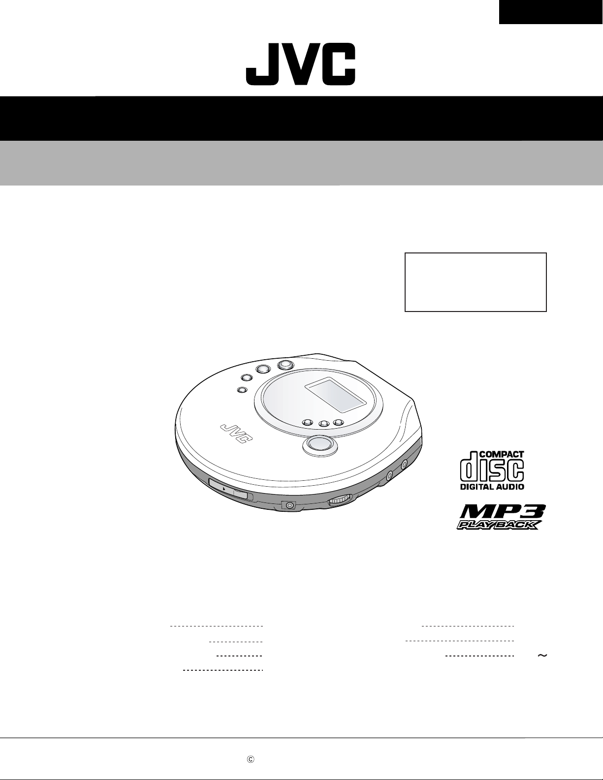
SERVICE MANUAL
PORTABLE CD PLAYER
XL-PM20SL
Area suffix
C -------------------------- Canada
E ----------- Continental Europe
XL-PM20SL
Contents
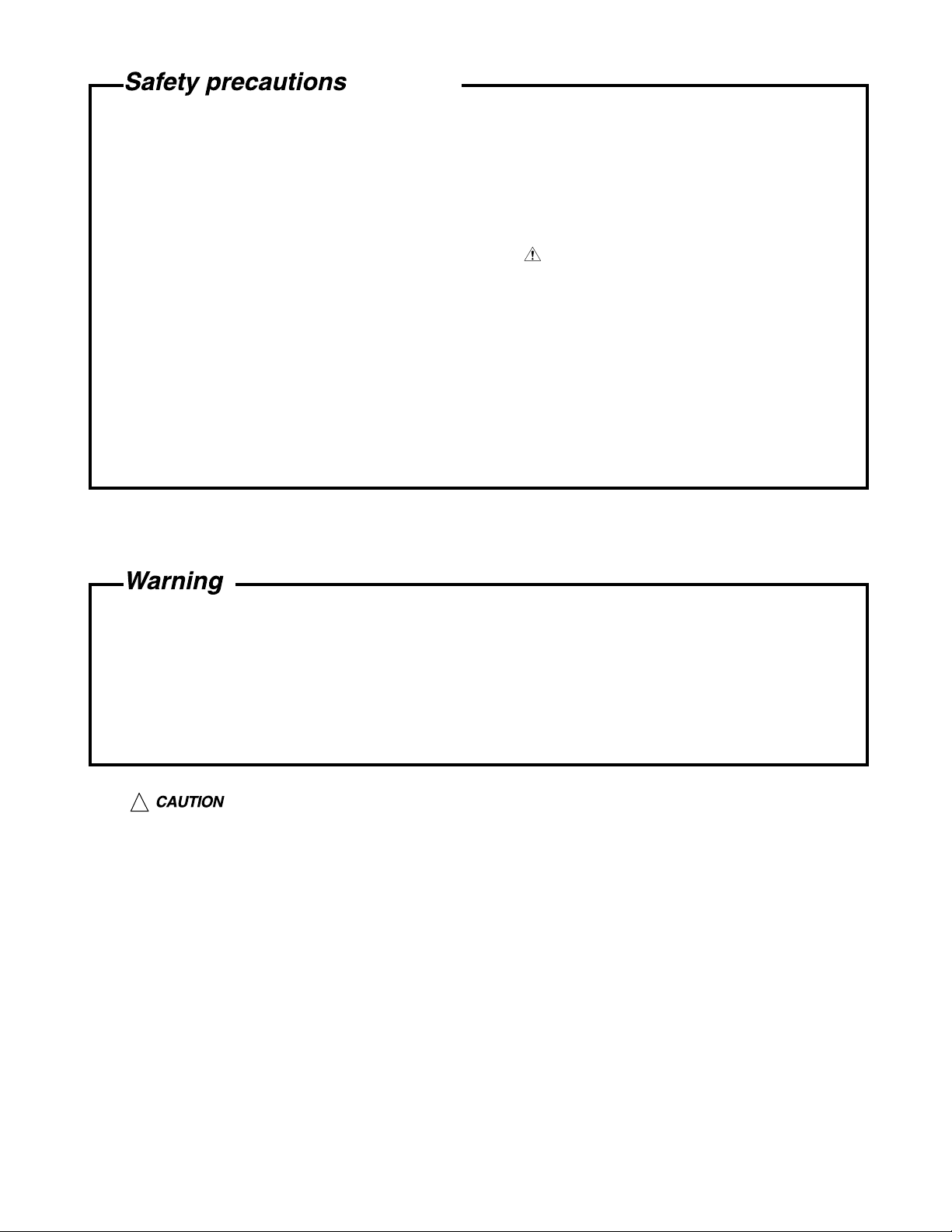
Safety precautions
Preventing static electricity
Important for laser products
Disassembly method
COPYRIGHT 2002 VICTOR COMPANY OF JAPAN, LTD.
1-2
1-4
1-5
1-6
Adjustment method
Trouble shooting
Description of major ICs
1-8
1-8
1-9 17
No.21133
Aug. 2002
Page 2
XL-PM20SL
1. This design of this product contains special hardware and many circuits and components specially for safety
purposes. For continued protection, no changes should be made to the original design unless authorized in
writing by the manufacturer. Replacement parts must be identical to those used in the original circuits. Services
should be performed by qualified personnel only.
2. Alterations of the design or circuitry of the product should not be made. Any design alterations of the product
should not be made. Any design alterations or additions will void the manufacturer`s warranty and will further
relieve the manufacture of responsibility for personal injury or property damage resulting therefrom.
3. Many electrical and mechanical parts in the products have special safety-related characteristics. These
characteristics are often not evident from visual inspection nor can the protection afforded by them necessarily
be obtained by using replacement components rated for higher voltage, wattage, etc. Replacement parts which
have these special safety characteristics are identified in the Parts List of Service Manual. Electrical
components having such features are identified by shading on the schematics and by ( ) on the Parts List in
the Service Manual. The use of a substitute replacement which does not have the same safety characteristics
as the recommended replacement parts shown in the Parts List of Service Manual may create shock, fire, or
other hazards.
4. The leads in the products are routed and dressed with ties, clamps, tubings, barriers and the like to be
separated from live parts, high temperature parts, moving parts and/or sharp edges for the prevention of
electric shock and fire hazard. When service is required, the original lead routing and dress should be
observed, and it should be confirmed that they have been returned to normal, after re-assembling.
5. Leakage currnet check (Electrical shock hazard testing)
After re-assembling the product, always perform an isolation check on the exposed metal parts of the product
(antenna terminals, knobs, metal cabinet, screw heads, headphone jack, control shafts, etc.) to be sure the
product is safe to operate without danger of electrical shock.
Do not use a line isolation transformer during this check.
Plug the AC line cord directly into the AC outlet. Using a "Leakage Current Tester", measure the leakage
current from each exposed metal parts of the cabinet, particularly any exposed metal part having a return
path to the chassis, to a known good earth ground. Any leakage current must not exceed 0.5mA AC (r.m.s.).
Alternate check method
Plug the AC line cord directly into the AC outlet. Use an AC voltmeter having, 1,000 ohms per volt or more
sensitivity in the following manner. Connect a 1,500 10W resistor paralleled by a 0.15 F AC-type capacitor
between an exposed metal part and a known good earth ground.
Measure the AC voltage across the resistor with the AC
voltmeter.
Move the resistor connection to each exposed metal part,
particularly any exposed metal part having a return path to
the chassis, and meausre the AC voltage across the resistor.
Now, reverse the plug in the AC outlet and repeat each
measurement. Voltage measured any must not exceed 0.75 V
AC (r.m.s.). This corresponds to 0.5 mA AC (r.m.s.).
0.15 F AC TYPE
1500 10W
Good earth ground
AC VOLTMETER
(Having 1000
ohms/volts,
or more sensitivity)
Place this
probe on
each exposed
metal part.
!
1. This equipment has been designed and manufactured to meet international safety standards.
2. It is the legal responsibility of the repairer to ensure that these safety standards are maintained.
3. Repairs must be made in accordance with the relevant safety standards.
4. It is essential that safety critical components are replaced by approved parts.
5. If mains voltage selector is provided, check setting for local voltage.
Burrs formed during molding may
be left over on some parts of the
chassis. Therefore, pay attention to
such burrs in the case of
preforming repair of this system.
In regard with component parts appearing on the silk-screen printed side (parts side) of the PWB diagrams, the
parts that are printed over with black such as the resistor ( ), diode ( ) and ICP ( ) or identified by the " "
mark nearby are critical for safety.
(This regulation does not correspond to J and C version.)
1-2
Page 3
XL-PM20SL
(U.K only)
1. This design of this product contains special hardware and many circuits and components specially
for safety purposes. For continued protection, no changes should be made to the original
design unless authorized in writing by the manufacturer. Replacement parts must be identical to
those used in the original circuits.
2. Any unauthorised design alterations or additions will void the manufacturer's guarantee ; furthermore the
manufacturer cannot accept responsibility for personal injury or property damage resulting therefrom.
3. Essential safety critical components are identified by ( ) on the Parts List and by shading on the
schematics, and must never be replaced by parts other than those listed in the manual. Please note
however that many electrical and mechanical parts in the product have special safety related
characteristics. These characteristics are often not evident from visual inspection. Parts other than
specified by the manufacturer may not have the same safety characteristics as the recommended
replacement parts shown in the Parts List of the Service Manual and may create shock, fire, or
other hazards.
4. The leads in the products are routed and dressed with ties, clamps, tubings, barriers and the
like to be separated from live parts, high temperature parts, moving parts and/or sharp edges
for the prevention of electric shock and fire hazard. When service is required, the original lead
routing and dress should be observed, and it should be confirmed that they have been returned
to normal, after re-assembling.
1. Service should be performed by qualified personnel only.
2. This equipment has been designed and manufactured to meet international safety standards.
3. It is the legal responsibility of the repairer to ensure that these safety standards are maintained.
4. Repairs must be made in accordance with the relevant safety standards.
5. It is essential that safety critical components are replaced by approved parts.
6. If mains voltage selector is provided, check setting for local voltage.
!
Burrs formed during molding may be left over on some parts of the chassis. Therefore,
pay attention to such burrs in the case of preforming repair of this system.
1-3
Page 4

XL-PM20SL
Preventing static electricity
1. Grounding to prevent damage by static electricity
Electrostatic discharge (ESD), which occurs when static electricity stored in the body, fabric, etc. is discharged,
can destroy the laser diode in the traverse unit (optical pickup). Take care to prevent this when performing repairs.
2. About the earth processing for the destruction prevention by static electricity
Static electricity in the work area can destroy the optical pickup (laser diode) in devices such as CD players.
Be careful to use proper grounding in the area where repairs are being performed.
2-1 Ground the workbench
Ground the workbench by laying conductive material (such as a conductive sheet) or an iron plate over it
before placing the traverse unit (optical pickup) on it.
2-2 Ground yourself
Use an anti-static wrist strap to release any static electricity built up in your body.
(caption)
Anti-static wrist strap
Conductive material
(conductive sheet) or iron plate
3. Handling the optical pickup
In order to maintain quality during transport and before installation, both sides of the laser diode on the
1.
replacement optical pickup are shorted. After replacement, return the shorted parts to their original condition.
(Refer to the text.)
Do not use a tester to check the condition of the laser diode in the optical pickup. The tester's internal power
2.
source can easily destroy the laser diode.
4. Handling the traverse unit (optical pickup)
1.
Do not subject the traverse unit (optical pickup) to strong shocks, as it is a sensitive, complex unit.
2.
Remove solder of the short land on the flexible wire after replacing the optical pickup. For specific details, refer
to the replacement procedure in the text. Remove the anti-static pin when replacing the traverse unit.
Be careful not to take too long a time when attaching it to the connector.
3.
Handle the flexible wire carefully as it may break when subjected to strong force.
4.
It is not possible to adjust the semi-fixed resistor that adjusts the laser power. Do not turn it.
5. Attention when traverse unit is decomposed
*Please refer to "Disassembly method".
Main board Flexible wire
Apply solder to the short land before the flexible wire is disconnected
from the connector on the main board.
(If the flexible wire is disconnected without applying solder, the CD
pickup may be destroyed by static electricity.)
In the assembly, be sure to remove solder from the short land after
connecting the flexible wire.
1-4
Short land
Page 5
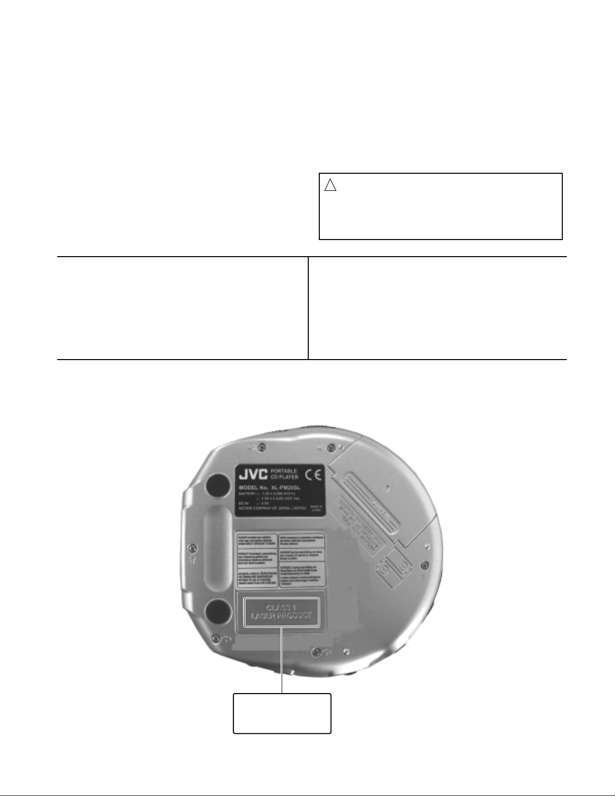
Important for laser products
XL-PM20SL
1.CLASS 1 LASER PRODUCT
2.DANGER : Invisible laser radiation when open and inter
lock failed or defeated. Avoid direct exposure to beam.
3.CAUTION : There are no serviceable parts inside the
Laser Unit. Do not disassemble the Laser Unit. Replace
the complete Laser Unit if it malfunctions.
4.CAUTION : The compact disc player uses invisible
laserradiation and is equipped with safety switches
whichprevent emission of radiation when the drawer is
open and the safety interlocks have failed or are de
feated. It is dangerous to defeat the safety switches.
VARNING : Osynlig laserstrålning är denna del är öppnad
och spårren är urkopplad. Betrakta ej strålen.
VARO : Avattaessa ja suojalukitus ohitettaessa olet
alttiina näkymättömälle lasersäteilylle.Älä katso
säteeseen.
5.CAUTION : If safety switches malfunction, the laser is able
to function.
6.CAUTION : Use of controls, adjustments or performance of
procedures other than those specified herein may result in
hazardous radiation exposure.
CAUTION
!
Please use enough caution not to
see the beam directly or touch it
in case of an adjustment or operation
check.
ADVARSEL : Usynlig laserstråling ved åbning , når
sikkerhedsafbrydere er ude af funktion. Undgå
udsættelse for stråling.
ADVARSEL : Usynlig laserstråling ved åpning,når
sikkerhetsbryteren er avslott. unngå utsettelse
for stråling.
REPRODUCTION AND POSITION OF LABELS
CLASS 1
LASER PRODUCT
1-5
Page 6
XL-PM20SL
Disassembly method
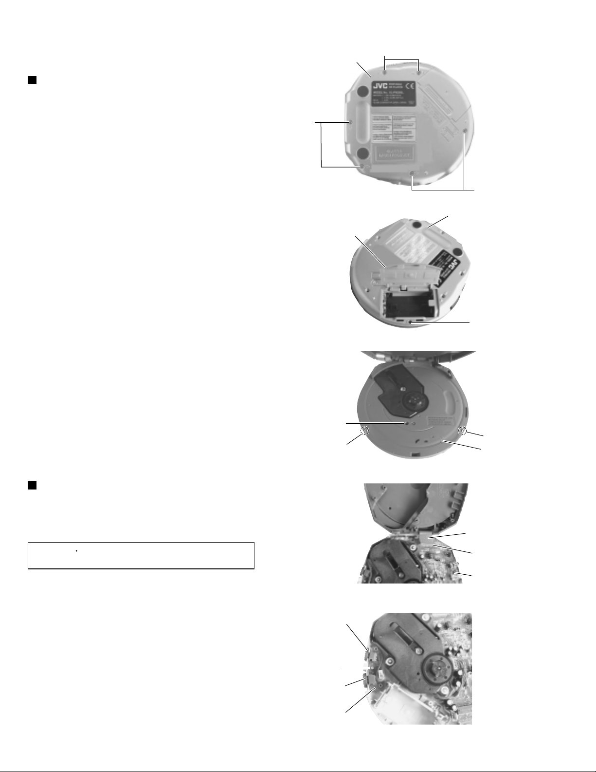
Removing the bottom cabinet
(See Figs. 1 to 3.)
From the bottom side of the main body, remove the
1.
six screws A from the bottom cabinet. (See Fig.1.)
Open the battery door, then remove the screw B
2.
from the bottom cabinet. (See Fig.2.)
From the top side of the main body, pay attention to
3.
remove the screw C from the middle cabinet before
next procedure. (See Fig.3.)
Disengage the claws a of the bottom cabinet from
4.
the middle cabinet and then remove the bottom
cabinet.
Bottom cabinet
A
Battery door
A
A
Fig. 1
Bottom cabinet
B
Fig. 2
Removing the main parts
(See Figs. 4 to 10.)
1.
Disconnect the flexible wire from connector CN7 on
the main board. (See Fig.4.)
[Caution]
2.
Remove the HOLD & HBS slide knobs.
3.
Remove the HOLD & HBS board by releasing the
screw D. (See Fig.5.)
Pay attention not damage the flexible
wire during disconnection.
(See Fig.5.)
C
Claw a
HOLD slide knob
D
HBS slide knob
Claw a
Middle cabinet
Fig. 3
Flexible wire
CN7
Main board
Fig. 4
1-6
HOLD & HBS board
Fig. 5
Page 7

4.
Remove the battery plate "+" and battery plate "-"
from the bottom cabinet. (See Fig.6.)
5.
Remove the CD mechanism assembly together the
main board and HOLD & HBS board from bottom
cabinet.
XL-PM20SL
6.
Disconnect the CD mechanism wire from
connector CN2 on the main board. (See Fig. 7)
7.
Apply solder to short land section a on the flexible
wire. (See Fig.8.)
[Caution] Be sure to apply solder in order to
short land section a on the flexible
wire before removing the flexible
wire from the main board.
(See Fig. 8.)
If the flexible wire is removed without
applying this solder, the CD pickup
may be damaged.
8.
After soldering, disconnect the flexible wire from
connector CN1 on the main board. (See Fig.9.)
[Caution] After re-connecting the flexible
wire, be sure to remove the solder
from short land a.
9.
Final disassembly condition. (See Fig.10.)
[Caution]
No serviceable parts are provided
inside AC adaptor. Do not open it.
Battery plate"+"
Main board
Short land section a
CD mechanism assembly
Battery plate"-"
Fig. 6
Fig. 7
Flexible wire
Fig. 8
Bottom cabinet
CN2
CD mechanism
wire
Main board
Main board
HOLD & HBS board
Flexible wire
CD mechanism assembly
Middle cabinet
Fig. 9
Fig. 10
CN1
Main board
HOLD & HBS board
Bottom cabinet
1-7
Page 8

XL-PM20SL
Adjustment method
Measuring instructions required for
adjustment
Oscilloscope
1.
Jitter meter
2.
Measurement conditions
Power supply voltage
AC120V/60Hz (C version)
AC230V/50Hz (B/E version)
Electrical adjustment
Perform adjust focus bias adjust only.
Connect an oscilloscope and jitter meter to the test
1.
point RF (Pin 63 of U3 KA9225) and VR (Pin 55 of
U3 KA9225).
Locations of the test points are shown on fig.1.
VR
RF
U3
Main board
(Reverse side)
Load the disc, then keep door switch short (Door
2.
close).
Press the PLAY button.
3.
MICOM auto adjust for an optimum waveform eye
4.
pattern with an amplitude of 1.0 to 1.3V.
The waveform of the eye pattern is shown on fig.2.
Trouble shooting
PROBLEM
No sound
Disc is inserted
but number of
tracks and
playing time are
not displayed.
No ANTI-SHOCK
PAUSE function is ON.
Without press PLAY key one.
VOLUME control is at its minimum position.
CD deck is empty.
Door is open.
Hold key set ON
Disc is inserted upside down.
Disc is dirty.
Disc is scratched.
Disc is seriously warped.
A non-standard disc is inserted.
Moisture has formed inside the CD deck.
ANTI-SHOCK OFF
POSSIBLE CASE
Fig.1
Fig.2
REMEDY
Press PLAY button to resume.
Press PLAY key to start power and play.
Set the VOLUME control to a proper sound level.
Insert a disc and play.
Close the door.
Switch hold key to OFF
Insert disc correctly
Wipe clean with soft cloth
Use a new disc.
Use a new disc.
Use only brand name disc.
Wait about 20 to 30 minutes.
Press ANTI-SHOCK key once to start function.
1-8
Page 9

Description of major ICs
S3C821AXZZ-TWRA (U1) : Central processing unit
1.Terminal layout
SEG19
SEG18
SEG17
SEG16
SEG15
SEG14
SEG13
SEG12
SEG11
SEG10
SEG9
SEG8
SEG7
SEG6
NC
80 79 78 77 76 75 74 73 72 71 70 69 68 67 66 65 64 63 62 61
SEG5
SEG4
SEG3
SEG2
XL-PM20SL
SEG1
1
NC
2
NC
3
NC
4
NC
5
NC
6
NC
7
MLAT
8
MINT
9
MDOUT
XOUT
NC
NC
RESET
MCK
M DATA
MLT
10
11
12
13
14
15
16
17
18
19
20
21 22 23 24 25 26 27 28 29 30 31 32 33 34 35 36 37 38 39 40
SCOR
SSENSE
K1
DSENSE
AVREF(VDD)
(9225+9288+9276)
K2
BATT
REMO
VDD1(VDD)
VSS1(GND)
XIN(8 MHz)
TEST(GND)
LA4533M (U4) : Audio amplifier
2.Block diagram1.Terminal layout
10
1
6
(POWER SWITCH)
5
(PRE GND)
S3C821A-XX
80-TQFP-1212
SUBQ
SQCK
GND
1
2IN1
3
4IN2
CDMUTE
POWER
SWITCH
AVSS(GND)
P/SW
XRST
FOK
CLOSE
Amp 1
Amp 2
POFF
HOLDSW
MUTE
CIRCUIT
AMUTE
HPMUTE
60
59
58
57
56
55
54
53
52
51
50
49
48
47
46
45
44
43
42
41
CLVX1X2
M/SW
10
(MUTE SWITCH)
9
OUT1
GND
8
(POWER GND)
7
OUT2
SEG0
COM0
COM1
COM2
COM3
COM4
COM5
COM6
COM7
VDD2(VDD)
VSS2(GND)
VLC1
ESP OPT2
ESP OPT1
ESP OPT0
BEEP
OPT2
OPT1(LCD)
OPT0(KICK)
NC
GM71C17403CJ-6 (U8) : DRAM
1.Terminal layout
VSSD3D2
2625242322
12345
VCC
CASOEA9
D1
D0
WE
RAS
21
6
NC
A8A7A6A5A4
1918171615
8
9
101112
A2
A1
A0
A10
14
13
A3
VCC VSS
5REF
BIAS
6
VCC
1-9
Page 10

XL-PM20SL
S5L9276X01-E0R0 (U5) : Decoder
1.Terminal layout
48
33
49
64
1
2.Block diagram
CD-MP3 Decoder Chip
(CD-ROM Decoder)
cdrUnit
32
17
16
Register
Set
dspUnit
IB
read
Channel
memUnit
(Memory Management Unit)
OB
write
Channel
ssp1611 Core +
CROM0,RAM0,
CROM1,RAM1
OBL
read
Channel
PROM,
OBR
read
Channel
difUnit
(DAC I/F)
Host
Channel
hifUnit
(Host Interface)
ckgUnit
DRAM Bandwidth Estimated
- 1.9M words/sec
DRAM Controller
1M x 4 bits DRAM
3. Pin function
Pin No. Symbol I/O Function
1
2
3
4
5
6
7
8
9
10
11
12
13
14
15
VDD
XI
XO
XOUT
CLK
RESETB
PLL0VDDA
PLL0VSSA
PLL0VBBA
FILTER0
PLL1VDDA
PLL1VSSA
PLL1VBBA
FILTER1
PBYPASS
-
Digital power
I
X'tal oscillator input (16.9344 MHz)
O
X'tal oscillator output
O
Buffered output of XO
I
System clock input
I
System reset active low
-
Analog power for PLL0
-
Analog ground for PLL0
-
Analog ground for PLL0
O
External capacitor port for PLL0
-
Analog power for PLL1
-
Analog ground for PLL1
-
Analog ground for PLL1
O
External capacitor port for PLL1
I
Tied to ground.
Host MCU
1-10
Page 11

Pin No. Symbol I/O Function
16
17
18
19
20
21
22
23
24
25
26
27
28
29
30
31
32
33
34
35
36
37
38
39
40
41
42
43
44
45
46
47
48
49
50
51
52
53
54
55
56
57
58
59
60
61
62
63
64
VSS
VDD
ACLKEXT
CDCLK
CDDATA
CDLRCK
CDBCK
CDC2PO
ACLK
BCLK
LRCK
ADAT
EMP
ETYPE
NC
DA10
VSS
VDD
MCUCLK
MDAT
MCK
MLAT
MDO
MINT
SCAN_EN
TEST2
TEST1
TEST0
DDAT0
DDAT1
WEB
RASB
VSS
VDD
DDAT2
DDAT3
CASB
DA08
DA07
DA06
DA05
DA04
DA09
DA00
DA01
DA02
DA03
OEB
VSS
-
Digital ground
-
Digital power
I
External audio clock source (Not connect)
O
Clock output for CD DSP IC
I
Data from CD DSP IC
I
LRCK from CD DSP IC
I
BCK from CD DSP IC
I
C2PO from CD DSP IC
O
Audio clock to DAC clock input
O
BCLK to DAC
O
LRCK to DAC
O
Data to DAC
O
Emphasis ON/OFF (Not connect)
O
Indicates emphasis type (Not connect)
-
No used
O
Address output10 for DRAM
-
Digital ground
-
Digital power
O
Clock output for external MCU (Not connect)
I
Data input pin
I
Micom clock pin
I
Data latch input pin
O
Data from CD-MP3 to MCU
O
Interrupt output to MCU
O
Scan test enable
I
Tied to ground
I
Tied to ground
I
Tied to ground
I/O
Data0 bus for external DRAM
I/O
Data1 bus for external DRAM
O
Write enable for external DRAM
O
Row address for external DRAM
-
Digital ground
-
Digital power
I/O
Data2 bus for external DRAM
I/O
Data3 bus for external DRAM
O
Column address for external DRAM
O
Address output8 for DRAM
O
Address output7 for DRAM
O
Address output6 for DRAM
O
Address output5 for DRAM
O
Address output4 for DRAM
O
Address output9 for DRAM
O
Address output0 for DRAM
O
Address output1 for DRAM
O
Address output2 for DRAM
O
Address output3 for DRAM
O
Output to make data output to "Hi-Z at DRAM"
-
Digital ground
XL-PM20SL
1-11
Page 12

XL-PM20SL
KA9225 (U3) : RF
1.Terminal layout 2.Block diagram
49
64
48
1
33
16
17
32
EQO
EFMI
DCC1
DCC2
MCP
DCB
GND
FRSH
FSET
FLB
FGD
FDFCT
FSEO
FSI
ATO
TGU
EQI
RFO
RFM
RFM2
TESO
LPC
LPB
EQC
VCC
VREF
PDE
PDF
64
63
62
61
60
59
58
57
56
55
54
53
1
2
3
4
5
6
7
8
9
10
11
12
13
14
15
16
RF AGC &
EQ Control
Focus OK Detect
Defect Detect
Mirror Gen
Focus Servo Loop
-Gain & Phase
Compensation
-Focus Search
-Offset Adjust
-FZC Gen.
Micom Data Interface logic Decoder
Center
Voltage
APC. Laser
Control & LPC
Tracking Servo Loop
- Gain & Phase
Compensation
- Track Jump
- Offset Adjust
- TZC Gen.
Hardware logic
- Auto-Sequencer
- Fast Search
- Febias, Focus Servo,
Tracking Offset ADJ.
- Tracking Balance & Gain
Adjust
- Interruption Detect
- EFM Muting System
Tracking
Error
(RW) I/V
AMP
EFM
Comparator
PDB
PDD
52
51
RF & Focus
Error (CD-RW)
I/V AMP
Sled servo
& Kick Gen.
Spindle
Servo LPF
PDC
50
PDA
49
PD
48
LD
47
LPF2
46
45
LPF1
TEIO
44
TZC
43
ATSC
42
41
TEO
TEM
40
39
SLP
SLO
38
37
SLM
FEO
36
FEM
35
SPO
34
33
SPM
17
18
19
20
21
22
23
VDD
ISTAT
ISTAT1
MCK
MDATA
MLT
XRST
3. Pin function
Pin No. Symbol I/O Function
1
2
3
4
5
6
7
8
9
10
11
12
13
14
15
EQO
EFMI
DCC1
DCC2
MCP
DCB
GND
FRSH
FSET
FLB
FGD
FDFCT
FSEO
FSI
ATO
O
RF equalizer output (Not connect)
I
EFM slice input. (input impedance 47K)
O
Time constant connection output to detect defects
I
Time constant connection input to detect defects
I
CAP connection terminal for mirror hold
I
CAP terminal to limit defect detection
-
RF, servo ground
I
CAP connection terminal for focus search
I
Filter bias for focus, tracking, spindle (Not connect)
I
CAP terminal to make focus loop rising low band
I
Terminal to charge the high frequency gain of the focus loop
I
CAP connection terminal to integrate the focus error
O
Focus error output
I
Focus servo input
O
Shock level detect output (shock: L:state)
24
WDCK
25
CLVI
26
LOCK
27
ASY
28
EFM2
29
EFM
30
SSTOP
31
VSS
32
VDD
1-12
Page 13

Pin No. Symbol I/O Function
16
17
18
19
20
21
22
23
24
25
26
27
28
29
30
31
32
33
34
35
36
37
38
39
40
41
42
43
44
45
46
47
48
49
50
51
52
53
54
55
56
57
58
59
60
61
62
63
64
TGU
VDD
I STAT
I STAT 1
MCK
M DATA
MLT
XRST
WDCK
CLVI
LOCK
ASY
EFM2
EFM
SSTOP
VSS
VDD
SPM
SPO
FEM
FEO
SLM
SLO
SLP
TEM
TEO
ATSC
TZC
TEIO
LPF1
LPF2
LD
PD
PDA
PDB
PDC
PDD
PDF
PDE
VREF
VCC
EQC
LPB
LPC
TESO
RFM2
RFM
RFO
EQI
I
Time constant connection to charge the high frequency gain of the tracking loop.
-
Power supply for the servo
O
Internal status output pin (FOK, TRCNT)
O
Internal status output pin
I
Micom clock pin
I
Data input pin
I
Data latch input pin
I
Reset input pin
I
88.2kHz input terminal from DSP
I
Control output input terminal of DSP spindle
I
Sled run away prevention pin (L: sled off and tracking gain up)
I
Auto asymmetry control input terminal
O
Output for EFM pulse integration
O
EFM output terminal for RFO slice (to DSP)
I
PICK UP's maximum lead-in diameter position check pin
-
Digital ground
-
Digital power
I
Spindle amp inverting input pin
O
Spindle amp output pin
I
Focus servo amp inverting input pin
O
Focus servo amp output pin
I
Sled servo inverting input
O
Sled servo output
I
Sled servo non inverting input
I
Tracking servo amp inverting input pin
O
Tracking servo amp output pin
I
Anti-shock input pin
I
Tracking zero crossing input pin
I/O
Tracking error output & tracking servo input pin
I
Tracking error integration input terminal 1 (automatic control)
I
Tracking error integration input terminal 2 (automatic control)
O
APC AMP output pin
I
APC AMP input pin
I
Photo-diode A/C RF I/V amp1 inverting input pin
I
Photo-diode B/D RF I/V amp2 inverting input pin
I
Photo-diode A/C RF I/V amp1 inverting input pin
I
Photo-diode B/D RF I/V amp2 inverting input pin
I
Photo-diode F with tracking (F) I/V amp inverting input pin
I
Photo-diode E with tracking (E) I/V amp inverting input pin
O
(VCC + GND) /2 voltage reference output pin
-
RF part VCC power supply pin
I
AGC_equalize level control terminal and VCA input connection cap terminal
I
Laser power level control resistance terminal (Not connect)
I
Laser power control tracking summing signal integration terminal (Not connect)
O
Tracking error summing signal (Not connect)
I
RF summing amp 2x filter ON/OFF
I
RF summing amp inverting input terminal
O
RF summing amp output terminal
I
RFO dc control input terminal (use by MIROR, FOK, AGC&EQ terminals)
XL-PM20SL
1-13
Page 14

XL-PM20SL
S5L9288D01-TORO (U2) : DSP
1.Terminal layout 2.Block diagram
4160
4061
VCO1LP
VCO2LP
EFMI
LOCK, SMEF
80
1
21
20
SMON, SMDP
SMDS, WDCK
TESTV
WFCK, RFCK
C4M
XIN
I STAT
MLT, MDAT
MCK, MUTE
DPLL
CLV
Servo
Timing
Generator
Micom
Interface
SOSI
SQCK
SQDT
SBCK
SBDT
Subcode
Out
EFM
Demodulator
ECC
16K
SRAM
Address
Generator
C2PO
Interpolator
Encoder Decoder
DATX
Digital
Out
I/O
Interface
DRAM
Interface
Digital
Filter
1-bit
DAC
PWM
LPF
JITB
3. Pin function
Pin No. Symbol I/O Function
1
2
3
4
5
6
7
8
9
10
11
12
13
14
15
16
17
18
19
20
21
22
23
24
25
26
27
28
29
VDDAPLL
VSSAPLL
VBBAPLL
VCO1LF
VCO2LF
VSSDPLL
VDDDPLL
PBCK
VDDD1
XIN
XOUT
VSSD1
TEST0
EFMI
LOCK
SMEF
SMON
SMDP
SMSD
WDCK
VDD
TESTV
WFCK
LKFS
XRST
MLT
M DATA
MCK
I STAT
-
Analog power for DPLL
-
Analog ground for DPLL
-
Analog bulk bias ground for DPLL
O
Pump out for VCO1
O
Pump out for VCO2
-
Digital ground separated bulk bias for DPLL
-
Digital power separated bulk bias for DPLL
-
VCO 1/2 clock output (4.3218 MHz) (Not connect)
-
Digital power
I
X'tal oscillator input (16.9344 MHz)
O
X'tal oscillator output (Not connect)
-
Digital ground
I
Test input
I
EFM signal input
O
CLV servo locking status output
O
LPF time constant control of the spindle servo error signal
O
ON/OFF control signal for spindle servo
O
Phase control output for spindle motor drive
O
Speed control output for spindle motor drive
O
Word clock output (X1: 88.2kHz, X2: 176.4kHz)
-
Digital power
I
Various test input
O
Write base clock output (Not connect)
O
The lock status output of frame sync (Not connect)
I
System reset at "L"
I
Latch signal input from micom
I
Serial data input from micom
I
Serial data receiving clock input from micom
O
The internal status output to micom
A9 - A0
D3 - D0
CAS1,CAS0
RAS, WE
LCHOUT
RCHOUT
VHALE
VREF
1-14
Page 15

Pin No. Symbol I/O Function
30
31
32
33
34
35
36
37
38
39
40
41 - 43
44
45
46
47
48
49
50
51
52
53
54
55
56
57
58
59
60
61
62
63
64
65
66
67
68
69
70
71
72
73
74
75
76
77
78
79
80
SOSI
SQCK
SQDT
LCHOUT
VDDADAC
VHALF
VREF
VSSADAC
RCHOUT
VDDDDAC
VSS
TEST1 - 3
MUTE
SBCK
SBDT
C4M
VSSD2
VDD
DATX
JITB
C2PO
RFCK
MINT0
MINT1
MINT2
MINT3
MINT4
MINT5
VSS
VDD
D0
D1
WE
RAS
D2
D3
CAS0
CAS1(A10)
A8
A7
A6
A5
A4
A9
A0
A1
A2
A3
VSS
I/O
Subcode sync signal (S0+S1) output
I
Subcode-Q data transferring bit clock input
O
Subcode-Q data serial output
O
Left-channel audio output through DAC
-
Analog power for DAC
O
Reference voltage output for bypass
O
Reference voltage output for bypass
-
Analog ground for DAC
O
Right-channel audio output through DAC
-
Digital power for DAC
-
Digital ground for DAC
I
Test input
I
System mute at "H"
I
Subcode data transferring bit clock
I/O
Subcode data serial output (Not connect)
O
4.2336 MHz clock output (Not connect)
-
Digital ground
-
Digital power
O
Digital audio data output (Not connect)
I/O
Internal SRAM jitter margin status output (Not connect)
O
C2 pointer output
I/O
Read base clock output
I/O
Monitoring signal output
I/O
Monitoring signal output
I/O
Monitoring signal output
I/O
Monitoring signal output
I/O
Monitoring signal output
I/O
Monitoring signal output
-
Digital ground
-
Digital power
I/O
DRAM data input/output0
I/O
DRAM data input/output1
O
DRAM write enable output (active low)
O
DRAM row address selection output (active low)
I/O
DRAM data input/output2
I/O
DRAM data input/output3
O
DRAM column address selection output 0 (active low)
O
DRAM column address selection output 1 (active low)
O
DRAM address output8
O
DRAM address output7
O
DRAM address output6
O
DRAM address output5
O
DRAM address output4
O
DRAM address output9
O
DRAM address output0
O
DRAM address output1
O
DRAM address output2
O
DRAM address output3
-
Digital ground
XL-PM20SL
1-15
Page 16

XL-PM20SL
BD7920KS (U6) : Servo driver
1.Terminal layout
2942
43
56
1
2.Block diagram
43
SPRT
44
SOFT
45
DC IN
REGB
46
REGO
47
48
MIDOUT
28
15
14
DPG3
DPG2
CH1+
CH1-
CH2+
CH2-
PVCC
PVCC
CH3+
CH3-
42 41 40 39 38 37 36 35 34 33 32 31 30 29
REG/SW
PRE-DR PRE-DR
VSYS
Detector
PRE-DR PRE-DR
CH4+
+
-
+
-
+
-
CH4-
DPG1
DCT
28
N.C
FIL4
27
FIL3
26
FIL2
25
24
FIL1
23
VREF
49
DSW
50
PG1
51
PG2
52
USW
53
VSYS
54
SSW
55
VSUB
56
LG
3. Pin function
VSUB
-0.3V
PREG1
TSD
SYSTEM
ON
WP
PREG2
UP/DOWN
CONVERTER
VG
CONV
1 2 3 4 5 6 7 8 9 10 11 12 13 14
VG
+
-
-
SUB
CONV
+
-
EI
EO
+
-
SUBNF
SUBEO
OSC
RSTIN
PCT
+
+
-
OSC
Internal 1/2
Frequency
SYSTEM
OFF
RSTOUT
Pin No. Symbol Function
1
2
3
4
5
6
7
VG
EI
EO
SUBNF
SUBEO
RSTIN
PCT
Power MOS driving circuit power input pin
Voltage UP/DOWN DC/DC converter error amplifier input pin
Voltage UP/DOWN DC/DC converter error amplifier output pin
Microcomputer power error amplifier input pin
Microcomputer power error amplifier output pin (Not connect)
Reset power setting input pin
Power triangular wave output pin
MUTE1
OFF
MUTE34
MUTE1
MUTE34
22
21
20
19
18
17
16
15
VDD
DPREG
CH4
CH3
CH2
CH1
CLK
MIDFIL
1-16
Page 17

Pin No. Symbol Function
8
9
10
11
12
13
14
15
16
17
18
19
20
21
22
23
24
25
26
27
28
29
30
31
32
33
34
35
36
37
38
39
40
41
42
43
44
45
46
47
48
49
50
51
52
53
54
55
56
PREG1
PREG2
WP
RSTOUT
OFF
MUTE1
MUTE34
MIDFIL
CLK
CH1
CH2
CH3
CH4
DPREG
VCC
VREF
FIL1
FIL2
FIL3
FIL4
N.C.
DCT
DPG1
CH4-
CH4+
CH3CH3+
PVCC
PVCC
CH2CH2+
CH1CH1+
DPG2
DPG3
SPRT
SOFT
DC_IN
REGB
MIDOUT
REGO
DSW
PG1
PG2
USW
VSYS
SSW
VSUB
LG
Power control pre-ground
Power control pre-ground
DC/DC converter start pin
Reset detection output pin
DC/DC converter OFF pin
CH1 mute pin
CH34 mute pin
ESP power filter pin
External clock input pin
CH1 input pin
CH2 input pin
CH3 input pin
CH4 input pin
Driver pre-ground
Pre power input pin
Reference voltage input pin
CH1 filter pin
CH2 filter pin
CH3 filter pin
CH4 filter pin
Not connect
Driver triangular wave output pin
Driver POW ground
CH4 negative output pin
CH4 positive output pin
CH3 negative output pin
CH3 positive output pin
Power system power supply pin
Power system power supply pin
CH2 negative output pin
CH2 positive output pin
CH1 negative output pin
CH1 positive output pin
Driver POW ground
Driver POW ground
Power-off time constant setting pin
Soft start setting pin
AC adapter power supply input pin
Regulator Tr. base pin
ESP power supply output pin (Not connect)
Primary side power supply input pin
Voltage UP/DOWN DC/DC converter coil driving pin 1
Power control POW ground
Power control POW ground
Voltage UP/DOWN DC/DC converter coil driving pin 2
System power supply output pin
Microcomputer DC/DC converter coil driving pin (Not connect)
Microcomputer power supply output pin (Not connect)
VG voltage UP coil driving pin
XL-PM20SL
1-17
Page 18

XL-PM20SL
VICTOR COMPANY OF JAPAN, LIMITED
AUDIO & COMMUNICATION BUSINESS DIVISION
PERSONAL & MOBILE NETWORK BUSINESS UNIT. 10-1,1Chome,Ohwatari-machi,maebashi-city,371-8543,Japan
No.21133
200208
 Loading...