

Page 1
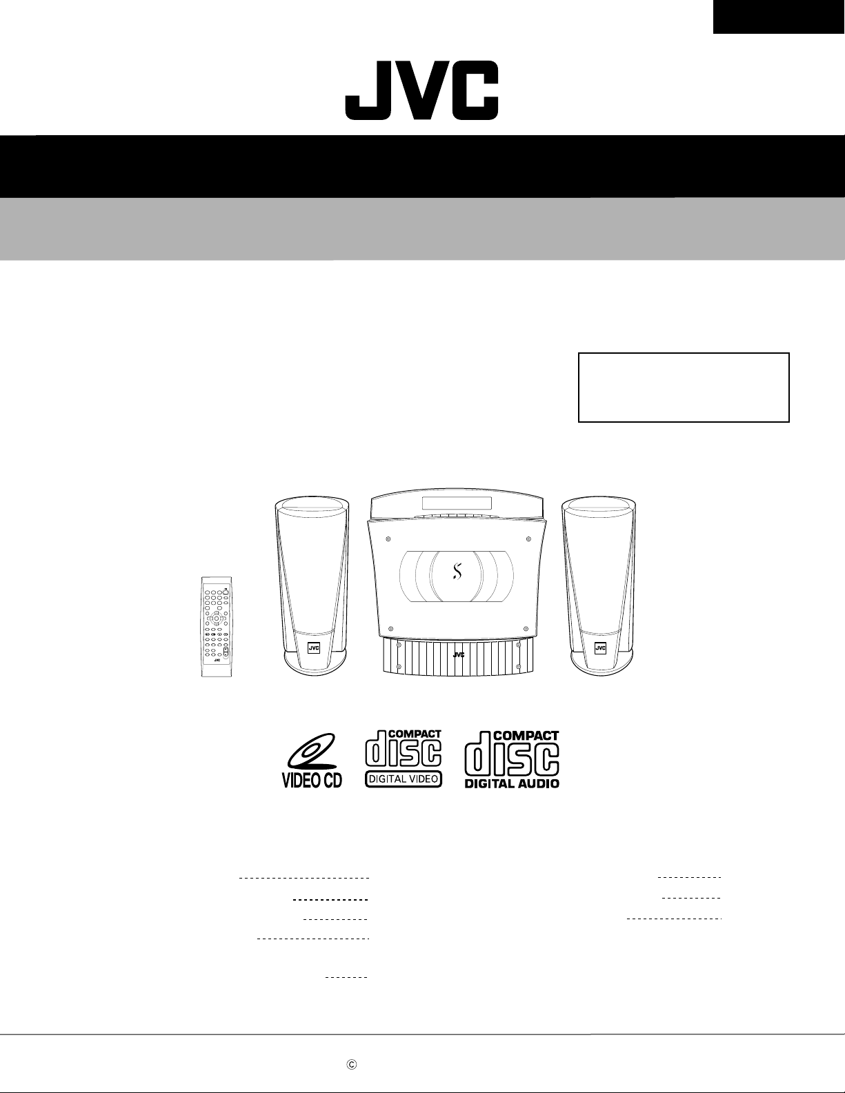
SERVICE MANUAL
COMPACT COMPONENT SYSTEM
VS-DT88V
Area suffix
UF ---------------------------- China
VS-DT88V
STANDBY/ON
123
FM/AM
4
6
5
MD/AUX
9
8
7
10
+10
CANCELMPX
VCD No. VCD No.
SET
ON
PBC
SCREEN
TREBLEBASSAHB PRO
PREV. CD SELECT NEXT
VIDEO
HIGH
INTRO
LIGHT&RETURN STILL
CLOCK
SLEEPDIMMER
REPEAT
/TIMER
FM
PLAY
MODE
MODE
OPEN
DISPLAY
COLOR
/CLOSE
VOLUME
Contents
Safety precautions
Preventing static electricity
Important for laser products
Disassembly method
Flow of functional operation
until TOC read
1-2
1-3
1-4
1-5
1-15
COMPACT COMPONENT SYSTEM
SP-VSDT88VCA-VSDT88VSP-VSDT88V
Maintenance of laser pickup
Replacement of laser pickup
Description of major ICs
1-16
1-16
1-17~34
COPYRIGHT 2002 VICTOR COMPANY OF JAPAN, LTD.
No.21179
Sep. 2002
Page 2
VS-DT88V
1. This design of this product contains special hardware and many circuits and components specially for safety
purposes. For continued protection, no changes should be made to the original design unless authorized in
writing by the manufacturer. Replacement parts must be identical to those used in the original circuits. Services
should be performed by qualified personnel only.
2. Alterations of the design or circuitry of the product should not be made. Any design alterations of the product
should not be made. Any design alterations or additions will void the manufacturer`s warranty and will further
relieve the manufacture of responsibility for personal injury or property damage resulting therefrom.
3. Many electrical and mechanical parts in the products have special safety-related characteristics. These
characteristics are often not evident from visual inspection nor can the protection afforded by them necessarily
be obtained by using replacement components rated for higher voltage, wattage, etc. Replacement parts which
have these special safety characteristics are identified in the Parts List of Service Manual. Electrical
components having such features are identified by shading on the schematics and by ( ) on the Parts List in
the Service Manual. The use of a substitute replacement which does not have the same safety characteristics
as the recommended replacement parts shown in the Parts List of Service Manual may create shock, fire, or
other hazards.
4. The leads in the products are routed and dressed with ties, clamps, tubings, barriers and the like to be
separated from live parts, high temperature parts, moving parts and/or sharp edges for the prevention of
electric shock and fire hazard. When service is required, the original lead routing and dress should be
observed, and it should be confirmed that they have been returned to normal, after re-assembling.
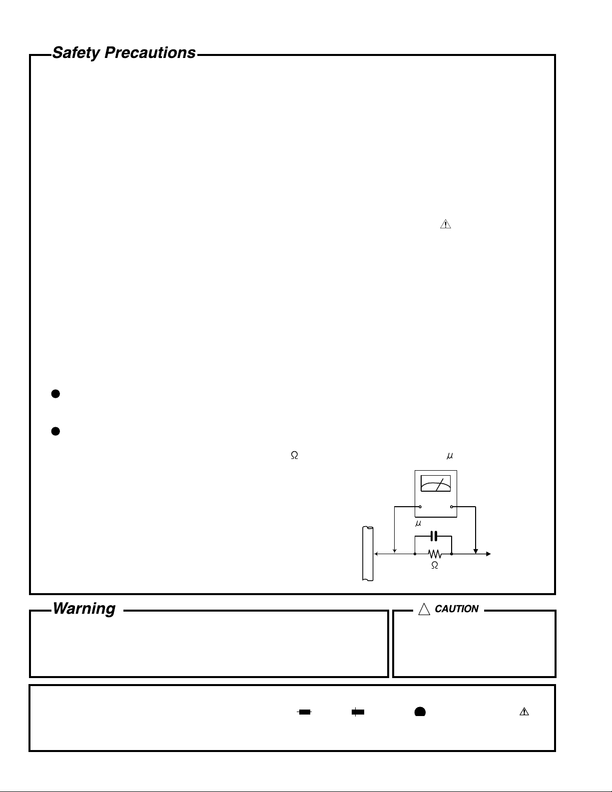
5. Leakage currnet check (Electrical shock hazard testing)
After re-assembling the product, always perform an isolation check on the exposed metal parts of the product
(antenna terminals, knobs, metal cabinet, screw heads, headphone jack, control shafts, etc.) to be sure the
product is safe to operate without danger of electrical shock.
Do not use a line isolation transformer during this check.
Plug the AC line cord directly into the AC outlet. Using a "Leakage Current Tester", measure the leakage
current from each exposed metal parts of the cabinet, particularly any exposed metal part having a return
path to the chassis, to a known good earth ground. Any leakage current must not exceed 0.5mA AC (r.m.s.).
Alternate check method
Plug the AC line cord directly into the AC outlet. Use an AC voltmeter having, 1,000 ohms per volt or more
sensitivity in the following manner. Connect a 1,500 10W resistor paralleled by a 0.15 F AC-type capacitor
between an exposed metal part and a known good earth ground.
Measure the AC voltage across the resistor with the AC
voltmeter.
Move the resistor connection to each exposed metal part,
particularly any exposed metal part having a return path to
the chassis, and meausre the AC voltage across the resistor.
Now, reverse the plug in the AC outlet and repeat each
measurement. Voltage measured any must not exceed 0.75 V
AC (r.m.s.). This corresponds to 0.5 mA AC (r.m.s.).
0.15 F AC TYPE
1500 10W
Good earth ground
AC VOLTMETER
(Having 1000
ohms/volts,
or more sensitivity)
Place this
probe on
each exposed
metal part.
!
1. This equipment has been designed and manufactured to meet international safety standards.
2. It is the legal responsibility of the repairer to ensure that these safety standards are maintained.
3. Repairs must be made in accordance with the relevant safety standards.
4. It is essential that safety critical components are replaced by approved parts.
5. If mains voltage selector is provided, check setting for local voltage.
Burrs formed during molding may
be left over on some parts of the
chassis. Therefore, pay attention to
such burrs in the case of
preforming repair of this system.
In regard with component parts appearing on the silk-screen printed side (parts side) of the PWB diagrams, the
parts that are printed over with black such as the resistor ( ), diode ( ) and ICP ( ) or identified by the " "
mark nearby are critical for safety.
(This regulation does not correspond to J and C version.)
1-2
Page 3
VS-DT88V
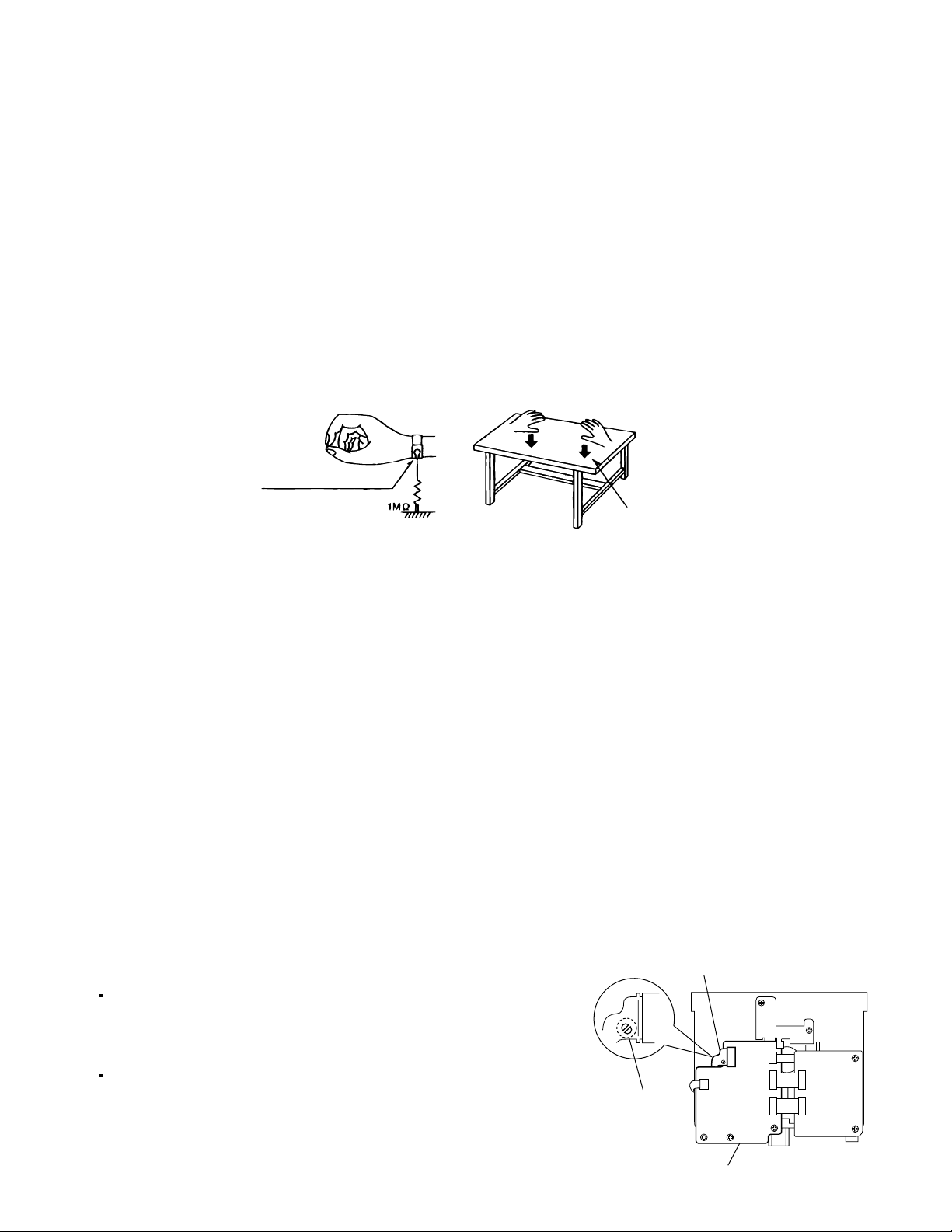
Preventing static electricity
1. Grounding to prevent damage by static electricity
Electrostatic discharge (ESD), which occurs when static electricity stored in the body, fabric, etc. is discharged,
can destroy the laser diode in the traverse unit (optical pickup). Take care to prevent this when performing repairs.
2. About the earth processing for the destruction prevention by static electricity
Static electricity in the work area can destroy the optical pickup (laser diode) in devices such as CD players.
Be careful to use proper grounding in the area where repairs are being performed.
2-1 Ground the workbench
Ground the workbench by laying conductive material (such as a conductive sheet) or an iron plate over it
before placing the traverse unit (optical pickup) on it.
2-2 Ground yourself
Use an anti-static wrist strap to release any static electricity built up in your body.
(caption)
Anti-static wrist strap
Conductive material
(conductive sheet) or iron plate
3. Handling the optical pickup
1.
In order to maintain quality during transport and before installation, both sides of the laser diode on the
replacement optical pickup are shorted. After replacement, return the shorted parts to their original condition.
(Refer to the text.)
2.
Do not use a tester to check the condition of the laser diode in the optical pickup. The tester's internal power
source can easily destroy the laser diode.
4. Handling the traverse unit (optical pickup)
1.
Do not subject the traverse unit (optical pickup) to strong shocks, as it is a sensitive, complex unit.
2.
Remove solder of the short land on the flexible wire after replacing the optical pickup. For specific details, refer
to the replacement procedure in the text. Remove the anti-static pin when replacing the traverse unit.
Be careful not to take too long a time when attaching it to the connector.
3.
Handle the flexible wire carefully as it may break when subjected to strong force.
4.
It is not possible to adjust the semi-fixed resistor that adjusts the laser power. Do not turn it.
5. Attention when traverse unit is decomposed
*Please refer to "Disassembly method" in the text for the CD pickup unit.
Flexible wire
Apply solder to the short land before the flexible wire is disconnected
from the connector CN601 on the
(If the flexible wire is disconnected without applying solder, the CD
pickup may be destroyed by static electricity.)
In the assembly, be sure to remove solder from the short land after
connecting the flexible wire.
CD servo board
.
CN601
Short land
CD servo board
1-3
Page 4
VS-DT88V
Important for laser products
1.CLASS 1 LASER PRODUCT
2.DANGER : Invisible laser radiation when open and inter
lock failed or defeated. Avoid direct exposure to beam.
3.CAUTION : There are no serviceable parts inside the
Laser Unit. Do not disassemble the Laser Unit. Replace
the complete Laser Unit if it malfunctions.
4.CAUTION : The compact disc player uses invisible
laserradiation and is equipped with safety switches
whichprevent emission of radiation when the drawer is
open and the safety interlocks have failed or are de
feated. It is dangerous to defeat the safety switches.
VARNING : Osynlig laserstrålning är denna del är öppnad
och spårren är urkopplad. Betrakta ej strålen.
VARO : Avattaessa ja suojalukitus ohitettaessa olet
alttiina näkymättömälle lasersäteilylle.Älä katso
säteeseen.
5.CAUTION : If safety switches malfunction, the laser is able
to function.
6.CAUTION : Use of controls, adjustments or performance of
procedures other than those specified herein may result in
hazardous radiation exposure.
CAUTION
!
Please use enough caution not to
see the beam directly or touch it
in case of an adjustment or operation
check.
ADVARSEL : Usynlig laserstråling ved åbning , når
sikkerhedsafbrydere er ude af funktion. Undgå
udsættelse for stråling.
ADVARSEL : Usynlig laserstråling ved åpning,når
sikkerhetsbryteren er avslott. unngå utsettelse
for stråling.
REPRODUCTION AND POSITION OF LABELS
WARNING LABEL
CLASS 1
LASER PRODUCT
CAUTION: Invisible laser
radiation when open and
interlock failed or defeated.
AVOID DIRECT EXPOSURE
TO BEAM. (e)
ADVARSEL: Usynlig laserstråling ved åbning, når
sikkerhedsafbrydere er ude
af funktion. Undgåudsættelse for stråling. (d)
interlock failed or defeated.
AVOID DIRECT EXPOSURE
TO BEAM. (e)
CAUTION: Invisible laser
radiation when open and
ADVARSEL: Usynlig laser-
stråling ved åbning, når
sikkerhedsafbrydere er ude
af funktion. Undgåudsæt-
telse for stråling. (d)
VARNING: Osynlig laser-
strålning när denna del är
öppnad och spärren är
urkopplad. Betrakta ej
strålen. (s)
VARO: Avattaessa ja
suojalukitus ohitettaessa
oleta lttiina näkymättö-
mälle lasersäteilylle.
Älä katso
säteeseen. (f)
VARNING: Osynlig laserstrålning när denna del är
öppnad och spärren är
urkopplad. Betrakta ej
strålen. (s)
VARO: Avattaessa ja
suojalukitus ohitettaessa
oleta lttiina näkymättömälle lasersäteilylle.
Älä katso
säteeseen. (f)
1-4
Page 5
VS-DT88V
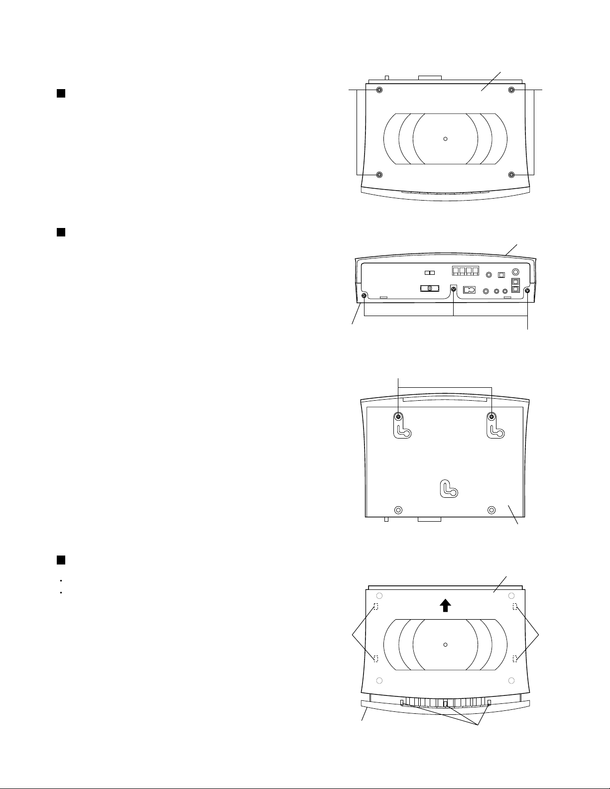
Disassembly method
<Main body section>
Removing the top lens (See Fig. 1.)
From the top side of the main body, remove the
four screws A attaching the top lens.
Removing the bottom panel
(See Figs. 2 and 3.)
1.
From the rear side of the main body, remove the
three screws B attaching the bottom panel.
(See Fig.2.)
2.
From the bottom side of the main body, remove the
two screws C attaching the bottom panel.
(See Fig.3.)
3.
Remove the bottom panel in an upward direction.
Top lens
AA
Fig.1
Top panel
Bottom panel
B
Fig.2
C
Removing the top panel (See Fig. 4.)
Remove the top lens.
Remove the bottom panel.
1.2.Slide the top panel toward the rear (direction of the
arrow), disengage it from the engagement sections
a of the front panel assembly and engagement
sections b of the bottom chassis.
Remove the top panel in an upward direction.
Bottom panel
Fig.3
Top panel
bb
Front panel assembly
Fig.4
a
1-5
Page 6
VS-DT88V
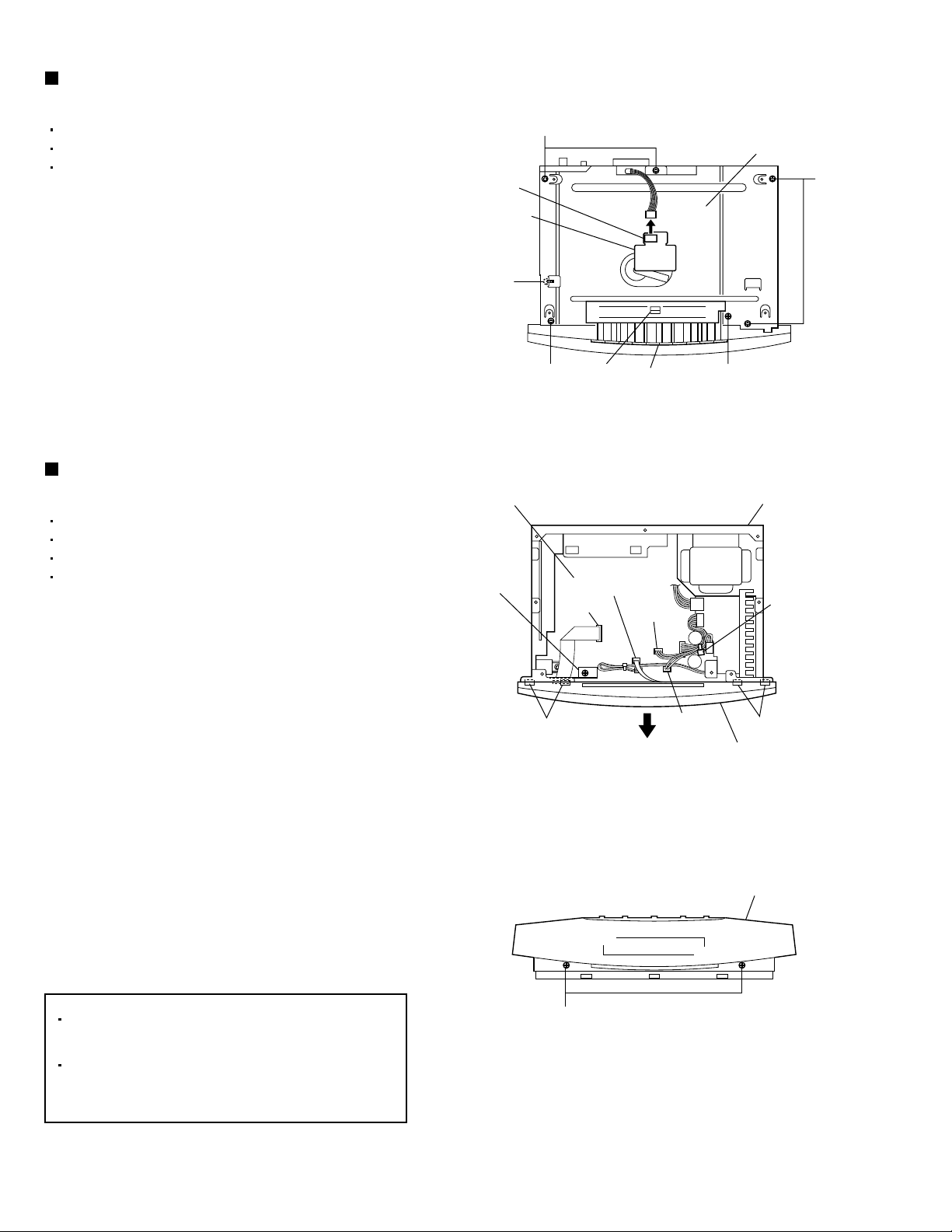
Removing the CD&Video CD
mechanism assembly (See Fig. 5.)
Remove the top lens.
Remove the bottom panel.
Remove the top panel.
1.
From the top side of the main body, disengage the
claw c of the CD&Video CD mechanism assembly
and then remove the push button.
2.
Remove the five screws D, screw E and screw F
attaching the CD&Video CD mechanism assembly.
3.
Disconnect the wire from connector CN801 on the
LED board.
4.
Remove the CD&Video CD mechanism assembly
in an upward direction.
Removing the front panel assembly
(See Figs. 6 and 7.)
Remove the top lens.
Remove the bottom panel.
Remove the top panel.
Remove the CD&Video CD mechanism assembly.
1.
Remove the tie band bundling the wires of the front
panel assembly. (See Fig.6.)
CN801
LED board
F
Main board
Wire holder
D
D
Claw c
CN171
CN183
Push button
Fig.5
CN182
CD&Video CD mechanism
assembly
D
E
Bottom chassis
Tie band
2.
Disconnect the wires from connectors CN106 and
CN182 on the main board. (See Fig.6.)
3.
Disconnect the card wires from connectors CN171
and CN183 on the main board. (See Fig.6.)
4.
Remove the wire holder holding the card wire of
the front panel assembly. (See Fig.6.)
5.
From the front side of the main body, remove the
two screws G attaching the front panel assembly.
(See Fig.7.)
6.
Disengage the claws d of the front panel assembly
from the bottom chassis and then remove the front
panel assembly in the direction of arrow.
(See Fig.6.)
[Reference]
Before attaching the front panel assembly,
pass the card wire of the front panel assembly
through the hole on the bottom chassis.
After attaching the front panel assembly,
bundling the card wire and wires of the front
panel assembly using a wire holder and tie
band.
Claws d
G
Fig.6
Fig.7
CN106
Front panel assembly
Claws d
Front panel assembly
1-6
Page 7
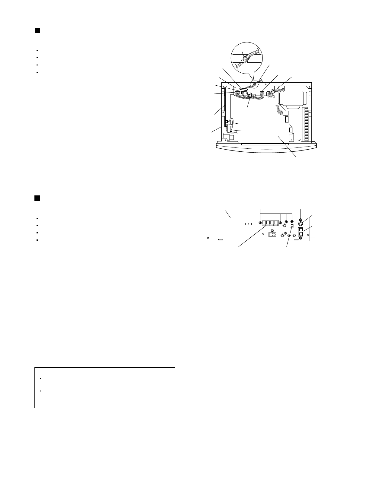
Removing the tuner board
(See Figs. 8 and 9.)
Remove the top lens.
Remove the bottom panel.
Remove the top panel.
Remove the CD&Video CD mechanism assembly.
1.
Disconnect the card wire from connector CN111 on
the main board. (See Fig.8.)
2.
Disconnect the wire from connector CN190 on the
tuner board. (See Fig.8.)
3.
From the rear side of the main body, remove the
two screws H attaching the FM/AM antenna
terminals on the tuner board. (See Fig.9.)
4.
Take out the tuner board from the bottom chassis.
Wire clamp
Speaker board
CN103
CN102
Tuner board
Bottom chassis
Notch
Tie band
CN190
CN111
VS-DT88V
CD & Video CD mechanism wire
CN101
Fig.8
Tie band
Main board
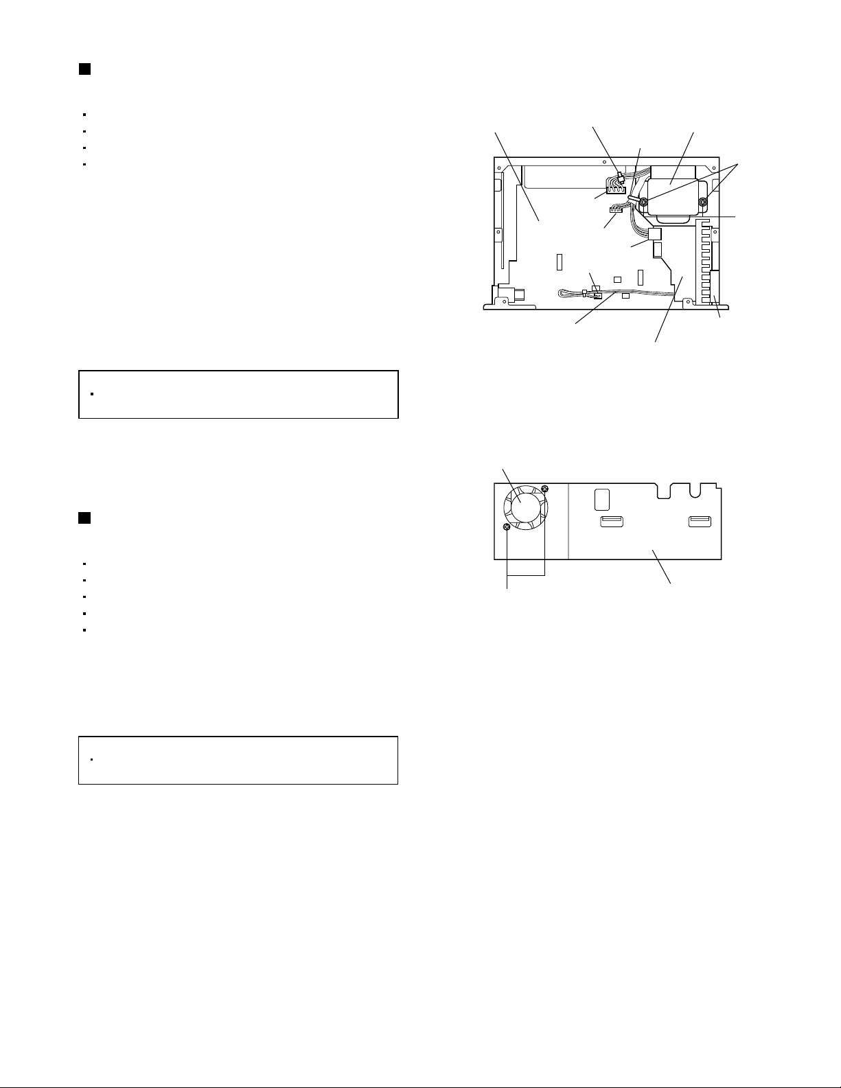
Removing the speaker board
(See Figs. 8 and 9.)
Remove the top lens.
Remove the bottom panel.
Remove the top panel.
Remove the CD&Video CD mechanism assembly.
1.
Remove the tie bands bundling the wires on the
speaker board. (See Fig.8.)
2.
Disengage the wire clamp bundling the wire of the
CD&Video CD mechanism wire. (See Fig.8.)
3.
Disconnect the wires from connectors CN101,
CN102 and CN103 on the speaker board.
(See Fig.8.)
4.
From the rear side of the main body, remove the
four screws J attaching the speaker/digital out
terminals on the speaker board. (See Fig.9.)
5.
Take out the speaker board from the bottom
chassis.
[Reference]
After connecting the wires to the speaker
board, bundle them using a tie band.
Insert the CD&Video CD mechanism
assembly wire into the notch on the bottom
chassis. (See Fig. 8.)
Rear panel
Speaker terminal Digital out terminal
JH
Fig.9
FM antenna
terminal
AM antenna
terminal
H
1-7
Page 8
VS-DT88V
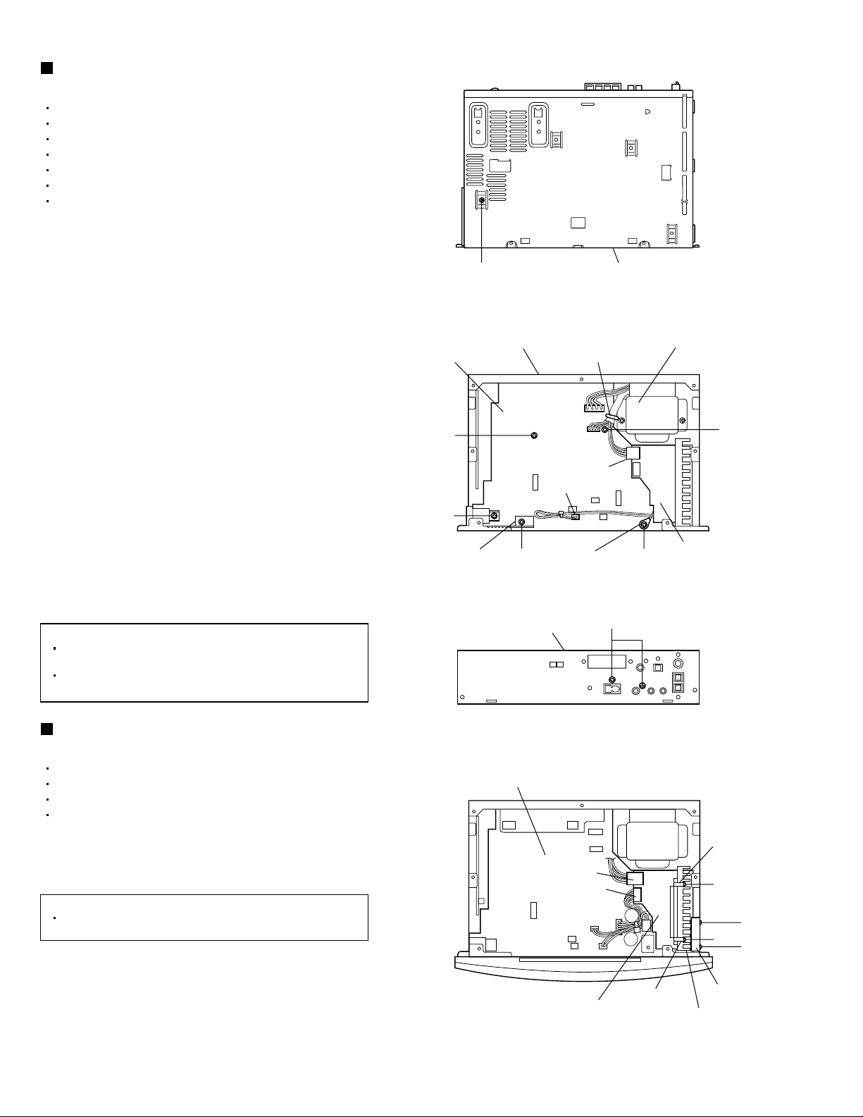
Removing the main board
(See Figs. 10 to 12.)
Remove the top lens.
Remove the bottom panel.
Remove the top panel.
Remove the CD&Video CD mechanism assembly.
Remove the front panel assembly.
Remove the tuner board.
Remove the speaker board.
1.
From the bottom side of the bottom chassis,
remove the screw K attaching the main board.
(See Fig.10.)
2.
Disengage the wire clamp bundling the wire of the
power transformer. (See Fig.11.)
3.
Disconnect the wires from connectors CN181,
CN191 and CN194 on the main board.
(See Fig.11.)
4.
Disconnect the wire from connector CN192 on the
power amplifier board.(See Fig.11.)
5.
Remove the screw L, which retains the main board,
together with the wire holder. (See Fig.11.)
6.
Remove the two screws M, screw M' and screw N
attaching the main board. (See Fig.11.)
7.
Remove the two screws P attaching the main
board and then remove the rear panel. (See
Fig.12.)
K
Main board
M
N
Wire holder
Bottom chassis
Fig.10
Bottom chassis
Wire clamp
CN191
CN194
CN181
LM'
CN192
Earth wire
Power transformer
Power amplifier
board
M
8.
Take out the main board with the power amplifier
board from the bottom chassis.
[Reference] Attaching the main board
When attaching the screw M', attach the earth
wire of the main board at the same time.
When attaching the screw L, also attach the
wire holder together with it.
Removing the power amplifier board
(See Fig. 13.)
Remove the top lens.
Remove the bottom panel.
Remove the top panel.
Remove the CD&Video CD mechanism assembly.
1.2.Disconnect the wires from connectors CN192 and
CN193 on the power amplifier board.
Remove the two screws Q attaching the fan motor.
[Reference]
It is not necessary to remove the wire from
the fan motor.
3.4.Remove the two screws R attaching the power
amplifier board.
Lift the power amplifier board, disengage the two
hooks e from the heat sink of the main board and
take out the power amplifier board.
Rear panel
Main board
Fig.11
P
Fig.12
CN192
CN193
Power amplifier
board
Fig.13
Hook e
Hook e
R
R
Fan motor
Heat sink
Q
Q
1-8
Page 9
Removing the power transformer
(See Fig. 14.)
VS-DT88V
Remove the top lens.
Remove the bottom panel.
Remove the top panel.
Remove the CD&Video CD mechanism assembly.
1.
Disengage the wire clamp and tie band bundling
the wires of the power transformer.
2.
Disconnect the wire from connector CN192 on the
power amplifier board.
3.
Disconnect the wires from connectors CN191 and
CN194 on the main board.
4.
Remove the two screws S and two washers
attaching the power transformer.
[Reference]
After connecting the wires, bundling them
using a wire clamp and tie band.
Main board
Treat the wire from the fan motor.
Fan motor
Tie band
Wire clamp
CN191
CN194
CN192
CN181
Power amplifier board
Fig.14
Power transformer
Washers
S
Fan motor
Removing the fan motor
(See Figs. 14 and 15.)
Remove the top lens.
Remove the bottom panel.
Remove the top panel.
Remove the CD&Video CD mechanism assembly.
Remove the front panel assembly.
1.2.Disconnect the wire from connector CN181 on the
main board. (See Fig.14.)
From the right side of the main body, remove the
two screws Q attaching the fan motor. (See Fig.15.)
[Reference]
After mounting the fan motor, treat the wire
from the fan motor as shown in fig. 14.
Q
Bottom chassis
Fig.15
1-9
Page 10
VS-DT88V
<Front panel assembly section>
Remove the top lens.
Remove the bottom panel.
Remove the top panel.
Remove the CD&Video CD mechanism assembly.
Remove the front panel assembly.
Removing the switch board
(See Fig. 16.)
From the back side of the front panel assembly,
remove the four screws T attaching the switch
board.
Removing the open/close board
(See Figs. 16 and 17.)
1.2.From the back side of the front panel assembly,
remove the two screws U attaching the door motor
assembly.
Remove the screw V attaching the open/close
board of the door motor assembly.
Removing the door motor (See Fig. 16.)
Remove the door motor assembly.
1.
Remove the washers attaching the clutch assembly
and gear 2.
2.
Remove the clutch assembly and Gear 2.
Door motor assembly
U
Clutch assembly
Washer
Gear 2
Front panel assembly
(Back side)
T
Switch board
Front panel assembly
(Back side)
Fig.16
Door motor
W
V
Open/close
board
Door motor assembly
Fig.17
Rod gear assembly
f
3.
Remove the two screws W attaching the door
motor.
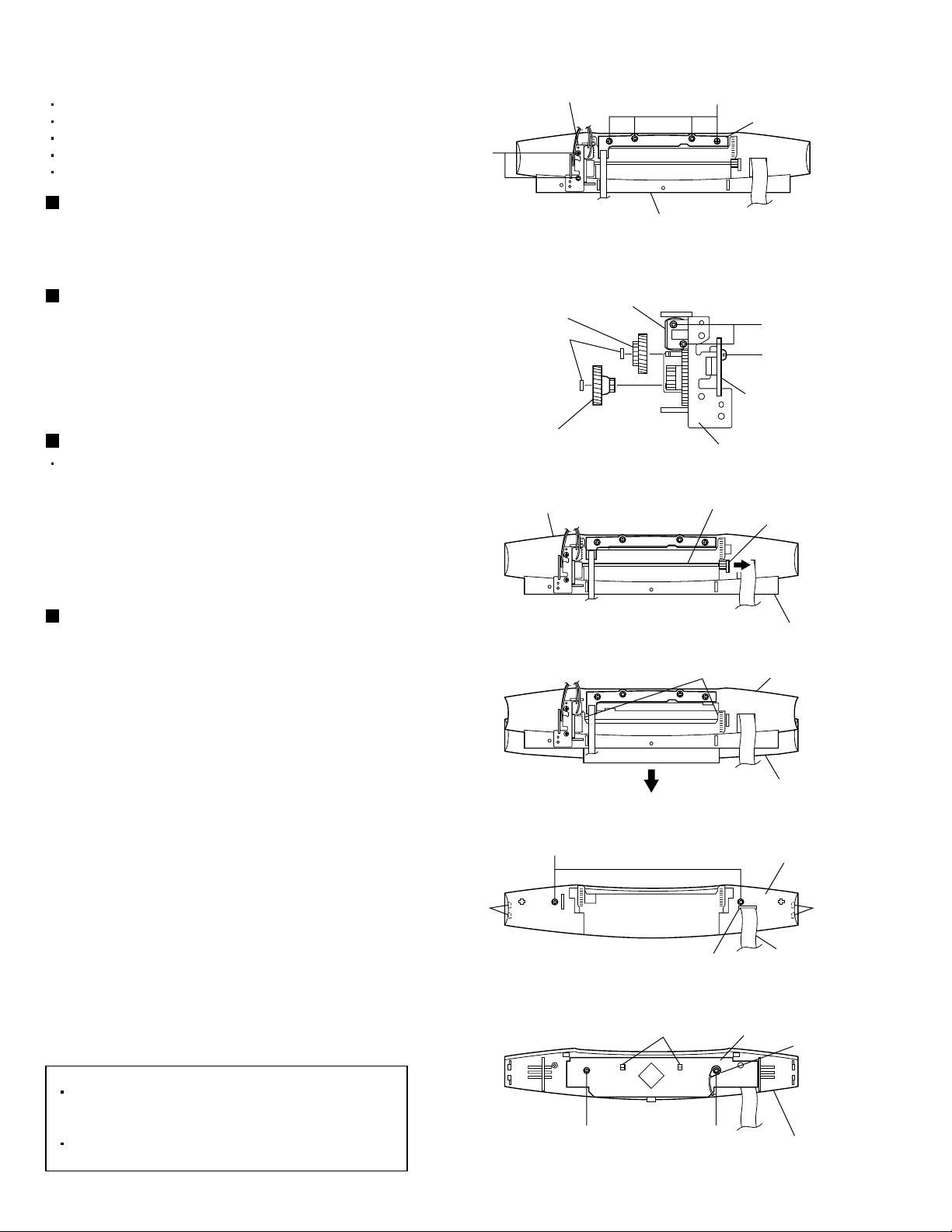
Removing the front board
(See Figs. 18 to 21.)
1.
While widening section f of the front base in the
direction of the arrow, remove the rod gear
assembly. (See Fig.18.)
2.
Slide the moving panel assembly all the way in the
direction of the arrow. (See Fig.18.)
3.
While slightly widening sections g toward the front,
take out the moving panel assembly in the direction
of the arrow. (See Fig.19.)
4.
Remove the two screws X attaching the moving
base of the moving panel assembly. (See Fig.20.)
5.
Disengage the engagement sections h on the
inside of the moving base and at the inside of the
moving panel assembly and remove the moving
base. (See Fig.20.)
6.
Remove the screw Y and screw Y' attaching the
front board. (See Fig.21.)
7.
Disengage the claws i of the moving panel and
remove the front board. (See Fig.21.)
[Reference]
Before attaching the moving base, pass the
card wire of the front board through the hole
on the moving base. (See Fig.20.)
When attaching the screw Y', attach the wire
at the same time.
X
Y
Fig.18
Fig.19
Fig.20
Fig.21
Front base
g
Moving panel assembly
Hole
i
Y'
Front base
Moving base
Front board
Moving panel
hh
Card wire
Wire
1-10
Page 11
VS-DT88V
<CD&Video CD mechanism
assembly section>
Removing the LED board (See Fig. 1.)
From the top side of the CD&Video CD mechanism
assembly, disengage the claw a of the top chassis
attaching the LED board and then remove the LED
board.
Removing the CD&Video CD
mechanism assembly (See Fig. 2.)
From the back side of the CD&Video CD
1.
mechanism assembly, raise the protector in the
direction of arrow.
Remove the three screws A attaching the
2.
CD&Video CD mechanism assembly on the top
chassis and then remove the CD&Video CD
mechanism assembly.
Removing the CD servo board and
video board (See Fig. 3.)
[Caution] Be sure to solder the short land
section b on the flexible wire before
disconnecting the flexible wire from
connector CN601 on the CD servo
board.
If the flexible wire is disconnected
without attaching solder, the pickup
unit may be destroyed by static
electricity.
1.
From the back side of the CD&Video CD
mechanism assembly, attach solder to the short
land section b of the flexible wire that is connected
to the connector CN601 of the CD servo board.
Claw a
A
Protector
LED board
Top chassis
Fig.1
CD&Video CD mechanism assembly
A
Top chassis
Fig.2
2.
Disconnect the flexible wire from connector CN601
on the CD servo board.
3.
Disconnect the card wires from connectors CN611,
CN612, CN691 and CN692 on the CD servo
board.
4.
Remove the two screws B attaching the CD servo
board.
5.
Lift the front edge of the CD servo board slightly
and disengage it from the projection c and then
from the engagement section d.
[Caution] In the assembly, be sure to remove
solder from the short land section b
after connecting the flexible wire.
6.7.From the back side of the CD&Video CD
mechanism assembly, disconnect the card wires
from connectors CN101 and CN102 on the video
board.
Remove the two screws C attaching the video
board and then remove the video board.
Flexible wire
Projection c
Short land section b
CN612
CN601
CN691
CN611
CN692
CD servo board
Engagement section d
CN102
CN101
Video board
B
Fig.3
C
1-11
Page 12

VS-DT88V
Removing the traverse mechanism
assembly (See Fig. 4.)
Remove the CD servo board and video board.
1.
Remove the two screws D attaching the CD servo
board bracket.
2.
Remove the two screws E and O-rings attaching
the traverse mechanism assembly.
3.
Disengage the claw e attaching the traverse
mechanism assembly and then take out the
traverse mechanism assembly.
Removing the pickup unit
(See Figs. 5 and 6.)
Remove the CD servo board and video board.
Remove the traverse mechanism assembly.
Traverse mechanism
assembly
O-ring
F
Claw e
Fig.4
Pickup unit
CD servo board
D
bracket
EE
Section f
O-ring
1.
From the top side of the traverse mechanism
assembly, remove the two screws F attaching the
shaft.
2.
From the traverse mechanism assembly, disengage
the section f of the pickup unit and then remove the
pickup unit with the C.D shaft. (See Fig.5.)
3.
Pull the C.D shaft out of the pickup unit.
(See Fig.6.)
4.
Remove the screw G attaching the rack from the
pickup unit. (See Fig.6.)
5.
Remove the screw H attaching the P.S. spring from
the pickup unit. (See Fig.6.)
F
C.D shaft
Traverse mechanism assembly
Fig.5
C.D shaft
Pickup unit
P.S. spring
H
G
Rack
Fig.6
1-12
Page 13

VS-DT88V
Attaching the pickup unit
(See Figs. 6 to 8.)
[Reference]
Refer to the explanation of "Removing the
pickup unit" on the preceding page.
1.
Attach the P.S. spring and rack to the pickup unit.
(See Fig.6.)
2.
Insert the C.D shaft into the pickup unit.
(See Fig.6.)
3.
Engage the section f of the pickup unit with the
traverse mechanism assembly first, and set the
both ends of the C.D shaft in the grooves g and h.
(See Fig.7.)
4.
After making sure that the section j of the rack is
meshed correctly with the middle gear, attach the
C.D shaft using the two screws F. (See Fig.8.)
Section f
Groove g
Groove h
Fig.7
Section j
F
Removing the traverse mechanism
board (See Fig. 9.)
Remove the CD servo board and video board.
Remove the traverse mechanism assembly
1.
From the back side of the traverse mechanism
assembly, disconnect the spindle motor wires and
feed motor wires that are soldered on the traverse
mechanism board.
2.
Remove the two screws J attaching the traverse
mechanism board.
Removing the feed motor (See Fig. 9.)
Remove the CD servo board and video board.
Remove the traverse mechanism assembly.
1.
From the back side of the traverse mechanism
assembly, disconnect the feed motor wires that are
soldered on the traverse mechanism board.
K
J
Black
Feed motor
Rack
Fig.8
Traverse mechanism assembly
Spindle motor
Red
Traverse
mechanism board
Red
J
Fig.9
2.
Remove the two screws K attaching the feed
motor.
1-13
Page 14

VS-DT88V
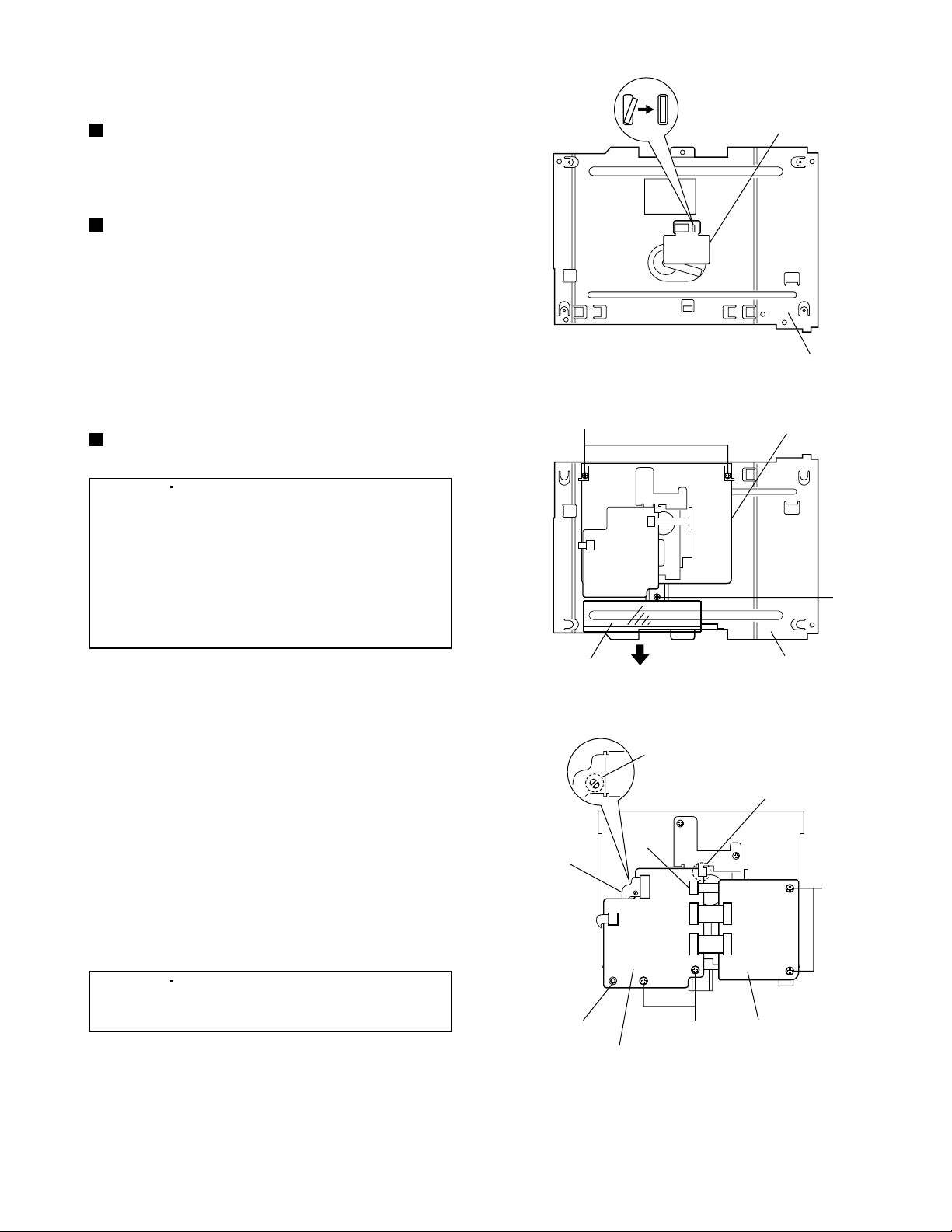
Removing the CD switch board
(See Fig.10.)
Remove the CD&Video CD mechanism assembly.
1.
From the top side of the CD&Video CD mechanism
assembly, remove the screw L attaching the CD
switch board.
2.
Lift the CD switch board slightly and then remove
the wire from connector CN101 on the CD switch
board.
Removing the loading motor assembly
(See Figs.10 to 13.)
Remove the CD&Video CD mechanism assembly.
1.
From the back side of the CD&Video CD
mechanism assembly, disconnect the card wire
from connector CN612 on the CD servo board.
(See Fig.11.)
2.
Remove the screw N attaching the roller holder
assembly. (See Fig.11.)
3.
From the top side of the CD&Video CD mechanism
assembly, remove the two screws M attaching the
clamper base assembly. (See Fig.10.)
CD&Video CD mechanism assembly
L
CN101
M
CD switch board
Fig.10
Card wire
CN612
Clamper base assembly
M
N
4.
Disconnect the wire from connector CN101 on the
CD switch board while lifting the clamper base
assembly slightly and remove the clamper base
assembly. (See Fig.10.)
5.
Remove the three screws P attaching the roller
holder assembly and take out the roller holder
assembly. (See Fig.12.)
6.
Disconnect the wires from connectors CN103 and
CN104 on the loading motor assembly.
(See Fig.13.)
7.
Remove the belt of the loading motor assembly.
(See Fig.13.)
8.
Remove the two screws Q attaching the loading
motor assembly and take out the loading motor
assembly. (See Fig.13.)
CD servo board
P
CN103
Fig.11
P
Roller holder
assembly
Fig.12
CN104
Loading motor assembly
1-14
Q
Q
Belt
Fig.13
Page 15

Flow of functional operation until TOC read
Power ON Play Key
Slider turns REST
SW ON.
Automatic tuning
of TE offset
Laser ON
Detection of disc
Automatic tuning of
Focus offset
VS-DT88V
Check Point
Confirm that the voltage at the pin4
of CN611 is "H"\"L"\"H".
Tracking error waveform at TOC reading
Pin 20 of
IC601(TEOUT)
Approx
1.8V
VREF
Disc states
to rotate
Approx.3sec
Tracking
servo
off states
Automatic measurement
of TE amplitude and
automatic tuning of
TE balance
Tracking
servo
on states
Disc to be
braked to stop
TOC reading
finishes
500mv/div
2ms/div
Fig.1
Automatic measurement of
Focus S-curve amplitude
Disc is rotated
Focus servo ON
(Tracking servo ON)
Automatic measurement of
Tracking error amplitude
Automatic tuning of
Tracking error balance
Automatic tuning of
Focus error balance
Confirm that the Focus error
S-curve signal at the pin 28 of
IC651 is approx.2Vp-p
Confirm that the signal from
pin 24 IC651(R808) is 0V as a
accelerated pulse during
approx.400ms.
Confirm the waveform of
the Tracking error signal
at the pin 20 of IC601 (R604)
(See Fig.1.)
Automatic tuning of
Focus error gain
Automatic tuning of
Tracking error gain
TOC reading
Play a disc
Confirm the eys-pattern
at the lead of ARF.
1-15
Page 16

VS-DT88V
Maintenance of laser pickup
(1) Cleaning the pick up lens
Before you replace the pick up, please try to
clean the lens with a alcohol soaked cotton
swab.
(2) Life of the laser diode
When the life of the laser diode has expired,
the following symptoms will appear.
The level of RF output (EFM output : ampli
tude of eye pattern) will below.
Is the level of
RFOUT under
1.25V 0.22Vp-p?
YES
O.K
NO
Replace it.
Replacement of laser pickup
Turn off the power switch and, disconnect the
power cord from the ac outlet.
Replace the pickup with a normal one.(Refer
to "Removing the pickup unit" on the previous page)
Plug the power cord in, and turn the power on.
At this time, check that the laser emits for
about 3seconds and the objective lens moves
up and down.
Note: Do not observe the laser beam directly.
Play a disc.
Check the eye-pattern at ARF.
Finish.
(3) Semi-fixed resistor on the APC PC board
The semi-fixed resistor on the APC printed circuit board which is attached to the pickup is used to adjust the laser
power. Since this adjustment should be performed to match the characteristics of the whole optical block, do not
touch the semi-fixed resistor.
If the laser power is lower than the specified value, the laser diode is almost worn out, and the laser pickup should
be replaced.
If the semi-fixed resistor is adjusted while the pickup is functioning normally, the laser pickup may be damaged
due to excessive current.
1-16
Page 17

Description of major ICs
MN101C35DKB (IC811) : FL driver microcomputer
1. Terminal layout
100 76
1
75
VS-DT88V
25
26 50
2. Pin function
51
Pin No. Symbol I/O Function
1
2
3
4
5
6,7
8
9
10
11,12
13
14~23
24
25
26
27~30
31
32
33~38
39,40
41
42
43
44~46
47
48~60
61
62~64
65~99
100
NC
FLDATA
FLCLK
NC
FLCS
NC
B5V
OSC2
OSC1
GND
NC
GND
VREF+
NC
FLRST
NCV70
REMCON_HO
NCV70
GND
NCV70
KEYLEDH
KEYLEDV
KEYDIMMER
NC
G1
G2~G14
G15
S1~S35
-VPP
-
Not connect
I/O
FL driver communication data input/output
I
FL driver communication clock input
-
Not connect
I
FL driver communication chip select input
-
Not connect
-
VDD(B5V)
O
8MHz main clock output
I
8MHz main clock input
-
Ground
-
Not connect
-
Ground
-
Reference voltage
-
Not connect
I
FL reset input
-
Not connect
O
Switching signal for receiver part of remote controller
-
Not connect
-
Ground
-
Not connect
-
Horizontal KEY LED control
-
Vertical KEY LED control
-
KEY LED DIMMER control
-
Not connect
-
Not connect
O
Grid signal outputs
-
Not connect
-
Not connect
O
Segment signal outputs
-
VPP
BA15218F (IC102,IC401) : Dual operational amplifier
1. Terminal layout & Block diagram
OUT1
IN1-
IN1+
VEE
1
2
1
3
4
8
Vcc
7
OUT2
6
IN2-
2
5
IN2+
1-17
Page 18

VS-DT88V
MN101C30AEN (IC701) : System control microcomputer
1. Terminal layout
64 49
1
48
16
17 32
2. Pin function
33
Pin No. Symbol I/O Function
1
2
3
4
5
6
7
8
9
10
11
12
13
14
15
16
17
18
19
20
21
22
23
24
25
26
27
28
29
30
31
32
33
34
35
36
37
38
39
40
THERM
KEY1
KEY2
VERSION
GND
VREF+
VDD
OSC2
OSC1
VSS
XI
XO
GND
CDTX
CDRX
FLRST
FLCOM
FLDATA
FLCLK
STBLEDH
RST
STBLEDV
FTU
TUDATA
TUST
TUCK
MPX
REM
GND
SMUTE
AHB
VOLDI
VOLCE
VOLCL
LOMUTE
TREMCONT
H-V
I
Temperature detection, ON/OFF control of FAN_SW signal (pin 57)
I
Key switch input of the main body
I
Key switch input of the main body
I
Switching signal for destination
-
Ground
-
Reference voltage for A/D converter
-
Power supply for microcomputer
O
8MHz main clock output
I
8MHz main clock input
-
Ground for microcomputer
I
32.768kHz sub clock input
O
32.768kHz sub clock output
-
Ground
O
CD(FMU-F2) communication
I
CD(FMU-F2) communication
O
FL reset output
I/O
FL driver communication data input/output
O
FL driver communication chip select output
O
FL driver communication clock output
O
Standby LED for horizontal establishment (POWER_OFF/ON=H)
I
Microcomputer reset input
O
Standby LED for vertical establishment (POWER_OFF/ON=H)
O
Power supply for tuner
I/O
PLL input/output data (Connect to tuner.)
O
PLL strobe output (Connect to tuner.)
O
PLL clock output (Connect to tuner.)
I
Stereo detection (Connect to tuner.), STEREO=L
-
Not connect
-
Not connect
I
Remote controller input
-
Ground
O
Mute signal, MUTE=L
O
Bass boost, ON=L, POWER_OFF=L
O
Data output (Connect to VOLUME_IC.)
O
Enable output (Connect to VOLUME_IC.)
O
Clock output (Connect to VOLUME_IC.)
O
Line out mute signal, MUTE=L
I
Remote controller effective signal for horizontal establishment, L : effective state
-
Connect to ground
I
Detecting signal for horizontal or vertical establishment
1-18
Page 19

VS-DT88V
Pin No. Symbol I/O
41
42
43
44
45
46
47
48
49
50
51
52
53
54
55
56
57
58
50
60
61
62
63
64
CDRST
BLCTL
PSAVE
FCD
POUT
TOPLED1
TOPLED2
STBDIM
DOOR1
DOOR2
+BCTL
BUP
FANSW
MT0
MT1
MTS
VREFLOCK
SAFETYCD
SAFETY
-
-
-
O
-
O
O
O
O
O
O
O
O
O
O
-
Function
Connect to ground
Connect to ground
Connect to ground
CD reset output (Connect to FMU-F2.)
Connect to ground
Not connect
Power save mode ON/OFF signal, SAVE=H
CD power supply ON/OFF
Main power supply ON/OFF
LED color control (Software PWN output)
LED color control (Software PWN output)
I
Dimmer control for STBYLED_H/V
I
Moving panel position detecting signal, CLOSE=L
I
Moving panel position detecting signal, OPEN=L
Unnecessary power supply cut-off signal for outage, Outage=H
I
Outage detecting signal (Backup mode)
Fan motor ON/OFF signal
Panel open (Motor driver)
Panel close (Motor driver)
Panel action speed
Reference voltage for A/D converter (Connect to ground.)
I
Detection signal for panel action load
I
Detecting signal for CD abnormal voltage
I
Detecting signal for abnormal voltage
KIA78S06P (IC702) : Regulator
1. Terminal layout 3. Block diagram
123
2. Pin function
Pin No.
1
2
3
Output
GND
Input
Function
Z1
Q14
Q16
Q1
R9
R10
R11
Q2
Q7
UPC78L05J (IC191) : Three terminal voltage regulator
1. Terminal layout
1 : OUTPUT
2 : GND
3 : INPUT
123
2. Circuit diagram
R13
Q10
R14
R15
D1
Q15
R16
Q11
R17
Q5
Q4
R1
Q1
Q4
R1
Q8
Q3
R4
R2
Q6
Q6
R2
R3
Q2
Q8
R5
C1
R3
Q9
Q3
C1
R9
R6
Q13
Q5
R4
Q9
Q7
Q10
D2
R19
R18
R11
Q12
Q11
Q12
R12
R7
R8
Q14
R10
Q13
R7
R5
R6
INPUT
OUTPUT
GND
3
INPUT
OUTPUT
1
2
GND
1-19
Page 20

VS-DT88V
MN101C30AKK (IC251) : Unit microcomputer
1. Terminal layout
64 49
1
48
16
17 32
2. Pin function
33
Pin No. Symbol I/O Function
1
2
3
4
5
6
7
8
9
10
11
12
13
14
15
16,17
18
19
20
21
22
23
24
25
26
27
28
29
30
31
32
33
34
35 - 48
49
50
51
52
53
54
/SW1
/SW2(P.UP)
/SW3(P.UP)
PCHKCD
PCHKVCD
VREF+
VDD
OSC2
OSC1
VSS
XI
XO
MMOD
M S TAT
KCMD
NC
SUBQ
SQCK
/VCDRST
/CDMRST
NC(O)
UDSASTB
UDSADAT
UDSAACK
NC
BLKCK
NC
FLAG
NC
NC
DSASTB
DSADAT
DSAACK
NC
REST(P.UP)
/DRMUTE
FWD
REV
/PONCD
NC
I
Mechanism SW1 input
I
Mechanism SW2 input
I
Mechanism SW3 input
I
Detection of /PONCD status
I
Detection of /PONMP3 status
-
Reference voltage (Connect to power supply)
-
Power supply
O
X'tal OSC output terminal
I
X'tal OSC input terminal
-
Ground
-
Connect to ground
-
Not use
I
Connect to ground
O
Mechanism status output
I
Command signal input
-
Not use (Connect to ground)
I
Sub-code Q data input
O
Clock input for sub Q reg.
O
VCD reset signal
I
Micom reset
O
Not use (CD LSI supply enable)
I/O
VCD companion chip STB
I/O
VCD companion chip DAT
I/O
VCD companion chip ACK
-
Not use (Connect to ground)
I
Sub-code block clock signal
-
Not use (Connect to ground)
I
Outside clock for sub-code Q register input
-
Not use (Connect to ground)
-
Not use (Connect to ground)
I/O
VCD processor STB
I/O
VCD processor DAT
I/O
VCD processor ACK
-
Not use (Connect to ground)
I
Reset switch input
O
Mute for drive IC
O
Loading (EJECT) output
O
Loading (LOAD) output
O
CD LSI supply enable
-
Not use (Connect to ground)
1-20
Page 21

VS-DT88V
Pin No.
55
56
57
58
59
60
61
62
63
64
Symbol I/O Function
/PONVCD
/LSIRST
S TAT
M DATA
MCLK
MLD
VREF/TLOCK
/FLOCK
SENSE
O
MP3 LSI supply enable
O
CD LSI reset
I
Status input from CD LSI
I/O
CD LSI MDATA (Serial data)
O
CD LSI MCLK (Serial clock)
O
Command load signal O/P
-
Reference voltage (Connect to ground)
I
Tracking servo lock
I
Focus servo lock
I
Sense signal input
LA4905 (IC301) : 2ch BTL power amplifier
1. Terminal layout 2. Block diagram
CVL
C
SWB VL VL
8
9 15 14 12 13 16 7 5 6 18 19 17 22
SW
123
VH
VH
11
10
drive
D
H.L.S.
Switching regulator
block
Standby
SW
ST-BY RF PREGND IN 1 IN 2 ON-TIMEBEEP
C
B
A
Ripple
filter
SW
GND
Amplifier
output
stage
H.L.S. :
Higher
Level signal
selector
+OUT1 +OUT2 NC-OUT1 -OUT 2PG1 PG2
AB D
Nonlinear/output stage
CH 1
Input
amplifier
BEEP
amplifier
C
Power supply/ground
shorting protection circuit
Overvoltage/thermal
protection circuit
CH 2
Input
amplifier
Nonlinear amplifier/output
stage
Pop noise
prevention
circuit
ON MUTE
muting circuit
2314322021
NJM4580D-D (IC101) : Dual operational amplifier
1. Terminal layout & Block diagram
8 7 6 5
B
A
1 2 3 4
1. OUT1
2. IN1-
3. IN1+
4. VEE
5. IN2+
6. IN2-
7. OUT2
8. VCC
1-21
Page 22

VS-DT88V
ES3880FL (IC101) : VCD processor
1. Terminal layout
80 ~ 51
100 ~ 81
1 ~ 30
2. Block diagram
Processor
Interface
/LCS3, /LCS[1:0]
31 ~ 50
Serial
Audio
Interface
SEL_PLL[1:0]
TDM
Interface
LA[17:0]
LD[7:0]
/LWR
/LOE
ACLK
ATCLK
AIN
AOUT
ARFS
ATFS
ARCLK
TDMCLK
TDMDR
TDMFS
RISC
Processor
Serial Audio
Interface
TDM
Interface
3. Pin function
Pin No. Symbol I/O Function
1
2
3
4 - 12
13 - 28
29
30
31
32 - 39
40
41
42
VDD3
/RAS
/DWE
MA0 - 8
DBUS0 - 15
/RESET
GND
VDD3
YUV0 - 7
VSYNC
HSYNC
CPUCLK
3.3V power supply
Row address strobe
O
DRAM write enable
O
DRAM multiplexed row and column address bus
O
DRAM data bus
I/O
System reset
I
Ground
-
3.3V power supply
YUV[7:0] 8-bit video data bus
O
Vertical sync
I/O
Horizontal sync
I/O
RISC and system clock input.
I
CPUCLK is used only if SEL_PLL[1:0] = 00 to bypass PLL.
43
44
45 - 49
50
51
52
53
54
55 - 62
63
64
65
66
67
68 - 79
80
81
82 - 87
88
PCLK2X
PCLK
AUX0 - 4
GND
VDD3
AUX6
AUX5
AUX7
LD0 - 7
/LWR
/LOE
/LCS3
/LCS1
/LCS0
LA0 - 11
GND
VCC
LA12 - 17
ACLK
Doubled 54MHz pixel clock
I/O
27MHz pixel clock
I/O
Auxiliary control pins 4:0, AUX0 and AUX1 are open collectors.
I/O
Ground
-
3.3V power supply
Auxiliary control pins 6
I/O
Auxiliary control pins 5
I/O
Auxiliary control pins 7
I/O
RISC interface data bus
I/O
RISC interface write enable (Not connect)
O
RISC interface output enable
O
RISC interface chip select
O
RISC interface chip select
O
RISC interface chip select
O
RISC interface address bus
O
Ground
-
5.0V power supply
RISC interface address bus
O
Master clock for external audio DAC
I/O
Huffman
Decoder
64x32 ROM
32x32 SRAM
Registers
DRAM DMA
Controller
DRAM Interface
2Kx32 ROM
512x32 SRAM
MPEG
Processor
Video Output
On Screen
Display
/RAS
MA[9:0]
DBUS[15:0]
/DOE
/DWE
/CAS
AUX[7:0]
YUV[7:0]
PCLK2X
PCLK
VSYNC
HSYNC
CPUCLK
/RESET
DRAM
AUX
Screen
Display
Misc.
1-22
Page 23

Pin No. Symbol I/O Function
89
AOUT
SELPLL0
Audio interface serial data output when selected.
O
System and DSCK output clock frequency selection at reset time. The matrix below
I
lists the available clock frequencies and their respective PLL bit settings.
SELPLL1 SELPLL0 DCLK
0 0 Bypass PLL (input mode)
0 1 54MHz (output mode) Default
1 0 67.5MHz (output mode)
1 1 81.0MHz (output mode)
VS-DT88V
90
91
92
93
94
95
96
97
98
99
100
ATCLK
ATFS
SELPLL1
DA9
/DOE
AIN
ARCLK
ARFS
TDMCLK
TDMDR
TDMFS
/CAS
GND
Audio transmit bit clock
I/O
Audio transmit frame sync
O
Refer to the description and matrix for SEL_PLL0 pin 89.
I
DRAM multiplexed row and column address line 9
O
DRAM output enable
O
Audio serial data input
I
Audio receive bit clock
I
Audio receive frame sync
I
TDM serial clock
I
TDM serial data receive
I
TDM frame sync
I
DRAM column address strobe
O
Ground
-
TC7S08F (IC106) : 2-inputs AND gate
1. Terminal layout
1
IN B 54Vcc
IN A
2
GND
3
OUT Y
2. Truth table
INPUTS OUTPUT
A
B
L
L
L
H
H
L
H
H
Y
L
L
L
H
TC7W08FU (IC107) : Dual 2-inputs AND gate
1. Terminal layout
11A
1B
2
2Y
3
GND 4
8 Vcc
1Y
7
2B
6
2A5
2. Truth table
INPUTS OUTPUT
A
L
L
H
H
B
L
H
L
H
Y
L
L
L
H
1-23
Page 24

VS-DT88V
ES3883F (IC104) : VCD companion chip
1. Terminal layout
80 ~ 51
100 ~ 81
1 ~ 30
31 ~ 50
2. Pin function
Pin No. Symbol I/O Function
1,2
3
4,5
6
7
8
9
10
11
12
GND
NC
VCC
DSCC
AUX00
DSCD0
AUX01
DSCS
AUX02
DCLK
EXTCLK
Ground
No connect
Voltage supply, 5V
Clock for programming to access internal registers
I
Servo forward or general-purpose I/O (Not connect)
I/O
Data for programming to access internal registers
I/O
Servo reverse or general-purpose I/O (Not connect)
I/O
Strobe for programming to access internal registers
I
Servo LDON or general-purpose I/O (Not connect)
I/O
DCLK is the MPEG decoder clock.
O
EXT_CLK is the external clock.
I
EXT_CLK is an input during bypass PLL mode.
13
14
15
16
17
18
19
20
21
22
23
/RST
AUX07/NFD_DI
MUTE
VCC
MCLK
AUX08/NFD_CLK
TWS
SPLLOUT
AUX09/SQSO
TSD
TBCK
RWS
SPLL1
Video reset (active-low)
I
Servo BRKM/sense or general-purpose I/O / VFD_DI (Not connect)
I/O
Audio mute (Not connect)
O
Voltage supply, 5V
Audio master clock
I
Servo mute/open or general-purpose I/O / VFD_CLK (Not connect)
I/O
TWS is the transmit audio frame sync.
I
SPLL_OUT is the select PLL output.
O
Servo SQSO or general-purpose I/O (Not connect)
I/O
Transmit audio data input
I
Transmit audio bit clock
I
RWS is the receive audio frame sync.
O
SPLL[1:0] select the PLL clock frequency for the DCLK output.
I
SPLL1 SPLL0 DCLK
0 0 Bypass PLL (input mode)
0 1 27MHz (output mode)
1 0 32.4MHz (output mode)
1 1 40.5MHz (output mode)
1-24
24
25,26
27,28
29 - 31
32
33
34
/RSTOUT
GND
NC
GND
VCC
RSD
SPLL0
AUX10/SQCK
Reset output (active-low)
O
Ground
No connect
Ground
Voltage supply, 5V
RSD is the receive audio data input.
O
SPLL0 and SPLL1 select the PLL clock frequency for the DCLK
I
output. Refer to the table in the definition for pin 23.
Servo SQCK or general-purpose I/O (Not connect)
I/O
Page 25

Pin No. Symbol I/O Function
35
36
37
38
39
40
41
42
43
44
45,46
47,48
49
50
51
52
53
54
55
56,57
58
59,60
61
62,63
64
65
66
67
68
69
70
71
72
73
74
75
76
77
78
79
80
81
82
AUX11/IRQ
AUX12/C2PO
RBCK
SERIN
AUX13/SP
AUX14/SOSI
AUX15/IR
AGND
VREFM
VREFP
AVDD
AOR+,AOR-
AOL-,AOL+
MIC1
MIC2
AGND
VREF
VCM
RSET
COMP
VGND
CDAC
VVID
YDAC
VGND
VDAC
PLLCAP
VDD
AUX06/VFD_DO
AUX05
AUX04
AUX03
XOUT
GND
VDD
XIN
GND
NC
GND
VCC
PCK
PCK2
DSCD7
/HSYNC
ES3880 IRQ or interrupt output or general-purpose I/O (Not connect)
I/O
CD C2PO or interrupt input or general-purpose I/O (Not connect)
I/O
RBCK is the receive audio bit clock.
O
SER_IN is the serial input DSC mode:
I
0 = Parallel DSC mode
1 = Serial DSC mode
Serial interrupt/CD-mute or general-purpose I/O (Not connect)
I/O
Servo SCOR (SOSI), interrupt input, or general-purpose I/O (Not connect)
I/O
Interrupt input or general-purpose I/O (Not connect)
I/O
Audio analog ground
ADC common mode reference (CMR) buffer output. CMR is approximately
I
2.25V. Bypass to analog ground with 47uF electrolytic in parallel with 0.1uF.
DAC and ADC maximum reference. Bypass to video CMR (VCMR) with 10uF
I
in parallel with 0.1uF.
Analog VCC, 5V
I
Right channel output
O
Left channel output
O
Microphone input 1
I
Microphone input 2 (Not connect)
I
Audio analog ground
Internal resister divider generates CMR voltage.
I
Bypass to analog ground with 0.1uF.
DAC and ADC minimum reference.
I
Bypass to VCMR with 10uF in parallel with 0.1uF.
Full-scale DAC current adjustment
I
Compensation pin
I
Video analog ground
Modulated chrominance output
O
Video VCC, 5V
Y luminance data bus for screen video port
O
Video analog ground
Composite video output
O
Audio CAP
I
Voltage supply, 5V
Servo XLAT or general-purpose I/O / VFD_DO (Not connect)
I/O
Servo data or general-purpose I/O (Not connect)
I/O
Servo CCW/close or general-purpose I/O (Not connect)
I/O
Servo CW/limit or general-purpose I/O (Not connect)
I/O
Crystal output
O
Ground
Voltage supply, 5V
27MHz crystal input
I
Ground
No connect
Ground
Voltage supply, 5V
-
13.5MHz pixel clock
I/O
27MHz(2 times pixel clock)
I/O
Data for programming to access internal registers
I/O
Horizontal sync (active-low)
O
VS-DT88V
1-25
Page 26

VS-DT88V
Pin No. Symbol I/O Function
83
84
85
86~89
90
91
92
93
94
95
96
97
98
99
100
DSCD6
/VSYNC
DSCD5
YUV7~4
VCC
GND
YUV3
DSCD4
YUV2
DSCD3
YUV1
DSCD2
YUV0
DSCD1
GND
Data for programming to access internal registers
I/O
Vertical sync (active-low)
O
Data for programming to access internal registers
I/O
YUV data bus for screen video port
I
Voltage supply, 5V
Ground
YUV data bus for screen video port
I
Data for programming to access internal registers
I/O
YUV data bus for screen video port
I
Data for programming to access internal registers
I/O
YUV data bus for screen video port
I
Data for programming to access internal registers
I/O
YUV data bus for screen video port
I
Data for programming to access internal registers
I/O
Ground
-
AT27C020-70JCU2 (IC102) : 2M-bit OTP EPROM
1. Terminal layout
LA12
LA15
LA16
VPP
VCC
/PGM
LA17
432
1
LD2
GND
LD3
323130
LD4
LD5
29
28
27
26
25
24
23
22
21
LD6
LA14
LA13
LA8
LA9
LA11
/LOE
LA10
/LROMCE
LD7
LA7
LA6
LA5
LA4
LA3
LA2
LA1
LA0
LD0
5
6
7
8
9
10
11
12
13
14151617181920
LD1
3. Pin function
Pin No. Symbol I/O Function
1
VPP
2 - 12
13 - 15
17 - 21
25 - 30
LA16, LA15, LA12, LA7 - LA0
LD0 - LD2
16
GND
LD3 - LD7
22
/LROMCE
23
LA10
24
/LOE
LA11, LA9, LA8, LA13, LA14, LA17
31
/PGM
32
VCC
2. Block diagram
VCC
GND
VPP
/LOE
/LROMCE
/PGM
LA0 - LA17
ADDRESS
INPUTS
I
O
-
O
I
I
I
I
I
-
PROGRAM LOGIC
Power supply terminal
Address inputs
Data outputs
Ground terminal
Data outputs
Chip enable terminal
Address input
Output enable terminal
Address inputs
Program strobe
Power supply terminal
/LOE, /LROMCE
AND
Y DECODER
X DECODER
DATA OUTPUTS
LD0 - LD7
OUTPUT
BUFFERS
Y-GATING
CELL MATRIX
IDENTIFICATION
1-26
Page 27

AN22000A (IC601) : RF & Servo amplifier
1. Terminal layout 2. Block diagram
3TOUT
CEA
9 10 15 22 23 21 20 19 18 2 1
14
OFTR 3TENV
13
12
BDO
11
8
AGC
7
6
5
4
NRFDET
RF_EQ
10
11
12
13
14
15
16
1
2
3
4
5
6
7
8
9
32
31
30
29
28
27
26
25
24
23
22
21
20
19
18
17
OFTR
COFTR
BDO
CBDO
ARF
CAGC
RF IN
RF OUT
RFN
FEN
FEOUT/RFDET
SUBT SUBT
BCA
GCA
TEN
BCA
GCA
BCA
GCA
AMPAMPAMP
VS-DT88V
VDET
TEBPFTEOUT
VDET
BCA
GCA
AMP
PDLD
3
VCC
16
GND
FBAL
25
26
TBAL
GCTRL
24
3. Pin function
A C B D PDE PDF VREF
Pin No. Symbol Function
1
2
3
4
5
6
7
8
9
10
11
12
13
14
15
16
17
18
19
20
21
22
23
24
25
26
27
28
29
30
31
32
PD
LD
VCC
RFN
RF OUT
RF IN
CAGC
ARF
CEA
3TOUT
CBDO
BDO
COFTR
OFTR
/RFDET
GND
VREF
VDET
TEBPF
TEOUT
TEN
FEN
FEOUT
GCTRL
FBAL
TBAL
PDE
PDF
D
B
C
A
APC Amp. Input terminal
APC Amp.Output terminal
Power supply terminal
RF addition Amp.Reversing input terminal
RF addition Amp.Output terminal
AGC input terminal
Terminal of connection of capacity of AGC loop filter.
AGC output terminal
Capacity connection terminal for HPF-Amp.
3TENV output terminal
Capacity connection terminal for RF shade side envelope detection
BDO output terminal
Capacity connection terminal for RF discernment side envelope detection
OFTR output terminal
RFDET output terminal (Negative logic)
Earth terminal
VREF output terminal
VDET output terminal
VDET input terminal
TE Amp. output terminal
TE Amp. reversing input terminal
FE Amp. reversing input terminal
FE Amp. output terminal
Terminal GCTL & APC
FBAL control terminal
TBAL control terminal
Tracking signal input terminal 1
Tracking signal input terminal 2
Focus signal input terminal 4
Focus signal input terminal 2
Focus signal input terminal 3
Focus signal input terminal 1
2729303132
28
17
1-27
Page 28

VS-DT88V
MN6627482WA (IC651) : Digital servo & Digital signal processor
1. Terminal layout
21
20 1
80
40
41 60
2. Pin function
61
Pin No. Symbol I/O Function
1
2
3
4
5
6
7
8
9
10
11
12
13
14
15
16
17
18
19
20
21
22
23
24
25
26
27
28
29
30
31
32
33
34
35
36
37
38
39
40
BCLK
LRCK
SRDATA
DVDD1
DVSS1
TX
MCLK
MDATA
MLD
SENSE
/FLOCK
/TLOCK
BLKCK
SQCK
SUBQ
/DMUTE
STAT
DSP_RST
SMCK
PMCK
TRV
TVD
PC
ECM
ECS
KICK
TRD
FOD
VREF
FBAL
TBAL
FE
TE
RFENV
VDET
OFT
TRCRS
/RFDET
BDO
LDON
O
Bit clock output for SRDATA
O
LR signal separation output
O
Serial data output
-
Power supply for digital circuit
-
GND for digital circuit
O
Digital audio interface output
I
Micro computer command clock signal input
I
Micro computer command data input
I
Micro computer command load signal input (L:Load)
O
Sense signal output
O
Focus lock signal output (L:Focus lock)
O
Tracking lock signal output (L:Tracking lock)
O
Sub code block signal output
I
External clock input for sub code Q register input
O
Sub code Q data output
I
Muting input (H:Mute)
O
Status signal input
I
Reset signal input (L:Reset)
-
Not use
-
Not use
O
Traverse enforced output
O
Traverse drive output
-
Not use
O
Spindle motor drive signal (Enforced mode output)
O
Spindle motor drive signal (Servo error signal output)
O
Kick pulse output
O
Tracking drive output
O
Focus drive output
I
Reference voltage for D/A output block
O
Focus balance adjust signal output
O
Tracking balance adjust signal output
I
Focus error signal input (Analog input)
I
Tracking error signal input (Analog input)
I
RF envelope signal input (analog input)
I
Connect to GND
I
Off track signal input (H:Off track)
I
Track cross signal input
I
RF detect signal input (L:Detect)
I
Drop out signal input (H:Drop out)
O
Laser ON signal output (H:ON)
1-28
Page 29

Pin No. Symbol I/O Function
41
42
43
44
45
46
47
48
49
50
51
52
53
54
55
56
57
58
59
60
61
62
63
64
65
66
67
68
69
70
71
72
73
74
75
76
77
78
79
80
PLLF2
TOFS
WVEL
ARF
IREF
DRF
DSLF
PLLF
VCOF
AVDD2
AVSS2
XCLK
DSLB
VCOF2
SUBC
SBCK
VSS
X1
X2
VDD
BYTCK
GIO1
GIO2
IPFLAG
FLAG
CLVS
CRC
DEMPH
RESY
IOSEL
/TEST
AVDD1
OUTL
AVSS1
OUTR
RSEL
CSEL
PSEL
MSEL
SSEL
-
Not use
-
Not use
-
Not use
I
RF signal input
I
Reference current input
I
Bias pin for DSL (Not connect)
I/O
Loop filter pin for DSL
I/O
Loop filter pin for PLL
I/O
Loop filter pin for VCO
-
Power supply for analog circuit
-
GND for analog circuit
-
Not use
O
DSL balance output
I/O
Loop filter pin for digital servo VCO
-
Not use
-
Not use (Connect to ground)
-
GND for crystal oscillation circuit
I
Input for crystal oscillation circuit (f=16.9344MHz)
O
Output for crystal oscillation circuit (f=16.9344MHz)
-
Power supply for crystal oscillation circuit
-
Not use
O
Laser ON signal output (H : ON)
O
Gain control output (H : CD-RW) (Not connect)
-
Not use
O
Flag signal output
-
Not use
-
Not use
-
Not use
-
Not use
I
Mode select pin, connect to ground
I
Test pin, connect to DVDD1 (H fix)
-
Power supply for analog circuit
O
L-channel audio output (Not connect)
-
GND for analog circuit
O
R-channel audio output (Not connect)
-
Not use, connect to DVDD1 (H fix)
-
Connect to ground
I
IOSEL=H , Test pin, not connect
I
IOSEL=H , SMCK output , Frequency select pin, not connect
I
IOSEL=H , SMCK output , SUBQ output mode select pin, not connect
VS-DT88V
LB1641 (IC108) : DC motor driver
1. Terminal layout
1
2 3 4 5 6 7 8 9 10
P1
VZ
IN1
GND
OUT1
IN2
VCC1
VCC2P2OUT2
2. Pin function
Input Output
IN1
0
1
0
1
IN2
0
0
1
1
OUT1
0
1
0
0
OUT2
0
0
1
0
Mode
Brake
Clockwise
Counterclockwise
Brake
1-29
Page 30

VS-DT88V
GLT44016-35J4 (IC103) : 4M-bit DRAM
1. Terminal layout
2. Pin function
VCC
D0
D1
D2
D3
NC
D4
D5
D6
D7
NC
NC
WE
RAS
NC
A0
A1
A2
A3
VCC
1
2
3
4
5
6
7
8
9
10
11
12
13
14
15
16
17
18
19
20
40
GND
39
D15
38
D14
37
D13
36
D12
35
NC
34
D11
33
D10
32
D9
31
D8
30
NC
29
CASL
28
CASH
27
OE
26
A8
25
A7
24
A6
23
A5
22
A4
21
GND
Pin No. Symbol I/O Function
Power supply terminal
1
2 - 5
6
7 - 10
11,12
13
14
15
16 -19
20
21
22 - 26
27
28
29
30
31 - 34
35
36 - 39
40
VCC
D0 - D3
NC
D4 - D7
NC
WE
RAS
NC
A0 - A3
VCC
GND
A4 - A8
OE
CASH
CASL
NC
D8 - D11
NC
D12 - D15
GND
Data inputs/outputs
I/O
Not used
Data inputs/outputs
I/O
Not used
Write enable terminal
I
Row address strobe terminal
I
Not used
Address inputs
I
Power supply terminal
Ground terminal
Address inputs
I
Output enable terminal
I
Upper column address strobe terminal
I
Lower column address strobe terminal
I
Not used
Data inputs/outputs
I/O
Not used
Data inputs/outputs
I/O
Ground terminal
-
GP1FA550TZ (J3601) : Fiber optic transmitter/Receiver
1. Terminal layout 2. Block diagram
LED
Drive
IC
VIN
VCC
GND
RPM6938-V4 (IC801,IC812) : Remote control receiver
1. Block diagram
3
1
2
VDD
OUT
GND
I/V
conversion
PD
magnetic shield
AMP
BPF
for
trimming circuit
AGC
Detector
Vcc
Comp
22k
ohm
1-30
Page 31

LA1838 (IC1) : FM AM IF amplifier & Detector, FM MPX decoder
1. Terminal layout & Block diagram
VS-DT88V
30
ALC
BUFF
FM
S-METER
FM IF
1
29
AM
OSC
S-CLRVE
PM
DET
2
REG
SD
COMP
27
28
AM
MIXFMRF.AMP
AM IF DET
AM/FM
IF-BUFF
4
3
26
AGC
AM
S-METER
GND
25
24
TUNING
DRIVE
5
STEREO
DRIVE
6
7
22
23
VCC
89
P-DET
384KHz
21
DECODER
ANIT-BIRDIE
VCO
10
2. Pin function
Pin No. Symbol I/O Function
This is an input terminal of FM IF signal.
1
2
3
4
5
6
7
8
9
10
11
12
13
14
15
16
17
18
19
20
21
22
23
24
25
26
27
28
29
30
FM IN
AM MIX
FM IF
AM IF
GND
TUNED
STEREO
VCC
FM DET
AM SD
FM VSM
AM VSM
MUTE/IFOUT
FM/AM
MONO/ST
LOUT
ROUT
LIN
RIN
RO
LO
MPX IN
FM OUT
AM DET
AM AGC
AFC
AM RF
REG
AM OSC
OSC BUFFER
I
This is an out put terminal for AM mixer.
O
Bypass of FM IF
I
Input of AM IF Signal.
I
This is the device ground terminal.
When the set is tuning, this terminal becomes "L".
O
Stereo indicator output. Stereo "L", Mono: "H"
O
This is the power supply terminal.
FM detect transformer.
This is a terminal of AM ceramic filter.
Adjust FM SD sensitivity.
O
Adjust AM SD sensitivity.
O
When the signal of IF REQ of IC2(LC72136N) appear, the signal of FM/AM IF output.
I/O
Muting control input.
Change over the FM/AM input. "H" :FM, "L" : AM
I
Stereo : "H", Mono: "L"
O
Left channel signal output.
O
Right channel signal output.
O
Input terminal of the Left channel post AMP.
I
Input terminal of the Right channel post AMP.
I
Mpx Right channel signal output.
O
Mpx Left channel signal output.
O
Mpx input terminal
I
FM detection output.
O
AM detection output.
O
This is an AGC voltage input terminal for AM.
I
This is an output terminal of voltage for FM-AFC.
AM RF signal input.
I
Register value between pin 26 and pin28 besides the frequency width of the input signal.
O
This is a terminal of AM Local oscillation circuit.
AM Local oscillation Signal output.
O
20
STEREO
5N
SW
FF
38k
11
19
MUTE
FF
19k
/
2
12 13
18
FF
19k
17 16
/LS
14
PILOT
DET
15
1-31
Page 32

VS-DT88V
LC72136N (IC2) : PLL frequency synthesizer
1. Terminal layout
2. Block diagram
FM
CE
DI
CK
DO
LW
(MW)
SDIN
1
2
3
4
5
6
7
8
9
10
11
22
21
20
19
18
17
16
15
14
13
12
XIN
VSS
LPFout
LPFin
PD
VDD
FMOSC
AMOSC
IF REQ
FM/AMIF
16
15
17
22
21
1
1/2
3
4
5
6
C2B
I/F
Power
on
Reset
Reference
Swallow Counter
1/16,1/17 4bit
Programmable
Data Shift Register & Latch
721113
XOUT
ST/MONO
AM/FM
3. Pin function
Pin No. Symbol I/O Function
1
2
3
4
5
6
7
8
9
10
11
12
13
14
15
16
17
18
XOUT
FM
CE
DI
CK
DO
ST/MONO
AM/FM
LW
(MW)
SDIN
FM/AM IF
IF REQ
AMOSC
FMOSC
VDD
PD
I
X'tal oscillator connect (75kHz)
O
LOW:FM mode
I
Chip enable, When data output/input for 4pin(input) and 6pin(output): H
I
Input for receive the serial data from controller
I
Sync signal input use
O
Data output for Controller, Output port
O
Stereo:"H", Mono:"L"
O
Open state after the power on reset
I/O
Input/output port (Not use)
I/O
Input/output port (Not use)
I/O
Data input/output
I
IF counter signal input
O
IF signal output
-
Not use
I
AM Local OSC signal output
I
FM Local OSC signal input
-
Power supply(VDD=4.5-5.5V), When power ON:Reset circuit move
O
PLL charge pump output(H: Local OSC frequency Height than Reference
frequency. L: Low Agreement: Height impedance)
19
20
21
22
LPFin
LPFout
VSS
XIN
I
Input for active low pass filter of PLL
O
Output for active low pass filter of PLL
-
Connected to GND
I
X'tal oscillator connect (75KHz)
Driver
12bit
Drivers
8
Phase
Detector
Charge Pump
Unlock
Detector
Universal
Counter
18
19
20
12
1-32
Page 33

LA6575H (IC801) : Focus & Spindle & Feed & Tracking & Loading BTL driver
1. Terminal layout 2. Block diagram
VS-DT88V
1
2
3
4
5
6
7
29
8
9
10
11
12
13
14
28
27
26
25
24
23
22
30
21
20
19
18
17
16
15
REV
FWD
28 27 26 25 24 23 22 30 21 20 19 18 17 16 15
Input
MUTE is as follows:
High: Output ON
Low : Output OFF
Thermal
shutdown
Output
control
CH5 CH4
CH5
POWER
1234567 29 8 9 1011121314
VO5-
VCC2
3. Pin function
Pin No. Symbol Function
1
2
3
4
5
6
7
8
9
10
11
12
13
14
VCC2
VO5VO5+
VO4+
VO4VO3+
VO3VO2+
VO2VO1+
VO1VCC1
VIN1
VIN1G
Power supply for CH3/CH4/CH5
Loading output (-)
Loading output (+)
Tracking output (+)
Tracking output (-)
Focus output (+)
Focus output (-)
Spindle output (+)
Spindle output (-)
Traverse output (+)
Traverse output (-)
Power supply for CH1/CH2
Not use
Traverse drive input
S-GND
MUTE
MUTE
Level
shift
VO5+
VO4+
VIN4
22k 11k
VO4-
VIN4G
Signal
system
power
Level
shift
CH3
VO3+
VCC-S
VO3-
GNDGND
VREF-IN
REG-OUT
5VREG
(External PNP_Tr)
Level
shift
CH2
VO2-
VO2+
Pin No. Symbol Function
15
16
17
18
19
20
21
22
23
24
25
26
27
28
VIN2
VIN2G
VIN3
VIN3G
REG-IN
REG-OUT
VREF-IN
VCC-S
VIN4G
VIN4
MUTE
S-GND
FWD
REV
Not use
Spindle drive input
Not use
Focus drive input
Connect to power supply
Not use
Reference voltage input terminal
Signal system power
Tracking drive input
Not use
Mute for CH1/CH2/CH3/CH4
Signal system ground
Loading input (EJECT)
Loading input (LOAD)
REG-IN
VIN3G
22k
Level
shift
CH1
VO1-
VO1+
11k
22k
11k
CH1- 4
POWER
VIN3
22k
VCC1
VIN2G
VIN2
11k
VIN1
VIN1G
1-33
Page 34

VS-DT88V
LC75342M (IC501) : E. volume
1. Terminal layout
1
DATA
2
CE
3
VSS
4
TEST
5
ROUT
6
RBASS2
7
RBASS1
8
RTRE
9
RIN
10
RSELO
11
R4
12
R3
13
R2
14
R1
15
NC
3. Pin function
Pin No.
Symbol Function
1
DATA
2
3
4
5
6
7
8
9
10
11
12
13
14
15
16
CE
VSS
TEST
ROUT
RBASS2
RBASS1
RTRE
RIN
RSELO
R4
R3
R2
R1
NC
NC
2. Block diagram
RSELO RIN RTRE RBASS1 RBASS2 ROUT
30
29
28
27
26
25
24
23
22
21
20
19
18
17
16
CLOCK
VDD
VREF
NC
LOUT
LBASS2
LBASS1
LTRE
LIN
LSELO
L4
L3
L2
L1
NC
NC
NC
11
R4
12
R3
13
R2
14
R1
15
16
17
L1
18
L2
19
L3
20
L4
10
Serial data and clock input for IC
control
Chip enable
Connect to GND
Electric volume connection for test
Volume control and equalizer input
Connection for resistor and capacitor
that from the bass band filter
Connection for capacitor that from
the treble band filter
Volume control and equalizer input
Input selector output
Input signal connections
Input signal connections
Input signal connections, not use
Input signal connections
Not use
Not use
9 8 7 6 5
CONTROL
CIRCUIT
LOGIC
CIRCUIT
CONTROL
CIRCUIT
Pin No.
17
18
19
20
21
22
23
Symbol Function
L1
L2
L3
L4
LSELO
LIN
LTRE
LVref
CCB
INTERFACE
RVref
LOUTLBASS2LBASS1LTRELINLSELO
Input signal connections
Input signal connections, not use
Input signal connections
Input signal connections
Input selector output
Volume control and equalizer input
Connection for capacitor that from
the treble band filter
24
25
26
27
28
LBASS1
LBASS2
LOUT
VREF
Connection for resistor and capacitor
that from the bass band filter
Volume control and equalizer input
NC
Not use
Connection to the 0.5X VDD voltage
generator circuit used as the analog
signal ground
29
30
VDD
CLOCK
Power supply
Serial data and clock input for IC
control
4
TEST
3
VSS
2
CE
1
DATA
30
CLOCK
29
VDD
28
VREF
27
NC
262524232221
1-34
Page 35

< MEMO >
VS-DT88V
1-35
Page 36

VS-DT88V
VICTOR COMPANY OF JAPAN, LIMITED
AUDIO & COMMUNICATION BUSINESS DIVISION
PERSONAL & MOBILE NETWORK BUSINESS UNIT. 10-1,1Chome,Ohwatari-machi,maebashi-city,371-8543,Japan
No.21179
200209
 Loading...