

Page 1
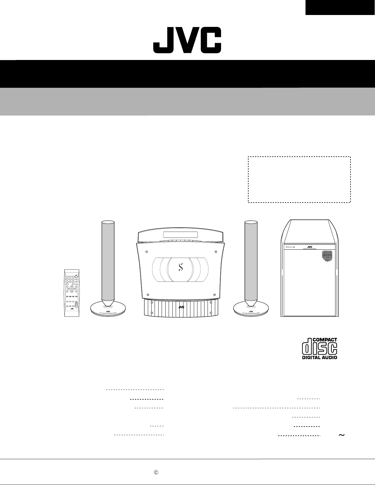
SERVICE MANUAL
COMPACT COMPONENT SYSTEM
VS-DT2000
Area suffix
J ----------------------------- U.S.A.
C -------------------------- Canada
VS-DT2000
STANDBY/ON
123
PLAY MODE
4
6
5
REPEAT
9
8
7
FM MODE
10
+
10
TREBLEBASS
SET
CANCEL
MD/AUX
SLEEPDIMMERDISPLAYFM/AM
CLOCK
OPEN/
COLOR
/TIMER
CLOSE
VOLUME
RM-SVSDT
2000J REMOTE CONTROL
Contents
Safety precautions
Preventing static electricity
Important for laser products
Importance administering point
on the safety
Disassembly method
COMPACT COMPONENT SYSTEM
CA-VSDT2000RSP-VSDT2000 SP-VSDT2000 SP-PW2000
1-2
1-3
1-4
1-5
1-7
Flow of functional operation
until TOC read
Error code
Maintenance of laser pickup
Replacement of laser pickup
Description of major ICs
1-20
1-21
1-22
1-22
1-23 35
COPYRIGHT 2002 VICTOR COMPANY OF JAPAN, LTD.
No.21082
May. 2002
Page 2
VS-DT2000
1. This design of this product contains special hardware and many circuits and components specially for safety
purposes. For continued protection, no changes should be made to the original design unless authorized in
writing by the manufacturer. Replacement parts must be identical to those used in the original circuits. Services
should be performed by qualified personnel only.
2. Alterations of the design or circuitry of the product should not be made. Any design alterations of the product
should not be made. Any design alterations or additions will void the manufacturer`s warranty and will further
relieve the manufacture of responsibility for personal injury or property damage resulting therefrom.
3. Many electrical and mechanical parts in the products have special safety-related characteristics. These
characteristics are often not evident from visual inspection nor can the protection afforded by them necessarily
be obtained by using replacement components rated for higher voltage, wattage, etc. Replacement parts which
have these special safety characteristics are identified in the Parts List of Service Manual. Electrical
components having such features are identified by shading on the schematics and by ( ) on the Parts List in
the Service Manual. The use of a substitute replacement which does not have the same safety characteristics
as the recommended replacement parts shown in the Parts List of Service Manual may create shock, fire, or
other hazards.
4. The leads in the products are routed and dressed with ties, clamps, tubings, barriers and the like to be
separated from live parts, high temperature parts, moving parts and/or sharp edges for the prevention of
electric shock and fire hazard. When service is required, the original lead routing and dress should be
observed, and it should be confirmed that they have been returned to normal, after re-assembling.
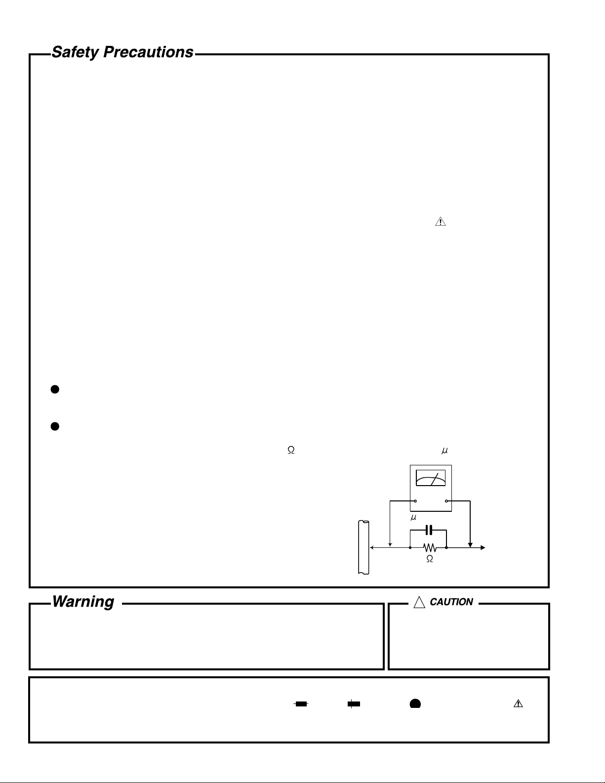
5. Leakage currnet check (Electrical shock hazard testing)
After re-assembling the product, always perform an isolation check on the exposed metal parts of the product
(antenna terminals, knobs, metal cabinet, screw heads, headphone jack, control shafts, etc.) to be sure the
product is safe to operate without danger of electrical shock.
Do not use a line isolation transformer during this check.
Plug the AC line cord directly into the AC outlet. Using a "Leakage Current Tester", measure the leakage
current from each exposed metal parts of the cabinet, particularly any exposed metal part having a return
path to the chassis, to a known good earth ground. Any leakage current must not exceed 0.5mA AC (r.m.s.).
Alternate check method
Plug the AC line cord directly into the AC outlet. Use an AC voltmeter having, 1,000 ohms per volt or more
sensitivity in the following manner. Connect a 1,500 10W resistor paralleled by a 0.15 F AC-type capacitor
between an exposed metal part and a known good earth ground.
Measure the AC voltage across the resistor with the AC
voltmeter.
Move the resistor connection to each exposed metal part,
particularly any exposed metal part having a return path to
the chassis, and meausre the AC voltage across the resistor.
Now, reverse the plug in the AC outlet and repeat each
measurement. Voltage measured any must not exceed 0.75 V
AC (r.m.s.). This corresponds to 0.5 mA AC (r.m.s.).
0.15 F AC TYPE
1500 10W
Good earth ground
AC VOLTMETER
(Having 1000
ohms/volts,
or more sensitivity)
Place this
probe on
each exposed
metal part.
!
1. This equipment has been designed and manufactured to meet international safety standards.
2. It is the legal responsibility of the repairer to ensure that these safety standards are maintained.
3. Repairs must be made in accordance with the relevant safety standards.
4. It is essential that safety critical components are replaced by approved parts.
5. If mains voltage selector is provided, check setting for local voltage.
Burrs formed during molding may
be left over on some parts of the
chassis. Therefore, pay attention to
such burrs in the case of
preforming repair of this system.
In regard with component parts appearing on the silk-screen printed side (parts side) of the PWB diagrams, the
parts that are printed over with black such as the resistor ( ), diode ( ) and ICP ( ) or identified by the " "
mark nearby are critical for safety.
(This regulation does not correspond to J and C version.)
1-2
Page 3
VS-DT2000
Preventing static electricity
1. Grounding to prevent damage by static electricity
Electrostatic discharge (ESD), which occurs when static electricity stored in the body, fabric, etc. is discharged,
can destroy the laser diode in the traverse unit (optical pickup). Take care to prevent this when performing repairs.
2. About the earth processing for the destruction prevention by static electricity
Static electricity in the work area can destroy the optical pickup (laser diode) in devices such as CD players.
Be careful to use proper grounding in the area where repairs are being performed.
2-1 Ground the workbench
Ground the workbench by laying conductive material (such as a conductive sheet) or an iron plate over it
before placing the traverse unit (optical pickup) on it.
2-2 Ground yourself
Use an anti-static wrist strap to release any static electricity built up in your body.
(caption)
Anti-static wrist strap
Conductive material
(conductive sheet) or iron plate
3. Handling the optical pickup
In order to maintain quality during transport and before installation, both sides of the laser diode on the
1.
replacement optical pickup are shorted. After replacement, return the shorted parts to their original condition.
(Refer to the text.)
Do not use a tester to check the condition of the laser diode in the optical pickup. The tester's internal power
2.
source can easily destroy the laser diode.
4. Handling the traverse unit (optical pickup)
1.
Do not subject the traverse unit (optical pickup) to strong shocks, as it is a sensitive, complex unit.
2.
Remove solder of the short land on the flexible wire after replacing the optical pickup. For specific details, refer
to the replacement procedure in the text. Remove the anti-static pin when replacing the traverse unit.
Be careful not to take too long a time when attaching it to the connector.
3.
Handle the flexible wire carefully as it may break when subjected to strong force.
4.
It is not possible to adjust the semi-fixed resistor that adjusts the laser power. Do not turn it.
5. Attention when traverse unit is decomposed
*Please refer to "Disassembly method" in the text for the CD pickup unit.
Short land
Apply solder to the short land before the flexible wire is disconnected
from the connector on the CD pickup unit.
(If the flexible wire is disconnected without applying solder, the CD
pickup may be destroyed by static electricity.)
In the assembly, be sure to remove solder from the short land after
connecting the flexible wire.
Flexible wire
CN601
CD servo board
1-3
Page 4
VS-DT2000
Important for laser products
1.CLASS 1 LASER PRODUCT
2.DANGER : Invisible laser radiation when open and inter
lock failed or defeated. Avoid direct exposure to beam.
3.CAUTION : There are no serviceable parts inside the
Laser Unit. Do not disassemble the Laser Unit. Replace
the complete Laser Unit if it malfunctions.
4.CAUTION : The compact disc player uses invisible
laserradiation and is equipped with safety switches
whichprevent emission of radiation when the drawer is
open and the safety interlocks have failed or are de
feated. It is dangerous to defeat the safety switches.
VARNING : Osynlig laserstrålning är denna del är öppnad
och spårren är urkopplad. Betrakta ej strålen.
VARO : Avattaessa ja suojalukitus ohitettaessa olet
alttiina näkymättömälle lasersäteilylle.Älä katso
säteeseen.
5.CAUTION : If safety switches malfunction, the laser is able
to function.
6.CAUTION : Use of controls, adjustments or performance of
procedures other than those specified herein may result in
hazardous radiation exposure.
CAUTION
!
Please use enough caution not to
see the beam directly or touch it
in case of an adjustment or operation
check.
ADVARSEL : Usynlig laserstråling ved åbning , når
sikkerhedsafbrydere er ude af funktion. Undgå
udsættelse for stråling.
ADVARSEL : Usynlig laserstråling ved åpning,når
sikkerhetsbryteren er avslott. unngå utsettelse
for stråling.
1-4
Page 5
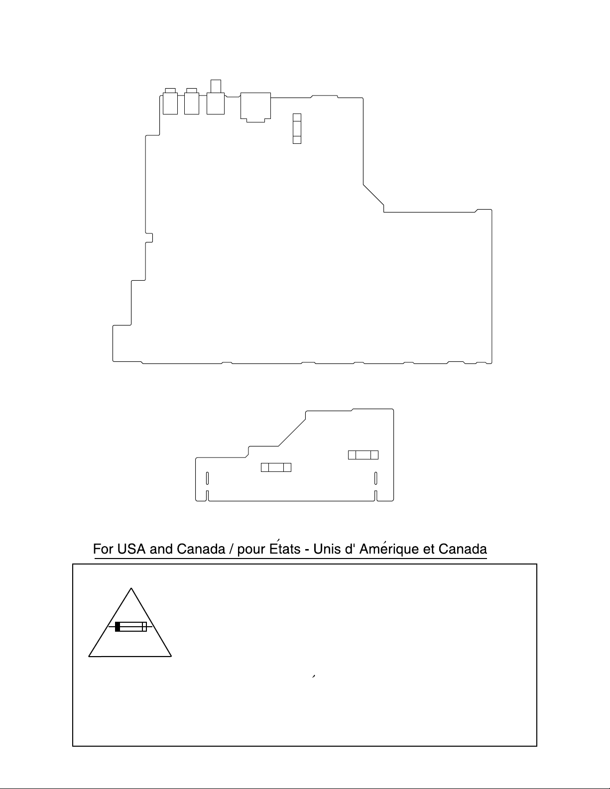
Importance administering point on the safety
<Main body section>
F1901
VS-DT2000
Main board
F1902
F1903
Power amplifier board
Caution: For continued protection against risk of
fire, replace only with same type 1A/125V for F1901,
8A/125V for F1902, 3.15A/125V for F1903.
This symbolspecifies type of fast operating fuse.
Precaution: Pour eviter risques de feux, remplacez
le fusible de surete de F1901 comme le meme type
que 1A/125V, F1902 comme le meme type que
8A/125, et 3.15A/125V pour F1903.
Ce sont des fusibles suretes qui functionnes rapide.
1-5
Page 6
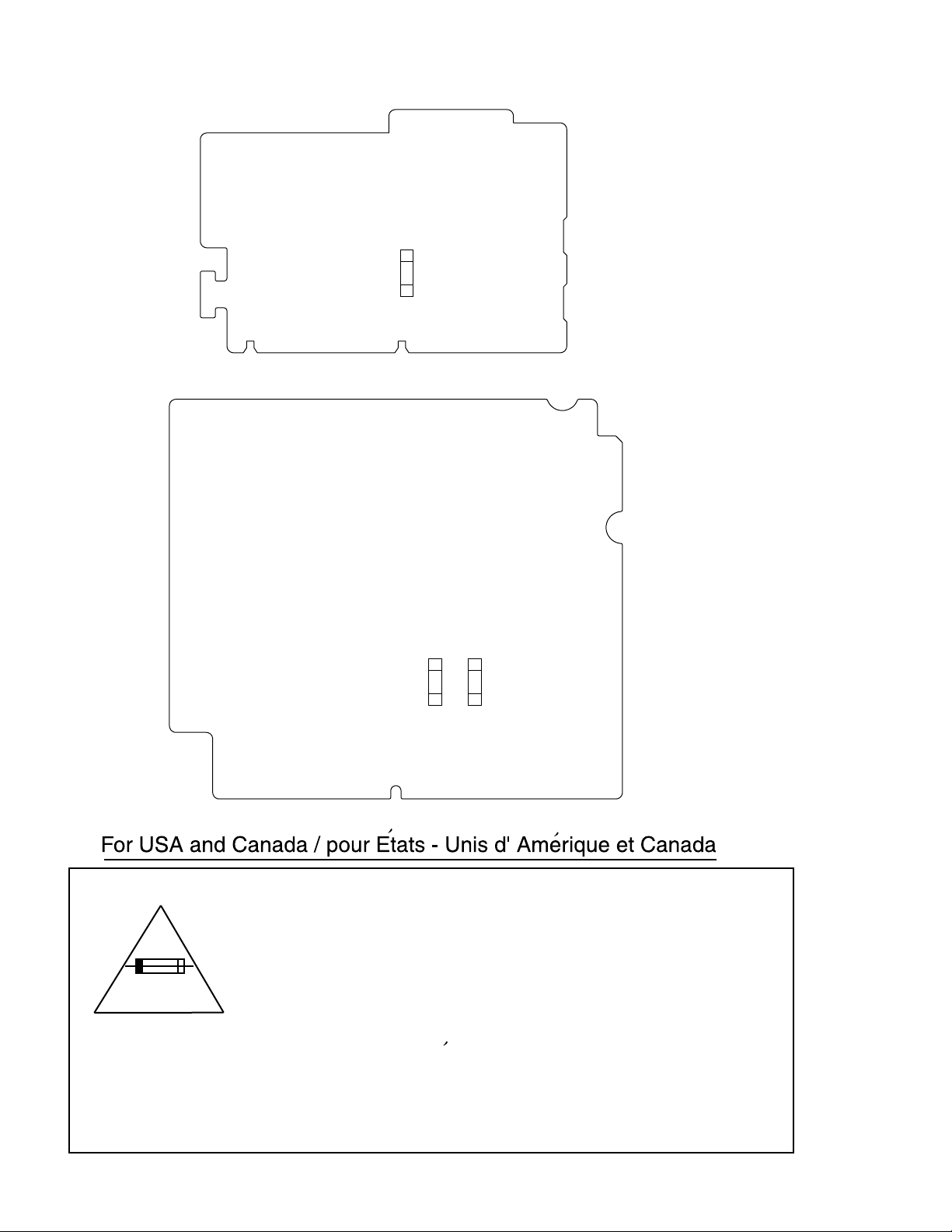
VS-DT2000
<Speaker section>
F2901
Switch board
F2911
F2921
Power supply board
Caution: For continued protection against risk of
fire, replace only with same type 2A/125V for F2901,
1.6A/125V for F2911, 1.6A/125V for F2921.
This symbolspecifies type of fast operating fuse.
Precaution: Pour eviter risques de feux, remplacez
le fusible de surete de F2901 comme le meme type
que 2A/125V, F2911 comme le meme type que
1.6A/125, et 1.6A/125V pour F2921.
Ce sont des fusibles suretes qui functionnes rapide.
1-6
Page 7
VS-DT2000
Disassembly method
<Main body section>
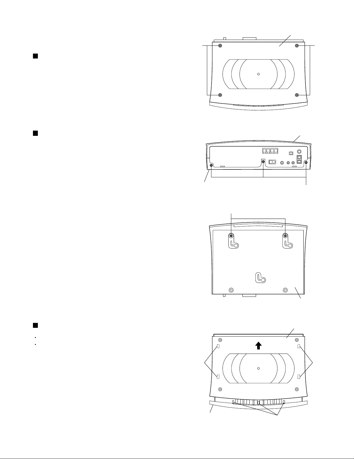
Removing the top lens (See Fig. 1.)
From the top side of the main body, remove the
four screws A attaching the top lens.
Removing the bottom panel
(See Figs. 2 and 3.)
1.
From the rear side of the main body, remove the
three screws B attaching the bottom panel.
2.
From the bottom side of the main body, remove the
two screws C attaching the bottom panel.
3.
Remove the bottom panel in an upward direction.
A
Bottom panel
Top lens
A
Fig.1
Top panel
B
Fig.2
Removing the top panel (See Fig. 4.)
Remove the top lens.
Remove the bottom panel.
1.2.Slide the top panel toward the rear (direction of the
arrow), disengage it from the engagement sections
a of the front panel assembly and engagement
sections b of the bottom chassis.
C
Bottom panel
Fig.3
Top panel
bb
Remove the top panel in an upward direction.
Front panel assembly
Fig.4
a
1-7
Page 8
VS-DT2000
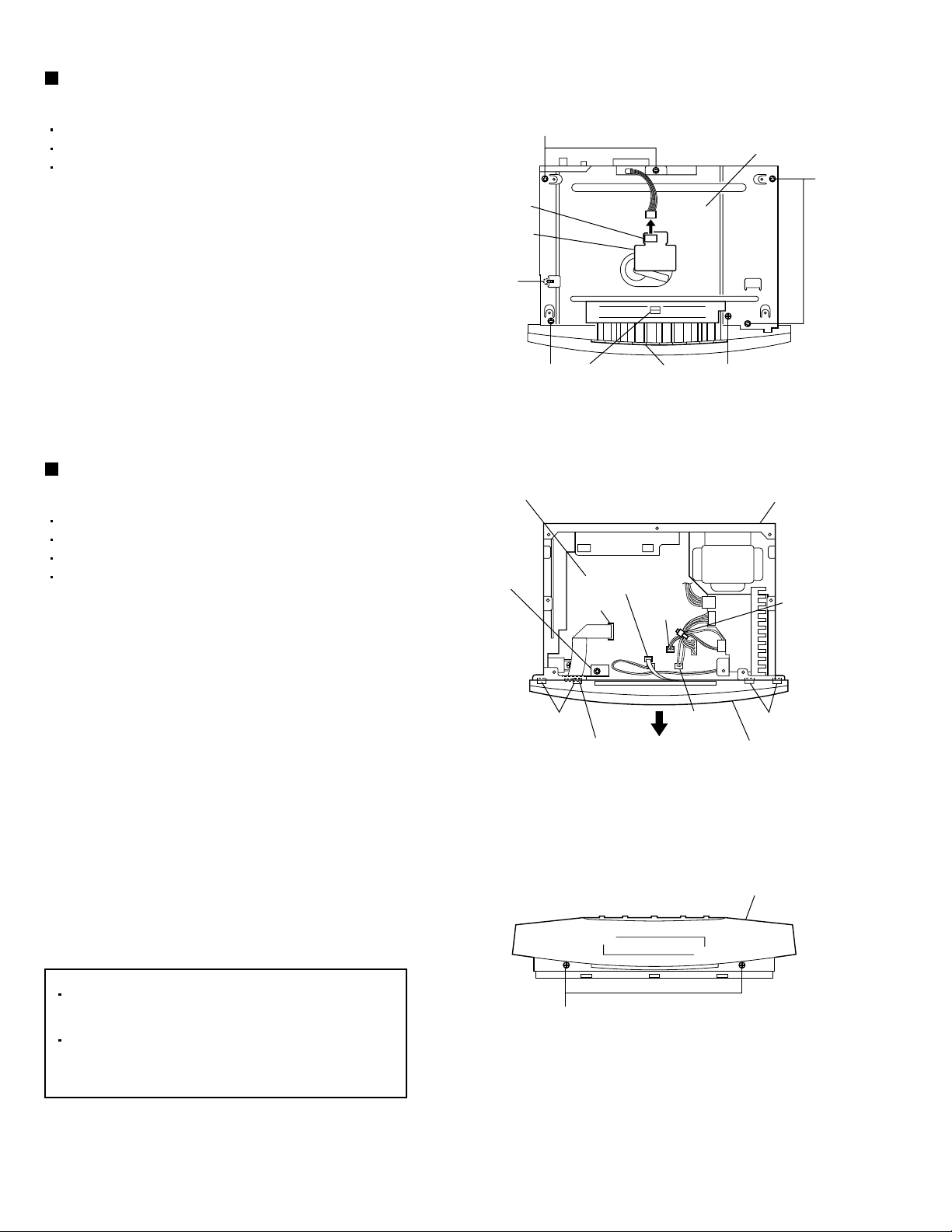
Removing the CD mechanism
assembly (See Fig. 5.)
Remove the top lens.
Remove the bottom panel.
Remove the top panel.
1.
From the top side of the main body, disengage the
claw c of the CD mechanism assembly and then
remove the push button.
2.
Remove the five screws D, screw E and screw F
attaching the CD mechanism assembly.
3.
Disconnect the wire from connector CN801 on the
LED board.
4.
Remove the CD mechanism assembly in an
upward direction.
Removing the front panel assembly
(See Figs. 6 and 7.)
CN801
LED board
F
Main board
D
D
Claw c
Push button
Fig.5
CD mechanism
assembly
D
E
Bottom chassis
Remove the top lens.
Remove the bottom panel.
Remove the top panel.
Remove the CD mechanism assembly.
1.
Remove the tie band bundling the wires of the front
panel assembly.
2.
Disconnect the wires from connectors CN106 and
CN182 on the main board.
3.
Disconnect the card wires from connectors CN171
and CN183 on the main board.
4.
Remove the wire holder holding the card wire of
the front panel assembly.
5.
From the front side of the main body, remove the
two screws G attaching the front panel assembly.
6.
Disengage the claws d of the front panel assembly
from the bottom chassis and then remove the front
panel assembly in the direction of arrow.
Wire holder
CN183
CN171
Claws d
Hole on
the bottom chassis
CN182
Fig.6
Tie band
CN106
Front panel assembly
Front panel assembly
Claws d
[Reference]
Before attaching the front panel assembly,
pass the card wire of the front panel assembly
through the hole on the bottom chassis.
After attaching the front panel assembly,
bundling the card wire and wires of the front
panel assembly using a wire holder and tie
band.
1-8
G
Fig.7
Page 9
Removing the tuner board
(See Figs. 8 and 9.)
Remove the top lens.
Remove the bottom panel.
Remove the top panel.
Remove the CD mechanism assembly.
1.
Disconnect the card wire from connector CN111 on
the main board.
2.
From the rear side of the main body, remove the
two screws H attaching the FM/AM antenna
terminals on the tuner board.
3.
Take out the tuner board from the bottom chassis.
Speaker board
CN102
Tuner board
Bottom chassis
Notch
Tie band
CN111
Fig.8
CN101
VS-DT2000
CD mechanism
assembly wire
Tie band
Main board
Removing the speaker board
(See Figs. 8 and 9.)
Remove the top lens.
Remove the bottom panel.
Remove the top panel.
Remove the CD mechanism assembly.
1.
Remove the tie bands bundling the wires on the
speaker board.
2.
Disconnect the wires from connectors CN101 and
CN102 on the speaker board.
3.
From the rear side of the main body, remove the
three screws J attaching the speaker/digital out
terminals on the speaker board.
4.
Take out the speaker board from the bottom
chassis.
[Reference]
After connecting the wires to the speaker
board, bundle them using a tie band.
Insert the CD mechanism assembly wire into
the notch on the bottom chassis. (See Fig. 8.)
Rear panel
Speaker terminal Digital out terminal
JH
Fig.9
FM antenna
terminal
AM antenna
terminal
H
1-9
Page 10
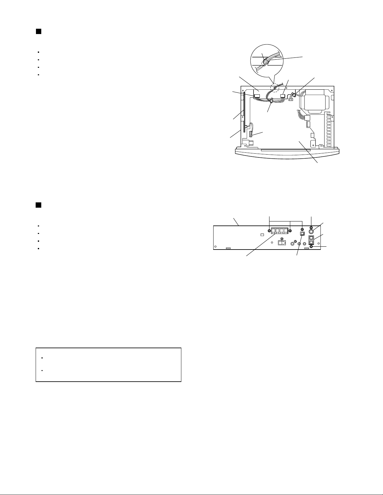
VS-DT2000
Removing the main board
(See Figs. 10 and 11.)
Remove the top lens.
Remove the bottom panel.
Remove the top panel.
Remove the CD mechanism assembly.
Remove the front panel assembly.
Remove the tuner board.
Remove the speaker board.
1.
Disconnect the wire from connector CN192 on the
power amplifier board.
2.
Disengage the wire clamp bundling the wire of the
power transformer.
3.
Disconnect the wires from connectors CN181,
CN191 and CN194 on the main board.
4.
Remove the screw K, which retains the main
board, together with the wire holder.
5.
Remove the two screws L, screw L' and screw M
attaching the main board.
6.
Remove the two screws N attaching the main
board and then remove the rear panel.
L
M
Wire holder
Main board
CN191
CN194
CN181
Rear panel
CN192
Fig.10
Power transformer
Wire clamp
L
Power amplifier
board
L'K
Bottom chassis
Earth wire
N
7.
Take out the main board from the bottom chassis.
[Reference] Attaching the main board
When attaching the screw L', attach the earth
wire of the main board at the same time.
When attaching the screw K, also attach the
wire holder together with it.
After connecting the wires to the connectors
CN192 and CN193 on the power amplifier
board, bundle them using wire holder.
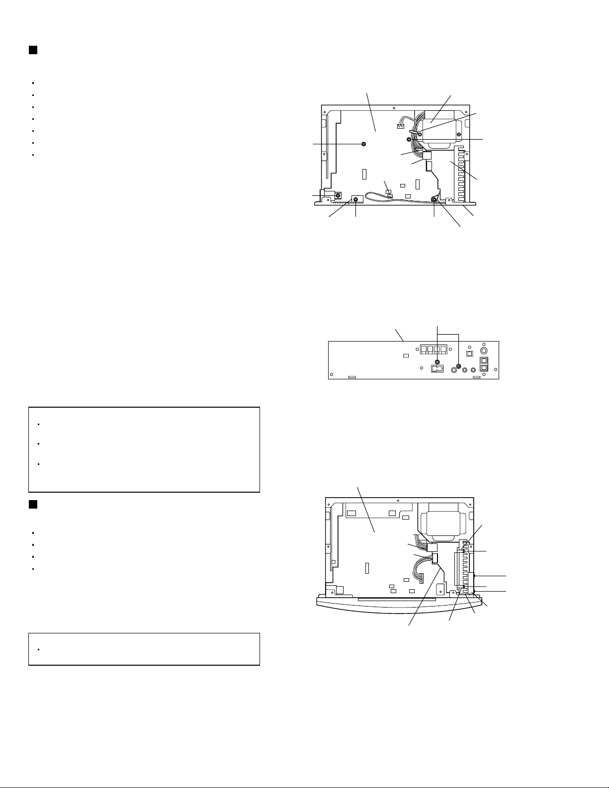
Removing the power amplifier board
(See Fig. 12.)
Remove the top lens.
Remove the bottom panel.
Remove the top panel.
Remove the CD mechanism assembly.
1.2.Disconnect the wires from connectors CN192 and
CN193 on the power amplifier board.
Remove the two screws P attaching the fan motor.
[Reference]
It is not necessary to remove the wire from
the fan motor.
3.4.Remove the two screws Q attaching the power
amplifier board.
Main board
Power amplifier
board
CN192
CN193
Fig.11
Fig.12
Hook e
Hook e
Q
Q
Fan motor
Heat sink
P
P
Lift the power amplifier board, disengage the two
hooks e from the heat sink of the main board and
take out the power amplifier board.
1-10
Page 11
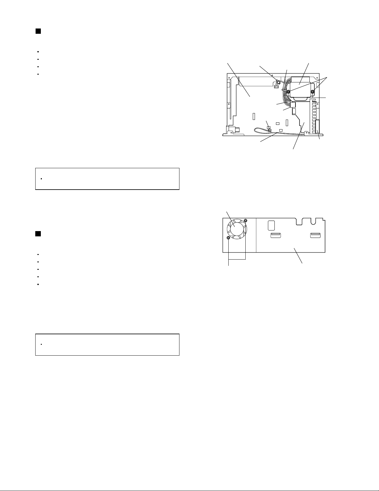
Removing the power transformer
(See Fig. 13.)
Remove the top lens.
Remove the bottom panel.
Remove the top panel.
Remove the CD mechanism assembly.
1.
Disengage the wire clamp and tie band bundling
the wires of the power transformer.
2.
Disconnect the wire from connector CN192 on the
power amplifier board.
3.
Disconnect the wires from connectors CN191 and
CN194 on the main board.
4.
Remove the two screws R and two washers
attaching the power transformer.
[Reference]
After connecting the wires, bundling them
using a wire clamp and tie band.
Main board
Treat the wire from the fan motor.
Tie band
CN194
CN181
Wire clamp
CN191
CN192
Power amplifier
board
Fig.13
VS-DT2000
Power transformer
Washers
R
Fan motor
Removing the fan motor
(See Figs. 13 and 14.)
Remove the top lens.
Remove the bottom panel.
Remove the top panel.
Remove the CD mechanism assembly.
Remove the front panel assembly.
1.2.Disconnect the wire from connector CN181 on the
main board.
From the right side of the main body, remove the
two screws P attaching the fan motor.
[Reference]
After mounting the fan motor, treat the wire
from the fan motor as shown in fig. 13.
Fan motor
P
Bottom chassis
Fig.14
1-11
Page 12

VS-DT2000
<Front panel assembly section>
Remove the top lens.
Remove the bottom panel.
Remove the top panel.
Remove the CD mechanism assembly.
Remove the front panel assembly.
Removing the switch board
(See Fig. 15.)
From the back side of the front panel assembly,
remove the four screws S attaching the switch
board.
Removing the open/close board
(See Figs. 15 and 16.)
1.2.From the back side of the front panel assembly,
remove the two screws T attaching the door motor
assembly.
Remove the screw W attaching the open/close
board of the door motor assembly.
Removing the door motor (See Fig. 16.)
Remove the door motor assembly.
1.
Remove the stop washers attaching the clutch
assembly and gear 2.
2.
Remove the clutch assembly, washer and Gear 2.
Door motor assembly
T
Clutch assembly
Stop washer
Gear 2
Front panel assembly
(Back side)
Front panel assembly
(Back side)
Fig.15
Door motor
Washer
Fig.16
Rod gear assembly
S
Switch board
X
W
Open/Close
board
Door motor assembly
f
3.
Remove the two screws X attaching the door
motor.
Removing the front board
(See Figs. 17 to 20.)
1.
While widening section f of the front base in the
direction of the arrow, remove the rod gear
assembly.
2.
Slide the moving panel assembly all the way in the
direction of the arrow.
3.
While slightly widening sections g toward the front,
take out the moving panel assembly in the direction
of the arrow.
4.
Remove the two screws Y attaching the moving
base of the moving panel assembly.
5.
Disengage the engagement sections h on the
inside of the moving base and at the inside of the
moving panel assembly and remove the moving
base.
6.
Remove the screw Z and screw Z' attaching the
front board.
7.
Disengage the claws i of the moving panel and
remove the front board.
[Reference]
Before attaching the moving base, pass the
card wire of the front board through the hole
on the moving base. (See Fig.19.)
When attaching the screw Z', attach the wire
at the same time.
Y
Z
Fig.17
Fig.18
Fig.19
Fig.20
g
Moving panel assembly
Moving base
Hole
i
Front board
Z'
Moving panel
Front base
Front base
hh
Card wire
Wire
1-12
Page 13

VS-DT2000
<CD mechanism assembly section>
Removing the LED board (See Fig. 1.)
From the top side of the CD mechanism assembly,
disengage the claw a of the top chassis attaching
the LED board and then remove the LED board.
Removing the CD mechanism
assembly (See Fig. 2.)
From the back side of the CD mechanism
1.
assembly, remove the three screws A attaching the
CD mechanism assembly on the top chassis.
Raise the protector in the direction of arrow and
2.
then remove the CD mechanism assembly.
Removing the CD servo board
(See Fig. 3.)
Claw a
A
LED board
Top chassis
Fig.1
CD mechanism assembly
[Caution] Be sure to solder the short land
section b on the flexible wire before
disconnecting the flexible wire from
connector CN601 on the CD servo
board.
If the flexible wire is disconnected
without attaching solder, the pickup
unit may be destroyed by static
electricity.
1.
From the back side of the CD mechanism
assembly, attach solder to the short land section b
of the flexible wire that is connected to the
connector CN601 of the CD servo board.
2.
Disconnect the flexible wire from connector CN601
on the CD servo board.
3.
Disconnect the card wires from connectors CN611
and CN612 on the CD servo board.
4.
Remove the two screws B attaching the CD servo
board.
5.
Lift the front edge of the CD servo board slightly
and disengage it from the projection c and then
from the engagement section d.
Protector
Flexible wire
Projection
Fig.2
Short land section b
CN612
CN601
CN611
c
Top chassis
Engagement section
CD servo board
B
A
d
[Caution] In the assembly, be sure to remove
solder from the short land section b
after connecting the flexible wire.
Fig.3
1-13
Page 14

VS-DT2000
Removing the traverse mechanism
assembly (See Fig. 4.)
Remove the CD servo board.
1.
Remove the two screws C attaching the CD servo
board bracket.
2.
Remove the two screws D attaching the traverse
mechanism assembly.
3.
Disengage the claw e attaching the traverse
mechanism assembly and then take out the
traverse mechanism assembly.
Removing the pickup unit
(See Figs. 5 and 6.)
Remove the CD servo board.
Remove the traverse mechanism assembly.
Traverse mechanism
assembly
Claw e
Pickup unit
E
Fig.4
C
DD
Section f
CD servo board
bracket
1.
From the top side of the traverse mechanism
assembly, remove the two screws E attaching the
shaft.
2.
From the traverse mechanism assembly, disengage
the section f of the pickup unit and then remove the
pickup unit with the shaft.
3.
Pull the shaft out of the pickup unit.
4.
Remove the screw F attaching the rack plate from
the pickup unit.
5.
Remove the screw G attaching the P.S. spring from
the pickup unit.
E
Shaft
Traverse mechanism assembly
Fig.5
Shaft
Pickup unit
P.S. spring
G
F
Rack plate
Fig.6
1-14
Page 15

VS-DT2000
Attaching the pickup unit
(See Figs. 7 and 8.)
[Reference]
Refer to the explanation of "Removing the
pickup unit" on the preceding page.
1.
Attach the P.S. spring and rack plate to the pickup
unit.
2.
Insert the shaft into the pickup unit.
3.
Engage the section f of the pickup unit with the
traverse mechanism assembly first, and set the
both ends of the shaft in the grooves g and h.
4.
After making sure that the section j of the rack plate
is meshed correctly with the middle gear, attach the
shaft using the two screws E.
Section f
Groove g
Groove h
Fig.7
Section j
E
Removing the traverse mechanism
board (See Fig. 9.)
Remove the CD servo board.
Remove the traverse mechanism assembly.
1.
From the back side of the traverse mechanism
assembly, disconnect the spindle motor wires and
feed motor wires that are soldered on the traverse
mechanism board.
2.
Remove the two screws H attaching the traverse
mechanism board.
Removing the feed motor (See Fig. 9.)
Rack prate
Fig.8
Traverse mechanism assembly
H
Spindle motor
Black
J
Feed motor
Red
Traverse
mechanism board
Red
H
Remove the CD servo board.
Remove the traverse mechanism assembly.
1.
From the back side of the traverse mechanism
assembly, disconnect the feed motor wires that are
soldered on the traverse mechanism board.
2.
Remove the two screws J attaching the feed motor.
Fig.9
1-15
Page 16

VS-DT2000
Removing the CD switch board
(See Fig.10.)
Remove the CD mechanism assembly.
1.
From the top side of the CD mechanism assembly,
remove the screw K attaching the CD switch board.
2.
Lift the CD switch board slightly and then remove
the wire from connector CN101 on the CD switch
board.
Removing the loading motor assembly
(See Figs.3, 10 to 12.)
CD mechanism assembly Clamper base assembly
K
Remove the CD mechanism assembly.
1.
From the back side of the CD mechanism
assembly, disconnect the card wire from connector
CN612 on the CD servo board. (See Fig.3.)
2.
From the top side of the CD mechanism assembly,
remove the two screws L attaching the clamper
base assembly.
3.
Disconnect the wire from connector CN101 on the
switch board while lifting the clamper base
assembly slightly and remove the clamper base
assembly.
4.
Remove the three screws M attaching the roller
holder assembly and take out the roller holder
assembly.
5.
Disconnect the wires from connectors CN103 and
CN104 on the loading motor assembly.
6.
Remove the belt of the loading motor assembly.
7.
Remove the two screws N attaching the loading
motor assembly and take out the loading motor
assembly.
CN101
M
CD switch board
L
Fig.10
Fig.11
CN103
L
M
Roller holder
assembly
CN104
Loading motor assembly
1-16
N
N
Belt
Fig.12
Page 17

VS-DT2000
<Speaker section>
Removing the amplifier assembly
(See Figs. 1 and 2.)
1.2.From the rear side of the speaker main body,
remove the eleven screws A attaching the amplifier
assembly.
Remove the connectors from the speaker.
A
AA
Amplifier assembly
A
Fig.1
Removing the back panel (See Fig. 3.)
Remove the amplifier assembly.
1.2.Pull out the knob and remove it.
Remove the three screws B attaching the back
panel.
Connectors
Amplifier assembly
Fig.2
Knob
B
Back panel
Fig.3
1-17
Page 18

VS-DT2000
Removing the pre-amplifier board
(See Fig. 4.)
Remove the amplifier assembly.
Remove the back panel.
1.
Remove the two screws C attaching the preamplifier board from the volume bracket.
2.
Disengage the tie band bundling the wires from the
power transformer.
3.
Disconnect the connector CN211 on the preamplifier board from the power supply board.
4.
Disconnect the wire from connector CN251 on the
pre-amplifier board.
Removing the power supply board
(See Fig. 5.)
Remove the amplifier assembly.
Remove the back panel.
Remove the pre-amplifier board.
1.
Remove the five screws D attaching the power
supply board.
2.
Remove the screw E attaching the power supply
board and wire holder.
Power supply board
D
CN281
E
Switch board
Volume bracket
C
CN211
Pre-amplifier
board
CN251
Tie band
Fig.4
D
Power supply
board
CN291
D
3.
Disconnect the wires from connectors CN281 and
CN291 on the power supply board.
Removing the switch board
(See Fig. 6.)
Remove the amplifier assembly.
Remove the back panel.
Remove the pre-amplifier board.
Remove the power supply board.
1.
Remove the three screws F attaching the AC
bracket.
2.
Disengage the tie band bundling the wires from the
power transformer.
3.
Disconnect the wire from connector CN299 on the
switch board.
Wire holder
Tie band
CN299
Switch board
F
F
Power transformer
Fig.5
Power
transformer
AC bracket
Fig.6
1-18
Page 19

Removing the power transformer
(See Figs. 7 and 8.)
Remove the amplifier assembly.
Remove the back panel.
Remove the pre-amplifier board.
Remove the power supply board.
1.2.Remove the two screws G attaching the cord cover.
Remove the four screws H and four washers
attaching the power transformer.
VS-DT2000
Cord cover
G
Fig.7
Removing the LED board
(See Figs. 9 and 10.)
1.
From the top of the speaker main body, insert the
tip of a flat-blade screwdriver or a similar tool into
the gap between the speaker main body and the
ornament window (sections a) in order to lift the
ornament window little by little so that it is
separated from the speaker main body. Then,
remove the ornament window in the direction of the
arrow.
2.
From the back side of the ornament window,
remove the two screws J attaching the LED board.
3.
Disconnect the wire from connector CN061 on the
LED board.
Washers
Fig.8
Section a Section a
Ornament window
Fig.9
Ornament window (Back side)
H
Washer
Power
transformer
Washer
H
J
LED board
Fig.10
CN061
1-19
Page 20

VS-DT2000
Flow of functional operation until TOC read
Power ON Play Key
Slider turns REST
SW ON.
Automatic tuning
of TE offset
Laser ON
Detection of disc
Automatic tuning of
Focus offset
Check Point
Confirm that the voltage at the pin3
of CN611 is "H"\"L"\"H".
Tracking error waveform at TOC reading
Pin 20 of
IC601(TEOUT)
Approx
1.8V
VREF
Disc states
to rotate
Approx.3sec
Tracking
servo
off states
Automatic measurement
of TE amplitude and
automatic tuning of
TE balance
Tracking
servo
on states
Disc to be
braked to stop
TOC reading
finishes
500mv/div
2ms/div
Fig.1
Automatic measurement of
Focus S-curve amplitude
Disc is rotated
Focus servo ON
(Tracking servo ON)
Automatic measurement of
Tracking error amplitude
Automatic tuning of
Tracking error balance
Automatic tuning of
Focus error balance
Confirm that the Focus error
S-curve signal at the pin 28 of
IC651 is approx.2Vp-p
Confirm that the signal from
pin 24 IC651(R808) is 0V as a
accelerated pulse during
approx.400ms.
Confirm the waveform of
the Tracking error signal
at the pin 20 of IC601 (R604)
(See Fig.1.)
1-20
Automatic tuning of
Focus error gain
Automatic tuning of
Tracking error gain
TOC reading
Play a disc
Confirm the eys-pattern
at the lead of TP1.
Page 21

Error code
Error code indication
Error code is indicated on the FL display.
This unit is placed horizontally.
SOURCE PRESET VOL
COMPACT COMPONENT SYSTEM
This unit is placed vertically.
VS-DT2000
SOURCE PRESET VOL
SOURCE PRESET VOL
Error code contents
FL indication
SOURCE PRESET VOL
COMPACT COMPONENT SYSTEM
Phenomenon
CD INIT ERR.
CD EJECT ERR
CD MECHA ERR
CD LOAD ERR.
Mechanism initialize error
Eject error / DISC abnormal equipment
Chucking switch error
Load error
1-21
Page 22

VS-DT2000
Maintenance of laser pickup
(1) Cleaning the pick up lens
Before you replace the pick up, please try to
clean the lens with a alcohol soaked cotton
swab.
(2) Life of the laser diode
When the life of the laser diode has expired,
the following symptoms will appear.
The level of RF output (EFM output : ampli
tude of eye pattern) will below.
Is the level of
RFOUT under
1.25V 0.22Vp-p?
YES
O.K
NO
Replace it.
Replacement of laser pickup
Turn off the power switch and, disconnect the
power cord from the ac outlet.
Replace the pickup with a normal one.(Refer
to "Removing the pickup unit" on the previous page)
Plug the power cord in, and turn the power on.
At this time, check that the laser emits for
about 3seconds and the objective lens moves
up and down.
Note: Do not observe the laser beam directly.
Play a disc.
Check the eye-pattern at TP1.
Finish.
(3) Semi-fixed resistor on the APC PC board
The semi-fixed resistor on the APC printed circuit board which is attached to the pickup is used to adjust the laser
power. Since this adjustment should be performed to match the characteristics of the whole optical block, do not
touch the semi-fixed resistor.
If the laser power is lower than the specified value, the laser diode is almost worn out, and the laser pickup should
be replaced.
If the semi-fixed resistor is adjusted while the pickup is functioning normally, the laser pickup may be damaged
due to excessive current.
1-22
Page 23

Description of major ICs
MN101C35DKB (IC811) : FL driver microcomputer
1. Terminal layout
100 76
1
75
VS-DT2000
25
26 50
2. Pin function
51
Pin No. Symbol I/O Function
1
2
3
4
5
6,7
8
9
10
11,12
13
14 23
24
25
26
27 30
31
32
33 38
39,40
41
42
43
44 46
47
48 60
61
62 64
65 99
100
NC
FLDATA
FLCLK
NC
FLCS
NC
B5V
OSC2
OSC1
GND
NC
GND
VREF
NC
FLRST
NCV70
REMCON_HO
NCV70
GND
NCV70
KEYLEDH
KEYLEDV
KEYDIMMER
NC
G1
G2 G14
G15
S1 S35
-VPP
-
Not connect
I/O
FL driver communication data input/output
I
FL driver communication clock input
-
Not connect
I
FL driver communication chip select input
-
Not connect
-
VDD(B5V)
O
8MHz main clock output
I
8MHz main clock input
-
Ground
-
Not connect
-
Ground
-
Reference voltage
-
Not connect
I
FL reset input
-
Not connect
O
Switching signal for receiver part of remote controller
-
Not connect
-
Ground
-
Not connect
-
Not use
-
Not use
-
Not use
-
Not connect
-
Not connect
O
Grid signal outputs
-
Not connect
-
Not connect
O
Segment signal outputs
-
VPP
BA15218F (IC102) : Dual operational amplifier
1. Terminal layout & Block diagram
OUT1
IN1-
IN1+
VEE
1
2
1
3
4
8
Vcc
7
OUT2
6
IN2-
2
5
IN2+
1-23
Page 24

VS-DT2000
MN101C30AKJ1 (IC701) : System control microcomputer
1. Terminal layout
64 49
1
48
16
17 32
2. Pin function
33
Pin No. Symbol I/O Function
1
2
3
4
5
6
7
8
9
10
11
12
13
14
15
16
17
18
19
20
21
22
23
24
25
26
27
28
29
30
31
32
33
34
35
36
37
38
39
40
THERM
KEY1
KEY2
VERSION
GND
VREF+
VDD
OSC2
OSC1
VSS
XI
XO
GND
CDTX
CDRX
FLRST
FLDATA
FLCS
FLCLK
STBLEDH
RST
STBLEDV
FTU
TUDATA
TUST
TUCK
MPX
RDSCK
RDSI
REM
GND
SMUTE
AHB
VOLDI
VOLCE
VOLCL
LOMUTE
TREMCONT
H-V
I
Temperature detection, ON/OFF control of FAN_SW signal(pin 57)
I
Key switch input of the main body
I
Key switch input of the main body
I
Switching signal for destination
-
Ground
-
Reference voltage for A/D converter (Connect to VDD.)
-
Power supply for microcomputer
O
8MHz main clock output
I
8MHz main clock input
-
Ground for microcomputer
I
32.768kHz sub clock input
O
32.768kHz sub clock output
-
Ground
O
CD(FMU-F1) communication
I
CD(FMU-F1) communication
O
FL reset output
I/O
FL driver communication data input/output
O
FL driver communication chip select output
O
FL driver communication clock output
O
Standby LED for horizontal establishment (POWER_OFF/ON=H)
I
Microcomputer reset input
O
Standby LED for vertical establishment (POWER_OFF/ON=H)
O
Power supply for tuner
I/O
PLL input/output data (Connect to tuner.)
O
PLL strobe output (Connect to tuner.)
O
PLL clock output (Connect to tuner.)
I
Stereo detection (Connect to tuner.), STEREO=L
-
Not use
-
Not use
I
Remote controller input
-
Ground
O
Mute signal, MUTE=L
O
Bass boost, ON=L, POWER_OFF=L
O
Data output (Connect to VOLUME_IC.)
O
Enable output (Connect to VOLUME_IC.)
O
Clock output (Connect to VOLUME_IC.)
O
Line out mute signal, MUTE=L
I
Remote controller effective signal for horizontal establishment, L : effective state
-
Connect to ground
I
Detecting signal for horizontal or vertical establishment
1-24
Page 25

VS-DT2000
Pin No. Symbol I/O
41
42
43
44
45
46
47
48
49
50
51
52
53
54
55
56
57
58
50
60
61
62
63
64
CDRSI
BLCTL
PSAVE
FCD
POUT
TOPLED1
TOPLED2
STBDIM
DOOR1
DOOR2
+BCTL
BUP
FANSW
MT0
MT1
MTS
VREFLOCK
SAFETYCD
SAFETY
-
-
-
O
-
-
O
O
O
O
O
O
O
O
O
-
Function
Connect to ground
Connect to ground
Connect to ground
CD reset output (Connect to FMU-F1.)
Connect to ground
Not connect
Power save mode ON/OFF signal, SAVE=H
CD power supply ON/OFF, not use
Main power supply ON/OFF
LED color control (Software PWN output)
LED color control (Software PWN output)
I
Dimmer control for STBYLED_H/V
I
Moving panel position detecting signal, CLOSE=L
I
Moving panel position detecting signal, OPEN=L
Unnecessary power supply cut-off signal for outage, Outage=H
I
Outage detecting signal (Backup mode)
Fan motor ON/OFF signal
Panel open (Motor driver)
Panel close (Motor driver)
Panel action speed (Not use)
Reference voltage for A/D converter (Connect to VSS.)
I
Detection signal for panel action load
I
Detecting signal for CD abnormal voltage
I
Detecting signal for abnormal voltage
KIA78S06P (IC702) : Regulator
1. Terminal layout 3. Block diagram
123
2. Pin function
Pin No.
1
2
3
Output
Common
Input
Function
Z1
Q14
Q16
Q1
R9
R10
R11
Q2
Q7
Q4
R1
Q3
Q6
R2
Q8
R3
UPC78L05J (IC191, IC261) : Three terminal voltage regulator
1. Terminal layout
1 : OUTPUT
2 : GND
3 : INPUT
123
2. Circuit diagram
R13
Q10
R14
R15
D1
Q15
R16
Q11
R1
Q1
R17
Q5
Q4
Q8
R4
R2
Q6
R5
C1
Q2
R3
C1
Q9
Q3
R9
R6
Q13
Q5
R4
Q9
Q7
Q10
D2
R19
R18
R11
Q12
Q11
Q12
R12
R7
R8
Q14
R10
Q13
R7
R5
R6
INPUT
OUTPUT
GND
3
INPUT
2
OUTPUT
1
COMMON
1-25
Page 26

VS-DT2000
MN662790RSC (IC651) : Digital servo & Digital signal prossesor
1. Terminal layout
20 1
21
80
40
41 60
2. Pin function
61
Pin No. Symbol I/O Function
1
2
3
4
5
6
7
8
9
10
11
12
13
14
15
16
17
18
19
20
21
22
23
24
25
26
27
28
29
30
31
32
33
34
35
36
37
38
39
40
BCLK
LRCK
SRDATA
DVDD1
DVSS1
TX
MCLK
MDATA
MLD
SENSE
FLOCK
TLOCK
BLKCK
SQCK
SUBQ
/DMUTE
STAT
DSP_RST
SMCK
CSEL
TEST2
TVD
PC
ECM
ECS
VDETMON
TRD
FOD
VREF
FBAL
TBAL
FE
TE
RF ENV
TEST3
OFT
TRCRS
/RFDET
BDO
LDON
O
Bit clock output for SRDATA
O
LR signal separation output
O
Serial data output
-
Power supply for digital circuit
-
GND for digital circuit
O
Digital audio ineterface output
I
Micro computer command clock signal input
I
Micro computer command data input
I
Micro computer command load signal input (L:Load)
-
Not use
-
Not use
-
Not use
O
Sub code block signal output
I
External clock input for sub code Q register input
O
Sub code Qdata output
I
Muting input (H:Mute)
O
Status signal input
I
Reset signal input (L:Reset)
-
Not use
I
Connect to DVDD1 (H fix)
-
Not use
O
Traverse drive output
-
Not use
O
Spindle motor drive signal (Enforced mode output)
O
Spindle motor drive signal (Servo error signal output)
-
Not use
O
Tracking drive output
O
Focus drive output
I
Reference voltage for D/A output block
O
Focus balance adjust signal output
O
Tracking balance adjust signal output
I
Focus error signal input (Analog input)
I
Tracking error signal input (Analog input)
I
RF envelope signal input (analog input)
I
Connect to GND
I
Off track signal input (H:Off track)
I
Track crosssignal input
I
RF detect signal input (L:Detect)
I
Drop out signal input (H:Drop out)
-
Not use
1-26
Page 27

Pin No. Symbol I/O Function
41
42
43
44
45
46
47
48
49
50
51
52
53
54
55
56
57
58
59
60
61
62
63
64
65
66
67
68
69
70
71
72
73
74
75
76
77
78
79
80
PLLF2
DSLBDA
WVEL
ARF
IREF
DRF
DSLF
PLLF
VCOF
AVDD2
AVSS2
EFM
DSLB
VCOF2
SUBC
SBCK
VSS
X1
X2
VDD
BYTCK
LD
GAIN
IPFLAG
FLAG
CLVS
CRC
DEMPH
RESY
IOSEL
/TEST
AVDD1
OUTL
AVSS1
OUTR
DQSY
Vcc5V
PSEL
MSEL
SSEL
-
Not use
-
Not use
-
Not use
I
RF signal input
I
Referrence current input
I
Bias pin for DSL
I/O
Loop filter pin for DSL
I/O
Loop filter pin for PLL
I/O
Loop filter pin for VCO
-
Power supply for analog circuit
-
GND for analog circuit
-
Not use
O
DSL balance output
I/O
Loop filter pin for Digtal servo VCO
-
Not use
-
Not use
-
GND for crystal oscillation circuit
I
Input for crystal oscillation circuit (f=16.9344MHz)
O
Output for crystal oscillation circuit (f=16.9344MHz)
-
Power supply for crystal oscillation circuit
-
Not use
O
Laser ON signal output (H : ON)
O
Gain control output (H : CD-RW)
-
Not use
O
Flag signal output
-
Not use
-
Not use
-
Not use
-
Not use
I
Mode select pin , Connect to DVDD1 (H fix)
I
Test pin ,Connect to DVDD1 (H fix)
-
Power supply for analog circuit
O
L-channel audio output
-
GND for analog circuit
O
R-channel audio output
-
Not use
-
Connect to power supply
I
IOSEL=H , Test pin , Connect to GND ( L fix)
I
IOSEL=H , SMCK output , Frequency select pin
I
IOSEL=H , SMCK output , SUBQ output mode select pin
VS-DT2000
LB1641 (IC108) : DC motor driver
1. Terminal layout
1
2 3 4 5 6 7 8 9 10
P1
VZ
IN1
GND
OUT1
IN2
VCC1
VCC2P2OUT2
2. Pin function
Input Output
IN1 IN2 OUT1 OUT2
1 0 1 0
0 1 0 1
1 1 0 0
Mode
Brake0 0 0 0
Clockwise
Counterclockwise
Brake
1-27
Page 28

VS-DT2000
UPD780024AGKB62 (IC251) : Unit microcomputer
1. Terminal layout
64 49
1
48
16
17 32
2. Pin function
33
Pin No. Symbol I/O Function
1
2
3
4
5
6
7
8
9
10
11
12
13
14
15
16
17
18
19
20
21
22
23
24
25
26
27
28
29
30
31
32
33
34
35
36
37
38
39
40
P50/A8
P59/A9
MCS
MRDY
CDINDEX
CDEMP
CDTNO
CDCOPY
VSSO
VDDO
P30
P31
P32
/DRMUTE
SUBQ
P35/SO31
SQCK
KCMND
M STAT
KCLK
RXDO
TXDO
P25/SCKO
VDD1
AVSS
VDTLV
P16/ANI6
PCHK
P14/ANI4
P13/ANI3
P12/ANI2
/REST
SW1
AVREF
AVDD
/RESET
XT2
XT1
IC
X2
-
Connect to ground
-
Not use
O
Synchronous/asynchronous output
I
Ready signal input
-
Not use
-
Not use
-
Not use
-
Not use
-
Ground terminal
-
Power supply terminal
-
Not use
-
Not use
-
Not use
O
Mute signal output
I
Sub code Q data input
-
Not use
O
Clock output for sub code Q register
I
Command signal input
O
CD control status output
I
CD control command clock input
I
Command input
O
Status output
-
Connect to ground
-
Power supply terminal
-
Ground terminal
I
Sensitivity adjustment for vibrating detection
-
Not use
I
Voltage monitor (for safety)
-
Connect to ground
-
Connect to ground
-
Connect to ground
I
Rest switch input
I
Mechanism switch (Photo sensor)
-
Reference voltage for analog circuit
-
Power supply terminal for analog circuit
I
CD control reset input
-
Not use
-
Connect to power supply
-
Connect to ground
-
Connect to external crystal oscillator
1-28
Page 29

Pin No. Symbol I/O Function
41
42
43
44
45
46
47
48
49
50
51
52
53
54
55
56
57
58
59
60
61
62
63
64
X1
VSS1
FLAG
BLKCK
/RFDET
EQx2
EQx4
P71/TIO1
FWD
REW
IREFx4
P75/BUZ
/RESET
S TAT
/DMUTE
/P.ON
MLD
M DATA
MCLK
P43/AD3
P44/AD4
P45/AD5
/SW2
/SW3
-
Connect to external crystal oscillator
-
Ground terminal
I
Flag signal input
I
Sub code block clock signal input
I
RF signal amplitude detecting signal input
I
Equalizer select signal input
I
Equalizer select signal input
-
Not use
O
Loading (EJECT) output
O
Loading (LOAD) output
O
Switching signal for IREF current (4x mode : L)
-
Not use
O
Reset signal output (L: reset)
I
Status signal input
O
Muting output
O
Power ON/OFF switching signal output
O
Microcomputer command load signal output
O
Microcomputer command data output
O
Microcomputer command clock signal output
-
Not use
-
Not use
-
Not use
I
Mechanism switch (Loading switch)
I
Mechanism switch (Chucking completion)
LA4905 (IC301) : 2ch BTL power IC
1. Terminal layput 2. Block diagram
CVL
C
SWB VL VL
8
9 15 14 12 13 16 7 5 6 18 19 17 22
SW
123
VH
11
drive
SW
GND
Amplifier
output
stage
+OUT1 +OUT2 NC-OUT1 -OUT 2PG1 PG2
AB D
VS-DT2000
C
D
H.L.S. :
C
B
A
Ripple
filter
Higher
Level signal
selector
Nonlinear/output stage
Input
amplifier
CH 1
BEEP
amplifier
Power supply/ground
shorting protection circuit
Overvoltage/thermal
VH
H.L.S.
Switching regulator
block
10
Standby
SW
ST-BY RF PREGND IN 1 IN 2 ON-TIMEBEEP
NJM4580D-D (IC101,IC211,IC212,IC213) : Dual operational amplifier
1. Terminal layout & Block diagram
8 7 6 5
B
A
1 2 3 4
1. A OUTPUT
2. A -INPUT
3. A +INPUT
-
4. V
5. B +INPUT
6. B -INPUT
7. B OUTPUT
+
8. V
protection circuit
CH 2
Input
amplifier
Nonlinear amplifier/output
stage
Pop noise
prevention
circuit
ON MUTE
muting circuit
2314322021
1-29
Page 30

VS-DT2000
AN22000A (IC601) : RF & Servo amplifier
1. Terminal layout 2. Block diagram
3TOUT
CEA
9 10 15 22 23 21 20 19 18 2 1
14
OFTR 3TENV
13
12
BDO
11
8
AGC
7
6
5
4
NRFDET
RF_EQ
10
11
12
13
14
15
16
1
2
3
4
5
6
7
8
9
32
31
30
29
28
27
26
25
24
23
22
21
20
19
18
17
OFTR
COFTR
BDO
CBDO
ARF
C.AGC
RF IN
RF OUT
RFN
FEN
FEOUT/RFDET
SUBT SUBT
BCA
GCA
BCA
GCA
TEN
BCA
GCA
AMPAMPAMP
VDET
TEBPFTEOUT
VDET
BCA
GCA
AMP
PDLD
3
VCC
16
GND
FBAL
25
26
TBAL
GCTRL
24
3. Pin function
A C B D PDE PDF VREF
Pin No. Symbol Function
1
2
3
4
5
6
7
8
9
10
11
12
13
14
15
16
17
18
19
20
21
22
23
24
25
26
27
28
29
30
31
32
PD
LD
VCC
RFN
RF OUT
RF IN
C.AGC
ARF
CEA
3TOUT
CBDO
BDO
COFTR
OFTR
/RFDET
GND
VREF
VDET
TEBPF
TEOUT
TEN
FEN
FEOUT
GCTRL
FBAL
TBAL
PDE
PDF
D
B
C
A
APC Amp. Input terminal
APC Amp.Output terminal
Power supply terminal
RF addition Amp.Reversing input terminal
RF addition Amp.Output terminal
AGC input terminal
Terminal of connection of capacity of AGC loop filter.
AGC output terminal
Capacity connection terminal for HPF-Amp.
3TENV output terminal
Capacity connection terminal for RF shade side envelope detection
BDO output terminal
Capacity connection terminal for RF discernment side envelope detection
OFTR output terminal
RFDET output terminal (Negative logic)
Earth terminal
VREF output terminal (Not use)
VDET output terminal (Not use)
VDET input terminal
TE Amp. output terminal
TE Amp. reversing input terminal
FE Amp. reversing input terminal
FE Amp. output terminal
Terminal GCTL & APC
FBAL control terminal
TBAL control terminal
Tracking signal input terminal 1
Tracking signal input terminal 2
Focus signal input terminal 4
Focus signal input terminal 2
Focus signal input terminal 3
Focus signal input terminal 1
2729303132
28
17
1-30
Page 31

LA1838 (IC1) : FM AM IF amplifier & Detector, FM MPX Decoder
1. Terminal layout & Block diagram
VS-DT2000
30
ALC
BUFF
FM
S-METER
FM IF
1
29
AM
OSC
S-CLRVE
PM
DET
2
SD
COMP
27
28
REG
AM
MIXFMRF.AMP
AM IF DET
AM/FM
IF-BUFF
4
3
26
AGC
AM
S-METER
GND
25
24
TUNING
DRIVE
5
STEREO
DRIVE
6
7
22
23
VCC
89
P-DET
384KHz
21
DECODER
ANIT-BIRDIE
VCO
10
2. Pin function
Pin No. Symbol I/O Function
This is an input terminal of FM IF signal.
1
2
3
4
5
6
7
8
9
10
11
12
13
14
15
16
17
18
19
20
21
22
23
24
25
26
27
28
29
30
FM IN
AM MIX
FM IF
AM IF
GND
TUNED
STEREO
VCC
FM DET
AM SD
FM VSM
AM VSM
MUTE/IFOUT
FM/AM
MONO/ST
LOUT
ROUT
LIN
RIN
RO
LO
MPX IN
FM OUT
AM DET
AM AGC
AFC
AM RF
REG
AM OSC
OSC BUFFER
I
This is an out put terminal for AM mixer.
O
Bypass of FM IF
I
Input of AM IF Signal.
I
This is the device ground terminal.
When the set is tunning,this terminal becomes "L".
O
Stereo indicator output. Stereo "L", Mono: "H"
O
This is the power supply terminal.
FM detect transformer.
This is a terminal of AM ceramic filter.
Adjust FM SD sensitivity.
O
Adjust AM SD sensitivity.
O
When the signal of IF REQ of IC121(LC72131) appear, the signal of FM/AM IF output.
I/O
Muting control input.
Change over the FM/AM input. "H" :FM, "L" : AM
I
Stereo : "H", Mono: "L"
O
Left channel signal output.
O
Right channel signal output.
O
Input terminal of the Left channel post AMP.
I
Input terminal of the Right channel post AMP.
I
Mpx Right channel signal output.
O
Mpx Left channel signal output.
O
Mpx input terminal
I
FM detection output.
O
AM detection output.
O
This is an AGC voltage input terminal for AM.
I
This is an output terminal of voltage for FM-AFC.
AM RF signal input.
I
Register value between pin 26 and pin28 besides the frequency width of the input signal.
O
This is a terminal of AM Local oscillation circuit.
AM Local oscillation Signal output.
O
20
STEREO
5N
SW
FF
38k
11
18
19
MUTE
FF
19k
/
2
12 13
FF
19k
17 16
/LS
14
PILOT
DET
15
1-31
Page 32

VS-DT2000
LA6575H (IC801) : Focus & Spindle & Feed & Tracking BTL driver
1. Terminal layout 2. Block diagram
1
2
3
4
5
6
7
FR
8
9
10
11
12
13
14
28
27
26
25
24
23
22
FR
21
20
19
18
17
16
15
REV
FWD
28 27 26 25 24 23 22 FR 21 20 19 18 17 16 15
Input
MUTE is as follows:
High: Output ON
Low : Output OFF
Thermal
shutdown
Output
control
CH5 CH4
CH5
POWER
1234567 FR 8 9 1011121314
VO5-
VCC2
3. Pin function
Pin No. Symbol Function
1
2
3
4
5
6
7
8
9
10
11
12
13
14
VCC2
VO5VO5+
VO4+
VO4VO3+
VO3VO2+
VO2VO1+
VO1VCC1
VIN1
VIN1G
Power supply for CH3/CH4/CH5
Loading output (-)
Loading output (+)
Tracking output (+)
Tracking output (-)
Focus output (+)
Focus output (-)
Spindle output (+)
Spindle output (-)
Traverse output (+)
Traverse output (-)
Power supply for CH1/CH2
Not use
Traverse drive input
S-GND
MUTE
MUTE
Level
shift
VO5+
VO4+
VIN4
VIN4G
22k 11k
VO4-
Signal
system
power
Level
shift
CH3
VO3+
VCCS
VO3-
VREF-IN
REG-OUT
5VREG
(External PNP_Tr)
Level
shift
CH2
VO2-
VO2+
Pin No. Symbol Function
15
16
17
18
19
20
21
22
23
24
25
26
27
28
VIN2
VIN2G
VIN3
VIN3G
REG-IN
REG-OUT
VREF-IN
VCCS
VIN4G
VIN4
MUTE
S-GND
FWD
REW
Not use
Spindle drive input
Not use
Focus drive input
Connect to power supply
Not use
Reference voltage input terminal
Signal system power
Tracking drive input
Not use
Mute for CH1/CH2/CH3/CH4
Signal system ground
Loading input (EJECT)
Loading input (LOAD)
REG-IN
VIN3G
22k
Level
shift
CH1
VO1-
VO1+
VIN3
11k
22k
11k
CH1- 4
POWER
VCC1
22k
VIN2G
VIN2
11k
VIN1
VIN1G
GP1FA550TZ (J3601) : Fiber optic transmitter/Receiver
1. Terminal layout 2. Block diagram
LED
Drive
IC
VIN
VCC
GND
1-32
Page 33

LC72136N (IC2) : PLL frequency synthesizer
1. Terminal layout
2. Block diagram
VS-DT2000
FM
CE
DI
CK
DO
LW
MW
SDIN
1
2
3
4
5
6
7
8
9
10
11
22
21
20
19
18
17
16
15
14
13
12
XIN
VSS
LPFOUT
LPFIN
PD
VDD
FMOSC
AMOSC
IF REQ
FM/AMIF
16
17
22
15
21
1
1/2
3
4
5
6
C2B
I/F
Power
on
Reset
Reference
Swallow Counter
1/16,1/17 4bit
Programmable
Data Shift Register & Latch
721113
XOUT
ST/MONO
AM/FM
3. Pin function
Pin No. Symbol I/O Function
1
2
3
4
5
6
7
8
9
10
11
12
13
14
15
16
17
18
XOUT
FM
CE
DI
CK
DO
ST/MONO
AM/FM
LW
MW
SDIN
FM/AM IF
IF REQ
AMOSC
FMOSC
VDD
PD
I
X'tal oscillator connect (75kHz)
O
LOW:FM mode
I
Chip enable, When data output/input for 4pin(input) and 6pin(output): H
I
Input for receive the serial data from controller
I
Sync signal input use
O
Data output for Controller, Output port
O
"Low": MW mode
O
Open state after the power on reset
I/O
Input/output port
I/O
Input/output port
I/O
Data input/output
I
IF counter signal input
O
IF signal output
-
Not use
I
AM Local OSC signal output
I
FM Local OSC signal input
-
Power supply(VDD=4.5-5.5V), When power ON:Reset circuit move
O
PLL charge pump output(H: Local OSC frequency Height than Reference
frequency. L: Low Agreement: Height impedance)
19
20
21
22
LPFIN
LPFOUT
VSS
XIN
I
Input for active low pass filter of PLL
O
Output for active low pass filter of PLL
-
Connected to GND
I
X'tal oscillator connect (75KHz)
Driver
12bit
Drivers
8
Phase
Detector
Charge Pump
Unlock
Detector
Universal
Counter
18
19
20
12
1-33
Page 34

VS-DT2000
LC75342M (IC501) : E. volume
1. Terminal layout
1
DATA
2
CE
3
VSS
4
TEST
5
ROUT
6
RBASS2
7
RBASS1
8
RTRE
9
RIN
10
RSELO
11
R4
12
R3
13
R2
14
R1
15
NS
3. Pin function
Pin No.
Symbol Function
1
DATA
2
3
4
5
6
7
8
9
10
11
12
13
14
15
16
CE
VSS
TEST
ROUT
RBASS2
RBASS1
RTRE
RIN
RSELO
R4
R3
R2
R1
NC
NC
2. Block diagram
RSELO RIN RTRE RBASS1 RBASS2 ROUT
30
29
28
27
26
25
24
23
22
21
20
19
18
17
16
CLOCK
VDD
VREF
NC
LOUT
LBASS2
LBASS1
LTRE
LIN
LSELO
L4
L3
L2
L1
NC
NC
NC
11
R4
12
R3
13
R2
14
R1
15
16
17
L1
18
L2
19
L3
20
L4
10
Serial data and clock input for IC
control
Chip enable
Connect to GND
Electric volume connection for test
Volume control and equalizer input
Connection for resistor and capacitor
that from the bass band filter
Connection for capacitor that from
the treble band filter
Volume control and equalizer input
Input selector output
Input signal connections
Input signal connections
Input signal connections, not use
Input signal connections
Not use
Not use
9 8 7 6 5
CONTROL
CIRCUIT
LOGIC
CIRCUIT
CONTROL
CIRCUIT
Pin No.
17
18
19
20
21
22
23
Symbol Function
L1
L2
L3
L4
LSELO
LIN
LTRE
LVref
CCB
INTERFACE
RVref
LOUTLBASS2LBASS1LTRELINLSELO
Input signal connections
Input signal connections, not use
Input signal connections
Input signal connections
Input selector output
Volume control and equalizer input
Connection for capacitor that from
the treble band filter
24
25
26
27
28
LBASS1
LBASS2
LOUT
VREF
Connection for resistor and capacitor
that from the bass band filter
Volume control and equalizer input
NC
Not use
Connection to the 0.5X VDD voltage
generator circuit used as the analog
signal ground
29
30
VDD
CLOCK
Power supply
Serial data and clock input for IC
control
4
TEST
3
VSS
2
CE
DATA
1
CLOCK
30
VDD
29
VREF
28
NC
27
262524232221
XC62HR3502P (IC291) : Regulator
1. Terminal layout 3. Pin function2. Block diagram
Vout (NC)
1
23
Vss Vin
1-34
45
ON/OFF
ON/OFF
Vin
2
3
Current limit
Output
control
Voltage
reference
5
1
Vout
GND
Pin No.
1V
2Vin
Symbol Function
SS
GND
Power supply input
3 ON/OFF ON/OFF control
4
(NC)
Not use
5 Vout Regulator output
Page 35

RPM6938-SV4 (IC801,IC812) : Remote control receiver
1. Block diagram
I/V
conversion
PD
magnetic shield
AMP
BPF
for
trimming circuit
AGC
Detector
Vcc
Comp
22k
ohm
VDD
OUT
GND
STK411-290E (IC221) : Power amplifier
1. Terminal layout
122
2. Block diagram
+VH
LIN
-LIN
NF1
17
18
19
20
TR1 TR2
C1
R2
TR3
TR5
R3
TR4
D6
R4
TR9
TR7
R8
R9
C5
TR11 TR23
TR12
TR10
TR24
TR22
TR6
C2
TR8
R5
R6
R7
D1
R19
C6
TR21
TR20
TR19
R18
R14
R16
R17
D7
R15
R16
TR14 TR13
C3
TR16
TR17
R13
R12
TR15
TR31
D31
D32
TR32
R31
Comparator
Comparator
D33
D35
D34
D36
VS-DT2000
1
+VH
3
NC
+VL comp
5
+VL
4
GND
2
SUB
-VL
7
-VL comp
6
R51
12 13
-VH
-VH
-VH
1511141016
LOUT
CH1-V
ROUT
CH2-V
TC74HCU04AP (IC251) : Inverter
1. Terminal layout & Block diagram 2. Truth table
11A
21Y
32A
42Y
53A
63Y
7
(TOP VIEW)
14
13
12
11
10
9
8GND
VCC
6A
6Y
5A
5Y
4A
4Y
INPUT INPUT
A
L
H
R32
22
21
9
-VL
RIN
-RIN
-VH
8
Y
H
L
1-35
Page 36

VS-DT2000
VICTOR COMPANY OF JAPAN, LIMITED
AUDIO & COMMUNICATION BUSINESS DIVISION
PERSONAL & MOBILE NETWORK BUSINESS UNIT. 10-1,1Chome,Ohwatari-machi,maebashi-city,371-8543,Japan
No.21082
200205
 Loading...