

Page 1
52169200310
SERVICE MANUAL
PDP COLOR TELEVISION
PD-42WX84 /SJ
TV
CATV VCRDVD
ASPECT
MULTI SCREEN
INDEX
SPLIT
FREEZE
SWAP SELECT
INPUT 1
V1
123
INPUT 2
V2
456
INPUT 3
V3
789
RETURN+
INPUT 4
100+
TV
0
V4
THEATER
NATURAL
VIDEO
DIGITAL-IN
PRO
CINEMA
STATUS
D-IN
SLEEP TIMER
DISPLAY SOUND
LIGHT
+
MUTING
C.C.
C.C.
CH
VOL
VOL
OK
CH
MENU
BACK
VCR CHANNEL
VCR DVD
PREV NEXT
POWER
TV VCR
REW
FFPLAY
REC PAUSE
STOP
OPEN CLOSE
STILL PAUSE
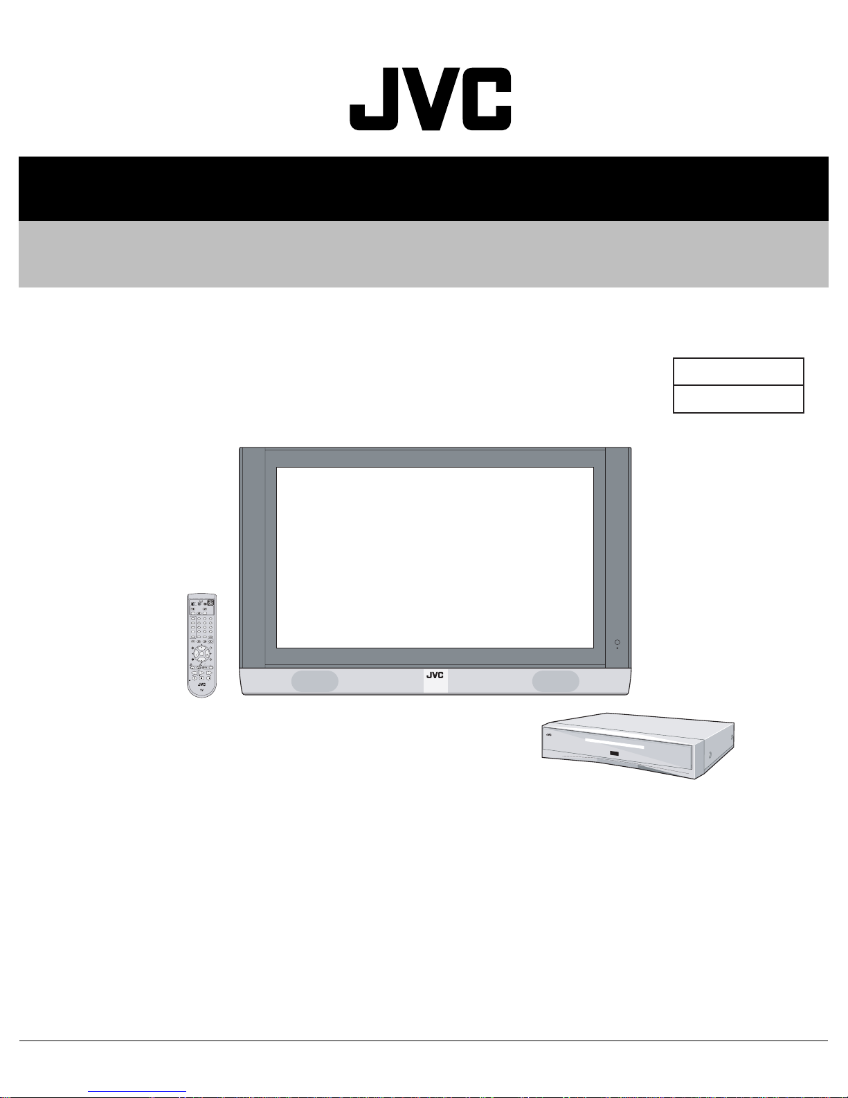
RM-C13G
VM-42WX84
[PLASMA DISPLAY UNIT]
BASIC CHASSIS
SB3
1 PRECAUTION. . . . . . . . . . . . . . . . . . . . . . . . . . . . . . . . . . . . . . . . . . . . . . . . . . . . . . . . . . . . . . . . . . . . . . . . . 1-3
2 SPECIFIC SERVICE INSTRUCTIONS. . . . . . . . . . . . . . . . . . . . . . . . . . . . . . . . . . . . . . . . . . . . . . . . . . . . . . 1-6
3 DISASSEMBLY . . . . . . . . . . . . . . . . . . . . . . . . . . . . . . . . . . . . . . . . . . . . . . . . . . . . . . . . . . . . . . . . . . . . . . 1-10
4 ADJUSTMENTS . . . . . . . . . . . . . . . . . . . . . . . . . . . . . . . . . . . . . . . . . . . . . . . . . . . . . . . . . . . . . . . . . . . . . . 1-21
5 TROUBLESHOOTING . . . . . . . . . . . . . . . . . . . . . . . . . . . . . . . . . . . . . . . . . . . . . . . . . . . . . . . . . . . . . . . . . 1-55
COPYRIGHT © 2003 VICTOR COMPANY OF JAPAN, LIMITED
TU-42WX84
[RECEIVER UNIT]
TABLE OF CONTENTS
No.52169
2003/10
Page 2

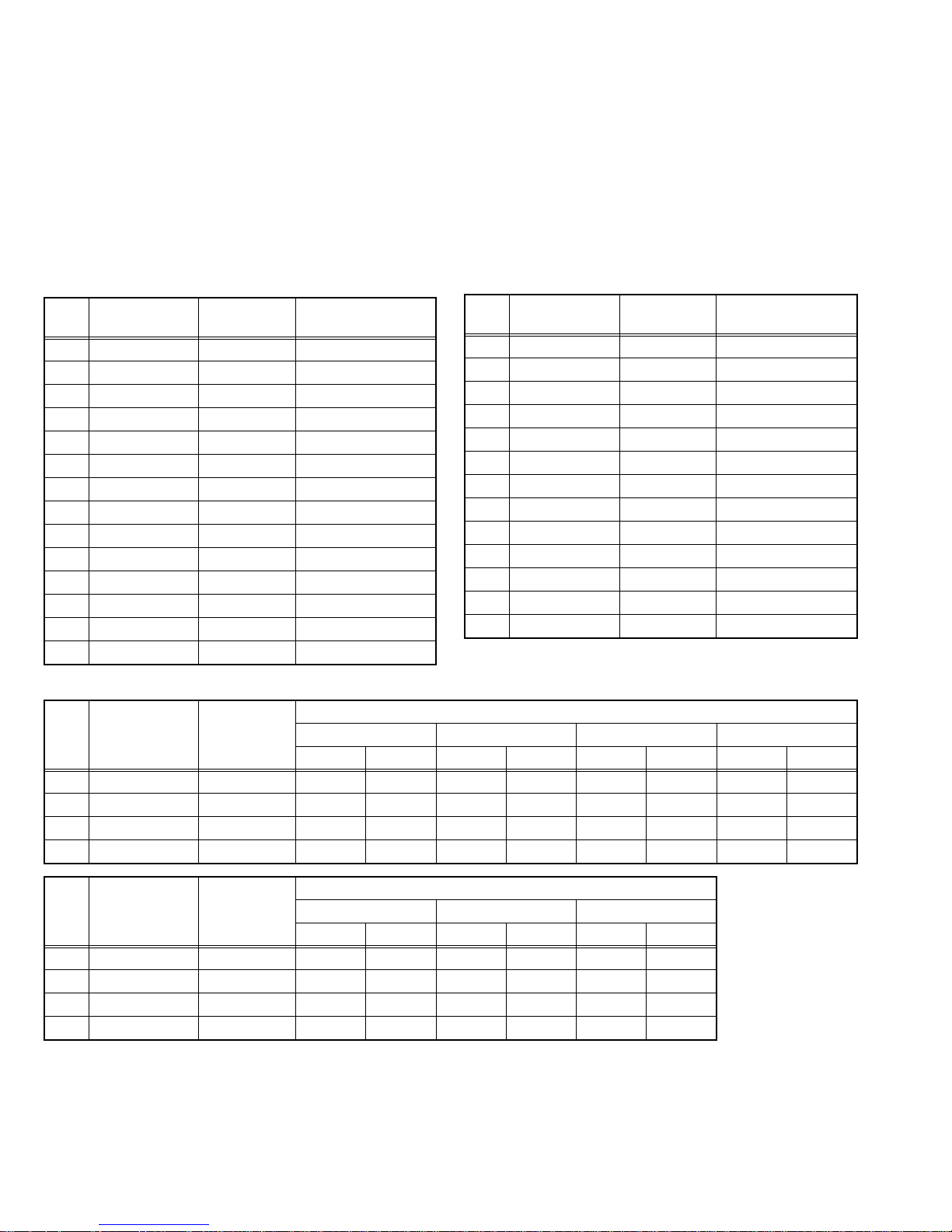
SPECIFICATION
Items Contents
Dimensions (W × H × D) Plasma display unit 116.0cm × 79.8cm × 30.8cm (45-11/16 × 31-7/16 × 12-3/16") [with the stand]
116.0cm × 73.1cm × 9.8cm (45-11/16 × 28-13/16 × 3-7/8") [main TV body]
Receiver unit 43.5cm × 9.9cm × 38.2cm (17-3/16 × 3-15/16 × 15-1/16")
Mass Plasma display unit 48kg (106lbs) [with the stand]
38kg (84lbs) [main TV body]
Receiver unit 5.1kg (11.3lbs)
TV RF System CCIR (M)
Color System NTSC
Sound System BTSC (Multi Channel Sound)
TV Receiving Channels and
Frequency
TV / CATV Total Channel 180 Channels
Intermediate Frequency Video IF
Color Sub Carrier 3.58 MHz
Power Input AC 120V, 60Hz
Power Consumption Plasma display unit
Plasma Display Panel (PDP) 42-inch wide aspect (16:9)
Screen Size Diagonal : 107.5cm (H:51.8cm × V : 105.7cm)
Display Pixels Horizontal : 1024 dots × Vertica l : 768 dots (XGA)
Audio Power Output 18W + 18W (Main/Woofer)
Speaker Main (DD)
Antenna terminal (VHF/UHF) F-type connector, 75Ω unbalanced, coaxial
Video / Audio input
Input-1/2/3/4
Component Video
Digital-in Video
Audio output
Sub woofer output 0~1000mV (rms), Low impedance, RCA pin jack × 1
AV compulink III 3.5mm mini jack × 1
Display Input / Output
(For system cable)
Remote Control Unit RM-C13G (AA/R6 /U M-3 battery × 2)
Design & specifications are subject to change without notice.
VHF Low
VHF High
UHF
CATV
Sound IF
Receiver unit
Woofer
S-Video
[Input-1/2/4]
Video
Audio
[Input-1/2]
1125i / 750p
525p / 525i
Audio
Variable
Fix
Control / Audio
Video
02ch~06ch : 54MHz~88MHz
07ch~13ch : 174MHz~216MHz
14ch~69ch : 470MHz~806MHz
54MHz~804MHz
Low Band : 02~06, A-8 by 02~06&01
High Band : 07~13 by 07~13
Mid Band : A~I by 14~22
Super Band : J~W by 23~36
Hyper Band : W+1~W+28 by 37~64
Ultra Band : W+29~W+84 by 65~125
Sub Mid Band : A8, A4~A1 by 01, 96~99
45.75 MHz
41.25 MHz (4.5MHz)
365W
29W
9.5cm × 1cm (3-3/4 × 7/16"), oval ty p e × 2 + 2cm (13/16"), round type × 2
13cm × 6.5cm (5-1/8 × 2-9/16"), oval type × 2
Mini-DIN 4 pin × 3
Y: 1V (p-p), Positive (Negative sync provided), 75 Ω
C: 0.286V (p-p) (Burst signal), 75 Ω
1V (p-p), Positive (Negative sync provided), 75 Ω , RCA pin jack × 4
500mV (rms), High impedance, RCA pin jack × 8
RCA pin jack × 6
Y : 1V (p-p) (Sync signal: 0.35V(p-p), 3-value sync.), 75 Ω
Pb/Pr : 0.35V(p-p), 75 Ω
Y : 1V (p-p), Positive (Negative sync provided), 75 Ω
Pb/Pr : 0.35V(p-p), 75 Ω
DVI-D 24-pin connector × 1
(Digital-input terminal is not compatible with computer signal)
500mV (rms), Low impedance, RCA pin jack × 2
RCA pin jack × 2
More than 0 to 1000mV(rms) (+2.2 dBs)
500mV(rms) (-4dBs) Low impedance (400Hz when modulated 100%)
D-sub 26-pin connector × 2
DVI-D 24-pin connector × 2
1-2 (No.52169)
Page 3

SECTION 1
PRECAUTION
1.1 SAFETY PRECAUTIONS
(1) The design of this product contains special hardware, many
circuits and components specially for safety purposes. For
continued protection, no changes should be made to the original
design unless authorized in writing by the manufacturer.
Replacement parts must be identical to those used in the original
circuits. Service should be performed by qualified personnel only.
(2) Alterations of the design or cir cuitry of the pr oducts shou ld n ot be
made. Any design alterations or additions will void the
manufacturer's warranty and will further relieve the manufacturer
of responsibility for personal injury or property damage resulting
therefrom.
(3) Many electrical and me chanical parts in the products have special
safety-related characteristics. These characteristics are often not
evident from visual inspection nor can the protection afforded by them
necessarily be obtained by using replacement components rated for
higher voltage, wattage, etc. Replacement parts w hich have these
special safety characteristics are identified in the parts list of Service
manual. Electrical components having such features are
identified by shading on the schematics and by ( ) on the
parts list in Service manual. The use of a substitute replacement
which does not have the same safety characteristics as the
recommended replacement part shown in the part s list of Service
manual may cause shock, fire, or other hazards.
(4) Use isolation transformer when hot chassis.
The chassis and any sub-chassis contained in some products are
connected to one side of the AC power line. An isolation
transformer of adequate capacity should be inserted between the
product and the AC power supply point while performing any
service on some products when the HOT chassis is exposed.
(5) Don't short between the LIVE side ground and ISOLATED (NEU-
TRAL) side ground or EARTH side ground when repairing.
Some model's power circuit is partly different in the GND. The difference of the GND is shown by the L IVE : ( ) side GND, the ISOLAT ED (NEUTRAL) : ( ) side GND and EARTH : ( ) side GND.
Don't short between the LIVE side GND and ISOLATED (NEUTRAL)
side GND or EARTH side GND and never measu re the LIVE side
GND and ISOLATED (NEUTRAL) side GND or EARTH side GND at
the same time with a measuring apparatus (oscilloscope etc.). If
above note will not be kept, a fuse or any parts will be broken.
(6) If any repair has been made to the chassis, it is recommended that
the B1 setting should be checked or adjusted (See B1 POWER
SUPPLY check).
(7) Do not check high voltage by drawing an arc. Use a high voltage
meter or a high voltage probe with a VTVM. Discharge the picture
tube before attempting meter connection, by connecting a clip lead
to the ground frame and connecting the other end of the lead
through a 10kΩ 2W resistor to the anode button.
(8) When service is required, observe the original lea d dress. Extra
precaution should be given to assure correct lead dress in the high
voltage circuit area. Where a short circuit has occurred, those
components that indicate evidence of overheating should be
replaced. Always use the manufacturer's replacement
components.
(9) Isolation Check (Safety for Electrical Shock Hazard)
After re-assembling the product, always perform an isolation
check on the exposed metal parts of the cabinet (antenna
terminals, video/audio input and output terminals, Control knobs,
metal cabinet, screw heads, earphone jack, control shafts, etc.) to
be sure the product is safe to operate without danger of electrical
shock.
a) Dielectric Strength Test
The isolation between the AC primary circuit and all metal parts
exposed to the user, particularly any exposed metal part having a
return path to the chassis should withstand a voltage of 1100V AC
(r.m.s.) for a period of one second.
(. . . . Withstand a voltage of 1100V AC (r.m.s.) to an appliance rat-
ed up to 120V, and 3000V AC (r.m.s.) to an appliance rated 200V
or more, for a period of one second.) This method of test requires
a test equipment not generally found in the service trade.
b) Leakage Current Check
Plug the AC line cord directly into the AC outlet (do not use a line
isolation transformer during this check.). Using a "Leakage
Current Tester", measure the leakage current from each exposed
metal part of the cabinet, particularly any exposed metal part
having a return path to the chassis, to a known good earth ground
(water pipe, etc.). Any leakage current must not exceed 0.5mA AC
(r.m.s.).
However, in tropical area, this must not exceed 0.2mA AC (r.m.s.).
Alternate Check Method
Plug the AC line cord directly into the AC outlet (do not use a
line isolation transformer during this check.). Use an AC
voltmeter having 1000Ω per volt or more sensitivity in the
following manner. Connect a 1500Ω 10W resistor paralleled by
a 0.15µF AC-type capacitor between an exposed metal part and
a known good earth ground (water pipe, etc.). Measure the AC
voltage across the resistor with the AC voltmeter. Move the
resistor connection to each exposed metal part, particularly any
exposed metal part having a return path to the chassis, and
measure the AC voltage across the resistor. Now, reverse the
plug in the AC outlet and repeat each measurement. Any
voltage measured must not exceed 0.75V AC (r.m.s.). This
corresponds to 0.5mA AC (r.m.s.).
However, in tropical area, this must not exceed 0.3V AC
(r.m.s.). This corresponds to 0.2mA AC (r.m.s.).
AC VOLTMETER
(HAVING 1000 /V,
OR MORE SENSITIVITY)
0.15 F AC-TYPE
PLACE THIS PROBE
1500 10W
GOOD EARTH GROUND
ON EACH EXPOSED
METAL PART
(10) High voltage hold down circuit check.
After repair of the high voltage hold down circuit, this circuit shall
be checked to operate correctly.See item "How to check the high
voltage hold down circuit".
This mark shows a fast
operating fuse, the
letters indicated below
show the rating.
A V
POWER CORD
REPLACEMENT WARNING.
Connecting the white line side of power
cord to "WHT" character side.
PWB
White line side
WHT
PW
(No.52169)1-3
Page 4

1.2 INSTALLATION
1.2.1 HEAT DISSIPATION
If the heat dissipation vent behind this unit is blocked, cooling
efficiency may deteriorate and temperature inside the unit will
rise. The temperature sensor that protects the unit will be
activated when internal temperature exceeds the pre-determined
level and power will be turned off automatically.Therefore,
please make sure pay attention not to block the heat dissipation
vent as well as the ventilation outlet behind the unit and ensu re
that there is room for ventilation around it.
SPACE REQUIRED FOR INSTALLATION OF THE DISPLAY UNIT
8 inch/200 mm
1.2.2 INSTALLATION REQUIREMENTS
Ensure that the minimal distance is maintained, as specified
below, between the unit with and the surrounding walls, as well
as the floor etc.Install the unit on stable flooring or stands.Ta ke
precautionary measures to prevent the unit from tipping in order
to protect against accidents and earthquakes.
6 inch/150 mm
2 inch/50 mm
SPACE REQUIRED FOR INSTALLATION OF THE RECEIVER UNIT
4 inch/100 mm
4 inch/100 mm4 inch/100 mm 4 inch/100 mm
6 inch/150 mm
2 inch/50 mm
1-4 (No.52169)
Page 5

1.3 HANDLING FOR PLASMA DISPLAY PANEL
1.3.1 PRECAUTIONS DURING NOTES FOR TRANSPORTATION
When transporting the display unit, pressure exerted on the
internal PDP (Plasma Display Panel) due to improper handling
(such as tossing and dropping) may cause damages even when
the unit is carefully packed. To prevent accidents from occurring
during transportation, pay careful attention prior to delivery such
as through explaining the handling instructions to transporters.
Ensure that the following requirements are met during
transportation, as the PDP of this unit is made of glass and
therefore fragile:
(1) Avoid vibrations and impacts
The unit may be broken if it is toppled sideways even when
properly packed. Ensure that the unit is carried by at lea st
2 persons and pay careful attention not to exert any
vibration or impact on it.
(2) Do not place equipment horizontallyEnsure that it is placed
upright and not horizontally during transportation and
storage as the PDP is very vulnerable to lateral impacts
and may break easily under such circumstances.During
transportation, ensure that the unit is loaded along the
traveling direction of travel of the vehicle, and avoid
stacking them on one another.For storage, ensure that
they are stacked in 2 layers or less even when placed
upright.
1.3.2 RESIDUAL IMAGE / BURN-IN ON SCREEN
Like CRTs, ‘burn-ins’ may occur when a same image is
continuously displayed over an extended period of time.As Tthis
may also shorten the life span of the PDP. Therefore, turn off the
display when not in use, scroll the screen, make use of screensavers, or allow even distribution on the display by inverting the
brightness, switching to complementary colors or inserting
animated images at periodic intervals.As burn-in is more likely to
occur with high brightness and contrast settings, try to use
neutral gradations or medium tone colors.Burn-in does not occur
in the case of animated images.When switching to another
image after continuous display of the previous image, residual
images may become prominent, as luminance in a part of the
display is higher than the other parts. This is not a defect b ut is
because due to the discharge surface of th e lighted porti on has
becomebeing relatively activated and its luminance higher than
the unlighted parts.
1.3.3 INFRARED RAYS
Near Near-infrared rays (800nm to 1000nm) are emitted from the
front of the panel, and this may give rise to glitchescause
malfunctions in infrared remote controls or communication
systems placed near it. In this case, avoid direct infrared rays
(and reflected rays in some cases) from the screen by either
changing the direction of the unit or other infrared systems or
securing a longer keeping a distance from the screen.
1.3.4 OPTICAL FILTER (PANEL FILTER)
Avoid placing the unit under direct sunlight over a prolonged
period of time. This may cause the optical filter to deteriorate in
quality and color.Clean the filter surface by wiping it softly lightly
with outing flannels a soft and lightly fuzz cloth (such as
flannel).Do not use solvents such as benzine or thinner to wipe
the filter surface. This may cause the filter to deteriorate in quality
or the coating on the surface to come off.As Tthe filter surface is
fragile., Ddo not scratch or hit it with hard materials.
1.3.5 NOTES PRECAUTIONS FOR REPLACEMENT OF
EXTERIOR PARTS
Take note of the following when replacing exterior parts (back
REAR COVER, FRONT PANEL, optical filter):Do not exert
pressure on the front of the PDP (glass surface).Pay careful
attention not to scratch or stain the front of the PDP (surface) with
hands.When replacing exterior parts, the front of the PDP should
be placed facing downward. Place a mat, etc. underneath to
avoid causing scratches to the front surface.However, never use
materials that are too soft (such as blanket cloth). If replacement
is made with the PDP surface facing downward and in contact
with the blanket, pressure may be exerted on the PDP, thus
causing damages to it.
(No.52169)1-5
Page 6

SECTION 2
SPECIFIC SERVICE INSTRUCTIONS
2.1 FEATURES
2.1.1 HIGH-DEFINITION IMAGE TECHNOLOGY (DIST)
DIST is a digital high-definition image processing technology that converts various image input signals such as NTSC(480i), 480p,
720p, and 1080i into a format with the best reso lution for a display device such as a plasma display panel, and displays highdefinition images.
2.1.2 MAIN FUNCTION
AUTO POWER OFF
The power supply of the TV will be cut off automatically when there is a continuous absence of signal for 4 minutes, or when there
is a maximum of 3 consecutive hours of no operation from user.
OFF TIMER
Setting for situations such as falling asleep while watch ing TV , and for preventio n against forgetti ng to turn off the TV. The power
supply of the TV will be cut off automatically when the time exceeds the set up timing (maximum 2 hours).
NATURAL CINEMA
When viewing film-originated movie and animation, misty outline can be seen in fast moving images. Using natural cinema will enable viewing of clear images even in fast moving images.
2.1.3 ASPECT CONTROL
SCREEN SIZE SWITCHING
Desired screen size (PANORAMA / CINEMA / FULL / HD PANORAMA / REGULAR / CINEMA ZOOM) can be selected.
MOVING THE SCREEN UP & DOWN
Adjusts the vertical position of the screen.
2.1.4 MULTI-SCREEN FUNCTION
SPLIT-SCREEN
2 programs an be viewed at the same time.
INDEX-SCREEN
This allows you to quickly look at to 12channels at a time so that you can decide which one to watch.
FREEZE SCREEN
The images that are currently seen can be viewed on the memo screen (still picture).
It is convenient for taking down notes like application address and recipe of cooking program etc, while enjoying the current program.
1-6 (No.52169)
Page 7
2.2 TECHNICAL INFORMATION
2.2.1 PDP STRUCTURE AND CHARACTERISTIC
This unit (Display Unit) uses the flat type panel PDP (Plasma Display Panel), instead o f the conventio nal CRT (Cathode Ray T ube ),
as a display unit.
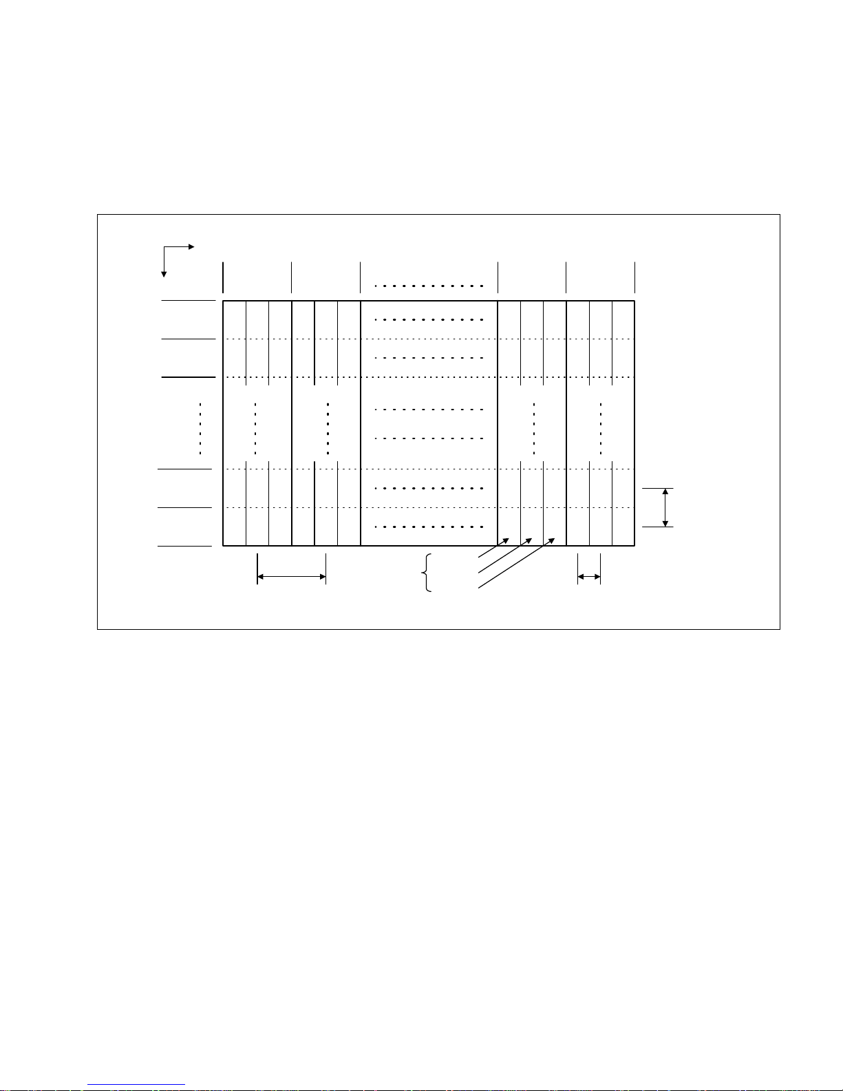
2.2.1.1 PIXEL (CELL) ARRAY
PDP is constructed by sealing the xenon, which emits neon and ultraviolet rays for discharging purpose, in between the electrod es
lay on the front glass substrate and rear glass substrate.One pixel is composed of 3 RGB cells, with cell pitch of 0.304mm (1 p ixel
0.897mm) horizontally and 0.693mm vertically.The cell is arrayed in each RGB color as shown in Fig. 1. One pixel is formed by interlacing each RGB color cell.One cell size is 0.304mm horizontally and 0.693mm vertically.
Direction
Vertically
No.1
Pixel line
No.2
Pixel line
No.767
Pixel line
No.768
Pixel line
Horizontally
No.1
Pixel
sequence
B G R B G R
BG
B
B
0.912mm(Horizontally)
RBGR
G RBG R
GRBGR
Pixel pitch
No.2
Pixel
sequence
1 pixel
(1 dot)
B
G
R
Cell
Cell
Cell
No.1023
Pixel
sequence
No.1024
Pixel
sequence
B GRBG R
BGRBGR
G RBG R
B
GRBGR
B
0.304mm(Vertically)
Cell pitch
0.693mm
(Verticall)
Pixel pitch
(Cell pitch)
Fig.1 Alignment of pixel (cell)
2.2.1.2 PIXEL FAULT
There are three pixel faults - bright fault , dark fault and flicker fault - that are respectively defined as follows.
(1) BRIGHT FAULT
In this pixel fault, a cell that should not light originally is lighting on and off.
For checking this pixel fault, input ALL BLACK SCREEN and find out the cell that is lighting on and off.
(2) DARK FAULT
In this pixel fault, a cell that should light originally is not lighting or lighting with the brightness twice as brighter as originally lighting.
For checking this pixel fault, input 100% of each R/G/B colour and find out the cell that is not lighting.
(3) FLICKER FAULT
In the pixel fault, a cell that should light originally or not light originally is flashing on and off.
For checking this pixel fault, input ALL BLACK SCREEN signal or 100% of each RGB colour and find out the cell that is flashing on
and off.
(No.52169)1-7
Page 8

2.2.2 MAIN MI-COM FUNCTIONAL TABLE [RECEIVER UNIT]
Pin No. Terminal name Port name I/O Function
1 BS-RxD SBO0 O PDP communication
2 /MICON_V /VSYNC I Vertical sync for OSD
3 LB_PRO P84 I Low B protection detect [Detection : H]
4 NC NC - Not used
5 /RST /RST I Reset for CPU [Reset : L]
6 CONV.BUSY P52 IRQ4 I Not used
7 /TEST /TEST I 3.3V
8 OSD_YS YS O OSD Ys
9 /DPCRST P83 O Not used
10 BS/D P50 O Not used
11 A_MU P82 O Audio muting [Muting: H]
12 /MICON_H /HSYNC I Horizontal sync for OSD
13 M_MU P81 O Not used
14 P46.OSDXI P46 OSDXI - Not used
15 P45.OSDXO P45 OSDXO - Not used
16 SDA2 P44 I/O Not used
17 AC_IN TM5IOB I AC power supply (60Hz)
18 SCL2 P42 O Not used
19 TU_POW P41 O Tuner power control [ON : L]
20 VCOI VCOI I LPF input
21 PDO PDO O LPF output
22 /IP_RESET P80 O Reset (L) [Reset : L]
23 OSD_YM DAYMOUT O OSD YM
24 OSD_B DABOUT O OSD B
25 POW_LED P77 O Lighting for power [Lighting : H]
26 OSD_G DAGOUT O OSD G
27 OSD_R DAROUT O OSD R
28 VREF VREF I Not used
29 IP_ERR P76 I AMDP program load
30 IREF IREF I Not used
31 COMP COMP I Not used
32 AVDD AVDD I 3.3V
33 CLL CLL O Not used
34 VREFLS VREFLS I Standard voltage (For SUB CCD)
35 SUB_CCD CVBS1 I Not used
36 NC NC - Not used
37 VSS VSS I GND
38 MAIN_CCD CVBS0 I Not used
39 VREFHS VREFHS I Standard voltage (For MAIN CCD)
40 CLH CLH I Not used
41 VDD/VPP VDD(VPP) I 3.3V
42 CLKSW1 P75 O IP clock switch [ON : L]
43 CLKSW2 P74 O IP clock switch [ON : L]
44 ON_TIM P27 O Not used
45 PDP-Rx SBO1 O PDP communication
1-8 (No.52169)
Page 9

Pin No. Terminal name Port name I/O Function
46 PDP-Tx P25 SBD1 I PDP communication
47 SBT1 SBT1 I Port for writing on board
48 NC P23 I Not used
49 NC P22 O Not used
50 SRQ P21 O Not used
51 BS1.5CTL P20 O Not used
52 /DVI_RST PWM2 O Not used
53 DVI_HP PWM1 O DVI Connection detect [Connect : H]
54 /MDR_CON PWM0 O Panel connection detect [Connect : L]
55 /BS_POW P73 O Not used
56 BS_CLK_SEL P14 O Not used
57 TU2_AID ADIN8 I Not used
58 /LOB_POW P72 O LOW B power control
59 /COMPULINK /IRQ3 I Not used
60 /POWERGOOD /IRQ2 I Power condition check [ON : L]
61 MECHA_SW P10/IRQ1 I Discontinuation of mechanical swtich detection [Pussing : L]
62 /MAIN_POW P71 O Main power control [ON : L]
63 NC NC - Not used
64 /B1_POW P70 O Not used
65 C/N ADIN4 I Not used
66 X_RAY ADIN3 I Not used
67 EE_CDS ADIN2 I Not used
68 KEY2 ADIN1 I Key scan data [ON : H]
69 KEY1 ADIN0 I Key scan data [ON : H]
2
70 SCL1 SCL1 O I
71 SDA1 SDA1 I/O I
C bus clock (For Main memory)
2
C bus data (For Main memory)
72 REMO RMIN/IRQ0 I Remote control data
73 NC P87 O Not used
74 VSS VSS I GND
75 OSC2 OSC2 O 4MHz oscillation for system clock
76 OSC1 OSC1 I 4MHz oscillation for system clock
77 VDD VDD I 3.3V
2
78 SCL0 SCL0 O I
C bus clock (for general)
79 NC P86 O Not used
2
80 SDA0 SDA0 I/O I
81 DVI_SDA P57SBT0 O I
C bus data (for general)
2
C bus data (for digital input)
82 NC P56SBD0 I Not used
83 NC NC - Not used
84 P_MU P85 O Picture muting [Muting : H]
(No.52169)1-9
Page 10

SECTION 3
DISASSEMBLY
3.1 DISASSEMBLY PROCEDURE (DISPLLAY UNIT)
• Prior to assembly/disassembly procedure of the set, be sure to
disconnect the power cord from the wall outlet.
• Perform the following procedures on a flat and strong place.
3.1.1 REMOVING THE REAR COVER (Fig.1)
(1) Remove the 9 screws [ A ] .
(2) Remove the 12 screws [ B ].
(3) Take out the REAR COVER.
B
SIDE SPEAKER
COVER
H
SHIELD COVER
3.1.2 REMOVING THE SIDE SPEAKER COVER (Fig.1)
(1) Remove the 4 screws [ C ].
(2) Take out the SIDE SPEAKER COVER.
(3) Remove the other hand SIDE SPEAKER COVER same
steps.
A
REAR COVER
I
J
C
TERMINAL
BRACKET
DISPLAY SW PWB
X
T
C
E
DISPLAY SW
ASS'Y
SIDE SPEAKER
COVER
TOP
D
DD
SPEAKER
ASS'Y
Fig.2
G
SENSOR PWB
F
1-10 (No.52169)
Fig.1
Page 11

3.1.3 REMOVING THE DD SPEAKER ASS'Y (Fig.1, Fig.2)
NOTE:
Please do not disassembly DD SPEAKER ASS'Y. A performance
may be influenced if it disassembly.
• Remove the SIDE SPEAKER COVER.
(1) Remove the 2 screws [ D ].
(2) Take out the DD SPEAKER ASS'Y.
(3) Remove the other hand DD SPEAKER ASS'Y same steps.
(4) If necessary, remove the [SR
] and [SL] connector.
3.1.4 REMOVING THE DISPLAY SW ASS'Y (Fig.1)
• Remove the SIDE SPEAKER COVER.
(1) Remove the 2 screws [ E ].
(2) Take out the DISPLAY SW ASS'Y.
3.1.5 REMOVING THE DISPLAY SW PWB (Fig.1)
• Remove the SIDE SPEAKER COVER.
• Remove the DISPLAY SW ASS'Y.
(1) Remove the 3 screws [ F ].
(2) Take out the DISPLAY SW PWB.
(3) Remove the [ T
] connector on the DISPLAY SW PWB.
3.1.6 REMOVING THE SENSOR PWB (Fig.1)
• Remove the SIDE SPEAKER COVER.
(1) Remove the 2 screws [ G ].
(2) Take out the SENSOR PWB.
(3) Remove the [ X
] connector on the SENSOR PWB.
3.1.7 REMOVING THE SHIELD COVER (Fig.1)
• Remove the REAR COVER.
(1) Remove the 6 screws [ H ].
(2) Take out the SHIELD COVER.
3.1.8 REMOVING THE TERMINAL BRACKET (Fig.1)
• Remove the REAR COVER.
• Remove the SHIELD COVER.
(1) Remove the 5 screws [ I ].
(2) Remove the 2 screws [ J ].
(3) Take out the TERMINAL BRACKET.
3.1.9 REMOVING THE LINE FILTER PWB (Fig.2)
• Remove the REAR COVER.
• Remove the SHIELD COVER.
• Remove the TERMINAL BRACKET.
(1) Remove the [ CN8001
] ( AC IN ) connector on the SMPS
PWB.
(2) Remove the 1 screw [ K ] attaching the earth wire ( black )
on the PDP UNIT.
(3) Remove the 1 screw [ L ] attachin g the earth wire ( green
and yellow ).
(4) Remove the 2 screws [ M ] .
(5) Take out the LINE FILTER PWB.
3.1.10 REMOVING THE AUDIO PWB (Fig.2)
• Remove the REAR COVER.
• Remove the SHIELD COVER.
• Remove the TERMINAL BRACKET.
(1) Remove the [ SR
], [ SL ], [ CB ] connector on the AUDIO
PWB.
(2) Remove the [ A
], [ C ], [ D ] connector on the DISPLAY
INTERFACE PWB.
(3) Remove the [ CN9003
] ( B ) connector on the VIDEO
SMPS PWB.
(4) Remove the 4 screws [ N ].
(5) Take out the AUDIO PWB.
3.1.11 REMOVING THE DISPLAY INTERFACE PWB (Fig.2)
• Remove the REAR COVER.
• Remove the SHIELD COVER.
• Remove the TERMINAL BRACKET.
(1) Remove the [ A
], [ C ], [ D ], [ E ], [ T ], [ X ], [ V ], [ G ],
[ LVDS ] connector on the DISPLAY INTERFACE PWB.
(2) Remove the 2 screws [ O ] attaching the MDR connector.
(3) Remove the 2 screws [ P ] attaching the DVI
connector.
(4) Remove the 2 screws [ Q ].
(5) Take out the DISPLAY INTERFACE PWB.
INSULATOR
LINE FILTER
PWB
M
SMPS PWB
EARTH WIRE
(GREEN &YELLOW)
CN8001
K
EARTH
WIRE
(BLACK)
CN9003
L
AUDIO PWB
N
B
A
VIDEO SMPS PWB
Fig.2
Q
V D
C2
DISPLAY
INTERFACE
PWB
A
SL
CB
SR
D
C
X
T
O
P
GE
LVDS
C
C1
MDR
DVI
(No.52169)1-11
Page 12

3.1.12 REMOVING THE CHASSIS BASE (Fig.3)
• Remove the REAR COVER.
• Remove the SHIELD COVER.
• Remove the TERMINAL BRACKET.
• Remove the LINE FILTER PWB.
• Remove the AUDIO PWB.
• Remove the DISPLAY INTERFACE PWB.
(1) Remove the 2 screws [ R ].
(2) Remove the 1 screw [ S ] attaching the earth wire.
(3) If necessary, remove the cable and wires from wire clamp.
(4) Pull up the CHASSIS BASE.
3.1.13 REMOVING THE BACK FRAME BRACKET (Fig.3)
• Remove the REAR COVER.
• Remove the SHIELD COVER.
• Remove the TERMINAL BRACKET.
• Remove the LINE FILTER PWB.
• Remove the AUDIO PWB.
• Remove the DISPLAY INTERFACE PWB.
• Remove the CHASSIS BASE.
(1) Remove the 4 screws [ T ].
(2) Remove the 4 screws [ U ].
(3) If necessary, remove the cable and wires from wire clamp.
(4) Pull up the BACK FRAME BRACKET.
(5) The other hand BACK FRAME BRACKET is removed
same steps.
3.1.14 REMOVING THE TEMP. SENSOR PWB (Fig.3)
• Remove the REAR COVER.
(1) Remove the [ V
] connector on the TEMP. SENSOR PWB.
(2) Remove the screw [ V ].
(3) Take out the TEMP. SENSOR PWB.
3.1.15 REMOVING THE PDP UNIT (Fig.3)
• Remove the REAR COVER.
• Remove the SHIELD COVER.
• Remove the TERMINAL BRACKET.
• Remove the LINE FILTER PWB.
• Remove the AUDIO PWB.
• Remove the DISPLAY INTERFACE PWB.
• Remove the CHASSIS BASE.
• Remove the BACK FRAME BRACKET.
• Remove the TEMP. SENSOR PWB.
(1) Rise with the back frame spacer on the PDP UNIT back
side.
(2) Take out the PDP UNIT.
3.1.16 REMOVING THE WOOFER SPEAKER BOX (Fig.3)
(1) Remove the 6 screws [ W ].
(2) Take out the WOOFER SPEAKER BOX.
3.1.17 REMOVING THE SPEAKER (WOOFER) (Fig.3)
• Remove the WOOFER SPEAKER BOX.
(1) Remove the 20 screws [ X ].
(2) Pull up the WOOFER SPEAKER HOLDER.
(3) Remove the 4 screws [ Y ].
(4) Take out the WOOFER.
(5) Remove the other hand WOOFER same steps.
R
U
BACK FRAME
BRACKET
T
BACK FRAME
SPACER
V
V
S
CHASSIS BASE
EARTH
WIRE
T
T
WOOFER
SPEAKER
HOLDER
U
BACK FRAME
BRACKET
W
X
T
Y
SPEAKER
(WOOFER )
WOOFER
SPEAKER
BOX
WOOFER SPEAKER
BACK COVER
TEMP. SENSOR
PWB
TOP
1-12 (No.52169)
PDP UNIT
Fig.3
Page 13

3.1.18 THE SIDE BLACKET (Fig.4)
• Remove the REAR COVER.
• Remove the SHIELD COVER.
• Remove the TERMINAL BRACKET.
• Remove the LINE FILTER PWB.
• Remove the AUDIO PWB.
• Remove the DISPLAY INTERFACE PWB.
• Remove the CHASSIS BASE.
• Remove the BACK FRAME BRACKET.
• Remove the PDP UNIT.
(1) Remove the 2 screws [ Z ].
(2) Remove the screw [ a ].
(3) Remove the screw [ b ] attaching the earth wire.
(4) Pull up the SIDE BRACKET.
(5) Remove the other hand SIDE BRACKET same steps.
Z
a
3.1.19 REMOVE THE FRONT FILTER (Fig.4)
• Remove the REAR COVER.
• Remove the SHIELD COVER.
• Remove the TERMINAL BRACKET.
• Remove the LINE FILTER PWB.
• Remove the AUDIO PWB.
• Remove the DISPLAY INTERFACE PWB.
• Remove the CHASSIS BASE.
• Remove the BACK FRAME BRACKET.
• Remove the PDP UNIT.
(1) Remove the 2 screws [ c ] attaching the UPPER
BRACKET.
(2) Remove the 6 screws [ d ] attaching the GLASS HOLDER
(UPPER) from upper side.
(3) Pull up the UPPER BRACKET.
(4) Remove the 2 screws [ e ] attaching the UPPER
BRACKET.
(5) Remove the 6 screws [ f ] attaching the GLASS HOLDER
(UPPER) from under side.
(6) Take out the FRONT FILTER .
PDP UNIT
SIDE BRACKET
MOUNTING
BOSS
UPPER
BRACKET
GLASS HOLDER
(UPPER)
TOP
GLASS HOLDER
(UNDER)
e
UNDER
BRACKET
c
EARTH
WIRE
a
d
FRONT PANEL
SIDE BRACKET
f
Z
b
FRONT FILTER
Fig.4
(No.52169)1-13
Page 14

3.1.20 DISASSEMBLY PDP UNIT UNIT (Fig.5)
3.1.20.1 REMOVING THE SMPS PWB
• Remove the REAR COVER.
(1) Remove the CN8007
CN8003
/CN8009/CN8002 connectors on the SMPS PWB.
/CN8008/CN8004/CN8005/CN8006/
(2) Remove the 8 screws [ g ].
(3) Remove the SMPS PWB.
3.1.20.2 REMOVING THE X-MAIN PWB
• Removing the REAR COVER.
(1) Remove the CN4001
/CN4002/CN4003/CN4004/CN4005
connectors on the X-MAIN PWB.
(2) Remove the 8 screws [ h ].
(3) Remove the X-MAIN PWB.
3.1.20.3 REMOVING THE Y-BUF-U PWB
• Remove the REAR COVER.
(1) Remove the CN5401
/CN5402/CN5403/CN5404/CN5405/
CN5407 connectors on the Y-BUF-U PWB.
(2) Remove the 5 screws [ i ].
(3) Lift the Y-BUF-U PWB slightly, and remove th e CN5404
CN5405 connectors on the Y-BUF-U PWB.
(4) Remove the Y-BUF-U PWB.
3.1.20.4 REMOVING THE Y-BUF-L PWB
• Remove the REAR COVER.
(1) Remove the CN5501
CN5507
connectors on the Y-BUF-L PWB.
/CN5502/CN5503/CN5504/CN5505/
(2) Remove the 5 screws [ j ].
(3) Lift the Y-BUF-L PWB slightly, and remove the CN5504/
CN5505
connectors on the Y-BUF-L PWB.
(4) Remove the Y-BUF-L PWB.
3.1.20.5 REMOVING THE Y-MAIN PWB
• Remove the REAR COVER.
• Remove the CHASSIS BASE.
• Remove the Y-BUF-U PWB.
• Remove the Y-BUF-L PWB.
(1) Remove the CN5001
/CN5008 connectors on the Y-MAIN
PWB.
(2) Remove the 7 screws [ k ].
(3) Remove the Y-MAIN PWB.
3.1.20.6 REMOVING THE LOGIC-MAIN PWB
• Remove the REAR COVER.
• Remove the CHASSIS BASE.
(1) Remove the CN2001
/CN2002/CN2003/CN2004/CN2005/
CN2006/CN2007/LA01 connectors on the LOGIC-MAIN
PWB.
(2) Remove the 6 screws [ l ].
(3) Remove the LOGIC-MAIN PWB.
3.1.20.7 REMOVING THE E-BUF-L PWB
• Remove the REAR COVER.
• Remove the BACK FRAME.
• Remove the CHASSIS BASE.
• Remove the SPEAKER BRACKET (left).
(1) Remove the EC1
/EC2/EC3/EC4/CN401/CN806/EF1
connectors on the E-BUF-L PWB.
(2) Remove the 5 screws [ m ].
(3) Remove the E-BUF-L PWB.
/
3.1.20.8 REMOVING THE F-BUF-L PWB
• Remove the REAR COVER.
• Remove the BACK FRAME.
• Remove the CHASSIS BASE.
(1) Remove the FC5
/FC6/FC7/FC8/CN402/FE1 connectors
on the F-BUF-L PWB.
(2) Remove thr 6 screws [ n ].
(3) Remove the F-BUF-L PWB.
3.1.20.9 REMOVING THE F-BUF-U PWB
• Remove the REAR COVER.
(1) Remove the EC1
/EC2/EC3/EC4/EF1/CN401 connectors
on the F-BUF-U PWB.
(2) Remove the 6 screws [ o ].
(3) Remove the F-BUF-U PWB.
3.1.20.10 REMOVING THE E-BUF-U PWB
• Remove the REAR COVER.
(1) Remove the FC5
/FC6/FC7/FC8/FE1/CN402/CN807
connectors on the E-BUF-U PWB.
(2) Remove the 5 screws [ p ].
(3) Remove the E-BUF-U PWB.
1-14 (No.52169)
3.1.20.11 REMOVING THE VIDEO SMPS PWB
• Remove the REAR COVER.
(1) Remove the CN9001
CN9007
connectors on the VIDEO SMPS PWB.
/CN9002/CN9004/CN9005/CN9006/
(2) Remove the 4 screws [ q ].
(3) Remove the VIDEO SMPS PWB.
Page 15

CN5404
CN5407
CN5405
CN5505
CN5507
CN5504
FC6
FC7
FC8
CN5008
CN5001
CN5401
CN5402
CN5403
CN5501
CN5502
CN5503
CN9005
CN9007
CN9006
CN9003
CN9002
CN9001
CN9004
CN807
CN402
CN8003
CN8005
CN8006
CN8004
FC5
CN8007
FE1
CN8008
EF1
EC4
EC3
CN401
CN8009
CN8002
CN8001
LA01
CN2005
CN2001
CN2004
CN2007
CN2006
EC1
EC2
CN2002
CN2003
CN4001
CN4003
CN4004
CN4002
CN4005
Y-BUF-U PWB
Y-BUF-L PWB
Y-MAIN PWB
i
j
EC1
p
EC2 EC3 EC4
CN806 CN401 CN402
VIDEO SMPS PWB
qk
EF1
FE1
E-BUF-U PWB F-BUF-U PWB
SMPS PWB
FC5
FC6
FC7 FC8
ohlg
X-MAIN PWB
m n
E-BUF-L PWB
LOGIC-MAIN PWB
F-BUF-L PWB
Fig.5
(No.52169)1-15
Page 16

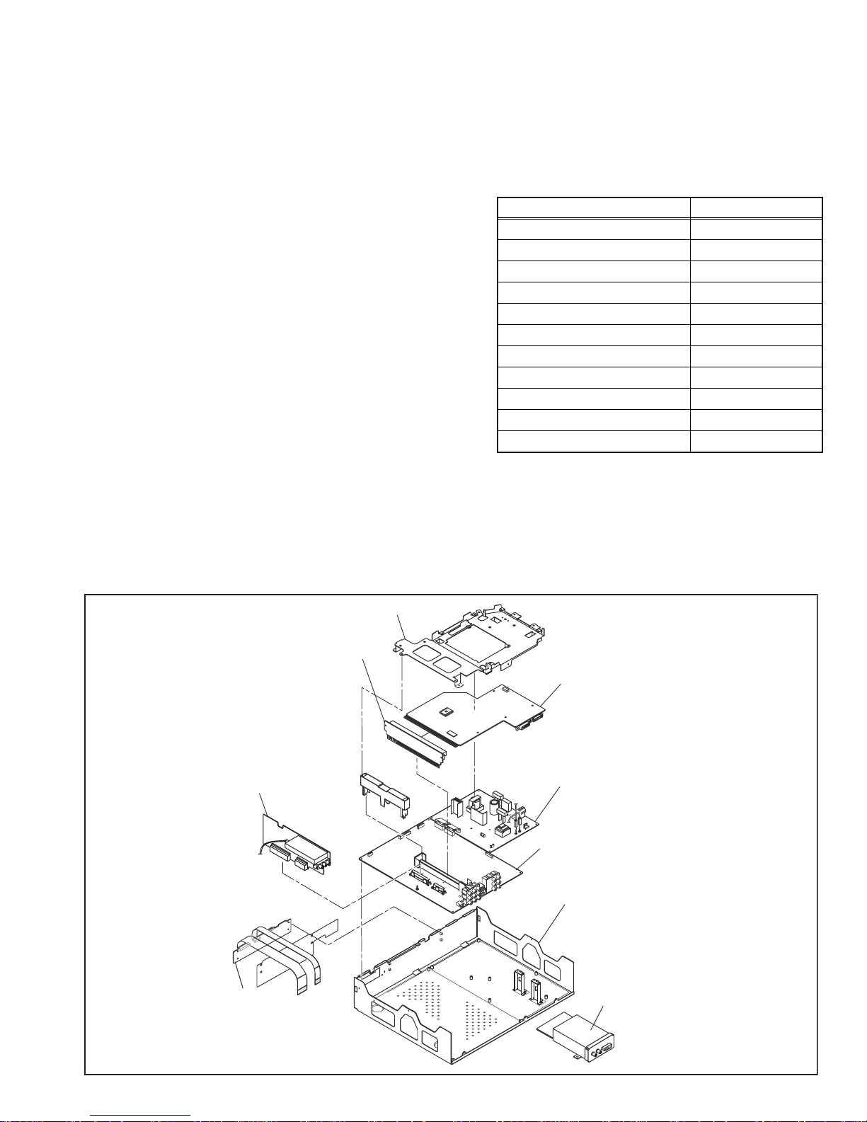
3.2 DISASSEMBLY PROCEDURE (RECEIVER UNIT) (Fig. 6)
• Make sure that the power cord is pulled out from the AC wall
socket.
3.2.1 REMOVING THE TOP COVER
(1) Remove the 4 screws [ A ] from both side of the TOP
COVER.
(2) Remove the 3 screws [ B ] from rear side of the TOP
COVER.
(3) Pull up the TOP COVER.
3.2.2 REMOVING THE BACK COVER
• Remove the TOP COVER.
(1) Remove the 2 screws [ C ] attaching the AC connector.
(2) Remove the 3 screws [ D ].
(3) Remove the 6 screws [ E ] attaching the each jacks.
(4) Remove the 2 screws [ F ] attaching the digital connector.
(5) Remove the 2 screws [ G ] attaching the DIGITAL INPUT
MODULE.
(6) Remove the 2 screws [ H ] attaching the DVI terminal.
(7) Remove the 1 nat [ I ] attaching the antenna terminal.
(8) Take out the rear cover.
3.2.3 REMOVING THE CHASSIS BRACKET
• Remove the TOP COVER.
(1) Remove the 2 screws [ J ].
(2) Pull up the CHASSIS BRACKET.
3.2.4 REMOVING THE DIGITAL INPUT MODULE
• Remove the TOP COVER.
• Remove the BACK COVER.
(1) Remove the connector [ AU
], [ SR ], [ DC ], [ Q ] on the
DIGITAL INPUT MODULE.
(2) Remove the 2 screws [ K ].
(3) Take out the DIGITAL INPUT MODULE.
3.2.5 REMOVI NG THE MI-COM & DIST MODULE PWB AN D
DIST RELAY PWB
• Remove the TOP COVER.
• Remove the BACK COVER.
• Remove the DIGITAL INPUT MODULE.
(1) Remove the [ CN100A
] connector on the MI-COM & DIST
MODULE PWB.
(2) Remove the 2 screws [ L ].
(3) Remove the 2 screws [ M ].
(4) Remove the 2 screws [ N ].
(5) Pull up the DIST RELAY PWB from MAIN PWB.
(6) Remove the 5 screws [ O ] attaching the MI-COM & DIST
MODULE PWB.
(7) Take out the MI-COM & DIST MODULE PWB and DIST
RELAY PWB from the DIST HOLDER.
3.2.6 REMOVING THE RECEIVER POWER PWB
• Remove the TOP COVER.
• Remove the BACK COVER.
• Remove the DIGITAL INPUT MODULE.
• Remove the MI-COM & DIST MODULE PWB and DIST
RELAY PWB.
(1) Remove the [ CN1001
] and [ CN1002 ] connector on the
MAIN PWB.
(2) Remove the [ CN90PW
] [ CN900X ] and [ CN90E1 ]
connector on the RECEIVER POWER PWB.
(3) Remove the earth wire [ CN90E2 ] from chassis.
(4) Remove the 6 screws [ P ].
(5) Take out the RECEIVER POWER PWB.
3.2.7 REMOVING THE FRONT PANEL
• Remove the TOP COVER.
(1) Remove the 1 screw [ Q ] from front side.
(2) Remove the 1 screw [ R ] from top side.
(3) Remove the 2 claws [ Y ] from left and right side.
(4) Pull out the FRONT PANEL.
3.2.8 REMOVING THE DAMPER
• Remove the TOP COVER.
• Remove the FRONT PANEL.
(1) Remove the 1 screw [ S ] from back side of the FRONT PANEL.
(2) Remove the DAMPER.
3.2.9 REMOVING THE FRONT CONTROL PWB
• Remove the TOP COVER.
• Remove the FRONT PANEL.
(1) Remove the card wire from the [ H
] and [ G ] connector.
(2) Remove the 4 screws [ T ].
(3) Take out the FRONT CONTROL PWB.
3.2.10 REMOVING THE RECEIVER PWB
• Remove the TOP COVER.
• Remove the BACK COVER.
• Remove the CHASSIS BRACKET.
• Remove the DIGITAL INPUT MODULE.
• Remove the MI-COM & DIST MODULE PWB and DIST RELAY PWB.
(1) Remove the [ CN1005
] and [ CN1006 ] connector.
(2) Pull up the RECEIVER PWB.
3.2.11 REMOVING THE MAIN PWB
• Remove the TOP COVER.
• Remove the BACK COVER.
• Remove the CHASSIS BRACKET.
• Remove the DIGITAL INPUT MODULE.
• Remove the MI-COM & DIST MODULE PWB and DIST RELAY PWB.
• Remove the FRONT PANEL.
• Remove the RECEIVER PWB.
(1) Remove the 3 screws [ U ] attaching the bracket.
(2) Remove the 2 screws [ V ].
(3) Remove the 2 screws [ W ].
(4) Take out the MAIN PWB.
DIGITAL INPUT MODULE
1
3
5
BACK COVER
SB
connector
1-16 (No.52169)
CAUTION AT DISASSEMBLY
Prior to disassembly, unplug the power code from the AC outlet without fail. (Turn
the power "off".)
Short the SB connector [1] pin and [2] pin of the DIGITAL INPUT MODULE. (At the
time of assembling)
Before the rear panel is inserted into the cabinet, release the short-circuit between
2
4
6
the SB connector [1] pin and [2] pin of the DIGITAL INPUT MODULE.
After releasing the short-circuit between the SB connectors, do not turn the power
on until the rear panel is inserted into the cabinet.
Negligence in carrying out the above steps may cause the inactivation of the TV.
Page 17

TOP COVER
A
(x4)
A
CHASSIS BRACKET
J
(x2)
FRONT
PANEL
Q
Y
Claw
a
FRONT PANEL
(BACK SIDE)
DAMPER
R
(x1)
B
(x3)
M
N
(x2)
J
(x2)
L
(x2)
DIST HOLDER
CN100A
DIST RELAY PWB
b
MI-COM & DIST
MODULE PWB
RECEIVER PWB
O
(x5)
S
c
CN1006
Y
Claw
H
T
(x4)
CN1005
(x2)
CN1001
CN1002
V
G
P
(x6)
RECEIVER POWER PWB
g
CN90PW
CN90E1
CN90E2
CN900X
MAIN PWB
FRONT
DOOR
FRONT
CONTROL
PWB
FFC WIRE
U
(x2)
FRONT PANEL
e
e
d
BRACKET
Fig.6
(x2)
d
a
ANTENNA
TERMINAL
W
DC
AU
DIGITAL INPUT
MODULE PWB
c
BACK COVER
BOTTOM CASE
b
C
g
SR
Q
EARTH WIRE
CN90E2
K
(x2)
AC
INLET
F
(x2)
D
(x3)
G
H
(x2)
(x2)
I
E
(x6)
(No.52169)1-17
Page 18

3.3 REPLACEMENT OF MEMORY IC
MAIN MENU
This unit uses the nonvolatile memory IC. The memory IC memories data for video-chroma and drive circuits. To replace the memory
IC without the data written, malfunctions might occurred while power is on, and the normal image might not appear. Wh en replaci ng
the memory IC, be sure to use the IC written with the initial values of data.
3.3.1 PROCEDURE FOR REPLACING THE MEMORY IC
NOTE:
Before entering the SERVICE MODE, confirm that the setting
of TV / CATV SW of the REMOTE CONTROL UNIT is at the
"TV" side and the setting of VCR / DVD SW is at the "VCR"
side. If the switches have not been properly set, you cannot
enter the SERVICE MODE.
(1) Switch the power off and unplug the power cord from the
wall outlet.
(2) Replacing the memory IC. [Be sure to use the IC written
with the initial values of data]
(3) Plug the power cord into the wall outlet and switch the
power on.
(4) Receive channel setting
(5) User setting
Memories the user setting items. The [SETTINGS OF
FACTORY SHIPMENT] setting is as next page.
(6) SERVICE MODE
Check the SERVICE MODE setting items of setting mode
in Table 1, set if necessary. For setting method, please
refer to the [ADJUSTMENT PREPARATION :
ADJUSTMENT PROCEDURE ] of ADJUSTMENT section.
MAIN MENU
1.PICTURE/SOUND
2.YC SEP
3.WHITE BALANCE
4.MEMORY SETUP
7.PANEL
8.PP
9.IP
0.HDMI
5.RF AFC
6.DD/CM
1. PICTURE/SOUND (sound and picture setting)
Sound circuits (A) Fixed A01~A27
Video circuits (S) Adjust S01~S99
Deflection circuits (D) Fixed D01~D32
Factory setting items (F) Adjust F01~F59
2. YC SEP
3-dimensional YC separation
setting
3. WHITE BALANCE: Cannot adjust
4. MEMORY SETUP: Do not adjust
Memory data edit Fixed -
5. RF AFC: AFC setting (Automaticaly set)
6. DD/CM
Panel image processing setting Adjust DDT01~DDT34
7. PANEL: Do not adjust
Panel power limit control Fixed PDA001~PDA012
8. PP
Multi-screen processing setting A djust ADM001~ADM034
9. IP
DIST processing setting Fixed IPA001~IPA120
0. HDMI
Digital input process setting Fixed HDM001~HDM080
SERVICE MODE SETTING ITEMS
Setting items Settings Item No.
Adjust YCM001~YCM185
Fixed YCS001~YCS114
Fixed CMT01~CMT57
Fixed DDP01~DDP37
Fixed CMP01~CMP03
Fixed PDB001~PDA021
Fixed RGA001~RGA003
Fixed PPA001~PPA008
Fixed PPB001~PPB036
Fixed PPC001~PPC008
Fixed PPD001~PPD025
Fixed IPB001~IPB079
Fixed IPC001~IPC044
Fixed IPD001~IPD026
Fixed IPE001~IPE015
Fixed RHD001~RHD170
1-18 (No.52169)
Page 19
3.3.2 SETTINGS OF FACTORY SHIPMENT
3.3.2.1 BUTTON OPERATION (DISPLAY UNIT) 3.3.2.2 REMOTE CONTROL DIRECT OPERATION
Setting item Setting value
INPUT TV
CHANNEL 1
VOLUME 10
INPUT TV
CHANNEL CABLE-02
VOLUME 10
Setting item Setting value
MUTING OFF
DISPLAY OFF
SOUND AHS OFF
BBE ON
AHB ON
ASPECT PANORAMA
OFF TIMER OFF
VIDEO STATUS DINAMIC
NATURAL CINEMA AUTO
3.3.2.3 REMOTE CONTROL MENU OPERATION
(1) PICTURE ADJUSTMENT
Customers can adjust the picture setting of menu screen as their own like but the picture standard value during factory shipment is as
below.
NTSC MODE
PICTURE BRIGHT COLOR TINT DETAIL
COLOR
TEMPERATURE
DIG. NOISE
CLEAR
COLOR
MANAGEMENT
DINAMIC +04 -03 +08 00 +06 HIGH OFF VIVID
STANDARD 00 00 00 00 00 LOW OFF VIVID
GAME -05 00 -03 00 -03 HIGH OFF VIVID
THEATER 00 00 00 00 00 HIGH OFF VIVID
HD MODE
PICTURE BRIGHT COLOR TINT DETAIL
COLOR
TEMPERATURE
DIG. NOISE
CLEAR
COLOR
MANAGEMENT
DINAMIC +05 -02 -08 00 +05 HIGH OFF VIVID
STANDARD 00 00 00 00 00 LOW OFF VIVID
GAME -05 00 +03 00 -03 HIGH OFF VIVID
THEATER 00 00 00 00 00 LOW OFF VIVID
(2) SOUND
Setting item Setting value
TREBLE 00
BASS 00
BALANCE 00
MTS STREO
(3) SETTINGS
Setting item Setting value Setting item Setting value
POSITION ADJUSTMENT Center NOISE MUTING ON
VIDEO STATUS DYNAMIC FRONT PANEL LOCK OFF
XDS ID ON AUTO SHUT OFF OFF
POWER INDICATOR HIGH DIGITAL-IN SIZE-1
TV SPEAKER OFF ON V-CHIP OFF
AUDIO OUTPUT FIX AUTO DEMO OFF
LANGUAGE ENG IMAGE SHIFT STD
CLOSED CAPTION OFF V1 SMART INPUT OFF
(No.52169)1-19
Page 20

3.4 REPLACEMENT OF CHIP COMPONENT
3.4.1 CAUTIONS
(1) Avoid heating for more than 3 seconds.
(2) Do not rub the electrodes and the resist parts of the pattern.
(3) When removing a chip part, melt the solder adequately.
(4) Do not reuse a chip part after removing it.
3.4.2 SOLDERING IRON
(1) Use a high insulation soldering iron with a thin pointed end of it.
(2) A 30w soldering iron is recommended for ea sily removing parts.
3.4.3 REPLACEMENT STEPS
1. How to remove Chip parts
2. How to install Chip parts
[Resistors, capacitors, etc.]
(1) As shown in the figure, push the part with tweezers and al-
ternately melt the solder at each end.
(2) Shift with the tweezers and remove the chip part.
[Transistors, diodes, variable resistors, etc.]
(1) Apply extra solder to each lead.
SOLDER
SOLDER
[Resistors, capacitors, etc.]
(1) Apply solder to the pattern as indicated in the figure.
(2) Grasp the chip part with tweezers and place it on the sol-
der. Then heat and melt the solder at both ends of the chip
part.
[Transistors, diodes, variable resistors, etc.]
(1) Apply solder to the pattern as indicated in the figure.
(2) Grasp the chip part with tweezers and place it on the sol-
der.
(3) First solder lead A as indicated in the figure.
(2) As shown in the figure, push the part with tweezers and al-
ternately melt the solder at each lead. Shift and remove the
chip part.
NOTE :
After removing the part, remove remaining solder from the pattern.
1-20 (No.52169)
A
B
C
(4) Then solder leads B and C.
A
B
C
Page 21
SECTION 4
ADJUSTMENTS
4.1 ADJUSTMENT PREPARATION
(1) There are 2 ways of adjusting this TV : One is with the
REMOTE CONTROL UNIT and the other is the
conventional method using adjustment parts and
components.
(2) The adjustment using the REMOTE CONTROL UNIT is
made on the basis of the initial setting values. The
setting values which adjust the screen to the optimum
condition can be different from the initial setting
values.
(3) Make sure that connection is correctly made AC to AC
power source.
(4) Turn on the power of the TV and measuring instruments for
warning up for at least 30 minutes before starting
adjustments.
(5) If the receive or input signal is not specified, use the mo st
appropriate signal for adjustment.
(6) Never touch the parts (such as variable resistors,
transformers and condensers) not shown in the adjustment
items of this service adjustment.
4.2 MEASURING INSTRUMENT AND FIXTURES
• DC voltmeter (or Digital voltmeter)
• Oscilloscope
• Signal generator (Pattern generator)
• Remote control unit
(7) Preparation for adju stment. Unless otherwise specified in
the adjustment items, preset the following functions with
the REMOTE CONTROL UNIT.
Setting item Settings
VIDEO STATUS STANDARD
BRIGHT / CONTRAST / COLOR / TINT
Center
COLOR TEMPERATURE LOW
DIG. NOISE CLEAR OFF
COLOR MANEGMENT STD
NATURAL CINEMA OFF
DIGITAL VNR OFF
TREBLE / BASS / BALANCE Center
BBE OFF
AHS OFF
AHB OFF
4.3 MAIN PARTS LOCATIONS (RECEIVER UNIT)
DIST RELAY PWB
RECEIVER PWB
DIST HOLDER
MI-COM & DIST MODULE PWB
RECEIVER POWER PWB
MAIN PWB
BOTTOM CASE
FRONT CONTROL PWB
DIGITAL INPUT MODULE
(No.52169)1-21
Page 22

4.4 MAIN PARTS LOCATIONS (DISPLAY UNIT)
DISPLAT SW
PWB
T
LINE FILTER PWB
SENSOR PWB
B
X
DD SPEAKERDD SPEAKER
SL
CN9001 (PDP UNIT : VIDEO SMPS PWB)
V
TEMP. SENSOR PWB
A
WOOFER
AUDIO PWB
SR CB
D
C
D
V
A
X
C
T
CN9002 (PDP UNIT : VIDEO SMPS PWB)
Q E
CN9001 (PDP UNIT : SMPS PWB)
1-22 (No.52169)
LVDS
DISPLAY INTERFACE PWB
LA01 (PDP UNIT : LOGIC-MAIN PWB)
Page 23

4.5 SERVICE MENU SCREEN
VOLUME(+/-) key
CHANNEL(+/-) key
MAIN MENU
1.PICTURE/SOUND
2.YC SEP
3.WHITE BALANCE
4.MEMORY SETUP
5.RF AFC
6.DD/CM
1.PICTURE/SOUND
NTSC CINE ST L FL MUTE
A01 001
7.PANEL
8.PP
9.IP
0.HDMI
4.MEMORY SETUP
ADDRESS(H) 0000
0
1
2
3
4
AA
55
00
0
1
AA
55
00
5
00
FF
00
2
3
4
5
00
FF
00
5.RF AFC
TOO HIGH GOOD TOO LOW
TUNER MAIN
AFC ON
FINE -10
6.DD/CM
NTSC CINE ST L FL MUTE
DDT01
DO NOT ADJUST
6
7
00
00
6
7
00
00
DDT01~34
CMT01~57
DDP01~37
CMP01~03
YCM001~185
YCS001~114
A01~A27
A01
S01~S99
S01
D01~D32
D01
F01~F59
F01
2.YC SEP
NTSC CINE ST L FL MUTE
YCM01
7. PANEL
PDA001
IN
APL
OUT
MIN
8.PP
NTSC CINE ST L FL MUTE
PPA001
9.IP
NTSC CINE ST L FL MUTE
IPA001
TEM
MAX
DO NOT ADJUST
PDA001~012
PDB001~022
RGA001~003
ADM001~034
PPA001~008
PPB001~036
PPC001~008
PPD001~025
DO NOT ADJUST
IPA001~120
IPB001~079
IPC001~044
IPD001~026
IPE001~015
3. WHITE BALANCE
BR
DRV R069 B054
CUT R078 G079 B079
0.HDMI
NTSC CINE ST L FL MUTE
GCR001
HDM001~080
RHD001~170
(No.52169)1-23
Page 24

4.6 BASIC OPERATION OF THE SERVICE MODE [USING REMOTE CONTROL]
MAIN MENU
4.6.1 HOW TO ENTER THE SERVICE MODE
NOTE:
Ensure that the cursor (arrow) of the User Menu screen is
pointing at Picture Control.
Before entering the SERVICE MODE, confirm that the setting
of TV / CATV SW of the REMOTE CONTROL UNIT is at the
"TV" side and the setting of VCR / DVD SW is at the "VCR"
side. If the switches have not been properly set, you cannot
enter the SERVICE MODE.
(1) Set to 0 minutes using the [SLEEP TIMER] key.
(2) Press the [VIDEO STATUS] key and [DISPLAY] key
simultaneously, then enter the Service Menu mode.
1.PICTURE/SOUND
2.YC SEP
3.WHITE BALANCE
4.MEMORY SETUP
5.RF AFC
6.DD/CM
(3) When the Main Menu is displayed, press any key of the [0]
to [9] key to enter the corresponding menu mode.
*Press any of the [0] to [9] keys before the Service Menu
mode disappears.
(4) Select the service item using the [ CH (+/-)] key.
(5) Set the value using the [ VOL. (+/-)] key.
(6) Press the [MUTING] key to memorize the set value.
4.6.2 HOW TO EXIT THE SERVICE MODE
Press the [ BACK ] key to exit the Service mode.
MAIN MENU
7.PANEL
8.PP
9.IP
0.HDMI
4.6.3 SERVICE CONTROL KEY LAYOUT ON THE REMOTE CONTROL
TV
CATV VCR DVD
TV/CATV SW
[MUTING] key
[VOL (+/-)] key
SPLIT
FREEZE
INPUT 1
INPUT 2
INPUT 3
INPUT 4
DIGITAL-IN
D-IN
SLEEP TIMER
MUTING
MENU
VCR CHANNEL
OPEN CLOSE
ASPECT
MULTI SCREEN
INDEX
SWAP SELECT
V1
123
V2
456
V3
789
100+
V4
THEATER
NATURAL
PRO
CINEMA
DISPLAY SOUND
+
CH
VOL
OK
CH
VCR DVD
PREV NEXT
POWER
REW
REC PAUSE
STOP
RM-C13G
RETURN+
0
STATUS
VOL
TV VCR
STILL PAUSE
VIDEO
LIGHT
BACK
FFPLAY
TV
C.C.
C.C.
VCR / DVD SW
[0]~[9] key
[VIDEO STATUS] key
[DISPLAY] key
[CH (+/-)] key
[BACK] key
1-24 (No.52169)
Page 25

4.6.4 SETTINGS OF THE SERVICE MENUS
4.6.4.1 [1. PICTURE/SOUND (Picture/sound setting)]
Adjusts output data to ports such as Audio, Drive, Video and
others (Item F):
(1) SIGNAL TYPE
The signal currently displayed on the screen is displayed.
NTSC : NTSC (525i = S/Composite)
DVD : 525i (Component)
ED : 525p
HD : 1125i
750p : 750p
HED1 : HDCP 525p size1
HED2 : HDCP 525p size2
HHD : HDCP 1125i
H750 : HDCP 750p
(2) ASPECT / MULTI
ONE SCREEN
FULL : FULL
PANO : PANORAMA
CINE : CINEMA
REGU : REGULER
MULTI SCREEN
M1 : SINGLE (for adjustment)
M2-1 : SPLIT (4 : 3)
M2-2 : SPLIT (16 : 9)
M4 : POP
M12 : INDEX
(3) PICTURE SELECTION
Displays current picture selection mode
ST : STANDARD
DA : DINAMIC
TH : THEATER
GA : GAME
(4) WHITE BALANCE
Displays white balance setting item in the picture selection mode
H : HIGH
L: LOW
(5) SERVICE ITEM CODES
Displays corresponding codes for A: Sound, S: Signal, D:
Deflection and F: Factory Settings.
< Settings of Service Item >
• [ CH (+/-)] key
For scrolling up/ down the item codes.
A01 S01 D01 F01
• [ SLEEP TIMER ] key
For switching to the next item.
A01 S01 D01 F01
(6) VALUE SETTING (DATA)
Specify values for each of the items in sequence.
• [ VOL (+/-)] key
For selecting the value (data) of each item by scrolling
up/down the key.
• [MUTING] key
For saving the entered values (data).
(7) DATA SAVING METHOD
Displays the method for saving the entered values (data).
MUTE : Press [MUTING] key
DIR : Change data then memory at the same time.
(8) I-P interpolation MODE
Not required in servicing.
FL : FRAME
L1 : LINE
23 : COMPULSORY NATURAL CINEMA IN
(2) Adpect / Multi
(1) Signal Type
NTSC FULL ST L FL MUTE
A01
(3) Picture Selection
(8) I-P interpolation MODE
***
(4) White Balance
(7) Data Saving Method
(6) Value Setting(Data)(5) Service Item Codes
NOTE:
Setting for any of the following items that is not included in the
“ADJUSTMENT PROCEDURE” section found in the later part
of this manual will not be performed in servicing.
4.6.4.2 [2. YC SEP (3D Y/C Separation setting)]
< Do not change settings of items that are not included in the
"ADJUSTMENT PROCEDURE" section. >
Sets output data to the 3D Y/C separation circuit.
• [ CH (+/-)] key
For scrolling up/down the item codes.
• [ VOL (+/-)] key
For scrolling up/down the data values.
4.6.4.3 [3. WHITE BALANCE (White Balance setting)]
Setting for this item is not required in servicing.
4.6.4.4 [4. MEMORY SETUP (Memory setting)]
[Do not change settings]
4.6.4.5 [5. RF AFC]
Setting for this item is not required in servicing.
4.6.4.6 [6. DD/CM]
< Do not change settings of items that are not included in the
"ADJUSTMENT PROCEDURE" section. >
Adjustment of color manegment and device driver
• [ CH (+/-)] key
For scrolling up/down the item codes.
• [ VOL (+/-)] key
For scrolling up/down the data values.
4.6.4.7 [7. PANEL]
[Do not change settings]
Panel power limit control
4.6.4.8 [8. PP (Multi-screen Processing setting)]
< Do not change settings of items that are not included in the
"ADJUSTMENT PROCEDURE" section. >
Sets output data to the multi-screen processing circuit.
• [ CH (+/-)] key
For scrolling up/down the item codes.
• [ VOL (+/-)] key
For scrolling up/down the data values.
4.6.4.9 [9. IP (DIST setting)]
[Do not change settings]
Sets output data to the DIST circuit.
4.6.4.10 [0. HDMI]
[Do not change settings]
Sets output data to the DIGITAL INPUT circuit
(No.52169)1-25
Page 26
4.7 INITIAL SETTING VALUES IN THE SERVICE MODE
• Perform fine-tuning based on the "initial values" using the remote control when in the Service mode.
• The "initial values" serve only as an indication rough standard and therefore the values with which optimal display can be achieved
may be different from the default values. But, don't change the values that are not written in "ADJUSTMENT PROCEDURE". They
are fixed values.
NOTE:
As for the items whose settings are "Fixed" in Table 1 in "3.3 REPLACEMENT OF MEMORY IC", the following tables show initial
values in NTSC signal input mode. As for the items whose conditions of SETTING VALUE are not written in the following tables,
the following tables show initial values in NTSC signal input mode.
• Among the initial values, there are some that are displayed "( )"as offset values. These are values relative to the base or absolute
values. Set the values by addinG offset values to the base values. Base values are displayed as "---".
4.7.1 [1.PICTURE/SOUND]
Item
No.
Item
Variable
range
Setting value
A01 (Not display) 000~007 003
A02 (Not display) 000~007 003
A03 (Not display) 000~007 003
A04 (Not display) 000~007 004
A05 (Not display) 000~015 009
A06 (Not display) 000~015 006
A07 (Not display) 000~015 006
A08 (Not display) 000~015 003
A09 (Not display) 000~007 006
A10 (Not display) 000~007 004
A11 (Not display) 000~063 063
A12 (Not display) 000~063 063
A13 (Not display) 000~003 000
Item
No.
Item
A15 (Not display) 000~003 000
A16 (Not display) 000~003 000
A17 (Not display) 000~003 000
A18 IN LEVEL 000~255 (Not used)
A19 LOW SEP 000~255 (Not used)
A20 HI SEP 000~255 (Not used)
A21 AHS MVE -128~+127 000
A22 AHS MSC -128~+127 000
A23 (Not display) 000~001 (Not used)
A24 (Not display) 000~001 (Not used)
A25 (Not display) 000~001 (Not used)
A26 (Not display) 000~001 (Not used)
A27 (Not display) 000~001 (Not used)
Variable
range
Setting value
A14 (Not display) 000~007 000
Item
No.
Item
Variable
range
NTSC 525i 525p 750p/1125i
STANDARD THEATER STANDARD THEATER STANDARD THEATER STANDARD THEATER
S01 COLOR 000~255 140 135 140 130 140 130 148 140
S02 TINAD 000~255 000 000 000 000 000 000 000 000
S03 OF COLOR -127~128 (---) (---) (---) (---) (---) (---) (---) (---)
S04 OF TINAD -127~128 (---) (---) (---) (---) (---) (---) (---) (---)
Setting value
Setting value
Item
No.
Item
Variable
range
NTSC 525i/525p 750p/1125i
STANDARD THEATER STANDARD THEATER STANDARD THEATER
S05 BRIG 000~ 255 038 038 044 0 40 043 038
S06 CONT 000~255 125 125 128 128 128 128
S07 OF BRIG -127~128 (---) (---) (---) (---) (---) (---)
S08 OF CONT -127~128 (---) (---) (---) (---) (---) (---)
1-26 (No.52169)
Page 27
Item
No.
Item
Variable
range
NTSC 525i 525p 750p/1125i
STANDARD THEATER STANDARD THEATER STANDARD THEATER STANDARD THEATER
S09 BYGN 000~255 126 130 125 130 128 130 118 120
S10 OF BYGN -127~128 (---) (---) (---) (---) (---) (---) (---) (---)
S11 RYAXIS -127~128 +006 000 +006 000 +006 000 000 000
S12 MTX 000~003 000 000 000 000 000 000 001 001
Setting value
Item
No.
Item
Variable
range
Setting value
S13 (Not display) --- (Not used)
S14 (Not display) --- (Not used)
S15 (Not display) --- (Not used)
S16 (Not display) --- (Not used)
S17 (Not display) --- (Not used)
S18 (Not display) --- (Not used)
Setting value
Item
No.
Item
Variable
range
NTSC 525i525p 750p/1125i
STANDARD THEATER STANDARD THEATER STANDARD THEATER
S19 CUTR 000~255 128 128 128 128 128 128
S20 OF CUTR -127~128 000 0 00 000 000 000 000
S21 CUTG 000~255 128 128 128 128 128 128
S22 OF CUTG -127~128 128 128 128 128 128 128
S23 CUTB 000~255 128 128 128 128 128 128
S24 OF CUTB -127~128 000 000 000 000 000 000
S25 CUTR 000~001 000 000 000 000 000 000
S26 CUTG 000~001 000 000 000 000 000 000
S27 CUTB 000~001 000 000 000 000 000 000
S28 BTHN 000~001 001 000 001 000 001 000
S29 BCALM 000~001 000 000 000 000 000 000
S30 BKAKOU 000~031 008 003 002 000 002 004
S31 BLIM 000~063 016 010 015 000 015 003
S32 BSTPO 000~063 048 050 050 050 055 050
S33 BKAKON 000~001 001 001 001 001 001 001
S34 WTHN 000~001 001 001 001 001 001 001
S35 WCALM 000~001 000 000 000 000 000 001
S36 WKAKOU 000~031 000 000 000 000 000 000
S37 WLIM 000~255 200 255 220 255 225 225
S38 WSTPO 000~063 050 000 054 000 018 000
S39 WPEAK 000~063 060 063 065 063 060 063
S40 WKAKON 000~001 001 000 001 000 001 000
S41 WGAINC 000~001 000 001 001 001 000 001
S42 GAINB 000~003 001 000 001 000 000 000
S43 SLIC 000~031 011 031 013 031 012 031
S44 APG 000~003 001 003 001 003 001 003
S45 GAINA 000~003 001 003 001 003 001 003
(No.52169)1-27
Page 28

Item
No.
Item
Variable
range
Setting value
STANDARD THEATER
S46 (Not used) 000~015 015 015
S47 (Not used) 000~015 015 015
Item
No.
Item
Variable
range
NTSC 525i/525p 750p/1125i
STANDARD THEATER STANDARD THEATER STANDARD TH EATER
S48 DCTRAN 000~015 015 015 015 015 015 015
Setting value
Item
No.
Item
Variable
range
SPLIT-SCREEN REGULAR
Setting value
S49 HSTR 000~001 000 000
S50 HSTR 000~255 013 019
S51 HEND 000~001 000 000
S52 HEND 000~255 076 067
S53 VSTR 000~001 000 000
S54 VSTR 000~255 005 005
S55 VEND 000~001 000 000
S56 VEND 000~255 094 094
S57 BHSTR 000~255 000 000
S58 BHSTR 000~015 000 000
S59 BHEND 000~255 013 013
S60 BHEND 000~015 000 000
Setting value
Item
No.
Item
Variable
range
NTSC 525i/525p 750p/1125i
STANDARD THEATER STANDARD THEATER STANDARD TH EATER
S61 PLPOL2 000~001 001 001 001 001 001 001
S62 PLEV2 000~127 016 016 016 016 016 016
S63 PLPOL1 000~001 000 000 000 000 000 000
S64 PLEV1 000~127 000 000 000 000 000 000
NOTE:
Data of the setting value is selected in the order of "SPLIT-SCREEN" and "REGULAR".
Item
No.
Item
Variable
range
STANDARD THEATER STANDARD THEATER STANDARD THEATER STANDARD THEATER
S65 MODC 000~003 003 003 003 003 002 002 002 002
S66 RMC 000~003 001 001 003 003 001 003 003 003
S67 RGA 000~003 003 003 003 003 002 003 003 003
S68 CLIP 000~015 000 000 000 000 000 000 000 000
S69 COR 000~063 019 019 019 019 019 019 019 019
1-28 (No.52169)
Setting value
NTSC
525i/525p 750p/1125iMULTI-SCREEN ASPECT
SPLIT REGULAR
Page 29
Item
No.
Item
Variable
range
Setting value
S70 TINTON 001~001 001
S71 DRIVER 001~255 240
S72 DRIVEG 001~255 240
S73 DRIVEB 001~255 240
S74 EECONT 001~031 006
S75 EEBRT 001~031 003
Item
No.
Item
Variable
range
NTSC 525i/525p 750/1125i
Setting value
S76 EETBRT -127~128 000 000 000
S77 EETCONT -127~128 000 000 000
Item
No.
Item
Variable
range
Setting value
STANDARD THEATER
S78 PICMAX 001~255 255 255
S79 PICMIN 001~255 000 000
S80 BRTMAX 001~255 255 255
S81 BRTMIN 001~255 000 000
S82 COLMAX 001~255 255 255
S83 COLMIN 001~255 000 000
Item
No.
Item
Variable
range
Setting value
S84 (Not display) 001~015 (Not used)
S85 (Not display) 001~255 (Not used)
S86 (Not display) 001~255 (Not used)
S87 (Not display) 001~003 (Not used)
Item
No.
Item
Variable
range
NTSC 525i 525p 750p/1125i
STANDARD THEATER STANDARD THEATER STANDARD THEATER STANDARD THEATER
S88 APLGAIN 001~007 007 007 007 007 007 007 007 007
S89 APLLIM 001~255 030 030 030 030 030 030 030 030
S90 ABSGAIN 001~127 000 000 000 000 000 000 000 000
S91 BLKGAIN 001~007 007 007 007 007 007 007 007 007
S92 BLKLIM 001~031 031 031 031 031 031 031 031 031
S93 WHTGAIN 001~007 007 007 007 007 007 007 007 007
S94 WHTLIM 001~031 031 031 031 031 031 031 031 031
S95 DCSTART 001~255 060 060 055 060 055 060 060 060
S96 DCGAIN 001~015 008 006 018 006 008 008 006 006
S97 DCLIM 001~063 030 025 025 019 025 025 030 025
S98 (Not display) 001~001 000 000 000 000 000 000 000 000
S99 (Not display) 001~001 000 000 000 000 000 000 000 000
Setting value
(No.52169)1-29
Page 30

Item
No.
Item
Variable
range
Setting value
D01 (Not display) 000~127 000
D02 (Not display) 000~063 000
D03 (Not display) 000~127 000
D04 (Not display) 000~063 000
D05 (Not display) 000~031 000
D06 (Not display) 000~127 000
D07 (Not display) 000~127 000
D08 (Not display) 000~031 000
D09 (Not display) 000~031 000
D10 (Not display) 000~007 000
D11 (Not display) 000~007 000
D12 (Not display) 000~001 000
D13 (Not display) 000~031 000
D14 (Not display) 000~031 000
D15 (Not display) 000~255 000
D16 (Not display) 000~255 000
D17 (Not display) 000~001 000
D18 (Not display) 000~015 000
D19 (Not display) 000~015 000
D20 (Not display) 000~015 000
D21 (Not display) 000~015 000
D22 (Not display) 000~001 000
D23 (Not display) 000~031 000
D24 (Not display) 000~031 000
D25 (Not display) 000~015 000
D26 (Not display) 000~015 000
D27 (Not display) 000~127 052
D28 (Not display) 000~003 000
D29 (Not display) 000~001 000
D30 (Not display) 000~001 000
D31 (Not display) 000~001 000
D32 (Not display) 000~001 000
Item
No.
Item
Variable
range
Setting value
F01 (Not display) 000~255 008
F02 (Not display) 000~255 001
F03 (Not display) 000~255 000
F04 (Not display) 000~255 032
F05 (Not display) 000~001 000
F06 (Not display) 000~001 001
F07 (Not display) 000~255 111
F08 (Not display) 000~255 039
F09 (Not display) 000~015 000
F10 (Not display) 000~015 000
F11 (Not display) 000~015 000
F12 (Not display) 000~015 000
F13 (Not display) 000~015 000
F14 (Not display) 000~015 000
F15 (Not display) 000~015 000
F16 (Not display) 000~127 070
F17 (Not display) 000~001 000
F18 (Not display) 000~001 000
F19 (Not display) 000~001 000
F20 (Not display) 000~255 005
F21 (Not display) 000~255 002
F22 (Not display) 000~001 000
F23 (Not display) 000~255 098
F24 (Not display) 000~255 006
F25 (Not display) 000~255 040
F26 (Not display) 000~255 040
F27 (Not display) 000~255 000
F28 (Not display) 000~001 000
F29 (Not display) 000~001 000
F30 (Not display) 000~001 000
F31 (Not display) 000~001 000
F32 (Not display) 000~255 006
F33 (Not display) 000~255 000
F34 (Not display) 000~255 251
F35 (Not display) 000~255 030
F36 (Not display) 000~255 255
F37 (Not display) 000~001 000
F38 (Not display) 000~001 000
F39 (Not display) 000~001 000
F40 (Not display) 000~001 000
1-30 (No.52169)
Page 31

Item
No.
Item
Variable
range
NTSC 525i 525p 750p 1125i
DIGITAL
525i 525p 750p 1125i
F41 (Not display) 000~003 000 002 002 002 002 002 002 002 002
F42 (Not display) 000~001 000 000 000 000 000 000 000 000 000
F43 (Not display) 000~063 039 044 037 025 026 040 037 037 040
Setting value
Item
No.
Item
Variable
range
Setting value
F44 (Not display) 000~001 000
F45 (Not display) 000~007 000
F46 OUT LV. 000~255 090
F47 LIMIT B 000~255 000
F48 LIMIT A 000~255 000
F49 (Not display) 000~255 128
F50 (Not display) 000~255 128
F51 (Not display) 000~255 128
F52 (Not display) 000~255 255
F53 (Not display) 000~001 (NOT USED)
F54 (Not display) 000~001 (NOT USED)
F55 (Not display) 000~001 (NOT USED)
F56 (Not display) 000~001 (NOT USED)
F57 (Not display) 000~001 (NOT USED)
F58 (Not display) 000~001 (NOT USED)
F59 (Not display) 000~001 (NOT USED)
F60 (Not display) 000~001 (NOT USED)
F61 (Not display) 000~001 (NOT USED)
F62 (Not display) 000~001 (NOT USED)
F63 (Not display) 000~001 (NOT USED)
F64 (Not display) 000~001 (NOT USED)
F65 (Not display) 000~001 (NOT USED)
F66 (Not display) 000~001 (NOT USED)
F67 (Not display) 000~001 (NOT USED)
F68 (Not display) 000~001 (NOT USED)
F69 (Not display) 000~001 (NOT USED)
F70 (Not display) 000~001 (NOT USED)
(No.52169)1-31
Page 32

4.7.2 [2.YC SEP]
NOTE :
Initial setting value is reference value at following condition.
INPUT SIGNAL : NTSC
ASPECT : FULL
MULTI-SCREEN : SINGLE
VIDEO STATUS : STANDARD
COLOR TEMPERATURE : LOW
Item No. Item Variable range
Setting
value
YCM001 (Not display) 000~001 000
YCM002 (Not display) 000~001 000
YCM003 (Not display) 000~001 000
YCM004 (Not display) 000~003 001
YCM005 (Not display) 000~255 239
YCM006 (Not display) 000~003 001
YCM007 (Not display) 000~255 239
YCM008 (Not display) 000~001 001
YCM009 (Not display) 000~003 000
YCM010 (Not display) 000~001 000
YCM011 (Not display) 000~001 000
YCM012 (Not display) 000~001 000
YCM013 (Not display) 000~001 000
YCM014 (Not display) 000~003 000
YCM015 (Not display) 000~001 000
YCM016 (Not display) 000~003 001
YCM017 (Not display) 000~001 001
YCM018 (Not display) 000~003 000
YCM019 (Not display) 000~001 000
YCM020 (Not display) 000~001 000
YCM021 (Not display) 000~003 002
YCM022 (Not display) 000~007 004
YCM023 (Not display) 000~001 001
YCM024 (Not display) 000~001 000
YCM025 (Not display) 000~007 005
YCM026 (Not display) 000~015 003
YCM027 (Not display) 000~003 000
YCM028 (Not display) 000~007 003
YCM029 (Not display) 000~007 002
YCM030 (Not display) 000~003 003
YCM031 (Not display) 000~001 000
YCM032 (Not display) 000~003 003
YCM033 (Not display) 000~001 001
YCM034 (Not display) 000~001 000
YCM035 (Not display) 000~255 096
YCM036 (Not display) 000~001 001
YCM037 (Not display) 000~003 001
YCM038 (Not display) 000~127 062
Item No. Item Variable range
Setting
value
YCM039 (Not display) 000~127 072
YCM040 (Not display) 000~003 002
YCM041 (Not display) 000~063 032
YCM042 (Not display) 000~001 000
YCM043 (Not display) 000~001 000
YCM044 (Not display) 000~255 200
YCM045 (Not display) 000~001 000
YCM046 (Not display) 000~255 146
YCM047 (Not display) 000~001 001
YCM048 (Not display) 000~001 000
YCM049 (Not display) 000~001 001
YCM050 (Not display) 000~001 000
YCM051 (Not display) 000~001 000
YCM052 (Not display) 000~001 001
YCM053 (Not display) 000~001 000
YCM054 (Not display) 000~003 002
YCM055 (Not display) 000~003 003
YCM056 (Not display) 000~003 000
YCM057 (Not display) 000~001 000
YCM058 (Not display) 000~001 001
YCM059 (Not display) 000~001 001
YCM060 (Not display) 000~001 000
YCM061 (Not display) 000~001 001
YCM062 (Not display) 000~015 001
YCM063 (Not display) 000~015 004
YCM064 (Not display) 000~001 000
YCM065 (Not display) 000~063 060
YCM066 (Not display) 000~063 028
YCM067 (Not display) 000~063 025
YCM068 (Not display) 000~063 012
YCM069 (Not display) 000~063 036
YCM070 (Not display) 000~063 031
YCM071 (Not display) 000~255 031
YCM072 (Not display) 000~001 001
YCM073 (Not display) 000~001 001
YCM074 (Not display) 000~063 048
YCM075 (Not display) 000~001 000
YCM076 (Not display) 000~001 001
YCM077 (Not display) 000~063 010
YCM078 (Not display) 000~063 001
YCM079 (Not display) 000~255 000
YCM080 (Not display) 000~255 000
YCM081 (Not display) 000~255 000
YCM082 (Not display) 000~255 000
1-32 (No.52169)
Page 33

Item No. Item Variable ran ge
Setting
value
YCM083 (Not display) 000~001 001
YCM084 (Not display) 000~063 012
YCM085 (Not display) 000~001 000
YCM086 (Not display) 000~001 000
YCM087 (Not display) 000~063 028
YCM088 (Not display) 000~001 001
YCM089 (Not display) 000~031 000
YCM090 (Not display) 000~003 000
YCM091 (Not display) 000~015 000
YCM092 (Not display) 000~015 000
YCM093 (Not display) 000~015 003
YCM094 (Not display) 000~063 002
YCM095 (Not display) 000~255 045
YCM096 (Not display) 000~001 000
YCM097 (Not display) 000~063 032
YCM098 (Not display) 000~015 008
YCM099 (Not display) 000~015 005
YCM100 (Not display) 000~015 008
YCM101 (Not display) 000~015 005
YCM102 (Not display) 000~015 000
YCM103 (Not display) 000~015 002
YCM104 (Not display) 000~015 008
YCM105 (Not display) 000~015 006
YCM106 (Not display) 000~255 010
YCM107 (Not display) 000~255 032
YCM108 (Not display) 000~255 031
YCM109 (Not display) 000~255 064
YCM110 (Not display) 000~001 000
YCM111 (Not display) 000~001 001
YCM112 (Not display) 000~001 001
YCM113 (Not display) 000~001 001
YCM114 (Not display) 000~001 000
YCM115 (Not display) 000~001 001
YCM116 (Not display) 000~001 000
YCM117 (Not display) 000~001 000
YCM118 (Not display) 000~001 001
YCM119 (Not display) 000~001 000
YCM120 (Not display) 000~001 000
YCM121 (Not display) 000~003 003
YCM122 (Not display) 000~001 000
YCM123 (Not display) 000~255 000
YCM124 (Not display) 000~001 000
YCM125 (Not display) 000~255 002
YCM126 (Not display) 000~001 000
YCM127 (Not display) 000~001 001
Item No. Item Variable ran ge
Setting
value
YCM128 (Not display) 000~001 001
YCM129 (Not display) 000~001 001
YCM130 (Not display) 000~003 001
YCM131 (Not display) 000~255 036
YCM132 (Not display) 000~255 160
YCM133 (Not display) 000~255 055
YCM134 (Not display) 000~007 001
YCM135 (Not display) 000~255 136
YCM136 (Not display) 000~001 000
YCM137 (Not display) 000~001 001
YCM138 (Not display) 000~007 003
YCM139 (Not display) 000~255 141
YCM140 (Not display) 000~007 000
YCM141 (Not display) 000~255 014
YCM142 (Not display) 000~001 000
YCM143 (Not display) 000~007 005
YCM144 (Not display) 000~255 128
YCM145 (Not display) 000~001 000
YCM146 (Not display) 000~001 001
YCM147 (Not display) 000~001 001
YCM148 (Not display) 000~001 001
YCM149 (Not display) 000~001 000
YCM150 (Not display) 000~001 000
YCM151 (Not display) 000~255 136
YCM152 (Not display) 000~001 001
YCM153 (Not display) 000~001 001
YCM154 (Not display) 000~001 001
YCM155 (Not display) 000~003 000
YCM156 (Not display) 000~015 015
YCM157 (Not display) 000~015 004
YCM158 (Not display) 000~001 001
YCM159 (Not display) 000~127 004
YCM160 (Not display) 000~001 001
YCM161 (Not display) 000~031 000
YCM162 (Not display) 000~001 000
YCM163 (Not display) 000~015 003
YCM164 (Not display) 000~007 002
YCM165 (Not display) 000~031 016
YCM166 (Not display) 000~255 235
YCM167 (Not display) 000~003 000
YCM168 (Not display) 000~063 000
YCM169 (Not display) 000~015 003
YCM170 (Not display) 000~015 003
YCM171 (Not display) 000~007 000
YCM172 (Not display) 000~255 096
(No.52169)1-33
Page 34

Item No. Item Variable range
Setting
value
YCM173 (Not display) 000~007 003
YCM174 (Not display) 000~255 056
YCM175 (Not display) 000~001 000
YCM176 (Not display) 000~001 000
YCM177 (Not display) 000~255 022
YCM178 (Not display) 000~001 001
YCM179 (Not display) 000~001 000
YCM180 (Not display) 000~007 004
YCM181 (Not display) 000~003 001
YCM182 (Not display) 000~003 001
YCM183 (Not display) 000~003 001
YCM184 (Not display) 000~003 001
YCM185 (Not display) 000~255 000
Item No. Item Variable range
Setting
value
YCS001 (Not display) 000~001 000
YCS002 (Not display) 000~001 000
YCS003 (Not display) 000~001 000
YCS004 (Not display) 000~003 003
YCS005 (Not display) 000~255 168
YCS006 (Not display) 000~003 003
YCS007 (Not display) 000~255 168
YCS008 (Not display) 000~001 000
YCS009 (Not display) 000~003 000
YCS010 (Not display) 000~001 001
YCS011 (Not display) 000~001 000
YCS012 (Not display) 000~001 000
YCS013 (Not display) 000~001 000
YCS014 (Not display) 000~003 000
YCS015 (Not display) 000~001 000
YCS016 (Not display) 000~003 000
YCS017 (Not display) 000~001 000
YCS018 (Not display) 000~003 000
YCS019 (Not display) 000~001 000
YCS020 (Not display) 000~001 000
YCS021 (Not display) 000~003 002
YCS022 (Not display) 000~007 004
YCS023 (Not display) 000~001 000
YCS024 (Not display) 000~001 001
YCS025 (Not display) 000~015 002
YCS026 (Not display) 000~015 003
YCS027 (Not display) 000~003 000
YCS028 (Not display) 000~007 002
YCS029 (Not display) 000~007 006
YCS030 (Not display) 000~003 000
Item No. Item Variable range
Setting
value
YCS031 (Not display) 000~001 000
YCS032 (Not display) 000~003 003
YCS033 (Not display) 000~001 001
YCS034 (Not display) 000~001 000
YCS035 (Not display) 000~255 028
YCS036 (Not display) 000~001 000
YCS037 (Not display) 000~003 000
YCS038 (Not display) 000~127 080
YCS039 (Not display) 000~127 084
YCS040 (Not display) 000~003 002
YCS041 (Not display) 000~063 016
YCS042 (Not display) 000~001 000
YCS043 (Not display) 000~001 000
YCS044 (Not display) 000~255 128
YCS045 (Not display) 000~001 000
YCS046 (Not display) 000~255 128
YCS047 (Not display) 000~001 001
YCS048 (Not display) 000~031 000
YCS049 (Not display) 000~003 000
YCS050 (Not display) 000~015 000
YCS051 (Not display) 000~015 008
YCS052 (Not display) 000~015 001
YCS053 (Not display) 000~063 010
YCS054 (Not display) 000~255 016
YCS055 (Not display) 000~001 001
YCS056 (Not display) 000~063 016
YCS057 (Not display) 000~015 008
YCS058 (Not display) 000~015 005
YCS059 (Not display) 000~015 008
YCS060 (Not display) 000~015 005
YCS061 (Not display) 000~015 000
YCS062 (Not display) 000~015 002
YCS063 (Not display) 000~015 008
YCS064 (Not display) 000~015 006
YCS065 (Not display) 000~255 010
YCS066 (Not display) 000~255 032
YCS067 (Not display) 000~255 031
YCS068 (Not display) 000~255 089
YCS069 (Not display) 000~001 000
YCS070 (Not display) 000~001 001
YCS071 (Not display) 000~001 001
YCS072 (Not display) 000~001 001
YCS073 (Not display) 000~001 000
YCS074 (Not display) 000~001 001
YCS075 (Not display) 000~001 000
1-34 (No.52169)
Page 35

Item No. Item Variable range
Setting
value
YCS076 (Not display) 000~001 000
YCS077 (Not display) 000~001 000
YCS078 (Not display) 000~001 000
YCS079 (Not display) 000~001 000
YCS080 (Not display) 000~003 003
YCS081 (Not display) 000~001 000
YCS082 (Not display) 000~255 039
YCS083 (Not display) 000~255 055
YCS084 (Not display) 000~007 000
YCS085 (Not display) 000~255 010
YCS086 (Not display) 000~001 001
YCS087 (Not display) 000~001 001
YCS088 (Not display) 000~001 000
YCS089 (Not display) 000~001 000
YCS090 (Not display) 000~255 136
YCS091 (Not display) 000~001 001
YCS092 (Not display) 000~001 001
YCS093 (Not display) 000~001 001
YCS094 (Not display) 000~003 000
YCS095 (Not display) 000~015 015
YCS096 (Not display) 000~015 002
YCS097 (Not display) 000~001 000
YCS098 (Not display) 000~127 007
YCS099 (Not display) 000~031 000
YCS100 (Not display) 000~001 000
YCS101 (Not display) 000~015 003
YCS102 (Not display) 000~007 002
YCS103 (Not display) 000~031 016
YCS104 (Not display) 000~255 235
YCS105 (Not display) 000~003 000
YCS106 (Not display) 000~063 000
YCS107 (Not display) 000~015 003
YCS108 (Not display) 000~015 003
YCS109 (Not display) 000~001 000
YCS110 (Not display) 000~003 001
YCS111 (Not display) 000~003 001
YCS112 (Not display) 000~003 001
YCS113 (Not display) 000~003 001
YCS114 (Not display) 000~255 000
4.7.3 [3.WHITE BALANCE]
NOTE :
Initial setting value is reference value at following condition.
INPUT SIGNAL : NTSC
ASPECT : FULL
MULTI-SCREEN : SINGLE
VIDEO STATUS : STANDARD
COLOR TEMPERATURE : LOW
Item No. Item Variable range
Setting
value
BR (Not display) 00000~238 111
DRV R (Not display) 00000~255 130
DRV B (Not display) 00000~255 132
CUT R (Not display) 00000~255 048
CUT G (Not display) 00000~255 237
CUT B (Not display) 00000~255 062
4.7.4 [6.DD/CM]
Item No. Item Variable range
Setting
value
DDT01 (Not display) 000~015 000
DDT02 (Not display) 000~255 020
DDT03 (Not display) 000~255 174
DDT04 (Not display) 000~255 255
DDT05 (Not display) 000~255 000
DDT06 (Not display) 000~255 255
DDT07 (Not display) 000~003 000
DDT08 (Not display) 000~255 255
DDT09 (Not display) 000~003 000
DDT10 (Not display) 000~255 000
DDT11 (Not display) 000~007 002
DDT12 (Not display) 000~255 115
DDT13 (Not display) 000~255 000
DDT14 (Not display) 000~003 001
DDT15 (Not display) 000~007 000
DDT16 (Not display) 000~255 123
DDT17 (Not display) 000~001 001
DDT18 (Not display) 000~001 000
DDT19 (Not display) 000~063 001
DDT20 (Not display) 000~015 000
DDT21 (Not display) 000~015 000
DDT22 (Not display) 000~015 000
DDT23 (Not display) 000~015 000
DDT24 (Not display) 000~001 000
DDT25 (Not display) 000~001 000
DDT26 (Not display) 000~001 000
DDT27 (Not display) 000~007 000
DDT28 (Not display) 000~255 120
DDT29 (Not display) 000~003 002
(No.52169)1-35
Page 36

Item No. Item Variable range
Setting
value
DDT30 (Not display) 000~001 000
DDT31 (Not display) 000~007 000
DDT32 (Not display) 000~255 010
DDT33 (Not display) 000~255 000
DDT34 (Not display) 000~255 042
Item No. Item Variable range
Setting
value
CMT01 (Not display) 000~003 000
CMT02 (Not display) 000~255 093
CMT03 (Not display) 000~255 010
CMT04 (Not display) 000~255 020
CMT05 (Not display) -032~+031 -004
CMT06 (Not display) -128~+127 +001
CMT07 (Not display) -128~+127 000
CMT08 (Not display) -128~+127 -004
CMT09 (Not display) -128~+127 000
CMT10 (Not display) 000~003 000
CMT11 (Not display) 000~255 164
CMT12 (Not display) 000~255 020
CMT13 (Not display) 000~255 020
CMT14 (Not display) -032~+031 -002
CMT15 (Not display) -128~+127 +007
CMT16 (Not display) -128~+127 000
CMT17 (Not display) -128~+127 000
CMT18 (Not display) -128~+127 000
CMT19 (Not display) 000~003 000
CMT20 (Not display) 000~255 187
CMT21 (Not display) 000~255 030
CMT22 (Not display) 000~255 030
CMT23 (Not display) -032~+031 -005
CMT24 (Not display) -128~+127 +003
CMT25 (Not display) -128~+127 +010
CMT26 (Not display) -128~+127 +005
CMT27 (Not display) -128~+127 +010
CMT28 (Not display) 000~003 001
CMT29 (Not display) 000~255 038
CMT30 (Not display) 000~255 035
CMT31 (Not display) 000~255 040
CMT32 (Not display) -032~+031 -004
CMT33 (Not display) -128~+127 +013
CMT34 (Not display) -128~+127 +012
CMT35 (Not display) -128~+127 -003
CMT36 (Not display) -128~+127 +020
CMT37 (Not display) 000~255 064
CMT38 (Not display) 000~255 064
Item No. Item Variable range
Setting
value
CMT39 (Not display) 000~255 088
CMT40 (Not display) -128~+127 000
CMT41 (Not display) -128~+127 +010
CMT42 (Not display) 000~001 000
CMT43 (Not display) 000~255 128
CMT44 (Not display) 000~001 001
CMT45 (Not display) 000~255 000
CMT46 (Not display) 000~001 000
CMT47 (Not display) 000~255 128
CMT48 (Not display) 000~001 000
CMT49 (Not display) 000~001 001
CMT50 (Not display) -016~+015 000
CMT51 (Not display) -016~+015 000
CMT52 (Not display) 000~001 000
CMT53 (Not display) 000~001 000
CMT54 (Not display) 000~003 000
CMT55 (Not display) 000~001 000
CMT56 (Not display) 000~001 001
CMT57 (Not display) 000~001 001
Item No. Item Variable range
Setting
value
DDP01 (Not display) 000~003 000
DDP02 (Not display) 000~255 032
DDP03 (Not display) 000~003 002
DDP04 (Not display) 000~003 001
DDP05 (Not display) 000~127 000
DDP06 (Not display) 000~003 001
DDP07 (Not display) 000~031 001
DDP08 (Not display) 000~007 000
DDP09 (Not display) 000~255 188
DDP10 (Not display) 000~007 001
DDP11 (Not display) 000~255 000
DDP12 (Not display) 000~007 007
DDP13 (Not display) 000~007 005
DDP14 (Not display) 000~003 002
DDP15 (Not display) 000~015 004
DDP16 (Not display) 000~015 004
DDP17 (Not display) 000~015 002
DDP18 (Not display) 000~001 000
DDP19 (Not display) 000~001 001
DDP20 (Not display) 000~015 008
DDP21 (Not display) 000~015 006
DDP22 (Not display) 000~015 008
DDP23 (Not display) 000~015 006
DDP24 (Not display) 000~015 008
1-36 (No.52169)
Page 37

Item No. Item Variable range
DDP25 (Not display) 000~015 006
DDP26 (Not display) 000~015 006
DDP27 (Not display) 000~015 008
DDP28 (Not display) 000~015 006
DDP29 (Not display) 000~015 008
DDP30 (Not display) 000~015 008
DDP31 (Not display) 000~015 006
DDP32 (Not display) 000~255 013
DDP33 (Not display) 000~255 133
DDP34 (Not display) 000~255 102
DDP35 (Not display) 000~255 144
DDP36 (Not display) 000~255 013
DDP37 (Not display) 000~063 048
Item No. Item Variable range
CMP01 (Not display) 000~001 000
CMP02 (Not display) 000~001 000
CMP03 (Not display) 000~001 000
4.7.5 [7.PANEL] (*All the values are fixed va lues.)
Item No. Item Variable range
PDA001 (Not display) 000~255 000
PDA002 (Not display) 000~255 207
PDA003 (Not display) 000~255 047
PDA004 (Not display) 000~255 017
PDA005 (Not display) 000~001 000
PDA006 (Not display) 000~001 001
PDA007 (Not display) 000~255 018
PDA008 (Not display) 000~255 000
PDA009 (Not display) 000~255 018
PDA010 (Not display) 000~255 019
PDA011 (Not display) 000~255 000
PDA012 (Not display) 000~235 019
Item No. Item Variable range
PDB001 (Not display) 000~063 010
PDB002 (Not display) 000~255 031
PDB003 (Not display) 000~255 009
PDB004 (Not display) 000~255 032
PDB005 (Not display) 000~255 028
PDB006 (Not display) 000~001 001
PDB007 (Not display) 000~001 000
PDB008 (Not display) 000~255 029
PDB009 (Not display) 000~255 036
PDB010 (Not display) 000~255 002
Setting
value
Setting
value
Setting
value
Setting
value
Item No. Item Variable range
Setting
value
PDB011 (Not display) 000~001 001
PDB012 (Not display) 000~001 001
PDB013 (Not display) 000~031 014
PDB014 (Not display) 000~001 000
PDB015 (Not display) 000~001 000
PDB016 (Not display) 000~255 132
PDB017 (Not display) 000~001 001
PDB018 (Not display) 000~255 096
PDB019 (Not display) 000~127 003
PDB020 (Not display) 000~127 080
PDB021 (Not display) 000~001
PDB022 (Not display) 000~001
Item No. Item Variable range
(NOT USED)
(NOT USED)
Setting
value
RGA001 (Not display) 000~001 000
RGA002 (Not display) 000~001 000
RGA003 (Not display) 000~001 000
4.7.6 [8.PP]
NOTE :
Initial setting value is reference value at following condition.
INPUT SIGNAL : NTSC
ASPECT : FULL
MULTI-SCREEN : SINGLE
VIDEO STATUS : STANDARD
COLOR TEMPERATURE : LOW
Item No. Item Variable range
Setting
value
ADM001 (Not display) 000~0FF 0D6
ADM002 (Not display) 000~00F 007
ADM003 (Not display) 000~003 001
ADM004 (Not display) 000~007 005
ADM005 (Not display) 000~01F 016
ADM006 (Not display) 000~0FF 036
ADM007 (Not display) 000~0FF 08A
ADM008 (Not display) 000~0FF 020
ADM009 (Not display) 000~0FF 0FF
ADM010 (Not display) 000~0FF 0CE
ADM011 (Not display) 000~0FF 0FF
ADM012 (Not display) 000~07F 039
ADM013 (Not display) 000~07F 02B
ADM014 (Not display) 000~07F 039
ADM015 (Not display) 000~001 000
ADM016 (Not display) 000~001 001
ADM017 (Not display) 000~001 001
ADM018 (Not display) 000~001 001
ADM019 (Not display) 000~001 000
(No.52169)1-37
Page 38

Item No. Item Variable range
Setting
value
ADM020 (Not display) 000~001 000
ADM021 (Not display) 000~001 001
ADM022 (Not display) 000~001 000
ADM023 (Not display) 000~001 001
ADM024 (Not display) 000~001 001
ADM025 (Not display) 000~001 000
ADM026 (Not display) 000~001 001
ADM027 (Not display) 000~001 000
ADM028 (Not display) 000~001 000
ADM029 (Not display) 000~001 001
ADM030 (Not display) 000~01F 003
ADM031 (Not display) 000~001 001
ADM032 (Not display) 000~001 000
ADM033 (Not display) 000~001 001
ADM034 (Not display) 000~0FF 032
Item No. Item Variable range
Setting
value
PPA001 (Not display) 000~0FF 040
PPA002 (Not display) 000~0FF 000
PPA003 (Not display) 000~0FF 05A
PPA004 (Not display) 000~0FF 000
PPA005 (Not display) 000~0FF 000
PPA006 (Not display) 000~0FF 001
PPA007 (Not display) 000~0FF 05A
PPA008 (Not display) 000~0FF 023
Item No. Item Variable range
Setting
value
PPB001 (Not display) 000~0FF 0E0
PPB002 (Not display) 000~0FF 000
PPB003 (Not display) 000~01F 000
PPB004 (Not display) 000~0FF 0E0
PPB005 (Not display) 000~0FF 014
PPB006 (Not display) 000~01F 000
PPB007 (Not display) 000~0FF 0E0
PPB008 (Not display) 000~0FF 028
PPB009 (Not display) 000~01F 000
PPB010 (Not display) 000~0FF 0E0
PPB011 (Not display) 000~0FF 000
PPB012 (Not display) 000~01F 03C
PPB013 (Not display) 000~0FF 0E0
PPB014 (Not display) 000~0FF 050
PPB015 (Not display) 000~01F 000
PPB016 (Not display) 000~0FF 0E0
PPB017 (Not display) 000~0FF 050
PPB018 (Not display) 000~01F 014
Item No. Item Variable range
Setting
value
PPB019 (Not display) 000~0FF 0E0
PPB020 (Not display) 000~0FF 050
PPB021 (Not display) 000~01F 028
PPB022 (Not display) 000~0FF 0E0
PPB023 (Not display) 000~0FF 050
PPB024 (Not display) 000~01F 03C
PPB025 (Not display) 000~0FF 0E0
PPB026 (Not display) 000~0FF 0A0
PPB027 (Not display) 000~01F 000
PPB028 (Not display) 000~0FF 0E0
PPB029 (Not display) 000~0FF 0A0
PPB030 (Not display) 000~01F 014
PPB031 (Not display) 000~0FF 0E0
PPB032 (Not display) 000~0FF 0A0
PPB033 (Not display) 000~01F 028
PPB034 (Not display) 000~0FF 0E0
PPB035 (Not display) 000~0FF 0A0
PPB036 (Not display) 000~01F 060
Item No. Item Variable range
Setting
value
PPC001 (Not display) 000~0FF 0E0
PPC002 (Not display) 000~00F 000
PPC003 (Not display) 000~0FF 002
PPC004 (Not display) 000~00F 000
PPC005 (Not display) 000~0FF 000
PPC006 (Not display) 000~00F 000
PPC007 (Not display) 000~0FF 000
PPC008 (Not display) 000~03F 000
PPC009 (Not display) 000~0FF 004
PPC010 (Not display) 000~03F 056
Item No. Item Variable range
Setting
value
PPD001 (Not display) 000~0FF 008
PPD002 (Not display) 000~00F 000
PPD003 (Not display) 000~0FF 019
PPD004 (Not display) 000~00F 001
PPD005 (Not display) 000~0FF 094
PPD006 (Not display) 000~00F 000
PPD007 (Not display) 000~0FF 019
PPD008 (Not display) 000~00F 001
PPD009 (Not display) 000~0FF 0B3
PPD010 (Not display) 000~00F 000
PPD011 (Not display) 000~0FF 024
PPD012 (Not display) 000~00F 001
PPD013 (Not display) 000~0FF 039
1-38 (No.52169)
Page 39

Item No. Item Variable ran ge
Setting
value
PPD014 (Not display) 000~00F 000
PPD015 (Not display) 000~0FF 096
PPD016 (Not display) 000~00F 001
PPD017 (Not display) 000~0FF 036
PPD018 (Not display) 000~00F 000
PPD019 (Not display) 000~0FF 024
PPD020 (Not display) 000~00F 001
PPD021 (Not display) 000~0FF 050
PPD022 (Not display) 000~00F 000
PPD023 (Not display) 000~0FF 0AA
PPD024 (Not display) 000~00F 001
PPD025 (Not display) 000~0FF 072
4.7.7 [9.IP] (*All the values are fixed values.)
NOTE :
Initial setting value is reference value at following condition.
INPUT SIGNAL : NTSC
ASPECT : FULL
MULTI-SCREEN : SINGLE
VIDEO STATUS : STANDARD
COLOR TEMPERATURE : LOW
Item No. Item Variable ran ge
Setting
value
IPA001 (Not display) 000~001 001
IPA002 (Not display) 000~03F 020
IPA003 (Not display) 000~03F 020
IPA004 (Not display) 000~03F 025
IPA005 (Not display) 000~003 001
IPA006 (Not display) 000~003 001
IPA007 (Not display) 000~00F 00F
IPA008 (Not display) 000~03F 005
IPA009 (Not display) 000~03F 00A
IPA010 (Not display) 000~03F 020
IPA011 (Not display) 000~03F 01C
IPA012 (Not display) 000~03F 025
IPA013 (Not display) 000~003 001
IPA014 (Not display) 000~003 001
IPA015 (Not display) 000~00F 00F
IPA016 (Not display) 000~03F 005
IPA017 (Not display) 000~001 001
IPA018 (Not display) 000~03F 006
IPA019 (Not display) 000~001 001
IPA020 (Not display) 000~001 001
IPA021 (Not display) 000~03F 015
IPA022 (Not display) 000~003 000
IPA023 (Not display) 000~03F 00A
IPA024 (Not display) 000~001 001
Item No. Item Variable ran ge
Setting
value
IPA025 (Not display) 000~001 001
IPA026 (Not display) 000~03F 015
IPA027 (Not display) 000~003 000
IPA028 (Not display) 000~03F 00A
IPA029 (Not display) 000~03F 000
IPA030 (Not display) 000~00F 00F
IPA031 (Not display) 000~007 002
IPA032 (Not display) 000~03F 000
IPA033 (Not display) 000~001 001
IPA034 (Not display) 000~03F 000
IPA035 (Not display) 000~001 001
IPA036 (Not display) 000~03F 020
IPA037 (Not display) 000~03F 010
IPA038 (Not display) 000~03F 010
IPA039 (Not display) 000~003 002
IPA040 (Not display) 000~003 002
IPA041 (Not display) 000~00F 00F
IPA042 (Not display) 000~03F 005
IPA043 (Not display) 000~03F 005
IPA044 (Not display) 000~03F 00C
IPA045 (Not display) 000~03F 00A
IPA046 (Not display) 000~03F 00F
IPA047 (Not display) 000~003 002
IPA048 (Not display) 000~003 002
IPA049 (Not display) 000~00F 00F
IPA050 (Not display) 000~03F 005
IPA051 (Not display) 000~001 001
IPA052 (Not display) 000~03F 000
IPA053 (Not display) 000~001 001
IPA054 (Not display) 000~001 001
IPA055 (Not display) 000~03F 025
IPA056 (Not display) 000~003 000
IPA057 (Not display) 000~03F 00A
IPA058 (Not display) 000~001 001
IPA059 (Not display) 000~001 001
IPA060 (Not display) 000~03F 025
IPA061 (Not display) 000~003 000
IPA062 (Not display) 000~03F 00A
IPA063 (Not display) 000~03F 000
IPA064 (Not display) 000~00F 000
IPA065 (Not display) 000~007 000
IPA066 (Not display) 000~03F 000
IPA067 (Not display) 000~001 000
IPA068 (Not display) 000~03F 000
IPA069 (Not display) 000~003 000
(No.52169)1-39
Page 40

Item No. Item Variable range
Setting
value
IPA070 (Not display) 000~255 000
IPA071 (Not display) 000~0 0F 005
IPA072 (Not display) 000~0FF 0DC
IPA073 (Not display) 000~001 000
IPA074 (Not display) 000~001 000
IPA075 (Not display) 000~0FF 016
IPA076 (Not display) 000~001 000
IPA077 (Not display) 000~001 000
IPA078 (Not display) 000~001 000
IPA079 (Not display) 000~001 000
IPA080 (Not display) 000~001 000
IPA081 (Not display) 000~001 000
IPA082 (Not display) 000~001 000
IPA083 (Not display) 000~001 000
IPA084 (Not display) 000~001 000
IPA085 (Not display) 000~001 000
IPA086 (Not display) 000~001 000
IPA087 (Not display) 000~001 001
IPA088 (Not display) 000~001 000
IPA089 (Not display) 000~001 000
IPA090 (Not display) 000~001 000
IPA091 (Not display) 000~0 0F 000
IPA092 (Not display) 000~0FF 000
IPA093 (Not display) 000~0 0F 00F
IPA094 (Not display) 000~0FF 0FF
IPA095 (Not display) 000~0 0F 001
IPA096 (Not display) 000~0FF 098
IPA097 (Not display) 000~0 0F 002
IPA098 (Not display) 000~0FF 0FD
IPA099 (Not display) 000~0 0F 000
IPA100 (Not display) 000~0FF 000
IPA101 (Not display) 000~0 0F 000
IPA102 (Not display) 000~0FF 000
IPA103 (Not display) 000~0 0F 000
IPA104 (Not display) 000~0FF 000
IPA105 (Not display) 000~0 0F 000
IPA106 (Not display) 000~0FF 000
IPA107 (Not display) 000~0 0F 000
IPA108 (Not display) 000~0FF 080
IPA109 (Not display) 000~0 0F 000
IPA110 (Not display) 000~0FF 010
IPA111 (Not display) 000~0 0F 005
IPA112 (Not display) 000~0FF 040
IPA113 (Not display) 000~0 0F 000
IPA114 (Not display) 000~0FF 000
Item No. Item Variable range
Setting
value
IPA115 (Not display) 000~0 0F 002
IPA116 (Not display) 000~0FF 0EF
IPA117 (Not display) 000~001 000
IPA118 (Not display) 000~001 000
IPA119 (Not display) 000~001 000
IPA120 (Not display) 000~001 000
Item No. Item Variable range
Setting
value
IPB001 (Not display) 000~0FF 001
IPB002 (Not display) 000~0FF 0D9
IPB003 (Not display) 000~0 0F 0001
IPB004 (Not display) 000~0FF 032
IPB005 (Not display) 000~0 0F 002
IPB006 (Not display) 000~0FF 000
IPB007 (Not display) 000~0 0F 001
IPB008 (Not display) 000~0FF 0A0
IPB009 (Not display) 000~0 0F 001
IPB010 (Not display) 000~0FF 000
IPB011 (Not display) 000~0 0F 000
IPB012 (Not display) 000~0FF 0C0
IPB013 (Not display) 000~0 0F 000
IPB014 (Not display) 000~0FF 000
IPB015 (Not display) 000~0 0F 000
IPB016 (Not display) 000~0FF 024
IPB017 (Not display) 000~0 0F 000
IPB018 (Not display) 000~0FF 020
IPB019 (Not display) 000~0 0F 000
IPB020 (Not display) 000~0FF 020
IPB021 (Not display) 000~0 0F 000
IPB022 (Not display) 000~0FF 03C
IPB023 (Not display) 000~0 0F 001
IPB024 (Not display) 000~0FF 08A
IPB025 (Not display) 000~0 0F 000
IPB026 (Not display) 000~0FF 000
IPB027 (Not display) 000~0 0F 003
IPB028 (Not display) 000~0FF 050
IPB029 (Not display) 000~0 0F 000
IPB030 (Not display) 000~0FF 05E
IPB031 (Not display) 000~0 0F 000
IPB032 (Not display) 000~0FF 000
IPB033 (Not display) 000~0 0F 000
IPB034 (Not display) 000~0FF 000
IPB035 (Not display) 000~0 0F 000
IPB036 (Not display) 000~0FF 07A
IPB037 (Not display) 000~001 000
1-40 (No.52169)
Page 41

Item No. Item Variable ran ge
Setting
value
IPB038 (Not display) 000~007 000
IPB039 (Not display) 000~00F 000
IPB040 (Not display) 000~00F 002
IPB041 (Not display) 000~00F 000
IPB042 (Not display) 000~0FF 000
IPB043 (Not display) 000~00F 001
IPB044 (Not display) 000~0FF 060
IPB045 (Not display) 000~00F 000
IPB046 (Not display) 000~0FF 008
IPB047 (Not display) 000~00F 000
IPB048 (Not display) 000~0FF 0F8
IPB049 (Not display) 000~00F 000
IPB050 (Not display) 000~0FF 0D6
IPB051 (Not display) 000~00F 000
IPB052 (Not display) 000~0FF 000
IPB053 (Not display) 000~00F 000
IPB054 (Not display) 000~0FF 000
IPB055 (Not display) 000~00F 000
IPB056 (Not display) 000~0FF 0A6
IPB057 (Not display) 000~00F 007
IPB058 (Not display) 000~0FF 040
IPB059 (Not display) 000~007 001
IPB060 (Not display) 000~003 000
IPB061 (Not display) 000~003 002
IPB062 (Not display) 000~001 000
IPB063 (Not display) 000~0FF 050
IPB064 (Not display) 000~0FF 080
IPB065 (Not display) 000~0FF 080
IPB066 (Not display) 000~001 000
IPB067 (Not display) 000~00F 000
IPB068 (Not display) 000~00F 000
IPB069 (Not display) 000~00F 000
IPB070 (Not display) 000~00F 00F
IPB071 (Not display) 000~0FF 000
IPB072 (Not display) 000~00F 000
IPB073 (Not display) 000~0FF 000
IPB074 (Not display) 000~001 000
IPB075 (Not display) 000~001 000
IPB076 (Not display) 000~001 000
IPB077 (Not display) 000~015 000
IPB078 (Not display) 000~001 001
IPB079 (Not display) 000~255
(NOT USED)
Item No. Item Variable ran ge
Setting
value
IPC001 (Not display) 000~003 002
IPC002 (Not display) 000~0FF 0EA
IPC003 (Not display) 000~001 000
IPC004 (Not display) 000~001 000
IPC005 (Not display) 000~00F 000
IPC006 (Not display) 000~0FF 000
IPC007 (Not display) 000~00F 005
IPC008 (Not display) 000~0FF 0DB
IPC009 (Not display) 000~00F 006
IPC010 (Not display) 000~0FF 071
IPC011 (Not display) 000~00F 000
IPC012 (Not display) 000~0FF 000
IPC013 (Not display) 000~003 001
IPC014 (Not display) 000~001 000
IPC015 (Not display) 000~001 001
IPC016 (Not display) 000~0FF 0F0
IPC017 (Not display) 000~001 000
IPC018 (Not display) 000~07F 000
IPC019 (Not display) 000~001 000
IPC020 (Not display) 000~07F 000
IPC021 (Not display) 000~00F 000
IPC022 (Not display) 000~0FF 0A4
IPC023 (Not display) 000~003 002
IPC024 (Not display) 000~0FF 002
IPC025 (Not display) 000~001 000
IPC026 (Not display) 000~07F 004
IPC027 (Not display) 000~001 000
IPC028 (Not display) 000~07F 000
IPC029 (Not display) 000~001 001
IPC030 (Not display) 000~001 000
IPC031 (Not display) 000~001 000
IPC032 (Not display) 000~001 000
IPC033 (Not display) 000~001 000
IPC034 (Not display) 000~001 000
IPC035 (Not display) 000~001 000
IPC036 (Not display) 000~001 000
IPC037 (Not display) 000~001 000
IPC038 (Not display) 000~001 000
IPC039 (Not display) 000~001 000
IPC040 (Not display) 000~001 000
IPC041 (Not display) 000~001 000
IPC042 (Not display) 000~001 000
IPC043 (Not display) 000~001 000
IPC044 (Not display) 000~001 000
(No.52169)1-41
Page 42

Item No. Item Variable range
Setting
value
IPD001 (Not display) 000~0FF 040
IPD002 (Not display) 000~0FF 000
IPD003 (Not display) 000~0FF 000
IPD004 (Not display) 00 0~007 000
IPD005 (Not display) 000~0FF 024
IPD006 (Not display) 00 0~007 003
IPD007 (Not display) 000~0FF 036
IPD008 (Not display) 00 0~001 001
IPD009 (Not display) 00 0~015 003
IPD010 (Not display) 000~0FF 036
IPD011 (Not display) 00 0~015 005
IPD012 (Not display) 000~0FF 050
IPD013 (Not display) 00 0~007 000
IPD014 (Not display) 00 0~007 000
IPD015 (Not display) 00 0~001 000
IPD016 (Not display) 00 0~001 000
IPD017 (Not display) 000~0FF 000
IPD018 (Not display) 00 0~007 000
IPD019 (Not display) 000~0FF 01D
IPD020 (Not display) 00 0~007 002
IPD021 (Not display) 000~0FF 0E6
IPD022 (Not display) 00 0~001 001
IPD023 (Not display) 00 0~015 001
IPD024 (Not display) 000~0FF 00E
IPD025 (Not display) 00 0~015 004
IPD026 (Not display) 000~0FF 0C0
Item No. Item Variable range
Setting
value
IPE001 (Not display) 000~0FF 001
IPE002 (Not display) 000~0FF 002
IPE003 (Not display) 000~0FF 001
IPE004 (Not display) 000~0FF 002
IPE005 (Not display) 000~0FF 001
IPE006 (Not display) 000~0FF 002
IPE007 (Not display) 000~0FF 001
IPE008 (Not display) 000~0FF 002
IPE009 (Not display) 080~07F 005
IPE010 (Not display) 080~07F 006
IPE011 (Not display) 080~07F 005
IPE012 (Not display) 080~07F 005
IPE013 (Not display) 080~07F 0FB
IPE014 (Not display) 080~07F 005
IPE015 (Not display) 000~015 001
4.7.8 [0.HDMI] *All the values are fixed values.
Item No. Item Variable range
HDM001 (Not display) 000~001 000
HDM002 (Not display) 000~001 000
HDM003 (Not display) 000~001 000
HDM004 (Not display) 000~001 000
HDM005 (Not display) 000~001 000
HDM006 (Not display) 000~003 003
HDM007 (Not display) 000~001 000
HDM008 (Not display) 000~001 000
HDM009 (Not display) 000~001 000
HDM010 (Not display) 000~001 000
HDM011 (Not display) 000~001 000
HDM012 (Not display) 000~001 000
HDM013 (Not display) 000~001 001
HDM014 (Not display) 000~001 000
HDM015 (Not display) 000~001 000
HDM016 (Not display) 000~255 000
HDM017 (Not display) 000~255 000
HDM018 (Not display) 000~255 000
HDM019 (Not display) 000~001 001
HDM020 (Not display) 000~255 000
HDM021 (Not display) 000~007 002
HDM022 (Not display) 000~063 006
HDM023 (Not display) 000~063 006
HDM024 (Not display) 000~063 006
HDM025 (Not display) 000~001 000
HDM026 (Not display) 000~003 000
HDM027 (Not display) 000~255 212
HDM028 (Not display) 000~003 000
HDM029 (Not display) 000~255 192
HDM030 (Not display) 000~003 000
HDM031 (Not display) 000~255 212
HDM032 (Not display) 000~003 000
HDM033 (Not display) 000~255 191
HDM034 (Not display) 000~003 001
HDM035 (Not display) 000~255 000
HDM036 (Not display) 000~255 026
HDM037 (Not display) 000~255 000
HDM038 (Not display) 000~255 000
HDM039 (Not display) 000~001 001
HDM040 (Not display) 000~001 001
HDM041 (Not display) 000~001 000
HDM042 (Not display) 000~255 001
HDM043 (Not display) 000~007 003
HDM044 (Not display) 000~003 000
HDM045 (Not display) 000~003 000
Setting
value
1-42 (No.52169)
Page 43

Item No. Item Variable ran ge
Setting
value
HDM046 (Not display) 000~001 001
HDM047 (Not display) 000~015 007
HDM048 (Not display) 000~255 000
HDM049 (Not display) 000~255 000
HDM050 (Not display) 000~015 000
HDM051 (Not display) 000~001 000
HDM052 (Not display) 000~001 000
HDM053 (Not display) 000~001 000
HDM054 (Not display) 000~001 000
HDM055 (Not display) 000~001 000
HDM056 (Not display) 000~001 000
HDM057 (Not display) 000~001 001
HDM058 (Not display) 000~001 000
HDM059 (Not display) 000~001 001
HDM060 (Not display) 000~001 000
HDM061 (Not display) 000~001 001
HDM062 (Not display) 000~001 001
HDM063 (Not display) 000~001 000
HDM064 (Not display) 000~001 000
HDM065 (Not display) 000~001 001
HDM066 (Not display) 000~001 000
HDM067 (Not display) 000~001 001
HDM068 (Not display) 000~031 005
HDM069 (Not display) 000~001 000
HDM070 (Not display) 000~001 001
HDM071 (Not display) 000~001 000
HDM072 (Not display) 000~001 000
HDM073 (Not display) 000~001 000
HDM074 (Not display) 000~031 008
HDM075 (Not display) 000~001 001
HDM076 (Not display) 000~001 001
HDM077 (Not display) 000~001 001
HDM078 (Not display) 000~001 001
HDM079 (Not display) 000~001 001
HDM080 (Not display) 000~001 001
Item No. Item Variable ran ge
Setting
value
RHD001 (Not display) --- 000
RHD002 (Not display) --- 000
RHD003 (Not display) --- 000
RHD004 (Not display) --- 000
RHD005 (Not display) --- 000
RHD006 (Not display) --- 000
RHD007 (Not display) --- 000
RHD008 (Not display) --- 000
Item No. Item Variable ran ge
Setting
value
RHD009 (Not display) --- 000
RHD010 (Not display) --- 000
RHD011 (Not display) --- 000
RHD012 (Not display) --- 000
RHD013 (Not display) --- 000
RHD014 (Not display) --- 000
RHD015 (Not display) --- 000
RHD016 (Not display) --- 000
RHD017 (Not display) --- 000
RHD018 (Not display) --- 000
RHD019 (Not display) --- 000
RHD020 (Not display) --- 000
RHD021 (Not display) --- 000
RHD022 (Not display) --- 000
RHD023 (Not display) --- 000
RHD024 (Not display) --- 000
RHD025 (Not display) --- 000
RHD026 (Not display) --- 000
RHD027 (Not display) --- 000
RHD028 (Not display) --- 000
RHD029 (Not display) --- 000
RHD030 (Not display) --- 000
RHD031 (Not display) --- 000
RHD032 (Not display) --- 000
RHD033 (Not display) --- 000
RHD034 (Not display) --- 000
RHD035 (Not display) --- 000
RHD036 (Not display) --- 000
RHD037 (Not display) --- 000
RHD038 (Not display) --- 000
RHD039 (Not display) --- 000
RHD040 (Not display) --- 000
RHD041 (Not display) --- 000
RHD042 (Not display) --- 000
RHD043 (Not display) --- 000
RHD044 (Not display) --- 000
RHD045 (Not display) --- 000
RHD046 (Not display) --- 000
RHD047 (Not display) --- 000
RHD048 (Not display) --- 000
RHD049 (Not display) --- 000
RHD050 (Not display) --- 000
RHD051 (Not display) --- 000
RHD052 (Not display) --- 000
RHD053 (Not display) --- 000
(No.52169)1-43
Page 44

Item No. Item Variable range
Setting
value
RHD054 (Not display) --- 000
RHD055 (Not display) --- 000
RHD056 (Not display) --- 000
RHD057 (Not display) --- 000
RHD058 (Not display) --- 000
RHD059 (Not display) --- 000
RHD060 (Not display) --- 000
RHD061 (Not display) --- 000
RHD062 (Not display) --- 000
RHD063 (Not display) --- 000
RHD064 (Not display) --- 000
RHD065 (Not display) --- 000
RHD066 (Not display) --- 000
RHD067 (Not display) --- 000
RHD068 (Not display) --- 000
RHD069 (Not display) --- 000
RHD070 (Not display) --- 000
RHD071 (Not display) --- 000
RHD072 (Not display) --- 000
RHD073 (Not display) --- 000
RHD074 (Not display) --- 000
RHD075 (Not display) --- 000
RHD076 (Not display) --- 000
RHD077 (Not display) --- 000
RHD078 (Not display) --- 000
RHD079 (Not display) --- 000
RHD080 (Not display) --- 000
RHD081 (Not display) --- 000
RHD082 (Not display) --- 000
RHD083 (Not display) --- 000
RHD084 (Not display) --- 000
RHD085 (Not display) --- 000
RHD086 (Not display) --- 000
RHD087 (Not display) --- 000
RHD088 (Not display) --- 000
RHD089 (Not display) --- 000
RHD090 (Not display) --- 000
RHD091 (Not display) --- 000
RHD092 (Not display) --- 000
RHD093 (Not display) --- 000
RHD094 (Not display) --- 000
RHD095 (Not display) --- 000
RHD096 (Not display) --- 000
RHD097 (Not display) --- 000
RHD098 (Not display) --- 000
Item No. Item Variable range
Setting
value
RHD009 (Not display) --- 000
RHD100 (Not display) --- 000
RHD101 (Not display) --- 000
RHD102 (Not display) --- 000
RHD103 (Not display) --- 000
RHD104 (Not display) --- 000
RHD105 (Not display) --- 000
RHD106 (Not display) --- 000
RHD107 (Not display) --- 000
RHD108 (Not display) --- 000
RHD109 (Not display) --- 000
RHD110 (Not display) --- 000
RHD111 (Not display) --- 000
RHD112 (Not display) --- 000
RHD113 (Not display) --- 000
RHD114 (Not display) --- 000
RHD115 (Not display) --- 000
RHD116 (Not display) --- 000
RHD117 (Not display) --- 000
RHD118 (Not display) --- 000
RHD119 (Not display) --- 000
RHD120 (Not display) --- 000
RHD121 (Not display) --- 000
RHD122 (Not display) --- 000
RHD123 (Not display) --- 000
RHD124 (Not display) --- 000
RHD125 (Not display) --- 000
RHD126 (Not display) --- 000
RHD127 (Not display) --- 000
RHD128 (Not display) --- 000
RHD129 (Not display) --- 000
RHD130 (Not display) --- 000
RHD131 (Not display) --- 000
RHD132 (Not display) --- 000
RHD133 (Not display) --- 000
RHD134 (Not display) --- 000
RHD135 (Not display) --- 000
RHD136 (Not display) --- 000
RHD137 (Not display) --- 000
RHD138 (Not display) --- 000
RHD139 (Not display) --- 000
RHD140 (Not display) --- 000
RHD141 (Not display) --- 000
RHD142 (Not display) --- 000
RHD143 (Not display) --- 000
1-44 (No.52169)
Page 45

Item No. Item Variable ran ge
Setting
value
RHD144 (Not display) --- 000
RHD145 (Not display) --- 000
RHD146 (Not display) --- 000
RHD147 (Not display) --- 000
RHD148 (Not display) --- 000
RHD149 (Not display) --- 000
RHD150 (Not display) --- 000
RHD151 (Not display) --- 000
RHD152 (Not display) --- 000
RHD153 (Not display) --- 000
RHD154 (Not display) --- 000
RHD155 (Not display) --- 000
RHD156 (Not display) --- 000
RHD157 (Not display) --- 000
RHD158 (Not display) --- 000
RHD159 (Not display) --- 000
RHD160 (Not display) --- 000
RHD161 (Not display) --- 000
RHD162 (Not display) --- 000
RHD163 (Not display) --- 000
RHD164 (Not display) --- 000
RHD165 (Not display) --- 000
RHD166 (Not display) --- 000
RHD167 (Not display) --- 000
RHD168 (Not display) --- 000
RHD169 (Not display) --- 000
RHD170 (Not display) --- 000
(No.52169)1-45
Page 46

4.8 ADJUSTMENT PROCEDURE
4.8.1 DISPLAY UNIT
Item
PDP POWER
Mesuring
instrument
DC voltmeter T-VA
SUPPLY
VOLTAGE
V5D
VG
Vscan
Vs
Vset
Ve
Va
Test point Adjustment part Description
T-VSCA
T-VS
T-VE
T-VSET
[SMPS PWB]
VA VR
VSCAN VR
VS VR
VE VR
VSET VR
[SMPS PWB]
• After turning the power on, confirm that "NO SYNC" is
displayed.
• Start making adjustment five minutes or later after
turning the power on.
(1) Connect the DC voltmeter to test points T-VA, T-
VSCA, T-VS, T-VE, and T-VSET, and GND on
SMPS PWB.
(2) Adjust VA VR, VSCAN VR, VS VR, VE VR, and
VSET VR respectively so that their voltage
becomes the value in the voltage label attached to
the panel.
VOLTAGE ADJUSTMENT POINT
VS
T-VS
T-VSCN
T-VCC
T-VA
T-VSET
T-VE
VE
TOP
VSET
VSCAN
SMPS PWB
VA
: Adjustment VR
: Test point
1-46 (No.52169)
Page 47

4.8.2 RECEIVER UNIT
Item
BLACK
LEVEL
Mesuring
instrument
Remote control
unit
Signal generator
Item No.
Setting value
F46 090 Output level upon detection
F47 016 Minimum value upon detection
F48 016 Maximum value upon detection
Test point Adjustment part Description
[8.PP]
ADM013: (NO DISPLAY)
(G offset)
[1. PICTURE/SOUND]
S13: RDRV (R DRIVE)
S15: GDRV (G DRIVE)
S17: BDRV (B DRIVE)
S19: CUTR (R CUTOFF)
S21: CUTG (G CUTOFF)
S23: CUTB (B CUTOFF)
F44: (NO DISPLAY)
(Picture control)
F45: (NO DISPLAY)
(Picture control mode sw)
F46: OUT LV.
(Output level upon
detection)
F47: LMT BTM
(Minimum value upon
detection)
F48: LMT TOP
(Maximum value upon
detection)
S84: TEST(TEST MODE)
Adjustment item
Adjust the 0% black to maximum brightness
(1) Input NTSC signal that sh ows brightness radation
portion with 0% black.
(2) Set "VIDEO STATUS" to STANDARD.
(3) Set "ASPECT" to FULL.
(4) Select "COLOR TEMPERATURE" and set to
"LOW".
(5) Select “1.PICTURE/SOUND” from the SERVICE
MODE.
(6) Set < F44 > (Picture control) to "001" and < F45 >
(Picture control mode sw) to "000" to set Y ADJUST
MAX MODE.
(7) Set < S13 > (R DRIVE), < S15 > (G DRIVE) and
< S17 > (B DRIVE) to "255".
(8) Set < S19 > (R CUTOFF), < S21 > (G CUTOFF) and
< S23 > (B CUTOFF) to "128".
(9) Set < F46 > (Output level upo n detection), < F47 >
(Minimum value upon detection) and < F48 >
(Maximum value upon detection)to values as shown
in the left table.
(10) Set < S84 >(Test Mode) to "003".
(11) Press the [MUTING] key to memorize the set
values.
(12) Select “8.PP” from the SERVICE MODE.
(13) Adjust < ADM013 > (G offset) to set the 0% black
part on the upper half of the screen to maximum
brightness (Fig.2).
(14) Add reference offset value "0 " to the < ADM013 >
(G offset) value.
(15) Press the [MUTING] key to memorize the set
values.
(16) Select "1.PICTURE/SOUND" from the SERVICE
MODE.
(17) Return < S84 > (TEST MODE) to "000".
(18) Check the black level. Perform the "BLACK LEVEL
adjustment" again if the adjusted value is out of
alignment.
(19) Set < F44 > (Picture control) to "001" to cancel Y
ADJUST MAX MODE.
(20) Press the [MUTING] key to memorize the set
values.
Fig.2
(No.52169)1-47
Page 48

Item
A-D
CONVERTER
GAIN
Item No.
F46
F47
F48
Mesuring
instrument
Remote control
unit
Test point Adjustment part Description
[8.PP]
ADM010: (NO DISPLAY)
(G GAIN)
Signal generator
[1. PICTURE/SOUND]
S13: RDRV (R DRIVE)
S15: GDRV (G DRIVE)
S17: BDRV (B DRIVE)
S19: CUTR (R CUTOFF)
S21: CUTG (G CUTOFF)
S23: CUTB (B CUTOFF)
F44: (NO DISPLAY)
(Picture control)
F45: (NO DISPLAY)
(Picture control mode sw)
F46: OUT LV.
(Output level upon
detection)
F47: LMT BTM
(Minimum value upon
Detection)
F48: LMT TOP
(Maximum value upon
detection)
Setting value
Adjustment item
090 Output level upon detection
220 Minimum value upon detection
220 Maximum value upon detection
(1) Input NTSC all-white signal.
(2) Set "VIDEO STATUS" to STANDARD.
(3) Set "ASPECT" to FULL.
(4) Select "COLOR TEMPERATURE" and set to
"LOW".
(5) Select "1.PICTURE/SOUND" from the SERVICE
MODE.
(6) Set < S13 > (R DRIVE), < S15 > (G DRIVE) and
< S17 > (B DRIVE) to "255".
(7) Set < S19 > (R CUTOFF), < S21 > (G CUTOFF) and
< S23 > (B CUTOFF) to "128".
(8) Set < F44 > (Picture control) to "001 " and < F45 >
(Picture control mode sw) to "000" to Set Y ADJUST
MAX MODE.
(9) Set < F46 >(Output level upon detection), < F47 >
(Minimum value upon detection) and < F48 >
(Maximum value upon detection) to values as
shown in the left table.
(10) Press the [MUTING] key to memorize the set
values.
(11) Select "8.PP" from the SERVICE MODE.
(12) Adjust < ADM010 > (G GAIN) to set the window
screen on the upper half of the screen to maximum
brightness. (Fig.3)
(13) Press the [MUTING] key to memorize the set
values.
(14) Check the black level. Perform the "BLACK LEVEL
Adjustment" again if the adjusted value is out of
alignment.
(15) Select "1.PICTURE/SOUND" from the SERVICE
MODE.
(16) Set < F44 > (Picture control) to "000" to set Y
ADJUST MAX MODE.
(17) Press the [MUTING] key to memorize the set
values.
Reduce black noise at this portion to the minimum
Fig.3
1-48 (No.52169)
Page 49

Item
A-D
CONVERTER
OFFSET
Item No.
F46
F47
F48
Mesuring
instrument
Remote control
unit
Signal generator
Setting value
090
000
000
Output level upon detection
Minimum value upon detection
Maximum value upon detection
Set to allow color to disappear
Test point Adjustment part Description
[8.PP]
ADM012: (NO DISPLAY)
(R OFFSET)
ADM014: (NO DISPLAY)
(B OFFSET)
(1) Input NTSC component 30% all-white signal.
(2) Set "VIDEO STATUS" to STANDARD.
(3) Set "ASPECT" to FULL.
(4) Select "COLOR TEMPERATURE" and set to
"LOW".
(5) Select "1.PICTURE/SOUND" from the SERVICE
[1. PICTURE/SOUND]
S13: RDRV (R DRIVE)
S15: GDRV (G DRIVE)
S17: BDRV (B DRIVE)
S19: CUTR (R CUTOFF)
S21: CUTG (G CUTOFF)
S23: CUTB (B CUTOFF)
MODE.
(6) Set < S13 > (R DRIVE), < S15 > (G DRIVE) and
< S17 > (B DRIVE) to "255".
(7) Set < S19 > (R CUTOFF), < S21 > (G CUTOFF) and
< S23 > (B CUTOFF) to "128".
(8) Set < F44 > (Picture control) to "001" and < F45 >
(Picture control mode sw) to "003" to set the
chrominance adjustment zero mode.
F44: (NO DISPLAY)
(Picture control)
F45: (NO DISPLAY)
(Picture control mode sw)
F46: OUT LV.
(Output level upon
detection)
F47: LMT BTM
(Minimum value upon
detection)
F48: LMT TOP
(Maximum value upon
detection)
(9) Set < F46 >(Output level upon de tection), < F47 >
(Minimum value upon detection) and < F48 >
(Maximum value upon detection) to values as
shown in the left table.
(10) Press the [MUTING] key to memorize the set
values.
(11) Select "8.PP" from the SERVICE MODE.
(12) Change the value of < ADM014 > (B OFFSET) from
the initial value in the range of 5 to set the screen
magenta.
(13) Adjust < ADM012 > (R OFFSET) to change the
screen from magenta to blue. And take a note of the
value.
(14) Change the value of < ADM012 > (R OFFSET) from
the value above at the range of 5 to set the
Adjustment item
adjustment screen magenta.
(15) Adjust < ADM014 > (B OFFSET) to change the
screen from magenta to red. And take a note of the
value.
(16) Return the value of < ADM012 > (R OFFSET) to the
value that has been taken note of in the procedure
13.
(17) Press the [MUTING] key to memorize the set
values.
(18) Set "MULTI-SCREEN" to "SPLIT" mode.
(19) Input monochrome signal such as cross hatch both
to the right and the left screen.
(20) Set < ADM012 > (R OFFSET) and < ADM014 > (B
OFFSET) to the same value as in single-screen
mode.
(21) Press the [MUTING] key to memorize the set values
(22) Input 1080i component 30% all-white signal.
(23) Repeat steps (6) ~ (17).
(24) Set < F44 > (Picture control) to "000" to cancel the
chrominance adjustment zero mode.
(25) Press the [MUTING] key to memorize the set values
Fig.4
(No.52169)1-49
Page 50

Item
NTSC
BRIGHTNESS
Item No.
F46
F47
F48
Mesuring
instrument
Remote control
unit
Test point Adjustment part Description
[2. YC SEP]
YCM131: (NO DISPLAY)
(BRIGHTNESS)
Signal generator
[1. PICTURE/SOUND]
S13: RDRV (R DRIVE)
S15: GDRV (G DRIVE)
S17: BDRV (B DRIVE)
S19: CUTR (R CUTOFF)
S21: CUTG (G CUTOFF)
S23: CUTB (B CUTOFF)
F44: (NO DISPLAY)
(Picture control)
F45: (NO DISPLAY)
(Picture control mode sw)
F46: OUT LV.
(Output level upon
detection)
F47: LMT BTM
(Minimum value upon
detection)
F48: LMT TOP
(Maximum value upon
detection)
Setting value
Adjustment item
090 Output level upon detection
016 Minimum value upon detection
016 Maximum value upon detection
(1) Input NTSC all-black signal.
(2) Set "VIDEO STATUS" to STANDARD.
(3) Set "ASPECT" to FULL.
(4) Select "COLOR TEMPERATURE" to LOW.
(5) Select "1.PICTURE/SOUND" from the SERVICE
MODE.
(6) Set < S13 > (R DRIVE), < S15 > (G DRIVE) and
< S17 > (B DRIVE) to "255".
(7) Set < S19 > (R CUTOFF), < S21 > (G CUTOFF) and
< S23 > (B CUTOFF) to "128".
(8) Set < F44 > (Picture control) to "001 " and < F45 >
(Picture control mode sw) to "000" to set Y DJUST
MAX MODE.
(9) Set < F46 >(Output level upon detection), < F47 >
(Minimum value upon detection) and < F48 >
(Maximum value upon detection) to values as
shown in the left table.
(10) Press the [MUTING] key to memorize the set
values.
(11) Select "2. YC SEP" from the SERVICE MODE.
(12) Adjust < YCM131 > (BRIGHTNESS) to set the lower
half of the screen to the same black color as in the
upper part. (Fig.5)
(13) Press the [MUTING] key to memorize the set
values.
(14) Select "1.PICTURE/SOUND" from the SERVICE
MODE.
(15) Set < F44 > (Picture co ntrol) to "000" to cancel Y
ADJUST MAX MODE.
(16) Press the [MUTING] key to memorize the set
values.
Set this part to the same black color as in the upper part.
Fig.5
1-50 (No.52169)
Page 51

Item
NTSC
CONTRAST
Item No.
F46
F47
F48
Mesuring
instrument
Remote control
unit
Test point Adjustment part Description
[2. YC SEP]
YCM132: (NO DISPLAY)
(CONTRAST)
Signal generator
[1. PICTURE/SOUND]
S13: RDRV (R DRIVE)
S15: GDRV (G DRIVE)
S17: BDRV (B DRIVE)
S19: CUTR (R CUTOFF)
S21: CUTG (G CUTOFF)
S23: CUTB (B CUTOFF)
F44: (NO DISPLAY)
(Picture control)
F45: (NO DISPLAY)
(Picture control mode sw)
F46: OUT LV.
(Output level upon
detection)
F47: LMT BTM
(Minimum value upon
detection)
F48: LMT TOP
(Maximum value upon
detection)
Setting value
Adjustment item
090 Output level upon detection
165 Minimum value upon detection
165 Maximum value upon detection
(1) Input NTSC composite all-white signa l.
(2) Set "VIDEO STATUS" to STANDARD.
(3) Set "ASPECT" to FULL.
(4) Select "COLOR TEMPERATURE" to LOW.
(5) Select "1.PICTURE/SOUND" from the SERVICE
MODE.
(6) Set < S13 > (R DRIVE), < S15 > (G DRIVE) and
< S17 > (B DRIVE) to "255".
(7) Set < S19 > (R CUTOFF), < S21 > (G CUTOFF) and
< S23 > (B CUTOFF) to "128".
(8) Set < F44 > (Picture control) to "001" and < F45 >
(Picture control mode sw) to "000" to set Y ADJUST
MAX MODE.
(9) Set < F46 > (Output level upo n detection), < F47 >
(Minimum value upon detection) and < F48 >
(Maximum value upon detection) to values as
shown in the left table.
(10) Press the [MUTING] key to memorize the set
values.
(11) Select "2. YC SEP" from the SERVICE MODE.
(12) Adjust < YCM132 > (CONTRAST) to set the white
portion on the lower half of the screen to white color.
(Fig.6)
(13) Press the [MUTING] key to memorize the set
values.
(14) Select "1.PICTURE/SOUND" from the SERVICE
MODE.
(15) Set < F44 > (Picture control) to "000" to cancel Y
ADJUST MAX MODE.
(16) Press the [MUTING] key to memorize the set
values.
Adjust this portion to white
Fig.6
(No.52169)1-51
Page 52

Item
SUB-SCREEN
BLACK
LEVEL
Item No.
F46
F47
F48
Mesuring
instrument
Remote control
unit
Test point Adjustment part Description
[8. PP]
ADM013: (NO DISPLAY)
(G offset)
Signal generator
[1. PICTURE/SOUND]
S13: RDRV (R DRIVE)
S15: GDRV (G DRIVE)
S17: BDRV (B DRIVE)
S19: CUTR (R CUTOFF)
S21: CUTG (G CUTOFF)
S23: CUTB (B CUTOFF)
F44: (NO DISPLAY)
(Picture control)
F45: (NO DISPLAY)
(Picture control mode sw)
F46: OUT LV.
(Output level upon
detection)
F47: LMT BTM
(Minimum value upon
detection)
F48: LMT TOP
(Maximum value upon
detection)
Setting value
Adjustment item
090 Output level upon detection
016 Minimum value upon detection
016 Maximum value upon detection
(1) Set "VIDEO STATUS" to STANDARD.
(2) Set "ASPECT" to FULL.
(3) Select "COLOR TEMPERATURE" to LOW.
(4) Set to SPLIT screen mode.
(5) Input NTSC signal th at shows brightness gradation
portion with 0% black on both the right and the left
screen.
(6) Select "1.PICTURE/SOUND" from the SERVICE
MODE for the right screen.
(7) Set < S13 > (R DRIVE), < S15 > (G DRIVE) and
< S17 > (B DRIVE) to "255."
(8) Set < S19 > (R CUTOFF), < S21 > (G CUTOFF) and
< S23 > (B CUTOFF) to "125".
(9) Set < F44 > (Picture control) to "001 " and < F45 >
(Picture control mode sw) to "000" to set Y ADJUST
MAX MODE.
(10) Set < F46 > (Output level upon dete ction), < F47 >
(Minimum value upon detection) and < F48 >
(Maximum value upon detection) to values as
shown in the left table.
(11) Press the [MUTING] key to memorize the set
values.
(12) Select "8. PP" from the SERVICE MODE.
(13) Adjust < ADM013 > (G offset) to set the 0 % black
part on the right half of the screen to the same black
color as on the left. (Fig.7)
(14) Press the [MUTING] key to memorize the set
values.
(15) Select "1.PICTURE/SOUND" from the SERVICE
MODE.
(16) Set < F44 > (Picture control) to "000".
(17) Press the [MUTING] key to memorize the set
values.
SPLIT screen Mode
Set the 0% black part in this part to the same
black color as on the left screen.
Fig.7
1-52 (No.52169)
Page 53

Item
SUB-SCREEN
A-D
CONVERTER
GAIN
Item No.
F46
F47
F48
Mesuring
instrument
Remote control
unit
Test point Adjustment part Description
[8. PP]
ADM010: (NO DISPLAY)
(G GAIN)
Signal generator
[1. PICTURE/SOUND]
S13: RDRV (R DRIVE)
S15: GDRV (G DRIVE)
S17: BDRV (B DRIVE)
S19: CUTR (R CUTOFF)
S21: CUTG (G CUTOFF)
S23: CUTB (B CUTOFF)
F44: (NO DISPLAY)
(Picture control)
F45: (NO DISPLAY)
(Picture control mode sw)
F46: OUT LV.
(Output level upon
detection)
F47: LMT BTM
(Minimum value upon
detection)
F48: LMT TOP
(Maximum value upon
detection)
Setting value
Adjustment item
090 Output level upon detection
168 Minimum value upon detection
168 Maximum value upon detection
SPLIT screen Mode
(1) Set "VIDEO STATUS" to STANDARD.
(2) Set "ASPECT" to FULL.
(3) Select "COLOR TEMPERATURE" to LOW.
(4) Set SPLIT screen mode.
(5) Input NTSC 100% white signal to both right and left
screen.
(6) Select "1. PICTURE/SOUND" from the SERVICE
MODE for the right screen.
(7) Set < S13 > (R DRIVE), < S15 > (G DRIVE) and
< S17 > (B DRIVE) to "255".
(8) Set < S19 > (R CUTOFF), < S21 > (G CUTOFF) and
< S23 > (B CUTOFF) to "128".
(9) Set < F44 > (Picture control) to "001" and < F45 >
(Picture control mode sw) to "000" to set Y ADJUST
MAX mode.
(10) Set < F46 >(Output level up on detection), < F47 >
(Minimum value upon detection) and < F48 >
(Maximum value upon detection) to values as
shown in the left table.
(11) Press the [MUTING] key to memorize the set
values.
(12) Select "8. PP" from the SERVICE MODE.
(13) Adjust < ADM010 > (G offset) so th at upper right
part of the screen is the brightest. (Fig.8 )
(14) Press the [MUTING] key to memorize the set
values.
(15) Check the black level adjusted in BLACK LEVEL
adjustment. Adjust the black level again if it is not
proper.
(16) Select "1.PICTURE/SOUND" from the SERVICE
MODE.
(17) Set < F44 > (Picture control) to "000" to set Y
ADJUST MAX MODE.
(18) Press the [MUTING] key to memorize the set
values.
Adjust the upper half of the right screen to the brightest.
Fig.8
(No.52169)1-53
Page 54

Item
WHITE
BALANCE
Mesuring
instrument
Remote control
unit
(HIGH-LIGHT)
Signal generator
OSD OFFSET Remote control
unit
Adjust so that background in this part is in the
same color as its surroundings.
F49 128
Test point Adjustment part Description
[1. PICTURE/SOUND]
S13: RDRV (R DRIVE)
S15: GDRV (G DRIVE)
S17: BDRV (B DRIVE)
S19: CUTR (R CUTOFF)
S21: CUTG (G CUTOFF)
(1) Input NTSC 75% all-white signal.
(2) Set "VIDEO STATUS" to STANDARD.
(3) Set "ASPECT" to FULL.
(4) Select "COLOR TEMPERATURE" to LOW.
(5) Select "1.PICTURE/SOUND" from the SERVICE
MODE.
(6) Fix one of < S13 >(R DRIVE), < S15 >(G DRIVE),
or< S17 >(B DRIVE). Adjust two that are not fixed so
that the all-white screen is equally white throughout.
Set one of them to "255".
(7) Check that white balance is properly tracked from
lowlight to highlight .
(8) Press the [MUTING] key to memorize the set
values.
(9) Input 525i 75% all-white signal.
(10) Repeat steps (5) ~ (8).
(11) Input HD (1125i) all-white signal.
(12) Repeat steps (5) ~ (8).
[6. DD/CM]
DDT01: (NO DISPLAY)
(Picture control mode sw)
(1) Input a picture whose signal (synchronization state)
is stable.
(2) Set "VIDEO STATUS" to STANDARD.
(3) Set "ASPECT" to FULL.
[1. PICTURE/SOUND]
F49: (NO DISPLAY)
(OSD G offset)
F50: (NO DISPLAY)
(OSD B OFFSET)
F51: (NO DISPLAY)
(OSD R OFFSET)
(4) Select "COLOR TEMPERATURE" to LOW.
(5) Select "6.DD/CM" from the SERVICE MODE.
(6) Set < DDT01 > (Picture control mode sw) to "001" to
set OSD adjustment mode.
(7) Select "1.PICTURE/SOUND" from the SERVICE
MODE.
(8) Adjust < F49 > (OSD G offset), < F50 >(OSD B
OFFSET), and < F51 > (OSD R OFFSET) so that
OSD background is in the same color as its sur-
roundings. When the background is in green, fix <
F49 > (OSD G offset) and adjust the other two.
When the background is in blue, fix < F50 > (OSD B
OFFSET) and adjust the other two. When the back-
ground is in red, fix < F51 > (OSD R OFFSET) and
adjust the other two.
(9) Press the [MUTING] key to memorize the set
values.
(10) Display the MODE and check that there is no noise
such as horizontal noise. If noise is detected, lower
< F49 > (OSD G offset), < F50 > (OSD B OFFSET),
and < F51 > (OSD R OFFSET) by one level so that
no noise is detected.
(11) Select "6.DD/CM" from the SERVICE MODE.
(12) Set < DDT01 > (Picture control mode sw) to "000" to
cancel OSD adjustment mode.
Fig.9
1-54 (No.52169)
Page 55

SECTION 5
LOB
SYNC
MEM
VCD
AIO
TUN
PP
OK
HD:NG
OK
OK
OK
OK
OK
TIM
S:OK
AVSW
BS
YC
GCR
IP
OK
M:OK
OK
OK
OK
OK
NG 4
TAM
MEMP
DDT
FAN
DVI
OK
OK
OK
OK
OK
PNL
TMP
TEMP
DDP
AD
OK
OK
OK
OK
OK
TROUBLESHOOTING
5.1 SELF-DIAGNOSIS FEATURE
5.1.1 OUTLINE
This unit comes with the "Self-diagnosis" feature, which checks
the operational state of the circuit and displays/saves it during
failure.Diagnosis is performed when power is turned on, and
information input to the main microcomputer is monitored at all
time.Diagnosis is displayed in 2 ways via screen display and LED
flashes. Failure detection is based on input state of I
the various control lines connected to the main microcomputer.
5.1.2 HOW TO ENTER THE SELF-DIAGNOSIS DISPLAY
MODE
(1) Press the [SLEEP TIMER] key and set it to 30 minutes.
(2) Press the [VIDEO STATUS] key and [DISPLY] key
simultaneously, then enter the TEST MODE.
(3) Press the [4] key (Self-diagnosis Display mode) before the
service mode screen disappears.
(4) Press the [MTS] key to enter Page 2 of the Self-diagnosis
Display mode.
*Use the [MTS] key to toggle between Page 1 and Page 2.
NOTE:
The remote control unit attached to this set does not
contain the [MTS] key. To perform the procedure (4), use
a remote control unit that contains the [MTS] key.
5.1.3 HOW TO EXIT THE SELF-DIAGNOSIS DISPLAY MODE
To Save Failure History:
Turn off the power by unplugging the AC power co rd plug when
in the self-diagnosis display mode.
To Clear (Reset) Failure History:
Turn off the power by pressing the [POWER] key on the remote
control unit when in the self-diagnosis display mode.
5.1.4 FAILURE HISTORY
Failure history can be counted up to 9 times for each item.When
the number exceeds 9, display will remain as 9. Failure history
will be stored in the memory unless it has been deleted.
NOTE:
Only SYNC (with/without sync signals) will be neither counted
nor stored.
2
C bus and
TEST MODE
TEST MODE
1. I2C STOP
2. STATUS DISP.
4. SELF-CHK
Fig.1
<Self-diagnosis Display Mode (Page 1)>
LOB
OK
SYNC
M:OK
MEM
OK
VCD
OK
AIO
OK
TUN
OK
PP
NG 4
Diagnosis
Normal = OK
Abnormal = NG
* As "SYNC" is not counted, the number of failures is not displayed.
<Self-diagnosis Display Mode (Page 2)>
TAM
OK
TIM
S:OK
AVSW
BS
YC
GCR
IP
ItemItem
PNL
TMP
OK
HD:NG
OK
OK
OK
OK
OK
OK
OK
MEMP
DDT
FAN
DVI
OK
OK
OK
OK
TEMP
DDP
AD
Fig.2
OK
OK
OK
(No.52169)1-55
Page 56

5.1.5 POINTS TO NOTE WHEN USING THE SELF-DIAGNOSIS FEATURE
In addition to circuit failures (abnormal operation), the following cases may also be iagnosed as "Abnormal" and displayed and counted
as "NG".
(1) Temporary defective transmissions across circuits due to pulse interruptions
(2) Misalignment in the on/off timing of power for I2C bus (VCC) when turning on/off the main power.
Diagnosis may be impeded if a large number of items are displayed as "NG". As such, start self-diagnosis check only after 3 seconds
in the case of receivers and 5 seconds in the case of panels upon turning on the power. If recurrences are expecte d, ensure to clear
(reset) the failure history and record the new diagnosis reults.
5.1.6 DETAILS
Self-diagnosis is performed for the following items:
• PAGE 1
Item Display Description of detection
LOW B LINE
SHORT
PROTECTION
LOB Was Low B line short protecto r
activated?
No. of times short circuit protection
is triggered (9V/5V)
Diagnosis
signal (line)
Means of detection Unit
9V/5V Detection starts 3 seconds upon
power on
Turns off power if NG is detected
within 200ms
Receiver
[Q1961, Q1962]
TIMER TIM Did power supply frequency
fluctuated from:
50Hz → 60Hz
60Hz → 50Hz
AC Regularly detects power supply
frequency by AC pulse counts and
monitors frequency fluctuations other
than instances immediately after reset
Receiver
Number of counts
[IC1701]
WITH / WITHOUT
SYNC SIGNALS
SYNC Are there synchronized signals?
HD: Color difference synchronized
SDA Checks whether there are
synchronized signal in video signal
Receiver
signals (Yes / No )
M: Main Synchronized signals
(Yes / No)
S: Sub-synchronized signals
(Yes / No)
[HD: IC1211 M,S: IC3001]
MEMORY MEM Is ACK returned during I
transmission? [IC1703]
C
SDA Monitors upon every I2C transmission
and counts if ACK is not returned
Receiver
2
AV SWITCH AVSW Same as above [IC1501] SDA Same as above Receiver
VIDEO CHROMA VCD Same as above [IC301] SDA Same as above Display
AUDIO
AIO Same as above [IC6521] SDA Same as above Display
PROCESSING
3D Y/C
YC Same as above [IC3001] SDA Same as above Receiver
SEPARATION
RF TUNER TUN Same as above [IC1101] SDA Same as above Receiver
GHOST
REDUCTION
MULTI-SCREEN
PROCESSING
DIST
GCR Not used
PP Is ACK returned during I
transmission? [IC1703]
2
C
---- ---- ----
SDA Monitors upon every I2C transmission
and counts if ACK is not returned
Receiver
IP Same as above [IC201] SDA Same as above Receiver
PROCESSING
HDMI HDMI Not used (Only display) ---- ---- ----
1-56 (No.52169)
Page 57

• PAGE 2
Item Display Description of detection
PANEL
TRANSMISSION
PNL I s panel protection activated
properly?
Diagnosis
signal (line)
Means of detection Unit
SDA Monitors upon every I
and counts if ACK is not returned
2
C transmission
Display
[PDP]
TERMINAL
ALARM
TAM Is panel protection activated
properly?
[PDP]
SDA Detection starts 5 seconds upon
power on Performs detection every
16ms and turns off power if NG lasts
Display
for 500ms
PANEL
TEMPERATURE
RISE
TMP Is temperature in PDP proper?
[IC8101]
SDA Performs detection every 0.5 sec and
turns off power if number of times
temperature exceeds service setting
Display
beyond acceptable limit
MEMORY MEMP Is ACK returned during I
transmission? [IC1703]
INSIDE
TEMP N ot used (Onl y display)
TEMPERATURE
OF A RECEIVER
2
C
SDA Monitors upon every I2C transmission
Display
and counts if ACK is not returned
--- --- ---
UNIT
DEVICE DRIVE
COLOR
MANAGEMENT
DEVICE DRIVE
COLOR
DDT Is ACK returned during I2C
transmission?
[IC401]
DDP Same as above
[IC401]
SDA Monitors upon every I2C transmission
Receiver
and counts if ACK is not returned.
SDA Same as above Display
MANAGEMENT
FAN STOP FAN Not used (Only display) --- --- --A-D CONVERTER AD Is ACK returned during I
transmission? [IC501]
DIGITAL INPUT
DVI Same as above [IC7701] SDA Same as above Receiver
2
C
SDA Monitors upon every I2C transmission
Receiver
and counts if ACK is not returned.
PROCESS
5.1.7 DISPLAY METHOD WHEN RASTER IS NOT AVAILABLE
When raster is not displayed due to failure of the set, the POWER LED light will flash to indicate the ailure mode. Trigger for forced
shutdown of power is stored and displayed.
Trigger of error Display LED flash cycle of receiver unit LED flash cycle of display unit
LOW B LINE
LOB Every 2.0 secs Blue (Low luminosity) every 1.0 sec
SHORT
PROTECTION
PANEL
OPERATION
TAM Every 1.0 sec Blue (High luminosity) every 1.0 sec
TMP Every 1.0 sec Blue (High luminosity) every 2.0 sec
< Details on Operation >
Power of TV will be turned off when NG is detected for "Panel Error" and "LOW B short Protection". "POWER LED" will start flashing
immediately after power is turned off and power of tuner and pa nel cannot be turned on upon shutdown until the AC plugs are
disconnected once and reconnected.
(No.52169)1-57
Page 58

JVC SERVICE & ENGINEERING COMPANY OF AMERICA
DIVISION OF JVC AMERICAS CORP.
www.jvcservice.com(US Only)
JVC CANADA INC.
Head office : 21 Finchdene Square Scarborough, Ontario M1X 1A7 (416)293-1311
(No.52169)
Printed in Japan
WPC
Page 59

SERVICE MANUAL
PDP COLOR TELEVISION
52169B20041
BASIC CHASSIS
PD-42WX84/SJ
Supplementary
TABLETOP STAND UNIT (RK-PD4T1) attached to PD-42WX84/SJ is described. we have issued the SERVICE
MANUAL.
For details other than those described in this manual, please refer to the PD-42WX84/SJ model service
manual (No.52196, 2003/10).
SB3
DIMENSIONS
(UNIT : mm)
308443
590
528
62
46
4062
61.9
121
MASS : 10kg (22lbs)
COPYRIGHT © 2004 VICTOR COMPANY OF JAPAN, LIMITED
No.52169B
2004/1
Page 60

[TABLETOP STAND UINT : RK-PD4T1]
EXPLODED VIEW
FRONT
6
4
(x6)
5
(x2)
3
(x2)
2
(x2)
1
EXPLODED VIEW PARTS LIST
Ref. No.
1 RD4010-1 STAND BASE ASSY 1
2 R D4010-2 STAND COVER 2
3 RD4010-4 SCREW 4 for STAND COVER, M3mm x 6mm
4 RD4010-3 SCREW 6 for BASE ASSY, M5mm x 20mm
5 RD4010-5 ASSY SCREW 2 for BASE ASSY, M5mm x 20mm
6 R D4010-6 CLAMP 1 for cable
PARTS No.
PARTS NAME
QTY
DESCRIPTION
1-2 (No.52169B)
Page 61

PACKING
A
10
5
9
STAND COVER
7
8
6
STAND BASE
SSY
3
2
4
1
11
PACKING PARTS LIST
Ref. No. PARTS No. PARTS NAME QTY DESCRIPTION
1 RD4010-2-US PACKING CASE 1
2 RD4010-8 CUSHION SEET 1 Bottom (outer)
3 RD4010-9 CUSHION SEET 1 Bottom (inner)
4 RD4010-1 0 CUSHION SEET 1 Front
5 RD4010-11 CUSHION SEET 1 Top
6 RD4010-12 POLY BAG 1 for STAND BASE ASSY
7 RD4010-13 POLY BAG 2 for STAND BASE ASSY
8 RD4010-14 POLY BAG 2 for STAND COVER
9 RD4010-15 POLY BAG 1 for SCREW, CLAMP
10 RD4010-16 INST SHEET 1
11 LC32519-001A CARTON LABEL 1
(No.52169B)1-3
Page 62

JVC SERVICE & ENGINEERING COMPANY OF AMERICA
DIVISION OF JVC AMERICAS CORP.
www.jvcservice.com(US Only)
JVC CANADA INC.
Head office : 21 Finchdene Square Scarborough, Ontario M1X 1A7 (416)293-1311
(No.52169B)
Printed in Japan
WPC
Page 63

COPYRIGHT © 2003 VICTOR COMPANY OF JAPAN, LIMITED
No.52169
2003/10
PDP COLOR TELEVISION
PD-42WX84/SJ
VM-42WX84
[PLASMA DISPLAY UNIT]
TU-42WX84
[RECEIVER UNIT]
INPUT 1
INDEX
ASPECT
FREEZE
SWAP SELECT
RETURN+
INPUT 2
INPUT 3
INPUT 4
DIGITAL-IN
THEATER
PRO
NATURAL
CINEMA
VIDEO
STATUS
SLEEP TIMER
DISPLAY SOUND
LIGHT
TV
CATV VCR DVD
MUTING
MENU
BACK
C.C.
RM-C13G
REW
VCR CHANNEL
PREV NEXT
VCR DVD
POWER
TV VCR
FFPLAY
REC PAUSE
OPEN CLOSE
STILL PAUSE
STOP
CH
CH
VOL VOL
OK
MULTI SCREEN
SPLIT
V1
V2
V3
V4
D-IN
123
456
789
0
100+
TV
C.C.
+
BASIC CHASSIS
SB3
CD-ROM No.SML200311
SCHEMATIC DIAGRAMS
Page 64

Page 65

PD-42WX84
/SJ
STANDARD CIRCUIT DIAGRAM
NOTE ON USING CIRCUIT DIAGRAMS
1.SAFETY
The components identified by the symbol and shading are
critical for safety. For continued safety replace safety ciritical
components only with manufactures recommended parts.
2.SPECIFIED VOLTAGE AND WAVEFORM VALUES
The voltage and waveform values have been measured under the
following conditions.
(1)Input signal : Colour bar signal
(2)Setting positions of
each knob/button and
variable resistor
(3)Internal resistance of tester
(4)Oscilloscope sweeping time
(5)Voltage values
Since the voltage values of signal circuit vary to some extent
according to adjustments, use them as reference values.
: Original setting position
when shipped
: DC 20k
: H
: V
: Othters
: All DC voltage values
/V
20µs / div
5ms / div
Sweeping time is
specified
3.INDICATION OF PARTS SYMBOL [EXAMPLE]
In the PW board
: R1209
R209
Type
No indication
MM
PP
MPP
MF
TF
BP
TAN
(3)Coils
No unit
Others
(4)Power Supply
Respective voltage values are indicated
(5)Test point
: Test point
(6)Connecting method
: Ceramic capacitor
: Metalized mylar capacitor
: Polypropylene capacitor
: Metalized polypropylene capacitor
: Metalized film capacitor
: Thin film capacitor
: Bipolar electrolytic capacitor
: Tantalum capacitor
: [µH]
: As specified
: B1
: 9V
: Only test point display
: Connector
: Receptacle
: Wrapping or soldering
: B2 (12V
: 5V
)
4.INDICATIONS ON THE CIRCUIT DIAGRAM
(1)Resistors
Resistance value
No un i t : [
K
M
Rated allowable power
No indication : 1/16 [W]
Others : As specified
Type
No indication
OMR
MFR
MPR
UNFR
FR
Composition resistor 1/2 [W] is specified as 1/2S or Comp.
(2)Capacitors
Capacitance value
1 or higher : [pF]
less than 1
Withstand voltage
No indication : DC50[V]
Others : DC withstand voltage [V]
AC indicated
Electrolytic Capacitors
47/50[Example]: Capacitance value [µF]/withstand voltage[V]
]
: [k
]
]
: [M
: Carbon resistor
: Oxide metal film resistor
: Metal film resistor
: Metal plate resistor
: Uninflammable resistor
: Fusible resistor
: [µF]
: AC withstand voltage [V]
(7)Ground symbol
: LIVE side ground
: ISOLATED(NEUTRAL) side ground
: EARTH ground
: DIGITAL ground
5.NOTE FOR REPAIRING SERVICE
This model's power circuit is partly different in the GND. The
difference of the GND is shown by the LIVE : ( ) side GND and the
ISOLATED(NEUTRAL) : ( ) side GND. Therefore, care must be
taken for the following points.
(1)Do not touch the LIVE side GND or the LIVE side GND and the
ISOLATED(NEUTRAL) side GND simultaneously. if the above
caution is not respected, an electric shock may be caused.
Therefore, make sure that the power cord is surely removed from
the receptacle when, for example, the chassis is pulled out.
(2)Do not short between the LIVE side GND and ISOLATED(NEUTRAL
side GND or never measure with a measuring apparatus measure
with a measuring apparatus ( oscilloscope, etc.) the LIVE side GND
and ISOLATED(NEUTRAL) side GND at the same time.
If the above precaution is not respected, a fuse or any parts will be broken.
Since the circuit diagram is a standard one, the circuit and
circuit constants may be subject to change for improvement
without any notice.
NOTE
Due improvement in performance, some part numbers show
in the circuit diagram may not agree with those indicated in
the part list.
When ordering parts, please use the numbers that appear
in the Parts List.
)
No.52169
2-1
Page 66

CONTENTS
SEMICONDUCTOR SHAPES ......................................................................2-3
BLOCK DIAGRAM........................................................................................2-5
CIRCUIT DIAGRAMS[RECEIVER UNIT] .....................................................2-7
MAIN PWB CIRCUIT DIAGRAM ................................................................................................................ 2-7
RECEIVER PWB CIRCUIT DIAGRAM ...................................................................................................... 2-31
RECEIVER POWER PWB CIRCUIT DIAGRAM........................................................................................ 2-33
FRONT CONTROL PWB CIRCUIT DIAGRAM ......................................................................................... 2-35
DIST RELA Y PWB CIRCUIT DIAGRAM................................................................................................... 2-37
CIRCUIT DIAGRAMS[DISPLAY UNIT] ..................................................... 2-39
DISPLA Y INTERFACE PWB CIRCUIT DIAGRAM .................................................................................... 2-39
AUDIO PWB CIRCUIT DIAGRAM ............................................................................................................ 2-49
DISPLAY SWITCH PWB CIRCUIT DIAGRAM ......................................................................................... 2-53
DISPLA Y LED CIRCUIT DIAGRAM.......................................................................................................... 2-54
LINE FIL TER PWB CIRCUIT DIAGRAM .................................................................................................. 2-55
TEMP SENSOR CIRCUIT DIAGRAM ....................................................................................................... 2-57
PATTERN DIAGRAMS[RECEIVER UNIT]................................................ 2-59
MAIN PWB CIRCUIT DIAGRAM .............................................................................................................. 2-59
RECEIVER PWB CIRCUIT DIAGRAM ...................................................................................................... 2-63
RECEIVER POWER PWB CIRCUIT DIAGRAM........................................................................................ 2-65
FRONT CONTROL PWB CIRCUIT DIAGRAM ......................................................................................... 2-66
DIST RELA Y PWB CIRCUIT DIAGRAM................................................................................................... 2-66
PATTERN DIAGRAMS[DISPLAY UNIT] ................................................... 2-67
DISPLA Y INTERFACE PWB CIRCUIT DIAGRAM .................................................................................... 2-67
AUDIO PWB CIRCUIT DIAGRAM ............................................................................................................ 2-69
LINE FIL TER PWB CIRCUIT DIAGRAM .................................................................................................. 2-71
DISPLAY SWITCH PWB CIRCUIT DIAGRAM ......................................................................................... 2-71
DISPLA Y LED CIRCUIT DIAGRAM.......................................................................................................... 2-72
TEMP SENSOR CIRCUIT DIAGRAM ....................................................................................................... 2-72
CHANNEL CHART(US).............................................................................. 2-73
CHANNEL CHART(CA).............................................................................. 2-74
2-2
No.52169
Page 67

No.52169 No.521692-42-3
IC
BOTTOM VIEW FRONT VIEW TOP VIEW
1 N
N
1
OUT
E
IN
IN OUTE
1 N
TOP VIEW
N
1
N
N
N
1
N
CHIP IC
TRANSISTOR
BOTTOM VIEW FRONT VIEW TOP VIEW
CHIP TR
E
C
B
ECB
C
BE
B
(G)E(S)C(D)
ECB
ECB
SEMICONDUCTOR SHAPES
USING P.W. BOARD
RECEIVER UNIT [TU-4 2WX84]
MAIN P.W. BOARD LCA10273-08E (SSB-1085A)
RECEIVER P.W. BOARD LCA10306-02A (SSB-0R385A)
RECEIVER POWER ASSY LCA90180-01B (SSB-9385A)
FRONT P.W. BOARD LCA90178-01A (SSB-0L085A)
DI ST RELAY P.W. BOARD LCA10210-01E (SSB-7065A)
DISPLAY UNIT [VM-42WX84]
DISPLAY INTERFACE P.W. BOARD LCA10288-02D (SSB-7385A)
L/F P .W. BOARD LCA90143-02B (SSB-9285A)
AUDIO P.W. BOARD LCA90177-02B (SSB-6085A)
DISPLAY SWITCH P.W. BOARD LCA90148-02B (SSB-0L385A)
DISPLAY LED P.W. BOARD LCA90175-01B (SSB-0L285A)
TEMP SENSOR P.W. BOARD LCA90146-01B (SSB-8381A)
Page 68

No.52169 No.521692-5 2-6
IC3001
2D Y/C SEP &
CHROMA DEMOD
IC3001
IC1301
VIDEO/AUDIO
SW
L5/R5
3D Y/C SEP &
CHROMA DEMOD
IC1501
AV SELECTOR
VTV 2
V1
V2
V3
V4
Y2/C2
L1/R1
L2/R2
L3/R3
L4/R4
Y4/C4
Y1/C1
Y IN
C IN
INV
SW
HD/VD
OUT
SURROUND
MTS
AUDIO
CONTROL
SVPX
SHPX
Y
RY
BY
A-D
A-D
YNR
COLOR
DEMOD
DATA LATE
CONV.
YC
SEP.
D-A
D-A
DATA
LATE
CONV.
A-D
A-D
YNR
COLOR
DEMOD
YC
SEP.
BLOCK DIAGRAM
0-_0+
1-_1+
2-_2+
3-_3+
PDP
(
PANEL
)
COMPU
L_SWMAIN
R_SWMAIN
L_SWSUB
R_SWSUB
C_SWMAIN
COM_Y, COM_PB, COM_PR
VTV2
COM Y
COM PR
COM PB
KEY
OSD R/G/B
2DYC_RY
2DYC_BY
2DYC_Y
WOOFER
SPEAKER
(R)
DD
SPEAKER
(L)
DD
SPEAKER
(R)
L/R
AUDIO L/R
COMP IN
SIF
IC001
A-D
CONVERTER
IC1701
MAIN CPU
IC101
SCAN
CONVERTER
/MULTI
SCREEN
IC201
DIGITAL
ENHANCE
IC7701
TU0102
U/V FRONTEND
IC1211
SYNC SEP/
DETECT/SW
VY_SWMAIN
C_SWSUB
VY_SWSUB
C1/Y1
V1
V
L/R
L1/R1
C2/Y2
V2
V
L/R
L2/R2
V3
L3/R3
COM
L5/R5
COM Y1
COM PB1
COM PR1
COM Y3
COM PB3
COM PR3
SUB
WOOFER
OUT
IC0561
VARI/FIX SW
AUDIO
VARI/FIX
OUT (L/R)
COMPU
INPUT 1
INPUT 2
INPUT 3
COMPONENT
VIDEO
INPUT 2
VIDEO
COMPU LINK
RECEIVER
PWB
MAIN PWB
DIGITAL
INPUT
MODULE
PWB
MI-COM & DIST MODULE PWB
COMY5
COMPB5
COMPR5
IC001
IC501
A-D
CONVERTER
IC401
IC7601
IC7603
AUDIO
BALANCE
OUT
IC0531
IC0501
AMP
V
L/R
YC 4
V4
L4/R4
FRONT
CONTROL PWB
COMPU
REMO
COMPONENT
VIDEO
INPUT 1
INPUT 4
L/R
V
L/R
(ANALOG AUDIO)
IC804
DIGITAL IN
AMP
(DVI-D)
DIGITAL IN
D-A
CONV.
C_SWMAIN
VY_SWMAIN
KEY
LED
IC6501
IC807
SUB CPU
IC501
IC401
IC301
RGB
PROCESSOR
DISPLAY
INTERFACE
PWB
IC6551
PRE AMP
IC601
IC805
MEMORY
IC6521
AUDIO
CONTROL
/BBE
/SORROUND
REMO
IC6552
HPF
IC6571
LPF
IC6572
AHB
IC6621
AUDIO OUT
AUDIO PWB
TEMP.
SENSOR
PWB
DISPLAY
LED
PWB
DISPLAY
SW PWB
IC8101
TEMP.
SENSOR
REMOTE
SENSOR
TEMP.
AUDIO L/R
AUDIO L/R
AUDIO L/R
L/R
L/R
L/R
L/R 1
L/R 2
L/R 2
L
L/R B
MAIN_H
MAIN_V
MAIN_H
MAIN_V
R/G/B
ADMY
R-Y
B-Y
DPC_Y
DPC_PB
DPC_PR
DSD_Y
DSD_PB
DSD_PR
DVI R/G/B
TMDS_DATA_N
TMDS_DATA_P
DOSD
R/G/B
DVI R/G/B
LVDS R/G/B
SCL
SDA
CM_Y
CM_PB
CM_PR
AJ_R
AJ_G
AJ_B
0-_0+
1-_1+
2-_2+
3-_3+
RECEIVER
UNIT
DISPLAY
UNIT
IC0201
MTS & AUDIO
CONTROL
COMY5
COMPB5
COMPR5
COM Y3
COM PB3
COM PR3
AUDIO
L/R
(TU-42WX84)
(VM-42WX84)
AMP
COLOR
MANAGEMENT
/OSD
COMPOSITION
DVI FORMAT
CONVERT
/ENCRYPT
DVI FORMAT
CONVERT
GAMMA
CORRECTION
/ERROR
DIFFUSION
LVDS
FORMAT
CONVERT
AUDIO
BALANCE
IN
VARI.
FIX
WOOFER
SPEAKER
(L)
R
IC1742
Page 69

No.52169 No.521692-82-7
SCL0
Q1101
OPEN
S_MU
SCL2
SDA2
AUDIO_R
AUDIO_L
9V
TU_5V
TU_POW
TU_9V
CN1005 QGB1505J1-15
BS_5V
12V
5V
AFT2
R1126
OPEN
HP_L
BS_POW
HP_R
HP_VOL
TV_V1
TV_L1
TV_R1
C/N_AFT1
HP_MU
LOUT_US
ROUT_US
D1101
D1102
D1103 D1104
21V
CN10E1
OPEN
C1112
OPEN
C1113
OPEN
GRON
CN1006
Y1913
Y1916
C1916
C1915
Y1915
CN1006
14V
L1101
R1104
R1118
R1105
OPEN
Q1913
R1911
R1912
R1915
R1916
Q1102
OPEN
R1134
OPEN
BS_GEMV
R1119
OPEN
Q1914
R1913
R1914
R1918
R1917
C1912
C1911
TU1101
C1101
OPEN
CN10E2
C1102
OPEN
R1122
C1103
OPEN
C1104
OPEN
L1102
OPEN
R1123
R1103 OPEN
R1102 OPEN
C1117
Y1911
Y1917
IC1911
TU1101
OPEN
C1914
R1101
C1913
R1133 OPEN
C1107
OPEN
C1106
OPEN
CN1E21
CN1E11
IC1101
R1135
OPEN
C1110
OPEN
Q1103
OPEN
D1911
C1109
OPEN
R1910
R1919
Y1914
SDA0
CN10E3
CE41507
-001P
R1136
OPEN
LRSW
R1128
R1127
R1129
OPEN
R1124 OPEN
R1130 OPEN
32V
V_BS
L_BSA
R_BSA
TV_R2
TV_V2
TV_L2
AV_9V
C1111
R1125 0
R1131 OPEN
R1132 0
C1114
C1115
C1116
R1117 OPEN
Q1911
R1120
OPEN
Q1912
R1121
R1108
OPEN
R1111 OPEN
R1112 OPEN
R1113 OPEN
R1114 OPEN
R1116 OPEN
R1106 OPEN
R1115 OPEN
R1110 OPEN
R1109 OPEN
R1107 OPEN
QGB1505J1-35QGB1505J1-35
PS
GND
GND
GND
GND
GND
R_BSA
L_BSA( TV_L1_US)
V_BSGND
V_BS( TV_V1_VS)
C/N_AFT1
BS_POW
BS_5V
SDA0
SCL0
21V
HP_R
HP_VOL
LOUT( US)
ROUT( US)
AOUTGND
AV_9V
BT30V
GND
GND
GND
GND
GND
TU_9V/SW
TU_5V/SW
12V
S_MU
GND5VSDA0
SCL0
SCL2
SDA2
GND
GND
AGCMU2
HP_MU
9V
TV_R2
TV_A2GND
TV_L2
TV_V2GND
TV_V2
AFT2
HP_L
HP_GND
AGCTUADRS
SCL
SDANC5VNC30VNCIFIP9V
SIF
GND
AFT
RF_AGC
VIDEONCGNDSTBIL
MODE
F_MONO
MUTERL
NN
SO CS0
SCL
SDASTBIL
MODE1_1
MODE2_2
GND F_MONO
AGC_MU2
VDD
CS2
CS1
GRON
AGC_MU1
OPEN
OPEN
OPEN OPEN
OPEN
0
OPEN
OPEN
OPEN
OPEN
OPEN
OPEN
OPEN
OPEN
OPEN
OPEN
OPEN
OPEN
OPEN
OPEN
OPEN
OPEN
OPEN
OPEN
OPEN
OPEN OPEN
OPEN
0
0
OPEN
OPEN
OPEN
OPEN
OPEN
OPEN
OPEN
OPEN
OPEN
OPEN
0
0
0
.01
OPEN
OPEN
OPEN
OPEN
OPEN
0
14V
GND
GND
S_MU
SCL2
9V
SDA2
HP_L
TUNER
TV_L1
TUNER
TV_R1
TV_V1
GND
12V
32V
GND
TU_5V
5V
AUDIO_R
AUDIO_L
SCL0
GND
SDA0
HP_R
HP_VOL
HP_MU
LOUT_US
ROUT_US
GND
GND
GND GND
BS_GEMV
GND
GRON
BS_GEMV
BS_POW
GND
AFT2
C/N_AFT1
TV_R1
TV_L1
GND
LRSW
TV_V1
GND
GND GND
21V
GND
BS_5V
GND
C/N_AFT1
GND
GND
TU_POW
GND
SDA0
SCL05VSCL2
SDA29VTV_R2
TV_L2
TV_V2
AFT2
SCL0
SDA0
LRSW
L_BSA
R_BSA
HP_L
HP_MU
GRON
HP_R
AUDIO_L
AUDIO_R
HP_VOL
LOUT_US
ROUT_US
V_BS
AV_9V
32V
BS_5V
12V
S_MU
C/N_AFT1
BS_POW
BS_5V
21V
AGC_MU2
32V
AGC_MU2
V_BS
L_BSA
R_BSA
TV_V2
TV_L2
TV_R2
AV_9V
RECEIVER PWB ASSY
RECEIVER PWB ASSY
OPEN
LINE FILTER PWB
SHEET 25
SHEET 10
SHEET 2
SHEET 5
SHEET 11
SHEET 5
SHEET 10
SHEET 7
SHEET 12
SHEET 12
SHEET 5
SHEET 5
SHEET 12
MAIN PWB ASS'Y (1/12) [TUNER PART]
LCA10273-08E (SSB-1085A
)
CIRCUIT DIAGRAMS [RECEIVER UNIT]
MAIN PWB CIRCUIT DIAGRAM (1/12) SHEET1
Page 70

No.52169 No.521692-9 2-10
VOLTAGE(V
)
PIN NO.
Q0701
S 3.1
D 2.5
G 4.3
Q0702
S 3.1
D 2.5
G 4.3
CN10GR
C0603
OPEN
Q0701
Q0702
R0705
R0706
C0701
OPEN
SCL0_3.3
SDA0_3.3
R0606
0
C0608
OPEN
R0511
0
C0501
OPEN
R0711
OPEN
R0712
GRON
L0502
NQR0413-003X
SCL0
SDA0
C0703
R0631R0632 R0633
R0634
A3.3V
R0635R0636
CN10DC NZZ
R0743
CN10SR NZZ
R0708
OPEN
R0505
OPEN
IC0501
OPEN
D0748
OPEN
R0503
OPEN
D0705
OPEN
3.3V
C0741
OPEN
D0749
C0503
OPEN
C0801
OPEN
C0748
OPEN
R0702
OPEN
R0701
OPEN
R0744
OPEN
GR_RST
D0702
5V
12V
R0501
OPEN
GRVOUT
R0709
R0707
R0703
L0501
NQR0413-003X
IC0502
OPEN
C0505
OPEN
R0510 OPEN
TV_V1
IC0702
OPEN
R0747
OPEN
C0502
OPEN
2SK2090-X
2SK2090-X
N
PS
PS
SCL
GND
SDA
LRSW
HDMI_IR
VccCK
DPR
CLRQ
GND Q
SW2
Vin3
VDD
Vin2
SW1
Vout
GND
Vin1
PS
OUT
VCC
GND
NC
N
DGS
DGS
N
10k
10k
OPEN
OPEN
OPEN OPEN OPEN
OPEN OPEN OPEN
OPEN
OPEN
OPEN
OPEN
0
OPEN
GRVOUT
12V
TV_V1
GND
SCL0
SDA0
GND
GND
5V
GND
SCL0_3.3
GR_RST
SDA0_3.3
GND
3.3V
GND
GND
GND
A3.3V
LRSW
GRON
HDMI_IR
OPEN
RESET
SHEET 12
SHEET 1
SHEET 12
DIGITAL INPUT MODULE
PWB
SHEET 6
SHEET 10
DIGITAL INPUT MODULE PWB
SHEET 9
SHEET 12
MAIN PWB CIRCUIT DIAGRAM (2/12) SHEET2
MAIN PWB ASS'Y (2/12) [GR BASE PART]
LCA10273-08E (SSB-1085A
)
Page 71

No.52169 No.521692-122-11
C2102
C2123
J2111
J2131
J2131
J2121
D2201
BSD_IR
R2251
J2121
D2210
D2209
R2259
R2275
D2214
OPEN
R2282
C2261
D2220
OPEN
C2256
C2252
C2259
R2276
R2268 C2253
COMPU
LC2101
Y1
C1
S2_1
V1
R1
R2252
D2252
C2121
OPEN
Q2251
R2262
C2251
D2254
S1
D2255
D2256
R2294
OPEN
L1
D2257
R2273
D2251
Q2252
R2258
J2111
R2134
R2295
OPEN
R2274
R2261
J2121
J2111
D2207
NRSA02J-0R0X
V_RT
R1097
D1093
C2105
C2127
C2128
C2255
C2257
Y2
C2
V2
L2
S2_2
C2101
OPEN
R2
S2
D2261
OPEN
D2260
OPEN
J2111
V3
L3
R3
J2111
AV_9V
MON_V
MON_L
M_MU
MON_R
AUDIO_L
AS_MU
AUDIO_R
S1DC
MON_Y
MON_C
J1091
C2106
J2111
J2101
J2101
C2146
J2101
J2101
J2101
J2101
C2145
R2293
OPEN
J2101
R2292
OPEN
J1092
OPEN
C2258
C2260
J2101
J2101
R2297
OPEN
R2254
R2255
R2253
R2281
D2253
Q2254
C2262
Q2255
R2265
R2277
R2269
R2278
R2288
Q2260
D2259C2263
R2285
R2286D2258
Q2253
Q2256
R2270
R2283
R2264
R2263
R2284
R2256
R2257
Q2257
Q2258
R2267
R2279
R2271
R2280Q2259
R2272
R2266
J2111
C2104
R2102
R2104
R2124
R2105
R2106
R2123
R2126
R2127
C2122
C2103
D2101
C2144
C2125
R2128
R2130
Q2121
R2125
Q2122
C2126
R2129
D2121
R2144
R2145
R2146
R2122
C2124
R2103
D2204
D2205
D2206
D2213
D2212
D2215
D2216
D2217
D2219
D2218
C2254
R2107
0
R2108
0
QND0104-001
QNN0535-001
MA8100/M/-X
QNN0535-001
MA8100/M/-X
MA8100/M/-X
CB1
CB2
CB1
CB2
QND0104-001
QNN0535-001
QND0104-001
MA8082/M/-X
/16
CB1
/16
CB1
/16
CB1
CB1
CB1
CB2
QND0104-001
QND0104-001
QNS0001-001
/16
CB1
QND0104-001
QNN0521-001
QNN0521-001
/16
CB1
QNN0521-001
QNN0521-001
QNN0521-001
QNN0521-001
/16
CB1
QNN0521-001
CB1
CB1
QNN0521-001
QNN0521-001
QND0104-001
/50
/50
MA8100/M/-X
/50
/50
MA8100/M/-X
/50
MA8100/M/-X
MA8100/M/-X
MA8100/M/-X
MA8100/M/-X
MA8100/M/-X
MA8100/M/-X
MA8100/M/-X
MA8100/M/-X
MA8100/M/-X
MA8100/M/-X
CB1
MY
.01
.01
OPEN
OPEN
OPEN
OPEN
OPEN
OPEN
OPEN
OPEN
OPEN
OPEN
OPENOPEN
OPEN
OPEN
OPEN
OPEN
OPEN
OPEN
OPEN
OPEN
OPEN
OPEN
OPEN
OPEN
OPEN
OPEN
OPEN
OPEN
OPEN
OPEN
1k
2.2
2.2
2.2
OPEN
OPEN
2.2
2.2
2.2
OPEN
OPEN
OPEN
OPEN
OPEN
OPEN
OPEN
OPEN
OPEN
OPEN
OPEN
OPEN
OPEN
OPEN
OPEN
OPEN
OPENOPEN
OPEN
OPENOPEN
OPEN
OPEN
OPEN
OPEN
OPEN
OPEN
OPEN
OPEN
OPEN
OPEN
OPEN
OPEN
OPEN
OPEN
OPENOPEN
OPEN
OPEN
10
75
75
OPEN
220k
220k
75
220k
220k
OPEN
10
10
OPEN
OPEN
OPEN
OPEN
75
OPEN
10
OPEN
75
220k
220k
75
10
75
OPEN
L1
GND
GND
GND
S2_2
GND
GND
S2
GND
GND
GND
GND
L3
GND
V3
V3
R3
GND
M_MU
MON_Y
AS_MU
Y1
GND
C1
V1
Y2
R1
L1
Y2
C2
C2
GND
S2_2
GND
L2
V1
GND
R1
Y1
GND
C1
GND
R2
V2
GND
MON_V
MON_L
MON_R
AUDIO_L
GND
S2_1
AUDIO_R
GND
S2
GND
GND
L3
R3
GND
V_RT
GND
GND GND
BSD_IR
GND
GND
GND
GND
GND
GND
S1DC
MON_C
GND
GND
GND
S1
GND
GND
GND
GND
V2
L2
GND
GND
R2
AS_MU
GND
GND
GND
V_RT
GND
GND
S2_1
GND
S1
GND
GND
GND
GNDGND GND
GND
GND
GND GND
GND
GND GND
GND
GNDGND
GND
GND
GND
GND
GND
GND
MON_V
MON_R
MON_L
GND
GND
GND
M_MU
GND
GND
AUDIO_R
AUDIO_L
GND
GND
GND
GND
GND
SHEET 10
SHEET 5
SHEET 12
SHEET 5
MAIN PWB CIRCUIT DIAGRAM (3/12) SHEET3
MAIN PWB ASS'Y (3/12) [VIDEO INPUT PART]
LCA10273-08E (SSB-1085A
)
AV COMPULINK
MUTE
BUFFER
BUFFER
BUFFER
MUTE DRIVE
MUTE
SWITCH
SWITCH
MUTE
MUTE
MUTE
L
R
OPEN
OPEN
INPUT 3
INPUT 2
INPUT 1
R
L
V
V
L
R
V
R
L
V
L
R
MUTE DRIVE
Page 72

No.52169 No.521692-13 2-14
CN100Q
NZZ
D13
C2301
CN10AU NZZ
HDCP_H
HDCP_V
C2302
D53
D5J
C2303
C2321
COMY5
COMPB5
COMPR5
J2141
J2131
J2141J2141
LC2321
QQR1199
-001
R2303 0
R2307 0
R2309 0
LC2303
OPEN
R2301 0
R2302
R2304 0
R2305
R2306 0
R2308
LC2302
OPEN
LC2301
OPEN
C2322
C2323
C2341
OPEN
R2321 0
R2323 0
R2322
C2342
1/16
R2324 0
LC2322
OPEN
R2325
C2343
1/16
R1598
220K
R2326 0
R1599
220K
C1598
2.2/16
R2328
C1599
2.2/16
LC2323
OPEN
R2327 0
R2329 0
R2453
R2310
D2401
OPEN
D2402
R2330
R2350 0
D2405
D2453
D1599
MA8100/M/-X
D2403
MA8100/M/-X
D2404
J2121
J2121
J2121
D2406
MA8100/M/-X
D1598
MA8100/M/-X
COMR5
COML5
R2343 0
COMPR3
COMPB3
R2347 0
R2349 0
J2121
J2121
J2121
LC2343
OPEN
R2341 0
R2342
OPEN
R2344 0
R2345
OPEN
R2346 0
R2348
OPEN
LC2342
OPEN
LC2341
QQR1199
-001
D2423
D2422
D2421
COMY3
COMPB1
COMPR1
COMY1
R2463
0
R2461
R2462
D2461
D2462
R2464
R2465
HDCP_Y
HDCP_YG
HDCP_PB
HDCP_PBG
HDCP_PR
HDCP_PRG
HDCP_H
HDCP_V
GND
R
L
GND
/16CB2
/16CB2
/16CB2
/16CB2
CB2
CB2
CB2
CB1
CB1
MA8100/M/-X
MA8100/M/-X
QNN0535-001
QNN0535-001
QNN0535-001
QNN0535-001
QNN0535-001
QNN0535-001
MA8100/M/-X
MA8100/M/-X
OPEN
1
1
OPEN
OPEN
OPEN
OPENOPEN
OPEN
75
75
1
1
OPEN
75
75
OPEN
0
0
OPEN
OPEN
OPEN
OPEN
OPEN
OPEN
OPEN00
GND
GND
GND
D13
GND
GND
COMPB3
COMY3
COMPR3
GND
GND
COMY1
GND
GND
GND
GND
GND
GND
GND
GND
GND
HDCP_H
HDCP_V
GND
COMY5
COMPB5
COMPR5
HDCP_H
HDCP_V
GND
COMPB1
COMPR1
D53
D5J
GND
GND
GND
GND
GND
D53
D5J
SHEET 7
DIGITAL INPUT MODULE PWB
SHEET 8
SHEET 7
DIGITAL INPUT MODULE PWB
OPEN
INPUT1
COMPONENT
VIDEO
INPUT2
COMPONENT
VIDEO
Y
Pb
Pr
Y
Pb
Pr
MAIN PWB CIRCUIT DIAGRAM (4/12) SHEET4
MAIN PWB ASS'Y (4/12) [COMPONENT INPUT PART]
LCA10273-08E (SSB-1085A
)
Page 73

No.52169 No.521692-162-15
VOLTAGE(V
)
PIN NO.
IC1501
1 3.8
2 4.5
3 3.8
4 4.4
5 4.3
6 NC
7 4.9
8 4.4
9 4.5
10 3.8
11 4. 4
12 4.4
13 NC
14 0
15 3.8
16 4.4
17 4.4
18 4.4
19 4.3
20 0.1
21 4.9
22 0
23 4.4
24 3.8
25 4.4
26 4.3
27 0.1
28 4.9
29 4.5
30 3.9
31 4.5
32 0
33 4
34 4
35 0
36 0.1
37 4.3
38 4.5
39 3.7
40 4.4
41 3.5
42 9.1
43 4.4
44 6.6
45 4.4
46 NC
47 4.3
48 0
49 6.3
50 4.5
51 NC
52 4.4
53 6.2
54 4.4
55 NC
56 5.6
57 0
58 4.2
59 4.4
60 5.3
61 4.4
62 4.4
63 5.2
64 4.4
IC1502
1 NC
2 4
3 4
4 0
5 0
6 0
7 5.1
8 0
9 0
10 0
11 0
12 0
13 5.1
14 0
15 0
16 5.1
Q1531
E 4.4
C 4.4
B 6.6
S1DC
R1543 OPEN
TV_R1
C_SWSUB
VY_SWSUB
R_SWSUB
R1510
L_SWSUB
R1553 0
Y1501
R1554 0
Y1503
C1510
L_BSA
AV_9V
L_BSD
R_BSA
R_SWMAIN
BLEV2
BLEV1
L_SWMAIN
GRVOUT
R_BSD
TV_R2
TV_L2
TV_V2
VY_SWMAIN
C_SWMAIN
D1594
HP_R
C1538
NCS31HJ-270X
R1509
C1539
SDA0
HP_L
SCL0
D1593
BBE_LO
R1513 OPEN
CN100H
BS_5V
V3
L3
MON_R
R3
MON_L
MON_V
MON_Y
MON_C
C1505 4.7/50
V_BS
C_BSD
Y_BSD
S2
R2
S2_2
L2
V2
C2
Y2
V_RT
L1
S1
Y_BSDGND
R1582
R1504
SUR_SW
BBE_SW
SUR_EFCT
SUR_MONO
AMP_MU
D1592
IC1501
R1
D1596
R1524
D1591
V1
S2_1
C1
Y1
HP_MU
C1501
OPEN
R1530
C1502
OPEN
IC1502
OPEN
R1550
R1561
OPEN
R1563
R1562
1k
C1532
R1560
100
C1531
0.1/16
Q1531
VY_SWAP
R1521
R1505
R1506
R1512
R1538
R1539
R1577
R1520
R1578
R1579
R1523
R1502
R1525
R1508
R1507
C1503
0
R1552
C1504
0
R1549 OPEN
R1551
R1537
R1536
R1535
R1547 OPEN
R1501 OPEN
OPEN
OPEN
OPEN
OPEN
OPEN
R1548
TV_L1
D1595
R1522
R1526
R1527
R1528
R1529
C1519
R1534
R1533
R1519
R1518
R1517
R1516
R1515
R1514
/16
N
/50
LRSW
GND
C4
GND
Y4
GND
V4
GND
L4
GND
R4
S4_DET
GND
NC
QGF1201C2-13
Y3
RV3
C3
S2-3
S-3
V4
LV4
Y4
RV4
C4
S2-4
S-4
LV5
V5
RV5
ADR YIN1
BIAS
CIN1
LOUT1
VOUT1
ROUT1
TRAP1
YOUT1
VGND
COUT1
LV5
V6
RV6
LTV
TV
RTV
CXA2069Q
MA8100/M/-X
PS
/50
QETN1HM-226Z
NN
MA8100/M/-X
V1
LV1Y1RV1
C1
S2-1
S-1
V2
LV2Y2RY2
C2
S2-2
S-2V3LV3SCL
SDA
AGND
DC_OUT
COUT3
LOUT3
YOUT3
ROUT3
VOUT3
VCC
LOUT2
V/YOUT2
ROUT2
TRAP2
COUT2
MUTE
S2-2
SCL
SDA
SUR_EFCT
SUR_MONO
SUR_SW
BBE_SW
GND
CS0
CS1
CS2
VDD
HP_MU
AMP_MU
BLEV2
BLEV1
SO
/25
OPENOPEN
OPEN
10
OPEN
4.7
OPEN
0
OPEN
220
OPEN
1k
1k
0
22
*1
220
OPEN
OPEN
OPEN
220
6.8k
220
220
6.8k
220
6.8k
6.8k
1k
0
220
6.8k
220
0
220
6.8k
220
6.8k
220
47
6.8k
22006.8k06.8k
0
1k
TV_L1
GND
TV_R1
GND
R_SWSUB
GND
TV_L2
TV_R2
L4
GRVOUT
Y2
R2
C2
S2_2
R4
V3
V2
L2
AV_9V
C_SWSUB
GND
S1DC
GND
L3
TV_L2
TV_R2
VY_SWSUB
Y_BSDGND
L_BSA
L_SWSUB
L_BSD
S2
Y4
HP_MU
R_BSA
R_BSD
C4
S4
TV_V2
L_SWMAIN
MON_R
GND
MON_L
AMP_MU
MON_V
R3
BBE_LO
R_SWMAIN
BLEV2
BBE_LO
R_BS
S2_1
SUR_SW
SDA0
BBE_SW
SUR_SW
BBE_SW
SUR_EFCT
MON_Y
MON_C
SUR_MONO
SCL0
VY_SWMAIN
AMP_MU
TV_V2
HP_MU
GND
C_SWMAIN
BLEV1
L1
SUR_MONO
S1
R1
V1
C1
Y1
V4
GND
GND
GRVOUT
TV_L1
TV_R1
GND
SUR_EFCT
GND
VY_SWAP
LRSW
L_BS
V_BS
C_BSD
Y_BSD
SCL0
SDA0
GND
V_RT
BLEV1
BS_5V
BLEV2
GND
SCL0
VY_SWMAIN
V_BS
L_BS
Y_BSD
R_BS
C_BSD
V_RT
V4
L4
SDA0
C_SWMAIN
Y4
R4
MON_L
R_SWMAIN
MON_R
L_SWMAIN
MON_Y
MON_C
C4
S4
VY_SWAP
MON_V
2
IC1501-53,56
1
IC1501-63
1.6
IC1501-44
SHEET 3
SHEET 3
SHEET 10
SHEET 1
SHEET 10
SHEET 1
SHEET 10
SHEET 10
FRONT CONTROL PWB
SHEET 15
SHEET 10
SHEET 11
SHEET 11
SHEET 7
SHEET 12
SHEET 6
SHEET 1
SHEET 7
SHEET 7
MAIN PWB CIRCUIT DIAGRAM (5/12) SHEET5
MAIN PWB ASS'Y (5/12) [AV SELECTOR PART]
LCA10273-08E (SSB-1085A
)
Page 74

No.52169 No.521692-17 2-18
3.5
IC3001- 136
v
VOLTAGE(V
)
PIN NO.
VOLTAGE(V
)
PIN NO.
IC3001
1 0
2 3.3
3 3.3
4 2.5
5 3.3
6 2.1
7 5.9
8 3.3
9 3.3
10 0
11 0
12 2.6
13 1.6
14 1.6
15 3.3
16 3.3
17 3.3
18 3.3
19 0
20 0
21 NC
22 0
23 3.3
24 0
25 0
26 0
27 3.3
28 NC
29 3.3
30 0
31 0
32 3.3
33 NC
34 3.3
35 3.3
36 0
37 38 3.3
39 NC
40 3.3
41 0.9
42 0.9
43 0
44 0
45 NC
46 0
47 3.4
48 0
49 0
50 NC
51 0
52 0
53 0
54 0
55 0
56 0
57 0
58 0
59 2.7
60 2.7
61 2.7
62 3.4
63 3.4
64 NC
65 0
66 NC
67 0
68 0
69 *
70 *
71 *
72 *
73 *
74 *
75 *
76 *
77 *
78 3.4
79 *
80 *
81 *
82 *
83 *
84 *
85 *
86 *
87 0
88 3.4
89 0
90 0
91 0
92 0
93 0
94 NC
95 NC
96 NC
97 NC
98 NC
99 3.4
100 NC
101 NC
102 NC
103 NC
104 NC
105 NC
106 0
107 3.4
108 NC
109 NC
110 NC
111 NC
112 NC
113 0
114 3.4
115 NC
116 NC
117 NC
118 0
119 3.4
120 NC
121 NC
122 NC
123 NC
124 NC
125 NC
126 NC
127 NC
128 NC
129 0
130 3.4
131 3.4
132 NC
133 NC
134 0
135 3.3
136 137 138 NC
139 NC
140 0
141 3.3
142 NC
143 NC
144 NC
145 NC
146 NC
147 NC
148 NC
149 NC
150 NC
151 NC
152 0
153 3.3
154 NC
155 3.3
156 0
157 0.5
158 3.3
159 2.4
160 161 3.3
162 0
163 0.5
164 3.3
165 2.4
166 167 3.3
168 0.5
169 0.3
170 3.3
171 2.4
172 0.5
173 3.3
174 0
175 0
176 NC
IC3002
1 5.1
2 0
3 0
4 5.1
5 3.2
Q3001
E 5.8
C 9
B 6.4
Q3002
E 4.3
C 9
B 4.9
Q3003
E 4.9
C 0
B 4.2
Q3004
E 5.8
C 9
B 6.4
Q3005
E 4.2
C 9
B 4.8
Q3006
E 4.9
C 0
B 4.2
Q3007
E 9
C 0
B 0.2
Q3501
E 5.2
C 0
B 4.5
Q3502
E 4.6
C 9
B 5.2
Q3505
E 5.2
C 0
B 4.6
Q3506
E 4.6
C 9
B 5.2
Q3509
E 5.2
C 0
B 4.6
Q3510
E 4.6
C 9
B 5.2
* = DIGITAL SIGNAL
IC3001
C3013
C3014
C3015
C3016
R3023
R3024
C3017
C3018
C3019
R3025
C3020
C3021
R3026
C3023
C3022
C3025
C3024
C3026
C3028
C3027
C3029
X3001
C3030
C3031
C3033 C3032
R3028
R3027
C3036
C3038
C3039
C3037
R3030
C3035 C3034
R3029
R3031
C3040
C3041
R3032
C3043
R3038
RST3SCL0_3.3 SDA0_3.3
R3041
R3042
C3047
C3048
Q3505
R3519
Q3501
R3503
R3043
R3044
C3050
C3051
C3049
RA3001 RA3002 RA3003 RA3004
R3504
C3502
R3506
C3052
C3053
C3503
C3504
R3508
R3507
Q3502
R3513
R3509
R3050
R3054R3055
C3066
R3049
R3510
R3511
R3512
C3505
Q3503
R3514
Q3504
R3515
R3516
C3501 C3506
L3501
R3505
R3502
LC3501
2DYC_Y
R3520
C3508
R3522
C3509
C3510
R3554
R3523
Q3506
C3521
R3525
R3555
R3061
5V
C3067C3068 C3071
C3072
R3059
R3062
R3056
R3057
R3060
K3001
Q3003
R3010
R3009
R3008
Q3002
R3007
C3003C3002
L3001
R3006
C3004
R3005
R3004
Q3001
R3003
R3002
R3001
C3001
C3005
C3006
9V
Q3006
R3021
R3020
R3019
Q3005
R3018C3009C3008
L3002
R3017
C3010
R3016
R3015
Q3004
R3014
R3013
R3012
C3011
C3012
3.3V
C3007
R3011
R3022
C3079
C3070 C3069
VY_SWSUB
LC3001
C_SWSUB
L3003
R3063
R3064
R3065
R3532
C3507 C3512
L3502
R3521
R3518
Q3007
LC3502
2DYC_BY
Q3509
R3535
R3536
C3514
R3538
C3515
C3516
C3080
R3539
Q3510
C3082
R3541
C3081
C3084
C3083
C3085
R3548
C3513 C3518
L3503
R3537
R3534
5V
LC3503
2DYC_RY
SVP
SHP
R3501
R3517
R3533
IC3002
R3058
C3077
L3004
NRSA02J-0R0X
C3073
NCB10J-106X
C3078
L3005
LC3002
R3551
R3549
R3550
C3519
C3520
R3552
R3553
C3086
R3071 R3072 R3073 R3074 R3075
R3076 R3077 R3078 R3079
L3006
LC3004
LC3005
R3080
C3090
C3099
C3100
LC3006 LC3008
LC3007
C3091
C3092
C3093
C3094
C3095
C3096
C3097
C3098
R3081
R3082
C3042
R3033
R3034
R3035
R3036
R3037
R3039
C3044
R3045
C3045
C3046
R3046
C3054
C3055
C3056
C3057
C3058
R3047
C3059
C3060
R3048
C3061
R3051
C3062
R3052
C3063
R3053
C3064
C3065
LC3003
R3040
L3007
R3066
C3089
C3088
AVSS
AVSS
AVSS
AVSS
AVSS
AVSS
XI
XO
TCLKO
LCKI
LCKO
TCPOUT1
FSCI
FSCO
TCPOUT2
HREFI
HREFO
NC
DVDD
DVDD
DVDD
DVDD
DVSS
DVSS
FI
DUVO0
DUVO1
DUVO2
DUVO3
DUVO4
DUVO5
DUVO6
DUVO7
LDQM
UDQM
CKE
DVSS
CS
WE
BA
CAS
RAS
DVDD
DVSS
ADS0
ADS1
ADS2
ADS3
ADS4
ADS5
DVDD
ADS6
ADS7
ADS8
ADS9
ADS10
TREFCLK
TDCLK
DVSS
VREFTEST
CPTEST
NC
NC
NC
NC
NC
NC
NC
NC
NC
NC
NC
NC
NC
NC
NC
NC
NC
NC
NC
NC
NC
NC
NC
NC
NC
NC
NC
NC
NC
NC
NC
NC
NC
AVDD( ADC)
AVDD( ADC)
AVDD( ADC)
AVDD( ADC)
AVDD( DLL)
AVDD( DLL)
AVDD( DLL)
AVDD( BURST)
AVDD( BURST)
AVDD( BURST)
AVSS
AVSS
YREFH
YREFM
CLH
YIN
CLL
YREFL
CREFH
CIN
CREFL
VIN
UIN
TVROUT1
AVSS
AVSS
AVSS
MN82832
SUB 2D YC SEPARATION &
CHROMA DEMOD
/16 PS
/16
/16
PS
/16
PS
/50
/16
PS
/16
PS
/16
PS
/16
/16
PS
/16
PS
CHCH/16
PS
NAX0570-001X
/16
PS
/16
PS
CH CH
/16PS
/16PS
/16PS
/16PS
CH CH
/16
/16
NRZ0040-103XNRZ0040-103X NRZ0040-103X NRZ0040-103X
CH CH
CH
PSPSPSPS
/16
PS
/16
PS
/16
NCF11CZ-475X
NQL092K-6R8X
NQR0470-003X
CH CH
CH
/16
/16 /16
/16
PS
NRSA02J-0R0X
NRSA02J-0R0X
NRSA02J-0R0X
3D
CHCH
NQL092K-6R8X
CH
/10
/16
NCF11CZ-475X
/16
PS
3D
CHCH
NQL092K-6R8X
CH
/16
NCF11CZ-475X
/16
PS
/10
CH
/16
NQR0470-001X
NQR0413-003X
/16
PS
/16
NCF11CZ-475X
NQL092K-6R8X
NQR0470-003X
CH CH
CH
/16
QBTC1CK-106Z
CH
/16
PS
/16
NCF11CZ-475X
NQL092K-6R8X
NQR0470-003X
R1170H331B-X
/10
/16
PS
NRSA02J-0R0X
NQR0470-001X
/16
/16
NRSA02J-0R0X
NQR0470-003X
NQR0470-001X
CHCHCH
NQR0470-003X NQR0470-001X
NQR0470-001X
NC
DVSS
DVDD
DVDD
DVDD
DVDD
EXLCKI
LCKS
NLHDA
TEST0
TEST1
TEST2
TEST3
TEST4
SCAN
IOSEP
CKSEL
RSTN
SCL
SDA
SLAS
CK56MI
DVSS
CK56MO
DVSS
PTEST
DAT15
DAT14
DAT13
DAT12
DAT11
DAT10
DAT9
DAT8
DVSS
DAT7
DAT6
DAT5
DAT4
DAT3
DAT2
DAT1
DAT0
DVSS
NC
NC
NCNC
NC
NC
NC
NCNCNCNCNCNCNCNCNCNCNC
NC
NC
NC
NC
DVSS
DVSS
DVSS
DVDD
DVDD
DVDD
LVD
LHD
COID
CLKO
DYIO0
DYIO1
DYIO2
DYIO3
DYIO4
DYIO5
DYIO6
DYIO7
DYIO8
DYIO9
AVDD
AVDD
AVDD
AVDD
AVSS
AVSS
AVSS
AVSS
AVSS
YOUT
VREFY
COMPY
IREFY
UOUT
VREFU
COMPU
IREFU
VOUT
VREFV
COMPV
IREFV
N
/16
/16
/50
/16
/50
/16
/50
/16
/16
NQR0483-005X
N
N
GND
CE VOUT
VDD
NN
NRSA02J-0R0X
0.1
100
0.1
0.1
47k
22k
GND2DA
4.7
0.1
0.01
22k0.01
0.01
22k
.1
.1
10
.1
0.1
7p
7p
0.1
0.1
0.1
33p 56p
470
470
.1
.1
.1
.1
470
33p 56p
470
0
OPEN
10
GND2DD
0
OPEN
OPEN
GND
OPEN
10k
10
4700p
*2
1.8K
*2
1.8K
GND2DD
0
0
4700p
4700p
4700p
10K 10K 10K 10K
180
100p
OPEN
4700p
4700p
120p
15p
0
100
*1
OPEN
2.2k
56k
10k6.8k
.1
100k
OPEN
0
OPEN
OPEN
OPEN
OPEN
OPEN
OPEN
68
0.1 4.7
10k
100
GND2DA
GND2DA GND2DA
180
100p
OPEN
120p
15p
22k
100
*1
33
2.2k
22k
0
470.01 47
0.1
1K
0
0
GND GND2DA
0
1.8K
GND2DD
0
GND2DA
GND2DD
*2
1.5k
1k
0
*1
1k
120P150p
1.5k
15P
180
3.3k
*1
100
33k
12k
33
4.7
0.1
*2
1.5k
1k
0
*1
1k120p150p
1.5K
15p
180
3.3k
*1
100
33k
12k
4.7
0.1
0.33
0
0
47P
0.01 47
GND2DA
0
0
100
68
0.1 4.7
10k
100
*2
GND2DA GND2DA
*2
1.8K
180
100p
OPEN
120p
15p
10
100
*1
150p
2.2k
OPEN
OPEN
OPEN
OPEN
68
0.1 4.7
10k
100
GND2DA GND2DA
0
0
0
1k
0.33
GND2DA
0.1
GND2DA
0
0
22k
22k
33
33
22k
22k
1500p
00 0 0 0
00 0 0
0
0
10p
4700p
4700p
OPEN
OPEN
OPEN
OPEN
OPEN
OPEN
OPEN
OPEN
0
0
4700p
0
OPEN
000
100
4700p
100
4700p
4700p
OPEN
4700p
4700p
4700p
10
.1
220
1
.1
330112k
.1
330112k
.1
10
1000100
10p
10p
GND2DA
GND
GND2DA
GND2DA
GND2DA
GND
2DYCRY
GND2DA
SVPX
SHPX
GND2DA
GND2DD
GND GND
GND
GND
GND
GND
GND2DA
GND2DD GND GND2DD
GND2DA
GND2DAGND2DA
GND2DA
VCC2YCD
GND GND2DD
2DYCY
GND2DAGND2DA
2DYCBY
GND2DA GND2DD GND2DAGND2DD GND
GND GND2DA GND GND2DA GND GND2DA GND2DD GND2DA
GND
GND
GND
GND
GND2DD
GND
GND
GND
GND
GND2DD
2DYCBY2DYCRY
GND2DA
GND2DD
GND2DAGND
GND2DD
GND2DA
GND2DD
GND2DAGND2DA
GND2DAGND2DA
VCC9VA
SHPX
2DYCY
SVPX
SHEET 7
SHEET 8
SHEET 5
SHEET 12
SHEET 12
2
IC3001-7
1.8
IC3001-42
IC3001-157
IC3001-163
IC3001-169
1
0.5
0.7
MAIN PWB CIRCUIT DIAGRAM (6/12) SHEET6
MAIN PWB ASS'Y (6/12) [2D Y/C SEP PART]
LCA10273-08E (SSB-1085A
)
Page 75

No.52169 No.521692-202-19
VOLTAGE(V
)
PIN NO.
IC1301
1 0
2 0
3 4.6
4 0
5 4.6
6 0
7 4.7
8 5
9 4.5
10 0.4
11 4. 4
12 4.4
13 0
14 4.5
15 0
16 4.6
17 0
18 4.6
19 0.4
20 4.4
21 0
22 0
23 4.4
24 4.4
25 0
26 NC
27 NC
28 NC
29 0
30 NC
31 9
32 NC
33 NC
34 0
35 4.4
36 4.4
37 0
38 4.4
39 4.4
40 NC
41 NC
42 0
43 NC
44 NC
45 0
46 4.5
47 9
48 4.7
49 0
50 4.5
51 0
52 4.5
53 0.4
54 0
55 0
56 0
57 4.6
58 0
59 4.6
60 0
61 4.5
62 0
63 4.3
64 4.3
65 0
66 4.5
67 4.5
68 0
69 0
70 4.3
71 4.3
72 0
73 0
74 0
75 4.5
76 4.5
77 0
78 4.3
79 0
80 0
Q1301
E 3.7
C 9
B 4.4
Q1302
E 3.6
C 9
B 4.4
Q1303
E 3.6
C 9
B 4.4
IC1301
R1347
R1346
C1341
C1343
C1342
C1333
C1332
R1337
Q1303
COM_PR
COM_PB
COM_Y
AUDIO_L
AUDIO_R
K1305
R1393R1391
K1306
R1313
OPEN
R1392
R1394
C1302
C1392
C1382
C1372
Q1302
Q1301
R1383
R1373
R1381
R1371
R1382
R1372
R1384
R1374
D1301
C1307
VY_SWAP
AP_Y
K1303
L_SWMAIN
R_SWMAIN
2DYC_Y
2DYC_BY
2DYC_RY
L_SWSUB
R_SWSUB
COMY1
COMPB1
COMPR1
D13
COMPR3
COMY3
COMPB3
COMY5
COMPB5
COMPR5
COML5
COMR5
D53
COMSYNCY
R1379
SDA0
SCL0
D5J
C1301
C1304
9V
5V
C1303
C1306
C1305
K1301
R1359
COMYGND
COMPBGND
COMPRGND
C1324C1325
R1369
R1336
C1371
C1381
C1391
K1307
C1331
D1302
C1373
C1383
C1384
R1311 R1312
R1301
R1302
C1366
C1323
C1322
C1313
C1312
C1311
C1368
C1321
C1329
C1328
C1327
C1326
AGND9
Prout3
Pbout3
DCout
VGND9
Yout3
AVCC
Rout2
Lout2
AGND8
Prout2
Pbout2
VGND8
Yout2
BIAS
Rout1
AGND2
YinM
PbinM
PrinM
VGND5
LinM
RinM
AGND5
SLVADR
YinS
PbinS
PrinS
VGND6
LinS
RinS
AGND6
AN15852A
/16
CB2
2SC3837K/NP/-X
NRSA63J-0R0X
NRSA63J-0R0X
/16
/16
/16
/16
2SC3837K/NP/-X
2SC3837K/NP/-X
MA8100/M/-X
/16
/16
/16
/16
/16
/16
/16
CB2
/16
CB2
CB2
/16
/16
/16
NRSA63J-0R0X
/16
CB2
MA8100/M/-X
CB2
SDA
SCL
Yin3
Pbin3
PDD3
Prin3
APD3
Lin3
Rin3
AGND3
Yin4
Pbin4
PPD4
Prin4
APD4
Lin4
Rin4
AGND4
Rout3
Lout3 Lout1
AGND7
Prout1
Pbout1
VGND7
Yout1
VVCC
Yin1
VGND1
Pbin1
PDD1
Prin1
APD1
Lin1
Rin1
AGND1
Yin2
VGND2
Pbin2
PDD2
Prin2
APD2
Lin2
Rin2
IGND
VGND3
VGND4
IVCC
CB2
/16
CB2
CB2
CB2
CB2
/16
CB2
/16
CB2
/16CB2
/16
CB2
/16
CB2
CHCHCH
CH
75
OPEN
1
0.01
0.01
0.01
0.01
75
0
OPENOPEN
0
100
470
100
0.1
0.1
0.1
OPEN
OPEN
OPEN
OPEN
100
100
470
470
10
0
OPEN
100
0.1
100
0.1
0.1
0
OPEN
11
OPEN
OPEN
33
33
33
0
1
OPEN
OPEN
OPEN
OPEN OPEN
100
100
1
0.01
0.01
111
1
1
10p
100p
100p
100p
VGND
VGND
VGND
VGND
VGND
VGND
GND
GND
VGND VGND VGND
VGND
COMPB3
COMPR3
VGND
VGND
COMPB1
COMPR1
SIGNAL
VGND VGND
GND
VGND
COMY3
VGND
VGND
VGND
VGND
VGND
VGND
VGND
VGND
VGND
VY_SWAP
L_SWMAIN
R_SWMAIN
2DYC_Y
2DYC_BY
2DYC_RY
L_SWSUB
R_SWSUB
COMY1
COMPB1
COMPR1
VGND
VGND
D13
COMY3
COMPB3
COMPR3
VGND
COMY1
COMY5
COMPB5
COMPR5
COML5
COMR5
D53
COMY4
GND
COMPB4
SDA0
SCL0
D5J
VGND
IGND
COMPR4
D43
D5J
COMPB5
COMPR5
COML5
COMR5
VGND
VGND VY_SWAP
COMPR4
COMPB4
VGND
VGND
VGND
COMY5
D43
D53
VGND
VGND
SCL0
SDA0
R_SWSUB
VGND
L_SWSUB
2DYC_RY
2DYC_BY
D13
2DYC_Y
COMY4
L_SWMAIN
R_SWMAIN
2
IC1301-35 IC1301-36
IC1301-38,46 IC1301-48
IC1301-50
2 1
1
0.5
1.2
IC1301-52
IC1301-57
0.5
R1378
OPEN
R1395 0
C1356
1/16
R1385 0
R1375 0
CN100A
QGA2501C5-04Z
C1318
1/16
CN100W
OPEN
9V
5V
LC1303
OPEN
LC1302
OPEN
LC1301
OPEN
R1377
0
R1376
0
R1386
0
R1387
0
R1397
0
R1396
0
R1360
OPEN
C1367
1/16
L1301
QRN143J-0R0X
L1302
QRN143J-0R0X
K1304
OPEN
C1357
OPEN
D1303
MA8100
/M/-X
D1304
CN10E4
OPEN
R1303
0
C1361OPEN
OPEN
OPEN
OPEN
C1362
C1363
C1364
R1352
R1351 OPEN
OPEN
OPENR1353
C1352 0.01/50
C1354 0.01/50
0.01/50C1355
C1365
OPEN
C1351 0.01/50
C1353 0.01/50
C1315 1/16
C1314 1/16
C1308 OPEN
C1309 OPEN
OPEN
SHEET 4
SHEET 5
SHEET 5
SHEET 10
SHEET 12
SHEET 6
NOT USE
SHEET 10
SHEET 10
MI-COM & DIST MODULE PWB
SHEET 10
SHEET 8
MAIN PWB CIRCUIT DIAGRAM (7/12) SHEET7
MAIN PWB ASS'Y (7/12) [COMPONENT SW PART]
LCA10273-08E (SSB-1085A
)
COMPONENT VIDEO /
AUDIO SW
Page 76

No.52169 No.521692-21 2-22
VOLTAGE(V
)
PIN NO.
IC1211
1 NC
2 NC
3 0.2
4 0
5 0
6 6.2
7 4.8
8 8.9
9 NC
10 0
11 0
12 NC
13 0.5
14 0
15 0
16 4.3
17 4.1
18 NC
19 NC
20 NC
21 1.9
22 0.2
23 0
24 NC
IC1212
1 3.1
2 3.1
3 0.2
4 0
5 0.5
6 0.5
7 3.3
8 3.3
Q1232
E 2.8
C 0
B 0
IC1211
1 NC
2 NC
3 0.2
4 0
5 0
6 6.2
7 4.8
8 8.9
9 NC
10 0
11 0
12 NC
13 0.5
14 0
15 0
16 4.6
17 3.1
18 NC
19 NC
20 NC
21 1.9
22 0.2
23 0
24 NC
IC1212
1 3.1
2 3.1
3 0.2
4 0
5 0.5
6 0.5
7 3.3
8 3.3
Q1232
E 2.8
C 0
B 0
SCL0
COMSYNCY
SDA0
HDCP_H
HDCP_V
Q1233
SVP
SHP
C1218
AP_V
AP_H
MAIN_V
MAIN_H
R1233
R1239R1238R1237
R1240
C1220 C1221
L1211
R1235
R1236
IC1212
C1219
R1232
C1232
C1233
Q1231
Q1232
R1234
IC1211
R1230
C1216
C1213
R1231
C1214
R1218
R1217
R1227
R1229
R1226
R1228
D1202
D1201
3.3V
9V
R1202
R1203
R1213
100
R1214
100
R1219
R1221
R1220 SL1211
C1215
/16
CB2
QQL244K-100Z
SN74AHC2G08T-X
/16
NCF11CZ-475X
CH
TA1318N
/16
NCF11CZ-475X
/16
/50
HD1out
D_GND
HD2out
SDA
SCL
ADDR_SW
sync2in
DAC1
sync1in
VD1out
VD2out
DAC3 HD2in
VD2in
HD1in
VD1in
A_GND
AFC_Filter
H_VCO
VCC
DAC2
VD3in
HD3in
CPout
CSB503F30
QFLC1HJ-103Z
OPEN
1
OPEN
OPENOPENOPEN
0
OPEN OPEN
OPEN
5.6k
4.7
5.6k
OPEN
18p
OPEN
*2
5.6k
100
4.7
100
220
2.2
8.2k
OPEN
OPEN
3.3k
10k
2.2k
OPEN
OPEN
100
100
330
100
100
0.01
SHP
GND
SVP
AP_H
HDCP_H
HDCP_V
GND
COMSYNCY
GND GND
MAIN_H
GND
GND
GND
GND
MAIN_V
GND
SDA0
SCL0
GND
GND
AP_V
SHP
SVP
HDCP_V
HDCP_H
9V
3.3V
SHEET 10
SHEET 12
SHEET 7
SHEET 6
SHEET 4
SHEET 9
SHEET 10
IC1211-3
1.5
3.5
IC1211-4
IC1211-7
IC1211-13
30.5
(10µs)
IC1211-22
3
MAIN PWB CIRCUIT DIAGRAM (8/12) SHEET8
MAIN PWB ASS'Y (8/12) [SYNC SEP PART]
LCA10273-08E (SSB-1085A
)
SYNC. SW/
SYNC. SEP./
SYNC. DETECT
Page 77

No.52169 No.521692-242-23
VOLTAGE(V
)
PIN NO.
IC1703
1 0
2 0
3 0
4 0
5 2.6
6 2.6
7 0
8 3.1
Q1713
E 2.7
C 0
B 0.1
AP_CLK
AP_DATA
D1852
D1853
IC1852
C1861
CF1851
IC1851
R1872
R1855
R1856
R1857
R1860 R1858 R1859C1854
C1857
C1871
C1870
D1851C1853
C1852
R1851
C1851
R1852
R1853
R1861
R1854 R1863
Q1853
C1855
R1862
R1875
R1871
C1859
R1873
Q1851
Q1854
R1868 R1869
R1870
C1858
R1876D1854
IC1854
OPEN
R1883
Q1712
OPEN
C1712
OPEN
R1885
D1856D1855
STB_3.3V
RELAY
X_RAY
ODU_PRO
IC1853
ODU_SW
15/11_SW
R1879
R1880
R1874
R1877
R1878
SDA0
SCL0
SDA1
SCL1
Q1860
R1882
R1881
R1884
R1848
HP_MU
Y1801
OPEN
R1888
GR_RST
Q1861
OPEN
R1886
OPEN
FAN_LOCK
R1887
OPEN
R1846
R1845
R1847
R1849
R1844
R1725 R1726
C1872
CN10C1
Y1701
OPEN
D1703
Y1702
B1_POW
R1701
OPEN
R1712
OPEN
D1705
R1703
D1704
C1702
D1712
OPEN
R1897
R1702
D1891
D1713
R1713
OPEN
R1714
OPEN
R1715
OPEN
C1722
OPEN
C1724
R1722
OPEN
C1723
OPEN
R1724
OPEN
R1723
OPEN
AP_REQ
Q1713
OPEN
IC1703
AT24LC32-42WX84
D1702
CN100C
D1893
D1894
R1896
CN100G
NECK
D1892
5V
HP_VOL
BASS_MU
MECA_SW
REMO
BS_5V
LOB_POW
X_RAY
EE_CDS
KEY1
KEY2
ON_TIM
POW_LED
AP_H
AP_V
AP_Y
STB_GND
12V
STB_3.3V
STBVCC
R1895
R1892
R1891
R1894
PS
CB1
PS
CB1
PS
CH
CH
CH
MA111-X
MA8100/M/-XMA8100/M/-X
/16
CB2
MA8082/M/-X
PS
CH
MA111-X
QGA2501F1-06
MA8051/M/-X
MA8051/M/-X
QGF1201C2-13
BASS_MU
HP_VOL
MECA_SW
REMO
STBVCC
ON_TIM
POW_LED
BS_5V
BS_5V
STB3.3V
STB3.3V
STB_GND
STB_GND
EE_CDS
KEY1
SCL0
SDA0
12V
12V
LOB_POW
X_RAY
KEY2
MA8082/M/-X
OUT
SCL
SDA
CS0
CS1
CS2
A0A1A2
VssSDA1
SCL1
TEST
Vcc
OPEN
OPEN
OPEN
OPEN
OPEN
OPEN
OPEN
OPEN
OPEN
OPEN
OPEN OPEN OPENOPEN
OPEN
OPEN
OPEN
OPENOPEN
OPEN
OPEN
OPEN
OPEN
OPEN
OPEN
OPEN OPEN
OPEN
OPEN
OPEN
OPEN
OPEN
OPEN
OPEN
OPEN
OPEN
OPEN OPEN
OPEN
OPEN
OPENOPEN
OPEN
OPEN
OPENOPEN
OPEN
OPEN
OPEN
OPEN
OPEN
OPEN
OPEN
OPEN
OPEN
OPEN
OPEN
OPEN
OPEN
OPEN
OPEN
OPEN
OPEN
OPEN OPEN
OPEN
OPEN
OPEN
100
1
56k
100
OPEN
OPEN
56k
220
220
220
220
AP_DATA
AP_REQ
AP_CLK
15/11_SW
SCL1
ODU_SW
X_RAY
SDA1
SCL0
SDA0
HP_MU
RELAY
STB_3.3V
GR_RST
B1_POW
NECK
KEY2
KEY1
EE_CDS
STBVCC
STB_GND
HP_VOL
BASS_MU
LOB_POW
REMO
12V
MECA_SW
STB_3.3V
ON_TIM
X_RAY
POW_LED
BS_5V
SHEET 10
SHEET 12
SHEET 10
SHEET 12
SHEET 10
SHEET 12 SHEET 12 SHEET 10
SHEET 12
SHEET 2
SHEET 10
FRONT CONTROL PWB
SHEET 15
SHEET 8NOT USEDISPLAY
INTERFACE PWB
SHEET 17
MAIN PWB CIRCUIT DIAGRAM (9/12) SHEET9
MAIN PWB ASS'Y (9/12) [AUTO WIDE PART]
LCA10273-08E (SSB-1085A
)
Page 78

No.52169 No.521692-25 2-26
VOLTAGE(V
)
PIN NO.
CN1004
1 0
2 0
3 0
4 0
5 0
6 5.1
7 31.8
8 0
9 0
10 4.4
11 4. 4
12 0
13 0
14 2.1
15 3.1
16 0
17 0
18 0
19 0
20 28.6
21 0
22 0
23 3.6
24 0
25 3.2
26 0
27 9
28 0
29 0
30 0
31 5.1
32 0
33 3.2
34 3.1
35 0
36 0.1
37 3.1
38 3.1
39 2.8
40 0
41 3.1
42 5.1
43 5.1
44 NC
45 0.2
46 0.2
47 0
48 0
49 2.6
50 2.6
51 0
52 4
53 0
54 3.3
55 0
56 0
57 0
58 0
59 0
60 0
61 0.4
62 4.4
63 0
64 0
65 0
66 3.9
67 0
68 0
69 0
70 0
71 4.5
72 0
73 4.4
74 0
75 4.4
76 3.1
77 10.2
78 0.1
79 1.5
80 0
81 0.1
82 2.6
83 0.1
84 0
85 0.1
86 3
87 0
88 3.2
89 0
90 5.1
91 0
92 0
93 0
94 9.6
95 0
96 3
97 3
98 0.2
99 0.1
100 0
101 3.1
102 0
103 3.1
104 0
105 0
106 0
107 3.3
108 0
109 3.3
110 0
111 3. 3
112 4.9
113 0
114 2.5
115 2.5
116 0
117 0
118 0
119 0
120 0
C1412
C1408
100/16
C1422
100/16
C1420
100/16
C1423
R1404
C1430
R1411
Y_BSDGND
C1421
B1_POW
C1431
C1432
C1433
POW_LED
ON_TIM
HDMI_IR
C1442
CN1004
CN1003
OPEN
VY_SWMAIN
C_SWMAIN
C1441
D1401
C1407
MAIN_V
MAIN_H
COM_Y
BS_9V
2.5V
3.3V
9V
5V
A3.3V
R1403
R1407
C1443
R1409
L1401
SCL0
STB_GND
C1411
R1421
R1422
21V
R1423
STB_3.3V
A5V
32V
BS_5V
D1403
D1402
BS_8V
C1405
COM_PR
Q1401
12V
C1406
R1402
OPEN
R1401
OPEN
C1418
C1403
CN1GN1 CN1GN2
C1404
COMPRGND
C1417
L1402
C1416
C1415
C1409
C1410
COM_PB
NECK
COMPBGND
COMYGND
BS_GEMV
AP_CLK
AP_DATA
AP_REQ
RELAY
AUDIO_L
AUDIO_R
AC
L_BSD
Y_BSD
R_BSD
C_BSD
M_MU
TU_POW
LB_PRO
LOB_POW
BS_POW
EE_CDS
REMO
KEY2
KEY1
MECA_SW
A_MU
SDA2
SCL2
AFT2
C/N_AFT1
SDA1
SCL1
SDA0
RST3
BSD_IR
COMPU
HDCP_V
HDCP_H
15/11V
X_RAY
/16
/50
/6.3
BS8V
BS8V
BSDGND
BSDGND
BSDGND
BS5V
BT30V
GND
GND
AUDIO_L
AUDIO_R
GND
GND
AC_IN
STB3.3V
STBGND
STB7V
TU_POW
GND
GND
GND
GND
GND
GND
9V
3.3V
BS_POW
LOB_POW
LB_PRO
21V
QGC2508C1-C0
GND
GND
GND
GND
HDCP_V
GND
GND
GND
COMPU
BSD_IR_GND
BSD_IR
ON_TIM
RST3
SDA0
SCL1
SDA1
HDMI_IR
NC
SCL2
SDA2
A_MU
MECA_SW
KEY1
KEY2
REMO
EE_CDS
A3.3V
5V
AFT2
C/N( AFT1)
BS9V
BS9V
BSDGND
BSDGND
BS_ODU
2.5V
2.5V
GND
A5V
GND
GND
GND
GND
GND
GND
9V
COM_PR
COM_PB
COM_PR_GND
COM_PB_GND
COM_Y( MAIN_CCD)
BS_GEMV
COM_Y_GND
AP_DAT
AP_CLK
MAIN_H
MAIN_V
MAIN_POW
AP_REQ
3.3V
GND
GND
GND
HDCP_H
GND
GND
GND
M_MU
BSD_C
BSD_R
BSD_Y
BSD_Y_GND
BSD_L
SCL0
C_SWMAIN
VY_SWMAIN_GND
VY_SWMAIN
POW_LED
ABL
A3.3V
B1_POW
NECK
DEF_VP
OSD_VD
5V
V_SYNC
H_SYNC
DEF_HP
X_RAY
EHT
ABL
X_RAY
NC
NC
DEF_HP
H_SYNC
V_SYNC
EHT( DC)
DEF_VP
NECK
OSD_VD
B1_POW
GND
SDA0
GND
SCL0
QQL244K-100Z
/16
/6.3
/10
/25
/10
/10
QQL26AK-100Z
/25
/50
/16
100
47
OPEN
0.01
OPEN
1000
0.01
0.01
0.01
OPEN
OPEN
OPEN
OPEN
OPEN
0
OPEN
0
0.1
OPEN
OPEN
OPEN
OPEN
OPEN
1000
OPEN
1000
47
1000
OPEN OPEN
1000
0.01
47
0.01
10
0.1
9V
GND
Y_BSDGND
B1_POW
ON_TIM
POW_LED
ABL
GND
BS_9V
STB_3.3V
A3.3V
15/11V
2.5V
GND
BS_8V
GND
GND
X_RAY
DEF_HP
GND
NECK
GND
BS_5V
GND GND
32V
H_SYNC
V_SYNC
HDMI_IR
AUDIO_L
AUDIO_R
A5V
DEF_VP
AC
OSD_VD
B1_POW
SDA0
COM_PR
COMPRGND
COM_PB
COMPBGND
COM_Y
COMYGND
BS_GEMV
SCL0
AP_CLK
AP_DATA
AP_REQ
MAIN_H
MAIN_V
RELAY
TU_POW
21V
LOB_POW
BS_POW
LB_PRO
EHT
NECK
SCL0
B1_POW
5V
SCL0
3.3V
AFT2
C/N_AFT1
STB_GND
SDA0 HDCP_H
HDCP_V
X_RAY
EHT
OSD_VD
NECK
DEF_VP
V_SYNC
EE_CDS
REMO
KEY2
KEY1
MECA_SW
A_MU
SDA2
SCL2
H_SYNC
DEF_HP
X_RAY
ABL
VY_SWMAIN
C_SWMAIN
L_BSD
Y_BSD
SDA1
SCL1
RST3
BSD_IR
COMPU
R_BSD
C_BSD
M_MU
SHEET 9
SHEET 12
SHEET 1
SHEET 12
SHEET 1
SHEET 9
SHEET 3
SHEET 9
SHEET 1, 2, 5, 7, 8, 9, 11, 12
NOT USED
SHEET 12
SHEET 9
SHEET 12
SHEET 1, 2, 5, 7, 8, 9, 11, 12
SHEET 5
SHEET 5
SHEET 9
SHEET 12
SHEET 9
SHEET 8
SHEET 9
SHEET 9
DIST RELAY PWB
2
CN1004-75
CN1004-80
CN1004-107
CN1004-109
CN1004-111
2
2
3.2
2.5
CN1004-99
3
3
CN1004-98
CN0DVI CN0MDR
CN100A
DISPLAY INTERFACE PWB
SHEET 18
DISPLAY INTERFACE PWB
SHEET 17
MAIN PWB
SHEET 7
CN7004(120 PIN)
CN7007(120 PIN)
MI-COM & DIST
MODULE
LCA10303-02D
MAIN PWB CIRCUIT DIAGRAM (10/12) SHEET10
MAIN PWB ASS'Y (10/12) [DIST BASE PART]
LCA10273-08E (SSB-1085A
)
Page 79

No.52169 No.521692-282-27
VOLTAGE(V
)
PIN NO.
Q1673
E 11.8
C 0
B 11.8
AS_MU
BBE_SW
R1679
9V
12V
R1678
S_MU
R1690
AMP_MU
BS_5V
R1689
AU_GND
AU_VCC
BASS_MU
BLEV2
BLEV1
CN10M1
IC1661
OPEN
C1690
C1678
OPEN
R1699
C1677
OPEN
R1674
OPEN
C1676
OPEN
R1673
OPEN
C1697
Q1671
H1661
OPEN
Q1672
OPEN
CN100Z
C1669
OPEN
Q1663
C1672
OPEN
C1688
R1675
R1676
Q1666
Q1668
OPEN
R1680
OPEN
R1682
OPEN
R1611
OPEN
R1681
OPEN
Q1664
D1669
R1613
OPEN
C1695
R1614
D1667
R1612
OPEN
R1601
R1603
C1696
OPEN
Q1665
R1615
R1616
R1602
C1679
OPEN
C1680
OPEN
C1691
R1608
R1677
Q1669
OPEN
D1672
R1607
D1668
Q1667
R1659
OPEN
R1691
OPEN
Q1673
R1660
Y1661 OPEN
Y1662 OPEN
Y1663 OPEN
Y1664 OPEN
CN10AG
C1683
C1668
OPEN
C1671
OPEN
C1687
R1667
OPEN
R1670
OPEN
R1697
R1665
OPEN
R1668
OPEN
R1695
R1666
OPEN
R1669
OPEN
R1696
C1667
OPEN
C1670
OPEN
C1686
C1692
C1693
C1694
R1609
R1610
D1665
D1666
R6011
OPEN
C1664
C1663
NRSA63J-0R0X
IC1662
C1666
C1665
OPEN
R1661
OPEN
IC1663
R1663
OPEN
R1662
R1664
C1684
C1662D1661
R1657
C1661
R6012
OPEN
D1674
R1688
R1686
D1673
D1670
D1671
R1656
OPEN
SDA0
SCL0
AUDIO_L
AUDIO_R
SUR_EFCT
SUR_MONO
SUR_SW
R1619
R1620
BBE_LO
R1692
R1693
OPEN
CN100M
OPEN
IC1641
OPEN
C1641
OPEN
C1651
OPEN
R1642
OPEN
R1652
OPEN
R1643
OPEN
R1653
OPEN
C1642
OPEN
C1643
OPEN
C1653
OPEN
C1652
OPEN
C1647
OPEN
C1646
OPEN
C1645
OPEN
IC1621
R1618
R1645
R1647
R1649
OPEN
C1648
OPEN
C1623
C1624
C1626
C1628
C1625
C1627
R1622
R1624
R1623
R1621
R1640
R1625
C1629
R1627R1626
R1629
R1631
C1630
C1631
C1632
C1633
R1628
R1630
C1634
R1633
R1632
C1621
C1622
R1641
OPEN
R1651
OPEN
R1644
R6010
R6013
C6001
OPEN
C6002
OPEN
IC6001
OPEN
C6005
OPEN
C6006
OPEN
C6008
OPEN
C6009
OPEN
C6004
OPEN
C6003
OPEN
R6001
OPEN
R6002
OPEN
R6008
OPEN
R6007
OPEN
C6007
OPEN
Q6002
OPEN
C6010
OPEN
R6006
OPEN
R6004
OPEN
R6009
OPEN
R6003
OPEN
Q6001
OPEN
A_MU
D1675
OPEN
D1676
OPEN
C1674
OPEN
C1673
OPEN
C1689
C1675
OPEN
R1672
OPEN
R1698
R1671
OPEN
D1663
OPEN
D1664
D1662
OPEN
R1604
R1605
R1606
R1658 OPEN
ROUT_US
LOUT_US
R1685
R1684
R1687
R1683
C1681
C1682
R1646 OPEN
R1648 OPEN
/25
BASS
CB2
CB2
MA111-X
MA111-X
MA111-X
CH
CH
AMP
AMP
NN
NN
L_INPUT
R_INPUT
HPF_L
CR1_L
BPF_L
CR2_L
LPF_L
L_OUTPUT
R_OUTPUT
PROCESS
LO_CONTOUR
BBE GND
VCC
LPF_R
CR2_R
BPF_R
CR1_R
HPF_R
VREF
NN
N
N
OPEN
OPENOPEN
OPEN
OPEN
OPEN
OPEN
47
OPEN
OPEN
OPEN
OPEN
OPEN
OPEN
OPEN
OPEN
OPEN
100k
OPEN
OPEN
OPEN
56k
15k
OPEN
OPEN
OPEN
OPEN
OPEN
OPEN
OPEN
*2
OPEN
OPEN
OPEN
OPEN
OPENOPEN
OPEN
OPEN
OPEN
OPEN
OPEN
OPEN
OPEN
OPEN
OPEN
OPEN
OPEN
OPEN
OPEN
OPEN
OPEN
OPEN
OPENOPEN
OPEN
OPEN
OPEN
OPEN
OPEN
OPEN
OPEN
OPEN
0
OPEN
OPEN
OPEN
OPEN
OPEN
OPEN
OPEN
OPEN
OPEN
OPEN
OPEN
OPEN
OPEN
OPEN
OPEN
OPEN
OPEN
OPEN
OPEN
OPENOPEN
OPEN
OPEN
OPEN
OPEN
OPEN
OPEN
OPEN
OPEN
OPEN
OPEN
OPEN
OPEN
OPEN
OPEN
OPEN
OPEN
OPEN OPEN
OPEN
OPEN
OPEN
OPEN
OPEN
OPEN
OPEN
OPEN
OPEN
OPEN
BLEV1
SDA0
SCL0
BLEV2
AUDIO_L
AUDIO_R
SUR_EFCT
SUR_MONO
SUR_SW
BBE_SW
BASS_MU
GND
GND
GND
9V
GND
GND
GND
12V
GND
GND
S_MU
BBE_LO
A_MU
GND
AS_MU
GND
GND
BS_5V
GND
GND
AU_GND
GND
GND
GND
BBE
GND
GND
GND
GND GND
GNDGNDGND
GND GND
GND
GND
GNDGND
GND
AMP_MU
GND
GND
GND GND
ROUT_US
LOUT_US
SHEET 5
SHEET 12
SHEET 12
SHEET 10
SHEET 10
SHEET 10
NOT USE
NOT USE
NOT USE
SHEET 5
SHEET 1
NOT USE
MAIN PWB CIRCUIT DIAGRAM (11/12) SHEET11
MAIN PWB ASS'Y (11/12) [AUDIO PART]
LCA10273-08E (SSB-1085A
)
Page 80

No.52169 No.521692-29 2-30
VOLTAGE(V
)
PIN NO.
IC1511
1 5
2 3.2
3 0
4 5
IC1801
1 5.2
2 3.1
3 0
IC1941
1 25.6
2 9.3
3 0
4 9
5 2.1
IC1942
1 26.9
2 5.3
3 0
4 4.9
5 2.1
IC1943
1 28.5
2 3.4
3 0
4 1.2
5 6.7
IC1981
1 28.5
2 2.7
3 0
4 1.2
5 6.1
IC1991
1 13.8
2 11.8
3 0
4 2.4
IC1993
1 4.9
2 0
3 0
4 1.6
5 9
6 0
7 9
Q1961
E 0
C 0
B 0.4
Q1962
E 0
C 0
B 0.6
Q1964
E 0
C 4.6
B 0
Q1981
E 8.9
C 8.9
B 9.8
Q1984
E 5.1
C 5
B 0
IC1801
TU_9V
LB_PRO
A5V
AV_9V
9V
TU_5V
12V
32V
21V
LOB_POW
A3.3V
5V
3.3V
BS_5V
14V
2.5V
CN100F
QJB002-043414
D1801
OPEN
D1802 OPEN
D1803
OPEN
R1801
C1802
C1803
C1805
Y1994
STB_3.3V
STBVCC
IC1981
D1981
D1947
OPEN
C1984
220/10
R1982
R1984
R1983
R1985
C1812
IC1811
C1811
D1811 D1812
D1813
R1811
R1817R1816
R1812
R1818
R1815
R1819
R1571
Q1811
C1957
470/16
15/11_SW
15/11V
ODU_SW
D1814
Y1813 Y1814
R1813 R1814
D1815
D1948
D1943
ODU_PRO
C1985
L1953
QQL26AK
-100Z
BS_9V
IC1993
CN1002
QGB1508L1-16
IC1991
IC1941
IC1942
PQ1CY1032Z-W
D1991
C1991
C1992
100/16
R1991
R1992
D1941
SF5S4
C1941
1000/35
L1952
QRN143J-0R0X
C1943
L1941
C1942
QEZ0255
-128
R1941
OPEN
R1942
1.2k
R1943
12k
C1944
1000/35
D1942
L1942
C1945
R1944
OPEN
R1945
NRSA63D-122X
R1946
NRSA63D
-103X
C1946
0.1/16
R1973
D1993
R1952
R1953
C1956
R1947
OPEN
L1948
C1953
Q1964
C1999
Q1984
C1983
100/16
C1950
L1946
L1945
C1949
Q1981
2SC4685
C1981
L1943
L1944
C1948
L1949
C1954
R1962
R1963
Q1961
D1962
C1961
R1964
R1965
R1961
D1964
R1993
C1998
R1966
R1967
D1992
Y1991
Q1962
C1993
L1950
QRN143J-0R0X
CN1001
QGB1508L1-16
R1957
6.8k
R1959
R1981
R1986
R1969
Y1992
R1968
D1965
D1968
D1967
R1958
3.3K
C1986
C1987
C1988
Y1912
Y1993
Q1965
R1972
IC1943
D1949
OPEN
C1951
1000/35
C1955
L1947
C1952
1000/10
R1948
R1949 R1950
NRSA63J-822X
C1579
C1540
D1511
IC1511
PQ3RD23
L1951
QRN143J-0R0X
R1971
OPEN
Y1952
QRN143J-0R0X
R1974
Y1995
K1944
K1943
L1983
IC1921
OPEN
R1927
OPEN
R1926
OPEN
R1925
OPEN
D1921
D1923
R1921
OPEN
R1922
OPEN
C1921
OPEN
C1922
OPEN
SCL0
SDA0
R1923
OPEN
C1994
C1996C1995
Y1821
OPEN
H1811
OPEN
H1991
D1944
RU3YX
-LFC4
Y1954
C1580R1572
R1573 D1512
R1574
R1955
R1954
D1946
D1945
TU_POW
Y1920
Y1918
Y1919
H1511
CEHT11B-002QS
H1941
OPEN
AU_VCC
AU_GND
RELAY
AC
STB_GND
BS_POW
C1947
D1969
BS_8V
FAN_LOCK
TA48M033F-X
F
/50
/25
PQ070XH02Z-W
MA111-X
0.5%
3D
0.5%
3D
2D
2D
2D
2D
EC30HA03L-X
/6.3
MM1565AF-X
PQ12RD11
PQ1CG21H2FZ
MA111-X
/25
QQR1401-001
3D3D
QQR1401-001
MA111-X
QQL26AK-100Z
2SC4682-T
/6.3
QQL26AK-220Z
QQL26AK-220Z
/6.3
/16
QQL26AK-330Z
QQL26AK-330Z
/16
QQL26AK-220Z
/6.3
MA3030/H/-X
/50
MA111-X
3D
3D
1/2W
QRK126J-181X
1/2W
QRK126J-331X
QRN143J-0R0X
MA111-X
PTZ3.9B-X
PTZ6.8B-X
3D
UN2213-X
PQ1CY1032Z-W
/25
QQR1401-001
1/2W
3D 3D
/25 /10
OMR
QRN143J-0R0X
QRN143J-0R0X
QRN143J-0R0X
SDA
SCL
0.5
GND
+VS
A0
A1
A2
/16
CB1
/16
CB1
/16
CB1
QRN143J-0R0X
/16
PTZ11B-X
0
10
47
OPEN
0
2.2k
18k
2.2k
0
OPEN
OPEN
OPEN
OPEN OPEN
OPEN
OPEN
OPENOPEN
OPEN
OPEN
OPEN
OPEN
0
OPEN
OPEN
OPEN OPEN
OPEN OPEN
OPEN
RK34
-LFC4
470
100
470
1.8k
OPEN
OPEN
QEZ0256-128
OPEN
330
220k
OPEN
10
1000/6.3
*1
OPEN
1000
22
22
1000
100
33
33
470
22
1000
5.6k
1.8k
*1
1
22k
1k
1k
OPEN
OPEN
8.2k
1.2k
OPEN
0
*1
OPEN
1.8k
180
330
GND
1k
0
1k
OPEN
OPEN
OPEN
OPEN
OPEN
OPEN
.1
OPEN
1.2k
47
100
OPEN
OPEN
0
0
0
0
OPEN
OPEN
2.2
2.22.2
OPEN
0
OPENOPEN
OPEN OPEN
OPEN
OPEN
0
OPEN
OPEN
OPEN
OPEN
OPEN
470
GND
GND
GND
GND
GND
GND
GND
GND
GND
GND
GND
GND
GND GND
GND
GND GND
GND
GND
GND
GND
GNDGND
GND
GND GND
GND
GND
GND GND
GND
GND
GND
GND
GND
GND
GND
GND
GND
GNDGND
GND
GND
GND
GND
GND
GND
GND
GND
GND
RECEIVER POWER PWB
SHEET 14
SHEET 1
SHEET 1, 10
SHEET 9
SHEET 10
SHEET 9, 10
SHEET 1, 2, 9, 10, 11
SHEET 10
SHEET 1
SHEET 1, 6, 7, 8, 10
SHEET 5
SHEET 10
SHEET 1
SHEET 1, 2, 6, 7, 9, 10
SHEET 1, 5, 11
SHEET 2, 10
SHEET 2, 6, 8, 10
SHEET 9
SHEET 1, 10
SHEET 10
SHEET 9 SHEET 9
RECEIVER
PWB
SHEET 16
SHEET 10
SHEET 1, 10
RECEIVER POWER PWB
SHEET 14
MAIN PWB CIRCUIT DIAGRAM (12/12) SHEET12
MAIN PWB ASS'Y (12/12) [REGULATOR PART]
LCA10273-08E (SSB-1085A
)
Page 81

No.52169 No.521692-322-31
VOLTAGE(V
)
PIN NO.
VOLTAGE(V
)
PIN NO.
IC0101
1 3.5
2 4.8
3 0
IC0201
1 4
2 4.1
3 4
4 4
5 4.5
6 4.5
7 0
8 4
9 4
10 4
11 3. 9
12 3.4
13 4
14 1.2
15 1.2
16 0
17 0
18 3.1
19 8.9
20 NC
21 3.6
22 4
23 4
24 3.9
25 4
26 4
27 4
28 2
29 4
30 4
31 1.9
32 4
33 4
34 4
35 0
36 4
37 4
38 4
39 4.1
40 4
41 4
42 0.4
43 4
44 0.4
45 4.1
46 0.4
47 4
48 4
IC0501
1 4.4
2 4.4
3 4.4
4 0
5 4.3
6 4.4
7 4.4
8 8.9
IC0531
1 4.4
2 4.4
3 4.4
4 0
5 4.5
6 4.4
7 4.4
8 8.9
IC0561
1 4
2 4
3 4
4 4.4
5 0
6 0
7 0
8 4.4
9 4
10 4
11 4
12 8.8
13 8.9
14 8.8
IC0701
1 NC
2 4.1
3 4.4
4 4.9
5 4.9
6 0
7 NC
8 0
9 1.8
10 0
11 5
12 0
13 4.9
14 4.9
15 4.9
16 4.9
TU0101
1 1.3
2 NC
3 4.8
4 4.3
5 4
6 NC
7 4.8
8 NC
9 31.5
10 NC
11 NC
12 NC
13 NC
14 2.7
15 0
16 3.3
17 1.3
18 2.1
19 NC
20 0
21 NC
22 0
23 NC
24 NC
25 NC
26 NC
27 NC
Q0101
E 1.3
C 0
B 0
Q0102
E 0
C 4
B 3.5
Q0103
E 8.9
C 3.5
B 4
Q0701
E 0
C 0
B 0.7
Q0531
E 0
C 0
B 0
Q0532
E -0.2
C 0
B 0
Q0561
E 0
C -0.2
B 0
Q0562
E 0
C 0
B -0.2
Q0563
E 0
C -0.8
B 0
Q0564
E 0
C 0
B -0.8
Q0565
E 0
C 8.8
B 0
Q0566
E 0
C 0
B 4.8
Y0003
0
R0117
R0574
R0562
L0102
QQL244K-100Z
R0101
R0109
CN0006
R0580
Q0101
R0534R0531
LC0101
R0532
C0230
1/50
R0212
R0561
IC0201
C0221
C0201
R0108
R0118
IC0701
C0219
C0105
Q0102
C0533
D0701
C0701
J0501
R0704
R0110
R0705
OPEN
R0106
TU0101
C0532
Q0103
R0542
IC0531 C0534
C0562
D0531
R0539
R0537
C0531
R0107
R0533
C0106
R0535
R0540
R0111
IC0531
R0538
CN0005
R0541
R0543
C0537
C0704
R0536
C0535
C0206
R0565
R0563
R0567
C0208
CN0CC1
OPEN
R0564
Q0532
C0561
Q0563
IC0561
Q0565
R0571
R0572
Q0564
D0563
R0579
C0203
Q0562
CN0701
R0569
R0568
R0573
R0570
D0561
R0575
IC0101
OPEN
R0505
R0504
R0508
R0506
R0502
R0503
R0501
IC0501
R0507
C0502
C0504
1/50
C0207
R0208
R0577
C0212
C0211
C0228
C0501
10/16
UD0101
R0544
C0205
C0226
R0204
C0202
C0204
R0207
R0214
R0213
C0210
C0218
C0213
C0225
C0536
C0222
C0224
C0503
1/50
C0227
R0211
Y0561
R0578
C0104
R0576
R0206
J0501
C0107
OPEN
Q0531
Y0562
Q0568
Q0566
Q0567
R0566
D0562
R0706
OPEN
R0707
OPEN
Y0001
Y0002
C0220
Q0702
OPEN
C0223
Q0701
C0214
IC0501
C0209
R0205
J0501
Q0561
C0217
C0702
C0703
C0231
1/50
R0217
CN00DC
R0218
D0203 D0204
CN00S4
QGA2501F1-03
R0115
R0116
R0216
R0215
C0229L0201
R0703
OPEN
R0711
C0215
R0102
R0709
R0710
OPEN
R0105
R0702
R0104
R0103
R0701
R0203
C0216
R0202
C0563
R0201
R0708
R0712
100
QGB1505K1-35
N
CXA2134Q-X
/50
/50
M62320FP-X
/50
/16
/25
/25
QNN0550-001
QAU0303-001
/16
RC4558D-X
/50
MA8100/M/-X
/50
RC4558D-X
QGB1505K1-15
/50
CH
/25
/50
/50
/50
CD4066BE
UN2212-X
/50
MA8100/M/-X
RC4558D-X
/25
/50
/50
/50
N
/50
N
/25
NRSA63F-623X
/16
/50
/50
N
/50
/50
/25
/50
QNN0550-001
UN2212-X
MA8100/M/-X
PS
RC4558D-X
/50
QNN0550-001
/50
PS
CH
N
MA8082/M/-X MA8082/M/-X
N
N
SO
SCL
SDA
A/B
VARI/FIX
LRSW
NC
GND
AGCMU2
AGCMU1
M-MU
CENTER
VDD
CS2
CS1
CS0
N
N
N
/50
/25
N
N
N
PS
N
10k
6.8K
220
OPEN
10K
100K
*1
3.9k220
OPEN
82k
OPEN
220
4.7
4.7
OPEN
27K
1
470
*2
47
*3
47
3.3k
0
10k
0.068
*1
10k
0.018
1
10k
15k
10
0
0
OPEN
3.3k
4.7k
0
10k
4.7k
10k
10
82p
10k
47
1
1.5K
82k
10K
10
82k
*2
1
*2
OPEN
OPEN
*1
*3
0
4.7
*1
OPEN
10K
3.3k
22K
3.3k
5.6K
12K
15K
10K
10K
4.7K
15K
4.7K
12K
47
4.7
OPEN
0
4.7
4.7
0.0047
OPEN
10k
.012
4.7
100k
.1
.0056
62K
3.9k
3k
100
10
4.7
0.0047
10
4.7
0.022
0.1
3.3k
OPEN
OPEN
10
OPEN
6.8k
*1
OPEN
OPEN
OPEN
1.5K
0
0
0.1
0.1
*1
.0027
4.7
12K
*2
4.7
.1
82p
220
OPEN
220
OPEN
OPEN
OPEN
OPEN
OPENOPEN
100
.047
0
100
220
33k
220
47k
100
1M
3.3
22047220
100
GND1
SDA0
GND1GND1
TU_5V/SW
GND1
GND2
GND1
GND1
GND1
GND1
GND2
GND2
AFT2
GND1
VARI_FIX
GND1
GND1
GND1
GND1
GND2
GND1
GND2
GND1
GND1
GND1
GND1
GND1
SDA0
SCL0
GND1
SCL0
GND1
GND1
TV_V2
TV_V2GND
GND2
GND2
GND1
GND2
GND1
GND1
GND2
GND1
GND2
GND1
GND1
LRSW
GND1
GND2
TU_5V/SW
GND1
BT30V
GND2
GND2
BT30V
SDA2
BS_5V
TU_9V/SW
SCL0
HP_L
HP_R
SDA0
TU_5V/SW
TV_V2GND
TV_V2
AFT2
LRSW
SCL2
MAIN PWB
SHEET 1
MAIN PWB
SHEET 1
NOT USE
NOT USE
TU0101-18
1
MAIN U/V TUNER
NOT USE
!
RECEIVER PWB CIRCUIT DIAGRAM SHEET 13
RECEIVER PWB ASS'Y
LCA10306-02A (SSB-0R385A
)
Page 82

No.52169 No.521692-33 2-34
VOLTAGE(V
)
PIN NO.
IC9231
1 5.6
2 0
3 0
4 5.6
IC9251
1 15.9
2 8
3 0
4 2.5
IC9321
1 149
2 0
3 0
4 16.8
5 1.5
IC9341
1 15
2 19.6
3 0
PC9111
1 48.8
2 48.3
3 0
4 2.4
PC9341
1 21.9
2 20.8
3 2.1
4 14.8
Q9261
E 0
C 0
B 0.6
Q9262
E 0
C 2.5
B 0
Q9361
E 0
C 0.1
B 0.6
Q9362
E 0
C 0
B 0.6
CN900F
R9333
CN90E1
Y9399
C9327
D9327
R9345
CP9341
CP9342
R9344
C9345
F9311
D9328
D9312
C9347
K9342
RY9301
R9347
Y9001
Y9002
CN90AK
C9349
D9363
R9346
Q9361
R9365
R9366
D9342
CN9002
R9364
PC9341
K9344
R9343
R9399
C9341
C9302
H9321
C9348
IC9341
K9343
C9350
D9343
CP9344
L9342
C9004
K9324
CP9343
C9001
C9006
C9002
C9298
CN9001
C9299
CN90PW
D9324
C9003
K9341
D9341
D9325
C9351
C9005
D9321
C9399
C9325
H9361
D9323
R9332
R9342
R9325
R9326 C9324
D9326
R9328
L9341
C9329
C9321
C9311
C9303
C9301
C9398
R9348
C9346
R9324
R9327
R9321
D9322
C9328
C9304
C9342
D9311
C9326
K9323
K9321
C9344
D9344
R9331
C9322
Y9321
C9343
R9323
Y9201
R9001
K9322
R9329
R9330
D9111
IC9361
T9921
CN900X
R9350
D9362
R9111
R9349C9352
R9112
R9113
D9351
D9352
R9002
K9361
R9322
D9361
D9329
C9361
C9363
R9362R9361
R9363
F9001
VA9001
C9362
L9361
L9362 L9363
C9364
PC9111
R9301
LF9001
LF9002
IC9321
Y9333
Q9362
R9264
CN90E2
R9256
H9341
Q9262
R9251
T9211
R9254
R9261
R9263
R9252
R9262
R9211
C9214
R9253
R9255
Q9261
C9251
C9253
C9252
C9254
IC9251
C9212
C9221
C9213
R9221
R9222
C9222
C9211
IC9231
CP9211
C9231
L9211
F9211
D9211
D9144
C9232
SG9001 VA9002
QGA2501C5-04Z
1/2W
/50
5%
QFLC1HJ-681Z
MA700A-T2
1/2W
CP
ICP-N50-Y
CP
CP
ICP-N70-T
CP
1/2W
/25
2A
QMFZ049-2R0-E
RD30E/B2/-T2
EU2-T3
/25
QSK0119-001
MA111-X
FMX-G12S
QGB1508M1-16
PC123Y22
QQR0621-002Z
1/2W
QRZ0107-685Z
250VAC
QCZ9082-102Z
LC31214-001A
SE015N-LF12
QQR0621-002Z
EU2-T3
CP
ICP-N70-T
CP
QQLZ026-260
QCZ9079-471
QQR0621-002Z
CP
ICP-N50-Y
CP
QFZ9075-224
QCZ9079-471
QFZ9075-224
QCZ9079-102
QGB1508M1-16
QGA7901C1-02
MA111-X
QQR0621-002Z
EU2-T3
MA111-X
/25
QECQ1EM-228
EG1A-T3
/50
QCS31HJ-331Z
AU01Z-T2
1/2W
1/2W
1/2W
1/2W
/50
MY
QFLC1HJ-182Z
RD5.1E/B2/-T2
1W
QRL01EJ-153X
QQL26AK-220Z
QCZ0131-222
/400
QFP32GJ-103Z
/180
QEZ0169-337
250VAC
QCZ9082-102Z
250VAC
QCZ9082-102Z
400VAC
QCZ9079-102
/25
1/2W
QRK126J-332X
3W
AU01Z-T2
/50
QFV71HJ-104Z
250VAC
QCZ9082-102Z
/100
D2SBA60
/35
QQR0621-002Z
QQR0621-002Z
RD33E/B1/-T2
1/2W
QRK126J-681X
2KV
QCZ0354-471Z
/50
1/2W
QQR0621-002Z
1W
QRX01GJ-R47
1W
QRX01GJ-R47
MA3047/H/-X
QQS0191-001
1/2W
/50
1/2W
MA111-X
MA8030/H/-X
QRK129J-105
3W
AU01Z-T2
2A
QMF51T1-2R0S
ERZV10V621CS
PC123Y22
7W
QRF074K-R47
QQR1084-002
QQR1084-002
STR-G6624/F8
QUB130-08FPKT
CM46960-00D
QAL0425-001
QRF054K-3R3
/250
QETM2EM-475
QCZ9054-472
/16
QTMN1CM-477Z
QCZ9054-472
1W
QRT01EJ-1R0X
1W
QRT01EJ-R82X
/10
QCZ9054-472
PQ05RF11
CP
CP
/16
QQL26AM-4R7Z
QMFZ049-2R0-E
S1WB/A/60-4101
/16
QAF0046-242Z QAF0027-271
680k
OPEN
BW2
680p
1.5k
1k
100
470
BW1
10k
BW2
BW2
OPEN
OPEN
15k
*1
4.7k
47k
OPEN
1.8k
6.8M
OPEN
.001
OPEN
OPEN
26
470p
.22
470p
.22
1000p
OPEN
OPEN
2200
OPEN
OPEN
330p
OPEN
15
1.5k
1.5k
1.5k 1800p
15k
22
.0022
.01
330
.001
.001
.001
3.3k
470
OPEN
3.3k
56K
.1
.001
10100
OPEN
680
470p
OPEN
1
47
BW2
OPEN
.47
.47
OPEN
OPEN
3.3k
OPEN
47K
22k1
47K
10k
1M
OPEN
56k
OPEN
OPEN
OPEN
OPENOPEN
OPEN
OPEN
OPEN
OPEN OPEN
OPEN
.47
OPEN
*1
OPEN
OPEN
OPEN
OPEN
OPEN
OPEN
OPEN
OPEN
OPEN
3.3
4.7
OPEN
OPEN
OPEN
OPEN
OPEN
OPEN
OPEN
OPEN
4700p
470
4700p
1
.82
330
4700p
BW1
100
4.7
OPEN
100
GND1
GND3
GND2
GND3
GND3
GND3
GND3
GND3
GND3
GND2
GND3 GND3
GND3
GND3
GND3
GND1
GND3GND3
GND3
GND3
GND3
GND3
GND3
GND3
GND3
GND2
GND2
GND3
GND2
GND2
GND3
GND3
GND1
GND2
GND2
GND3
GND3
GND3
NOT USE
MAIN PWB SHEET 12
MAIN PWB SHEET 12
MAIN PWB SHEET 12
ISOLATED
ISOLATED
LIVE
RECEIVER POWER PWB CIRCUIT DIAGRAM SHEET 14
RECEIVER POWER PWB ASS'Y
LCA90180-01B (SSB-9385A
)
!
!
!
!
!
!
!
!
!
!
!
!
!
!
!
!
!
!
!
!
!
!
!
!
!
!
!
!
!
!
!
!
!
!
!
!
!
Page 83

No.52169 No.521692-362-35
D1711
Q1701
Q1702
R1702
R1705
R1704
R1701
CN100G
D1712
R1703
CN100H
S1701
J1401
R1404
R1401
C1446
R1405
R1402
C1445
R1403
C1443
C1442
C1444
R1420R1419R1417R1416R1415R1414R1413R1412R1411
D1402 D1403 D1404 D1405 D1406
R1418
D1702
NC
NC
MECHA_SW
NC
STBVCC
ON_TIM
POWERLED
BS_5V
BS_5V
STB3.3V
STB3.3V
STBGND
STBGND
QGF1201C2-13
C4_GND
C4
Y4_GND
Y4
V4
V4_GND
L4_GND
L4
R4_GND
R4
S4_DET
GND
QGF1201C2-13
QSW0619-003Z
QNZ0438-001QNZ0438-001QNZ0438-001QNZ0438-001QNZ0438-001QNZ0438-001QNZ0438-001
/50
/50
/50
/50
/50
SEL2E10W
OPEN
*1
*1
10k
1k
220
680
OPEN
1k
75
75
.01
75
220k
10
220k
1
1
10
000000000
*2 *2 *2 *2 *2
0
GND
GND
GND
GND
V4_GND
V4
R4
C4IN
Y4IN
V4IN
L4IN
V
S-VIDEO
L
R
INPUT4
POWER
MAIN PWB SHEET 9
MAIN PWB SHEET 5
FRONT CONTROL PWB CIRCUIT DIAGRAM SHEET 15
FRONT CONTROL PWB ASS'Y
LCA90178-01A (SSB-0L085A
)
Page 84

No.52169 No.521692-37 2-38
CN7004CN7004
CN7007CN7007CN7007
CN7004
QGC2508C1-C0QGC2508C1-C0QGC2508C1-C0
BS8V
BS8V
BSDGND
BSDGND
BS5V
BSDGND
BT30V
GND
GND
GND
GND
AC_IN
STB3.3V
STBGND
STB7V
TU_POW
GND
21V
GND
LB_PRO
LOB_POW
BS_POW
3.3V
GND9VGND
GND
GND5VGND
GND
EE_CDS
REMO
KEY2
KEY1
MECA_SW
GND
A_MU
A3.3V
AUDIO_L
AUDIO_R
AFT2
C/N
I2C_STOP
SDA1
SCL1
SDA0
GND
RST3
GRON
COMPU
GND
M_MU
GND
C_BSD
R_BSD
Y_BSD_GND
Y_BSD
L_BSD
GND
SCL0
GND
C_SWMAIN
GND
VY_SWMAIN
RST
ABL
X_RAY
X_RAY2
D_DATA
D_CLOCK
GND
GND
GND
BSD_IR
BSD_IR_GND
GND
GND
BS8V
BS8V
BSDGND
BSDGND
BSDGND
BS5V
STB30V
GND
GND
AUDIO_L
AUDIO_R
GND
GND
GND
GND
GND
GND
GND
GND
GND
GND
GND
AC_IN
STB3.3V
STBGND
STB7V
TU_POW
21V
LOB_POW
LB_PRO
BS_POW
3.3V9V5V
A3.3V
EE_CDS
REMO
KEY2
KEY1
MECA_SW
GND
GND
GND
GND
GND
GND
GND
GND
GND
GND
GND
A_MU
D_DATA
D_CLOCK
X_RAY2
AFT2
C/N
I2C_STOP
SDA1
SCL1
SDA0
RST3
GRON
BSD_IR
BSD_IR_GND
COMPU
M_MU
C_BSD
R_BSD
R_BSD
Y_BSD_GND
L_BSD
SCL0
C_SWMAIN
VY_SWMAIN
RST
ABL
X_RAY
DEF_HP
H_SYNC
BS_GEMV( MAIN_CCD)
CO_Y_GND
COMP_Y
COMP_PB_GND
COM_PB
COMP_PR_GND
COM_PR
A5V
GND
2.5V
2.5V
BS_0DU
BSDGND
BSDGND
BS9V
BS9V
GND
GND
GND
GND
GND
GND
GND
GND
V_SYNC
EHT
DEF_VP
NECK
OSD_VD
B1_POW
A3.3V5V9V
3.3V
MAIN_POW
MAIN_V
MAIN_H
AP_REG
AP_DAT
AP_CLK
DEF_HP
H_SYNC
V_SYNC
EHT
DEF_VP
NECK
OSD_VD
B1_POW
GND
A3.3V
GND
5V
GND
9V
GND
3.3V
MAIN_POW
MAIN_V
MAIN_H
AP_REQ
AP_DAT
AP_CLK
COM_Y_GND
COM_Y
COM_PB_GND
COM_PB
COM_PR_GND
COM_PR
A5V
GND
2.5V
2.5V
BS_ODU
BSDGND
BSDGND
BS9V
BS9V
GND
GND
GND
GND
BS_GEMV( MAIN_CCD)
A.GND
A.GND
DIST RELAY PWB CIRCUIT DIAGRAM SHEET 16
DIST RELAY PWB ASS'Y
LCA10210-01E (SSB-7065A
)
Page 85

No.52169 No.521692-402-39
VOLTAGE(V
)
PIN NO.
VOLTAGE(V
)
PIN NO.
IC801
1 4.9
2 0
3 3.3
IC802
1 12.1
2 0
3 5
IC803
1 0
2 0.1
3 8.4
4 0.1
5 8.3
6 -0.1
7 0.1
8 -3.7
9 4.9
10 4.9
11 4. 9
12 4.9
13 -6
14 0
15 4.9
16 4.9
IC804
1 4.9
2 1.4
3 4.9
4 4.9
5 1.4
6 0
7 0
8 0
9 4.9
10 4.9
11 4. 9
12 0.8
13 4.9
14 NC
15 4.9
16 4.9
IC805
1 0
2 0
3 0
4 0
5 4.9
6 4.9
7 0
8 4.9
IC807
1 1.7
2 0
3 4.9
4 NC
5 0
6 3.2
7 4.9
8 0
9 0
10 2.3
11 2. 4
12 4.9
13 0
14 0
15 NC
16 NC
17 4.9
18 NC
19 0
20 0
21 0
22 0
23 4.9
24 0
25 4.9
26 4.2
27 4.2
28 0.1
29 0.1
30 0
31 NC
32 NC
33 NC
34 NC
35 4.9
36 0
37 0.1
38 4.6
39 4.9
40 0
41 4.9
42 4.9
43 4.9
44 0
45 4.9
46 4.9
47 5.5
48 NC
49 NC
50 NC
51 NC
52 4.9
53 4.9
54 0
55 0.1
56 4.9
57 0.2
58 0.1
59 0
60 0
61 0
62 0.1
63 4.9
64 4.9
IC808
1 0
2 NC
3 NC
4 0
5 0
6 0
7 4.9
8 0
9 0
10 0
11 NC
12 NC
13 4.9
14 NC
15 4.9
16 4.9
17 NC
18 NC
19 0
20 4.9
IC809
1 4.9
2 4.9
3 0
4 0
Q801
S 2.9
D 4.3
G 3.3
Q802
S 2.9
D 4.3
G 3.3
Q803
E 4.9
C 4.9
B 4.3
Q805
S 0.1
D 0.1
G 3.2
Q806
S 0.1
D 0.1
G 3.2
Q807
E 4.9
C 4.8
B 4.2
C823
CN0C2
CN00X
C812
SDA3
CN00T
R919
R921
R904
R903
1.8K
SCL3
R918
R911
Q804
R914
R828R824
R915
C831
C832
R905
R906
R912
C824
R913
R916
R867
R868
R864
Q801
R933
R920
R831
R832
CN00V
R891
R835
R834
R836
THEM.DET
IC807
HD64F3687H
R869
NCB31CK
-102X
CN0C1
R881
R887
R882
Q807
Q802
LC801
R902
R894
IC808
LC805
R822
R893
R856
LC802
D901
R890
R938R937
R888
R889
AC_DET
R936R935
R802
Q805
Q806
R819
R827
C830
R940
R941
LC803
R803
R942
LC804
IC805
R804
D803
C805
C806
R943
R945
R946
K802
C825
C826
C810
R944
LC813
R823
X801
IC804
L802
CN00P
IC803
R885
C828
R833
D804
C829
K801
R884
R808
R807
OPEN
R806
OPEN
R846
R809
OPEN
R845
D801
R865
C811
C807
D802
R816
R801
R814
R817
R815
R878
C813
C820
R811
R876
R810
R875
R877
R879
CN00C
R873
R874
R838
R818
R849
R837
C840
NCB31CK-102
C841
C827
LC808
R862
IC809
R826
R825
R851
R852
CN0C3
C814
R883
R842
R813
R812
C809
C819
R843
R850
R854
R861
R863
NCB31CK
-102X
IC806
C818
C817
R844
LC809
NQR0450-002X
K803
LC806
NQR0450-002X
LC807
NQR0450-002X
L801
C821
C822
IC802
R886R880
R901R892
C842
C843
C844
NCB31CK
-102X
C815
Q803
R860
R859
R853
LC811
LC812
R847
R848
C808
CN00D
C816
R898
K804
R895
R897
R896
C802
IC801
C803
C801
Y801
Y802
C804
R805
CNMDR
D902
R917
C845
NCB31CK
-102X
R926
R927
R928
R929
R930
R931
R934
POWER_ON
DGND
VCC5STB
VCC12
DGND
DGND
DGND
VCC3D
VCC3D
R932
R907
R908
R909
R910
R857
PANEL_POWER
5V
R821
R820
FAN_LOCK
R840
R839
DAC
LVDS_VSYNC
DVI_VSYNC
R830
R829
R870
R871
R872
R855
R858
R866
R899
R900
I2CREADY
SDA
SCL
SLE
NDC31HJ-102X
QGA2001C2-09X
QGA2001C2-08X
QGA2001C2-06X
2SK2090-X
VCC5
SCL1
SDA1
GND
QGA2001C2-04X
QGA2001C2-06X
2SK2090-X
G1
A1
A2
A3
A4
A5
A6
A7
A8
GND
VCC
G2
Y1
Y2
Y3
Y4
Y5
Y6
Y7
Y8
TC74VHCT541AFTX
1SS355-X
2SK2090-X
2SK2090-X
A0
A1
A2
Vss
Vcc
Test
SCL
SDA
AT24C16-42WX84
MA111-X
CH CH
CH
CH
/6.3
QAX0534-001
Y1
Y0
Z1
Z
Z0
INH
VEE
Y
X
X0
B
CGND
S5V
X1
A
CD74HC4053PW-X
NQR0351-001X
C1+
V+
C1C2+
C2V-
VCC
GND
EN
FON
T1O
R1I R1O
T1I
INVAL
FOFF
ICL3221CA-X
MA8056/M/-X
/6.3
NRSA02J-0R0X
QGA2001C2-06X
S-80840CLNB-W
RST1
GND
VCC
RST2SL1
SD1 SL2
SD2
NRSA02J-0R0X
NQR0351-001X
/16
BA05FP-X
/6.3
QGA2001C2-08X
NRSA02J-0R0X
BA033FP-X
/6.3
NRSA63J-0R0X
QNZ0576-001
1SS355-X
DGSD
G
S
DGSDG
S
.001
.1
DGND
100
100
1k
10K
22k
*1
10k
4.7K4.7K
10k
OPEN
.1
OPEN
100K
22k
.1
OPEN
OPEN
1K
10K
10k
10K
10K
10k
OPEN
33k
OPEN
OPEN
OPEN
220
100
100
*2
OPEN
OPEN
100k
OPEN
0
33k
0
OPEN
33k
OPENOPEN
OPEN
OPEN
OPENOPEN
0
OPEN
OPEN
OPEN
39k
OPEN
OPEN
0
OPEN
OPEN
0
.1
.1
100
OPEN
OPEN
OPEN
22p
22p
100
OPEN
OPEN
OPEN
OPEN
33k
.1
10k
22
0
10k
0
10k10k
OPEN
10k
.1
.1
OPEN
100
0
100
100
100 100
.1
.1
0
100
0
100
0
10k
100
OPEN
10k
100
10k
0
OPEN
OPEN
OPEN
OPEN
OPEN
OPEN
10k
10k
OPEN
.1
0
0
1k
1k
.1
.1
0
1k
1k
1k
OPEN
.1
0.1
0
0
10
OPEN
4.7k4.7k
OPEN100
OPEN
OPEN
22
*2
OPEN
100k
33k
OPEN
OPEN
0
0
OPEN .1
2200220
220
220
.1
22
OPEN
OPEN
.1
0
100
OPEN1kOPEN
OPEN
OPEN
OPEN
100k
OPEN
OPEN
10k
OPEN
OPEN
0
10k
OPEN
OPEN
0
10k
10k
10k
10k
10k
100
100
0
100
100
DGND
VCC5
A_MU
SCL3
SCL2
DGND
VCC3.3
DGNDDGND
DGND
DGND
AC_DET
DGND
DGND
VCC3D
SDA2
DGND
DGND
AMP_PRO2
DGND
DGND
SDA3
DGND
DGND
DGND
DGND
AUDIO_GND
DGND
DGND
DGND
VCC5STB
DGND
DGND
PANEL_POWER
VCC5STB
DGND
VCC5
DGND
VCC3D
DGND
DGND
DGND
DGND
VCC5
DGND
DGND DGND
DGND
DGND
AMP_PRO1
DGND
VCC5
VCC5
A_MU
DGND
DGND
DGND
VCC5
DGND
DGND
DGND
DGND
DGND
THEM.DET
AMP_PRO2
VCC5
VCC12
AMP_PRO1
POWER_ON
VCC5
VCC5STB
VCC5
VCC5STB
VCC5
DGND
VCC3.3
VCC5STB
5V
SCL3
SDA2
FAN_LOCK
VCC5
VCC12
I2CREADY
DAC
LVDS_VSYNC
DVI_VSYNC
SDA3
SCL2
SDA
SCL
SLE
IC807-10,11
0.8
5Ǵ5
TEMP SENSOR PWB
SHEET 26
MI-COM & DIST MODULE
SHEET 10
SHEET 21
SHEET 20 SHEET 18
SHEET 18 SHEET 21
SHEET 19, 20
NOT USE
DISPLAY LED PWB
SHEET 24
DISPLAY SWITCH PWB
SHEET 24
MAIN PWB
SHEET 9
SHEET 21
AUDIO PWB
SHEET 22
NOT USE
NOT USE
AUDIO PWB
SHEET 22
SUB CPU
SHEET 21
CIRCUIT DIAGRAMS [DISPLAY UNIT]
DISPLAY INTERFACE PWB CIRCUIT DIAGRAM (1/5) SHEET17
DISPLAY INTERFACE PWB ASS'Y (1/5
)
LCA10288-02D (SSB-7385A
)
Page 86

No.52169 No.521692-41 2-42
IC603
RST3
C614
R627
R626
IC601
CNLVDS
R622
R628
IC501
R621
R525
R526
C602
R601
RA601
RA602
C513
RA606
RA605
RA604
RA603
R503
R504
L601
D503 D505 D507 D509
D504 D506 D508 D510D502
D501
C601
CNDVI
R519 R520 R521 R522 R523 R524
R527
R528
R530
R532
R529
R531
C502
L501
C501
C510
C514
C509
C507
C505
C506
C516
C515
C517
C511
C512
C508
Q704Q703
R508 R509R506 R507
R505
R502
R501
R517
R533
C504
D611
C503
R516
IC502
R619
R618
R603
R602
C604
C603
C610
C611
C612
EN
SDA
SLE
R624
R515
R514
R513
R511
R512
R510
DVI_B0
DVI_B1
DVI_B2
DVI_B3
DVI_B4
DVI_B5
DVI_B6
DVI_B7
DVI_G0
DVI_G1
DVI_G2
DVI_G3
DVI_G4
DVI_G5
DVI_G6
DVI_G7
DVI_R0
DVI_R1
DVI_R2
DVI_R3
DVI_R4
DVI_R5
DVI_R6
DVI_R7
DVI_CLK
DVI_VSYNC
DVI_HSYNC
LVDS_B0
LVDS_B1
LVDS_B2
LVDS_B3
LVDS_B4
LVDS_B5
LVDS_B6
LVDS_B7
LVDS_G0
LVDS_G1
LVDS_G2
LVDS_G3
LVDS_G4
LVDS_G5
LVDS_G6
LVDS_G7
LVDS_R0
LVDS_R1
LVDS_R2
LVDS_R3
LVDS_R4
LVDS_R5
LVDS_R6
LVDS_R7
LVDS_HSYNC
LVDS_VSYNC
LVDS_CLK
I2CREADY
SCL
SN74LVC1G08V-X
GND
GND
GND
GND
GND
GND
2-
1+
1-
0+
0-
VCC
VCC
VCC
R7
R5
G0
GND
G1
G2
G6
G7
G3
G4
GND
G5
B0
B6
R_FB
B7
B1
B2
GND
GND
GND
GND
GND
GND
GND
GND
B3
B4
B5
RES
HSYNC
VSYNC
EN
DOT_CLK
PDWN
VCC
3+
3-
CLK+
CLK-
2+
2-
VCC
1+
1-
0+
0-
R6
R0
R1
R2
R3
R4
DS90CF383AMTD-X
NC
GND
GND
GND
GND
GND
GND
GND
GND
CLKCLK+
33+
I2CREADY
RSV1
RSV2
RSV3
SCL
SDA
2+
QGA1211C2-31X
SII169CT100
/6.3
RZ
NRZ0040-0R0X
RZ
NRZ0040-0R0X
RZ
NRZ0040-0R0X
RZ
NRZ0040-0R0X
RZ
NRZ0040-0R0X
RZ
NRZ0040-0R0X
NQR0351-001X
BAV99L-X BAV99L-X BAV99L-X BAV99L-X
BAV99L-X BAV99L-X BAV99L-X BAV99L-XBAV99L-X
BAV99L-X
/6.3
QNZ0580-001
/6.3
NQR0351-001X
/6.3
2SK2090-X2SK2090-X
MA8056/M/-X
/6.3
S-80828CLNB-W
DGS
DGS
DGND
0.1
OPEN
0
OPEN
100
100
0
68
100
OPEN
0
0
.1
0
0
0
0
OPEN
OPEN
100
OPEN OPEN OPEN OPEN OPEN OPEN
OPEN
0
OPENOPEN
1k 100
100
100
.1
.1
.1
.1
.1
.1
.1
.1
.1
.1
.1
.1
OPEN OPEN3.3k 3.3k
100
1k
390
0
33k.122
100
100
100
1k
1k
.1
.1
.1
.1
.1
OPEN
1k
1k
1k1k100
0
DGND
DGND
DGND
DGND
DGND
VCC3.3LV
VCC3.3LV
VCC3.3LV
DGND
DGND
LVDS_R6
LVDS_R0
LVDS_R1
LVDS_R2
LVDS_R3
LVDS_R4
VCC3.3DVI
DVI_G6
DVI_G7
DVI_R0
DVI_R1
DGND
DVI_R2
DVI_R3
DVI_R4
DVI_R5
DVI_R6
DVI_R7
DGND
DGND
LVDS_B5
LVDS_B4
LVDS_B3
LVDS_B2
LVDS_B1
LVDS_B7
LVDS_B6
LVDS_B0
LVDS_G5
LVDS_G4
LVDS_G3
LVDS_G7
DGND
DGND
VCC3.3DVI
VCC5V
DGND
LVDS_G6
VCC3.3DVI
LVDS_G2
VCC3.3DVI
VCC3.3DVI
DGND
LVDS_G1
LVDS_G0
LVDS_R5
LVDS_R7
DGND
VCC3D
DGND
DGND
VCC3D VCC3.3DVI
SCL
SDA
I2CREADY
VCC3.3LV
LVDS_CLK
EN
SLE
LVDS_HSYNC
LVDS_VSYNC
DVI_G5
DVI_G4
DVI_G3
DVI_G2
DVI_G1
DVI_G0
DVI_B7
DVI_B6
DVI_B5
DVI_B4
DVI_B3
DVI_B2
DVI_B1
DVI_B0
DVI_B0
DVI_B1
DVI_B2
DVI_B3
DVI_B4
DVI_B5
DVI_B6
DVI_B7
DVI_G0
DVI_G1
DVI_G2
DVI_G3
DVI_G4
DVI_G5
DVI_G6
DVI_G7
DVI_R0
DVI_R1
DVI_R2
DVI_R3
DVI_R4
DVI_R5
DVI_R6
DVI_R7
LVDS_B0
LVDS_B1
LVDS_B2
LVDS_B3
LVDS_B4
LVDS_B5
LVDS_B6
LVDS_B7
LVDS_G0
LVDS_G1
LVDS_G2
LVDS_G3
LVDS_G4
LVDS_G5
LVDS_G6
LVDS_G7
LVDS_R0
LVDS_R1
LVDS_R2
LVDS_R3
LVDS_R4
LVDS_R5
LVDS_R6
LVDS_R7
PDP UNIT
MI-COM & DIST MODULE
SHEET 10
SHEET 19
SHEET 17
SHEET 19
SHEET 19
SHEET 19,20
LVDS FORMAT CONNECT
RGB FORMAT
CONVERT
SHEET 19
SHEET 20
SHEET 17
SHEET 17
SHEET 20
DISPLAY INTERFACE PWB CIRCUIT DIAGRAM (2/5) SHEET 18
DISPLAY INTERFACE PWB ASS'Y (2/5
)
LCA10288-02D (SSB-7385A
)
Page 87

No.52169 No.521692-442-43
IC401
C406
C407
R408
R404
RST3
C403
CMPR2
LVDS_B0
CMPR3
LVDS_B1
LVDS_B2
CMPR4
LVDS_B3
LVDS_B4
LVDS_B5
LVDS_B6
R401
R409
L401
LVDS_B7
LVDS_G0
LVDS_G1
C405
LVDS_G2
LVDS_G3
LVDS_G4
LVDS_G5
LVDS_G6
LVDS_G7
LVDS_R0
L402
CMPR5
LVDS_R1
LVDS_R2
LVDS_R3
LVDS_R4
LVDS_R5
LVDS_R6
LVDS_R7
C408
R402
R429
R430
R431
C409
C410
C411
C412
C413
C414
C415
C416
C417
C418C419
C420
CMPR6
CMPR7
CMPR8
CMPR9
IC405
C421
DVI_G0
DVI_G1
RGBCLK
IC402
R455
R454
R456
R457
C451
IC403
R405
R406
R407
R410
R411
R412
R413
SCL3
SDA3
R414
R422
R451
R452
R453
R421
R423R424
CN0AN
R425
DVI_B1
DVI_B0
DVI_R1
DVI_R0
R420 R419
R415
R441
DVI_HSYNC
R418
DVI_CLK
LVDS_CLK
LVDS_HSYNC
LVDS_VSYNC
R426
R427
R428
R417
R416
CMPB2
CMPB3
CMPB4
CMPB5
CMPB6
CMPB7
CMPB8
CMPB9
R432
R433
CMY2
CMHD
CLK2
CLK1
R403
CMY9
CMY8
CMY7
CMY6
CMY5
CMY4
CMY3
AJB0
AJB1
AJB2
AJB3
C401
AJB4
R434
AJB5
AJB6
AJB7
C402
AJB8
C404
AJB9
AJG0
AJR0
AJG1
AJR1
AJG2
AJR2
AJG3
AJR3
AJG4
AJR4
AJG5
AJR5
AJG6
AJR6
AJG7
AJR7
AJG8
AJR8
AJG9
AJR9
RGBHD
RGBVD
DVI_B5
DVI_B7
DVI_B2
DVI_B3
DVI_B4
DVI_B6
DVI_R5
DVI_R7
DVI_R2
DVI_R3
DVI_R4
DVI_R6
DVI_G5
DVI_G7
DVI_G2
DVI_G3
DVI_G4
DVI_G6
PDPRA8
PDPRA7
PDPRA6
GND
PDPRA5
PDPRA4
PDPRA3
PDPRA2
GND
VCCIO
VCCINT
PDPRA1
PDPRA0
PDPGA9
PDPGA8
PDPGA7
PDPGA6
GND
PDPGA5
PDPGA4
PDPGA3
PDPGA2
PDPGA1
PDPGA0
GND
VCCIO
VCCINT
PDPBA9
PDPBA8
PDPBA7
PDPBA6
PDPBA5
PDPBA4
GND
PDPBA3
PDPBA2
PDPBA1
PDPBA0
HSYNCA
VSYNCA
GND
VCCIO
VCCINT
TXCLKA
GND
PDPRB9
PDPRB8
PDPRB7
PDPRB6
GND
PDPRB5
PDPRB4
PDPRB3
PDPRB2
GND
PDPRB1
PDPRB0
GND
VCCIO
VCCINT
PDPGB9
PDPGB8
PDPGB7
PDPGB6AJB3
AJB4
AJB5
AJB6
AJB7
AJB8
AJB9
GND
RGBCLK
GND
RGBHD
RGBVD
GND
VCCIO
VCCINT
CMPR0
CMPR1
CMPR2
CMPR3
CMPR4
CMPR5
GND
CMPR6
CMPR7
CMPR8
CMPR9
CMPB0
CMPB1
GND
VCCIO
VCCINT
CMPB2
CMPB3
CMPB4
CMPB5
CMPB6
CMPB7
GND
CMPB8
CMPB9
CMY0
CMY1
CMY2
CMY3
GND
VCCIO
VCCINT
CMY4
CMY5
CMY6
CMY7
CMY8
CMY9
GND
CMHDOUT
CLK2OUT
CLK1OUT
GND
VCCIO
VCCINT
SCAN1
SCAN2
RMA_bist
ROM_Check
JCC5056A
/16
NBE71CM-476X
NQR0351-001XNQR0351-001X
R1170H251B-X
#TCK
µCONF_DONE
#TDO
VCCIO
GND
RESERVED
RESERVED
RESERVED
CMPR1
CMPR2
CMPR3
RESERVED
CMPR4
CMPR0
CMPR5
CMPR6
CMPR7
RESERVED
GND
VCCINT
VCCIO
GND
RESERVED
CLK2
CLK1
CMHD
CMPB0
CMPB1
CMPB2
CMPB3
GND
VCCINT
VCCIO
GND
CMPB4
CMPB5
CMPB6
CMPB7
CMY0
CMY1
VCCIO
GND
CMY2
CMY3
CMY4
CMY5
VCCINT
GND
#TMS
#TRST
µnSTATUS
µnCEO
µnCONFIG
VCCINT
µMSEL1
µMSEL0
GND
VCCIO
VSYNC
LVDS_B0
LVDS_B1
LVDS_B2
LVDS_B3
TXCLK
GND
VCCIO
LVDS_B4
LVDS_B7
LVDS_B6
GND
VCCINT
LVDS_G0
LVDS_G1
LVDS_G2
LVDS_G3
GND
VCCINT
LVDS_G4
LVDS_G5
LVDS_G6
LVDS_G7
LVDS_R0
LVDS_R1
GND
VCCIO
LVDS_R2
LVDS_R3
LVDS_R4
LVDS_R5
LVDS_R6
LVDS_R7
GND
VCCIO
RESERVED
RESERVED
RESERVED
GND
VCCINT
#TDI
µDCLK
µDATA0
RESERVED
LVDS_B5
µnCE
VPP
N.C.
N.C.
N.C.
VPPS
VCCS
N.C.
N.C.
DCLK
OE
EPC2LC20
RZ RZRZRZ
RZ
RZ
/6.3 /6.3
/6.3
GND
VCCIO
VCCINT
DSDY9
DSDY8
DSDY7
DSDY6
DSDY5
DSDY4
DSDY3
DSDY2
DSDY1
DSDY0
GND
DSDPB9
DSDPB8
DSDPB7
DSDPB6
DSDPB5
DSDPB4
GND
VCCIO
VCCINT
DSDPB3
DSDPB2
DSDPB1
DSDPB0
DSDPR9
DSDPR8
DSDPR7
DSDPR6
GND
DSDPR5
DSDPR4
DSDPR3
DSDPR2
DSDPR1
DSDPR0
HDINC
GND
VCCINT
VCCIO
CLKC
GND
I2CADR2
I2CADR1
IC2ADR0
SCL
GND
SDA
GND
TDO
GND
TMS
TCK
TDI
TRST
INI
GND
NCLR
GND
VCCINT
VCCIO
PDPRA9 GND
PDPGB5
PDPGB4
PDPGB3
PDPGB2
GND
PDPGB1
PDPGB0
GND
VCCIO
VCCINT
PDPBB9
PDPBB8
PDPBB7
PDPBB6
PDPBB5
PDPBB4
GND
PDPBB3
PDPBB2
GND
PDPBB1
PDPBB0
VCCIO
VCCINT
OSDHD
OSDCLK
GND
VCCIO
VCCINT
YSIN
YMIN
MUTE
GND
AJR0
AJR1
AJR2
AJR3
AJR4
AJR5
GND
VCCIO
VCCINT
AJR6
AJR7
AJR8
AJR9
AJG0
AJG1
AJG2
AJG3
GND
VCCIO
VCCINT
AJG4
AJG5
AJG6
AJG7
AJG8
AJG9
AJB0
AJB1
GND
AJB2
VDD
CE
GND
VOUT
GND
AJB4
AJB3
AJB2
AJB1
VCCIO
AJB0
AJG9
AJG8
RESERVED
VCCINT
GND
VCC_CKLK
RST
RGBCLK
GND
GND_CKLK
GND
VCCIO
VCCINT
VCCIO
SDA
SCL
RESERVED
RESERVED
RESERVED
RESERVED
RESERVED
RESERVED
VCCIO
RESERVED
DVI_HSYNC
DVI_R0
DVI_R1
DVI_R2
GND
DVI_R3
DVI_R4
DVI_R5
DVI_R6
DVI_R7
DVI_B0
VCCIO
DVI_B1
RESERVED
GND
GND
DVI_CLK
DVI_B2
VCCINT
RESERVED
RESERVED
GND
DVI_B3
DVI_B4
DVI_B5
RESERVED
DVI_B6
VCCIO
DVI_B7
RESERVED
RESERVED
RESERVED
DVI_G0
DVI_G1
VCCINT
DVI_G2
DVI_G3
DVI_G4
DVI_G7CMY6
CMY7
RESERVED
AJB9
AJB8
AJB7
AJB6
AJB5
AJG7
AJG6
AJG5
AJG4
AJG3
AJG2
AJG1
AJG0
HSYNC
RESERVED
RGBVD
RESERVED
DVI_G5
RESERVED
DVI_G6
AJR9
AJR8
AJR7
AJR5
AJR6
AJR4
AJR3
AJR2
AJR1
AJR0
RGBHD
TDI
nINIT_CONF
TCK
TDO
TMS
VCC
DATA
nCS
GND
nCASC
0.1
0.1
100
10k
47
100
100
0.1
0.1
100
0.1
0.1
0.1
0.1
0.1
0.1
0.1
0.1
0.1
0.10.1
0.1
0.1
OPEN
OPEN
OPEN
OPEN
OPEN
OPEN
OPEN
10k
10k
10k
100
OPEN
100
100
100
100
OPEN
OPEN
OPEN
100
100100
OPEN
100
10k 10k
10k
1K
10k
100
100
100
10k
10k
OPEN
100
100
OPEN
100
100
VCC2.5PDP
DGND
VCC2.5
VCC3DPDP
RGBVD
DGND
LVDS_B0
LVDS_B1
LVDS_B2
LVDS_B3
LVDS_B4
LVDS_B5
LVDS_B6
LVDS_B7
LVDS_G0
CMPR2
LVDS_G1
LVDS_G2
LVDS_G3
LVDS_G4
LVDS_G5
LVDS_G6
LVDS_G7
LVDS_R0
LVDS_R1
LVDS_R2
LVDS_R3
LVDS_R4
LVDS_R5
LVDS_R6
LVDS_R7
LVDS_R7
LVDS_R6
LVDS_R5
LVDS_R4
LVDS_R3
LVDS_R2
DGND
LVDS_R1
LVDS_R0
LVDS_G7
LVDS_G5
LVDS_G4
LVDS_G6
LVDS_G3
LVDS_G2
LVDS_G1
LVDS_G0
LVDS_B7
LVDS_B6
LVDS_B5
LVDS_B4
LVDS_B3
LVDS_B2
LVDS_B1
LVDS_B0
AJB3
AJB4
AJB5
AJB6
AJB7
AJB8
AJB9
VCC3DPDP
CMPR2
CMPR3
CMPR4
CMPR5
CMPR6
CMPR7
CMPR8
CMPR9
VCC3D
CMPB2
CMPB3
CMPB4
CMPB5
CMPB6
CMPB7
CMPB8
CMPB9
VCC2.5PDP
CMY2
CMY3
CMY4
CMY5
CMY6
CMY7
CMY8
CMY9
CMPR3
DVI_R2
DVI_R3
DVI_R4
DVI_R5
DVI_R6
DVI_R7
CMPR4
CMPR5
DVI_B2
DVI_B3
DVI_B4
DVI_B5
DVI_B6
DVI_B7
CMPR6
CMPR7
DVI_G2
DVI_G3
DVI_G4
DVI_G5
DVI_G6
DVI_G7
CMPR8
CMPR9
DVI_R0
DVI_R1
DVI_B0
DVI_B1
DVI_G0
DVI_G1
CMPB2
CMPB3
CMPB4
CMPB5
DGND
CMPB6
CMPB7
CMPB8
CMPB9
CMY2
CMY3
CMY4
CMY5
CMY6
CMY7
CMY8
CMY9
AJB0
AJB1
AJB2
AJB3
AJB4
AJB5
AJB6
AJB7
VCC3DPDP
AJB8
AJB9
AJG0
AJG1
AJG2
AJG3
AJG4
AJG5
AJG6
AJG7
AJG8
AJG9
AJR0
AJR1
AJR2
AJR3
AJR4
AJR5
AJR6
AJR7
AJR8
AJR9
DGND
VCC2.5PDP
LVDS_B0
LVDS_B1
LVDS_B2
LVDS_B3
LVDS_B4
LVDS_B5
LVDS_B6
LVDS_B7
LVDS_G0
LVDS_G1
LVDS_G2
LVDS_G3
LVDS_G4
LVDS_G5
LVDS_G6
LVDS_G7
LVDS_R0
LVDS_R1
LVDS_R2
LVDS_R3
LVDS_R4
LVDS_R5
LVDS_R6
LVDS_R7
CMPR2
CMPR3
CMPR4
CMPR5
CMPR6
CMPR8
CMPR7
CMPR9
CMPB2
CMPB3
CMPB4
CMPB5
CMPB6
CMPB7
CMPB8
CMPB9
CMY2
CMY3
CMY4
CMY5
CMY6
CMY7
RGBCLK
RGBHD
RGBVD
RGBHD
RGBCLK
DGND
AJR0
AJR1
AJR2
AJR3
AJR4
AJR5
AJR6
AJR7
AJR8
AJR9
AJG0
AJG1
AJG2
AJG3
AJG5
AJG6
AJG7
AJG8
AJG9
AJB0
AJB1
AJB2
AJG4
DVI_G7
DVI_G6
DVI_G5
DVI_G4
DVI_G3
DVI_G2
DVI_G1
DVI_G0
DVI_R0
DVI_R1
DVI_B7
DVI_B6
DVI_B5
DVI_B4
DVI_B3
DVI_B2
DVI_B1
DVI_B0
DVI_R7
DVI_R6
DVI_R5
DVI_R4
DVI_R3
DVI_R2
DVI_R1
DVI_R0
DVI_R2
DVI_R3
RGBVD
DVI_R4
DVI_R5
DVI_R6
DVI_R7
DVI_B0
DVI_B1
DVI_B2
DVI_B3
DVI_B4
DVI_B5
DVI_B6
DVI_B7
DVI_G0
DVI_G1
DVI_G2
DVI_G3
DVI_G4
DVI_G6
DVI_G7
DVI_G5
CMY9
CMY8
AJR0
AJR1
AJR2
AJR3
AJR5
AJR6
AJR7
AJR8
AJR9
AJG0
AJG1
AJG2
AJG3
AJG4
AJG6
AJG5
AJG7
AJG8
AJG9
AJB0
AJB2
AJB1
AJB3
AJB4
AJB6
AJB5
AJB7
AJB8
AJB9
AJR4
RGBHD
RGBCLK
DISPLAY INTERFACE PWB CIRCUIT DIAGRAM (3/5) SHEET 19
DISPLAY INTERFACE PWB ASS'Y (3/5
)
LCA10288-02D (SSB-7385A
)
SHEET 20
SHEET 20
SHEET 18
SHEET 17
SHEET 18
SHEET 18
GAMMA CORRECTION /
ERROR DIFFUSION
Page 88

No.52169 No.521692-45 2-46
EN
AJR0
AJR1
C325 C320
C306
C321C323
C304
C307
C308
C303
C309
C310
C313
C312
C314
C316
C334
CLK1
C317
C301
R311
AJR2
AJR3
AJR4
AJR5
AJR6
AJR7
AJG0
AJG1
AJG2
AJG3
AJG4
AJG5
AJG6
AJG7
AJB0
AJB1
AJB2
CMY3
CMY4
CMY5
CMY6
CMY7
CMY8
CMY9
CMPB2
CMPR3
CMPR4
CMPR5
CMPR6
CMPR7
CMPR8
CMPR9
CMPB3
CMPB4
CMPB5
CMPB6
CMPB7
CMPB8
CMPB9
CMPR2
AJB3
AJB4
AJB5
AJB6
AJB7
CMY2
L302
CMHD
SDA3
RGBCLK
C326C328C330
C315
RST3
RGBVD
RGBHD
R302
DVI_VSYNC
CLK2
L301
AJB8
AJB9
AJG9
AJG8
AJR9
AJR8
R312
R310
R309
R308
C305
K301
C302
R317
R301
R322
SCL3
IC301
C332
C322
R316
C311
C318
R323
R314
R307
C327
C331
C333
R319
R303
C329
C324
C319
R324
R325
R327
R326
R306
R330
R313
R304
R305
R331
R321
R318
R315
R320
R328
R329
/6.3
/6.3
NQR0351-001X
NQR0351-001X
NRSA02J-0R0X
/6.3
DVDD
DVSS
RVI7
RYI1
DVDD
DVDD
DVDD DVDD
DVDD
DVDD
DVSS
DVSS
DVSSDVSS
DVSS
DVSS
DVDD
B09
G09
G00
R09
R00
VI7
VI0
UO0
UO7
YO0
YO7
CLK1IN
NC
HDOWN
NC
CLK2OUT
VOUT
HOUT
ENOUT
RVI2
RVI3
RVI4
RVI5
RVI6
RVI0
GYI1
GYI2
GYI3
GYI4
GYI5
GYI6
GYI7
GYI0
BUI7
BYI6
BUI5
BUI4
BUI3
BUI2
BUI1
BUI0
YO6
YO5
YO4
YO3
YO2
YO1
UO6
UO5
UO4
UO3
UO2
UO1
NC
VI6
VI5
VI4
VI3
VI2
VI1
NC
BO8
BO7
BO6
BO5
BO4
BO3
BO2
BO1
BO0
GO8
GO7
GO6
GO5
GO4
GO3
GO2
GO1
RO8
RO7
RO6
RO5
RO4
RO3
RO2
RO1
DVSS
MN82860
DVDD
DVDD
DVDD
DVDD
DVDD
DVDD
DVSS
DVSS
DVSS
DVSS
UI7
UI0
YI0
YI7
VO0
VO7
SDA
SCL
HDIN
VDIN
DIIN
RBSI
IICSW
CLK2IN
OSDCK
ODSR1
OSDR0
OSDG1
OSDG0
OSDB1
OSDB0
YSIN
YMIN
VD2IN
HD2IN
DI2IN
RBS2IN
OEIN1
NC
BLOUT
PWMOUT
OEIN2
OUTRST
TESTB
TESTS
TESTC
TEST4
TEST3
TEST2
TEST1
TEST0
TESTT
AVDD
AVDD
AVDD
AVSS
AVSS
AVSS
RVIN
VREFH
VREFHS
VREFM
VREFL
RSIN
SLAS0
SLAS1
CLL
YREFL
YREFM
YREFHS
YREFH
GYIN
CLH
UREFL
UREFM
UREFHS
UREFH
BUIN
DVSS
VO6
VO5
VO4
VO3
VO2
VO1
RBSO
HD1OUT
VD1OUT
DI1OUT
CLK1OUT
YI6
YI5
YI4
YI3
YI2
YI1
UI6
UI5
UI4
UI3
UI2
UI1
NC
NC
0.1 0 .1
0.1
0.10.1
0.1
0.1
0.1
0.1
0.1
0.1
100
0.1
0.1
0.1
0.1
0.1
100
0
0.10.10.1
0.1
0
0
OPEN
0
OPEN
0.1
100
56k
100
OPEN
0.1
0.1
560k
0.1
0.1
100
100
100
0.1
0.1
0.1
27k
0
0.1
0.1
0.1
100
1k
0
OPEN
100
100
0
OPEN
OPEN
100
0
0
0
220k
OPEN
OPEN
RST3
AJR0
SCL3
SDA3
CMHD
DVI_VSYNC
CMPR9
CMPR8
CMPR7
CMPR6
CMPR5
CMPR4
CMPR3
CMPR2
AJB9
AJB8
AJB7
AJB6
AJR0
AJB5
AJB4
AJB3
CMY2
CMY3
CMY4
CMY5
CMY6
CMY7
CMY8
CMY9
CMPB2
CMPB3
CMPB4
CMPB6
CMPB5
CMPB7
CMPB8
CMPB9
CMPR2
CMPR3
CMPR4
CMPR5
CMPR6
CMPR7
CMPR8
CMPR9
AJB2
AJB1
AJB0
AJG9
AJG8
AJG7
AJG6
AJG5
AJG4
AJG3
AJG2
AJG1
AJG0
AJR9
AJR8
AJR7
AJR6
AJR5
AJR1
AJR4
AJR3
AJR2
EN
EN
AJR1
AJR2
AJR3
AJR4
AJR5
AJR6
AJR7
AJR8
AJR9
AJG0
AJG1
AJG2
VCC3D
DGND
AJG3
AJG4
AJG5
AJG6
AJG7
AJG8
AJG9
AJB0
AJB1
AJB2
AJB3
AJB4
AJB5
AJB6
AJB7
AJB8
AJB9
RST3
RST3
CMY9
GND_ARGB
CMY8
CMY7
CMY6
CMY5
CMY4
CMY3
CMY2
CMPB9
CMPB8
CMPB7
CMPB6
CMPB5
CMPB4
CMPB3
CMPB2
SDA3
SCL3
CMHD
CMHD
DVI_VSYNC
VCC3ARGB
VCC3DRGB
DVI_VSYNC
DISPLAY INTERFACE PWB CIRCUIT DIAGRAM (4/5) SHEET 20
DISPLAY INTERFACE PWB ASS'Y (4/5
)
LCA10288-02D (SSB-7385A
)
SHEET 19
SHEET 19
SHEET 17
SHEET 18
SHEET 19
SHEET 17
SHEET 18
RGB PROCESS
Page 89

No.52169 No.521692-482-47
IC101
C102 C103
C105
C106
C109 C112
C117C114
C101
C107
C116
C111
C115
C110
D101
D102
R101
R103R102
R104
Q101
VCC12
L101
IC102
IC103
VCC3D
DGND
DGND
DGND
CN00Q
CN00E
CN00A
VCC5STB
DGND
POWER_ON
VCC3D
R105
PANEL_POWER
AC_DET
THEM.DET
R106
C108 C113
C104
5V
CN00F
FAN_LOCK
DAC
PQ1CY1032Z-W
/25
QETM1EM-477
/6.3
QETM0JM-108
/25 / 16
/6.3/10
EC30HA03L-X
PTZ6.8B-X
NRSA63D-182X
NRSA63D-122X
NQL63EM-680X
BA12FP-X
BA05FP-X
PANELPOWER
POWERON
THEM.DET
ACDET
GND
5V
GND
STB6V
QGA2001C2-08X
15V
15V
GND
GND
GND
5V
STB6V
QGA2001C2-07X
12V
NC
GND
QGA2001C2-03X
/25 /16
NCB11EK-104X
5V
DAC
FAN_LOCK
GND
QGA2001C2-04X
OPEN470
1000
OPEN
33 47
100100
OPEN
OPEN
OPEN
OPEN
OPEN
OPEN
1.8k
15k1.2k
3.3k
*1
10k
0
33 47
DGND
PANEL_POWER
VCC12
VCC3D
VCC5STB
DGND
AC_DET
DGND
POWER_ON
DGND
DGND
DGND
DGND
THEM.DET
5V
DGND
AUDIO PWB SHEET 22
SHEET 17
NOT USE
PDP UNIT
(VIDEO SMPS PWB)
PDP UNIT
(SMPS PWB)
DISPLAY INTERFACE PWB CIRCUIT DIAGRAM (5/5) SHEET 21
DISPLAY INTERFACE PWB ASS'Y (5/5
)
LCA10288-02D (SSB-7385A
)
Page 90

No.52169 No.521692-49 2-50
VOLTAGE(V
)
PIN NO.
VOLTAGE(V
)
PIN NO.
IC6501
1 6
2 6
3 6
4 0
5 6
6 6
7 6
8 12.1
IC6521
1 6
2 6.1
3 6
4 6
5 6
6 6
7 6.1
8 6.1
9 0.8
10 6
11 4.7
12 4.7
13 4.2
14 4.3
15 0
16 0
17 0
18 0
19 6.1
20 6.2
21 6
22 6
23 6
24 6.1
25 6.1
26 6
27 6
28 6
29 6.1
30 6
IC6551
1 6.2
2 6.2
3 6.1
4 0
5 6.1
6 6.1
7 6.2
8 12.1
IC6552
1 6.2
2 6.2
3 6.2
4 0
5 6.1
6 6.2
7 6.2
8 12.1
IC6571
1 6.2
2 6.2
3 6.2
4 0
5 6.2
6 6.2
7 6.2
8 12.1
IC6572
1 6.2
2 6.2
3 6.1
4 0
5 6
6 6.2
7 6.2
8 12.1
IC6621
1 0
2 0
3 9.1
4 4
5 9.1
6 12
7 3.2
8 0
9 3.1
10 8.9
11 2.7
12 2.8
13 0
14 2.8
15 2.8
16 5.8
17 3.1
18 0
19 3.1
20 12
21 9.2
22 4.1
23 9.2
24 0
25 NC
Q6521
E 0
C 0
B 0.1
Q6522
E 0
C 0
B 0.1
Q6523
E 0
C 0.1
B 0
Q6531
E 0
C 2.7
B 0
Q6532
E 0
C 0
B 0.6
Q6533
E 0
C 0
B 0.6
Q6534
E 0.6
C 0.6
B 0.2
Q6535
E 0.1
C 0
B -0.1
Q6536
E 0
C 0.1
B -0.1
Q6641
E 0
C 12
B -0.5
Q6642
E 11.6
C -3.9
B 12
Q6643
E 0
C 4
B 0
IC6521
C6521
C6528
C6522
C6529C6530
C6523
C6532 C6533 C6536
C6525 C6526 C6539
C6559
Q6541
C6535
C6537
C6538
C6540
C6541
C6542
C6543
C6551
IC6571
BA4558F-X
R6573
27k
R6593
R6574
27k
R6551
R6576
27K
R6575
27K
C6574
C6573
0.047
R6554
R6552
R6555
R6553
R6556
C6554
C6553
R6558
8.2k
R6557
3.9k
C6555
C6556
R6560
8.2k
R6559
3.9k
R6565
C6576
22/50
C6558
C6557
C6534
C6518
R6597
R6529
R6532
R6528
R6531
C6578
0.01
C6577
0.047
R6527
R6530
Q6542
Q6534Q6531
R6534
R6533
R6535
R6523
R6526
R6522
R6525
Q6522
Q6533
R6521
R6524
C6696
C6695
Y6636BW2
Y6635 BW2
D6501
R6688
R6687
R_B_OUTAU_GND
C6587
C6517
C6571
1/50
C6572
1/50
R6572
27k
R6571
27k
IC6501
R6506
R6512
C6504
C6509
R6505
R6511
C6508
C6503
R6503
R6504
R6510
R6509
C6505
C6510
C6501
C6502
C6507
C6506
R6514
R6513
C6512
C6511
R6501
R6502
R6508
R6507
IC6401
R6674
OPEN
C6401C6402
IC6621
IC6551 IC6552
C6582
NCB21EK-124X
C6585
C6586
C6544
R6626
R6625
C6634
C6633
R6628
R6627
C6636
C6635
R6622
R6621
C6630
C6629
R6624
R6623
C6632
C6631
D6625
D6627
D6621
D6623
D6626
D6628
D6622
D6624
R6601
R6605
R6603
R6602
R6604
C6601
C6621
C6622
C6602
R6608
R6606
R6607
C6575
22/50
R6609
2.7k
R6611
2.2k
R6610
33k
R6612
33k
C6603
100p
C6623
R6613
2.7k
R_B_OUT+
R6614
33k
Q6532
R6598
Q6538
OPEN
R6616
33k
Q6539
OPEN
R6520
OPEN
R6517
OPEN
C6581
NCB21EK-124X
Q6651
R6653
R6654
R6652
R6651
C6651
R6649
Q6643
C6643
R6594
R6596
Q6523
R6541
R6540
R6661
R6648
R6647
D6642
D6643
R6645
Q6642
D6641
C6642 R6646
R6643
R6644
Q6641
R6641
R6642
C6641
TH6671
OPEN
R6672
OPEN
R6673
0
C6671
R6671
R6544
180k
R6546
560
C6627
C6628
R6592
C6546
L_B_OUT-
CN600B
R6595
D6631
Q6521
C6545
R6543
R6542
C6583
NCB21EK-124X
R6615
2.2k
R6516
OPEN
C6604
100p
R6515
0
C6694
C6693
Y6634
Y6633
C6688
CN600A
R6591
C6624
C6687
Y6628
CN600C
Y6627
C6690
CN600D
C6689
C6691
C6692
C6686
C6685
C6682
C6681
C6684
C6683
Y6626 BW1
R6686
Y6625 BW1
Y6622
Y6621
Y6624
Y6623
R6685
R6682
R6681
R6684
R6683
D6632
D6630
D6629
H6621
AU_GND
L_B_OUT+
L_OUTAU_GND
L_OUT+
R_OUTAU_GND
R_OUT+
D6502
R6421
R6567
R6568
C6561
C6562
R6563
R6570
R6564
R6569
C6560
D6503
D6504
Y6632
Y6631
Y6630
Y6629
D6505
D6506
C6563
C6564
C6565
C6566
R6578
R6580
R6586
R6588
R6577
R6579
R6585
R6587
C6567
C6568
C6569
C6570
D6551
C6584
NCB21EK-124X
R6545
180 k
R6547
560
C6588
IC6572
BA4558F-X
Q6535
*1
Q6536
*1
R6561
10k
R6562
10k
R6581
18k
R6583
2.7k
R6584
2.7k
R6582
18k
R6519
0
R6518
OPEN
Q6540
R6590
C6513 OPEN
OPEN
OPEN
OPEN
1/25
1/25
1/25
1/25
C6514
C6515
C6516
R6549
R6566
0
R6548
R6550
R6589
R6599
C6527
C6552
C6519
R6689
R6690
R6538
R6539
R6536
R6537
R6401
R6402
R6410
R6409
R6408
R6407
R6404
R6405
R6406
R6403
C6625
C6626
R6413
R6414
R6416
R6415
R6412
R6411
NJW1137M-W
/50
/50
/16
/50
/50
/50
/50
/50
/50
/25
/50
CB30.01
/25
/25
/50
CH
CB3
MA111-X
/25
CH
RC4558D-X
BA4558F-X
CH
CH
CH
CH
/50
/50
/50
/50
/50
/50
/25
/25
TA8270HA
RC4558D-X
BA4558F-X
RC4558D-X
BA4558F-X
/50
/50
/50
QRJ146J-2R2X
QRJ146J-2R2X
QFV21HJ-124Z
QFV21HJ-124Z
QRJ146J-2R2X
QRJ146J-2R2X
QFV21HJ-124Z
QFV21HJ-124Z
QRJ146J-2R2X
QRJ146J-2R2X
QFV21HJ-124Z
QFV21HJ-124Z
QRJ146J-2R2X
QRJ146J-2R2X
QFV21HJ-124Z
QFV21HJ-124Z
MA8330/M/-X
MA8330/M/-X
MA8330/M/-X
MA8330/M/-X
MA8330/M/-X
MA8330/M/-X
MA8330/M/-X
MA8330/M/-X
CH
/25
CB1
/25
CB1
CH
CH
/25 CB1
/50
/50
MA111-X
MA111-X
MA111-X
/25
/50
QETM1EM-228
WJK0050-007A
D1FS4-X
CH
QJK016-032003
/25 CB1
QJK016-061001
QJK016-080703
QETM1CM-478
QETM1CM-478
QETM1CM-478
QETM1CM-478
QRK126J-102X
QRK126J-102X
QRK126J-102X
QRK126J-102X
D1FS4-X
D1FS4-X
D1FS4-X
LC32130-001A
MA111-X
/50
/50
MA111-X
MA111-X
MA111-X
MA111-X
CB1
CB1
CB1
CB1
MA8062/M/-X
/25
CB1
CB1
CB1
CB1
/50
/50
QRL039J-221
QRL039J-221
NN
/50
/25
4.7
4.7
.0033
.0033 .033
.033
.0047 0.1 0.1
.0047 0.1 0.1
100
OPEN
1
4.7
4.7
4.7
4.7
4.7
47
1
OPEN
15K
15K
10K
10K
100K
100K
0.1
0.1
0.1
0.1
5.6k
47
47
4.7
10P
OPEN
33K
33K
2.2K
2.2K
2.2K
2.2K
OPEN
*2*1
10K
10K
10K
33K
33K
2.2K
2.2K
*1
*1
2.2K
2.2K
OPEN
OPEN
OPEN
OPEN
47
10P
10K
10K
100P
100P
10K
10K
100P
100P
15K
15K
15K
15K
4.7
4.7
10
10
10
10
10K
10K
47
47
220K
220K
220K
220K
OPEN
OPENOPEN
10
10
1 2.7K
2.7K
2.2K
33K
33K
100P
1
1
100P
33K
33K
2.2K
1
*1
OPEN
OPEN
2.2K
10K
OPEN
OPEN
10
3.3K
*1
4.7
OPEN
0
*2
2.2K
10K
100
10K
10K
15K
*2
47 56K
100K
1K
*1
56K
56K
10
OPEN
100
0.1
OPEN
0.01
0
*1
0.01
2.2K
10K
OPEN
OPEN
BW1
BW1
OPEN
5.6K
1
OPEN
BW1
BW1
OPEN
OPEN
OPEN
OPEN
OPEN
OPEN
OPEN
OPEN
OPEN
OPEN
OPEN
OPEN
1K
1K
1K
1K
0
120k
0
1
2.2
220k
OPEN
0
82k
OPEN
BW1
BW1
BW1
BW1
0.1
0.1
0.1
0.1
8.2k
8.2k
8.2k
8.2k
18k
18k
18k
18k
47
OPEN
OPEN
OPEN
OPEN
OPEN
OPEN
OPEN
4.7
1
0.01
220
220
100
100
100
100
OPEN
OPEN
OPEN
OPEN
OPEN
OPEN
OPEN
OPEN
OPEN
OPEN
10
100
OPEN
OPEN
OPEN
OPEN
OPEN
OPEN
R_B_OUT+
DGND
L_OUT+
R_OUT-
R_B_OUT-
L_B_OUT-
R_OUT+
L_B_OUT+
AU_GND
L_OUT-
DISPLAY INTERFACE
PWB
SHEET 17
DISPLAY INTERFACE
PWB
SHEET 21
SHEET 23
PDP UNIT
(SMPS PWB)
DISPLAY INTERFACE
PWB
SHEET 17
A
UDIO PWB CIRCUIT DIAGRAM (1/2) SHEET 22
AUDIO PWB ASS'Y (1/2
)
LCA90177-02B (SSB-6085A
)
Page 91

No.52169 No.521692-522-51
L_B_OUT-
L6721
L6723
L6722C6722
C6723
L6711
L6713
L6712C6712
C6721
C6713
C6711
L6701
L6703
L6702C6702
C6703
C6701
Y6722
BW2
Y6723
BW2
Y6721
BW2
Y6711
Y6701 Y6702
Y6703
Y6712
Y6713
LF6721
LF6711
LF6701
Y6725 BW2
Y6724
Y6715
Y6714
Y6705
Y6704
AU_GND
L_B_OUT+
L_OUTAU_GND
L_OUT+
R_OUTAU_GND
R_OUT+
L6731
L6733
L6732C6732
C6733
C6731
CN60SL
Y6732
BW2
Y6733
BW2
Y6731
BW2
LF6731
Y6735 BW2
Y6734 BW2
R_B_OUT-
AU_GND
R_B_OUT+
CN60CB
J6703
J6702
J6701 OPEN
OPEN
QGA2501C5-03Z
QGA2501C5-03Z
QGA2501C5-06Z
CN60SR
OPEN
OPEN
OPENOPEN
OPEN
OPEN
OPEN
OPENOPEN
OPEN
OPEN
OPEN
OPEN
OPEN
OPENOPEN
OPEN
OPEN
BW 2
BW2 BW2
BW 2
BW 2
BW 2
OPEN
OPEN
OPEN
BW
BW2
2
BW 2
BW 2
BW 2
OPEN
OPEN
OPENOPEN
OPEN
OPEN
OPEN
OPEN
AU_GND
R_B_OUT+
R_B_OUT-
L_OUT+
AU_GND
AU_GND
AU_GND
R_OUT+
L_B_OUT+
L_B_OUT-
L_OUT-
R_OUT-
WOOFER SPEAKER(L)
WOOFER SPEAKER(R)
MAIN (DD) SPEAKER(R)
SHEET 22
NOT USE
MAIN (DD) SPEAKER(L)
NOT USE
NOT USE
A
UDIO PWB CIRCUIT DIAGRAM (2/2) SHEET 23
AUDIO PWB ASS'Y (2/2
)
LCA90177-02B (SSB-6085A
)
Page 92

No.52169 No.521692-53 2-54
D1643
CN200X
Q1641
R1652
Q1642
C1643
R1656
R1654
R1648
R1657
C1641
R1655
C1642
IC1642
R1641
R1650
R1643
R1642
R1644
R1653
R1658
IC1641
SEL2E10W
QGA2501F1-08
2SC3928A/QR/-X 2SC3928A/QR/-X
/16
QER61CM-476Z
GP1UA261X
REMOCON RECEIVER
POWER
K
OPEN
OPEN
OPEN
0
1k
0
OPEN
OPEN
47
1k
OPEN
2201k1.8k
OPEN
OPEN
OPEN
GND
GNDGND
STB5V
GND
GND
GND
5V
GND
GND
GND
DISPLAY INTERFACE
PWB
SHEET 17
DISPLAY LED PWB CIRCUIT DIAGRAM SHEET 24
DISPLAY LED PWB ASS'Y
LCA90175-01B (SSB-0L285A
)
R2703
S2702
S2705 S2706
S2704
S2701
R2701 R2702
R2704
S2703
S2707
CN000T
QSW0619-003Z
QSW0619-003Z QSW0619-003Z
QSW0619-003Z
QSW0619-003Z
QSW0619-003Z
QSW0619-003Z
QGA2501F1-06
5.6k
5.6k 15k
15k
GND
GND
GND
CHANNEL
+
CHANNEL
-
INPUT
SELECT
MENU
VOLUME
+
POWER
VOLUME
-
DISPLAY INTERFACE
PWB
SHEET 17
DISPLAY SWITCH PWB CIRCUIT DIAGRAM SHEET 24
DISPLAY SWITCH PWB ASS'Y
LCA90148-02B (SSB-0L385A
)
Page 93

No.52169 No.521692-562-55
CN90E 4
C9912
QCZ9079-102
C9913
QCZ9079-102
C9911
C9915
R9903
C9916
C9914
C9917
J9901
QMCB006-C01
F9901
VA9901
R9901
C9901
K9901
Y9914
OPEN
Y9915
OPEN
Y9913
OPEN
Y9916
OPEN
CN90PW
Y9917 Y9918
R9902
K9902
C9904
CN90E 3
Y9910
OPEN
Y9909
OPEN
Y9911
OPEN
Y9912
OPEN
Y9906
Y9905
Y9907
LF9901 LF9902 LF9903
QQR1376-001
LF9904
QQR1376-001
Y9908
Y9902
Y9901
Y9903
Y9904
CN90E 2
CN90E 1
QMFZ041-100-J1
ERZV10V621C S
QFZ9075-225
WJK0050-008A
QRZ9046-105Z
QFZ9075-224
QUB070-26FPHM
QQR1281-002 QQR1281-002
QUB03K-08FPHM
OPEN
OPEN
OPEN
OPEN
OPEN
OPEN
OPEN
OPEN
2.2
BW2
BW1 BW1
BW2
OPEN
OPEN
OPEN
OPEN
OPEN
OPEN
OPEN
OPEN
OPEN
GND
ISOLATED
LIVE
NOT USE
MAIN PWB
SHET 1
NOT USE
NOT USE
LINE FILTER PWB CIRCUIT DIAGRAM SHEET 25
LINE FILTER PWB ASS'Y
LCA901430-2B (SSB-9285A
)
!
!
!
! !
!
!
! !
!
!
!
PDP UNIT
(SMPS PWB)
Page 94

No.52169 No.521692-57 2-58
VOLTAGE(V
)
PIN NO.
IC8101
1 4.4
2 4.2
3 4.9
4 0
5 0
6 0
7 0
8 4.9
IC8101
R8101
R8102
C8101
CN800V
R8103
TCN75-5.0MOA-X
PS
QGA2001C1-04
100
100
0.1
10k
GND
GND
GND
DISPLAY INTERFACE
PWB
SHEET 17
TEMP SENSOR PWB CIRCUIT DIAGRAM SHEET 26
TEMP SENSOR PWB ASS'Y
LCA90146-01B (SSB-8381A
)
Page 95

No.52169 No.521692-602-59
F
RONT
J
R1885
IC1703
IC1621
A
H1991
D1942
L0502
R0631
L3003
L3004
L3005
R3019
C1675
C1676
CN1004
IC0702
IC1211
C0501
C0505
C0603
E11 E21
C0608
C0701
C0703
GR
C0741
R0632
R0633
R0634
R0635
R0636
Q1102
Q1103
C0801
R0711
R0712
R1134
R1135
R2275
DC
C1101
C1102
C1103
C1104
C1106
C1107
C1109
C1110
C1213
C1214
C1215
C1216
C1218
C1301
C1302
C1303
C1304
C1305
C1306
C1307
C1318
A
C1356
C1366
C1368
C1371
C1381
C1391
C1404
C1405
C1409
C1410
C1411
C1415
C1416
C1417
C1418
C1501
C1502
R3071
C1519
C1532
C1539
C1540
C1579
C1598
C1599
C1621
C1622
C1623
C1624
C1625
C1626
C1627
C1628
C1629
C1630
C1631 C1632
C1633
C1634
C1641
C1642
C1643
C1645
C1646
C1647
C1648
C1651
C1652
C1653
C1663
C1665
C1667
C1668
C1669
C1670
C1671
C1672
C1673
C1674
C1677
C1678
C1679
C1680
C1696
C1697
C1702
C1722
C1802
C1803
C1811
C1812
C1851
C1854
C1861
C1870
C1871
C1941
C1942
C1944
C1945
C1947
C1948
C1949
C1950
C1951
C1952
C1953
C1954
C1957
C1961
C1984
C1985
C1991
C1992
C1998
C1999
C2101
C2102
C2103
C2104
C2105
C2106
R3072
R3073
R3074
R3075
C2121
C2122
C2123
C2124
C2125
C2126
C2127
C2128
C2144
C2145
C2146
C2251
C2252
C2253
C2254
C2255
C2257
C2258
C2260
C2262
C2263
C2301
C2302
C2303
C2321
C2322
C2323
C2341
C2342
C2343
C3001
C3002
C3003
C3004
C3005
C3006
C3007
C3008
C3009
C3010
C3011
C3012
C3014
C3017
C3020
C3024
C3025
C3026
C3029
C3031
C3032
C3033
C3034
C3035
C3039
C3041
C3042
C3043
C3045
C3047
C3048
C3055
C3057
C3058
C3059
C3060
C3061
C3062
C3063
C3065
C3066
C3067
C3068
C3069 C3070
C3071
C3077
C3078
CF1851
CN1001
CN1002
CN1003
CN1005
CN1006
C
F
G
H
M
E1
E2
M1
D0702
D1598
D1599
D1662
D1663
D1702
D1703
D1801
D1811
D1812
D1813
D1815
D1852
D1853
D1891
D1892
D1893
D1894
R1240
D1941
D1943
D1962
D1964
D1965
D1968
D1991
D2101
D2121
D2201
D2204
D2205
D2206
D2207
D2209
D2212
D2213
D2214
D2215
D2216
D2217
D2218
D2219
D2220
D2251
D2252
D2253
D2259
D2401
D2402
D2403
D2404
D2405
D2406
D2421
D2422
D2423
D2453
D2461
D2462
H1811
H1941
IC0501
R1311
IC1101
IC1511
IC1641
IC1661
IC1853
IC1941
IC1991
K1301
K1303
K1943
K1944
R1312
C1531
Q1531
R1560
R1561
R1562
R1563
L1101
L1102
L1211
L1301
L1302
L1401 L1402
L1943
L1944
L1945
L1946
L1948
L1949
L1950
L1951
L1952
L1953
D
L1983
L3001
L3002
LC2301
LC2302
LC2303
LC2321
LC2322
LC2323
LC2341
LC2342
LC2343
C3073
SR
AU
Q1232
Q1713
Q1811
H
H
Q1911
Q1912
Q1913
Q1914
Q1961
Q1962
Q1964
Q1965
Q1981
F
Q1984
Q2251
Q2252
Q2253
Q3001
Q3002
Q3003
Q3004
Q3005
Q3006
R0503
R0505
R0510
F
G
R0606
D1947
R0701
C1503
C1504
D1675 D1676
R1303
R2107
R2108
R0744
R2463
R2464
R0747
R2465
Y1918
Y1920
J
K
K
R1102
R1103
R1106
R1107
R1109
R1110
R1111
R1112
R1113
R1114
R1115
R1116
R1125
R1132
R1202
R1203
R1218
R1219
R1220
R1221
R1230
R1231
R1234
R1235
R3079
C3081
C3082
C3083
C3084
C3085
C3086
L3006
R3066
C3088
C3089
C3090
C3100
E4
R1369
R1377
R1387
R1397
R1521
R1524
R1535
R1571
R1577
R1598
R1599
R1611
R1612
R1615
R1621
R1622
R1623
R1624
R1625
R1626
R1627
R1628
R1629
R1630
R1631
R1632 R1633
R1640
R1641
R1642
R1643
R1646
R1648
R1649
R1651
R1652
R1653
R1656
R1658
R1659
R1661
R1663
R1665
R1666
R1667
R1668
R1669
R1670
R1671
R1672
R1673 R1674
R1702
R1703
R1811
R1812
R1813
R1814
R1815
R1816
R1818
R1819
R1855
R1856
R1858
R1859
R1860
R1874
R1877
R1878
R1879
R1883
R1891
R1892
R1894
R1895
R1896 R1897
R1910
R1911
R1912
R1913
R1914
R1916
R1917
R1918
R1919
R1941
R1942
R1943
R1944
R1947
R1949
R1950
R1952
R1953
R1959
R1961
R1962
R1963
R1964
R1965
R1966
R1967
R1968
R1969
R1981
R1986
R1991
R1992
R2102
R2103
R2104
R2105
R2106
R2122
R2123
R2125
R2126
R2127
R2129
R2130
R2144
R2145
R2146
R2251
R2252
R2253
R2254
R2255
R2256
R2257
R2258
R2259
R2261
R2262
R2263
R2264
R2265
R2266
R2267
R2268
R2269
R2270
R2271
R2272
R2273
R2274
R2276
R2283
R2284
R2302
R2305
R2308
R2322
R2325
R2328
R2342
R2345
R2348
R2453
R2461
R2462
R3001
R3002
R3003
R3004
R3005
R3006
R3007
R3008
R3009
R3010
R3011
R3012
R3013
R3014
R3015
R3016
R3017
R3018
R3020 R3021
R3022
R3024
R3028
R3030
R3038
R3039
R3040
R3045
R3046
R3047
R3048
R3052
R3054
R3055
R6009
R6010
SL1211
TU1101
Y1813
Y1814
Y1914
Y1952
Y1991
Y1992
J1091
R3060
C3079
J2131
J2141
IC1662
IC1663
IC6001
IC1911
IC1811
LC1301
LC1302
LC1303
LC2101
AG
W
Q
Z
C1430
C1431
C1432
C1433
C1664
C1666
C1683
C1687
C6005
C6006
C1111
C1112
C1113
C1114
C1115
C1116
C1943
C1955
C1956
C1986
C1987
C1988
C1684
C1688
C1689
C1408
C1412
C1420
C1422
C1510
C1661
C1662
C1686
C1691
C1692
C1693
C1694
C1695
C6001
C6003
C6004
C6007
C6008
C6009
C6010
C1712
C1911
C1912
C1981
C1983
C1993
C1681
C1682
C1423
C1913
C1914
C1915
C1916
C1421
C1805
C1407
C1690
D1593
D1594
D1665
D1666
D1670
D1671
D1672
D1673
D1674
D1704
D1705
D1855
D1856
D1511
D1911
D1093
D1101
D1102
D1103
D1104
D1201
D1202
D1992
D2256
D2257
D2260
D2261
D1661
D1664
Q6001
Q6002
Q1101
R1403
R1404
R1407
R1409
R1411
Y1501
Y1503
R1582
R1618
R1644
R1645
R1647
R1657
R1660
R1662
R1664
R1678
R1679
R1683
R1684
R1685
R1687
R1688
R1689
R1690
R1695
R1696
R1697
R6001
R6002
R6003
R6004
R6006
R6007
R6008
R6011
R6012
R6013
R1857
R1097
R1101
R1104
R1105
R1108
R1117
R1124
R1126
R1127
R1128
R1129
R1130
R1131
R1213
R1214
R1217
Y1911
Y1912
Y1913
Y1915
Y1917
R1817
R1957
R1958
Y1993
R0703
R0743
R2285
R2292
R2293
R2294
R2295
R2301
R2303
R2304
R2306
R2307
R2309
R2321
R2323
R2324
R2326
R2327
R2329
R2341
R2343
R2344
R2346
R2347
R2349
R1698
R1699
R1971
R1972
R1973
R1974
D1967
D1969
L1941
L1942
L1947
C6002
R1993
R1686
R1948
Q1663
H1661
R3082
R1401
R1402
R3065
D1945
D1946
H1511
J2101
J2121
J2111
J1092
K1304
Q0701
A
R0501
C3080
Q0702
R0705
C3519
C3520
C3521
C1505
R1888
R0702
D0748
D0749
C0748
R1421
C1443
C1441
C1442
C1922
Y1821
D0705
R1887
C1220
R1954
R1955
D1944
D1512
R1572
R1573
R1574
Y1954
C1580
K1305
K1306
K1307
C1406
R0706
R1119
R1120
R1553
R1554
R3061
R3062
R3063
R3064
C1221
R1844 R1845
R1846 R1847
R1848 R1849
C1403
R2310
R2330
R2350
R0707
R0708
R0709
R1121
R1122
R1123
R1133
C1117
C1538
PATTERN DIAGRAMS [RECEIVER UNIT]
MAIN PWB PATTERN [SOLDER SIDE
]
Page 96

No.52169 No.521692-61 2-62
FRONT
J
IC1703
A
H1991
D1942
IC1993
K3001
L0501
R3511
R1982
R1983
C1675
C1676
CN1004
IC1852
IC1211
C0502
C0503
C0603
E11
E21
C0608
C0701
C0703
GR
CN1GN1
CN1GN2
R0511
C0801
R2282
DC
C1101
C1102
C1103
C1104
C1106
C1107
C1109
C1213
C1214
C1215
C1219
C1233
C1301
C1302
C1303
C1307
C1311
C1312
C1313
C1314
C1315
C1321
A
C1323
C1324
C1325
C1371
C1381
C1391
C1404
C1405
C1409
C1416
C1418
C1502
C1519
C1532
C1539
C1540
C1579
C1621
C1622
C1629
C1634
C1641
C1646
C1647
C1648
C1651
C1667 C1670
C1673
C1674
C1677
C1678
C1679
C1680
C1696
C1697
C1723
C1802
C1803
C1811
C1812
C1852
C1853
C1855
C1857
C1858
C1859
C1861
C1871
C1941
C1942
C1944
C1945
C1947
C1948
C1949
C1950
C1951
C1952
C1953
C1954
C1957
C1961
C1984
C1985
C1991
C1992
C1998
C1999
C2103
C2104
C2122
C2124
C2125
C2126
C2144
C2251
C2252
C2253
C2256
C2261
C2262
C2263
C3001
C3013
C3014
C3015
C3016
C3017
C3018
C3019
C3021
C3022
C3023
C3025
C3027
C3028
C3030
C3036
C3037
C3038
C3040
C3041
C3043
C3044
C3046
C3047
C3049
C3050
C3051
C3052
C3053
C3054
C3056
C3057
C3059
C3061
C3063
C3064
C3065
C3067
C3069
C3071
C3072
C3501
C3502
C3503
C3504
C3505
C3506
C3507
C3508
C3509
C3510
C3512
C3513
C3514
C3515
C3516
C3518
CF1851
CN1001 CN1002
CN1003
CN1005
CN1006
C
F
G
H
M
E1
E2
M1
D1667 D1668
D1669
D1801
D1802
D1803
D1811
D1812
D1813
D1814
D1815
D1854
D1941
D1943
D1981
D1993
D2210
D2258
H1811
H1941
IC0502
IC1212
IC1501
IC1502
IC1511
IC1661
IC1851
IC1854
IC1941
IC1942
IC1943
IC1981
IC1991
IC3002
R3076
K1943
K1944
L1101
L1102
L1211
L1301
L1302
L1401
L1402
L1943
L1944
L1945
L1946
L1948
L1949
L1950
L1951
L1952
L1953
D
L1983
L3501
L3502
L3503
LC2301
LC2302
LC2303
LC2321
LC2322
LC2323
LC2341
LC2342
LC2343
Y1801
SR
AU
Q1668
Q1669
Q1672
Q1673
Q1712
Q1713
H
H
Q1851
Q1853
Q1854
Q1860
Q1911
Q1913
Q1981
R1513
F
Q1984
Q2121
Q2122
Q2251
Q2252
Q2253
Q2254
Q2255
Q2256
Q2257
Q2258
Q2259
Q2260
Q3501
Q3502
Q3503
Q3504
Q3505
Q3506
Q3509
Q3510
F
G
G
D1948
D1949
C1308
C1309
E3
Y1701
Y1702
Y1919
R1136
R1701
J
K
K
R1226
R1227
R1228
R1229
R1232
R1236
R1301
R1302
R3077
R3078
L3007
C1326
C1322
C1327
C1328
C1329
C1373
C1383
C1384
C3091
R1351
R1352
R1353
C3092
C3093
C3094
C3095
C3096
C3097
C3098
C3099
E4
LC3004
LC3005
LC3006
R1372
R1373
R1375
R1376
R1382
R1383
R1385
R1386
R1392
R1393
R1395
R1396
R1501
R1502
R1507
R1508
R1515
R1516
R1517
R1518
R1519
R1520
R1522
R1523
R1525
R1526
R1527
R1528
R1529
R1530
R1533
R1534
R1536
R1537
R1538
R1539
R1547
R1548
R1549
R1550
R1551
R1552
R1578
R1579
R1613
R1614
R1616
R1671 R1672
R1673
R1674
R1680
R1681
R1682
R1691
R1722
R1723
R1724
R1851
R1852
R1853
R1854
R1861
R1862
R1863
R1868
R1869
R1870
R1871
R1873
R1875
R1876
R1880
R1881
R1882
R3549
R1915
R1941
R1944
R1945
R1946
R1981
R1984
R1985
R1986
R2124
R2128
R2134
R2277
R2278
R2279
R2281
R2286
R2288
R3023
R3025
R3026
R3027
R3029
R3031
R3032
R3033
R3035
R3036
R3037
R3042
R3043
R3044
R3049
R3050
R3051
R3053
R3056
R3058
R3501
R3502
R3503
R3504
R3505
R3507
R3508
R3509
R3510
R3512
R3513
R3514
R3515
R3516
R3517
R3518
R3519
R3520
R3521
R3523
R3525
R3532
R3533
R3534
R3535
R3536
R3537
R3539
R3541
R3548
RA3001
RA3002
RA3003
RA3004
SL1211
TU1101
Y1661
Y1662
Y1663
Y1664
Y1813
Y1814
Y1916
Y1952
Y1992
J1091
R3059
J2131
J2141
IC1301
IC3001
IC1911
IC1811
LC1301
LC1302
LC1303
LC2101
AG
W
Q
Z
X3001
C1724
C1946
C2259
C1232
C1689
C1408
C1412
C1420
C1422
C1510
C1661
C1662
C1686
C1691
C1692
C1693
C1694
C1695
C6001
C6003
C6004
C6007
C6008
C6009
C6010
C1712
C1911 C1912
C1981
C1983
C1993
C1681
C1682
C1423
C1913
C1914
C1915
C1916
C1421
C1805
C1407
C1690
D1591
D1592
D1712
D1713
D1851
D2254
D2255
Q1664
Q1665
Q1666
Q1667
Q1671
Q1231
Q1233
Q1301
Q1302
Q1303
R1384
R1391
R1394
R1504
R1505
R1506
R1509
R1512
R1514
R1543
R1601
R1602
R1603
R1604
R1605
R1606
R1607
R1608
R1609
R1610
R1675
R1676
R1677
R1712
R1713
R1714
R1715
R1872
R1233
R1237
R1238
R1239
R1371
R1374
R1381
R1801
R2280
R2297
R3034
R3041
R3057
R3506
R3522
R3538
R1698
R1699
R1971
R1972
R1973
R1974
IC1801
L1941
L1942
L1947
LC3001
LC3002
LC3003
LC3501
LC3502
LC3503
C6002
R1948
Q1663
CL002
CL001
CL004
R3550
R1884
H1661
LC3007
LC3008
R3080
R3081
H1511
Q3007
J2101
J2121
J2111
J1092
A
R3551
R3552
R3553
C3080
D1595
R3554
R3555
C3519
Y1994
Y1995
C3520
C3521
C1505
C0748
R1118
Q1401
D1401
D1402
D1403
R1422
R1423
C1441
C1442
D1921
R1921
C1922
R1923
IC1921
R1925
R1926
R1927
C1921
C1994
C1995
C1996
R1886
Q1861
D1923
R1922
R1619
R1620
D1596
D1944
Y1954
C1580
C1406
R1510
R1692 R1693
C1403
R1346
R1347
C1341
D1301
R1336
R1337
C1331
D1302
D1303
D1304
R1378
R1379
R1359
R1360
C1367
C1357
C1342
C1343
C1332
C1333
C1361
C1362
C1363
C1364
C1365
C1351
C1352
C1353
C1354
C1355
C1372
C1382
C1392
C1872
R1725
R1726
MAIN PWB PATTERN [PARTS SIDE
]
Page 97

No.52169 No.521692-642-63
TOP
FRONT
T
OP
F
RONT
R0117
C0104
C0105
C0106
R0118
C0201
C0202
C0203
C0204
C0205
C0206
C0207
C0208
C0209
C0210
C0211
C0212
C0213
C0214
C0215
C0216
C0217
C0218
C0219
C0220
C0221
C0222
C0223
C0224
C0225
C0226
C0227
C0228
C0229
C0501
C0502
C0503
C0504
C0531
C0532
C0533
C0534
C0535
C0536
C0537
C0561 C0562
C0563
C0107
IC0101
C0701
C0702
C0703
C0704
R0712
CN0005
CN0006
CN0701
D0531
D0561
D0562
D0563
D0701
IC0201
IC0501
IC0531
IC0561
IC0701
J0501
Q0102
L0102
L0201
LC0101
101
Q0
Q0531
Q0532
Q0561
Q0562
Q0563
Q0564
Q0565
Q0566
Q0567
Q0568
Q0701 Q0702
R0101
R0102
R0103
R0104
R0105
R0106
R0107
R0108
R0109
R0110
R0111
R0115
R0116
R0201
R0202
R0203
R0204
R0205
R0206
R0207
R0208
R0211
R0212
R0213
R0214
R0215
R0216
R0501
R0502
R0503
R0504
R0505
R0506
R0507
R0508
R0531
R0532 R0533
R0534
R0535
R0536
R0537
R0538
R0539
R0540
R0541 R0542
R0543
R0544
R0561
R0562
R0563
R0564
R0565
R0566
R0567
R0568
R0569
R0570
R0571
R0572
R0573
R0574
R0575
R0576
R0577
R0578
R0579
R0580
R0701
R0702
R0703
R0704
R0705
R0706
R0707
R0708
R0709
R0710
R0711
TU0101
UD0101
Y0001
Y0002
Y0561
Y0562
DC
S4
R0217 R0218
D0203 D0204
C0230
C0231
CC1
Q0103
Y0003
C0104
C0105
C0106
C0201
C0203
C0206
C0207
C0208
C0209
C0210
C0211
C0212
C0213
C0216
C0217
C0218
C0219
C0221
C0222
C0226
C0229
C0501
C0502
C0503
C0504
C0531
C0533
C0535
C0536
C0537
C0561
C0562
C0563
C0107
IC0101
C0701
CN0005
CN0006
CN0701
IC0561
J0501
L0102
L0201
LC0101
TU0101
UD0101
DC
S4
C0230
C0231
CC1
RECEIVER PWB PATTERN [SOLDER SIDE
]
RECEIVER PWB PATTERN [PARTS SIDE
]
Page 98

No.52169 No.521692-65 2-66
TO
P
TOP
T
OP
T
OP
D1711
J1401
D1712
Q1702
H G
S1701
R1703
Q1701
R1704
R1705
W1006
C1442
C1443
C1444
C1445
C1446
D1402
D1403
D1404 D1405
D1406
D1702
R1401
R1402
R1403
R1404
R1405
R14
11
R1412
R1413
R1414
R1415
R1416
R1417
R1418
R1419
R1420
R1701
R1702
W1005
W1003
W1004
CN7004
CN7007
CN7004
CN7007
C9001
C9002
C9003
C9004
C9005
C9006
C9211
C9212
W9001
C9221
C9222
W9003
W9006
C9231
C9232
W9005
CN90E2
C9298
C9299
C9301
C9302
C9303
C9304
C9311
C9321
C9322
FC9001
C9324
C9325
C9326
C9327
C9328
C9341
C9342
C9343
C9344
C9345
W9008
C9347
C9348
C9349
C9350
C9351
C9361
C9362
C9363
C9364
C9398
C9399
CN90AK
CN90E1
CN900F
CN90PW
CN9001
CN9002
W9007
CP9341
CP9342
CP9343
CP9344
D9111
C9213
C9214
W9010
C9251
C9252
C9253
C9254
D9311
D9312
D9321
D9322
D9323
D9324
D9325
D9326
D9327
D9328
D9341
D9342
D9343
D9344
D9361
D9362
D9363
F9001
C9346
F9311
W9009
IC9231
IC9321
IC9341
IC9361
K9321
K9322
K9323
K9324
K9341
K9342
K9343
K9344
CN900X
W9012
L9341
L9342
L9361
L9362
L9363
LF9001
LF9002
PC9111
W9016
PC9341
Q9361
R9001
R9111
R9112
CP9211
W9017
R9221
R9222
W9013
D9144
W9018
W9029
R9301
R9321
R9322
R9323
R9324
R9325
R9326
R9327
R9328
R9329
R9330
R9331
R9332
C9329
R9342
R9343
R9344
R9345
R9361
R9362
R9363
R9364
R9365
R9366
R9399
RY9301
T9211
T9921
VA9001
Y9001
Y9002
Y9201
Y9321
Y9399
W9028
CL9008
CL9009
H9321
H9341
R9002
H9361
D9352
R9349
C9352
D9351
R9350
Q9362
R9347
R9348
W9030
W9031
R9264
F9211
R9256
W9032
VA9002
SG9001
D9211
R9346
D9329
IC9251
FC9002
K9361
L9211
Q9261
Q9262
R9113
R9211
R9251
R9252
R9253
R9254
R9255
R9261
R9262
R9263
R9333
Y9333
W9024
W9014
W9027
W9019
W9020
W9021
W9011
W9002
W9004
W9025
W9026
W9022
W9023
W9015
FRONT CONTROL PWB PATTERNRECEIVER POWER PWB PATTERN
DIST RELAY PWB PATTERN [SOLDER SIDE
]
DIST RELAY PWB PATTERN [PARTS SIDE
]
Page 99

No.52169 No.521692-682-67
TO
PTOP
C831
C831
K301
K301
R310
R310
R322
R322
R831
R831
R832
R832
R834
R834
R835
R835
R836
R836
R903
R903
R926
R926
R927
R927
DVI
C3
MDR
IC403
IC403
IC804
IC804
IC803
IC803
IC805
X801
IC402
IC402
IC809
IC809
C303
C303
C312
C312
C314
C314
C318
C318
C319
C319
C324
C324
C329
C329
C334
C334
C405
C405
C406
C406
C451
C451
C504
C504
C505
C505
C513
C513
C514
C514
C603
C603
C604
C604
C610
C610
C611
C611
C612
C612
C805
C805
C806
C806
C807
C807
C811
C811
C812
C812
C813
C813
C825
C825
C826
C826
C828
C828
D804
D804
D803
D803
IC502
IC502
Q804
Q804
R306
R306
R309
R309
R311
R311
R312
R312
R313
R313
R314
R314
R316
R316
R317
R317
R319
R319
R320
R320
R323
R323
R330
R330
R331
R331
R401
R401
R402
R402
R403
R403
R408
R408
R426
R426
R427
R427
R428
R428
R454
R454
R455
R455
R457
R457
R510
R510
R516
R516
R517
R517
R533
R533
R602
R602
R603
R603
R935
R935
R936
R936
R937
R937
R938
R938
D611
D611
R618
R618
R619
R619
Y803
Y803
R621
R621
R622
R622
Y804
Y804
R801
R801
R802
R802
R803
R803
R804
R804
R805
R805
R810
R810
R811
R811
R812
R812
R813
R813
R822
R822
R823
R823
R829
R829
R830
R830
R833
R833
R839
R839
R840
R840
Y401
Y401
R842
R842
R843
R843
R854
R854
R856
R856
R884
R884
R885
R885
R888
R888
R889
R889
R890
R890
R891
R891
R893
R893
R894
R894
R899
R899
R900
R900
R902
R902
R914
R914
R915
R915
R916
R916
R917
R917
Y402
Y402
R941
R941
R626
R626
R627
R627
R102
R102
C103
C105
Q805
Q805
Q806
Q806
Q807
Q807
R101
R101
R103
R103
IC603
IC603
C614
C614
C801
C801
C808
C808
C822
C822
C823
C823
C827
C827
D801
D801
D802
D802
K801
K801
K802
K802
K803
K803
K804
K804
L301
L301
L302
L302
L401
L401
L402
L402
L501
L501
L601
L601
L801
L801
L802
L802
R304
R304
R305
R305
R308
R308
R326
R326
R328
R328
R329
R329
R411
R411
R422
R422
R519
R519
R520
R520
R521
R521
R522
R522
R523
R523
R524
R524
R825
R825
R826
R826
R860
R860
R862
R862
R905
R905
R907
R907
R908
R908
R909
R909
R910
R910
R911
R911
R912
R912
R913
R913
R928
R928
R929
R929
R930
R930
R931
R931
R932
R932
C403
C403
C1
CN0C1
C2
CN0C2
DVI
CNDVI
C3
CN0C3
MDR
CNMDR
IC301
IC301
IC805
IC805
IC807
IC807
IC808
IC808
Q101
Q101
X801
X801
AN
CN0AN
D501
D501
D502
D502
D503
D503
D504
D504
D505
D505
D506
D506
D507
D507
D508
D508
D509
D509
D510
D510
IC401
IC401
IC501
IC501
IC806
IC806
C301
C301
C302
C302
C304
C304
C305
C305
C306
C306
C307
C307
C308
C308
C309
C309
C310
C310
C311
C311
C313
C313
C315
C315
C316
C316
C317
C317
C320
C320
C321
C321
C322
C322
C323
C323
C325
C325
C326
C326
C327
C327
C328
C328
C330
C330
C331
C331
C332
C332
C333
C333
C401
C401
C402
C402
C404
C404
C407
C407
C408
C408
C409
C409
C410
C410
C411
C411
C412
C412
C413
C413
C414
C414
C415
C415
C416
C416
C417
C417
C418
C418
C419
C419
C420
C420
C421
C421
C501
C501
C502
C502
C503
C503
C506
C506
C507
C507
C508
C508
C509
C509
C510
C510
C511
C511
C512
C512
C515
C515
C516
C516
C517
C517
C601
C601
C602
C602
C802
C802
C803
C803
C804
C804
C809
C809
C810
C810
C814
C814
C815
C815
C816
C816
C817
C817
C818
C818
C819
C819
C820
C820
C821
C821
C824
C824
C829
C829
C832
C832
R940
R940
D901
D901
D902
D902
IC405
IC405
IC801
IC801
IC802
IC802
LC801
LC801
LC802
LC802
LC803
LC803
LC804
LC804
LC805
LC805
LC806
LC806
LC807
LC807
LC808
LC808
LC809
LC809
LC811
LC811
LC812
LC812
LC813
LC813
Q703
Q703
Q704
Q704
Q801
Q801
Q802
Q802
Q803
Q803
R301
R301
R302
R302
R303
R303
R307
R307
R315
R315
R318
R318
R321
R321
R324
R324
R325
R325
R327
R327
R404
R404
R405
R405
R406
R406
R407
R407
R409
R409
R410
R410
R412
R412
R413
R413
R414
R414
R415
R415
R416
R416
R417
R417
R418
R418
R419
R419
R420
R420
R421
R421
R423
R423
R424
R424
R425
R425
R441
R441
R451
R451
R452
R452
R453
R453
R456
R456
R501
R501
R502
R502
R503
R503
R504
R504
R505
R505
R506
R506
R507
R507
R508
R508
R509
R509
R511
R511
R512
R512
R513
R513
R514
R514
R515
R515
R525
R525
R526
R526
R527
R527
R528
R528
R529
R529
R530
R530
R531
R531
R532
R532
R601
R601
R628
R628
IC601
IC601
C830
C830
F
CN00F
LVDS
CNLVDS
R624
R624
R806
R806
R807
R807
R808
R808
R809
R809
R814
R814
R815
R815
R816
R816
R817
R817
R818
R818
R819
R819
R820
R820
R821
R821
R824
R824
R827
R827
R828
R828
R837
R837
R838
R838
R844
R844
R845
R845
R846
R846
R847
R847
R848
R848
R849
R849
R850
R850
R851
R851
R852
R852
R853
R853
R855
R855
R857
R857
R858
R858
R859
R859
R861
R861
R863
R863
R864
R864
R865
R865
R866
R866
R867
R867
R868
R868
R869
R869
R870
R870
R871
R871
R872
R872
R873
R873
R874
R874
R875
R875
R876
R876
R877
R877
R878
R878
R879
R879
R880
R880
R881
R881
R882
R882
R883
R883
R886
R886
R887
R887
R892
R892
R895
R895
R896
R896
R897
R897
R898
R898
R901
R901
R904
R904
R906
R906
R918
R918
R919
R919
R920
R920
R921
R921
R942
R942
R933
R933
RA601
RA601
RA602
RA602
RA603
RA603
RA604
RA604
RA605
RA605
RA606
RA606
Y101
Y101
Y102
Y102
Y801
Y801
Y802
Y802
R934
R934
IC103
IC103
D101
D101
L101
L101
IC101
IC101
C
CN00C
T
CN00T
D
CN00D
X
CN00X
C101
C101
C104
C104
C107
C107
C110
C110
C111
C111
C115
C115
C116
C116
C102
C102
C106
C106
V
CN00V
R429
R429
R430
R430
R431
R431
R432
R432
R433
R433
R434
R434
C103
C103
C105
C105
C108
C108
C109
C109
C112
C112
C113
C113
C114
C114
C117
C117
A
CN00A
E
CN00E
Q
CN00Q
D102
D102
IC102
IC102
R104
R104
R105
R105
R106
R106
R943
R943
R944
R944
R945
R945
R946
R946
P
CN00P
CL001
CL001
CL002
CL002
CL003
CL003
CL004
CL004
C841
C841
C840
C840
C842
C842
C843
C843
C844
C844
C845
C845
PATTERN DIAGRAMS [DISPLAY UNIT]
DISPLAY INTERFACE PWB PATTERN [SOLDER SIDE
]
Page 100

No.52169 No.521692-69 2-70
C6558
C6559
IC6621
C6687
C6681
C6401
TH6671
C6682
C6683
C6501
C6502
C6505
C6506
C6507
C6510
C6511
C6512
C6521
C6527
C6528
C6684
C6534
C6535
C6537
C6538
C6540
C6541
C6542
C6543
C6544
C6551
C6552
C6557
C6571
C6572
C6575
CB
R6689
C6585
C6586
C6587
C6625
C6626
C6627
C6629
C6630
C6631
C6632
C6633
C6634
C6635
C6636
C6641
C6642
C6643
C6651
C6671
A
C
D
R6690
B
J6701
J6702
J6703
L6701
L6702
L6703
L6711
L6712
L6713
L6721
L6722
L6723
R6621
R6622
R6623
R6624
R6625
R6626
R6627
R6628
LF6701
LF6711
LF6721
Y6701
C6688
C6689
C6690
C6691
Y6702
Y6703
Y6704
Y6705
Y6711
Y6712
Y6713
Y6714
Y6715
Y6721
Y6722
Y6723
Y6724
Y6725
H6621
C6685
C6686
Y6621
Y6622
Y6623
Y6624
Y6625
Y6626
R6681
R6682
R6683
R6684
R6685
R6686
CL6001
C6692
C6693
C6694
CL6002
Y6627
Y6628
Y6629
Y6630
Y6631
Y6632
Y6633
Y6634
C6561
C6562
C6576
C6588
C6695
C6696
L6731
L6732
L6733
LF6731
R6687
R6688
Y6635
Y6636
Y6731
Y6732
Y6733
Y6734
Y6735
SR
SL
C6546
C6526
C6530
C6533
C6536
C6539
C6555
C6556
C6558
C6553
C6554
C6402
R6674
C6559
R6406
R6407
R6408
R6409
R6410
R6411
R6414
R6415
D6629
D6630
R6581
R6582
R6583
R6584
R6661
R6671
IC6621
C6687
C6573
C6681
C6401
TH6671
C6682
C6683
IC6521
D6631
C6501
C6502
C6503
C6504
C6505
C6506
C6507
C6508
C6509
C6510
C6511
C6512
C6521
C6522
C6523
D6632
C6525
C6527
C6528
C6529
C6684
C6532
C6534
C6535
C6537
C6538
C6540
C6541
C6542
C6543
C6544
C6545
C6551
C6552
C6557
C6571
C6572
C6701
C6574
C6575
C6513
CB
R6689
C6585
C6586
C6587
C6601
C6602
C6603
C6604
C6621
C6622
C6623
C6624
C6625
C6626
C6627
C6628
C6629
C6630
C6631
C6632
C6633
C6634
C6635
C6636
C6641
C6642
C6643
C6651
C6702
C6671
A
C
D
C6703
C6711
D6621
C6712
D6623
C6713
D6625
C6721
D6627
C6722
D6641
D6642
D6643
IC6401
C6723
IC6501
IC6551
IC6571
Q6521
Q6522
Q6531
Q6532
Q6533
R6690
Q6641
Q6642
Q6643
Q6651
R6401
R6402
R6403
R6404
R6405
R6412
R6413
R6416
R6421
B
D6622
D6624
D6626
D6628
J6701
J6702
J6703
L6701
L6702
L6703
L6711
L6712
R6501
R6502
R6503
R6504
R6505
R6506
R6507
R6508
R6509
R6510
R6511
R6512
R6513
R6514
R6521
R6522
R6523
R6524
R6525
R6526
R6527
R6528
R6529
R6530
R6531
R6532
R6533
R6534
R6535
R6536
R6537
R6538
R6539
R6551
R6552
R6553
R6554
R6555
R6556
R6557
R6558
R6559
R6560
L6713
L6721
L6722
L6723
R6565
R6566
R6571
R6572
R6573
R6574
R6575
R6576
R6591
R6592
R6601
R6602
R6603
R6604
R6605
R6606
R6607
R6608
R6609
R6610
R6611
R6612
R6613
R6614
R6621
R6622
R6623
R6624
R6625
R6626
R6627
R6628
R6641
R6642
R6643
R6644
R6645
R6646
R6647
R6648
R6649
R6651
R6652
R6653
R6654
LF6701
LF6711
LF6721
Y6701
R6672
R6673
C6688
C6689
C6690
C6691
Y6702
Y6703
Y6704
Y6705
Y6711
Y6712
Y6713
Y6714
Y6715
Y6721
Y6722
Y6723
Y6724
Y6725
H6621
C6685
C6686
Y6621
Y6622
Y6623
Y6624
Y6625
Y6626
R6681
R6682
R6683
R6684
R6685
R6686
CL6001
C6692
C6693
C6694
IC6552
Q6523
Q6534
CL6002
R6540
R6541
R6542
R6543
R6593
R6594
R6595
R6596
R6615
R6616
Y6627
Y6628
Y6629
Y6630
Y6631
Y6632
Y6633
Y6634
C6560
C6561
C6562
C6563
C6564
C6565
C6566
C6567
C6568
C6569
C6570
D6501
D6502
D6503
D6504
D6505
D6506
Q6535
Q6536
R6561
R6562
R6563
R6564
R6567
R6568
R6569
R6570
R6577
R6578
R6579
R6580
R6585
R6586
R6587
R6588
C6514
C6515
C6516
C6517
C6518
C6519
C6576
C6577
C6578
C6581
C6582
C6583
C6584
C6588
C6695
C6696
C6731
C6732
C6733
D6551
IC6572
L6731
L6732
L6733
LF6731
Q6538
Q6539
Q6540
Q6541
Q6542
R6515
R6516
R6517
R6518
R6519
R6520
R6544
R6545
R6546
R6547
R6548
R6549
R6550
R6589
R6590
R6597
R6598
R6599
R6687
R6688
Y6635
Y6636
Y6731
Y6732
Y6733
Y6734
Y6735
SR
SL
A
UDIO PWB PATTERN [SOLDER SIDE
]
AUDIO PWB PATTERN [PARTS SIDE
]
T
OP
TOP
T
OP
TOP
 Loading...