

Page 1
SERVICE MANUAL
MICRO COMPONENT SYSTEM
MB26220046
UX-P400
Area suffix
US ------------------------ Singapore
UF ------------------------------ China
UP ----------------------------- Korea
UT ---------------------------- Taiwan
UW ----------- Brazil,Mexico,Peru
CA-UXP400
SP-UXP400SP-UXP400
TABLE OF CONTENTS
1 PRECAUTION. . . . . . . . . . . . . . . . . . . . . . . . . . . . . . . . . . . . . . . . . . . . . . . . . . . . . . . . . . . . . . . . . . . . . . . . . 1-3
2 SPECIFIC SERVICE INSTRUCTIONS . . . . . . . . . . . . . . . . . . . . . . . . . . . . . . . . . . . . . . . . . . . . . . . . . . . . . . 1-6
3 DISASSEMBLY . . . . . . . . . . . . . . . . . . . . . . . . . . . . . . . . . . . . . . . . . . . . . . . . . . . . . . . . . . . . . . . . . . . . . . . 1-7
4 ADJUSTMENT . . . . . . . . . . . . . . . . . . . . . . . . . . . . . . . . . . . . . . . . . . . . . . . . . . . . . . . . . . . . . . . . . . . . . . . 1-30
5 TROUBLE SHOOTING. . . . . . . . . . . . . . . . . . . . . . . . . . . . . . . . . . . . . . . . . . . . . . . . . . . . . . . . . . . . . . . . . 1-31
COPYRIGHT © 2004 Victor Company of Japan, Limited
No.MB262
2004/6
Page 2
SPECIFICATION
Amplifier section Output Power 40 W (20 W + 20 W) at 4 Ω (10% THD)
Speakers/Impedance 4 Ω - 16 Ω
Audio Input AUX 400 mV/50 kΩ
Tuner section FM tuning range 87.50 MHz - 108.00 MHz
AM (MW) tuning range 531 kHz - 1 710 kHz (at 9 kHz intervals)
530 kHz - 1 710 kHz (at 10 kHz intervals)
CD player section Dynamic range 88 dB
Signal-to-noise ratio 93 dB
Wow and flutter Immeasurable
Cassette deck section Frequency response Normal (type I):50 Hz - 14 000 Hz
Wow and flutter 0.15% (WRMS)
Speakers Speaker units 10 cm cone × 1
Impedance 4 Ω
Dimensions (approx.) 145 mm × 230 mm × 191 mm (W/H/D)
Mass (approx.) 1.8 kg each
General Power requirement AC 110 V/AC 127 V/AC 220 V/AC 230 V - AC 240 V
(adjustable with the voltage selector), 50 Hz/60 Hz
Power consumption 50 W (at operation)
4.4 W (on standby)
Dimensions (approx.) 170 mm × 230 mm × 311 mm (W/H/D)
Mass (approx.) 4.5 kg
Design and specifications are subject to change without notice.
1-2 (No.MB262)
Page 3
SECTION 1
PRECAUTION
1.1 Safety Precautions
(1) This design of this product contains special hardware and
many circuits and components specially for safety purposes. For continued protection, no changes should be made
to the original design unless authorized in writing by the
manufacturer. Replacement parts must be identical to
those used in the original circuits. Services should be performed by qualified personnel only.
(2) Alterations of the design or circuitry of the product should
not be made. Any design alterations of the product should
not be made. Any design alterations or additions will void
the manufacturers warranty and will further relieve the
manufacture of responsibility for personal injury or property
damage resulting therefrom.
(3) Many electrical and mechanical parts in the products have
special safety-related characteristics. These characteristics are often not evident from visual inspection nor can the
protection afforded by them necessarily be obtained by using replacement components rated for higher voltage, wattage, etc. Replacement parts which have these special
safety characteristics are identified in the Parts List of Service Manual. Electrical components having such features
are identified by shading on the schematics and by ( ) on
the Parts List in the Service Manual. The use of a substitute
replacement which does not have the same safety characteristics as the recommended replacement parts shown in
the Parts List of Service Manual may create shock, fire, or
other hazards.
(4) The leads in the products are routed and dressed with ties,
clamps, tubings, barriers and the like to be separated from
live parts, high temperature parts, moving parts and/or
sharp edges for the prevention of electric shock and fire
hazard. When service is required, the original lead routing
and dress should be observed, and it should be confirmed
that they have been returned to normal, after reassembling.
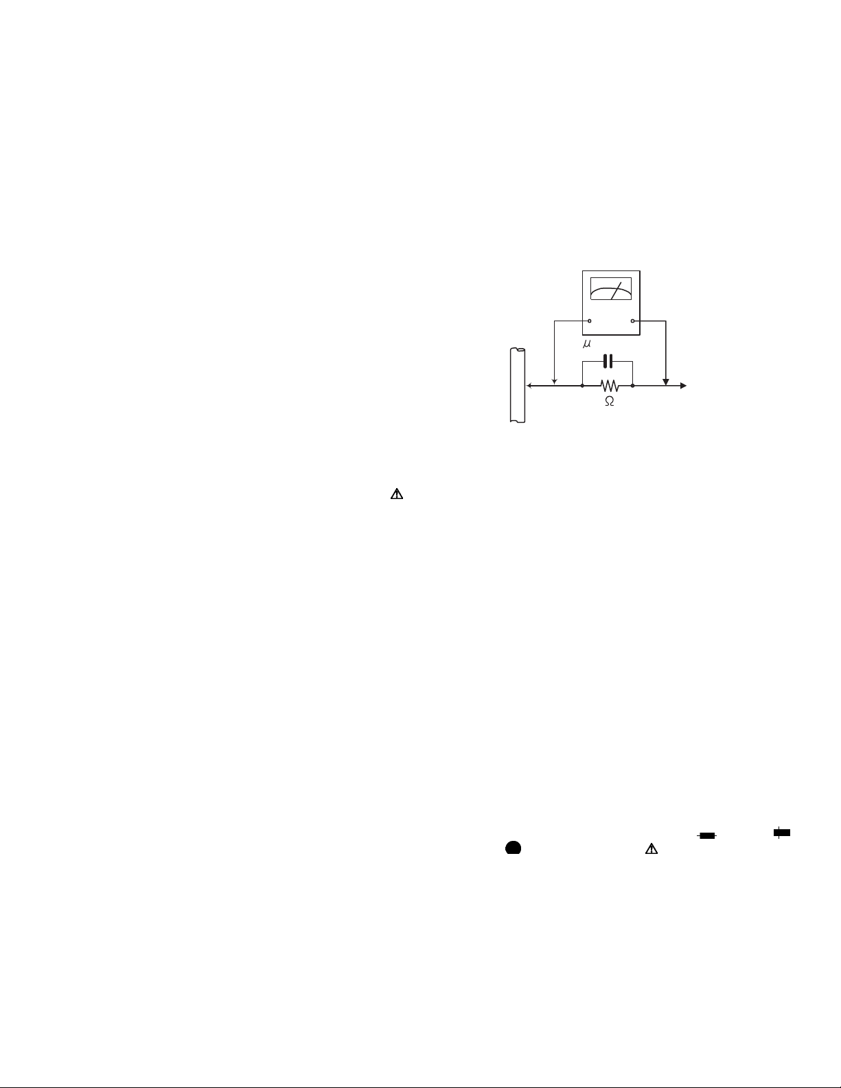
(5) Leakage shock hazard testing
After reassembling the product, always perform an isolation check on the exposed metal parts of the product (antenna terminals, knobs, metal cabinet, screw heads,
headphone jack, control shafts, etc.) to be sure the product
is safe to operate without danger of electrical shock.Do not
use a line isolation transformer during this check.
• Plug the AC line cord directly into the AC outlet. Using a
"Leakage Current Tester", measure the leakage current
from each exposed metal parts of the cabinet, particularly any exposed metal part having a return path to the
chassis, to a known good earth ground. Any leakage current must not exceed 0.5mA AC (r.m.s.).
• Alternate check method
Plug the AC line cord directly into the AC outlet. Use an
AC voltmeter having, 1,000Ω per volt or more sensitivity
in the following manner. Connect a 1,500Ω 10W resistor
paralleled by a 0.15µF AC-type capacitor between an ex-
posed metal part and a known good earth ground.
Measure the AC voltage across the resistor with the AC
voltmeter.
Move the resistor connection to each exposed metal
part, particularly any exposed metal part having a return
path to the chassis, and measure the AC voltage across
the resistor. Now, reverse the plug in the AC outlet and
repeat each measurement. Voltage measured any must
not exceed 0.75 V AC (r.m.s.). This corresponds to 0.5
mA AC (r.m.s.).
AC VOLTMETER
(Having 1000
ohms/volts,
or more sensitivity)
0.15 F AC TYPE
Place this
probe on
1500 10W
Good earth ground
1.2 Warning
(1) This equipment has been designed and manufactured to
meet international safety standards.
(2) It is the legal responsibility of the repairer to ensure that
these safety standards are maintained.
(3) Repairs must be made in accordance with the relevant
safety standards.
(4) It is essential that safety critical components are replaced
by approved parts.
(5) If mains voltage selector is provided, check setting for local
voltage.
1.3 Caution
Burrs formed during molding may be left over on some parts
of the chassis.
Therefore, pay attention to such burrs in the case of preforming repair of this system.
1.4 Critical parts for safety
In regard with component parts appearing on the silk-screen
printed side (parts side) of the PWB diagrams, the parts that are
printed over with black such as the resistor ( ), diode ( )
and ICP ( ) or identified by the " " mark nearby are critical
for safety. When replacing them, be sure to use the parts of the
same type and rating as specified by the manufacturer.
(This regulation dose not Except the J and C version)
each exposed
metal part.
(No.MB262)1-3
Page 4
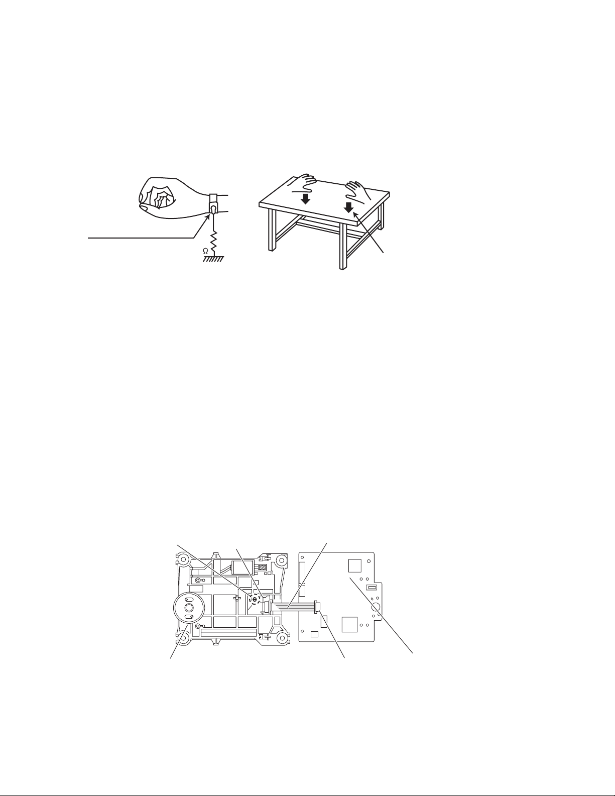
1.5 Preventing static electricity
Electrostatic discharge (ESD), which occurs when static electricity stored in the body, fabric, etc. is discharged, can destroy the laser
diode in the traverse unit (optical pickup). Take care to prevent this when performing repairs.
1.5.1 Grounding to prevent damage by static electricity
Static electricity in the work area can destroy the optical pickup (laser diode) in devices such as laser products.
Be careful to use proper grounding in the area where repairs are being performed.
(1) Ground the workbench
Ground the workbench by laying conductive material (such as a conductive sheet) or an iron plate over it before placing the
traverse unit (optical pickup) on it.
(2) Ground yourself
Use an anti-static wrist strap to release any static electricity built up in your body.
(caption)
Anti-static wrist strap
1M
Conductive material
(conductive sheet) or iron palate
(3) Handling the optical pickup
• In order to maintain quality during transport and before installation, both sides of the laser diode on the replacement optical
pickup are shorted. After replacement, return the shorted parts to their original condition.
(Refer to the text.)
• Do not use a tester to check the condition of the laser diode in the optical pickup. The tester's internal power source can easily
destroy the laser diode.
1.6 Handling the traverse unit (optical pickup)
(1) Do not subject the traverse unit (optical pickup) to strong shocks, as it is a sensitive, complex unit.
(2) Cut off the shorted part of the flexible cable using nippers, etc. after replacing the optical pickup. For specific details, refer to the
replacement procedure in the text. Remove the anti-static pin when replacing the traverse unit. Be careful not to take too long a
time when attaching it to the connector.
(3) Handle the flexible cable carefully as it may break when subjected to strong force.
(4) I t is not possible to adjust the semi-fixed resistor that adjusts the laser power. Do not turn it.
1.7 Attention when traverse unit is decomposed
*Please refer to "Disassembly method" in the text for the pickup unit.
• Apply solder to the short land sections before the flexible wire is disconnected from the connecto on the servo board. (If the flexible
wire is disconnected without applying solder, the pickup may be destroyed by static electricity.)
• In the assembly, be sure to remove solder from the short land sections after connecting the flexible wire.
Short land section
CD pickup
Card wire
1-4 (No.MB262)
Traverse mechanism assembly
CN601
CD servo board
Page 5
1.8 Important for laser products
!
1.CLASS 1 LASER PRODUCT
2.DANGER : Invisible laser radiation when open and inter
lock failed or defeated. Avoid direct exposure to beam.
3.CAUTION : There are no serviceable parts inside the
Laser Unit. Do not disassemble the Laser Unit. Replace
the complete Laser Unit if it malfunctions.
4.CAUTION : The CD,MD and DVD player uses invisible
laser radiation and is equipped with safety switches which
prevent emission of radiation when the drawer is open and
the safety interlocks have failed or are defeated. It is
dangerous to defeat the safety switches.
5.CAUTION : If safety switches malfunction, the laser is able
to function.
6.CAUTION : Use of controls, adjustments or performance of
procedures other than those specified here in may result in
hazardous radiation exposure.
Please use enough caution not to
see the beam directly or touch it
in case of an adjustment or operation
check.
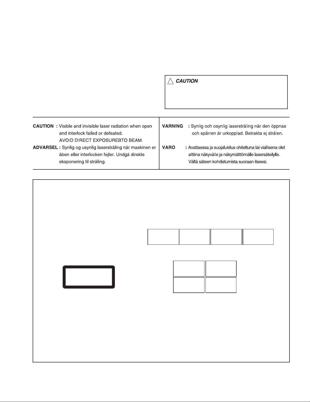
REPRODUCTION AND POSITION OF LABELS
WARNING LABEL
CAUTION : Visible and Invisible
laser radiation when open and
interlock failed or defeated.
AVOID DIRECT EXPOSURE TO
BEAM. (e)
CLASS 1
LASER PRODUCT
ADVARSEL : Synlig og usynlig
laserstråling når maskinen er
åben eller interlocken fejeler.
Undgå direkte eksponering til
stråling. (d)
CAUTION : Visible and Invisible
laser radiation when open and
interlock failed or defeated.
AVOID DIRECT EXPOSURE TO
BEAM. (e)
VARNING : Synlig och
osynling laserstrålning när
den öppnas och spärren är
urkopplad. Betrakta ej
strålen. (s)
VARNING : Synlig och
osynling laserstrålning när
den öppnas och spärren är
urkopplad. Betrakta ej
strålen. (s)
VARO : Avattaessa ja suojalukitus
ohitettuna tai viallisena olet alttiina
näkyvälle ja näkymättömälle
lasersäteilylle. Vältä säteen
kohdistumista suoraan itseesi. (f)
ADVARSEL : Synlig og usynlig
laserstråling når maskinen er
åben eller interlocken fejeler.
Undgå direkte eksponering til
stråling. (d)
VARO : Avattaessa ja suojalukitus
ohitettuna tai viallisena olet alttiina
näkyvälle ja näkymättömälle
lasersäteilylle. Vältä säteen
kohdistumista suoraan itseesi. (f)
(No.MB262)1-5
Page 6

SECTION 2
SPECIFIC SERVICE INSTRUCTIONS
This service manual does not describe SPECIFIC SERVICE INSTRUCTIONS.
1-6 (No.MB262)
Page 7
SECTION 3
DISASSEMBLY
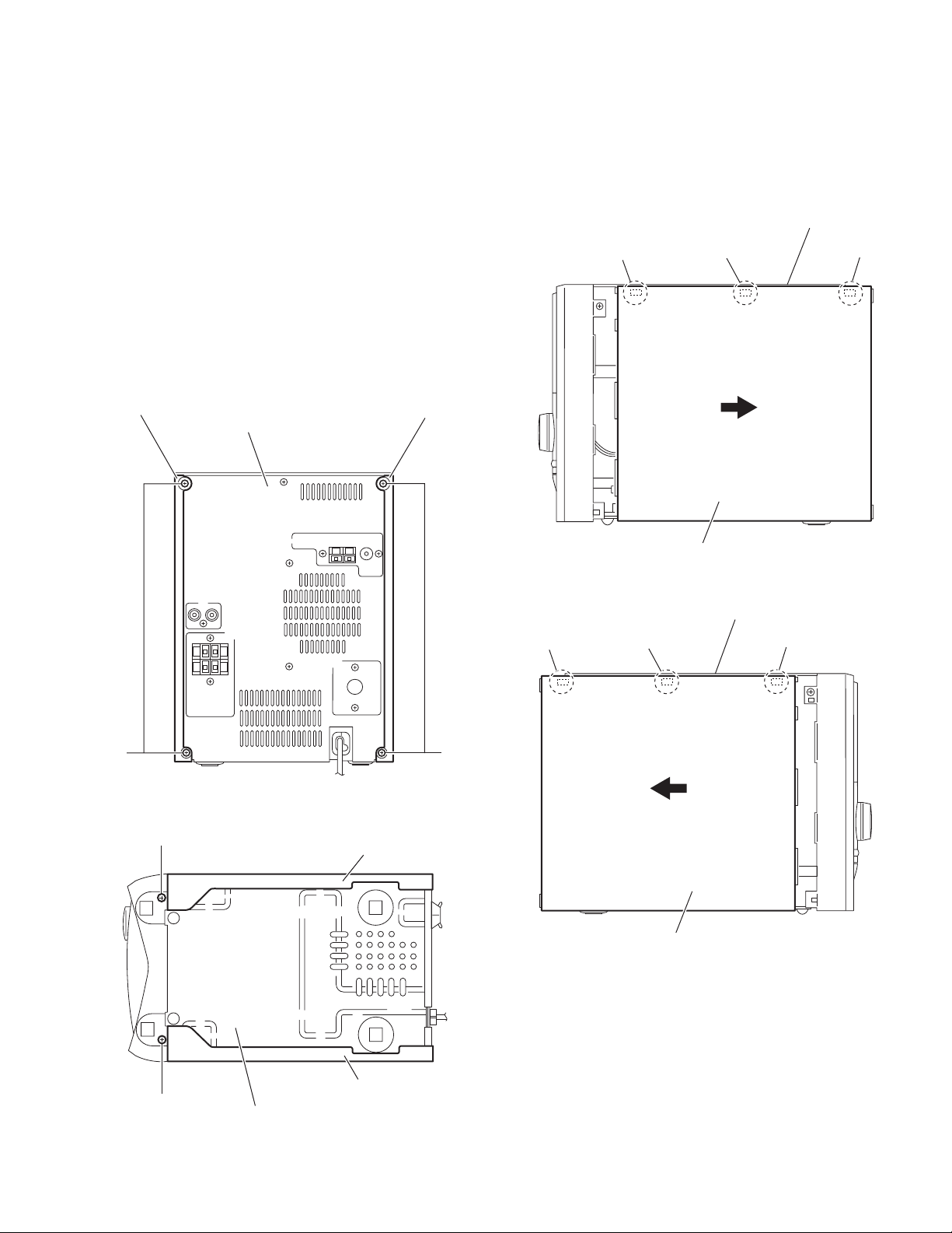
3.1 Main body section
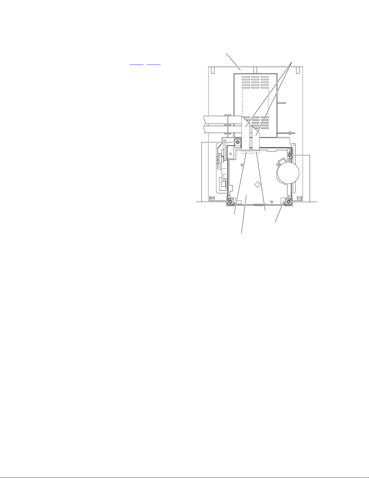
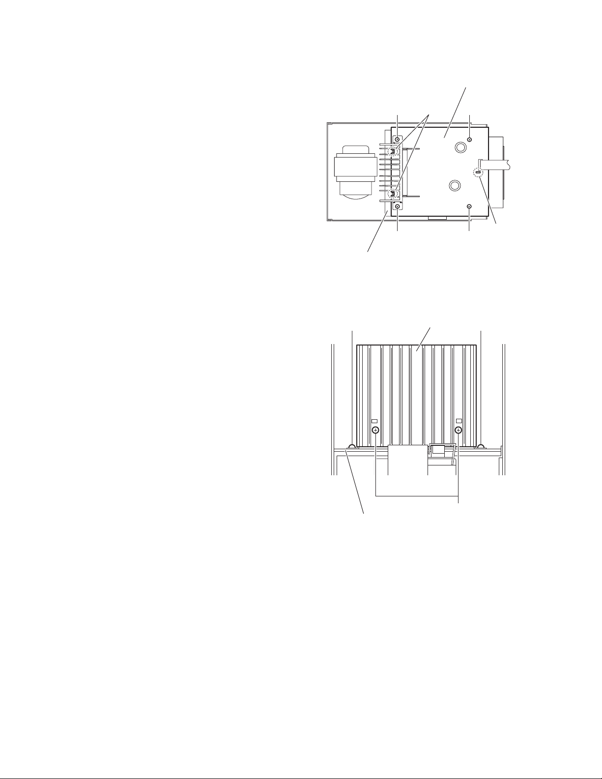
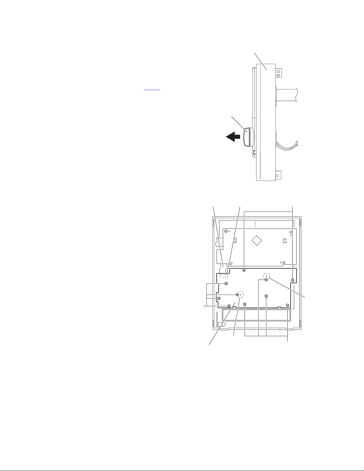
3.1.1 Removing the side panels L/R
(See Figs.1 to 4)
(1) From the back side of the main body, remove the four
screws A attaching the side panels L/R to the rear panel.
(See Fig.1.)
(2) From the bottom side of the main body, remove the two
screws B attaching the side panels L/R to the bottom chassis. (See Fig.2.)
(3) From the both sides of the main body, release the engage-
ment sections (a, b) of the side panels L/R from the top
cover assembly in the direction of the arrow. (See Figs.3
and 4.)
(4) Remove the side panels L/R toward this side.
Top cover assembly
a
a
a
Side panel R
A
B
Rear panel
Fig.1
Side panel L
Side panel R
A
Side panel R
Fig.3
Top cover assembly
b
b
b
B
Side panel L
Fig.4
Side panel L
Bottom chassis
Fig.2
(No.MB262)1-7
Page 8
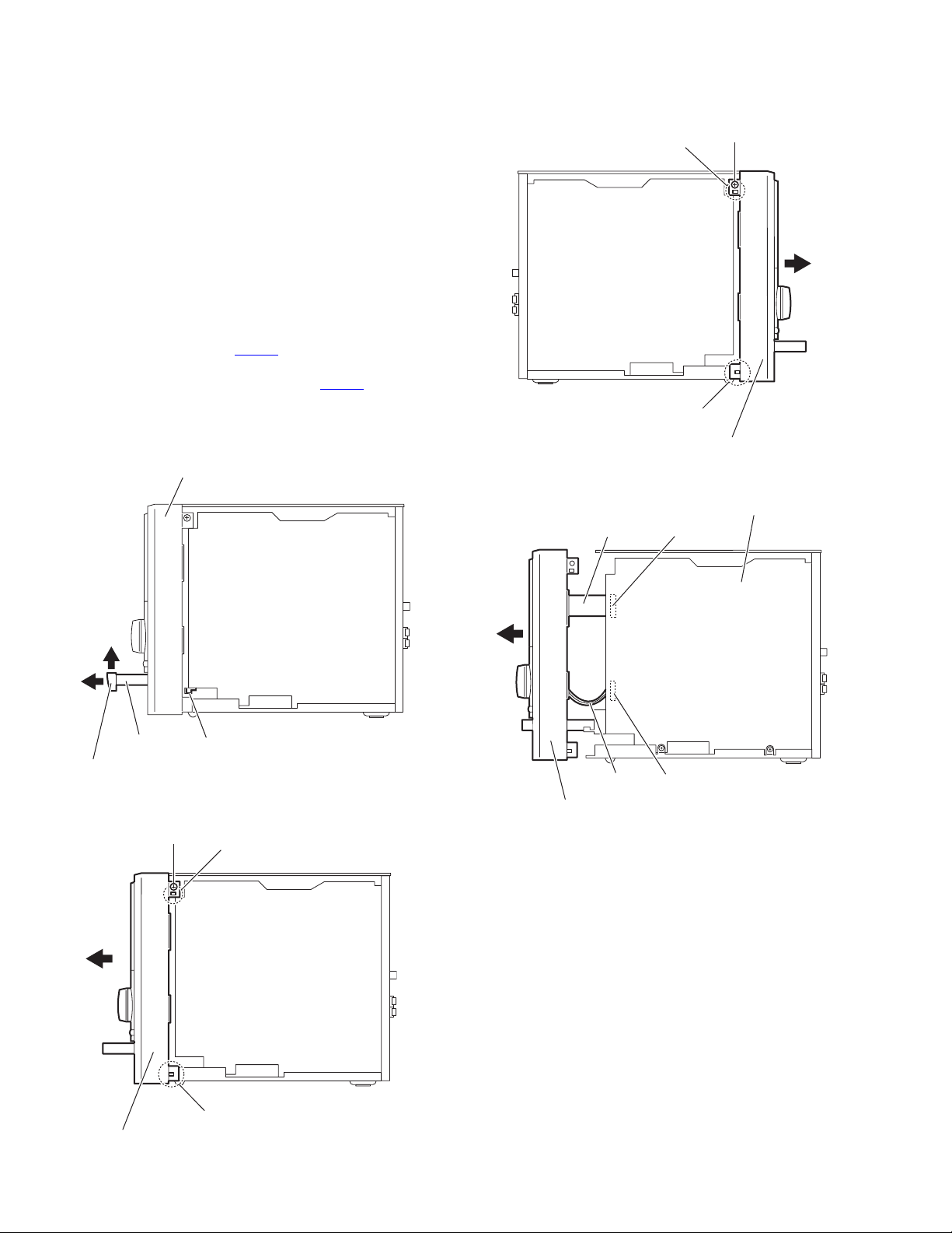
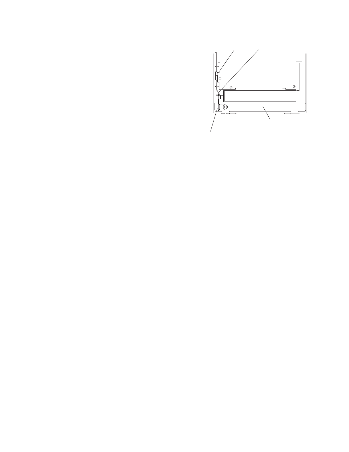
3.1.2 Removing the front panel assembly
(See Figs.5 to 8)
• Prior to performing the following procedures, remove the side
panels L/R.
(1) From the right side of the main body, push the slide cam
and pull the tray out of the main body in the direction of the
arrow 1. (See Fig.5.)
(2) Remove the tray fitting from the tray in the direction of the
arrow 2. (See Fig.5.)
(3) From the both sides of the main body, remove the two
screws C attaching the front panel assembly. (See Figs.6
and 7.)
(4) Release the two claws c and claws d to draw out the front
panel assembly in the direction of the arrow. (See Figs.6
and 7.)
(5) From the right side of the main body, disconnect the card
wire from the connector CN730
Fig.8.)
(6) Disconnect the wire from the connector CN271
board. (See Fig.8.)
(7) Remove the front panel assembly in the direction of the ar-
row. (See Fig.8.)
Front panel assembly
on the main board. (See
on the main
c
Front panel assembly
Fig.7
CN730Card wire
C
d
Main board
2
1
Tray fitting
Tray
Slide cam
C
Fig.5
c
Wire
Front panel assembly
CN271
Fig.8
Front panel assembly
1-8 (No.MB262)
d
Fig.6
Page 9
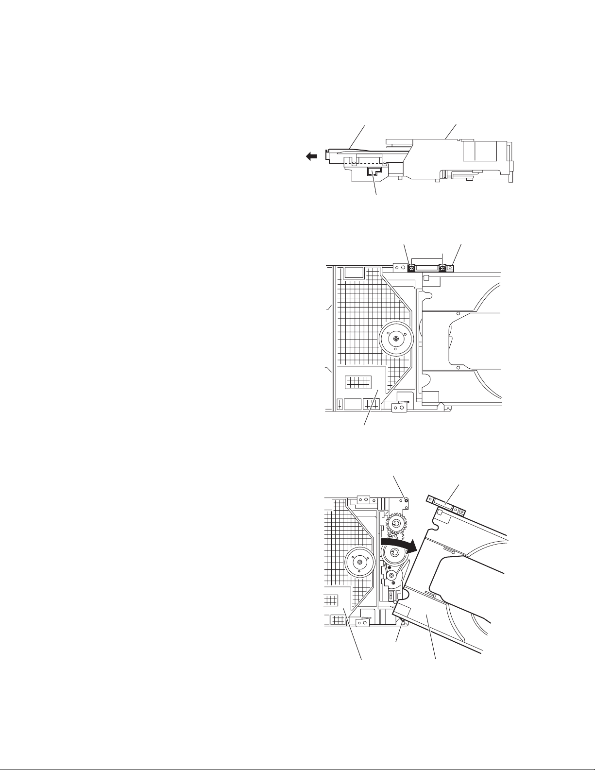
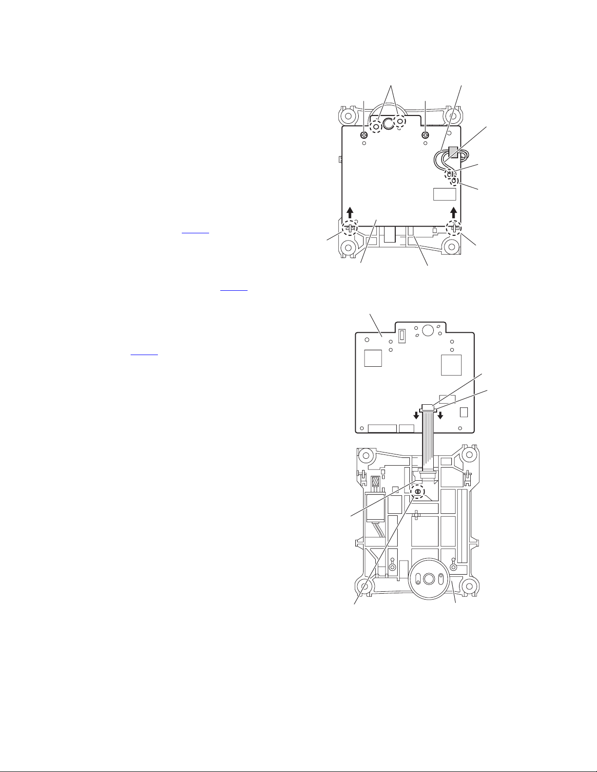
3.1.3 Removing the top cover assembly
(See Figs.9 and 10)
• Prior to performing the following procedures, remove the side
panels L/R and front panel assembly.
(1) From the back side of the main body, remove the screw D
attaching the top cover assembly to the rear panel. (See
Fig.9.)
(2) From the right side of the main body, disconnect the card
wires from the connectors (CN701
board. (See Fig.10.)
(3) Take out the top cover assembly from the main body.
, CN702) on the main
Top cover assembly
D
Rear panel
Fig.9
Top cover assembly
CN702
Main board
Fig.10
Card wires
CN701
(No.MB262)1-9
Page 10
3.1.4 Removing the cassette mechanism assembly
(See Fig.11)
• Prior to performing the following procedures, remove the side
panels L/R, front panel assembly and top cover assembly.
(1) From the bottom side of the top cover assembly, discon-
nect the card wires from the connectors (CN33
the head amp. & mechanism control board.
(2) Remove the four screws E attaching the cassette mecha-
nism assembly and take out the cassette mechanism assembly from the top cover assembly.
, CN34) on
Top cover assembly
Card wires
E
CN34
Head amp. & mechanism control board
CN33
Cassette mechanism assembly
Fig.11
E
1-10 (No.MB262)
Page 11
3.1.5 Removing the tuner
(See Figs.12 and 13)
• Prior to performing the following procedures, remove the side
panel L.
(1) From the back side of the main body, remove the two
screws F attaching the tuner to the rear panel. (See
Fig.12.)
(2) Disconnect the card wire from the connector CN1
tuner. (See Fig.13.)
on the
F
Rear panel
Card wire
Tuner
Fig.12
CN1
Fig.13
(No.MB262)1-11
Page 12
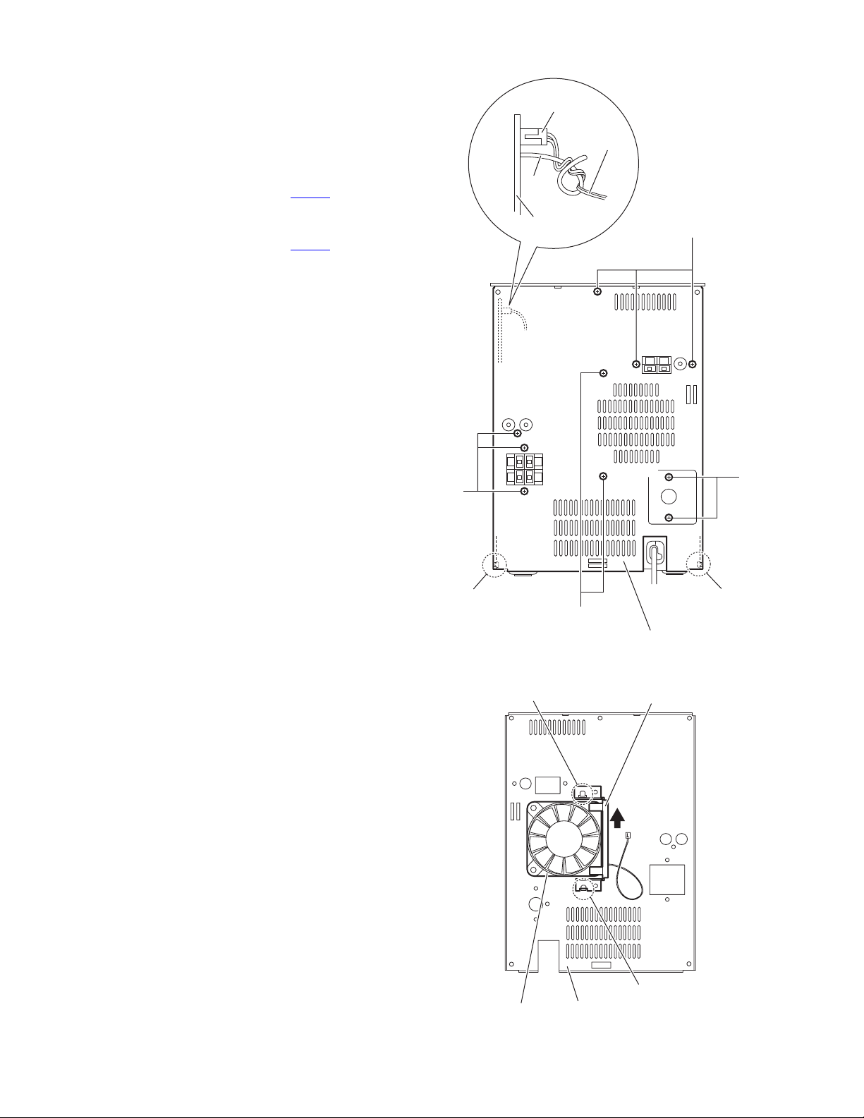
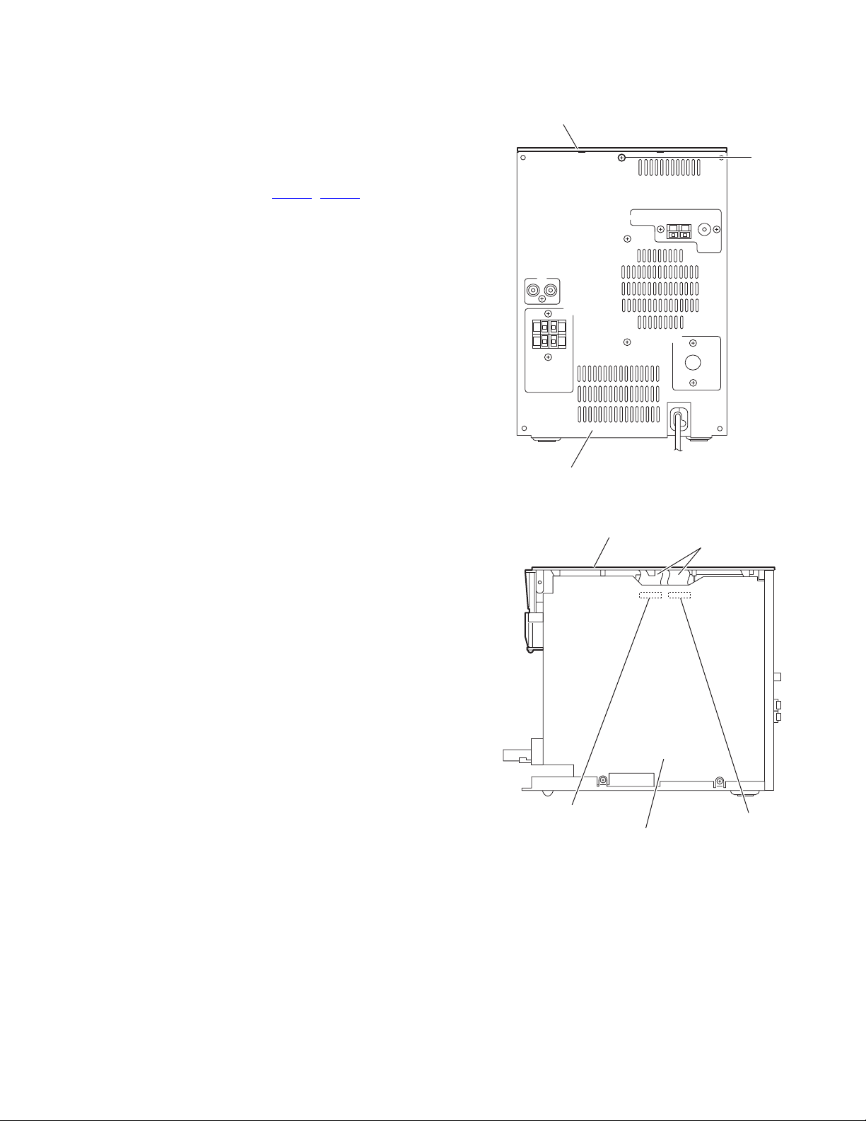
3.1.6 Removing the rear panel
(See Fig.14)
• Prior to performing the following procedures, remove the side
panels L/R.
(1) From the back side of the main body, remove the eight
screws G attaching the rear panel.
(2) Release the engagement sections e and remove the rear
panel.
(3) Disconnect the wire from the connector CN711
board.
Reference:
After connecting the wire to the connector CN711
with the wire holder.
3.1.7 Removing the fan
(See Figs.14 and 15)
• Prior to performing the following procedures, remove the side
panels L/R and rear panel.
(1) From the outside of the rear panel, remove the two screws
H attaching the fan bracket to the rear panel. (See Fig.14.)
(2) From the inside of the rear panel, move the fan bracket in
the direction of the arrow to release the engagement sections (f, g). (See Fig.15.)
(3) Remove the fan bracket from the rear panel and remove
the fan. (See Fig.15.)
on the main
, fix the wire
CN711
Wire
holder
Main board
Wire
G
G
G
e
e
H
Rear panel
Fig.14
f
Fan bracket
1-12 (No.MB262)
Fan
g
Rear panel
Fig.15
Page 13
3.1.8 Removing the main board
(See Fig.16)
• Prior to performing the following procedures, remove the side
panels L/R, front panel assembly, top cover assembly, tuner
and rear panel.
(1) From the right side of the main body, remove the two
screws J attaching the main board.
(2) Remove the main board toward this side and disconnect
the connector CN200
(3) From the forward side of the main board, disconnect the
card wires from the connectors (CN210
on the main board.
, CN221).
CN210
Main board
3.1.9 Removing the power supply board
(See Fig.17)
• Prior to performing the following procedures, remove the side
panel L and rear panel.
(1) From the left side of the main body, remove the screw K at-
taching the power supply board.
(2) Remove the power supply board toward this side and dis-
connect the connector CN104
(3) From the forward side of the power supply board, discon-
nect the wires from the connectors (CN101
CN103, CN105).
Reference:
When attaching the power supply board, insert the section h of
the power supply board in the hole of the bottom chassis before attaching the screw K.
on the power supply board.
, CN102,
CN102
CN101
h
CN200
CN103
CN105
J
Card wire
Fig.16
K
J
CN221
Power supply board
CN104
Fig.17
(No.MB262)1-13
Page 14
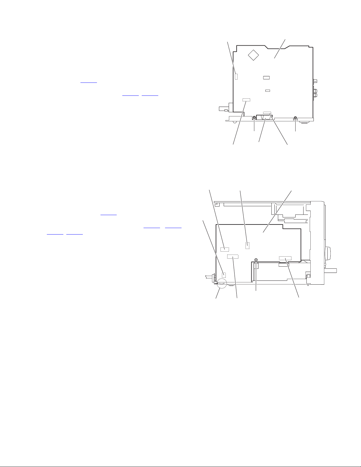
3.1.10 Removing the power amplifier board
(See Fig.18)
• Prior to performing the following procedures, remove the side
panels L/R, front panel assembly, top cover assembly, tuner,
rear panel, main board and power supply board.
(1) From the top side of the main body, remove the four screws
L attaching the power amplifier board.
(2) Lift the power amplifier board and remove it from the en-
gagement sections (i, j) of the shield case.
3.1.11 Removing the heat sink
(See Fig.19.)
• Prior to performing the following procedure, remove the side
panels L/R, front panel assembly, top cover assembly, tuner,
rear panel, main board, power supply board and power amplifier board.
(1) From the side of the power amplifier board, remove the two
screws M attaching the heat sink.
(2) From the side of the power amplifier board, remove the two
screws N attaching the heat sink.
Power amplifier board
L
i
L
LL
Shield case
Fig.18
M M
Heat sink
j
1-14 (No.MB262)
Power amplifier board
Fig.19
N
Page 15
3.1.12 Removing the CD mechanism assembly
(See Figs.20 and 21)
• Prior to performing the following procedures, remove the side
panels L/R, front panel assembly, top cover assembly, tuner,
rear panel, main board and power supply board.
(1) From the top side of the main body, remove the four screws
P attaching the shield case to the bottom chassis. (See
Fig.20.)
Reference:
When attaching the shield case on the bottom chassis,
align the projections (k, m, n) of the bottom chassis in the
holes of the shield case. (See Fig.20.)
(2) Take out the shield case with the power amplifier board
from the bottom chassis.
(3) Remove the three screws Q attaching the CD mechanism
assembly to the bottom chassis. (See Fig.21.)
P
Shield case
k
Bottom chassis
P
m
Power amplifier board
CD mechanism assembly
Bottom chassis
n
P
Fig.20
Q
Q
Fig.21
(No.MB262)1-15
Page 16
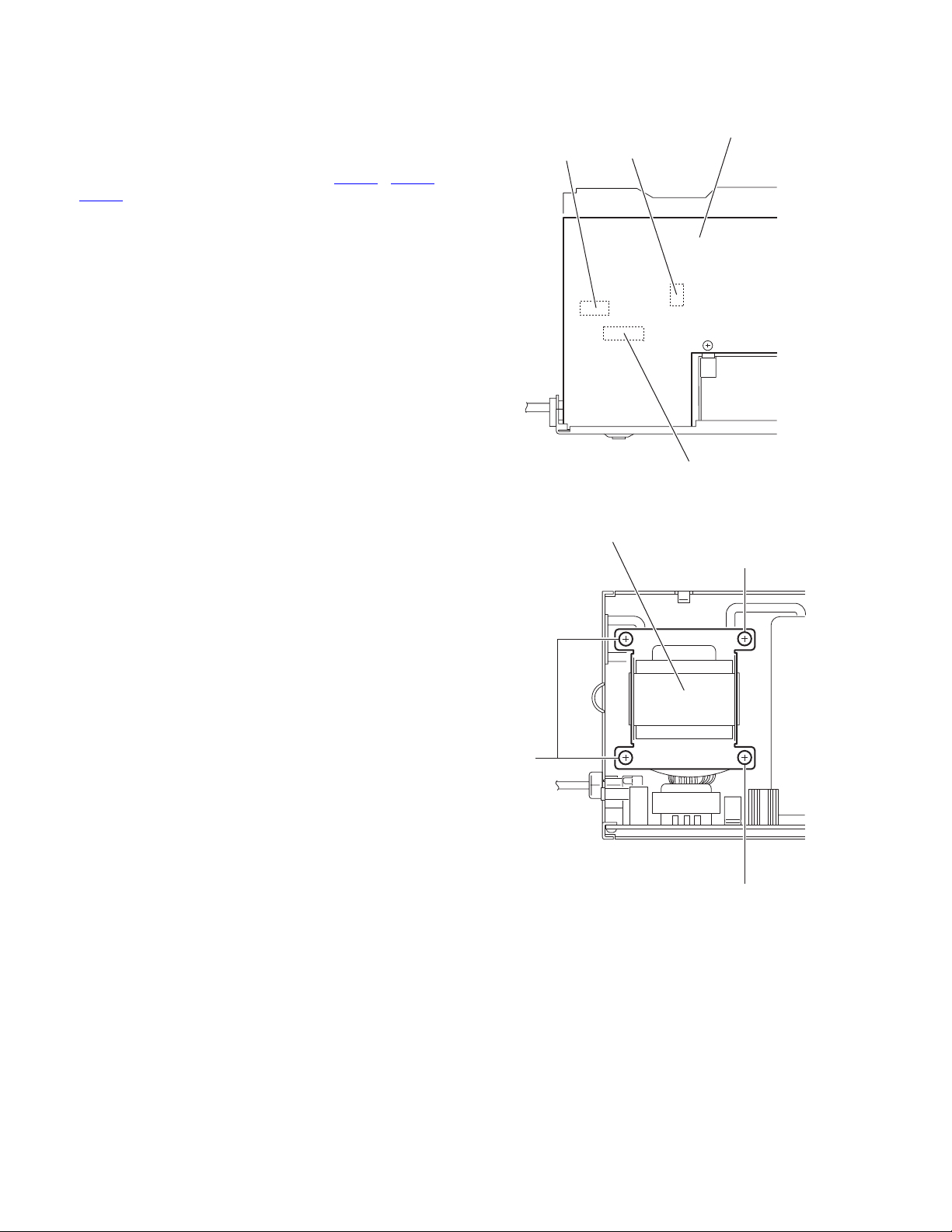
3.1.13 Removing the power transformer
(See Figs.22 and 23)
• Prior to performing the following procedures, remove the side
panels L/R, front panel assembly, top cover assembly and rear
panel.
(1) From the forward side of the power supply board, discon-
nect the wires from the connectors (CN102
CN105). (See Fig.22.)
Reference:
Remove the power supply board as required. (See
Fig.17.)
(2) From the top side of the main body, remove the four screws
R attaching the power transformer. (See Fig.23.)
, CN103,
CN102
Power supply board
CN103
CN105
Fig.22
Power transformer
R
R
R
Fig.23
1-16 (No.MB262)
Page 17
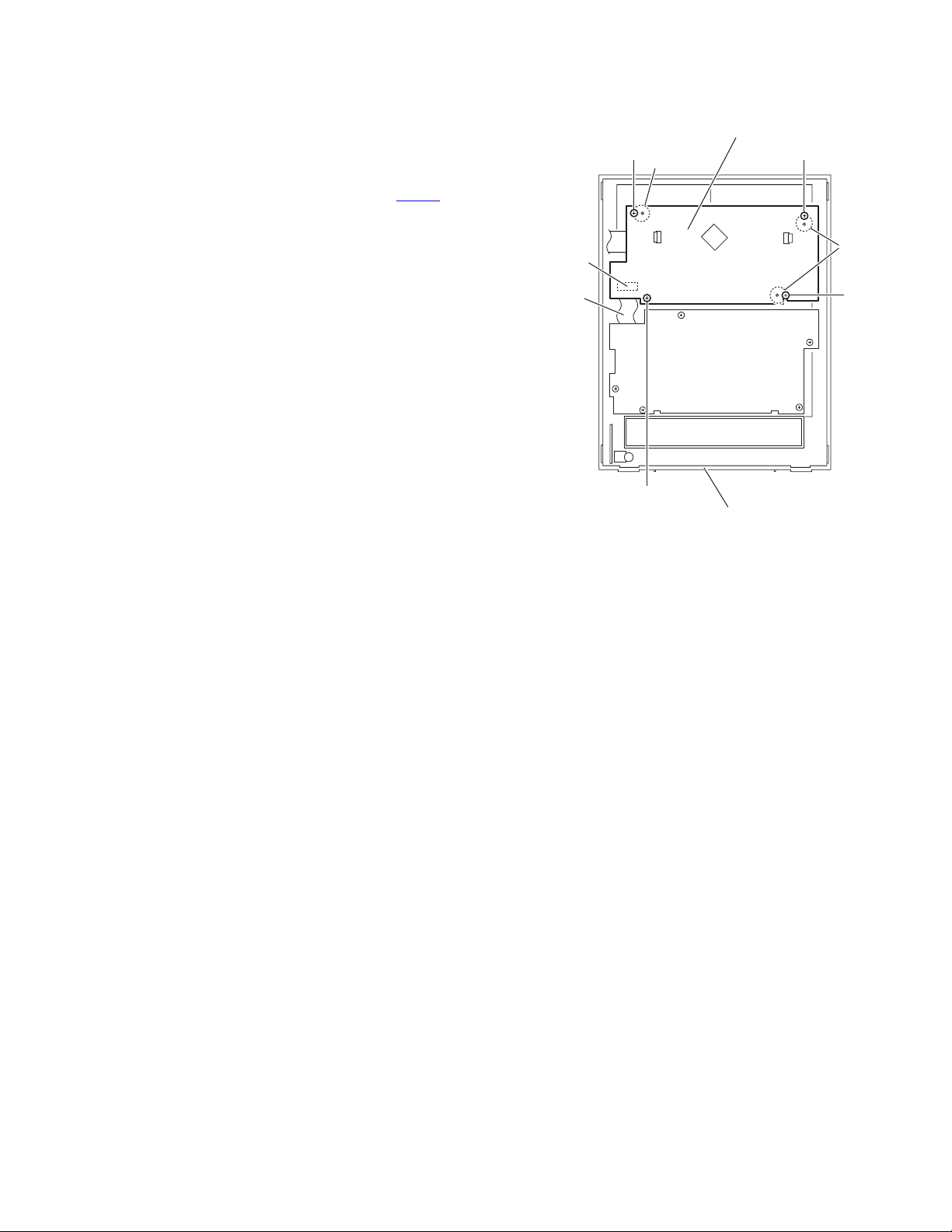
3.1.14 Removing the FL board
(See Fig.24)
• Prior to performing the following procedures, remove the side
panels L/R and front panel assembly.
(1) From the inside of the front panel assembly, remove the
four screws S attaching the FL board.
(2) Take out the FL board from the front panel assembly and
disconnect the card wire from the connector CN751
FL board.
Reference:
When attaching the FL board, align the projections p of the
front panel assembly in the holes of the FL board.
on the
CN751
Card
wire
S
FL board
p
S
p
S
S
Front panel assembly
Fig.24
(No.MB262)1-17
Page 18
3.1.15 Removing the switch board
(See Figs.25 and 26)
• Prior to performing the following procedures, remove the side
panels L/R and front panel assembly.
(1) From the front side of the front panel assembly, pull out the
mic volume knob. (See Fig.25.)
(2) From the inside of the front panel assembly, remove the
ten screws T attaching the switch board. (See Fig.26.)
(3) Take out the switch board from the front panel assembly
and disconnect the card wire from the connector CN760
the switch board. (See Fig.26.)
Reference:
When attaching the switch board, align the projections q of the
front panel assembly in the holes of the switch board. (See
Fig.26.)
on
Front panel assembly
Mic volume knob
Fig.25
Card wire
T
Switch board
CN760
q
T
q
T
Fig.26
1-18 (No.MB262)
Page 19
3.1.16 Removing the headphone jack board
(See Fig.27)
• Prior to performing the following procedure, remove the side
panels L/R and front panel assembly.
(1) From the inside of the front panel assembly, remove the
screw U attaching the headphone jack board.
Reference:
After attaching the headphone jack board, fix the wire with the
spacer.
Spacer
Wire
U
Headphone jack board
Fig.27
Front panel assembly
(No.MB262)1-19
Page 20
3.2 CD mechanism section
• Remove the CD mechanism assembly from the main body.
(See "3.1.12 Removing the CD mechanism assembly".)
3.2.1 Removing the tray assembly
(See Figs.1 to 3)
(1) From the right side of the CD mechanism assembly, push
the slide cam and pull the tray assembly out of the CD
mechanism assembly in the direction of the arrow. (See
Fig.1)
(2) From the top side of the CD mechanism assembly, remove
the two screws A attaching the leaf spring to the bushing
and remove the leaf spring. (See Fig.2)
(3) Remove the bushing of the tray assembly from the projec-
tion a on the CD mechanism assembly and move the tray
assembly in the direction of the arrow. (See Fig.3)
(4) Remove the claw b of the tray assembly from the CD
mechanism assembly and take out the tray assembly. (See
Fig.3)
Tray assembly CD mechanism assembly
Slide cam
Fig.1
Leaf spring
Bushing
A
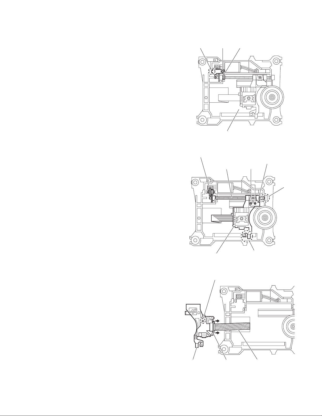
3.2.2 Removing the traverse mechanism assembly
(See Figs.4)
(1) From the bottom side of the CD mechanism assembly, re-
move the four screws B attaching the traverse mechanism
1-20 (No.MB262)
CD mechanism assembly
Projection a
Claw b
CD mechanism assembly
assembly.
Fig.2
Bushing
Tray assembly
Fig.3
Page 21
(2) Disconnect the card wire from the connector CN602
CD servo board and take out the CD traverse mechanism
assembly with the CD servo board.
on the
CD mechanism assembly
CD servo board
B
Traverse mechanism assembly
Fig.4
B
CN602
(No.MB262)1-21
Page 22
3.2.3 Removing the CD servo board
(See Figs.5 and 6)
• Remove the traverse mechanism assembly.
(1) From the bottom side of the traverse mechanism assem-
bly, remove the solders from the solder sections c. (See
Fig.5)
(2) Remove the wire (yellow) from the solder sections d. (See
Fig.5)
(3) Remove the wire (white) from the solder sections e. (See
Fig.5)
(4) Remove the two screws C attaching the CD servo board.
(See Fig.5)
(5) Remove the CD servo board from the claws f in the direc-
tion of the arrow and turn the CD servo board over. (See
Fig.5)
(6) Solder the short land sections g on the CD pickup. (See
Fig.6)
(7) Release the lock of the connector CN601
board in the direction of the arrow and disconnect the card
wire. (See Fig.6)
Caution:
• Solder the short land sections g on the CD pickup before disconnecting the card wire from the connector CN601
CD servo board. If the card wire is disconnected without attaching solder, the CD pickup may be destroyed by static
electricity. (See Fig.6)
• When attaching the CD servo board, be sure to remove solders from the short land sections g after connecting the card
wire to the connector CN601
Fig.6)
on the CD servo board. (See
on the CD servo
on the
Claw f
Solder section c
CD servo board
Wire (yellow)
CC
Wire (white)
Solder
section d
Solder
section e
Claw f
Traverse mechanism assemblyCD servo board
Fig.5
CN601
CD pickup
Short land section g
Lock
Traverse mechanism assembly
Fig.6
1-22 (No.MB262)
Page 23
3.2.4 Removing the CD pickup
(See Figs.7 to 9)
• Remove the traverse mechanism assembly.
(1) From the top side of the traverse mechanism assembly, re-
move the screw D attaching the shaft holder. (See Fig.7)
(2) Release the joint h and take out the shaft holder. (See
Fig.7)
(3) Remove the two screws E attaching the rack arm and take
out the rack arm. (See Fig.8)
(4) Remove the feed middle gear and remove the screw shaft
of the CD pickup from the section i on the traverse mechanism assembly. (See Fig.8)
(5) Remove the CD pickup from the section j of the traverse
mechanism assembly and take out the CD pickup with the
screw shaft. (See fig.8)
(6) Pull the screw shaft out of the CD pickup. (See Fig.8)
(7) From the bottom side of the CD pickup, solder the short
land sections k on the CD pickup. (See Fig.9)
(8) Release the lock of the connector on the CD pickup in the
direction of the arrow and disconnect the card wire. (See
Fig.9)
Caution:
• Solder the short land sections k on the CD pickup before dis-
connecting the card wire from the connector on the CD pickup. If the card wire is disconnected without attaching solder,
the CD pickup may be destroyed by static electricity. (See
Fig.9)
• When attaching the CD pickup, be sure to remove solders
from the short land sections k after connecting the card wire
to the connector on the CD pickup. (See Fig.9)
Traverse mechanism assembly
Feed middle gear
Screw shaft
DJoint h
Shaft holder
Fig.7
Rack arm
E
Section i
CD pickup
Short land section k
CD pickup Connector Card wire
Section j
Fig.8
Fig.9
(No.MB262)1-23
Page 24
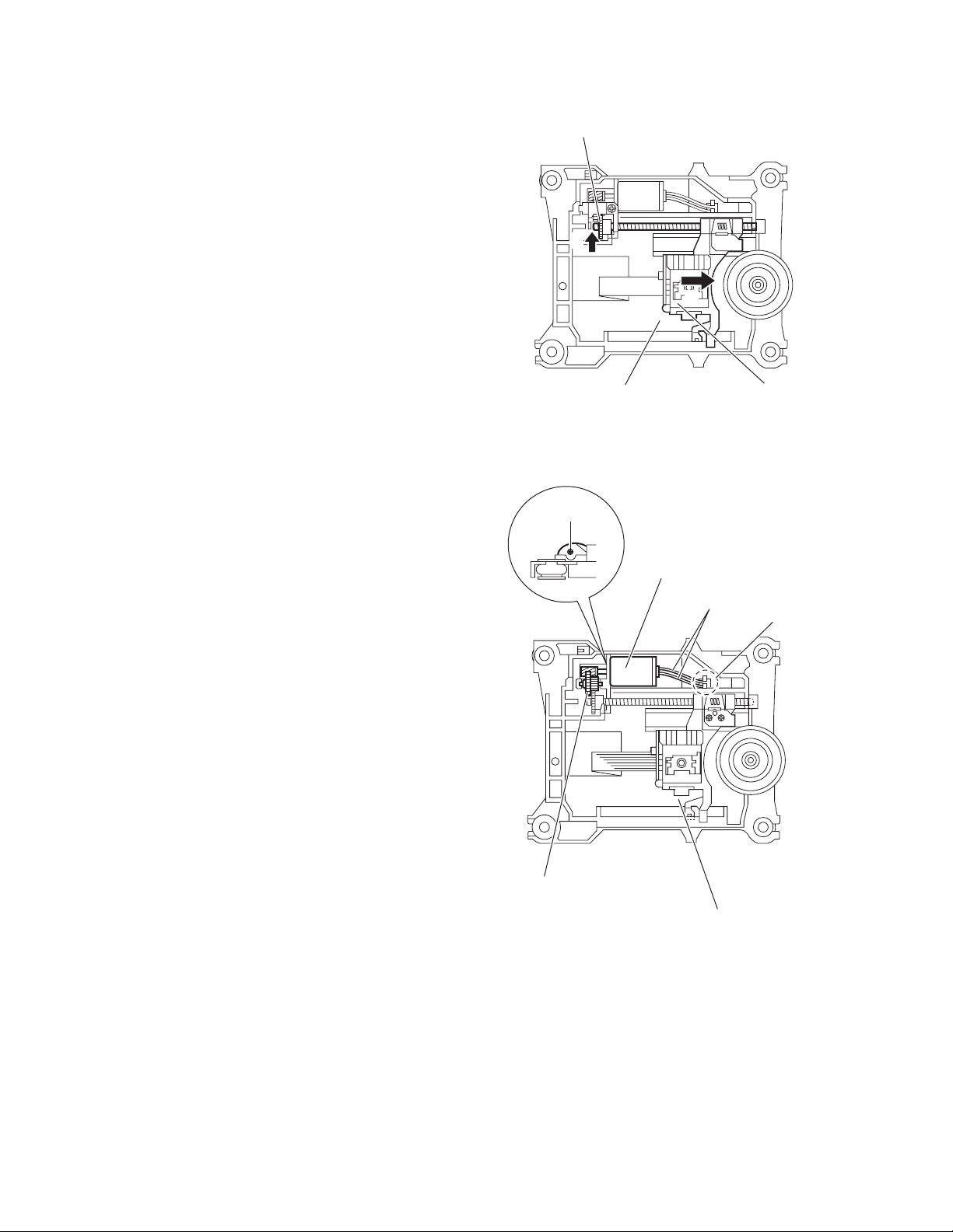
3.2.5 Attaching the CD pickup
(See Figs.7 to 10)
• See "3.2.4 Removing the CD pickup".
(1) Remove solders from the short land sections k after con-
necting the card wire to the connector on the CD pickup.
(See Fig.9)
(2) Attach the shaft. (See Fig.8)
(3) Align the CD pickup to the section j of the traverse mecha-
nism assembly first, and set the screw shaft of the CD pick-
up in the sections i of the traverse mechanism assembly.
(See Fig.8.)
(4) Attach the rack arm and feed middle gear. (See Fig.8)
(5) Attach the shaft holder. (See Fig.7)
(6) Turn the SS gear in the direction of the arrow 1 to move the
CD pickup in the direction of the arrow 2. (See Fig.10)
SS gear
1
2
3.2.6 Removing the feed motor
(See Figs.5, 7 and 11)
• Remove the traverse mechanism assembly.
(1) From the top side of the traverse mechanism assembly, re-
move the wire (yellow) from the solder sections d on the
CD servo board. (See Fig.5)
(2) Remove the wire (white) from the solder sections e on the
CD servo board. (See Fig.5)
(3) Remove the screw D attaching the shaft holder and take
out the shaft holder. (See Fig.7)
(4) Remove the feed middle gear and remove the screw E at-
taching the feed motor. (See Fig.11)
(5) Take out the feed motor from the traverse mechanism as-
sembly.
Reference:
When attaching the feed motor, pass the wires through the
section m on the traverse mechanism assembly. (See Fig.11)
Traverse mechanism assembly
Fig.10
E
Feed motor
Wires
Pickup
Section m
1-24 (No.MB262)
Feed middle gear
Traverse mechanism assembly
Fig.11
Page 25
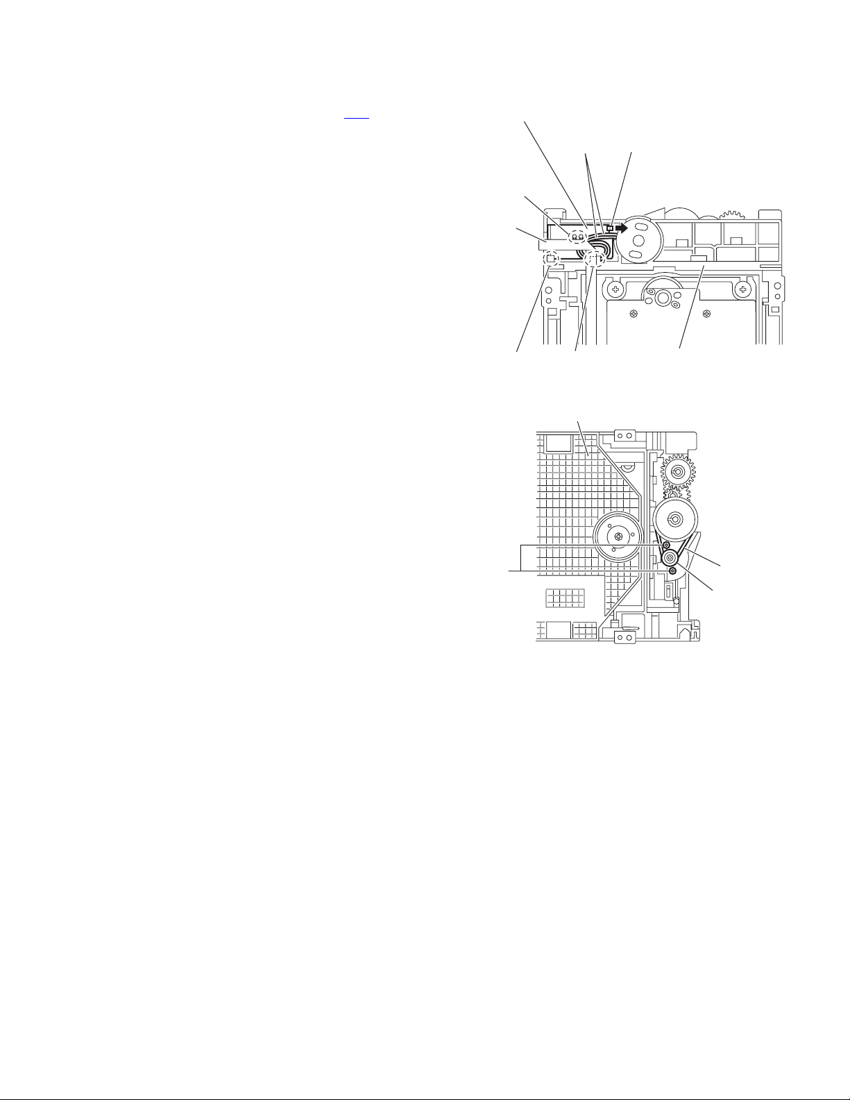
3.2.7 Removing the CD loading switch board
(See Fig.12)
(1) From the bottom side of the CD mechanism assembly, dis-
connect the card wire from the connector CN1
loading switch board.
(2) Remove the wires from the solder section n on the CD
loading switch board.
(3) Lift the CD loading switch board while pressing the claw p
of the CD mechanism assembly in the direction of the arrow and remove it from the section q.
Reference:
• Put the wires on the section r after attaching the CD loading
switch board to the CD mechanism assembly.
• Fix the claw p on the CD mechanism assembly with bonds
after attaching the CD loading switch board.
3.2.8 Removing the motor
(See Figs.12 and 13)
• Remove the tray assembly.
(1) From the bottom side of the CD mechanism assembly, re-
move the wires from the solder section n on the CD loading
switch board. (See Fig.12)
(2) From the top side of the CD mechanism assembly, remove
the belt from the motor pulley. (See Fig.13)
Note:
Take care not to attach grease on the belt.
(3) Remove the two screws F attaching the motor to the CD
mechanism assembly and take out the motor from the bottom side of the CD mechanism assembly. (See Fig.13)
Reference:
Put the wires on the section r after attaching the motor to the
CD mechanism assembly. (See Fig.12)
on the CD
CD loading switch board
Wire
Solder
section n
CN1
section q section r
CD mechanism assembly
F
Claw p
CD mechanism assembly
Fig.12
Belt
Fig.13
Motor pulley
(No.MB262)1-25
Page 26
3.3 Cassette mechanism assembly
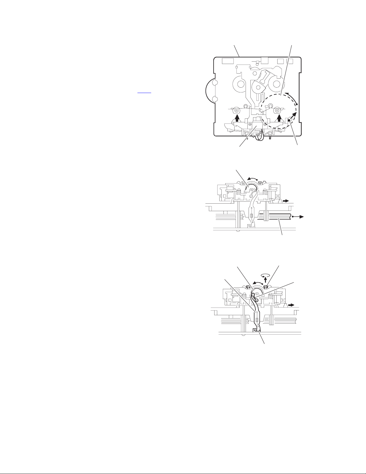
3.3.1 Removing the Play/Record & Clear head
(See Fig.1~3)
(1) While moving the trigger arm on the right side of the head
mount in the direction of the arrow, turn the flywheel R
counterclockwise until the head mount comes ahead and
clicks.
(2) The head turns counterclockwise as you turn the flywheel
R counterclockwise (See Fig.2 and 3).
(3) Disconnect the flexible wire from connector CN31
head amplifier & mechanism control board.
(4) Remove the spring from the back of the head.
(5) Loosen the azimuth screw for reversing attaching the head.
(6) Remove the head on the front side of the head mount.
on the
Cassette mechanism assembly
Fig.1
Head
Fly wheelR
Trigger armHead mount
Flexible wire
Fly wheel R
Fig.2
Azimuth screw
Head
for reversing
Spring
CN31
Head amplifer & mecha control board
Fig.3
1-26 (No.MB262)
Page 27
3.3.2 Removing the head amplifier & mechanism control board
(See Fig.4)
(1) Turn over the cassette mechanism assembly and remove
the three screws A attaching the head amplifier & mechanism control board.
(2) Disconnect the flexible wire from connector CN31
head amplifier & mechanism control board.
(3) Disconnect connector CN32
anism control board from connector CN1
board.REFERENCE: If necessary, unsolder the 4-pin wire
soldered to the main motor.
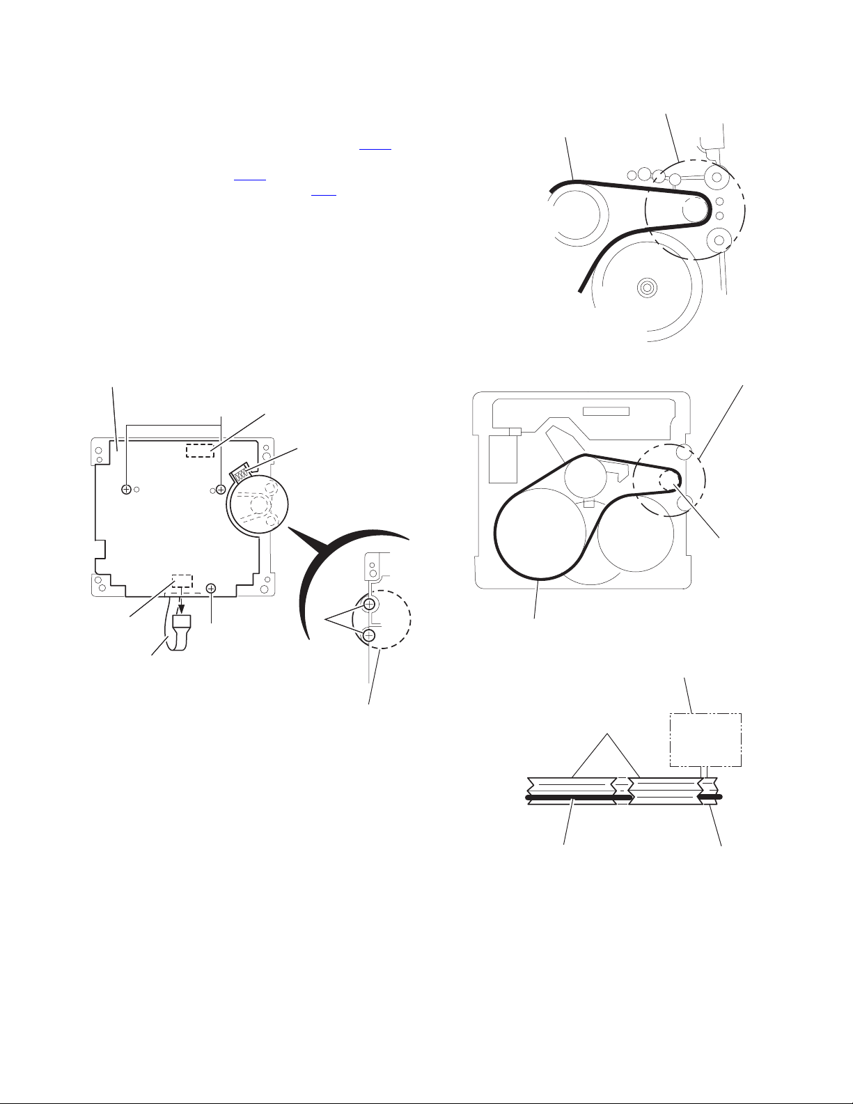
3.3.3 Removing the main motor
(See Fig.4~7)
(1) Remove the two screws B .
(2) Half raise the motor and remove the capstan belt from the
motor pulley.
ATTENTION:
Be careful to keep the capstan belt from grease. When reassembling, refer to Fig.6 and 7 for attaching the capstan belt.
Head amplifier & mecha control board
of the head amplifier & mech-
on the reel pulse
on the
Main motor assembly
Capstan belt
Fig.5
Main motor assembly
CN31
Flexible wire
A
AA
Fig.4
CN32
4pin wire
B
Main motor assembly
Motor pulley
Capstan belt
Fig.6
Main motor assembly
Fly wheel
Capstan belt
Motor pulley
Fig.7
(No.MB262)1-27
Page 28

3.3.4 Removing the flywheel
(See Fig.8, 9)
• Prior to performing the following procedure, remove the head
amplifier & mechanism control board and the main motor assembly.
(1) From the front side of the cassette mechanism, remove the
slit washers attaching the capstan shaft L and R. Pull out
the flywheels backward.
Fly wheel R Fly wheel L
Fig.8
Fly wheel R
Capstan shaft R Capstan shaft L
Slit washer
Fig.9
3.3.5 Removing the reel pulse board and solenoid
(See Fig.10)
• Prior to performing the following procedure, remove the head amplifier & mechanism control board.
(1) Remove the screw C.
(2) Release the tab a, b, c, d and e retaining the reel pulse board.
(3) Release the tab f and g attaching the solenoid on the reel pulse board.
(4) The reel pulse board and the solenoid come off.
Fly wheel L
bc
a
Solenoid
g
f
d
Reel pulse board
C
e
Fig.10
1-28 (No.MB262)
Page 29

3.3.6 Reattaching the Play/ Record & Clear head
r
r
(See Fig.11~13)
(1) Reattaching the head mount assembly.
a) Change front of the direction cover of the head
mount assembly to the left (Turn the head forward).
b) Fit the bosses O', P', Q', U' and V' on the head mount
assembly to the holes P and V, the slots O, U and Q
of the mechanism sub assembly (See Fig.11 to 13).
CAUTION:
To remove the head mount assembly, turn the direction
cover to the left to disengage the gear. If the gear can not
be disengaged easily, push up the boss Q' slightly and
raise the rear side of the head mounts slightly to return
the direction lever to the reversing side.
(2) Tighten the azimuth screw for reversing.
(3) Reattach the spring from the back of the Play/ Record &
Clear head.
(4) Connect the flexible wire to connector CN31
amplifier & mechanism control board.
on the head
U' Q'
Head mount assembly
Head mount assembly
O'
Fig.11
P'
P'
V'
V'
Direction cove
Spring
Flexible wire
V
O
P
Q
Head
Direction cove
U
Fig.12
Azimuth screw for reversing
Head mount
CN31
Fig.13
Head amplifier &
mechanism control board
(No.MB262)1-29
Page 30

4.1 Jigs and test instruments
• Remote controller
4.2 Adjustment and check method
4.2.1 Initialize all data to the factory setting
SECTION 4
ADJUSTMENT
4.2.4 Fan motor ON/OFF check
Pressing the [STOP] , [SLEEP] and
[STANDBY/ON] together at Power
ON condition.
FL indication
COLD
Initialize is complete.
4.2.2 Confirmation of the system micro computer
Pressing the [STOP] , [SLEEP] and
[STANDBY/ON] together at Power
ON condition.
FL indication
08 02 E
or
09 00 E
Setup is complete.
Pressing the [STOP] , [SLEEP] and
[STANDBY/ON] together at Power
ON condition.
Fan motor is rotating.
Setup is complete.
4.2.3 FL all lighting-up check
Pressing the [STOP] , [SLEEP] and
[STANDBY/ON] together at Power
ON condition.
FL indication
All of the FL displays light up.
Setup is complete.
1-30 (No.MB262)
Page 31

TROUBLE SHOOTING
5.1 Flow of functional operation untill TOC read (CD)
Power ON
Disc play Key
Automatic tuning of FO offset and TE offset
SECTION 5
Slider turns REST
SW ON.
Laser ON
Detection of disc
Check Point
Confirm that the voltage at
the pin68 of IC251 is 0V.
(ON: 0V)
Tracking error waveform at TOC reading
IC601
20pin(TEOUT)
Approx.
1.4V
VREF
Disc status
to rotate
Approx. 3sec
Tracking
servo
off status
Automatic measurement
of TE amplitude and
automatic tuning of TE
balance
Tracking
servo
on status
Disc to be
braked to stop
TOC reading
finishes
500mv/div
2ms/div
Fig.1
Automatic measurement of
Focus S-curve amplitude
Disc is rotated
Focus servo ON
(Tracking servo ON)
Automatic measurement of
Tracking error amplitude
Automatic tuning of
Tracking error balance
Automatic tuning of
Focus error balance
Automatic tuning of
Focus error gain
Confirm that the Focus error
S-curve signal at the pin32 of
IC651 is approx. 1.4Vp-p.
Confirm that the signal from
pin22 of IC651 is 0V as a accelerated
pulse during approx. 640ms.
Confirm the waveform of the
Tracking error signal at the
pin20 of IC601(one side of
R604) (See Fig.1.)
Automatic tuning of
Tracking error gain
TOC reading
Play a disc
Confirm the eye-pattern
at the pin5 of IC601
(No.MB262)1-31
Page 32

5.2 Maintenance of laser pickup (CD)
(1) Cleaning the pick up lens
Before you replace the pick up, please try to clean the lens
with a alcohol soaked cotton swab.
(2) Life of the laser diode
When the life of the laser diode has expired, the following
symptoms will appear.
• The level of RF output (EFM output : ampli tude of eye
pattern) will below.
5.3 Replacement of laser pickup (CD)
Turn of the power switch and, disconnect the
power cord.
Replace the pickup with a normal one. (Refer
to "Pickup Removal" on the previous page)
Is RF output
0.9 0.22Vp-p?
NO
Replace it.
YES
O.K
(3) Semi-fixed resistor on the APC PC board
The semi-fixed resistor on the APC printed circuit board
which is attached to the pickup is used to adjust the laser
power. Since this adjustment should be performed to
match the characteristics of the whole optical block, do not
touch the semi-fixed resistor.
If the laser power is lower than the specified value, the laser diode is almost worn out, and the laser pickup should
be replaced.
If the semi-fixed resistor is adjusted while the pickup is
functioning normally, the laser pickup may be damaged
due to excessive current.
Plug the power cord in, and turn the power on.
At this time, check that the laser emits for
about 3 seconds and the objective lens moves
up and down.
Note: Do not observe the laser beam directly.
Play a disc.
Check the eye-pattern at 5pin of IC601.
Finish.
1-32 (No.MB262)
Page 33

(No.MB262)1-33
Page 34

Victor Company of Japan, Limited
AV & MULTIMEDIA COMPANY AUDIO/VIDEO SYSTEMS CATEGORY 10-1,1chome,Ohwatari-machi,Maebashi-city,371-8543,Japan
(No.MB262)
Printed in Japan
WPC
Page 35

SERVICE MANUAL
MICRO COMPONENT SYSTEM
MB26220046
UX-P400
Area suffix
US ------------------------ Singapore
UF ------------------------------ China
UP ----------------------------- Korea
UT ---------------------------- Taiwan
UW ----------- Brazil,Mexico,Peru
CA-UXP400
SP-UXP400SP-UXP400
TABLE OF CONTENTS
1 PRECAUTION. . . . . . . . . . . . . . . . . . . . . . . . . . . . . . . . . . . . . . . . . . . . . . . . . . . . . . . . . . . . . . . . . . . . . . . . . 1-3
2 SPECIFIC SERVICE INSTRUCTIONS . . . . . . . . . . . . . . . . . . . . . . . . . . . . . . . . . . . . . . . . . . . . . . . . . . . . . . 1-6
3 DISASSEMBLY . . . . . . . . . . . . . . . . . . . . . . . . . . . . . . . . . . . . . . . . . . . . . . . . . . . . . . . . . . . . . . . . . . . . . . . 1-7
4 ADJUSTMENT . . . . . . . . . . . . . . . . . . . . . . . . . . . . . . . . . . . . . . . . . . . . . . . . . . . . . . . . . . . . . . . . . . . . . . . 1-30
5 TROUBLE SHOOTING. . . . . . . . . . . . . . . . . . . . . . . . . . . . . . . . . . . . . . . . . . . . . . . . . . . . . . . . . . . . . . . . . 1-31
COPYRIGHT © 2004 Victor Company of Japan, Limited
No.MB262
2004/6
Page 36

SPECIFICATION
Amplifier section Output Power 40 W (20 W + 20 W) at 4 Ω (10% THD)
Speakers/Impedance 4 Ω - 16 Ω
Audio Input AUX 400 mV/50 kΩ
Tuner section FM tuning range 87.50 MHz - 108.00 MHz
AM (MW) tuning range 531 kHz - 1 710 kHz (at 9 kHz intervals)
530 kHz - 1 710 kHz (at 10 kHz intervals)
CD player section Dynamic range 88 dB
Signal-to-noise ratio 93 dB
Wow and flutter Immeasurable
Cassette deck section Frequency response Normal (type I):50 Hz - 14 000 Hz
Wow and flutter 0.15% (WRMS)
Speakers Speaker units 10 cm cone × 1
Impedance 4 Ω
Dimensions (approx.) 145 mm × 230 mm × 191 mm (W/H/D)
Mass (approx.) 1.8 kg each
General Power requirement AC 110 V/AC 127 V/AC 220 V/AC 230 V - AC 240 V
(adjustable with the voltage selector), 50 Hz/60 Hz
Power consumption 50 W (at operation)
4.4 W (on standby)
Dimensions (approx.) 170 mm × 230 mm × 311 mm (W/H/D)
Mass (approx.) 4.5 kg
Design and specifications are subject to change without notice.
1-2 (No.MB262)
Page 37

SECTION 1
PRECAUTION
1.1 Safety Precautions
(1) This design of this product contains special hardware and
many circuits and components specially for safety purposes. For continued protection, no changes should be made
to the original design unless authorized in writing by the
manufacturer. Replacement parts must be identical to
those used in the original circuits. Services should be performed by qualified personnel only.
(2) Alterations of the design or circuitry of the product should
not be made. Any design alterations of the product should
not be made. Any design alterations or additions will void
the manufacturers warranty and will further relieve the
manufacture of responsibility for personal injury or property
damage resulting therefrom.
(3) Many electrical and mechanical parts in the products have
special safety-related characteristics. These characteristics are often not evident from visual inspection nor can the
protection afforded by them necessarily be obtained by using replacement components rated for higher voltage, wattage, etc. Replacement parts which have these special
safety characteristics are identified in the Parts List of Service Manual. Electrical components having such features
are identified by shading on the schematics and by ( ) on
the Parts List in the Service Manual. The use of a substitute
replacement which does not have the same safety characteristics as the recommended replacement parts shown in
the Parts List of Service Manual may create shock, fire, or
other hazards.
(4) The leads in the products are routed and dressed with ties,
clamps, tubings, barriers and the like to be separated from
live parts, high temperature parts, moving parts and/or
sharp edges for the prevention of electric shock and fire
hazard. When service is required, the original lead routing
and dress should be observed, and it should be confirmed
that they have been returned to normal, after reassembling.
(5) Leakage shock hazard testing
After reassembling the product, always perform an isolation check on the exposed metal parts of the product (antenna terminals, knobs, metal cabinet, screw heads,
headphone jack, control shafts, etc.) to be sure the product
is safe to operate without danger of electrical shock.Do not
use a line isolation transformer during this check.
• Plug the AC line cord directly into the AC outlet. Using a
"Leakage Current Tester", measure the leakage current
from each exposed metal parts of the cabinet, particularly any exposed metal part having a return path to the
chassis, to a known good earth ground. Any leakage current must not exceed 0.5mA AC (r.m.s.).
• Alternate check method
Plug the AC line cord directly into the AC outlet. Use an
AC voltmeter having, 1,000Ω per volt or more sensitivity
in the following manner. Connect a 1,500Ω 10W resistor
paralleled by a 0.15µF AC-type capacitor between an ex-
posed metal part and a known good earth ground.
Measure the AC voltage across the resistor with the AC
voltmeter.
Move the resistor connection to each exposed metal
part, particularly any exposed metal part having a return
path to the chassis, and measure the AC voltage across
the resistor. Now, reverse the plug in the AC outlet and
repeat each measurement. Voltage measured any must
not exceed 0.75 V AC (r.m.s.). This corresponds to 0.5
mA AC (r.m.s.).
AC VOLTMETER
(Having 1000
ohms/volts,
or more sensitivity)
0.15 F AC TYPE
Place this
probe on
1500 10W
Good earth ground
1.2 Warning
(1) This equipment has been designed and manufactured to
meet international safety standards.
(2) It is the legal responsibility of the repairer to ensure that
these safety standards are maintained.
(3) Repairs must be made in accordance with the relevant
safety standards.
(4) It is essential that safety critical components are replaced
by approved parts.
(5) If mains voltage selector is provided, check setting for local
voltage.
1.3 Caution
Burrs formed during molding may be left over on some parts
of the chassis.
Therefore, pay attention to such burrs in the case of preforming repair of this system.
1.4 Critical parts for safety
In regard with component parts appearing on the silk-screen
printed side (parts side) of the PWB diagrams, the parts that are
printed over with black such as the resistor ( ), diode ( )
and ICP ( ) or identified by the " " mark nearby are critical
for safety. When replacing them, be sure to use the parts of the
same type and rating as specified by the manufacturer.
(This regulation dose not Except the J and C version)
each exposed
metal part.
(No.MB262)1-3
Page 38

1.5 Preventing static electricity
Electrostatic discharge (ESD), which occurs when static electricity stored in the body, fabric, etc. is discharged, can destroy the laser
diode in the traverse unit (optical pickup). Take care to prevent this when performing repairs.
1.5.1 Grounding to prevent damage by static electricity
Static electricity in the work area can destroy the optical pickup (laser diode) in devices such as laser products.
Be careful to use proper grounding in the area where repairs are being performed.
(1) Ground the workbench
Ground the workbench by laying conductive material (such as a conductive sheet) or an iron plate over it before placing the
traverse unit (optical pickup) on it.
(2) Ground yourself
Use an anti-static wrist strap to release any static electricity built up in your body.
(caption)
Anti-static wrist strap
1M
Conductive material
(conductive sheet) or iron palate
(3) Handling the optical pickup
• In order to maintain quality during transport and before installation, both sides of the laser diode on the replacement optical
pickup are shorted. After replacement, return the shorted parts to their original condition.
(Refer to the text.)
• Do not use a tester to check the condition of the laser diode in the optical pickup. The tester's internal power source can easily
destroy the laser diode.
1.6 Handling the traverse unit (optical pickup)
(1) Do not subject the traverse unit (optical pickup) to strong shocks, as it is a sensitive, complex unit.
(2) Cut off the shorted part of the flexible cable using nippers, etc. after replacing the optical pickup. For specific details, refer to the
replacement procedure in the text. Remove the anti-static pin when replacing the traverse unit. Be careful not to take too long a
time when attaching it to the connector.
(3) Handle the flexible cable carefully as it may break when subjected to strong force.
(4) I t is not possible to adjust the semi-fixed resistor that adjusts the laser power. Do not turn it.
1.7 Attention when traverse unit is decomposed
*Please refer to "Disassembly method" in the text for the pickup unit.
• Apply solder to the short land sections before the flexible wire is disconnected from the connecto on the servo board. (If the flexible
wire is disconnected without applying solder, the pickup may be destroyed by static electricity.)
• In the assembly, be sure to remove solder from the short land sections after connecting the flexible wire.
Short land section
CD pickup
Card wire
1-4 (No.MB262)
Traverse mechanism assembly
CN601
CD servo board
Page 39

1.8 Important for laser products
!
1.CLASS 1 LASER PRODUCT
2.DANGER : Invisible laser radiation when open and inter
lock failed or defeated. Avoid direct exposure to beam.
3.CAUTION : There are no serviceable parts inside the
Laser Unit. Do not disassemble the Laser Unit. Replace
the complete Laser Unit if it malfunctions.
4.CAUTION : The CD,MD and DVD player uses invisible
laser radiation and is equipped with safety switches which
prevent emission of radiation when the drawer is open and
the safety interlocks have failed or are defeated. It is
dangerous to defeat the safety switches.
5.CAUTION : If safety switches malfunction, the laser is able
to function.
6.CAUTION : Use of controls, adjustments or performance of
procedures other than those specified here in may result in
hazardous radiation exposure.
Please use enough caution not to
see the beam directly or touch it
in case of an adjustment or operation
check.
REPRODUCTION AND POSITION OF LABELS
WARNING LABEL
CAUTION : Visible and Invisible
laser radiation when open and
interlock failed or defeated.
AVOID DIRECT EXPOSURE TO
BEAM. (e)
CLASS 1
LASER PRODUCT
ADVARSEL : Synlig og usynlig
laserstråling når maskinen er
åben eller interlocken fejeler.
Undgå direkte eksponering til
stråling. (d)
CAUTION : Visible and Invisible
laser radiation when open and
interlock failed or defeated.
AVOID DIRECT EXPOSURE TO
BEAM. (e)
VARNING : Synlig och
osynling laserstrålning när
den öppnas och spärren är
urkopplad. Betrakta ej
strålen. (s)
VARNING : Synlig och
osynling laserstrålning när
den öppnas och spärren är
urkopplad. Betrakta ej
strålen. (s)
VARO : Avattaessa ja suojalukitus
ohitettuna tai viallisena olet alttiina
näkyvälle ja näkymättömälle
lasersäteilylle. Vältä säteen
kohdistumista suoraan itseesi. (f)
ADVARSEL : Synlig og usynlig
laserstråling når maskinen er
åben eller interlocken fejeler.
Undgå direkte eksponering til
stråling. (d)
VARO : Avattaessa ja suojalukitus
ohitettuna tai viallisena olet alttiina
näkyvälle ja näkymättömälle
lasersäteilylle. Vältä säteen
kohdistumista suoraan itseesi. (f)
(No.MB262)1-5
Page 40

SECTION 2
SPECIFIC SERVICE INSTRUCTIONS
This service manual does not describe SPECIFIC SERVICE INSTRUCTIONS.
1-6 (No.MB262)
Page 41

SECTION 3
DISASSEMBLY
3.1 Main body section
3.1.1 Removing the side panels L/R
(See Figs.1 to 4)
(1) From the back side of the main body, remove the four
screws A attaching the side panels L/R to the rear panel.
(See Fig.1.)
(2) From the bottom side of the main body, remove the two
screws B attaching the side panels L/R to the bottom chassis. (See Fig.2.)
(3) From the both sides of the main body, release the engage-
ment sections (a, b) of the side panels L/R from the top
cover assembly in the direction of the arrow. (See Figs.3
and 4.)
(4) Remove the side panels L/R toward this side.
Top cover assembly
a
a
a
Side panel R
A
B
Rear panel
Fig.1
Side panel L
Side panel R
A
Side panel R
Fig.3
Top cover assembly
b
b
b
B
Side panel L
Fig.4
Side panel L
Bottom chassis
Fig.2
(No.MB262)1-7
Page 42

3.1.2 Removing the front panel assembly
(See Figs.5 to 8)
• Prior to performing the following procedures, remove the side
panels L/R.
(1) From the right side of the main body, push the slide cam
and pull the tray out of the main body in the direction of the
arrow 1. (See Fig.5.)
(2) Remove the tray fitting from the tray in the direction of the
arrow 2. (See Fig.5.)
(3) From the both sides of the main body, remove the two
screws C attaching the front panel assembly. (See Figs.6
and 7.)
(4) Release the two claws c and claws d to draw out the front
panel assembly in the direction of the arrow. (See Figs.6
and 7.)
(5) From the right side of the main body, disconnect the card
wire from the connector CN730
Fig.8.)
(6) Disconnect the wire from the connector CN271
board. (See Fig.8.)
(7) Remove the front panel assembly in the direction of the ar-
row. (See Fig.8.)
Front panel assembly
on the main board. (See
on the main
c
Front panel assembly
Fig.7
CN730Card wire
C
d
Main board
2
1
Tray fitting
Tray
Slide cam
C
Fig.5
c
Wire
Front panel assembly
CN271
Fig.8
Front panel assembly
1-8 (No.MB262)
d
Fig.6
Page 43

3.1.3 Removing the top cover assembly
(See Figs.9 and 10)
• Prior to performing the following procedures, remove the side
panels L/R and front panel assembly.
(1) From the back side of the main body, remove the screw D
attaching the top cover assembly to the rear panel. (See
Fig.9.)
(2) From the right side of the main body, disconnect the card
wires from the connectors (CN701
board. (See Fig.10.)
(3) Take out the top cover assembly from the main body.
, CN702) on the main
Top cover assembly
D
Rear panel
Fig.9
Top cover assembly
CN702
Main board
Fig.10
Card wires
CN701
(No.MB262)1-9
Page 44

3.1.4 Removing the cassette mechanism assembly
(See Fig.11)
• Prior to performing the following procedures, remove the side
panels L/R, front panel assembly and top cover assembly.
(1) From the bottom side of the top cover assembly, discon-
nect the card wires from the connectors (CN33
the head amp. & mechanism control board.
(2) Remove the four screws E attaching the cassette mecha-
nism assembly and take out the cassette mechanism assembly from the top cover assembly.
, CN34) on
Top cover assembly
Card wires
E
CN34
Head amp. & mechanism control board
CN33
Cassette mechanism assembly
Fig.11
E
1-10 (No.MB262)
Page 45

3.1.5 Removing the tuner
(See Figs.12 and 13)
• Prior to performing the following procedures, remove the side
panel L.
(1) From the back side of the main body, remove the two
screws F attaching the tuner to the rear panel. (See
Fig.12.)
(2) Disconnect the card wire from the connector CN1
tuner. (See Fig.13.)
on the
F
Rear panel
Card wire
Tuner
Fig.12
CN1
Fig.13
(No.MB262)1-11
Page 46

3.1.6 Removing the rear panel
(See Fig.14)
• Prior to performing the following procedures, remove the side
panels L/R.
(1) From the back side of the main body, remove the eight
screws G attaching the rear panel.
(2) Release the engagement sections e and remove the rear
panel.
(3) Disconnect the wire from the connector CN711
board.
Reference:
After connecting the wire to the connector CN711
with the wire holder.
3.1.7 Removing the fan
(See Figs.14 and 15)
• Prior to performing the following procedures, remove the side
panels L/R and rear panel.
(1) From the outside of the rear panel, remove the two screws
H attaching the fan bracket to the rear panel. (See Fig.14.)
(2) From the inside of the rear panel, move the fan bracket in
the direction of the arrow to release the engagement sections (f, g). (See Fig.15.)
(3) Remove the fan bracket from the rear panel and remove
the fan. (See Fig.15.)
on the main
, fix the wire
CN711
Wire
holder
Main board
Wire
G
G
G
e
e
H
Rear panel
Fig.14
f
Fan bracket
1-12 (No.MB262)
Fan
g
Rear panel
Fig.15
Page 47

3.1.8 Removing the main board
(See Fig.16)
• Prior to performing the following procedures, remove the side
panels L/R, front panel assembly, top cover assembly, tuner
and rear panel.
(1) From the right side of the main body, remove the two
screws J attaching the main board.
(2) Remove the main board toward this side and disconnect
the connector CN200
(3) From the forward side of the main board, disconnect the
card wires from the connectors (CN210
on the main board.
, CN221).
CN210
Main board
3.1.9 Removing the power supply board
(See Fig.17)
• Prior to performing the following procedures, remove the side
panel L and rear panel.
(1) From the left side of the main body, remove the screw K at-
taching the power supply board.
(2) Remove the power supply board toward this side and dis-
connect the connector CN104
(3) From the forward side of the power supply board, discon-
nect the wires from the connectors (CN101
CN103, CN105).
Reference:
When attaching the power supply board, insert the section h of
the power supply board in the hole of the bottom chassis before attaching the screw K.
on the power supply board.
, CN102,
CN102
CN101
h
CN200
CN103
CN105
J
Card wire
Fig.16
K
J
CN221
Power supply board
CN104
Fig.17
(No.MB262)1-13
Page 48

3.1.10 Removing the power amplifier board
(See Fig.18)
• Prior to performing the following procedures, remove the side
panels L/R, front panel assembly, top cover assembly, tuner,
rear panel, main board and power supply board.
(1) From the top side of the main body, remove the four screws
L attaching the power amplifier board.
(2) Lift the power amplifier board and remove it from the en-
gagement sections (i, j) of the shield case.
3.1.11 Removing the heat sink
(See Fig.19.)
• Prior to performing the following procedure, remove the side
panels L/R, front panel assembly, top cover assembly, tuner,
rear panel, main board, power supply board and power amplifier board.
(1) From the side of the power amplifier board, remove the two
screws M attaching the heat sink.
(2) From the side of the power amplifier board, remove the two
screws N attaching the heat sink.
Power amplifier board
L
i
L
LL
Shield case
Fig.18
M M
Heat sink
j
1-14 (No.MB262)
Power amplifier board
Fig.19
N
Page 49

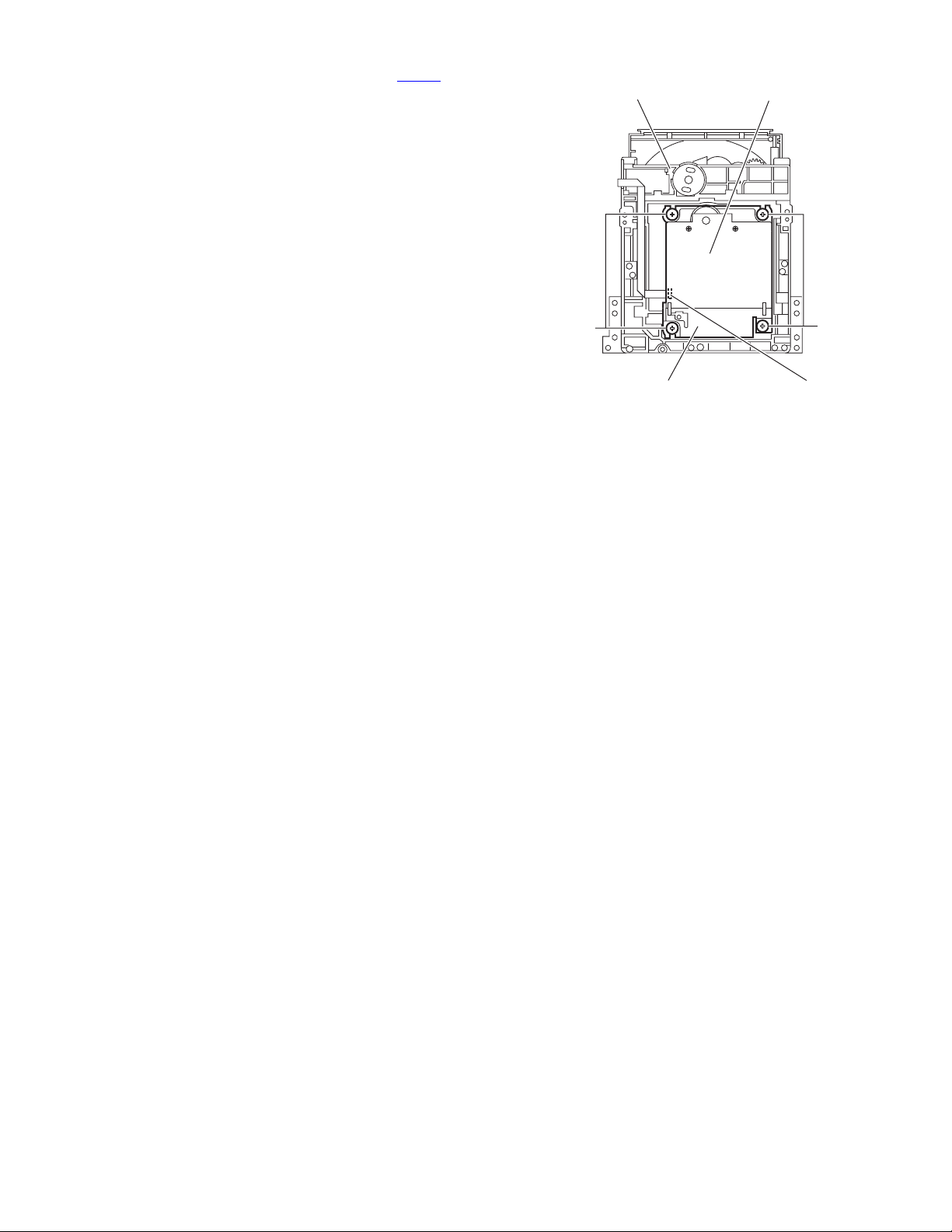
3.1.12 Removing the CD mechanism assembly
(See Figs.20 and 21)
• Prior to performing the following procedures, remove the side
panels L/R, front panel assembly, top cover assembly, tuner,
rear panel, main board and power supply board.
(1) From the top side of the main body, remove the four screws
P attaching the shield case to the bottom chassis. (See
Fig.20.)
Reference:
When attaching the shield case on the bottom chassis,
align the projections (k, m, n) of the bottom chassis in the
holes of the shield case. (See Fig.20.)
(2) Take out the shield case with the power amplifier board
from the bottom chassis.
(3) Remove the three screws Q attaching the CD mechanism
assembly to the bottom chassis. (See Fig.21.)
P
Shield case
k
Bottom chassis
P
m
Power amplifier board
CD mechanism assembly
Bottom chassis
n
P
Fig.20
Q
Q
Fig.21
(No.MB262)1-15
Page 50

3.1.13 Removing the power transformer
(See Figs.22 and 23)
• Prior to performing the following procedures, remove the side
panels L/R, front panel assembly, top cover assembly and rear
panel.
(1) From the forward side of the power supply board, discon-
nect the wires from the connectors (CN102
CN105). (See Fig.22.)
Reference:
Remove the power supply board as required. (See
Fig.17.)
(2) From the top side of the main body, remove the four screws
R attaching the power transformer. (See Fig.23.)
, CN103,
CN102
Power supply board
CN103
CN105
Fig.22
Power transformer
R
R
R
Fig.23
1-16 (No.MB262)
Page 51

3.1.14 Removing the FL board
(See Fig.24)
• Prior to performing the following procedures, remove the side
panels L/R and front panel assembly.
(1) From the inside of the front panel assembly, remove the
four screws S attaching the FL board.
(2) Take out the FL board from the front panel assembly and
disconnect the card wire from the connector CN751
FL board.
Reference:
When attaching the FL board, align the projections p of the
front panel assembly in the holes of the FL board.
on the
CN751
Card
wire
S
FL board
p
S
p
S
S
Front panel assembly
Fig.24
(No.MB262)1-17
Page 52

3.1.15 Removing the switch board
(See Figs.25 and 26)
• Prior to performing the following procedures, remove the side
panels L/R and front panel assembly.
(1) From the front side of the front panel assembly, pull out the
mic volume knob. (See Fig.25.)
(2) From the inside of the front panel assembly, remove the
ten screws T attaching the switch board. (See Fig.26.)
(3) Take out the switch board from the front panel assembly
and disconnect the card wire from the connector CN760
the switch board. (See Fig.26.)
Reference:
When attaching the switch board, align the projections q of the
front panel assembly in the holes of the switch board. (See
Fig.26.)
on
Front panel assembly
Mic volume knob
Fig.25
Card wire
T
Switch board
CN760
q
T
q
T
Fig.26
1-18 (No.MB262)
Page 53

3.1.16 Removing the headphone jack board
(See Fig.27)
• Prior to performing the following procedure, remove the side
panels L/R and front panel assembly.
(1) From the inside of the front panel assembly, remove the
screw U attaching the headphone jack board.
Reference:
After attaching the headphone jack board, fix the wire with the
spacer.
Spacer
Wire
U
Headphone jack board
Fig.27
Front panel assembly
(No.MB262)1-19
Page 54

3.2 CD mechanism section
• Remove the CD mechanism assembly from the main body.
(See "3.1.12 Removing the CD mechanism assembly".)
3.2.1 Removing the tray assembly
(See Figs.1 to 3)
(1) From the right side of the CD mechanism assembly, push
the slide cam and pull the tray assembly out of the CD
mechanism assembly in the direction of the arrow. (See
Fig.1)
(2) From the top side of the CD mechanism assembly, remove
the two screws A attaching the leaf spring to the bushing
and remove the leaf spring. (See Fig.2)
(3) Remove the bushing of the tray assembly from the projec-
tion a on the CD mechanism assembly and move the tray
assembly in the direction of the arrow. (See Fig.3)
(4) Remove the claw b of the tray assembly from the CD
mechanism assembly and take out the tray assembly. (See
Fig.3)
Tray assembly CD mechanism assembly
Slide cam
Fig.1
Leaf spring
Bushing
A
3.2.2 Removing the traverse mechanism assembly
(See Figs.4)
(1) From the bottom side of the CD mechanism assembly, re-
move the four screws B attaching the traverse mechanism
1-20 (No.MB262)
CD mechanism assembly
Projection a
Claw b
CD mechanism assembly
assembly.
Fig.2
Bushing
Tray assembly
Fig.3
Page 55

(2) Disconnect the card wire from the connector CN602
CD servo board and take out the CD traverse mechanism
assembly with the CD servo board.
on the
CD mechanism assembly
CD servo board
B
Traverse mechanism assembly
Fig.4
B
CN602
(No.MB262)1-21
Page 56

3.2.3 Removing the CD servo board
(See Figs.5 and 6)
• Remove the traverse mechanism assembly.
(1) From the bottom side of the traverse mechanism assem-
bly, remove the solders from the solder sections c. (See
Fig.5)
(2) Remove the wire (yellow) from the solder sections d. (See
Fig.5)
(3) Remove the wire (white) from the solder sections e. (See
Fig.5)
(4) Remove the two screws C attaching the CD servo board.
(See Fig.5)
(5) Remove the CD servo board from the claws f in the direc-
tion of the arrow and turn the CD servo board over. (See
Fig.5)
(6) Solder the short land sections g on the CD pickup. (See
Fig.6)
(7) Release the lock of the connector CN601
board in the direction of the arrow and disconnect the card
wire. (See Fig.6)
Caution:
• Solder the short land sections g on the CD pickup before disconnecting the card wire from the connector CN601
CD servo board. If the card wire is disconnected without attaching solder, the CD pickup may be destroyed by static
electricity. (See Fig.6)
• When attaching the CD servo board, be sure to remove solders from the short land sections g after connecting the card
wire to the connector CN601
Fig.6)
on the CD servo board. (See
on the CD servo
on the
Claw f
Solder section c
CD servo board
Wire (yellow)
CC
Wire (white)
Solder
section d
Solder
section e
Claw f
Traverse mechanism assemblyCD servo board
Fig.5
CN601
CD pickup
Short land section g
Lock
Traverse mechanism assembly
Fig.6
1-22 (No.MB262)
Page 57

3.2.4 Removing the CD pickup
(See Figs.7 to 9)
• Remove the traverse mechanism assembly.
(1) From the top side of the traverse mechanism assembly, re-
move the screw D attaching the shaft holder. (See Fig.7)
(2) Release the joint h and take out the shaft holder. (See
Fig.7)
(3) Remove the two screws E attaching the rack arm and take
out the rack arm. (See Fig.8)
(4) Remove the feed middle gear and remove the screw shaft
of the CD pickup from the section i on the traverse mechanism assembly. (See Fig.8)
(5) Remove the CD pickup from the section j of the traverse
mechanism assembly and take out the CD pickup with the
screw shaft. (See fig.8)
(6) Pull the screw shaft out of the CD pickup. (See Fig.8)
(7) From the bottom side of the CD pickup, solder the short
land sections k on the CD pickup. (See Fig.9)
(8) Release the lock of the connector on the CD pickup in the
direction of the arrow and disconnect the card wire. (See
Fig.9)
Caution:
• Solder the short land sections k on the CD pickup before dis-
connecting the card wire from the connector on the CD pickup. If the card wire is disconnected without attaching solder,
the CD pickup may be destroyed by static electricity. (See
Fig.9)
• When attaching the CD pickup, be sure to remove solders
from the short land sections k after connecting the card wire
to the connector on the CD pickup. (See Fig.9)
Traverse mechanism assembly
Feed middle gear
Screw shaft
DJoint h
Shaft holder
Fig.7
Rack arm
E
Section i
CD pickup
Short land section k
CD pickup Connector Card wire
Section j
Fig.8
Fig.9
(No.MB262)1-23
Page 58

3.2.5 Attaching the CD pickup
(See Figs.7 to 10)
• See "3.2.4 Removing the CD pickup".
(1) Remove solders from the short land sections k after con-
necting the card wire to the connector on the CD pickup.
(See Fig.9)
(2) Attach the shaft. (See Fig.8)
(3) Align the CD pickup to the section j of the traverse mecha-
nism assembly first, and set the screw shaft of the CD pick-
up in the sections i of the traverse mechanism assembly.
(See Fig.8.)
(4) Attach the rack arm and feed middle gear. (See Fig.8)
(5) Attach the shaft holder. (See Fig.7)
(6) Turn the SS gear in the direction of the arrow 1 to move the
CD pickup in the direction of the arrow 2. (See Fig.10)
SS gear
1
2
3.2.6 Removing the feed motor
(See Figs.5, 7 and 11)
• Remove the traverse mechanism assembly.
(1) From the top side of the traverse mechanism assembly, re-
move the wire (yellow) from the solder sections d on the
CD servo board. (See Fig.5)
(2) Remove the wire (white) from the solder sections e on the
CD servo board. (See Fig.5)
(3) Remove the screw D attaching the shaft holder and take
out the shaft holder. (See Fig.7)
(4) Remove the feed middle gear and remove the screw E at-
taching the feed motor. (See Fig.11)
(5) Take out the feed motor from the traverse mechanism as-
sembly.
Reference:
When attaching the feed motor, pass the wires through the
section m on the traverse mechanism assembly. (See Fig.11)
Traverse mechanism assembly
Fig.10
E
Feed motor
Wires
Pickup
Section m
1-24 (No.MB262)
Feed middle gear
Traverse mechanism assembly
Fig.11
Page 59

3.2.7 Removing the CD loading switch board
(See Fig.12)
(1) From the bottom side of the CD mechanism assembly, dis-
connect the card wire from the connector CN1
loading switch board.
(2) Remove the wires from the solder section n on the CD
loading switch board.
(3) Lift the CD loading switch board while pressing the claw p
of the CD mechanism assembly in the direction of the arrow and remove it from the section q.
Reference:
• Put the wires on the section r after attaching the CD loading
switch board to the CD mechanism assembly.
• Fix the claw p on the CD mechanism assembly with bonds
after attaching the CD loading switch board.
3.2.8 Removing the motor
(See Figs.12 and 13)
• Remove the tray assembly.
(1) From the bottom side of the CD mechanism assembly, re-
move the wires from the solder section n on the CD loading
switch board. (See Fig.12)
(2) From the top side of the CD mechanism assembly, remove
the belt from the motor pulley. (See Fig.13)
Note:
Take care not to attach grease on the belt.
(3) Remove the two screws F attaching the motor to the CD
mechanism assembly and take out the motor from the bottom side of the CD mechanism assembly. (See Fig.13)
Reference:
Put the wires on the section r after attaching the motor to the
CD mechanism assembly. (See Fig.12)
on the CD
CD loading switch board
Wire
Solder
section n
CN1
section q section r
CD mechanism assembly
F
Claw p
CD mechanism assembly
Fig.12
Belt
Fig.13
Motor pulley
(No.MB262)1-25
Page 60

3.3 Cassette mechanism assembly
3.3.1 Removing the Play/Record & Clear head
(See Fig.1~3)
(1) While moving the trigger arm on the right side of the head
mount in the direction of the arrow, turn the flywheel R
counterclockwise until the head mount comes ahead and
clicks.
(2) The head turns counterclockwise as you turn the flywheel
R counterclockwise (See Fig.2 and 3).
(3) Disconnect the flexible wire from connector CN31
head amplifier & mechanism control board.
(4) Remove the spring from the back of the head.
(5) Loosen the azimuth screw for reversing attaching the head.
(6) Remove the head on the front side of the head mount.
on the
Cassette mechanism assembly
Fig.1
Head
Fly wheelR
Trigger armHead mount
Flexible wire
Fly wheel R
Fig.2
Azimuth screw
Head
for reversing
Spring
CN31
Head amplifer & mecha control board
Fig.3
1-26 (No.MB262)
Page 61

3.3.2 Removing the head amplifier & mechanism control board
(See Fig.4)
(1) Turn over the cassette mechanism assembly and remove
the three screws A attaching the head amplifier & mechanism control board.
(2) Disconnect the flexible wire from connector CN31
head amplifier & mechanism control board.
(3) Disconnect connector CN32
anism control board from connector CN1
board.REFERENCE: If necessary, unsolder the 4-pin wire
soldered to the main motor.
3.3.3 Removing the main motor
(See Fig.4~7)
(1) Remove the two screws B .
(2) Half raise the motor and remove the capstan belt from the
motor pulley.
ATTENTION:
Be careful to keep the capstan belt from grease. When reassembling, refer to Fig.6 and 7 for attaching the capstan belt.
Head amplifier & mecha control board
of the head amplifier & mech-
on the reel pulse
on the
Main motor assembly
Capstan belt
Fig.5
Main motor assembly
CN31
Flexible wire
A
AA
Fig.4
CN32
4pin wire
B
Main motor assembly
Motor pulley
Capstan belt
Fig.6
Main motor assembly
Fly wheel
Capstan belt
Motor pulley
Fig.7
(No.MB262)1-27
Page 62

3.3.4 Removing the flywheel
(See Fig.8, 9)
• Prior to performing the following procedure, remove the head
amplifier & mechanism control board and the main motor assembly.
(1) From the front side of the cassette mechanism, remove the
slit washers attaching the capstan shaft L and R. Pull out
the flywheels backward.
Fly wheel R Fly wheel L
Fig.8
Fly wheel R
Capstan shaft R Capstan shaft L
Slit washer
Fig.9
3.3.5 Removing the reel pulse board and solenoid
(See Fig.10)
• Prior to performing the following procedure, remove the head amplifier & mechanism control board.
(1) Remove the screw C.
(2) Release the tab a, b, c, d and e retaining the reel pulse board.
(3) Release the tab f and g attaching the solenoid on the reel pulse board.
(4) The reel pulse board and the solenoid come off.
Fly wheel L
bc
a
Solenoid
g
f
d
Reel pulse board
C
e
Fig.10
1-28 (No.MB262)
Page 63

3.3.6 Reattaching the Play/ Record & Clear head
r
r
(See Fig.11~13)
(1) Reattaching the head mount assembly.
a) Change front of the direction cover of the head
mount assembly to the left (Turn the head forward).
b) Fit the bosses O', P', Q', U' and V' on the head mount
assembly to the holes P and V, the slots O, U and Q
of the mechanism sub assembly (See Fig.11 to 13).
CAUTION:
To remove the head mount assembly, turn the direction
cover to the left to disengage the gear. If the gear can not
be disengaged easily, push up the boss Q' slightly and
raise the rear side of the head mounts slightly to return
the direction lever to the reversing side.
(2) Tighten the azimuth screw for reversing.
(3) Reattach the spring from the back of the Play/ Record &
Clear head.
(4) Connect the flexible wire to connector CN31
amplifier & mechanism control board.
on the head
U' Q'
Head mount assembly
Head mount assembly
O'
Fig.11
P'
P'
V'
V'
Direction cove
Spring
Flexible wire
V
O
P
Q
Head
Direction cove
U
Fig.12
Azimuth screw for reversing
Head mount
CN31
Fig.13
Head amplifier &
mechanism control board
(No.MB262)1-29
Page 64

4.1 Jigs and test instruments
• Remote controller
4.2 Adjustment and check method
4.2.1 Initialize all data to the factory setting
SECTION 4
ADJUSTMENT
4.2.4 Fan motor ON/OFF check
Pressing the [STOP] , [SLEEP] and
[STANDBY/ON] together at Power
ON condition.
FL indication
COLD
Initialize is complete.
4.2.2 Confirmation of the system micro computer
Pressing the [STOP] , [SLEEP] and
[STANDBY/ON] together at Power
ON condition.
FL indication
08 02 E
or
09 00 E
Setup is complete.
Pressing the [STOP] , [SLEEP] and
[STANDBY/ON] together at Power
ON condition.
Fan motor is rotating.
Setup is complete.
4.2.3 FL all lighting-up check
Pressing the [STOP] , [SLEEP] and
[STANDBY/ON] together at Power
ON condition.
FL indication
All of the FL displays light up.
Setup is complete.
1-30 (No.MB262)
Page 65

TROUBLE SHOOTING
5.1 Flow of functional operation untill TOC read (CD)
Power ON
Disc play Key
Automatic tuning of FO offset and TE offset
SECTION 5
Slider turns REST
SW ON.
Laser ON
Detection of disc
Check Point
Confirm that the voltage at
the pin68 of IC251 is 0V.
(ON: 0V)
Tracking error waveform at TOC reading
IC601
20pin(TEOUT)
Approx.
1.4V
VREF
Disc status
to rotate
Approx. 3sec
Tracking
servo
off status
Automatic measurement
of TE amplitude and
automatic tuning of TE
balance
Tracking
servo
on status
Disc to be
braked to stop
TOC reading
finishes
500mv/div
2ms/div
Fig.1
Automatic measurement of
Focus S-curve amplitude
Disc is rotated
Focus servo ON
(Tracking servo ON)
Automatic measurement of
Tracking error amplitude
Automatic tuning of
Tracking error balance
Automatic tuning of
Focus error balance
Automatic tuning of
Focus error gain
Confirm that the Focus error
S-curve signal at the pin32 of
IC651 is approx. 1.4Vp-p.
Confirm that the signal from
pin22 of IC651 is 0V as a accelerated
pulse during approx. 640ms.
Confirm the waveform of the
Tracking error signal at the
pin20 of IC601(one side of
R604) (See Fig.1.)
Automatic tuning of
Tracking error gain
TOC reading
Play a disc
Confirm the eye-pattern
at the pin5 of IC601
(No.MB262)1-31
Page 66

5.2 Maintenance of laser pickup (CD)
(1) Cleaning the pick up lens
Before you replace the pick up, please try to clean the lens
with a alcohol soaked cotton swab.
(2) Life of the laser diode
When the life of the laser diode has expired, the following
symptoms will appear.
• The level of RF output (EFM output : ampli tude of eye
pattern) will below.
5.3 Replacement of laser pickup (CD)
Turn of the power switch and, disconnect the
power cord.
Replace the pickup with a normal one. (Refer
to "Pickup Removal" on the previous page)
Is RF output
0.9 0.22Vp-p?
NO
Replace it.
YES
O.K
(3) Semi-fixed resistor on the APC PC board
The semi-fixed resistor on the APC printed circuit board
which is attached to the pickup is used to adjust the laser
power. Since this adjustment should be performed to
match the characteristics of the whole optical block, do not
touch the semi-fixed resistor.
If the laser power is lower than the specified value, the laser diode is almost worn out, and the laser pickup should
be replaced.
If the semi-fixed resistor is adjusted while the pickup is
functioning normally, the laser pickup may be damaged
due to excessive current.
Plug the power cord in, and turn the power on.
At this time, check that the laser emits for
about 3 seconds and the objective lens moves
up and down.
Note: Do not observe the laser beam directly.
Play a disc.
Check the eye-pattern at 5pin of IC601.
Finish.
1-32 (No.MB262)
Page 67

(No.MB262)1-33
Page 68

Victor Company of Japan, Limited
AV & MULTIMEDIA COMPANY AUDIO/VIDEO SYSTEMS CATEGORY 10-1,1chome,Ohwatari-machi,Maebashi-city,371-8543,Japan
(No.MB262)
Printed in Japan
WPC
Page 69

PARTS LIST
[ UX-P400 ]
* All printed circuit boards and its assemblies are not available as service parts.
Area suffix
US ---------------------- Singapore
UF ---------------------------- China
UP ---------------------------- Korea
UT --------------------------- Taiwan
UW ---------- Brazil,Mexico,Peru
- Contents -
Exploded view of general assembly and parts list (Block No.M1)
Speaker assembly and parts list (US,UP,UT,UW) (Block No.M2)
CD mechanism assembly and parts list (Block No.MB)
Cassette mechanism assembly and parts list (Block No.MP)
Electrical parts list (Block No.01~06)
Packing materials and accessories parts list (Block No.M3)
No. MB262 3-1
3- 2
3- 6
3- 7
3- 9
3-11
3-18
Page 70

Exploded view of general assembly and parts list
2
92
77
Block No.
M
M
1
M
60
58
4
71
B
A
74
E
G
57
D
81
62
67
F
59
j
64
82
50
61
69
H
i
K
68
37
FL board
14
65
22
84
L
66
k
10
27
68
DI750
23
32
76
26
30
25
H
16
70
1
18
E
5
3
F
70
15
4
18
21
8
85
16
Switch board
6
21
2
12
20
m
3-2
75
17
J
19
7
36
Headphone jack board
19
Page 71

58
42
Power supply board
43
39
41
40
38
d
e
f
p
K
80
i
86
79
c
78
91
45
Power amplifier board
63
b
48
47
83
63
K
37
L
e
d
88
33
37
L
33
49
40
51
54
A
B
h
G
89
52
90
C
56
52
55
D
g
53
46
30
26
37
35
30
a
34
k
c
b
m
Main board
44
g
h
i
j
a
11
73
C
44
13
72
32
87
28
f
29
31
p
24
J
25
J
3-3
Page 72

General assembly
Block No. [M][1][M][M]
Symbol No. Part No. Part Name Description Local
1 GV10189-015A FRONT PANEL
2 GV30569-003A FRONT LENS
3 GV40470-001A STANDBY LENS
4 GV40471-001A REMOTE LENS
5 GV20265-001A MAIN BUTTON
6 GV40472-001A EJECT BUTTON
7 GV30555-002A VOL PLATE
8 GV40473-002A LCD LENS
10 GV30557-001A LCD HOLDER
11 E70945-H40B HEAT SINK
12 GV40478-003A LED LENS
13 QYSBSG3008Z TAP SCREW M3 x 8mm
14 GV30616-001A SHIELD P400UP
15 GV40203-002A LED HOLDER
16 QYSBSF2608Z TAP SCREW M2.6 x 8mm(x10)
17 GV40035-001A SPECIAL SCREW
18 QYSDSF2006M TAP SCREW M2 x 6mm(x4)
19 GV40313-002A FELT SPACER (x2)
20 GV30349-007A SPACER
21 QYSBSF2606Z TAP SCREW M2.6 x 6mm(x3)
22 QYSBSF2608Z TAP SCREW M2.6 x 8mm(x4)
23 GV10190-001A BOTTOM CHASSIS
24 GV40313-002A FELT SPACER (x2)
25 GV40474-001A MECHA HOLDER F (x2)
26 GV40479-001A MECHA HOLDER R
27 GV20269-002A SHIELD CASE
28 E3400-444 FELT SPACER
29 GV40242-004A COMMON SPACER
30 QYSDST3005Z TAP SCREW M3 x 5mm(x2)
31 QYSDST3005Z TAP SCREW M3 x 5mm(x2)
32 QYSBSF3008Z TAP SCREW M3 x 8mm(x3)
33 QYSBST4006Z TAP SCREW M4 x 6mm(x4)
34 QMPR480-200-JC POWER CORD(EU) 2m BLACK P400UF
34 QMPR310-200-JC POWER CORD(EU) 2m BLACK P400UP
34 QMPR600-200-JD POWER CORD(EU) 2m BLACK P400UT
34 QMPK200-200-JD POWER CORD(EU) 2m BLACK P400US,P400UW
35 QZW0033-001 STRAIN RELIEF
36 QYSSST3008Z TAP SCREW M3 x 8mm(x2)
37 QYSDST3005Z TAP SCREW M3 x 5mm(x4)
38 GV40480-002A IC HOLDER
39 GV30559-007A HEAT SINK P400US,P400UT,P400UW
40 QYSBST3006E TAP SCREW M3 x 6mm(x2)
41 QYSBSG3012Z TAP SCREW M3 x 12mm(x2)
42 QYSBSTG3006Z TAP SCREW M3 x 6mm
43 QYSBSTG3006Z TAP SCREW M3 x 6mm
44 QYSBSTG3006Z TAP SCREW M3 x 6mm(x2)
45 QYSBST3006E TAP SCREW M3 x 6mm(x2)
46 GV20270-033A REAR PANEL P400UF,P400UP
46 GV20270-035A REAR PANEL P400US,P400UT,P400UW
47 QAU0347-001 TUNER P400UP
47 QAU0346-001 TUNER TU 1 P400UF,P400US,P400UT,P400UW
48 GV40481-001A FAN BRACKET
49 QAR0230-001 FAN
50 LV41843-002A LASER CAUTION
51 QYSBSGY3008E TAP SCREW M3 x 8mm(x2)
52 QYSBSGY3008E TAP SCREW M3 x 8mm(x2)
53 QYSBSGY3008E TAP SCREW M3 x 8mm(x2)
54 QYSBSGY3008E TAP SCREW M3 x 8mm
55 QYSBSGY3008E TAP SCREW M3 x 8mm
56 QYSBSGY3008E TAP SCREW M3 x 8mm(x2) P400US,P400UT,P400UW
57 GV20288-003A TOP COVER ASSY
58 GV40506-001A DOOR SPRING
59 GV40034-001A DAMPER ASSY.
60 GV40220-001A LACH
61 VKL7850-002 EJECT SAFTY(R)
62 VKW5258-003 TORSION SPRING
63 GV30349-022A SPACER (x2)
64 GV40229-001A SUPPORT BRACKET
65 GV30071-001A HEAD SHIELD
66 QYSBSF2608Z TAP SCREW M2.6 x 8mm(x2)
67 QYSBSF3008Z TAP SCREW M3 x 8mm
68 QYSBSF3010Z TAP SCREW M3 x 10mm(x4)
69 GV40035-001A SPECIAL SCREW
70 QYSSSF3008Z TAP SCREW M3 x 8mm(x2)
3-4
Page 73

Symbol No. Part No. Part Name Description Local
71 GV10194-004A SIDE PANEL L
72 GV10195-001A SIDE PANEL R
73 QYSBSGY3010E TAP SCREW M3 x 10mm(x2)
74 QYSBSGY3010E TAP SCREW M3 x 10mm(x2)
75 GV30563-001A MIC VOL KNOB
76 GV30564-003A TRAY FITTING
77 GV30565-002A RATING LABEL P400UF
77 GV30565-006A RATING LABEL P400US,P400UT,P400UW
78 QMF51W2-R63-J8 FUSE F 1001 P400UF,P400UP
78 QMF51W2-1R25-J8 FUSE F 1001 P400US,P400UT,P400UW
79 QMF51W2-1R25-J8 FUSE F 1003
80 QMF51W2-6R3-J8 FUSE F 1005
81 QUQH12-0922AJ CARD WIRE
82 QUQH12-1022AJ CARD WIRE
83 QUQH12-1113AJ CARD WIRE FC 1
84 QUQH12-1508AJ CARD WIRE
85 QUQH12-1008AJ CARD WIRE
86 QUQH12-1114AJ CARD WIRE
87 QUQM10-1716AJ CARD WIRE
88 QQT0426-002 POWER TRANSF P400UF,P400UP
88 QQT0426-003 POWER TRANSF P400US,P400UT,P400UW
89 LV43268-001A CCC LABEL P400UF
90 E70891-001 CLASS 1 LABEL P400UP,P400UT
91 QMF51W2-R63-J8 FUSE F 1002 P400US,P400UT,P400UW
92 GV30497-017A UT LABEL P400UT
92 GV30230-010A UP LABEL P400UP
3-5
Page 74

Speaker assembly and parts list
(US,UP,UT,UW)
Block No.
Block No.
M
M
2
2
M
M
M
M
6
3
4
1
2
5
Speaker (US,UP,UT,UW)
Symbol No. Part No. Part Name Description Local
1 UP4-BK-00-01 SARAN BOARD (x2)
2 UP4-MK-00-01 MARK (x2)
3 UP4-WO-00-01 CONE SPEAKER (x2)
4 UP4-ML-00-01 TAPPING SCREW (x8)
5 UP4-JD-00-01 RUBBER MAT (x8)
6 UP4-HT-02-01 RATING LABEL (x2)
Block No. [M][2][M][M]
3-6
Page 75

CD mechanism assembly and parts list
FMU-ST1-1M
Grease
JVG-31N
JVS-1003
FL-7750E
9
7
4
Block No.
M
M
B
M
8
5
1
36
15
16
12.0mm 0.1mm
22
18
21
18mm 0.1mm
Backside
35
0.10mm
3
2
6
34
b
c
32
28
19
13
12
11
7.95mm
A
27
10
a
26
25
20
31
30
31
30
a
33
b
Switch board
c
31
29
31
29
14
A
3.5mm 0.1mm
17
24
23
3-7
Page 76

CD mechanism
Block No. [M][B][M][M]
Symbol No.
1 LE10283-014A LOADER SUB ASSY
2 QAR0197-001 MOTOR
3 LV42087-002A MOTOR PULLEY
4 QYSPSPU1730Z SCREW M1.7 x 3mm(x2)
5 LE40897-001A BELT
6 LV34586-001A CD CLAMPER
7 LV42930-003A P.C.MAGNET
8 LE40899-001A YOKE
9 LV41741-001A SPECIAL SCREW
10 OPTIMA-725B2 CD PICK UP
11 LV34564-001A RACK ARM
12 QYSPSPT1720M SCREW M1.7 x 2mm(x2)
13 LV31744-001A P.S.SPRING
14 QYSPSGT1425M TAP SCREW 1.4mm x 2.5mm
15 LV10855-001A TM CHASSIS
16 LV43468-001A T.T ASSY
17 QAR0302-001 SPINDLE MOTOR
18 VKZ4743-001 SPECIAL SCREW (x2)
19 LV40157-001A SCREW SHAFT
20 LV43651-001A SS GEAR
21 LV43650-001A F MOTOR GEAR
22 QAR0303-001 FEED MOTOR
23 QYSPSPT2030M SCREW M2 x 3mm
24 LV34565-002A F MIDDLE GEAR
25 LV34563-001A SHAFT HOLDER
26 QYSPSFT1740Z TAP SCREW M1.7 x 4mm
27 QUQ105-1506BB FFC
28 LV43805-001A FFC
29 LE40900-003A INSULATOR (x2)
30 LE40900-004A INSULATOR (x2)
31 LE40901-001A SPECIAL SCREW (x4)
32 QYSBSF2006Z TAP SCREW M2 x 6mm(x2)
33 VYSH101-034 SPACER
34 LV30225-096A SPACER
35 LV30225-073A SPACER
36 LV43828-001A SPACER
Part No. Part Name Description Local
3-8
Page 77

Cassette mechanism assembly and parts list
Grease
= EM-30L
=UD-24
=LEN-320M
=MOBIL-1
1
34
27
3
13
Block No.
SLC-S303M
8
15
2
16
14
C
9
11
1
12
23
2
3
10
4
7
29
M
M
M
P
6
5
The lower side
B
A
19
24
5
6
Switch board
30
25
31
22
17
C
36
11
18
21
28
20
26
A
32
33
B
Head amplifier
board
35
35
33
32
0.1
0.15 mm
_
+
8.7
3-9
Page 78

Cassette mechanism
Block No. [M][P][M][M]
Symbol No.
1 VKS1165-00N CHASSIS B. ASSY
2 VKS2274-002 REEL GEAR (x2)
3 VKW5286-002 B.T. SPRING (x2)
4 VKS5559-001 PLAY IDLE GEAR
5 VKS5595-002 BLIND
6 VKS5560-003 FR IDLE GEAR
7 LV42013-001A EARTH SPRING
8 SLC303HMB-1 HEAD MOUNT ASSY
9 VKY3149-002 CASSETTE SP.
10 LV31786-002A PLAY LEVER
11 VKS1166-003 CONTROL CAM
12 VKW5279-002 HEAD BASE SP(R)
13 VKW5280-001 HEAD BASE SP(L)
14 LV41584-001A BRAKE(R)
15 LV41585-003A BRAKE(L)
16 QYSBSF2005Z SCREW 2mm x 5mm
17 VKS5603-00G MAIN PULLEY ASS
18 VKS3785-001MM FR ARM
19 VKW5284-002 SWING SPRING
20 VKS2278-003 TRIGGER ARM
21 VKW5301-001 FR SPRING
22 VKW5266-001 ELEVATOR SPRING
23 WDL214025 WASHER
24 QYSBSF2005Z SCREW 2mm x 5mm
25 VKS3786-00G CLUTCH ASSY
26 VKF3205-00B F.WHEEL ASSY(R)
27 WDL183425 SLIT WASHER
28 VKF3207-00C F.WHEEL ASSY(L)
29 WDL173525-6 SLIT WASHER
30 VKZ3174-00B DC SOLENOID
31 LV42836-001A CAPSTAN BELT
32 QAR0309-001 D.C.MOTOR
33 VKR4761-003 MOTOR PULLEY
34 QYSPSP2604Z SCREW 2.6mm x 4mm(x2)
35 QYSBSF2608Z TAPPING SCREW 2.6mm x 8mm(x3)
36 QUQH12-0906BF WIRE
Part No. Part Name Description Local
3-10
Page 79

Electrical parts list
Main board
Block No. [0][1][0][0]
Symbol No.
IC200 LC75342M-X IC
IC202 JCV8011-X IC
IC240 KIA7810API IC
IC241 PQ033RD01SZ IC
IC701 MN101C49GFL2 MASK ROM
IC703 BD4740G-W IC
IC705 KIA78S06P-T IC
Q2200 2SC3576-JVC-T TRANSISTOR
Q2220 2SD601A/R/-X TRANSISTOR
Q2221 UN2111-X TRANSISTOR
Q2410 KTC2026/Y/ TRANSISTOR
Q7001 UN2214-X TRANSISTOR
Q7002 UN2215-X TRANSISTOR
Q7146 UN2215-X TRANSISTOR
Q7154 2SD601A/R/-X TRANSISTOR
Q7158 2SD601A/R/-X TRANSISTOR
Q7161 UN2211-X TRANSISTOR
Q7162 UN2211-X TRANSISTOR
Q7246 UN2211-X TRANSISTOR
Q7300 2SB709A/RS/-X TRANSISTOR
Q7301 UN2215-X TRANSISTOR
Q7302 KRC110M-T TRANSISTOR
Q7320 2SB709A/RS/-X TRANSISTOR
Q7321 UN2215-X TRANSISTOR
Q7340 2SD601A/R/-X TRANSISTOR
Q7360 2SB709A/RS/-X TRANSISTOR
Q7361 UN2215-X TRANSISTOR
D2400 MTZJ11C-T2 Z DIODE
D2401 1SS133-T2 DIODE
D2402 1N4003S-T5 SI DIODE
D2403 1N4003S-T5 SI DIODE
D2410 MTZJ3.9B-T2 Z DIODE
D2411 1SS133-T2 DIODE
D2413 MTZJ6.8C-T2 Z DIODE
D7001 1SS133-T2 DIODE
D7002 1SS133-T2 DIODE
D7003 MTZJ5.1A-T2 Z DIODE
D7062 1SS133-T2 DIODE
D7161 1SS133-T2 DIODE
D7300 1SS133-T2 DIODE
D7301 1SS133-T2 DIODE
D7320 1SS133-T2 DIODE
D7340 1N4003S-T5 SI DIODE
D7341 1SS133-T2 DIODE
D7350 MTZJ6.2C-T2 Z DIODE
D7351 1SS133-T2 DIODE
D7352 1SS133-T2 DIODE
D7353 1SS133-T2 DIODE
D7354 1SS133-T2 DIODE
C2000 QCBB1HK-221Y C CAPACITOR 220pF 50V K
C2001 QETN1HM-475Z E CAPACITOR 4.7uF 50V M
C2002 QETN1HM-475Z E CAPACITOR 4.7uF 50V M
C2003 QTE1H28-106Z E CAPACITOR 10uF 50V
C2004 QETN1HM-475Z E CAPACITOR 4.7uF 50V M
C2006 QTE1E28-106Z E CAPACITOR 10uF 25V
C2007 QTE1E28-106Z E CAPACITOR 10uF 25V
C2008 QFLC1HJ-272Z M CAPACITOR 2700pF 50V J
C2009 QFLC1HJ-104Z M CAPACITOR 0.1uF 50V J
C2010 QFLC1HJ-104Z M CAPACITOR 0.1uF 50V J
C2016 QTE1H28-105Z E CAPACITOR 1uF 50V
C2021 QTE1H28-106Z E CAPACITOR 10uF 50V
C2023 QTE1H28-106Z E CAPACITOR 10uF 50V
C2032 QFLC1HJ-222Z M CAPACITOR 2200pF 50V J
C2080 QCFB1HZ-104Y C CAPACITOR 0.1uF 50V Z
C2081 QDXB1CM-332Y C CAPACITOR 3300pF 16V M
C2100 QCBB1HK-221Y C CAPACITOR 220pF 50V K
C2101 QETN1HM-475Z E CAPACITOR 4.7uF 50V M
C2102 QETN1HM-475Z E CAPACITOR 4.7uF 50V M
C2103 QTE1H28-106Z E CAPACITOR 10uF 50V
Part No. Part Name Description Local
Symbol No.
C2104 QETN1HM-475Z E CAPACITOR 4.7uF 50V M
C2106 QTE1E28-106Z E CAPACITOR 10uF 25V
C2107 QTE1E28-106Z E CAPACITOR 10uF 25V
C2108 QFLC1HJ-272Z M CAPACITOR 2700pF 50V J
C2109 QFLC1HJ-104Z M CAPACITOR 0.1uF 50V J
C2110 QFLC1HJ-104Z M CAPACITOR 0.1uF 50V J
C2116 QTE1H28-105Z E CAPACITOR 1uF 50V
C2121 QTE1H28-106Z E CAPACITOR 10uF 50V
C2122 QETN1HM-106Z E CAPACITOR 10uF 50V M
C2123 QTE1H28-106Z E CAPACITOR 10uF 50V
C2132 QFLC1HJ-222Z M CAPACITOR 2200pF 50V J
C2180 QCFB1HZ-104Y C CAPACITOR 0.1uF 50V Z
C2181 QDXB1CM-332Y C CAPACITOR 3300pF 16V M
C2200 QTE1C06-107Z E CAPACITOR 100uF 16V
C2201 QFLC1HJ-104Z M CAPACITOR 0.1uF 50V J
C2202 QTE1C06-107Z E CAPACITOR 100uF 16V
C2203 QCBB1HK-103Y C CAPACITOR 0.01uF 50V K
C2204 QETN1HM-226Z E CAPACITOR 22uF 50V M
C2220 QTE1C06-476Z E CAPACITOR 47uF 16V
C2221 QETN1CM-476Z E CAPACITOR 47uF 16V M
C2222 QFLC1HJ-273Z M CAPACITOR 0.027uF 50V J
C2223 QETN1HM-475Z E CAPACITOR 4.7uF 50V M
C2224 QETN1CM-106Z E CAPACITOR 10uF 16V M
C2225 QETN1HM-106Z E CAPACITOR 10uF 50V M
C2226 QETN1HM-475Z E CAPACITOR 4.7uF 50V M
C2227 QETN1HM-106Z E CAPACITOR 10uF 50V M
C2228 QETN1HM-106Z E CAPACITOR 10uF 50V M
C2229 QETN1HM-224Z E CAPACITOR 0.22uF 50V M
C2230 QETN1HM-475Z E CAPACITOR 4.7uF 50V M
C2231 QETN1HM-684Z E CAPACITOR 0.68uF 50V M
C2232 QETN1HM-475Z E CAPACITOR 4.7uF 50V M
C2233 QETN1CM-476Z E CAPACITOR 47uF 16V M
C2274 QETN1CM-107Z E CAPACITOR 100uF 16V M
C2280 QCBB1HK-101Y C CAPACITOR 100pF 50V K
C2282 QCBB1HK-101Y C CAPACITOR 100pF 50V K
C2400 QETN1EM-477Z E CAPACITOR 470uF 25V M
C2401 QETN1CM-227Z E CAPACITOR 220uF 16V M
C2410 QETN1CM-107Z E CAPACITOR 100uF 16V M
C2411 QETN1CM-227Z E CAPACITOR 220uF 16V M
C2412 QETN1EM-107Z E CAPACITOR 100uF 25V M
C2413 QFLC1HJ-104Z M CAPACITOR 0.1uF 50V J
C2414 QETN1EM-107Z E CAPACITOR 100uF 25V M
C7001 QETN1CM-107Z E CAPACITOR 100uF 16V M
C7002 QDYB1CM-103Y C CAPACITOR 0.01uF 16V M
C7004 QETN1HM-225Z E CAPACITOR 2.2uF 50V M
C7005 NCB31HK-223X C CAPACITOR 0.022uF 50V K
C7006 NCB31HK-102X C CAPACITOR 1000pF 50V K
C7007 NCB31HK-103X C CAPACITOR 0.01uF 50V K
C7008 QETN1CM-227Z E CAPACITOR 220uF 16V M
C7009 QETN0JM-228Z E CAPACITOR 2200uF 6.3V M
C7103 NCB31HK-102X C CAPACITOR 1000pF 50V K
C7112 NCS31HJ-330X C CAPACITOR 33pF 50V J
C7113 NCS31HJ-330X C CAPACITOR 33pF 50V J
C7180 QCBB1HK-151Y C CAPACITOR 150pF 50V K
C7181 QDGB1HK-102Y C CAPACITOR 1000pF 50V K
C7182 QCBB1HK-101Y C CAPACITOR 100pF 50V K
C7320 QETN1HM-106Z E CAPACITOR 10uF 50V M
C7340 NCB31HK-103X C CAPACITOR 0.01uF 50V K
C7350 QFLC1HJ-104Z M CAPACITOR 0.1uF 50V J
C7351 QETN1CM-476Z E CAPACITOR 47uF 16V M
C7352 QETN1CM-107Z E CAPACITOR 100uF 16V M
C7353 QETN1CM-107Z E CAPACITOR 100uF 16V M
C7367 QETN1CM-476Z E CAPACITOR 47uF 16V M
C7371 QCBB1HK-561Y C CAPACITOR 560pF 50V K
C7372 QCBB1HK-561Y C CAPACITOR 560pF 50V K
R2000 QRE141J-303Y C RESISTOR 30kΩ 1/4W J
R2001 QRE141J-303Y C RESISTOR 30k
R2002 QRE141J-912Y C RESISTOR 9.1k
R2003 QRE141J-222Y C RESISTOR 2.2kΩ 1/4W J
R2004 NRSA63J-622X MG RESISTOR 6.2k
R2006 NRSA63J-472X MG RESISTOR 4.7k
R2007 NRSA63J-392X MG RESISTOR 3.9kΩ 1/16W J
R2008 QRE141J-102Y C RESISTOR 1k
Part No. Part Name Description Local
Ω
1/4W J
Ω
1/4W J
Ω
1/16W J
Ω
1/16W J
Ω
1/4W J
3-11
Page 80

Symbol No.
Part No. Part Name Description Local
Symbol No.
Part No. Part Name Description Local
R2010 QRE141J-273Y C RESISTOR 27kΩ 1/4W J
R2012 NRSA63J-203X MG RESISTOR 20kΩ 1/16W J
R2013 QRE141J-222Y C RESISTOR 2.2kΩ 1/4W J
R2020 NRSA63J-153X MG RESISTOR 15kΩ 1/16W J
R2021 NRSA63J-103X MG RESISTOR 10kΩ 1/16W J
R2022 NRSA63J-432X MG RESISTOR 4.3k
R2079 NRSA63J-471X MG RESISTOR 470
R2100 QRE141J-303Y C RESISTOR 30kΩ 1/4W J
R2101 QRE141J-303Y C RESISTOR 30kΩ 1/4W J
R2102 QRE141J-912Y C RESISTOR 9.1kΩ 1/4W J
R2103 QRE141J-222Y C RESISTOR 2.2kΩ 1/4W J
R2104 NRSA63J-622X MG RESISTOR 6.2kΩ 1/16W J
R2106 NRSA63J-472X MG RESISTOR 4.7kΩ 1/16W J
R2107 QRE141J-392Y C RESISTOR 3.9kΩ 1/4W J
R2108 QRE141J-102Y C RESISTOR 1kΩ 1/4W J
R2112 NRSA63J-203X MG RESISTOR 20kΩ 1/16W J
R2113 QRE141J-222Y C RESISTOR 2.2kΩ 1/4W J
R2120 NRSA63J-153X MG RESISTOR 15kΩ 1/16W J
R2121 NRSA63J-103X MG RESISTOR 10kΩ 1/16W J
R2122 NRSA63J-432X MG RESISTOR 4.3kΩ 1/16W J
R2179 NRSA63J-471X MG RESISTOR 470
R2200 QRE141J-471Y C RESISTOR 470
R2201 QRE141J-101Y C RESISTOR 100Ω 1/4W J
R2202 NRSA63J-101X MG RESISTOR 100Ω 1/16W J
R2203 NRSA63J-101X MG RESISTOR 100Ω 1/16W J
R2220 NRSA63J-334X MG RESISTOR 330kΩ 1/16W J
R2221 NRSA63J-334X MG RESISTOR 330kΩ 1/16W J
R2222 NRSA63J-101X MG RESISTOR 100Ω 1/16W J
R2223 NRSA63J-225X MG RESISTOR 2.2MΩ 1/16W J
R2224 NRSA63J-153X MG RESISTOR 15kΩ 1/16W J
R2225 QRE141J-682Y C RESISTOR 6.8kΩ 1/4W J
R2226 NRSA63J-562X MG RESISTOR 5.6kΩ 1/16W J
R2227 NRSA63J-392X MG RESISTOR 3.9kΩ 1/16W J
R2228 QRE141J-392Y C RESISTOR 3.9kΩ 1/4W J
R2229 QRE141J-101Y C RESISTOR 100Ω 1/4W J
R2410 QRE141J-152Y C RESISTOR 1.5kΩ 1/4W J
R2411 QRE141J-103Y C RESISTOR 10kΩ 1/4W J
R2710 QRE141J-151Y C RESISTOR 150Ω 1/4W J
R2711 QRE141J-151Y C RESISTOR 150Ω 1/4W J
R7001 NRSA63J-223X MG RESISTOR 22kΩ 1/16W J
R7002 NRSA63J-472X MG RESISTOR 4.7kΩ 1/16W J
R7003 NRSA63J-102X MG RESISTOR 1kΩ 1/16W J
R7004 NRSA63J-103X MG RESISTOR 10kΩ 1/16W J
R7005 NRSA63J-681X MG RESISTOR 680Ω 1/16W J
R7006 NRSA63J-681X MG RESISTOR 680Ω 1/16W J
R7045 NRSA63J-472X MG RESISTOR 4.7kΩ 1/16W J
R7046 NRSA63J-104X MG RESISTOR 100kΩ 1/16W J
R7049 NRSA63J-472X MG RESISTOR 4.7kΩ 1/16W J
R7060 NRSA63J-393X MG RESISTOR 39kΩ 1/16W J
R7061 NRSA63J-472X MG RESISTOR 4.7k
R7062 NRSA63J-472X MG RESISTOR 4.7kΩ 1/16W J
R7102 QRE141J-222Y C RESISTOR 2.2k
R7103 QRE141J-222Y C RESISTOR 2.2k
R7104 QRE141J-222Y C RESISTOR 2.2kΩ 1/4W J
R7105 NRSA63J-103X MG RESISTOR 10k
R7106 QRE141J-103Y C RESISTOR 10k
R7107 QRE141J-222Y C RESISTOR 2.2kΩ 1/4W J
R7108 QRE141J-222Y C RESISTOR 2.2k
R7109 QRE141J-103Y C RESISTOR 10kΩ 1/4W J
R7118 QRE141J-102Y C RESISTOR 1k
R7119 QRE141J-222Y C RESISTOR 2.2k
R7120 QRE141J-102Y C RESISTOR 1kΩ 1/4W J
R7121 NRSA63J-102X MG RESISTOR 1k
R7122 NRSA63J-222X MG RESISTOR 2.2k
R7123 NRSA63J-102X MG RESISTOR 1kΩ 1/16W J
R7124 NRSA63J-222X MG RESISTOR 2.2k
R7125 NRSA63J-222X MG RESISTOR 2.2k
R7126 QRE141J-103Y C RESISTOR 10k
R7127 NRSA63J-222X MG RESISTOR 2.2k
R7128 NRSA63J-222X MG RESISTOR 2.2kΩ 1/16W J
R7129 NRSA63J-222X MG RESISTOR 2.2k
R7131 NRSA63J-103X MG RESISTOR 10k
R7132 NRSA63J-103X MG RESISTOR 10kΩ 1/16W J
R7135 NRSA63J-222X MG RESISTOR 2.2k
R7136 NRSA63J-222X MG RESISTOR 2.2k
R7145 NRSA63J-222X MG RESISTOR 2.2kΩ 1/16W J
R7146 NRSA63J-103X MG RESISTOR 10k
R7149 NRSA63J-222X MG RESISTOR 2.2k
Ω
1/16W J
Ω
1/16W J
Ω
1/16W J
Ω
1/4W J
Ω
1/16W J
Ω
1/4W J
Ω
1/4W J
Ω
1/16W J
Ω
1/4W J
Ω
1/4W J
Ω
1/4W J
Ω
1/4W J
Ω
1/16W J
Ω
1/16W J
Ω
1/16W J
Ω
1/16W J
Ω
1/4W J
Ω
1/16W J
Ω
1/16W J
Ω
1/16W J
Ω
1/16W J
Ω
1/16W J
Ω
1/16W J
Ω
1/16W J
R7151 NRSA63J-102X MG RESISTOR 1kΩ 1/16W J
R7152 NRSA63J-102X MG RESISTOR 1kΩ 1/16W J
R7153 NRSA63J-102X MG RESISTOR 1kΩ 1/16W J
R7154 NRSA63J-102X MG RESISTOR 1kΩ 1/16W J
R7155 NRSA63J-512X MG RESISTOR 5.1kΩ 1/16W J
R7156 NRSA63J-102X MG RESISTOR 1k
R7160 NRSA63J-102X MG RESISTOR 1k
R7161 NRSA63J-102X MG RESISTOR 1kΩ 1/16W J
R7162 NRSA63J-102X MG RESISTOR 1kΩ 1/16W J
R7173 NRSA63J-102X MG RESISTOR 1kΩ 1/16W J
R7177 NRSA63J-222X MG RESISTOR 2.2kΩ 1/16W J
R7180 NRSA63J-222X MG RESISTOR 2.2kΩ 1/16W J
R7181 NRSA63J-222X MG RESISTOR 2.2kΩ 1/16W J
R7182 NRSA63J-222X MG RESISTOR 2.2kΩ 1/16W J
R7183 NRSA63J-222X MG RESISTOR 2.2kΩ 1/16W J
R7184 NRSA63J-222X MG RESISTOR 2.2kΩ 1/16W J
R7185 NRSA63J-222X MG RESISTOR 2.2kΩ 1/16W J
R7186 NRSA63J-222X MG RESISTOR 2.2kΩ 1/16W J
R7187 NRSA63J-222X MG RESISTOR 2.2kΩ 1/16W J
R7202 NRSA63J-563X MG RESISTOR 56kΩ 1/16W J
R7203 NRSA63J-103X MG RESISTOR 10k
R7204 NRSA63J-104X MG RESISTOR 100k
R7205 NRSA63J-273X MG RESISTOR 27kΩ 1/16W J
R7205 NRSA63J-153X MG RESISTOR 15kΩ 1/16W J
R7207 QRE141J-103Y C RESISTOR 10kΩ 1/4W J
R7208 QRE141J-103Y C RESISTOR 10kΩ 1/4W J
R7221 QRE141J-103Y C RESISTOR 10kΩ 1/4W J
R7228 NRSA63J-103X MG RESISTOR 10kΩ 1/16W J
R7229 NRSA63J-103X MG RESISTOR 10kΩ 1/16W J
R7243 NRSA63J-103X MG RESISTOR 10kΩ 1/16W J
R7246 NRSA63J-103X MG RESISTOR 10kΩ 1/16W J
R7252 NRSA63J-103X MG RESISTOR 10kΩ 1/16W J
R7261 NRSA63J-123X MG RESISTOR 12kΩ 1/16W J
R7262 NRSA63J-103X MG RESISTOR 10kΩ 1/16W J
R7280 NRSA63J-473X MG RESISTOR 47kΩ 1/16W J
R7282 NRSA63J-473X MG RESISTOR 47kΩ 1/16W J
R7283 QRE141J-823Y C RESISTOR 82kΩ 1/4W J
R7300 NRSA63J-102X MG RESISTOR 1kΩ 1/16W J
R7301 NRSA63J-473X MG RESISTOR 47kΩ 1/16W J
R7302 NRSA63J-103X MG RESISTOR 10kΩ 1/16W J
R7320 NRSA63J-473X MG RESISTOR 47kΩ 1/16W J
R7321 NRSA63J-103X MG RESISTOR 10kΩ 1/16W J
R7340 NRSA63J-823X MG RESISTOR 82kΩ 1/16W J
R7341 NRSA63J-394X MG RESISTOR 390k
R7342 NRSA63J-104X MG RESISTOR 100kΩ 1/16W J
R7360 NRSA63J-473X MG RESISTOR 47k
R7361 NRSA63J-102X MG RESISTOR 1k
L2080 QQR0797-002 COIL
L2180 QQR0797-002 COIL
L2710 QQL231K-470Y COIL 47uH K
L2711 QQL231K-470Y COIL 47uH K
L2712 QQL231K-470Y COIL 47uH K
L7001 QQL231K-100Y COIL 10uH K
B2900 NRSA63J-0R0X MG RESISTOR 0
B2901 NRSA63J-0R0X MG RESISTOR 0
B7001 NRSA63J-0R0X MG RESISTOR 0Ω 1/16W J
B7002 NRSA63J-0R0X MG RESISTOR 0Ω 1/16W J
B7006 NRSA63J-0R0X MG RESISTOR 0
B7011 NRSA63J-0R0X MG RESISTOR 0
B7017 NRSA63J-0R0X MG RESISTOR 0Ω 1/16W J
B7018 NRSA63J-0R0X MG RESISTOR 0
CN200 QGB2510J1-07 CONNECTOR B-B (1-7)
CN210 QGF1205C1-11 CONNECTOR FFC/FPC (1-11)
CN221 QGF1016F1-17 CONNECTOR FFC/FPC (1-17)
Ω
1/16W J
Ω
1/16W J
Ω
1/16W J
Ω
1/16W J
Ω
1/16W J
Ω
1/16W J
Ω
1/16W J
Ω
1/16W J
Ω
1/16W J
Ω
1/16W J
Ω
1/16W J
Ω
1/16W J
P400
UF,P4
00UP,
P400
US,P4
00UT
P400
UW
P400
UW
P400
UW
P400
UW
P400
UW
P400
UW
P400
UW
P400
UW
P400
UW
3-12
Page 81

Symbol No.
Part No. Part Name Description Local
Symbol No.
Part No. Part Name Description Local
CN271 QGA2501C1-05 CONNECTOR W-B (1-5)
CN700 QGF1205C1-11 CONNECTOR FFC/FPC (1-11)
CN701 QGF1205F1-10 CONNECTOR FFC/FPC (1-10)
CN702 QGF1205F1-09 CONNECTOR FFC/FPC (1-9)
CN711 QGA2501C1-02 CONNECTOR W-B (1-2)
CN730 QGF1205C1-15 CONNECTOR FFC/FPC (1-15)
J200 QNN0420-001 SURROUND JACK
J271 QNS0170-001 HEADPHONE JACK
J280 QNB0038-001 SPK.TERMINAL
K2070 QQR0621-001Z COIL
K2170 QQR0621-001Z COIL
K2503 NQR0339-001X FERRITE BEADS
K7001 QQR0621-001Z COIL
K7300 QQR0621-001Z COIL
PP9 QZW0038-001 WIRE CLAMP
S2200 GV30349-006A SPACER
S2202 GV30349-006A SPACER
X7001 QAX0718-001Z CRYSTAL 8.000000MHz
Power board
Block No. [0][2][0][0]
Symbol No.
IC411 LA4628 IC
IC750 NJU6433FG1 LCD DRIVER
IC760 GP1UM261XK IR DETECT UNIT 38kHz
Q1001 KTC3199/GL/-T TRANSISTOR
Q1002 KTC1027/OY/-T TRANSISTOR
Q1003 2SD1266/P/ TRANSISTOR
Q4121 2SC3576-JVC-T TRANSISTOR
Q4122 2SC3576-JVC-T TRANSISTOR
Q4123 KRA102M-T DIGI TRANSISTOR
Q4131 KRA109M-T DIGI TRANSISTOR
Q4132 KRA109M-T DIGI TRANSISTOR
Q4133 KRA109M-T DIGI TRANSISTOR
Q4134 KRA109M-T DIGI TRANSISTOR
Q4135 KRC109M-T DIGI TRANSISTOR
Q7600 KRC111M-T TRANSISTOR
D1001 1N5401-TM SI DIODE
D1002 1N5401-TM SI DIODE
D1003 1N5401-TM SI DIODE
D1004 1N5401-TM SI DIODE
D1005 6A10E2 SI DIODE
D1006 6A10E2 SI DIODE
D1007 6A10E2 SI DIODE
D1008 6A10E2 SI DIODE
D1013 MTZJ6.2C-T2 Z DIODE
D1014 1N4003S-T5 SI DIODE
D1015 1SS133-T2 DIODE
D1018 MTZJ11C-T2 Z DIODE
D7500 SELU1E54CM-S LED
D7601 SPR-39MVWF LED RED-GREEN
D7602 1SS133-T2 DIODE
D7603 1SS133-T2 DIODE
C1001 QFLC1HJ-104Z M CAPACITOR 0.1uF 50V J
C1002 QFLC1HJ-104Z M CAPACITOR 0.1uF 50V J
C1003 QFLC1HJ-104Z M CAPACITOR 0.1uF 50V J
C1004 QFLC1HJ-104Z M CAPACITOR 0.1uF 50V J
C1005 QFLC1HJ-104Z M CAPACITOR 0.1uF 50V J
C1006 QFLC1HJ-104Z M CAPACITOR 0.1uF 50V J
C1007 QFLC1HJ-104Z M CAPACITOR 0.1uF 50V J
C1008 QFLC1HJ-104Z M CAPACITOR 0.1uF 50V J
C1013 QDXB1CM-472Y C CAPACITOR 4700pF 16V M
C1014 QETN0JM-477Z E CAPACITOR 470uF 6.3V M
Part No. Part Name Description Local
P400
US,P4
00UT,
P400
UW
P400
US,P4
00UT,
P400
UW
C1015 QETM1EM-108 E CAPACITOR 1000uF 25V M
C1015 QETN1JM-477Z E CAPACITOR 470uF 63V M
C1016 QCZ9105-472 C CAPACITOR 4700pF 250V M
C1017 QFLC1HJ-472Z M CAPACITOR 4700pF 50V J
C4001 QETM1EM-478 E CAPACITOR 4700uF 25V M
C4101 QETM1EM-828 E CAPACITOR 8200uF 25V M
C4102 QETN1CM-107Z E CAPACITOR 100uF 16V M
C4103 QTE1H28-105Z E CAPACITOR 1uF 50V
C4107 QETN1AM-336Z E CAPACITOR 33uF 10V M
C4108 QTE1H28-105Z E CAPACITOR 1uF 50V
C4109 QFLC1HJ-223Z M CAPACITOR 0.022uF 50V J
C4110 QETN1HM-474Z E CAPACITOR 0.47uF 50V M
C4111 QFLC1HJ-104Z M CAPACITOR 0.1uF 50V J
C4112 QFLC1HJ-104Z M CAPACITOR 0.1uF 50V J
C4113 QFLC1HJ-104Z M CAPACITOR 0.1uF 50V J
C4114 QFLC1HJ-104Z M CAPACITOR 0.1uF 50V J
C4115 QETN1EM-107Z E CAPACITOR 100uF 25V M
C4117 QDGB1HK-102Y C CAPACITOR 1000pF 50V K
C4118 QDGB1HK-102Y C CAPACITOR 1000pF 50V K
C4121 QETN1CM-107Z E CAPACITOR 100uF 16V M
C4131 QENC1EM-106Z BP E CAPACITOR 10uF 25V M
C4132 QENC1EM-106Z BP E CAPACITOR 10uF 25V M
C7500 QEKC1AM-107Z E CAPACITOR 100uF 10V M
C7505 QCBB1HK-101Y C CAPACITOR 100pF 50V K
C7600 QCBB1HK-101Y C CAPACITOR 100pF 50V K
C7601 QERF1CM-476Z E CAPACITOR 47uF 16V M
C7602 QDYB1CM-103Y C CAPACITOR 0.01uF 16V M
C7603 QDYB1CM-103Y C CAPACITOR 0.01uF 16V M
R1001 QRE141J-332Y C RESISTOR 3.3k
R1002 QRE141J-821Y C RESISTOR 820Ω 1/4W J
R1004 QRZ9042-2R2X F RESISTOR 2.2
R1005 QRE141J-103Y C RESISTOR 10kΩ 1/4W J
R1006 QRE141J-822Y C RESISTOR 8.2kΩ 1/4W J
R4101 QRE141J-472Y C RESISTOR 4.7k
R4102 QRE141J-472Y C RESISTOR 4.7kΩ 1/4W J
R4103 QRE141J-2R2Y C RESISTOR 2.2
R4104 QRE141J-2R2Y C RESISTOR 2.2Ω 1/4W J
R4105 QRE141J-2R2Y C RESISTOR 2.2
R4106 QRE141J-2R2Y C RESISTOR 2.2
R4107 QRE141J-102Y C RESISTOR 1kΩ 1/4W J
R4108 QRE141J-102Y C RESISTOR 1k
R4121 QRE141J-222Y C RESISTOR 2.2k
R4122 QRE141J-222Y C RESISTOR 2.2kΩ 1/4W J
R4123 QRE141J-222Y C RESISTOR 2.2k
R4131 QRE141J-473Y C RESISTOR 47k
R4132 QRE141J-473Y C RESISTOR 47kΩ 1/4W J
R4133 QRE141J-473Y C RESISTOR 47kΩ 1/4W J
R4134 QRE141J-473Y C RESISTOR 47kΩ 1/4W J
R7500 QRE141J-103Y C RESISTOR 10k
R7501 QRE141J-134Y C RESISTOR 130k
R7502 QRE141J-241Y C RESISTOR 240Ω 1/4W J
R7601 QRE141J-161Y C RESISTOR 160
R7602 QRE141J-102Y C RESISTOR 1k
R7603 QRE141J-102Y C RESISTOR 1kΩ 1/4W J
R7604 QRE141J-122Y C RESISTOR 1.2k
R7605 QRE141J-182Y C RESISTOR 1.8k
R7606 QRE141J-222Y C RESISTOR 2.2kΩ 1/4W J
R7607 QRE141J-272Y C RESISTOR 2.7k
R7609 QRE141J-102Y C RESISTOR 1k
Ω
1/4W J
Ω
Ω
1/4W J
Ω
1/4W J
Ω
1/4W J
Ω
1/4W J
Ω
1/4W J
Ω
1/4W J
Ω
1/4W J
Ω
1/4W J
Ω
1/4W J
Ω
1/4W J
Ω
1/4W J
Ω
1/4W J
Ω
1/4W J
Ω
1/4W J
Ω
1/4W J
Ω
1/4W J
P400
UF,P4
00UP
P400
US,P4
00UT,
P400
UW
P400
US,P4
00UT,
P400
UW
P400
US,P4
00UT,
P400
UW
P400
US,P4
00UT,
P400
UW
P400
US,P4
00UT,
P400
UW
3-13
Page 82

Symbol No.
R7610 QRE141J-102Y C RESISTOR 1kΩ 1/4W J
R7611 QRE141J-122Y C RESISTOR 1.2kΩ 1/4W J
R7612 QRE141J-182Y C RESISTOR 1.8kΩ 1/4W J
R7613 QRE141J-222Y C RESISTOR 2.2kΩ 1/4W J
R7614 QRE141J-272Y C RESISTOR 2.7kΩ 1/4W J
L1001 QQR1145-001 COIL
T1002 QQT0253-002 POWER TRANSF
T1002 QQT0370-011 POWER TRANSF
CN101 QGA7901C1-02 CONNECTOR W-B (1-2)
CN102 QGA7901C1-02 CONNECTOR W-B (1-2)
CN102 QGA7901C1-03 CONNECTOR W-B (1-3)
CN103 QGA3901C1-04 CONNECTOR W-B (1-4)
CN104 QGB2510J1-10 CONNECTOR B-B (1-10)
CN105 QGA7901C1-04 CONNECTOR W-B (1-4)
CN401 QGB2510K2-07 CONNECTOR B-B (1-7)
CN402 QGF1205C1-11 CONNECTOR FFC/FPC (1-11)
CN403 QGB2510K2-10 CONNECTOR B-B (1-10)
CN750 QGF1205F1-15 CONNECTOR FFC/FPC (1-15)
CN751 QGF1205F1-10 CONNECTOR FFC/FPC (1-10)
CN760 QGF1205F1-10 CONNECTOR FFC/FPC (1-10)
DI750 QLD0312-001 LCD MODULE
JS760 QSW1060-001 ROTARY SW
RY101 QSK0124-001 RELAY
S1001 QSW0812-001 VOLTAGE SWITCH
S7600 QSW0825-001Z TACT SW
S7601 QSW0825-001Z TACT SW
S7602 QSW0825-001Z TACT SW
S7603 QSW0825-001Z TACT SW
S7604 QSW0825-001Z TACT SW
S7605 QSW0825-001Z TACT SW
S7606 QSW0825-001Z TACT SW
S7607 QSW0825-001Z TACT SW
S7608 QSW0825-001Z TACT SW
S7609 QSW0825-001Z TACT SW
S7610 QSW0825-001Z TACT SW
S7611 QSW0825-001Z TACT SW
Z1001 QNG0003-001Z FUSE CLIP
Z1002 QNG0003-001Z FUSE CLIP
Z1003 QNG0003-001Z FUSE CLIP
Z1004 QNG0003-001Z FUSE CLIP
Z1007 QNG0003-001Z FUSE CLIP
Z1008 QNG0003-001Z FUSE CLIP
Z1009 QNG0003-001Z FUSE CLIP
Z1010 QNG0003-001Z FUSE CLIP
Part No. Part Name Description Local
CD servo board
P400
UP
P400
UF,P4
00UP
P400
US,P4
00UT,
P400
UW
P400
UF,P4
00UP
P400
US,P4
00UT,
P400
UW
P400
US,P4
00UT,
P400
UW
P400
US,P4
00UT,
P400
UW
P400
US,P4
00UT,
P400
UW
P400
US,P4
00UT,
P400
UW
Block No. [0][3][0][0]
Symbol No.
IC201 BR24L08FV-W-X IC
IC251 MN101C61GNA IC
IC601 AN22002A-W IC
IC651 MN6627934CH IC
IC671 A42L2604V-45L IC
IC681 SN74AHC1G32DC-X IC
IC682 SN74LV08APW-X IC
IC801 LA6575H-X IC
Q291 2SB1424/QR/-W TRANSISTOR
Q631 2SA1037AK/RS/-X TRANSISTOR
Q851 2SB1424/QR/-W TRANSISTOR
D601 1SS355-X SI DIODE
C201 NCB31CK-104X C CAPACITOR 0.1uF 16V K
C251 NCB31CK-104X C CAPACITOR 0.1uF 16V K
C252 QEKJ0JM-476Z E CAPACITOR 47uF 6.3V M
C253 NCB31CK-104X C CAPACITOR 0.1uF 16V K
C259 NDC31HJ-101X C CAPACITOR 100pF 50V J
C291 QERF0JM-226Z E CAPACITOR 22uF 6.3V M
C603 NCB31CK-104X C CAPACITOR 0.1uF 16V K
C604 NCB31CK-104X C CAPACITOR 0.1uF 16V K
C605 NDC31HJ-391X C CAPACITOR 390pF 50V J
C606 NDC31HJ-560X C CAPACITOR 56pF 50V J
C609 NDC31HJ-470X C CAPACITOR 47pF 50V J
C610 NCB31CK-563X C CAPACITOR 0.056uF 16V K
C611 NCB31CK-104X C CAPACITOR 0.1uF 16V K
C612 NCB31CK-104X C CAPACITOR 0.1uF 16V K
C614 NCB31CK-393X C CAPACITOR 0.039uF 16V K
C615 NCB31HK-272X C CAPACITOR 2700pF 50V K
C616 NCB31HK-182X C CAPACITOR 1800pF 50V K
C621 NCB31CK-104X C CAPACITOR 0.1uF 16V K
C622 QEKJ0JM-107Z E CAPACITOR 100uF 6.3V M
C623 NCB31CK-104X C CAPACITOR 0.1uF 16V K
C624 QEKJ0JM-107Z E CAPACITOR 100uF 6.3V M
C631 QEKJ1CM-106Z E CAPACITOR 10uF 16V M
C632 NCB31CK-104X C CAPACITOR 0.1uF 16V K
C633 NCB31EK-223X C CAPACITOR 0.022uF 25V K
C641 NDC31HJ-680X C CAPACITOR 68pF 50V J
C651 QEKJ0JM-107Z E CAPACITOR 100uF 6.3V M
C652 NCB31CK-104X C CAPACITOR 0.1uF 16V K
C653 NCB31CK-104X C CAPACITOR 0.1uF 16V K
C654 NCB31CK-104X C CAPACITOR 0.1uF 16V K
C655 NCB31CK-104X C CAPACITOR 0.1uF 16V K
C656 NCB31CK-104X C CAPACITOR 0.1uF 16V K
C657 NCS31HJ-681X C CAPACITOR 680pF 50V J
C658 NCB31CK-104X C CAPACITOR 0.1uF 16V K
C659 NCB31EK-223X C CAPACITOR 0.022uF 25V K
C661 NCB31HK-102X C CAPACITOR 1000pF 50V K
C662 NCB31CK-823X C CAPACITOR 0.082uF 16V K
C663 NCB31CK-104X C CAPACITOR 0.1uF 16V K
C664 QERF0JM-476Z E CAPACITOR 47uF 6.3V M
C665 NCB31CK-104X C CAPACITOR 0.1uF 16V K
C666 QEKJ0JM-107Z E CAPACITOR 100uF 6.3V M
C667 NCB31CK-104X C CAPACITOR 0.1uF 16V K
C669 NCB31HK-272X C CAPACITOR 2700pF 50V K
C672 NCB31HK-272X C CAPACITOR 2700pF 50V K
C673 QEKJ1CM-106Z E CAPACITOR 10uF 16V M
C674 NCB31CK-104X C CAPACITOR 0.1uF 16V K
C675 NDC31HJ-100X C CAPACITOR 10pF 50V J
C676 NDC31HJ-100X C CAPACITOR 10pF 50V J
C677 NCB31CK-104X C CAPACITOR 0.1uF 16V K
C678 QEKJ0JM-107Z E CAPACITOR 100uF 6.3V M
C681 NCB31CK-103X C CAPACITOR 0.01uF 16V K
C690 NCB31CK-104X C CAPACITOR 0.1uF 16V K
C801 NCB31CK-104X C CAPACITOR 0.1uF 16V K
C802 QERF1AM-227Z E CAPACITOR 220uF 10V M
C803 NCB31AK-474X C CAPACITOR 0.47uF 10V K
C804 NCB31CK-183X C CAPACITOR 0.018uF 16V K
C805 NCB31HK-222X C CAPACITOR 2200pF 50V K
C806 NCB31HK-152X C CAPACITOR 1500pF 50V K
C850 NCB21CK-105X C CAPACITOR 1uF 16V K
C851 QEKJ1CM-107Z E CAPACITOR 100uF 16V M
R253 NRSA63J-103X MG RESISTOR 10kΩ 1/16W J
Part No. Part Name Description Local
3-14
Page 83

Symbol No.
Part No. Part Name Description Local
Symbol No.
Part No. Part Name Description Local
R255 NRSA63J-102X MG RESISTOR 1kΩ 1/16W J
R256 NRSA63J-102X MG RESISTOR 1kΩ 1/16W J
R258 NRSA63J-102X MG RESISTOR 1kΩ 1/16W J
R259 NRSA63J-103X MG RESISTOR 10kΩ 1/16W J
R265 NRSA63J-103X MG RESISTOR 10kΩ 1/16W J
R267 NRSA63J-102X MG RESISTOR 1k
R271 NRSA63J-102X MG RESISTOR 1k
R274 NRSA63J-102X MG RESISTOR 1kΩ 1/16W J
R278 NRSA63J-102X MG RESISTOR 1kΩ 1/16W J
R285 NRSA63J-102X MG RESISTOR 1kΩ 1/16W J
R286 NRSA63J-102X MG RESISTOR 1kΩ 1/16W J
R287 NRSA63J-102X MG RESISTOR 1kΩ 1/16W J
R288 NRSA63J-102X MG RESISTOR 1kΩ 1/16W J
R293 NRSA63J-473X MG RESISTOR 47kΩ 1/16W J
R294 NRSA63J-473X MG RESISTOR 47kΩ 1/16W J
R295 NRSA63J-473X MG RESISTOR 47kΩ 1/16W J
R296 NRSA63J-103X MG RESISTOR 10kΩ 1/16W J
R297 NRSA63J-122X MG RESISTOR 1.2kΩ 1/16W J
R298 NRSA63J-103X MG RESISTOR 10kΩ 1/16W J
R601 NRSA63J-562X MG RESISTOR 5.6kΩ 1/16W J
R602 NRSA63J-392X MG RESISTOR 3.9k
R603 NRSA63J-473X MG RESISTOR 47k
R604 NRSA63J-274X MG RESISTOR 270kΩ 1/16W J
R605 NRSA63J-0R0X MG RESISTOR 0Ω 1/16W J
R606 NRSA63J-0R0X MG RESISTOR 0Ω 1/16W J
R607 NRSA63J-473X MG RESISTOR 47kΩ 1/16W J
R608 NRSA63J-473X MG RESISTOR 47kΩ 1/16W J
R611 NRSA63J-562X MG RESISTOR 5.6kΩ 1/16W J
R613 NRSA63J-472X MG RESISTOR 4.7kΩ 1/16W J
R617 NRSA63J-152X MG RESISTOR 1.5kΩ 1/16W J
R631 NRSA63J-470X MG RESISTOR 47Ω 1/16W J
R632 NRSA63J-3R9X MG RESISTOR 3.9Ω 1/16W J
R634 NRSA63J-3R9X MG RESISTOR 3.9Ω 1/16W J
R635 NRSA63J-100X MG RESISTOR 10Ω 1/16W J
R636 NRSA63J-151X MG RESISTOR 150Ω 1/16W J
R651 NRSA63J-473X MG RESISTOR 47kΩ 1/16W J
R652 NRSA63J-0R0X MG RESISTOR 0Ω 1/16W J
R653 NRSA63J-223X MG RESISTOR 22kΩ 1/16W J
R654 NRSA63J-753X MG RESISTOR 75kΩ 1/16W J
R655 NRSA63J-105X MG RESISTOR 1MΩ 1/16W J
R656 NRSA63J-104X MG RESISTOR 100kΩ 1/16W J
R657 NRSA63J-821X MG RESISTOR 820Ω 1/16W J
R658 NRSA63J-241X MG RESISTOR 240Ω 1/16W J
R659 NRSA63J-153X MG RESISTOR 15kΩ 1/16W J
R661 NRSA63J-153X MG RESISTOR 15kΩ 1/16W J
R662 NRSA02J-101X MG RESISTOR 100Ω 1/10W J
R664 NRSA63J-0R0X MG RESISTOR 0Ω 1/16W J
R665 NRSA63J-681X MG RESISTOR 680Ω 1/16W J
R666 NRSA63J-561X MG RESISTOR 560Ω 1/16W J
R667 NRSA63J-681X MG RESISTOR 680
R668 NRSA63J-561X MG RESISTOR 560Ω 1/16W J
R669 NRSA63J-102X MG RESISTOR 1k
R671 NRSA63J-333X MG RESISTOR 33k
R672 NRSA63J-102X MG RESISTOR 1kΩ 1/16W J
R673 NRSA63J-102X MG RESISTOR 1k
R674 NRSA63J-102X MG RESISTOR 1k
R675 NRSA63J-102X MG RESISTOR 1kΩ 1/16W J
R676 NRSA63J-0R0X MG RESISTOR 0
R678 NRSA63J-270X MG RESISTOR 27Ω 1/16W J
R679 NRSA63J-0R0X MG RESISTOR 0
R681 NRSA63J-103X MG RESISTOR 10k
R682 NRSA63J-391X MG RESISTOR 390Ω 1/16W J
R801 NRSA63J-472X MG RESISTOR 4.7k
R802 NRSA63J-222X MG RESISTOR 2.2k
R803 NRSA63J-562X MG RESISTOR 5.6kΩ 1/16W J
R805 NRSA63J-222X MG RESISTOR 2.2k
R806 NRSA63J-222X MG RESISTOR 2.2k
R807 NRSA63J-562X MG RESISTOR 5.6k
R809 NRSA63J-223X MG RESISTOR 22k
R811 NRSA63J-153X MG RESISTOR 15kΩ 1/16W J
R812 NRSA63J-102X MG RESISTOR 1k
R814 NRSA63J-183X MG RESISTOR 18k
R815 NRSA63J-153X MG RESISTOR 15kΩ 1/16W J
R816 NRSA63J-562X MG RESISTOR 5.6k
R821 NRSA63J-473X MG RESISTOR 47k
R851 NRSA63J-333X MG RESISTOR 33kΩ 1/16W J
R852 NRSA63J-333X MG RESISTOR 33k
Ω
1/16W J
Ω
1/16W J
Ω
1/16W J
Ω
1/16W J
Ω
1/16W J
Ω
1/16W J
Ω
1/16W J
Ω
1/16W J
Ω
1/16W J
Ω
1/16W J
Ω
1/16W J
Ω
1/16W J
Ω
1/16W J
Ω
1/16W J
Ω
1/16W J
Ω
1/16W J
Ω
1/16W J
Ω
1/16W J
Ω
1/16W J
Ω
1/16W J
Ω
1/16W J
Ω
1/16W J
Ω
1/16W J
CN601 QGF0527F2-15W CONNECTOR FFC/FPC (1-15)
CN602 QGF1036F1-05 CONNECTOR FFC/FPC (1-5)
CN651 QGF1036F1-17 CONNECTOR FFC/FPC (1-17)
K251 NQR0007-002X FERRITE BEADS
K252 NQR0007-002X FERRITE BEADS
K654 NQR0007-002X FERRITE BEADS
SW601 QSW1047-001 PUSH SWITCH
X251 QAX0684-001Z C RESONATOR 8.38MHz
X651 NAX0476-001X CRYSTAL 33.8688MHz
CD loading switch board
Block No. [0][4][0][0]
Symbol No.
CN1 QGF1016F3-05 CONNECTOR FFC/FPC (1-5)
S1 QSW1007-001 DETECT SWITCH
Part No. Part Name Description Local
Cassette switch board
Block No. [0][5][0][0]
Symbol No.
IC1 SG-105F3-BB,C PHOTO SENSER
D1 1SR139-400-T2 SI DIODE
R371 QRE141J-123Y C RESISTOR 12kΩ 1/4W J
VR37 QVP0077-103Z TRIM RESISTOR 10k
CN1 QGF1205F1-09 CONNECTOR FFC/FPC (1-9)
FW100 QUM024-07A2Z3 PARA RIBON WIRE
P1 QNZ0104-001 POST PIN
SW1 QSW0832-001 CASS.SWITCH
SW2 QSW0832-001 CASS.SWITCH
SW5 QSW0832-001 CASS.SWITCH
SW6 QSW0859-001 DETECT SWITCH
Part No. Part Name Description Local
Ω
Head amp. board
Block No. [0][6][0][0]
Symbol No.
IC32 HA12238F IC
IC33 CD4094BC IC
Q302 2SC2001/K/-T TRANSISTOR
Q305 2SC2001/K/-T TRANSISTOR
Q342 KRA111M-T DIGI TRANSISTOR
Q343 2SC3576-JVC-T TRANSISTOR
Q344 2SC3576-JVC-T TRANSISTOR
Q345 2SC3576-JVC-T TRANSISTOR
Q346 2SC3576-JVC-T TRANSISTOR
Q347 KRC107M-T DIGI TRANSISTOR
Q371 KTA1271/OY/-T TRANSISTOR
Q372 KRC107M-T DIGI TRANSISTOR
Q375 2SB562/C/-T TRANSISTOR
Q376 KTC3199/GL/-T TRANSISTOR
D340 MTZJ5.1B-T2 Z DIODE
D375 MTZJ5.1B-T2 Z DIODE
C101 QDGB1HK-821Y C CAPACITOR 820pF 50V K
C102 QDYB1CM-103Y C CAPACITOR 0.01uF 16V M
Part No. Part Name Description Local
3-15
Page 84

Symbol No.
Part No. Part Name Description Local
Symbol No.
Part No. Part Name Description Local
C103 QFLA1HJ-104Z M CAPACITOR 0.1uF 50V J
C104 QCBB1HK-221Y C CAPACITOR 220pF 50V K
C105 QCBB1HK-391Y C CAPACITOR 390pF 50V K
C106 QERF1HM-225Z E CAPACITOR 2.2uF 50V M
C107 QCBB1HK-271Y C CAPACITOR 270pF 50V K
C109 QEKJ1EM-475Z E CAPACITOR 4.7uF 25V M
C110 QDYB1CM-682Y C CAPACITOR 6800pF 16V M
C113 QFLA1HJ-104Z M CAPACITOR 0.1uF 50V J
C120 QCSB1HK-4R7Y C CAPACITOR 4.7pF 50V K
C121 QCBB1HK-331Y C CAPACITOR 330pF 50V K
C201 QDGB1HK-821Y C CAPACITOR 820pF 50V K
C202 QDYB1CM-103Y C CAPACITOR 0.01uF 16V M
C203 QFLA1HJ-104Z M CAPACITOR 0.1uF 50V J
C204 QCBB1HK-221Y C CAPACITOR 220pF 50V K
C205 QCBB1HK-391Y C CAPACITOR 390pF 50V K
C206 QERF1HM-225Z E CAPACITOR 2.2uF 50V M
C207 QCBB1HK-271Y C CAPACITOR 270pF 50V K
C209 QEKJ1EM-475Z E CAPACITOR 4.7uF 25V M
C210 QDYB1CM-682Y C CAPACITOR 6800pF 16V M
C213 QFLA1HJ-104Z M CAPACITOR 0.1uF 50V J
C220 QCSB1HK-4R7Y C CAPACITOR 4.7pF 50V K
C221 QCBB1HK-331Y C CAPACITOR 330pF 50V K
C300 QEKJ1HM-105Z E CAPACITOR 1uF 50V M
C301 QEKJ1AM-107Z E CAPACITOR 100uF 10V M
C304 QEKJ1CM-106Z E CAPACITOR 10uF 16V M
C306 FQETJ1AM-227Z E CAPACITOR
C307 QDGB1HK-102Y C CAPACITOR 1000pF 50V K
C308 QDXB1CM-152Y C CAPACITOR 1500pF 16V M
C310 QCBB1HK-223Y C CAPACITOR 0.022uF 50V K
C313 QEKJ1AM-107Z E CAPACITOR 100uF 10V M
C314 QCFB1HZ-105Y C CAPACITOR 1uF 50V Z
C316 QFG32AJ-223Z PP CAPACITOR 0.022uF 100V J
C319 QFLC1HJ-472Z M CAPACITOR 4700pF 50V J
C331 QEKJ1CM-476Z E CAPACITOR 47uF 16V M
C340 QEKJ1CM-476Z E CAPACITOR 47uF 16V M
C341 QEKJ1HM-105Z E CAPACITOR 1uF 50V M
C342 QEKJ1CM-476Z E CAPACITOR 47uF 16V M
C371 QEKJ1EM-475Z E CAPACITOR 4.7uF 25V M
C374 QEKJ1AM-107Z E CAPACITOR 100uF 10V M
C376 QDYB1CM-103Y C CAPACITOR 0.01uF 16V M
R101 QRE141J-512Y C RESISTOR 5.1kΩ 1/4W J
R102 QRE141J-512Y C RESISTOR 5.1kΩ 1/4W J
R104 QRE141J-222Y C RESISTOR 2.2kΩ 1/4W J
R105 QRE141J-104Y C RESISTOR 100kΩ 1/4W J
R106 QRE141J-113Y C RESISTOR 11kΩ 1/4W J
R107 QRE141J-912Y C RESISTOR 9.1kΩ 1/4W J
R108 QRE141J-273Y C RESISTOR 27kΩ 1/4W J
R110 QRE141J-103Y C RESISTOR 10kΩ 1/4W J
R116 QRE141J-102Y C RESISTOR 1k
R121 QRE141J-153Y C RESISTOR 15kΩ 1/4W J
R201 QRE141J-512Y C RESISTOR 5.1k
R202 QRE141J-512Y C RESISTOR 5.1k
R204 QRE141J-222Y C RESISTOR 2.2kΩ 1/4W J
R205 QRE141J-104Y C RESISTOR 100k
R206 QRE141J-113Y C RESISTOR 11k
R207 QRE141J-912Y C RESISTOR 9.1kΩ 1/4W J
R208 QRE141J-273Y C RESISTOR 27k
R210 QRE141J-103Y C RESISTOR 10kΩ 1/4W J
R216 QRE141J-102Y C RESISTOR 1k
R221 QRE141J-153Y C RESISTOR 15k
R301 QRE141J-221Y C RESISTOR 220Ω 1/4W J
R302 QRE141J-222Y C RESISTOR 2.2k
R303 QRE141J-222Y C RESISTOR 2.2k
R304 QRJ146J-101X UNF C RESISTOR 100Ω 1/4W J
R305 QRE141J-103Y C RESISTOR 10k
R306 QRE141J-472Y C RESISTOR 4.7k
R310 QRJ146J-4R7X UNF C RESISTOR 4.7Ω 1/4W J
R313 QRE141J-2R2Y C RESISTOR 2.2
R314 QRE141J-153Y C RESISTOR 15kΩ 1/4W J
R315 QRE141J-101Y C RESISTOR 100
R327 QRE141J-474Y C RESISTOR 470k
R335 QRE141J-222Y C RESISTOR 2.2kΩ 1/4W J
R336 QRE141J-223Y C RESISTOR 22k
R337 QRE141J-332Y C RESISTOR 3.3k
R338 QRE141J-392Y C RESISTOR 3.9kΩ 1/4W J
R339 QRE141J-104Y C RESISTOR 100k
R340 QRE141J-681Y C RESISTOR 680
Ω
1/4W J
Ω
1/4W J
Ω
1/4W J
Ω
1/4W J
Ω
1/4W J
Ω
1/4W J
Ω
1/4W J
Ω
1/4W J
Ω
1/4W J
Ω
1/4W J
Ω
1/4W J
Ω
1/4W J
Ω
1/4W J
Ω
1/4W J
Ω
1/4W J
Ω
1/4W J
Ω
1/4W J
Ω
1/4W J
Ω
1/4W J
R341 QRE141J-123Y C RESISTOR 12kΩ 1/4W J
R342 QRE141J-243Y C RESISTOR 24kΩ 1/4W J
R343 QRE141J-183Y C RESISTOR 18kΩ 1/4W J
R344 QRE141J-472Y C RESISTOR 4.7kΩ 1/4W J
R345 QRE141J-472Y C RESISTOR 4.7kΩ 1/4W J
R346 QRE141J-472Y C RESISTOR 4.7k
R347 QRE141J-103Y C RESISTOR 10k
R353 QRZ9005-100X FUSI RESISTOR 10
R372 QRE141J-102Y C RESISTOR 1kΩ 1/4W J
R375 QRE141J-151Y C RESISTOR 150Ω 1/4W J
R376 QRE141J-472Y C RESISTOR 4.7kΩ 1/4W J
VR31 QVP0008-203Z TRIM RESISTOR 20k
L301 QQR1118-002 OSC COIL(BIAS)
L303 QQL244K-100Z COIL 10uH K
CN31 QGF1205F1-06 CONNECTOR FFC/FPC (1-6)
CN32 QGF1205F1-09 CONNECTOR FFC/FPC (1-9)
CN33 QGF1205F1-09 CONNECTOR FFC/FPC (1-9)
CN34 QGF1201F3-10 CONNECTOR FFC/FPC (1-10)
H32 GV40397-002A IC HOLDER
Ω
Ω
1/4W J
Ω
Ω
1/4W J
3-16
Page 85

< MEMO >
3-17
Page 86

Packing materials and accessories parts list
P5
A14
P3
P6
A14
P3
(UF only)
P12
A12
P14
P13
A12
P9
P8
P7
Block No.
(US,UP,UT,UW)
A15
M
P10
M
3
M
A14
P4
P1
A1,A2,A3,A4,
A5,A6,A7,A8,
P2
A13
A10
P11
A15
A9
3-18
Page 87

Packing and accessories
Block No. [M][3][M][M]
Symbol No. Part No. Part Name Description Local
A 1 GVT0128-011A INST BOOK CHI(PEKIN) P400UF
A 1 GVT0128-010A INST BOOK KOR P400UP
A 1 GVT0128-008A INST BOOK ENG CHI(PEKIN) P400US
A 1 GVT0128-012A INST BOOK CHI(TAIWAN) P400UT
A 1 GVT0128-002A INST BOOK ENG SPA POR P400UW
A 2 QAL0014-001 AM LOOP ANT
A 3 QAL0457-001 ANT.WIRE
A 4 QAM0112-002 PLUG ADAPTOR P400US,P400UW
A 5 RM-SUXP400U REMOCON
A 6 ----------------- BATTERY (x2)
A 7 BT-59019-1 WARRANTY CARD P400UF
A 7 BT-56013-1 WARRANTY CARD P400UP
A 8 BT-59021-2 SVC CENTRE LIST P400UF
A 9 VMZ0139-001 CONTHI PLUG P400UT
A 10 UXP400E-SPBOX SPEAKER BOX (x2) P400US,P400UP,P400UT,P400UW
A 12 9910007721 NET ASSY (x2) P400UF
A 13 UXP400K-SPBOX SPEAKER BOX (x2) P400UF
A 14 LV43644-001A LABEL (x3) P400UP
A 15 LV43644-001A LABEL (x2) P400UP
P 1 QPC02503515P POLY BAG 25cm x 35cm
P 2 GV20291-001A CARTON ASSY. P400UF
P 2 GV20267-006A CARTON ASSY P400UP,P400US,P400UT,P400UW
P 3 GV10196-001A CUSHION(TOP)
P 4 GV10197-001A CUSHION(BTM)
P 5 QPC05006515P POLY BAG 50cm x 65cm
P 6 GV40168-009A MIRAMA SHEET
P 7 GV40237-005A CARTON SPACER P400UF
P 8 UP4-KS-00-01 MIRROR MAT (x2) P400US,P400UP,P400UT,P400UW
P 9 UP4-KO-00-01 POLY BAG (x2) P400US,P400UP,P400UT,P400UW
P 10 UP4-KF-01-01 CUSHION(TOP) P400US,P400UP,P400UT,P400UW
P 11 UP4-KF-02-01 CUSHION(BOTTOM) P400US,P400UP,P400UT,P400UW
P 12 8500041601 POLY BAG (x2) P400UF
P 13 8000055301 CUSHION(TOP) P400UF
P 14 8000055311 CUSHION(BOTTOM) P400UF
3-19
 Loading...