

Page 1
SERVICE MANUAL
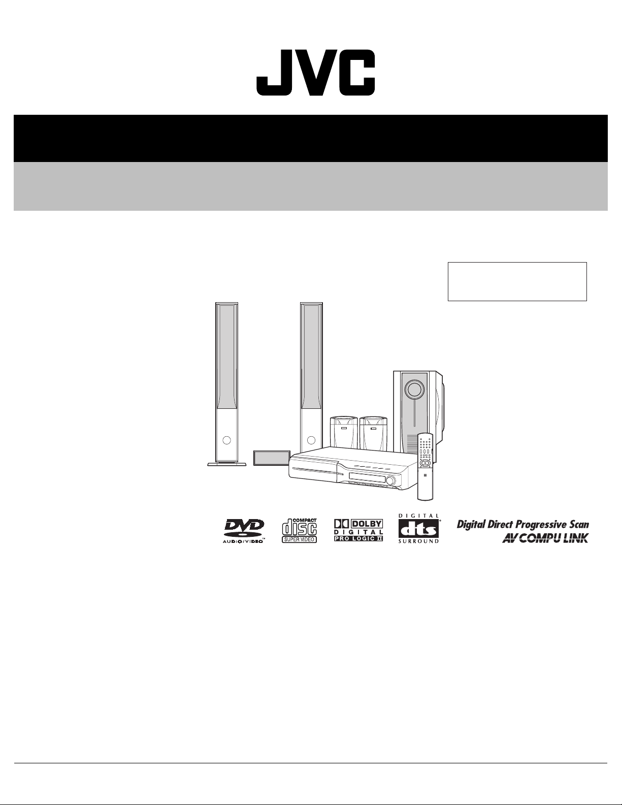
DVD DIGITAL THEATER SYSTEM
MB41520057
TH-C7
Area suffix
J ---------------------------- U.S.A.
(SP-THC7C)
(SP-PWC7)
(SP-THC7F)
(SP-THC5S)
(XV-THC7)
Lead free solder used in the board (material : Sn-Ag-Cu, melting point : 219 Centigrade)
TABLE OF CONTENTS
1 PRECAUTION. . . . . . . . . . . . . . . . . . . . . . . . . . . . . . . . . . . . . . . . . . . . . . . . . . . . . . . . . . . . . . . . . . . . . . . . . 1-4
2 SPECIFIC SERVICE INSTRUCTIONS . . . . . . . . . . . . . . . . . . . . . . . . . . . . . . . . . . . . . . . . . . . . . . . . . . . . . . 1-7
3 DISASSEMBLY . . . . . . . . . . . . . . . . . . . . . . . . . . . . . . . . . . . . . . . . . . . . . . . . . . . . . . . . . . . . . . . . . . . . . . . 1-8
4 ADJUSTMENT . . . . . . . . . . . . . . . . . . . . . . . . . . . . . . . . . . . . . . . . . . . . . . . . . . . . . . . . . . . . . . . . . . . . . . . 1-30
5 TROUBLESHOOTING . . . . . . . . . . . . . . . . . . . . . . . . . . . . . . . . . . . . . . . . . . . . . . . . . . . . . . . . . . . . . . . . . 1-35
COPYRIGHT © 2005 Victor Company of Japan, Limited
No.MB415
2005/7
Page 2
SPECIFICATION
Center unit (XV-THC7)
Audio section Total Harmonic Distortion *1 0.02%
Digital input *2 DIGITAL IN (DBS)
(OPTICAL)
Video section Video System NTSC
Horizontal Resolution 500 lines
Signal-to-Noise Ratio 64 dB
Video output level Composite 1.0 V(p-p)/75 Ω
S-video-Y 1.0 V(p-p)/75 Ω
S-video-C 0.286 V(p-p)/75 Ω
Component-Y 1.0 V(p-p)/75 Ω
Component-PB/PR 0.7 V(p-p)/75 Ω
Video input sensitivity/
Impedance (VCR IN)
Tuner section Tuning Range FM 87.5 MHz to 108.0 MHz
General Power Requirements AC 120 V , 60 Hz
Power Consumption 16 W (at operation)
Dimensions (W × H × D) 400 mm × 85 mm × 399 mm(15-3/4 inches × 3-3/8 inches × 15-3/4 inches)
Mass 4.2 kg (9.3 lbs)
Composite 1.0 V(p-p)/75 Ω
S-video-Y 1.0 V(p-p)/75 Ω
S-video-C 0.286 V(p-p)/75 Ω
AM 530 kHz to 1 710 kHz
- 21 dBm to - 15 dBm
(660 nm ±30 nm)
1.3 W (in standby mode)
*1: This value is measured at System cord CONNECTOR for reference.
*2: Corresponding to Linear PCM, Dolby Digital, and DTS Digital Surround (with sampling frequency -32 kHz, 44.1 kHz, 48 kHz)
Subwoofer (SP-PWC7)
Amplifier section Front/Center/Surround 167 W per channel, RMS at 3 Ω at 1kHz, with 10 % total harmonic distortion.
Subwoofer 167 W, RMS at 3 Ω at 100 Hz, with 10 % total harmonic distortion.
Speaker section Speaker unit 25 cm (9-7/8 inches) Bass-reflex
Power Handling Capacity 170 W
Impedance 3 Ω
Frequency Range 25 Hz to 200 Hz
General Power Requirements AC 120 V , 60 Hz
Power Consumption 160 W (at operation)
0 W (in standby mode)
Dimensions (W × H × D) 264 mm × 481 mm × 459 mm(10-7/16 inches × 18-15/16 inches ×18-1/8 inches)
Mass 16.5 kg (37 lbs)
1-2 (No.MB415)
Page 3
Satellite Speakers (SP-XTHC7)
Front speakers
(SP-THC7F)
Center speaker
(SP-THC7C)
Surround speakers
(SP-THC5S)
Speaker unit Woofer 10 cm (3-15/16 inches) × 4
Power Handling Capacity 170 W
Impedance 3 Ω
Frequency Range 60 Hz to 20 kHz
Dimensions (W × H × D) 270 mm × 1 085 mm × 310 mm(10-11/16 inches × 42-3/4 inches × 12-1/4 inches)
Mass 8.8 kg (19.4 lbs) each
Speaker unit Woofer 10 cm (3-15/16 inches) × 2
Power Handling Capacity 170 W
Impedance 3 Ω
Frequency Range 65 Hz to 20 kHz
Dimensions (W × H × D) 380 mm × 141 mm × 163 mm(15 inches × 4-9/16 inches × 6-7/16 inches)
Mass 3.4 kg (7.5 lbs)
Speaker unit 8.0 cm (3-3/16 inches)
Power Handling Capacity 170 W
Impedance 3 Ω
Frequency Range 80 Hz to 20 kHz
Dimensions (W × H × D) 111.5 mm × 148 mm × 106.5 mm(4-7/16 inches × 5-7/8 inches × 4-1/4 inches)
Mass 0.44 kg (0.97 lbs) each
Tweeter 4 cm (1-5/8 inches)
Bass-reflex, Magnetically Shielded
Tweeter 4 cm (1-5/8 inches)
Bass-reflex, Magnetically Shielded
Bass-reflex
Designs & specifications are subject to change without notice.
(No.MB415)1-3
Page 4
SECTION 1
PRECAUTION
1.1 Safety Precautions
(1) This design of this product contains special hardware and
many circuits and components specially for safety purposes. For continued protection, no changes should be made
to the original design unless authorized in writing by the
manufacturer. Replacement parts must be identical to
those used in the original circuits. Services should be performed by qualified personnel only.
(2) Alterations of the design or circuitry of the product should
not be made. Any design alterations of the product should
not be made. Any design alterations or additions will void
the manufacturers warranty and will further relieve the
manufacture of responsibility for personal injury or property
damage resulting therefrom.
(3) Many electrical and mechanical parts in the products have
special safety-related characteristics. These characteristics are often not evident from visual inspection nor can the
protection afforded by them necessarily be obtained by using replacement components rated for higher voltage, wattage, etc. Replacement parts which have these special
safety characteristics are identified in the Parts List of Service Manual. Electrical components having such features
are identified by shading on the schematics and by ( ) on
the Parts List in the Service Manual. The use of a substitute
replacement which does not have the same safety characteristics as the recommended replacement parts shown in
the Parts List of Service Manual may create shock, fire, or
other hazards.
(4) The leads in the products are routed and dressed with ties,
clamps, tubings, barriers and the like to be separated from
live parts, high temperature parts, moving parts and/or
sharp edges for the prevention of electric shock and fire
hazard. When service is required, the original lead routing
and dress should be observed, and it should be confirmed
that they have been returned to normal, after reassembling.
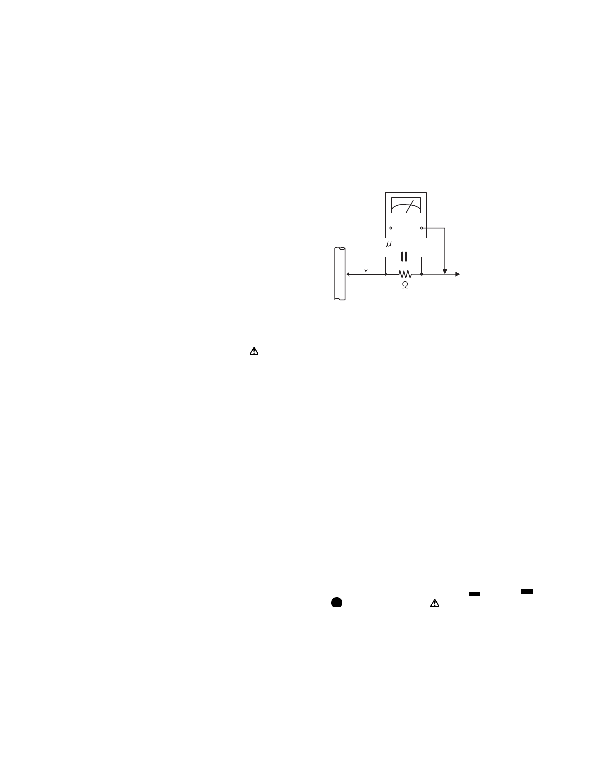
(5) Leakage shock hazard testing
After reassembling the product, always perform an isolation check on the exposed metal parts of the product (antenna terminals, knobs, metal cabinet, screw heads,
headphone jack, control shafts, etc.) to be sure the product
is safe to operate without danger of electrical shock.Do not
use a line isolation transformer during this check.
• Plug the AC line cord directly into the AC outlet. Using a
"Leakage Current Tester", measure the leakage current
from each exposed metal parts of the cabinet, particularly any exposed metal part having a return path to the
chassis, to a known good earth ground. Any leakage current must not exceed 0.5mA AC (r.m.s.).
• Alternate check method
Plug the AC line cord directly into the AC outlet. Use an
AC voltmeter having, 1,000Ω per volt or more sensitivity
in the following manner. Connect a 1,500Ω 10W resistor
paralleled by a 0.15µF AC-type capacitor between an ex-
posed metal part and a known good earth ground.
Measure the AC voltage across the resistor with the AC
voltmeter.
Move the resistor connection to each exposed metal
part, particularly any exposed metal part having a return
path to the chassis, and measure the AC voltage across
the resistor. Now, reverse the plug in the AC outlet and
repeat each measurement. Voltage measured any must
not exceed 0.75 V AC (r.m.s.). This corresponds to 0.5
mA AC (r.m.s.).
AC VOLTMETER
(Having 1000
ohms/volts,
or more sensitivity)
0.15 F AC TYPE
Place this
probe on
1500 10W
Good earth ground
1.2 Warning
(1) This equipment has been designed and manufactured to
meet international safety standards.
(2) It is the legal responsibility of the repairer to ensure that
these safety standards are maintained.
(3) Repairs must be made in accordance with the relevant
safety standards.
(4) It is essential that safety critical components are replaced
by approved parts.
(5) If mains voltage selector is provided, check setting for local
voltage.
1.3 Caution
Burrs formed during molding may be left over on some parts
of the chassis.
Therefore, pay attention to such burrs in the case of preforming repair of this system.
1.4 Critical parts for safety
In regard with component parts appearing on the silk-screen
printed side (parts side) of the PWB diagrams, the parts that are
printed over with black such as the resistor ( ), diode ( )
and ICP ( ) or identified by the " " mark nearby are critical
for safety. When replacing them, be sure to use the parts of the
same type and rating as specified by the manufacturer.
(This regulation dose not Except the J and C version)
each exposed
metal part.
1-4 (No.MB415)
Page 5
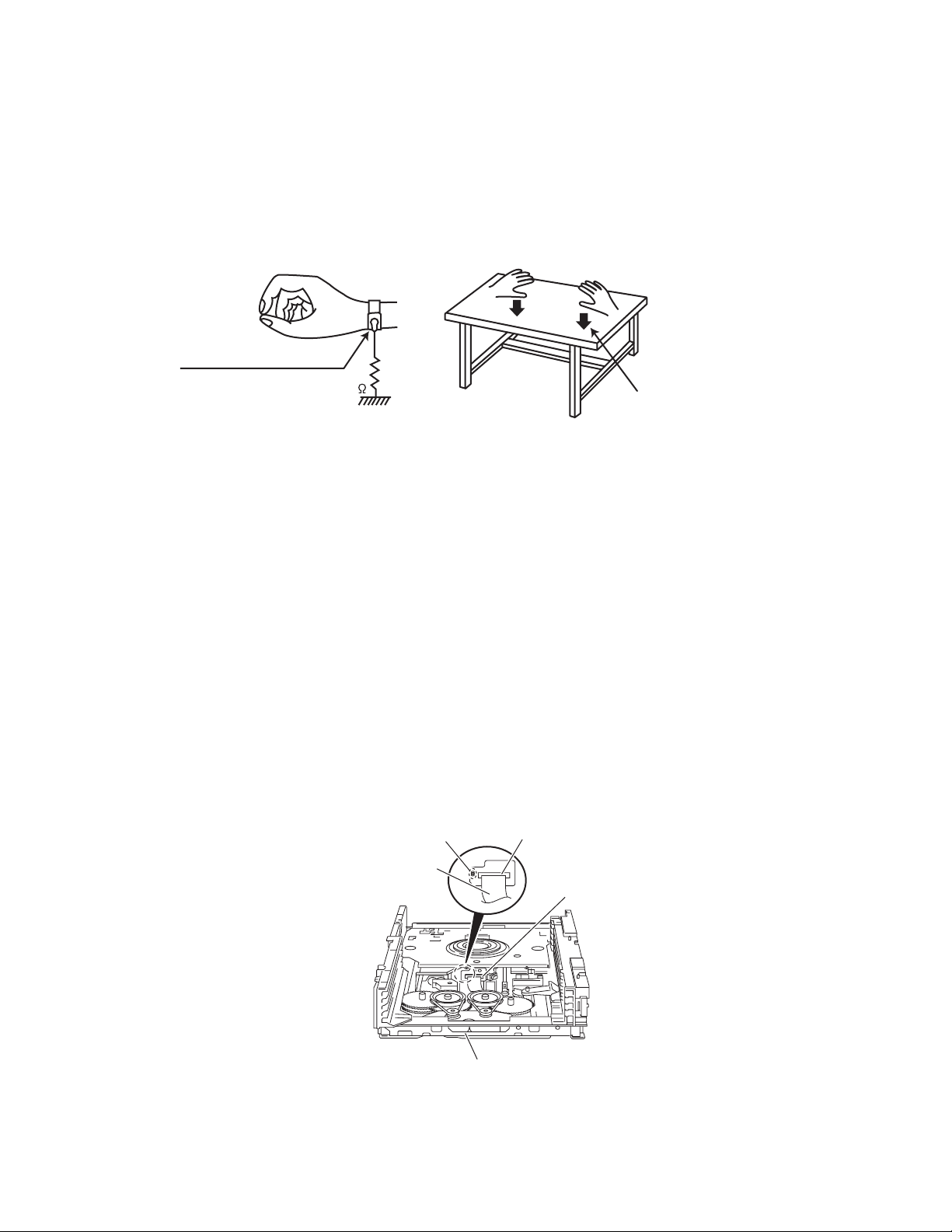
1.5 Preventing static electricity
Electrostatic discharge (ESD), which occurs when static electricity stored in the body, fabric, etc. is discharged, can destroy the laser
diode in the traverse unit (optical pickup). Take care to prevent this when performing repairs.
1.5.1 Grounding to prevent damage by static electricity
Static electricity in the work area can destroy the optical pickup (laser diode) in devices such as laser products.
Be careful to use proper grounding in the area where repairs are being performed.
(1) Ground the workbench
Ground the workbench by laying conductive material (such as a conductive sheet) or an iron plate over it before placing the
traverse unit (optical pickup) on it.
(2) Ground yourself
Use an anti-static wrist strap to release any static electricity built up in your body.
(caption)
Anti-static wrist strap
1M
Conductive material
(conductive sheet) or iron palate
(3) Handling the optical pickup
• In order to maintain quality during transport and before installation, both sides of the laser diode on the replacement optical
pickup are shorted. After replacement, return the shorted parts to their original condition.
(Refer to the text.)
• Do not use a tester to check the condition of the laser diode in the optical pickup. The tester's internal power source can easily
destroy the laser diode.
1.6 Handling the traverse unit (optical pickup)
(1) Do not subject the traverse unit (optical pickup) to strong shocks, as it is a sensitive, complex unit.
(2) Cut off the shorted part of the flexible cable using nippers, etc. after replacing the optical pickup. For specific details, refer to the
replacement procedure in the text. Remove the anti-static pin when replacing the traverse unit. Be careful not to take too long a
time when attaching it to the connector.
(3) Handle the flexible cable carefully as it may break when subjected to strong force.
(4) I t is not possible to adjust the semi-fixed resistor that adjusts the laser power. Do not turn it.
1.7 Attention when traverse unit is decomposed
*Please refer to "Disassembly method" in the text for the pickup unit.
• Apply solder to the short land sections before the flexible wire is disconnected from the connecto on the servo board. (If the flexible
wire is disconnected without applying solder, the pickup may be destroyed by static electricity.)
• In the assembly, be sure to remove solder from the short land sections after connecting the flexible wire.
Short land section
Connector
Card wire
DVD pickup
DVD changer mechanism assembly
(No.MB415)1-5
Page 6
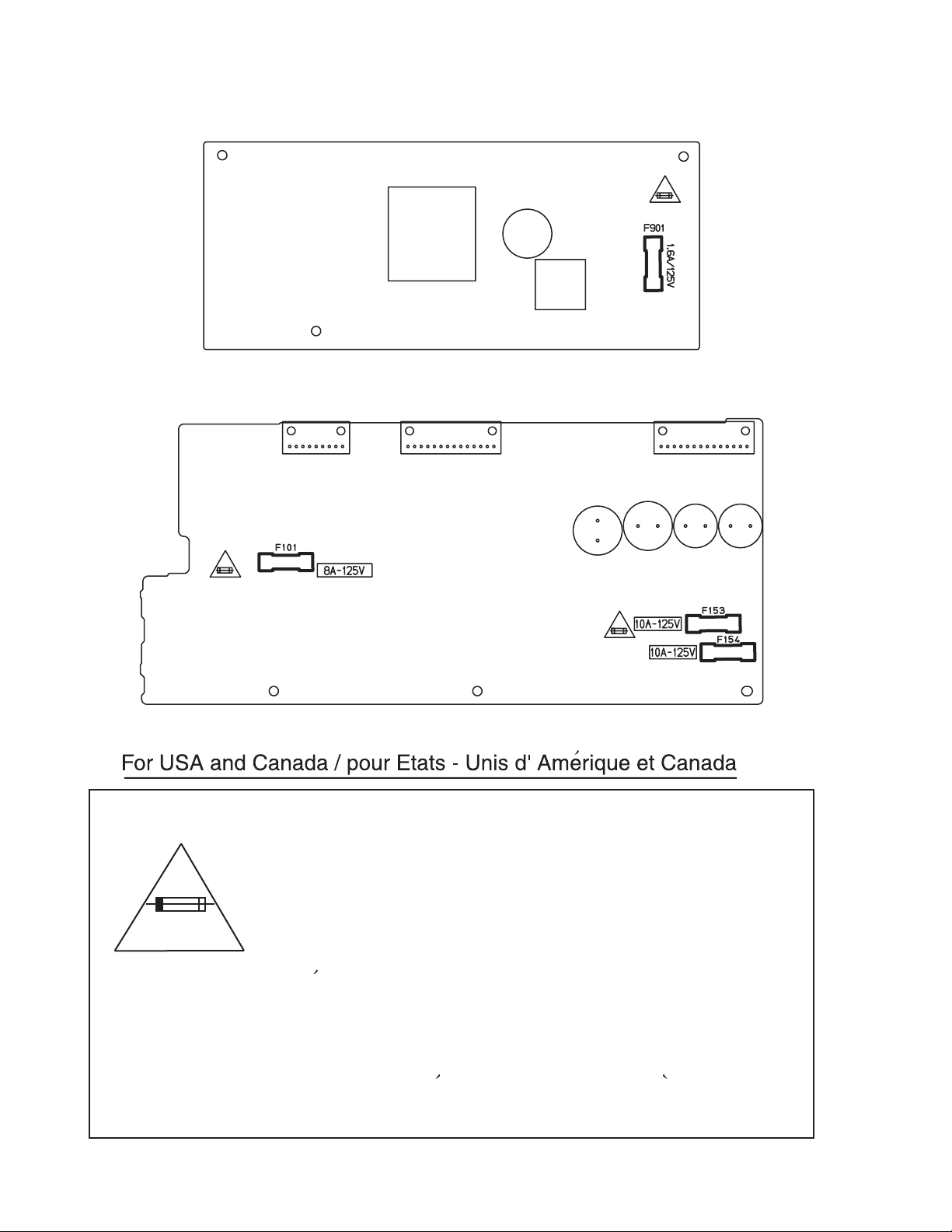
1.8 Importance administering point on the safety
Power supply board
(Center unit)
Mother board
(Subwoofer)
1-6 (No.MB415)
Caution: For continued protection against risk of fire,
replace only with same type 1.6 A/125 V for F901,
8A/125V for F101,10 A/125 V for F153 and F154.
This symbol specifies the type of fast operating fuse.
Precaution: Pour la protection continue contre les
risques d'incendie, remplacer uniquement par le
^
meme type: fusible 1.6 A/125 V pour le F901,
8A/125V pour le F101,10 A/125 V pour le F153 et F154.
Ce symbole specifie le type de fusible a action rapide.
Page 7

SECTION 2
SPECIFIC SERVICE INSTRUCTIONS
This service manual does not describe SPECIFIC SERVICE INSTRUCTIONS.
(No.MB415)1-7
Page 8
SECTION 3
r
DISASSEMBLY
3.1 Main body section
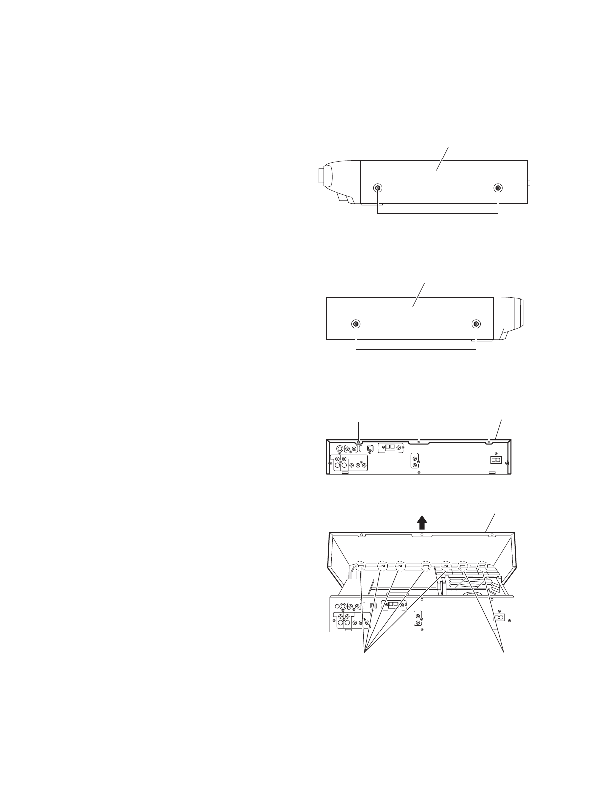
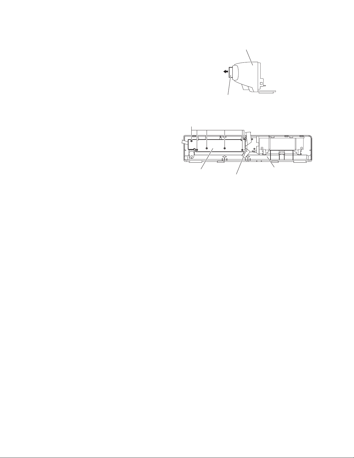
3.1.1 Removing the metal cover
(See Figs. 1 to 4)
(1) From the both sides of the main body, remove the four
screws A attaching the metal cover. (See Figs. 1 and 2.)
(2) From the back side of the main body, remove the three
screws B attaching the metal cover. (See Fig. 3.)
(3) Lift the rear section of the metal cover in the direction of the
arrow while extending the lower sections of the metal cover, release the seven claws a using a longer screwdriver
from the inside as required. (See Fig. 4.)
Note:
Do not damage any parts and boards inside the main body
when releasing the claws a using a longer screwdriver.
Metal cover
A
Fig.1
Metal cover
B
A
Fig.2
Metal cove
Fig.3
Metal cover
Claws aClaws a
1-8 (No.MB415)
Fig.4
Page 9
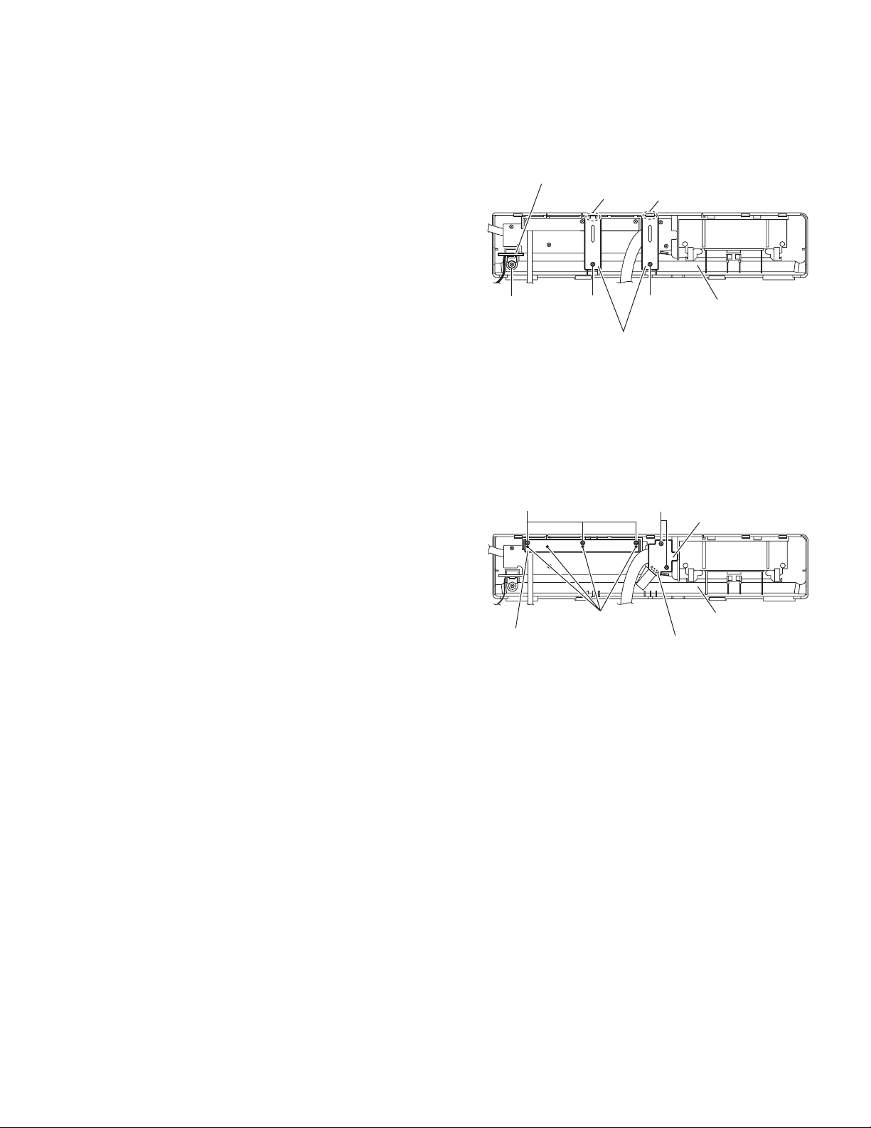
3.1.2 Removing the front panel assembly
(See Figs. 5 and 6)
• Prior to performing the following procedures, remove the metal
cover.
(1) From the top side of the main body, disconnect the parallel
wires from the connectors (CN456
board. (See Fig. 5.)
(2) Disconnect the card wires from the connectors (CN450
) on the main board. (See Fig. 5.)
CN460
(3) Remove the screw C attaching the earth wires to the main
board. (See Fig. 5.)
Reference:
When attaching the screw C, attach the earth wires with
it. (See Fig. 5.)
(4) From the bottom side of the main body, remove the three
screws D attaching the front panel assembly. (See Fig. 6.)
(5) From the both and bottom sides of the main body, remove
the front panel assembly in the direction of the arrow while
releasing the joints b and c. (See Fig. 6.)
, CN457) on the main
,
Front panel assembly
Main board
Card wire
CN457
CN450
CN456
Parallel wires
C
Earth
wires
CN460
Card wire
Front panel assembly
Fig.5
Joint c Joint bJoint b
D
Fig.6
(No.MB415)1-9
Page 10
3.1.3 Removing the DVD changer mechanism assembly
(See Fig. 7)
• Prior to performing the following procedures, remove metal
cover and front panel assembly.
(1) From the top side of the main body, remove the screw E at-
taching the wire protection board to the main board.
(2) Take out the wire protection board, and disconnect the
card wires from the connectors (CN401
main board.
Reference:
When attaching the wire protection board, attach the
wire protection board after connecting the card wires to
the connectors (CN401
(3) Remove the four screws F attaching the DVD changer
mechanism assembly on the bottom chassis.
(4) Take out the DVD changer mechanism assembly in the up-
ward direction.
Reference:
When attaching the DVD changer mechanism assembly, align
the holes of the DVD changer mechanism assembly to the projections d on the bottom chassis.
3.1.4 Removing the rear panel
(See Fig. 8)
• Prior to performing the following procedures, remove the metal
cover.
(1) From the back side of the main body, remove the screw G
and eleven screws H attaching the rear panel.
to CN403) on the main board.
to CN403) on the
F
DVD changer mechanism assembly
Projections d
Wire protection board
F
G
F
E
Fig.7
CN402
Card wires
CN401
Bottom
chassis
CN403
Main
board
H
H
Rear panel
Fig.8
1-10 (No.MB415)
Page 11
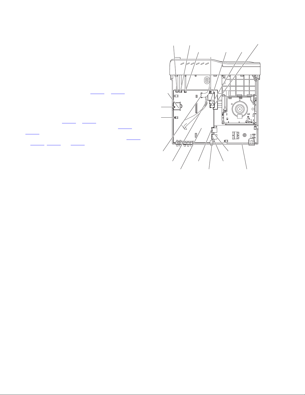
3.1.5 Removing the audio & digital input board
(See Figs. 9 and 10)
• Prior to performing the following procedures, remove the metal
cover.
(1) From the top side of the main body, disconnect the card
wires from the connectors (CN411
board. (See Fig. 9.)
(2) Remove the screw J attaching the earth wires to the main
board. (See Fig. 9.)
Reference:
When attaching the screw J, attach the earth wires with
it. (See Fig. 9.)
(3) From the back side of the main body, remove the screw K
and two screws L attaching the audio & digital input board
to the rear panel. (See Fig. 10.)
(4) Move the audio & digital input board in the direction of the
arrow, and release the claw e of bracket board. (See Fig.
9.)
(5) Take out the audio & digital input board from the main
body.
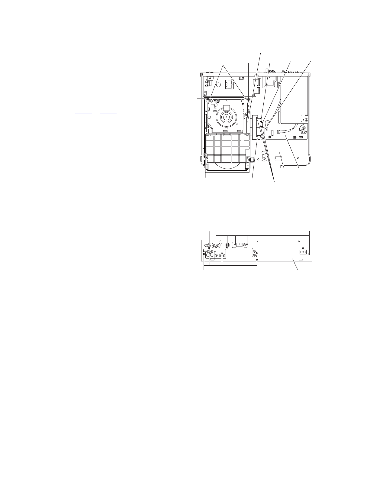
3.1.6 Removing the tuner
(See Figs. 9 and 10)
• Prior to performing the following procedures, remove the metal
cover.
(1) From the top side of the main body, disconnect the card
wire from the connector CN1
(2) From the back side of the main body, remove the two
screws M attaching the tuner to the rear panel. (See Fig.
10.)
(3) Take out the tuner from the main body.
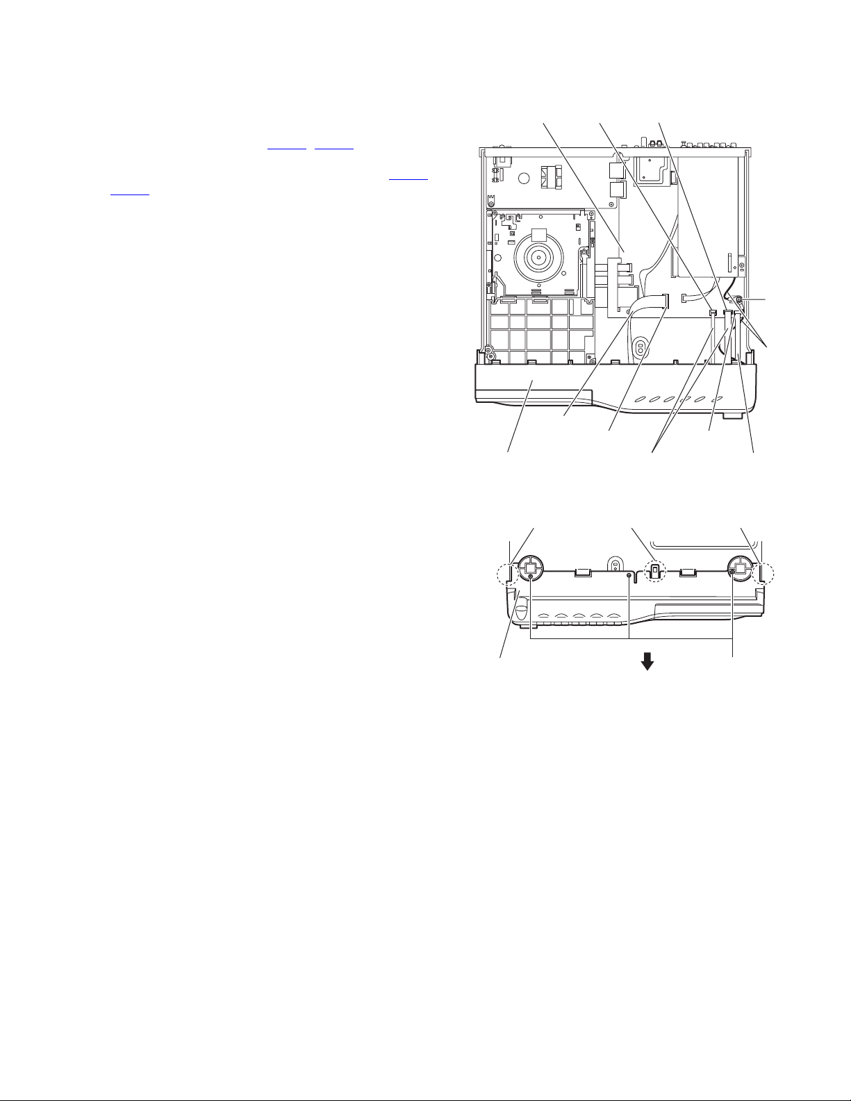
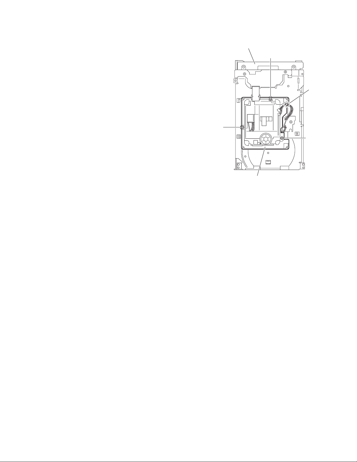
3.1.7 Removing the power supply board
(See Figs. 9 and 10)
• Prior to performing the following procedures, remove the metal
cover.
(1) From the top side of the main body, disconnect the parallel
wires from the connectors (CN404
board. (See Fig. 9.)
(2) Remove the three screws N attaching the power supply
board. (See Fig. 9.)
(3) From the back side of the main body, remove the screw P
attaching the power supply board to the rear panel. (See
Fig. 10.)
(4) Take out the power supply board from the main body.
Reference:
Remove the rear panel as required. (See "3.1.4 Removing the
rear panel")
, CN412) on the main
on the tuner. (See Fig. 9.)
to CN407) on the main
Main board
Card wires
Earth
wire
CN412
CN411
J
Bracket
board
Craw e
CN407
CN406
CN1
Card wire
Audio & digital input board
KP
CN405
Tuner
ML
N
Power supply board
N
CN404
Parallel wires
Fig.9
Rear panel
Fig.10
(No.MB415)1-11
Page 12
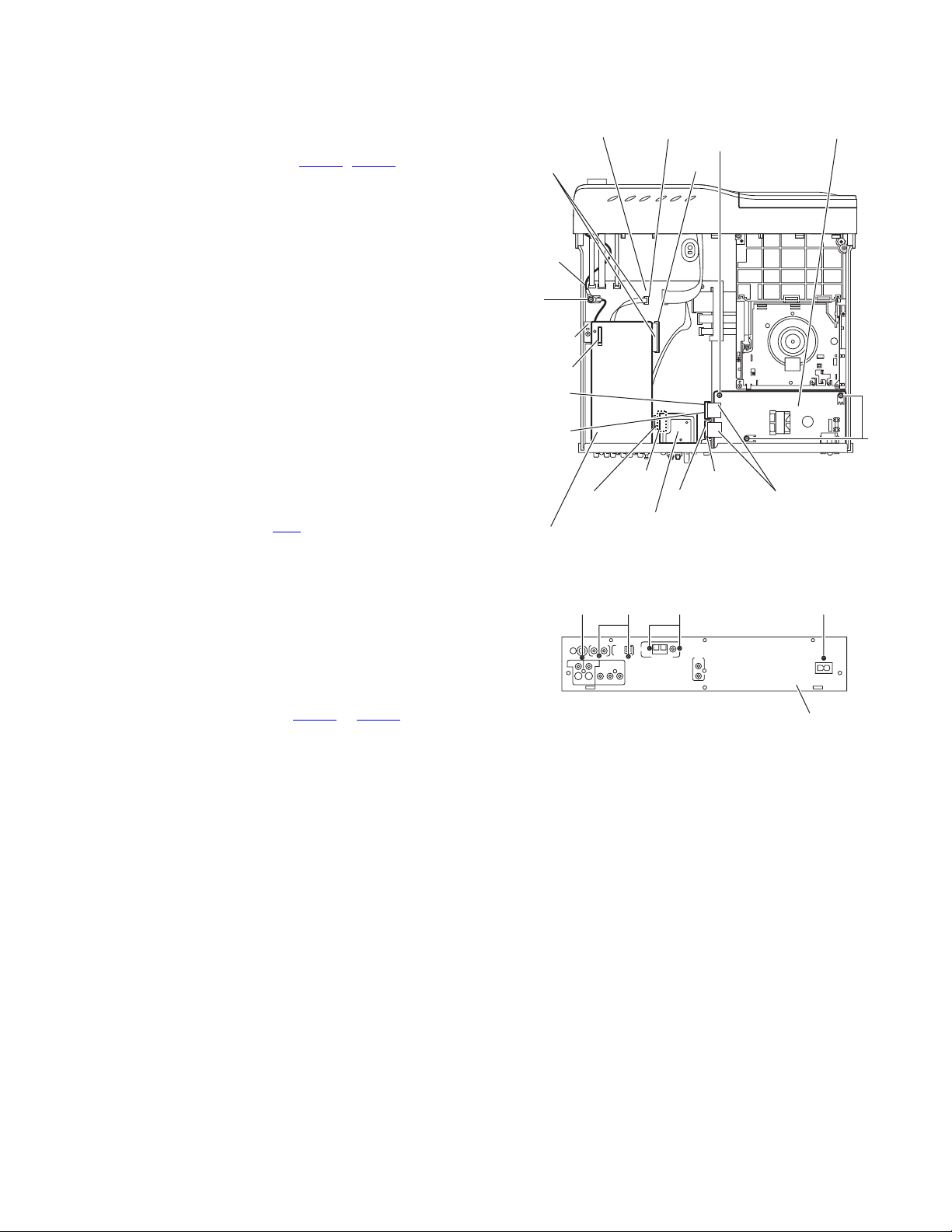
3.1.8 Removing the main board
(See Fig. 11)
• Prior to performing the following procedures, remove the metal
cover, rear panel, audio & digital input board and tuner.
(1) From the top side of the main body, remove the screw Q
attaching the bracket board and take the bracket board.
(2) Remove the screw R and screw R' attaching the main
board on the bottom chassis.
Reference:
When attaching the screw R', attach the wire protection
board with it.
(3) Take out the wire protection board, and disconnect the
card wires from the connectors (CN401
main board.
Reference:
When attaching the wire protection board, attach the
wire protection board after connecting the card wires to
the connectors (CN401
(4) Disconnect the card wires from the connectors (CN450 and
) on the main board.
CN460
(5) Disconnect the parallel wires from the connectors (CN404
to CN407, CN456 and CN457) on the main board.
(6) Take out the main board from the main body.
to CN403) on the main board.
to CN403) on the
CN460
Bracket
board
Q
R
CN450
CN456
CN457
Wire protection board
CN402CN401
R'
CN406
CN403
Main board
CN407
CN404
Fig.11
CN405
Bottom chassis
1-12 (No.MB415)
Page 13
3.2 Front panel assembly section
• Prior to performing the following procedures, remove the front panel assembly from the main body. (See "Removing the front panel
assembly")
3.2.1 Removing the phone jack board
(See Fig. 1)
(1) From the inside of the front panel assembly, remove the
screw A attaching the phone jack board.
(2) Take out the phone jack board from the front panel assem-
bly.
3.2.2 Removing the bracket board
(See Fig. 1)
(1) From the inside of the front panel assembly, remove the
two screws B attaching the bracket board.
Reference:
When attaching the connect board, align the projections
of the bracket board to the slots a and b of the front panel
assembly.
(2) Take out the bracket board from the front panel assembly.
3.2.3 Removing the operation board
(See Fig. 2)
• Prior to performing the following procedures, remove the
bracket board.
(1) From the inside of the front panel assembly, remove the
three screws C attaching the operation board.
Reference:
When attaching the operation board, align the projections c of the front panel assembly to the holes of the operation board.
(2) Take out the operation board.
3.2.4 Removing the power key board
(See Fig. 2)
• Prior to performing the following procedures, remove the
bracket board.
(1) From the inside of the front panel assembly, remove the
two screws D attaching the power key board.
(2) Take out the power key board and remove the solder from
the soldered point d to remove the parallel wire.
Phone jack board
A
Operation board
Slot b
Bracket board
Projections c
Slot a
Front panel assembly
BB
Fig.1
DC
Power key board
Front panel assembly
Solder section d
Fig.2
(No.MB415)1-13
Page 14
3.2.5 Removing the front board
(See Figs. 3 and 4)
• Prior to performing the following procedures, remove the
phone jack board, bracket board and operation board.
(1) From the front side of the front panel assembly, pull out the
volume knob in the direction of the arrow. (See Fig. 3.)
(2) From the inside of the front panel assembly, remove the six
screws E attaching the front board. (See Fig. 4.)
(3) Take out the front board and remove the solder from the
soldered point e to remove the parallel wire. (See Fig. 4.)
Front panel assembly
Volume knob
Fig.3
E
Front board
Front panel assembly
Solder section e
Fig.4
1-14 (No.MB415)
Page 15
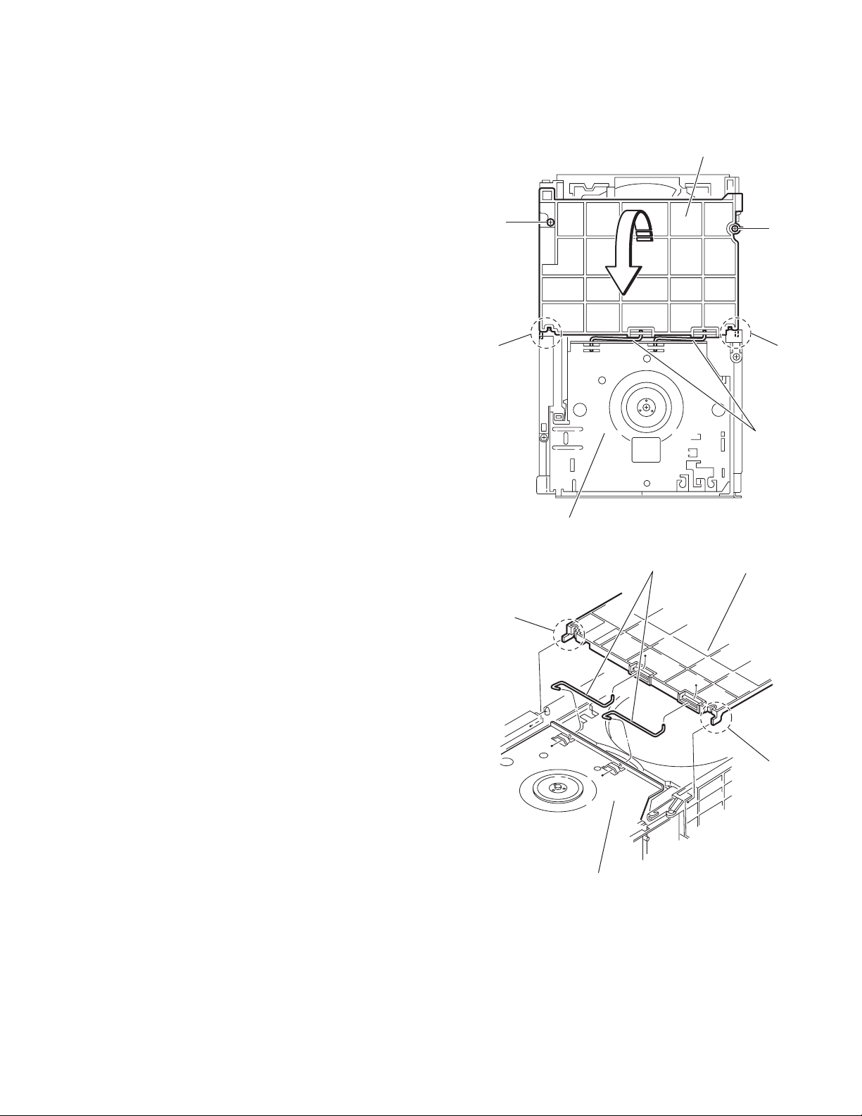
3.3 DVD changer mechanism assembly section
Remove the DVD changer mechanism assembly from the main body. (See "Removing the DVD changer mechanism assembly".)
3.3.1 Removing the tray assemblies
(See Figs.1 to 5)
(1) From the top side of the main body, remove the two screws
A from the top cover and release the two joints a on the
both sides of the DVD changer mechanism assembly. (See
Figs.1 and 2.)
(2) Remove the two rods from the top cover and remove the
top cover from the lifter assembly. (See Figs.1 and 2.)
(3) Remove the open det. lever on the left side of the DVD
changer mechanism assembly. (See Fig.3.)
(4) From the right side of the DVD changer mechanism as-
sembly, draw out the tray assemblies toward the front while
pushing the part b of the side (R) assembly. (See Figs.4
and 5.)
Note:
The tray can be locked if all tray assemblies are attached.
(5) From the topside of the DVD changer mechanism assem-
bly, move the stopper tabs c in the direction of the arrow
and release them. Pull out the tray assemblies from the
DVD changer mechanism assembly. (See Fig. 5.)
Note:
Remove the tray assembly from top tray 5 in order.
Reference:
When reattaching the tray assembly, or when removing the
disc remaining inside, refer to another section "3.3.15 Taking
out the disc in the play mode".
A
a
Lifter assembly
Fig.1
Rods
Top cover
A
a
Rods
Top cover
a
a
Lifter assembly
Fig.2
(No.MB415)1-15
Page 16
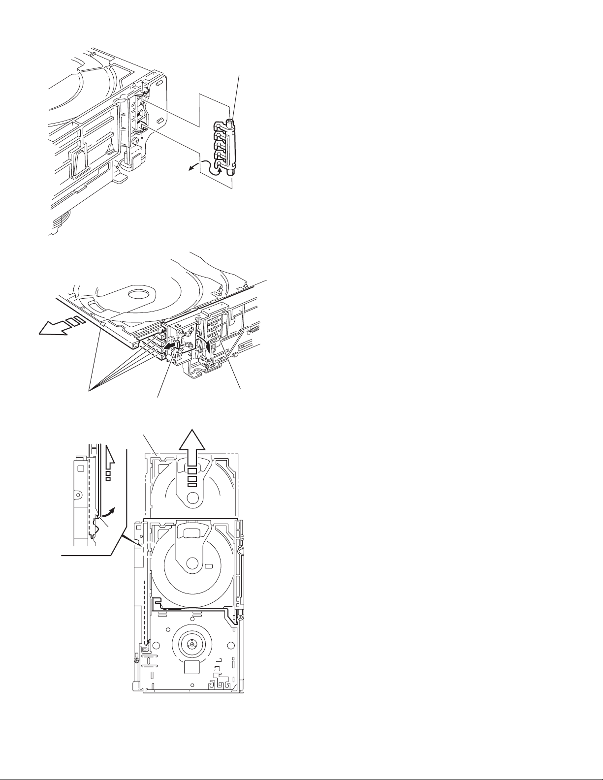
Fig.3
r
Open det. leve
Tray assemblies
c
b
Side(R) assembly
Fig.4
Tray assembly
1-16 (No.MB415)
Fig.5
Page 17
3.3.2 Removing the DVD servo board
(See Figs.6 to 8)
Caution:
Solder the short land sections d on the DVD pickup before disconnecting the card wire extending from the DVD pickup. If
you do not follow this instruction, the DVD pickup may be damaged.
(1) From the topside of the DVD changer mechanism assem-
bly, solder the short land sections d on the DVD pick up.
(See Fig.6.)
(2) From the bottom side of the DVD changer mechanism as-
sembly, disconnect the card wire from the connectors
(CN201
Reference:
(3) Disconnect the wires from the connectors (CN452
on the DVD servo board. (See Fig.7.)
(4) Remove the two screws B attaching the DVD servo board.
(See Fig.7.)
(5) From the reverse side of the DVD servo board, release the
lock of the connector CN101
and disconnect the card wire. (See Fig.8.)
Caution:
Unsolder the solders from the short land sections d after reassembling. (See Fig.6.)
3.3.3 Removing the switch board
(1) From the bottom side of the DVD changer mechanism as-
sembly, remove the screw C attaching the switch board on
the DVD changer mechanism assembly.
(2) Disconnect the wires from the connectors (CN452
on the DVD servo board.
(3) Release the wires from the section f and remove the switch
board.
(4) Release the wires from the sections g and remove the
switch board.
Reference:
When reassembling, pass the wires through the sections (f, g)
as before.
, CN451) on the DVD servo board. (See Fig.7.)
When connecting the card wire to the connector CN451
pass it through the sections e on the DVD traverse
mechanism assembly. (See Fig.7.)
, CN453)
in the direction of the arrow
(See Fig.7)
, CN453)
d
,
DVD changer mechanism assembly
Fig.6
DVD changer mechanism assembly
e
CN451
DVD pickup
CN453
f
g
Switch board
B
C
CN201
DVD servo board
DVD traverse mechanism assembly
DVD servo board
B
Fig.7
CN452
CN101
Fig.8
Lock
(No.MB415)1-17
Page 18
3.3.4 Removing the motor board
(See Figs.9 and 10)
(1) From the top side of the DVD changer mechanism assem-
bly, remove the two belts from the motor pulleys. (See
Fig.9.)
Note:
Take care not to attach grease on the belt.
(2) Remove the two screws D attaching the motors to the load-
er assembly. (See Fig.9.)
(3) From the bottom side of the DVD changer mechanism as-
sembly, remove the two screws E. (See Fig.10.)
(4) Disconnect the connector CN2
tray switch board and remove the motor board. (See
Fig.10.)
(5) Disconnect the card wire from the connector CN1
forward side of the motor board. (See Fig.10.)
Note:
When connecting the card wire, let the card wire through the
slots h of the motor board. (See Fig.10.)
Reference:
You need not to remove the tray assemblies, and in such case,
move it.
3.3.5 Removing the motor
(See Fig. 10)
• Remove the motor board.
(1) From the reverse side of the motor board, unsolder the four
soldered sections i on the motor board.
(2) From the forward side of the motor board, remove the mo-
tors.
on the motor board from the
on the
D
Belt
Motor Motor
Motor pulleys
Belt
D
Loader assembly
Fig.9
Motors
Motor board
i
Tray switch
board
E
CN2
CN1
h
DVD changer mechanism assembly
Fig.10
Motors
Motor board
E
1-18 (No.MB415)
Page 19
3.3.6 Removing the DVD traverse mechanism assembly
(See Fig.11)
• Remove the tray assemblies and DVD servo board.
(1) From the bottom side of the DVD changer mechanism as-
sembly, remove the three screws F attaching the DVD
traverse mechanism assembly.
(2) Remove the wires from the section j.
(3) Take out the DVD traverse mechanism assembly from the
DVD changer mechanism assembly.
DVD changer mechanism assembly
F
j
F
F
DVD traverse mechanism assembly
Fig.11
(No.MB415)1-19
Page 20
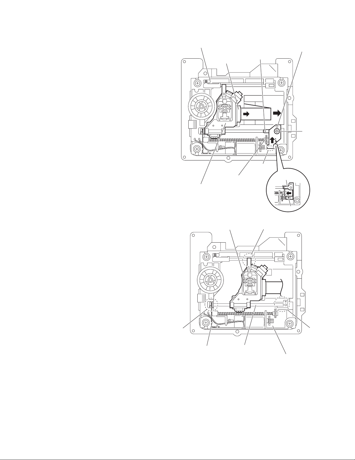
3.3.7 Removing the DVD pickup
(See Figs.12 to 14)
• Remove the tray assemblies, DVD servo board and DVD
traverse mechanism assembly.
(1) From the top side of the DVD traverse mechanism assem-
bly, release the lock of the connector on the DVD pickup
and disconnect the card wire in the direction of the arrow.
(See Fig.12.)
(2) Turn the screw shaft gear in the direction of the arrow 1 to
move the DVD pickup in the direction of the arrow 2. (See
Fig.12.)
(3) Remove the screw G attaching the feed bracket and re-
move the feed bracket from the sections k. (See Fig.12.)
(4) Release the claw m of the thrust spring in the direction of
the arrow and remove the thrust spring. (See Fig.12.)
(5) Remove the guide shaft from the sections (n, p) on the
C.TM chassis. (See Fig.13.)
(6) Remove the section q of the DVD pickup. (See Fig.13.)
(7) Remove the two screws H attaching the rack arm spring
and rack arm. (See Fig.14.)
(8) Pull the guide shaft from the DVD pickup in the direction of
the arrow. (See Fig.14.)
3.3.8 Attaching the DVD pickup
(See Figs.12 to 14)
(1) Attach the guide shaft to the DVD pickup and attach the
rack arm spring and rack arm with the screws H. (See
Fig.14.)
(2) Attach the section q of the DVD pickup to the C.TM chassis
first and attach the guide shaft to the sections (n, p). (See
Fig.13.)
Reference:
When attaching the guide shaft to the section p, attach it
under the rod spring. (See Fig.13.)
(3) Attach the thrust spring and feed bracket with the screw G.
(See Fig.12.)
(4) Turn the screw shaft gear in the direction of the arrow 1 to
move the DVD pickup in the direction of the arrow 2. (See
Fig.15.)
(5) Connect the card wire to the connector on the DVD pickup.
(See Fig.15.)
DVD traverse mechanism assembly
Thrust spring
Connector
Screw shaft gear
DVD pickup
Fig.12
DVD pickup
1
k
Thrust spring
q
Feed bracket
2
G
m
1-20 (No.MB415)
p
Rod spring
n
Guide shaft
C.TM chassis
Fig.13
Page 21
Guide shaft
DVD pickup
Rack arm
H
Rack arm spring
Fig.14
Connector
DVD pickup
222
Screw shaft gear
Fig.15
1
(No.MB415)1-21
Page 22
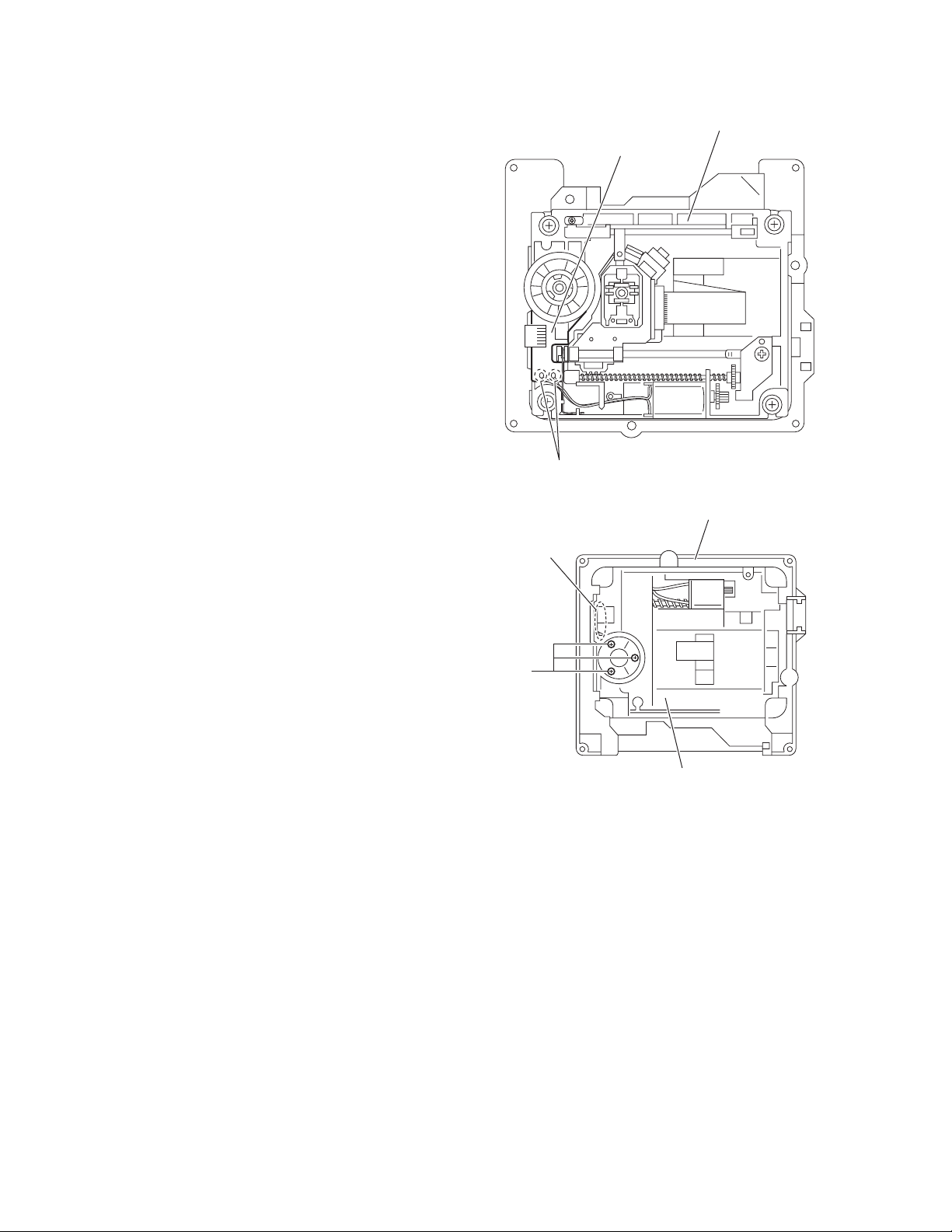
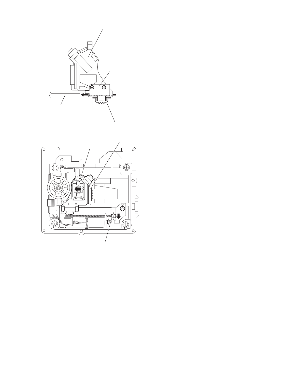
3.3.9 Removing the spindle motor board
(See Figs.16 and 17)
• Remove the tray assemblies, DVD servo board and DVD
traverse mechanism assembly.
(1) From the top side of the DVD traverse mechanism assem-
bly, remove the wires from the soldered sections r on the
spindle motor board. (See Fig.16.)
(2) From the bottom side of the DVD traverse mechanism as-
sembly, remove the three screws J attaching the spindle
motor board. (See Fig.17.)
Reference:
When attaching the spindle motor board, let the card wire
through the hole s on the C.TM chassis. (See Fig.17.)
DVD traverse mechanism assembly
Spindle motor board
r
Fig.16
DVD traverse mechanism assembly
s
J
C.TM chassis
Fig.17
1-22 (No.MB415)
Page 23

3.3.10 Removing the feed motor
(See Figs.18 and 19)
• Remove the tray assemblies and DVD traverse mechanism
assembly.
(1) From the top side of the DVD traverse mechanism assem-
bly, remove the screw K attaching the feed bracket and remove the feed bracket from the sections t. (See Fig.18.)
(2) Release the claw u of the thrust spring in the direction of
the arrow and remove the thrust spring. (See Fig.18.)
(3) Remove the screw shaft from the section v and remove it
in the direction of the arrow. (See Fig.19.)
(4) Remove the middle gear. (See Fig.19.)
(5) Remove the screw L attaching the feed motor to the C.TM
chassis. (See Fig.19.)
(6) Remove the wires from the soldered sections w on the
spindle motor board. (See Fig.19.)
(7) Take out the feed motor from the motor base.
Reference:
After attaching the feed motor, pass the wires through the sections x on the C.TM chassis as before. (See Fig.19.)
Feed bracket
Thrust spring
K
t
Thrust spring
Spindle motor board
w
x
Fig.18
Middle gear
v
Screw shaft
u
C.TM chassis
Fig.19
L
(No.MB415)1-23
Page 24

3.3.11 Removing the side (L) and tray switch board
(See Figs.20 to 22)
• Remove the tray assemblies.
(1) From the topside of the DVD changer mechanism assem-
bly, remove the two screws M attaching the side (L). (See
Fig.20.)
(2) From the left side of the DVD changer mechanism assem-
bly, disconnect the connector CN3
from the motor board and detach the side (L) in an upward
direction. (See Fig.21.)
(3) Remove the screw N attaching the tray switch board to the
side (L). (See Fig.22.)
(4) Release the joint tab y of the side (L) in the direction of the
arrow 1 and release the joint tab z while removing the tray
switch board in the direction of the arrow 2. (See Fig.22.)
on the tray switch board
SIde(L)
M
M
DVD changer mechanism assembly
Fig.20
M
Side(L)
M
CN3
Tray switch board
Motor board
Side(L)
Fig.21
y
1
1-24 (No.MB415)
2
z
Tray switch board
N
Fig.22
Page 25

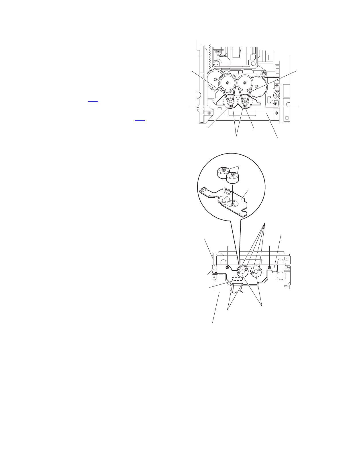
3.3.12 Removing the side (R) assembly
(See Fig.23 to 27)
• Remove the tray assemblies and DVD servo board.
(1) From the inside of the side (R) assembly, release the two
tabs aa of the gear cover and remove the gear cover outward. (See Figs.23 and 24.)
(2) From the right side of the DVD changer mechanism as-
sembly, remove the elevator spring attached to the hook
ab of the loader assembly. (See Figs.24 and 25.)
(3) From the top side of the DVD changer mechanism assem-
bly, turn the gear 1 clockwise to move the elevator cam
rearward. (See Fig.25.)
(4) Move the two slots ac and joint ad of the elevator cam and
remove the elevator cam outward. (See Fig.25.)
(5) Remove the three screws P and detaches the side (R) as-
sembly upward. (See Figs.26 and 27.)
Note:
When reattaching the side (R) assembly, make sure to fit the
shaft (part ae) into the slot of the select lever. (See Fig.26.)
Side(R) assembly
aa
P
Elevator spring
ac
Fig.25
P
ae
ab
Elevator cam
acad
Select lever
Side(R) assembly
Gear cover
Loader assembly
P
Fig.23
Elevator spring
Gear 1
Side(R) assembly
Fig.26
P
ab
P
Fig.24
Side(R) assembly
Fig.27
(No.MB415)1-25
Page 26

3.3.13 Removing the lifter assembly
(See Figs.28 to 32)
• Remove the tray assemblies, DVD servo board, side (L) and
side (R) assembly.
(1) (1) From the top side of the DVD changer mechanism as-
sembly, turn the gear 1 clockwise to move the lifter assembly upward. (See Figs.28 and 29.)
(2) Turn the gear 2 clockwise to move the hook toward the
front until it stops. (See Figs.28 and 29.)
(3) Move the hook stopper in the direction of the arrow 2 while
pushing the tab af of the hook stopper to unlock it in the direction of the arrow 1 and release four joints ag to detach
from the rack holder. (See Fig.30.)
(4) Release the rod (L) from part ah. (See Fig.30.)
(5) Turn the gear 1 clockwise again to move the lifter assembly
upward. (See Fig.31.)
(6) Remove the lifter assembly from the DVD changer mecha-
nism assembly upward at the positions ai where the four
pins on the both sides of the lifter assembly fit to the notch-
es of the loader assembly. (See Fig.31.)
(7) Move the lifter assembly in the direction of the arrow and
release it from the hook. (See Fig.32.)
Hook stopper
Gear 2
Gear 1
ag
Rack holder
af
Hook
ag
1
ag
Hook stopper
Fig.30
Lifter assembly
ag
2
Rod(L)
ai
ah
ai
Hook
Gear 2
Lifter assembly
Fig.28
Gear 1
Lifter assembly
Gear 1
ai
Loader assembly
Fig.31
Lifter assembly
ai
Hook stopper
1-26 (No.MB415)
Hook
Fig.32
Hook
Fig.29
Page 27

3.3.14 Removing the sensor board and SV resistor
(See Fig.33)
• Remove the tray assemblies, side (L), side (R) assembly and
lifter assembly.
(1) Remove the solders from the soldered sections aj on the
sensor board and remove the wires.
(2) Remove the two screws Q and take out the sensor board
with the SV resistor.
Reference:
• Remove the soldered section ap on the sensor board as required.
• When reassembling, pass the wires through the slot ak of
the sensor board as before.
Note:
When reattaching the SV. resister, fit the projection am on the
bottom of the SV. resister into slot an of the sensor slider.
Sensor board
Q
ap
Q
ak
aj
SV resistor
am
an
SV resistor
Slider
Fig.33
(No.MB415)1-27
Page 28

3.3.15 Taking out the disc in the play mode
(See Fig.34 to 37)
Reference:
Refer to "3.3.1 Removing the tray assemblies".
(1) From the top side of the DVD changer mechanism assem-
bly, remove the top cover.
(2) Unlock the tray assemblies and draw out the tray assem-
blies toward the front.
(3) From the top side of the DVD changer mechanism assem-
bly, turn the gear 1 clockwise to move the lifter assembly
upward. (See Fig.34.)
(4) Turn the gear 2 clockwise to move the sub tray remaining
inside the lifter assembly toward the front, then pull out.
(See Fig.34.)
(5) Take out the disc on the sub tray. (See Fig.35.)
(6) After clearing away the disc, insert the sub tray into the
main tray. (See Fig.36.)
Note:
When reattaching the sub tray, move the tray stopper on
the bottom of the main tray in the direction of the arrow
to lock the sub tray certainly. (See Figs.36 and 37.)
(7) Push the tray assembly toward the DVD changer mecha-
nism assembly and reattach.
Tray assembly
Gear 2
Gear 1
Sub tray
Fig.34
Tray assembly
Fig.35
Disc
Sub tray
1-28 (No.MB415)
Page 29

Tray stopper
r
Main tray
Sub tray
Fig.36
Tray stoppe
Fig.37
(No.MB415)1-29
Page 30

SECTION 4
ADJUSTMENT
4.1 Special mode
4.1.1 Outline
The contents in the special mode of operation, and the definition of a key (remote controller or main unit)
4.1.2 Special mode
1.DVD TEST MODE
It goes into the TEST mode of DVD.
DVD TEST mode is canceled by except DVD source, and POWER OFF.
It is referring to the "4.2 DVD test mode" for details.
Insert the power cord in an outlet while
pressing the
on the main unit simultaneously.
2.DVD NORMAL INITIALIZE
Initialize DVD backend memory.
<RDS> segment of FL will light up if successful.
It is referring to the "4.2 DVD test mode" for details.
"POWER"
A main unit entered in the
DVD TEST MODE.
and "PLAY" keys
Press the "PAUSE" key on the remote
controller during the DVD test mode.
DVD initialization is completed
3.DVD FULL INITIALIZE
It is referring to the "4.2 DVD test mode" for details.
Press the 1.5 second "F.SKIP" key on the remote
controller during the DVD test mode.
DVD initialization is completed
4.DVD REGION CHECK
FL display in DVD TEST MODE.
It is referring to the "4.2 DVD test mode" for details.
Press the "MENU" key on the remote
controller during the DVD test mode.
A region No. display
1-30 (No.MB415)
Page 31

5.FORCED NTSC MODE
It is made compulsive NTSC mode.
From this, with regards to the input of NTSEL_SW, there is nothing only
at the time of 1st power on, and it performs NTSC starting.
(Command specification is performed to a module.)
A mode clearance is performed by power off.
VIDEO FORMAT change is prohibited during Forced NTSC mode.
Insert the power cord in an outlet while
"
pressing the "POWER
and "PAUSE" keys
on the main unit simultaneously.
A main unit entered in the
NTSC mode compulsively.
6.TRAY LOCK
A loader mechanism's tray lock is carried out. In the tray lock function ON state,
EJECT processing is not performed to the EJECT key.
And , a LOCK display is performed at this time.
When it turns off a tray lock function, STOP and EJECT KEY are pushed simultaneously again.
Back up ON/OFF of a tray lock.
Press the "STOP" and "OPEN/CLOSE1" keys
on the remote controller at standby.
A tray lock is completed.
4.1.3 Upgrading of firmware (DVD UPGRADE)
The latest firmware for upgrading is updated in "Optical disc CSG" page in JS-net. At the time of service, compare the version of the
product and the latest version, and upgrade the old version into the latest version.
(1) Press "STANDBY/ON" key of the main body to turn it on.
(2) Push "OPEN/CLOSE" key of the main body, and insert the upgrade disc in the tray.
(3) When reading the data of the disc, the OSD screen is displayed "VERSION UP DISC", "PROGRAM & DESTINATION MODE"
and "READING..".
(4) When the screen changes from "READING.." to "WRITING..", upgrading starts.
(5) After writing the data of the disc, the screen is displayed "OPEN".
(6) Take out the disc, and press "STANDBY/ON" key of the main body.
(7) When the stand-by indicator is lighted, upgrading is completed.
(8) Set the main body at test mode, and confirm the version of the firmware. (Refer to "4.2 Method of displaying version firmware".)
4.1.4 Upgrading of system microcomputer (ROM CORRECTION)
(1) Press "STANDBY/ON" key of the main body to turn it on.
(2) Push "OPEN/CLOSE" key of the main body, and insert the upgrade disc in the tray.
(3) When reading the data of the disc, the OSD screen is displayed "VERSION UP DISC", "SYSCON UPG MODE" and "READ-
ING..".
(4) When the screen changes from "READING.." to "WRITING..", system data is written.
(5) After writing the data of the disc, the FL display of the main body is displayed "COMPLETE".
(6) Take out the disc, and press "STANDBY/ON" key of the main body.
(7) When the stand-by indicator is lighted, upgrading is completed.
(8) Set the main body at test mode, and confirm the version of the system microcomputer. (Refer to "4.2 Method of displaying ver-
sion firmware".)
(No.MB415)1-31
Page 32

4.2 DVD TEST MODE
Insert the power cord in an outlet while
pressing the "POWER
on the main unit simultaneously.
"
and "PLAY" keys
FL indication
TEST bb#
It is made POWER ON in test mode, and VERSION is displayed on FL.
TEST bb#
Press the "PAUSE" key on the main unit.
FL indication
TEST bb#
The initialization state (The 11th figure)
"3" : FULL initialization end
"0" : NORMAL initialization end
"Blank" : Initialization un-ending
The study state (The 10th figure)
"3" : DVD Study un-completing, CD Study un-completing
"2" : DVD Study completing, CD Study un-completing
"1" : DVD Study un-completing, CD Study completing
"0" : DVD Study completing, CD Study completing
Region code display
The study state and an initialization state from a back end are
displayed on the 10th and 11th figure of FL display.
Destination VERSION id displayed.
The display to the VERSION code is as follows.
JC / 1U / D / E / 2U / 3U / UB / UT / 4U / UY / EE / UF
NORMAL initialization
segment of FL is RDS on at the time of the completion of
initialization.
Press the "F.SKIP" key on the main unit
or remote controller for a long time.
FL indication
TEST bb#
Press the "MENU" key on the remote controller.
FL indication
(For Example) " 1234 "
Display the checksum of a device key on FL. (4byte)
Press the "MENU" key on the remote controller.
Display the version of a micom on FL.
FL indication
eaa cccc
d bb
aa : SYS, bb : MECHA, cccc : BE
d : MECHACON ROM collection's version
One digit out of two digits is indicated.
e : SYSCON ROM collection's version
One digit out of two digits is indicated.
Press the "MENU" key on the remote controller.
FL indication
ALL FL light UP
Switch on the all-points light of FL and LED.
FULL initialization
segment of FL is RDS on at the time of the completion of
initialization.
1-32 (No.MB415)
1
Page 33

1
Press the "MENU" key on the remote controller.
Enter to CHECK MODE
FL indication
CHECK
Press the "1" key on the remote controller.
Starting of DISC & normal play
(Play from the started position)
Press the "2" key on the remote controller.
Existence of WOBBLE
0 : WOBBLE_NO_CHECK (Un-checking.)
1 : WOBBLE_PRESS_MEDIA (Press)
2 : WOBBLE_MINUS_MEDIA (DVD-R/-RW Media)
3 : WOBBLE_PLUS_MEDIA (DVD+R/+RW Media)
Press the "3" key on the remote controller.
With no assignment
Press the "4" key on the remote controller.
CD_LD lighting & laser current display
Press the "5" key on the remote controller.
DVD_LD lighting & laser current display
FL indication
CHECK
FL indication
FL indication
CHECK
FL indication
FL indication
2 3
Press the "6" key on the remote controller.
FL indication
DVD_SLx1 JITTA measurement mode
Press the "7" key on the remote controller.
FL indication
The contents of a backup memory display (BWD)
Press the "8" key on the remote controller.
FL indication
The contents of a backup memory display (FWD)
Press the "9" key on the remote controller.
FL indication
Temperature sensor value (AD value) display
Press the "10" key on the remote controller.
FL indication
DVD-DL (Parallel, opposite), DVD-SL
Search & JITTA measurement to a predetermined position
(No.MB415)1-33
Page 34

2 3
Press the "0" key on the remote controller.
MONITOR output change
1 : SRV_MONI_CIRC
2 : SRV_MONI_SERVO
3-5 : SRV_MONI_ANALOG
6-7 : SRV_MONI_DRC
8-11 : SRV_MONI_SERVO_JIG
12 : SRV_MONI_DEFAULT
Press the "+10" key on the remote controller.
Initialization of the contents of a backup memory
Press the "STOP" key on the main unit or
remote controller.
Disc stop, LD-OFF
Press the "OPEN/CLOSE" key on the main
unit or remote controller.
Tray open/close
Press the "PLAY" key on the main unit or
remote controller.
Play disc
FL indication
FL indication
FL indication
CHECK
FL indication
CHECK
FL indication
Press the "MENU" key on the remote controller.
FL indication
TEST bb#
Press the "STANDBY" key on the main unit
or remote controller.
Cancellation of the
"DVD TEST MODE"
1-34 (No.MB415)
Page 35

SECTION 5
TROUBLESHOOTING
This service manual does not describe TROUBLESHOOTING.
(No.MB415)1-35
Page 36

Victor Company of Japan, Limited
AV & MULTIMEDIA COMPANY AUDIO/VIDEO SYSTEMS CATEGORY 10-1,1chome,Ohwatari-machi,Maebashi-city,371-8543,Japan
(No.MB415)
Printed in Japan
VPT
Page 37

SCHEMATIC DIAGRAMS
DVD DIGITAL THEATER SYSTEM
TH-C7
CD-ROM No.SML200507
(SP-THC7C) (SP-THC5S)
(SP-THC7F)(SP-THC7F)
Area suffix
J ---------------------------- U.S.A.
(SP-PWC7)
Lead free solder used in the board (material : Sn-Ag-Cu, melting point : 219 Centigrade)
Contents
Block diagram
Standard schematic diagrams
Printed circuit boards
COPYRIGHT 2005 Victor Company of Japan, Limited.
(XV-THC7)
2-1
2-3
2-23 to 32
No.MB415SCH
2005/7
Page 38

In regard with component parts appearing on the silk-screen printed side (parts side) of the PWB diagrams, the
parts that are printed over with black such as the resistor ( ), diode ( ) and ICP ( ) or identified by the " "
mark nearby are critical for safety.
Page 39

< MEMO >
Page 40

Block diagram
<Main body section>
DVD servo section
CN101
DVD traverse
mechanism
DVD traverse
A, B, C, D, E, F, RF+, PD(CD), PD(DVD)
LD(CD), LD(DVD)
FM+/WOUT
VOUT
UOUT
CN201
COM
IC201
DRVER
mechanism
DVD changer mechanism section
TRAY1 to 5
CLOSE SW
TRAY
OPEN SW
SUB TRAY
START SW
TR1_CL to
TR5_CL
M.TR_OP
S.TR_ST
CN3
CN2
Power supply section
FL SW, -VDISP SW
B5V REG.
IC901
SWITCH
REG.
T901
POWER
TRANS.
D5V REG.
DIODE
BRIDGE
P901
AC IN
Q954,Q955
DVD5V SW
Q958 to Q961
A+/-12V REG.
FL display section
S531 to S540
DISC_KEY
JS541
VOLUME
IC501
DISPLAY
DRIVER
G1 to G14
P1 to P35
DI501
FL DISPLAY
KEY3, KEY4
DI-CK, DI-DT
DI-CS, DI-RST
ILLUMI
DISC1 to 5
DIMMER
REMOCON
VOL1
VOL2
KEY1
Q561 to Q566
D561 to D565
DISC LED
F+/T+/-
SUB TRAY
POSITION
MOTOR
Q951, Q953
IC953
IC951
IC511
REMOCON
STANDBY
Q503
LASER DRIVER
Q101 to Q104
END SW
M
TRAY
TRAY / POSITION
D5V
DVD5V
A+12V
A-12V
F1,F2,-VDISP
B5V,D5V
FL display
section (P_key)
FW502
FW502
KEY1
STANDBY
LPCO1, LPCO2
CDLDCUR, DVDLDCUR
X301
27MHz
SPDRV, TRSDRV, FODRV, TRDRV
/DRVMUTE, /SPMUTE, FG, WHALF
IC1
POSITION
W1
SENSOR
IC1, IC2
MOTOR DRIVER
POS_UP, POS_DOWN
TR_OP, TR_CL
System control section
F1,F2
M9V
CN406/CN407 CN404/CN405
FW901
FW902
CN501
CN450
DVD-PON
SYS-PON
D970
DVD3.3V
-VDISP
B5V, D5V
FL display section
(Operation key)
S521
POWER
SW
D511
STANDBY
LED
S522 to S523
S526 to S529
OPERATION
TRVSW
W2
CN1
B5V
D5V
DVD-5V
DVD-4V
M9V
+12V
-12V
Q4702
IC472
RESET
SW
IC301
PANTERA-2
IC510
EEPROM
CN453
LSENSOR
CN452
STEDSW
CLSWT1 to 5
STSTSW
MTOPSW
CN451
POSMUP
POSMDN
MTOP, MTCL
IC473
U2SDT
CS
SYS-PON, DVD-PON
X4701
8MHz
Q4821
AM-BEAT
CUT
RESET-IN/RST
KEY1
KEY2
EXADT0 to 15, EXADR16 to 20
NEXCE, NEXOE, NEXWE
MA0 to 10, BA0, BA1
MDQ0 to 31, DQM0 to 3
NCSM,NRAS, NCAS, NWE
INDEX, TRACK, COPY
AIN, AOUT 0 to 2, BCK, LRCLK
DACPDN, DAC0CS, DCLK, DDATA
S2UDT
U2SDT
SCLK
SCS
CPURST
UCS
DISCSET
DISCSTP
IC452
EEPROM
EPDI,EPDO
EPCS,EPSK
IC451
MECHA
CONTROLLOR
DISPS2D, DISPBUSY
IC471
SYSTEM
STAND-BY
REMOCON
KEY1, KEY2
KEY3, KEY4
ILLUMI
FW521
CN457
MICOM
Q4091, Q4092
TU9V REG.
AM-BEAT
VOL-1, VOL-2
DI-CK, DI-DT
DI-CS, DI-RST
IC509
FLASH ROM
IC505
DRAM
COUT
YOUT
CrOUT
CbOUT
TX
RX
DISPRST
DISPBUSY
DISPCS
DISPCK
DISPD2S
DISPS2D
CPURST
INTP
SCLK
S2UDT
VOL-MUTE, VOL-DT, VOL-CK
SETUP, TU, L-R
SW-PON
S-MUTE
LRMUTE
SWMUTE
CN701 CN702 CN703
CN403 CN401 CN402
SELECT3, SELECT4
Q4811, Q4812
SW-PON
Q4801, Q4802
S-MUTE
DRIVER
IC475
IC478
HP-DET
ECHOLEVEL
MICMUTE
MIC
AVC-OUT
AVC-IN
Q4703
TU-DI, TU-DO, TU-CK
TU-CE, RDS
TU-PON
TUNER
AMP.
AVVLR
TU9V
IC704
ADC
AINL
AINR
ADINL
ADINR
IC476
AMP.
IC701
to
IC703
DAC
FAOUTL
FAOUTR
RAOUTL
RAOUTR
CAOUT
SWAOUT
IC474
TV-SOUND
/ AUX
SELECT
J4891
AV
COMPULINK
CN410
Tun er
Pack
2-1
Page 41

<Subwoofer section>
L
R
T
474
OUND
UX
ECT
ULINK
ner
ck
Audio & Digital input section
Q1131
Q1133
Q1135
S.MUTE
VOL_MUTE
VOL_DT
VOL_CK
IC154
SOUND
BOOSTER
Q1251
Q1252
TU_L, TU_R
TU-SW
IC531
IC581
IC591
AMP.
Video input/output section
VIDEO-MUTE1
VIDEO-MUTE2
VIDEO-YCMIX
VIDEO-RGB
VIDEO-LPF
VIDEO-SW
OUT-SL
OUT-SR
OUT-C
OUT-SW
CN442 CN441
CN412 CN411
OUT-L, OUT-R
DIN, DOUT
C, CV-Y1, Y2-G
CB-B, CR-R
AUX-L, AUX-R
SWPON
SMUTE
TU-L, TU-R
TU-SW
HPOUT-L
HPOUT-R
HP-L
HP-R
CN460
CN701
IC601
AMP.
HPOUT_L
HPOUT_R
S_MUTE
L-R
TUNER
OUT-L
OUT-R
HP
SW.P.ON, SETUP
C,SW
SL,SR,L, R
IC158
to
IC160
AMP.
IC153
6CH
VOL.
IC151
IC152
AUDIO
SW
IC431
VIDEO
DRIVER
CR-R
CB-B
Y2-G
CV-Y1
C
IC411
VIDEO
SW1
Jack section
HP-L, HP-R, HP-DET
DIN
AUX-L
AUX-R
J1103
SYSTEM
CONN.
IC509
DIGITAL
IN
J1101
AUX IN
Cr
J4402
COMPONENT
Cb
VIDEO OUT
Y
C
S-VIDEO OUT
Y
COMPOSITE
VIDEO OUT
J4401
C
S-VIDEO IN
Y
COMPOSITE
VIDEO IN
J6001
HEADPHONE
OUT
Mini Din
CONN.
AC IN
Amplifier section
IC201
POWER
AMP.
IC202
RY271
RY272
POWER
AMP.
C, SW
J2701
SL, SR
L, R
CN273 CN272 CN271
CN502 CN372 CN501
Q523 to Q525
PROTECTOR
PROTECT
P.ON_SIG
P.ON_SIG
Q501 to Q505
POWER CONTROL
& PROTECTOR
RY273
IC303
AMP.
SP_RELAY-
Q603
Q604
P.ON_SIG
SW_SIG
SR_SIG
AD_SL
AD_C
SW_SIG
LOW VOLTAGE
DETECTOR
+5V
Q152
5V_REG.
+7V
D165
7V_REG.
+VH, -VH
+VL, -VL
CN101
RY101
D166
-7V_REG.
D151, D152
CN102
Mother section
IC302
AMP.
IC601
MICOM
Q542
-7V
CN152
T101
POWER
TRANS.
IC301
AMP.
AD_L
AD_R
J2702
FLOUT
FROUT
FCOUT
SLOUT
SROUT
CN274
TO SW
SPEAKER
2-2
Page 42

Standard schematic diagrams
<Main body section>
Power supply section
EP901
Ver.J/C
120V 60Hz
Ver.B
230V 50Hz
Ver.UW/UJ/UY/UN
US/UX/UG/UT
110-240V 50/60Hz
Ver.A
240V 50Hz
QNZ0136-001Z
*F901
!
P901
*
FC901
FC902
QNG0003-001Z
QNG0003-001Z
!
12
!
EP902
QNZ0136-001Z
C904
!
C905
0.001/AC250V
QQR1105-001
0.001/AC250V
C902
!
0.068/AC275V
R921
3.3M
*
E70306-002
L901
!
!
4
1
23
!
IC901
STR-G6651
HS901
SWITCH
REG.
OCP/FB
!
1
5
4
VIN
3
GND
2
S
1
D
R905
D901
DI106
!
T901
QQS0097-001
1
3
2
*
C907
4
100p/1000
R911R910
*
(2W)
68k
*
!
C913
C908
0.0033
/1000
GROUND POINT
FOR PRIMARY
VOLTAGE
R907
0.47
(2W)
*
K902
*
R906
C915
470p/50
R901
68k
(1W)
C909
D904
10ERB40-T1
D910
10ERB40-T1
100p/1000
220p/50
D903
10ERB40-T1
D902
10ERB40-T1
C914
680
39/25
R903
27
D908
10ERB40-T1
R904
2.2k
C910
2
3
4
5
6
7
8
9
10
11
12
13
16
15
14
2-3
R908
3.3k
Ver.
REF No.
*R910 *R911
REF No.
ADDRESS
(A-3)
*F901
(E-7)
*R962
*R963
(F-7)
*D991
(C-5)
*K902
(B-3)
*R921
*P901
(B-2)
(B-5)
(F-10)
*CP952 0 ICP-N5-T ICP-N5-T ICP-N5-T
ADDRESS
(B-5)
*C907
*D954
(F-9) FR104S-T5
*B3003 (B-10) SHORT OPEN SHORT
D
QMF51U1-1R6-J8
(1.6A/125V)
1M
100
MTZJ5.1C-T2 MTZJ5.1B-T2 MTZJ5.1B-T2
QQR0779-001Z 0 0
NONE
QNC0081-001
750k 750k 470k 470k
(B3198)
D J/C
QETM2DM-157 QETM2GM-686
(150/200) (68/400) (100/400)
J/C
QMF51U1-1R6-J8
(1.6A/125V)
1M
100(E-8)
MTZJ5.1C-T2
QQR0779-001Z
3.3M
QETM2DM-157
(150/200)
10ERB40-T1
B
QMF51W2-1R6-J8 QMF51W2-1R6-J8
(T1.6AL) (T1.6AL)
NONE NONE
180 180
(B3199)
NONE NONE
QNC0081-001 QNC0081-001QNC0082-001
B
FR104S-T5 FR104S-T5
UY/UW/UJ/A
US/UN/UX/UG/UT
(B3199)
UY/UW/UJ/AVer.
US/UN/UX/UG/UT
QETM2GM-107
C918
0.1/50
D911
FR104S-T5
KTC3875/YG/-X
!
C916
0.0022/AC250V
C917
NI
J :U.S.A.
C :CANADA
B :GREAT BRITAIN
UW:BRAZIL/MEXICO/PERU
UY:ARGENTINE
UJ:USA MILITALY BASE
A :AUSTRALIA
US :SINGAPORE
UG:TURKEY/EGYPT/SOUTH AFRICA
UN:INDONESIA
UX:SAUDI ARABIA
UT:TAIWAN
*
FOR POWER CONSUMPTION C/M:
Q962, Q963, R967 USED FOR B VERSION ONLY
OTHERS USE B3003
Q965 & B3116 USED FOR B VERSION ONLY
OTHERS USE B3001
14
1.21V
!
!
C992
R960
100
R9611MR964
R969
220
R962
*
*
D991
680
32
5.2V
14
32
4.2V
Q991
0V
PC902
PC123Y22FZ
0V
PC901
PC123Y22FZ
C993
100p/50
0.6V
0.47/50
GROUND POINT
FOR SECONDARY
VOLTAGE
VERSION CODES
Parts are safety assurance parts.
When replacing those parts make
sure to use the specified one.
R963
*
R965
10k
Page 43

KRA104S-X
GVA10092-A2
POWER PWB
-29.7V
-24.8V
-33.6V
5.0V
0V
5.0V
5.0V
5.0V
FW901
QUM219-06DGZ4-E
F-
1
F+
2
-VDISP
3
D5V
4
DGND
5
DGND
6
B5V
7
DVD-PON
8
SYS-PON
9
(SHEET 2)
TO CN406,CN407
D951
FR104S-T5
FR104S-T5
D952
100p/50C951
100p/1000C952
FR
!
(1/4W)
R954
10
CP951
!
ICP-N10-T
C963
39/50
SB340-F82
L951
0.22
*
Q963
KRA104S-X
!
D953
C960
82/10
-VDISP
100p/50C953
C964
22/50
C965
1000/10
R967
10k
R980
C994
*
KTA1267/YG/-T
5.1k
*
B3003
0.022/50
L952
22
C961
1.5/25
Q953
*
Q962
KTC3875/YG/-X
-33.6V-36.6V
-35.0V
D950
MTZJ22C-T2
D5V
C966
2SC3576-JVC-T
22/50
C962
D960
22k
R955
IC951 PQ05RD21SSJH
IN2OUT3GND4CTRL
1
5.6V
C967
0.1/16
470/10
220R966
Q951
-26.9V
MTZJ2.2A-T2
0V
5.0V
R953
22k
4.8V
C969
-27.7V-27.6V
220/10
0.1/16
R952
10k
R951
FL SW
DVD5V SW
5.0V
22k
R981
4.8V
C968
15
4.9V
Q954
0V
0V
Q955
KRC103S-X
0V
SI2305DS-X
*
B3116
*
B3001
Q965
*
1
7
8
9
10
11
12
13
16
15
14
R963
*
R965
!
CP999
ICP-N10-T
THIS BLOCK N.I
CP952
*
ICP-N5-T
!
100p/50C954
!
*
L957
L959
D954
12.5 12.5V
R983
1k
R984
KTA1504/YG/-X
R988
100/16
2.2k
-12.5V -12.5V
C997
220/16
KTA1271/OY/-T
2.2k
Q960
Q961
KTC3203/OY/-T
C979
820/16
10
220/16C984
33k
R990
33k
R989
C989
10
10k
C956
100p/50
!
D956
FR104S-T5
C982
560/25
C987
180/25
D957
!
FR104S-T5
C957
100p/50
22L955
Q958
12.0V
12.0V
12.0V
D958
1SS133-T2
R986
1.5k
R987
1.5k
-12.4V
11.2V
C976
C981
1.5/25
0.1/16
R985
1.3k
!
D999
1N4003S-T5
IC953
KIA7805API
9.2V
0V
10/50
C980
M9V
Q959
KRC103S-X
0V
4.8V
0V
B5V
5.0V
321
1k
R977
C985
100/25
C986
100/25
C977
C978
0.1/16
A+12V
A-12V
100/10
C941
C970
NI
D970
ER204-F33
NI
FW902
QUM21A-06DGZ4-E
4.9V
DVD5V
1
DGND
2
0V
!
-12.5
DGND
3
4.3V
DVD3.3V
4
MGND
5
9.1V
M9V
6
0V
MGND
7
12.5
0V
A+12V
8
AGND
9
10
EP951
QNZ0136-001Z
A-12V
(SHEET 2)
TO CN404,CN405
.
e
SHEET 1
2-4
Page 44

8
5
6
7
7
7
4
3
4
4
1
0
K
E
V
V
N
E
System control section
F-
F+
-VDISP
D5V
DGND
To FW901
(SHEET 1)
DGND
B5V
DVD-PON
SYS-PON
DVD-5V
DVD-GND
DVD-GND
DVD-4V
MGND
M9V
MGND
To FW902
(SHEET 1)
+12V
AGND
-12V
Y-OUT
VGND
C-OUT
DGND
Cr-OUT
DGND
Cb-OUT
DGND
COMP
S5V
D4V
D2V
D2V
MGND
MGND
MGND
RX
To CN701
(SHEET 7)
M5V
M9V
M9V
B3.3V
DISPS2D
DISPD2S
DISPCK
DISPCS
DISPBUSY
DISPRST
-30.2V
-25.9V
-33.9V
4.9V
5.0V
4.9V
4.9V
5.0V
4.1V
8.9V
12.1V
-12.5V
0V
0V
0.9V
0V
0V
0V
0.2V
0V
0.4V
5.0V
4.1V
3.1V
3.1V
0V
0V
0V
2.8V
5.0V
8.9V
8.9V
NC
3.3V
3.0V
3.2V
3.2V
2.5V
0.4V
3.2V
CN407
0V
CN406
0V
CN405
0V
0V
0V
0V
0V
CN404
CN403
QGD2504C1-05Z
5
4
3
2
1
QGD2504C1-04Z
4
3
2
1
QGD2504C1-05Z
5
4
3
2
1
5
4
3
2
1
QGD2504C1-05Z
28
27
26
25
24
23
22
21
20
19
18
17
16
15
14
13
12
11
10
9
8
7
6
5
4
3
2
1
QGF1036C1-28
GVA10092-A1
MAIN PWB
R4990
10K
C4016
NI
C4017
B4179
KIA7805API
R4861
5.6kR4886
4.7kR4883
4.7kR4881
4.7kR4884
IC480
C4014
10k
R4844
4.8V
0V
NI
MTZJ2.0A-T2
MTZJ3.3A-T2
123
NI
R4843
NI
D3.3V SW
3.3V
R4845
D4841
2.2
1W
D4842
2.7kR4866
2.2kR4864
2.2kR4863
2.2k
(1/2)
DVD B3.3V
KTC3203/OY/-T
R4961
D4961
MTZJ4.7A-T2
NI
C4015
D3.3V
3.3V
5.0V
Q4954
2SA1362/G/-X
0V
2.2k
Q4955
KRC102S-X
CV-Y1
DVDGND
DIN
C4780
100/16
S2UDT
SCLK
INTP
CPURST
A5V REG
KIA7805API
12.3V 5.0V
1
C4901
C4902
100/16
0.01/50
DVD-PON
Q4961
5.0V
3.4V
4.1V
270
D4963
C4961
100/16
Y2-G
DGND
C
CR-R
CB-B
IC491
0V
1SS133-T2
SAFETY
CN411
QGF1036C1-31
0V0V-12.0V
0V
0V
12.0V
0V
VOL-DT
VOL-CK
S-BOOST
SWPON
SETUP
VOL-MUTE
123456789
To CN441
(SHEET 5)
4.6V
0V
L-R
TUTUSMUTE
0V
0V
2.5V
2.5V
-12.3V
12.1V
OUT-R
DGND
A12V
A-12V
A7V
TU-L
TU-SW
OUT-L
101112131415161718192021222324252627282930
0V0V0V0V0V
-7.1V0V7.1V
0V
AUX-L
AGND
A-7V
AGND
TU-R
HPOUT-L
HPOUT-R
AGND
470pC4605
470pC4606
100R4606
100R4605
0V
3.2V
2.8V0V0V0V0V
DIN
D3.3V
DOUT
MIC
AUX-R
DVDGND
31
CN412
QGF1036C1-07
To C
(SHE
2.5V
2.5V0V0V
OUT-SR
OUT-SL
AGND
AGND
456
7
A7V REG
IC478
KTC3203/OY/-T
R4921
!
10
Q4921
R4931
10
FR
!
A-7V REG
10k
10kR4756
10kR4755
10kR4757
0.1/16 C4774
QAX0246-001Z
10kR4762
K4702
QQR0621-001Z
K4701
QQR0621-001Z
BACDUP
AND
DETECT
RESET
FR
R4872
330
R4871
330
R4875
330
(B4165)
(B4164)
10kR4754
321
0.01/16C4709
100/16C4707
R4771
C4771
0.1/16
0.1/16
12.3V 7.1V
7.8V
2.2k
R4922
D4921
47/35
C4921
MTZJ8.2C-T2
47/35
D4931
MTZJ8.2C-T2
-7.8V
2.2k
R4932
-12.3V -7.1V
Q4931
KTA1271/OY/-T
10k
10k
10k
R4751
R4774
*
R4773
*
C4772
C4773
0.1/16
C4708
0.01/50
S2UDT
U2SDT
SCLK
INTP
CPURST
R4876
C4706
C4931
10kR4753
27kR4752
*
10k
330
5.0V
0.01/50
0V 0V
D4922
1SS133-T2
D4932
1SS133-T2
*
HPOUT-L
DGND
HPOUT-R
A+12V
A-12V
MIC
100/16C4922
100/16C4932
R4873
0V0V0V
0V
0V0V4.9V0V0V
4.9V
99
27k
R4763
*
C4702
100
ECHO
DAVSS
DAVDD
VREF-
NTSEL(RGBSEL)
VERSION1
VCR-S/C
VERSION2
KEY-IN1
KEY-IN2
KEY-IN3
KEY-IN4
VREF+
VDD
(8MHz)
OSC2
(8MHz)
OSC1
GND
NC
NC
GND
DI-DO
NC
DI-CK
(DATA OUT)
S2UDT/TX
U2SDT/RX
(DATA IN)
SCLK/CLK
4.7V
SCS
CPU-RESET
4.7V
CS
26272829303132333435363738394041424344454647484950
4.9V
D4703
MTZJ4.7B-T2
1.4V
1k
R4703
C4703
2.2/50
IC472
SWUPDN
4.9V
4.9V
0V
4.9V
4.9V
4.9V
4.9V
4.9V
4.9V
0V
0V
4.8V
0V
4.8V
4.8V
4.7V
REMOCON
4.8V
3.6V
(FOR FLASH)
R4704
0V
KRC111S-X
0V
D4704
1SS133-T2
SWOPEN
4.9V
2.3V
2.3V
4.7V
SAFETY
RDS-CLK
0V0V0V
10k
Q4701
Q4702
KRC107S-X
TOPEN
TCLOSE
DVD-SAFETY
4.9V
/FLASH-VDD
VDD2
RESET-IN/RST
VOL2
VOL1
4.9V
4.9V
4.7V
330
R4779
0R4999
22k
R4706
4.9V
0V
0V
0.01/50C4705
C4704
0.022/16
34
VCC
NC
220/6.3
12345678910111213141516171819202122232425
4.7kR4705
5.0V
12
RST
GND
0V
S-80840CNNB-W
A5V
330
4.9V0V4.9V0V0V0V0V
NC
NC
SELECT3
SELECT4
DI-CS
BLANK-CTL
MN101C49GFW
IC471
SYSTEM MICOM
NCNCNC
AVC-OUT
AVC-IN
NC
NC
0V0V0V
3.3V0V4.9V
10k
R4772
1SS133-T2
D4705
(WITHOUT FLASH)
*
B4050
*
10k
R4707
0V
SELECT2
4.9V
B4051
4.6V
0V
L-R
SELECT1
S-BOOST
/FLASH-VSS
VOL-DT
VPP
4.7V
D4706
1SS133-T2
*
KRC102S-X
SAFETY1 DETECT
D4834
1SS133-T2
1SS133-T2
KRC102S-X
Q4831
D4831
D4835
3
0.01/50
MTZJ6.8A-T2
4.7k
R4835
C4903
100/16
SYS-PON
C4719
0.01/50
2
C4904
C4718
0.01/50
22k
0V
R4832
D4833
15k
R4831
1SS133-T2
4.9V
R4841
680
CN415
LEVEL SIFT
IC473
SN74HCT32NS-X
C4791
0V
0.1/16
0V
0V
0V
0V
0V
0V 4.7V
7654321
3.6V
0V
Q4833
KRC110S-X
0V
5.0V
DGND
12345
QGF1205C1-06
FOR FLASH
RESET
4.9V0V
Q4832
VDD
D4832
KRA110S-X
S2UDT
5.0V
141312111098
1SS133-T2
R4761
U2SDT
R4791
0V
0.3V
0V
0.3V
3.1V
10k
SCLK
6
D4962
220
CS
1SS133-T2
U2SDT
39k
12k
R4833
R4834
R4842
VCR-S/C
KEY1
KEY2
KEY3
KEY4
X4701
2.2k
R4760
DMUTE
CS
100
R4781
0V
SETUP
VOL-MUTE
0V
R4708
**
Q4703
0.1/16
R4782
SETUP
4.9V0V0V
SETUP
VOL-CK
4.7V
4.9V
330
R4711
220
0.01/50v
C4720
100
D4707
1SS133-T2
STAND-BY
SDA
4.9V
330
R4712
C4710
0.1/16
NC
4.8V
WP
C4711
10/50
C4721
RC4558D-X
0V
0V0V0V
NC
0V0V
0V
0V
SCL
0V0V0V
4.9V
R4713
RC4558D-X
VS3
0V
0V
0V
4.8V
4.8V
4.8V
0V
0V
0V
0V
0V
DMUTE
330
R4709
5.0V
0V 0V 0V 0V
(1/2)
1
0V
R6508
1k
C6516
56P/50
C6616
56P/50
R6608
1k
-12.3V
7
0V
12.3V
IC478
VS1
0V
0V
0V
0V
4.8V
0V
0V
0V
RDS-DATA
DVD-PON
SYS-PON
VIDEO-RGB
VIDEO-YCMIX
VIDEO-MUTE2
VIDEO-MUTE1
VIDEO-SW
0V
VIDEO-LPF
100k
100
4.9V
8765
VCCWPSCL
A0A1A2
R4887
7677787980818283848586878889909192939495969798
S-MUTE
AM-BEAT
SW-PON
HP-DET
MICMUTE
NC
TU-CE
TU-CK
TU-DO
TU-DI
TU-PON
0V
TU LPF
4.9V
4
8
(2/2)
S-MUTE
INH
R4710
C651
0.1/1
3
+
0V
2
R651
100
0V
0
R650
10k
0
R660
10k
6
-
0V
C6615
0.1/16
5
+
0V
R6610
100K
NI
R
R
R
NC
R4
1
NC
NC
R4
NC
3
H
NC
NC
51 52 53 54 55 56 57 58 59 60 61 62 63 64 65 66 67 68 69 70 71 72 73 74 75
4.9V
SDA
E
GND
IC477
4321
BR24L0
2-5
1.5/25v
NI
C4006
C4003
EP403
C4010
C4002
CN450
QGF1205C1-13
KEY1
REMOCON
4.9V
4.9V
123456789
DGND
DI-DT
KEY4
KEY3
4.8V
4.9V
4.7V
4.9V
101112
13
-VDISP
F+
D5V
F-
STAND-BY
B5V
BGND
0V
0V
-25.9V
-33.9V
4.9V
4.9V
-30.2V
To CN501
(SHEET 4)
CN456
QGD2504C1-04Z
123
4
VOL1
VOL2
DI-CK
DI-CS
0V
4.8V
4.9V
4.9V
To FW561
(SHEET 4)
CN457
QGD2504C1-03Z
123
0V
4.9V
4.9V
KEY2
KEY1
BGND
To FW521
(SHEET 4)
NI
NI
Page 45

S
8
50
76
NC
SMUTE
WP
To CN442
(SHEET 5)
2.5V
2.5V
2.5V
2.5V
0V
0V
0V
12
OUT-SR
OUT-SL
1-07
78
D-X
)
+
0V
-
08
k
0V
516
50
616
/50
08
k
3V
V
8
R4887
AM-BEAT
V
DS-DATA
TU-PON
DVD-PON
SW-PON
YS-PON
HP-DET
MICMUTE
DEO-RGB
O-YCMIX
O-MUTE2
O-MUTE1
IDEO-SW
0V
TU LPF
4
8
(2/2)
S-MUTE
TU-CE
TU-CK
TU-DO
TU-DI
INH
-
+
0V
NI
NC
NC
NC
NC
NC
NC
OUT-SW
OUT-C
AGND
AGND
AGND
1234567
C6514
C6515
0.1/16
0.1/16
3
10k
R6510
2
R6505
100K
Q4971
0V
R6507
11.1V
10k
0V
R6607
Q4972
10k
0V
6
0V
C6615
10k
0.1/16
5
R6605
C6614
R6610
0.1/16
100K
R4775
AM-BEAT
330
R4776
330
R4777
100
R4778
100
R4780
330
HP-DET
51 52 53 54 55 56 57 58 59 60 61 62 63 64 65 66 67 68 69 70 71 72 73 74 75
QGF1036C1-08
47k
R6509
R6506
2SC3661-X
2SC3661-X
R6609
47k
R6606
10k
SWPON
SMUTE
10k
C6603
4.7/50
To CN703
(SHEET 7)
2.5V
CN402
OUT-SL
1234567
IC475
RC4558D-X
0V
C6503
R6503
4.7/50
1k
R6603
C4712
0.1/16
0V
C4713
0.1/16
To CN702
(SHEET 7)
3.2V
3.2V
7.1V
2.5V
2.5V
2.5V
2.5V0V0V
C6501
R6601
NIC4001
7.1V
CN401
ADINR
A6V
123456789
4.7/50
1k
R4973
4.9V
R6501
100k
11.1V
Q4973
KRA104S-X
100k
220k
R4972
R4783
150
C6601
4.7/50
R4784
150
KTA1504/YG/-X
4.9V
22k
R4801
0V
S-MUTE
S-MUTE DRIVER
FAOUTL
FAOUTR
A6V
LRMUTE
SWMUTE
AGND
ADINL
AGND
4.9V
R4974
180K
R4785
150
R4975
180K
Q4801
4.9V
0V
10
D4708
1SS133-T2
C6513
4.7/50
R6517
100k
100k
R6617
C6613
4.7/50
R4786
150
-12.0V
C4801
0.22/50
22k
R4802
4.9V
KRC102S-X
Q4802
2.5V
2.5V
0V
0V
0V
0V
2.5V
OUT-SR
OUT-C
OUT-SW
AGND
AGND
AGND
AGND
QGF1036C1-10
8
(1/2)
3
+
0V
1
R4758
10k
C6502
56p/50
4
R6502
-
10k
2
0V
R4971
2.2k
1k
56p/50
C6602
R6602
10k
-12.3V
6
0V
IC475
RC4558D-X
578
+
0V
12.3V
(2/2)
NIC4004
NI
C4008
EP401
D4709
1SS133-T2
R6515
1k
C4714
0.1/16
R6615
1k
To TUNER
TU-DTO
TU-CKJ
TU-DTI
TU-CE
123456789
0V
4.9V
4.9V
4.9V
TU-CE
TU-DO
TU-CK
TU-DI
4.7V 4.7V
0V
Q4952
KRA104S-X
-7.1V
0V
1
R6516
10k
C6512
56p/50
R6616
C6612
56p/50
0V
C4715
0.1/16
Q4811
KRA102S-X
12.3V 12.3V
0V
Q4812
KRC102S-X
4.8V
0V
SW-PON
SW-PON
-12.3V
4
12.3V
!
AGND
0V
0V
-
+
FR
0V
R4011
Q4951
KRA104S-X
0V
3
+
0V
2
0V
10k
6
0V
578
0V
R4811
TU9V0VTU-L
9.2V
1k
C4717
RC4558D-X
IC476
4.7
D4811
RDSNCTU-R
0V
1k
R4012
C4011
8200p/50
R4013
6.8k
R4014
6.8k
C4012
8200p/50
C4716
0.1/16
0.1/16
IC476
(1/2)
R6514
10k
C6518
470p/50
C6618
470p/50
R6614
10k
(2/2)
RC4558D-X
1SS133-T2
Q4821
KRC102S-X
AM-BEAT CUT
AGND
CN410
QGF1205C1-11
10
11
0V0V0V
209X-BLOCK
TU-PON
TU9V REG
KTA1271/OY/-T
Q4091
12.3V 0V
12.0V
12.0V
4.7k
R4091
0V
0V
KTC3875/YG/-X
10k
R4092
C4091
22/50
R4952
22k
7654321
VSS
4.7V
-7.1V
22k
R4951
0V
AM-BEAT
AUX-R
0V
0V
8 9 10 11 12 13 14
0R4998
C6517
470p/50
R6511
R6518
33k
22k
C6511
4.7/50v
100k
R6513
R6512
10k
100k
R6613
R6612
10k
R6611
33k
R6618
C6611
22k
4.7/50
C6617
470p/50
150R4822
180R4821
5.0V
0V
1kR4073
39p/50C4077
X4071
QAX0868-001Z
D4092
MTZJ6.8A-T2
-7.1V
39p/50C4078
0.1/16v
C4073
100/16C4092
47/16
C4071
RDS DECODER
IC474
0
CD4066BM-X
R4997
0V
0V
0V
TV-L
VCC
-7.1V
7.1V
D4091
1SS133-T2
Q4092
820
R4093
0V
4.7V
AUX-L
TV-R
0V
0V
IC481
RDS-CLK
BU1924F-X
SCL
QOUT
161514131211109
2.5V
2.2V
NC
SDA
0V
2.7V
OSCO
VREF
2.4V
2.6V
OSCI
MPX
1.8V
0V
DVDD
AVDD
5.0V
5.0V
DVSS
AVSS
0V
0V
NC
DIN
0V
0V
NC CMP
0V
2.6V
VER.B
TV-SOUND/AUX
SELECT SW
VER.B
R4997/R4998 for U/J
SCART-LIN
SCART-RIN
A+12V
VS3
VS1
A5V
DGND
C
CV-Y1
Y2-G
CB-B
CR-R
AGND
BLANK-CTL
VCR-S/C
VIDEO-SW
VIDEO-MUTE1
VIDEO-MUTE2
VIDEO-YCMIX
VIDEO-RGB
VIDEO-LPF
1kR4072
RDS-DATA
10KR4074
C4075
10/50
C4076
270P/50
87654321
C4074
560P/50v
C4079
0.01/50
SCART-LIN
SCART-RIN
AGND
A+12V
VS3
VS1
A5V
AGND
C
CV-Y1
Y2-G
CB-B
CR-R
AGND
BLANK-CTL
VCR-S/C
VIDEO-SW
VIDEO-MUTE1
VIDEO-MUTE2
VIDEO-YCMIX
VIDEO-RGB
VIDEO-LPF
(SHEET 3)
0k
R4710
4.9V
4.9V
65
SCL
SDA
A2
GND
43
0V 0V
-03Z
EEP ROM
IC477
BR24L08F-W-X
AVVLR
AVVLR
AVVLR
AGND
A+12V
A-12V
HPOUT-L
HPOUT-R
R6303
270
47/35
C6901
47/35
C6902
R6304
270
270
R6305
12345
NC
NC
DGND
AVC OUT
AVC IN
270
R6302
R6102
C6101
4.7/50
22k
R6101
22k
R6201
4.7/50
R6202
C6201
1K
D4891
*
AV COMPULINK
CN470
*
QGF1205C1-05
(EXCEPT J/C/UJ VERSION)
HP AMP
*
1K
C6207 C6206
*
RC4558D-X
MTZJ6.2C-T2
0.01/50
0.01/50
39
R6107
C6205
HP-DET
QGF1205C1-05
39
R6207
C4009
NI
QNS0089-001
J4891
*
2
1
3
*:J/C/UJ VERSION ONLY
CN460
VERSION
J/C/UJ OTHERS
D4705 B4050
R4708 B4051
Q4703 X
* PART USE
5
NC
4
HP-L
3
AGND
2
HP-R
1
HP-DET
EP402
4
*PARTS LIST
0V
0V
VERSION1
0V
(VERSION)
0.4V
VERSION2
(MODEL)
NTSEL
/RGBSEL
To CN701 (SHEET 4)
EMC
(AV COMPULINK)
Parts are safety assurance parts.
When replacing those parts make
sure to use the specified one.
TH-C3/4/5/6/7/9
U2
JU1
EJ
U2
U3
27k
X
R4752
P-UP
P-UP
P-DOWN
P-UP
(PAL/RGB)
P-DOWN
(NTSC/YC)
10k
10k
R4771
R4763
R4773
R4751
R4774
R4753VCR-SW
C6206
C6207
C6102
C6202
10k
X
10k
X 10k
X
X 10k
10k
E : B
U1(PAL) : A/US/UN
(NTSC): UT/UJ
U2(NTSC): UW/UY
U3(NTSC): UX/UG
J : J/C
15k 27k
X
10k
27k
8.2k
XP-DOWN 10k
10k10k
X
X
10k
10k
E
X
C3/C4=X,C5=27K,C6=15K,C7/C9=8.2K
10k
X
330p/
50v
330p/
50v
10p/
50v
10p/
50v
U1
10k
X 10k
U3
15k
8.2k
27k
X
10k
10k
10K
X
X10k
X
10K
X
10k
10k
10k
X
X
100p/50v
100p/50v
IC601
RC4558D-X
0V
3
C6103
+
47/50
1
0V
-
2
R6203
33k
*
6
0V
0V
5
+
*
R4891
220
*
R4892
220
R6106
0V
33
*
C6102
33kR6103
47k
R6105
C6105
0.1/16v
C6104
C6202
R6205
47k
11.3V
8
R6206
7
33
0V
C6203
47/50
4
-11.3V
C6204
0.1/16
IC601
C4891
C4892
*
*
220P/50
220P/50
SHEET 2
2-6
Page 46

Video input / output section
GVA10092-A1
SCART-RIN
SCART-LIN
AGND
A+12V
VS3
VS1
A5V
AGND
C
*1
*1
R4212R4252 R4232
CV-Y1
(SHEET 2)
Y2-G
CB-B
CR-R
R4201
R4231R4241
R4251 R4211
*1*1*1*1
*1
*1
R4233
R4234
0V
0V
Q4485
R4235
(E)
2SC2814/4-5/-X
0V
(E)
10k
R4242 R4202
*1 *1 *1 *1
(E)
R4171
0
R4173
(E) (E)
0
R4172
THIS AREA USES
J/C/UY/UW/UJ
0
R4191
L4391
QQL25CK-221Z
VIDEO-MUTE1
VIDEO-YCMIX
VIDEO-RGB
VIDEO-MUTE2
220
C4391
470/10
C4392
0.1/16
NC
NC
C4311
0.01/50
47/25
C4301
C4321
1/6.3
C4395
22/50
C4331
1/6.3
C4341
1/6.3
C4351
1/6.3
0
C4191
47/35
VIDEO SW
2.0V
0V
1.0V
0V
1.0V
1.0V
0V
C4171
2.0V 2.0V
1/6.3
IC411 MM1233XF-X
COUT
GND
CVOUT
YOUT
CTLc
87654321
LH
C4173
LH
CIN1CIN2
2.0V
161514131211109
1/6.3
0V
GNDCTLa
CVIN2
2.0V
H
5.0V
CTLb
CVIN1
VCC
L
GND
YIN2YIN1
C4192
0.01/50
0V
C4172
2.0V
1/6.3
0V
BLANK-CTL
VCR-S/C
VIDEO-SW
VIDEO-MUTE1
VIDEO-MUTE2
VIDEO-YCMIX
VIDEO-RGB
*1 PARTS LIST
R4201
CV-Y1
R4202
R4211
C
R4212
R4231
R4232
Y2-G
R4233
R4234
R4241
Cb-B
R4242
R4251
Cr-R
R4252
U : UJ/UW/UY/US/UN/UX/UG/UT/A
J : J/C
B
560
330
240
X
560
330
820 X
470 560
120
470
120
BLANK-CTL
VCR-S/C
VIDEO-SW
VIDEO-MUTE1
VIDEO-MUTE2
VIDEO-YCMIX
VIDEO-RGB
U/J
510
330
560
560
510
330
X220
120
560
120
VIDEO-SW
2-7
Page 47

.01/50
1/6.3
C4395
4392
.1/16
4311
47/25
C4301
C4321
22/50
C4331
C4341
C4351
VIDEO DRIVER
IC431 BH7868FS-X
VCC
5.0V
S1
NC
S2
NC
CIN
2.5V
MUTE1
0V
CVIN
2.5V
YC MIX SW
0V
Y1 IN
2.5V
BIAS
5.0V
RGB SW
2.5V
Y2 IN
1/6.3
1/6.3
1/6.3
0V
GND
0V
CB IN
2.5V
MUTE 2
0V
CR IN
2.5V
VCC2
16151413121110987654321
5.0V
S-DC OUT
CV OUT
2.5V
CVOUT SAG
Y1 OUT
Y1OUT SAG
Y2 OUT
2.5V
Y2OUT SAG
CB OUT
CB OUT SAG
CR OUT
2.5V
CROUT SAG
2.5V
0.01/50C4491
R4478
R4477
0V
C4422
470/6.3
R4471
180k
180k
R4452
IC441
MM1505XN-X
4
C
5
GND
6
R
VIDEO SW
R4451
R4441
R4431
330p/50C4472
150R4472
330p/50vC4471
150
C4443
NI
R4442
75
75R4432
C4433
NI
C4453
NI
75
100R4485
10kR4486
R4422
75
C4424
NI
C4492
0.1
/16
5.0V2.5V
3
VCC
2.5V
2
C/R
0V
1
SW
C4455
470/6.3
75
75
75
C4452
C4442
C4432
NI
NI
NI
VER.B
C4476
4.7/25
R4474
470
180k
R4476
R4484
5.1V
0V
R4475
12k
Q4482
KRC102S-X
Q4483
KRA102S-X
4.7/25
C4475
180k
11.2V
0V11.2V
2kR4481
2kR4482
820
R4483
0V
Q4481
0V
KRC102S-X
5.1V 0V
BLANK-CTL
C0UT
32313029282726252423222120191817
2.5V
NC
GND
2.5V
2.5V
GND
2.5V
GND
2.5V
2.5V
GND
0V
470/6.3
0V
0V
470/6.3
470/6.3
C4451
C4431
C4441
C4394
0.1/16
VIDEO-YCMIX
VCR-S/C
Q4484
KRC102S-X
0V
330p
C4474
R4473
470
330p
C4473
0V
C4413
0.01/16
2.5V
C4454
10/16
J4403
22
QNZ0625-001
AUDIO R OUT
1
AUDIO R IN
2
AUDIO L OUT
3
AUDIO AGND
4
GND
5
AUDIO L IN
6
B
7
FUNCTION
8
GND
9
NC
10
G
11
NC
12
GND
13
GND
14
R/C
15
BLANKING
16
GND
17
GND
18
CV/Y
19
NC
20
GND
21
23
J4402
QNN0572-001
5
Pr
6
3
Pb
4
1
Y
2
10K
AV
(SCART
TERMINAL)
FUNCTION
75
BLANKING
THIS AREA USES FOR
B VERSION ONLY
VIDEO OUT
(COMPONENT)
0
1A
1B
RGB
SPEC
0-2VLEVEL
4.5-7V
9.5-12V
SPEC
0-0.4VY/C
1-3V 4.9V
0
10K
0
0V
0V
5.91V
5.49V
10.4V
12.08V
0
0
0V
C4421
470/6.3
C4411
0.01/50
C4401
470/6.3
C4121
1/6.3v
C4111
0.01/50
C4101
1/6.3
Ver.J/U
R4421
R4411
R4401
J4401
75
75
NIC4412
NIC4423
75
NIC4402
NIC4122
NIC4112
75R4111
75R4121
NIC4102
75R4101
QNN0570-001
56
C
Y
34
12
VIDEO OUT
(S-VIDEO/
COMPOSITE)
7
CV
8
17
13NC14
C
Y
1112
910
VCR IN
(S-VIDEO
COMPOSITE)
15
CV
16
THIS AREA USES
VERSION J/C/UY/UW/UJ
SHEET 3
2-8
Page 48

FL display section
1.0/6.3
0.01/50
C510
NI
F+
S2S3S4S5S6S7S8
S1
S9
S10
S13
S15
S16
S14
S11
S12
DI501 QLF0154-001
G16
G15
G14
G13
G9G8G7G6G5G4G3G2G1
G12
G11
G10
C509
NI
123456789101112131415161718192021222324252627282930313233343536373839404142434445464748495051525354
F-
FL DISPLAY
NI
C508
C505
NI
NIC501
NIC502
R501
1k
R502
1k
R505 82K
R503
1k
NIC503
C506
C507
ILLUMI1
ILLUMI2
1234567891011
NC
NC
OSC
NC
DI-DT
2.6V
DI-CK
2.6V
DI-CS
0V
K1
0V
K2
IC501
PT6315
0K502
0K501
S2S3S4S5S6S7S8
5.0V
0V
-25.7V
-18.0V
-30.9V
-15.6V
-23.2V
-18.2V
-30.9V
VSS
VDD
FL DRIVER
S4S3S2S1VDD
VSS
1213141516171819202122
0V
5.0V
0V0V0V
5.0V
5.0V
5.0V
5.0V
S9
S10
-23.7V
-28.3V
3435363738394041424344
G9G8G7G6G5G4G3G2G1
-20.6V
G10
-23.1V
G11
-30.9V
G12
-30.9V
VEE
-23.1V
S16
-28.3V
S15
-28.3V
S14
-20.6V
S13
-12.9V
S12
-28.3V
S11
-30.9V
S10
23 24 25 26 27 28 29 30 31 32 33
S9S5S8S6S7
0V
C515
0.01/50
VOLUME
JS541
QSW1122-001
R541
10k
41325
5.0V
C541
0.01/50
S25
S26
S27
S29
S30
S31
S32
S33
S34
S35
*Q510
KRC102S-X
NI
VOL1
REMOCON
IC511
GP1UM271XKVF
R542
10k
0V0V0V
5.0V
C542
0.01/50
VOL2
To CN460
(SHEET 2)
HP-DET
HP-R
AGND
HP-L
NC
CN701
QGF1205F1-05
5
4
3
0V
2
1
VDD
GND
OUT
GND
GND
12345
S9S8S7S6S5S4S3S2S1
R534
15k
DISC3 DISC4
PLAY PLAY PLAY
R539
15k
S540 S539 S538 S537 S536
DISC1 DISC1 DISC2 DISC2 DISC3
OP/CL OP/CL OP/CL
0.4V
0V
0V
R533
6.8k
DISC4 DISC5 DISC5
OP/CL OP/CL
R538
6.8k
PLAY PLAY
R532
3.9k
R537
3.9k
S531-S540
QSW0825-001Z
R531
3.3k
S532S533S534S535
R536
3.3k
S531
K6001-K6004
NQR0007-002X
K6004
K6001
K6002
K6003
KEY3
KEY4
GVA10092-A3
JACK PWB
HEADPHONE
0.01/50v
C6004
OUT
J6001
QNS0170-001
0V
R6001
0.1/16C6003
0.022/16C6002
0.022/16C6001
2
6
0V
1
1k
0V
3
0V
7
4
5
0V
W6001
QUB220-15DMHP-E
1
To CN457
(SHEET 2)
0V
0V
0V
5.0V
5.0V
NI
1/16
C511
C512
REMOCON
R521
3.3k
R526
3.3k
S526
KEY1
KEY2
BGND
FW521
QUM213-15DGZ4-E
5.0V
1
5.0V
2
0V
3
F.SKIP
2-9
Page 49

GVA10094-A1
FL PWB
B508
USE
NI
B513
W5001
QUB220-10DMHP-E
1
FW561
QUM214-16DGZ4-E
4.8V
DI-CK
VOL1
VOL2
C516
NI
REMOCON
KEY3
KEY4
DI-DT
1
5.0V
VOL1
To CN456
2
5.0V
VOL2
3
0.7V
-25.7V
-33.8V
5.0V
-30.0V
0V
5.0V
0V
4.9V
5.0V
5.0V
5.0V
4.8V
0V
4
DI-CS
CN501
QGF1205F1-13
F+
13
-VDISP
12
D5V
11
10
F-
9
STANDBY
B5V
8
BGND
7
6
REMOCON
5
KEY1
KEY3
4
3
KEY4
2
DI-DT
1
DGRD
(SHEET 2)
To CN450
(SHEET 2)
R521
3.3k
R522
3.9k
S522 S523
SOURCE
R526
3.3k
S526 S527 S528
R527
3.9k
F.SKIP B.SKIP
S522-S529
QSW0825-001Z
ILLUMMI1
ILLUMI2
GVA10094-A2
TOP KEY PWB
STOP
R528
6.8k
S529
PAUSE PLAY
GVA10094-A3
POWER KEY PWB
STANDBY
LED
*
D511
N.I
C551
N.I
R551
B OTHERS
1.5K
Q503
KRC102S-X
SLR-343VC/NPQ-T
220
S521
POWER
KEY1
BGND
B5V
STANDBY
D5V
ILLUMI1
FW502
QUM216-09Z4Z4-E
5.0V
1
0V
2
5.0V
3
0V
4
5
6
*
R511
R552
120
D551
SELU2E10C-P
ILLUMINATION
LED
VERSION
PART
D511
R511
SLI-343URC-W-T
FW502
QUM216-09Z4Z4-E
5.0V
1
0V
2
5.0V
3
0V
4
5
6
R506
33
SHEET 4
2-10
Page 50

/
10kR2563
Audio & Digital input section
AUX-L
AUX-R
TU-L
TU-R
*3
*3
C2535
R2541
1/50
2.7k
C2533
R2539
47/25
1.3K
C2534
R2540
47/25
1.3K
R2542
2.7k
C2536
*3
1/50
*3
R2553
100
R2554
100
R2587
1k
R2588
1k
0.1/16C2510
0.1/16C2509
R2545
22K
R2546
22K
NI
R2547
To CN412 (SHEET 2)
To CN411 (SHEET 2)
OUT-SL
AGND
OUT-SR
AGND
OUT-C
AGND
OUT-SW
DVDGND
HPOUT-R
HPOUT-L
S_MUTE
VOL-CK
VOL-MUTE
VOL-DT
SW.P.ON
D3.3V
AUX-R
AUX-L
TU-SW
A-12V
OUT-R
OUT-L
TUNER
SETUP
OUT-L
TPL1
TPR1
OUT-R
TPSL1
TPSR1
TU-SW
CN442
QGF1036C1-07
2.5V
1
0V
2
2.5V
3
0V
4
2.5V
5
0V
6
2.5V
7
CN441
QGF1036C1-31
0V
31
NC
3.2V
30
0.3V
DIN
29
0V
28
0V
27
0V
MIC
26
0V
25
0V
AGND
24
0V
23
0V
AGND
22
0V
21
0V
AGND
20
0V
TU-R
19
-7.1V
A-7V
18
0V
TU-L
17
7.1V
A7V
16
0V
15
-12.3V
14
2.5V
13
12.1V
A12V
12
2.5V
11
0V
DGND
10
0V
9
4.6V
L-R
8
-12.3V
7
0V
6
0V
5
0V
4
0V
NC
3
12.0V
2
0V
1
TPC1
TPSW1
100/25C1002
100/25C1001
R2537
100k
R2538
100k
C2581
1.0/50
C2582
10/50
TUNER-CENTER
1k
R2531
1k
R2535
C2539
IC531
0.1/16
RC4558D-X
(1/2)
12.3V12.3V
5
+
8
0V
7
0V
-
6
C2540
4
0V
0.1/16
-12.3V
330P/50C2531
4.7kR2533
330p/50C2532
4.7kR2534
2
0V
1
0V
3
+
0V
IC531
RC4558D-X
(2/2)
270p/50C2583
10kR2583
C2589
0.1/16
-12.3V
8
4
C2590
0.1/16
AUDIO
SW
0V
7
56p/50C2584
33kR2584
1
0V
KRA104S-X
Q1252KRA104S-X
R2599
C2604
4.7/50
0V
-7.1V
Q1251
RC4558D-X
IC581
RC4558D-X
(2/2)
6
-
0V
5
+
0V
R2585
6.2K
2
-
0V
R2586
5.6K
3
+
0V
0V
4.6V 4.6V
IC581
(1/2)
R2581
100k
R2582
100k
1k
R1254
22k
R2525
1k
R2526
1k
C2585
0.001/50
C1253
0.01/50
0V0V0V
14 13 12 11 10 9 8
7.1V
4.6V
4.6V
VCC
0V0V0V
0V
4.6V
4.6V
0V
-7.1V
0.001
C2525
0.001
C2526
TPC2
4.7/50
C2603
R2560
4.7k
C2594
0.022/50
R2592
33k
0V
0.01/50
C1254
VSS
-7.1V
-7.1V
-7.1V
7654321
IC152
CD4066BM-X
R1253
22k
1k
R2532
1k
R2536
680
R2550
IC591
RC4558D-X
(1/2)
6
12.3V
0V
-
5
+
0V0V
R2562
75K
-12.3V
C2605
27k
56p/50
R2561
C2592
0.0047/50
R2594
33k
2
-
0V
3
+
IC591
0V
RC4558D-X
(2/2)
R2590
33k
7654321
VSS
0V0V0V
0V
-7.1V
-7.1V
C2599
0.1/16
C2597
8
4.7/50
7
0V
4
C2600
0.1/16
R2596
1
1k
0V
680
R2549
0V0V0V
VCC
141312111098
7.1V
TPR2
C1230
4.7/50
IC151 CD4066BM-X
TPL2
AUDIO
SW
C1251
0.01/50
C1252
0.01/50
1/50
7654321
VSS
-7.1V
C2511
1/50
4.6V
R2565
6.2K
TPSL2
C2563
270p/50
R2566
6.2K
R2543
100K
10k
R2564
270p/50
R2544
100K
C2575
0.001
C2512
C2576
0.001
TPSW2
4.6V
-7.1V
C2564
1k
TPSR2
R2567
R2568
1k
C2577
1/5
C2578
C2541
1
C2542
1
VCC
7.1V
-7.1V
IC154 CD4066BM-X
141312111098
2-11
*3 USE U seri. With MIC.
*1
VERSION
XV-THC3/4
XV-THC5
XV-THC6
XV-THC7/9
Page 51

R2564
IC154 CD4066BMX
4
GVA10093-A1
AUDIO PWB
R1101
C2503
470
4.7/50
560k
R1103
560k
R1104
C1101
330p/50
R1109
C2504
4.7/50
330k
R1102
470
C1102
R1108
330k
330p/50
C1003
0.01
J1101
QNN0598-001
3
L-IN
AUX
2
IN
1
R-IN
0
R1107
4
565
K
TPSL2
C2563
6
10k
270p/50
C2564
1k
PSR2
R2567
R2568
C2577
C2541
C2542
270p/50
1k
C2578
10kR2563
1/50
1/50
1/50
1/50
IC153 BD3814FV-X
6ch VOLUME
+IN 1
-IN 1
OUT 1
A.GND
+IN 2
-IN 2
OUT 2
A.GND
SW IN
A.GND
SR IN
A.GND
SL IN
A.GND
C IN
A.GND
R IN
A.GND
L IN
AVSS
20 19 18 17 16 15 14 13 12 11 10 9 8 7 6 5 4 3 2 1
100/25C1141
C1143 NI
SOUND BOOSTER
0V
0V
0V
0V
0V
0V
0V
0V
0V
0V
0V
0V
0V
0V
0V
0V
0V
0V
0V
A.GND
0V
AVCC
7.1V
A.GND
0V
CLCK
0V
DATA
0V
MUTE
0V
D.GND
0V
A.GND
0V
SW OUT
0V
SR OUT
0V
SL OUT
0V
C OUT
0V
R OUT
0V
L OUT
0V
BASS
0V
BASS
0V
BASS
0V
BASS
0V
TRE
0V
TRE
0V-7.1V
C1144 NI
TPSR3
TPSW3
TPSL3
IMX9-W
Q1137
IMX9-W
HP_OUT_L
IMX9-W
2SC3661-X
0V
654
0V
0V0V
R1143
654
0V
R1135
0V
654
0V
R1153
470
-11.5V-11.5V
0V
321
R1151
0V
4.7k
R1154
R1152
3.3k
-11.5V
3.3k
-11.5V-11.5V-11.5V-11.5V
0V
321
0V
R1144
3.3k
3.3k
0V
321
0V
R1136
3.3k
R1149
C1213
470
4.7/50
100kR1147
Q1135
100kR1148
C1214
R1150
1k
4.7/50
TPC3
C1207
R1141
1k
4.7/50
100kR1139
100kR1140
Q1133
C1208
R1142
4.7/50
1k
R1133
C1201
100
47/25
TPL3
100kR1131
100kR1132
TPR3
Q1131
C1202
R1134
47/25
100
HP_OUT_R
R1122
1k
VOL-CK
1k
R1123
VOL-DT
4.7k
R1124
VOL-MUTE
C1145 0.1/16
C1120
R1120
0.033/16
12k
C1121
0.033/16
0.033/16
C1122
R1121
C1123
12k
0.033/16
21 22 23 24 25 26 27 28 29 30 31 32 33 34 35 36 37 38 39 40
C1124
4700p/50
C1125
100/25C1142
4700p/50
IC160
C1215
RC4558D-X
4.7/50
(1/2)
*
C1246
330P/50
-0.1V
4.7k
R1155
100k
R1157
3.3k
*
R1175
*
R1156
100k
*
C1216
C1247
4.7/50
330P/50
IC160
RC4558D-X
(2/2)
IC159
C1209
RC4558D-X
4.7/50
(1/2)
*
C1248
330P/50
0V
100k
R1145
*
*1*1
R1171
*
R1172
R1174 47k
100k
R1146
*
C1210
C1249
4.7/50
330P/50
0V
IC159
RC4558D-X
(2/2)
(1/2)
C1203
1.2K
47/25
R1167
*
C1250
330P/50
*2*2
100k
R1137
0.018/16
C1227
0.018/16
C1228
100k
R1138
*
C1255
330P/50
C1204
1.2K
47/25
R1168
(2/2)
3
+
0V
-
2
6
0V
-
5
+
0V
12.3V
3
+
0V
-
2
-12.3V
R1173 47k
6
0V
5
+
*
0V
-
2
0V
+
3
RC4558D-X
IC158
RC4558D-X
IC158
0V
+
5
-
0V
6
*
R1202
C1180
12.3V12.3V -12.3V
0.01/50
8
1
0.3V
4
C1181
0.01/50
-12.3V
100kR1158
*
C1225
470p/50
47p/50C1226
39kR1176
7
0.1V
C1178
0.01/50
8
1
0.1V
4
C1179
0.01/50
47p/50C1223
47p/50C1224
7
0.1V
39kR1169
120kR1201
47p/50C1221
0.01/50C1176
4
1
0.1V
8
C1177
0.01/50
7
0.1V
47p/50C1222
120k
39kR1170
TPSW4
C1217
4.7/50
SW
110
R1244
*
100k
R1165
100k
R1166
C1218
4.7/50
C
*
R1243
110
TPC4
SYSTEM
TPSL4
TPSR4
TPL4
CONNECTOR
SL
J1103
*
R1241
QND0118-001
110
8
5
2
100k
C1241
C1240
**
1000P/50
1000P/50
100k
110
R1242
*
K1101
NQR0007-002X
SR
110
R1240
*
L
100k
R1161
110
R1245
*
100k
R1162
7
6
3
1
C1256
C1244
9
4
22k
R1110
C1242
1000P/50
1000P/50
1000P/50
***
C1243
*
1000P/50
10 11
EP101
C1211
4.7/50
R1163
R1164
C1212
4.7/50
C1205
4.7/50
C1206
4.7/50
R
TPR4
470k
4.7/50
C1183
R1197
C1103
D3.3V
DVDGND
DIN
0.1/16
123
3.3V
0V
DIGITAL IN
0.3V
R1106
C1105
0.1/16
100
GP1FAV30RK0F
IC509
* EMC C/M
R1171
ION
9
R1172
1.5k
2K
2K
1.8K
R1175
2K
1.8k
2K
2K
PART B OTHERS
C1246 , C1248 , C1247
C1249 , C1250 , C1255
R1240 , R1241 , R1242
R1243 , R1244 , R1245
C1240 , C1241 , C1242
C1243 , C1244 , C1256
C1221 , C1222 , C1223
C1224 , C1225 , C1226
330p
100 ohm 0 ohm
1000p
NONE USE
NONE
NONE
SHEET 5
2-12
Page 52

DVD servo section (1/2)
TP118
TP122
TP117
TP123
TP121
TP120
TP119
TP124
C102
0.1
0.1
C101
0.1
C107
C103
0.1
C104
0.1
F+
F-
T+
TP106
TP107
T-
R126
CN101
QGF0523F1-25W
CN201
QGF1016F2-08W
TP291
TP292
TP102
TP101
TP207
TP208
TP203
TP204
C291
NI
C292
NI
100
TP104
TP103
TP105
FM+
FM-
R202
WOUT
1k
VOUT
UOUT
COM
TP205 TP206
TP202
TP201
MA4
MA3
MA2
MA5
C300
0.1
C372
0.1
LPC2
TP115
TP108
TP114
TP116
TP113
VREFH
C
D
E3+F3
E4+F4
E1+F1
A
B
E2+F2
RF+
RF-
R101
100
R102
100
TP111
TP110
TP112
TP109
UN2119-X
Q105
NI
C263
LPC1
NI
NI
R113
C108
18
C109
COM
0.1
C217
R112
C110
R114
KTA1001/Y/-X
5.6k
R111
FM+
WOUT
VOUT
UOUT
0.022
C260
0.022
C261
0.022M9V
C262
NI
0.39
R251
R252
C203
0.01
LPCO2
DVDLDCUR
C106
R105
22/6.3
2.2
470
R116
R115
330
R117
F+
F-
FM-
C201
IC201
LA6502-X
18
R104
NI
4.3k4.3k
R118
T-
T+
220p
C202
R106
Q101Q103
KTA1001/Y/-X
2SC4617/R/-X2SC4617/R/-X
R103
5.6k
220p
M5V
C205
270p
NI
C264
R206
30k
C204
0.1
S5V
LPCO1
147/6.3
R125
22/6.3
NI
470
2.2
R110
R108
R107
1k1k
Q102Q104
R109
R208
R204
27k
R219
4.3k
R127
AD4
C105
R128
330
5.6k
/HFMON
R356
R361
R363
TRVSW
R355
TP227
NI
18k
1
R385
C371
R354
TRDRV
R384
1k
1k
C373
0.1
C315
0.1
EXADT0
NEXCE
NEXOE
C307
0.1
EXDT0
EXDT8
EXDT1
EXDT9
EXDT2
EXDT10
EXDT3
EXDT11
EXDT4
EXDT12
EXDT5
C374
0.1
EXDT13
EXDT6
EXDT14
EXDT7
EXDT15
EXADR16
NI
EXADT15
NI
EXADT14
NI
C329
0.1
EXADT13
EXADT12
EXADT11
EXADT10
EXADT9
EXADT8
C375
0.1
EXADR19
NEXWE
EXADR18
NI
EXADR17
NI
EXADT7
EXADT6
EXADT5
EXADT4
EXADT3
EXADT2
EXADT1
EXADR20
R319
330
10k
330
R325
R326
100
100
100
1k
330
R353
R383
R310
R316
R324
0.1
C308
2-13
0.0082
0.015
0.015
NI
0.1
10k
R221
C256
R259
R257
NI
R255
TP221
SPDRV
R215
NI
TP220
MGND
6.8k
R214
TRSDRV CDLDCUR
0.47
C257
C251
R213
C211
0.022
10k
C210
10k
TP226
24k
R220
C258
C259
1
R207
47k
C206
150p
27k
TP231
R205
NI
R254
/SPMUTE
FODRV
/DRVMUTE
FG
0.1
C564
R541
IC510
BR24L16FV-W-X
NI
47k
R542
UCS
UCLK
U2SDT
S2UDT
SCS
LRMUTE
DDATA
DCLK
DAC0CS
Page 53

MA4
MA1
MA3
MA2
MA5
MA6
MA0
MA7
MA8
MA9
BA0
BA1
MA10
C300
0.1
C383
0.1
MA11
C306
0.1
MCK
NRAS
NCSM
R303
C386
0.1
IC301
MN2DS0009AA
MDQ7
MDQ8
DQM0
DQM1
22
C379
C378
0.1
0.1
NWE
NCAS
MDQ3
MDQ4
MDQ5
MDQ9
MDQ6
MDQ10
MDQ11
MDQ12
MDQ0
MDQ1
MDQ2
MDQ15
MDQ14
MDQ13
C377
0.1
C305
0.1
C302
R327
330
R330
330
R331
330
TP325
TP320
TP328
TP329
TP330
TP331
TP332
TP333
TP334
TP335
C311
TP338
C339
10/6.3
C356
R340
C341
D1.2V
P3.3V
TP321
C303
47/4
R332
R318
C376
0.1
R362
R357
0.1
R364
R345
C313
0.1
R351
1M
R352
R301
1
30k
1
C316
0.1
IC302
IC302
MM1701CH-X
1
C359
0.01
C328
47/4
DGND
330
NI
330
220
NI
R360
R359
220
680
R358
R365
R367
R366
X301
NAX0741-001X
0
R342
C318
C312
C343
C393
NAD0025-103X
DACPDN
ADCRST
DAC1CS
DAC2CS
AOUT0
AOUT1
220
AOUT2
220
220
NI
LRCK
220
NI
DACCK
C325
12p
10p
C326
2.4k
5.1k
0.1
0.1
TP301
C344
TP300
R347
NI
R346
NI
0.01
TH301
BCK
DAC5OUT
DAC4OUT
R341
DAC1OUT
DAC2OUT
DAC3OUT
R392
10k
D2V
1
NI
C304
C336
DVDPWR
SWMUTE
RX
CPURST
1k
1k
D301
NI
R306
R307
TX
DATAM
BCKM
LRCKM
C354
560p
C353
560p
FODRV
20k
TRDRV
22k
AD4
CDLDCUR
TP381
(SHEET 7)
CN301
NI
DVDLDCUR
C342
NI
0.1
100
100
100
R383
R310
R353
TP304
750
100k
R350
C350
0.01
1k
R375
AIN
UCS
UCLK
U2SDT
S2UDT
SCS
TRVSW
TP326
0.1
C334
0.1
1k
1kNI1k
C310
R309
R376
R377
NI
R371
R374
10k
R308
FG
/HFMON
/DRVMUTE
/SPMUTE
CPURST
R373
SPDRV
10k
R372
TRSDRV
NI
NI
NI
R321
R320
R322
R323
0.1
TP308
C309
TP323TP324
1k
10k
C351
C352
0.015
R378
0.01
DISCSTP
INDEX
TRACK
COPY
DEMP
DISCSET
0.1
0.033
C331
TP306
C333
C332
C338
TP307
TP309
0.1
C335
0.1
0.1
0.0056
C337
TP314
TP315
0.018
C348
C347
150
150
0.1
C330
R348
R349
RF-
RF+
C319
0.1
0.1
0.1
0.1
0.1
0.1
C314
C320
C321
C322
C323
150
150
150
150
0.1
C349
R337
R336
R335
R334
CAD
B
LPCO1
LPC1
C324
1
1
C340
0
0
0
0
R339
R338
R393
R394
E3+F3
E4+F4
E2+F2
VREFH
LPCO2
LPC2
E1+F1
K352
C301
S3.3V
NQR0502-001X
47/4
SHEET 6
2-14
Page 54

DVD servo section (2/2)
(SHEET 6)
EXADT15
EXADT14
EXADT13
EXADT12
EXADT11
EXADT10
EXADT9
EXADT8
EXADR19
EXADR20
NEXWE
EXADR18
EXADR17
EXADT7
EXADT6
EXADT5
EXADT4
EXADT3
EXADT2
EXADT1
IC509
SG32M90TFIR3
EXADR16
EXDT7 MDQ2
EXDT14
EXDT6
EXDT13
EXDT5
EXDT12
C554
EXDT4
0.1
EXDT11
R530
K351
NQR0502-001X
2.2
C381
470p
EXDT3
EXDT10
EXDT2
EXDT9
EXDT1
EXDT8
EXDT0
NEXOE
NEXCE
EXADT0
NI
IC305
MM1563BF-X
R535
47k
S3.3V
TP380
C382
C551
0.1
MDQ0
0.1
MDQ1EXDT15
C563
MDQ3
C559
MDQ4
0.1
MDQ5
MDQ6
C560
MDQ7
0.1
DQM0
NWE
NCAS
NRAS
NCSM
BA0
BA1
MA10
MA0
MA1
MA2
MA3
P3.3V
0.1
C555
C558
47/4
K501
NQR0502-001X
C380
1
R380
NI
IC505
K4S641632H-UC75
MDQ15
MDQ14
MDQ13
C556
1
MDQ12
MDQ11
MDQ10
C557
MDQ9
MDQ8
0.001
DQM1
C550
MCK
NI
MA11
MA9
MA8
MA7
MA6
MA5
MA4
AIN
ADCRST
BCK
AOUT0
LRCK
DACPDN
DAC0CS
DCLK
DDATA
AOUT1
DAC1CS
DACCK
NQR0022-002X
AOUT2
DAC2CS
K710
R716
470
R720
47k
R717
47k
To W 2
(SHEET 8)
To W 1
(SHEET 8)
To CN1
(SHEET 8)
CN453
QGA2001F2-03X
CN452
QGA2001F2-02X
QGF1016F2-15W
CN451
CPURST
DVDPWR
NI
R459
TP474
TP473
K454
0
K455
0
K456
0
TP472
STEDSW
TP471
TP456
TP457
TP454
TP455
TP452
TP453
TP451
CLSWT3
CLSWT2
CLSWT4
CLSWT1
CLSWT5
STSTSW
MTOPSW
TP458
POSMUP
MTOP
POSMDN
MTCL
TP459
TP462
TP461
TP460
IC453
X451
NAX0248-001X
S-80827CNNB-G-W
R458
1k
D1.2V
NI
R460
0.01
NI
C455
R462
C454
0.01
10k
R453
C451
0.1
NI
R451
NI
NI
IC454
C456
R466
DISPS2D
DISPD2S
DISPCK
NI
R464
100
100
R457
S2UDT
U2SDT
UCLK
IC451
MN101C61GNW
2.2k
100
100
R461
R463
R452
DISPRST
DISPBUSY
DISPCS
0.1
C452
UCS
SCS
EPCS
EPSK
TP417
R465
DISCSET
1k
DISCSTP
POSMDN
POSMUP
MTCL
MTOP
STEDSW
MTOPSW
CLSWT5
CLSWT4
CLSWT3
CLSWT2
CLSWT1
STSTSW
IC452
BR93L56RFV-W-X
10k
R456
EPCS
EPSK
EPDI
EPDO
EPDI
EPDO
R455
10k
R454
10k
CN455
NI
0.1
C453
2-15
Page 55

IC704
C453
R716
470
R720
47k
AK5357ET-X
IC701
AK4384VT-X
R717
47k
IC702
AK4384VT-X
IC703
AK4384VT-X
10/16
C708
C706
0.1
C705
C704
0.1
C707
1
10/16
NI
NI
C711
C710
5.1
R719
0
R722
C712
C714
0.1
0.1
C713
C709
10/16
C716
0.1
C718
0.1
R701
2.2
47/6.3
TP708
C715
0.1
C717
0.1
0.1
NI
C722
R721
C701
C703
D701
1/16
0.01
C702
1
IC705
R702
NI
NI
MM1615AN-X
LRMUTE
SWMUTE
BCKM
DATAM
DEMP
LRCKM
COPY
TRACK
INDEX
R715
100
R714
100
K744
0
R704
470
R703
470
K748
0
K749
0
K740
NI
NI
NI
C738
C737
R706
470
R705
470
K741
NQR0022-002X
R707
470
R708
470
K721
NI
K723
NI
K724
NI
K725
NI
K726
NI
K727
NI
K728
NI
TP702
TP701
TP703
TP705
QGF1016F2-10W
CN702
QGF1016F2-08W
CN703
To CN401
(SHEET 2)
TP704
TP710
TP709
TP707
TP721TP722
TP723TP711
To CN402
(SHEET 2)
TP725
TP727
TP713
TP714
TP712
NI
CN704
TP717
TP718
TP715
TP716
C736
C735
C734
C733
C732
NININININI
DISPRST
DISPBUSY
DISPCS
B3.3V
DISPCK
DISPD2S
S5V D2V M5V
D4V
TP748
TP741
TP749
0.1
M9V
MGND DGND
TX
RX
DAC4OUT
DAC2OUT
DAC3OUT
DAC5OUT
DAC1OUT
DISPS2D
NQR0022-002X
NQR0022-002X
NQR0022-002X
NQR0022-002X
NQR0022-002X
TP731
R731
1k
K732
0
K733
0
K734
0
K735
0
K736
0
K737
0
K738
NQR0022-005X
R732
470
K750
K752
K754
K756
K758
TP738
TP732
TP733
TP735
TP736
TP737
QGF1016F2-28W
CN701
TP740
TP743
TP742
TP747
TP751
TP758
TP752 TP734
TP754
TP750
TP756
To CN403
(SHEET 2)
SHEET 7
2-16
Page 56

DVD changer mechanism section
IC2
LB1641
QSW0854-002
SW5
QSW0844-001
TR5_CL
SW6
SW4
TR4_CL
SW3
QSW0844-001
TR3_CL
SW2
QSW0844-001
TR2_CL
SW1
QSW0844-001
TR1_CL
CN3
QGB2024J1-07S
TR5_CL
TR4_CL
TR3_CL
TR2_CL
TR1_CL TR1_CL
QSW0844-001
CN2
QGB2024K1-07S
M.TR_OP
TR5_CL
TR4_CL
TR3_CL
TR2_CL
POS_DOWN
POS_UP
C7
0.1/50
M2
QRA0164-001
C5
0.01/50
2-17
Page 57

R1R1
QVY0027-B14
TP5
TP4
TP3
WJM0331-001A
W2
To CN453
(SHEET 7)
C5
0.01/50
SW8
QSW0923-001
IC1
D1
LB1641
C2
MTZJ6.2A-T2
C3
0.01/50
0.1/50
C1
TP2
TP1
100/10
WJM0330-002A
TR3_CL
TR2_CL
TR4_CL
TR1_CL
TR5_CL
M.TR_OP
POS_UP
TR_OP
POS_DOWN
TR_CL
W1
CN1
QGF1036F1-15
To CN452
(SHEET 7)
To CN451
(SHEET 7)
TR_OP
TR_CL
C6
0.1/50
M1
SW7
01
QRA0164-001
NI
SHEET 8
2-18
Page 58

R
0
5
V
<subwoofer section>
Amplifier section
*5
!
IC202
EP201
!
10
NI
C2710
R2710
FR
1k
R2607
D2601
1SS133-T2
47k
15k
R2608
0.01/50
+VS
+VL
+VH
0V
44.5V
19.7V
1/4W
D2701
4.7
MTZJ15C-T2
!
R2706
FR
0.2V
D2704
1SS133-T2
Q2707
KTA1267/YG/-T
-19.9V 0V
470
5.6k
R2703
R2712
C2701
100/50
C2702
100/25
C2704
47/50
C2703
100/50
-VS
0V
1/4W
4.7
FR
!
R2707
0V19.7V
Q2708
KTC3199/GL/-T
470
R2704
D2702
R2713
-19.0V
-0.1V
-VL
D2705
5.6k
1SS133-T2
-44.3V
MTZJ15C-T2
R2110
UNF
SW_OUT
-VH
5W
MF
Q2101
-19.5V -19.
KTA1504/YG/-X
1/2W
4.7
C2107
C2108
SUB_GND
0V0V0V
R2106
0.22
0V
L2101
0.45
R2109
UNF
10
R2111
1/4W
0.1/50
0.1/50
CH1-VE
CH1+VE
CH2-VE
0V
MF
1k
1k
0
R2207
R2107
0V
0V
D2201
D2101
1SS133-T2
1SS133-T2
15k
15k
0.45
L2201
R2108
47k
47k
R2209
R2208
R2211
C2207
C2208
C2712
0.01/50
C2402
470p/50
PRE+VCC
42.8V
C2403
R2413
R2401
SR_IN
CH1NF
CH1IN
0V
0V
C2405
100p/50
R2404
R2403
56k
2.2k
4.7/50
R2412
2.2k
10k
BIAS
CH2NF
0V0V0V0V0V
-41.9V
C2505
560
R2504
560
C2504
100/16
C2404
R2503
100/16
56k
C2502
470p/50
C2503
33k
R2711
R2512
2.2k
R2513
R2501
CH2IN
CH3IN
C2605
100p/50
100p/50
C2606
3p/50
R2603
56k
2.2k
R2613
2.2k
C2602
4.7/50
R2612
2.2k
10k
R2601
C_IN
SL_IN
CH3-VE
CH3+VE
CH3NF
0V
R2605
R2606
56K
0.22
5W
MF
560
R2604
0V
C2604
100/16
KTA1504/YG/-X
0V
Q2601
UNF
1/2W
0.45
L2601
4.7
R2610
470p/50
R2609
C2603
4.7/50
UNF
10
R2611
1/4W
0.1/50
C2607
10k
C2608
0.1/50
C_OUT
C2713
-VS
+VL
+VH
12345678910111213141516171819202122 12345678910
44.5V
19.7V
!
22
1/4W
R2702
0R0
B2021
1/4W
R2722
42.9V
KTC3875/YG/-X
R2721
1/4W
4.7k
4.7k
Q2701
43.0V
43.0V
Q2702
KTA1046/Y/
!
22
1/4W
R2701
FR
43.6V
D2703
MTZJ16C-T2
27.3V
0V
Q2703
KRC102S-X
0V
C2707
10/50
-VL
+VS
0V
C2705
100/50
-VH
0V
-19.9V
-44.3V
1/4W
4.7
R2709
FR
4.7
FR
R2708
1/4W
-19.5V
KTA1504/YG/-X
1/2W
R2410
4.7
UNF
100/50
C2706
C2407
C2408
SR_OUT
CH1-VE
CH1+VE
SUB_GND
0V0V0V0V0V
!
!
R2406
0.22
MF
5W
1k
1k
0V
R2507
R2407
0V
0V
Q2401
D2501
D2401
-19.5V -19.5V
1SS133-T2
1SS133-T2
15k
L2401
0.45
R2408
15k
R2508
47k
R2409
R2509
UNF
1/4W
R2411
10
0.1/50
0.1/50
CH2-VE
CH2+VE
PRE-VCC
-43.1V
C2506
3p/50
R2505
56K
R2405
R2506
56K
0.22
MF
5W
C2406
3p/50
0V
Q2501
KTA1504/YG/-X
1/2W
0.45
L2501
UNF
R2510
4.7
47k
UNF
1/4W
R2511
10
C2507
0.1/50
C2508
0.1/50
SL_OUT
2-19
2
4
3
1
PRE_GND
POWER_CTL
POWER_GND
POWER_GND
TO CN502
(SHEET 10)
5
PROTECT
6
P.ON_SIG
R3108
100
C3103
1/50
330K
KTC3875/YG/-X
R3208
100
C3203
1/50
R3207
KTC3875/YG/-X
D3101
1SS133-T2
D3102
1SS133-T2
R3109
0V
R3113
10K
-2.2V
0V
Q3102
D3201
1SS133-T2
D3202
1SS133-T2
R3209
0V
R3213
10K
-2.2V
330K
0V
Q3202
1K
R3110
1K
R3210
R3111
470
C3104
2.2/50
C3702
C3204
R3211
470
C3701
2.2/50
0.01/50
0.01/50
100K
100K
R3301
15K
R3401
15K
C3301
C3401
0.0015/50
0.0015/50
R3312
10K
R3412
10K
R3303
R3403
2.2k
2.2k
R3304
R3404
18k
18k
IC302
0V
3
2
0V
R3305 470K
R3306
47
-2.2V
Q3301
KTC3875/YG/-X
IC302
RC4558D-X
0V
5
6
0V
R3406
47
-2.2V
Q3401
KTC3875/YG/-X
RC4558D-X
7.0V
8
+
0V
1
4
-7.0V
0V
R3307
0V
+
0V
7
-
R3405
470K
0V
0V
R3308
100
C3303
1/50
330K
KTC3875/YG/-X
R3408
100
C3403
1/50
330K
R3407
KTC3875/YG/-X
R3313
10K
R3413
10K
Q3302
-2.2V
-2.2V
1SS133-T2
1SS133-T2
Q3402
0V
D3401
1SS133-T2
D3402
0V
D3301
1SS133-T2
D3302
0V
0V
R3309
R3409
1K
1K
R3410
R3310
100K
C3304
R3311
470
2.2/50
100K
C3703
0.01/50
0.01/50
C3704
R3411
470
C3404
2.2/50
(p=pF)
IC301
0V
18k
R3104
-2.2V
Q3101
KTC3875/YG/-X
0V
18k
R3204
-2.2V
Q3201
KTC3875/YG/-X
3
2
0V
R3106
47
RC4558D-X
5
6
0V
R3206
47
RC4558D-X
7.0V
8
+
0V
1
4
-7.0V
R3105
470K
0V
R3107
0V
IC301
+
0V
7
-
R3205
470K
0V
0V
.NOTES:UNLESS OTHERWISE SPECIFIED
0.0015/50
0.0015/50
R3112
10K
R3212
10K
R3103
R3203
2.2k
2.2k
R3101
15K
C3101
R3201
15K
C3201
CN273
101112
QGB2510J1-14
14
13
-VH
+VH
ALL RESISTANCE VALUES ARE IN OHMS.
ALL INDUCTANCE VALUES ARE IN H.
ALL CAPACITANCE VALUES ARE IN F.
ALL CAPACITORS ARE SHOWN IN THE FORM OF CAPACITANCE(uF)/RATED VOLTAGE(V).
8
7
9
-VL
+VL
VOLTAGES ARE DC-MEASURED WITH A DIGITAL VOLT METER WITHOUT INPUT SIGNAL.
Page 59

R2108
C3704
R2107
!
IC201 STK413-430
CH1-VE
CH1+VE
CH2-VE
CH2+VE
PRE-VCC
Q2201
R2210
UNF
10
0.1/50
0.1/50
L_OUT
0V
KTA1504/YG/-X
1/2W
4.7
1/4W
PRE+VCC
42.8V
-43.1V
C2206
3p/50
R2205
56K
R2105
56K
C2106
3p/50
C2102
UNF
0.047/16
8 9 10 11 12 13 14 15 16 17 18 19 20 21 22
0V0V0V
06
2
R2206
MF
0.22
5W
1k
1k
0V
R2207
0V
0V
D2201
D2101
-19.5V
1SS133-T2
1SS133-T2
15k
15k
0.45
L2201
47k
47k
R2209
R2208
R2211
C2207
C2208
C2712
0.01/50
311
0
BIAS
CH1NF
0V
100p/50
R2104
2.2k
4.7/50
*6
10k
CH2NF
0V0V0V0V0V
-41.9V
C2205
560
R2204
C2204
R2203
C2104
100/16
56k
C2202
470p/50
33k
R2705
R2212
2.2k
100k
R2414
CH1IN
0V
C2105
R2103
56k
R2113
C2103
R2112
1
R2101
SW_IN
560
C2203
100/16
R2213
R2201
L_IN
100k
R2514
CH2IN
100p/50
2.2k
4.7/50
10k
100k
R2614
100p/50
R2313
R2301
R_IN
C2305
R2303
C2302
R2312
CH3IN
2.2k
CH3NF
R2305
56K
C2306
3P/50
560
R2304
C2304
100/16
56k
KTA1504/YG/-X
2.2k
R2310
470p/50
C2303
4.7/50
10k
R_OUT
100k
100k
R2114
R2214
CH3+VE
UNF
100k
R2314
R2306
CH3-VE
*4 MARK
VERSION
0V
0.22
5W
MF
1k
R2307
0V
0V
Q2301
-19.5V
D2301
1SS133-T2
0.45
1/2W
L2301
4.7
47k
15k
R2308
R2309
UNF
1/4W
10
R2311
C2307
0.1/50
C2308
0.1/50
RY271
QSK0127-001
256
C2711
10/50
RY272
256
QSK0127-001
RY273
25
6
QSK0127-001
L2202/2302/2402
L2502/2602
A/C/J/UT
US/UB/UF
NOT USE NOT USE
UX/UW/UJ
(SHORT)
UG
B/E/EN/EE
0.45
EV/UP
J2701
QND0118-001
P.ON
143
143
143
4
5
2
C2211/2311/2411
C2511/2611
H 0.1/50 0.1/50
LVA10569-A1
C
SW
678
SLSR
3
LR
1
COM
R2522
R2521
NI
R2422
NI
R2421
NI
NI
C2521
C2421
NI
NI
C2212/2312/2412
C2512/2612
(OPEN)
NI
CN275
1 SL_OUT
2 SP_GND
3 SR_OUT
4 GND
5 +5V
9
R2215/2315/2415
R2515/2615
10 OHM 1/4W
UNF
*5 MARK
MODEL
C4 J/C
C5 J/C
C6 J/C
C7 J
R4 J/C
OTHER
*4
C2212
*4
C2312
*4
C2612
*4
C2512
*4
C2411
C2213/2313/2413
C2513/2613
IC202
STK413-430
STK413-400
NOT USE
(OPEN)
NOT USE
(OPEN)
C2214/2314/2414
C2514/2614
*6 MARK
MODEL
C5
C7
Parts are safety assurance parts.
When replacing those parts make
sure to use the specified one.
L2202
C2211
L2302
C2311
L2602
C2611
L2502
C2511
L2402
C2412
C2213
C2313
C2613
C2513
C2413
C2214
C2314
C2614
C2514
C2414
12
R2215
UNF
1/4W
R2315
UNF
1/4W
R2615
UNF
1/4W
R2515
UNF
1/4W
R2415
UNF
1/4W
R2112
12k
7.5kOTHER
11
1
FLOUT
2
3
FROUT
4
5
FCOUT
6
7
SLOUT
8
9
SROUT
10
0.01/50
CN272
QGB2510J1-09
1-7V
3TX/RX
5SP_RELAY+
7SR_SIG
4DC_DETECT
6SP_RELAY-
8SW_SIG
9SW_SIG
2GND
2SP_GND_R
1SP_GND_SR
4SP_GND_L
3SP_GND_SL
5TH+
TO CN372 TO CN501
(SHEET 10)
(SHEET 10)
J2702
QNB0195-001
TH271
NAD0025-103X
10k
CN271
6TH-
8A/D_C
7A/D_SL
9A/D_R
QGB2510J1-14
10A/D_L
12SSSETUP
14SP_GND_C
11+5V
13+7V
SHEET 9
2-20
Page 60

2
2
R
2
2
C
E
0
Mother section
CN372
QGB2510K2-09
TO CN272
(SHEET 9)
1-7V
3 TX/RX
5 SP_RELAY+
2 GND
4 DC_DETECT
7 SR_SIG
6 SP_RELAY-
8 SW_SIG
SW_SIG
0.0015/50
0.0015/50
9 SW_SIG
QGA3901C1-02
R3501
15k
C3501
R3601
15k
C3601
TO CN271
(SHEET 9)
2
1
CN274
1
NI
L2102
1 SP_GND_SR
3 SP_GND_SL
5TH+
7 A/D_SL
9 A/D_R
11 +5V
2
R2115
R3504
R3512
R3604
2 SP_GND_R
4 SP_GND_L
12
NI
C2114
NI
C2113
UNF
NI
1/4W
NI
C2111
NI
C2112
IC303
RC4558D-X
0V
3
R3503
2.2k
0V
2
18k
R3506
-2.2V
10K
Q3501
KTC3875/YG/-X
R3603
0V
5
2.2k
0V
6
18k
R3607
6TH-
7.0V
+
8
R3508
0V
1
100
4
-7.0V
R3505
470k
C3503
KTC3875/YG/-X
1/50
47
Q3502
R3513
0V
10k
-2.2V
0V
R3507330k
IC303
+
R3608
0V
7
100
R3605
1SS133-T2
150k
100K
R171
!
47
OMF
2W
8 A/D_C
1SS133-T2
D3502
1SS133-T2
1SS133-T2
D3602
13 +7V
10 A/D_L
12 SSSETUP
14 SP_GND_C
CN501
QGB2510K2-14
19.7V
19.7V
10k
R3717
19.7V
0V
Q3703
0V
KRC103S-X
R629
C604
0.01/50
22k
R640
0V
0V
43
R3742
100K
R3741
47K
Q3701
KRA102S-X
-2.2V
5.1V
5.1V
D3501
R3511
R3509
470
2.2/50
1k
C3504
0V
0V
D3601
R3610
0.01/50
0.01/50
100k
R3510
C3706
C3705
R3611
470
C3604
2.2/50
100k
1SS133-T2
R641
22k
R642
22k
R643
22k
R644
10k
5.1V
R685
1k
1/4W
R686
1/4W
1k
2.7V
15K
R3732
D601
*3
R602
C606
10/50
2.2k
R603
10k
R601
44
D.AMP
SMART
SETUP
Lin
Rin
SRin
SWin
CLK
0V
1234567891011
0V
0V
0V
0V
0V
0V
0V
0V
Vhigh
THERMISTOR
VDD
1213141516171819202122
1.7V
5.1V
C605
0.01
C601
100/16
1
2
3
X601
QAX0246-001Z
8MHz
10K
150
R574
1/10W
5.1V
0V
0.6V
5.1V
42
D.AMP
RELAY
39
40
41
LED
RESET
IC601
MN101C427NB
OSC2
VSS
OSC1
0V
0V0V0V0V0V0V0V 0V
2.5V
22k
R671
4.2V
1k
R635
37
Vlow
R633
0V
0V
35
36
M3M2M1
22k
R631
PROTECT
22k
R637
0V
38
SP RELAY
iFANSTOP
iPROTECTCin
Sin
Sout
22k
22k
22k
R608
R607
R606
D610
1SS133-T2
C602
1000p/50
!
0V
22k
34
FAN ON
iP.ON
PREVccSLin
R611
ACON
470
R3720
UNF
1/4W
Q3702
KRA102S-X
Q3704
KTC2026/Y/
10
19.7V
0V
220
R3721
R37191k1/4W
D3703
C3721
*4
2
R628
22k
0V
4.9V
0V
5.1V
5.1V
3.9V
5.1V
0V
R614
22k
0V
R613
22k
0V
0V
23 24 25 26 27 28 29 30 31 32 33
22k
R612
FAN MOTOR
QAR0318-001
-+
2
1
2
1
CN37
0V
10k
C3715
R3726
D3706
R667
4.7k
1/4W
R625
4.7k
R624
1SS133-T2
1SS133-T2
4.7k
D3707
D611
D612
1SS133-T2
1SS133-T2
!
100/16
18
R3727
1.4V
Q603
KTC3875/YG/-X
1W
R3725
OMF
QGA
R6
10
R6
22
R6
10k
47/25
C3720
100/16
2-21
D521
MTZJ6.8C-T2
R540
4.7K
D501
1SS133-T2
C501
4.7/50
12.0V
R502
100k
Q501
11.9V
0V
R501
KRA104S-X
4.7k
11.8V
Q502
0V
KTC3875/YG/-X
R510
D504
1SS133-T2
D505
0V
4.7k
UDZS5.1B-X
1k
R504
1k
R505
C503
4.7/50
C502
0.01/50
KTC3875/YG/-X
0V
0.8V
0V
NI
R507
Q503
D506
KTA1504/YG/-X
12.0V
R508
22k
R509
1SS133-T2
D507
Q504
1SS355-X
11.3V
11.5V
10K
R506
D510
1SS133-T2
Q517
11.5V
0V
KRC104S-X
Q505
KRC109S-X
0V
NI
22k
R523
0V
9.0V
0V
C512
4.7/50
D515
1SS133-T2
C522
D516
MTZJ30C-T2
10k
R522
Q523
KTC3875/YG/-X
-19.9V
10K
R533
10/50
-19.6V
4.9V
R536
R534
10k
10K
4.9V
Q525
-19.4V
0V
0V
KTA1504/YG/-X
0V
0V
100K
R535
C523
D514
KTC3875/YG/-X
1SS133-T2
47/25
Q524
1SS133-T2
D543
D553
1SS133-T2
D545
1SS133-T2
1SS133-T2
1SS133-T2
D541
D542
4.2V
1SS133-T2
R553
Q542
KTC3875/YG/-X
15k
R556
1K
0V
0V
D551
D552
1SS133-T2
D546
1SS133-T2
&PROTECTORPOWER CONTROL PROTECTOR LOW VOLTEAGE DET
Page 61

Q542
D611
10k
15k
D612
FAN MOTOR
QAR0318-001
-+
2
1
2
1
QGA2501C1-02
CN371
FAN MOTOR STOP DETECTOR
D3708
5.1V
1SS133-T2
47k
R3729
KTC3875/YG/-X
0V
Q3706
0V
KRC104S-X
47
R3730
220/10
C3716
C3715
100/16
D3707
S133-T2
!
R3727
0V
R3728
0V
100
0V
1W
Q3705
18
4.7K
R3725
OMF
VERSION
A : AUSTRALIA
B : GREAT BRITAIN
C : CANADA
E : GERMANY/FRANCE/HOLLAND
EN: SWEDEN/NORWAY/FINLAND/DENMARK
EE: RUSSIA
EV: EAST EUROPE
J : U.S.A
UT: TAIWAN
ALL RESISTANCE VALUES ARE IN OHMS.
ALL INDUCTANCE VALUES ARE IN H.
ALL CAPACITANCE VALUES ARE IN F.
ALL CAPACITORS ARE SHOWN IN THE FORM OF CAPACITANNCE(uF)/RATED VOLTAGE(V).
VOLTAGES ARE DC-MEASURED WITH A DIGITAL VOLT METER WITHOUT INPUT SIGNAL.
*2 MARK
C5 J/C
NO USE
C7 J
R4 J/C
SLR-342MC-T12OTHER
D562D561MODEL
SLR-342MC-T12
NO USE
US: SINGAPOLE
UB: HONG KONG
UP: KOREA
UF: CHINA
UX: SAUDI ARABIA
UW: BRAZIL/MEXICO/PERU
UJ: USA MILITARY BASE
UG: TURKY/EGYPT/SOUTH AFRICA
.NOTES:UNLESS OTHERWISE SPECIFIED
(p=pF)
*3 MARK
MODEL
C4 J/C
C5 J/C
C6 J/C
C7 J
R4 J/C
UT/US/UX
UW/UJ/UG/UY
OTHER
C161/C162 R602
4700/50 3.3k
3300/50 2.7k
D164
MTZJ6.2B-T2
MTZJ6.2B-T23.9k3300/50
MTZJ6.2A-T2
*4 MARK
MODEL D3703
UT/US/UX
UW/UJ/UG/UY
OTHER
MTZJ12C-T2
MTZJ11C-T2
CN373
QGA2501C1-02
12
FW501
3
2
1
EP501
QNZ0136-001Z
CN502
QGB2510K2-14
1 POWER_CTL
2 POWERGND
3 PREGND
4 POWERGND
5 PROTECT
6 P.ON_SIG
7 +VL
8
9-VL
10
11 +VH
12
13 -VH
14
!
2
2
1
1
LVA10569-A3
3
2
1
!
MAINS
PLUG
D561
*2
D562
*2
(SHEET 9)
TO CN273
R165
MTZJ6.8C-T2
5V_REG.
KTC2026/Y/
5.1V
5.7V
100/16
OMF
C168
2W
47/25
390
C167
1K
R645
-7V_REG. 7V_REG.
OMF
C172
R623
10k
R622
22k
R621
10k
1SS133-T2
1SS133-T2
1.4V
Q603
KTC3875/YG/-X
4.2V
R556
1K
0V
0V
KTC3875/YG/-X
GE DETECTOR
0.8V
0.8V
R626
R554
22k
R627
1k
10k
D548
1SS133-T2
R557
100K
0V
0V
D550
1SS133-T2
D549
1SS133-T2
Q604
KTC3265/Y/-X
22k
R558
22k
8.2k
22k
R561
R560
R559
2W
100/16
R166
390
D166
39k
22k
R562
R563
MTZJ6.8C-T2
D165
C171
100/16
K182
Q152
NI
!
13.5V
R163
220
1/4W
UNF
R164
3.3k
1/4W
*1 MARK
VERSION
J/C
E/EN/EE/EV
B/UB/UP/UF
UT/US/UX
UW/UJ/UG
D151
GBU803
C151NIC152
C163
C164
!
D152
GBU803
C185
QQT0482-001
QQT0482-002
QQT0482-003
!
234
NI
0.047/50
4700/25
4700/25
FC156
C158
NI
2341
*3
*3
D153
NI
D154
1SS133-T2
D163
1SS133-T2
D164
*3
C161
C162
R151
NI
R152
2.2k
Parts are safety assurance parts.
When replacing those parts make
sure to use the specified one.
L181
L182
NI
D182
NI
R188
NI
C184
NI
R189
NI
T01
1
0.047/50
C156
0.047/50
C154
C153
!
F154
FC155
*1
F153
FC158
!
C159
0.022/50
0.022/50
C157
8A-125V
T3.15AL
T6.3AL
FC157
F101
*1
NI
NI
C155
0.047/50
HS151
NI
R187
C183
Q183
NI
QZW0138-001
Q181
NI
NI
NI
R185
R186
NI
F102
----
----
T3.15AL
*1
CN152
1
1
2
2
3
3
4
4
5
5
A/B/C/E/EN/EE/EV/J/UB/UF/UP
CN151
VOLTAGE SELECT SW
QGA3901C1-05
1
2
3
4
5
US/UT/UX/UW/UJ/UG
C182
!
Q182
F153/F154
R183
NI
R184
NI
NI
10A-125V
T8AL
T8AL
S901
QSW0294-001
F102 T3.15AL
QGA7901C1-04
!
T101
K181
R181
NI
NI
R182
NI
NI
C181
NI
NI
D181
RY101
!
T101
220-240V
127V
!
4321
CN102
!
QSK0142-001
!
0.0047/250
2
2
!
!
UNF
13
C101
1
1
110V
1234
R555
1/4W
D535
1SS355-X 270
D101
1SS355-X
24
CN102
QGA7901C1-02
CN103QGE3901A2-05
QGE3901A2-03
*1
CN103
QGE3901A2-07
C571
C592
0.01/50
C591
0.01/50
FUSE
F101
FC101
*1
FC102
QGA7901C1-02
0.01/50
!
CN101
SHEET 10
LVA10569-A2
2-22
Page 62

D4706
C
C
3
Printed circuit boards
<Main body section>
Main board
(Main board)
J4891
CN404
R4478
C4474
C4491
C4472
C4473
C4443
J4403
C4453
R4452
C4424
Lead free solder used in the board (material : Sn-Ag-Cu, melting point : 219 Centigrade)
R4471
C4011C4012
R4442
R4477
R4483
Q4482
Q4481
R4475
CN405
R4482
R4481
HS491
R4011
Q4484
Q4483
C4476
R4476
C4475
C4901
R4012
C4902
C4719
C4904
IC491
C6601
C4903
W4001
C6501
D4092
D4091
R6501
CN406
CP471
Q4091
C4092
R4092
R4892
R4891
C4891
C4892
D4891
C4471
R4486
R4485
CN470
R4422
C4718
C4433
R4432
R4472
R4474
R4473
R4484
R4013R4014
C4091
R6502
R6601
CN407
C4712
R6602
C6602
R4093
IC475
R6603
C6502
R6503
Q4092
R4784
R4091
R4973
B4021
R4971
Q4971
Q4972
R6506
C4713
R4783
Q4951
R6606
R4997
B4015
Q4973
C6503
C6603
R6509
R6505
B4014
C6614
R4972
C4720
C6615
R6605
R6609
IC478
R6610
C4717
R6618
R6613
C6514
IC474
C6515
C6617
R6614
R6513
R6518
C6516
R6510
R6508
R6608
Q4952 R4951
R4786
R6514
C6517
R6507
C4721
R6607
C6616
R4998
R6611
C4716
R4952
D4961
R4841
Q4833
R6612
R6511
C4961
Q4832
D4841
C6618
R4961
R6512
D4842
D4963
C6611
C6518
C6511
IC480
Q4961
C4715
B4003
C6612
IC476
C4780
R4843
R6515
R6616
C6613
R4975
C4714
R6615
R6617
R4785
C6512
C6513
R4974
R6517
Q4954
R6516
Q4955
R4845
R4844
D4921
C4921
D4962
D4832
D4835
D4922
R4882
R4921
PP401
R4835
R4832
Q4921
D4834
D4831
D4833
R4922
R4831
C4922
C4015
R4931
Q4953
D4931
R4606
R4605
CN411
R4932
B4030
CN402
B4028
Q4831
C4932
C4931
Q4931
B4039
D4932
B401
D4709
J4401
J4402
C4423
C4452
C4432
R4451
R4431
C4112
C4442
IC441
C4492
R4441
C4122
C4412
C4455
R4121
R4111
C4101
C4402
C4454
C4121
L4391
C4411
B4005
C4321
C4102
R4101
R4173
R4421
R4401
R4411
C4394
C4392
C4171
C4413
R4172
C4301
R4191
C4391
C4311
R4171
C4422
C4191
C4421
C4401
C4172
CN410
IC431
C4451
C4395
C4341
C4331
C4173
C4192
C4431
IC411
C4441
C4111
C4351
R4232
R4072
R4231
R4074
R4212
R4211
R4202
R4201
R4073
R4242
R4241
C4077
X4071
C4075
C4076
R4234
R4233
R4252
R4251
C4073
C4071
C4079
R4235
C4078
IC481
Q4485
Q4821
R4780
R4779
R4821
R4703
C4001
C4074
R4990
Q4701
R4822
C4004
R4704
C4702
K4702
D4703
R4778
R4777
R4753
R4775
R4776
EP401
K4701
R4758
R4705
IC472
C4703
R4706
IC471
Q4702
R4782
R4781
R4774
C4706
C4704
D4704
R4771
R4713
R4708
D4707
B4019
C4709
R4887
C4708
R4763
R4773
R4712
R4751
C4772
D4705
B4001
R4711
R4755
Q4703
R4754
C4771
C4705
X4701
R4707
R4752
C4710
C4711
R4709
C4707
R4710
IC477
R4876
R4772
Q4812
B4004
R4811
D4811
2-23
Page 63

IC477
(Phone jack board)
K6003
C6003
K6004
CN701
K6001
C6004
C6001
R6001
W6001
K6002
C6002
J6001
(Power supply board)
1
C4932
C4931
R4772
Q4931
Q4812
B4039
D4932
B4004
D4811
B4013
D4709
R4811
C4606
C4605
D4706
D4708
CN401
CN415
Q4811
R4762
R6201
R4761
R4757
C4774
C4773
C6201
R4756
W401
C6202
R6203
R4760
R4866
R6302
R6202
R4864
R6303
C6203
C6207
C6901
C6204
R4801
R4802
C4014
R4861
R4863
B4037
Q4802
R6305
C6206
R6206
R4875
R4842
C6902
R4886
C4801
R4883
R4872
C4017
CN403
R4881
R6304
Q4801
C4016
R6205
C6205
R6207
IC473
R6102
C6105
R4873
R6101
B4032
B4036
C6104
EP402
IC601
C6101
R6103
C6102
R6105
C4006
CN412
CN450
C6103
R6107
R6106
C4002
R4791
R4884
R4871
EP403
C4003
C4791
R4834
R4833
CN457
CN456
CN460
C956
P901
R983
R984
Q960
C917
EP902
R986
R985
Q958
D956
R990
D958
R921
C984
Q959
C916
C982
L957
R989
C904
C985
C989
C987
Q961
C905
FC901
L901
C908
R901
C909
T901
D957
C957
L959
C997
C981
CP952
B3198
C986
R988
R987
D954
L955
C980
IC953
C976
D970
D901
FW902
C979
R980
C954
C970
Q962
R967
Q963
Q954
C907
C902
C953
C977
R977
FC902
D902D903
D953
D999
R905
R910
R911
R907
R903
C913
C951
R969
D952
C952
R954
C965
L952
C966
C978
C967
CP999
R981
Q955
B3001
IC901
D911
C910
C969
C915
K902
B3199
C914
C968
C963
C918
D951
IC951
C994
EP901
R906
HS901
D904
D908
R904
PC901
CP951
R965
R964
C960
C961
L951
C964
C941
B3113
B3003
B3004
Q965
FW901
Q951
C993
D991
R951
C992
EP951
PC902
B3099
Q991
R955
D960
R966
R961
R962
R963
R908
R953
Q953
D910
R960
R952
D950
C962
2-24
Page 64

Front board
CN501
R539
C516
FW502
Q510
Lead free solder used in the board (material : Sn-Ag-Cu, melting point : 219 Centigrade)
(Front board)
S540 S539 S538 S537 S536 S535
R538
R537
IC511
C511
C510
BK501
R536
R502
C502
R501
K501
C501
IC501
S534 S533 S532
R534
R503
R506
R533
C503
R505
C515
C506
C507
R532
BK502
C572
K502
S531
R531
C505
W5001
C571
C508
DI501
JS541
C542
R542
R541
C541
FW561
C509
(Operation board)
S529
R528
S528
R527
R526
S527
S526
S522S523
FW521
R521R522
(Power key board)
FW502
Q503
D511
S521
R511
R552
C551
D551
2-25
Page 65

Audio board
Lead free solder used in the board (material : Sn-Ag-Cu, melting point : 219 Centigrade)
(Audio & Digital input board)
W101
R2582
C2583
R2583
R2590
C1250
TPL4
C2590
R2584
C2584
R2586
IC581
R2585 R2581
R2562
C2605
R2560
R2596
R1240
C1244
C1256
C2585
C2589
B2003
C2592
R1197
C1227
R1168
K1101
R1110
EP101
R1131
R1133
R1137
C1205
R1161
R1167
R1202
R2599
R2594
R2592
C1183
TPL3
C1203
R1201
R1170
C1243
C2597
R2561
C2600
C1201
R1169
C1176
R2588
Q1251
Q1252
C1254
R1253
R1254
C2582
C2581
C2604
R2546
R2545
R2547
C2599
IC591
B2010
C2594
R1136 R1134
Q1131
R1135
C1255
R1241
J1103
B2005
C1242
R2587
C1143
IC158
C2532
R2534
C1199
C1222
R1245
C1240
TPSL1
TPSW1
R2549
R2550
C1230
TPR3
C1202
TPSL4
R1114
B2017
IC152
C1221
R1162
TPSR4
B2004
C1241
TPC1
C2539
C2540
IC531
R1112
IC154
R2553
R1141
C1204
C1209
C1206
R1163
J1101
TPSR1
R1132
R1139
C1177
R1244
TPSW4
TPC4
R1102
C1141
C1228
R1138
C1207
R1104
CN442
C1179
R2554
TPSL3
R1143
C1211
C1249
R1242
R2533
R2538
C2603
R1145
C2504
C2531
C1125
C1102
R1108
C2509
R2535
C2511
R1144
IC159
R2536
C1248
R1243
Q1133
R1172
C2510
IC153
R1174
C1101
R1107
R1251
C1224
C2541
C1208
R1164
R2537
C2536
C2542
C2533
C2503
R1109
TPL1 TPR1
C1001
C1002
R2539
R2541
C2534
C2577
C2578
C2512
R1147
R1151
TPSW3
C1213
R1140
R1142
C1210
R1146
R1171
R1173
C1223
C1181
C1178
C1212
C1217
R1101
C1003
R1103
R2531
C1145
TPSR3
R1165
C2535
IC151
C1104
C1247
R1175
R2542
R2540
CN441
C2526 R2525
R2526
C1251
C1142
C1144
C1226
R1176
TPMIC1
R2544
R1123
IC160
C1180
R1166
IC510
C2525
R1106
R1105
R1124
TPC3
C1218
C2575
C2576
R2567
R2568
R1122
C1214
C1103
R2564
C1215
C1252
C2564
R2566
R2563
C2563
R1153
C1246
B2007
R1149
R1152
R1155
R2532
R1154
R1158
R2565
C1123C1124
C1122
R1121
Q1135
C1225
C1253
R1157
C1121
R1120
R1148
C1120
R1150
C1216
R2543
Q1137
R1156
C1105
IC509
2-26
Page 66

DVD servo board
Lead free solder used in the board (material : Sn-Ag-Cu, melting point : 219 Centigrade)
Forward side
IC201
Q105
C105
C558
CN101
C263
IC510
C264
IC705
C713
CN452 CN453
D701
C707
C709
C708
X301
IC505
C302
C301
C303
X451
IC451
IC453
IC454
C336
IC302
CN455
CN451
K732
K733
K734
K735
K736
K737
TP471
TP462
TP451
K738
TP461
TP460
TP459
TP458
TP457
TP456
TP455
TP454
TP453
TP452
TP473
K456
K455
TP417
K454
TP334
TP332
TP330
TP292
TP474
TP748
TP751
TP338
TP335
TP333
TP331
TP749
TP380
TP472
IC305
CN301
K750
CN701
K752
TP300
TP301
IC452
R301
TP321
TP328
K754
K756
K758
K710
TP381
C339
TP329
IC704
TP307
TP306
TP314
TP315
Reverse side
CN702
IC701
IC702
TP324
TP308
TP309
TP326
TP323
TP325
TP320
TP226
CN703
IC703
TP304
TP108
K721
IC301
K723
K724
TP221
K725
K726
TP231
CN704
K727
TP111
TP220
K728
TP109
TP102
TP104
TP105
Q103
Q101
TP291
TP103
TP101
R107
IC509
TP202
TP201
C108
Q104
C106
Q102
TP203
TP208
TP207
TP204
TP205
TP227
CN201
TP206
2-27
Page 67

Loading board
Lead free solder used in the board (material : Sn-Ag-Cu, melting point : 219 Centigrade)
(Motor board)
CN2
C1
CN1
M2
C7
C5
IC2
M1
IC1
C3
C6
D1
C2
SW7
(Tray switch board) (Switch board) (Sensor board)
R1
CN3
SW8
TP1
SW6
SW1
SW4SW3SW2
SW5
TP2
TP3
TP4
TP5
2-28
Page 68

<Subwoofer section>
Amp board
Lead free solder used in the board (material : Sn-Ag-Cu, melting point : 219 Centigrade)
C2602
C2606
R2605
R2603
C2605
C2607
R2613
R2611
C2502
C2505
C2608
R2503
R2513
R2610
C2402
R2711
C2405
R2403
R2413
L2601
R2405
C2406
TH272
Q3402
C3404
R3411
R3311
C3304
(Amp board)
Q3401
R3409
R3410
R3412R3413
D3402
D3401
D3301
D3302
R3408
IC302
R3307 R3308R3309R3310 C3301
Q3301Q3302
C3303
R3312
R3313
TH271
R3407
C3403
R3406
R3405
R3306
C2302
C2306
R2305
C3402
R3403
R3404
C3703
C3302
R3303
R3304R3305
C3704
R2303
R2313
C2305 C2205
R3402
C3401
R3401
R3302
R3301
C2202
R2203
R2213
Q2601
Q2501
R2509
R2609
R2507
R2508
R2606
D2501
D2401
R2608
R2607
D2601
C2404
C2504
C2604
Q2703
C2712
R2506
D2703
R2604
R2702
R2504
R2505
R2404
CN273
C2506
R2407
R2408
Q2401
R2406
C2703
R2409
C2704
Q2708
R2721
R2713
R2701
R2704
C2702
D2705
D2702
R2703
R2722
C2707
R2707
C2701
R2712
C2407
C2408
C2508
C2507
Q2701
D2704
R2706
D2701
IC202
Q2707
Q2702
L2401
R2410
R2510
HS201
L2501
R2411
R2511
C2714
C2705
C2715
C2716
C2706
EP201
R2709
R2708
C2710
R2304
R2204
R2104
R2710
CN271
C2713
R2306
C2304
2-29
Page 69

402
401
401
302
301
301
2202
2205
R2203
C2713
R2306
R2213
C2304
C2204
D2301
R2307
Q2301
R2113
R2103
C2102
C2105
R2705
B21
C2104
R2309
R2205
C2206
R2206
R2308
C2106
R3211
R2207
R2209
R2105
C3204
Q2201
C3104
R3110
Q3102
R3213
R2106
Q3201Q3202
D3202
D3201
D3101
D3102
R3212
R3107 R3108R3109
R3112
R3113
Q3101
R3207
R3208R3209R3210
D2201
R2109
R2208
IC201
R2108
IC301R3111
D2101
CN272
C3203
L2201
R2107
R3105
R3106
C3103
R2214
Q2101
R2314
C2308
C2107
R3206
R3205
C2307
C2108
C2208
R2210
R2310
L2301
R2311
L2101
R2111
R3204
C3701
R3104
C3702
R2614
C2711
C3202
C3102
R2514
R2414
C2207
R2114
R2110
R3202R3203
C3201
R3201
R3102R3103
C3101
R3101
R2211
RY271
RY272
RY273
C2403
C2303
C2603
C2203
C2103
L2602
L2402
C2412
L2302
L2502
L2202
R2415
C2503
R2601
R2101
R2112
R2501
R2512
R2401
R2421
WC201
C2521
C2411
C2211
R2612
R2215
C2311
R2615
C2421
R2315
C2312
C2511
C2512
R2412
R2312
R2422
R2522
C2413 C2414
C2513 C2514
C2613 C2614
C2313 C2314
C2212
C2612
C2611
R2521
R2515
R2201
R2301
J2701
R2212
CN275
C2213 C2214
J2702
2-30
Page 70

Mother board
Lead free solder used in the board (material : Sn-Ag-Cu, melting point : 219 Centigrade)
(Mother board)
HS151
FC156
CN502
C163
CN151
FC158
D153
D154
C158
C157
D152
FC155
C164
R611
R3611
R629
C604
R637
IC601
R640
C2112
C2113
R686
R685
R681
CN372
C3602
R3605
R3608
C3705
D3602
D3601
IC303
D3501
D3502
R3510
R3507
R3509
R3505
R3508
C3503
Q3501
Q3502
R3512
R3513
B1
CN274
R687
L2102
R684
R644
C2111
R683
R2115
R682
Q3701
R643
R642
R641
C502
R3506
R504
R555
D505
Q503
D507
R651
R628
X601
R3732
R603
R601
R602
R645
R3741 R3742
C602
C3604
R3610
R3511
C3504
D601
C2114
R635
R633
R631
R505
C171
D611
R182
D552
C172
CN501
K182
C185
R661
R613
R624
R614
R663
R165
R664
R606
R607
R608
R612
R561
R574
R558
R554
R171
C606
D545
D543
R667
C592
D548
D546
R625
D553
C591
D610
R671
C601
C605
CN373
R666
R662
R621
R665
L182
L181
R187
C183
R184
R188
R186
C182
R189
C184
D182
D181
D165
Q152
R553
Q542
R557
R556
D542
R523
R622
R623
Q501
Q502
Q504
R502
D501
R506
Q505
EP501
D549
D541
R562
R560
R559
R563
C161
R152R151
C159
C151 C153 C155
C152 C154 C156
D151
FC157
FW501
D551
R534 R536
C571
D550
C523
R535
D514
R522
D510
Q525
R509
R507
R508
C512
Q517
R166
Q523
C522
R533
C162
C503
D506
R183
R540
Q183
R185
Q182
D164
Q524
R164
Q603
D521
C167
K181
Q181
D163
R163
R626
D504
R501
C181
R627
R181
C168
D166
Q604
C501
2-31
Page 71

D3707
R3510
(LED board)
R3730
Q3703
R3729
Q3702
CN102
FC103
D3706
R3727
C3715
C3720
CN371
R3725
R3726
S901
FW501
D561
D562
C3602
5
D3703
D3708
Q3706
C3721
Q3705
R3728
R3721
R3719
Q3704
RY101
R3501
CN101
R3602
C3601
FC104
FC101
R3601
R3720
C3716
R3717
R3603
R3604
R3607
C3502
R3503
R3502
R3504
D507
Q503
C3706
FC102
C101
D101
D535
C3501
3602
3601
IC303
3501
3502
R3509
R3507
R3505
R3508
C3503
R3506
R504
D505
R555
2-32
Page 72

Victor Company of Japan, Limited
AV & MULTIMEDIA COMPANY AUDIO/VIDEO SYSTEMS CATEGORY 10-1,1chome,Ohwatari-machi,Maebashi-city,371-8543,Japan
(No.MB415SCH)
Printed in Japan
VPT
 Loading...