

Page 1
MB061200312
SERVICE MANUAL
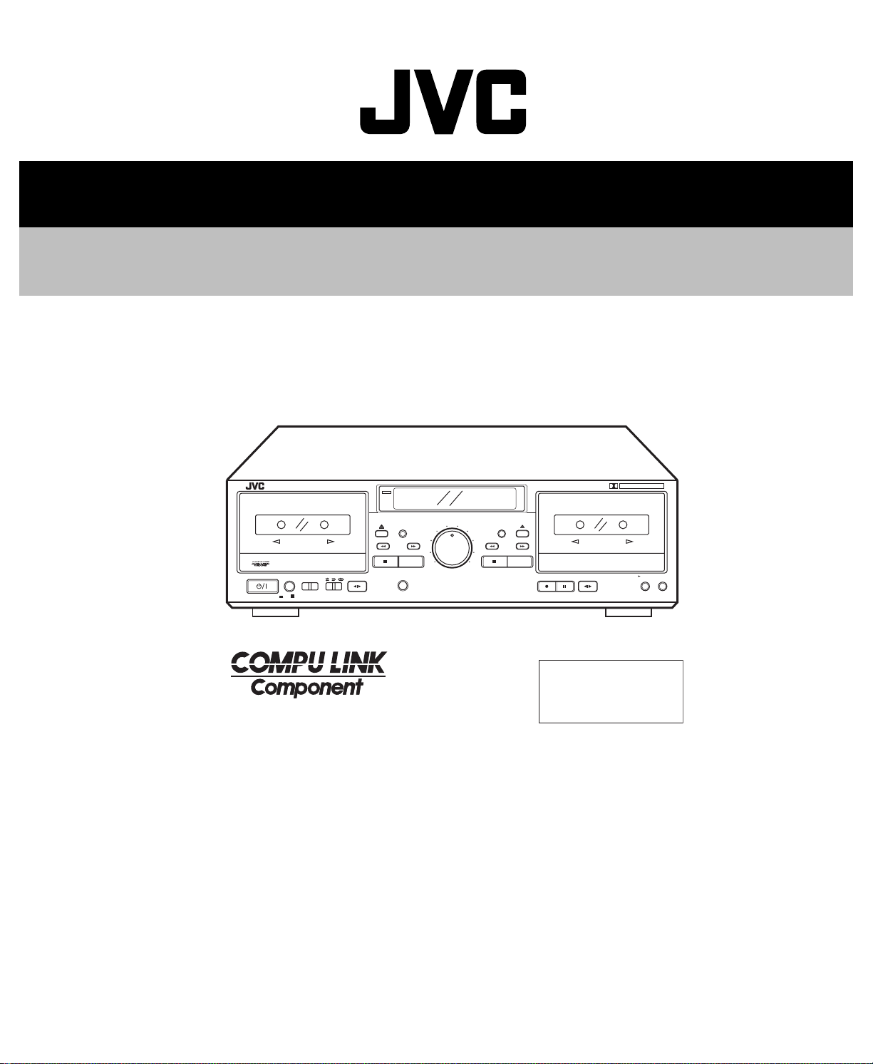
DOUBLE CASSETTE DECK
TD-W271
AUTO REVERSE
A
3MOTOR SILENT MECHANISM
PLAYBACK
POWER
STANDBY/ON ON OFF
DOUBLE CASSETTE DECK
REVERSE MODE
DOLBY NR
B OFF C
STANDBY
COUNTER RESET
PLAY
PHONES
INPUT LEVEL
5
46
37
28
19
MIN MAX
COUNTER RESET
AUTO TAPE SELECTOR / CONTINUOUS PLAY
PLAY
REC / REC MUTE PAUSE
AUTO REVERSE
3MOTOR SILENT MECHANISM
DOLBY B-C NR HX PRO
B
REC/PLAYBACK
A B SYNCHRO DUBBING
NORM SPEED
HIGH SPEED
Area Suffix
UF -------------- China
U -------- Other Areas
TABLE OF CONTENTS
1 PRECAUTION. . . . . . . . . . . . . . . . . . . . . . . . . . . . . . . . . . . . . . . . . . . . . . . . . . . . . . . . . . . . . . . . . . . . . . . . . 1-3
2 SPECIFIC SERVICE INSTRUCTIONS. . . . . . . . . . . . . . . . . . . . . . . . . . . . . . . . . . . . . . . . . . . . . . . . . . . . . . 1-4
3 DISASSEMBLY . . . . . . . . . . . . . . . . . . . . . . . . . . . . . . . . . . . . . . . . . . . . . . . . . . . . . . . . . . . . . . . . . . . . . . . 1-5
4 ADJUSTMENT . . . . . . . . . . . . . . . . . . . . . . . . . . . . . . . . . . . . . . . . . . . . . . . . . . . . . . . . . . . . . . . . . . . . . . . 1-13
5 TROUBLESHOOTING . . . . . . . . . . . . . . . . . . . . . . . . . . . . . . . . . . . . . . . . . . . . . . . . . . . . . . . . . . . . . . . . . 1-19
Page 2
SPECIFICATION
Type Double cassette deck
Track system 4-track, 2-channel
Tape speed 4.8 cm/sec (1-7/8 inch/sec) (Normal)
9.5 cm/sec (3-3/4 inch/sec) (High)
Frequency response
(-20 dB recording)
S/N ratio 58 dB (S = 315 Hz, k3 = 3%, N = A-weighted, Type IV tape)
Improvement of MOL 4 dB at 10 kHz with Dolby C NR on.
Wow and flutter 0.08% (WRMS), ±0.2% (DIN/IEC)
Channel separation 10 dB (1 kHz)
Crosstalk 60 dB (1 kHz)
Harmonic distortion k3; 0.8% (Type IV tape, 315 Hz, 0 VU)
Heads Deck A METAPARM head for playback × 1
Motors Electric govemed DC motor for capstan × 1
Fast forward/rewind time Approx. 110 sec. with C-60 cassette
Input terminals LINE IN (× 1 circuit) Input sensitivity 80 mV (0 VU)
Output terminals LINE OUT (× 1 circuit) Output level 300 mV (0 VU)
Other terminals COMPU LINK-3/SYNCRO × 2
Power requirement AC 220 V, 50 Hz
Power consumption With power on 17 W
Dimensions 435 × 139 331 mm
Mass 5.0 kg
Type IV tape 20-17000Hz
30-16000 Hz (±3dB)
Type II tape 20-16000 Hz
30-15000 Hz (±3dB)
Type I tape 20-16000 Hz
30-15000 Hz (±3dB)
The S/N is improved by about 15 dB at 500 Hz and by max.
20 dB at 1kHz ~ 10 kHz with Dolby C NR on and improved by 5 dB
at 1 kHz and by 10 dB at above 5 k Hz with DOLBY B BR on.
Deck B METAPARM head for recording/playback,
2-gap ferrite head for erasure; combination head × 1
DC motor for reel × 1
DC motor for mechanism drive × 1 (For both decks A and B)
Input impeadance 50 kΩ
Output impeadance 5 kΩ
PHONES × 1 Output level 0.3 mW/8 Ω(0 VU)
Matching impedance 8 Ω - 1 k Ω
With power standby 4.0 W
Design and specifications are subject to change without notice.
1-2 (No.MB061)
Page 3
SECTION 1
PRECAUTION
1.1 Safety Precautions
(1) This design of th is product contains special hardware and
many circuits and components specially for safety purposes. For continued protection, no changes should be made
to the original design unless authorized in writing by the
manufacturer. Replacement parts must be identical to
those used in the original circuits. Services should be performed by qualified personnel only.
(2) Alterations of the design or circuitry of the product should
not be made. Any design alterations of the product should
not be made. Any design alterations or additions will void
the manufacturers warranty and will further relieve the
manufacture of responsibility for personal injury or property
damage resulting therefrom.
(3) Many electrical and mechanical parts in the products have
special safety-related characteristics. These characteristics are often not evident from visual inspection nor can the
protection afforded by them necessarily be obtained by using replacement components rated for higher voltage, wattage, etc. Replacement parts which have these special
safety characteristics are identified in the Parts List of Service Manual. Electrical components having such features
are identified by shading on the schematics and by ( ) on
the Parts List in the Service Manual. The use of a substitute
replacement which does not have the same safety characteristics as the recommended replacement parts shown in
the Parts List of Service Manual may create shock, fire, or
other hazards.
(4) The leads in the products are routed and dressed with ties,
clamps, tubings, barriers and the like to be separated from
live parts, high temperature parts, moving parts and/or
sharp edges for the prevention of electric shock and fire
hazard. When service is required, the original lead routing
and dress should be observed, and it should be confirmed
that they have been returned to normal, after reassembling.
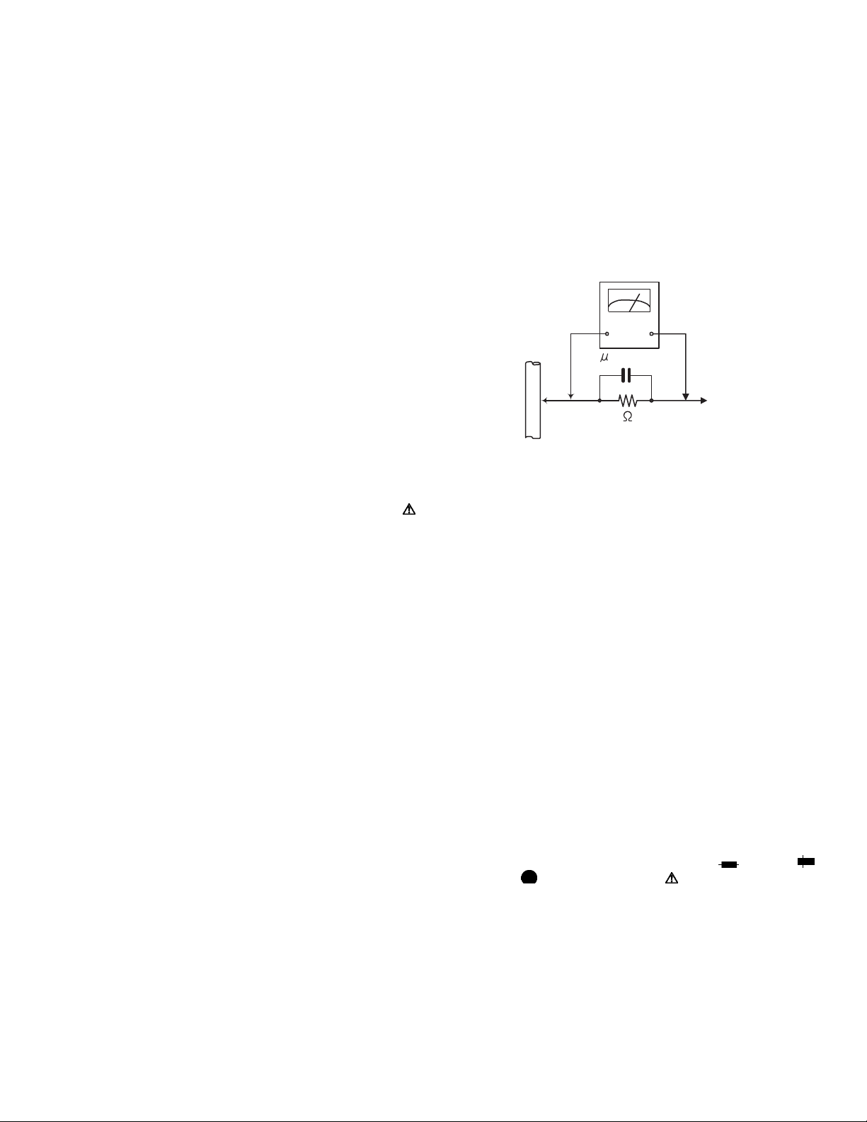
(5) Leakage shock hazard testing
After reassembling the product, always perform an isolation check on the exposed metal parts of the product (antenna terminals, knobs, metal cabinet, screw heads,
headphone jack, control shafts, etc.) to be sure the product
is safe to operate without danger of electrical shock.Do not
use a line isolation transformer during this check.
• P lug the AC line cord directly into the AC outlet. Using a
"Leakage Current Tester", measure the leakage current
from each exposed metal parts of the cabinet, particularly any exposed metal part having a return path to the
chassis, to a known good earth ground. Any leakage current must not exceed 0.5mA AC (r.m.s.).
• Alternate check method
Plug the AC line cord directly into the AC outlet. Use an
AC voltmeter having, 1,000Ω per volt or more sensitivity
in the following manner. Connect a 1,500Ω 10W resistor
paralleled by a 0.15µF AC-type capacitor between an exposed metal part and a known good earth ground.
Measure the AC voltage across the resistor with the AC
voltmeter.
Move the resistor connection to each exposed metal
part, particularly any exposed metal part having a return
path to the chassis, and measure the AC voltage across
the resistor. Now, reverse the plug in the AC outlet and
repeat each measurement. Voltage measured any must
not exceed 0.75 V AC (r.m.s.). This corresponds to 0.5
mA AC (r.m.s.).
AC VOLTMETER
(Having 1000
ohms/volts,
or more sensitivity)
0.15 F AC TYPE
Place this
probe on
1500 10W
Good earth ground
1.2 Warning
(1) This equipment has been designed and manufactured to
meet international safety standards.
(2) It is the legal resp onsibility of the repairer to ensure that
these safety standards are maintained.
(3) Repairs must be made in accordance with the relevant
safety standards.
(4) It is essential that safety critical compone nts are replaced
by approved parts.
(5) If mains voltage selector is provided, check setting for local
voltage.
1.3 Caution Burrs formed during molding may be left over on some parts
of the chassis.
Therefore, pay attention to such burrs in the case of preforming repair of this system.
1.4 Critical parts for safety
In regard with component parts appearing on the silk-screen
printed side (parts side) of the PWB diagrams, the parts that are
printed over with black such as the resistor ( ), diode ( )
and ICP ( ) or identified by the " " mark nearby are critical
for safety. When replacing them, be sure to use the parts of the
same type and rating as specified by the manufacturer.
(This regulation dose not Except the J and C version)
each exposed
metal part.
(No.MB061)1-3
Page 4

SECTION 2
SPECIFIC SERVICE INSTRUCTIONS
This service manual does not describe SPECIFIC SERVICE INSTRUCTIONS.
1-4 (No.MB061)
Page 5
SECTION 3
DISASSEMBLY
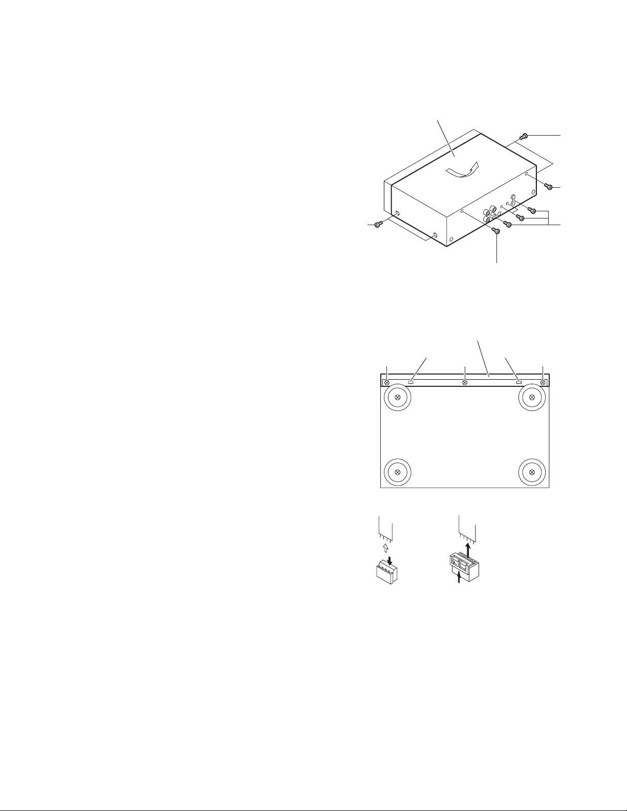
3.1 Enclosure section
3.1.1 Removing the top cover
(See Fig.1)
(1) Remove four screws A retaining the top cover from both
side.
(2) Remove two screws B retaining the top cover from the
back side.
(3) To remove the top cover, slide in direction of arrow and lift
away (refer to Fig.1).
Top cover
A
B
3.1.2 Removing the front panel assembly
(See Fig.2, 3)
(1) Remove the top cover as described in above.
(2) Remove the three screws C retaining the front panel as-
sembly from bottom side.
(3) Release the front panel assembly from two pawls in the
front and bottom sides and draw it to the front side.
(4) Disconnect all connectors between the mechanism assem-
bly, front panel assembly and main board.
A
C
Fig.1
Front panel assembly
Pawl
C C
Fig.2
M
B
Pawl
Pull 2
Push 1
Push up with a screwdriver, etc. 1
Pull 2
Fig.3
(No.MB061)1-5
Page 6
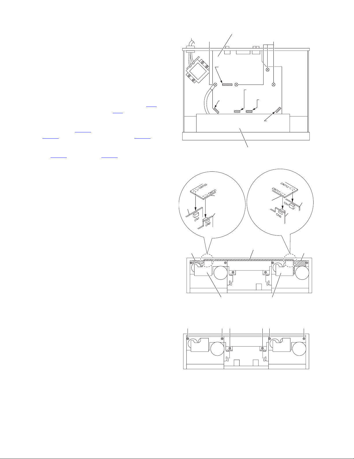
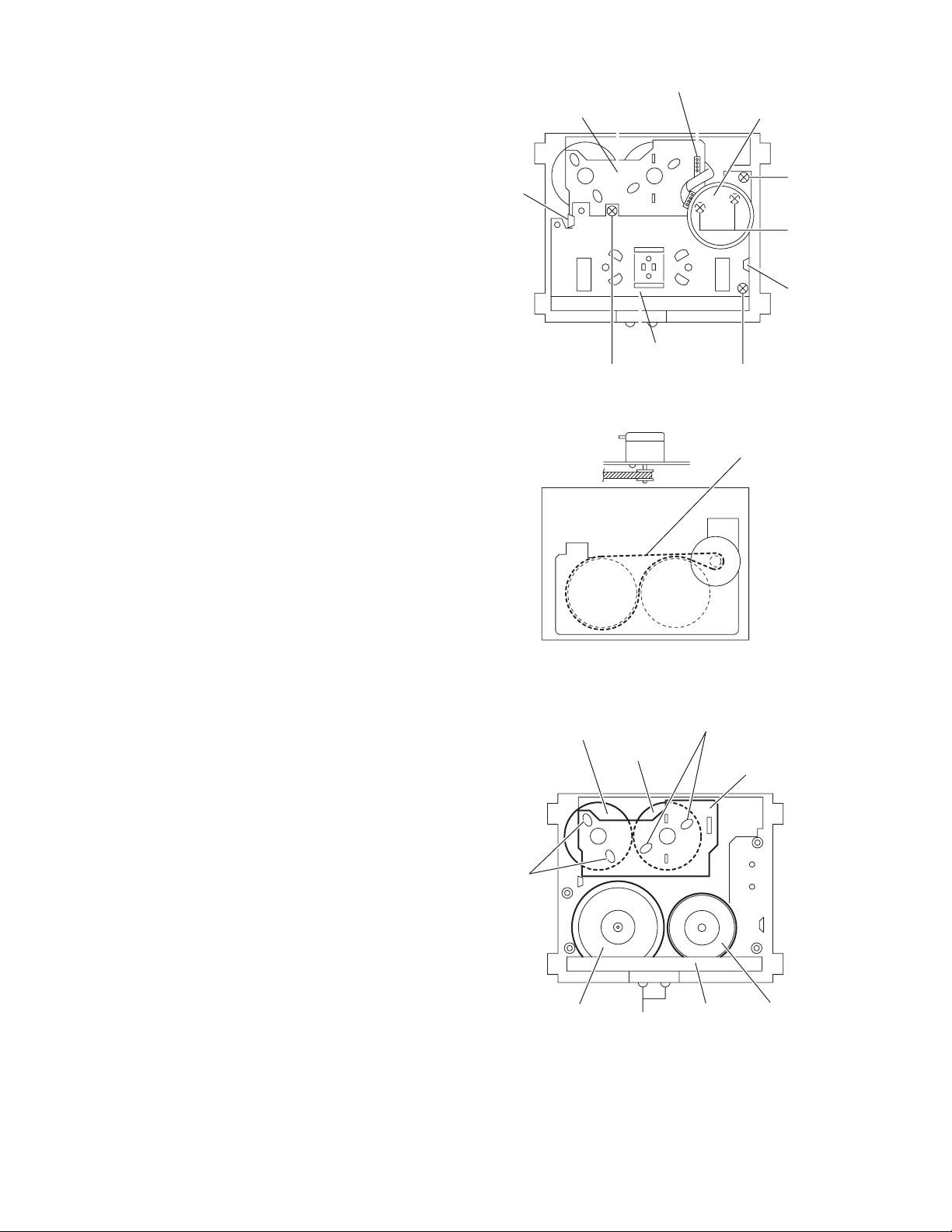
3.1.3 Removing the mechanism assembly
• Although the mechanism assembly can be removed without
detaching the front panel assembly, it is recommended to detach the front panel assembly to do the work with ease.
(1) Remove the two screws D or two screws E from the cor-
ners of the mechanism. (Fig.6)
(2) Open the door and remove the mechanism assembly.
(At this time, door lock arm spring and door lock arm are removed together with.)
(3) For moving the mechanism assembly only, disconnect the
following wirings.
a) Mechanism assembly side (Fig.5)
Top side connector of the cam switch board (CN2
).
Connector of the motor board (CN1). (Board to board
connector)
b) Main board side (Fig.4)
Disconnects CN802
from switch/volume board and CN861 from
CN801
from mecha control board,
headphone jack board.
Disconnect wire coming from the head mount assembly CN811
at deck A and CN815 at deck B.
Remove one screw F and remove one GND wire
from mechanism control board.
3.1.4 Removing the eject arm assembly
(Fig.6)
(1) Remove the screws G retaining the eject arm assembly
and pull it out.
DECK A
Motor
board
Main board
F
From Mechanism
control board
CN802
From DECK A
CN861
CN811
Mechanism control board
Mechanism
control
board
Cam
switch
board
CN801
Fig.4
L
From Headphone jack
board
From Switch/
Volume board
CN815
From DECK B
Mechanism
control
board
DECK B
Motor
board
Cam
switch
board
Motor
board
Mechanism control board
Motor
board
DECK B DECK A
Cam switch board
Cam switch board
Fig.5
DDGGE E
DECK B DECK A
Fig.6
1-6 (No.MB061)
Page 7
3.1.5 Removing the mechanism holder and door assembly
(Fig.7, 8)
(1) Remove four screws H retaining the mechanism holder.
(2) Remove the damper assembly (for easy reassembling
work).
Insert an originary (-) screwdriver or the like in to the gap
between the damper and the front panel to disengage the
pawl, and draw the damper assembly outwards. (See
Fig.7)
(3) Remove the arm shaft of the cassette holder (door assem-
bly) from the mechanism holder. (The door spring is engaged with the door side by the longer side.) (See Fig.8)
(4) Remove the eject spring from lock lever and mechanism
assembly. (See Fig.8)
How to remove damper
Pawl
Fig.7
How to engage the door and eject spring
Lock lever
Cassette door
Longer side
door spring
Shorter side
eject spring
Mechanism assembly
Fig.8
(No.MB061)1-7
Page 8
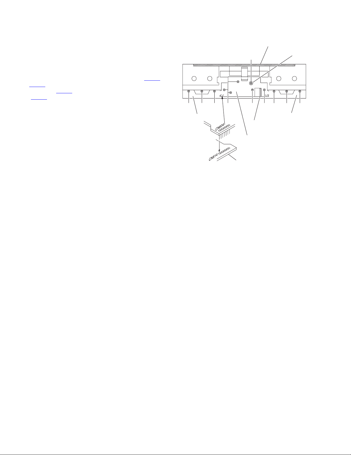
3.1.6 Removing the switch & volume board
(Fig.9)
(1) After removing the mechanism hold er, proceed to the fol-
lowing steps.
(2) Pull out the INPUT volume knob.
(3) Remove four screws J, one screw N and cap retaining the
switch/volume board.
(4) Lift the board right upwards to remove it since it is connect-
ed to the key switch board with connector pins (CN603
).
CN604
(5) Disconnect CN602 coming from Mechanism control board
(CN702
).
3.1.7 Removing the headphone jack board
(Fig.9)
(1) After removing the switch/volume board, pull the head-
phone jack board outwards while pushing it down toward
the bottom side to remove it.
3.1.8 Removing the key switch board
(Fig.9)
(1) Remove one screw K (Deck A or B) retaining the board.
(2) Do the same for the other side.
3.1.9 Removing the main board
(see Fig.4 and 1)
(1) Remove three screws L retaining the board.
(2) Remove four screws M retaining the board to the rear pan-
el.
3.1.10 Reassembling procedure of the front panel assembly
(1) Attach the key switch board to the panel with two screws.
(2) Attach the mechanism holder to the front panel assembly
with four screws.
(3) Put the door assembly on the front panel.
(4) Engage the door spring properly.
(5) Install the damper. (Push the pawl side last to engage it.)
(6) Install the mechanism assembly.
(7) Attach the mechanism control bo ard to the panel with two
screws.
(8) Install the eject arm assembly.
(9) Attach the switch/volume board to the panel with five
screws.
(10) Hook the eject spring between lock lever and mechanism
assembly.
Mechanism control board
N
CN702
/
CN604
Key switch board
CN602
CN603
J
JH HKHKH J
Key witch board
Cap
Headphone jack board
Switch/Volume board
Key switch board
Fig.9
1-8 (No.MB061)
Page 9
3.2 Cassette mechanism section
r
r
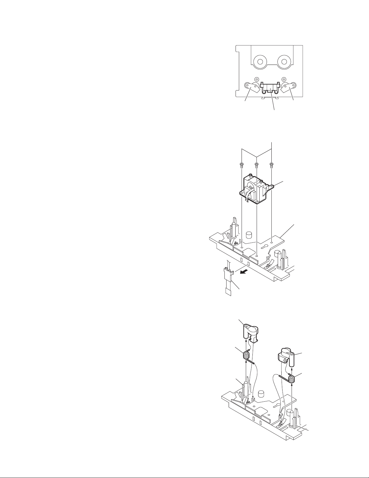
3.2.1 Removing the head mount assembly
(Fig.10 and 11)
(1) Remove the FPC holder from the me chani sm frame in the
direction indicated by the arrow (A).
(2) Remove three screws A retaining the he ad mo unt assem-
bly.
3.2.2 Removing the pinch roller assembly
(Fig.10 and 12)
(1) Remove the pinch roller an d pinch roller spring, refer to
Fig.12.
Mechanism A
Pinch roller (left) Pinch roller (right)
Head mount assembly
Fig.10
A
Head mount assembly
Head base
(A)
FPC Holder
Fig.11
Pinch roller
(left)
Pinch roller
spring
Pawl
Pinch rolle
(right)
Pinch rolle
spring
Pawl
Fig.12
(No.MB061)1-9
Page 10
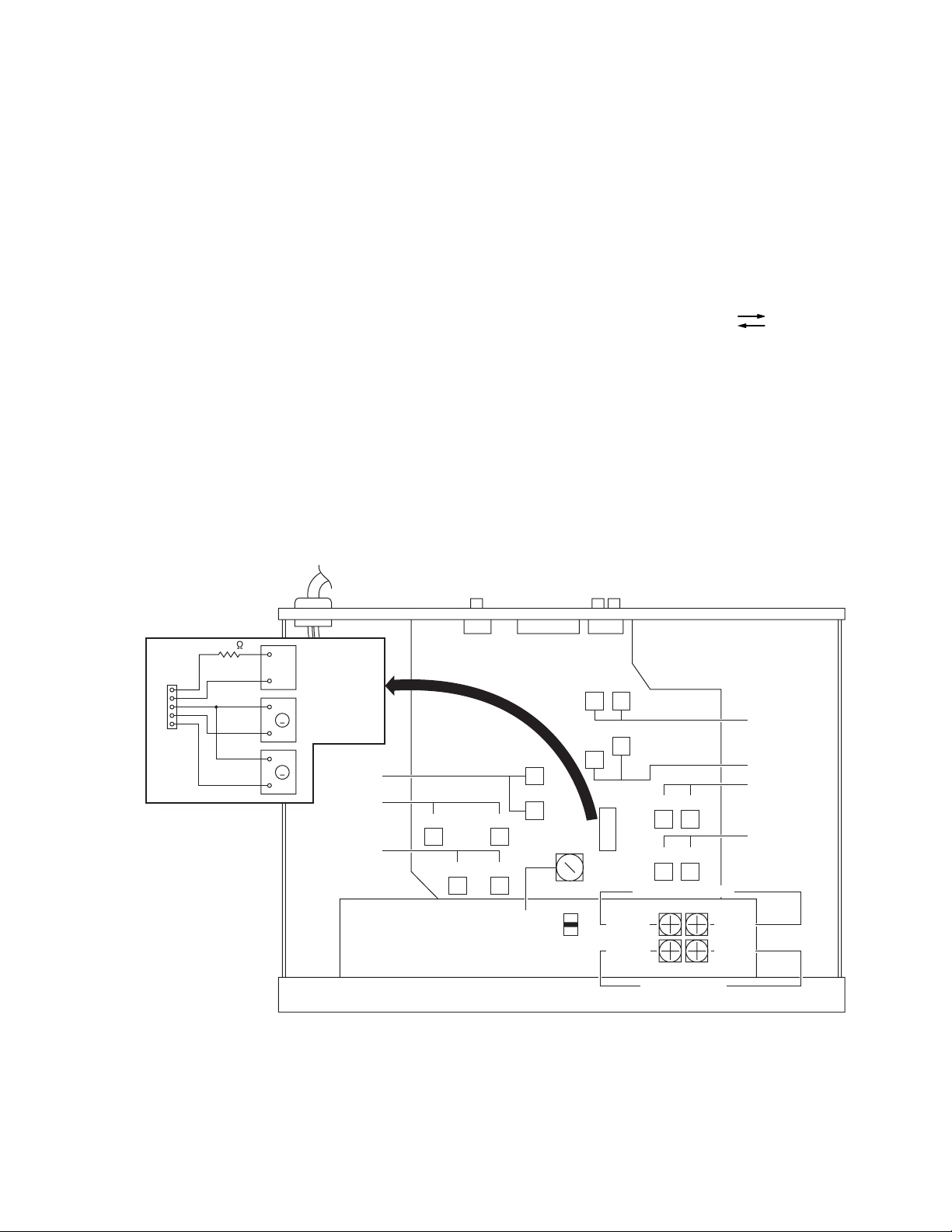
3.2.3 Removing the FM bracket/Capstan motor assembly
(Mechanism A and B)
(1) Remove soldering of connector FM on reel motor board.
(Fig.13)
(2) Remove three screws B and disengage two pawls, and
then the FM bracket and the capstan belt can be removed.
(Fig.13 and 14)
(3) Remove two screws C retaining the capstan motor from the
FM bracket. (Fig.13)
(4) For reengaging the capsta n belt, refer to Fig.14.
Reel motor board
Pawl
Connector FM
FM bracket
B
Fig.13
Capstan motor
B
C
Pawl
B
Capstan belt
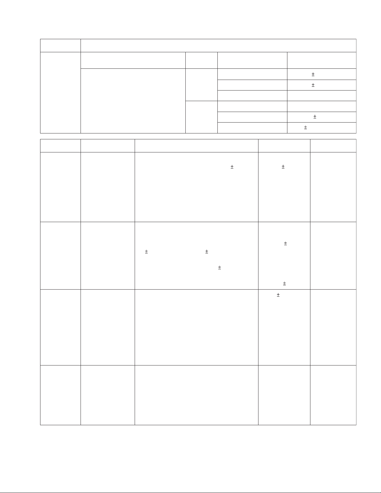
3.2.4 Removing the flywheel assembly
(Fig.15)
(1) Remove two screws D and remove the shield plate.
(2) Pull up the flywheel (L) and (R), and remove them.
3.2.5 Removing the reel motor board
(Fig.15)
(1) Remove four solde ring of the reel motor and actuator mo-
tor, and remove the reel motor board.
Actuator motor
Soldering
Reel motor
Flywheel (R)
Fig.14
Shield plate
D
Fig.15
Soldering
Reel motor board
Flywheel (L)
1-10 (No.MB061)
Page 11

3.2.6 Removing the reel motor assembly
A
(Fig.16)
(1) Remove two screws E from rear of chassis and remove the
reel motor assembly toward upward.
3.2.7 Removing the actuator motor assembly
(Fig.16)
(1) Remove two screws F from rear of chassis and remove the
actuator motor assembly toward upward.
3.2.8 Removing the mechanism board
(Fig.17)
(1) Remove one screw G retaining the board.
(2) Release the mechanism bo ard from five pawls.
(3) For gearing between the mechanism board and control
cam, see the magnified illustration in a circle.
ctuator motor assembly
Reel motor assembly
Mechanism board
EF
Fig.16
Mechanism board
Pawl
Pawl
G
Fig.17
(No.MB061)1-11
Page 12

3.2.9 Removing the control cam
(Fig.18 and 19)
(1) Release the control cam from two pawls. (Fig.18)
(2) For assembling the control cam, fits a zone (groove) of con-
trol cam to a position of pinch lever and b zone (groove) to
b position of head base shaft. (Fig.18 and 19)
3.2.10 Removing the actuator gear A and B (small)
(Fig.18)
(1) Release the actuator gear A (small) from one pawl and re-
move it toward upward.
(2) Release the actuator gear B (small) from one pawl and re-
move it toward upward.
3.2.11 Removing the actuator gear (large)
(Fig.18)
(1) After removing the control cam, actuator gear A (small) and
actuator gear B (small), remove the actuator gear (large).
Actuator gear A
(small)
Pawl
Pawl
Actuator gear
(large)
Control cam
(chassis side)
b
zone
a
zone
Pinch lever Control cam
Actuator gear B
(small)
Head base shaft
Pawl
Fig.18
a
b
Pinch lever
Fig.19
1-12 (No.MB061)
Page 13
SECTION 4
ADJUSTMENT
4.1 Measuring instruments required for adjustment
(1) Low - frequency oscillator (oscillation frequency 50 Hz - 20
kHz, 0 dB output with 600 Ω impedance)
(2) Attenuator (600 Ω impedance)
(3) Electronic voltmeter and oscilloscope
(4) Standard tapes
VT712 (tape speed, wow and flutter measurement)
VT727 (400 Hz reference level)
VT742 (63 Hz, 1 kHz, 12.5 kHz) (play back frequency)
VT705 (12.5 kHz) (azimuth)
(5) Recording reference tapes
AC-225 (Normal), AC-514 (TDK SA) (CrO2)
AC-713 (TDK MA) (Metal)
(6) 600 Ω resistors (for attenuator matching)
(7) Distortion meter (band pass filter)
(8) Torque gauge (cassette) for CTG-N, TW2111, TW2121,
TW2231 and TW2241, mechanism adjustments
(9) Wow & flutter meter
(10) Frequency counter meter
(11) M300 gauge
(12) Band pass filter
4.3 Location of adjustment
4.2 Measurement conditions
(1) Power supply voltage (your local voltage)
AC230 V 50 Hz : B/E/EN version
AC120 V 60 Hz : J/C version
AC230/127/110 V 50/60 Hz : UT/U version
(2) Standard position of the switch and volume knob Switches
and volume knobs setting position
INPUT LEVEL : MAXIMUM
DOLBY NR : OFF
REVERSE MODE :
(3) Standard level (0 dBs) is 0.775 V unless otherwise speci-
fied.
(4) The reference value of recording input level is LINE IN level
of a signal whose LINE OUT level is -8 dBs and H.PHONE
OUT level is -24 dBs.
Connection of CN845
CN845
1
5
470k
(L)
(R)
+
F. COUNTER
(BIAS
GND
FREQUENCY
adj.)
+
DC VOLTMETER
V
(HX PRO adj.)
-
+
V
-
DECK B
REC LEVEL
adj.
DECK A
PB FREQ.
RESPONSE adj.
DECK A
PB LEVEL
adj.
VR211 VR111
LR
VR212 VR112
LR
BIAS
FREQUENCY
VR216
L
VR226
R
VR246 VR146
L2401
L8401
B7101
H.SPEED
TP
R L
L1401
L
R
15
CN845
DECK A
DECK A
VR216 VR116
RRL
VR217 VR117
L
NORMAL SPEED adj.
VR703
VR701
VR704
VR702
HIGH SPEED adj.
DECK B
DECK B
DECK B
REC FREQ.
RESPONSE
adj.
HX PRO adj
DECK B
FREQ.
RESPONSE
adj.
DECK B
PB LEVEL
adj.
(No.MB061)1-13
Page 14

4.4 Mechanism adjustment
Before using test tapes, tape transporting past should be demagnetized.
* Adjustments required after head replacement are marked with an asterisk(*).
Item Conditions Adjustment and Confirmation Standard value Adjust point
* Adjusting
Head
azimuth
Adjusting
tape speed
(motor speed)
Test tape : VT704
or VT705 (12.5 kHz)
1.
Test tape :
VT712 (3 kHz)
After adjustment
of normal speed,
then adjust high
speed.
2.
For high speed
adjustment, set
the deck for play
mode and short
circuit between
B7101 and GND.
Connect an electronic voltmeter to the LINE
1.
OUT terminals.
Play back the VT704 (12.5 kHz) test tape.
2.
Adjust the head angle with the screw (FWD
3.
and REV) until the reading of the electronic
voltmeter becomes maximum for both
channels (phase difference must be "0".)
Repeat the adjustment in FWD and REV
modes as well as for the decks A and B.
4.
1.
Connect a frequency counter to the LINE OUT
terminals.
2.
Perform normal speed adjustment first, and
3.
then do high speed adjustment.
Play back the VT712 test tape.
Adjust for decks A. :
Adjust VR701 for normal speed at 3000 Hz,
and VR702 for high speed at 6000 Hz.
4.
Adjust for decks B. :
Adjust VR703 for normal speed at 3000 Hz,
and VR704 for high speed at 6000 Hz.
Difference in FWD and REV frequencies must
be less than 48 Hz.
Maximum Screws
(FWD, REV)
Deck B
FWD
Deck A
FWD
Normal speed:
Deck A,B ;
3000 15 Hz
High speed:
Deck A,B ;
6000 30 Hz
Deck A :
Normal ; VR701
High ; VR702
Deck B :
Normal ; VR703
High ; VR704
REV Adj.
REV Adj.
Checking
wow and
flutter
Checking
play back
torque
Checking
back
tension
Checking
FF/REW
time
Test tape : VT712 (3
kHz)
1.
Connect a wow and flutter meter to the LINE
OUT terminals.
2.
Play back the VT712 test tape.
3.
Check to see if the reading of the meter is
within 0.17 % (WRMS).
Torque gauge :
TW2111 (FWD)
TW2121 (REV)
Employ a torque testing cassette tape
(TW2111[FWD] / TW2121[REV]) for the
checking, or remove the cassette cover and use
a torque gauge.
Torque gauge :
TW2111 (FWD)
TW2121 (REV)
Employ a torque testing cassette tape
(TW2111[FWD] / TW2121[REV]) for the
checking, play the torque gauge and read the
back tension value to confirm that the back
tension is 1 - 5 g cm.
Tape : AC-225 Play back AC-225 tape in FF/REW mode, check
that the FF/REW time during tape running from
begin to end.
Less than 0.17 %
(WRMS)
27 - 70 g cm
1 - 5 g cm
Less than 120 sec
1-14 (No.MB061)
Page 15
4.5 Electrical adjustment procedure
Item
Checking
1
DOLBY
circuit
(Rec. mode)
(BIAS-CUT)
Signal input: LINE IN Cal. level :
400 Hz, -8 dBs
Output terminal TP : NR IC831 53 and 8
pin.
Check and Adjustment
(Frequency, level)
1 kHz, Cal. - 40 dB
DOLBY B
(Rec)
5 kHz, Cal. - 20 dB
1 kHz, Cal.
1 kHz, Cal. - 40 dB
DOLBY C
(Rec)
5 kHz, Cal. - 20 dB
1 kHz, Cal.
Input signal
Output raise value,
deviation value
+5.7 dB 2 dB
+3.5 dB 1.5 dB
0 dB +0.5 dB -1.0 dB
+16.2 dB +3 dB -2 dB
+2.9 dB 2.5 dB
0 dB 1 dB
Item Conditions Adjustment and Confirmation Standard value Adjust point
*2
Play back
level
adjustment
Test tape :
VT727 (400 Hz)
Play back VT727 in FWD mode, then confirm
that the level at LINE OUT is -4.5 dBs 0.5 dB.
Adjust VR112/VR212 and VR117/VR217 so that
LINE OUT level becomes -4.5 dBs.
Difference level between Lch and Rch must less
than 0.5 dB at LINE OUT.
LINE OUT
-4.5 dBs 0.5 dB
Phone Out
-21 dB
+2.5 dB -1.5 dB
Deck B
L : VR117
R : VR217
Deck A
L : VR112
R : VR212
Confirm that difference playback level between
FWD and REV modes within 1.5 dB.
*3
Play back
frequency
response
adjustment
*4
Bias
frequency
adjustment
*5
Slave
oscillation
(HX PRO)
adjustment
Test tape :
VT742
(63 Hz, 1 kHz,
12.5 kHz)
Frequency counter
TP: CN845 pin 1
Tape: Metal
Mode: REC
Frequency counter
input impedance:
more than 470kohm
(see 3.3 Location of
adjustment.)
DC. Voltmeter
TP: CN845
Lch (pin 3 - 4)
Rch (pin 3 - 5)
Play back VT742 test tape, and adjust VR116,
VR216 (deck B) and VR111, VR211 (deck A) so
that deviation of 12.5 kHz to that of 1kHz is
0.5 0.5 dB (deck A) and 0 0.5 dB (deck B).
Then play back VT742 test tape to confirm that
deviation of 63 Hz to 1 kHz is +2 3 dB.
Connect frequency counter to the pin 1 of CN845
and adjust L8401 so that the counter reads
95 kHz.
This step must be performed after the bias
frequency adjustment.
Load a metal tape and set the deck to the
recording mode.
Adjust L1401 and L2401 to minimize respective
DC voltage of CN845 (pin 3 - 4) at Lch and (pin 3
- 5) at Rch.
Difference level of
12.5 kHz from 1kHz
within 0.5 0.5 dB
(both decks A and
B)
Difference level of
Deck B
L : VR116
R : VR216
Deck A
L : VR111
R : VR211
63 Hz from 1 kHz
within +2 3 dB.
95 kHz 1 kHz Deck B
L8401
Minimum Deck B
L : L1401
R : L2401
(No.MB061)1-15
Page 16

Item Conditions Adjustment and Confirmation Standard value Adjust point
6
Checking
recording
bias current
(Value
appearing
here are
just for
reference
7
Input
sensitivity
level check
*8
REC/PB
frequency
response
adjustment
Measuring point:
Both ends of
100 ohm resistor
connected to the
R/P head terminal
LINE INPUT level:
Ref. -20 dB
(-40 dBs 2 dB)
NR switch : OFF
Connect 100 ohm resistor to the R/P head in
series, and measure voltage at both ends of the
resistor to check to see if measured voltage
meets the following requirements on both
channels.
In recording with metal tape, the bias current
is 1150 uA (1.15 mA).
In recording with CrO
2 tape, the bias current
is 700 uA (0.7 mA).
In recording with normal tape, the bias current
is 590 uA (0.59 mA).
1.
Supply at 1kHz signal to the LINE IN terminals
at -19 dBs, confirm that LINE OUT level is 8dBs.
2.
Confirm that difference level between left and
right within 2 dB.
This step must be performed after the slave
oscillation adjustment.
Record the 1.25 kHz and 12.5 kHz signals at the
level of -20 dB (20 dB lower than the reference
level).
Playing back the recorded signals, adjust VR146
and VR246 so that the level of the 12.5 kHz
signal is 0 0.5 dB to the level of the 1.25 kHz.
Reference values
Metal tape:1150 uA
CrO
2 tape: 700 uA
Normal tape:590 uA
LINE IN:
-19 dBs 2 dB
12.5 kH level:
0 0.5 dB
higher than the
1 kHz level.
Deck B
L : VR146
R : VR246
*9
REC/PB
sensitivity
adjustment
Spec. of freq. area
250 Hz 1 Hz 10 Hz 12.5 Hz
3 dB
NR switch : Off
TAPE switch :
Normal
LINE INPUT level:
Ref. -20 dB
Increase in high
frequencies
Decrease in
high frequencies
5 dB
Response (dB)
0 50 Hz 1 kHz
1.
Apply 400 Hz signal to the LINE IN terminals,
12.5 kHz
record 400 Hz signal at -20 dB input for both
(L and R) channels on a normal tape.
2.
While recording the recorded signal and play it
back, adjust VR126(L) and VR226(R) so that
difference between the recording/playback
level and the reference level is
-28 dBs 0.5 dB on both channels.
Low bias current
Appropriate bias current
High bias current
Frequencies
Normal:
-28 dBs 0.5 dB
CrO
2/Metal:
-28 dBs 1 dB
(Difference between
L and R within
0.5 dB)
Deck B
L : VR126
R : VR226
1-16 (No.MB061)
Page 17

Item Conditions Adjustment and Confirmation Standard value Adjust point
10
Checking
dubbing
calibration
Test tape : VT742
Normal tape :
AC-225
1.
Insert test tape VT742 into deck A and
AC-225 into deck B.
2.
Dubbing the 1kHz signal of VT742 to AC-225
during high speed mode.
Playback the dubbing part of AC-225 (deck B)
and confirm that output level of 1kHz is
-28 dBs +1.5/-2 dB on both channels through
the band pass filter.
11
Maximum
output
check
Checking
12 Record a 1 kHz, -20 dB signal to LINE IN
record/
playback
distortion
Supply 1 kHz signal to the LINE IN terminal in
the Rec. monitoring mode, and read non-clipped
signal level at the LINE IN terminal.
1.
terminals.
2.
Play back the recorded part. Check the output
with a distortion meter to see if the value
conforms to the standard value.
-28 dBs +1.5/-2 dB
LINE OUT:
more than 8 dBs
PHONES OUT:
more than -16 dBs
Normal:
Less than 2 %
CrO
2/Metal:
Less than 3 %
13 Record a 1 kHz, -20 dB signal. Stop the input
Checking
signal to
noise ratio
recording
play back
1.
by disconnecting from the terminal to perform
non-signal recording.
2.
Play back the recorded part. Measure the
-8dBs recording output and the non-signal
recording output for comparison using an
electronic voltmeter. Check to see if the value
conforms to the standard value.
14 Apply a 400 Hz, +20 dB signal to the LINE
Checking
erasing
coefficient
1.
terminals.
2.
Perform recording with the signal enhanced
by 20 dB.
3.
Erase a part of the recording.
4.
Measure the output difference between the
erased part and non-erased part to compare
with an electronic voltmeter.
For the measurement using a metal tape,
connect a band pass filter between the deck and
the electronic voltmeter.
Normal:
More than 40 dB
CrO
2/Metal:
More than 41 dB
LINE OUT:
More than 55 dB
Input
(400 Hz)
(400 Hz)
Band pass filter
Tape deck
(recording,
erasing)
Electronic
voltmeter
(No.MB061)1-17
Page 18

Item Conditions Adjustment and Confirmation Standard value Adjust point
1.
Checking
15
MPX filter
effect
Signal input:
LINE IN
Input level:
Maximum
Connect an electronic voltmeter and
oscilloscope to the LINE OUT terminals.
2.
Set the INPUT volume to the maximum
position.
Supply 1 kHz and 19 kHz signals reference
19 kHz level:
-30 dB (including
18.99 to 19.01 kHz)
lower than 1 kHz
signal
level to the LINE IN terminals respectively in
record/pause mode.
While recording monitor the 1 kHz and 19 kHz
signals respectively, confirm that level
difference between 19 kHz signal to 1 kHz
signal is more than 30 dB.
16 Connect an electronic voltmeter to the LINE
Checking
peak
indicator
calibration
Operation mode:
REC/PAUSE
Input frequency:
1 kHz
Signal input:
LINE IN
LINE OUT: -4 dBs
1.
OUT terminals.
2.
Supply the 1 kHz reference signal (-4 dBs) to
the LINE IN terminals.
3.
While rising the input signal level at the LINE
4.
OUT so that each peak indicator is turned on
with the output level specified on the light.
(Indicator reads at 0
position)
Indicator
- 30
- 20
- 15
- 12
- 10
- 8
- 6
- 4
- 2
0
+ 2
+ 4
+ 6
+ 8
Signal level
(LINE OUT)
- 34 dBs 5 dB
- 24 dBs 4 dB
- 19 dBs 3 dB
- 16 dBs 3 dB
- 14 dBs 2 dB
- 12 dBs 2 dB
- 10 dBs 2 dB
- 8 dBs 1 dB
- 6 dBs 2 dB
- 4 dBs 2 dB
- 2 dBs 2 dB
0 dBs 2 dB
+ 2 dBs 2 dB
+ 4 dBs 2 dB
1-18 (No.MB061)
Page 19

SECTION 5
TROUBLESHOOTING
This service manual does not describe TROUBLESHOOTING.
(No.MB061)1-19
Page 20

VICTOR COMPANY OF JAPAN, LIMITED
AV & MULTIMEDIA COMPANY AUDIO/VIDEO SYSTEMS CATEGORY 10-1,1chome,Ohwatari-machi,Maebashi-city,371-8543,Japan
(No.MB061)
Printed in Japan
WPC
Page 21

SCHEMATIC DIAGRAMS
DOUBLE CASSETTE DECK
TD-W271
CD-ROM No.SML200401
Area suffix
UF ---------------------------- China
U ---------------------- Other Areas
DOUBLE CASSETTE DECK
AUTO REVERSE
A
3MOTOR SILENT MECHANISM
PLAYBACK
REVERSE MODE
DOLBY NR
POWER
B OFF C
STANDBY/ON ON OFF
Contents
Block diagram
Standard schematic diagrams
Printed circuit boards
STANDBY
COUNTER RESET
28
PLAY
PHONES
INPUT LEVEL
5
46
37
19
MIN MAX
COUNTER RESET
AUTO TAPE SELECTOR / CONTINUOUS PLAY
PLAY
REC / REC MUTE PAUSE
AUTO REVERSE
3MOTOR SILENT MECHANISM
DOLBY B-C NR HX PRO
B
REC/PLAYBACK
A B SYNCHRO DUBBING
NORM SPEED
HIGH SPEED
2-1
2-2
2-5 to 7
COPYRIGHT 2004 VICTOR COMPANY OF JAPAN, LTD.
No.MB061SCH
2004/1
Page 22

In regard with component parts appearing on the silk-screen printed side (parts side) of the PWB diagrams, the
parts that are printed over with black such as the resistor ( ), diode ( ) and ICP ( ) or identified by the " "
mark nearby are critical for safety.
(This regulation does not correspond to J and C version.)
Page 23

Block diagram
LINE IN
L
DECK A
PB HEAD
R
L
R
VR111
A PB EQ ADJ
(L)
VR211
A PB EQ ADJ
(R)
2
15 1375
Input Level
VCA
VCA
VR601
Q1101
Q2101
4
D8101
HS
IC851
VOL. CONTROL
& DD RP
DECK A
PB HEAD AMP
4
IC811
6
3
7
A PB LEVEL ADJ
2
8
IC812
PB EQ SWITCH
VR112VR212
(L)(R)
HS
PB SIGNAL
A70
IC818
SELECT
5, 6
Q8172
B PB
1
4 3
2 11 10
8 9
REC IN
12, 13
Q8171
PB IN
A PB
(R)
(L)
REC
1
30 22
28 3
PB IN
PB
IN
OUT
(L)
(L)
IC835
DOLBY NR
REC
OUT
(R)
(R)
15 16
PB OUT
(R)
9
REC
OUT
(L)
HEADPHONES
5
7
IC861
1
3
IC852
LEVEL METER AMP
5
3
L
LINE OUT
R
J8601
H. P. JACK
7
1
DECK B
REC/PB HEAD
ERASE HEAD
L
REC/PB SELECT
VR116
B PB EQ ADJ
(L)
R
IC816
3 1 4
7
VR216
B PB EQ ADJ
(R)
IC845
7
L2401 L1401
8
X
B
HX PRO
2
VR246
BIAS ADJ
-7V -7V
(R)
11
12
10 2
17
VR146
BIAS ADJ
Q8153
9
(L)
REC
DECK B
PB HEAD AMP
VR217
B PB LEVEL ADJ
(R)
FREQUENCY ADJ
4
IC815
7
6
L8401
2
8
3
VR117
B PB LEVEL ADJ
(L)
BIAS OSC
Q8491
Q8492
Q1152
Q2152
B70
Q8481
Q8482
REC AMP
7
IC825
1
REC LEVEL ADJ
+B
-B
Q705
FL MUTE
DI701
Q1251 Q2251
Q8251
REC MUTE
Q706
Q707
5
3
VR226
(R)
VR126
REC LEVEL ADJ
(L)
24
1
2
3
4
5
6
7
9
IC701
G0-G6
S1-S16
47
48
METER
(R)
METER
(L)
2-1
Page 24

Standard schematic diagrams
System control / FL display / Key section
(SHEET 2)
(SHEET 2)
Parts are safety assurance parts.
When replacing those parts make
sure to use the specified one.
SHEET 1
2-2
Page 25

Head amplifier section
Parts are safety assurance parts.
When replacing those parts make
sure to use the specified one.
(SHEET 1)
(SHEET 1)
(SHEET 3)
SHEET 2
2-3
Page 26

Amplifier / Power supply section
(SHEET 2)
2-4
Parts are safety assurance parts.
When replacing those parts make
sure to use the specified one.
SHEET 3
Page 27

Printed circuit boards
Main board
CN861
C8492
C8493
C8495
R8493
CN801
C8494
C2101
R8151
R8152
R1601
R2601
R1603
R1605
C1602
C8602
C2602
R2605
R2603
C2108
C8601
R2102
CN815
Q8163
C1101
VR212
CN811
C8491
C8496
R8491
R1102
C2107
IC816
L8401
C1107
VR112
Q2101
C1102
C2155
R1101
C2102
C1155
VR217
R8492
Q8492
Q8491
C1108
R1159
VR117
R2159
R1109
R2109
IC861
R2101
R2602
Q1101
C1105
R1602
R1604
VR111
C8102
C2105
VR211
C2153
C2254
C1153
L2251
C2256
R2604
IC815
C1151
C2151
C8452
C1452
L1251
C1256
C8151
CN845
C2251
C1103
C2103
R1152
R2152
R1451
D8251
R1271
R2252
C8101
Q8481
C2452
VR116
VR216
R2253
Q8251
IC811
R2104
R1453
R1252
R2451
VR226
R1272
D8101
R8101
C1104
C2104
C8252
Q8253
R1104
R8102
C1254
R2251
C1152
C2152
R8482
C8481
R2257
IC825
Q2251
D8352
R2154
R1273
R2272
Q8352
R1154
R8483
C2451
Q1253
Q2253
C2360
R1105
Q8101
IC812
C8483
R1257
C1251
R8104
C1154
C2154
VR126
R2273
C1360
R1107
R2105
C8482
R8481
C2255
R1106
R1155
R1165
R2165
R2155
R8486
Q8482
R8485
R1253
R1251
D8351
R2107
Q1251
R2271
Q8351
R1108
R2106
R1256
C1359
C1358
C2357
C2358
C2454
C1255
C1357
C2359
C1106
C8152
C2106
C1457
C8251
R8103
R2108
Q1152
Q2152
D8481
C2253
R2256
C1253
R8484
C2453
R1255
R2357
R1158
R2158
R1254
R1357
L2401
C2355
C2356
C1451
R2254
IC835
C1156
C2156
R2255
C1356
R2353
R2160
C8455
C2457
R1258
C1355
R2356
L1401
C2258
L2252
L1252
R1356
R1351
R8354
C1354
R1353
C2354
R2270
C1258
R2351
L2351
R2258
R1160
CN802
C2257
C1257
C2456
C2455
C2259
R2354
C1453
C1454
C1456
R8355
R8351
C1259
C8352
C8351
L1351
IC845
C8451
IC826
R1352 R2352
R2452 R2453
Q2252
R1259
Q1252
C1455
R2259
R1270
R2355
C8901
C8902
R1354 R1355
C8454
R1452
C8453
R1263
C1263
R1262
C1261
R1261
R8353
R8352
C2252
C2267
C1252
R2265
C2265
R2267
R2268
Q8353
VR146
VR246
R8253
IC891
R8505
Q8502
R8451
D8252
R2266
R1264
R8172
Q8501
Q8503 Q8504
R2504
D8514
R8504
R8503
R8501
R8502
C8503
L8402
R8452
R8453
Q8471
R2261
C2266
C2261
C2263
R2264
C2268
Q2261 Q2262
Q1261
R1268
R1267
C1267
C1264
R1266
C1265
R1265
C1262
R8171
IC818
Q8172
R8173
Q8171
C928
R1110
D8451
R8471
R2262
R2263
R2505
R8251
Q1262
C1268
C1266
R8473
Q8252
C2262
C2264
R940
C941
R8472
IC851
R8475
R8252
R1111
C1109
R2111
C2109
R2110
C2351
D8452
R2161
Q915
R8474
R1161
R930
R929
R1505
D8513
R941
C918
C2169
R2516
D926
C2501
C1501
R1504
C924
R1516
D925
C1351
C1169
R8255
C927
Q907
C8501 C8502
D922
D8253
R937
C923
Q908
C2511
C1511
Q912
D921
R928
R938
R927
Q905
D1511
R1515
R1513
C908
R913
C906
D913
R2515
D909
R923
R921
R2511
R8511
Q913
C917
IC852
C8511
D2511
R8516
D907
D910
R8515
C921
C915
C914
C8512
R2512
R2513
D8512
C907
D903
R8514
R914
D914
C904
C8513
R910
D902
IC901
D923
R2514
D908
R902
C902
D924
R908
D8511
C931
C909
R918
Z902
R1512
R1514
R1511
C920
D918
R917
C910
Q2511
C911
R912
Q1511
R1517
R2517
R901
C901
Z901
R1502
R8513
R915
D906
C903
CN901
R2502
Q8511
D901
D917
R2501
R1501
R1503
R2503
D905
D904
Z904
R933
J8501
R8901
J701
Z903
Q901 Q903
Q909
R931
C925
2-5
Page 28

Sub board
W702
R626
R623
CN604
D722
C705
D721
D720
S623
D723
S627
D719
R736
R735
R625
R624
S624
R734
CN722
CN721
IC732
IC734
S626
S625
C734
C733
(Switch/Volume board)
CN602
VR601
D711
D724
R750
VR704
VR703
VR702
R742
VR701
R752
R743
Q742
R751
R745
Q709
Q743
Q741
Q740
R786
CN601
R749
Q708
R741
Q711
R785
R748
R753
R754
D705
Q752
Q744
DI701
D702
R756
C703
Q745
D706
D704
R746
R747
R740
R609
R610
D710
R775
R716
B7101
S606
S607
R719
R774
D708
D707
D703
R773
C706
R608
R772
R771
R607
R669
S608
R670
R770
W703
R652
R671
IC701
R606
R653
R672
R654
R605
R673
R657
R761
D712
S605
R762
S604
R766
R767
CN603
R768
R664
R668
R769
CN702
R665
R666
R667
R659
R702
R661
R662
R663
R658
R660
C701
Q703
D701
R715
R782
X701
R701
C702
Q704
S630
R656
R711
R710
Q707
R712
R628
R655
Q706
S601
R651
R781
CN701
Q705
R627
(A:Key switch board)
(Standby LED board)
FW701
R780
R764
Q712
D713
Q702
R783
(B:Key switch board)
D741
R765
FW701
R708
Q701
R706
R709
R707
Q751
R755
R703
R705
S621 S622 S628 S629
R704
S610
R604
R622
R621
S602
S603
R603
(Headphone jack board)
J8601
IC731
C731
C732
C1601
C2601
IC733
R731
R732
R733
R717
R601
R718
CN614
CN613
C704
D717
D716
CN712
D715
CN711
CN862
D718
R784
Q710
D709
W701
(Mechanism control board)
Trans board (UF version) Trans board (U version)
(Trans board)
(Power switch board)
P1
S901
P3
C900
W2
W3
W2
W3
T901
FW901
C930
W1
Z906 Z905
W2
W3
2-6
(Trans board)(Voltage selector board)
W5
W4
W1
C930
W4
W5
FW901
T901
W2
W3
P3
P1
Page 29

Mechanism board
(Cam switch board) (Motor board)
CN1
S5
S4
B7
B5
B4
S3
B3
S2
B1
S1
IC2
S6
IC1
B8
CN2
FW1
C2
2-7
Page 30

VICTOR COMPANY OF JAPAN, LIMITED
AV & MULTIMEDIA COMPANY AUDIO/VIDEO SYSTEMS CATEGORY 10-1,1chome,Ohwatari-machi,Maebashi-city,371-8543,Japan
(No.MB061SCH)
Printed in Japan
WPC
Page 31

PARTS LIST
[ TD-W271 ]
* All printed circuit boards and its assemblies are not available as service parts.
Area suffix
UF ---------------------------- China
U ---------------------- Other Areas
- Contents -
Exploded view of general assembly and parts list (Block No.M1)
Cassette mechanism assembly and parts list (Block No.MP)
Electrical parts list (Block No.01~03)
Packing materials and accessories parts list (Block No.M3)
No. MB061 3-1
3- 2
3- 5
3- 7
3-12
Page 32

Exploded view of general assembly and parts list
4
4
Block No.
27
M
M
1
M
49
28
48
32
47
A:Mechanism
Ass'y
40
22
45
51
50
22
F
53
41
39
40
19
A:Key switch
board Ass'y
70
30
20
Mechanism control
52
54
37
F
35
36
board Ass'y
60
J
63
34
Q
66
62
33
65
M
4
26
24
4
B
3
24
24
N
27
N
16
24
H
G
13
24
17
Head phone
jack boad
P
25
Switch/Volume board
Ass'y
29
P
42
44
58
44
59
43
44
23
69
44
23
21
21
23
51
61
36
50
46
35
55
E
56
57
38
31
3-2
Page 33

7
6
M
4
4
24
26
24
25
itch/Volume board
Ass'y
5
12
4
8
11
4
A
M
15
9
10
12
77
B
24
3
13
D
14
14
Q
74
18
24
85
12
Power swich
board ass'y
75
P
Main boad Ass'y
13
UF Version
86
83
85
29
51
61
36
50
46
35
55
E
64
48
62
66
65
H
G
22
B:Mechanism
Ass'y
22
72
72
73
J
80
81
71
73
D
87
84
K
76
C
82
L
47
40
49
49
B
L
K
1
A
72
38
57
56
40
31
41
39
B:Key swich board Ass'y
67
68
2
C
67
E
68
3-3
Page 34

General assembly
Block No. [M][1][M][M]
Symbol No.
1 VKL1333-013 CHASSIS BASE
2 VYSR110-016 SPACER
3 QQT0330-003 POWER TRANSF T 901
3 QQT0330-002 POWER TRANSF T 901
4 QYSBST3006Z TAPPING SCREW 3mm x 6mm(x4)
5 VJC2579-005 REAR PANEL
5 VJC2579-004 REAR PANEL
6 QMPR110-200-JN POWER CORD 2m BLACK
6 QMPR490-200-JC POWER CORD 2m BLACK
7 QHS3771-108 CORD STOPPER
8 QYSBSF2608M TAP SCREW M2.6 x 8mm(x2)
9 QYSBSF3008M TAP SCREW 3mm x 8mm(x2)
10 QYSBSF3008M TAP SCREW 3mm x 8mm
11 QYSBSF3008M TAP SCREW 3mm x 8mm
12 QYSBST3006M TAPPING SCREW 3mm x 6mm(x3)
13 QYSBSTG3006Z TAP SCREW M3 x 6mm(x4)
14 QMF51E2-R80-J1 FUSE
15 QMF51E2-R315-J1 FUSE
16 QUQ412-0612CJ FFC WIRE
17 QUQ412-0612CJ FFC WIRE
18 QUQ412-2021CJ FCC WIRE
19 VJG1458-013 FRONT PANEL
19 VJG1458-014 FRONT PANEL
20 VJD5429-002SS JVC MARK
21 VYSA1R4-110 SPACER (x2)
22 QYSBSF3010Z TAP SCREW 3mm x 10mm(x4)
23 QYSBST3006N TAP SCREW M3 x 6mm(x3)
24 QYSBSF2610Z SCREW 2.6mm x 10mm(x6)
25 VYSS201-014 SPACER
26 VYH7979-001MM CAP
27 QYSDST2604Z SCREW 2.6mm x 4mm(x2)
28 VXP5345-003 PUSH BUTTON
29 VXP2131-003 MECHA BUTTON
30 VXP5350-002 MECHA BUTTON
31 VXP3835-003 MECHA BUTTON
32 VXS4398-003 SLIDE KNOB (x2)
33 VKL7856-001 HEAD PHONE BKT
34 VKL6752-001 SNAP PLATE
35 VYH7779-00B DUMPER ASSY (x2)
36 VYSS2R3-024 SPACER (x2)
37 VKW3006-236 TORSION SPRING
38 VKW3006-237 TORSION SPRING
39 VYH2323-001 MECHA HOLDER (x2)
40 QYSBSF2610Z SCREW 2.6mm x 10mm(x4)
41 QYSBSF2610Z SCREW 2.6mm x 10mm(x2)
42 VJT2317-007 CASSETTE HOLDER
43 VJT2317-008 CASSETTE HOLDER
44 VKY4180-401 CASSETTE SPRING (x4)
45 VYH7941-005 LOCK LEVER(L)
46 VYH7941-006 LOCK LEVER(R)
47 VMA4718-001 SHIELD (x2)
48 VKS3655-002 F.P.C. HOLDER (x2)
49 QYSDST2603Z TAP SCREW M2.6 x 3mm(x4)
50 VKW5199-001 TENSION SPRING (x2)
51 VKZ4749-001 SPECIAL SCREW (x2)
52 VKL7293-001SS EJECT SAFTY(R)
53 QYSBSF3010Z TAP SCREW 3mm x 10mm
54 VKW5069-002 TORSION SPRING
55 VKL7663-001 EJECT SAFTY(L)
56 QYSBSF3010Z TAP SCREW 3mm x 10mm
57 VKW5104-003 TORSION SPRING
58 VJT2380-011 CASSETTE LID
59 VJT2380-012 CASSETTE LID
60 VXP5289-007 PUSH BUTTON
61 VXP5289-008 PUSH BUTTON
62 VKW3001-077 SPRING (x2)
63 VKL7857-002 REMOTE ARM
64 VKL7858-002 REMOTE ARM
65 VYH7773-001 BUTTON HOLDER (x2)
66 QYSBSF2610Z SCREW 2.6mm x 10mm(x2)
67 QZF6018-003 FOOT 60mm x 18mm(x4)
68 QYSBST3008Z TH TAP SCREW 3mm x 8mm(x4)
Part No. Part Name Description Local
F901 F902 0.8A
AC250V(x2)
F 903 0.315A
AC250V
W271U
W271UF
W271U
W271UF
W271U
W271UF
W271U
W271U
W271UF
Symbol No.
69 VXL3025-005 KNOB
70 VJK3652-012 FINDER
71 VJG1459-003S TOP COVER
72 E406308-004 SPECIAL SCREW (x4)
73 QYSBST3006M TAPPING SCREW 3mm x 6mm(x2)
74 LV34380-001A NAME PLATE
74 LV34380-002A NAME PLATE
75 QYSPSPD3008Z SCREW 3mm x 8mm(x3)
76 LV30092-0E5A UF LABEL
77 LV43268-001A CCC LABEL
80 VXP5346-002 PUSH BUTTON
81 VKL7859-002 REMOTE BRACKET
82 VYH8119-002 SW BRACKET
83 VKS5569-001 REMOTE BAR
84 VKS5570-001 SLIDER
85 QYSBST3006Z TAPPING SCREW 3mm x 6mm(x3)
86 QYSSST3008Z SCREW 3mm x 8mm
87 QYSDST3006Z TAP SCREW 3mm x 6mm
Part No. Part Name Description Local
W271U
W271UF
W271UF
W271UF
W271UF
W271UF
W271UF
W271UF
W271UF
W271UF
W271UF
W271UF
3-4
Page 35

Cassette mechanism assembly and parts list
NY1000-T1A
NY1000-T1B
Block No.
M
MM
P
28
30
46
13
46
13
47
DECK A
DECK B
13
A
4
45
44
2
14
5
23
3
26
11
1
31
27
29
S5
43
S4
CN1
43
S3
DECK B
S2
S1
37
36
34
34
20
6
35
A
B
S4
40
43
CN1
9
8
43
S2
DECK A
7
39
40
41
42
22
19
16
21
B
B
CN2
38
C2
A
C3
37
C
4.8~5.2
mm
6.2
+
0.2
mm
3-5
Page 36

Cassette mechanism
Block No. [M][P][M][M]
Symbol No.
A VKS3626-00E H.MOUNT ASSY A MECHA
A VKS3629-00E H.MOUNT ASSY B MECHA
B MSN5D257A-SA1 D.C MOTOR ASSY
C MSI5B2LW-SA2 CAPSTAN MOTOR
1 VKS1126-00B CHASSIS BASE
2 VKS5428-00B T-UP REEL ASSY
3 VKW5043-001 B.T. SPRING
4 VKS3617-002 REEL
5 VKW5043-001 B.T. SPRING
6 VKS3627-002 PINCH LEVER
7 VKS2224-002 CONTROL CAM
8 VKS5454-001 ACT GEAR(2) (x2)
9 VKS5455-001 ACT GEAR(3)
11 VKM3632-001 HEAD BASE
13 SDSR2004Z SCREW (x3)
14 VKZ4708-001 SPECIAL SCREW
16 VKS5430-00CMM FR ARM ASSY
19 VKF3195-00A FLY WHEEL(R) ASSY
20 VKF3197-00A FLY WHEEL(L) ASSY
21 MMN-6F4RA38 D.C. MOTOR FOR REEL MOTOR
22 VKS5432-001 REEL MOT. GEAR GEAR KIT S
23 VKZ4705-001 SCREW (x2)
26 VKZ4705-002 SCREW (x2)
27 VKP4227-00B PINCH R.(R)ASSY
28 VKP4229-00B PINCH R.(L)ASSY
29 VKW5045-003 P.R. SP(R) FOR PINCH (R)
30 VKW5046-003 P.R. SP(L) FOR PINCH (L)
31 VKY4670-001 CASSETTE SPRING PRESS KIT S
34 SPSP2603Z SCREW M2.6 x 3mm(x2)
35 VKM3636-002 FM BRACKET
36 VKS5327-005MM THRUST PLATE
37 SBSF2608Z TAPPING SCREW 2.6mm x 8mm(x3)
38 VKB3001-068 BELT
39 SDST2612Z SCREW 2.6mm x 12mm
40 VKS3616-00A CAM SW UNIT S6
41 DN6851-HI HALL IC
42 VKS3630-001MM IC HOLDER IC1
43 MXS00220MVL0 CASSETTE SWITCH A MECHA(x2)
43 MXS00220MVL0 CASSETTE SWITCH S1 S2 S3 S4 S5(x5)
44 VKS3614-001 TURN OVER GEAR
45 VKW5126-001 HEAD SPRING
46 VKZ4730-001 SPECIAL SCREW (x2)
47 VKS3654-001 HEAD MT. COVER
C 2 QFV41HJ-104ZM TF CAPACITOR C2
C 3 QFV41HJ-104ZM TF CAPACITOR C3
CN 1 VMC0234-R15 CONNECTOR CN1
CN 2 VMC0234-R08 CONNECTOR CN2
Part No. Part Name Description Local
3-6
Page 37

Electrical parts list
Main board
Block No. [0][1][0][0]
Symbol No.
IC811 AN6557F IC
IC812 BU4066BC IC
IC815 AN6557F IC
IC816 UPC1330HA IC Head switch
IC818 BU4066BC IC
IC825 BA15218N IC Dual ope amp
IC826 CD4066BE IC
IC835 HA12142NT IC
IC845 UPC1297CA IC
IC851 AN7384N IC
IC852 BA15218N IC Dual ope amp
IC861 BA15218N IC Dual ope amp
IC891 BU2090 IC
IC901 M5218AL IC
Q901 2SD882/QP/ TRANSISTOR
Q903 2SB772/QP/ TRANSISTOR(ACC)
Q905 2SB647/CD/-T TRANSISTOR
Q907 2SC3576-JVC-T TRANSISTOR
Q908 2SC3576-JVC-T TRANSISTOR
Q909 2SD882/QP/ TRANSISTOR
Q912 2SD468/BC/-T TRANSISTOR
Q913 KRA103M-T TRANSISTOR
Q915 2SD468/BC/-T TRANSISTOR
Q1101 KRC103M-T TRANSISTOR
Q1152 2SK301/RS/-T TRANSISTOR
Q1251 KTC3203/OY/-T TRANSISTOR
Q1252 KRC103M-T TRANSISTOR
Q1261 KTC3199/GL/-T TRANSISTOR
Q1262 KRC103M-T TRANSISTOR
Q1511 KTC3203/OY/-T TRANSISTOR
Q2101 KRC103M-T TRANSISTOR
Q2152 2SK301/RS/-T TRANSISTOR
Q2251 KTC3203/OY/-T TRANSISTOR
Q2252 KRC103M-T TRANSISTOR
Q2261 KTC3199/GL/-T TRANSISTOR
Q2262 KRC103M-T TRANSISTOR
Q2511 KTC3203/OY/-T TRANSISTOR
Q8101 KRA103M-T TRANSISTOR
Q8163 KRC103M-T TRANSISTOR
Q8171 KRA103M-T TRANSISTOR
Q8172 KRA103M-T TRANSISTOR
Q8251 KRA103M-T TRANSISTOR
Q8252 KRA103M-T TRANSISTOR
Q8351 KRC103M-T TRANSISTOR
Q8352 KRA103M-T TRANSISTOR
Q8353 KRA103M-T TRANSISTOR
Q8471 KTC3199/GL/-T TRANSISTOR
Q8481 2SC2001/LK/-T TRANSISTOR
Q8482 2SA1175/HFE/-T TRANSISTOR
Q8491 2SC2001/LK/-T TRANSISTOR
Q8492 2SC2001/LK/-T TRANSISTOR
Q8501 KRC103M-T TRANSISTOR
Q8502 KRA103M-T TRANSISTOR
Q8503 KRC103M-T TRANSISTOR
Q8504 KRA103M-T TRANSISTOR
Q8511 2SA1175/HFE/-T TRANSISTOR
D901 11ES2-T4 DIODE
D902 11ES2-T4 DIODE
D903 11ES2-T4 DIODE
D904 11ES2-T4 DIODE
D905 MA700A-T2 SB DIODE
D906 1SS133-T2 DIODE
D907 MTZJ3.6A-T2 ZENER DIODE
D908 1SS133-T2 DIODE
D909 11ES2-T4 DIODE
D910 11ES2-T4 DIODE
D913 MTZJ24D-T2 Z DIODE I/M
D914 1SS133-T2 DIODE
D917 1SS133-T2 DIODE
D918 MTZJ12C-T2 Z DIODE
Part No. Part Name Description Local
Symbol No.
D921 1SS133-T2 DIODE
D922 MTZJ6.2B-T2 Z DIODE
D923 1SS133-T2 DIODE
D924 1SS133-T2 DIODE
D925 1SS133-T2 DIODE
D926 MTZJ6.8B-T2 Z DIODE
D1511 1SS133-T2 DIODE
D2511 1SS133-T2 DIODE
D8101 1SS133-T2 DIODE
D8252 1SS133-T2 DIODE
D8253 1SS133-T2 DIODE
D8351 1SS133-T2 DIODE
D8451 1SS133-T2 DIODE
D8452 1SS133-T2 DIODE
D8481 1SS133-T2 DIODE
D8513 1SS133-T2 DIODE
D8514 1SS133-T2 DIODE
C901 QCF31HZ-103Z C CAPACITOR 0.01uF 50V Z
C902 QCF31HZ-103Z C CAPACITOR 0.01uF 50V Z
C903 QETM1EM-228 E CAPACITOR 2200uF 25V M
C904 QETM1EM-228 E CAPACITOR 2200uF 25V M
C906 QCF31HZ-103Z C CAPACITOR 0.01uF 50V Z
C907 QETN1EM-107Z E CAPACITOR 100uF 25V M
C908 QETN1AM-477Z E CAPACITOR 470uF 10V M
C909 QETN1HM-475Z E CAPACITOR 4.7uF 50V M
C910 QETN1AM-337Z E CAPACITOR 330uF 10V M
C911 QETN1AM-337Z E CAPACITOR 330uF 10V M
C914 QETN1HM-337Z E CAPACITOR 330uF 50V M
C915 QETN1HM-227Z E CAPACITOR 220uF 50V M
C917 QETN1EM-107Z E CAPACITOR 100uF 25V M
C918 QETN1EM-106Z E CAPACITOR 10uF 25V M
C920 QETN1CM-107Z E CAPACITOR 100uF 16V M
C921 QETN1CM-477Z E CAPACITOR 470uF 16V M
C923 QETN1AM-337Z E CAPACITOR 330uF 10V M
C924 QETN1AM-107Z E CAPACITOR 100uF 10V M
C927 QETN1AM-107Z E CAPACITOR 100uF 10V M
C928 QETN1EM-476Z E CAPACITOR 47uF 25V M
C931 QCBB1HK-151Y C CAPACITOR 150pF 50V K
C941 QETN1HM-224Z E CAPACITOR 0.22uF 50V M
C1101 QCBB1HK-471Y C CAPACITOR 470pF 50V K
C1102 QCBB1HK-151Y C CAPACITOR 150pF 50V K
C1103 QCBB1HK-151Y C CAPACITOR 150pF 50V K
C1104 QFLC1HJ-103Z M CAPACITOR 0.01uF 50V J
C1105 QETN1AM-227Z E CAPACITOR 220uF 10V M
C1106 QETN1HM-475Z E CAPACITOR 4.7uF 50V M
C1107 QCBB1HK-471Y C CAPACITOR 470pF 50V K
C1108 QCBB1HK-151Y C CAPACITOR 150pF 50V K
C1151 QFLC1HJ-102Z M CAPACITOR 1000pF 50V J
C1152 QCBB1HK-331Y C CAPACITOR 330pF 50V K
C1153 QCBB1HK-151Y C CAPACITOR 150pF 50V K
C1154 QFLC1HJ-123Z M CAPACITOR 0.012uF 50V J
C1155 QETN1AM-227Z E CAPACITOR 220uF 10V M
C1156 QETN1HM-475Z E CAPACITOR 4.7uF 50V M
C1169 QCBB1HK-271Y C CAPACITOR 270pF 50V K
C1251 QCSB1HJ-330Y C CAPACITOR 33pF 50V J
C1252 QFLC1HJ-472Z M CAPACITOR 4700pF 50V J
C1253 QETN1HM-334Z E CAPACITOR 0.33uF 50V M
C1254 QETN1HM-105Z E CAPACITOR 1uF 50V M
C1255 QCS31HJ-471Z C CAPACITOR 470pF 50V J
C1256 QCS32HJ-151Z C CAPACITOR 150pF 500V J
C1257 QFLC1HJ-123Z M CAPACITOR 0.012uF 50V J
C1258 QFLC1HJ-682Z M CAPACITOR 6800pF 50V J
C1261 QFLC1HJ-822Z M CAPACITOR 8200pF 50V J
C1262 QDX31EM-333Z C CAPACITOR 0.033uF 25V M
C1263 QCB31HK-332Z C CAPACITOR 3300pF 50V K
C1264 QDX31EM-473Z C CAPACITOR 0.047uF 25V M
C1265 QFLC1HJ-682Z M CAPACITOR 6800pF 50V J
C1266 QDX31EM-273Z C CAPACITOR 0.027uF 25V M
C1267 QDX31EM-123Z C CAPACITOR 0.012uF 25V M
C1351 QENC1EM-475Z BP E CAPACITOR 4.7uF 25V M
C1354 QENC1EM-475Z BP E CAPACITOR 4.7uF 25V M
C1355 QFN31HJ-222Z M CAPACITOR 2200pF 50V J
C1356 QFN31HJ-222Z M CAPACITOR 2200pF 50V J
Part No. Part Name Description Local
3-7
Page 38

Symbol No.
Part No. Part Name Description Local
Symbol No.
Part No. Part Name Description Local
C1357 QFN31HJ-222Z M CAPACITOR 2200pF 50V J
C1358 QETN1HM-104Z E CAPACITOR 0.1uF 50V M
C1359 QETN1HM-104Z E CAPACITOR 0.1uF 50V M
C1360 QENC1EM-475Z BP E CAPACITOR 4.7uF 25V M
C1451 QFP32AJ-561Z PP CAPACITOR 560pF 100V J
C1452 QCBB1HK-101Y C CAPACITOR 100pF 50V K
C1453 QCS31HJ-561Z C CAPACITOR 560pF 50V J
C1454 QFN31HJ-103Z M CAPACITOR 0.01uF 50V J
C1455 QFLC1HJ-223Z M CAPACITOR 0.022uF 50V J
C1456 QFLC1HJ-393Z M CAPACITOR 0.039uF 50V J
C1457 QETN1EM-106Z E CAPACITOR 10uF 25V M
C1501 QENC1EM-475Z BP E CAPACITOR 4.7uF 25V M
C1511 QETN1EM-106Z E CAPACITOR 10uF 25V M
C1602 QCB31HK-222Z C CAPACITOR 2200pF 50V K
C2101 QCBB1HK-471Y C CAPACITOR 470pF 50V K
C2102 QCBB1HK-151Y C CAPACITOR 150pF 50V K
C2103 QCBB1HK-151Y C CAPACITOR 150pF 50V K
C2104 QFLC1HJ-103Z M CAPACITOR 0.01uF 50V J
C2105 QETN1AM-227Z E CAPACITOR 220uF 10V M
C2106 QETN1HM-475Z E CAPACITOR 4.7uF 50V M
C2107 QCBB1HK-471Y C CAPACITOR 470pF 50V K
C2108 QCBB1HK-151Y C CAPACITOR 150pF 50V K
C2151 QFLC1HJ-102Z M CAPACITOR 1000pF 50V J
C2152 QCBB1HK-331Y C CAPACITOR 330pF 50V K
C2153 QCBB1HK-151Y C CAPACITOR 150pF 50V K
C2154 QFLC1HJ-123Z M CAPACITOR 0.012uF 50V J
C2155 QETN1AM-227Z E CAPACITOR 220uF 10V M
C2156 QETN1HM-475Z E CAPACITOR 4.7uF 50V M
C2169 QCBB1HK-271Y C CAPACITOR 270pF 50V K
C2251 QCSB1HJ-330Y C CAPACITOR 33pF 50V J
C2252 QFLC1HJ-472Z M CAPACITOR 4700pF 50V J
C2253 QETN1HM-334Z E CAPACITOR 0.33uF 50V M
C2254 QETN1HM-105Z E CAPACITOR 1uF 50V M
C2255 QCS31HJ-471Z C CAPACITOR 470pF 50V J
C2256 QCS32HJ-151Z C CAPACITOR 150pF 500V J
C2257 QFLC1HJ-123Z M CAPACITOR 0.012uF 50V J
C2258 QFLC1HJ-682Z M CAPACITOR 6800pF 50V J
C2261 QFLC1HJ-822Z M CAPACITOR 8200pF 50V J
C2262 QDX31EM-333Z C CAPACITOR 0.033uF 25V M
C2263 QCB31HK-332Z C CAPACITOR 3300pF 50V K
C2264 QDX31EM-473Z C CAPACITOR 0.047uF 25V M
C2265 QFLC1HJ-682Z M CAPACITOR 6800pF 50V J
C2266 QDX31EM-273Z C CAPACITOR 0.027uF 25V M
C2267 QDX31EM-123Z C CAPACITOR 0.012uF 25V M
C2351 QENC1EM-475Z BP E CAPACITOR 4.7uF 25V M
C2354 QENC1EM-475Z BP E CAPACITOR 4.7uF 25V M
C2355 QFN31HJ-222Z M CAPACITOR 2200pF 50V J
C2356 QFN31HJ-222Z M CAPACITOR 2200pF 50V J
C2357 QFN31HJ-222Z M CAPACITOR 2200pF 50V J
C2358 QETN1HM-104Z E CAPACITOR 0.1uF 50V M
C2359 QETN1HM-104Z E CAPACITOR 0.1uF 50V M
C2360 QENC1EM-475Z BP E CAPACITOR 4.7uF 25V M
C2451 QFP32AJ-561Z PP CAPACITOR 560pF 100V J
C2452 QCBB1HK-101Y C CAPACITOR 100pF 50V K
C2453 QCS31HJ-561Z C CAPACITOR 560pF 50V J
C2454 QFN31HJ-103Z M CAPACITOR 0.01uF 50V J
C2455 QFLC1HJ-223Z M CAPACITOR 0.022uF 50V J
C2456 QFLC1HJ-393Z M CAPACITOR 0.039uF 50V J
C2457 QETN1EM-106Z E CAPACITOR 10uF 25V M
C2501 QENC1EM-475Z BP E CAPACITOR 4.7uF 25V M
C2511 QETN1EM-106Z E CAPACITOR 10uF 25V M
C2602 QCB31HK-222Z C CAPACITOR 2200pF 50V K
C8101 QCF31HZ-103Z C CAPACITOR 0.01uF 50V Z
C8102 QCF31HZ-103Z C CAPACITOR 0.01uF 50V Z
C8151 QETN1EM-106Z E CAPACITOR 10uF 25V M
C8152 QCF31HZ-103Z C CAPACITOR 0.01uF 50V Z
C8251 QCF31HZ-103Z C CAPACITOR 0.01uF 50V Z
C8252 QCF31HZ-103Z C CAPACITOR 0.01uF 50V Z
C8351 QETN1AM-477Z E CAPACITOR 470uF 10V M
C8352 QETN1AM-477Z E CAPACITOR 470uF 10V M
C8451 QETN1EM-106Z E CAPACITOR 10uF 25V M
C8452 QCSB1HJ-100Y C CAPACITOR 10pF 50V J
C8453 QETN1HM-105Z E CAPACITOR 1uF 50V M
C8454 QETN1AM-107Z E CAPACITOR 100uF 10V M
C8455 QETN1AM-107Z E CAPACITOR 100uF 10V M
C8481 QETN1HM-475Z E CAPACITOR 4.7uF 50V M
C8482 QETN1AM-107Z E CAPACITOR 100uF 10V M
C8483 QETN1EM-337Z E CAPACITOR 330uF 25V M
C8491 QFP32AJ-103Z PP CAPACITOR 0.01uF 100V J
C8492 QETN1EM-476Z E CAPACITOR 47uF 25V M
C8493 QFLC1HJ-223Z M CAPACITOR 0.022uF 50V J
C8494 QFN31HJ-102Z M CAPACITOR 1000pF 50V J
C8495 QFLC1HJ-152Z M CAPACITOR 1500pF 50V J
C8496 QFLC1HJ-152Z M CAPACITOR 1500pF 50V J
C8501 QETN1AM-107Z E CAPACITOR 100uF 10V M
C8502 QETN1AM-107Z E CAPACITOR 100uF 10V M
C8503 QETN1HM-105Z E CAPACITOR 1uF 50V M
C8511 QCF31HZ-103Z C CAPACITOR 0.01uF 50V Z
C8512 QCF31HZ-103Z C CAPACITOR 0.01uF 50V Z
C8513 QETN1HM-105Z E CAPACITOR 1uF 50V M
C8601 QCF31HZ-103Z C CAPACITOR 0.01uF 50V Z
C8602 QCF31HZ-103Z C CAPACITOR 0.01uF 50V Z
C8901 QCF31HZ-103Z C CAPACITOR 0.01uF 50V Z
R901 QRZ9006-4R7X F.RESISTOR 4.7Ω 1/4W J
R902 QRZ9006-4R7X F.RESISTOR 4.7Ω 1/4W J
R908 QRE141J-181Y C RESISTOR 180Ω 1/4W J
R910 QRE141J-103Y C RESISTOR 10kΩ 1/4W J
R912 QRE141J-103Y C RESISTOR 10k
R913 QRE141J-103Y C RESISTOR 10k
R914 QRE141J-103Y C RESISTOR 10kΩ 1/4W J
R915 QRE141J-103Y C RESISTOR 10kΩ 1/4W J
R917 QRE141J-103Y C RESISTOR 10kΩ 1/4W J
R918 QRE141J-103Y C RESISTOR 10kΩ 1/4W J
R921 QRZ9005-100X FUSI RESISTOR 10
R923 QRJ146J-821X UNF C RESISTOR 820Ω 1/4W J
R927 QRE141J-472Y C RESISTOR 4.7kΩ 1/4W J
R928 QRE141J-472Y C RESISTOR 4.7kΩ 1/4W J
R929 QRE141J-391Y C RESISTOR 390Ω 1/4W J
R930 QRE141J-391Y C RESISTOR 390Ω 1/4W J
R933 QRK126J-271X UNF C RESISTOR 270Ω 1/2W J
R937 QRZ9006-4R7X F.RESISTOR 4.7Ω 1/4W J
R938 QRE141J-331Y C RESISTOR 330Ω 1/4W J
R940 QRZ9031-6R8 FUSI RESISTOR 6.8
R941 QRE141J-471Y C RESISTOR 470Ω 1/4W J
R1101 QRE141J-105Y C RESISTOR 1MΩ 1/4W J
R1102 QRE141J-472Y C RESISTOR 4.7kΩ 1/4W J
R1104 QRE141J-274Y C RESISTOR 270kΩ 1/4W J
R1105 QRE141J-332Y C RESISTOR 3.3kΩ 1/4W J
R1106 QRE141J-472Y C RESISTOR 4.7kΩ 1/4W J
R1107 QRE141J-202Y C RESISTOR 2kΩ 1/4W J
R1108 QRE141J-362Y C RESISTOR 3.6kΩ 1/4W J
R1109 QRE141J-150Y C RESISTOR 15Ω 1/4W J
R1110 QRE141J-333Y C RESISTOR 33kΩ 1/4W J
R1111 QRE141J-123Y C RESISTOR 12kΩ 1/4W J
R1152 QRE141J-472Y C RESISTOR 4.7kΩ 1/4W J
R1154 QRE141J-274Y C RESISTOR 270kΩ 1/4W J
R1155 QRE141J-682Y C RESISTOR 6.8k
R1158 QRE141J-472Y C RESISTOR 4.7kΩ 1/4W J
R1159 QRE141J-150Y C RESISTOR 15
R1160 QRE141J-333Y C RESISTOR 33k
R1161 QRE141J-123Y C RESISTOR 12kΩ 1/4W J
R1165 QRE141J-105Y C RESISTOR 1M
R1251 QRE141J-472Y C RESISTOR 4.7k
R1252 QRE141J-332Y C RESISTOR 3.3kΩ 1/4W J
R1253 QRE141J-333Y C RESISTOR 33k
R1254 QRE141J-123Y C RESISTOR 12kΩ 1/4W J
R1255 QRE141J-822Y C RESISTOR 8.2k
R1256 QRE141J-152Y C RESISTOR 1.5k
R1257 QRE141J-153Y C RESISTOR 15kΩ 1/4W J
R1258 QRE141J-181Y C RESISTOR 180
R1259 QRE141J-105Y C RESISTOR 1M
R1261 QRE141J-562Y C RESISTOR 5.6kΩ 1/4W J
R1262 QRE141J-682Y C RESISTOR 6.8k
R1263 QRE141J-222Y C RESISTOR 2.2k
R1264 QRE141J-222Y C RESISTOR 2.2k
R1265 QRE141J-562Y C RESISTOR 5.6k
R1266 QRE141J-682Y C RESISTOR 6.8kΩ 1/4W J
R1267 QRE141J-182Y C RESISTOR 1.8k
R1270 QRE141J-105Y C RESISTOR 1M
R1273 QRE141J-472Y C RESISTOR 4.7kΩ 1/4W J
R1351 QRE141J-222Y C RESISTOR 2.2k
R1352 QRE141J-103Y C RESISTOR 10k
R1353 QRE141J-472Y C RESISTOR 4.7kΩ 1/4W J
R1354 QRE141J-104Y C RESISTOR 100k
R1355 QRE141J-152Y C RESISTOR 1.5k
Ω
1/4W J
Ω
1/4W J
Ω
Ω
Ω
1/4W J
Ω
1/4W J
Ω
1/4W J
Ω
1/4W J
Ω
1/4W J
Ω
1/4W J
Ω
1/4W J
Ω
1/4W J
Ω
1/4W J
Ω
1/4W J
Ω
1/4W J
Ω
1/4W J
Ω
1/4W J
Ω
1/4W J
Ω
1/4W J
Ω
1/4W J
Ω
1/4W J
Ω
1/4W J
Ω
Ω
1/4W J
1/4W J
3-8
Page 39

Symbol No.
Part No. Part Name Description Local
Symbol No.
Part No. Part Name Description Local
R1356 QRE141J-223Y C RESISTOR 22kΩ 1/4W J
R1357 QRE141J-561Y C RESISTOR 560Ω 1/4W J
R1451 QRE141J-274Y C RESISTOR 270kΩ 1/4W J
R1452 QRE141J-333Y C RESISTOR 33kΩ 1/4W J
R1453 QRJ146J-100X UNF C RESISTOR 10Ω 1/4W J
R1501 QRE141J-393Y C RESISTOR 39k
R1502 QRE141J-124Y C RESISTOR 120k
R1503 QRE141J-102Y C RESISTOR 1kΩ 1/4W J
R1504 QRE141J-183Y C RESISTOR 18kΩ 1/4W J
R1505 QRE141J-222Y C RESISTOR 2.2kΩ 1/4W J
R1511 QRE141J-272Y C RESISTOR 2.7kΩ 1/4W J
R1512 QRE141J-103Y C RESISTOR 10kΩ 1/4W J
R1513 QRE141J-683Y C RESISTOR 68kΩ 1/4W J
R1514 QRE141J-273Y C RESISTOR 27kΩ 1/4W J
R1515 QRE141J-220Y C RESISTOR 22Ω 1/4W J
R1516 QRE141J-102Y C RESISTOR 1kΩ 1/4W J
R1517 QRE141J-222Y C RESISTOR 2.2kΩ 1/4W J
R1601 QRE141J-151Y C RESISTOR 150Ω 1/4W J
R1602 QRE141J-124Y C RESISTOR 120kΩ 1/4W J
R1603 QRE141J-103Y C RESISTOR 10kΩ 1/4W J
R1604 QRE141J-562Y C RESISTOR 5.6k
R1605 QRE141J-182Y C RESISTOR 1.8k
R2101 QRE141J-105Y C RESISTOR 1MΩ 1/4W J
R2102 QRE141J-472Y C RESISTOR 4.7kΩ 1/4W J
R2104 QRE141J-274Y C RESISTOR 270kΩ 1/4W J
R2105 QRE141J-332Y C RESISTOR 3.3kΩ 1/4W J
R2106 QRE141J-472Y C RESISTOR 4.7kΩ 1/4W J
R2107 QRE141J-202Y C RESISTOR 2kΩ 1/4W J
R2108 QRE141J-362Y C RESISTOR 3.6kΩ 1/4W J
R2109 QRE141J-150Y C RESISTOR 15Ω 1/4W J
R2110 QRE141J-333Y C RESISTOR 33kΩ 1/4W J
R2111 QRE141J-123Y C RESISTOR 12kΩ 1/4W J
R2152 QRE141J-472Y C RESISTOR 4.7kΩ 1/4W J
R2154 QRE141J-274Y C RESISTOR 270kΩ 1/4W J
R2155 QRE141J-682Y C RESISTOR 6.8kΩ 1/4W J
R2158 QRE141J-472Y C RESISTOR 4.7kΩ 1/4W J
R2159 QRE141J-150Y C RESISTOR 15Ω 1/4W J
R2160 QRE141J-333Y C RESISTOR 33kΩ 1/4W J
R2161 QRE141J-123Y C RESISTOR 12kΩ 1/4W J
R2165 QRE141J-105Y C RESISTOR 1MΩ 1/4W J
R2251 QRE141J-472Y C RESISTOR 4.7kΩ 1/4W J
R2252 QRE141J-332Y C RESISTOR 3.3kΩ 1/4W J
R2253 QRE141J-333Y C RESISTOR 33kΩ 1/4W J
R2254 QRE141J-123Y C RESISTOR 12kΩ 1/4W J
R2255 QRE141J-822Y C RESISTOR 8.2kΩ 1/4W J
R2256 QRE141J-152Y C RESISTOR 1.5kΩ 1/4W J
R2257 QRE141J-153Y C RESISTOR 15kΩ 1/4W J
R2258 QRE141J-181Y C RESISTOR 180Ω 1/4W J
R2259 QRE141J-105Y C RESISTOR 1MΩ 1/4W J
R2261 QRE141J-562Y C RESISTOR 5.6k
R2262 QRE141J-682Y C RESISTOR 6.8kΩ 1/4W J
R2263 QRE141J-222Y C RESISTOR 2.2k
R2264 QRE141J-222Y C RESISTOR 2.2k
R2265 QRE141J-562Y C RESISTOR 5.6kΩ 1/4W J
R2266 QRE141J-682Y C RESISTOR 6.8k
R2267 QRE141J-182Y C RESISTOR 1.8k
R2270 QRE141J-105Y C RESISTOR 1MΩ 1/4W J
R2273 QRE141J-472Y C RESISTOR 4.7k
R2351 QRE141J-222Y C RESISTOR 2.2kΩ 1/4W J
R2352 QRE141J-103Y C RESISTOR 10k
R2353 QRE141J-472Y C RESISTOR 4.7k
R2354 QRE141J-104Y C RESISTOR 100kΩ 1/4W J
R2355 QRE141J-152Y C RESISTOR 1.5k
R2356 QRE141J-223Y C RESISTOR 22k
R2357 QRE141J-561Y C RESISTOR 560Ω 1/4W J
R2451 QRE141J-274Y C RESISTOR 270k
R2452 QRE141J-333Y C RESISTOR 33k
R2453 QRJ146J-100X UNF C RESISTOR 10Ω 1/4W J
R2501 QRE141J-393Y C RESISTOR 39k
R2502 QRE141J-124Y C RESISTOR 120kΩ 1/4W J
R2503 QRE141J-102Y C RESISTOR 1k
R2504 QRE141J-183Y C RESISTOR 18k
R2505 QRE141J-222Y C RESISTOR 2.2kΩ 1/4W J
R2511 QRE141J-272Y C RESISTOR 2.7k
R2512 QRE141J-103Y C RESISTOR 10k
R2513 QRE141J-683Y C RESISTOR 68kΩ 1/4W J
R2514 QRE141J-273Y C RESISTOR 27k
R2515 QRE141J-220Y C RESISTOR 22
Ω
1/4W J
Ω
Ω
Ω
Ω
Ω
Ω
Ω
Ω
Ω
Ω
1/4W J
Ω
Ω
Ω
1/4W J
Ω
Ω
1/4W J
Ω
1/4W J
Ω
1/4W J
Ω
1/4W J
Ω
Ω
1/4W J
Ω
1/4W J
Ω
1/4W J
1/4W J
1/4W J
1/4W J
1/4W J
1/4W J
1/4W J
1/4W J
1/4W J
1/4W J
1/4W J
1/4W J
1/4W J
1/4W J
R2516 QRE141J-102Y C RESISTOR 1kΩ 1/4W J
R2517 QRE141J-222Y C RESISTOR 2.2kΩ 1/4W J
R2601 QRE141J-151Y C RESISTOR 150Ω 1/4W J
R2602 QRE141J-124Y C RESISTOR 120kΩ 1/4W J
R2603 QRE141J-103Y C RESISTOR 10kΩ 1/4W J
R2604 QRE141J-562Y C RESISTOR 5.6k
R2605 QRE141J-182Y C RESISTOR 1.8k
R8101 QRE141J-223Y C RESISTOR 22kΩ 1/4W J
R8102 QRE141J-104Y C RESISTOR 100kΩ 1/4W J
R8103 QRE141J-102Y C RESISTOR 1kΩ 1/4W J
R8104 QRE141J-473Y C RESISTOR 47kΩ 1/4W J
R8151 QRE141J-223Y C RESISTOR 22kΩ 1/4W J
R8152 QRE141J-223Y C RESISTOR 22kΩ 1/4W J
R8171 QRE141J-102Y C RESISTOR 1kΩ 1/4W J
R8172 QRE141J-104Y C RESISTOR 100kΩ 1/4W J
R8173 QRE141J-104Y C RESISTOR 100kΩ 1/4W J
R8251 QRE141J-102Y C RESISTOR 1kΩ 1/4W J
R8252 QRE141J-104Y C RESISTOR 100kΩ 1/4W J
R8253 QRE141J-223Y C RESISTOR 22kΩ 1/4W J
R8255 QRE141J-223Y C RESISTOR 22kΩ 1/4W J
R8351 QRE141J-183Y C RESISTOR 18k
R8352 QRJ146J-470X UNF C RESISTOR 47Ω 1/4W J
R8353 QRJ146J-470X UNF C RESISTOR 47Ω 1/4W J
R8354 QRE141J-153Y C RESISTOR 15kΩ 1/4W J
R8355 QRE141J-183Y C RESISTOR 18kΩ 1/4W J
R8451 QRE141J-472Y C RESISTOR 4.7kΩ 1/4W J
R8452 QRE141J-362Y C RESISTOR 3.6kΩ 1/4W J
R8453 QRE141J-302Y C RESISTOR 3kΩ 1/4W J
R8471 QRE141J-182Y C RESISTOR 1.8kΩ 1/4W J
R8472 QRE141J-223Y C RESISTOR 22kΩ 1/4W J
R8473 QRE141J-223Y C RESISTOR 22kΩ 1/4W J
R8474 QRE141J-182Y C RESISTOR 1.8kΩ 1/4W J
R8475 QRE141J-473Y C RESISTOR 47kΩ 1/4W J
R8481 QRE141J-103Y C RESISTOR 10kΩ 1/4W J
R8482 QRZ9005-150X FUSI RESISTOR 15
R8483 QRE141J-102Y C RESISTOR 1kΩ 1/4W J
R8484 QRE141J-102Y C RESISTOR 1kΩ 1/4W J
R8485 QRE141J-471Y C RESISTOR 470Ω 1/4W J
R8486 QRE141J-332Y C RESISTOR 3.3kΩ 1/4W J
R8491 QRJ146J-6R8X UNF C RESISTOR 6.8Ω 1/4W J
R8492 QRE141J-823Y C RESISTOR 82kΩ 1/4W J
R8493 QRE141J-823Y C RESISTOR 82kΩ 1/4W J
R8501 QRE141J-103Y C RESISTOR 10kΩ 1/4W J
R8502 QRE141J-683Y C RESISTOR 68kΩ 1/4W J
R8503 QRE141J-103Y C RESISTOR 10kΩ 1/4W J
R8504 QRE141J-103Y C RESISTOR 10kΩ 1/4W J
R8505 QRE141J-103Y C RESISTOR 10kΩ 1/4W J
R8513 QRE141J-223Y C RESISTOR 22kΩ 1/4W J
R8514 QRE141J-103Y C RESISTOR 10kΩ 1/4W J
R8515 QRE141J-101Y C RESISTOR 100
R8516 QRE141J-103Y C RESISTOR 10kΩ 1/4W J
VR111 QVP0004-104Z TRIM RESISTOR 100k
VR112 QVP0004-101Z TRIM RESISTOR 100
VR116 QVP0004-104Z TRIM RESISTOR 100k
VR117 QVP0004-101Z TRIM RESISTOR 100
VR126 QVP0004-203Z TRIM RESISTOR 20k
VR146 QVP0004-203Z TRIM RESISTOR 20k
VR211 QVP0004-104Z TRIM RESISTOR 100k
VR212 QVP0004-101Z TRIM RESISTOR 100
VR216 QVP0004-104Z TRIM RESISTOR 100k
VR217 QVP0004-101Z TRIM RESISTOR 100
VR226 QVP0004-203Z TRIM RESISTOR 20k
VR246 QVP0004-203Z TRIM RESISTOR 20k
L1251 QQL30BJ-183Z COIL 18mH J
L1252 QQL30BJ-472Z COIL 4.7mH J
L1351 QQR0879-001 FILTER
L1401 QQR0847-001 OSC COIL(BIAS)
L2251 QQL30BJ-183Z COIL 18mH J
L2252 QQL30BJ-472Z COIL 4.7mH J
L2351 QQR0879-001 FILTER
L2401 QQR0847-001 OSC COIL(BIAS)
L8401 QQR0845-001 OSC COIL(BIAS)
CN801 QGF1205C1-06 CONNECTOR FFC/FPC (1-6)
CN802 QGF1205C1-20 CONNECTOR FFC/FPC (1-20)
CN811 QGF1220F1-06 CONNECTOR FFC/FPC (1-6)
CN815 QGF1220F1-06 CONNECTOR FFC/FPC (1-6)
Ω
Ω
Ω
1/4W J
Ω
Ω
Ω
Ω
Ω
Ω
Ω
Ω
Ω
Ω
Ω
Ω
Ω
Ω
1/4W J
1/4W J
1/4W J
3-9
Page 40

Symbol No.
Part No. Part Name Description Local
Symbol No.
Part No. Part Name Description Local
CN845 QGA2512C1-05Z CONNECTOR W-B (1-5)
CN861 QGB2003L1-05 CONNECTOR B-B (1-5)
CN901 QGD2501C1-05Z CONNECTOR (1-5)
HS901 VMH4011-201 HEAT SINK
J701 QNS0073-001 JACK
J8501 QNN0135-001 PIN JACK
Z901 QNG0019-001Z FUSE CLIP
Z902 QNG0019-001Z FUSE CLIP
Z903 QNG0019-001Z FUSE CLIP
Z904 QNG0019-001Z FUSE CLIP
Sub board
Block No. [0][2][0][0]
Symbol No.
IC701 MB88514B-1730T IC
IC731 BA6218 IC Motor driver
IC732 BA6218 IC Motor driver
IC733 TA8409S IC Motor driver
IC734 TA8409S IC Motor driver
Q701 KTC3199/GL/-T TRANSISTOR
Q702 KTC3199/GL/-T TRANSISTOR
Q703 KRA103M-T TRANSISTOR
Q704 KTC3199/GL/-T TRANSISTOR
Q705 KTC3199/GL/-T TRANSISTOR
Q706 KTC3199/GL/-T TRANSISTOR
Q707 KTC3199/GL/-T TRANSISTOR
Q708 KRC103M-T TRANSISTOR
Q709 KRC103M-T TRANSISTOR
Q710 KTC3199/GL/-T TRANSISTOR
Q711 KTC3199/GL/-T TRANSISTOR
Q712 KRC103M-T TRANSISTOR
Q740 2SA1175/HFE/-T TRANSISTOR
Q741 2SA1175/HFE/-T TRANSISTOR
Q742 2SA1175/HFE/-T TRANSISTOR
Q743 2SA1175/HFE/-T TRANSISTOR
Q744 KRC103M-T TRANSISTOR
Q745 KRC103M-T TRANSISTOR
Q751 KRC103M-T TRANSISTOR
Q752 KRC103M-T TRANSISTOR
D701 1SS133-T2 DIODE
D702 1SS133-T2 DIODE
D703 1SS133-T2 DIODE
D704 1SS133-T2 DIODE
D705 1SS133-T2 DIODE
D706 1SS133-T2 DIODE
D707 1SS133-T2 DIODE
D708 1SS133-T2 DIODE
D709 1SS133-T2 DIODE
D710 1SS133-T2 DIODE
D711 1SS133-T2 DIODE
D712 1SS133-T2 DIODE
D713 1SS133-T2 DIODE
D715 1SS133-T2 DIODE
D716 1SS133-T2 DIODE
D717 1SS133-T2 DIODE
D718 1SS133-T2 DIODE
D719 1SS133-T2 DIODE
D720 1SS133-T2 DIODE
D721 1SS133-T2 DIODE
D722 1SS133-T2 DIODE
D723 1SS133-T2 DIODE
D724 1SS133-T2 DIODE
D741 SLR-56VC-T12 LED
C701 QETN1AM-107Z E CAPACITOR 100uF 10V M
C702 QCBB1HK-471Y C CAPACITOR 470pF 50V K
C703 QCBB1HK-471Y C CAPACITOR 470pF 50V K
C706 QDXB1CM-472Y C CAPACITOR 4700pF 16V M
C731 QETN1EM-106Z E CAPACITOR 10uF 25V M
C733 QETN1EM-106Z E CAPACITOR 10uF 25V M
Part No. Part Name Description Local
C1601 QCF31HZ-223Z C CAPACITOR 0.022uF 50V Z
C2601 QCF31HZ-223Z C CAPACITOR 0.022uF 50V Z
R601 QRE141J-102Y C RESISTOR 1kΩ 1/4W J
R603 QRE141J-183Y C RESISTOR 18kΩ 1/4W J
R604 QRE141J-273Y C RESISTOR 27k
R605 QRE141J-102Y C RESISTOR 1k
R606 QRE141J-122Y C RESISTOR 1.2kΩ 1/4W J
R607 QRE141J-182Y C RESISTOR 1.8kΩ 1/4W J
R608 QRE141J-272Y C RESISTOR 2.7kΩ 1/4W J
R609 QRE141J-103Y C RESISTOR 10kΩ 1/4W J
R610 QRE141J-103Y C RESISTOR 10kΩ 1/4W J
R621 QRE141J-222Y C RESISTOR 2.2kΩ 1/4W J
R622 QRE141J-182Y C RESISTOR 1.8kΩ 1/4W J
R623 QRE141J-272Y C RESISTOR 2.7kΩ 1/4W J
R624 QRE141J-102Y C RESISTOR 1kΩ 1/4W J
R625 QRE141J-122Y C RESISTOR 1.2kΩ 1/4W J
R626 QRE141J-182Y C RESISTOR 1.8kΩ 1/4W J
R627 QRE141J-272Y C RESISTOR 2.7kΩ 1/4W J
R628 QRE141J-472Y C RESISTOR 4.7kΩ 1/4W J
R651 QRE141J-473Y C RESISTOR 47k
R652 QRE141J-473Y C RESISTOR 47k
R653 QRE141J-473Y C RESISTOR 47kΩ 1/4W J
R654 QRE141J-473Y C RESISTOR 47kΩ 1/4W J
R655 QRE141J-473Y C RESISTOR 47kΩ 1/4W J
R656 QRE141J-473Y C RESISTOR 47kΩ 1/4W J
R657 QRE141J-473Y C RESISTOR 47kΩ 1/4W J
R658 QRE141J-473Y C RESISTOR 47kΩ 1/4W J
R659 QRE141J-473Y C RESISTOR 47kΩ 1/4W J
R660 QRE141J-473Y C RESISTOR 47kΩ 1/4W J
R661 QRE141J-473Y C RESISTOR 47kΩ 1/4W J
R662 QRE141J-473Y C RESISTOR 47kΩ 1/4W J
R663 QRE141J-473Y C RESISTOR 47kΩ 1/4W J
R664 QRE141J-473Y C RESISTOR 47kΩ 1/4W J
R665 QRE141J-473Y C RESISTOR 47kΩ 1/4W J
R666 QRE141J-473Y C RESISTOR 47kΩ 1/4W J
R667 QRE141J-473Y C RESISTOR 47kΩ 1/4W J
R668 QRE141J-473Y C RESISTOR 47kΩ 1/4W J
R669 QRE141J-473Y C RESISTOR 47kΩ 1/4W J
R670 QRE141J-473Y C RESISTOR 47kΩ 1/4W J
R671 QRE141J-473Y C RESISTOR 47kΩ 1/4W J
R672 QRE141J-473Y C RESISTOR 47kΩ 1/4W J
R673 QRE141J-473Y C RESISTOR 47kΩ 1/4W J
R701 QRE141J-153Y C RESISTOR 15kΩ 1/4W J
R702 QRE141J-221Y C RESISTOR 220Ω 1/4W J
R703 QRE141J-471Y C RESISTOR 470Ω 1/4W J
R704 QRE141J-102Y C RESISTOR 1kΩ 1/4W J
R705 QRE141J-102Y C RESISTOR 1kΩ 1/4W J
R706 QRE141J-102Y C RESISTOR 1kΩ 1/4W J
R707 QRE141J-471Y C RESISTOR 470
R708 QRE141J-272Y C RESISTOR 2.7kΩ 1/4W J
R709 QRE141J-103Y C RESISTOR 10k
R710 QRE141J-221Y C RESISTOR 220
R711 QRE141J-473Y C RESISTOR 47kΩ 1/4W J
R712 QRE141J-223Y C RESISTOR 22k
R715 QRE141J-223Y C RESISTOR 22k
R716 QRE141J-102Y C RESISTOR 1kΩ 1/4W J
R717 QRE141J-102Y C RESISTOR 1k
R718 QRE141J-221Y C RESISTOR 220Ω 1/4W J
R719 QRE141J-221Y C RESISTOR 220
R731 QRE141J-332Y C RESISTOR 3.3k
R732 QRE141J-103Y C RESISTOR 10kΩ 1/4W J
R733 QRE141J-182Y C RESISTOR 1.8k
R734 QRE141J-332Y C RESISTOR 3.3k
R735 QRE141J-103Y C RESISTOR 10kΩ 1/4W J
R736 QRE141J-182Y C RESISTOR 1.8k
R740 QRE141J-224Y C RESISTOR 220k
R741 QRE141J-224Y C RESISTOR 220k
R742 QRE141J-153Y C RESISTOR 15k
R743 QRE141J-103Y C RESISTOR 10kΩ 1/4W J
R745 QRE141J-683Y C RESISTOR 68k
R746 QRE141J-224Y C RESISTOR 220k
R747 QRE141J-224Y C RESISTOR 220kΩ 1/4W J
R748 QRE141J-224Y C RESISTOR 220k
R749 QRE141J-224Y C RESISTOR 220k
R750 QRE141J-683Y C RESISTOR 68kΩ 1/4W J
R751 QRE141J-153Y C RESISTOR 15k
R752 QRE141J-103Y C RESISTOR 10k
Ω
1/4W J
Ω
1/4W J
Ω
1/4W J
Ω
1/4W J
Ω
1/4W J
Ω
1/4W J
Ω
1/4W J
Ω
1/4W J
Ω
1/4W J
Ω
1/4W J
Ω
1/4W J
Ω
1/4W J
Ω
1/4W J
Ω
1/4W J
Ω
1/4W J
Ω
Ω
Ω
1/4W J
Ω
1/4W J
Ω
Ω
Ω
Ω
1/4W J
Ω
1/4W J
1/4W J
1/4W J
1/4W J
1/4W J
1/4W J
3-10
Page 41

Symbol No.
R753 QRE141J-224Y C RESISTOR 220kΩ 1/4W J
R754 QRE141J-224Y C RESISTOR 220kΩ 1/4W J
R755 QRZ9031-4R7 FUSI RESISTOR 4.7
R756 QRE141J-103Y C RESISTOR 10kΩ 1/4W J
R761 QRE141J-223Y C RESISTOR 22kΩ 1/4W J
R762 QRE141J-223Y C RESISTOR 22k
R764 QRE141J-103Y C RESISTOR 10k
R765 QRE141J-151Y C RESISTOR 150Ω 1/4W J
R766 QRE141J-682Y C RESISTOR 6.8kΩ 1/4W J
R767 QRE141J-682Y C RESISTOR 6.8kΩ 1/4W J
R768 QRE141J-682Y C RESISTOR 6.8kΩ 1/4W J
R769 QRE141J-682Y C RESISTOR 6.8kΩ 1/4W J
R770 QRE141J-101Y C RESISTOR 100Ω 1/4W J
R771 QRE141J-101Y C RESISTOR 100Ω 1/4W J
R772 QRE141J-101Y C RESISTOR 100Ω 1/4W J
R773 QRE141J-101Y C RESISTOR 100Ω 1/4W J
R774 QRE141J-101Y C RESISTOR 100Ω 1/4W J
R775 QRE141J-101Y C RESISTOR 100Ω 1/4W J
R780 QRE141J-223Y C RESISTOR 22kΩ 1/4W J
R781 QRE141J-223Y C RESISTOR 22kΩ 1/4W J
R782 QRE141J-223Y C RESISTOR 22k
R783 QRE141J-223Y C RESISTOR 22k
R784 QRE141J-223Y C RESISTOR 22kΩ 1/4W J
R785 QRE141J-223Y C RESISTOR 22kΩ 1/4W J
R786 QRE141J-223Y C RESISTOR 22kΩ 1/4W J
VR601 QVGA12B-V06 V RESISTOR
VR701 QVP0077-103Z TRIM RESISTOR 10k
VR702 QVP0077-203Z TRIM RESISTOR 20k
VR703 QVP0077-103Z TRIM RESISTOR 10k
VR704 QVP0077-203Z TRIM RESISTOR 20k
CN601 QGF1205F1-06 CONNECTOR FFC/FPC (1-6)
CN602 QGF1205F1-06 CONNECTOR FFC/FPC (1-6)
CN603 QGG2002M2-06 CONNECTOR (1-6)
CN604 QGG2002M2-04 CONNECTOR (1-4)
CN613 QGB2012J1-06 CONNECTOR B-B (1-6)
CN614 QGB2012J1-04 CONNECTOR B-B (1-4)
CN701 QGF1205F1-20 CONNECTOR FFC/FPC (1-20)
CN702 QGF1205F1-06 CONNECTOR FFC/FPC (1-6)
CN711 QGB1219K1-08S CONNECTOR B-B (1-8)
CN712 QGB1219K1-15S CONNECTOR B-B (1-15)
CN721 QGB1219K1-08S CONNECTOR B-B (1-8)
CN722 QGB1219K1-15S CONNECTOR B-B (1-15)
CN862 QGB2003M2-05 CONNECTOR B-B (1-5)
DI701 QLF0024-001 FL TUBE
J8601 QNS0092-001 JACK
S601 QSW0698-001Z TACT SW
S602 QSW0698-001Z TACT SW
S603 QSS7A23-V03 SLIDE SW
S604 QSW0698-001Z TACT SW
S605 QSW0698-001Z TACT SW
S606 QSW0698-001Z TACT SW
S607 QSW0698-001Z TACT SW
S608 QSW0698-001Z TACT SW
S610 QSS7A23-V03 SLIDE SW
S621 QSW0698-001Z TACT SW
S622 QSW0698-001Z TACT SW
S623 QSW0698-001Z TACT SW
S624 QSW0698-001Z TACT SW
S625 QSW0698-001Z TACT SW
S626 QSW0698-001Z TACT SW
S627 QSW0698-001Z TACT SW
S628 QSW0698-001Z TACT SW
S629 QSW0698-001Z TACT SW
S630 QSW0698-001Z TACT SW
X701 QAX0246-001Z C RESONATOR 8.00MHz
Z701 VYH3844-003 FL HOLDER
Part No. Part Name Description Local
Ω
Ω
1/4W J
Ω
1/4W J
Ω
1/4W J
Ω
1/4W J
Ω
Ω
Ω
Ω
Trans board
Block No. [0][3][0][0]
Symbol No.
C900 QCZ9105-472 C CAPACITOR 4700pF 250V M
C930 QDYB1CM-103Y C CAPACITOR 0.01uF 16V M
P1 QNZ0079-001Z TAB
P1 QNZ0107-001 TAB
P3 QNZ0079-001Z TAB
P3 QNZ0107-001 TAB
S901 QSW0632-001 PUSH SW.
S902 QSW0838-001 VOLTAGE SWITCH
W3 QUB111-14PPPP SIN TWIST WIRE
W3-3 QUB116-10PPPP SIN TWIST WIRE
Z905 QNG0003-001Z FUSE CLIP
Z906 QNG0003-001Z FUSE CLIP
Part No. Part Name Description Local
W271UF
W271U
W271UF
W271U
W271UF
W271UF
W271U
W271U
W271UF
W271U
W271U
3-11
Page 42

Packing materials and accessories parts list
P5
P2
1/2
A1,
A2,A3,
A5,A6,A7
Block No.
M
3
M
M
P2
2/2
2/2
P3
P4
A4
1/2
P3
3-12
P1
Page 43

Packing and accessories
Block No. [M][3][M][M]
Symbol No.
Part No. Part Name Description Local
A 1 LVT1089-001B INST BOOK ENG
A 2 LVT1089-002A INST BOOK CHI
A 2 LVT1089-003A INST BOOK CHI(PEKIN)
A 3 QAM0223-001 PLUG CORD
A 4 QAM0027-002 CONVERSION PLUG
A 5 VMP0088-001JW PIN CORD
A 6 BT-59019-1 WARRANTY CARD
A 7 BT-59021-1 SVC CENTER LIST
P 1 LV34381-001A CARTON BOX
P 2 VPH2480-201 CUSHION (L)
P 3 VPH2480-202 CUSHION (R)
P 4 QPC06006015P ENVELOPE 60cm x 60cm
P 5 VPE3005-007 POLY BAG
W271U
W271U
W271UF
W271U
W271UF
W271UF
3-13
 Loading...