

Page 1
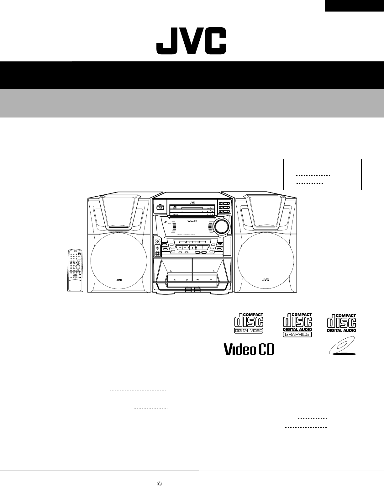
SERVICE MANUAL
COMPACT COMPONENT SYSTEM
MX-J270V
RM-SMXJ111V REMOTE CONTROL
CLOCK
TIMER
1
2 3
–+
SELECT
4 5 6
ECHO SET
7 8 9
10+10
PREV NEXT RETURN SELECT
A – TAPE - B
REC PAUSE
SHIFT FM MODE
SOUND
VOLUME
MODE
MX-J270V
US
UX
STANDBY
PLAY & EXCHANGER
VIDEO CD
1 BIT
DUAL D/A CONVERTER
PHONES
TAPE
MIC LEVEL
AUX
MIN
MAX
ON SCREEN
SLEEP
V.INTRO
HIGHLIGHT
PLAY MODE
CD3CD2CD1
STILL
C D
TAPE
AUX
FM/AM
i
KEY
CONTROL
I
MIC
SP-MXJ270V
NTSC/PAL COMPATIBILITY
MX-J270V
KEY CONTROL
MPX/V.REPLACE/V.MASKING
REC
START/STOP
– PRESET +
NEXT
EJECT EJECT
TUNING / VCD NUMBER
–
SOUND MODE ACTIVE BASS EX.
AUTO REVERSE
DUBBING
CD REC START
PLAY
PREV
REVERSE MODE TAPE A/B
AUTO REVERSE
CA-MXJ270V
ECHO
+
CD
CD
CD
REC/PLAY
NTSC/PAL PAL AUTO
CD
CD
CD
VOLUME
+
–
RANDOM
CD
SELECT
REPEAT
FM /AM
SP-MXJ270V
Area Suffix
Singapore
Saudi Arabia
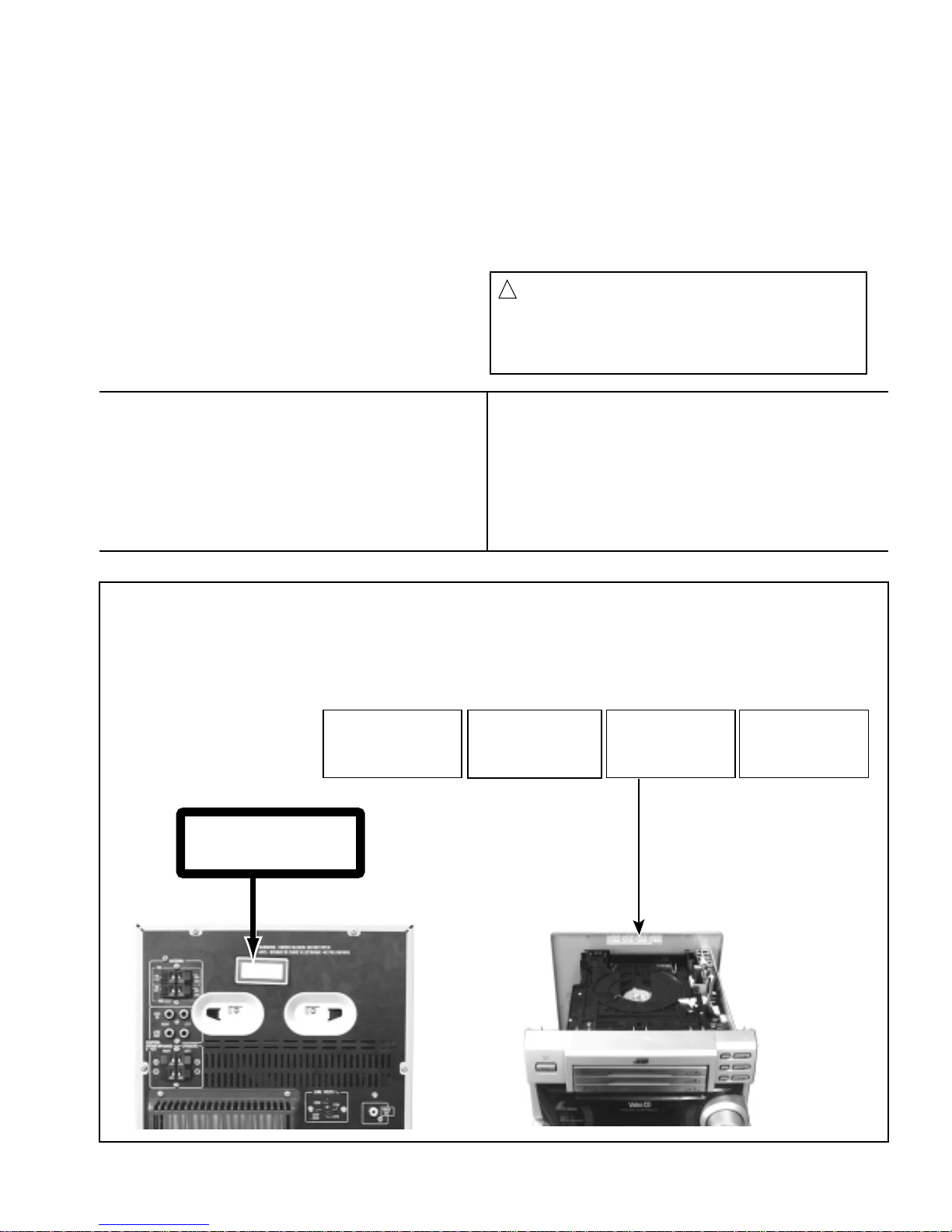
Contents
Safety Precautions
Important for laser products
Preventing static electricity
Disassembly method
Adjustment method
COPYRIGHT 2000 VICTOR COMPANY OF JAPAN, LTD.
1-2
1-3
1-4
1-5
1-22
PlayBack
Control
Flow of functional operation
until TOC read
Maintenance of laser pickup
Replacement of laser pickup
Description of major ICs
VIDEO CD
1-26
1-27
1-27
1-28
No.20880
Nov. 2000
Page 2

MX-J270V
Safety Precautions
1. This design of this product contains special hardware and many circuits and components specially
for safety purposes. For continued protection, no changes should be made to the original design
unless authorized in writing by the manufacturer. Replacement parts must be identical to those
used in the original circuits. Services should be performed by qualified personnel only.
2. Alterations of the design or circuitry of the product should not be made. Any design alterations of
the product should not be made. Any design alterations or additions will void the manufacturer`s
warranty and will further relieve the manufacture of responsibility for personal injury or proper ty
damage resulting therefrom.
3. Many electrical and mechanical par ts in the products have special safety-related characteristics.
These characteristics are often not evident from visual inspection nor can the protection afforded
by them necessarily be obtained by using replacement components rated for higher voltage,
wattage, etc. Replacement parts which have these special safety characteristics are identified in
the Parts List of Service Manual. Electrical components having such features are identified by
shading on the schematics and by ( ) on the Parts List in the Service Manual. The use of a
substitute replacement which does not have the same safety characteristics as the recommended
replacement parts shown in the Parts List of Service Manual may create shock, fire, or other
hazards.
4. The leads in the products are routed and dressed with ties, clamps, tubings, barriers and the
like to be separated from live parts, high temperature parts, moving parts and/or sharp edges
for the prevention of electric shock and fire hazard. When service is required, the or iginal lead
routing and dress should be observed, and it should be confirmed that they have been returned
to normal, after re-assembling.
5. Leakage currnet check (Electrical shock hazard testing)
After re-assembling the product, always perform an isolation check on the exposed metal parts
of the product (antenna terminals, knobs, metal cabinet, screw heads, headphone jack, control
shafts, etc.) to be sure the product is safe to operate without danger of electrical shock.
Do not use a line isolation transformer during this check.
Plug the AC line cord directly into the AC outlet. Using a "Leakage Current Tester", measure
the leakage current from each exposed metal parts of the cabinet , particularly any exposed
metal part having a return path to the chassis, to a known good earth ground. Any leakage
current must not exceed 0.5mA AC (r.m.s.)
Alternate check method
Plug the AC line cord directly into the AC outlet. Use an AC voltmeter having, 1,000 ohms
per volt or more sensitivity in the following manner. Connect a 1,500 10W resistor paralleled by
a 0.15 F AC-type capacitor between an exposed
metal part and a known good earth ground.
Measure the AC voltage across the resistor with the
AC voltmeter.
Move the resistor connection to eachexposed metal
part, par ticularly any exposed metal part having a
return path to the chassis, and meausre the AC
voltage across the resistor. Now, reverse the plug in
the AC outlet and repeat each measurement. voltage
measured Any must not exceed 0.75 V AC (r.m.s.).
This corresponds to 0.5 mA AC (r.m.s.).
0.15 F AC TYPE
1500 10W
Good earth ground
AC VOLTMETER
(Having 1000
ohms/volts,
or more sensitivity)
Place this
probe on
each exposed
metal part.
Warning
1. This equipment has been designed and manufactured to meet international safety standards.
2. It is the legal responsibility of the repairer to ensure that these safety standards are maintained.
3. Repairs must be made in accordance with the relevant safety standards.
4. It is essential that safety critical components are replaced by approved parts.
5. If mains voltage selector is provided, check setting for local voltage.
CAUTION
!
1-2
Burrs formed during molding may be left over on some parts of the chassis. Therefore,
pay attention to such burrs in the case of preforming repair of this system.
Page 3
Important for laser products
MX-J270V
1.CLASS 1 LASER PRODUCT
2.DANGER : Invisible laser radiation when open and inter
lock failed or defeated. Avoid direct exposure to beam.
3.CAUTION : There are no serviceable parts inside the
Laser Unit. Do not disassemble the Laser Unit. Replace
the complete Laser Unit if it malfunctions.
4.CAUTION : The compact disc player uses invisible
laserradiation and is equipped with safety switches
whichprevent emission of radiation when the drawer is
open and the safety interlocks have failed or are de
feated. It is dangerous to defeat the safety switches.
VARNING : Osynlig laserstrålning är denna del är öppnad
och spårren är urkopplad. Betrakta ej strålen.
VARO : Avattaessa ja suojalukitus ohitettaessa olet
alttiina näkymättömälle lasersäteilylle.Älä katso
säteeseen.
5.CAUTION : If safety switches malfunction, the laser is able
to function.
6.CAUTION : Use of controls, adjustments or performance of
procedures other than those specified herein may result in
hazardous radiation exposure.
CAUTION
!
Please use enough caution not to
see the beam directly or touch it
in case of an adjustment or operation
check.
ADVARSEL : Usynlig laserstråling ved åbning , når
sikkerhedsafbrydere er ude af funktion. Undgå
udsættelse for stråling.
ADVARSEL : Usynlig laserstråling ved åpning,når
sikkerhetsbryteren er avslott. unngå utsettelse
for stråling.
REPRODUCTION AND POSITION OF LABELS
WARNING LABEL
DANGER : Invisibie laser radiation
when open and interlock or
defeated.
AVOID DIRECT EXPOSURE TO
BEAM (e)
VARO : Avattaessa ja suojalukitus
ohitettaessa olet alttiina
näkymättömälle lasersäteilylle.Älä
katso säteeseen. (d)
CLASS 1
LASER PRODUCT
VARNING : Osynlig laserstrålning är
denna del är öppnad och spårren är
urkopplad. Betrakta ej strålen. (s)
ADVARSEL :Usynlig laserstråling
ved åbning , når
sikkerhedsafbrydere er ude af
funktion. Undgå udsættelse for
stråling. (f)
1-3
Page 4
MX-J270V
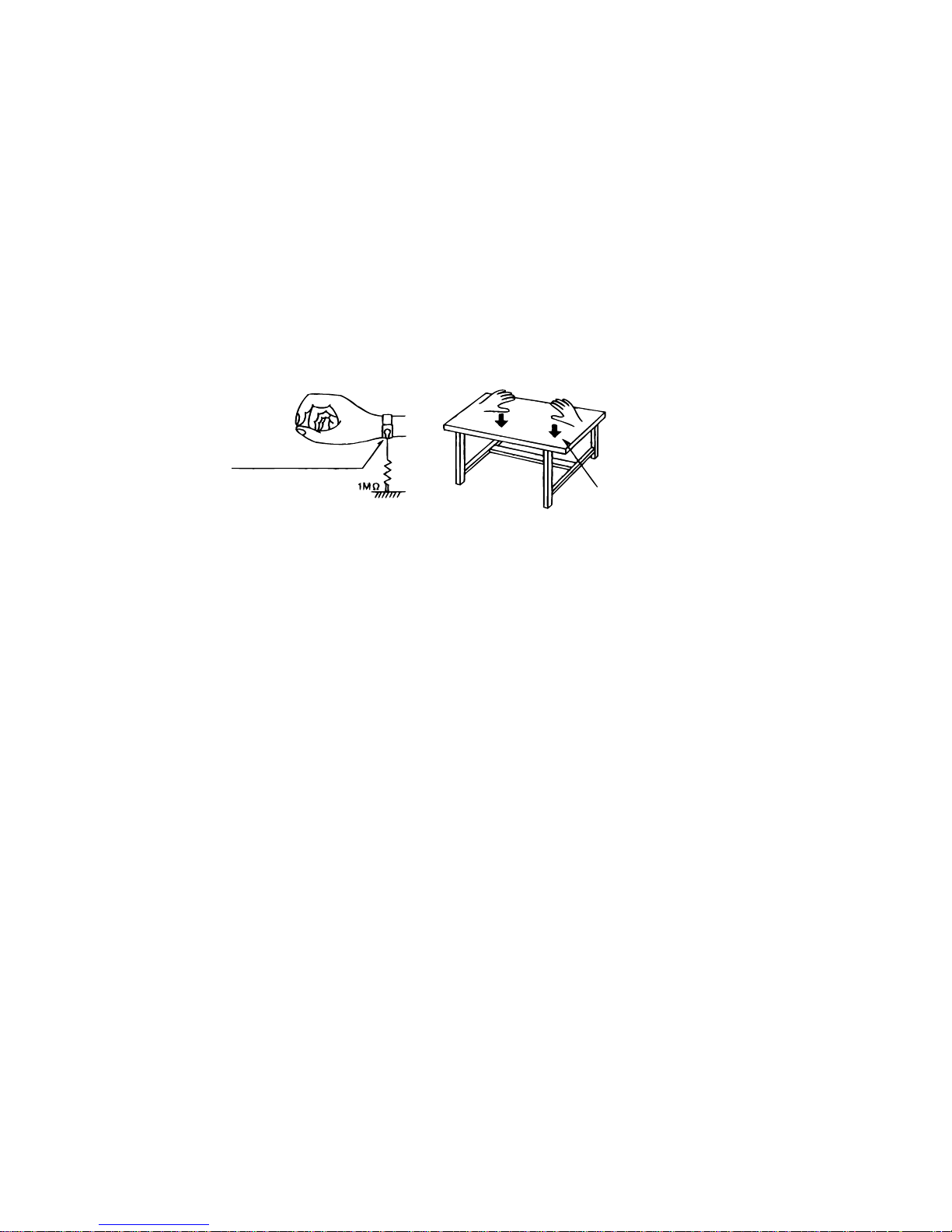
Preventing static electricity
1. Grounding to prevent damage by static electricity
Electrostatic discharge (ESD), which occurs when static electricity stored in the body, fabric, etc. is discharged,
can destroy the laser diode in the traverse unit (optical pickup). Take care to prevent this when performing repairs.
2. About the earth processing for the destruction prevention by static electricity
In the equipment which uses optical pick-up (laser diode), optical pick-up is destroyed by the static electricity of
the work environment.
Be careful to use proper grounding in the area where repairs are being performed.
2-1 Ground the workbench
Ground the workbench by laying conductive material (such as a conductive sheet) or an iron plate over
it before placing the traverse unit (optical pickup) on it.
2-2 Ground yourself
Use an anti-static wrist strap to release any static electricity built up in your body.
(caption)
Anti-static wrist strap
Conductive material
(conductive sheet) or iron plate
3. Handling the optical pickup
1. In order to maintain quality during transport and before installation, both sides of the laser diode on the
replacement optical pickup are shorted. After replacement, return the shorted parts to their original condition.
(Refer to the text.)
2. Do not use a tester to check the condition of the laser diode in the optical pickup. The tester's internal power
source can easily destroy the laser diode.
4. Handling the traverse unit (optical pickup)
1. Do not subject the traverse unit (optical pickup) to strong shocks, as it is a sensitive, complex unit.
2. Cut off the shorted part of the flexible cable using nippers, etc. after replacing the optical pickup. For specific
details, refer to the replacement procedure in the text. Remove the anti-static pin when replacing the traverse
unit. Be careful not to take too long a time when attaching it to the connector.
3. Handle the flexible cable carefully as it may break when subjected to strong force.
4. It is not possible to adjust the semi-fixed resistor that adjusts the laser power. Do not turn it
1-4
Page 5
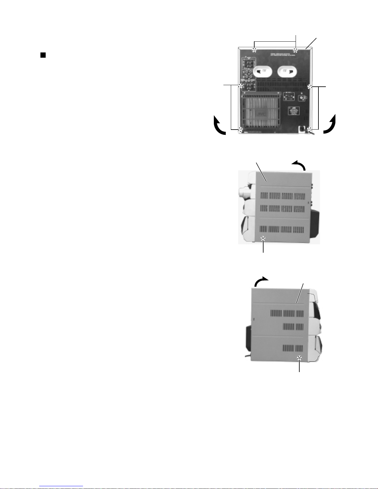
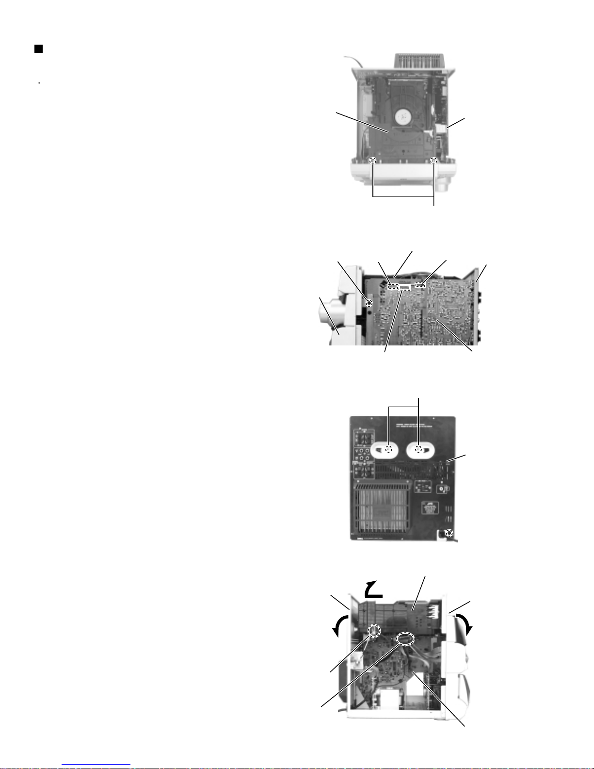
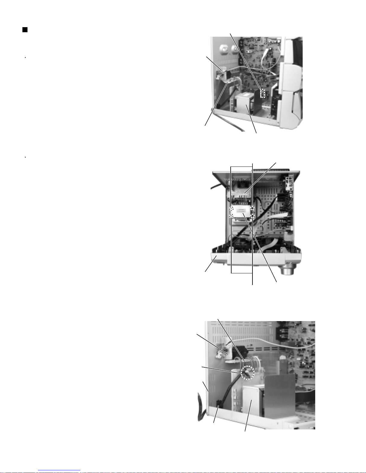
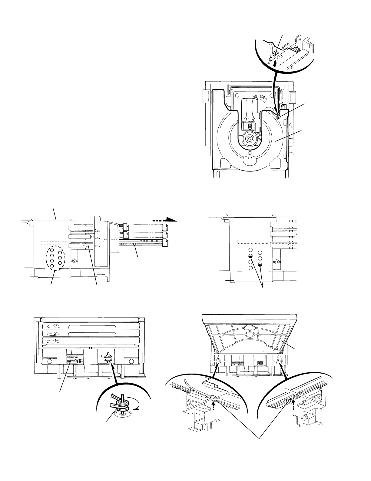
MX-J270V
Remove the six screws A attaching the metal cover
on the back of the body.
Remove the two screws B on both sides of the body.
Remove the metal cover from the body while lifting
up the rear part of the metal cover.
1.
2.
3.
<Main body>
Removing the metal cover
(See Fig.1 to 3)
Disassembly method
Fig.3
Fig.2
Fig.1
Metal cover
A
A
A
Metal cover
B
Metal cover
B
1-5
Page 6
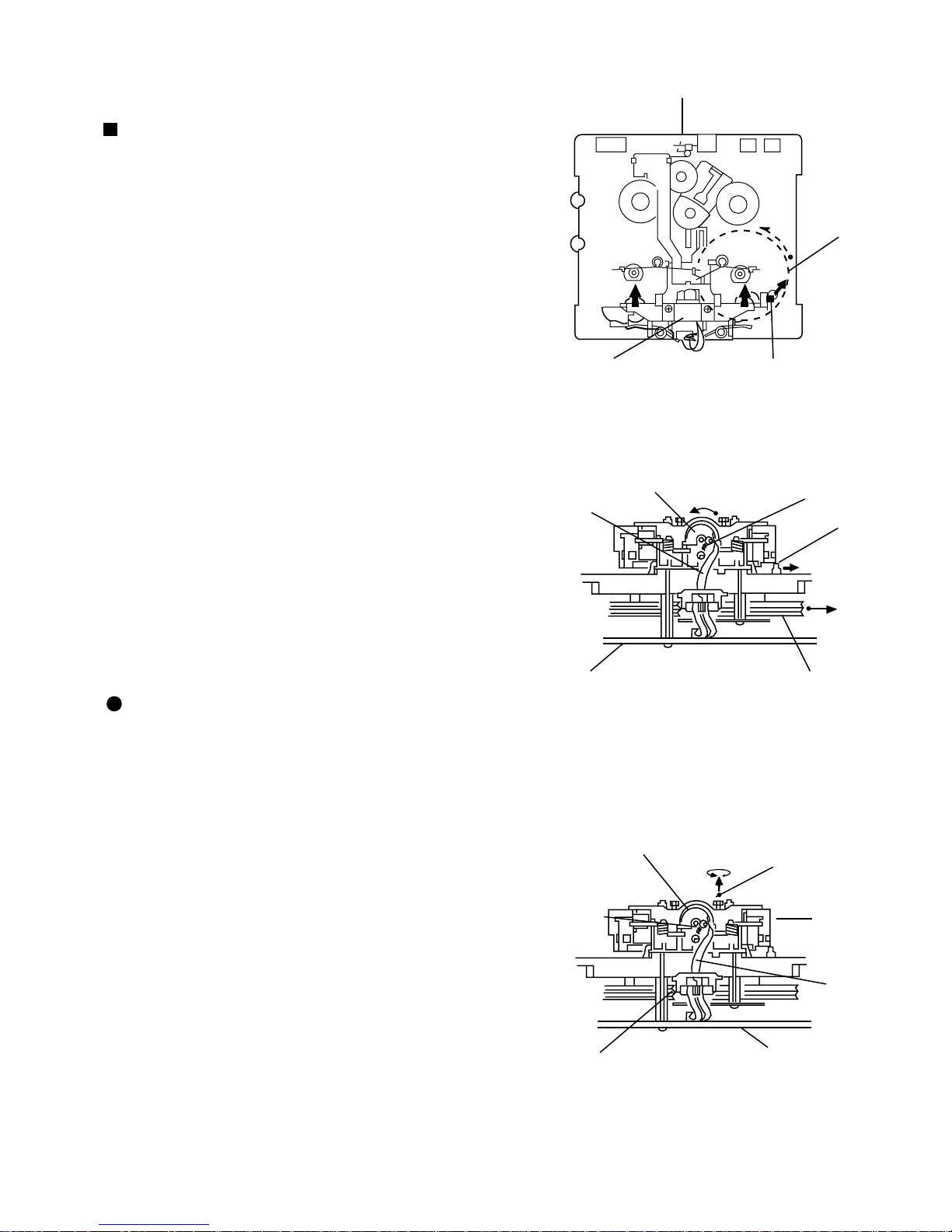
MX-J270V
Removing the CD changer mechanism
assembly (See Fig.4 to 7)
Prior to performing the following procedures, remove
the metal cover.
1.
Disconnect the card wire from connector CN308 and
CN309 connecting the CD servo board and the main
board.
2.
Disconnect the harness from CN310 on the main
board.
3.
Remove the two screws C attaching the CD changer
mechanism assembly on the top of the body.
4.
Remove the plastic rivet a fixing the main board to
the front panel assembly on the left side of the body.
5.
Remove the two screws D from the rear panel.
6.
Cut off the band b and band c which bundle two
harnesses coming from the MIC/headphone board
and one harness coming from the video board,
respectively.
CD changer
mechanism
assembly
Plastic rivet a
Front panel
assembly
Main board
CN303
C
Fig.4
CD changer mechanism assembly
CN310
CN308
Rear panel
7.
Detach upward the rear part of the CD changer
mechanism assembly while pulling the front panel
assembly and the rear panel outward, then pull out
the front part backward and upward.
Rear panel
CN309
Main board
Fig.5
D
Rear panel
Fig.6
CD changer mechanism
assembly
Front panel
assembly
1-6
Pull outward
Band b
Band c
Fig.7
Pull outward
Main board
Page 7
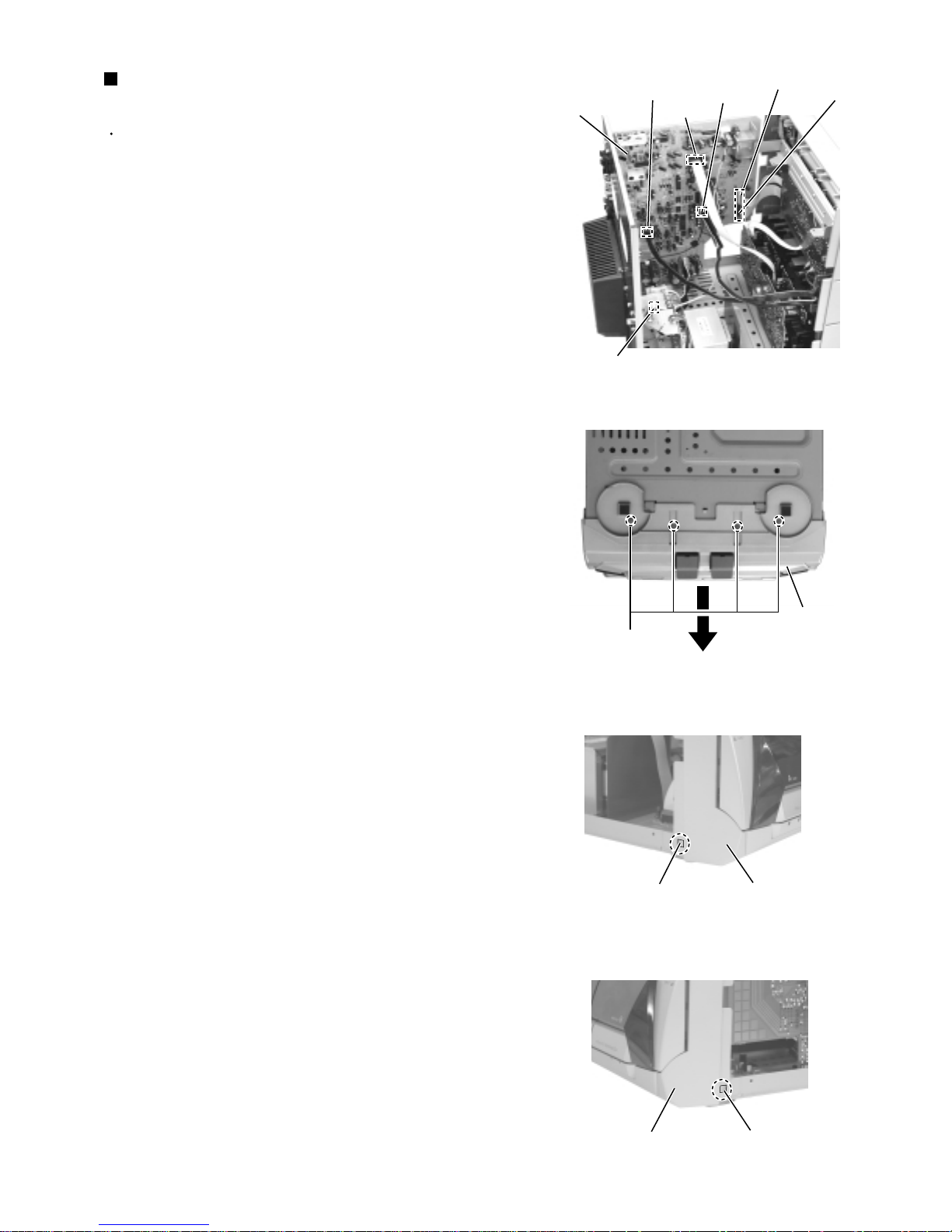
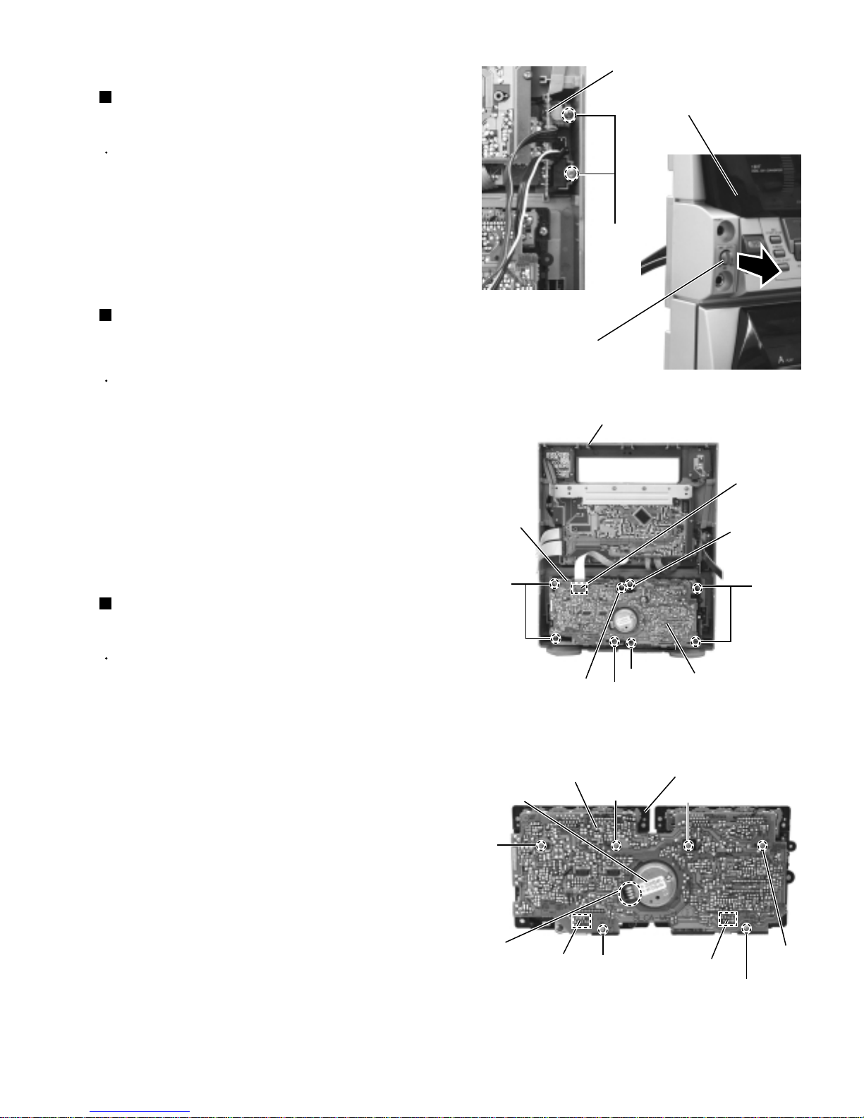
MX-J270V
Prior to performing the following procedures, remove
the metal cover and the CD changer mechanism
assembly.
Disconnect the card wires from connector CN302,
CN306, CN307 and the harness from CN301,
CN305 on the inside of the main board.
Turn over the body and remove the four screws E.
Release the joint d and e on both sides of the body
using a screwdriver, and detach the front panel
assembly toward the front.
1.
2.
3.
Removing the front panel assembly
(See Fig.8 to 11)
Fig.9
Fig.8
Fig.10
Fig.11
Main board
CN301
CN302
CN306
CN307
CN312
CN305
E
Front panel
assembly
Front panel
assembly
Joint d
Front panel
assembly
Joint e
(Bottom)
1-7
Page 8
MX-J270V
Removing the rear cover, the rear panel,
the voltage selector and the video board
(See Fig.12 to 15)
Prior to performing the following procedures, remove
the metal cover and the CD changer mechanism
assembly.
It is not necessary to remove the front panel
assembly.
1.
Remove the two screws F and the rear cover on the
back of the body.
2.
Remove the four screws G and the seven screws H
attaching the main board and the heat sink to the
rear panel.
3.
Remove the screw I attaching the rear panel to the
chassis base.
4.
Remove the two screws J attaching the rear panel to
the voltage selector.
5.
Remove the two screws K attaching the rear panel to
the video board.
F
Rear cover
H
G
(To Earth bracket)
H
Rear panel
F
Fig.12
Rear panel
J
K
6.
Release the lower two joints f and g on both sides of
the rear panel using a screwdriver and detach the
rear panel backwards.
Rear panel
G
I
Fig.13
Joint f
Fig.14
1-8
Rear panel
Joint g
Fig.15
Page 9
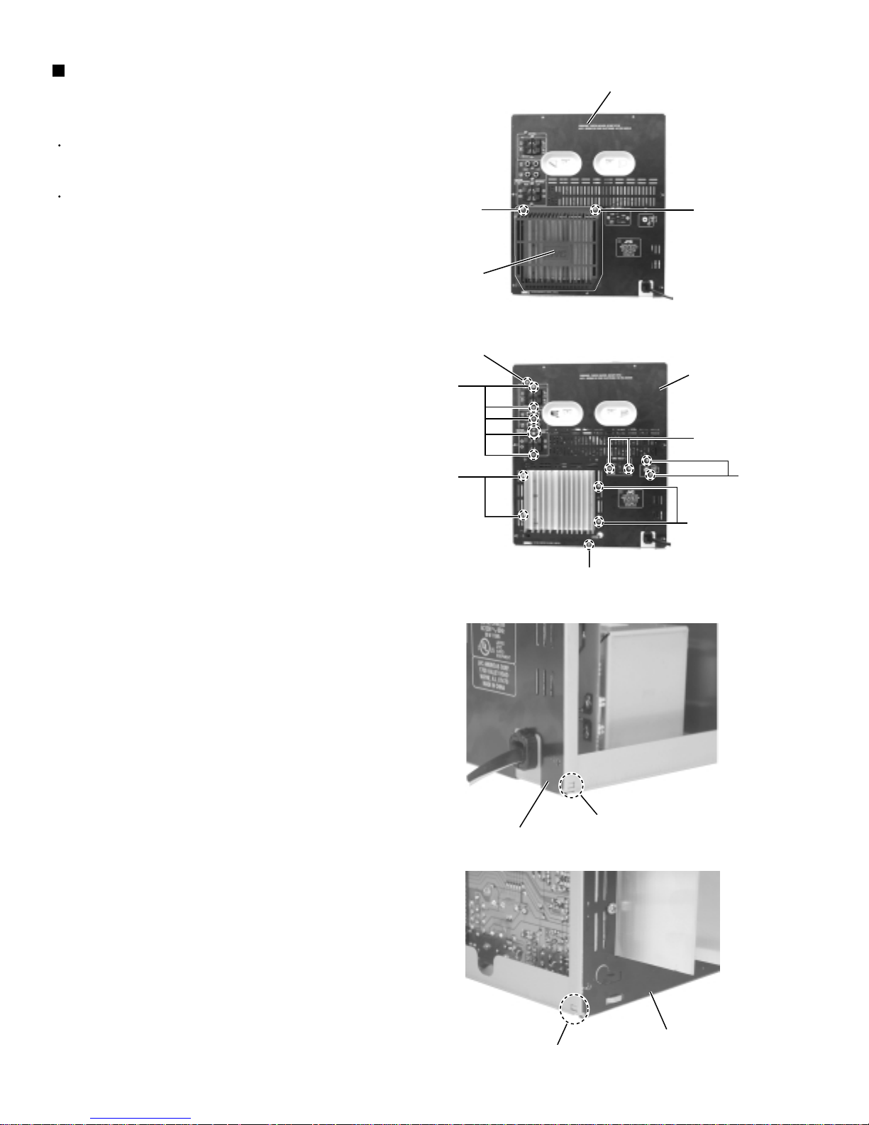
MX-J270V
Prior to performing the following procedures, remove
the metal cover, the CD changer mechanism
assembly, the rear cover, the rear panel, the voltage
selector and the video board.
It is not necessary to remove the front panel
assembly.
Disconnect the card wires from connector CN302,
CN306, CN307 and the harnesses from CN301,
CN305, CN901A and CN901B on the inside of the
main board.
Disconnect the harness from CN312 on the video
board.
From the right side of the body, remove the screw M
attaching the main board to the chassis base.
1.
2.
3.
Removing the main board
(See Fig.16 to 19)
Prior to performing the following procedure, remove
the rear cover, rear panel, voltage selector and the
video board.
Remove the two screws N attaching the heat sink to
the main board. Remove the IC bracket 1 and 2 on
the back of the heat sink.
Pull out the heat sink toward you.
1.
2.
~To remove the heat sink from
the main board~
Prior to performing the following procedures, remove
the main board.
Release the two joints h and i using a screwdriver
and detach the DSP board toward you.
1.
Removing the DSP board
(See Fig.19)
Fig.16
Fig.17
M
Main board
Main board
CN306
CN307
CN302
CN305
CN301
CN901A,CN901B
Fig.18
Heat sink
N
Main board
Fig.19
Heat sink
IC bracket 2
IC bracket 1
CN312
DSP board
DSP board
Joint i
Joint h
DSP board
Video board
1-9
Page 10
MX-J270V
Removing the power transformer
assembly
(See Fig.20 to 22)
Prior to performing the following procedure, remove
the metal cover, the CD changer mechanism
assembly and the voltage selector.
1.
Disconnect the harness from connector CN901A and
CN901B on the inside of the main board.
2.
Cut off the tie band j of the power transformer
assembly and unsolder the power cord.
(Make sure to bundle the wires after repair.)
3.
Remove the four screws O attaching the power
transformer assembly.
When removing the power transformer assembly
with the power cord, remove the rear panel and pull
out the power cord stopper from the bottom chassis
upward.
CN901A,CN901B
Video board
Voltage selector board
Power transformer assembly
Fig.20
O
Voltage selector board
Front panel
assembly
Voltage selector board
Video board
Tie band j
Rear panel
Power cord stopper
O
Power transformer
Fig.21
Power transformer
assembly
Fig.22
assembly
1-10
Page 11
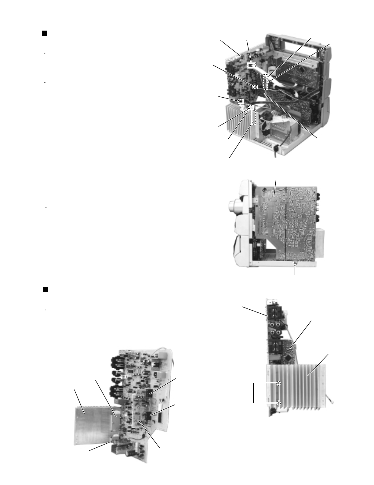
MX-J270V
<Front panel assembly>
Removing the MIC/headphone board
(See Fig.23 and 24)
Prior to performing the following procedure, remove
the metal cover, the CD changer mechanism
assembly and the front panel assembly.
1.
Remove the two screws P attaching the MIC
/headphone board.
2.
Pull out the MIC LEVEL knob from front side.
Removing the cassette mechanism
assembly
(See Fig.25)
Prior to performing the following procedure, remove
the metal cover, the CD changer mechanism
assembly and the front panel assembly.
1.
Disconnect the card wire from connector CN305 on
the cassette amplifier board.
2.
Remove the eight screws Q attaching the cassette
mechanism assembly.
3.
Detach the cassette mechanism assembly toward
you.
Removing the cassette amplifier board
(See Fig.26)
Fig.23
Cassette
mechanism
assembly
Q
MIC/headphone board
Front panel assembly
P
MIC LEVEL knob
Fig.24
Front panel assembly
CN305
Q
Q
Prior to performing the following procedure, remove
the cassette mechanism assembly.
1.
Disconnect the card wire from connector CN301 and
CN302 on the cassette amplifier board.
2.
Remove the six screws R attaching the cassette
amplifier board.
3.
Unsolder the soldering k on the harness for the DC
motor.
4.
Detach the cassette amplifier board toward you.
Q
Cassette amplifier board
DC motor
R
Soldering k
CN302
R
Q
R
Q
Fig.25
Fig.26
Cassette amplifier
board
Cassette mechanism
board
R
CN301
R
R
1-11
Page 12
MX-J270V
Removing the display board and the
bracket (See Fig.27 and 28)
Prior to performing the following procedure, remove
the metal cover, the CD changer mechanism
assembly and the front panel assembly.
Disconnect the card wire from connector CN306 on
1.
the cassette amplifier board.
Remove the four screws S attaching the front panel
2.
assembly.
Remove the four screws T attaching the front panel
3.
assembly.
Unsolder FW701, FW702, FW703, FW704 and
4.
FW705 on the display board. Disconnect the
harnesses extending from the power switch board,
the eject switch board, the volume board and the
multi-control board respectively
Removing each board in the front panel
assembly (See Fig.29 to 31)
Prior to performing the following procedure, remove
the display board.
~Removing the multi-control board~
(See Fig.29)
1.
Remove the eight screws U attaching the multicontrol board.
~Removing the volume board~
(See Fig.30 and 31)
1.
Pull out the volume knob on the front side of the front
panel assembly and remove the nut attaching the
volume board.
2.
Unhook the two hooks l on the back of the front
panel assembly and detach the volume board.
~Removing the eject switch board ~
(See Fig.29)
Remove the four screws V attaching the eject switch
1.
board.
~Removing the power switch board~
(See Fig.29)
Remove the three screws W attaching the power
1.
switch board.
Front panel
assembly
Bracket
Display board
FW703
FW701
T
Display board
Eject
switch
board
Volume
board
U
U
V
T
S
Fig.27
Fig.28
U
Front panel assembly
Front panel assembly
FW702
T
FW704
FW705
W
Power
switch
board
Multi-
control
board
U
U
Volume
knob
Volume
Fig.30
1-12
board
Fig.31
Hooks l
Front panel assembly
U
Fig.29
Page 13
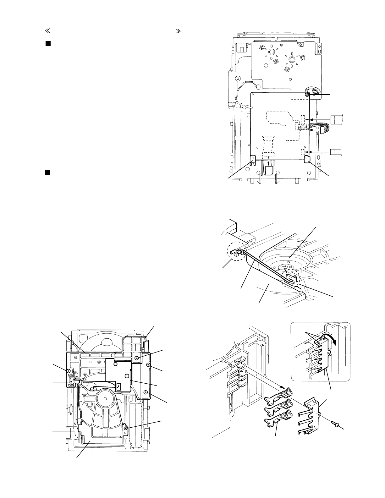
CD Traverse Mechanism Type:C3CN Section
Removing the CD Servo control board
(See Fig.1)
1.
Remove the Metal cover.
2.
Remove the CD Traverse mechanism assembly.
3.
From bottom side the CD Traverse mechanism
assembly, remove the one screw A retaining the CD
Servo control board.
From the connectors CN601, CN603, CN604 on the CD
4.
Servo control board, disconnect the card wire, from the
connector CN602, disconnect the six pin connector
wire.
Disengage the two engagements "a" , remove the CD
5.
Servo control board.
Removing the CD tray assembly
(See Fig.2~4)
Remove the front panel assembly.
1.
Remove the CD Traverse mechanism assembly.
2.
Remove the CD Servo control board.
3.
Remove the screw B retaining the disc stopper
4.
(See Fig.3).
Remove the three screws C retaining the T.bracket
5.
(See Fig.3).
From the clamper base section "c" , remove both of the
6.
edges fixing the rod(See Fig.2 and 3).
Remove the screw D retaining the clamper assembly
7.
(See Fig.3).
From the left side face of the chassis assembly, remove
8.
the one screw E retaining both of the return spring and
lock lever(See Fig. 4).
By removing the pawl at the section "d" fixing the return
9.
spring, dismount the return spring(See Fig.4).
Remove the three lock levers(See Fig.4).
10.
Disc stopper
T.Braket
MX-J270V
A
CD servo control board
CN604
CN
602
CN603
CN601
a
a
Fig.1
Clamper base
b
Rod
c
T.Braket
Fig.2
d
C
b
c
Clamper ass'y
Fig.3
B
C
Lod stopper
(C/J version only)
Return spring
C
D
E
Lock lever
Fig.4
1-13
Page 14
MX-J270V
11.
Check whether the lifter unit stopper has been caught
into the hole at the section "e" of CD tray assembly as
shown in Fig.5.
Make sure that the driver unit elevator is positioned as
12.
shown in Fig.6 from to the second or fifth hole on the
left side face of the CD Traverse mechanism assembly.
[Caution]
13.
14.
15.
Chassis assembly
In case the driver unit elevator is not at above
position, set the elevator to the position as
shown in Fig.7 by manually turning the pulley
gear as shown in Fig.8.
Manually turn the motor pulley in the clockwise
direction until the lifter unit stopper is lowered from the
section "e" of CD tray assembly(See Fig.8).
Pull out all of the three stages of CD tray assembly in
the arrow direction "f" until these stages stop
(See Fig.6).
At the position where the CD tray assembly has
stoppend, pull out the CD tray assembly while
pressing the two pawls "g and g' "on the back side of
CD tray assembly(See Fig.9). In this case, it is easy to
pull out the assembly when it is pulled out first from the
stage CD tray assembly.
Stopper
e
CD tray
assembly
Fig.5
Refer to Fig.7
Pulley gear
Pawl
CD tray assembly
g
f
Drive unit of elevator
Fig.7Fig.6
CD tray assembly
Motor pulley
Fig.8
1-14
Pawl ,
g
Fig.9
g'
Page 15
MX-J270V
Removing the CD mechanism
assembly (See Fig.10)
1.2.While turning the cams R1 and R2 assembly in the
arrow direction "h", align the shaft "i" of the CD
mechanism assembly to the position shown in Fig.10.
Remove the four screw F retaining the CD mechanism
assembly.
Removing the CD mechanism
(See Fig.11 and 12 )
For dismounting only the CD mechanism without
1.
removing the CD mechanism assembly, align the shaft
"j" of the CD mechanism assembly to the position
shown Fig.11 while turning the cam R1 and R2
assembly in the arrow direction "k".
By raising the CD mechanism assembly in the arrow
2.
direction "l" , remove the assembly from the lifter unit
(See Fig.12).
Cam R1, R2 assembly
Cams R1, R2 assembly
Arrow
h
i
F
F
CD mechanism assembly
F
F
Fig.10
CD mechanism
j
Fig.11
Removing the CD pick unit
(See Fig.13 )
Move the cam gear in the arrow direction m . Then, the
1.
CD pickup unit will be moved in the arrow direction n .
According to the above step, shift the CD pickup unit to
2.
the center position.
While pressing the stopper retaining the shaft in the
3.
arrow direction o , pull out the shaft in the arrow
direction p .
After dismounting the shaft from the CD pickup unit,
4.
remove the CD pickup unit
Arrow
k
Lifter unit
o
Stopper
Shaft
Fig.12
CD Pickup unit
n
m
Shaft
p
Stopper
Fig.13
Arrow
CD mechanism
Shaft
Cam gear
l
1-15
Page 16
MX-J270V
Removing the actuator motor board
(See Fig.14, 15)
Absorb the four soldered positions "q" of the right and
1.
left motors with a soldering absorber(See Fig.14).
Remove the two screws G retaining the actuator motor
2.
board(See Fig.14).
Remove the two screws H retaining the tray select
3.
switch board(See Fig.15).
Removing the cam unit
(See Fig.15 to 18 )
1.
Remove the CD mechanism assembly.
2.
While turning the cam gear r, align the pawl "s" position
of the drive unit to the notch position(Fig.15) on the cam
gear r.
Pull out the drive unit and cylinder gear(See Fig.17).
3.
While turning the cam gear r, align the pawl "t" position
4.
of the select lever to the notch position(Fig.18) on the
cam gear r.
Remove the four screws I retaining the cam unit(cam
5.
gear r and cams R1/R2 assembly)(See Fig.18).
Motor L
G
Motor R
q
q
G
Actuator motor board
Fig.14
Chassis assembly
CN801
Fig.15
CN802
Drive unit
Tray select
switch board
Cylinder gear
CN804
Drive unit
s
H
Cam gear L
I
Cam gear r
Fig.16
I
Cams R1, R2 assembly
Cam unit
I
1-16
Fig.17
t
Select lever
Fig.18
Page 17
MX-J270V
Removing the actuator motor and belt
(See Fig.19 to 22)
1.
Remove the two screws J retaining the gear bracket
(See Fig.19).
2.
While pressing the pawl "u" fixing the gear bracket in
the arrow direction, remove the gear bracket
(See Fig.19).
From the notch "v section" on the chassis assembly
3.
fixing the edge of gear bracket, remove and take out the
gear bracket(See Fig. 20).
Remove the belts respectively from the right and left
4.
actuator motor pulleys and pulley gears(See Fig. 19).
After turning over the chassis assembly, remove the
5.
actuator motor while spreading the four pawls "w" fixing
the right and left actuator motors in the arrow
direction(See Fig. 21).
[Note]
When the chassis assembly is turned over under
the conditions wherein the gear bracket and belt
have been removed, then the pulley gear as well
as the gear, etc. constituting the gear unit can
possibly be separated to pieces. In such a case,
assemble these parts by referring to the assembly
and configuration diagram in Fig. 22.
Pully gear
Gear bracket
Belt
Motor pulley
J
Fig.19
Actuator motor
Pulley gear
Belt
Motor pulley
J
Pawl
u
Chassis assembly
v
Gear bracket
Fig.20
Assembly and Configuration Diagram
Pulley gear
w
w
Fig.21
Pulley gear
Gear B
Cylinder gear
Gear B
Gear C
Select gear
Gross gear L
Fig.22
Gross gear U
Gear C
1-17
Page 18

MX-J270V
Removing the cams R1/R2 assembly
and cam gear r (See Fig.23)
Remove the slit washer fixing the cams R1 and R2
1.
assembly.
By removing the two pawls "x" fixing the cam R1,
2.
separate R2 from R1.
Remove the slit washer fixing the cam gear r.
3.
Pull out the cam gear r from the C.G. base assembly.
4.
Slit washer
Cam gear r
Removing the C.G. base assembly
(See Fig.23 and 24)
Remove the three screws K retaining the C.G. base
assembly.
[Caution]
To retassemble the cylinder gear, etc.with the
cam unit (cam gear and cans R1/R2 assembly),
gear unit and drive unit, align the position of the
pawl "s" on the drive unit to that o f the notch
on the cam gear r. Then, make sure that the
gear unit is engaged by turning the cam gear r
(See Fig. 24).
K
Slit washer
Cam R2
Pawl
Cam R1
x
Cam switch board
C.G. base assembly
Pawl
x
Notch
Pawl
s
Cylinder
gear
Drive unit
Fig.23
Cam gear r
Cam R1, R2 assembly
Gear unit
Gear bracket
Fig.24
1-18
Page 19
MX-J270V
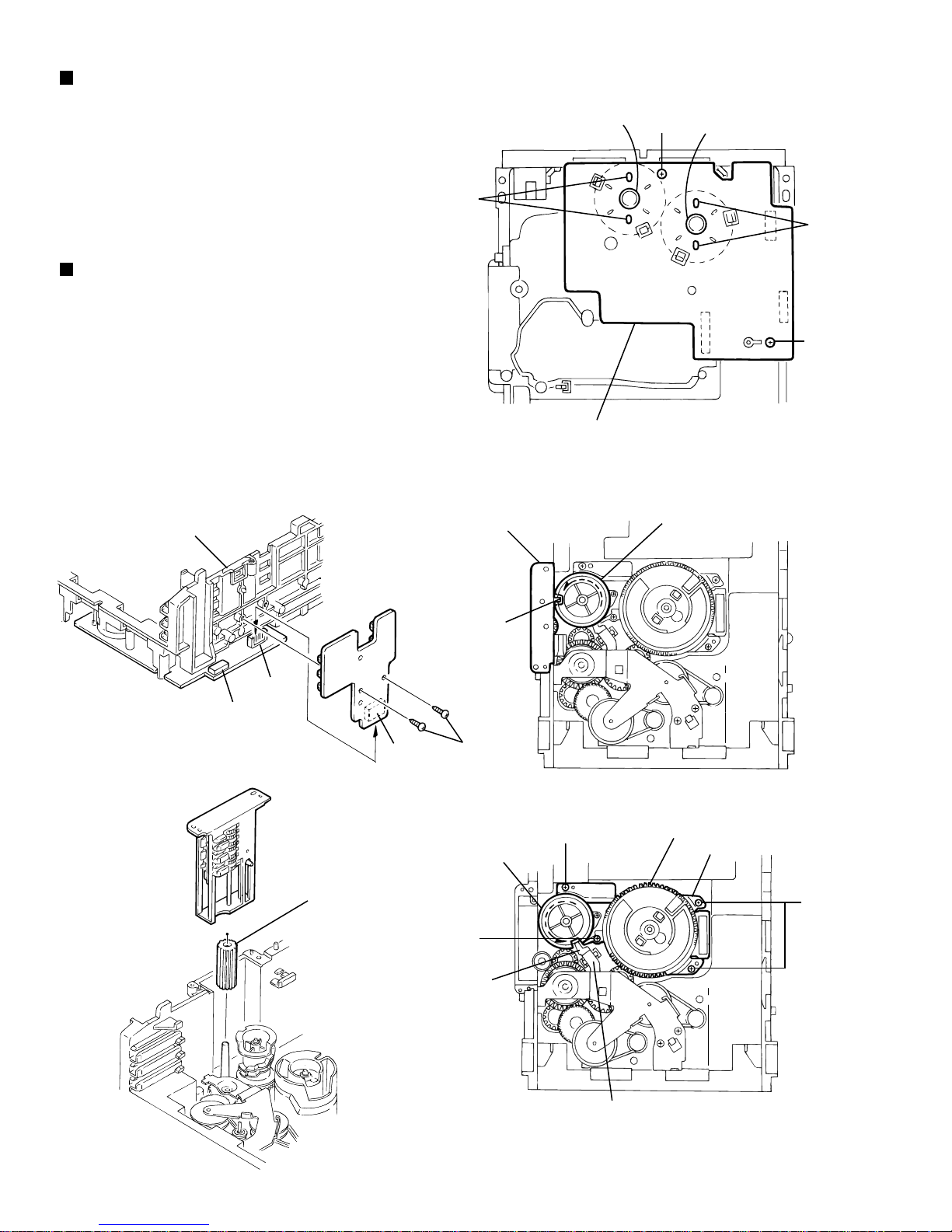
< Cassette mechanism section >
Removing the playback, recording and eraser
heads (See Fig.1~3)
1. While shifting the trigger arms seen on the right
side of the head mount in the arrow direction,turn
the flywheel R in counterclockwise direction until
the head mount has gone out with a click
(See Fig. 1).
2. When the flywheel R is rotated in counterclockwise
direction, the playback head will be turned in
counterclockwise direction from the position in
Fig.2 to that in Fig.3.
3. At this position, disconnect the flexible P.C.board
(outgoing from the playback head) from the
connector CN301 on the head amp. and mechanism
control P.C. board.
4. After dismounting the FPC holder,remove the
flexible P.C.board.
5. Remove the flexible P.C.board from the chassis
base.
6. Remove the spring "a" from behind the playback
head.
7. Loosen the reversing azimuth screw retaining the
playback head.
8. Take out the playback head from the front of the
head mount.
9. The recording and eraser heads should also be
removed similarly according to Steps 1~8 above.
Reassembling the playback, recording
and eraser heads (See Fig.2,3)
Cassette mechanism
Fig.1
Playback/Recording &
eraser head
Flexible
P.C.board
CN301
Head amplifier & mechanism
control P.C. board
Fig.2
Flywheel R
Trigger armHead mount
(Mechanism A side)
Spring "a"
Trigger arm
Flywheel R
(Mechanism A side)
1. Reassemble the playback head from the front of
the head mount to the position as shown in Fig.3.
2. Fix the reversing azimuth screw.
3. Set the spring a from behind the playback head.
4. Attach the flexible P.C.board to the chassis base,
and fix it with the FPC holder as shown in Fig.3.
5. The recording and eraser heads should also be
reassembled similarly according to Steps 1~4
above.
Playback head
Spring "a"
FPC holder
Fig.3
Reversing azimuth
screw
Head
mount
Flexible
P.C.board
CN302
Head amplifier &
mechanism control
P.C. board
(Mechanism B side)
1-19
Page 20

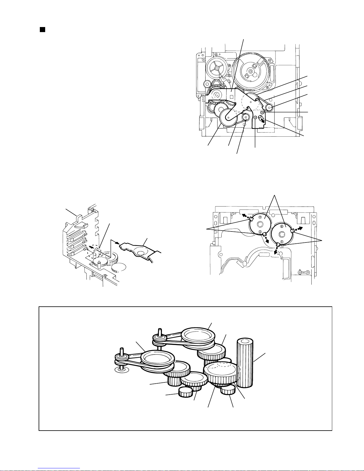
MX-J270V
Removing the head amp.and mechanism
control P.C.board (See Fig. 4)
1.Remove the cassette mechanism assembly.
2.After turning over the cassette mechanism
assembly, remove the five screws "A" retaining
the head amp. and mechanism control P.C.
board
3.Disconnect the connectors CN303 and CN304
on the P.C.Board and the connectors CN1 on
both the right and left side reel pulse
P.C.Boards.
4.When necessary, remove the 4pin parallel
wire soldered to the main motor
Removing the capstan motor assembly
1.Remove the six screws "B" retaining capstan
motor assembly (See Fig. 5).
2.While raising the capstan motor, remove the
capstan belts A and B respectively from the
motor pulley (See Fig. 6).
A
Flexible
board
Head amplifier &
mechanism control board
AA
CN304
CN302 CN301
Flexible
board
CN303
Fig.4
BB
Capstan motor
assembly
AA
Caution 1: Be sure to handle the capstan
belts so carefully that these belts
will not be stained by grease and
other foreign matter. Moreover,
these belts should be hand while
referring to the capstan belt
hanging method.
Capstan
belt A
BBBB
Fig.5
Capstan motor
Capstan
belt B
Capstan
belt A
Fig.7 Fig.6
1-20
Capstan
belt B
Motor pulley
Page 21

MX-J270V
Removing the capstan motor (See Fig. 8)
From the joint bracket, remove the two screws "C"
retaining the capstan motor.
Removing the flywheel (See Fig. 9,10)
1.Remove the head amp. and mechanism control
P.C.Board.
2.Remove the capstan motor assembly.
3.After turning over the cassette mechanism, remove
the slit washers "a" and "b" fixing the capstan shafts
R and L, and pull out the flywheels R and L respectively
from behind the cassette mechanism.
Removing the reel pulse P.C.board and solenoid
(See Fig. 11)
1.Remove the five pawls (c,d,e,f,g) retaining
the reel pulse P.C.Board.
2.From the surface of the reel pulse P.C.Board parts,
remove the two pawls "h" and "i" retaining the solenoid.
Capstan motor
Joint
bracket
Flywheel R Flywheel L
Flywheel R Flywheel L
Slit
washer "a"
Slit
washer "b"
Reel pulse board
Solenoid
Solenoid
C
C
a
b
c
d
e
f
g
hi
Fig.8
Fig.9
Fig.11
Fig.10
1-21
Page 22

MX-J270V
Adjustment method
Measuring devices necessary for
adjustment
1. Low-frequency oscillator
It must have the ability to output 600ohm from 0
dBs at an oscillation frequency of 20 Hz - 50 Hz.
2. Attenuator impedance: 600ohm
3. Electronic voltmeter
4. Distortion meter
5. Frequency counter
6. Wow and flutter meter
7. Test tapes
VT-712: tape speed and rotational distortion (3 kHz)
VT-724: standard level (1 kHz)
VT-703: head angle adjustment (10 kHz),
or use VT-73
VT-739: reproduction of frequency characteristics
(1 kHz, 63 Hz, 10 kHz)
Tuner section
Voltage input to the tuner ..................... +B: DC 5.7 V
VT: DC 12 V
Standard measuring output ..26.1 mV (0.28 V) /3ohm
Input locations ................ AM: standard loop antenna
FM: TP1 (hot) and TP2 (GND)
Standard settings for measuring
volume
Sound ................................................................. OFF
Effective hyper bass ........................................... OFF
Volume adjustment ...................................... VOL. 23
Precautions for measuring
1. Input 30 pF and 33 kohm to the IF sweeper output
and 0.082 F and 100 kohm to the sweeper input,
respectively.
2. Lower the output level of the IF sweeper as much
as possible in the adjustable range.
8. Blank tape
Type I : AC-225 (TDK-AD)
Type II : AC-514 (TDK-SA)
9. Torque gauge: Tension gauge for playback,
fast-forward and rewind.
FWD (TW211A), REW (TW212A)
and FF/REW (TW2231A)
Specifications for measurement
Power supply voltage .......AC 110 to 240 V (50/60 Hz)
Standard output .....................Speaker: 0.775 V/6ohm
Headphone:0.245V/32ohm
Standard frequency and input level
................ 1 kHz: AUX: -8 dBs
Input level for reproduction of recording characteristics
................... AUX: -28 dBs
Measuring output terminal ................. Speaker: JA303
Load resistance .................................................. 6ohm
Radio input signal
AM frequency ................................................... 400 Hz
Degree of modulation in AM band ....................... 30%
FM frequency ................................................... 400 Hz
Frequency deviation in FM band ................... 22.5 kHz
3. The IF sweeper needs no adjustment as it is a
fixed component.
4. It is not necessary to perform any kind of
adjustment on the MPX, as a ceramic oscillator is
used for measuring.
5. FM tracking adjustment is not necessary as a fixed
coil is used.
6. The grounding circuit is separate from the input
and output. Therefore, be sure to connect to ground
carefully when measuring both the input and output
voltages simultaneously using 2 channels of the
electronic voltmeter.
7. The speaker's minus terminal cannot be connected
to ground when using a BTL format amplifier.
Therefore, do not connect any type of ground wire
to this terminal. The OTL format is used with this
system.
8. Use a large wire to connect to the dummy
impedance generator when measuring the output.
9. Be sure to use a band pass filter (DV-12) when
using mixed tape.
1-22
Page 23

Arrangement of Adjusting Positions
MX-J270V
Cassette mechanism section (Mechanism A section)
Head azimuth
adjusting screw
(Forward side)
Playback
head
Head azimuth
adjusting screw
(Reverse side)
Cassette mechanism section (Back side)
Head azimuth
adjusting screw
(Forward side)
Playback,recording and eraser
heads or playback head
Head azimuth
adjusting screw
(Reverse side)
Cassette Mechanism Unit Section
Head amplifier
mechanism control board
Tape speed ADJ
Bias ADJ L
Bias ADJ R
1-23
Page 24

MX-J270V
Tape Recorder Section
Items Measurement
Confirmation
of head angle
conditions
Test tape
:VT703(10kHz)
Measurement
output terminal
:Speaker terminal
Speaker R
(Load resistor:3ohm)
:Headphone terminal
Measurement method
1.Playback the test tape VT703(10kHz).
2.With the playback mechanism or recording &
playback mechanism, adjust the head azimuth
screw so that the forward and reverse output
levels become maximum.After adjustment,lock
the head azimuth at least by half a turn.
3.In either case,this adjustment should be
performed in both the forward and reverse
directions with the head azimuth screw.
Standard
values
Maximum
output
Adjusting
positions
Adjust the head
azimuth screw
only when the
head has been
changed.
Confirmation
of tape speed
Test tape
:VT712(3kHz)
Measurement
output terminal
:Headphone terminal
<Constant speed>
Adjust VR301 so that the frequency counter reading
becomes 3,000Hz 60Hz when playing back the
test tape VT712(3kHz)with the playback mechanism
or playback and recording mechanism after ending
forward winding of the tape.
Reference Values for Confirmation items
Items Measurement
Double tape
speed
Difference
between the
forward and
reverse speed.
P.mecha and
R/P mecha
speed
conditions
Test tape
:VT712(3kHz)
Measurement
output terminal
:Speaker terminal
Speaker R
(Load resistance
:3ohm)
measurement
output terminal
:Headphone terminal
After setting to the double speed motor, confirm
that the frequency counter reading becomes
4,800+400/-300Hz when the test tape VT712
(3kHz) has been play back with the playback
mechanism.
When the test tape VT712(3kHz) has been played
back with the playback mechanism or recording and
playback mechanism at the beginning of forward
winding, the frequency counter reading of the
difference between both of the mechanisms should
be 6.0Hz or less.
Measurement method
Tape speed
of decks
(A and B)
:3,000Hz
60Hz
Standard
values
4,800+400/
-300Hz
60Hz or
less
VR301
Adjusting
positions
Playback
mechanism side
Both the playback
and recording &
playback
mechanism
Wow & flutter
Test tape
:VT712(3kHz)
Measurement
output terminal
:Headphone terminal
When the test tape VT712(3kHz) has been played
back with the playback mechanism or recording and
playback mechanism at the beginning of forward
winding the frequency counter reading of wow &
flutter should be 0.25% or less(WRMS).
1-24
with in
0.25%
JIS(WTD)
Both the playback
and recording &
playback
mechanism
Page 25

Electrical Performance
Items Measurement
Adjustment of
recording bias
current
(Reference
value)
conditions
*Mode : Forward or
reverse mode
*Recording mode
*Test tape
:AC-514 and AC-225
Measurement output
terminal
:Both recording and
headphone terminals
Measurement method
1.With the recording and playback mechanism,
load the test tapes(AC-514 to TYP and AC-225 to
TYP ),and set the mechanism to the recording and
pausing conditions in advance.
2.After connecting 100ohm in series to the recorder
head,measure the bias current with a valve
voltmeter at both of the terminals.
3.After resetting the [PAUSE] mode,start recording.
At this time,adjust VR101 for LcH and VR201 for
RcH so that the recording bias current values
become 4.0 A (TYP ) and 4.20 A(TYP ).
Standard
values
AC-225
:4.20 A
AC-514
:4.0 A
MX-J270V
Adjusting
positions
LcH
:VR101
RcH
:VR201
Adjustment of
recording and
playback
frequency
characteristics
Reference frequency
:1kHz and 10kHz
(REF:-20dB)
Test tape
:TYP AC-514
Measurement input
terminal
:OSC IN
1.With the recording and playback mechanism,load
the test tape(AC-514 to TYP ),and set the
mechanism to the recording and pausing condition
in advance.
2.While repetitively inputting the reference frequency
signal of 1kHz and 10kHz from OSC IN, record and
playback the test tape.
3.While recording and playing back the test tape in
TYP ,adjust VR101 for LcH and VR201 for RcH
so that the output deviation between 1kHz and
10kHz becomes -1dB 2dB.
Reference Values for Electrical Function Confirmation Items
Items Measurement
Recording
bias frequency
conditions
*Recording and
playback side forward
or reverse
*Test tape
:TYP AC-514
*Measurement
terminal BIAS TP on
P.C.board
1.While changing over to and from BIAS 1 and 2,
confirm that the frequency is changed.
2.With the recording and playback mechanism.
load the test tape (AC-514 to TYP ),and set the
mechanism to the recording and pausing
conditions in advance.
3.Confirm that the BIAS TP frequency on the
P.C.board is 100kHz 6kHz.
Measurement method
Output
deviation
between
1kHz and
10kH
:-1dB 2dB
Standard
values
100kHz
+9kHz
-7kHz
LcH
:VR101
RcH
:VR201
Adjusting
positions
Eraser current
(Reference
value)
*Recording and
playback side forward
or reverse
*Recording mode
*Test tape
:AC-514 and AC-225
Measurement terminal
Both of the eraser
head
1.With the recording and playback mechanism,
load the test tapes(AC-514 to TYP and AC-225
to TYP ),and set the mechanism to the recording
and pausing condition in advance.
2.After setting to the recording conditions,connect
1Mohm in series to the eraser head on the recording
and playback mechanism side,and measure the
eraser current from both of the eraser terminal.
TYP
:120mA
TYP
:75mA
1-25
Page 26

MX-J270V
Flow of functional operation until TOC read
Power ON
Power Key
Slider turns REST
SW ON.
Automatic tuning
of TE offset
Check Point
Check that the voltage at the pin 5
of CN602 is 0V (a moment)?
VREF
Tracking error waveform at TOC reading
pin 25 of
IC601(TE)
Approx
1.8V
Tracking
servo
Disc statas
to rotate
off statas
Automatic measurement
of TE amplitude and
automatic tuning of
TE balance
Approx.3sec
Tracking
servo
on statas
Disc to be
braked to stop
TOC reading
finishes
500mv/div
2ms/div
Fig.1
Laser ON
Detection of disc
Automatic tuning of
Foucus offset
Automatic measurement of
Focus A-curve amplitude
Disc is rotated
Focus servo ON
(Tracking servo ON)
Automatic measurement of
Tracking error amplitude
Automatic tuning of
Tracking error balance
Check that the voltage at the
pin3 of IC601 + side is + 5V?
Confirm that the Focus error
S-cuve siganl at the pin27 of
IC601 is approx.2Vp-p
Confirm that the siganl from
pin24 IC603 is 0V as a
accelerated pulse during
approx.400ms.
Confirm the waveform of
the Tracking error signal
at the pin25 of IC601 (R612)
(See fig-1)
1-26
Automatic tuning of
Focus error balance
Automatic tuning of
Focus error gain
Automatic tuning of
Tracking error gain
TOC reading
Play a disc
Confirm the eys-pattern
at the lead of TP602
Page 27

MX-J270V
Maintenance of laser pickup
(1) Cleaning the pick up lens
Before you replace the pick up, please try to
clean the lens with a alcohol soaked cotton
swab.
(2) Life of the laser diode (Fig.1)
When the life of the laser diode has expired,
the following symptoms wil appear.
(1) The level of RF output (EFM output:ampli
tude of eye pattern) will below.
Is RF output
1.1 0.15Vp-p?
YES
O.K
NO
Replace it.
Replacement of laser pickup
Turn off the power switch and,disconnect the
power cord from the ac outlet.
Replace the pickup with a normal one.(Refer
to "Pickup Removal" on the previous page)
Plug the power cord in,and turn the power on.
At this time,check that the laser emits for
about 3seconds and the objective lens moves
up and down.
Note: Do not observe the laser beam directly.
Play a disc.
(Fig.1)
(3) Semi-fixed resistor on the APC PC board
The semi-fixed resistor on the APC printed
circuit board which is attached to the pickup
is used to adjust the laser power.Since this
adjustment should be performed to match the
characteristics of the whole optical block,
do not touch the semi-fixed resistor.
If the laser power is lower than the specified
value,the laser diode is almost worn out, and
the laser pickup should be replaced.
If the semi-fixed resistor is adjusted while
the pickup is functioning normally,the laser
pickup may be damaged due to excessive current.
Check the eye-pattern at TP1.
Finish.
1-27
Page 28

MX-J270V
Description of major ICs
AN8806SB (IC601) : RF&Servo AMP
1.Pin layout
PD
LD
LDON
LDP
VCC
RF-
RF OUT
RF IN
C.AGC
ARF
C.ENV
C.EA
CS BDO
BDO
CS BRT
OFTR
/RFDET
GND
1
2
3
4
5
6
7
8
9
10
11
12
13
14
15
16
17
18
36
35
34
33
32
31
30
29
28
27
26
25
24
23
22
21
20
19
PDAC
PDBD
PDF
PDE
PDER
PDFR
TBAL
FBAL
FE FE OUT
TE TE OUT
CROSS
TE BPF
VDET
LD OFF
VREF
ENV
2.Block diagram
36
--
+
35
-+
31
34
-+
32
33
-+
6
--
VCBA
+
29
728
-+
--
+
+
VCBA
--
+
VCBA
--
--
VCBA
+
+
--
-+
-+
+
--
27
-+
--
EQ
+
+
--
+
--
910 17
8
AGC
OFTR
BDO
RF
DET
11
12 19
ENV CURCUIT
13
14
15
16
-+
20
21
2
24 25
30
1-28
23
26
22
14
3
Page 29

35
36
34
33
32
31
30
29
28
27
26
25
24
23
22
21
20
19
18
17
16
15
14
13
12
11
10
9
8
7
6
5
4
3
2
1
3. Pin function
PD AC
FBAL
TBAL
PDFR
PDER
PDE
PDF
PD BD
TE BPF
VDET
CROSS
TE OUT
TE-
FE OUT
FE-
/RFDET
GND
LD OFF
VREF
ENV
OFTR
C.AGC
ARF
C.ENV
C.EA
CS BDO
BDO
CS BRT
LD
LD ON
LDP
VCC
RF-
RF OUT
RF IN
PD
Pin No.
Symbol
I/O
I
O
I
--
-I
O
I
I/O
O
I/O
I/O
I/O
O
I/O
O
O
-O
O
-O
I
O
O
I
O
I
I
I
I/O
I/O
I
I
I
I I-V amp input
I-V amp input
I-V amp input
I-V amp input
E I-V amp gain control
F I-V amp gain control
Tracking balance control
Focus balance control
Inverse input pin for focus error amp
Output pin of focus error
Inverse input pin for tracking error amp
Tracking error signal output
Tracking error cross output
Input pin of tracking error through BPF
Vibration detection signal output
Connect to ground
Reference voltage output
Description
APC amp input terminal
APC amp output terminal
APC ON/OFF control terminal
Envelope output
Ground
RF detection signal output
Of-track status signal output
BDO output pin
A capacitor is connected to this terminal to detect the envelope of RF signal
RF output
Connecting pin of AGC loop filter
RF input
RFamp output
Inverse input pin for RF amp
Power supply
Connect to ground
A capacitor is connected to this terminal to detect the envelope of RF signal
A capacitor is connected to detect the lower envelope of RF signal
A capacitor is connected to detect the lower envelope of RF signal
MX-J270V
1-29
Page 30

MX-J270V
BA15218F (IC852) : OP AMP.
1OUT1
2-IN1
-
8
7
CC
V
OUT2
1
3+IN1
+
-
-IN2
6
2
4
+
+IN2
5GND
BA15218N (IC301,303,305,307) : Dual Ope. Amp.
+
+
1
-
1 2 3 4 5 6 7 8
OUT1 +IN1 +IN1
+IN2 -IN2 OUT2
GND
2
-
Vcc
TA8409S (IC851,852) : Motor driver
1.Pin layout 2.Pin function
1
IN2
VCC
OUT 2
NC
GND
VS
OUT 1
VREF
IN1
2
3
4
5
6
7
8
9
TA8409S
INPUT OUTPUT MODE
IN1
IN2
0
0
1
0
0
1
1
1
TC7SH04FU (IC108) : CMOS Inverter
NC
IN A
1
2
5
VCC
OUT1
H
L
L
OUT2
L
H
L
MOTOR
STOP
CW/CCW
CCW/CW
BRAKE
GND
3
4
OUT Y
1-30
Page 31

BA6897FP (IC801) : 4channel driver
MX-J270V
CH1-OUTA
CH1-OUTB
CH1-INA
CH1-INB
TEST1
TEST2
MUTE
GND
CH2-INB
CH2-INA
CH2-OUTB
CH2-OUTA
GND
D.BUF
1
2
D.BUF
3
4
5
6
7
8
9
10
D.BUF
11
12
D.BUF
13
- +
Level
shift
Level
shift
- +
+ Level
shift
T.S.D
DRIVER
MUTE
+-
-+
Level
shift
+ -
-+
+-
D.BUF
D.BUF
-+
D.BUF
D.BUF
28
27
26
25
24
23
22
21
20
19
18
17
16
GND
CH4-OUTA
CH4-OUTB
CH4-INA
CH4-INB
BIAS IN
Vcc
Vcc
CH3-INB
CH3-INA
CH3-OUTB
CH3-OUTA
OP IN(+)
OP-OUT
14
-+
15
OP IN(-)
1-31
Page 32

MX-J270V
BH3854 (IC306) : E.Volume
1.Terminal layout
2.Block diagram
IN2
RIP
32 31 30 29 28 27 26 25 24 23 22 21 20 19 18 17
NF2
32 17
116
TC
BVN2
BIN2
BVO2
2K
TIN2
TVO2
OUT2
10K
VC
10K
10K
BC
CLK
DATA
LATCH
VREF
( BASS ) (TREBLE)
TONE CONTROL
20K
Vcc
20K
20K
47K
47K
20K
VOLUME
MATRIX SURROUND SOUND
VOLUME
VOLUME
3.8V
CONTROL
Ref.Voltage
VOLUME
TONE CONTROL
( BASS )
1 2 3 4 5 6 7 8 9 10 11 12 13 14 15 16
IN1
A-GND
NF1
BVN1
BIN1
(TREBLE)
20K
BV01
TIN1
TVO1
Vcc
OUT1
Vcc
200K
SC
PORT1
PORT2
PORT3
PORT4
VSS
Volume, bass treble and surround can be also controlled externally by giving DC voltage
through VC (volume control) terminal, BC (bass control) terminal, TC (treble control)
terminal and SC (surround control) terminal.
Impedance of VC, TC and BC terminals is 10 K (Typ.).
Impedance of SC terminal is 200K (Typ.).
1-32
Page 33

MX-J270V
PIN PIN Name Function PIN PIN Name Function
1
2
3
4
5
6
7
8
9
10
11
12
13
14
15
16
A-GND
IN1
NF1
BVN1
BIN1
BV01
TIN1
TV01
OUT1
Vcc
SC
PORT1
PORT2
PORT3
PORT4
VSS
Analog system ground
Terminal for 1ch volume
input
Terminal for gain adjustment
of input step AMP
Terminal for connection of
1ch low-frequency filter
Terminal for connection of
1ch low-frequency filter
Terminal for connection of
1ch low-frequency filter
Terminal for connection of
1ch high-frequency filter
Terminal for connection of
1ch high-frequency filter
Terminal for 1ch volume
output
Terminal for power supply
Terminal for time constant
attachment for switching
shock protection
Terminal for port output
Terminal for port output
Terminal for port output
Terminal for port output
Digital system ground
17
18
19
20
21
22
23
24
25
26
27
28
29
30
31
32
VREF
LATCH
DATA
CLK
BC
TC
VC
OUT2
TV02
TIN2
BV02
BIN2
BVN2
NF2
IN2
RIP
Terminal for 3.8V reference
voltage output
Terminal to receive latch data
Terminal to receive data
Terminal to receive clock
Terminal for time constant
attachment for switching
shock protection
Terminal for time constant
attachment for switching
shock protection
Terminal for time constant
attachment for switching
shock protection
Terminal for 2ch volume
output
Terminal for connection of
2ch high-frequency filter
Terminal for connection of
2ch high-frequency filter
Terminal for connection of
2ch low-frequency filter
Terminal for connection of
2ch low-frequency filter
Terminal for connection of
2ch low-frequency filter
Terminal for gain adjustment
of input step AMP
Terminal for 2ch volume
output
Terminal for filter
BH3854
3. Pin function
1-33
Page 34

MX-J270V
BU2173F (IC105) : VCO
1.Terminal Layout 2.Block diagrams
VDD
TSTO
XTALI
XTALO
CTRLA
CTRLB
CTRLC
TSTI
VSS
1
2
3
4
5
6
7
8
9
18
17
16
15
14
13
12
11
10
3.Pin function
Pin No.
1
2
3
4
5
6
7
8
9
10
11
12
13
14
15
16
17
18
AVDD
FPUT4
VDDIO
FOUT1
TEST
FOUT2
VSSIO
FOUT3
AVSS
Symbol I/O Function
VDD
TSTO
XTALI
XTALO
CTRLA
CTRLB
CTRLC
TSTI
VSS
AVSS
FOUT3
VSSIO
FOUT2
TEST
FOUT1
VDDIO
FOUT4
AVDD
-
Digital VDD .
Use open this pin for normal operation.
I
Reference oscillation input.
O
Reference oscillation output.
Frequency select for V-CD/CD-G.
Force H for normal operation.
PAL/NTSC select for CD-G mode.
Force L for normal operation.
-
Digital GND.
-
Analog GND.
Use open this pin for normal operation.
-
I/O GND.
O
Clock output (2).
Force L for normal operation.
O
Clock output (1).
-
I/O VDD .
O
Clock output (4).
-
Analog VDD .
1-34
Page 35

1
2
3
4
5
6
7
8,9
10
11 15
16
17
18
19
20
21
22
23 28
29
30,31
32,33
34 37
38
39 42
43
44
45
46
47
48
49
50
51,52
53 57
58
59 63
64
65
66 72
73
74 76
77
78 80
81
82 84
85
86 89
90
91 94
95
96
97
98
99
100
101
102
103
104
105
106
107
108
109
110
111
112
113
114
115
116
117
118
119
120
121
122
123
124
125
126
127
128
HA2
DS
W/R
IRQ
DTACK
HD0
IO VDD
HD1,2
CKT VSS
HD3 7
IOVSS
TEST
XTLVSS
XTLIN
XTLOUT
XTLVDD
CKTVDD
MD0 5
IOVDD
MD6,7
MCE01
MD8 11
IOVSS
MD12 15
5VVDD
LCAS
LCASIN
CKTVSS
MWE
UCAS
IOVDD
UCASIN
RAS0,1
MA9 5
IOVSS
MA4 0
PIO0
IOVDD
VD0 6
IOVSS
VD7 9
CKTVDD
VD10 12
IOVDD
VD13 15
CKTVSS
VD16 19
IOVSS
VD20 23
VSYNC
HSYNC
VOE
VCOVDD
VCLK
VCOVSS
RESET
IOVSS
C2PO
CDLRCK
CDDATA
CDBCK
DALRCK
DADAT A
DABCK
IOVDD
XCK
CKTVDD
PIO12
PIO11
PIO10
PIO9
PIO8
PIO7
PIO6
PIO5
PIO4
PIO3
5VVDD
PIO2
IOVSS
PIO1
HA0
HA1
Host address.
Data strobe terminal.
I/O read terminal.
Interact terminal.
Acknowledge data output.
Host data terminal.
Power supply for input/output.
Host data terminal.
Connected to GND.
Date data terminal.
Ground terminal for Input/Output.
Test terminal.
Oscillator ground terminal.
Oscillator input terminal.
Oscillator output terminal.
Power supply for oscillator.
Power supply.
DRAM data / ROM data terminal.
Power supply for Input/Output.
DRAM data/ROM data terminal.
Chip enable output for ROM bank.
DRAM data/ROM data terminal.
Ground terminal for Input/Output.
DRAM data/ROM address terminal.
Power supply (+5V).
DRAM LCAS/ROM address terminal.
DRAM LCAS input.
Connect to GND.
DRAM write enable signal output.
DRAM UCAS/ROM address terminal.
Power supply for Input/Output.
DRAM UCAS input terminal.
DRAM RAS0,1 terminal.
DRAM data/ROM address terminal.
Ground terminal for Input/Output.
DRAM data/ROM address terminal.
ROM address extension terminal.
Power supply for Input/output.
Video data terminal
(R6/CrCb6/YCrCb066)
Ground terminal for Input/Output.
Video data terminal
(R7/CrCb7/YCrCb7)(G0,1/Y0,1)
Power supply.
Video data terminal (G24/Y24)
Power supply for Input/Output.
Video data terminal (G57/Y57)
Connect to GND.
Video data terminal(B0B3)
Ground terminal for Input/Output.
Video data terminal(B47)
Vertical comparator/Composite
comparator output.
Horizontal synchronizing signal.
Video output enable signal.
Power supply of VCO.
Video clock terminal.
Ground of VCO.
Reset signal input.
Ground terminal for Input/Output.
Data error flag input.
L/R word clock input.
Bit serial data input.
Bit clock output.
L/R clock output.
Bit serial PCM audio signal output.
Bit clock output.
Power supply for Input/Output.
Bit clock input terminal.
Power supply.
Interact 2 signal output.
Non connect.
Host enable signal input.
Boot ROM enable signal input.
Non connect.
DAC emphasis signal output.
CD-DA emphasis signal output.
Non connect.
FMV detect signal output.
CD-DA video CD select signal
output Low:Video CD.
Power supply (+5V).
Non connect.
Ground for Input/Output.
Non connect.
Host address input.
Host address input.
I
I
I
O
O
I/O
-
I/O
-
I/O
-
I
I
I
O
-
-
I/O
-
I/O
O
I/O
-
I/O
-
O
I
O
O
-
O
O
O
O
O
O
-
O
-
O
-
O
-
O
I/O
I/O
I
-
I/O
I
I
I
I
I
O
O
O
-
I
O
O
I
I
O
O
I
O
O
O
-
O
-
O
-
-
Pin No.
Symbol
I/O
Function
Pin No.
Symbol
I/O
Function
CL480-F1 (IC101) : MPEG-1 Audio / Video decoder
MX-J270V
1-35
Page 36

MX-J270V
HD74HCT244 (IC113) : Buffer
1. Terminal la yout
2. Block diagram
1-36
Page 37

1. Pin layout
1
2
3
4
5
6
7
8
9
10
11
22
21
20
19
18
17
16
15
14
13
12
XT
FM/AM
CE
DI
CLOCK
DO
FM/ST/VCO
AM/FM
SDIN
XT
GND
LPFIN
LPFOUT
PD
VCC
FMIN
AMIN
IFCONT
IFIN
Pin
No.
1
2
3
4
5
6
7
8
9
10
11
Pin
No.
12
13
14
15
16
17
18
19
20
21
22
Symbol
XT
FM/AM
CE
DI
CLOCK
DO
FM/ST/VCO
AM/FM
LW
MW
SDIN
Symbol
IFIN
IFCONT
AMIN
FMIN
VCC
PD
LPFOUT
LPFIN
GND
XT
Function
X'tal oscillator connect (75kHz)
LOW:FM mode
When data output/input for 4pin(input) and
6pin(output): H
Input for receive the serial data from
controller
Sync signal input use
Data output for Controller
Output port
"Low": MW mode
Open state after the power on reset
Input/output port
Input/output port
Data input/output
Function
IF counter signal input
IF signal output
Not use
AM Local OSC signal output
FM Local OSC signal input
Power suplly(VDD=4.5-5.5V)
When power ON:Reset circuit move
PLL charge pump output(H: Local OSC
frequency Height than Reference frequency.
L: Low Agreement: Height impedance)
Output for active lowpassfilter of PLL
Input for active lowpassfilter of PLL
Connected to GND
X'tal oscillator(75KHz)
I/O
I
O
I
I
I
O
O
O
I/O
I/O
I/O
I/O
I
O
-
I
I
-
O
O
I
I
Reference
Driver
Phase
Detector
Charge Pump
Unlock
Detector
Universal
Counter
Swallow Counter
1/16,1/17 4bit
12bit
Programmable
DriverS
Swallow Counter
1/16,1/17 4bit
Data Shift Register & Latch
Power
on
Reset
C
2B
I/F
1/2
782
11
13
21
17
6
5
4
3
15
16
22
1
18
19
20
12
2. Block diagram
3. Pin function
LC72136 (IC2) : PLL Frequency Synthesizer
MX-J270V
1-37
Page 38

MX-J270V
LH531HEG (IC102) : 1M ROM
1.Terminal Layout
VPP
A16
A15
A12
A7
A6
A5
A4
A3
A2
A1
A0
D0
D1
D2
GND
1
2
3
4
5
6
7
8
9
10
11
12
13
14
15
16
32
31
30
29
28
27
26
25
24
23
22
21
20
19
18
17
VCC
A18
A17
A14
A13
A8
A9
A11
CE
A10
CE
D7
D6
D5
D4
D3
2.Block diagram
2
A16
3
A15
29
A14
28
A13
4
A12
25
A11
23
A10
26
A9
27
A8
5
A7
6
A6
7
A5
8
A4
9
A3
10
A2
11
A1
12
A0
22
CE
BUFFER
ADDRESS/BUFFER
CE
ADDRESS/DECODER
TIMING
GENERATOR
MEMORY
MATRIX
(131,072 8bit)
CORAM
SELECTOR
SENS AMP.
3.Pin Function
Pin No.
1
2
3
4
5 12
13 15
16
17 21
22
23
24
25
26,27
28,29
30,31
A13,A14
D17,D18
32
Symbol
VPP
A16
A15
A12
A7A0
D0D2
GND
D3D7
CE
A10
CE
A11
A9,A8
VCC
I/O
I
I
I
I
O
-
O
I
I
I
I
I
I
O
-
OE
BUFFER
24
CE
Function
Power supply.
Adress input.
Adress input.
Adress input.
Adress input.
Data output.
Connect to GND
Data output.
Chip enable input.
Adress input.
Chip enable input.
Adress input.
Adress input.
Adress input.
Data output.
Power supply.
BUFFER
OUTPUT
32
16
GNDVCC
13 141517 18 19 20 21
D0 D1 D2 D3 D4 D5 D6 D7
1-38
Page 39

MN171601AK8J2 (IC111) : HOST Micro Computer
1.Terminal Layout
64 49
MX-J270V
1
16
17 32
2.Pin Function
Pin No.
1
2
3
4
5
6
7
8
9
10
11
12
13 15
16
17 24
25 39
40
41 48
49
50
51
52
53
54
55
56
57
58
59
60
61
62
63
64
Symbol
480RST
MREQ
ACTINT
GDET
GND
DTACK
GND
GND
DIR
N/PAL
RGB
W/R
HA02
DS
HD07
SA014
SCS
SD18
SR/W
PAL60
RESET
X1
X2
VSS
OSC2
OSC1
VDD
HREQ
SRCLK
M2HDT
M2MDT
HRDY
VCD/G
PALCDG
48
33
I/O Function
O
I/O
O
I/O
O
O
I/O
O
O
I/O
I/O
O
O
O
O
O
O
Reset signal output.
Input the transfer request data signal.
I
Interact 2 signal input.
I
CD-G detect terminal H:CD-G
I
Connected to GND.
Acknowledge signal input.
I
Connect to GND.
Connect to GND.
Input/Output control for IC114.
Not use.
Video out control signal (H:RGB L:composite)
Read/Write signal input/output.
Address signal output for MPEG LSI.
Data strobe signal output.
Data terminal for MPEG LSI.
SRAM address signal output.
SRAM chip select signal output.
SRAM data Input/Output terminal.
SRAM read/write signal input/output.
Not use.
Reset signal input.
I
Non connect
Non connect.
Connect to GND.
Non connect.
Clock input terminal.
I
Power supply.
Communication signal output.
Clock signal for data request.
Serial data output.
Serial data input.
I
Communication signal output.
Video swith switching signal output.
CD-G PAL/NTSC clock select terminal.
1-39
Page 40

MX-J270V
MN35510 (IC651) : Digital servo & digital signal processor
1. Terminal Layout
2.Block Diagram
LRCKIN(MSEL)
BCLK(SSEL)
SRDATAIN
(PSEL)
IOSEL
CLVS
CRC
BLKCK
CLDCK
SBCK
SUBC
DEMPH
RESY
FLAG6(RESY)
SSEL
SQCK
SUBQ
AVDD2
AVDD2
PCK
EFM
PLLF
DSLF
IREF
DRF
ARF
RSEL
PSEL
MLD
MCLK
MDATA
CK384(EFM)
VCOF
BYTCK
SMCK
FCLK
CSEL
MSEL
X2
X1
ÊSTAT
DIGITAL
DEEMPHSIS
SUB
CODE
BUFFER
DSL.
PLL
VCO
VCO
ITUNING
GENERATION
PITCH
CONTROL
20 ~ 1
21
~
40
41 ~ 60
8TIMES
OVER SAMPUNC
DIGITAL FILTER
EFM
DEMODULATION
SYNC
INTERPOLATION
SUBCODE
DEMODULATION
MICRO
COMPUTER
INTERFACE
CONVERTER
A/D
80
~
61
CIRC
ERROR
CORRECTION
DEINTERLEVE
CLV
SERVO
1BIT
DAC
LOGIC
S
16k
SRAM
INPUT
PEM
(R)
PEM
(L)
D/A
CONVERTER
OUTPUT
DIGITAL
AUDIO
INTERFASE
DIGITAL
AUDIO
INTERFASE
INTER POLATION
SOFT MUTING DIGITAL
ATTENUATION
PEAK DETECTIVE
AUTO CUE
PORT
SERVO
TIMING GENERATOR
AVSS1
AVDD1
OUTR
OUTL
FLAG
IPFLAG
TX
ECM
PC
LRCK
SRDATA
BCLK
DMUTE
TRKV
KICK
VREF
TRVSTR
ECS
TVD
TRD
FOD
TBAL
FBAL
TOFS
TES
/TLOCK
/FLOCK
PLAY
LDON
WVEL
SENSE
D
/
D
V
V
V
S
D
D
S
D
D
1
/
R
V
T
S
S
E
T
S
S
1
T
F
E
1-40
R
T
F
E
E
N
V
T
R
C
R
S
B
V
D
D
O
E
T
/
R
F
D
E
O
F
T
Page 41

3. Description
Pin
No.
symbol
I/O
O
O
O
1
2
3
4
5
6
7
8
9
10
11
12
13
14
15
16
17
18
19
20
21
22
23
24
25
26
27
28
29
30
31
32
33
34
35
36
37
38
39
40
Pin
No.
symbol
I/O
42
41
43
44
45
46
47
48
49
50
51
52
53
54
55
56
57
58
59
60
61
62
63
64
65
66
67
68
69
70
71
72
73
74
75
76
77
78
79
80
O
I
I
I
I
O
BCLK
LRCK
SRDATA
DVDD1
DVSS1
TX
MCLK
MDATA
MLD
I
I
I
SENSE
FLOCK
TLOCK
BLKCK
SQCK
O
O
O
O
O
O
I
I
I
I
I
SUBQ
DMUTE
STATUS
I
O
O
RST
SMCK
PMCK
TRV
TVD
PC
ECM
ECS
KICK
TRD
O
O
O
O
O
O
O
I
I
I
FOD
VREF
FBAL
TBAL
FE
TE
I
I
I
I
I
RF ENV
VDET
OFT
TRCRS
I
O
RFDET
BDO
LDON
Description
Not used
Not used
Not used
Connected to GND
Digital audio interface output
Power supply (Digital)
Micom command clock signal input
Micom command load signal input
Micom command data input
Focus lock signal output Active :Low
Sence signal output
(Data is latched at signal's rising point)
Tracking lock signal output Active :Low
sub-code - block - clock signal output
Outside clock for sub-code Q resister input
Sub-code Q -code output
Connected to GND
Status signal
(CRC,CUE,CLVS,TTSTOP,ECLV,SQOK)
Reset signal input (L:Reset)
Not used
Not used
Traverse enforced output
Traverse drive output
Not used
Spindle motor drive signal (Enforced
mode output) 3-State
Spindle motor drive signal (Servo error
signal output)
Kick pulse output
Tracking drive output
Focus drive output
Reference voltage input pin for D/A
output block (TVD,FOD,FBA,TBAL)
Focus Balance adjust signal output
Tracking Balance adjust signal output
Focus error signal input(Analog input)
Tracking error signal input(Analog input)
RF envelope signal input(Analog input)
Vibration detect signal input(H:detect)
Off track signal input(H:off track)
Track cross signal input
RF detect signal input(L:detect)
BDO input pin(L:detect)
Laser ON signal output(H:on)
I
I
I
I/O
I/O
I
I
III
I
Description
Not used
Not used
TES
PLAY
WVEL
ARF
IREF
DRF
DSLF
PLLF
Tracking error shunt signal output(H:shunt)
RF signal input
Reference current input pin
Bias pin for DSL
Not used
Loop filter pin for DSL
Loop filter pin for PLL
Power supply(Analog)
Connected to GND(Analog)
Not used
Not used
Not used
Not used
Not used
I
I
I
I
Connected to GND(for X'tal oscillation
circuit)
I
O
I
O
O
I
I
I
I
I
I
I
III
I
II
I
I
I
Not used
Not used
Not used
Not used
Not used
Not used
Not used
Not used
Not used
Pull up
Connected to GND
Connected to GND
Connected to GND
pull up
pull up
pull up
Power supply(Digital)
Lch audio output
Connected to GND
Rch audio output
Power supply(for X'tal cscillation circuit)
Input of 16.9344MHz X'tal oscillation circuit
Output of X'tal oscillation circuit
VCOF
AVDD2
AVSS2
EFM
PCK
PDO
SUBC
SBCK
VSS
XI
X2
VDD
BYTCK
CLDCK
FLAG
IPPLAG
FLAG
CLVS
CRC
DEMPH
RESY
IOSEL
TEST
AVDD1
OUT L
AVSS1
OUT R
RSEL
SSEL
MSEL
PSEL
CSEL
MX-J270V
1-41
Page 42

MX-J270V
TA2057N (IC1) : FM/AM IF AMP & Detector
1.Block Diagrams
FM
IF IN
24 23 22 21 20 19 18 17 16 15 14 13
AM
MIX
OUT Vstb QUAD FM OUT AM OUT MPX IN LPF 1 LPF 2 VCO L OUT
REG
FM
IF
AM
IF IN
FM
DET
AM
VCO
DIVIDE
DECODE
MUTE
AM
MIX
123456789 1110 12
AM
RF IN
2.Pin Function
Pin
No.
I/O
1
I
2
3
4
5
6
7
8
9
10
11
12
AM S.SENS
FM S.SENS
AM OSC OUT
O
-
I
-
O
O
O
O
S.SENSFMS.SENS
Symbol
AM RF
AM OSC
VCC
AGC
GND
IF OUT
TU IND
ST IND
Rch OUT
AMRF signal input
AM local oscillation circuit
AM local oscillation signal output
Power supply
AGC voltage input terminal
Connect to GND
IF REQ signal output to IC2
Indicator drive output when tuning
Stereo indicator output
"H"mono . "L"stereo
Output Rch
I/O
O
O
O
O
I
O
O
FM QUAD
I
I
AM MIX OUT
O
I
LEVEL
SW
IF
BUFF
IF REQ
SW
Symbol
Lch OUT
VCO
LPF2
LPF1
MPX IN
AM OUT
FM OUT
AM IF IN
Vst
FM IF IN
TUN
LED
/REQ
Output Lch
Voltage controlled terminal
When voltage of terminal is MONO
at "H" and ST at "L"
When voltage of terminal is AM at
"H" and FM at "L"
Multi plex signal input
AM detection signal output
FM detection signal output
Bypass to FMIF
Input of AMIF signal
Fixed voltage output terminal
Output terminal for AM mixer
Input of FMIF signal
TUN
LED
AM
IF
AM
OSC
AM
OSCAMOSC
BUFF
OUT
Function Function
AM
DET
AGC
Vcc AGC GND IF OUT
Pin
No.
13
14
15
16
17
18
19
20
21
22
23
24
AM/FM
MONO
SW
ST
LED
ST
LED
R OUTAM
1-42
Page 43

TC9409BF (IC601) : KARAOKE DSP
MX-J270V
1-43
Page 44

MX-J270V
TDA7295 (IC101, IC201) : Audio AMP
1. Pin arrangement chart
2. Block diagram
15
14
13
12
11
10
9
8
7
6
5
4
3
2
1
BOOTSTRAP
-Vp (POWER)
OUT
+Vp (POWER)
N.C.
N.C.
MUTE
STAND-BY
-Vs (SIGNAL)
+Vs (SAIGNAL)
BOOTSTRAP
N.C.
SUR
NON INVERTING INPUT
INVERTING INPUT
STAND-BY GND
+Vs
IN+
IN-
BIPOLAR
TRANSCONDUCTANCE
INPUT STAGE
MOS GAIN &
LEVEL SHIFTING
STAGE
MOS OUTPUT STAGE
BOOTSTRAP
OUTPUT
-Vs
SHORT CIRCUIT
PROTECTION
1-44
Page 45

MX-J270V
VICTOR COMPANY OF JAPAN, LIMITED
AUDIO & COMMUNICATION BUSINESS DIVISION
PERSONAL & MOBILE NETWORK BUSINESS UNIT 10-1,1Chome,Ohwatari-machi,Maebashi-city,371-8543,Japan
No.20880
Printed in Japan
200011(V)
Page 46

Block diagram
MX-J270V
HEAD
PHONE
BOARD
FW851
5
4
ANTENNA TERMINAL
AM
FM
MAIN BOARD
AM
L2
COIL BLOCK
JA1
RF IN
TU1 FM
TUNER PACK
1
IF OUT
13
17
18
19
T2
23 21
IC1 FM AM IF/DET/MPX
24
CF1
Q1
AM IF
FM IF
AF
CF2
AMP
TRAP
114KHz
CN306
MIC/HEADPHONE
CN305
14
3
IC101 POWER AMP
1
3
IC307 BASS BOOST AMP
3
CN701
CONTROL BOARD
CN702
FW705
FW704
FW705
FW704
CN305
CN307
CN302
5
4
2
3 1
MIC
FW852
CN301
INPUT
SOURCE SELECT
IC302
TO SPK
JA303
RY901
24
31
IC306 VOL.AMP&EQ
2
IC701
FL DISPLAY
CN700
FW703
FW702
FW701
1
ABC
FW703
FW702
FW701
SW. BOARDS
CASSETTE BOARD
CN306
LINE OUT
CN309
CN651
CN152
CN151
CD SERVO BOARD
AUX IN
CN304 CN303 CN311
CN312
CN601
CN602
DSP BOARD
CN101
VIDEO CD BOARD
VIDEO BOARD
CN102
CN103
O/P
VIDEO
CN310
2-1
Page 47

MX-J270V
Standard schematic diagrams
Power supply section
5
4
3
Version:U/UX/US
SHEET 2/8
FW999
S1
S1
S1
S2
S3
S3
S2/S3
S4
S4
S4
1
2
3
4
5
6
7
8
9
10
AC110V
3
1
7
5
6
2
4
F998 T 1.25A
F997
8
T 1.25A
1
AC127V
5
3
7
4
8
9
10
11
12
13
14 2
15
16
17
Th-Fuse
6
8
2
AC 110V / 127V / 220V / 230-240V 50Hz/60Hz
7
1
3
4
6
5
T999
TRANSFORMER
AC220V
5
3
1
7
4
5
3
1
7
4
F996 T 800mA
AC230-240V
5
6
8
2
3
6
1
8
2
7
4
F999
T 1.6A
6
8
2
S999
VOLT.-SEL
Mains
Plug
2
1
2-2
ABCD
Parts are safety assurance parts.
When replacing those parts make
sure to use the specified.
SHEET 1/8
Page 48

ABCD E F G
1
2
3
4
5
2-3
MX-J270V
TAPE P.B. signal
DSP signal
MIC signal
FM/TUNER signal
CD/AUDIO signal
MAIN signal
AM signal
VIDEO/CD signal
Parts are safety assurance parts.
When replacing those parts make
sure to use the specified.
SHEET 2/8
SHEET 7/8
SHEET 7/8
SHEET 8/8
SHEET 4/8
SHEET 8/8
SHEET 1/8
SHEET 3/8
SHEET 3/8
SHEET 5/8
SHEET 5/8
SHEET 6/8
L2 MW Block Coil
R116
11K
+
C208
25V10
Q312
KTA1267
R211 470
JA301
AUX INPUT
R-CH
R110 15K
R106 1K
Q101
2SC3576
Q201
2SC3576
D302
1SS133
D303
1SS133
R206
1K
R109
4.3K
Q301
DTA114ES
123
G
4
567
VCC
8
+
-
+
-
IC301
BA15218N
GND
Q202
2SC3576
R209
4.3K
R111
470
R119 3.3K
R301 100K
R314
10K
R305 220
R204 2.2K
R313
100K
123
G
4
567
VCC
8
+
-
+
-
IC307
BA15218N
11421531641751861978910111213
CN309
R114
47K
+
C304
10V100
C301
0.001
+
C203
25V10
C201
220P
+
C105
25V10
+
C307 10V100
+
C319
16V47
+
C207
25V10
+
C308
16V47
+
C205
25V10
R225
10K
R125
10K
C215 0.047-M
C216 0.039-M
C217 0.01-M
C115 0.047-M
C116 0.039-M
C117 0.01-M
C320
0.022
+
C306
16V47
+
C103
25V10
C316 150P
+
C315
50V4.7
+
C314
50V4.7
+
C313
50V4.7
+
C312
25V10
+
C339
50V0.22
R319
2.2K
R320
1K
R321
1K
R316 330K
R315
180K
+
C317
10V100
C118 470P
C218 470P
+
C114 25V10
+
C214
25V10
LATCH
DATA
SCK
R226
120K
R126
120K
C219
0.12-M
C119 0.12-M
C120
0.12-M
C220
0.12-M
+
C221
10V100
+
C121
10V100
R128
2.2K
R129
8.2K
R131
8.2K
R127
2.2K
R227
2.2K
R228
2.2K
R231
8.2K
R229
8.2K
Q204
KTC3199
Q104
KTC3199
R130
10K
R230 10K
R324 100
R325 1.5K
D315
MTZ5.1JA
+
C322 16V47
D317
1SS133
D316
1SS133
+
C110
25V10
R326 22K
R330
3K
R323 5.6K
+
C122
25V10
+
C222
25V10
C101
220P
R208
47K
R115 4.3K
12345
6
CN310
12345
CN308
1
2
3
4
5
6
7
8
9
10
CN302
R221
4.7K
R121
4.7K
R216
11K
R215
4.3K
+
C107
25V10
R214
47K
L302
10uH
+
C204 25V10
+B
MIC
AG
REC-OUT
TO TAPE PCB
REC-L
NC
REC-R
SW8V
PB-L
AG
PB-R
MSI
MB
MG
D306
1N4003
L303
F.B
+
C341
10V1000
C344 0.01
+
C340
10V470
+
C240
50V3.3
L304
F.B
R354
100K
D.GND
SCK
SDATA
DSPSTB
DSPRESET
FTU
R132
2.2K
R232
2.2K
R342
2.2M
R344
47K
R343 22
R345
100K
C330
0.015-M
C333
680P
C332
0.0018
C331
33P
+
C334 50V1
Q313
KTC3199
Q314
KTC3199
D322
1SS133
R346 470
+
C335
10V100
Q315 KTC3199
Q916
2SB1375
+
C337
50V47
C925
0.01
+
C922 16V22
+
C921 25V4.7
Q914
KTC3199
Q913
2SA1175
D916
MTZ3.9JAT
R930
1K
R929 100K
R928
100
TO SPEAKERS
TO HEADPHONE PCB
AM-IN
FM-G
FM-IN
AM-G
D.GND
D.GND
5V
5V
Y.OUT
C.OUT
VIDEO
V.GND
PERIOD
LATCH
PRI
SPK
FTU
MRDY
SMUTE
POUT
DSPSTB
MRESET
OSD
OSCS
OSCK
OSDATA
MPX
MSIN
FAUX
SAFETY
6V
NC
MCMD
MSTAT
SCK
SDATA
DG
FL1
FL2
-35V
MCLK
D327
1N4003
R924 680
R926
5.6K
R347 10K
D325 1SS133
D324 1SS133
TO MIC SECTION
L-CH
+
C347
16V47
+
C202
50V1
R348
3.3K
ST-BY GND1IN -2IN +3IN + MUTE4N.C5BOOST6VDD-PRE7VSS-PRE8ST-BY9MUTE10N.C11N.C12VDD-OUT13OUTPUT14VSS-OUT
15
IC101
TDA7295
ST-BY GND
1
IN -
2
IN +
3
IN + MUTE
4
N.C
5
BOOST
6
VDD-PRE
7
VSS-PRE
8
ST-BY
9
MUTE
10
N.C11N.C
12
VDD-OUT
13
OUTPUT
14
VSS-OUT
15
IC201
TDA7295
RY901
RELAY
JA303
SP-TERMINAL
1
2
3
4
CN305
1
2
3
4
5
6
7
8
9
10
CN901
D903
1N5401
D901
1N5401
D902
1N5401
D904
1N5401
D905
1N4003
D906
1N4003
C904
0.068-M
C901
0.068-M
C903
0.068-M
C902
0.068-M
C907
0.1-M
+
C905
50V2200
+
C906
50V2200
+
C908
25V3300
R932
10K
D911
1SS133
D912
MTZ5.1JA
D909
MTZ33JCT
D910
MTZ6.2JAT
D908
1N4003
+
C912
50V4.7
+
C926 6.3V470
+
C911
50V22
C913
0.01
+
C910
63V47
Q901
2SA934(R)
R903
2.2K
R904 100K
+
C914
50V1
Q903
DTC114YS
Q902
DTC114YS
R905
10K
R906
1K
Q316
DTA114ES
+
C336
25V10
L101
R137 82K
R139
1.2K
R136
560
R138
100K
R135 100K
R329
1K
R328
22K
C128
0.015-M
C127 10P
C125
100P
C124
100P
C131
0.1-M
C130
0.1-M
+
C129
50V22
+
C126
16V47
+
C324
50V10
R242
10 UNF.C (1/4W)
L201
R237
82K
R236
560
R239
1.2K
R235 100K
R238
100K
C225
100P
C228
0.015-M
C227
10P
C224 100P
C230
0.1-M
C231
0.1-M
+
C229
50V22
+
C226
16V47
+
C323
50V10
D318
1N4003
D321
MTZ24C
Q206
2SC3576
R234
4.7K
R148
680 UNF.C (1/4W)
R248680 UNF.C (1/4W)R249
820
R149 820
Q106
2SC3576
R250
10K
R150
10K
+
C915
25V10
R147
56K
R331
470K
L +
L -
R +
R -
SPK-SW
R-OUT
GND
L-OUT
D913 1SS133
Q905
2SA1175
Q904
2SB1375
Q906
DTA144TS
Q909
KTC3199
Q908
KTC3199
Q907
DTC144TS
Q205 2SC3576 Q105
2SC3576
R134
4.7K
R907 470
R910
1
R909
1
R908
1
R911
820
R918
1K
R913
910
R917
470
R914
750
R912
6.8K
R921
4.7K
R919 4.7K
R920
2.2K
C916
220P
R922
4.7K
+
C917
50V22
+
C920
16V22
D914
MTZ9.1JA
R339
1K UNF.C (1W)
R341 10K
S4
S4
S4
S2/S3
S3
S3
S1
S1
S1
EP901
GND
R133
4.7K
R233
4.7K
R146
100K
R246
100K
R333
100K
R336
10K
R334
10K
R335
22K
R337 1.2K
+
C328
16V22
+
C329
50V1
Q310
KTC3199
Q311
KTC3199
Q309
KTA1267
D320
1SS133
D201
1SS133
D101
1SS133
+
C327
16V47
R332
100K
R247
56K
+
C326
50V1
D319
1SS133
+
C325
50V0.47
R935
4.7K
D301
1SS133
D304
1SS133
Q910
2SB1375
Q912
KTC3199
Q911
KTC3199
R925
2.2K
R923
47K
D915
MTZ5.6JAT
C918
0.01
+
C919
10V100
MSIN
FL1
FL2
-35V
SMUTE
SCK
FTU
SPK
PRI
C346
47P
R66 2.2K
R65 1K
D53
1SS133
D326
1N4003
Q915
DTC114ES
SDATA
MPX
RIN
LIN5VA.GND
DSPR
FTU
PERIOD
POUT
FTU
FAUX
P.ON
OSD
OSDATA
SCK
DSPSTB
MIC
OSCS
OSCK
TAPE
-LED
TO DSP PCB
TO DSP PCB
SDATA
DSPL
A.GND
D323
1SS133
+
C302
10V100
R327
120K
C318
0.022
+
C303
16V1000
+
C111
25V10
+
C109
25V10
+
C210
25V10
+
C311 10V100
+
C206
25V10
R220
2.4K
R312 220
R219 3.3K
+
C211
25V10
+
C104 25V10
+
C102
50V1
+
C305
10V100
R322
100K
+
C209
25V10
RF-IN1GND2GND3+B4VT5OSC-OUT6GND7IF-OUT
8
TU1 FM FRONT END
AMRF1AMSENS2FMSENS3AMOSC4OSCAM5VCC6AGC7GND8IFOUT9TUIND10STIND11ROUT
12
FMIFIN
24
MIXOUTAM
23
LPF1
16
VST
22
MPXIN
17
AMIFIN
21
QUAD
20
FMOUT
19
AMOUT
18
LPF2
15
VCO
14
LOUT
13
IC1
TA2057N
XTI1FM2CE3DI4CLOCK5DO6VCOSTOP7AM/FM8LW9MW10SDIN
11
IFIN
12
FMIN
16
XT
22
VCC
17
GND
21
LPFI
20
LPFO
19
PD
18
AMIN
15NC14
IFCNT
13
IC2 LC72136
D1
1SS133
D3
1SS133
D4 1SS133
D2
1SS133
C1
0.1
X1
VCX5044-001
C51
12P
C52
12P
C54
1-TF
C55
0.0039
C56
0.01
C57
0.01
C58
0.001
C60
150P
L51
220uH
R60 1K
R61
1K
R51
1K
R59
1K
R64
100K
R63
47K
R57
330
R54
1.8K
R55 4.7K
R56
2.2K
R52
3.3K
R53
4.7K
R58
10K
+
C53
16V47
+
C59
10V100
Q51
DTA114YS
D51
1SS133
FLAME GND
R2 27
R1 1K
C2 0.1
+
C3
10V100
CF1
VCF2L3B-113
R14 10K
R13 100K
R12 5.6K
R11
10K
R22
3.9K
R23 3.9K
R15
10K
R16 1K
R6
470K
R7
56
R5 330
R8
330
R20 22K
R19 27K
R17
270
+
C18
50V3.3
+
C11
25V10
+
C22
50V0.1
+
C23
50V0.47
+
C14
25V10
+
C12
10V100
C21 0.01
C20
0.033
C10
0.047
C13
0.01
C5 0.01
C25
0.039
C26
0.039
+
C27
50V1
+
C28 50V1
R26
2.2K
R27 2.2K
CF4
CMU2-456A05
C19
0.01
CF3
VQF1Z2Z-115
C16 0.047
C17
68P
C15
150P
Q1
2SC1923(O)
CF2
VCF2L3B-113
R28 1.5K
R9
100K
R10
1K
C8
0.047
C7
10P
C9
0.047
C6 0.001
R25 5.6K
R24
5.6K
L1 F.B
C31
0.01
SCK
SDATA
PERIOD
T2
VQT7A21-111
C30
470P
C29
470P
R251
10K
R151
10K
JA1
ANT-TERMINAL
C62 150P
C63
100P
C34
15P
R70 10K
R18
27K
12345678910111213
CN306
1142153164175678910111213
CN307
TAPE LED
S2
MPX
+
C108
25V10
+
C106
25V10
D6
1SS133
D5
1SS133
R223
4.3K
C4
0.01
D8
1SS133
D7
1SS133
C36
0.001
D313 1SS133
D314 1SS133
R318
120K
R317
220K
123G45
6
7
VCC
8
+
-
+
-
IC305
BA15218N
R124
4.7K
C112
470P
C212
470P
+
C213
25V10
+
C113
25V10
R122
22K
R123
4.3K
R222 22K
R224
4.7K
R120 2.4K
R349
1.5K
D330
MTZ5.1JA
+
C321
10V47
I/O A1O/I A
2
O/I B3I/O B
4
CNT B5CNT C
6
VSS
7
I/O C8O/I C9O/I D10I/O D11CNT D12CNT A13VDD
14
IC304
4066
123G4
567
VCC
8
+
-
+
-
IC303
BA15218N
Y01Y2
2
Y
3
Y34Y1
5
INHI
6
VEE
7
VSS
8
CNT B9CNT A10X311X012X13X114X215VDD
16
IC302 4052
1234567
CN304
1234567
CN303
Q308
DTC114ES
1
2
3
CN301
R117 47K
R118 470
R217
47K
R218
470
Q305
DTC114ES
Q306
DTC114ES
Q304
DTC114ES
Q307
DTC114ES
JA302
L-CH
R-CH
R103 220
R203
220
R101
43K
R205
4.7K
R105
4.7K
R104
2.2K
Q302
DTA114ES
R102 27K
R202
27K
R201
43K
L301
F.B
R306 10K
R307 10K
R309 10K
R308 10K
R310
1K
D310
1SS133
D3111SS133
D309
1SS133
D308
1SS133
D305 1SS133
Q102
2SC3576
Q103
2SC3576
Q203
2SC3576
Q303
DTA114ES
R107
4.7K
R207
4.7K
R303
1.5K
R108
47K
R210
15K
D307 MTZ5.1JA
R302 220
R212
100K
R113
4.7K
R304
1K
R213
4.7K
R112
100K
MCMD
MSTAT
+8V
+8V
M.GND
MRDY
M.GND
OUT.R
A.GND
A.GND
OUT.L
D.GND
D.GND
BU5V
BU5V
TX
MCS
MCLK
MRESET
R942
220
R941
220
R940
220
R939 220
R261
4.7K
R160
27K
R260
27K
R161
4.7K
R351
220
R350 220
R352 220
R353
220
C24
0.01
+
C140 50V3.3
+
C342
6.3V470
1
2
CN311
1
2
CN312
JA304
VIDEO OUT
+
C345
6.3V470
GND
D329
MTZ6.8
D328
MTZ6.8
+
C343
6.3V4700
L305 F.B
IN
1
GND
2
OUT
3
IC901 7805
C927
1-MLC
+
C923
50V2.2
TP-L
TP-GND
TP-R
+
C360
25V10
Q317
DTA114ES
R140
1K
R240
1K
R338
1K UNF.C (1W)
R933
820
+
C909 50V22
R915
330
R934
4.7K
Q318
DTC114TS
R355 22K
D331
1SS133
R67
2.2K
C251
47P
C151
47P
R311 220
R916 330
GND1IN12NF13BVN14BIN15BVO16TIN17TVO18OUT19VCC10SC11PORT112PORT213PORT3
14
BIN2
28
BVO2
27
TIN2
26
TVO225OUT2
24
VC
23
TC
22
BC
21
CLK
20
DATA
19
LATCH
18
VREF
17
PORT415VSS
16
BVN2
29
NF2
30
IN231RIP
32
IC306 BH3854
R262
2.7K
R1622.7K
C64
47PF
R936
3.3 UNF.RES (1/4W)
R927
39 UNF.RES (1/4W)
R901
120 UNF.RES (1/4W)
R245
0.22 UNF.M.F. (1/2W)
R145
0.22 UNF.M.F. (1/2W)
R142
10 UNF.C (1/4W)
R144
10 UNF.C (1/4W)
R244
10 UNF.C (1/4W)
C123
50V2.2(BP)
C223
50V2.2(BP)
D332
1SS133
C37
0.001
C348
0.047
L306
F.B
L307
F.B
+
C336A
25V10
L901 10uH
C930 120P
Main section
Page 49

HABC DEFG
1
2
3
4
5
2-4
MX-J270V
SHEET 3/8
SHEET 4/8
SHEET 2/8
SHEET 2/8
C713 0.001
R753
2.2K
R804 82K
R744 10K
7G
1
6G
2
5G
3
4G
4
3G
5
2G
6
1G
7
VDD
8
SCKO/SLC-SCK
9
SDATAO/SLC-SDATA
10
FAUX
11
LED-TAPE
12
SLC-STTA
13
MCLK
14
MCMND
15
MSTAT
16
RESET
17
PHOTO A
18
PHOTO B
19
SLC K2
24
SLC K3
23
SAFETY1
22
N.C
21
AVSS
20
XT232XT131AVREF30AVDD29KEY128KEY227KEY326K1
25
VSS33X134X235BEAT36MSI37MPX38+BCTL39MRESET
40
OSCK
41
OSCS
42
OSD
43
DSPSTB
44
OSDATA
45
POUT
46
PEM
47
ICVSS
48
SMUTE
49
MRDY
50
FTU
51
S5
64
S4
63
S3
62
S2
61
S1
60
PERIOD
59
LATCH
58
BACKUP
57
PROTECTOR
56
SPK
55
VOL+
54
VOL-
53
VDD
52
S12
72
VLOAD
71
S1170S10
69
S968S867S766S6
65
S1373S1474S1575S16
76
G1177G10
78
G9798G
80
SLC
IC701
UPD78044FGF-039
1011121314151617181920212223242526272829303132333435363738
39
987654321
3
2
1
CONT. RANDOM
ALL PRGM
CLOCK
AB
REC
TA
NEWS INFO EOS
REC
A.BASS EX S.MODE
R,D,S
SLEEP MONO ST
FL701 QLF0021-001
1
2
3
4
5
6
7
8
9
10
11
CN700
FFC-11P
1
2
3
JS701
QSW0538-001
PERIOD
LATCH
PRI
SPK
FTU
OSCS
MRDY
SMUTE
POUT
DSPSTB
MRESET
OSD
OSCK
OSDATA
MPX
MSIN
FAUX
SAFETY
6V
NC
MCMND
MSTAT
SCK
SDATA
DG
FL1
FL2
-35V
MCLK
L702 47uH
L701
47uH
+
C701
50V22
+
C702
50V22
C703
0.12
L706 10uH
D706
1SS133
+
C735 16V47
R763 1K
R705 2.2K
R791 1K
R707 1K
R708 2.2K
R709 2.2K
R710 2.2K
R755 100K
R729 1K
R727 1K
R701 220
R702 220
R754 4.7K
R764 27K
C719 0.001
+
C718 6.3V100
R756 100K
R712 2.2K
R713 2.2K
R714 2.2K
R786 10K
R762 100K
R757 10K
APHOTO
TKEY3
BPHOTO
NC
TKEY1
DG
SLC-SCK
SW5V
STTA
SLC-SDATA
TKEY2
R766 1K
R767 1K
R715 2.2K
R716 2.2K
R717
2.2K
R718 2.2K
R725 2.2K
R720 2.2K
R719 2.2K
R784 2.2K
R787 10K
R785 10K
L703 10uH
L704 4.7uH
L705
4.7uH
C730 0.001
R800 10K
C737
150P
R738 220K
R740 220K
R742 220K
R739
10K
R741
10K
R743 10K
Q771 KTC3199
Q772 KTC3199
Q773 KTC3199
L708 22uH
R722 220
R728 2.2K
R704 1K
R721 1K
R726 220
R724 220
R723 220
C708 150P
R703 2.2K
R730 10K
R731 1K
R732 2.2K
R733 2.2K
R768
2.2K
R769 2.2K
R736 2.2K
R737 2.2K
R745 47K
R789 10K
R788 2.2K
R700 10K
C714 0.001
CXXX 0.01
C734 0.01
C733 0.01
R758 10K
R761 10K
L709 B.F
X702
M2Z4.19
X701
8.0MHz
R781 8.2K
R780
4.7K
R782 8.2K
R783 4.7K
R778 220K
R779 1M
R777
1K
Q706
2SC2668
Q707
2SC2668
C726
39P
C724 18P
C722 0.001
C727 0.001
C725 22P
C723
39P
C721 22P
C720 22P
D704
1SS133
Q705
2SA1175(E.F)
R774
4.7K
R775 330
R773 10K
R770
22K
R771
22K
R772 10K
Q704
DTC114TS
Q703
KTC3199
+
C717 10V1000
+
C716 50V1
+
C715 16V10
D702 1SS133
D701 1SS133
D703 1SS133
D705
MTZ5.1JA
R776 10K
L707 10uH
R696
5.6K
S707
REPEAT
S708
PAL/NTSC
S706
RANDOM
R695
3.9K
R694
2.7K
R693
2.2K
S704
DISC3
S705
EJECT3
S703
EJECT2
R692
1.5K
R691
1.2K
R690
1K
S701
EJECT1
S702
DISC2
S700
DISC1
S715
SBASS
S713
MPX/V,MASK
S714
SOUND MODE
S712
ECHO
S710
KEY CON[+]
S711
KEY CON[-]
S709
POWER
R798
5.6K
R797
3.9K
R796
2.7K
R795
2.2K
R794
1.5K
R793
1.2K
R792
1K
R751
1K
R747 1K
R750 10K
R752 10K
R748 10K
1
2
3
FW703
1
2
3
4
FW704
FAUX
TAPE
PERIOD
KEY1
KEY_3
6V
KEY_2
FTU
GND
Q474
DTC114ES
C462
0.001
+
C461
16V47
D707
red
D412
green
D413
green
D414
green
D415
green
Q711
DTA114ES
Q470
DTC114ES
Q471
DTC114ES
Q472
DTA114ES
Q473
DTA114ES
R478
18K
R477
10K
S425
REC
S426
CD REC
S424
DUBBING
R476
5.6K
R475
3.9K
R474
7.5K
S422
DECK A/B
S423
REVERSE
S418
STOP/CLR
R473
2K
R494
2.2K
R493
1.5K
S416
TUN+
S417
TUN -
S415
<<
R492
2.2K
R482
47K
S409
TAPE
S408
TUNER
R481
18K
R480
10K
S406
AUX
S407
CD
GND1VCC2OUT
3
IC404
GP1U261X
R486 270
R487 270
R488 120
R489 120
R491
1K
S414
>>
SLC-SCK
SLC-SDATA
FAUX
STTA
MCLK
MSTAT
SAFETY
TKEY3
TKEY2
TKEY1
KEY3
KEY2
KEY1
MSI
MPX
MRESET
9G
10G
11G
PERIOD
LATCH
PRI
SPK
FTU
MRDY
SMUTE
OSDATA
DSPSTB
OSD
OSCS
OSCK
KEY1
KEY2
KEY3
1G2G3G4G5G6G7G8G9G
10G
11G
S16
S15
S14
S13
S12
S11
S10S9S8S7S6S5S4S3S2
S1
FL1
FL1
FL2
FL2
POUT
RA701 220K
RA702 220K
RA703 220K
RA704 220K
RA705 220K
RA706 220K
RA707 220K
RA708 220K
RA709 220K
RA710
220K
RA711 220K
RA712 220K
RA713 220K
RA714 220K
RA715 220K
RA716
220K
RA717 220K
RA718 220K
RA719 220K
RA720 220K
RA721 220K
RA722 220K
RA723 220K
RA724
220K
RA725 220K
RA726 220K
RA727 220K
1
14
2
15
3
16
4
17
5
6
7
8
9
10
11
12
13
CN702
FFC-17P
1
2
3
4
5
6
7
8
9
10
11
12
13
CN701
FFC-13P
Q709
KTC3199
Q708
KTC3199
R809 100K
C739 0.01
R807 390K
R806 390K
R808 100K
C740 0.01
R805 82K
1
2
3
FW702
TAPE LED
KEY PCB
CONTROL PCB
R765 330
TAPE-LED
MCMND
R880 300
R490 4.7K
[AUX]
[TAPE]
[CD]
[TUNER]
1
2
3
FW701
1
2
3
FW701
D708
1SS133
1
2
3
FW702
1
2
3
FW703
1
2
3
4
FW704
KEY3
GND
KEY_2
P-LED
KEY_3
GND
FAUX
TAPE
PERIOD
KEY1
KEY_3
6V
KEY_2
FTU
GND
KEY3
KEY_3
GND
GND
KEY_2
P-LED
1
2
3
4
5
FW705
1
2
3
4
5
FW705
POWER
D709
1SS133
Control section
Page 50

ABCD E F G
1
2
3
4
5
2-5
MX-J270V
Cassette amplifier & Mechanism control section
TAPE P.B. signal
SHEET 4/8
SHEET 2/8
SHEET 3/8
Note
VDH1033-003PV
Page 51

HABC DEFG
1
2
3
4
5
2-6
MX-J270V
CD Servo & CD Mechanism control section
CD/AUDIO signal
SHEET 5/8
SHEET 2/8
SHEET 2/8
SHEET 2/8
SHEET 6/8
SHEET 6/8
VIDEO/CD signal
Page 52

ABCD E F G
1
2
3
4
5
2-7
MX-J270V
SHEET 5/8
SHEET 5/8
SHEET 2/8
Video CD section
SHEET 6/8
VIDEO/CD signal
C110
IC102
C112
IC104
IC111
IC112
IC113
IC114
C126
IC106
IC107
CN101
CN102
CN103
IC101
C142
C106
C105
IC108
IC103
C113
R116
R115
C136
C131
C135
R111 R112
C152
K103
K101
R155
Q141 R156
C159
R148
C143
R147
Q101
C124
R194
R104
X101
TC101
C116C115
R123
R121
R122
R125
R124
R191
R192
R193
L102
R142
D141
C141
R141
R113
IC105
C125
C102
C107
C181
C134
C133
R107
C151
C157
C156
C154
R149
C144
D142
R135
C128
C122
C121
R103
R102
C170
C168
R109
R143
R144
R145
R146
C127
C103
R195
C101
0.1
LH531HEG
0.1
BU1424K
MN171601AK8J2
TC552S7DFLLB5E
HD74MCT244FP
HD74HCT245FP
22/6.3
PD6461GS-E35
PQ20VZ11
CL48D-F1
0.1
0.1
TC7SH04FU
0.1
0
0.0027
0.1
0.1
1.8K 1.1K
22/6.3
270
2SC2412K( R,S)
120
0.001
1.5K0.0018470
DTA114EKA
0.1
75
1M
0.10.1
1K
1K
1K
1K
1K
82
82
82
2.7
5.6K
DTZ4.7( B)
0.0047
75
1K
BU2173F
0.1
0.1
0.1
0.1
0.1
0.1
1.1K
0.1
22/6.3
22/6.3
22/6.3
1.5K
0.0018
1SS355
120
47/4
15P
10K
47K
470P
470P
75
0.1
0.1
0.1
VCLK
VCLK
MA0
MA1
MA2
MA3
MA4
MA5
MA6
MA7
MA8
MA9
MA8
MA9
MA0
MA1
MA2
MA3
MA7
MA8
MA6
MA5
MA4
MD0
MD1
MD2
MD3
MD4
MD5
MD6
MD7
MD15
MD14
MD13
MD12
MD11
MD10
MD9
MD8
MD15
MD12
MD11
MD9
MD8
MD7
MD6
MD5
MD4
MD3
MD14
MD15
MD10
MD0
MD1
MD2
MA0
MA1
MA2
MA3
MA4
MA5
MA6
MA7
MCEO
MD15
MD14
MD13
MD12
MD11
MD10
MD9
MD8
3.3V
D+5V
A+5V
VCC
C.V-OUT
VD23
HSYNC
PAL60%
N/PAL
ENCRST
VSYNC
HSYNC
VD11
VD12
VD13
VSYNC
PIXCLK
VCLK
VB
VG
VR
VBLK
VG
VR
PIXCLK
RESET
VCDEMP
RESET
HREQ
SRCLK
SRDAT
MREQ
HRDY
HA2
HA1
HA0
DS
W/R
ENCRST
N/PAL
HA0
HA1
HA2
ERROR
CDLRC
CDDAT
CDBCK
ERROR
XCLK
CDDAT
CDBCK
CDLRC
SBSY
SFSY
SUBDT
SBSY
SUBDT
SFSY
DALRC3
DADAT3
DABCK3
VCDEMP3
DABCK3
DADAT3
DALRC3
RCLK3
RCLK
RCLK
DADAT
GND
DABCK
DALRC
DADAT
DABCK
DIR
DTACK
DIR
OSC1
VCD/G
PALCDG
DALRC
SD8
SD7
SD6
SD5
SD4
SD3
SD2
SD1 SD8
SD7
SD6
SD5
SD4
SD1
SD2
SD3
SA14
SA12
SA7
SA6
SA5
SA4
SA3
SA2
SA1
SA0
SA14
SA13
SA12
SA11
SA10
SA9
SA8
SR/W
SCS
SA13
SA8
SA9
SA11
SA10
HD7
HD6
HD5
HD4
HD3
HD2
HD1
HD0
HD03
HD23
HD73
HD63
HD53
HD33
HD13
HD43
VDD
XCLK
VCDEMP3
RCLK3
MD0
HSYNC
VSYNC
VD23
VD22
VD21
VD20
VD19
VD16
VD15
VD14
VD13
VD12
VD11
VD7
VD6
VD5
VD4
VD3
VD22
VD21
VD20
VD19
VD16
VD7
VD6
VD5
VD4
VD3
VD15
VD14
MD1
MD2
MD3
MD4
MD5
MD6
MD7
VB
VCD/G
VBLK
MREQ
HRDY
SRCLK
HREQ
DTACK
DS
W/R
HD73
HD63
HD53
HD43
HD33
HD23
HD13
RESET
PAL60
VCD/G
PALCDG
OSC1
SRDAT
SA7
SA6
SA5
SA4
SA3
SA2
SA1
SA0
SR/W
SCS
HD0
HD1
HD2
HD3
HD4
HD5
HD6
HD7
HD03
Page 53

HABC DEFG
1
2
3
4
5
2-8
MX-J270V
MIC signal
DSP signal
MAIN signal
SHEET 7/8
SHEET 2/8
SHEET 2/8
VDA1
1
MICI
2
LPFO1
3
VAR1
4
AIL
5
LPFO2
6
VAR2
7
AIR
8
LPFO3
9
GNDA1
10
LI
11
LZ12GNDA213AOL14VR215AOR16VDA217RZ18RI19VDX20XI21XO
22
GNDX
23
VDD1
24
CKS
25
MCK2
26
MCK1
27
SDO
28
BCKO
29
LRCKO
30
SDI
31
BCKI
32
LRCKI
33
GND
34
RESET
35
IFD
36
IFS
37
IFL
38
EMP
39
EXTO
40
TEST
41
VDD2
42
VDL
43
GNDL
44
IC601
TC9409BF
1234567
CN601
1234567
CN602
R618 2.2K
R623
100K
R622
100K
R619 2.2K
R617 2.2K
R620 2.2K
R616
2.7
R615 10
R614 10
R612 47K
R613 47K
R603 10K
R604 10K
R605 10K
R609 10K
R611 10K
R610 10K
R606 10K
R608 10K
R607 10K
C610
330P
C605
0.001
C604
0.0047-M
C613
0.0022-M
C607 0.01
C615
330P
C609
0.0022-M
C612 0.01
+
C601 10V100
+
C606 10V47
+
C617
50V1
+
C614 50V1
+
C608 50V1
+
C603 50V1
+
C611 10V100
C602
0.01
+
C616
50V1
+
C619 10V100
C618 0.01
C620
0.01
C621
1-MLC
C624
0.01
C625 5.6P
+
C622
10V100
+
C623
10V100
C626
5.6P
X601
22.5792M
+
C628
10V100
+
C629
6.3V220
C630
0.01
C637 0.01
+
C638 10V100
C633
560P
C634
560P
C631
1-MLC
C632 0.1
D602 1SS133
D603 1SS133
Q602
DTC114ES
Q601 KTA1267
L601
22uH
R624
68
L605 F.B
L603 F.B
FTU
DSPRESET
DSPSTB
SDATA
SCK
D.GND
5V
DSPL
DSPR
LIN
RIN
A.GND
MIC
A.GND
DSPL
DSPR
LIN
MIC
RIN
DSPRESET
SCK
SDATA
DSPSTB
R627 22K
R601 1K
R602 1K
1
2
3
LC601
R621 10
C635 1000P
D601
1SS133
R626 4.7K
R625 10K
L606
F.B
DSP section
Page 54

ABCD E F G
1
2
3
4
5
2-9
MX-J270V
MIC signal
SHEET 8/8
SHEET 2/8
SHEET 2/8
MIC / headphone section
J851
GNS007-002
J850
VMJ4026-001
1
2
3
FW852
1
2
3
G
4
5
6
7
VCC
8
+
-
+
-
IC852 BA15218F
C853 100P
+
C851 50V2.2
+
C854
50V2.2
+
C855 10V100
+
C856
10V220
R852 4.7K
R856 47K
R855 10K
R853 150K
R859 220
R860 12K
R854 3.9K
R861 10K
C852
100P
R858 2.2K
123
4
FW851
FW-4P-L300
VR851
50K-A
R851 4.7K
L852 47uH
L851 47uH
ROUTSWLOUT
GND
+B 9V
MIC
AG
C857
1000P
C858
1000P
R857
100
Page 55

HABC DEFG
1
2
3
4
5
2-10
MX-J270V
Main, DSP, video and power board
Printed circuit boards
Main board
Video board
DSP board
Vol. sel. board Power transf. board
Page 56

ABCD E F G
1
2
3
4
5
2-11
MX-J270V
Display, Multi-control & switch board
Display board
Power switch board
Eject switch board
Multi-control board
Volume board
Page 57

HABC DEFG
1
2
3
4
5
2-12
MX-J270V
Cassette mechanism amplifier board
MIC / headphone board
Page 58

MX-J270V
CD Servo control board
5
4
3
2
1
ABC
2-13
Page 59

MX-J270V
Video CD board
5
4
3
2
1
2-14
ABCD
Page 60

MX-J270V
CD Tray section switch board
5
4
3
Cam switch board
2
1
ABC
2-15
Page 61

MX-J270V
-MEMO-
2-16
 Loading...