

Page 1
I
l-
JVE
No.
FEB.
2603
1982
Page 2
Gontents
1.
Specifications
2. Names of Controls
and Their
3.MainPartsLocations...
4. Removal
4-(1
4-(21 Connection
Procedures
Removal
I
Procedures of Bottom
Diagram
5.AdjustmentProcedures
5-(11 FM/AM
Adjustment
Power Amplifire ldling
5-{2)
Adjustment
Block Diagram
6.
Exploded
7,
Printed
8.
8-(1) TFC-37n
&
1.
Specifications
(MW/LWl
Procedures
Procedure
Views and Part Numbers
Board Ass'y
Circuit
FM/AM
Phono Equalizer
Functions
Tuner
Current
Parts List . . . . . .
and
Tuner
P.C.
Board
......
Cover
.......
Ass'y .
Page
10
11
11
Page
1
2
4
5
5
5
6
8-(2)
TXX-402I
P.C.BoardAss'y.
8-(3) TDC-61! Logic, Gounter,
&lndicatorP.C.BoardAss'y .....
8-(41
TAC-532A SEA
P.C.BoardAss'y.
8-(51
TAC-533!
P.C.BoardAss'y.
6
8
9
8-(61 TPS-333!
AC Outlet
&
9. R-X40/R-X40LSchematicDiagram .....
Packing Materials and Part Numbers . . . . .
10.
ll.AccessoriesList
Parts
12.
Designated Areas .
List
with
Power
Control
Volume
Fuse, Power
P.C.
Specified
Amplifire
Switch
& Switch
Supply
Board Ass'y .
Numbers
for
.......15
.......20
...21
. . . .
.......26
Back Cover
18
22
23
26
FM Tuner
Tuning Range
Usable Sensitivity
50 dB Ouieting Sensitivity
Section
(Figures
(lHF)
Mono
Stereo
Distortion
Mono
Stereo
to Noise Ratio
Signal
Mono
Stereo
Selectivity
Capture
Ratio
lF Rejection
lmage Rejection
Separation
Stereo
(MW)
AM
Tuning Range
Usable Sensitivity
Signal
Selectivity
LW Tuner Section
Tuning Range
Usable
Signal
Selectivity
Tuner
to Noise Ratio
Sensitivity
to Noise Ratio
(at
Section
based upon
are
:
MHz
87.5
: 10.3 dBf
:
dBf
14.8
:
dBf
38.3
:
0.15 %
:
0.2 %
98
80
73
65
80
56
45 dB at
(1
(1
MHz, 80.dBf)
(lHF
dB
(72
dB, DIN)
(lHF
dB
(63
dB, DIN)
1400
dB,
(55
dB,300kHz.
1.5 dB
dB at
dB at 98
1710
520
-
(for
10 kHz step)
(522
50
25O
50
(45
40
(36
1
70
45 dB at 245
40 dB
-
(External
pV
pY
dB
at
with LW)
dB
110
dB
dB
kHz - 360
53
pV
at
tg
161 1
lmat
t9
108.0 MHz
-
(1.8
pVl300
(3
pVl300
(45
pvl300
kHz)
kHz)
A-network
A-network
kHz
98 MHz
MHz
1 kHz
kHz
kHz
1000 kHz
mV/m
100
kHz
kHz, DIN)
kHz
245
kHz
kHz
at
IHF
fr)
O)
A)
weighted)
weighted)
DIN)
for
9 kHz
Antenna)
kHz
245 kHz
Standard)
step)
(999
kHz)
nput
I
Sensitility/l
Phono
Play
Tape
SEA Control
Frequency
Center
mpedance
Control Range
to Noise Ratio
Signal
(lHF
short-ciruited
A-network)
*U.S.A.
(Note)
Design and
Power
Specifications
U.S.A.
Europe
Australia & U.K.
Areas
Other
Dimensions and Weight
& CANADA
specifications subject
Areas
Canada
&
(42)
50
RMS, both channels
8
watts
ohms at 1 kHz with
than 0.7 %
monic distortion
2.5 mV/47 kQ
180 mVi50 kO
(180
mV/50 kO. DIN)
Hz, 250
63
16 kHz
t12
dB
Phono
71 dB
(rHF
A-202
Play
Tape
(tHF
A-2O274 dBl
to change
Voltage
Line
Frequency
&
120
AC
AC
AC 240 V
AC1101120t220t
24O
V,60
220 V
N
V
50 Hz
^,
,r,
50 Hz
Selectable,
50/60 Hz
per
channel,
driven, into
no more
(0.003
%)
total
Hz,l kHz, 4 kHz,
78
dB)
dB
91
without notice.
Power
Consumption
Hz
210W 270VA
400 w
400
w
400 w
min.
har-
\/
\/
Amplifier Section
R.X4OL
/
Power
Output
Harmonic Distortion
R.X4O
No.2603
and Total
40 watts
both channels
from 20
more than
monic distortion
per
channel,
Hz to 2O kHz,
total 0.008
driven,
min. RMS,
into
ohms
8
with
o/o
no
har-
-1-
Model Height
R-X4O
R.X4OL
117
(4-19132"1
mm
width Depth Weight
6.6 ks
(14.51bs)
7.3
(16.01bs)
435
mm
.17-1/8"1
mm
366
(14-318"1
375 mm
(14-314"1
v
ks
Page 3
\,
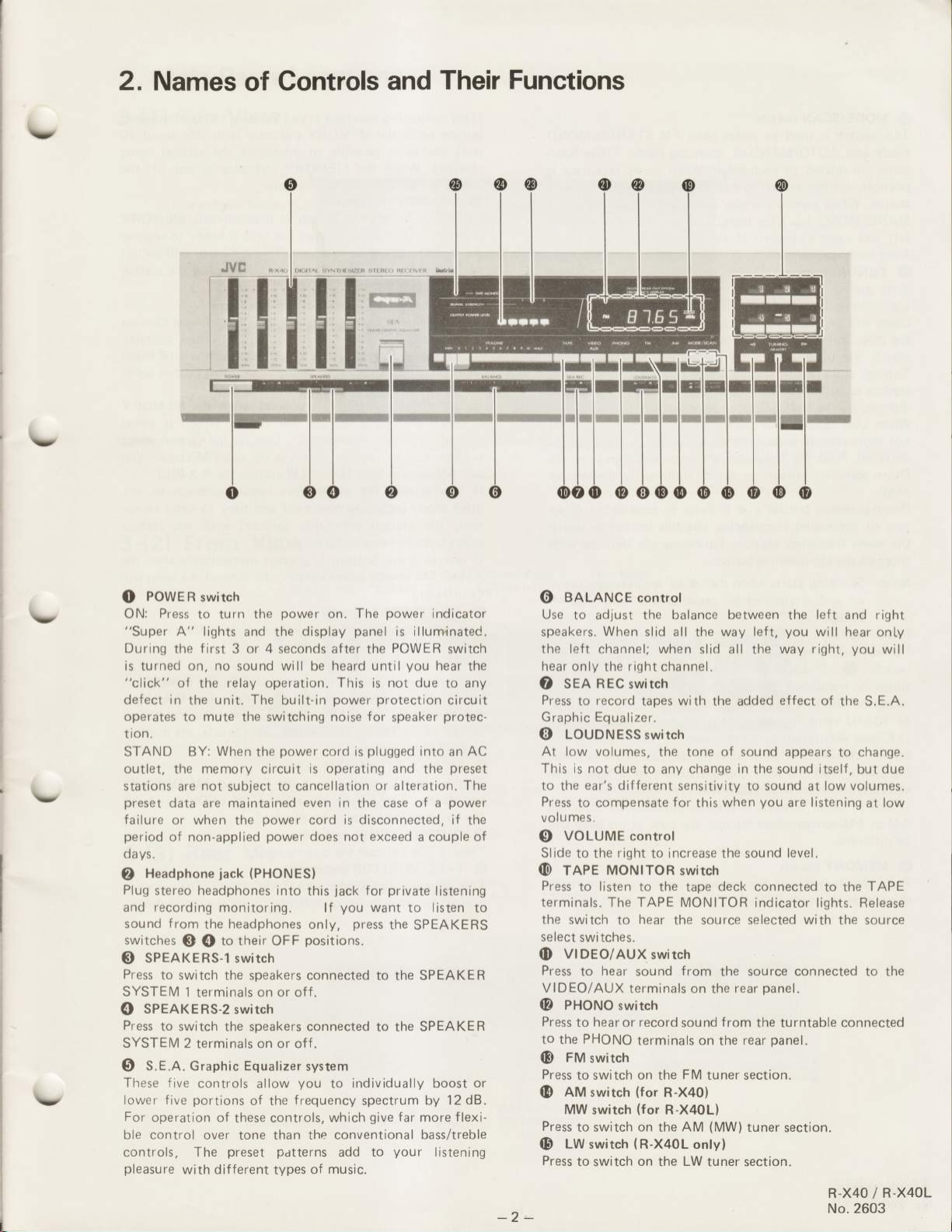
2.
Names
Gontrols
of
and
Their
Functions
(D
@
\,
\,
\,
\,
JVg
Rxa
iT
'l
I t.:
rI
POWER
O
ON:
"Super
Durinq
is turned on, no
"click"
defect in
operates
on.
ti
STAND BY:
outlet, the memory circuit
stations
preset
failure
period
days.
Headphone
@
Plug
and
sound
switches
spenreRs-l
€)
Press
SYSTEM
SPEAKERS-2
o
Press
SYSTEM
S.E.A.
O
These f
lower f
For
operation of
control
ble
controls, The
pleasure
switch
Press
to turn
A" lights
f
the
irst 3
of the relay operation.
the
mute
to
not
are
data
are
or when
of non-applied
stereo headphones into
recording
from
the
(}
O
to switch
1
terminals
to
switch the speakers connected
2 terminals on or off .
Graphic Equalizer
ive controls
portions
ive
over
with different
I
power
the
and the
or 4
seconds after the
will
sound
unit. The
When
subject
maintained
iack
monitoring.
headphones
to
the
preset pdtterns
built-in
tlre switching noise
power
the
to cancellation
power
the
power
(PHONES)
their
OFF
switch
speakers
on or off.
switch
allow
of the
these controls,
than the conventional
tone
types
:\\r,{\'/rR srrRr.
ln'i,{
on. The
heard until
be
panel
display
This
power protection
for
plugged
cord is
is operating and
even
in
the
is disconnected,
cord
does
this
only,
positions.
connected
system
you
f
requency
of
exceed
not
jack
for
you
want
lf
press
individually boost
to
spectrum
give
which
to
add
music.
*r'
\rx
power
indicator
is illuminated.
POWER
not due
is
speaker
or
alteration.
case of a
you
into
hear
the
switch
to
circuit
protec-
an
preset
The
power
if the
a couple of
private
to the SPEAKER
to the SPEAKER
listening
listen
to
the SPEAKERS
by 12
far
more f lexi-
bass/treble
your
listening
the
any
AC
dB.
gnLaNcE
@
Use
to adjust the
speakers.
the left channel; when
hear only
sen REC
O
Press
to
Graphic Equalizer.
LOUDNESS
O
At
low volumes,
This is not
ear's different
to the
Press
to compensate
mes.
volu
VOLUME
O
Slide
to the
(E
rnPe MoNlToR
Press
to listen to
to
or
terminals. The TAPE MONITOR
the switch
select
switches.
VIDEo/AUX
O
Press
to
VIDEO/AUX
(D
PHONO
Press
to
to
PHONO
the
(D
FM
switch
Press
to
(E
AU switch
MW
Press
to switch
(D
LW
switch
Press
to switch
control
balance between
When
slid all the way left,
the right channel.
switch
record
tapes
SWitCh
the tone
due
to any
for
control
right
to increase the sound
the tape
hear
to
switch
hear
sound
terminals on
switch
hear or record
terminals on the
switch on
switch
the
(for
R-X40)
(for
R-X40L)
on
the
(R-X40L
on
the
the
you
slid all the
with
the
of
change in the sound itself,
sensitivity
when
this
switch
deck connected
the source selected
from
the
the
from
sound
FM
tuner section.
(MW)
AM
only)
LW
tuner section.
way right.
effect of
added
appears
sound
sound
to
you
indicator lights. Release
at low
are listening
level.
with
source connected to
panel.
rear
the turntable connected
panel.
rear
tuner section.
left and
right
will hear only
you
will
the S.E.A.
change.
to
due
but
volumes.
at low
TAPE
to the
the source
the
R-X4O
No.2603
R.X4OL
/
-2-
Page 4
(D
MODE/SCAN
This
switch is used
mode and
are related
tions
possible,
tuning.
MANU/MONO
left
from
(E
Auto
Up-scanning button
beeps
the direction of increasing frequencies.
search the
Tuning)
station
digitally
When
not
detected. Press
Down-scanning
ning.
Down-scanning
tion
the
those of
set this switch
When
right channel
and
both speakers.
rurutruc
tuning
will
stops automatically when
is
by the
you
even
stop
of
decreasing
lower f requency
the Up-scanning button.
Note: Scanning starts when the
ed
switch.
Manual
Manual
switch
tuned-in
reception
or
U.K.
button
ing
scanning
tuning
tuning
@
frequency
kHz
10
Australia), or 1 kHz
and
changes the
(more
sequence
lf one of these
AM or
be different.
(D
Press
show
FM
MEMORY
this switch and
that this
switch
to select both
AUTO/MANUAL
each
to
signals
(^)
buttohs
be heard and
upper
pulled
in.
f
requency
continue to
if
broadcasts
the Up-scanning
button
button
is
and
stopped by
possible
is
Pressing
.
(50
kHz
for
steps
than
0.5 sec.) changes
which
buttons
source select button, the tone
switch
unit
other.
AUTo/sTEREo
to
are
too
for
manual
FM
signals
(
>
When
):
tuned-in
the
frequency
This
tuned:in
indicator.
press
select stations
to
(
1
frequencies.
station.
):
by
Up-Down-scanning
the
changes in 100kHz
for
steps
(MW) (9
AM
tuner step
stop
pressed
is
memory indicator
the
ready
is
FM
scanning
When
weak to be
tuning;
are mixed and
this
broadcast.
the
frequency is displayed
this button,
which
could
button
Press
Use
this
Functions
<
or
pressing
pressing
Europe,
kHz
for LW.
steps
by step,
tuning
when released.
immediately after the
receive a memory setting.
to
STEREO/MONO
mode. These
stereo
(r)
received,
in
this
button
frequency changes
Use this button to
Scanning
next
scanning
be tuned
and then
by
to tune
func-
reception
for
set to
mode the
heard
pressed,
is
(Auto
(or
FM
in are
press
down-scan-
in
direc-
the
auto
AM)
does
button to search
identical
are
> button
MODE/SCAN
th'e
MODE/SCAN
the
buttons, thti
steps
U.K., and
steps
Tapping
continuous
in
a
of
the
with
press-
is
for
Australia)
for Europe,
press-
high
speed
beep
will light
the
FM
this
will
(This
switch is a
button while
sec.) makes it
is
in
received.
memory
(D
When
indicator lights
the
automatically in
select button.
@
These
or
When
and the LED
function
MEMORY indicator
the
preset
Station select
buttons are used to select
memorize
to
one of
to indicate
lf
one of
switch
received
buttons can be used in common
one
lf
other mode including
tion,
select buttons
lf
AM or
be different.
O
This
in.
@
The
(kHz)
(D
will be "Memorized". One
AM
station
you
change the
the station
one of these
FM
FM
STEREo indicator
indicator
Frequency
tuned-in
are
(MHz) (for
four
or
ed
@
This is
broadcasts. The
the
@
These
(D
to
This
pressed
digits
for FM
stcrual
used in
stronger the
ourpur LEVEL indicator
LEDs
TAPE
indicator
for
non-lock
MEMORY indicator is lit
the
possible
When
MEMORY
MEMORY indicator
the
does not operate.
switch
to show that
station
to memory.
about 10 sec. or by
buttons/Station
the station
these buttons
indicator
which channel is
these buttons
is
(one
remains
source select
lights when an
indicator
frequency
displayed for AM
Europe,
(MHz) (for
reception.
STRENGTH
on
pressed
MW or LW
mode
power-off
previously
tuned
buttons
is displayed digitally.
U.K.,
tuning to
greater
signal being
indicate the output level.
MONITOR indicator
lights
monitoring or
the
when
type.)
Pressing
station select
the
(for
about
to memorize the station being
is not lit,
pressed,
is
unit is
the
This
indicators
one of
for
an individual
pressed,
is
the corresponding
in
operation.
pressed
is
in, the station
for
station
this
ready
indicator
pressing
the
beeps
when
the
which is
of
the station select
FM
one
for R-X40L).
from radio reception
and back to
selected
in.
pressed
is
button, the tone
FM
reception
Australia
U.S.A., and Canada)
indicator
both
number of
received.
the TAPE MONITOR
listening
with
immediately
of
stereo broadcast
and five
other countries)
and
FM
to the
and
tape
AM
LEDs
will
the station
preset
will be
button lights
station and
radio recep-
the station
the
Four
are
recordings.
the
MEMORY
register
to
go
out
stations
channel.
heard
MEMORY
being
to any
after the
beepwill
is
tuned
digits
digits
display-
(MW/LW)
light,
that
switch
10
\z
v
is
R-X4O
No.2603
R-X4OL
/
v
Page 5
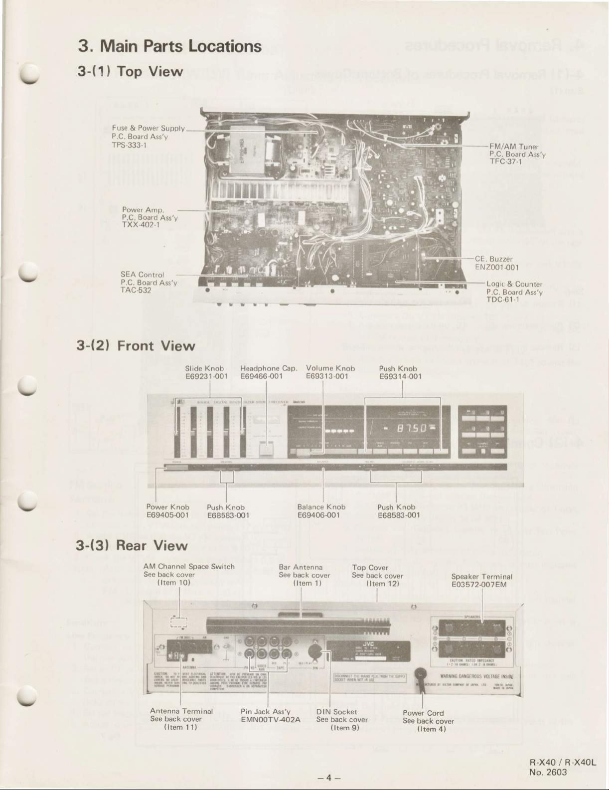
Main Parts Locations
3.
3-(11 Top View
\-
\,
Fuse & Power
P.C.
Board
TPS-333-1
Power
P.C.
TXXAO2-1
SEA
P.C.
TAC-532
Ass'y
Amp.
Board
Control
Board
Supply
Ass'y
Ass'y
3-l2l Front View
Slide
E69231-001
lrlrt
Knob Headphone Cap.
E69466-O01
Volume
Knob
E69313{01
Push Knob
E69314-O01
FM/AM
P.C.
Board
TFC.37.1
CE. Buzzer
ENZ001-001
Logic
&
P.C.
Board
TDC-61-1
Tuner
Ass'y
Counter
Ass'y
\-
fy
3-(31
Rear
AM
See
Power
Knob
E69405001
View
Channel
back cover
(ltem
Antenna
See back
-t
i--t
t--t-
(ltem
Space
1ol
I
I
I
Terminal
cover
11)
Push
Knob
E68583-001
Switch
Balance Knob
E69406.o01
Bar Antenna
See
back
(ltem
Pin
Jack Ass'y
EMN00TV402A
cover
1l
DIN
See
-4-
back cover
(ltem
Top
Cover
See
back
(ltem
I
I
Jwdmift-ffi-^rm
trlS rd
l@l
Socket
g)
Knob
Push
E68583.o01
cover
12)
(-
siil
J
Power
See
Cord
back
(ltem
Speaker Terminal
E03572007EM
rutm
il$tm{,s v0[IrG€ ilsts
nrGrrs
cover
4)
R.X4O / R-X4OL
No.2603
Page 6
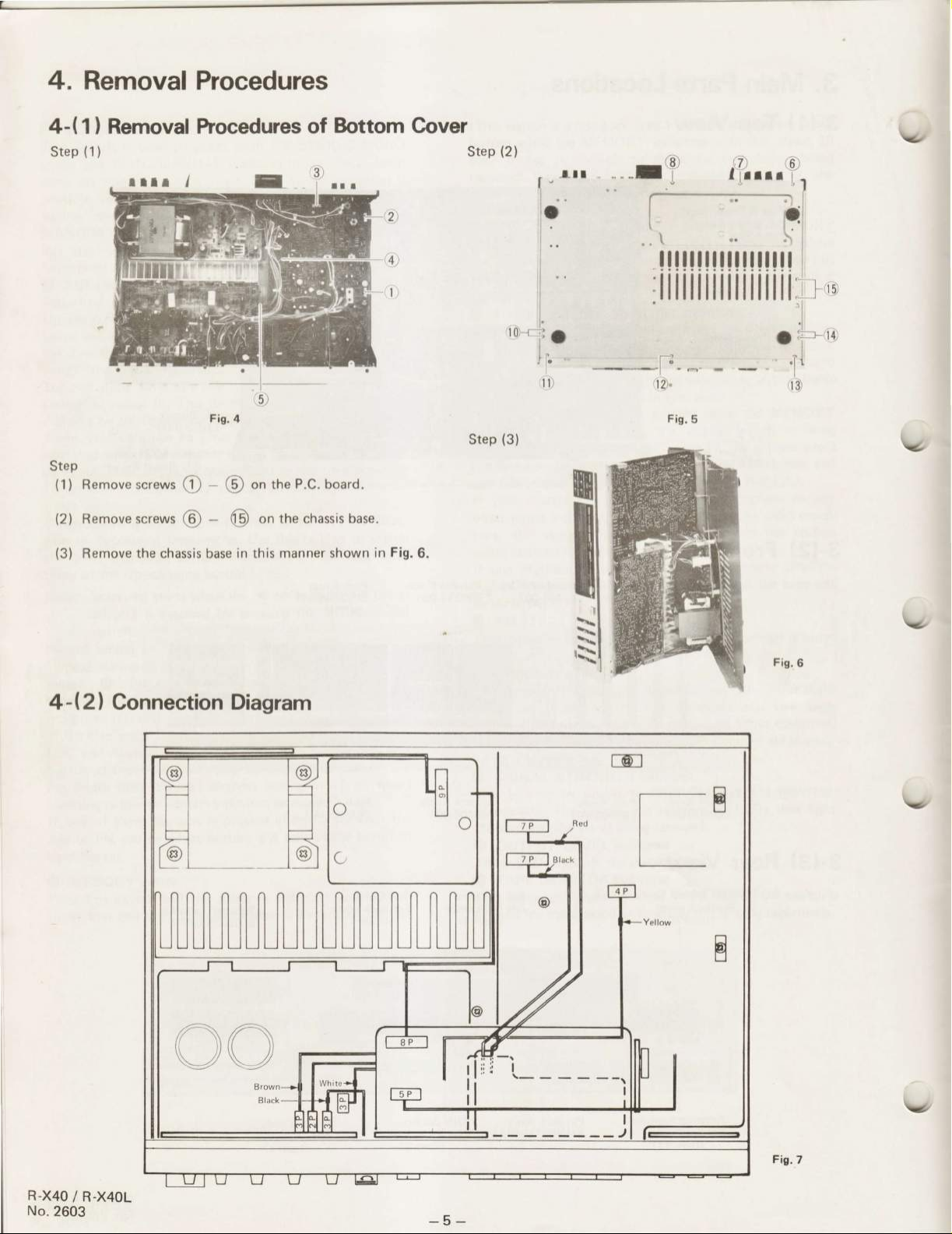
4. Removal
Procedures
4-11) Removal Procedures
(1
Step
)
r.5)
Fig.4
Step
(1)
Remove screws
(2)
Remove screws
(3)
Remove the chassis base
@
@
-
-
the
on
@
on the chassis base.
@
in
manner shown
this
of
P.C.
Bottom
board.
in
Gover
Fig.
Step
(2)
":"
1
iO
I'
\
fl,r..
..
ol
t.';
\r
\r/
f!fffftftfffrfffil i
llllll
llil ll il il il:,
t.
l0)--c-1
j
I
jir
'
rD
Step
131
6.
l.
t-fr--l
D-
oi
.l
'l
I
'1
"l
1
rs)
\z
4-l2l Connection Diagram
\r.
Fis.6
v
C
I
\-
-
-
_ _-\
I
\r'
R.X4O
No.2603
R-X4OL
/
-5-
Page 7
5.
Adiustment
Procedures
\-
\-
5-(1) FM/AM
(MW/LW)
o
Tr ro
Tuner Adjustment
Ltot
rf
\--l
cto2
@
r:\
Lr02
Tlot
Procedures
High Frequency
the RF
6. Set
1
kHz
ot 2
Set
1tY.
the
7.
8. Adjust the FM trimmers
9. Repeat these high and low
alternately
Descriminator,
Press
1.
to
2. Connect
75 kHz deviation to the
panel
through
3. Connect an oscilloscope, Distortion Meter
to the Rec.
4.
the
Set
minimize.
5.
the Frequency
Set
6. Connect a DC VTVM between TP1 1 1 and 1 12.
7.
Adjust the core indicated arrow A of T101
VTVM reading
And set the RF
8.
9. Adjust
distortion is minimized.
generator
and a deviation of 75 kHz to
Frequency
to 106 MHz,
Display to 106 MHz.
to
C102
maximize the output.
frequencies
a
provide
until maximum sensitivity is obtained.
Distortion and
position.
FM
RF
an
a dummy antenna.
jacks
out
generator
RF
of 0
generator
the
core
indicated
generator,
Signal Gain
antenna
on the
to 98 MHz,
Display
(zero)
output to 1 mV.
1 kHz
rear
to
mV.
arrow B of T101 so thatthe
modulation
terminals
panel.
generator
a 98 MHz.
modulation
input
an
adjustment
and a
on the rear
and VTVM
output to
for
DC
of
\,
\-
\-
sw305 sw507 sw306
sw302 sw304 sw305
Fig.8
FM Section
Band Cover
1.
the frequency
Set
display
2. Connect a DC. VTVM.
3. Adjust Ll03 so
4.
5. Check
set the frequency display
And
the
that the VTVM.
VTVM.
Note: After adjustment,
follows:
as
FM:
Sensitivity
Frequency
Low
1.
Connect an
the rear
2.
Set an
and a deviation of 75 kHz to
panel
RF
(for
Low-end 87.5
Hish-end 108.0 MHz
generator
RF
through a
generator
to 108.0 MHz.
points
to test
shows
to
87.5
voltage
reading
confirm
West Germany only)
MHz
that the band
-
300
+500
to the antenna terminals
dummy antenna.
to 90 MHz, a
provide
3. Connect a VTVM and an oscilloscope
jacks
on the rear
4.
Set
frequency
the
5. Adjust coils L101
panel.
display
L1O2
,
to
MHz.
90
to maximize the output.
117
and GND.
8.00V.
MHz.
t
V
kHz
kHz
input of 2
an
0.5 V.
cover
on
1tY.
1.60
modulation of 1 kHz
to the Rec. out
Multiplex
Multiplex
1.
2.
3. Connect a VTVM,
4.
5.
6.
7.
8.
is
Stereo Separation
9.
10.
1 1.
12.
13.
Stereo
14.
and
Stereo Separation
Set the stereo signal
modulation frequency,
kHz main
67.5
the RF
Connect an RF
through
meter to
Set
Set
Connect
TP1 08.
Switch
Adjust
Switch the selector of stereo modulator to left
modulation.
generator.
the RF
the frequency display to
off the
R181 so that the
19 kHz
(0
and sub carriers. Connect its
a dummy
the Rec. out
generator
the frequency
pilot
-50
-
Adjust R173 so that the output of
minimized.
Switch
modulation.
Adjust R173 so
Set R173
right is
the selector of
different.
threshold
that the left channel is minimized.
to
a average,
Adjust R143 so that
output
of RF
generator
generator
7.5 kHz deviation
generator
antenna.
an oscilloscope
jacks
to
98
counter to 19 kHz Test
signal of
frequency
Hz).
the modulator
if the separation of left
STEREO
10
follows:
as
to the antenna terminals
and a distortion
on the rear
MHz
98
stereo modulator.
pV.
panel.
and outputof 1
MHz.
counter
right
to right
indicator
lights
channel
400 Hz
pilot,
output to
mV.
Point
indicates
channel
channel
and
the
at
is
R.X4O / R-X4OL
No.2603
Page 8

AM(MWI
Band Cover
1.
2.
Section
Press
to AM(MW)
frequency
the
Set
step), or 522kHz
positign.
display to 520 kHz
(9
kHz channel stepl.
3. Connect DC. VTVM. to test
4.
Adjust L203 so that
5. And set the
ctannel step), or
6. Adiust G246 so
1710
kHz, or 7.50 V
the VWM.
frequency
1611 kHz
that the DC. VTVM.
for 1611
point
shorvs 0.85
display to
(9
kHz channel step).
kHz.
(10
117
and
1710 kHz
reads 9.00 V
kHz channel
GND.
V.
(10
kHz
for
LW Seetion
Band GoYer
to LW
frequency
position.
display
the
so that
display to 360 kHz.
to 153 kHz.
points
116 and GND.
VTVM. shows 1.20
Press
1.
2.
the frequency
Set
3. Connect a DC. VTVM. to test
4.
Adjust L2(X
5.
the
Set
6. Adjust C251 so that the VTVM. reads 8.00 V.
V.
Tracking and
1.
Connect
the rear
2. Set
modulation
3.
Set
4.
Adiust
Semitivity
the RF
panel.
generator
the
frequency
the
the core of
400 Hz.
at
generator
to
display to
ferrite
output.
generator
the
5.
Set
the frequency
Set
6.
14fl)
to
display of the
or 14O4 kHz.
7.
Adjust
Repeat
8.
maximum sensitivity is obtained.
so that the
C202
these adjustments
to the antenna
600
kHz
bar antenna
kHz,
output
(or
600
kHz)
603
kHz, or 603
to maximize the
or 14O4 kHz.
unit to 1400 kHz,
is
(1
signal
-
maximized.
7) alternatery untill
terminal
with
30 %
kHz-
on
Tracking
and
Sensitivity
1. Connect the RF
the rear
2.
Set
at 4(X) Hz.
3.
Set
4.
Adiust
the output.
5.
Set
6.
Set
7.
Adiust C209
Repeat these
8.
maximum
panel.
generator
the
frequency
the
the
frequency
the
frequency
the
selectivity is obtained.
generator
to the antenna terminal on
to 164 kHz with
display to 104 kHz.
core of
so
ferrite
generator
display
bar antenna to maximize
to
of the unit to 353 kHz.
that the output signal
adjustments
(1
30
kHz.
353
is
alternatery untill
-7)
% modulation
maximized.
R-X40 / R-X40L
No.26O3
-7-
Page 9
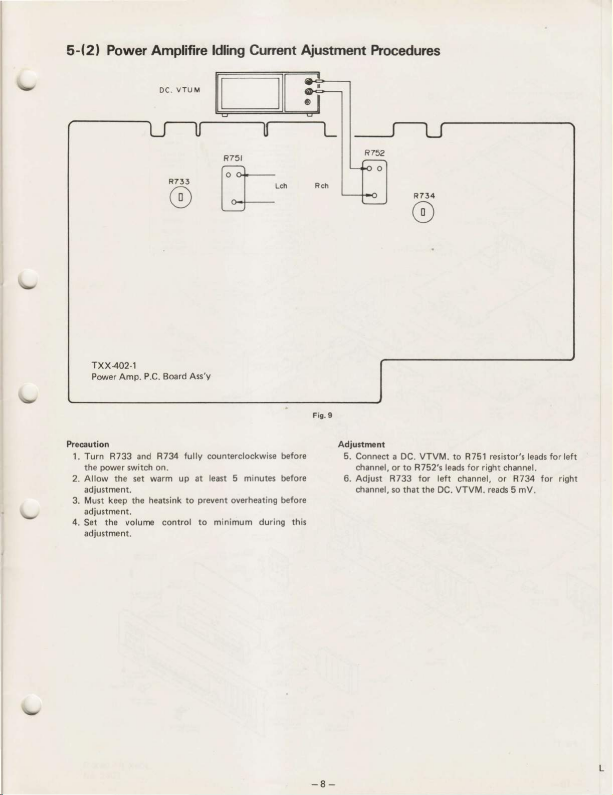
5-(21
Power
Amplifire
VTUM
DC.
ldling Cunent
f-"4-
Aiustment
Procedures
v
t-
1 \-,
I
J
I
)
,
/l
,1
TXX402-1
Power Amp.
Precaution
1. Turn R733 and R734
power
the
2. Allow
3.
4.
the set warm up at
adjustment.
Must keep the
adjustment.
the volume control
Set
adjustment.
P.C. Board
switch on.
heatsink to
@u-
Ass'Y
fully counterclockwise before
least 5 minutes before
prevent
to minimum during this
overheating
before
Fig.9
R734
@
Adjustment
5.
Connect a DC.
channel, or to R752's leads for right
6. Adiust R733 for left
channel,
VTVM. to R751 resistor's leads for left
so that the DC. VTVM. reads
channel.
channel, or R734 for right
5 mV.
lv
-8-
Page 10

Block Diagram
6.
FM
osc
Freq.
1c402
TDG1(}4P
ro101 Tc9147P
re|51 TD6301AP
RAM
FIVE + l,-art
Atvf
+
Lat CH.
CH.
7.2MHz
-l
l
X't
Raonator
Block Diagram of
PLL
Fis. 10
Syntherizer
-9-
R-X/[O
No.2603
R-X40L
/
Page 11

7.
Exploded Views
ai
$
and
Part
,4a'g&
''*-^'.
!{il{l
Numbers
a".'?
;,>?
'zt
\%
-<\
r\
v
Bil;r-'::"",
rrcder
i{p;f'*'
rr;"r,,,
"*i***:,--.*N
':"'
,z
"
."'><
2,
YB
"//
:\zZ./'..7..,^-,.,4
/',
,.7
\o/
'.{
,,._/
\
C.B. As'y
TXX.402.l
-
-
roo cov>
tuuckcover
{ltem
y'
/ /."'
12"-
-@n
''-Y----
t
_,a..
EMNOOTV
\
-
l2)
Grit
l.a'
-/
a'
/
_---N'
./
-
izt
-/'\
Antenna Term
See
cover
bck
(ltem
1 1)
-
-'?
h!
"-SrL*'.
,.t
FM/AM
and
rFc-37.1
l-
.rc)b Logic
ET2257.@1
Tuner
Lw)
lMW.
Phono
Eqnauzer C.B.
\ Sc'ew
\
Ast'y
sBsBmsz
and Couner C.A. Ar!
TDC61 1
EL!o@r 0r
F'onr
Puri
\ar
v
1
Pftl
A$' , Paft
---\\
SJilon Esc!icheon
lolure Knobl
'to.
(Super
'late
rtoi
-oudne$,
lro'S*akers,
SEA
Mode)
A
Li3t
Mdd
A)
EFP-8X4OE
8302260
E302203.003
E69307 @r
E24178 ml
E694@.001
E301773 001
E68636.001
Fec)
E69403
E30231 1.001
E692r2-m1
E60912.m3
R.X40 R-X40L
RX4OLE
EFP
E302260.@l
001
E302203 0g
E69307 @r
E241JA@1
€6gq @1
E301773.001
E6S36 @l
@1
E69403 m1
E30231 1 00r
E69212 m1
E6G12.m3
Al'
,ir
?**,
-,^a
pnndy
covn
itr#*l;;;
V
-,^ir-i*x'#;;".","-",,
K-
€302266.00r
)>
%ry'"
\ )Y/tl
PowerTrantormer
&.bacrcovfl \
llren15,
E653S m2 E69416 @'
\ \
-/
V
\ ,,t ," I
,/
./
1
-/
t
-/
,t-.&rew
sBsB3mz
-.
\-Y-r<\
Fig.
\Z
a\---\rp\s2604\ 2
?r)t<.-\\{,,*,,r,"lf
\Z\ *1"1.;\
.r..--.-\\il1ifi,1,1"i:"'\
r9.@r
E6st
l1
I
\-\t-
screvi /' ,/
r
E65t t9.OOl
>>'AZ,*
\
\
!r'.r- \
\i;';r;ii6ll
\
\-'\
:",ri,*"\
\ W
-R2
p.wpr
Knob
F6C!O6 0n1
\-'
:[$5i;3i'
I -
-(-i.ir,
E36,:dd".i.\
:bi*[;r:u
*€ bd
LED
E6913-m1
5.-s*,.n
:i;irciii:qjr
U)n
a,,(
-al'
€6$I
11
. .i
Holder
oo,t-
A,
Scale
I
E302264 001
E48729.m
I
I
-
lE6948so1
A
R.X4O / R.X4OL
No.2603
-10-
Page 12

8. Printed Circuit
Board
Ass'y
and
Part List
1
8-(
Note:
TFC-37
l
TFC-37I-1 varies according
@
!
FM/AM
(MW
to the
LWI Tuner & Phono
areas
employed.
See
note
TFC-37ffi
(l)
Equalizer P.C. Board
Ass'y
Each lndividual P.C. Board Location
Fis. 13
Fig. 12
(1)
Note
Desionated Areas
U.S.A.,
Market & Other Countries
Europe
W.
U.K.
Note
@rrc-sz-r
@rcc-st-z
Germany
(2)
Canada,
& Australia
The symbols
surface
Tuner &
DIN Terminal
U.S.
are
Equalizer
Military
(
x. t,
factory
P.C.
P.C. Board Ass'y
etc.) on
8...
process
only.
P.C.
Board Ass'y
Board Ass'y
TFC-37A-1
TFC.37B.1
TFC-37C-1
TFC-37D-1
P.C.
Board
-11
R-X4O
No. 2603
R.X4OL
/
-
Page 13

Transistors
Item No Part
0101
0102
0103
0104
0105
0106
o107
0108
0109
ol
0111
o201
0202
o203
0204
o205
o206
4207
0208
o209
lntegrated
tem No Part
rc101
rc102
rc201
tc301
2SK168(E, F
2SC535(8,
2SC461
2SC461
2SK168(E. F
2SK168(El
2SC535(8,
2SC458(Ol
2SC458(C, D)
10
2SC458(C, D)
2SC458(C, D)
2SK105(F, H)
2SK105(F, H)
2SC458(C.
2SK105(F, Hl
2SC458(C.
2SC458(C, D)
2SC461
2SK105(F, H}
2SK105{F, Hl
HA11225
LA3390
LA1245
NJM4558D.D
Circuit
Diodes
Item
No Part
D101
1 S1
D102
D105
D202
D204
152076-31
1
52076-31
1
52076-3 1
1
52076-3 1
1 52076-31
1
52076-31
1
52076-31
1 S2076-31
152076-31
'ts2076-31
1S2076-31
SVC2O2(AB)
SVS2O2(AB)
SVC2O2(ABI
KV12362
KV12362
KV1236Z
KV1236z
Dl04
D201
D203
D205
D206
D207
D301
vc101
vcl02
vc103
vc201
vc202
vc203
vc204
Coils
tem No Part
LI
EOR2306{14
UI
Ll01
EOR2306€16
L102
EOR2306011
L103
EOR2406{02
L104
EOL3001-1
Number
Number
Number
88FM
Number
(8,
(8.
(B,
C)
Cl
Cj
C)
D)
D)
C)
RSKY
Ratinq
F.E.T.
Silicon
F.E.T.
Silicon
Descriotion
Maker
Hitach
"
F.E.T
Silicon
F.E.T.
Silicon
F.E.T.
Rating Description
t.c.
Rating
Silicon
V. Capa.
Diode
r.r;.
"
Hitachi
NEC
Hitachi
"
"
NEC
"
Maker
Hitach
Sanyo
Dainichi
Description
Maker
Sanyo
Hitach i
"
"1"
,,( ,,I
,,',1
"
Sanyo
Toko
"
"t "
Rating
Description
RF
Coil
"
I nductor
(for
(for
A,
Cl
(for
(for
(for
(for
{for
(for
(for
(for
(for
(for
(for
(for
B, D)
I
,,
C
D)
D)
Dl
D)
D)
D)
D)
Dl
D)
I
I
D)
D)
l
Coils
Item No
L201
L202
L203
L204
T101
T102
T201
cF101
cF1 01
cF102
cF1 02
cF201
cF202
LFlOl
LF102
Part
EO13001-101KY
EOu001-102KY
EORl
EOR1307002
E03793{O1
EOF0102{01
EOT1021{O1
EC821
ECB21
ECB2123{o2R
ECB21
ECBl
E03613-002
EO3427Q20
EO3427420
Capacitors
Item No Part
1
cl0
ocs3l
c102
oAT2001{01
c102
cl03
cl04
c105
c106
cl08
cl09
cl 10
c1 11
cl12
c1 13
cI14
cl
c1 16
cl17
c1 18
c1 19
cl20
c121
c122
c123
c124
cl25
c't26
c129
c130
cl31
c133
c134
c135
cl35
c136
c1
c138
cl38
c139
c140
c141
c142
c143
c144
cl47
c148
c149
cl
c152
cl53
cl54
ocs3l HJ-2R02
ocF3l
ocF3l HP-l032
ocF31
ocs3l
ocF31
ocs3l
ocs3l
ocs31
ocs31
ocF31
ocF31
15
ocF3l
ocF3
ocF3l
ocT25UJ-1002
ocT2SUJ-2202
ocs3l
ocT25UJ-5R02
ocT25UJ-5R02
ocs31
ocs3l
ocF3l
acF3lHP-2232
ocF31
ocs3l HJ-2202
acF3lHP-2232
ocF3lHP-2232
acF3lHP-2232
ocs31
ocs3l
oET6l HM-1052M
37
acF3lHP-2232
oET6l
oET6l
acrc1HP-2232
oET6lCM-4762M
acF3lHP-2232
acF3lHP-2232
ocF3lHP-2232
oET5l
oET6l
oET6l HM-4752M
cET61
51
acF3lHP-2232
aETSlCM-227
xET6l
f,FM31HK.6EJIIZ
Number
207{03
23{02R
1 8{)01 R
t8{O1
545{01
Number
HJ-2R02
HP-l032
HP-1032
HJ-5R02
HP-l032
HJ-4R02
HJ-1002
HJ-4R02
HJ-l512
HP-l032
HP-l032
HP-1032
HP-1032
1
HP-1032
HJ-7R02
HJ-4R02
HJ-2R02
HP-l022
HP-1032
HJ-l
51 Z
HJ-3302
HM-l062M
HM-4752M
CM-227
EM-1062M
HM-4752M
HM-4752M
R
0.01
5pF
0.01
'l
0.01
rO
22
7pF
u.lt
2pF
lOOO oF
O.O22
0.01
22
O.O22
rSO
33
1pF
O.O22 uF
10
4.7
O.O22
47
O.O22
22O
10
4.7
O.O22
22O
4.7
0.068
Rating
Ratinq
2pF
50 V
2pF 50 V
pF
',:,
pF
4pF
pF
1O
4pF
pF
50
pF
pe
pF
":'
4pF
pF
pF
pF
pF
pe
pF
pF
pF
pF
16 V
rrF
p,F
50 Y
16 V
ttF
pF
25V
pF
50 V
pF
pF
16 V
50 V
rtF
pF
Description
"
"
"
"
"
"
"
(for
(for
(for
D)
(for
Al
(for
B, C, D)
(for
Al
(for
B,
A,
ffor
fteccrintinn
(for
C)
(for
A,B,D)
(for
C)
(for
(for
A,B,D)
(for
("
D)
D)
C,
B, C)
Dl
C)
C)
lnductor
FM DET-Transformcr
Filter
l.F. Transformer
Filter
MPX Low Pass Filter
Ceramic
Trimmer
Ceramic
"
Electrolytic
Corrmin
Electrolytic
"
Ceramic
Electrolytic
Ceramic
ei""t.oryti"
"
"
C"r"-1"
Electrolytic
Mylar
V/
\(r
Yt
Yt
I
Y
R.X4O / R.X4OL
No.2603
_n _
Page 14

r>
>
:
Y
Capacitors
Item No Part Number
c1
ocs3
c1 55
cl 56
cl 56
c1 59
c160
c161
c162
c163
cl64
cl65
cl
67
c168
c201
c202
c203
c204
c205
c206
c207
c20B
c209
c210
c211
c212
c213
c214
c215
c216
c21A
c219
c220
c22'.\
c222
c223
c224
c225
c226
c227
c22A
c229
c230
c231
c232
c233
c234
c235
c236
c237
c23A
c239
c240
c241
c243
c244
c245
c246
c247
c248
c249
c250
c251
c252
c253
c256
c301
c302
c303
c304
c305
55
HJ-561
1
ocY3
HK-8212
t
ocs31 HJ-5612
ocY3l HK-821
ocY2l
HK-103
ocY21
HK-103
oFM3l HK-4732
oEB51 EM-225
oEB5l EM-335
oFP31 HJ-102
oE20046-105
oET6l HM-4752M
oET6l HM-4752M
ocs31 HJ-sR0z
oAT2001-005
ocF3lHP-2232
ocF3lHP-2232
ocY31 HK-l022
acF3lHP-2232.
acF3lHP-2232
ocs31 HJ470Z
oAT2001-005
acF31HP473Z
ocF3lHP-2232
ocY3lHK-2222
ocF3lHP-2232
ocF3lHP-2232
ocF3lHP-2232
ocs31 HJ-181 Z
ocY3l
HK-l022
x.cF31HP-2232
acF3lHP-2232
JCF3\HP-2232
f,ET61 CM-2262M
f,cs31 HJ-5602
).cF31HP-2232
1CS3
HJ-l
1
).cF31HP-2232
).cF31HP-2232
acF3lHP-2232
)cF31HP-2232
1CY31
HK-1022
)cF31HP-2232
f,ET61HM-1052
fET61 HM.475Z
)cF31HP-2232
acF3lHP-2232
f ET61 HM-1052M
f,ET61
CM-4762M
)cF31HP-2232
]FM31 HK-4732
acY3lHK-4722
fFM3l HK.473Z
fcs31 HJ-221
)cs31HJ-2212
fcs3
1 HJ-1
fAT2001 -005
)cF31HP-2232
)cs3
1 HJ-l
)cs3
HJ-8202
1
f,cs31 HJ-8202
fAT2001
005
)cY21 HK-103
)cF31HP-2232
fcs3l HJ-8202
)cF3',
HP-2232
)cF3',
HP-2232
)cF3',
HP-2232
fcF3',
HP-2232
fET6,
HM-4752M
21 Z
802
01
Z
560
820
560
Z
820
0.01
O.O47
2.2
3.3
a.,!
5pF
O.O22
1 0O0
O.O22
47
0.047
O.O22
22OO
O.,O22
180
1
o;,?,t"'
22pF
56pF 50V
O.O22
12O
o|?,'2
1000
O.O22
1pF
4.7
O.,O22
1
47pF 16V
O.O22
O.O47
47OO
O.O47
Z
22O
18
O.O22
Z
100
82
0.01
O.O22
82
O.022
4.7
Ratinq
pF
50 V
pF
pF
pF
pF
pF
pF
25 V
pF
1000pF 50 V
u9 u
ue
50
ttF
pF
pF
pF
pF
50 V
ttF
pF
p.F
pF
pF
000
l:
16V
pF
pF
u'
pF
p,F
pF
pF ',:,
ttF
pF
50 Y
u.F
pF
ttF
pF
pF
pF
50
pF
pF
pF
50 V
rrF
pF
pF
pF
Ceramic
"
"
"
tVlylar
Low Leak Current
Electrolytic
Polvoroovlene
Nonflamable
Electrolytic
Ceramic
Trimmer
V
Ceramic
Trimmer
Ceramic
Electrolytic
Ceramic
Electrolytic
Ceramic
Electrolytic
Ceramic
Mylar
Ceramic
Mylar
Ceramic
Trimmer
Ceramic
,,
"
"
Trimmer
Ceramic
"
Electrolytic
Description
(for
B.C,Dl
(for
A)
(for
B,C,D)
(for
A)
for D
(for
t
for D
(foi
D)
(for
D)
(")
("1
(")
(")
(
"I
(for
D)
(for
D)
(,,|
("1
t" l
(for
D)
(for
C)
Capacitors
tem No Part Number
c306
c307
c308
c309
c310
1
c31
c312
c31 3
c314
c31 5
c316
c317
c31
I
Resistors
Item No
R
o1
R
o2
R
03
R
o4
R
o5
R
06
R
06
R
o7
R
08
R
09
R
10
R
11
't4
R
R
15
R
16
R
17
R
18
R
19
R
20
R
21
R
22
R
23
R
24
R
25
R
26
R127
R130
R131
R132
R 133
R134
R135
R136
R137
R1
38
F(
IJ9
R140
R141
Rl42
R143
R144
R147
R148
R149
R1
50
R1
51
R152
R153
Rl54
R1 s5
R156
R1
57
Rl58
R159
R160
HM-4752N
f,ET61
1CS31 HJ-331 Z
xcs3l HJ-3312
ccs3l HJ-5602
HJ-5602
xcs31
oFM31 HK-t 822
HK-l822
oFM31
OFM31 HK€822
OFM31 HK€822
oET61 HM-1052M
HM-105ZtV
oET61
oET6l
CM-476ZIV
oET6l CM-4762V
Part
Number Ratinq
oRD141J-473S
oRD141J-102S
oRD141J-270S
oRD141J-221S
oRD141J-473S
oRD141J-3025
oRD141J-472S
oR D141J-153S
oRD141J-102S
oRD141J-102S
oRD141J-3325
oRD141J-271S
oRD149J-101S
oR D141J-102S
oRD149J-470S
ORD
4(
)J-101S
ORD
4'
I J-1 03S
ORD
4'
ORD
4'
ORD
4
I J-220S
ORD
4
ORD
4
ORD
4
ORD
4
ORD
4
ORD
l4
ORD
t4
ORD
t4
ORD
l4
ORD
t4
ORDl4
ORD14
ORD14
ORD14
ORD14
ORDl4
tJ-4725
ORDl4
rJ-561S
ORDl4
I
ORDl4
rJ-3325
OVP4AI
)B-223
oRD149J-101S
oRD141J-103S
oRD141J-334S
oRD141J-823S
oRD141J-2225
oRD141J-472S
oRD141J-2725
oRD141J-473S
oRD141J-561S
oRD141J-2205
oRD't41J-473S
oRD141J-103S
oRD141J-4725
oRDX 41J-473S
oRD149J-101S
J-2225
J682S
J-1 055
J-391S
J-1
055
J-331
J-562S
J-2225
J-101S
J-2225
J681S
J-101S
J-1 02S
J-331
J-101
J-1
03S
J-33 1S
J-243S
4.7
330
56
1
800
6800
luF
47pF 16V
47
1ka
27n
220 dt
47 kf,
3ka
4.7 kO
15
'I
3.3 ksl
270 a
100 s2
1kO
47o.
100 Cl
10
2.2 k{t
6.8
22a
1Ms}
390
'I
S
330 s2
5.6 ka
2.2
100 sr
2.2
680 c,
100 f,l
1kf,
S
330
100 s,
S
10 ko
330
4.1 kA
560 a
24
3.3
22ka
100
10
330
82
2.2 kA
4.7 ka
2.7
47 kC2
s60 s,
22 dt
47
10
4.7 ka
47 ka
100 ko
pF
pF
kA
ko
kO
Mo
Ratinq
pF
pF
pF
kc,
ka
rl
ka
ka
s,
sl
ka
ks,
',
ks,
ksl
ks,
ka
ka
ko
El
V
50
',:,
ectrol
Ceramic
"
Mylar
Electr
1l4W
Carbon
"
"
"
U. Carbon
Carbon
U. Carbon
Carbon
0.1 W Variable
114w
U. Carbr
Carbon
1l4W
Carbon
U. Carbon
Description
ytic
(for
C)
("1
Description
(for
A,B,D)
(for
C)
(for
A,B,D)
)n
(for
C)
"I
"I
:")
l
tJ
R-X4O
/ R.X4OL
No.2603
-
Page 15

Resistors
Item No. Part Number
R162
R163
R164
R165
R166
R167
R168
R169
R170
R1
R
R
R
R
R
R
R
R
R
R
71
72
73
75
76
77
7a
79
80
81
a2
Rl83
R187
R188
R189
R201
R202
R203
R204
8205
R206
R207
R208
R209
R21
R211
R212
R21
R214
R215
R216
R217
R218
R219
R220
R221
R222
R223
R224
R225
R225
R226
R227
B228
R229
R229
R230
R230
R231
R232
R233
R236
R237
R238
R239
R240
R241
R301
R302
R303
R304
0
3
fRD141J-474S
fRD141J-184S
f,RD141J-273S
fRD141J-9135
fRD141J-9135
f,RD141J-274S
fRD14't J-2745
f,RD t 41J-100S
f,RD141J-100S
f,RD141J-l02S
oRD141J-102S
ovP4A0B-473
aF.DI41J-2225
oRD141J-2225
oRD141J-682S
oRD141J-6825
oRD141J-102S
oRD141J-l
ovP4A0B-103
oRD141J-563S
oRD141J-473S
oRD141J-473S
oRD141J-473S
oRD141J-153S
oRD141J-103S
41J-331S
ORD
41J-561S
ORD
41J-5625
ORD
ORD
4 1 J-1 03S
ORD
41J-2245
oRD141J-331S
oRD141J-562S
oRD141J-561S
oRD141J-5625
oRD141J-l02S
oRD141J-104S
oRD141J-1 52S
oRD14't J-271S
oRD141J-562S
oRD141J-101S
oRD141J-1 53S
oRD141J-223S
oRD141J-l02S
QRD141J-562S
oR D141J-223S
oRD141J-331S
oRD141J-103S
oRD141J-l03S
oRD141J-820S
oRD141J-221S
oRD141J-183S
oRD141J-104S
oRD141J-123S
oRD141J-5625
oRD141J-223S
oRD141J-l03S
oRD141J-182S
oRD141J-223S
oRD149J-101S
oRD141J-3325
ORDl4
ORD14
ORD14
ORD14
J-1
J-562S
J-1
ORDl4
ORDl
ORDl
ORDl
ORDl
ORDl
23S
04S
04S
J-2235
J-223S
J-l
03S
J-2225
J-2225
J-563S
J-563S
Rating
470 ko 114W
ks,
180
27 kA
ks,
91
ko
270
10f,
1ko
ka
47
2.2
6.8 ko
0.1
ka 114W
1ko
12 ks2
ko 0.1
10
ko 114
56
47 k9
kO
15
ko
10
s,
330
s)
560
kO
5.6
10 kfi
220 ka
s2
330
kO
5.6
a
560
ks}
5.6
1ks)
ka
100
1.5 ko
A
270
5.6 ko
100 s)
kf,
15
ka
22
lkO
ka
5.6
22 ka
rl
330
ko
10
82sl
220 a
18 ko
ko
100
kO
12
ko
5.6
22 kdt
10 ksl
1.8 ko
22ka
100
s,
ks}
3.3
100 ko
5.6 ko
ko
100
22ka
10 ko
ka
2.2
ko
56
W
w
W
Carbon
Variable
Carbon
Variable
Carbon
"
":.
"
"
"
"
"
"
"
U. Carbon
Carbon
(for
for D)
"I
"I
,,
,,}
,,
',
,,
',
"I
(
"
(for
("
(for
(for
(")
(")
(for
(for
|"|
(for
(for
(for
(")
(")
(")
(")
C)
D)
',}
',
,'}
',
,,}
A.B,C)
D)
A,B,C)
D)
A,B,C)
D)
D)
Resistors
No Part Number
Itom
R305
oR D141J-681S
R306
oR D141J-681S
oRD141J-393S
R307
oRD141J-393S
R308
R309
oRD141J-474S
oR D141J-474S
R31 0
R31 1
oR D141J-101S
R31
oRD141J-101S
2
R313
oR Dl41J-104S
R314
I
I
I
I
I
I
1
I
I
Others
Item
oRD141J-l04S
oRD149J-101S
R31 5
R316
oR D149J-101S
R318
R31
R319
R320
F'321
R322
R323
R2,t7
R328
R329
R330
SW3O1
SW3O1
sw302
SW302
sw303
SW303
sw304
SW3(M
SW305
sw305
SW306
sw306
SW3O7
SW3O7
Pl
01
P102
P
03
P
o4
P
05
P
06
P
07
P1
08
P1
09
s401
s402
D1
oR
oRD141J-l24S
9
ORD141J.B21S
oR D141J-103S
oR D141J-l03S
oRD141J-472S
oRD141J-4725
oRD141J-3325
oR D141J-3325
oRD141J-3325
oRD141J-3325
No Part Number
E03s72-016
EM89l
EMNOOTV.402A
E03623003
osTl6s1
osT1651
osTl
osTl 651
osTl
osT1651
osTl
osTl651
osTl
osTl
osTl 651
osTl651
osT1651
osT1651
oMV5005-007
oMV5005-007
oMV5005-002
oMV5005-003
oMV5005{04
oMV5005-002
oMV5005-003
oMV5005-003
oMVs005{02
EWSo15-072
EWSo17-043
E65396-001
E69328-O01
E1 0737-OO1
J-l
41
YV-201
651
651
651
651
651
24S
A
-E02
-E01
-E02
-E01
-E02
-E01
-E02
-E01
-E02
-E01
-E02
-E01
-E02
-E01
Ratinq
o 1t,:w
680
ksl
39
470 ks}
100 sl
100 ko
s}
100
120 ks)
s,
820
ko
10
4.7 kO
3.3 kn
Flrtind Itpscrinfion
Dessiotion
Carbon
U,. Carbon
(for
t" l
(for
Socket
B,C,D)
Switch
(for
A.B.C)
D)
lfor
A.B,C)
lfor
D)
ifor
A,B,C)
lfor
D)
lfor
for A,B.C)
B,C,D)
A,B,D)
(for
Carbon
"
Antemm Terminal
"
Pin
Jack Ass'y
DIN
(for
Push
for D)
for A,B,C)
for
D)
for A,B,C)
(for
D)
A,B,C)
lfor
(for
7P Plr
2P
3P
4P Plug Ass'y
2P
3P
2P
Socket
"
Earth Plate
Shield
Circuit Board
D)
rg Ass'y
Plug
Ass'y
Plug
Ass'y
Plug
Ass'y
Plug Ass'y
Plug
Ass'y
Wire
Cover
(for
(for
(for
Ass'y
(for
(for
\,
v
\r,
C)
\,
D
A
D
B)
A)
\r,
R.X4O / R.X4OL
No.2603
_U _
Page 16

8-l2l TXX-4O2[ Power
Amplifire
P.G.
Board
Ass'y
Note: TXX402E-1 varies according
to
the areas
employed.
See
note
(1)
@l
'-)
"'"
ol
1
Y
I
(,
r
U
o
o
o
o
o
Eacfi lndividual
P.C. Board Location
Fig. 15
Fig. 14
Note
OfXX+OZ-l
@TXX+OZ-2
@TXX+OZ-3
Note
Derignated Areas
U.S.A.,
Market & Other Countries
U.K.,
W. Germany
Canada,
Europe
(2)
U.S.
& Australia
The symbols
surface are
Power
Speaker
Headphone
Military
factory
Amp.
Terminal
Jack
(
#,
P.C.
Board Ass'y
P.C.
P.C.
P.C.
e...
f,
process
Board As'y
Board Ass'y
Board Arr'y
TXX4O2 A.1
TXX4O2
TXX4O2 C
etc.)
only.
on
B
P.C.
Board
-15-
R-X40
No.2603
R-X40L
/
Page 17

Transistors
tem No
o701
4702
o703
4704
o705
o706
0707
o708
o709
o710
o71
4712
o713
a7'14
o71
0716
0717
o718
o719
0720
4721
Q722
0723
4724
4725
4726
4771
4772
4773
0774
0775
0776
Q777
0778
o801
0802
0803
o901
0902
0903
lntegrated
tem No Part
tc701
tc702
tc901
Part
25C2240
25C2240
25C2240
25C2240
2SA1084
2SA
2SA
25A
25A
25A
1
2SC2546
2SC2546
2SD636
2SD636
5
2SC1775AV
2SC177sAV
2SA872AV
2SA872AV
2SC223s
2SC2235
254965
25A965
2SD1't48LB
2SD1148LB
258863LB
258863LB
2SC945A
2SC945A
2SC945A
2SC945A
2SA733A
2SA733A
2SA733A
2SA733A
2SD313V
2SC945A
2SB507V
2SC17754V
2SC1775AV
2SA872AV
Circuit
vcs022
vc5022
TA7317P
Diodes
Item No Part
D701
1 S2076-31
D702
152076-31
D761
RD9.1EB3
D771
1
D772
D773
0774
D801
D802
D803
D804
D805
D806
D807
D81 1
D901
D902
D903
D904
D999
S2076-31
1S2076-31
1
S2076-3 1
1 52076-31
s3v20F
53V20F
53V2OF
53V2OF
RD16E83
RD16E83
1
52076-31
1
52076-31
1
52076-3 1
1 32076-31
1S2076-31
1 52076-31
1 52076-31
Number
A,
B}
Rating Description
Silicon
A, B)
A, B)
A,8)
D. E)
(D.
084
084
084
084
084 {D- El
E)
(O.
E)
E}
{D,
(O,
El
(E.
F)
(E,
F)
(O,
R)
(O,
R)
(F)
(F)
(E}
(E)
(O,
Y)
(O.
Y)
Y)
{O,
(O,
Y)
(R,
O
(R,
O
(R,
O)
(R,
O)
(P,
O)
(P,
O)
(P,
O)
(P,
O)
O}
{P,
O}
{P,
(P,
O)
(P,
O)
(D.
E)
(P,
O)
(D,
E)
(F)
(F)
(E)
Number Rating
(x,
Y)
Y}
lx,
Number Rating Description
Silicon
Matsush ita
D€scription
Maker
Toshiba
Hitach i
Hitach i
Toshiba
NEC
Sanvo
NEC
Sanyo
Hitach i
Maker
l-{ohm
Toshiba
Maker
Hitach
NEC
Hitachi
NEC
Hitach i
Coils
Item No Part Number Ratino
L701
EOL0101
EOLO101-1R2
L702
-1
R2
Capacitors
i
tem No
cA)1
c702
c703
c704
c705
c706
c707
c708
c709
c71 0
c711
c7't2
c713
c714
c715
c716
c717
c71 8
c761
c762
c763
c801
c802
c803
c804
c805
c806
c807
c808
c809
c81 0
c901
c902
c903
c904
c905
c€06
c998
c999
Resistors
tem No
R701
R702
R703
R704
R705
R706
R707
R708
R709
R71
R71 1
R7't2
R71
R714
R71 5
R71
R7't7
R71
R71
R720
Part Number
f,ET51
HM-475
fETs1 HM-475
fETSl AM-476
f ET51AM-476
f,FM81HK-272
fFMSl HK-272
)FM81HK-332
)FM81HK-332
)cs21 HJ-7RoA
fcs21 HJ-7R0A
HJ-4702
fcs31
f,cs31 HJ-4702
)cs3 1 HJ-4702
)cs3
HJ-4702
1
fFMSl HK-473
fFMSl HK-473
f,FM81HK-473
f,FM81HK-473
f ETs1 EM-l06
f,EH61HM-1072
f,EH61 HM-4752
1EW81HA-878
fEWSl HA-878
)FM82AK-4732
JFMS2AK-4732
HP-4732
f,cF31
)cF31HP-4732
AEHilEM-227
HP-l
f,cF2 t
f,EH-51EM-107
03A
fcF21 HP-103A
acF21HP-223A
)cF21HP-223A
f,EH51HM-226
f EH51AM-107
f,ET51CM-226
f,ETs1HM-l05
fE20046-105
fcF21 HP-l
Part Number Rating
oRD141J-222S
oRD141J-2225
oRD141J-473S
oRD141J-473S
oFlDl4q t-rn?s
oRD149J-2025
oRD149J-202S
oRD149J-202S
oRD141J-101S
0
oRD141J-101S
oR Dl41J-472S
oRD141J-472S
oRD141J-272S
3
oRD141J-272S
oRD149J-101S
oRD149J-101S
6
oRD149J-390S
oRD149J-390S
I
oR D149J-3905
I
oRD149J-3905
02A 1000
Coil
Ratino Description
pF
4.7
47,lF
27O0
33,00
pF
pF
50
't9l
50 V
',:,
V
V
Electrolytic
Mvlar
7pF Ceramic
pF
47
pF
Q.O47
10pF 25V
pF
100
870O
0.047
50
r.rF
pF
',,,
22O
0.01
t00
0.01
o.o22
22
'100
22
1pF
z.z
47 k{t
tuo
100 fi
4.7
2.7
100 n
ttF
pF
pF
pF
pF
pF
pF
trF
pF
KsL 114
kO
kA
25V
Mvlar
Electrolytic
V
100 V Mylar
Ceramic
T,v
Electrolytic
V
Ceramic
50
25V
50 V
10 V
Electrolytic
Ceramic
',:,
Electrolytic
16V
50v
Nonflammable
Ceramic
w
uarDon
,.4
39a
Description
Description
A
A
A
A
A
A
A
A
A
\J
v,
v
\t
v
R-X4O
R.X4OL
/
No.2603
_
16
_
Page 18

\,
v
\-
Resistors
Item No Part Number Rating
R721
L
R722
R723
R724
R725
R726
R727
R728
R729
R730
R731
R732
R733
R734
R735
R736
R737
R738
R739
R740
R741
R742
R743
R744
4745
R746
R747
R748
F'749
R750
R751
R752
R753
R754
R755
Ft756
R761
R762
R763
R767
R768
R771
R772
F.773
R774
R775
R776
R777
R778
R779
R780
R781
R782
R783
R78/.
R785
R786
R787
R788
R789
oRG017J-8225
oRG017J-822S
oRD149J-271S
oRD149J-271S
oRD149J-271S
oRD149J-271S
oRD141J-152S
oRD141J-1
oRD141J-333S
oRD141J-333S
oRD141J-473S
oRD141J-473S
ovP4A0B-471
QVP4AOB.471
oRD141J-431S
ORD
41J-431S
ORD
41J-561S
QRD
41J-561S
ERT.
)2WF 1351S
ERT.
)2WF L351S
41J-431S
ORD
ORD
41J-431 S
ORD
49J-2725
ORD
49J-2725
ORD
49J-2715
oR D149J-271S
oR D149J-100S
oRD149J-100S
oRD149J-100S
oRD149J-100S
ER F032K.R22
ERFO32K-R22
oRX017J-100S
oRX01 7J-100S
oRD129J-330
oRD129J-330
aRD129J-472
oRD149J-2205
oRD149J-220S
ERT-D2WF
ERT-D2
WF L35.I S
ORD14
QFID14.
ORD14,
ORD14,
ORD14
ORDl4
ORDl4
ORDl4
ORD14
ORDl4
ORDl4
ORD14
ORDl4
ORDl4
J-1
I
J-1
I
r J-1 03S
r J-1
J-1 1
J-l 1
J-l 1
J-l 1
J-l
J-1 0
J-1 0
J-l
J-821
J-82/,
oRD141J-820S
oRD141J-820S
ERT-D2WF L351S
ERT-D2WF
ERT-D2WF L351S
52S
L351 S
03S
03S
03S
S
S
S
S
0
s
IS
IS
IS
0
)s
)S
L351S
8.2kc,
270 a
1.5
33
47,k9,
470
"
430 s, 114
560 f)
430
2.7
270 A
10A
o.22c. 3W
10f,} 1W
33 s) 1/2W
4.7 kA
22 a
10
110 fi
100 f,,
82n
1W
114
kf,
ko
0.1 W
a(B)
":,
('l
114W
a
kA
1l4W
ko 114w
W
W
Description
Film
O. M.
Carbon A
A
A
Variable
Carbon
Thermistor
Carbon
A
A
A
A
A
A
A
Cement
Film
O. M.
Carbon A
,,
-l\
,,4
,,4
,,4
Thermistor {for B- C
',I
Carbon
Thermistor
Resistors
Item No Part Number Ratino
R790
R801
R802
R804
R805
R806
R807
R901
R902
R903
R904
R905
R906
R907
R908
R909
R91
R91 1
R91
R91
R914
R91
R91
R91
R91 I
R921
R922
R923
R941
R942
R943
R944
R945
R946
R947
R948
0
2
3
5
6
7
ERT-D2WF L351S
oRG027J-1
oRG027J-1
QRD149J.1O1S
oR
ORGO2
ORD14
ORD14
ORDl4
ORD14
ORD14
ORD14
QRD14
ORD14
ORDl4
ORDl4
ORD14
ORD14
ORDl4
ORD14
ORD14
ORD14
ORD14
oRDt4
oRGO2'
51
51
D141J-3325
J-271
J-3325
J€81S
J681S
J-562S
J-5625
J-1
23S
J-1
23S
J-1
03S
J-332
J-1
04S
J-1 04S
J-1
04S
J-563S
J-563S
J-1
83S
J€83S
J-1
53S
J-1 84S
J681
oRD141J-153S
oR D141J-223S
oRD141J-102S
oRD129J-221
aRD129J-221
oRD141J-3325
oR D141J-3325
oRD141J€8
oR D1 41 J681
t S
S
oRD141J-2225
aRDl41J-2225
150 a 2W
15s}
100 a 114 w
3.3 Ko
270 dt 2W
kO 1l4W
3.3
r}
680
kcz
5.6
12 kr)
10 ko
ko
3.3
100 kr,
ka
56
18 kf,)
ko
68
15 kO
180 kr,
680.o 2W O M. Film
15 ka 114W
ka
22
1ka
220 a
ko 1l4W
3.3
680 f,}
kdt
2.2
Others
Item
Part
No.
E03572-007EM
E6
7764-1 03
Number Rating Description
E43727402
E302267-001
E33754{03
sBs830082
sBsE301 22
E6153 7-O01
J901
P901
E65396-001
osr\16302-1
oMV5005{03
E302256.001
16
E302256002
RYgO1
SW9Ol
SWgO
swg02
SWg03
FWgOl
s106
s801
ESK6D24-21
osP0020{03
1
osP0020{o4
osP0229-059
osP0229059
EWR33A.1ONN
EWSo12-062
EWSo19.016
E1
0738-001
3
1l2W
Description
Thermistor
M. Firm
o,.
U. Carbon
Carbon
Film
O. M.
Carbon
Carbon
U. Carbon
Carbon
Terminal
Speaker
W. Terminal
Tab
Heat
Sink
(Main)
TlE. Band
Tapping
Screw
Heat Sink
Earth Plate
Head
3P
Heat Sink Bracket
Relay
Push
Flat Wire Ass'y
Socket Wire Ass'y
"
Phone
Plug
Switch
Screw
Jack
Ass'y
(for
(for
Circuit Board
(for
(L
(R
A)
B,C)
A
v
lt
_
R.X4O
No.2603
R-X4OL
/
Page 19

8-(3)
TDC-61
!logic,
Gounter, Switch &
lndicator P.C.
Board
Ass'y
Note: TDC-61f1-1
@
.
[i]
l-----l *
lol
"
Hr
EI
HL
;
i
*{
t:
t1
varies
t":7
;l-{
r
according to
{i;,e
the aveas
employed. See
note
(1)
!W
FJ
't
Each
()
o
F
,O"E
YKC
lndividual
5
P.C.
Board Location
YKCIOHIB
TDC-6t-2
Fig.17
Fig. 16
(1)
Note
Designated
U.S.A.
&
Military
U.S.
& Other Countries
Europe,
& W. Germany
U.K.
Note
Australia
(21
Oroc-or-r
@roc-or-z
@roc-or-s
@roc-or+
@roc-or.s
tNn.
ry€R
SIGNAL
tNt,,
Areas
Canada
Market
The
symbols
surface
are
Logic
& Counter
Preset
Switch
lndicator P.C.
Buzzer
AM Channel
P.C.
(
*, x, e
factory
P.C.
P.C.
Board Ass'y
Board Ass'y
Step
process
Board Ass'y
Board
Select
6f
P.C.
Board As'y
TDC-61A-1
TDC61B-1
TDC6lC-1
TDC€1D-1
etc.)
...
only.
Ass'y
Switch
IAPE
)
on
P.C.
,ND
t
.{
I
'
P.C.
Board
Board Ass'y
v
\,
R.X4O / R.X4OL
No.2603
-18-
Page 20

v
v
v
w
v
Transistors
Item No
o431
4432
a4/.1
4442
o45l
4452
a454
0455
o'457
0458
0459
Part Number
25K246(Y)
2Ss58(D)
25K246(Y)
2SC458(D)
2SC458(C,
2SA1029(C,
2SC458(C,
2SA1029(C,
2SC458(C,
2SC458(C,
2SA1029(C,
Integrated Circuit
Item No
rc401
tcr'.oz
tu21
tc451
Part Number
TC9147P
TD61O4P
AN6875
TD63O1
AP
Diodes
Item No Part Number
D401
D402
D403
D40p.
D406
D407
D408
D409
D411
D412
D413
D414
D41 5
D416
D420
o421
o422
D423
D424
D425
D426
D427
D428
D429
152076-31
152076-31
152076-3 1
152076-31
152076-31
1
52076-31
1
52076-3 1
1
S2076-31
TLR2O8
TLR2O8
TLR2O8
TLR2O8
TLR2O8
TLR2O8
1 52076-3 1
TLR143
TLG143
TLG143
TLG143
TL0143
TL0143
TL0143
TL0143
TL0143
Capacitors
Item No
c401
u02
c403
uu
c405
or06
uo7
c408
cr'.11
cr'.12
c413
c414
c41 5
c/21
u22
Part
Number
HJ-8R02
ocs3l
HJ-1
ocs21
HM-105
oETsl
HM-105
oETs1
ocF21 HP-103
acF2lHP-223A'
oET50JM-228
oETSlAM-107
ocF21 HP-l03A
ocF21 HP-103A
ocs21 HJ-221
HP-103A
ocF21
HP-l03A
ocF21
HP-l03
ocF2l
oETSl CM-107
D)
D)
Dl
D)
00A
Capacitors
Item No Part Number Ratino
c431
c441
c451
c455
D)
D)
c456
c461
Resistors
Item No. Part Number Ratins
R401
R402
R403
R404
R405
R406
R41
R421
R422
R423
R43
R432
R433
R434
R436
R441
R442
i
D
D
i
1
1
R435
R443
R444
R445
R451
R452
R4il
R455
R457
R458
R459
R460
R461
R469
RA451
RA452
aEzoo46-225
OFM31 HK473Z
oETSlAM-l07
ocF3l HP-l032
ocF31 HP-l032
oc F3
1 HP-1
022
oRD141J-l02S
oR
D141J-561S
oR D141J-683S
oR D141J-683S
ORD141J€23S
oR D141J-103S
oRD141J-271S
oR
D141J-302S
oRD141J-681S'
oRD141J-331S
oRD141J-102S
oR
D141J-331S
oRD141J-2225
oRD141J-l03S
oR D141 J-1
oRD141J-222S
oRz141J-l
oRz141J-331S
aRz141J-2225
QRZ14
oRz14
ORDl4
ORD14
ORD14
ORD14
ORD14
ORD14
ORD14
ORD14
oR
oRo141J-l04S
ERGSBXK4T2
ERGSBXK-472
52S
22S
J-1
03S
J-563S
J-563S
J-l 03S
J-563S
J-563S
J-563S
J-2225
J-563S
J4725
D141J-104S
pF
2.2
O.O47
t00
o.01
0.001
pF
rrF
pF
rF
50 V
10 V
u9, u
1kf,) 1l4W
560 a
ka
68
82 ka
10
270 n
ks}
":,
3ka
sl
680
330 r)
ko
3.9
330a
2.2ka
10 ks}
kf)
1.5
2.2 kst
1.2 ka
s,
330
kn
2.2
10 kst
Tk',
10 ko
56 ks,
ka
2.2
56 ko
4.7 ko
100 ks}
4.7 kf,,
F.E.T.
Silicon
F.E.T.
Silicon
Silicon
L.E.D.
Silicon
L.E.D.
Description
Maker
Toshiba
Hitachi
Toshiba
(for
Hitachi
(for
(for
itach i
H
(for
Hitach i
Description
Description
Maker
I OSnrOa
Matsushit.
Toshiba
Maker
Hitach
"
"
Toshiba
Hitach
Toshiba
B,C,
B,C,
(for
(for
Ratinq
D)
Dl
D)
Rating
Ratinq
Dae..ihti.n
lam
Nonf
Mylar
Electrolytic
Ceramic
Carbon
Carbon
"
Description
"
"
"
"
"
(for
(for
(for
("
|"|
t"l
l"l
"("1
Resistor Array
A,B,Cl
D)
D)
1
Others
Description
Termanal
LED
Spacer
5P
7P
8P
CE.
Slide Switch
Push
Resonator
Fluorescent
Circuit
Ass'y
Holder
Plug Ass'y
Plug Ass'y
Plug Ass'y
Buzzer
Switch
Board
(for
l-amp
A.B
A
Rating
8pF
pF
10
pF
0.1
O.O22
trF
22OO
rtF
pF
100
pF
0.01
pF
22O
pF
0.01
O.O22
ttF
100pF
5OV
6.3
10 V
50
',:,
16 V
V
V
Description
Ceramic
Electrolytic
Ceramic
Electrolytic
Ceramic
Electrolytic
Item No. Part Number
E67764-002
E302266-001
E6941
3.001
P403
Bz40',l
SW412
SW413
sw414
sw415
sw416
sw417
sw418
SW419
XT4O1
F
L4O1
E67910-001
oMV5005005
oMV5005007
oMV5005008
EN27001-001
oss2201
ESPOOOl {)07
ESPO001
ESP0001
ESP0001
ESP0001
ESP0001
ESP0001
ESP0001
ESP0001 007
ECX0007-200KA
ELU0001
E241
-004
-007
-007
-O07
{07
007
-007
-007
-011
70{01
P401
P402
sw401
sw411
Rating
le
_
R-X4O
No.2603
R.X4OL
/
Page 21

8-(4)
TAC-532B
SEA
Control
P.C.
Board
Ass'y
f-9t1l-fr'tts
.,
*a*l*0*Q
.p'[:l?dj*
aj+
-€-
An ,frn@r-
vfi$0(J
*-u'l
.
Transistors
Item No.
o501
o502
oso3
o504
o505
o506
o507
o508
o509
o51 0
Integrated Circuit
Item No.
tc551 NJM456OD-X
Part Number
2SC1
25C1
25C1
2SC1
2SC1 775AV(F
2SC1
2SC1 775AV(F
2SC1
25C1
2SC1 775AV(F
Part
iL.J"rl
_p-e
+q
l
.lj,'
llcs--G-
775AV(F
775AV(
775AV(F
775AV(F
775AV(
775AV(
77sAV(
Number
lf%Bicl
F
F
F
F
S,*ff
.-:." .,,^,
ai*$
U;
Ratinq
Rating
,'"n""
,'
E?,,.
0*
itil
'r,dv,f
0' 0{3q;0'0
C:
S ilicon
:r
Oescription
Hitach i
Description
Da inich i
Maker
Maker
*'i
'*'"
:,:t'
1ry,,,
-ff
r?
Ei
.
t.
filnil-Fi
3*0"r
ii,**Qtq
'
'il]*quf
l3t'r,+]3t,n,+13{;r'+
:.
,l
18
Fis.
Capacitors
Item No Part Number Ratino
c51 6
c51 7
c51 B
c51
c520
c551
c552
c553
c554
c555
c556
c557
c558
c5s9
cqAn
c561
c562
c563
c564
e.
oFMSl HK-332
oFM8l HK-1
oFMSl
ocs2l HJ-561A
9
ocs21 HJ-561A
OET5
OET5
OET5
OET5
ocs2
ocs2
ocs3
ocs3
OET5
OET5
OETs
OETS
OET5
OETs
.)
22
HK-1
22
HM-475
HM-475
AM-476
AM-476
HJ-10'l
HJ-101
HJ-3302
HJ-3302
AM-476
AM-476
HM-475
HM-475
EM-476
EM-476
':'i'
*,^"
iir'',
-fl
F.*'
,3.
3300
1200
560
+',1
47,
100
33.
47
4.7
47
?:
"0
*0
fr;,-f
.A*r'$.7 A*A'y
.
pF
pF
pF
ur
pF
pF
pF
pF
pF
pF
n
V
50
',,
10v
50v
10v
V
50
25V
C:
Mylar
Ceramic
Electrolytic
Ceramic
Electrrolytic
\./
-l
q'
-$;:
v
Description
v
v
Capacitors
Item No Part Number
c501
R-X4O
No. 2603
c502
c503
c504
c505
c506
c507
c508
cs09
c510
c51
c512
c513
c514
c51
/
1
5
oETs1 HM-225
oET51
oETs1
oETsl
oFM81
oFM8l
oFM8l
oFM8l
oFM8l
oFMSl
oFM81
oFM8l
OFMBl
oFMSl HK-822
oFM81
R.X4OL
HM-225
HM-474
HM-474
HK-124
HK-l
HK-273
HK-273
HK-682
HK-682
HK-223
HK-223
HK-822
HK-332
24
Ratinq D€scription
ur
50v
pF
pF
pF
pF
pF
pF
pF
2.,,2
O.47
O.'12
O.O27
6800
O.,O22
8200
3300
Electrolytic
Mylar
',:,
-20
Resistors
Item No
R501
R502
R503
R504
R505
R506
R507
R508
R509
R510
R51
1
R51 2
R51
3
R51 4
R51
5
-
Part
ORD14
ORD14
ORDl4
ORD14
ORD14
ORD14
ORDl4
ORD14
ORD14
ORD14
ORDl4
ORDl4
ORD14
ORD14
ORDl4
Number
J.1225
J-1225
J-1225
J-1225
J-1
22S
J-1225
J-1225
J-l225
J-1225
J-1225
J-391S
J-391S
J-391 S
J-391S
J-391S
1.2
390
Ratinq
kA
s,
W Carbon
114
Description
v
Page 22

v
\,
Resistors
Item No Part
R516
oRD141J-391S
R51
7
oRDl41J-391S
R518
oRD141J-391S
R519
R520
R521
R522
R523
R524
R525
R526
R527
R528
R529
Flq'ln
R53 1
Rs32
R533
R534
R535
R536
R537
R538
R539
R540
oRD141J-39t
oRD141J-391S
oRD141J-l
oRD141J-1
oRD141J-9
oRD14
oRD141J-5
oRD141J-5135
oRD141J-393S
oRD141J-393S
oRD141J-223S
oRD141J-223S
oRD141J-4725
oRD141J-472S
oRD141J-472S
oRD141J-472S
oRD141J-472S
oRD141J-4725
oRD14'tJ-4725
oRD141J-472S
oRD141J-472S
oRD141J-472S
Number Ratinq
S
24S
24S
r3s
t J-9
t3s
t3s
sl 114W Carbon
390
120 ka
ko
91
k{-}
51
kO
39
22ka
ko
4.7
Description
Resistors
Item No
R551
R552
R553
R554
R555
R556
R557
R558
R559
R560
R561
R562
R563
R564
VR501
VR502
VR5O3
VR5O4
VR5O5
Others
Item No Part Number
Part
Number Ratins Description
ORDl4
ORD14
ORD14
QRD14
ORDl4
QRDl4
ORD14
ORD14
ORD14
ORD14
oRD141J-562S
oRD141J-562S
oRD149J-100S
QRD149J-1OOS
ovz5010-105
ovz501
ovz501 0-1 05
ovz5010-105
ovz5010-105
(lMVsUUS{JUZ
J-1
J-1
J-1 025
J-1
J-4725
J-4725
J-273S
J-2735
J-5625
J-5625
0-1 05
oMV500s{03
E24169402
84S
84S
025
180 ko 114W
Carbon
1ksl
4.7 kn
ka
27
kO
5.6
10f,t
Slide Volume
Rating Description
2P
3P
Circuit
Plug Ass'y
Plug Ass'y
Board
\,
v
8-(51
TAC-533nVolume
Note: TAC-5338-1 varies according
il*._,3
ryffiewt!ei@q
.ds#.i
ffiffi:
.'!W639W$*6
d
19
Fig.
(11
Note
Designated Areas
U.S.A., Canada,
W.
Germany,
Military Market
& U.S.
& Other Countries
U.K. &
Europe
Europe
Australia,
(R-X40L) TAC-5338
& Switch
to the
P.C. Board Ass'y
employed.
areas
TAC-533A
P.C.
Board Ass'y
note
See
(1)
Each lndividual P.C. Board Location
Fis.20
(2)
Note
OraC-SSS-l
@reC-sse-2
Capacitors
Item No
c581
c582
c5&t
c584
Part
ocs21
ocs2l
oFM8l HK-ltX!
oFM8l HK-l83
The
symbols
surface are
Volume
Switch
Numbel
HJ-l
81
HJ-l
81
P.C.
A
A
(
#, R,
factory
P.C.
Board Ass'y
Board Ass'y
Ratins Decription
pF
180
pF
0.O18
e...
process
50 V
etc.)
only.
Ceramic
Mylar
on
P.C.
Board
-21
R.X4O
R.X4OL
/
No.2603
-
Page 23

Resistors
No.
Item
R581
VR581
R582
VR582
R583
R584
R585
R586
Part Number
f,RD148J-564S
f,v25010{08
XRD148J€83S
f,VT3C6W6F5
XRD148J€83S
f,RD148J€83S
xRD148J-223S
cRD148J-223S
Rating
ksl 114 W
560
250 ko
ko 1l4W
68
250 ko
ko
68
ko
68
22ka
(B)
(w)
114W
Description
Carbon
Volume
Slide
Carbon
Slide Volume
Carbon
Others
Item No. Part
I
LrJI4bz+t-EUZ
JWb6
osT4641-E03
sw581
osT4641
sw582
sw582
osT4641
osT4641
sw583
E302253001
Number
-E02
-E03
-E03
Rating Description
rusn
uwrtcn
Circuit Board
\l
8-(6)
TPS-333! Fuse,
Note: TPS-3338-1
(2)
Note
Orps-gss-r
@res-ssa-z
The symbols
surface are
Fuse
AC Outlet
varies
Power
&
according
Fis.21
(
*, *,
factory
Supply
P.C.
Board Ass'y
Power
to the areas
4...
process
P.C.
Supply
employed.
etc.)
on
only.
Board Ass'y
P.C.
Board
& AC
note(1)
See
Oudet P.C. Board
Each lndividual P.C. Board Location
Ass'y
a
O
(11
Note
Designated
U.S.A
Canada
Europe
W. Germany
U.K.
U.S. Military
& Other
Areas P.C.
& Australia
Market
Countries
Fig.22
Board Ass'y
TPS-3334.1
TPS-333B.1
TPS.333D.1
TPS-333E-1
TPS-333FBS.1
TPS-333C-1
v
v
Transistors
tom No
o€xtl
o832
o841
Diodes
No.
tem
D€X}1
D841
D845
D851
D852
Capacitors
Item No.
c831
c832
c841
cuz
ae1,./l
c845
c851
c852
Part
Number Rating
(D,
2SD313V
2SC945A
2SD438
Part Numbar
RD16E83
ERBl2O2RKLl
RD6.2E83
152076-31
RD5.1 E82
Part
oETs1
ocF2l
OETsl 8M477
ocF21
oETsl AM-107
ocF21 HP-103A
OETs1 HM475
oFMSl HK-223
E)
(P,
Ol
(D,
E)
Number Ratinq
EM-l07
HP-l03A
HP-103A
Silicon
Rating Description
Silicon
100
O.01
47O
0.01
100
0.01
4.7
trF
O.O22
pF
pF
rtF
sF
rrF
pF
rtF
25v
50
25
50 V
10
50v
V
V
V
Electrolytic
Ceramic
Electrolytic
Ceramic
Electrolytic
Ceramic
Electrolytic
Mtlar
DescriDtion
Maksr
Sanyo
NEC
Sanyo
Maker
NEC
Fulidenki
NEC
Hitach
NEC
Description
Resistors
Item No.
R001
Rtxtl
R832
R834
R835
R841
R843
R854
Others
Item No
i
PCORD
Part Number
oRcl
oRG027J-151
oRG027J-151
oRD149J-101S
oRD148J472S
oRD129J-121
oRD148J€81S
oRD148J-'t025
K-275EM
21
Part
Number Ratino
oMV5005009
oMc0437002
E455244,02
EMG7331001
E67764402
E67764-102
E67764-1
867764-107
sBs83008z
E61
E65508002
E24168402
E24168{O2BS
03
537-006
Ratino Desctiotion
Md,
2.7
150 sl
4.7 kst
120
680
112W
2W
114W100 fi
1l2W
f,l
s) 114W
Composi
M. Firm
o,.
U. Carbon
Carbon
1ko
Plug
9P
AC
(for
Fuse
"
Terminal Ass'y
W. f"rrin"f
Terminal Ass'y
Tapping
Heat
Tab
Circuit Board
(for
"
(for
A
Description
Ass'y
Socket
A, B, Cl
(for
Clip
(for
D, E, FBS)
Screw
Sink
A, B,
(for
C,
A, B)
v
A, B)
v
D, E)
FBSI
R.X4O
No.2603
R.X4OL
/
-22
-
Page 24

ffiU/tt-X4UL
9-(11 R-X4O
Tuner
Scnematlc
Schematic
uEgram
Diagram
(For
Power
Amp.
Schematic
Diagram,
refer to
page
25)
HA11225
ANT
_
300n
Ec-c1s!f
--^ql.q.d
r$-l
!!
3I'
.rJl
i:I
f:N
!*
5r
ol
_t
,.*
;6*
@,
_-];
R)21
I^
22
T6
t;
l-
@@@@@@@DCE@E
lC ZOI
:245
L
.
lssv€DED@@@@G @@
(No
STGNAL )
vollog6 orc Glurcd
lC
HA
lol
t1225
ln
I No SIGNAL
@@€@@@@@@
1..
@@@@@@@@
"FM"
poBilion
I
I C I 02
A
L
3390
Slloges orc md$red
rn'FM'
silia
lio
I
stGML
lToc-er-sT
l-
-J
-
-
-
)922^'?!t2e.\ttY?'l*-
-83F
516'-l
|
T
t5v
POWER
Ifto
5V FROM
i
lac
r.sv
I
lAc
l
.ou"
I
rAC
)
TPS
-333
1A3390
_J
IC
I
I
I
42 I areezs
3r
LA1245
,
.-cn
L*.1
u,rrol
zaux
"no^ol
vroEo I
qux
u
t"ttl
L;,^l
@
I
I
I
I
I
I
L-
t--
I
ITFC-
3t-z
l__J lli
IrD""!_lL_
@@@@
IC30r
NJ M455aO- 0
@
FROM TXX.4Oz TO TAC.533
fun lffiB/g3i
"u,,*
swsr sw302 sw33 sws4 sw305 sw306
lllfl
FROM
IPS.333
EE@6@@B
l:e'F
B@E
EBE
04il
D4r5 TLR208
-
'SW4ll
ESPmt
-sw4l9
-oo7
oowN
MEMo.
ts-
B
E
cHr cH2 cH3
up
L
."ot
cH4 cH5
'^.t
5t
458(C!)
o"ttl
AG)
ge
6\ r>-,
t99
0;
FW402
-----1
_J
a i'Dsprav"
gl
F,
gr
"nu _l
-J
tnLt
I
ttJ t.J
I
l
fl[l-;t
F----{ lcapacrrops
lfOC-Ot-e I
L
- - -
TD61O4P
AN6875
I
REsrsroRs
)
I
:
i/4W UNFLAMABLE RESISTOR
UNF
: I/4W
NON MARK
:5ov
r
:
L-c
Low LEAKAGE cuRRsr ELEcrRoLyrrc
:
PP
rcLYPROPYLENE
NON MARK:
CARBON RESISTOR
MYLAR
5OV
CERAMIC
caPAcroR
CAPACITOR
CAACITOR
eAeacrroF
TD63OlAP
Printed Circuit
P.C.
Board Ass'y
Board Ass'y
TFC-37 Tuner &
Locations
Description
Phono Equalizer
TDC-61 Logic, Counter, Switch & lndicator
P.C.
Board Ass'y
P.C.
Board Ass'y
Page
11
18
Notes:
l.Oshows DC
2.
3.
4.
5. Parts
6. This
indicates
indicates signal
ffi
-
replacing the
When
marked with A
those
parts
to ensure safety,
in red indicate transistors
is the standard circuit
design
The
notice,
voltage to
positive
and
contents
the chassis
power
B
path.
parts
in the darkned
,
diagram.
are subject
supply.
sure to use
be
lCs.
or
with no signal
($ffiffi)
area
the designated
to
change
input.
and
without
NJM4558D-D
TC9147P
MEMORY CONT.
A
DRIVE
LED
Page 25

9-(21
R-X4OL
Tuner
Schematic
Diagram
(For
Power
Amp.
Schematic
Diagram,
refer
to
page
25)
o
1C101
H411225
prlc;_s1--.1]-
f#gb
Lb,-
5
i;;;-;.
?l
t
f*=l'.t15'!:*
t"Lrr
-2
=
'-r5-'l
,:rr
L*^o'.
-
56P
troL 6
rr:
t+
i
'
l' J,,--Ei:ff
I l--2H
I Lor^- navz, ot,zr rrsv:v r")r
I I
I I
I )
I
:I
asr r".
(
_ii$iffii**1ti+
,
il'
-
.-
d-
5
avi
volrogcs
Fr
l*
t+i61,
la.
*r *$F
d I
3=t* isl- |
.l
}-
)Ii
-ll
.-
ji-r:-
ot
,ru rs:v2_v
'
ora maolu.cd rn
tc zot {No:irGNAL}
A
.4,
g
* *:;
lll.*li,l
r-
l_1:#
la ?;ir)1
*::e €
'Mw'
Q
zsc5l5
jD
t07
l:
Oz9
positlo
(
a.o22
)
ia
Voltoges
0208
25K
o209
25K
(F.H)
or! madsurad
IC lOl
AA\225
@@@@r-p!)cE
r05
rO5
59
J
al
9!
cr
op22
T
cty
33
o.o22
in
'FM'po.itio
lNo SIGNAL)
r08
Q
2SC45a(0)
Rt54
560
l-rotGr-s-l-
-
-z'
@
Ty'1
r
1Cl02
LA3390
o
lC30l
NJM4558D-D
r
1C201
LA1245
o
1C401
TCg 1 47P
ITFC-
tr7_2
gi:o'=1r.
t.i
@9virl
30
IC
NJ M4558C-
o:arLov,
D
SWS| SWI2
SWr3 SWr4 SWm5 SW:IO6
*ttrtrt
-:):,-:
!-----
12;=F
t:
A
a6rftl
k/ k, w
kl
@BE
E
f-------ryrc-i
a
I
o
FW40r
o
i<
6,
\o,
B
B
rd
I
e
!
tR r?
!d@
alr ftr
^lt
6l
lol
:
a
Lsl
G)
rd
g)
t9
id
-
Y_ryzqg
N402
l_--------o-
Pd
l----_-
[Dc-61-2l-
--"i:--ia
oo
'
uP cH
-""t
-]t
'no_'a
'""_J
-r
-
.
VO-TAGES
t
a:
x
MW POS|T|ON
.
LW
NOil URX ' FM POSITId
POS|T|ON
o
lUO2
TD61
o
Q108
-
0454, 0457,
2SC458
t4452,
0455,
2SA1029
O4P
O1 1 1, 0205,
0458
(C,
D)
0459
(C,
D)
r
1C451
TD63O1
0432
AP
c
lU21
AN6875
o
0101, 0105, 0106
2SK168
.
O431, 0441
2SK246
(E,
(Y)
F}
#:[.^€r
Gro
-L
Antenna
Section
For West
Germany
Filter
Section
r
10.|
1
S1
88FM
cD1O2,
Dl04, Dl05
D207,D40't
0407, D420
152076-31 Y
-
K
D404
,/
.d ,-/*
A"
ar
c
D421
TLRl
c
D422
TLG143
o
D425
TLO143
{+
43
D424
-
D429
-
f*
-4
rD411
TLR2O8
-
D416
.ffi^
K
o
VC2O1
KV12362
m
l>l
fl
VC2O2
,
a
o
Q102,
0107
2SCs3s
r
0103,
2SC461
(8,
0104
(8,
c)
C)
,a
B
,E
s
oVC101
svc202
N<*
/
11
Az*
VC103
-
(A,
oAr
6o,
B)
Page 26

9-l3l R-X/10/R-X4OL Power Amp. Schematic
Dingram
(For
Tuner
Sc*rematic
Dingram, lef€. to
p6ge
23 & 241
NJM456OD.X
FOOr
Tr.64
PRIMARY
CONNECTIONS
FOR
{A) AND ILAS)
-
-|rr.:Zl
:
a3 P,O6
@+@l
(
C
)
I
tlTDc-61
FOR
|
CANADA
:
AC lzOV, SOHZ o
lr---' r
lr
tl
ll
l2V IOOhA
lTpS--s3F
il-
AC t20V
60Hr
ac rov
50,@Hz
ac r20v
VOLTAGE
SELECTOR CONNECT
AC
220V rc240U
al
-..|
ll
l.)
OUT
+VccBBB
or-h
-IN
I
-1rlr{'H:Hj
AAA-Vcc
_IN
OUT
+IN
TA7317P
f 47311P
+IN
BBBB
NJM45600-x
IC55l
raaEa
g (9
l.;J ldl
L-
lo
1-
*:
R77t
toKe773
ct'
!
I
c713 47P R749
]OUNF
t
I
c
L
F
o
0701
0704
-
o
0705
O71O
-
.4711,0712
o
Q717, A7.18
0903
oQ719,Q72O
oQ721,Q722
oQ77'l
oQ725,Q726
o
o
Q774
-
0802. 0832
Ql75
Q777
-
0841
"g
B
25C2240
2SA1084
2SC2546
2SA87?AV
2SC2235
254965
2SC945A
2S8863LB
2SA733A
2SD438
(O,
A,Bl
(D,
(E,
(E)
lO,
Y)
(P,
(R,
(P,
E)
F)
Y)
O)
O}
O)
Printed
P.C.
Board
TXX.4O2
TAC-532
TAC-533
TPS.333
Board Ass'y Locations
Circuit
Ass'y Description
Power
Amplifire
SEA Control
Volume
Fuse,
P.C.
& Switch
Power
Board Ass'y
P.C.
Board Ass'y
P.C.
Board Ass'y
P.C.
Board
Ass'y
Supply & AC Outlet
Page
15
20
21
22
Notes:
1.
a--tshows
2.
4.
indicates
indicates negative
-
indicates
X
replacing the
When
those marked
parts
to ensure safety.
5. Parts in
6. This
is the standard circuit diagram.
design and contents
The
notice.
voltage to the chassis
DC
positive B power
path.
signal
parts
with
red indicate
transistors
with no signal input.
supply.
power
B
A
supply.
in the darkned
Ue sure to use the
,
or l0s.
are subject to change
area
(
K
)
designated
without
and
r
1C901
TA7317P
.1C7O1,702
vc5022
(x,
o
o
o
0831
0801,
2SD313V
o
J90t
H.P JACK
l-rxx:
I
0803
25B507V
L102Jl
a
r
Y)
1C501
NJM4560D.X
5
.
D801
s3v20F
o
D841
ERBl
D804
-
2O2RKL1
'q.
I
ffi
^ltt^
o
D805, D806,
RD16E83
o
D845
RD6.2E83
/..
^
^aF
D831
o
a7 13,4714
2SD636
(O,
R)
Page 27

1O.
Packing
Materials
and
Part
Numbers
',/'/,r"/
/7
E35191.O44
AssV
Sheet
E36997{)42
Protect Sheet
E34033{17
Envelope
1 1. Accessories
Dercraption
tnstructon
Warranty
Service
Safety
Siemens
Envelope
B. in
tsook
Card
I nformation
lnstruction
Plug
(for
Antenna
Card
lnst.l
List
usA
Canadal
l&
E30580-10164
l")
BT2(x)48
(8T20025E)
BT2q)46A
(-t
BT2O@,48
(-t
E41202-2
t")
E03614-004
t")
U.K.
E3059)-1016A8S
8T20013C
E41202-2
E03614€04
-26
-
PK-RX4oE
PK-RX40LE
Europe
W. Germnyl
l&
E30580-10164
("
(8T200571
E41202-2
803614004
(E03614{n5}
(with
(with
E30580-1016A
BT2oO29C
E41202-2
E03614.(xr4
out
LW)
Austtalia
LWI
U.S. Military
Ma?kot
l&
Fnrrarri*l
E30580-1016A
t"r
BT2q)48
BT20046A
(_-l
E04056
t"I
E41202-2
t"
E03614004
t")
I
R-X4O
No.2603
Othor
/
R.X4OL
Page 28

12. Parts
List with
Specified
Numbers
for Designated Areas
Item
No.
1
2
3
4
5
6
7
I
I
10
11
12
13
14
15
16
17
18
19
Oescription
Antenna
Bar
Fuse Holder
Fuse
Power
Cord Stopper
Rear Panel
AC Outlet
Voltage
DIN
AM Channel
Switch
Antenna Terminal
Top
Primary
Fuse
Power
Front Panel
Push
Push Switch
Push
A
(Primaryl
Cord
A
A,
l\
Selector
Socket
Space
Cover
Cover
(Secondary)A
Switch
Switch
A,
Transformer
Ass'y
U.S.A. & Canada U,K.
EOB3001{02
oMF61U1-4R0
A
(4A-125V)
oMPl200-200
oHs3876-162
E24175401
oMc0437-002
EOB3204-003
OMF5l A2-1 R6LBS
(T1
.6A)
oMP9017-0088S
oHs3876-1628S
E24175{,05
Europe
W. Germany
&
EOB3001 {)O2
(with
out LW)
EO83204003
(with
LW)
OMF51A2.1 R6L
(T1.6A)
oMP3900-200
oH53876-162
E241
75-003
(with
out LW)
E24175-OO5
(with
LW)
E2417$'OU
(W.
Germany)
Australia
E083001-()02
OMF51 A2.1 R6L
(T1
.64)
aMP2560-244
oHs3876-162
E241 75{08
A
oss2201
E03572-01
E23923-OO2
ETP1 1
2\
EFP-RX4OE
osP0020003
osT1651-EO2
osT4gl-EO2
{04
6
sOO8JA
E0362;03
EO3572{16
E24195{01
(Metal)
E23862003
(Gril)
E302271{,01
A2-1 ROLBS
OMF5.I
(T1A)
ETP1 1 5O{8EA
EFP-RX4OLE
osPoo20-004
osT1651-EO1
osT4641-EO3
E03623-003
E03572{16
EMB9l YV-201A
(W.
Germany)
E241
95-001
(Metall
E23862-003
(Gril)
E23923-OO2
(W.
Germany)
E302271-O0',l
OMF51A2-1 ROL
(T1A}
ETP1 15O.O8EA
EFP-RX4OE
(with
out LW)
EFP-RX4OLE
(with
LW)
osPo0z){04
(with
out
(with
-E02
out LW)
LW)
-EO2
LWI
LWI
osT16s't
(with
osTl651-E01
osT4641
(with
osT4641-E03
E0362;03
E03
572-01
6
E23923402
E302271401
OMF51A2.1
(T1A}
ETPl
1 5O{8EA
EFP.RX4OE
osP0020004
osT1651-E02
osT4641-E02
ROL
U.S.
Market
& Other
Countries
EOB3001-O02
oMG0301-003
OMF5,IA24RO
(T4A)
or
OMF51A2.1 R6L
(T1
.6A)
oMP7600-250
oHs3876-162
E24175{i01
oMc0437002
osR0085-001 u
oss2201-oo4
EO3572{16
E23923402
ETP1 1 sOO8FA
EFP.RX4OE
osP{o20003
osT1651-E02
osT4gl-E02
v
v
v
Military
Y
:
Safety Parts
2[
JVE
VICTOR COMPANY
OF
JAPAN,
LIMITED,
TOKYO, JAPAN
f,D
erint.o
in
v
Japan
 Loading...