

Page 1
SERVICE MANUAL
CD PORTABLE SYSTEM
RS-WP1WT
RS-WP1WT
Contents
CLOCK TIMER
DOWN UP SET
C D
AUX
REVERSE MODE
REW
DISPLAY
AHB PRO
RM-SRSWP1J REMOTE CONTROL
TIMER
ON/OFF
AUTO
PRESET
TAPE
MULTI CONTROL
VOLUME
TREBLE
STAND BY/ON
PROGRAM
RANDOM
BASS/
L
D
C
CD PORTABLE SYSTEM RS-WP1
STANDBY
E
P
A
T
STANDBY/ON
R
E
N
U
A
N
T
I
-
S
H
O
C
K
P
R
O
T
E
C
T
I
O
N
SLEEP
REPEAT
TUNER
BAND
FM MODE
FF
T
BAND
I
T
L
U
M
C
H
U
O
R
T
E
E
C
N
O
REW FF
N
E
P
O
U
O
M
V
E
L
U
O
M
V
E
U
A
X
O
C
N
T
R
O
L
S
P
A
A
.
P
.
F
O
F
T
N
A
T
S
I
S
E
R
H
S
A
L
P
S
Areas suffix
J --------------------------
U.S.A
Safety Precautions
Important for laser products
Preventing static electricity
Disassembly method
Adjustment method
COPYRIGHT 2001 VICTOR COMPANY OF JAPAN, LTD.
1-2
1-3
1-4
1-5
1-17
Flow of functional
operation unit Toc read
Maintenance of laser pickup
Replacement of laser picup
Description of major ICs
1-21
1-22
1-22
1-23
No.20943
May. 2001
Page 2
RS-WP1WT
1. This design of this product contains special hardware and many circuits and components specially for safety
purposes. For continued protection, no changes should be made to the original design unless authorized in
writing by the manufacturer. Replacement parts must be identical to those used in the original circuits. Services
should be performed by qualified personnel only.
2. Alterations of the design or circuitry of the product should not be made. Any design alterations of the product
should not be made. Any design alterations or additions will void the manufacturer`s warranty and will further
relieve the manufacture of responsibility for personal injury or property damage resulting therefrom.
3. Many electrical and mechanical parts in the products have special safety-related characteristics. These
characteristics are often not evident from visual inspection nor can the protection afforded by them necessarily
be obtained by using replacement components rated for higher voltage, wattage, etc. Replacement parts which
have these special safety characteristics are identified in the Parts List of Service Manual. Electrical
components having such features are identified by shading on the schematics and by ( ) on the Parts List in
the Service Manual. The use of a substitute replacement which does not have the same safety characteristics
as the recommended replacement parts shown in the Parts List of Service Manual may create shock, fire, or
other hazards.
4. The leads in the products are routed and dressed with ties, clamps, tubings, barriers and the like to be
separated from live parts, high temperature parts, moving parts and/or sharp edges for the prevention of
electric shock and fire hazard. When service is required, the original lead routing and dress should be
observed, and it should be confirmed that they have been returned to normal, after re-assembling.
5. Leakage currnet check (Electrical shock hazard testing)
After re-assembling the product, always perform an isolation check on the exposed metal parts of the product
(antenna terminals, knobs, metal cabinet, screw heads, headphone jack, control shafts, etc.) to be sure the
product is safe to operate without danger of electrical shock.
Do not use a line isolation transformer during this check.
Plug the AC line cord directly into the AC outlet. Using a "Leakage Current Tester", measure the leakage
current from each exposed metal parts of the cabinet, particularly any exposed metal part having a return
path to the chassis, to a known good earth ground. Any leakage current must not exceed 0.5mA AC (r.m.s.).
Alternate check method
Plug the AC line cord directly into the AC outlet. Use an AC voltmeter having, 1,000 ohms per volt or more
sensitivity in the following manner. Connect a 1,500 10W resistor paralleled by a 0.15 F AC-type capacitor
between an exposed metal part and a known good earth ground.
Measure the AC voltage across the resistor with the AC
voltmeter.
Move the resistor connection to eachexposed metal part,
particularly any exposed metal part having a return path to
the chassis, and meausre the AC voltage across the resistor.
Now, reverse the plug in the AC outlet and repeat each
measurement. Voltage measured any must not exceed 0.75 V
AC (r.m.s.). This corresponds to 0.5 mA AC (r.m.s.).
0.15 F AC TYPE
1500 10W
Good earth ground
AC VOLTMETER
(Having 1000
ohms/volts,
or more sensitivity)
Place this
probe on
each exposed
metal part.
!
1. This equipment has been designed and manufactured to meet international safety standards.
2. It is the legal responsibility of the repairer to ensure that these safety standards are maintained.
3. Repairs must be made in accordance with the relevant safety standards.
4. It is essential that safety critical components are replaced by approved parts.
5. If mains voltage selector is provided, check setting for local voltage.
Burrs formed during molding may
be left over on some parts of the
chassis. Therefore, pay attention to
such burrs in the case of
preforming repair of this system.
In regard with component parts appearing on the silk-screen printed side (parts side) of the PWB diagrams, the
parts that are printed over with black such as the resistor ( ), diode ( ) and ICP ( ) or identified by the " "
mark nearby are critical for safety.
When replacing them, be sure to use the parts of the same type and rating as specified by the manufacturer.
(Except the J and C version)
1-2
Page 3
Important for Laser Products
RS-WP1WT
1.CLASS 1 LASER PRODUCT
2.DANGER : Invisible laser radiation when open and inter
lock failed or defeated. Avoid direct exposure to beam.
3.CAUTION : There are no serviceable parts inside the
Laser Unit. Do not disassemble the Laser Unit. Replace
the complete Laser Unit if it malfunctions.
4.CAUTION : The compact disc player uses invisible
laserradiation and is equipped with safety switches
whichprevent emission of radiation when the drawer is
open and the safety interlocks have failed or are de
feated. It is dangerous to defeat the safety switches.
VARNING : Osynlig laserstrålning är denna del är öppnad
och spårren är urkopplad. Betrakta ej strålen.
VARO : Avattaessa ja suojalukitus ohitettaessa olet
alttiina näkymättömälle lasersäteilylle.Älä katso
säteeseen.
5.CAUTION : If safety switches malfunction, the laser is able
to function.
6.CAUTION : Use of controls, adjustments or performance of
procedures other than those specified herein may result in
hazardous radiation exposure.
CAUTION
!
Please use enough caution not to
see the beam directly or touch it
in case of an adjustment or operation
check.
ADVARSEL : Usynlig laserstråling ved åbning , når
sikkerhedsafbrydere er ude af funktion. Undgå
udsættelse for stråling.
ADVARSEL : Usynlig laserstråling ved åpning,når
sikkerhetsbryteren er avslott. unngå utsettelse
for stråling.
REPRODUCTION AND POSITION OF LABELS
WARNING LABEL
CLASS 1
LASER PRODUCT
CLASS 1
LASER PRODUCT
DANGER : Invisibie laser radiation
when open and interlock or
defeated.
AVOID DIRECT EXPOSURE TO
BEAM (e)
VARNING : Osynlig laserstrålning är
denna del är öppnad och spårren är
urkopplad. Betrakta ej strålen. (s)
VARO : Avattaessa ja suojalukitus
ohitettaessa olet alttiina
näkymättömälle lasersäteilylle.Älä
katso säteeseen. (d)
ADVARSEL :Usynlig laserstråling
ved åbning , når
sikkerhedsafbrydere er ude af
funktion. Undgå udsættelse for
stråling. (f)
1-3
Page 4
RS-WP1WT
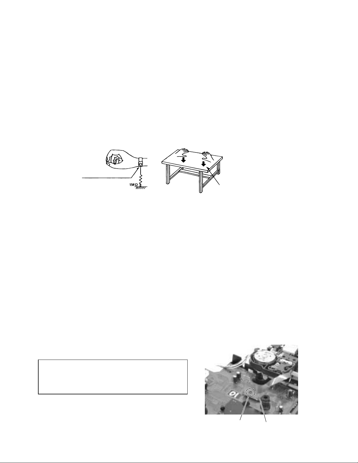
Preventing static electricity
1.Grounding to prevent damage by static electricity
Electrostatic discharge (ESD), which occurs when static electricity stored in the body, fabric, etc. is discharged,
can destroy the laser diode in the traverse unit (optical pickup). Take care to prevent this when performing repairs.
2.About the earth processing for the destruction prevention by static electricity
Static electricity in the work area can destroy the optical pickup (laser diode) in devices such as CD players.
Be careful to use proper grounding in the area where repairs are being performed.
2-1 Ground the workbench
Ground the workbench by laying conductive material (such as a conductive sheet) or an iron plate over
it before placing the traverse unit (optical pickup) on it.
2-2 Ground yourself
Use an anti-static wrist strap to release any static electricity built up in your body.
(caption)
Anti-static wrist strap
Conductive material
(conductive sheet) or iron plate
3. Handling the optical pickup
1. In order to maintain quality during transport and before installation, both sides of the laser diode on the
replacement optical pickup are shorted. After replacement, return the shorted parts to their original condition.
(Refer to the text.)
2. Do not use a tester to check the condition of the laser diode in the optical pickup. The tester's internal power
source can easily destroy the laser diode.
4.Handling the traverse unit (optical pickup)
1. Do not subject the traverse unit (optical pickup) to strong shocks, as it is a sensitive, complex unit.
2. Cut off the shorted part of the flexible cable using nippers, etc. after replacing the optical pickup. For specific
details, refer to the replacement procedure in the text. Remove the anti-static pin when replacing the traverse
unit. Be careful not to take too long a time when attaching it to the connector.
3. Handle the flexible cable carefully as it may break when subjected to strong force.
4. It is not possible to adjust the semi-fixed resistor that adjusts the laser power. Do not turn it
1-4
CAUTION:
Prior to disconnecting the flexible wire
extending from the pickup, solder it to the
short circuit land to prevent damage to the
pickup.
Short circuit land
CN611
Page 5
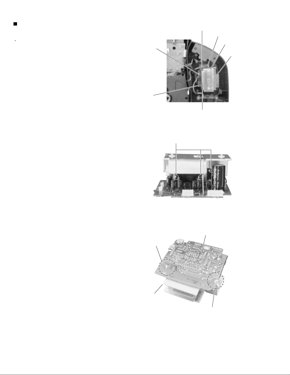
RS-WP1WT
Disassembly method
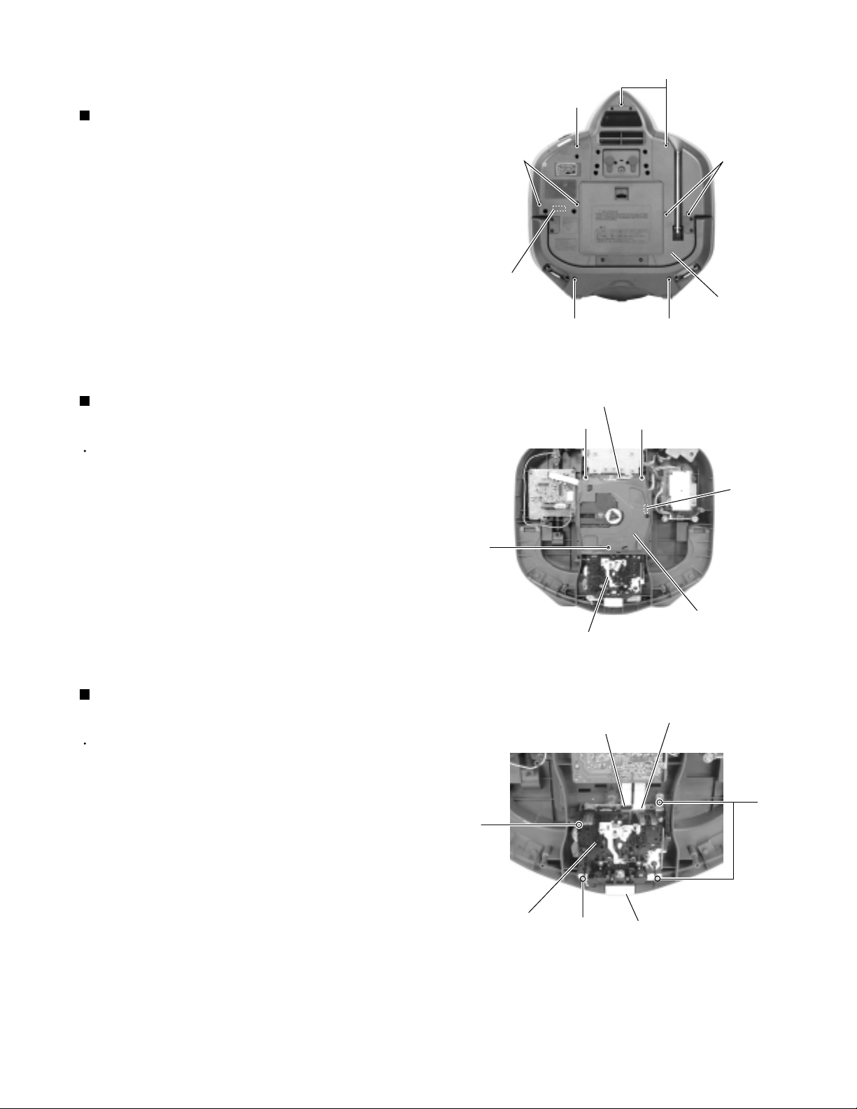
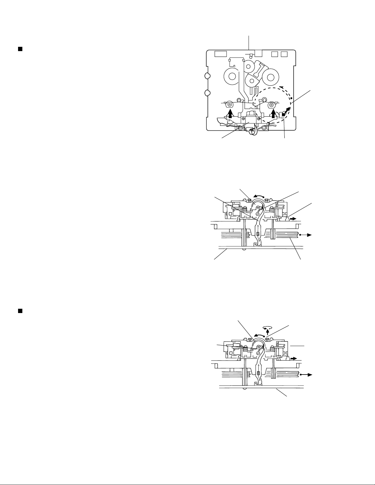
Removing the front panel assembly /
rear panel assembly (See Fig.1)
1.
Remove the nine screws A attaching the rear panel
assembly on the back of the body.
2.
Pull out the front panel assembly and the rear panel
assembly. Disconnect the speaker terminal on the
front side and connector CN112 on the connection
board on the rear side at the same time.
Removing the CD mechanism assembly
section (See Fig.2)
Prior to performing the following procedures, remove
the rear panel assembly.
1.
Disconnect the card wire from connector CN614 and
the wire from CN624 on the CD mechanism
assembly respectively.
2.
Remove the three screws B attaching the CD
mechanism assembly section.
A
Connection board
CN112
B
A
A
A
Rear panel
assembly
AA
Fig.1
CN624
BB
CN614
Removing the cassette mechanism
assembly (See Fig.3)
Prior to performing the following procedures, remove
the rear panel assembly and the CD mechanism
assembly section.
1.
Disconnect the card wire from connector CN33,
CN34 on the cassette mechanism assembly.
2.
Remove the four screws C and the cassette
mechanism assembly with the wire cover.
Cassette mechanism assembly
C
Cassette mechanism
assembly
C
Fig.2
CN33
Fig.3
CD mechanism
assembly section
CN34
C
Wire cover
1-5
Page 6
RS-WP1WT
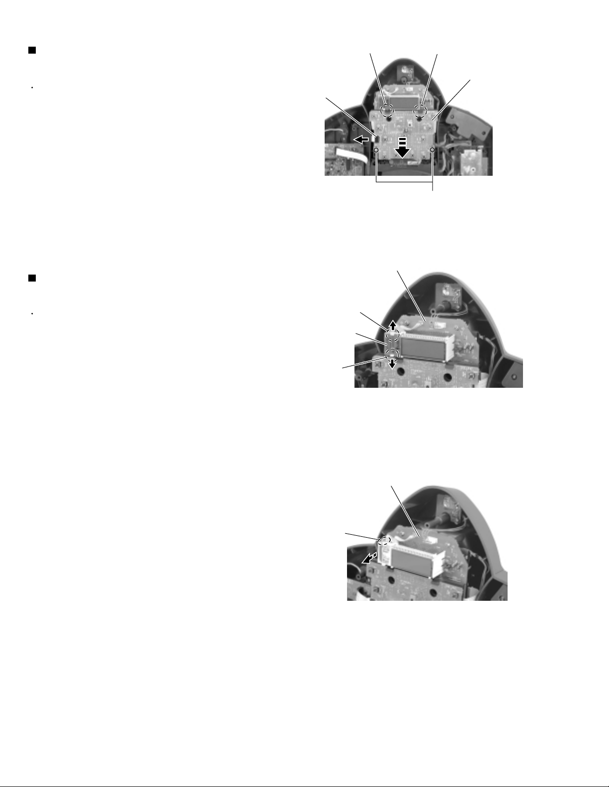
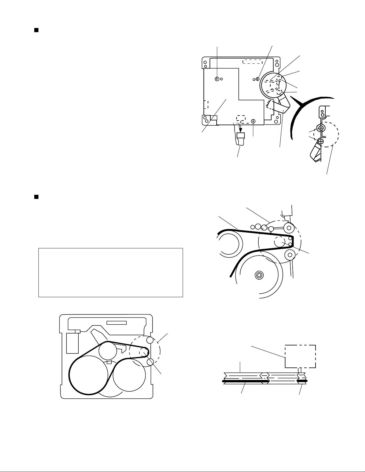
Removing the function switch board
(See Fig.4)
Prior to performing the following procedures, remove
the rear panel assembly.
1.
Disconnect the card wire from connector CN921 on
the function switch board.
2.
Remove the two screws D and move the function
switch board in the direction of the arrow to
disengage the two joints a.
Removing the LCD spare board / LED
board (See Fig.5 and 6)
Prior to performing the following procedures, remove
the rear panel assembly.
CN921
Joint hook b
LCD spare board
Joint a
LCD board
Joint a
Function switch board
D
Fig.4
1.
Remove the LCD spare board while pulling each
joint hook b outward.
2.
Pull out the LED board.
If necessary, unsolder FW925 soldering the wire on
the LED board.
Joint hook b
Fig.5
LCD board
LED board
FW925
Fig.6
1-6
Page 7
RS-WP1WT
Removing the LCD board
(See Fig.7 and 8)
Prior to performing the following procedures, remove
the rear panel assembly and the function switch
board.
1.
Remove the four screws E attaching the bracket.
2.
Disconnect the card wire from connector CN421,
CN422 and the wire from CN913 on the LCD board
respectively.
3.
Disconnect the wire from connector CN624 on the
CD mechanism assembly.
4.
Remove the two screws F attaching the LCD board
(The LCD spare board and the LED board are still
attached to the LCD board).
Removing the headphone jack board
(See Fig.9 and 10)
Prior to performing the following procedures, remove
the rear panel assembly.
LCD board
E
LCD board
CN913
F
E
Bracket
Fig.7
F
CN421
1.
Remove the two screws G attaching the headphone
jack board bracket.
2.
Pull out the headphone jack board bracket and the
headphone cover at the same time.
3.
Remove the two screws H attaching the headphone
jack board.
4.
Disconnect the wire from connector CN711 on the
headphone jack board.
H
CN422
CN624
Fig.8
G
Headphone cover
G
Headphone jack board
CN711
Fig.10
Headphone jack bracket
Fig.9
1-7
Page 8

RS-WP1WT
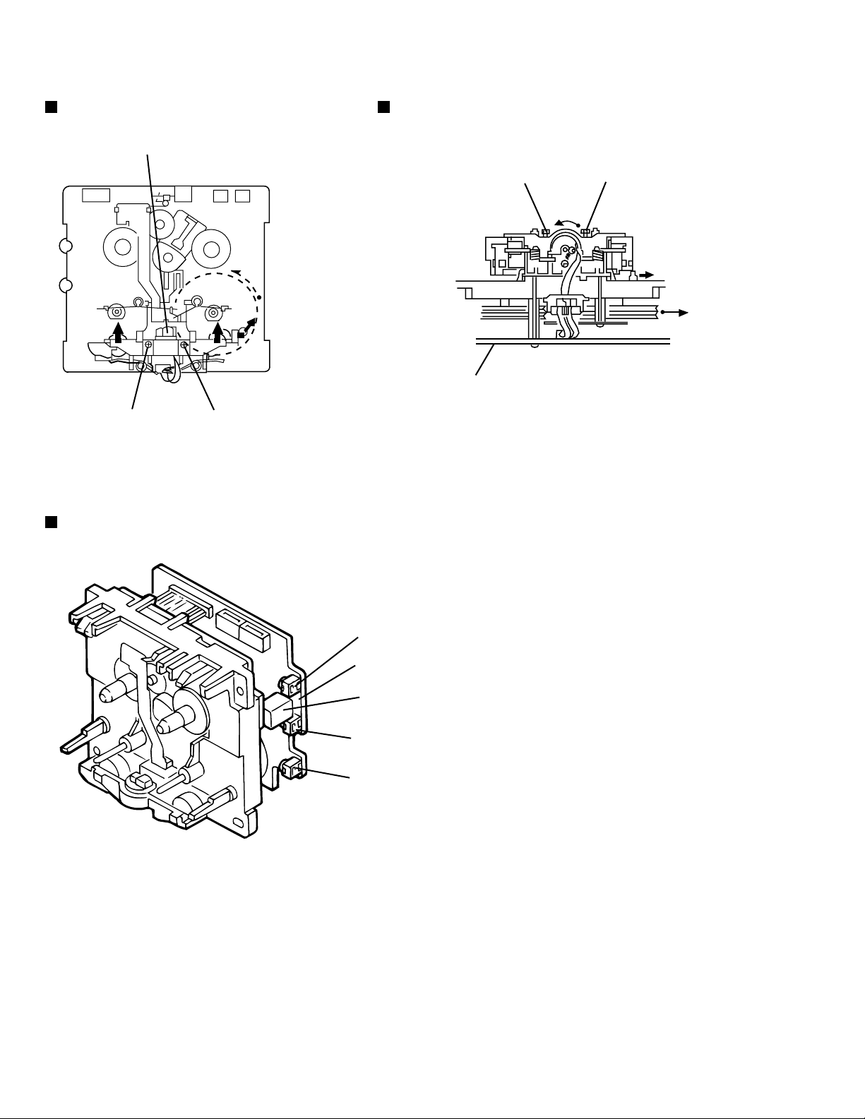
Removing the main board / sub (1) board
/ sub (2) board (See Fig.11 to 13)
Prior to performing the following procedures, remove
the rear panel assembly, the CD mechanism
assembly section and the LCD board.
1.
Remove the two screws J attaching the main board
on the back of the rear panel assembly.
2.
Disconnect the card wire from connector CN43 and
CN44 on the main board on the inside of the rear
panel assembly.
3.
Disconnect the wire from connector CN101 and
CN103 on the power board.
4.
Disconnect the wire from connector CN401 on the
battery board.
5.
Remove the six screws K attaching the main board.
Disconnect the card wire from connector CN91 on
the reverse side of the main board.
6.
Remove the screw L and disconnect the sub (1)
board from connector CN341 on the main board.
K
Rear panel assembly
J
Fig.11
Main board
K
CN103
CN101
7.
Disconnect the sub (2) board from connector CN371
on the main board.
Main board
CN91
K
CN43
CN341
CN371
CN44
Fig.12
Fig.13
K
Battery board
L
Sub (1) board
Sub (2) board
Power board
CN401
1-8
Page 9
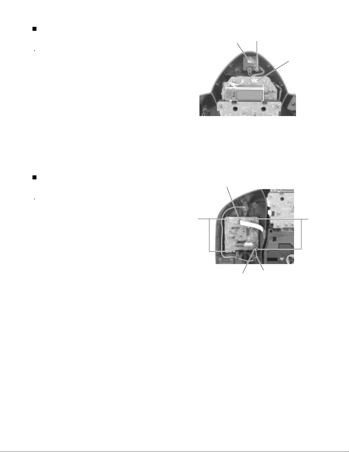
Removing the remocon board
(See Fig.14)
Remocon board
RS-WP1WT
M
Prior to performing the following procedure, remove
the rear panel assembly.
1.
Remove the screw M attaching the remocon board
and disconnect the wire from connector CN913 on
the LCD board.
Removing the tuner board (See Fig.15)
Prior to performing the following procedures, remove
the rear panel assembly.
LCD board
CN913
Fig.14
Tuner board
CN1
1.
Disconnect the card wire from connector CN1 and
the antenna wire from TP1 on the tuner board
respectively.
2.
Remove the four screws N attaching the tuner
board.
N
TP1
Fig.15
N
Antenna wire
1-9
Page 10
RS-WP1WT
Removing the power board
(See Fig.16 to 18)
Prior to performing the following procedures, remove
the rear panel assembly.
1.
Disconnect the wire from connector CN101, CN102
and CN103 on the power board.
2.
Remove the four screws O attaching the power
board.
3.
Remove the three screws O’ attaching the heat sink.
4.
Disengage the two joints c and remove the heat sink
from the power board.
O
CN103
O
CN102
Power board
CN101
O
Fig.16
O’
Joint c
Heat sink
Fig.17
Power board
Joint c
Fig.18
1-10
Page 11
Removing the connection board
(See Fig.19)
Prior to performing the following procedures, remove
the rear panel assembly.
1.
Disconnect the wire from connector CN102 on the
power board.
2.
Remove the two screws P and pull out the
connection board.
RS-WP1WT
P
Removing the battery board (1) / battery
board (2) (See Fig.20 and 21)
Prior to performing the following procedures, remove
the rear panel assembly.
1.
Remove the battery cover on the back of the rear
panel assembly.
2.
Remove the two screws Q retaining the battery
board (1).
3.
Pull out the battery board (1) and disconnect the wire
from inner connector CN401.
4.
Remove the two screws R and pull out the battery
board (2).
P
Fig.19
Fig.20
Connection board
CN112
Battery cover
Battery board (1)
Q
CN401
Fig.21
Battery board (2)
R
1-11
Page 12
RS-WP1WT
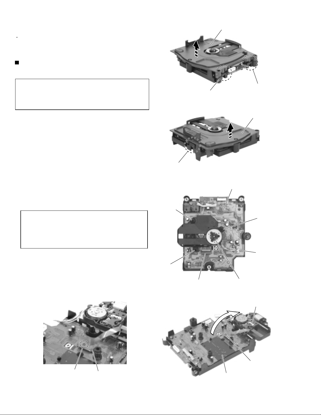
<CD mechanism assembly section>
Prior to performing the following procedures, remove
the rear panel assembly and the CD mechanism
assembly section.
Removing the CD mechanism assembly
(See Fig.22 to 26)
CAUTION:
1.
Release the three joint hooks d retaining the CD
mechanism cover.
2.
Disconnect the wire from connector CN612 on the
CD servo board.
3.
Remove the CD mechanism assembly from the three
dampers.
4.
Solder the flexible wire connected to connector
CN611 on the CD servo board to the short circuit
land under the flexible wire.
After soldering, disconnect the pickup wire from
connector CN611.
CAUTION:
Prior to disconnecting the flexible wire
extending from the pickup, solder it to the
short circuit land to prevent damage to the
pickup.
When reassembling, connect the pickup
wire extending from the pickup to
connector CN611 on the CD servo
board. Then unsolder the wire soldered
to the short circuit land.
CD mechanism cover
Joint hook d
Joint hook d
Fig.22
CD mechanism cover
Joint hook d
Fig.23
CD servo board
Damper
Damper
1-12
Short circuit land
CN611
Damper
CN611
CN612
CD servo assembly
Fig.24
CD mechanism assembly
(Pickup)
Pickup wire
(Short circuit land)
CD mechanism board
Fig.25Fig.26
Page 13
Removing the CD servo board
(See Fig.27)
Prior to performing the following procedure, remove
the CD servo assembly.
1.
Remove the four screws S retaining the CD servo
board.
2.
Unsolder FW616 where the wire extending from the
OPEN / CLOSE switch board is soldered.
Removing the OPEN / CLOSE switch
board (See Fig.27)
Prior to performing the following procedure, remove
the CD mechanism cover.
1.
Remove the screw T retaining the OPEN / CLOSE
switch board.
2.
Unsolder FW626 where the wire extending from the
CD mechanism board is soldered.
FW626
T
OPEN / CLOSE
switch board
S
FW616
S
CD mechanism board
Fig.27
RS-WP1WT
S
S
<Front assembly>
Removing the speaker assembly (R) and
(L) (See Fig.28)
Prior to performing the following procedure, remove
the front assembly.
1.
Remove the four screws U attaching the speaker
assembly (R).
2.
Remove the four screws V attaching the speaker
assembly (L).
3.
Remove the screw W attaching the speaker terminal.
If necessary, disconnect the wire from each speaker
terminal.
Removing the sub speaker assembly (R)
and (L) (See Fig.28)
Prior to performing the following procedure, remove
the front assembly.
1.
Remove the four screws X attaching the sub speaker
assembly (R).
Sub speaker assembly (R)
X
W
Speaker
terminal
U
Speaker assembly (R)
X
U
Fig.28
Sub speaker assembly (L)
Y
Y
V
Speaker assembly (L)
V
2.
Remove the four screws Y attaching the sub speaker
assembly (L).
If necessary, disconnect the wire from each speaker
terminal.
1-13
Page 14
RS-WP1WT
<Cassette mechanism section>
Removing the playback / recording &
eraser head (See Fig. 1 to 3)
1.
While shifting the trigger arms seen on the right side
of the head mount in the arrow direction, turn the
flywheel R in counterclockwise direction until the
head mount has gone out with a click (See Fig. 1).
2.
When the flywheel R is rotated in counterclockwise
direction, the playback / recording & eraser head will
be turned in counterclockwise direction from the
position in Fig. 2 to that in Fig. 3.
3.
At this position, disconnect the flexible P.C. board
(outgoing from the playback / recording & eraser
head) from the connector CN31 on the head
amplifier & mechanism control P.C. board.
4.
Remove the flexible P.C. board from the chassis
base.
5.
Remove the spring 1 from behind the playback /
recording & eraser head.
Flexible
board
Cassette mechanism
Trigger armHead mount
Fig. 1
Playback / Recording &
eraser head
Flywheel R
Spring 1
Trigger arm
6.
Loosen the reversing azimuth screw retaining the
playback / recording & eraser head.
7.
Take out the playback / recording & eraser head from
the front of the head mount.
8.
The playback / recoring & eraser head should also
be removed similarly according to steps 1 to 7 above.
Reassembling the playback / recording &
eraser head (See Fig.3)
1.
Reassemble the playback head from the front of the
head mount to the position as shown in Fig. 3.
2.
Fix the reversing azimuth screw.
3.
Set the spring 1 from behind the playback / recording
& eraser head.
4.
Attach the flexible P.C. board to the chassis base, as
shown in Fig. 3.
5.
The playback / recording & eraser head should also
be reassembled similarly to step 1 to 4 above.
CN31
Head amplifier & mechanism
control P.C. board
Fig. 2
Playback / Recording &
eraser head
Spring 1
Fig. 3
Flywheel R
Reversing azimuth
screw
Head
mount
Flexible
board
Head amplifier &
mechanism control
P.C. board
1-14
Page 15
Removing the head amplifier & mechanism
control board (See Fig. 4)
1.
Remove the cassette mechanism assembly.
2.
Disconnet the flexible wire from connctor CN31 to
the flexible board.
3.
After turning over the cassette mechanism assembly,
remove the three screws A retaining the head
amplifier & mechanism control board.
4.
Disconnect the connector CN32 on the board
including the connector CN 1 on the reel pulse P.C.
board.
5.
When necessary, remove the 4 pin parallel wire
soldered to the main motor.
A
Head amplifier &
mechanism control
board
Flexible board
CN31
CN32
A
4pin parallel wire
Fig. 4
RS-WP1WT
A
Belt
Main motor
assembly
B
B
Main
motor
assembly
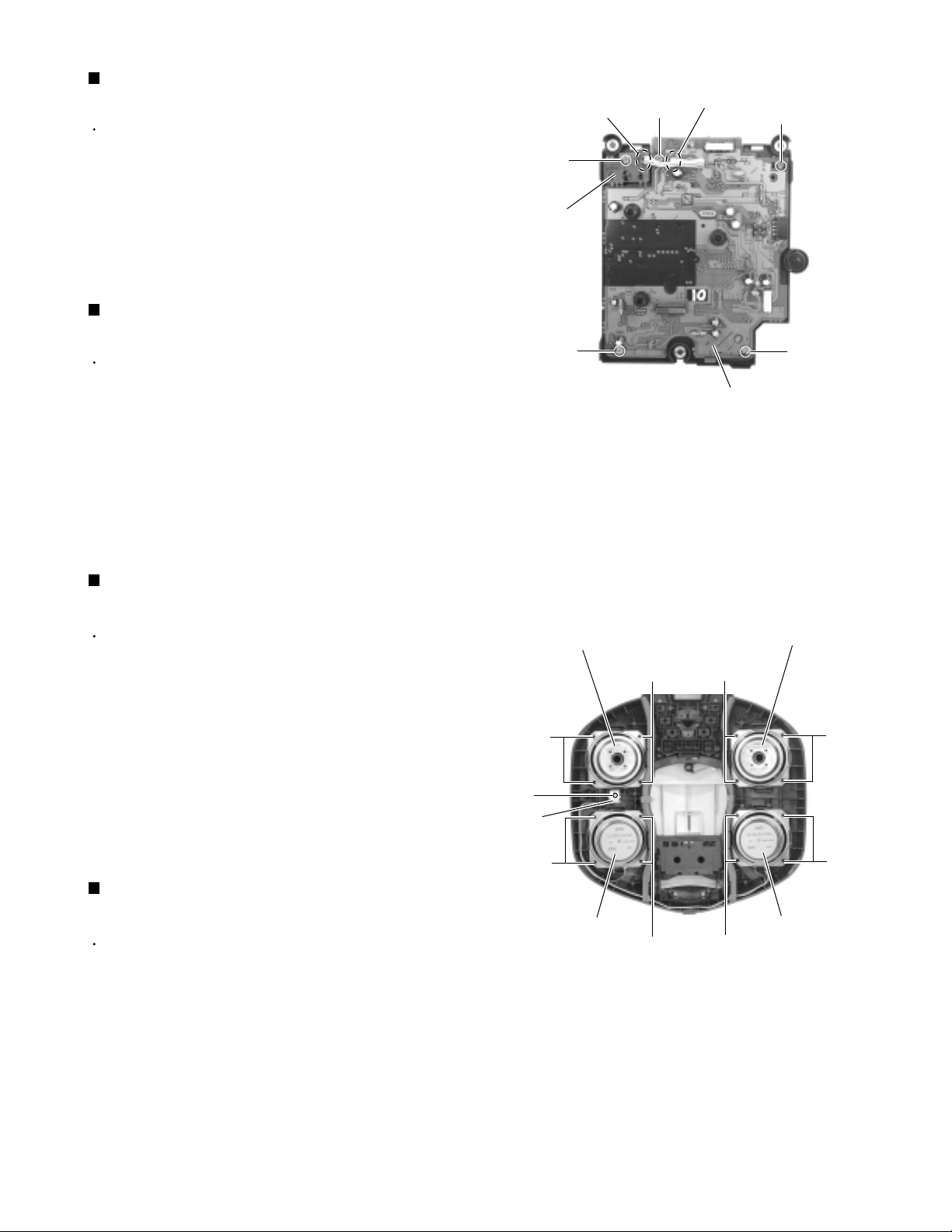
Removing the main motor assembly
1.
Remove the two screws B retaining the main motor
assembly (See Fig. 4 and 4a).
2.
While raising the main motor, remove the capstan
belt from the motor pulley (See Fig. 4a).
CAUTION:
Capstan
belt
Be sure to handle the capstan belt so
carefully that this belt will not be stained
by grease and other foreign matter.
Moreover, this belt should be hanged
while referring to the capstan belt
hanging method in Fig. 5 and 6.
Mechanism motor
assembly
Motor
pulley
Main motor
assembly
Capstan belt
Motor
pulley
Fig. 4a
Main motor
assembly
Flywheel
Fig. 5
Motor pulleyCapstan belt
Fig. 6
1-15
Page 16
RS-WP1WT
Removing the flywheel (See Fig. 7 and 8)
1.
Remove the head amplifier & mechanism control P.C.
board.
2.
Remove the main motor assembly.
3.
After turning over the cassette mechanism, remove
the two slit washers 1 and fixing the capstan shafts R
and L, and pull out the flywheel R and L respectively
from behind the cassette mechanism.
Flywheel R Flywheel L
Capstan shaft R Capstan shaft L
Flywheel R Flywheel L
Fig. 8
Removing the mecha braket reel pulse
P.C. board and solenoid (See Fig. 9 and
10)
1.
Remove the screw C attaching the mecha braket
assembly on the cassette assembly.
2.
Remove the screw D attaching the reel pulse board.
3.
Remove the five pawls a to e reattaining the reel
pulse board.
4.
From the surface of the reel pulse board parts,
remove the two pawls f and g retaining the solenoid.
Slit
washer 1
Fig. 7
Mecha braket assembly
Fig. 9
Slit
washer 1
C
1-16
Solenoid
Reel pulse board
a b c d e
g
f
Fig.10
D
Page 17

Adjustment method
RS-WP1WT
Measuring devices necessary for adjustment
1. Low-frequency oscillator
It must have the ability to output 600ohm from 0 dBs
at an oscillation frequency of 20 Hz-50 Hz.
2.Attenuator impedance: 600ohm
3.Electronic voltmeter
Tuner section
Voltage input to the tuner .......................... +B: DC 5.7 V
VT: DC 12 V
Standard measuring output ....... 26.1 mV (0.28 V)/3ohm
Input locations ..................... AM: standard loop antenna
FM: TP1 (hot) and TP2 (GND)
Standard settings for measuring volume
4.Distortion meter
5.Frequency counter
6.Wow and flutter meter
7.Test tapes
VT-712: tape speed and rotational distortion (3 kHz)
VT-724: standard level (1 kHz)
VT-703: head angle adjustment (10 kHz),
or use VT-73
VT-739: reproduction of frequency characteristics
(1 kHz, 63 Hz, 10 kHz)
8.Blank tape
Type I : AC-225 (TDK-AD)
Type II : AC-514 (TDK-SA)
9.Torque gauge: Tension gauge for playback,
fast-forward and rewind.
FWD (TW211A), REW (TW212A)
and FF/REW (TW2231A)
Sound ..................................................................... OFF
Effective hyper bass ............................................... OFF
Volume adjustment ........................................... VOL. 23
Precautions for measuring
1.Input 30 pF and 33 kohm to the IF sweeper output
2.Lower the output level of the IF sweeper as much as
3.The IF sweeper needs no adjustment as it is a fixed
4.It is not necessary to perform any kind of adjustment
and 0.082 F and 100 kohm to the sweeper input,
respectively.
possible in the adjustable range.
component.
on the MPX, as a ceramic oscillator is used for
measuring.
Specifications for measurement
Power supply voltage ................... AC 230 V (50 Hz)
Standard output ........................ Speaker: 0.775V/4ohm
Headphone:0.245V/32ohm
Standard frequency and input level
................... 1 kHz: AUX: -8 dBs
Input level for reproduction of recording characteristics
................... AUX: -28 dBs
Measuring output terminal ................... Speaker: CN112
Load resistance .................................................... 4ohm
Radio input signal
AM frequency ..................................................... 400 Hz
Degree of modulation in AM band .......................... 30%
FM frequency ...................................................... 400 Hz
Frequency deviation in FM band ..................... 22.5 kHz
5.FM tracking adjustment is not necessary as a fixed
coil is used.
6.The grounding circuit is separate from the input and
output. Therefore, be sure to connect to ground
carefully when measuring both the input and output
voltages simultaneously using 2 channels of the
electronic voltmeter.
7.The speaker's minus terminal cannot be connected to
ground when using a BTL format amplifier. Therefore,
do not connect any type of ground wire to this
terminal. The OTL format is used with this system.
8.Use a large wire to connect to the dummy impedance
generator when measuring the output.
9.Be sure to use a band pass filter (DV-12) when using
mixed tape.
1-17
Page 18
RS-WP1WT
Location of parts to be adjusted
Cassette handling mechanism Cassette handling mechanism (reverse side)
Head for recording, playing
and erasing the tape
Head azimuth
adjusting screw (fast-forward)
Head azimuth adjusting
screw (rewind)
Head azimuth adjusting
screw (fast-forward)
CN31
Head for recording,
playing and erasing the tape
Head azimuth adjusting
screw (rewind)
Location of parts to be adjusted
VR37
Motor speed
TP
Bias oscillation frequency (wide pattern)
L301
Bias oscillation frequency
VR31
Lch recording frequency (bias adjustment)
VR32
Rch recording frequency (bias adjustment)
1-18
Page 19
Adjustment of cassette handling mechanism
RS-WP1WT
Items Condition Method for adjustment
Confirmation
of head angle
Confirmation
of tape speed
Test tape: VT-703 (10 kHz)
Measuring output terminal:
Speaker terminal, speaker (R)
(Load resistance: 4ohm),
headphone terminal
Test tape: VT-712 (3 kHz)
Measuring output terminal:
Headphone terminal
(1) Play back the VT-703 test tape.
(2) Adjust the head azimuth screws so
that the tape playback mechanism
records the maximum output level in
both the fast-forward and rewind
direction.
(3) In all cases, both the fast-forward and
rewind direction should be adjusted
using head azimuth screws.
Adjust VR37 so that the frequency
counter records 3,015 Hz 15 Hz when
playing back the end of the VT-712 test
tape (3 kHz) in the fast-forward direction.
and confirmation
Items to be confirmed and standard values
Items Condition Method for adjustment
Difference in
speed
between fastforward and
rewind
Test tape: VT-712 (3 kHz)
Measuring output terminal:
Speaker terminal, speaker (R)
(Load resistance: 4 ),
headphone terminal
The difference between fast-forward and
rewind should be less than 60 Hz on the
frequency counter when playing back the
beginning of the VT-712 test tape (3 kHz)
in both directions.
and confirmation
Standard
value
Maximum
output
Tape speed
of cassette
deck: 3,015
Hz 15 Hz
Standard
value
Less than 60 HzShould be
Parts to be
adjusted
Adjust the
head
azimuth
screws
when
changing
the head.
VR37
Parts to be
adjusted
confirmed
when
changing
the motor.
Wow and
flutter
Test tape: VT-712 (3 kHz)
Measuring output terminal:
Headphone terminal
Wow and flutter should be recorded at
less than 0.25% (WRMS) when playing
back the VT-712 test tape (3 kHz) in the
fast-forward direction.
Electronic performance
Items Condition Method for adjustment
Confirmation
of output
Confirmation
of
reproduction
of frequency
characteristic
s
Recording
bias
frequency
Measuring output terminal:
CN34-5 or 7-terminal
preamp base
Test tape: VT-724
Measuring output terminal:
Headphone terminal
Test tape: VT-739
Fast-forward or rewind
direction:
Test tape: TYPE II (AC-
514)
Measuring terminal: Bias
TP on the base
Confirm that the output from the CN34-5
or 7-terminal preamp base connector is 25 dBs 3 dB when playing back the VT724 test tape.
Reference value: The output from the
headphone terminal is -7 dB 4 dB.
Confirm that the 10 kHz reproduction
level is -1 dB 5 dB compared to the 1
kHz reproduction level when playing back
the VT-739 test tape.
Switch the bias (beat cut switch) between
1 and 2 to confirm that the frequency
changes. Load the test tape (AC-514 for
TYPE II) into the mechanism and preset
it to the record-pause mode.
Confirm that the bias TP frequency on
the base is 100 kHz 6kHz.
and confirmation
Less than
0.25%
(WRMS)
Standard
value
Output of CN345 terminal: -25
dBs 3 dB
Difference
between Lch
and Rch: within
3 dB
Difference
between 10
kHz and 1 kHz
should be -1
dB 5 dB.
100 kHz 6 kHz
Parts to be
adjusted
1-19
Page 20

RS-WP1WT
Standard values for confirmation of electronic performance
Items Condition Method for adjustment
and confirmation
Erasing
current
(standard
and
reference
value)
Adjustment of
reproduction
of frequency
characteristic
s
Fast-forward and
rewind direction:
Recording mode
AC-514 for TYPE II,
AC-225 for TYPE I
Measuring terminal:
Both erase head terminals
Standard frequencies:
1 kHz and 10 kHz
(REF: -20 dB)
Test tape: TYPE II:
AC-514
Measuring input
terminal: OSC IN
Load the test tape (AC-514 for TYPE II,
AC-225 for TYPE I) into the tape
playback mechanism and preset it to the
record-pause mode.
After setting it to the recording mode,
send 1 M in series to the erase head and
measure the erasing current from both
erase head terminals.
Load the test tape (AC-514 for TYPE II,
AC-225 for TYPE I) into the tape
playback mechanism and preset it to the
record-pause mode.
Input the standard value of -20 dB and
the standard frequencies of 1 kHz and 10
kHz repeatedly to the microphone input
from the transmitter in the recording
mode. Adjust VR31 for Lch and VR32 for
Rch so that the difference in level
between 10kHz and 1 kHz is -1dB 5dB.
Repeat the above for TYPE I and confirm
that the difference in level is -XdB dB.
Standard
value
TYPE II: 110
mA
TYPE I: 75 mA
Difference in
output
between 1 kHz
and 10 kHz: -1
dB 5 dB
Parts to be
adjusted
Lch: VR31
Rch: VR32
1-20
Page 21
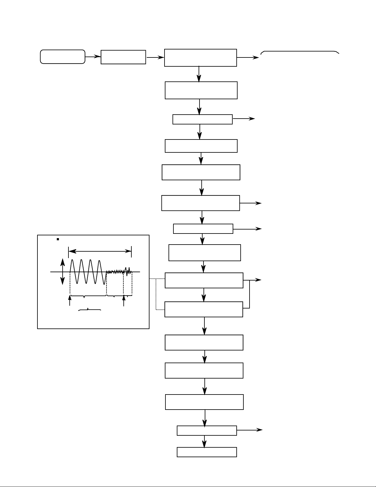
Flow of functional operation until TOC read
Power ON
Play Key
Slider turns REST
SW ON.
Automatic tuning
of TE offset
Confirm that the voltage at the pin3
of CN612 is "H"\"L"\"H".
RS-WP1WT
Check Point
Tracking error waveform at TOC reading
Approx.3sec
Tracking
servo
off states
Automatic measurement
of TE amplitude and
automatic tuning of
TE balance
VREF
pin 33 of
IC601(TE)
Approx
1.8V
Disc states
to rotate
Tracking
servo
on states
Disc to be
braked to stop
TOC reading
finishes
500mv/div
2ms/div
Fig.1
Laser ON
Detection of disc
Automatic tuning of
Focus offset
Automatic measurement of
Focus S-curve amplitude
Disc is rotated
Focus servo ON
(Tracking servo ON)
Automatic measurement of
Tracking error amplitude
Automatic tuning of
Tracking error balance
Check that the voltage at the
pin18 of IC604 is + 5V?
Confirm that the Focus error
S-cuve signal at the pin32 of
IC601 is approx.2Vp-p
Confirm that the signal from
pin24 IC603 is 0V as a
accelerated pulse during
approx.400ms.
Confirm the waveform of
the Tracking error signal.
at the pin 33 of IC601 (R6401)
(See fig-1)
Automatic tuning of
Focus error balance
Automatic tuning of
Focus error gain
Automatic tuning of
Tracking error gain
TOC reading
Play a disc
Confirm the eye-pattern
at the lead of TS601
1-21
Page 22

RS-WP1WT
Maintenance of laser pickup
(1) Cleaning the pick up lens
Before you replace the pick up, please try to
clean the lens with a alcohol soaked cotton
swab.
(2) Life of the laser diode
When the life of the laser diode has expired,
the following symptoms will appear.
1. The level of RF output (EFM output : ampli tude of eye pattern) will below.
Is the level of
RFOUT under
1.25V 0.22Vp-p?
YES
O.K
NO
Replace it.
Replacement of laser pickup
Turn off the power switch and, disconnect the
power cord from the ac outlet.
Replace the pickup with a normal one. (Refer
to "Pickup Removal" on the previous page)
Plug the power cord in, and turn the power on.
At this time, check that the laser emits for
about 3 seconds and the objective lens moves
up and down.
Note: Do not observe the laser beam directly.
Play a disc.
Check the eye-pattern at TS601.
Finish.
(3) Semi-fixed resistor on the APC PC board
The semi-fixed resistor on the APC printed circuit board which is attached to the pickup is used to adjust the laser
power. Since this adjustment should be performed to match the characteristics of the whole optical block, do not
touch the semi-fixed resistor.
If the laser power is lower than the specified value, the laser diode is almost worn out, and the laser pickup should
be replaced.
If the semi-fixed resistor is adjusted while the pickup is functioning normally, the laser pickup may be damaged
due to excessive current.
1-22
Page 23

Description of major ICs
LA4905 (IC101) : Power amp IC
1. Terminal layout
123
RS-WP1WT
2. Block diagram
STBY
D.C
PRE GND
IN 1
21
20
2
3
Standby SW
Ripple
filter
Input amplifier
Vcc Vcc(SW)
10
Switching
regulator block
H.L.S.
ABCD
H.L.S. :
Higher
Level signal
selector
Nonlinear/output stage
CH 1
11
Amplifier output stage
SW
drive
8
9
SW B
15
SW E
14
SW OUT1
12
SW OUT2
13
SW GND
16
A
+OUT 1
7
PWR GND 1
5
B
BEEP
IN 2
ON TIME
4
1
23
BEEP
amplifier
Input amplifier
ON MUTE
muting circuit
Power supply/ground shorting
protection circuit
Overvoltage/thermal protection
circuit
CH 2
Nonlinear amplifier/output stage
Pop noise
prevention circuit
-OUT 1
6
C
D
18
19
17
22
-OUT 2
PWR GND 2
+OUT 2
N.C.
1-23
Page 24

RS-WP1WT
BA15218F-XE (IC201, IC701) : Dual operation amplifier
1. Terminal layout
OUT1 1
-IN1 2
+IN1 3
VEE 4
2. Block diagram
Vcc
-IN
+IN
1
2
R1
Q5
Q1
Q2
D1
Q3 Q4
8 Vcc
7 OUT2
6 -IN2
5 +IN2
C2
Q9
R5
Q6
Q8
Q10
Q7
R7
Q11
R6
Q12
R8
Q18Q13
OTHER
CH
Q19
Q17Q16
C1
R3R2
R4
VEE
OUTPUT
GP1U281X (IC801, IC802) : Receiver for remote controller
+
–
Amp.
Limiter Integrator Comparator
B.P.F
Demodulator
GND
Q14 Q15Q114
VCC Vout
R9
123
1-24
Page 25

KIA78R06PI(IC381) US 6V
1. Terminal layout 2. Block diagram
V
1
IN
RS-WP1WT
1V
0
+
OUTPUT ON/OFF
4123
2
Control
CONTROL
KIA78R08PI(IC301) SW 8V REGULATOR
1. Terminal layout 2. Block diagram
V
1
IN
BANDGAP
REFERENCE
ASD
PROTECTION
OVERHEAT
PROTECTION
2
GND
1V
0
+
BANDGAP
REFERENCE
OUTPUT ON/OFF
4123
2
Control
CONTROL
ASD
PROTECTION
OVERHEAT
PROTECTION
2
GND
1-25
Page 26

RS-WP1WT
LC72136N (IC2) : PLL frequency synthesizer
1. Terminal layout
1
XT
CE
DI
DO
2
3
4
5
6
7
8
FM/AM
CLOCK
FM/ST/VCO
AM/FM
9
10
11
SDIN
2. Block diagram
22
21
20
19
18
17
16
15
14
13
12
XT
GND
LPFOUT
LPFIN
PD
VCC
FMIN
AMIN
IFCONT
IFIN
1
22
16
15
3
4
5
6
17
21
3. Pin function
Pin
Symbol
No.
1
2
3
4
5
6
7
8
9
10
11
XT
FM/AM
CE
DI
CLOCK
DO
FM/ST/VCO
AM/FM
LW
MW
SDIN
Reference
Driver
Swallow Counter
1/2
C
2
B
I/F
Powe r
on
Reset
Function
I/O
X'tal oscillator connect (75kHz)
I
LOW:FM mode
O
When data output/input for 4pin(input) and
I
Swallow Counter
1/16,1/17 4bit
1/16,1/17 4bit
12bit
Programmable
DriverS
Data Shift Register & Latch
7821113
6pin(output): H
Input for receive the serial data from
I
controller
Sync signal input use
I
Data output for Controller
O
Output port
"Low": MW mode
O
Open state after the power on reset
O
Input/output port
I/O
Input/output port
I/O
Data input/output
I/O
Phase
Detector
Charge Pump
Unlock
Detector
Universal
Counter
Pin
No.
12
IFCONT
13
14
15
16
17
18
19
LPFOUT
20
21
22
Symbol
IFIN
AMIN
FMIN
VCC
PD
LPFIN
GND
XT
18
19
20
12
I/O
Function
IF counter signal input
I
IF signal output
O
Not use
-
AM Local OSC signal output
I
FM Local OSC signal input
I
Power suplly(VDD=4.5-5.5V)
-
When power ON:Reset circuit move
PLL charge pump output(H: Local OSC
O
frequency Height than Reference frequency.
L: Low Agreement: Height impedance)
Input for active lowpassfilter of PLL
I
Output for active lowpassfilter of PLL
O
Connected to GND
-
X'tal oscillator(75KHz)
I
1-26
Page 27

LC75342 (IC501) : E. volume
1. Terminal layout
30 16~
115~
2. Block diagram
11
10
9 8 8 7 5
RS-WP1WT
12
13
14
15
16
17
18
19
20
CONTROL
CIRCUIT
LOGIC
CIRCUIT
CONTROL
CIRCUIT
3. Pin function
Pin
Symbol Symbol
No.
DI
1
2
3
4
5
6
7
8
VSS
TEST
LOUT
LBASS2
LBASS1
LTRE
Serial data and clock input for IC control
CE
Chip enable
GND
Electric volume connection for test
Volume control and equalizer input
Connection for resistor and capacitor that
from
the bass band filter
Connection for capacitor that from the
Function
treble band filter
LIN
9
10
11
12
13
14
15
16
LSEL0
Volume control and equalizer input
Input selector output
L4
Input signal connections
L3
Input signal connections
L2
Input signal connections
L1
Input signal connections
NC
Not used
NC
Not used
Pin
No.
17
18
19
20
21
22
23
24
25
26
27
28
29
30
CCB
INTERFACE
R1
R2
R3
R4
RSEL0
RIN
RTRE
RBASS1
RBASS2
ROUT
NC
Vref
VDD
CL
4
LVref
RVref
262524232221
3
2
1
30
29
28
27
Function
Input signal connections
Input signal connections
Input signal connections
Input signal connections
Input selector output
Volume control and equalizer input
Connection for capacitor that from the treble
band filter
Connection for resistor and capacitor that from
the bass band filter
Volume control and equalizer input
Not used
Connection to the 0.5X VDD voltage generator
circuit used as the analog signal ground
Power supply
Serial data and clock input for IC control
1-27
Page 28

RS-WP1WT
MN101C38CHX (IC901) : System controller
Pin No.
1~4
5~7
8
9,10
11
12,13
14
15
16
17
18
19
20
21
22
23
24
25
26
27
28
29
30
31
32
33
34
35
36
37
38
39
40
41
42
43
44
45
46
47
48
49
50
51
52
53
54
55
56
57
58~60
61
62
63
64
65~74
75~79
80~100
Symbol I/O Function
COM 3~0
VLC 3~1
VDD
OSC2,1
VSS
XI,XO
MMOD
VREF-
VER
REGSAFETY
CD5 SAFETY
CD3 SAFETY
TAPE0
KEY1
GND
MPX
VREF+
SO
SI
SCK
SCMD
S STAT
SCLK
PERIDO
RST
BEAT
SRST
VCE
V DATA
VCLK
REM
BUP
PIN
DC/BATT
HP JACK
SMUTE
BCTL
POUT
LLED
STBLED
LCLED
PLAY
REEL
LATCH
DOOR
READY
MIC JACK
A HB 1
A HB 2
PSWOFF
F. CD
F. T U
F. AU X
PBMUTE
GND
SEG0~20
O
I/O
I/O
O
O
O
O
O
O
O
O
O
O
O
O
O
O
O
FL grid control signal output
I
-
-
I
I
I
I
I
I
I
I
I
I
I
I
I
I
I
I
I
I
I
I
I
I
I
I
-
I
I
I
I
I
I
-
-
-
-
Power supply +5V
Oscillation terminal (8MHz)
Connect to GND
Sub clock (32.768kHz)
Connect to GND
Reference voltage (-)
Version select
Regulator safety detect
Regulator safety detect CD5
Regulator safety detect CD3
Tape input
Key input 1
Non connect
Stereo detect
Power supply +5V
Serial data output
Serial data input
Serial bus clock
Senal data bus
Status bus
Shift clock input
Chip enable signal output
Reset input
Beat cut sw
Reset signal for CD
Chip enable for VOL. IC
Volume data for VOL. IC
Volume clock for VOL. IC
Remocon signal input
Buck-up detect
Power key input
DC/Battery select input
HP jack select input
System mute output
Back-up power supply control output
Power on control output
Non connect
Stand by LED control output
Back light LED control output
Cassetle play sw dotection input
Cassetle reel palus detection input
Serial data latch output
Door open / close detection input
Serial data ready input
Mic jack in out detection
Artive Hyper Bass select output signal 1
Artive Hyper Bass select output signal 2
Power sw off detection
Non connect
Function for CD
Function for tuner
Non connect
Playback mute
Connect to GND
Non connect
FL segment signal output
1-28
Page 29

MN35530 (IC601) : Digital servo & processor
1. Terminal layout
20 1~
21
~
40
41 60
2. Pin function
Pin
Symbol
No.
1
DVD3V
2
D0
3
D1
4
NWE
5
NRAS
6
D2
7
D3
8
NCAS0
9
NCAS1
10
A8
11
A7
12
A6
13
A5
14
A4
15
A9
16
A0
17
A1
18
A2
19
A3
20
DVSS2
21
DVDD2
22
SPOUT
23
TRVF
24
TRVR
25
TRF
26
TRR
27
FOF
28
FOR
29
FBAL
30
TBAL
31
CSEL
32
FE
33
TE
RF ENV
34
OFT
35
NRFDET
36
BDD
37
LDON
38
ARF
39
IREF
40
80
~
61
~
I/O Function
Power supply
Data input
I
Data input
I
Write enable
I/O
Low address strove
I/O
Data input
I
Data input
I
Column address strove 0
I/O
Column address strove 1
I/O
Adress output
O
Adress output
O
Adress output
O
Adress output
O
Adress output
O
Adress output
O
Adress output
O
Adress output
O
Adress output
O
Adress output
O
Connect to GND
Power supply
Spindle control output
O
Traverse control output (F)
O
Traverse control output (R)
O
Tracking control output (F)
O
Tracking control output (R)
O
Focus control output (F)
O
Focus control output (R)
O
Focus balance adjust output
O
Trarcking balance adjust output
O
Chip select input
I
Focus error signal input (Analog input)
I
Tracking error signal input (Analog input)
I
RF envelope signal input (Analog input)
I
Off track signal input (H:off track)
I
RF signal input
I
BDO input pin (L:detect)
I
Laser ON signal output (H:on)
I
RF signal input
I
Reference current input
I
Pin
No.
41
42
43
44
45
46
47
48
49
50
51
52
53
54
55
56
57
58
59
60
61
62
63
64
65
66
67
68
69
70
71
72
73
74
75
76
77
78
79
80
Symbol
ADPVCC
DSLF
DRF
PLLF
VCOF
AVDD2
AVSS2
OUTL
AVSS2
OUTR
AVDD1
FSEL
TMOD1
TMOD2
FLAG
CVS
EXTO
EXT1
EXT2
TX
MCLK
M DATA
MLD
BLKCK
SQCK
SUBQ
DMUTE
S TAT
NRST
PC
PMCK
SMCK
SUBC
SUCK
NCLDCK
NTEST
X1
X2
DVDD1
DVSS1
I/O Function
Vcc for A/D input
I
Loop filter pin for DSL
I/O
Bias pin for DSL input
I
Loop filter pin for DSL
I/O
Vcc OFF input
I
Power supply
Connect to GND
Lch audio output
O
Connect to GND
Rch audio output
O
Power supply
FS selection input
I
Connect to GND
Connect to GND
Flag output signal
O
Non connect
NC
NC
NC
Digtal audio interface output
O
Micon command clock signal input
I
Micon command data input
I
Micon command load signal input
I
Sub-code block clock signal output
O
Outside clock for sub-code Q resistor input
O
Sub-code Q-code output
O
Digtal mute
O
Stetus signal input
I
Reset input
I
Power control input
I
Non connect
Serial Master clock input
I
Non connect
Clock input for sub code/serial output
I
NC
NC
Input of 33.8688MHz x'tal oscillation circuit
I
Out of x'tal oscillation circuit
O
Power supply
Connect to GND
-
RS-WP1WT
1-29
Page 30

RS-WP1WT
MN101C30AHY (IC602) : CD micon
1. Terminal layout
32 17-
33
-
48
49 64
2. Pin function
Pin
Symbol
No.
1
PA 3
2
PA 4
3
PA 5
4
PA 6
5
PA 7
6
VREF+
7
VDD
8
OSC2
9
OSC1
10
VSS
11
X1
12
X0
13
MMOD
14
SBOO
15
SUBQ
16
SQCK
17
S STAT
18
SCMD
19
SCLK
20
SREADY
21
RST
22
M-DATA
23
MLD
24
MCLK
25
S TAT
26
XRST
27
BLKCK
28
P21
29
P22
30
P23
31
P24
32
REST
16
-
1
-
I/O Function
-
Connect to GND
-
Connect to GND
-
Connect to GND
-
Connect to GND
-
Connect to GND
-
Reference Voltage
-
Power supply
O
X'tal OSC output terminal
I
X'tal OSC input terminal
-
Connect to GND
I
Connect to GND
O
Non connect
I
Connect to GND
-
NC
I
Sub-code Q-code output
Outside clock for sub-code Q resitor input
O
Statas signal output
O
Sireal data
I/O
Shift clock input
I
Start signal
O
Reset signal input
I
Micon command data signal input
I
Micon command load signal input
I
Micon command clock signal input
I
Status signal
O
Reset
O
Feed Kick control
I
Eanable signal
Connect to GND
Connect to GND
Connect to GND
-
I
Rest sw input
output
output
output
output
Pin
No.
33
34
35
36
37
38
39
40
41
42
43
44
45
46
47
48
49
50
51
52
53
54
55
56
57
58
59
60
61
62
63
64
Symbol
DOOR
O MUTE
DMUTE
PDOWN
AMUTE
P61
P62
P63
P64
P65
P66
P67
P70
P71
P72
P73
P74
P75
P76
P77
P87
P86
P85
P84
P83
P82
P81
ESPCHG
VREFKEY0
KEY1
PA 2
I/O Function
Door open/close sw detection input
I
Muting output
O
Digtal mute output
O
Power off detect input
I
Connect to GND
Connect to GND
Connect to GND
Connect to GND
Connect to GND
Connect to GND
Connect to GND
Connect to GND
Connect to GND
Connect to GND
Connect to GND
Connect to GND
Connect to GND
Connect to GND
Connect to GND
Connect to GND
Connect to GND
Connect to GND
Connect to GND
Connect to GND
Connect to GND
Connect to GND
Connect to GND
Connect to GND
Connect to GND
Connect to GND
Connect to GND
Connect to GND
-
1-30
Page 31

AN4801SB-W (IC603) : BTL DRIVER
1. Terminal layout 2. Block diagram
RS-WP1WT
1SPIN
2PC2
3TRVIN
4PC1
5RESET
6NC
7NC
8PGND1
9PVCC1
10TRV11TRV+
12SP+
13SP14T-
28 FIN2
27 FIN1
26 TRIN
25 FOIN
24 VREF
23 SVCC
22 NC
21 NC
20 STBY
19 PGND2
18 PVCC2
17 F+
16 F15 T+
3. Pin function
1
2
3
4
5
6
7
8
9
10
11
12
13
14
Symbol
SPIN
PC2
TRVIN
PC1
RESET
NC
NC
PGND1
PVCC1
TRVTRV+
SP+
SPT-
Pin No. Pin No.
I/O Function Symbol
I
Spindle servo control input
I
Power control
I
Traverse signal input
I
Power control
I
Reset signal input
-
Non connect
-
Non connect
-
Connect to GND
-
Power supply
-
Traverse drive output(-)
O
Traverse drive output(+)
O
Spindle servo drive output(-)
O
Spindle servo drive output(-)
O
Tracking servo signal output(-)
15
16
17
18
19
20
21
22
23
24
25
26
27
28
T+
FF+
PVCC2
PGND2
STBY
NC
NC
SVCC
VREF
FOIN
TRIN
FIN1
FIN2
I/O
O
Tracking servo signal output(+)
O
Focus servo signal output(-)
O
Focus servo signal output(+)
-
Power supply
-
Connect to GND
I
Stand-by input
-
Non connect
-
Non connect
I
Reference voltage input
I
Voltage reference input
I
Focus coil driver
I
Tracking coil driver input
-
GND
-
GND
Function
1-31
Page 32

RS-WP1WT
AN8838SB(IC604) : RF & Servo AMP
1. Terminal layout 2. Block diagram
1VCC
2POA
3POC
4POB
5POD
6RFFB
7RF
8RF IN
9LPD
10LD
11CSBRT
12CEA
13BDO
14GND
3. Pin function
Pin No.
1
2
3
4
5
6
7
8
9
10
11
12
13
14
15
16
17
18
19
20
21
22
23
24
25
26
27
28
28 PDF
27 PDE
26 VREF
25 TEOUT
24 TEN
23 TBAL
22 FBAL
21 FEN
20 FEOUT
19 ENV
18 LDON
17 OFTR
16 PDOWN
15 RFDET
Symbol I/O Descriptions
VCC
POA
POC
POB
PO
RFFB
RF
RF IN
LPD
LD
CSBRT
CEA
BDO
GND
RFDET
PDOWN
OFTR
LDON
ENV
FEOUT
FEN
FBAL
TBAL
TEN
TEOUT
VREF
PDE
PDF
O
O
I/O
O
O
O
O
O
O
O
I
I
I
I
I
I
I
I
I
I
I
I
I
I
I
I
Power supply
Focus signal input A
Focus signal input C
Focus signal input B
Focus signal input D
RFamp input
RFamp output
RF input
APC amp input terminal
APC amp output terminal
OFF Track External terminal
A capacitor is connected to this terminal detect the envelope of RF
signal
BDO output
Connect to GND
RF detect signal input
Power down input
OFF Track output
APC ON/OFF control terminal
Envelope output
Output pin of focus error
Focus error amp output
Focus balance control
Tracking balance control
Tracking error output
Tracking error signal output
Reference voltage output
I-V amp input
I-V amp input
1-32
Page 33

M11L1644SA-50T (IC605) : D RAM
1. Terminal layout 2. Pin Function
RS-WP1WT
1VDD
2DQ0
3DQ1
4WE
5RAS
6NC
7A10
8A0
9A1
10
A2
11
A3
12
VDD1
3. Block Diagram
RAS
CAS
VSS1
24
DQ3
23
DQ2
22
CAS
21
DE
20
A9
19
A8
18
A7
17
A6
16
A5
15
A4
14
VSS
13
Clock Generator
Symbol
A0-A10
RAS
CAS
WE
DE
DQ0-DQ3
VCC, VCC1
VSS, VSS1
NC
Function
Address Input
Low Address strove
Column Address Strove
Write enable Input
Output Enable Input
Data in/out
Power Supply (+3.3V)
Power Supply (0V)
Non Connect
Write
Clock
Generator
WE
A0
A0
VSS,VSS1
VDD,VDD1
A0-A10
Address
Buffer
A0-A10
On Chip
VBB
Generator
CBR
Counter
Row
Decoders
VBB
Word
Drivers
Memory
Cells
Sense
Amps
Clumn
Decoders
I/O
Selection
Data
Input
Buffer
DQ0
~DQ3
Data
Output
Buffer
DE
1-33
Page 34

RS-WP1WT
TA2104AN(IC1) : RadioTuner
1. Terminal layout & Block diagram
FM RFout RF V
24 23
FMRF
1 2
RF GND FM RFin
AM RFin21FM OSC
CC
22
AM
MIX
3
AM
LOW CUT
FM
OSC
FM
MIX
4
MIX OUT
AM OSC
20
AM
OSC
BUFF
BUFF
5
V
CC
OSC OUT18ST LED17IF REQ
19
IF
REQ
SW
ST
IF
BUFF
LEVEL
AMIF FMIF
AM IF IN7FM IF IN
DET
6
1 / 8
AM
DET
8
GND
DET OUT
AF
BUFF
AGC
16
9
AGC
FM
DET
AF
QUAD
LPF1
15 14
VCO
DIVIDE
ST /MO
FM / AM
10
11
R-OUT
LPF2
13
DECODE
MUTE
12
L-OUT
1-34
Page 35

RS-WP1WT
VICTOR COMPANY OF JAPAN, LIMITED
AUDIO & COMMUNICATION BUSINESS DIVISION
PERSONAL & MOBILE NETWORK BUSINESS UNIT. 10-1,1Chome,Ohwatari-machi,Maebashi-city,371-8543,Japan
No.20943
200105
Page 36

PARTS LIST
[ RS-WP1WT ]
* All printed circuit boards and its assemblies are not available as service parts.
RS-WP1WT
Area suffix
J ----------------------------- U.S.A.
- Contents -
Exploded view of general assembly and parts list
Cassette mechanism assembly and parts list
Electrical parts list
Packing materials and accessories parts list
3- 3
3- 7
3- 9
3-19
3-1
Page 37

RS-WP1WT
< MEMO >
3-2
Page 38

Exploded view of general assembly and parts list
Block No.
116
M
RS-WP1WT
M
1
M
140
Switch board
5
118
4
124
36
3
124
40
2
2
13
6
28
23
22
27
11
24
26
25
19
1
21
18
117
CD door
switch board
45
43
42
43
41
3
44
29
117
147
3
44
3
44
117
4
CD board
17
39
7
46
44
38
152
47
5
39
119
148
37
102
62
38
39
142
120
38
120
5
5
58
15
7
1
9
59
60
16
7
139
8
30
35
101
Function amplifier
board
120
120
12
10
4
61
31
100
2
20
32
146
14
62
62
5
5
3
33
LCD board
AUX board
138
141
106
Tuner board
106
14
98
53
5
54
3
34
122
135
145
Optical
digital out
board
97
96
3
114
106
95
Headphone
jack board
x 2
62
103
136
64
135
119
113
153
x 2
103
Input board
106
105
109
103
110
129
151
94
Remocon board
121
52
104
108
143
127
128
135
82
114
70
63
70
107
111
Power
amplifier board
135
131
57
112
144
65
57
150
112
130
68
66
132
67
56
81
83
74
134
78
80
83
55
51
73
72
66
133
77
88
79
123
48
49
123
115
74
87
81
82
123
92
82
81
115
123
93
88
123
72
89
75
123
73
71
50
125
126
92
87
75
93
99
84
76
69
137
149
85
91
90
91
86
ABCD E F G
3-3
Page 39

RS-WP1WT
)
)
)
)
)
)
)
)
)
)
)
)
)
)
)
)
)
)
)
)
)
Parts list (General assembly)
Item Parts number Parts name Area
A
1 LV10484-002A FRONT CABI ASSY 1
2 LE10010-010A SPEAKER 2
3 QYSBSF3008M SCREW 8 FOR SP(SC
4 LE10010-015A SPEAKER 2
5 QYSBSF3008M SCREW 8 FOR SP(PA
6 LV10486-001A TOP COVER 1
7 QYSBSF3010Z SCREW 3 FRONT+TOP COVER
8 QYSBSF3010Z SCREW 2 FRONT+BTM.COVER
9 LV42182-002A POWER LENS 1
10 QYSBSF3010Z SCREW 1 FOR POWER LENS
11 LV32532-001A LCD LENS 1
12 LV20967-001A PUSH BUTTON(A
13 LV20968-201A BUTTON COVER(A
14 QYSBSF3010Z SCREW 4 FRONT+BTN(A
15 LV32591-201A BUTTON COVER(B
16 QYSBSFG3010Z TAP SCREW 1 FOR SPK.CONECTOR
17 LV42288-201A RUBBER FOOT(F
18 LV10487-001A DOOR 1
19 LV21020-001A DOOR HOLDER 1
20 LV42611-001A SPRING 1
21 LV32533-001A DOOR LENS 1
22 LV40718-001A EJECT KNOB 1
LV40718-004A EJECT KNOB 1 R.CHANGE
23 LV42566-001A KNOB SHEET 1 -#3000
LV42566-002A KNOB SHEET 1 #300124 LV42502-001A CAM 1
25 LV40720-002A COLLAR (CASS
26 QYSDSF2614Z SCREW 1 EJECT KNOB
27 LV40749-002A TENSION SPRING 1
28 QWTA42H-010 TUBE 1
29 VYH5601-001 GEAR 1
30 LV20975-001A CASSETTE HOLDER 1
31 VKY4180-301 CASSETTE SPRING 2
32 VYH5601-001 GEAR 1
33 LV32534-001A HOLDER(CASS
34 QYSBSF3010Z SCREW 3 FOR HOLDER(CASS
35 LV42184-002A DOOR SPRING 1
36 LV10488-001A CD CASE 1 -#3000
LV10488-002A CD CASE 1 #300137 LV10489-002A CD CHASSIS 1 #3001-
LV10489-001A CD CHASSIS 1 -#3000
38 LV42501-202A INSULATOR 3
39 LV42504-001A COLLAR 3
40 LV32535-001A EJECT BUTTON 1
41 KSM-900AAH CD MECHA 1
42 LV42476-204A INSULATOR 1 FOR CD MECHA
43 LV42476-202A INSULATOR 2
44 QYSBSF3010Z SCREW 4 CD CHASSIS+PWB1
Q'ty Description
1
1
1
1
1
1
Block No. M1MM
Parts list (General assembly)
Item Parts number Parts name Area
A
45 QYSBSF3010Z SCREW 1 CD CHASSIS+SW PWB
46 LV42225-001A DOOR EJECTOR 1
47 LV42287-002A COMP.SPRING 1 FOR D.E
48 LV10490-001A REAR CABINET 1
49 LV32702-001A HANDLE 1
50 QYSBSF3010M T.SCREW 2 FOR HANDLE
51 LV32703-002A JACK ORNAMENT 1
52 QYSBSF3010Z SCREW 2 FOR H.P PWB
53 LV32716-001A CAP 1
54 QYSBSF3010Z SCREW 2 FOR CAP
55 LV42535-001A JACK CAP(C
56 LV30064-086A SPACER 1
57 LV30064-089A SPACER 2
58 LV42211-001A P.SHEET UP(L
59 LV42212-001A P.SHEET UP(R
60 LV42213-002A P.SHEET LOW(L
61 LV42214-002A P.SHEET LOW(R
62 LV30064-084A SPACER 5
63 LV42565-001A PAD SHEET 1
64 LV30064-084A SPACER 2
65 LV10491-001A FOOT 1
66 QYSBSF3010M T.SCREW 4 REAR+FOOT
67 LV42185-001A REMOCON LENS 1
68 QYSBSF2608Z T.SCREW 1 REAR+R.LENS
69 LV32536-001A BELT HOLDER(A
70 QYSBSF3010Z SCREW 4 REAR+BELT HOLDER(A
71 LV42406-001A SHAFT 1
72 LV42473-002A HOLDER BRACKET 2
73 QYSBSF3010M T.SCREW 4 REAR+HOLDER BRACKET
74 LV42186-002A SHAFT 2
75 LV42187-201A JACK CAP(A
76 LV10492-001A BATTERY COVER 1
77 LV42189-001A LOCK LEVER 1
78 LV42190-001A LEVER HOLDER 1
79 LV42580-001A SPACER 1
80 QYSBSF3010Z SCREW 2 REAR+LEVER HOL.
81 E65923-003 TAPPING SCREW 4 FOR BATT PWB
82 LV30225-0B7A SPACER 4
83 LV40245-001A PLASTIC RIVET 4
84 LV32699-001A HOLDER 1
85 QYSBSF3010M T.SCREW 2 FOR HOLDER
86 LV10495-001A STAND 1
87 LV42289-201A RUBBER FOOT(R
88 LV30064-090A SPACER 2
89 LV42192-001A STAND HOLDER(L
90 LV42192-002A STAND HOLDER(R
91 QYSBSF3010M T.SCREW 4 SOR STAND HOLDER
92 LV32700-001A STAND LOCK 2
Q'ty Description
1
1 PEF
1 PEF
1 PEF
1 PEF
1
2
2
1
1
Block No. M1MM
3-4
Page 40

RS-WP1WT
)
Parts list (General assembly)
Item Parts number Parts name Area
A
93 LV32701-001A STAND SUPPORT 2
94 FMJA3001-00A ROD ANT ASS'Y 1
95 VYH5012-002 LUG TERMINAL 1
96 QYSDSP3008Z SCREW 1
97 LV42244-001A ANT.HOLDER 1
98 QYSBSF3010Z SCREW 2 FOR ANT HOLDER
99 LV42379-201A ANTENA HOLDER 1
100 LV32539-001A LCD HOLDER 1
101 LV32540-001A LENS 1
102 LV42193-001A SHEET 1
103 QYSBSF3010Z SCREW 4 FOR POWER PWB
104 VKZ4001-111S WIRE CLAMP 2
105 QYSBSF3010Z SCREW 2
106 QYSBSF3010Z SCREW 4 FOR TU.PWB
107 LV32542-001A HEAT SINK 1
108 LV42563-001A WIRE 1
109 QYSBSFG3008Z T.SCREW 1
110 QYSBSF3010Z SCREW 3 FOR IC
111 LV32986-001A HEAT SINK 2 1
112 QYSBSF3010Z SCREW 2
113 LV32543-001A JACK HOLDER 1
114 QYSBSF3010Z SCREW 2
115 QYSBSF3010M T.SCREW 2 FOR JACK HOLDER
116 LV20977-001A PWB HOLDER 1
117 QYSBSF3010Z SCREW 4 FOR PWB HOLDER
118 QYSBSF3010Z SCREW 2 FOR SW.PWB
119 QYSBSF3010Z SCREW 2 FOR MICON PWB
120 QYSBSF3010Z SCREW 6 FOR FUNCTION PWB
121 QYSBSF3010Z SCREW 1 FOR REMOCON PWB
122 E65923-003 TAPPING SCREW 2
123 QYSBSF3040Z SCREW 9 FRONT+REAR
124 QYSBSF3016M SCREW 3 REAR+CD UNIT
125 LV42520-001A BARRIER 1
126 QYSBSF3008M SCREW 1
127 --------------- CASSETTE MECHA 1
128 VKL7850-002 EJECT SAFTY(R
129 VKW5258-003 TORSION SPRING 1
130 LV32544-001A MECHA BRACKET 1
131 QYSDST3008Z SCREW 1 FOR MECHA BKT
132 LV32545-001A EJECT ARM 1
133 VKZ4341-204 SPECIAL SCREW 1 FOR EJECT ARM
134 LV42194-001A SPRING 1
135 QYSBSF3016Z SCREW 4 REAR+SLC
136 LV32962-001A HEAD SHILD 1
137 LV32546-001A RATING LABEL 1 FOR J
138 QYSBSF3008M SCREW 1
139 WJJ0034-014A E-SI C WIRE C-C 1 SPK
140 QUQ412-0706DJ FFC WIRE 1 MICOM-MAIN SW
Q'ty Description
1
Block No. M1MM
3-5
Page 41

RS-WP1WT
Parts list (General assembly)
Item Parts number Parts name Area
A
141 QUQ412-0909CJ FFC WIRE 1 FUNCTION-CD
142 QUQ412-0920CJ FFC WIRE 1 FUNCTION-TUNER
143 QUQ412-0910DJ FFC WIRE 1 FUNCTION-SLC
144 QUQ412-1010DJ FFC WIRE 1 FUNCTION-SLC
145 QUQ412-1807CJ FFC WIRE 1 FUNCTION-MICOM
146 QUQ412-1707CJ FFC WIRE 1 FUNCTION-MICOM
147 QUM022-07Z3Z3 PARA RIBON WIRE 1 FW616-FW626
148 QUM022-10Z3Z3 PARA RIBON WIRE 1 FW915-FW925
149 VND4118-003 CAUTION LABEL 1
150 LV42519-002A CAUTION LABEL 1
151 LV41782-001A SHIELD 1
152 LV30226-025A SPACER 1 -#3001
153 QYSBSF3010Z TAPPING SCREW 1 #4001-
Q'ty Description
Block No. M1MM
3-6
Page 42

Cassette mechanism assembly and parts list
Block No.
8
Grease
= EM-30L
=UD-24
=UD-24H2
=LEN-320M
=JC-888B
=MOBIL-1
SLC-S31M
7
2
3
14
2
9
13
15
M
RS-WP1WT
M
2
M
10
33
26
12
11
22
3
4
10
5
6
1
28
1
The lower side
23
5
Cassette switch board
18
29
24
17
20
19
21
16
30
25
32
31
0.1
0.15 mm
8.7
32
31
34
27
Head amplifier
& mechanism board
34
3-7
Page 43

RS-WP1WT
)
)
)
)
)
)
Parts list (Cassette mechanism)
Item Parts number Parts name Area
A
1 VKS1165-00J CHASSIS B.ASS'Y 1
2 VKS2274-002 REEL GEAR 2
3 VKW5286-002 B.T. SPRING 2
4 VKS5559-001 PLAY IDLE GEAR 1
5 VKS5597-00B BLIND 1
6 VKW5296-001 EARTH SPRING 1
7 SLC-RP1SVM HEAD MOUNT ASSY 1
8 VKY3149-002 CASSETTE SP. 1
9 LV31786-001A PLAY SW LEVER 1
10 VKS1166-003 CONTROL CAM 1
11 VKW5279-001 HEAD BASE SP(R
12 VKW5280-001 HEAD BASE SP(L
13 LV41584-001A BRAKE(R
14 LV41585-002A BRAKE(L
15 QYSBSF2005Z T.SCREW 1
16 VKS5603-00G MAIN PULLEY ASY 1
17 VKS3785-001MM FR ARM 1
18 VKW5284-002 SWING SPRING 1
19 VKS2278-003 TRIGGER ARM 1
20 VKW5301-001 FR SPRING 1
21 VKW5266-001 ELEVATOR SPRING 1
22 WDL214025 WASHER 1
23 QYSBSF2005Z T.SCREW 1
24 VKS3786-00G CLUTCH ASS'Y 1
25 VKF3205-00B F.WHEEL ASSY(R
26 WDL183425 SLIT WASHER 1
27 VKF3207-00B F.WHEEL ASSY(L
28 WDL173525-6 SLIT WASHER 1
29 VKZ3174-00A DC SOLENOID 1
30 LV42234-001A CAPSTAN BELT 1
31 MSI-5U2LWA D.C.MOTOR ASS'Y 1
32 VKR4761-001 MOTOR PULLEY 1
33 QYSPSP2604Z SCREW 2
34 QYSBSF2608Z T.SCREW 3 FOR P.W.B.
Q'ty Description
1
1
1
1
1
1
Block No. M2MM
3-8
Page 44

RS-WP1WT
Electrical parts list (Main board)
Item
A
BS401 VYH5483-101 SPRING FOR UM-1
BS402 VYH5483-101 SPRING FOR UM-1
BS403 VYH5483-101 SPRING FOR UM-1
BS404 VYH5483-101 SPRING FOR UM-1
CN 43 QGF1205F1-09 CONNECTOR FOR SLC
CN 44 QGF1201F3-10 CONNECTOR FOR SLC
CN 91 QGF1205C1-09 CONNECTOR FOR TUNER
CN341 QGB2510J1-05 CONNECTOR FOR DC
CN361 QGF1205C1-09 CONNECTOR FOR CD
CN371 QGB1214J1-06S CONNECTOR FOR HP AUX
CN375 QGB1214J1-06S CONN.TERMINAL #4001CN381 QGF1205C1-18 FFC/FPC CONNE FOR MICOM
CN382 QGF1205C1-17 CONNECTOR FOR MICOM
CN401 QGA2501F1-04 CONNECTOR
CN402 QGB2510K2-05 CONNECTOR
CN701 QGB1214K1-06S CONNECTOR
CN711 QGA2501C1-04 4P CONNECTOR
CN751 QGB1214K1-06S CONN.TERMINAL #4001C2101 QFVJ1HJ-124Z MF CAPACITOR .12MF 5% 50V
C2102 QFVJ1HJ-124Z MF CAPACITOR .12MF 5% 50V
C2103 QTE1E06-226Z E CAPACITOR
C2104 QFN31HJ-821Z M.CAPA.IM 820PF 5% 50V
C2105 QFVJ1HJ-564Z MF CAPACITOR .56MF 5% 50V
C2201 QFVJ1HJ-124Z MF CAPACITOR .12MF 5% 50V
C2202 QFVJ1HJ-124Z MF CAPACITOR .12MF 5% 50V
C2203 QTE1E06-226Z E CAPACITOR
C2204 QFN31HJ-821Z M.CAPA.IM 820PF 5% 50V
C2205 QFVJ1HJ-564Z MF CAPACITOR .56MF 5% 50V
C2301 QETN1CM-476Z E CAPACITOR 47MF 20% 16V
C2302 QTE1C06-476Z E CAPACITOR
C2303 QETN1HM-105Z E CAPACITOR 1.0MF 20% 50V
C2701 QETN1HM-106Z E CAPACITOR 10MF 20% 50V
C2801 QETN1AM-226Z E CAPACITOR 22MF 20% 10V
C2811 QETN1HM-106Z E CAPACITOR 10MF 20% 50V
C3002 QFVF1HJ-334Z MF CAPACITOR .33MF 5% 50V
C3004 QETN1CM-476Z E CAPACITOR 47MF 20% 16V
C3011 NCB31HK-103X C CAPACITOR
C3021 QETN1HM-475Z E CAPACITOR 4.7MF 20% 50V
C3501 QETN1AM-107Z E CAPACITOR 100MF 20% 10V
C3511 QETN1HM-475Z E CAPACITOR 4.7MF 20% 50V
C3621 QETN1HM-475Z E CAPACITOR 4.7MF 20% 50V
C3622 QETN1EM-227Z E CAPACITOR 220MF 20% 25V
C3631 NCS31HJ-221X C CAPACITOR
C3632 QTMN1EM-107Z E CAPACITOR
C3633 NCS31HJ-221X C CAPACITOR
C3634 NCB31HK-102X C CAPACITOR #4001C3641 NCB31HK-222X C CAPACITOR
C3652 QTE1C06-476Z E CAPACITOR
C3801 QFLC1HJ-104Z M CAPACITOR .10MF 5% 50V
C3811 QETN1AM-107Z E CAPACITOR 100MF 20% 10V
C4001 NCB31HK-103X C CAPACITOR
C5101 QETN1HM-105Z E CAPACITOR 1.0MF 20% 50V
C5102 QTE1H28-475Z E CAPACITOR
C5103 QETN1HM-105Z E CAPACITOR 1.0MF 20% 50V
C5104 QETN1HM-105Z E CAPACITOR 1.0MF 20% 50V
C5123 QFLC1HJ-123Z M CAPACITOR .012MF 5% 50V
C5131 QFLC1HJ-272Z M CAPACITOR 2700PF 5% 50V
C5132 QFLC1HJ-104Z M CAPACITOR .10MF 5% 50V
C5133 QFLC1HJ-104Z M CAPACITOR .10MF 5% 50V
C5135 QTE1H06-475Z E CAPACITOR
C5155 QETN1AM-226Z E CAPACITOR 22MF 20% 10V
C5171 NCS31HJ-681X C CAPACITOR
C5201 QETN1HM-105Z E CAPACITOR 1.0MF 20% 50V
Parts number Parts name Area
Remarks
Block No. 01
Item
A
C5202 QTE1H28-475Z E CAPACITOR
C5203 QETN1HM-105Z E CAPACITOR 1.0MF 20% 50V
C5204 QETN1HM-105Z E CAPACITOR 1.0MF 20% 50V
C5223 QFLC1HJ-123Z M CAPACITOR .012MF 5% 50V
C5231 QFLC1HJ-272Z M CAPACITOR 2700PF 5% 50V
C5232 QFLC1HJ-104Z M CAPACITOR .10MF 5% 50V
C5233 QFLC1HJ-104Z M CAPACITOR .10MF 5% 50V
C5235 QTE1H06-475Z E CAPACITOR
C5255 QETN1AM-226Z E CAPACITOR 22MF 20% 10V
C5271 NCS31HJ-681X C CAPACITOR
C5301 QETN1CM-107Z E CAPACITOR 100MF 20% 16V
C5302 QETN1EM-106Z E CAPACITOR 10MF 20% 25V
C5351 QETN1CM-226Z E CAPACITOR 22MF 20% 16V
C7031 QETN1CM-107Z E CAPACITOR 100MF 20% 16V
C7032 QETN1EM-476Z E CAPACITOR 47MF 20% 25V
C7101 QETN1HM-105Z E CAPACITOR 1.0MF 20% 50V
C7102 NCS31HJ-151X C CAPACITOR
C7103 NCS31HJ-8R0X C CAPACITOR
C7104 QETN1AM-107Z E CAPACITOR 100MF 20% 10V
C7201 QETN1HM-105Z E CAPACITOR 1.0MF 20% 50V
C7202 NCS31HJ-151X C CAPACITOR
C7203 NCS31HJ-8R0X C CAPACITOR
C7204 QETN1AM-107Z E CAPACITOR 100MF 20% 10V
C7351 QETN1HM-106Z E CAPACITOR 10MF 20% 50V
C8002 QEKC1CM-476Z E CAPACITOR 47MF 20% 16V
D2301 MTZJ4.3B-T2 ZENER DIODE
D2302 1SS133-T2 SI DIODE
D2303 1SS133-T2 SI DIODE
D2813 1SS133-T2 SI DIODE
D3061 1SS133-T2 SI DIODE
D3501 MTZJ3.9B-T2 ZENER DIODE
D3502 1SS133-T2 SI DIODE
D3503 1SS133-T2 SI DIODE
D3631 MTZJ6.2B-T2 ZENER DIODE
D3632 ERA18-04-T1 FR DIODE
D3633 1SS133-T2 SI DIODE
D3641 MTZJ5.1C-T2 ZENER DIODE
D3642 1SS133-T2 SI DIODE
D3643 1SS133-T2 SI DIODE
D3651 MTZJ3.9B-T2 ZENER DIODE
D3811 MTZJ8.2B-T2 DIODE
D3821 1SS133-T2 SI DIODE
D3822 1SS133-T2 SI DIODE
D4001 1N5401-TM DIODE
A
D4002 1N5401-TM DIODE
A
FW301 QJK019-061501 SIN CR C-B WIRE FUNCTION-P.AMP
FW311 QJK009-071502 SIN CR C-B WIRE FUNCTION-P.AMP
FW401 QJK017-041504 SIN CR C-B WIRE DC JACK-BATTERY
FW701 QJK009-042806 SIN CR C-B WIRE FUNCTION-HP JAC
FW923 QJK025-031103 SIN CR C-B WIRE MICOM-REMOOCON
F4001 QMF51U1-5R0-J8 FUSE
A
HS301 E70306-001 HEAT SINK
IC201 BA15218F-XE IC BB AMP
IC301 KIA78R08PI IC
A
IC381 KIA78DL06PI IC
A
IC501 LC75342 IC
IC701 BA15218F-XE IC
IC802 GP1U281X IC REMOCON
J4001 QNA0016-001 DC JACK
J7001 QNS0188-001 JACK
J7002 QNS0047-001 JACK
K4001 QQR0779-001Z INDUCTOR
L3631 QQL28AK-101 CHOKE COIL
Parts number Parts name Area
Remarks
DC
3-9
Page 45

RS-WP1WT
Q
Q
Q
Q
Q
Q
Q
Q
Q
Q
Q
Q
Q
Q
Q
Q
Q
Q
Q
Q
Q
Q
Q
Q
Q
Q
Q
Q
Electrical parts list (Main board)
Item
A
L5351 QQL244K-100Z INDUCTOR
A
A
A
A
R2101 NRSA63J-432X MG RESISTOR
R2102 NRSA63J-822X MG RESISTOR
R2103 NRSA63J-390X MG RESISTOR
R2104 NRSA63J-154X MG RESISTOR
R2105 NRSA63J-101X MG RESISTOR
R2106 NRSA63J-153X MG RESISTOR
R2107 NRSA63J-153X MG RESISTOR
R2108 NRSA63J-122X MG RESISTOR
R2109 NRSA63J-474X MG RESISTOR
R2111 NRSA63J-224X MG RESISTOR
R2113 NRSA63J-822X MG RESISTOR
R2114 NRSA63J-332X MG RESISTOR
R2117 NRSA63J-103X MG RESISTOR
R2171 NRSA63J-562X MG RESISTOR
R2172 NRSA63J-102X MG RESISTOR
R2201 NRSA63J-432X MG RESISTOR
R2202 NRSA63J-822X MG RESISTOR
R2203 NRSA63J-390X MG RESISTOR
R2204 NRSA63J-154X MG RESISTOR
R2205 NRSA63J-101X MG RESISTOR
R2206 NRSA63J-153X MG RESISTOR
R2207 NRSA63J-153X MG RESISTOR
R2208 NRSA63J-122X MG RESISTOR
R2209 NRSA63J-474X MG RESISTOR
R2211 NRSA63J-224X MG RESISTOR
R2213 NRSA63J-822X MG RESISTOR
R2214 NRSA63J-332X MG RESISTOR
R2217 NRSA63J-103X MG RESISTOR
R2271 NRSA63J-562X MG RESISTOR
R2272 NRSA63J-102X MG RESISTOR
R2301 QRE141J-101Y C RESISTOR 100 5% 1/4W
R2302 NRSA63J-152X MG RESISTOR
R2303 NRSA63J-104X MG RESISTOR
R2304 NRSA63J-682X MG RESISTOR
Parts number Parts name Area
2101 2SC2412K/R/-X TRANSISTOR
2103 2SC2412K/R/-X TRANSISTOR
2171 2SD2114K/VW/-X CHIP TRANSISTOR
2201 2SC2412K/R/-X TRANSISTOR
2203 2SC2412K/R/-X TRANSISTOR
2271 2SD2114K/VW/-X CHIP TRANSISTOR
2701 DTA114EKA-X D.TRANSISTOR
2811 DTA114EKA-X DIGITAL.TRANSIS
3002 KTB772/Y/ TRANSISTOR
3003 2SC2412K/R/-X TRANSISTOR
3501 2SA1037AK/RS/-X TRANSISTOR
3511 2SC2412K/R/-X TRANSISTOR
3571 DTC144TKA-X TRANSISTOR
3572 DTC144TKA-X TRANSISTOR
3611 KTB772/Y/ TRANSISTOR
3621 2SC2412K/R/-X TRANSISTOR
3631 2SA934/QR/-T TRANSISTOR
3632 2SC2785/FE/-T TRANSISTOR
3642 2SC2412K/R/-X TRANSISTOR
3651 2SD468/BC/-T TRANSISTOR
5151 2SD2114K/VW/-X CHIP TRANSISTOR
5251 2SD2114K/VW/-X CHIP TRANSISTOR
7101 2SD2114K/VW/-X CHIP TRANSISTOR
7102 2SD2114K/VW/-X CHIP TRANSISTOR
7201 2SD2114K/VW/-X CHIP TRANSISTOR
7202 2SD2114K/VW/-X CHIP TRANSISTOR
7351 DTC114EKA-X TRANSISTOR
7352 DTA114EKA-X D.TRANSISTOR
TUNER SW
Remarks
Block No. 01
Item
A
R2701 NRSA63J-153X MG RESISTOR
R2802 NRSA63J-472X MG RESISTOR
R3011 NRSA63J-104X MG RESISTOR
R3021 NRSA63J-681X MG RESISTOR
R3022 NRSA63J-103X MG RESISTOR
R3023 NRSA63J-223X MG RESISTOR
R3024 NRSA63J-473X MG RESISTOR
R3061 NRSA63J-683X MG RESISTOR
R3062 NRSA63J-393X MG RESISTOR
R3501 QRE141J-390Y C RESISTOR 39 5% 1/4W
R3502 NRSA63J-102X MG RESISTOR
R3611 NRSA63J-473X MG RESISTOR
R3612 NRSA63J-152X MG RESISTOR
R3621 NRSA63J-473X MG RESISTOR
R3622 NRSA63J-103X MG RESISTOR
R3631 NRSA63J-273X MG RESISTOR
R3632 NRSA63J-103X MG RESISTOR
R3641 NRSA63J-472X MG RESISTOR
R3642 NRSA63J-822X MG RESISTOR
R3643 NRSA63J-104X MG RESISTOR
R3644 NRSA63J-224X MG RESISTOR
R3651 QRE141J-221Y C RESISTOR 220 5% 1/4W
R3801 QRZ9006-4R7X F RESISTOR 4.7 1/0W
R4001 NRSA63J-473X MG RESISTOR
R4002 NRSA63J-154X MG RESISTOR
R5101 NRSA63J-202X MG RESISTOR
R5111 NRSA63J-362X MG RESISTOR
R5151 NRSA63J-223X MG RESISTOR
R5153 NRSA63J-562X MG RESISTOR
R5155 NRSA63J-822X MG RESISTOR
R5157 NRSA63J-392X MG RESISTOR
R5161 NRSA63J-103X MG RESISTOR
R5172 NRSA63J-273X MG RESISTOR
R5201 NRSA63J-202X MG RESISTOR
R5211 NRSA63J-362X MG RESISTOR
R5251 NRSA63J-223X MG RESISTOR
R5253 NRSA63J-562X MG RESISTOR
R5255 NRSA63J-822X MG RESISTOR
R5257 NRSA63J-392X MG RESISTOR
R5261 NRSA63J-103X MG RESISTOR
R5272 NRSA63J-273X MG RESISTOR
R5301 QRZ9005-100X F.RESISTOR 10 1/0W
R7031 QRE141J-101Y C RESISTOR 100 5% 1/4W
R7032 QRE141J-101Y C RESISTOR 100 5% 1/4W
R7033 NRSA63J-102X MG RESISTOR
R7034 NRSA63J-122X MG RESISTOR
R7101 NRSA63J-103X MG RESISTOR
R7103 NRSA63J-102X MG RESISTOR
R7105 NRSA63J-224X MG RESISTOR
R7106 NRSA63J-273X MG RESISTOR
R7107 NRSA63J-393X MG RESISTOR
R7108 NRSA63J-220X MG RESISTOR
R7109 NRSA63J-222X MG RESISTOR
R7110 NRSA63J-102X MG RESISTOR
R7151 NRSA63J-0R0X MG RESISTOR
R7152 NRSA63J-183X MG RESISTOR
R7154 NRSA63J-393X MG RESISTOR
R7201 NRSA63J-103X MG RESISTOR
R7203 NRSA63J-102X MG RESISTOR
R7205 NRSA63J-224X MG RESISTOR
R7206 NRSA63J-273X MG RESISTOR
R7207 NRSA63J-393X MG RESISTOR
R7208 NRSA63J-220X MG RESISTOR
Parts number Parts name Area
Remarks
3-10
Page 46

RS-WP1WT
Electrical parts list (Main board)
Item
A
R7209 NRSA63J-222X MG RESISTOR
R7210 NRSA63J-102X MG RESISTOR
R7251 NRSA63J-0R0X MG RESISTOR
R7252 NRSA63J-183X MG RESISTOR
R7254 NRSA63J-393X MG RESISTOR
R7351 NRSA63J-472X MG RESISTOR
R7352 NRSA63J-473X MG RESISTOR
R7353 NRSA63J-223X MG RESISTOR
R8301 NRSA63J-470X MG RESISTOR
Z4001 QNG0020-001Z FUSE CLIP
A
Z4011 QNG0020-001Z FUSE CLIP
A
Parts number Parts name Area
Block No. 01
Remarks
FOR F4001
FOR F4001
3-11
Page 47

RS-WP1WT
Q
Q
Q
Q
Q
Q
Q
Q
Q
Q
Q
Q
Q
Q
Q
Q
Q
Q
Electrical parts list (Micom board)
Item
A
CN101 QGA2501C1-06 6P CONNECTOR
CN102 QGA2501C1-04 4P CONNECTOR
CN103 QGA2501C1-07 7P CONNECTOR
CN112 QGB2501K1-04 CONNECTOR
CN421 QGF1205F1-18 CONNECTOR TO MAIN
CN422 QGF1205F1-17 CONNECTOR TO MAIN
CN911 QGF1205F1-07 CONNECTOR TO MAIN SW
CN913 QGA2501C1-03 3P CONNECTOR TO REMOCON
CN921 QGF1205F1-07 CONNECTOR TO MICON
C1001 QETM1EM-478 E CAPACITOR 4700MF 20% 25V
C1002 QEX61EM-225Z E CAPACITOR 2.2MF 20% 25V
C1011 NCB31HK-152X C CAPACITOR
C1031 QTE1E28-107Z E CAPACITOR
C1032 QEKC1EM-336Z E CAPACITOR 33MF 20% 25V
C1033 QETN1HM-106Z E CAPACITOR 10MF 20% 50V
C1091 NCB31EK-473X C CAPACITOR
C1092 NCB31EK-473X C CAPACITOR
C1093 NCB31EK-473X C CAPACITOR
C1101 QTE1H06-475Z E CAPACITOR
C1102 NCS31HJ-151X C CAPACITOR
C1103 QFVF1HJ-104Z MF CAPACITOR .10MF 5% 50V
C1104 QFVF1HJ-104Z MF CAPACITOR .10MF 5% 50V
C1111 QETN1CM-476Z E CAPACITOR 47MF 20% 16V
C1112 QETN1CM-476Z E CAPACITOR 47MF 20% 16V
C1201 QTE1H06-475Z E CAPACITOR
C1202 NCS31HJ-151X C CAPACITOR
C1203 QFVF1HJ-104Z MF CAPACITOR .10MF 5% 50V
C1204 QFVF1HJ-104Z MF CAPACITOR .10MF 5% 50V
C1211 QETN1CM-476Z E CAPACITOR 47MF 20% 16V
C1212 QETN1CM-476Z E CAPACITOR 47MF 20% 16V
C2304 NCB31AK-474X C CAPACITOR
C2305 NCB31AK-474X C CAPACITOR
C2404 NCB31AK-474X C CAPACITOR
C2405 NCB31AK-474X C CAPACITOR
C8001 QER61CM-476Z E CAPACITOR 47MF 20% 16V
C9002 NCB31HK-102X C CAPACITOR
C9003 NCB31HK-102X C CAPACITOR
C9005 NCB31HK-103X C CAPACITOR
C9006 NCS31HJ-680X C CAPACITOR
C9007 NCS31HJ-331X C CAPACITOR
C9008 NCB31EK-104X C CAPACITOR
C9013 NCS31HJ-151X C CAPACITOR
C9014 NCS31HJ-151X C CAPACITOR
C9015 NCS31HJ-151X C CAPACITOR
C9016 NCS31HJ-151X C CAPACITOR
C9017 NCS31HJ-151X C CAPACITOR
C9018 NCS31HJ-151X C CAPACITOR
C9019 NCB31HK-102X C CAPACITOR
C9022 NCB31HK-103X C CAPACITOR
C9024 NCB31HK-103X C CAPACITOR
C9025 NCB31HK-103X C CAPACITOR
C9026 QEKC1AM-107Z E CAPACITOR 100MF 20% 10V
C9029 NCS31HJ-220X C CAPACITOR
C9030 NCS31HJ-820X C CAPACITOR
C9031 NDC31HJ-360X C CAPACITOR
C9032 NDC31HJ-360X C CAPACITOR
C9033 NCS31HJ-820X C CAPACITOR
C9034 NCB31HK-102X C CAPACITOR
C9035 NCS31HJ-220X C CAPACITOR
C9040 NCS31HJ-102X C CAPACITOR
C9041 NCB31HK-102X C CAPACITOR
C9042 NCS31HJ-221X C CAPACITOR
C9043 NCS31HJ-221X C CAPACITOR
Parts number Parts name Area
Remarks
Block No. 02
Item
A
C9045 NCB31HK-102X C CAPACITOR
C9046 NCB31HK-103X C CAPACITOR
C9101 QEZ0229-479Z EDL.CAPACITOR 47000MF
C9213 NCB31CK-823X C CAPACITOR
C9214 NCB31CK-823X C CAPACITOR
C9401 QEKC1CM-106Z E CAPACITOR 10MF 20% 16V
C9402 QEKC1HM-225Z E CAPACITOR 2.2MF 20% 50V
DI901 QLD0171-001 LCD MODULE
D1001 ERA18-04-T1 FR DIODE
A
D1021 1SS133-T2 SI.DIODE #4001D2304 1SS133-T2 SI DIODE
D2305 1SS133-T2 SI DIODE
D2404 1SS133-T2 SI DIODE
D2405 1SS133-T2 SI DIODE
D3063 MTZJ3.0B-T2 DIODE #4001D8001 SLR-342VR-T LED STAND-BY LED
D8201 TLYH156P LED BACK LIGHT LED
D8202 TLYH156P LED BACK LIGHT LED
D9001 1SS133-T2 SI DIODE
D9002 MTZJ5.1C-T2 ZENER DIODE
D9112 1SS133-T2 SI DIODE
D9211 MA152WA-X DIODE
D9401 1SS133-T2 SI DIODE
FW111 QJK017-041207 SIN CR C-B WIRE SPK.CONNECT-P.A
FW914 QJK021-080603 SIN CR C-B WIRE
IC101 LA4905 IC
A
IC801 GP1U281X IC REMOCON
IC901 MN101C38CHX IC MICON LSI
K9001 QQR1183-001Z F.BEADS
L1001 QQR1202-001 CHOKE COIL
L9001 QQL244K-100Z INDUCTOR
L9002 QQL244K-100Z INDUCTOR
A
R1001 QRZ9006-4R7X F RESISTOR
A
R1002 QRZ9006-4R7X F RESISTOR
A
R1012 NRSA63J-103X MG RESISTOR
R1013 NRSA63J-682X MG RESISTOR
R1014 NRSA63J-332X MG RESISTOR
R1021 QAD0015-153Z N.THERMISTOR #4001R1022 NRSA63J-562X MG RESISTOR #4001R1023 NRSA63J-202X MG RESISTOR #4001R1024 NRSA63J-822X MG RESISTOR #4001R1026 NRSA63J-102X MG RESISTOR #4001R1027 NRSA63J-102X MG RESISTOR #4001R1031 NRSA63J-223X MG RESISTOR
R1101 QRE141J-2R2Y C RESISTOR 2.2 5% 1/4W
Parts number Parts name Area
1001 KTC2028/Y/ TRANSISTOR
1011 2SA1037AK/RS/-X TRANSISTOR
1012 2SC2412K/R/-X TRANSISTOR
1021 2SA1037AK/RS/-X SI.TRANSISTOR #40011022 2SD2114K/VW/-X TRANSISTOR #40019001 KTC3195/O/-T TRANSISTOR OSCILATOR
9002 KTC3195/O/-T TRANSISTOR OSCILATOR
9003 DTC144TKA-X TRANSISTOR BUP SW
9005 2SC2412K/R/-X TRANSISTOR AC/DC
9006 2SC2412K/R/-X TRANSISTOR LED CON.
9010 2SA1037AK/RS/-X TRANSISTOR BCTL
9021 DTC114YKA-X D.TRANSISTOR 5-3 CHANGE
9022 DTC114YKA-X D.TRANSISTOR 5-3 CHANGE
9023 DTC114YKA-X D.TRANSISTOR 5-3 CHANGE
9024 DTC114YKA-X D.TRANSISTOR 5-3 CHANGE
9025 DTC114YKA-X D.TRANSISTOR 5-3 CHANGE
9054 DTA124XKA-X D.TRANSISTOR POWER LED
9401 DTC143TKA-X D.TRANSISTOR
Remarks
4.7 1/0W
4.7 1/0W
3-12
Page 48

RS-WP1WT
Electrical parts list (Micom board)
Item
A
R1102 QRE141J-2R2Y C RESISTOR 2.2 5% 1/4W
R1111 NRSA63J-152X MG RESISTOR
R1112 NRSA63J-152X MG RESISTOR
R1201 QRE141J-2R2Y C RESISTOR 2.2 5% 1/4W
R1202 QRE141J-2R2Y C RESISTOR 2.2 5% 1/4W
R1211 NRSA63J-152X MG RESISTOR
R1212 NRSA63J-152X MG RESISTOR
R2305 NRSA63J-152X MG RESISTOR
R2306 NRSA63J-152X MG RESISTOR
R2405 NRSA63J-152X MG RESISTOR
R2406 NRSA63J-152X MG RESISTOR
R8001 NRSA63J-512X MG RESISTOR
R8002 NRSA63J-182X MG RESISTOR
R8003 NRSA63J-102X MG RESISTOR
R8004 NRSA63J-561X MG RESISTOR
R8005 NRSA63J-391X MG RESISTOR
R8006 NRSA63J-271X MG RESISTOR
R8007 NRSA63J-221X MG RESISTOR
R8008 NRSA63J-181X MG RESISTOR
R8009 NRSA63J-121X MG RESISTOR
R8010 NRSA63J-101X MG RESISTOR
R8011 NRSA63J-101X MG RESISTOR
R8020 NRSA63J-121X MG RESISTOR
R8021 NRSA63J-151X MG RESISTOR
R8201 NRSA63J-470X MG RESISTOR
R9001 NRSA63J-104X MG RESISTOR
R9002 NRSA63J-104X MG RESISTOR
R9003 NRSA63J-104X MG RESISTOR
R9004 NRSA63J-333X MG RESISTOR
R9005 NRSA63J-104X MG RESISTOR
R9006 NRSA63J-224X MG RESISTOR
R9007 NRSA63J-222X MG RESISTOR
R9009 NRSA63J-222X MG RESISTOR
R9010 NRSA63J-222X MG RESISTOR
R9011 NRSA63J-222X MG RESISTOR
R9013 NRSA63J-222X MG RESISTOR
R9014 NRSA63J-222X MG RESISTOR
R9015 NRSA63J-102X MG RESISTOR
R9018 NRSA63J-103X MG RESISTOR
R9020 NRSA63J-682X MG RESISTOR
R9021 NRSA63J-103X MG RESISTOR
R9022 NRSA63J-473X MG RESISTOR
R9024 NRSA63J-222X MG RESISTOR
R9025 NRSA63J-822X MG RESISTOR
R9026 NRSA63J-103X MG RESISTOR
R9027 NRSA63J-222X MG RESISTOR
R9028 NRSA63J-822X MG RESISTOR
R9030 NRSA63J-472X MG RESISTOR
R9031 NRSA63J-102X MG RESISTOR
R9032 NRSA63J-102X MG RESISTOR
R9033 NRSA63J-102X MG RESISTOR
R9034 NRSA63J-103X MG RESISTOR
R9035 NRSA63J-222X MG RESISTOR
R9036 NRSA63J-102X MG RESISTOR
R9037 NRSA63J-222X MG RESISTOR
R9038 NRSA63J-222X MG RESISTOR
R9039 NRSA63J-102X MG RESISTOR
R9040 NRSA63J-332X MG RESISTOR
R9043 NRSA63J-102X MG RESISTOR
R9044 NRSA63J-103X MG RESISTOR
R9045 NRSA63J-103X MG RESISTOR
R9046 NRSA63J-103X MG RESISTOR
R9048 NRSA63J-472X MG RESISTOR
Parts number Parts name Area
Remarks
Block No. 02
Item
A
R9050 NRSA63J-222X MG RESISTOR
R9051 NRSA63J-103X MG RESISTOR
R9052 NRSA63J-102X MG RESISTOR
R9053 NRSA63J-102X MG RESISTOR
R9054 NRSA63J-102X MG RESISTOR
R9055 NRSA63J-102X MG RESISTOR
R9056 NRSA63J-222X MG RESISTOR
R9057 NRSA63J-153X MG RESISTOR
R9060 NRSA63J-102X MG RESISTOR
R9062 NRSA63J-222X MG RESISTOR
R9065 NRSA63J-103X MG RESISTOR
R9066 NRSA63J-103X MG RESISTOR
R9067 NRSA63J-104X MG RESISTOR
R9068 NRSA63J-102X MG RESISTOR
R9069 NRSA63J-222X MG RESISTOR
R9079 NRSA63J-562X MG RESISTOR
R9081 NRSA63J-472X MG RESISTOR
R9082 NRSA63J-102X MG RESISTOR
R9088 NRSA63J-103X MG RESISTOR
R9089 NRSA63J-104X MG RESISTOR
R9090 NRSA63J-103X MG RESISTOR
R9098 NRSA63J-333X MG RESISTOR
R9100 NRSA63J-104X MG RESISTOR
R9101 NRSA63J-104X MG RESISTOR
R9108 NRSA63J-563X MG RESISTOR
R9110 NRSA63J-473X MG RESISTOR
R9111 NRSA63J-473X MG RESISTOR
R9112 NRSA63J-473X MG RESISTOR
R9113 NRSA63J-104X MG RESISTOR
R9115 NRSA63J-331X MG RESISTOR
R9116 NRSA63J-473X MG RESISTOR
R9201 NRSA63J-243X MG RESISTOR
R9202 NRSA63J-243X MG RESISTOR
R9203 NRSA63J-153X MG RESISTOR
R9204 NRSA63J-153X MG RESISTOR
R9205 NRSA63J-153X MG RESISTOR
R9206 QRE141J-151Y C RESISTOR 150 5% 1/4W
R9213 QRE141J-332Y C RESISTOR -#4000
R9213 NRSA63J-332X C RESISTOR #4001R9214 QRE141J-332Y C RESISTOR 3.3K 5% 1/4W
R9215 QRE141J-332Y C RESISTOR -#4000
R9215 NRSA63J-332X C RESISTOR #4001R9216 QRE141J-332Y C RESISTOR 3.3K 5% 1/4W
R9401 NRSA63J-472X MG RESISTOR
R9402 NRSA63J-103X MG RESISTOR
S8001 QSW0622-001Z TACT SWITCH CD
S8002 QSW0622-001Z TACT SWITCH TAPE
S8003 QSW0622-001Z TACT SWITCH TUNER
S8004 QSW0622-001Z TACT SWITCH REC
S8005 QSW0622-001Z TACT SWITCH REW
S8006 QSW0622-001Z TACT SWITCH STOP/PRESET
S8007 QSW0622-001Z TACT SWITCH FF
S8008 QSW0622-001Z TACT SWITCH ASP
S8009 QSW0622-001Z TACT SWITCH AUX
S8010 QSW0622-001Z TACT SWITCH VOL S8011 QSW0622-001Z TACT SWITCH VOL +
S8020 QSW0622-001Z TACT SWITCH POWER
X9001 QAX0401-001 CRYSTAL
X9002 QAX0416-001Z CERA LOCK
Parts number Parts name Area
Remarks
3-13
Page 49

RS-WP1WT
Q
Electrical parts list (CD servo board)
Item
A
CN611 QGF1004F4-16 16PIN CONNECTOR
CN612 QGA2001C1-06 6P PLUG ASSY
CN614 QGF1205F1-09 CONNECTOR
CN624 QGA2001C1-08 8P PLUG ASSY
C6101 NCB31CK-104X C CAPACITOR
C6102 QEKC1AM-107Z E CAPACITOR 100MF 20% 10V
C6103 NCB31HK-122X C CAPACITOR
C6104 NCB31HK-152X C CAPACITOR
C6105 NCB31HK-152X C CAPACITOR
C6106 NCB31HK-152X C CAPACITOR
C6107 QEKC1CM-106Z E CAPACITOR 10MF 20% 16V
C6108 NCB31HK-223X C CAPACITOR
C6109 NCB31HK-223X C CAPACITOR
C6110 NCB31HK-561X C CAPACITOR
C6111 NCB31CK-104X C CAPACITOR
C6112 NCB31HK-223X C CAPACITOR
C6113 NCB31CK-104X C CAPACITOR
C6114 NCB31AK-224X C CAPACITOR
C6115 NCB31AK-474X C CAPACITOR
C6116 NCB31HK-103X C CAPACITOR
C6117 QEKC1AM-107Z E CAPACITOR 100MF 20% 10V
C6118 NCB31CK-104X C CAPACITOR
C6119 NCB31HK-222X C CAPACITOR
C6120 NCB31HK-222X C CAPACITOR
C6121 NCB31CK-104X C CAPACITOR
C6122 QEKC1AM-107Z E CAPACITOR 100MF 20% 10V
C6123 QDCB1HJ-150Y C CAPACITOR -#4000
C6123 NDC31HJ-150X C CAPACITOR #4001C6123 NDC31HJ-150X C CAPACITOR #4001C6124 QDCB1HJ-150Y C CAPACITOR -#4000
C6125 QEKC1AM-107Z E CAPACITOR 100MF 20% 10V
C6126 NCB31CK-104X C CAPACITOR
C6127 QEKC1AM-107Z E CAPACITOR 100MF 20% 10V
C6128 NCB31CK-104X C CAPACITOR
C6129 QCZ0205-155Z ML C CAPACITOR 1.5MF
C6190 QCZ0205-155Z ML C CAPACITOR 1.5MF
C6201 NDC31HJ-200X C CAPACITOR
C6202 NDC31HJ-200X C CAPACITOR
C6203 NCB31HK-102X C CAPACITOR
C6204 QCZ0205-155Z ML C CAPACITOR 1.5MF
C6211 NCB31HK-331X C CAPACITOR
C6212 NCB31HK-331X C CAPACITOR
C6213 NCB31HK-331X C CAPACITOR
C6214 NCB31HK-331X C CAPACITOR
C6215 NCB31HK-103X C CAPACITOR
C6301 QEKC1AM-107Z E CAPACITOR 100MF 20% 10V
C6302 NCB31CK-104X C CAPACITOR
C6401 NCB31CK-104X C CAPACITOR
C6402 QEKC1CM-476Z E CAPACITOR 47MF 20% 16V
C6403 NCS31HJ-181X C CAPACITOR
C6404 NCB31HK-821X C CAPACITOR
C6405 NCS31HJ-391X C CAPACITOR
C6406 NCB31EK-273X C CAPACITOR
C6407 NCB31CK-104X C CAPACITOR
C6408 NCB31EK-273X C CAPACITOR
C6409 NCB31EK-273X C CAPACITOR
C6410 QEKC1CM-476Z E CAPACITOR 47MF 20% 16V
C6411 QEKC1CM-476Z E CAPACITOR 47MF 20% 16V
C6412 NCS31HJ-560X C CAPACITOR
C6414 NCS31HJ-221X C CAPACITOR
C6415 QCZ0205-155Z ML C CAPACITOR 1.5MF
D6201 MA700A-T2 S.B.DIODE
D6202 1SS133-T2 SI DIODE
Parts number Parts name Area
Remarks
Block No. 03
Item
A
D6301 1SS133-T2 SI DIODE
D6302 1SS133-T2 SI DIODE
IC601 MN35530 IC
IC602 MN101C30AHY IC
IC603 AN4801SB-W IC
IC604 AN8838SB-W IC
IC605 M11L1644SA-50T IC(DRAM)
K6101 QQR0779-001Z INDUCTOR
K6102 QQR0779-001Z INDUCTOR
K6103 QQR0779-001Z INDUCTOR
L6301 QQL244K-100Z INDUCTOR
L6302 QQL244K-100Z INDUCTOR
R6101 NRSA63J-123X MG RESISTOR
R6102 NRSA63J-123X MG RESISTOR
R6103 NRSA63J-182X MG RESISTOR
R6104 NRSA63J-182X MG RESISTOR
R6105 NRSA63J-123X MG RESISTOR
R6106 NRSA63J-123X MG RESISTOR
R6107 NRSA63J-123X MG RESISTOR
R6108 NRSA63J-124X MG RESISTOR
R6109 NRSA63J-563X MG RESISTOR
R6110 NRSA63J-563X MG RESISTOR
R6111 NRSA63J-563X MG RESISTOR
R6112 QRZ9006-4R7X F RESISTOR
A
R6113 NRSA63J-0R0X MG RESISTOR =B6001
R6115 NRSA63J-104X MG RESISTOR
R6116 NRSA63J-104X MG RESISTOR
R6117 NRSA63J-0R0X MG RESISTOR =B6002
R6118 NRSA63J-103X MG RESISTOR
R6119 NRSA63J-153X MG RESISTOR
R6120 NRSA63J-153X MG RESISTOR
R6121 NRSA63J-153X MG RESISTOR
R6122 NRSA63J-273X MG RESISTOR
R6123 NRSA63J-563X MG RESISTOR
R6124 NRSA63J-683X MG RESISTOR
R6125 NRSA63J-473X MG RESISTOR
R6127 NRSA63J-101X MG RESISTOR
R6128 NRSA63J-473X MG RESISTOR
R6129 NRSA63J-683X MG RESISTOR
R6130 NRSA63J-391X MG RESISTOR
R6131 NRSA63J-222X MG RESISTOR
R6132 NRSA63J-102X MG RESISTOR
R6133 NRSA63J-102X MG RESISTOR
R6134 NRSA63J-103X MG RESISTOR
R6135 QRZ9006-4R7X F RESISTOR
A
R6136 NRSA63J-104X MG RESISTOR
R6137 NRSA63J-104X MG RESISTOR
R6138 NRSA63J-104X MG RESISTOR
R6143 NRSA63J-0R0X MG RESISTOR =B6003
R6201 NRSA63J-222X MG RESISTOR
R6202 NRSA63J-103X MG RESISTOR
R6203 NRSA63J-103X MG RESISTOR
R6205 NRSA63J-103X MG RESISTOR
R6206 NRSA63J-222X MG RESISTOR
R6207 NRSA63J-103X MG RESISTOR
R6210 NRSA63J-103X MG RESISTOR
R6301 NRSA63J-393X MG RESISTOR
R6302 NRSA63J-223X MG RESISTOR
R6303 NRSA63J-393X MG RESISTOR
R6304 NRSA63J-393X MG RESISTOR
R6305 NRSA63J-103X MG RESISTOR
R6308 NRSA63J-103X MG RESISTOR
Parts number Parts name Area
6401 2SB709A/R/-X TRANSISTOR
Remarks
4.7 1/0W
4.7 1/0W
3-14
Page 50

RS-WP1WT
Electrical parts list (CD servo board)
Item
A
R6401 NRSA63J-223X MG RESISTOR
R6402 NRSA63J-333X MG RESISTOR
R6403 NRSA63J-473X MG RESISTOR
R6404 NRSA63J-393X MG RESISTOR
R6405 QRZ9006-4R7X F RESISTOR
A
R6406 NRSA63J-222X MG RESISTOR
R6407 NRSA63J-682X MG RESISTOR
R6408 NRSA63J-332X MG RESISTOR
R6409 NRSA63J-392X MG RESISTOR
R6410 NRSA63J-392X MG RESISTOR
R6411 NRSA63J-0R0X MG RESISTOR =B6004
R6412 NRSA63J-0R0X MG RESISTOR =B6005
R6413 NRSA63J-820X MG RESISTOR
R6414 NRSA63J-220X MG RESISTOR
R6415 NRSA63J-220X MG RESISTOR
R6416 NRSA63J-0R0X MG RESISTOR =B6416
S8101 QSW0122-001 PUSH SWITCH
X6101 QAX0599-001Z CRYSTAL
X6201 QAX0416-001Z CERA LOCK
Parts number Parts name Area
Block No. 03
Remarks
4.7 1/0W
3-15
Page 51

RS-WP1WT
Q
Electrical parts list (Tuner board)
Item
A
C 3 QCSB1HK-5R6Y C CAPACITOR 5.6PF 10% 50V
C 6 QDYB1CM-103Y C CAPACITOR
C 7 QDYB1CM-103Y C CAPACITOR
C 9 QCSB1HJ-120Y C CAPACITOR 12PF 5% 50V
C 13 QDX31EM-223Z C CAPACITOR
C 16 QDYB1CM-103Y C CAPACITOR
C 21 QDX31EM-473Z C CAPACITOR
C 22 QFP31HJ-431Z PP CAPACITOR 430PF 5% 50V
C 23 QDCB1HJ-120Y C CAPACITOR
C 30 QCBB1HK-331Y C CAPACITOR 330PF 10% 50V
C 31 QDGB1HK-102Y C CAPACITOR
C 32 QDYB1CM-103Y C CAPACITOR
C 33 QETN1AM-107Z E CAPACITOR 100MF 20% 10V
C 35 QDX31EM-473Z C CAPACITOR
C 36 QETN1HM-475Z E CAPACITOR 4.7MF 20% 50V
C 37 QDGB1HK-102Y C CAPACITOR
C 40 QDYB1CM-103Y C CAPACITOR
C 41 QETN1HM-475Z E CAPACITOR 4.7MF 20% 50V
C 42 QDX31EM-473Z C CAPACITOR
C 43 QETN1HM-104Z E CAPACITOR .10MF 20% 50V
C 44 QETN1HM-105Z E CAPACITOR 1.0MF 20% 50V
C 45 QETN1HM-104Z 05CAPACITOR .10MF 20% 50V
C 47 QDX31EM-153Z C CAPACITOR
C 48 QDX31EM-153Z C CAPACITOR
C 49 QETN1HM-104Z E CAPACITOR .10MF 20% 50V
C 50 QETN1HM-104Z E CAPACITOR .10MF 20% 50V
C 51 QCBB1HK-331Y C CAPACITOR 330PF 10% 50V
C 52 QDGB1HK-102Y C CAPACITOR
C 60 QDGB1HK-102Y C CAPACITOR
C 61 QETN1AM-107Z E CAPACITOR 100MF 20% 10V
C 62 QDCB1HJ-120Y C CAPACITOR
C 63 QDGB1HK-102Y C CAPACITOR
C 64 QDCB1HJ-120Y C CAPACITOR
C 65 QDGB1HK-102Y C CAPACITOR
C 68 QCBB1HK-151Y C CAPACITOR 150PF 10% 50V
C 69 QDXB1CM-222Y C CAPACITOR
C 70 QETN1HM-225Z E CAPACITOR 2.2MF 20% 50V
C 71 QETN1CM-106Z E CAPACITOR 10MF 20% 16V
C 77 QDYB1CM-103Y C CAPACITOR
C 81 QCSB1HJ-150Y C CAPACITOR 15PF 5% 50V
C 83 QCSB1HJ-560Y C CAPACITOR 56PF 5% 50V
C 85 QCSB1HJ-150Y C CAPACITOR 15PF 5% 50V
CF 1 QAX0403-001 C FILTER
CF 3 QAX0538-001Z CRYSTAL
CN 1 QGF1205C1-09 CONNECTOR TO MAIN
D 1 SVC203SPA-JV-T VARI CAP
D 2 SVC203SPA-JV-T VARI CAP
D 5 1SS133-T2 SI DIODE
D 6 1SS133-T2 SI DIODE
D 8 SVC344-T VARI CAP
D 12 DSK10C-T1 DIODE
D 13 1SS133-T2 SI DIODE
IC 1 TA2104AN IC
IC 2 LC72136N IC
L 1 QQR0772-001 OSC COIL FM OSC
L 2 QQR0769-001 RF COIL FM RF
L 3 QQR0745-001 BAR ANTENA MW RF
L 4 QQR0723-001 OSC COIL MW OSC
L 7 QQL231K-221Y INDUCTOR
L 10 QQL231K-4R7Y INDUCTOR
L 12 QQR0756-001 INDUCTOR
R 1 QRE141J-104Y C RESISTOR 100K 5% 1/4W
Parts number Parts name Area
1 2SC2668/O/-T TRANSISTOR
Remarks
Block No. 04
Item
A
R 2 QRE141J-473Y C RESISTOR 47K 5% 1/4W
R 3 QRE141J-220Y C RESISTOR 22 5% 1/4W
R 4 QRE141J-473Y C RESISTOR 47K 5% 1/4W
R 7 QRE141J-104Y C RESISTOR 100K 5% 1/4W
R 9 QRE141J-472Y C RESISTOR 4.7K 5% 1/4W
R 13 QRE141J-104Y C RESISTOR 100K 5% 1/4W
R 18 QRE141J-102Y C RESISTOR 1.0K 5% 1/4W
R 20 QRE141J-223Y C RESISTOR 22K 5% 1/4W
R 24 QRE141J-681Y C RESISTOR 680 5% 1/4W
R 25 QRE141J-102Y C RESISTOR 1.0K 5% 1/4W
R 30 QRE141J-183Y C RESISTOR 18K 5% 1/4W
R 31 QRE141J-104Y C RESISTOR 100K 5% 1/4W
R 32 QRE141J-332Y C RESISTOR 3.3K 5% 1/4W
R 33 QRE141J-471Y C RESISTOR 470 5% 1/4W
R 35 QRE141J-223Y C RESISTOR 22K 5% 1/4W
R 36 QRE141J-223Y C RESISTOR 22K 5% 1/4W
R 37 QRE141J-560Y C RESISTOR 56 5% 1/4W
R 38 QRE141J-101Y C RESISTOR 100 5% 1/4W
R 39 QRE141J-680Y C RESISTOR 68 5% 1/4W
R 42 QRE141J-473Y C RESISTOR 47K 5% 1/4W
R 44 QRE141J-222Y C RESISTOR 2.2K 5% 1/4W
R 47 QRE141J-220Y C RESISTOR 22 5% 1/4W
R 48 QRE141J-102Y C RESISTOR 1.0K 5% 1/4W
R 52 QRE141J-103Y C RESISTOR 10K 5% 1/4W
R 54 QRE141J-222Y C RESISTOR 2.2K 5% 1/4W
R 55 QRE141J-222Y C RESISTOR 2.2K 5% 1/4W
R 56 QRE141J-332Y C RESISTOR 3.3K 5% 1/4W
R 57 QRE141J-102Y C RESISTOR 1.0K 5% 1/4W
R 59 QRE141J-102Y C RESISTOR 1.0K 5% 1/4W
R 60 QRE141J-102Y C RESISTOR 1.0K 5% 1/4W
R 61 QRE141J-102Y C RESISTOR 1.0K 5% 1/4W
R 63 QRE141J-473Y C RESISTOR 47K 5% 1/4W
R 64 QRE141J-102Y C RESISTOR 1.0K 5% 1/4W
T 2 QAX0540-001 C FIL
TC 2 QAT3725-200Z T CAPACITOR MW RF
TP 1 QNZ0104-001 POST PIN TO ROD ANT
TP 2 QNZ0104-001 POST PIN GND
X 1 QAX0402-001 CRYSTAL
Parts number Parts name Area
Remarks
3-16
Page 52

RS-WP1WT
Q
Q
Q
Q
Q
Q
Q
Q
Q
Q
Q
Q
Q
Q
Q
Q
Q
Q
Q
Electrical parts list (Head amplifier & mechanism board)
Item
A
C 101 NCS21HJ-821X C CAPACITOR
C 102 NCS21HJ-221X C CAPACITOR
C 103 QEKJ0JM-227Z E CAPACITOR 220MF 20% 6.3V
C 104 NCB21HK-333X C CAPACITOR
C 105 NCB21HK-222X C CAPACITOR
C 106 QEKJ1CM-106Z E CAPACITOR 10MF 20% 16V
C 107 NCS21HJ-561X C CAPACITOR
C 108 QEKJ1EM-475Z E CAPACITOR 4.7MF 20% 25V
C 109 QEKJ1EM-475Z E CAPACITOR 4.7MF 20% 25V
C 110 NCB21HK-682X C CAPACITOR
C 111 NCB21HK-122X C CAPACITOR
C 112 NCB21EK-683X C CAPACITOR
C 113 NCB21HK-222X C CAPACITOR
C 121 NCS21HJ-331X C CAPACITOR
C 201 NCS21HJ-821X C CAPACITOR
C 202 NCS21HJ-221X C CAPACITOR
C 203 QEKJ0JM-227Z E CAPACITOR 220MF 20% 6.3V
C 204 NCB21HK-333X C CAPACITOR
C 205 NCB21HK-222X C CAPACITOR
C 206 QEKJ1CM-106Z E CAPACITOR 10MF 20% 16V
C 207 NCS21HJ-561X C CAPACITOR
C 208 QEKJ1EM-475Z E CAPACITOR 4.7MF 20% 25V
C 209 QEKJ1EM-475Z E CAPACITOR 4.7MF 20% 25V
C 210 NCB21HK-682X C CAPACITOR
C 211 NCB21HK-122X C CAPACITOR
C 212 NCB21EK-683X C CAPACITOR
C 213 NCB21HK-222X C CAPACITOR
C 221 NCS21HJ-331X C CAPACITOR
C 301 QEKJ1AM-107Z E CAPACITOR 100MF 20% 10V
C 302 NCB21HK-393X C CAPACITOR
C 303 QEKJ0JM-227Z E CAPACITOR 220MF 20% 6.3V
C 304 QEKJ1CM-226Z E CAPACITOR 22MF 20% 16V
C 305 QEKJ1CM-226Z E CAPACITOR 22MF 20% 16V
C 306 QEKJ1CM-476Z E CAPACITOR 47MF 20% 16V
C 307 NCB21HK-103X C CAPACITOR
C 308 NCB21HK-562X C CAPACITOR
C 309 NCB21HK-562X C CAPACITOR
C 310 NCB21HK-223X C CAPACITOR
C 311 NCB21HK-682X C CAPACITOR
C 313 QEKJ1AM-107Z E CAPACITOR 100MF 20% 10V
C 314 QCZ0205-155Z ML C CAPACITOR 1.5MF
C 315 QCZ0205-155Z ML C CAPACITOR 1.5MF
C 316 QFG32AJ-103Z PP CAPACITOR .010MF 5% 100V
C 318 NCB21HK-103X C CAPACITOR
C 319 QFG32AJ-821Z PP CAPACITOR 820PF 5% 100V
C 321 NCB21HK-103X C CAPACITOR
C 322 QFG32AJ-152Z PP CAPACITOR 1500PF 5% 100V
C 331 QEKJ1CM-476Z E CAPACITOR 47MF 20% 16V
C 351 QEKJ1CM-106Z E CAPACITOR 10MF 20% 16V
C 371 QEKJ1EM-475Z E CAPACITOR 4.7MF 20% 25V
C 374 QEKJ1AM-107Z E CAPACITOR 100MF 20% 10V
C 375 QEKJ1AM-107Z E CAPACITOR 100MF 20% 10V
C 376 NCB21HK-103X C CAPACITOR
CN 31 QGF1201F3-06 CONNECTOR
CN 32 QGB2011M1-10 B TO B CONNECTO
CN 33 QGF1205F1-09 CONNECTOR
CN 34 QGF1201F3-10 CONNECTOR
D 301 MA152WA-X DIODE
D 309 MA704A-X S.K.DIODE
D 375 MA3051/M/-X ZENER DIODE
FW 31 QUM024-06A2Z3 PARA RIBON WIRE
IC 31 BA3126N IC
IC 32 AN7317 IC
Parts number Parts name Area
Remarks
Block No. 05
Item
A
IC 33 BU4094BCF-X IC
L 301 QQR0620-001 OSC COIL(BIAS)
L 303 QQL01BK-100Z INDUCTOR
R 101 NRSA63J-220X MG RESISTOR
R 102 NRSA63J-182X MG RESISTOR
R 103 NRSA63J-242X MG RESISTOR
R 104 NRSA63J-122X MG RESISTOR
R 105 NRSA63J-104X MG RESISTOR
R 106 NRSA63J-332X MG RESISTOR
R 107 NRSA63J-123X MG RESISTOR
R 108 NRSA63J-562X MG RESISTOR
R 109 NRSA63J-122X MG RESISTOR
R 110 NRSA63J-472X MG RESISTOR
R 111 NRSA63J-333X MG RESISTOR
R 112 NRSA63J-222X MG RESISTOR
R 113 NRSA63J-472X MG RESISTOR
R 114 NRSA63J-272X MG RESISTOR
R 116 NRSA63J-102X MG RESISTOR
R 121 NRSA63J-102X MG RESISTOR
R 201 NRSA63J-220X MG RESISTOR
R 202 NRSA63J-182X MG RESISTOR
R 203 NRSA63J-242X MG RESISTOR
R 204 NRSA63J-122X MG RESISTOR
R 205 NRSA63J-104X MG RESISTOR
R 206 NRSA63J-332X MG RESISTOR
R 207 NRSA63J-123X MG RESISTOR
R 208 NRSA63J-562X MG RESISTOR
R 209 NRSA63J-122X MG RESISTOR
R 210 NRSA63J-472X MG RESISTOR
R 211 NRSA63J-333X MG RESISTOR
R 212 NRSA63J-222X MG RESISTOR
R 213 NRSA63J-472X MG RESISTOR
R 214 NRSA63J-272X MG RESISTOR
R 216 NRSA63J-102X MG RESISTOR
R 221 NRSA63J-102X MG RESISTOR
R 301 NRS181J-221X MG RESISTOR
R 303 NRSA63J-393X MG RESISTOR
R 304 NRS181J-101X MG RESISTOR
R 305 NRSA63J-222X MG RESISTOR
R 306 NRSA63J-222X MG RESISTOR
R 310 NRS181J-560X MG RESISTOR
R 311 NRS181J-560X MG RESISTOR
R 313 NRSA63J-3R3X MG RESISTOR
R 314 NRSA63J-223X MG RESISTOR
Parts number Parts name Area
101 DTC114TKA-X TRANSISTOR
102 DTC114TKA-X TRANSISTOR
201 DTC114TKA-X TRANSISTOR
202 DTC114TKA-X TRANSISTOR
301 DTA144EKA-X TRANSISTOR
302 2SC2001/K/-T TRANSISTOR
303 2SC2001/K/-T TRANSISTOR
304 2SC2001/LK/-T TRANSISTOR
305 2SC2001/LK/-T TRANSISTOR
306 2SC2412K/RS/-X CHIP TRANSISTOR
307 2SC2412K/RS/-X CHIP TRANSISTOR
308 2SC2412K/RS/-X CHIP TRANSISTOR
309 2SC2412K/RS/-X CHIP TRANSISTOR
321 DTC144EKA-X TRANSISTOR
323 2SC2412K/RS/-X CHIP TRANSISTOR
371 2SA952/LK/-T TRANSISTOR
372 DTC124EKA-X TRANSISTOR
375 2SB562/C/-T TRANSISTOR
376 2SC2412K/RS/-X CHIP TRANSISTOR
Remarks
3-17
Page 53

RS-WP1WT
Electrical parts list (Head amplifier & mechanism board)
Item
A
R 315 NRSA63J-100X MG RESISTOR
R 316 NRSA63J-223X MG RESISTOR
R 317 NRSA63J-100X MG RESISTOR
R 319 NRSA63J-152X MG RESISTOR
R 322 NRSA63J-152X MG RESISTOR
R 327 NRSA63J-474X MG RESISTOR
R 332 NRSA63J-123X MG RESISTOR
R 333 NRSA63J-123X MG RESISTOR
R 335 NRSA63J-152X MG RESISTOR
R 336 NRSA63J-472X MG RESISTOR
R 337 NRSA63J-332X MG RESISTOR
R 338 NRSA63J-392X MG RESISTOR
R 339 NRSA63J-222X MG RESISTOR
R 340 NRS181J-391X MG RESISTOR
R 341 NRSA63J-123X MG RESISTOR
R 342 NRSA63J-203X MG RESISTOR
R 343 NRSA63J-183X MG RESISTOR
R 351 NRSA63J-683X MG RESISTOR
R 352 NRSA63J-912X MG RESISTOR
R 371 NRSA63J-123X MG RESISTOR
R 372 NRSA63J-102X MG RESISTOR
R 375 NRSA02J-151X MG RESISTOR
R 376 NRSA63J-472X MG RESISTOR
VR 31 QVP0008-503Z SEMI.V.RESISTOR
VR 32 QVP0008-503Z SEMI.V.RESISTOR
VR 37 QVP0008-103Z SEMI.V.RESISTOR
Parts number Parts name Area
Remarks
Block No. 05
Electrical parts list (Cassette switch board)
Item
A
CN 1 QGB2011L1-10 B TO B CONNECTO
D 1 1SR139-400-T2 SI DIODE
IC 1 SG-105F3-BB,C PHOTO SENSER
P 1 QNZ0104-001 POST PIN
SW 1 QSW0832-001 LEAF SWITCH R.REC
SW 2 QSW0832-001 LEAF SWITCH TAPE
SW 4 QSW0832-001 LEAF SWITCH 70U
SW 5 QSW0832-001 LEAF SWITCH F.REC
SW 6 QSW0859-001 DETECT SWITCH
Parts number Parts name Area
Block No. 06
Remarks
3-18
Page 54

Packing materials and accessories parts list
)
)
Block No.
Block No.
M
M
RS-WP1WT
3
M
M
4
M
M
A9
A8
P4
A7
P2
P5
A1~A6
P3
P1
Parts list (Packing)
Item Parts number Parts name Area
A
P 1 LV32547-001A CARTON 1 FOR J
P 2 LV10494-001A CUSHION(UPPER
P 3 LV10494-002A CUSHION(BOTTOM
P 4 QPC06007515P POLY BAG 1
P 5 QPA02503505P POLY BAG 1 FOR INST
Q'ty Description
1
1
Parts list (Accessories)
Item Parts number Parts name Area
A
A 1 LVT0682-001B INST.BOOK 1 ENG
A 2 BT-52004-1 WARRANTY CARD 1
A 3 BT-51018-2 WARRANTY CARD 1
A 4 BT-20044G WARRANTY CARD 1
A 5 BT-20071B JVC CENTER LIST 1
A 6 BT-51020-2 J=REGIST CARD 1
A 7 LV32785-001A SHOULDER BELT 1
A 8 QAL0325-001 AC ADAPTOR
A
A 9 RM-SRSWP1J REMOCON 1
Q'ty Description
1
Block No. M3MM
Block No. M4MM
3-19
Page 55

RS-WP1WT
In regard with component parts appearing on the silk-screen printed side (parts side) of the PWB diagrams, the
parts that are printed over with black such as the resistor ( ), diode ( ) and ICP ( ) or identified by the " "
mark nearby are critical for safety.
When replacing them, be sure to use the parts of the same type and rating as specified by the manufacturer.
(Except the J and C version)
2-2
Page 56

7
DC/BATT
CD5SAFTY
REGSAFTY
KSH-900AAH
CD Servo
IC801
MN35530
Pick up
RF & Servo
IC604
AN8838SB-W
CD MICON
IC602
MN101C30AHY
BTL Driver
IC603
AN4801SB-W
D. RAM
IC605
M11L1644SA-50T
AUX
JACK
HP AMP
IC701
BA15218F-XE
CN614
CN624
HP Jack
HP Jack
CN711
CN361
CN371
CN701
FW914
LCD DISPLAY
SYSTEM
MICON
IC901
MN101C38CHX
CN112
FW111
CN102
POWER AMP
IC101
LA4095
Power amp
CN103CN101
FW311
FW301
CN421
CN422
CN381
CN382
Back Light
D8201
D8202
FW925
FW915
CN911
CN921
CN913
FW923
MAIN SW
S8001~S8011
S8020
REMOCON
IC801
GP1U281X
REMOCON
IC802
GP1U281X
BASS BOOST
IC201
BA15218F-XE
TUNER SW
Q3501
Q3511
CD SW
Q3611
Q3612
FUNCTION VOL IC
IC501
LC75342
CN91
CN1
PLL
IC2
LC72136N
FM RF/IF/DET/MPX
AM RF/IF/DET
IC1
TA2104AN
SW8V REG
IC301
KIA78R08P1
CD REG
Q3631
Q3632
SYSTEM MUTIKG
Q2701
Q2171
Q2271
CN44
CN34
CN402
CN341
DC Jack
FW401
CN401
BATTARY
CONTACT
Cassette Section
Function amplifier
FCDFTU
System controrl
SMUTE
POUT
Tuner
CD servo control
VDATA. VCLK
Block Diagram
RS-WP1WT
6
5
4
3
2
1
BCDEA
2-3
Page 57

RS-WP1WT
2-4
Page 58

IC901
FW923
R9206
D8201
R9005
IC802
R9006
CN421
R9007
S8020
S8001
S8002
S8005
S8007
S8008
S8006
S8003
S8004
S8009
R9009
R9010
R9111
Q9005
S8010
R9013
S8011
R9014
Q9023
DI901
Q9024
Q9025
Q9021
Q9022
R9018
Q9010
R9011
R9053
R9054
R9055
R9056
R9057
R9060
R9069
R9079
R9081
R9082
Q9003
C9026
C9025
R9001
R9002
R9003
R9004
C9019
C9018
C9022
X9002
C9035
C9032
C9031
R9028
C9034
C9029
Q9002
Q9001
R9015
R9025
R9090
R9020
C9014
C9015
C9016
C9017
R9008
R9021
R9022
D9002
D9211
IC801
R9216
Q9006
CN422
CN913
C9033
R9027
R9024
R9116
C9401
Q9401
C9044
C9043
C9214
R9215
R9088
D8202
C8002
R8003
FW914
FW925
MN101C38CHX
150
GP1U281X
QGF1205F1-18
QSW0622-001Z
QSW0622-001Z
QSW0622-001Z
QSW0622-001Z
QSW0622-001Z
QSW0622-001Z
QSW0622-001Z
QSW0622-001Z
QSW0622-001Z
QSW0622-001Z
2SC2412K/R/-X
QSW0622-001Z
QLD0171-001
DTC114YKA-X
2SA1037AK/RS/-X
DTC144TKA-X
100/10
33K
0.001
150P
0.01
QAX0416-001Z
QAX0401-001
22P
22P
KTC3195/O/-T
KTC3195/O/-T
10K
QQL244K-100Z
150P
150P
150P
150P
MTZJ5.1C-T2
MA152WA-X
GP1U281X
68P
3.3K
2SC2412K/R/-X
QGF1205F1-17
QGA2501C1-03
2.2K
4.7K
DTC143TKA-X
220P
220P
10K
1.8K
QQL244K-100Z
QQR1183-001Z
SCLK
DOOR
PSWOFF
AHB2
SCMD
SCK
TAPE0
REGSAFETY
AHB1
MICJACK
READY
LATCH
CD5SAFETY
CD3SAFETY
SRST
COM3
COM2
MPX
COM1
COM0
TDATASI
DOOR
BCTL
READY
SSTAT
PBMUTE
FTU
FCD
POUT
PLAY
TAPE0
CD5SAFETY
SEG20
VCE
SEG19
SEG18
SEG17
SEG16
SEG15
SEG14
SEG13
SEG12
SEG11
SEG10
SEG9
SEG8
SEG7
SEG6
SEG5
SEG4
SEG3
SEG2
SEG1
SEG0
COM3
COM2
COM1
COM0
PBMUTE
PERIODE
FAUX
PSWOFF
AHB1
SMUTE
AHB2
SEG0
SEG1
SEG2
SEG3
SEG4
SEG5
SEG6
SEG7
SEG8
SEG9
SEG10
SEG11
SEG12
SEG13
SEG14
SEG15
SEG16
SEG17
SEG18
SEG19
SEG20
VDATA
VCLK
TDATASI
SCK
Standard schematic diagrams
System control circuit
7
RS-WP1WT
6
5
4
3
2
KTC3195/O/-T
S8001
5.1K
S8002
R8002 R8001R8010R8011
C8001
S8003
S8004
S8005
S8006
S8007
S8008
S8009
S8010
S8011
47/16
R8003
R8004
R8005R8007
R8006
R8008
R8009
R8201
1K
560390
270 1.8K
220
180
120
100100
CN921
QGF1205F1-07
QSW0622-001Z
QSW0622-001Z
QSW0622-001Z
QSW0622-001Z
QSW0622-001Z
QSW0622-001Z
QSW0622-001Z
QSW0622-001Z
QSW0622-001Z
QSW0622-001Z
S8020
QSW0622-001Z
120
R8020
D8001
SLR-342VR-T
150
R8021
IC801
GP1U281X
FW923
R9213
R9215
3.3K
CN911
QGF1205F1-07
GP1U281X
3.3K
R9214
IC802
47
R8301
3.3K
R9216
3.3K
C8002
CN913
C9213
Q9054
47/16
QGA2501C1-03
0.082
C9214
0.082
DTA124XKA-X
D9211
MA152WA-X
KTC3195/O/-T
C9031
C9032
Q9001
C9034
R9028
8.2K
QAX0416-001Z
R9025
8.2K
C9035
QAX0401-001
C9029
36P
X9002
36P
1000P
22P
X9001
22P
2.2K
C9030
82P
C9033
82P
R9024
2.2K
REGSAFETY
CD5SAFETY
TAPE0
TDATASI
SCK
MPX
R9008
R9015
L9001
R9026
R9022
C9002
C9003
C9005
R9111
C9006
K9001
QQR1183-001Z
10K
47K
0.001
0.001
0.01
47K
68P
R9005
R9006
R9007
R9009
R9010
R9011
R9013
R9014
R9018
R9020
R9021
R9001
100K100K100K
100K
220K
2.2K
2.2K
2.2K
2.2K
2.2K
2.2K
10K
6.8KQQL244K-100Z
*
0.1
C9008
R9003
L9002
QQL244K-100Z
D9001
1SS133-T2
*
1K
C9025
0.01
C9026
100/10
C9046
0.01
R9002
CD3SAFETY
R9004
33K
R9027
Q9002
SEG20
SEG19
150P
C9047
COM3
COM2
COM1
COM0
SEG18
1000P
C9040
SEG17
DI901
QLD0171-001
SEG16
SEG15
SEG14
SEG0
SEG1
4.7K
1K
R9030
R9031
220P
330P
C9007
C9042
SCMD
SEG13
SEG12
SEG2
SEG3
SEG4
1K1K10K
R9032
R9033
SSTAT
SCLK
BCTL
SEG11
SEG10
SEG5
2.2K1K2.2K
R9034
R9035
PERIODE
SEG6
SEG9
R9036
SEG7
SEG8
R9037
SRST
SEG7
SEG8
2.2K
R9038
VCE
SEG6
SEG5
SEG9
SEG10
IC901
MN101C38CHX
1K
3.3K1K10K
R9039
R9040
VDATA
VCLK
Q9010
SEG4
SEG3
SEG2
SEG11
SEG12
SEG13
10K
R9043
R9044
R9045
100K
BUP
R9113
R9101
100K
2SA1037AK/RS/-X
SEG1
SEG14
10K
R9046
47K
R9112
SEG0
SEG15
4.7K
R9048
HPJACK
SEG16
COM3
COM2
COM1
SEG17
SEG18
SEG19
2.2K
10K1K10K
R9050
R9051
R9052
BCTL
SMUTE
POUT
COM0
SEG20
2.2K
R9062
C9402
10K
R9065
R9066
PLAY
DTC143TKA-X
Q9401
2.2/50
1K
R9068
REEL
R9402
1000P
C9041
10K
1000P
C9045
R9401
1SS133-T2
D9401
4.7K
C9013
100K47150P
R9067
C9401
10/16
R9060
R9057
R9056
R9055
R9054
R9053
R9069
56K
R9108
R9079
R9081
R9082
47K
R9109
47K
R9110
5.6K
4.7K
1K
1K
15K
2.2K
1K
1K
1K
2.2K
BUP
330
R9115
D9112
1SS133-T2
C9101
100K
R9100
Q9003
DTC144TKA-X
QEZ0229-479Z
C9043
C9022
C9017
C9016
C9015
C9014
C9018
C9019
R9116
C9044
DC/BATT
MTZJ5.1C-T2
33K
R9098
PBMUTE
FTU
FCD
220P
0.01
PSWOFF
AHB2
AHB1
MICJACK
READY
DOOR
LATCH
150P
150P
150P
150P
150P
0.001
47K
220P
D9002
D8201
TLYH156P
150
R9206
R9205
FW915
15K
FW914
Q9006
R9088
10K
100K
0.01
R9089
24K
24K
R9202
Q9023
Q9022
DTC114YKA-X
2SC2412K/R/-X
Q9005
2SC2412K/R/-X
15K
R9203
Q9024
R9204
15K
Q9025
R9090
10K
C9024
CD3SAFETY
R9201
SCMD
SCLK
SRST
READY
SSTAT
Q9021
DOOR
D8202
FW925
1
POUT
PSWOFF
MICJACK
SMUTE
CN421
BCDEFGH I JA
HPJACK
DC/BATT
QGF1205F1-18
VCLK
VDATA
VCE
CD5SAFETY
REGSAFETY
PBMUTE
FAUX
FCD
AHB2
CN422
AHB1
PLAY
PERIODE
FTU
MPX
TAPE0
REEL
QGF1205F1-17
SCK
LATCH
TDATASI
2-5
Page 59

R1012
CN102
Q1001
CN401
R2271
R2171
CN112
IC101
Q3002
C1102
C1202
R2206
R7154
FW111
C1101
C1211
C1201
J7002
R7251
R7151
Q2701
IC381
D3822
K7371
R1211
R1212
Q2101
R1112
R1111
R2172
Q2171
C1212
Q3003
C5223
Q3621
R2211
Q3611
R3501
R7254
BS401
D3642
Q7202
Q7102
R7108
R7033
Q3571
C7202
C7203
C7103
C7102
J7001
Q7351
R7351
C7351
C7104
Q7201
Q7101
R2106
C7101
R7101
C2204
R7105
R7201
R7352
Q7352
IC301
Q2201
C5123
R2304
D3633
R5201
Q1011
CN101
CN402
D4002
R2214
CN381
D3821
CN341
CN43
C2104
C1111
FW401
R2104
Q3501
D3501
FW301
R5161
Q3642
CN361
Q2811
R3643
B4101
R2114
B4001
BS403
Q1012
C2811
C1112
R4001
J4001
R2802
B4004
R1026
BS404
Q1021
B4104
R2201
R2111
D2303
D1021
Q3651
R2302
Q1022
R2301
R2101
D2302
R3011
D4001
C2102
C2103
C2202
C2701
C2201
C2101
R2272
R5261
BS402
C4001
R3622
C5351
K7351
L3631
Q3631
CN44
R5301
Q3511
CN382
R3801
IC501
R1002
R1014
CN701
D3651
R1013
C1092
R1001
C1093
L1001
D1001
C1204
C1203
C1011
R1201
R1202
R1101
R1102
C1091
C1002
D2404
C1001
C1103
C1033
C1032
C1031
R1031
C1104
R7152
R7252
R3621
R2306
R2405
D2405
D2305
Q2271
R2208
R2207
C2404
R2204
C2405
R3061
C3633
D3503
R2217
R2303
C3621
R3611
R3612
C3622
CN371
R7209
R7109
R7210
R7110
R7208
C7031
C7204
R7107
R7207
R7206
C7032
R7032
R7034
R7106
R7205
R7103
R7203
CN711
C7201
R7353
C3652
R7031
R5101
R2701
K4001
R4002
Q2103
IC701
D2301
R3021
D2304
R3502
C3501
D3502
R2202
C3511
R3022
R2102
R3023
CN103
FW311
C5135
C3021
R2108
R3651
R3024
R2305
IC201
D3643
R3644
C3641
C2304
C2305
R2117
R2213
C2302
Q2203
C2301
R1021
R1022
R1023
R1024
R1027
D3063
C3811
D3811
D3061
R2103
R2105
R5255
R2109
C2203
R2203
R2205
R2107
C2105
C2205
C3004
C3002
C3011
C3801
C2303
R5155
R5157
R5257
R5251
C2801
R2113
R2209
R5151
L5351
R5253
R3062
R5153
C5255
C5155
CN91
R3642
D3641
R3641
C3632
D3632
R3632
C3631
Q3632
R3631
D3631
Q5251
Q5151
C5235
R2406
F4001
C5302
C5301
C5201
C5204
C5203
C5202
C5101
C5104
C5103
C5102
C5171
C5271
Q3572
D2813
R5172
R5272
C5131
C5132
C5133
C5231
C5232
C5233
R5211
R5111
10K
QGA2501C1-04
KTC2028/Y/
QGA2501F1-04
5.6K
5.6K
QGB2501K1-04
LA4905
KTB772/Y/
150P
150P
15K
39K
4.7/50
47/16
4.7/50
QNS0047-001
DTA114EKA-X
KIA78DL06PI
1SS133-T2
QQR0779-001Z
1.5K
1.5K
2SC2412K/R/-X
1.5K
1.5K
2SD2114K/VW/-X
1K
47/16
2SC2412K/R/-X
0.012
2SC2412K/R/-X
220K
KTB772/Y/
39
39K
1SS133-T2
22
1K
DTC144TKA-X
150P8P8P
150P
QNS0188-001
DTC114EKA-X
4.7K
10/50
100/10
2SD2114K/VW/-X
2SD2114K/VW/-X
15K
1/50
10K
820P
220K
10K
47K
DTA114EKA-X
KIA78R08PI
2SC2412K/R/-X
0.012
6.8K
1SS133-T2
2K
QGA2501C1-06
QGB2510K2-05
1N5401-TM
3.3K
QGF1205C1-18
1SS133-T2
QGB2510J1-05
QGF1205F1-09
820P
680
47/16
180K
2SA1037AK/RS/-X
MTZJ3.9B-T2
10K
2SC2412K/R/-X
1SS133-T2
QGF1205C1-09
DTA114EKA-X
100K
3.3K
2SC2412K/R/-X
10/50
47/16
47K
QNA0016-001
4.7K
1K
4.3K
220K
1SS133-T2
1SS133-T2
2SD468/BC/-T
1.5K
2SD2114K/VW/-X
100
4.3K
1SS133-T2
100K
1N5401-TM
0.12
22/25
0.12
10/50
0.12
0.12
1K
10K
0.01
10K
22/16
QQR0779-001Z
QQL28AK-101
2SA934/QR/-T
QGF1205F1-10
10
2SC2412K/R/-X
QGF1205C1-17
4.7
LC75342
4.7
3.3K
QGB1214K1-06S
MTZJ3.9B-T2
6.8K
0.047
4.7
0.047
QQR1202-001
ERA18-04-T1
0.1
0.1
0.0015
2.2
2.2
2.2
2.2
0.047
2.2/25
1SS133-T2
4700/25
0.1
10/50
33/25
100/25
22K
0.1
18K
18K
47K
1.5K
1.5K
1SS133-T2
1SS133-T2
1.2K
15K
0.47
180K
0.47
2SD2114K/VW/-X
68K
220P
1SS133-T2
10K
100K
4.7/50
47K
1.5K
220/25
QGB1214J1-06S
2.2K
2SD2114K/VW/-X
2SD2114K/VW/-X
2.2K
1K
22
100/16
100/10
39K
39K
27K
47/25
100
1.2K
27K
220K
1K
QGA2501C1-04
1/50
22K
47/16
100
2K
15K
QQR0779-001Z
150K
2SC2412K/R/-X
2SA1037AK/RS/-X
BA15218F-XE
MTZJ4.3B-T2
1SS133-T2
1K
100/10
1SS133-T2
8.2K
4.7/50
10K
8.2K
22K
QGA2501C1-07
10/35
4.7/50
1.2K
220
47K
1.5K
BA15218F-XE
220K
2200P
0.47
0.47
10K
8.2K
47/16
2SC2412K/R/-X
47/16
QAD0015-153Z
5.6K
2K
8.2K
1K
2SA1037AK/RS/-X
MTZJ3.0B-T2
100/10
MTZJ8.2B-T2
1SS133-T2
39
100
8.2K
470K
22/25
39
100
15K
0.56
0.56
47/16
0.33
0.01
0.1
1/50
8.2K
3.9K
3.9K
22K
22/10
8.2K
470K
22K
QQL244K-100Z
5.6K
39K
5.6K
22/10
22/10
QGF1205C1-09
8.2K
MTZJ5.1C-T2
4.7K
100/25
ERA18-04-T1
10K
220P
2SC2785/FE/-T
27K
MTZJ6.2B-T2
2SD2114K/VW/-X
2SD2114K/VW/-X
10/35
1.5K
5A/125V
10/25
100/16
1/50
1/50
1/50
4.7/50
1/50
1/50
1/50
4.7/50
680P
680P
DTC144TKA-X
1SS133-T2
27K
27K
0.0027
0.1
0.1
0.0027
0.1
0.1
3.6K
3.6K
FTU
HPJACK
CDREG
CD5SAFETY
AHB2
AHB1
VCE
FCD
SMUTE
PERIODE
DC/BATT
PSWOFF
POUT
POUT
MPX
TDATASI
SW5V
FCD
VDATA
REGSAFETY
SCK
TDATASI
VCLK
SCK
LATCH
DC/BATT
PERIODE
MPX
REGSAFETY
PBMUTE
POUT
CD5SAFETY
SMUTE
VCLK
TAPE0
PLAY
REEL
MICJACK
AHB2
AHB1
PSWOFF
PBMUTE
FAUX
FTU
VDATA
VCE
TDATASI
LATCH
REEL
TAPE0
PLAY
SCK
SW5V
HPJACK
Function amplifier circuit
RS-WP1WT
RS-WP1WT
7
6
5
4
3
2
1
J7001
QNS0188-001
J7002
QNS0047-001
R7154
R7254
QGA2501C1-04
39K
39K
CN711
QGF1205C1-18
CN91
QGF1205C1-09
CN381
MPX
PERIODE
TDATASI
C5171
K7371
QQR0779-001Z
100/10
2.2K
2.2K
R7209
R7109
22K
R7353
Q3572
DTC144TKA-X
680P
C5271
18K
R7152
27K
R7206
C7204
22
R7208
Q7202
DTA114EKA-X
10/50
SCK
680P
R7207
R7034
Q7352
C7351
R7033
MICJACK
PSWOFF
DTC144TKA-X
Q3571
27K
R5172
18K
R7252
39K
1K
C7031
1.2K
C7032
47/25
100/10
R7108
22
Q7102
1K1K1K
R7210
DC/BATT
SMUTE
VCLK
VDATA
VCE
POUT
R5272
HPJACK
27K
100/10
C3501
REGSAFETY
CD5SAFETY
2SA1037AK/RS/-X
D3502
1SS133-T2
D3503
1SS133-T2
2SC2412K/R/-X
Q3511
Q3501
TUNER SIGNAL
CD SIGNAL
TAPE PB SIGNAL
TAPE REC SIGNAL
MAIN SIGNAL
AUX SIGNAL
150P
C7202
C7203
220K
R7205
100/16
C7102
R7107
QQR0779-001Z
4.7K
C7101
1/50
39K
27K
R7106
K7351
R7203
Q7351
DTC114EKA-X
C7104
2SD2114K/VW/-X
2SD2114K/VW/-X
R7110
R7352
47K
C7103
8P8P150P
R7105
220K
R7351
PBMUTE
FAUX
R3502
IC701
BA15218F-XE
Q7201
FCD
AHB2
R3501
39
D3501
MTZJ3.9B-T2
C3511
1K
C7201
Q7101
2SD2114K/VW/-X
2SD2114K/VW/-X
1K1K1K
R7103
AHB1
FTU
4.7/50
1/50
R7031
PERIODE
MPX
CN701
QGB1214K1-06S
100
R7032
R7201
10K
R7101
10K
TAPE0
PLAY
REEL
CN371
QGB1214J1-06S
100
SCK
R7151
R7251
TDATASI
SW5V
LATCH
FTU
0
0
HPJACK
QGF1205F1-09
CN382
QGF1205C1-17
CN43
REEL
C2204
820P
R2206
15K
R2201
4.3K
8.2K
820P
15K
C2104
R2106
R2101
4.3K
R2102
TAPE0
PLAY
CD5SAFETY
PBMUTE
TDATASI
SCK
SW5V
AHB2
3.9K
LATCH
DTA114EKA-X
SMUTE
22/10
C5155
R5157
8.2K
R5155
R2202
8.2K
R2108
Q2811
C2811
10/50
D2813
1SS133-T2
22/10
C5255
3.9K
8.2K
R5255
0.56
C2105
R5257
R2208
0.56
C2205
1.2K
R2109
AHB1
L5351
C2201
0.12
1.2K
Q2203
470K
R2209
C2101
0.12
Q2103
2SC2412K/R/-X
470K
R2117
R2802
4.7K
QQL244K-100Z
22K
R5251
R5151
2SC2412K/R/-X
10K
R2217
10K
C2801
22/16
5.6K
R5153
22K
IC201
BA15218F-XE
39
R2103
8.2K
R2113
R2301
100
C2301
47/16
1SS133-T2
Q2101
22/10
C5351
5.6K
R5253
CN44
QGF1205F1-10
C2102
0.12
R2302
D2302
R2111
220K
C5103
C5203
Q5251
Q5151
2SD2114K/VW/-X
2SD2114K/VW/-X
1.5K
C2202
0.12
1/50
1/50
R5161
10K
C2302
R2104
180K
8.2K
R2213
47/16
C5104
C5102
4.7/50
C5204
C5202
4.7/50
R5261
10K
R2204
C2103
22/25
R2114
3.3K
MTZJ4.3B-T2
D2301
1SS133-T2
D2303
R2211
Q2201
2SC2412K/R/-X
2SC2412K/R/-X
C5101
1/50
1/50
C5201
1/50
1/50
39
R2203
180K
R2105
C2303
2K
R5101
C5123
0.012
C5223
0.012
R5201
2K
2SD468/BC/-T
C2203
100
R2304
6.8K
1/50
220K
Q3651
C3652
22/25
100
R2205
R2214
3.3K
100K
R2303
1SS133-T2
C5131
0.0027
C5231
0.0027
47/16
CN361
QGF1205C1-09
15K
15K
R2207
R2107
D3822
3.6K
R5111
C5132
C5133
0.1
0.1
C5232
C5233
3.6K
R5211
220
R3651
D3651
MTZJ3.9B-T2
DTA114EKA-X
Q2701
C2701
10/50
R2701
D3821
1SS133-T2
C5135
10/35
0.1
0.1
D3641
R2271
5.6K
R2171
5.6K
2SD2114K/VW/-X
R2172
1K
R2272
1K
15K
10/25
C5302
D3642
1SS133-T2
R3641
R3642
MTZJ5.1C-T2
Q2171
VCE
VDATA
C5301
100/16
4.7K
8.2K
2SC2412K/R/-X
Q3642
D3643
1SS133-T2
Q2271
2SD2114K/VW/-X
VCLK
IC501
LC75342
R5301
10
QQL28AK-101
R3643
100K
C3641
2200P
C3632
220K
R3644
PSWOFF
L3631
POUT
C5235
ERA18-04-T1
D3632
100/25
10/35
R3632
C3631
C3633
10K
220P
220P
Q3632
Q3631
2SC2785/FE/-T
CN103
FW311
FCD
REGSAFETY
D3061
1SS133-T2
2SA934/QR/-T
D3633
1SS133-T2
QGA2501C1-07
C1101
C1201
1.5K
R2405
68K
R3061
39K
R3062
27K
R3631
D3631
MTZJ6.2B-T2
4.7/50
4.7/50
D2404
1SS133-T2
C2404
0.47
IC301
D3811
MTZJ8.2B-T2
CDREG
C3622
R2406
0.33
C3002
220/25
D2405
1SS133-T2
1.5K
C2405
KIA78R08PI
R3011
100K
47/16
C3004
C3811
C3801
100/10
R3612
C1102
C1202
2SA1037AK/RS/-X
Q1012
2SC2412K/R/-X
D2305
1.5K
R2306
0.47
C2305
KTB772/Y/
Q3002
0.01
C3011
IC381
KIA78DL06PI
0.1
Q3611
1.5K
Q3621
2SC2412K/R/-X
150P
150P
R1012
10K
Q1011
1SS133-T2
1SS133-T2
0.47
R2305
R3024
680
R3021
2SC2412K/R/-X
Q3003
C3021
4.7/50
R3801
4.7
KTB772/Y/
47K
R3611
R3621
C3621
4.7/50
D2304
1.5K
C1033
R1013
C2304
10/50
3.3K
R1014
6.8K
0.47
POUT
DC/BATT
MTZJ3.0B-T2
D3063
47K
10K
R3022
22K
R3023
R3622
10K
47K
C1204
C1203
0.1
0.1
2.2
2.2
0.047
R1201
R1202
C1091
IC101
0.0015
C1011
4700/25
C1001
C1092
C1002
4.7
R1002
LA4905
0.047
2.2/25
4.7
R1001
C1211
C1212
C1112
C1111
QGA2501C1-06
CN101
FW301
L1001
D1001
ERA18-04-T1
0.1
QQR1202-001
C1103
0.047
2.2
C1093
R1101
Q1001
KTC2028/Y/
47/16
47/16
47/16
47/16
QGB2510J1-05
CN341
0.1
C1104
2.2
R1102
R1211
R1212
R1112
R1111
100/25
C1031
22K
R1031
R1026
1.5K
1.5K
1.5K
1.5K
33/25
C1032
1K
R1021
D1021
QAD0015-153Z
1SS133-T2
5.6K
R1022
R1027
Q1022
2SD2114K/VW/-X
QGA2501C1-04
CN102
5A/125V
2K
Q1021
1K
F4001
R1023
2SA1037AK/RS/-X
8.2K
R1024
K4001
FW401
QGA2501F1-04
CN401
BS401
B4001
BS402
B4004
FW111
QGB2510K2-05
CN402
QQR0779-001Z
0.01
C4001
R4001
47K
1N5401-TM
D4002
1N5401-TM
D4001
CN112
QGB2501K1-04
150K
R4002
B4101
BS403
B4104
BS404
QNA0016-001
J4001
BCDEFGH I JA
2-6
Page 60

RS-WP1WT
IC601
TS601
IC602
IC604
TS602
R6413
C6302
C6301
S8001
R6144
C6135
IC603
C6201
C6202
C6203
R6114
B6001
R6414
R6205
D6302
D6301
R6415
C6204
C6120
R6206
C6119
R6202
R6203
IC605
X6101
X6201
C6124
C6123
R6142
R6134
R6135
R6131
C6115
R6130
C6114
R6129
R6125
R6126
C6121
C6122
R6127
C6110
R6118
B6003
B6002
R6119
R6120
R6121
R6122
C6107
R6112
C6401
C6402
C6415
C6413
R6407
C6412
Q6401
R6405
C6410
C6411
C6408
C6409
R6404
C6403
C6404
C6414
R6308
R6305
R6307
CN611
K6102
K6103
C6130
C6102
C6127
C6125
K6101
C6306
C6305
C6303
C6304
CN624
FW626
R6210
CN613
C6131
C6132
C6133
C6134
D6202
D6201
FW616
L6301
CN614
L6302
C6215
C6214
C6213
C6212
C6211
C6190
CN612
R6209
R6207
R6201
C6129
C6101
C6128
C6126
R6141
R6136
R6137
R6140
R6139
R6138
R6133
R6132
C6118
C6117
C6116
C6113
C6112
R6128
C6111
R6123
R6124
R6101
R6102
R6103
R6104
R6105
R6106
R6107
R6108
C6103
R6109
C6104
R6110
C6105
R6111
C6106
R6115
C6108
R6116
C6109
R6208
B6005
B6004
R6409
R6410
R6408
R6406
C6407
R6402
R6401
R6403
C6405
C6406
R6304
R6303
R6301
R6302
R6306
MN35530
MN101C30AHY
AN8838SB-W
82
0.1
100/10
QSW0622-001Z
AN4801SB-W
20p
20p
0.001
NC
22
10k
1SS133-T2
1SS133-T2
22
1.5
0.0022
2.2k
0.0022
10k
10k
M11L1644SA-50T
QAX0599-001Z
QAX0416-001Z
15p
15p
NC
10k
4.7
2.2k
0.47
390
0.22
68k
47k
NC
0.1
100/10
100
560p
10k
15k
15k
15k
27k
10/16
4.7
0.1
47/16
1.5
NC
5.6K
39K
2SB709A/R/-X
4.7
47/16
47/16
0.027
0.027
39k
180p
820p
220p
10k
10k
NC
QGF1004F4-16
QQR0779-001Z
QQR0779-001Z
NC
100/10
100/10
100/10
QQR0779-001Z
NC
NC
QGA2001C1-08
10K
NCNCNCNCNCNCNC
1SS133-T2
MA700A-T2
10
QGF1205F1-09
10
0.01
330
330
330
330
1.5
QGA2001C1-06
NC
10k
2.2k
1.5
0.1
0.1
0.1
NC
100k
100k
NC
NC
100k
1k
1k
0.1
100/10
0.01
0.1
0.022
47k
0.1
56k
68k
12k
12k
1.8k
1.8k
12k
12k
12k
120k
0.0012
56k
0.0015
56k
0.0015
56k
0.0015
100k
0.022
100k
0.022
NC
3.9k
3.9k
5.1K
3.6K
0.1
33k
22k
47K
390P
0.027
39K
39k
39k
22K
NC
REST
TX
SREADY
FLAG
SCLK
SCMD
SSTAT
SRST
DOOR
PDOWN
D_MUTE
DG
MCLK
MDATA
MLD
BLKCK
SQCK
SUBQ
SUBQ
SQCK
DMUTE
TRV+
SMCK
TRV-
SP+
SP-
F-
TE
STAT
PGND
FE
XRST
DMUTE
SMCK
TT+
F+
MD
LD
SPIN
RFENV
OFT
CDL
ARF
BDO
NRFDET
FBAL
TBAL
PC
TRIN
TRVIN
FOIN
VREF
LDON
REST
SP+
FLAG
D0
BLKCK
D1
SP-
MLD
MCLK
MDATA
STAT
XRST
D0
WE
RASD2D2D3D3
CAS
A10A8A8A7A7A6A6A5A5A4A4A9A9A0A0A1A1
A2
LD
SPIN
D1
FOIN
TRIN
TRVIN
T-
TRV+
ARF
TRV-
F-
A3
TBAL
BDO
PC
MD
TE
A3
FBAL
NRFDET
OFT
FE
LDON
RFENV
A10
RAS
WE
D2
CAS
A4
7
6
5
4
3
2
1
CD servo control circuit
CN611
QGF1004F4-16
R6413
CN612
82
R6414
22
R6415
22
QGA2001C1-06
F-
TT+
F+
MD
LD
VREF
F
A
E
B
TRV+
TRV-
SP+
SP-
0
0
B6005
B6004
C6404
820p
E
F
R6306
FLAG
27k
15k
15k
15k
10k
STAT
XRST
BLKCK
2.2k
R6201
IC602
MN101C30AHY
120k
R6108
B6002
B6003
MLD
MCLK
0.0012
C6103
R6109
MDATA
56k
0
0
C6104
0.022
C6109
C6215
0.0015
TS601
TS602
0.01
R6110
100k
R6116
SCMD
FW616
K6102
FW626
1.5
QQR0779-001Z
SCLK
SRST
SREADY
SSTAT
DOOR
S8001
QSW0622-001Z
CDL
PGND
QQR0779-001Z
K6103
TX
CN624
CN614
QGF1205F1-09
*
CN613
QGA2001C1-08
R6203
10k
330
330
C6211
C6213
C6212
330
C6214
330
SQCK
SUBQ
C6203
SMCK
0.001
C6202
20p
QAX0416-001Z
X6201
C6201
C6204
20p
1.5
56k
56k
0.0015
0.0015
C6105
R6111
C6106
100k
0.022
R6115
C6108
D_MUTE
C6107
10/16
R6112
4.7
B6001
R6114
0
NC
TRVIN
TRIN
FOIN
FBAL
TBAL
RFENV
NRFDET
LDON
PC
SPIN
FE
TE
OFT
BDO
ARF
CD SIGNAL
1SS133-T2
D6202
D6201
MA700A-T2
C6190
REST
R6202
R6104
R6126
1.8k
NC
R6105
12k
R6106
12k
R6107
R6118
R6127
R6122
R6121
R6120
R6119
100
10k
12k
R6205
10k
10K
NC
0.22
C6115
0.47
4.7
R6210
NC
R6207
R6208
0.1
C6101
C6113
R6123
0.1
10k
R6209
R6206
2.2k
100/10
C6102
56k
R6124
C6112
C6110
68k
R6125
0.022
47k
R6101
C6111
12k
R6102
0.1
560p
12k
R6103
R6128
1.8k
47k
C6116
A3
A2
R6129
68k
C6114
R6130
390
R6131
2.2k
0.01
R6135
0.1
C6118
C6117
100/10
C6119
0.0022
C6120
0.0022
FE
TE
FBAL
TBAL
33k
R6402
22k
R6401
C6403
180p
C6402
47/16
C6401
0.1
IC604
C6415
1.5
C6413
3.9k
3.9k
R6408
R6409
R6410
B
A
PC
NC
F-
TRVIN
39k
R6301
R6307
SPIN
22K
R6302
NC
R6303
R6308
TRIN
FOIN
R6304
39k
10k
390P
C6405
NC
5.1K
39K
RFENV
C6406
47K
R6403
AN8838SB-W
C6407
0.1
3.6K
R6406
MD
R6305
10k
IC603
AN4801SB-W
OFT
LDON
0.027
C6408
0.027
Q6401
2SB709A/R/-X
R6407
LD
100/10
C6301
C6302
5.6K
0.1
NRFDET
C6414
220p
C6409
0.027
C6410
C6303
C6306
TRV-
BDO
47/16
R6405
4.7
C6412
39K
NCNCNC
C6304
C6305
NCNCNC
L6301
SP+
TRV+
ARF
10
1SS133-T2
SP-
1SS133-T2
L6302
D6302
D6301
DMUTE
PDOWN
DG
D3D3D2
A9A9A8A8A7A7A6A6A5A5A4
CAS
IC605
D1
D0
C6124
X6101
QAX0599-001Z
C6123
SMCK
XRST
STAT
DMUTE
SUBQ
SQCK
BLKCK
MLD
MDATA
MCLK
FLAG
M11L1644SA-50T
WE
RAS
100/10
C6125
15p
15p
R6142
NC
NC
NC
C6130
C6131
C6132
R6139
R6136
NC
100k
A2A2A1A1A0A0A10
0.1
C6126
C6133
39k
R6404
C6411
47/16
10
F+F+T+T+T-
REST
A3
100/10
C6127
C6134
R6140
R6137
0.1
C6128
NC
100k
C6129
R6141
R6138
1.5
NC
100k
D0
R6144
*
C6135
D1
WE
CAS
A10
RAS
*
R6134
C6122
100/10
C6121
0.1
10k
MN35530
IC601
K6101
R6133
1k
QQR0779-001Z
1k
R6132
BCDEFGH I JA
2-7
Page 61

RS-WP1WT
1.5
RS-WP1WT
Cassette amplifire section
SG-10SF3
QSEC001-E03
C374
100/10
IC1
VGP2401-00A
D1
1SR139-100T
EMV7159-010
CN1
CN32
QGB2011M1-10
390
R340
12K
R341
47/16
C331
R342
20K
18K
R343
7
FA1A4ZX
22/16
22/16
560P
4.7/25
100K
C104
R103
R203
Q201
0.0022
C105
R105
C107
R106
R102
R202
1.8K
0.0022
C205
R206
C106
C206
100K
R205
10/16
10/16
560P
C207
3.3K
C108
C208
3.3K
2.4K2.4K
4.7/25
4.7/25
4.7/25
C209
C109
C302
C304
0.039
39K
R303
C303
C305
C306
220/6.3
47/16
R108
5.6K
R104
1.2K
R304
IC32
AN7317
R204
R208
R109
1.2K
R110
C113
100
C213
1.2K
5.6K
1.2K
R210
R209
22
R101
0.033
820P
C103
220/6.3
C101
220P
Q101
FA1A4ZX 1.8K
C201
C102
220P
C202
C204
0.033
FA1A4ZX
C203
220/6.3
820P
22
R201
6
VGH0425-544
VMC0163-R06
CN31
5
BA3126N
IC31
R301
C301
100/10
220
R107
R207
12K
12K
R216
1K
R116
C110
0.0068
C210
0.0068
1K
4
QVPA603-503AZ
VR31
L303
C351
C311
10/16
0.0068
100/10
C313
R351
R352
VQP0033-100Z
C314C315
68k
9.1K
R316
Q303
R310
R313
3.3
56
R311
Q305
2SC2001( L,K)
2SC2001( K)
56
1.5
QVPA603-503AZ
VR32
L301
R319
1.5K
820P
Q307
2SC1623( 6) X
2SC1623( 6) X
C318
Q306
R332
0.01
C319
12K
QQR0620-001
0.01
C316
12K
1K
1K
C322
Q309
2SC1623( 6) X
0.0015
C121
330P
C221
330P
R322
1.5K
Q308
2SC1623( 6) X
C321
0.01
R333
R121
R221
R325
560P
C326
Q310
2SC1623( 6) X
R326
1.5K
12K
C324
R334
0.01
47K
3
R327
470K
C325
0.0039
Q311
2SC1623( 6) X
2
Q102
2.7K
R113
R114
4.7K
4.7K
C112
0.0012
0.0012
0.0056
10
C111
C211
R213
R112
R111
R211
R212
2.2K
C212
R214
4.7K
Q202
FA1A4ZX
MA152WA-TX
Q304
2SC2001( L,K)
0.068
2.2K
33K
33K
0.068
2.7K
D301
Q302
2SC2001( K)
C308
R315
Q323
2SC1623( 6) X
0.0056
10
R306
2.2K
R314
C307
0.01
FN1L4MX
Q301
Q375
2SB562( C)
R305
2.2K
C310
0.022
22K
1.5K
R335
FA1L4MX
Q321
D309
MA704AX
C375
100/10
Q376
2SC1623( 6) X
R375
0.01
C376
150
R376
4.7K
D375
MA3051( M) TX
Q371
0.0022
0.0022
4.7K
C309
22K
R317
B199
0
VWS304-06A13K
VR37
QVPA603-103AZM
2SA952( L,K)
R372
1K
IC33
R371
SW4
Q372
FA1F4MX
BU4094BCF
R339
2.2K
R336
4.7K
SW5
FW31
12K
SW6
SW1
SW2
MSI-5U2LWA
R338
3.9K
R337
3.3K
C371
4.7/25
CN34
VMC0163-R10
1
TAPE PB SIGNAL
CN33
VMC0163-R09
TAPE REC SIGNAL
BCDEFGH I JA
2-8
Page 62

RS-WP1WT
C16
L3
R7
L1
D5
D6
C68
R38
CN1
R61
C6
C7
C9
R59
C13
R47
C60
C3
TP1
R9
C51
C77
R2
L12
TP2
R32
R44
R52
R54
C36
R64
CF3
C61
C71
X1
L10
C65
R37
R13
R4
TC2
C32
C23
R63
C83
C41
C44
C43
C50
C45
C52
R24
R35
R36
C31
C40
C37
C49
R18
L7
R33
0.01
QQR0745-001
100K
QQR0772-001
150P
100
QGF1205C1-09
1K
0.01
0.01
12P
1K
0.022
22
0.001
5.6P
QNZ0104-001
4.7K
330P
0.01
100K
47K
QQR0756-001
QNZ0104-001
3.3K
2.2K
10K
2.2K
4.7/50
1K
QAX0538-001Z
2SC2668/O/-T
100/10
10/16
QAX0402-001
QQL231K-4R7Y
0.001
56
100K
47K
QAT3725-200Z
0.01
12P
47K
56P
QAX0403-001
4.7/50
1/50
0.1/50
0.1/50
0.1/50
0.001
680
22K
22K
0.001
0.01
0.001
0.1/50
1K
QQL231K-221Y
470
Tuner circuit
7
6
5
4
3
2
1
QNZ0104-001
QNZ0104-001
QQR0745-001
D8
QAT3725-200Z
C32
SVC344-T
R20
22K
C21
0.047
0.01
R63
C83
56P
L2
QQR0769-001
C52
0.001
R7
100K
SVC203SPA-JV-T
C85
15P
C6
0.01
D1
5.6P
C3
12P
C64
X1
12P 100K
C62
C63
0.001
R1R1R2
100K
C13
D2
SVC203SPA-JV-T
47K
R9
0.022
0.001
C60
L7
QAX0402-001
L10
0.01
C7
C9
4.7K
R4
47K
100/10
C61
QQL231K-221Y
LC72136N
QQL231K-4R7Y
R42
47K
R3
22
L1
QQR0772-001
R54
2.2K
C69
R55
2.2K
1K
R61
1K
R59
C16
0.0022
3.3K
R52
R56
0.01
C70
2.2/50
C71
10K
R60
1K
12P
C77
0.01
IC2
L12
TP1
C81
15P
QQR0756-001
TP2
D6
D5
10/16
0.001
C65
L3
TC2
2.2K
R44
R57
1K
0.001
C37
QFP31HJ-431Z
100K
R13
R33
470
47K
C22
C23
12P
QAX0540-001
T2
QQR0723-001
R48
0.001
C31
L4
1K
IC1
18K
C30
1K
R18
R25
1K
TA2104AN
R30
330P
1SS133-T2
R37
C35
0.047
56
22
R47
D13
Q1
2SC2668/O/-T
C42
0.047
CF1
R24
680
0.01
330P
C40
4.7/50
C36
QAX0403-001
C68
C51
CF3
R39
68
150P
C44
R32
C41
R38
1/50
C45
3.3K
4.7/50
100
QAX0538-001Z
D12
DSK10C-T1
0.1/50
C43
R31
0.1/50
1K
R64
0.015
0.015
C33
100/10
C47
C48
C50
22K
R36
C49
R35
0.1/50
22K
0.1/50
CN1
QGF1205C1-09
GND
6V
DATA
PERIOD
AM/RADIO SIGNAL
FM/RADIO SIGNAL
BCDEFGH I JA
2-9
Page 63

Printed circuit boards
Micom board Block No.
7
6
5
02
Q1011
Q1012
R1012
R1011
R1013
R1014
C1011
C1092
Q1001
C1091
IC101
C1093
C1102
C1202
L1001
R1021
C1096
C1002
CN103
C1101
R1201
R1101
C1104
C1032
C1033
C1204
C1031
D1001
R1001
C1201
C1203
C1103
R1202
R1102
R1002
C2304
R1031
R2305
C1094
D2405
D2404
D2304
D2305
R2306
C2305
C1111
C1211
C1001
R1212
R1112
R1023
C1212
C1095
Q1022
C1112
R1026
R1024
R1111
C2404
R2405
C2405
R2406
R1027
R1211
R1022
S8001
D1021
Q1021
CN102
CN101
RS-WP1WT
D8106
R8001
S8002
D8104
R8002
S8003
S8004
R8003
D8102
R8004
RS-WP1WT
IC801
C8001
S8020
R8005 R8006
S8005
S8006
IC804
R8021
D8001
S8007
R8020
R8201
R8007
D8101
R8101
S8009
R8008
S8008
R8102
R8103
R8009
D8103
S8010
R8010
D8105
S8011
R8011
CN921
R9213
R9201
X9002
R9033
R9202
C9026
R9035
Q9022
R9007
R9037
R9062
R9214
R9039
R9005
R9040
R9043
C9025
R9115
R9045
Q9006
R9050
C9013
R9100
C9101
R9068
R9048
R9052
R9066
R9051
R9061
R9065
D9112
R9067
IC901
Q9003
R9108
R9098
D9002
FW915
Q9053
R9306
R9206
DI901
R9305
C9304
R9069
C9017
R9116
R9053
R9110
C9016
R9054
R9082
R9056
R9055
R9060
R9057
Q9052
C9306
R9079
R9301
IH901
C9303
R9080
R9109
D9211
R9081
C9014
C9015
C9043
C9019
C9018
C9214
Q9051
C9305
R9216
C9022
C9044
C9302
IC905
R9304
R9303
R9302
R9215
C9301
CN422CN911
D8201
D8202
FW925
FW111
L1212
L1211
CN112
L1112
L1111
J7601
FW761
C7962
C7961
CN751
CN913
C9035
Q9002
Q9001
X9001
R9038
C9029
R9008
C9006
R9044
R9046
R9027
R9006
R9113
R9028
R9112
C9213
R9025
C9030
C9031
C9032
C9033
R9024
R9009
R9111
C9007
R9004
R9002
D9401
R9088
Q9401
C9401
D9001
R9013
R9089
R9090
R9014
R9018
R9020
C9042
C9047
C9008
R9026
R9402
R9401
K9001
L9001
R9022
C9002
R9010
C9003
R9003
L9002
C9046
C9005
R9015
R9021
R9019
R9031
R9030
R9032
R9034
R9001
C9034
R9011
R9036
4
C9402
Q9005
C9024
3
C9040
CN421
2
C9041
C9045
Q9010
Q9054
R9101
R9204
Q9024
Q9025
R9205
Q9021
FW914
R9203
Q9023
1
BCDEFGH I JA
2-10
Page 64

RS-WP1WT
Main board Block No.
7
6
5
4
REEL
TAPE0
DG
SW5V
LATCH
W3011
PLAY
NC
SCK
TDATASI
CN43
CN44
L5351
R5155
R5156
C5255
R5153
R5157
C5351
R5152
R5151
R5257
R5255
R5256
R5252
R5251
CDL
Q5151
Q5251
R5253
AG
C5203 C5204
CDR
CDDG
C5214
C5114
C5103
C5155
CDMG
CD3V
C5113
CD5V
CDMG
C5201
C5213
16
C5104
R5175
CD5V
C5212
15
C5112
C5101
C5202
C5102
01
R5172
R5272
R5201
R5275
C5221 C5222
C5231
C5211
C5111
R5103
C5121
R5101
R5261
R5161
C5223
R5203
C5123
C5122
C5261
IC501
C5161
C5171
R5202
R5211
C5232
R5111
C5131
C5271
AG
TUL
MPX
SCK
R5235
C5311
R5102
W3001
ANTG
TUR
TUB
TDATA
PERIODE
C5233
C5133
B3110
C5235
C5382
CN361
1
C5132
R5135
30
C5381
C2403
CN91
C5302
C2303
C5301
R5301
C5383
C5135
D2303
R2304
D2302
D2402
R2303
R2403
R2404
C3501
C2801
R2399
R2106
Q2801
R2802
R2101
R2801
C2102
D3502 D3503
Q3501
D3501
R3501
Q2103
R2117
C2205
C2105
C2101
R2107
D2403
SW8V
R2111
R2171
R2172
AHB
R2104
B3002
Q2101
Q2171
POUT
R2108
FW311
PSWOFF
SIGR
Q3571Q3572
C3511
Q3511
R3502
R2217
Q2203
R2109
R2201
C2201
R2204
B3001
41
5
B3003
R2207
R2271
Q2271
AG
C2103
B3004
SIGL
C2202
C2203
IC201
8
B3051
C2301
C2701
R2272
R2208
R2206
D2301
R2302
Q2701
Q2811
C2811
D3822
R2102
C2302
R2113
R2115
Q2102
C2204
R2301
Q2201
R2202
R2211
R2103
R2114
R2116
R2209
R2105
WC301
CN375
R2203
R2214
R2205
DC/BATT
Q7151
Q7251
D3821
D2813
R2216
R2213
R2215
Q2202
CN341
VCC
VCC
VCC
R2701
GND
GND
Q7371
R7253
FW301
R7153
W3002
GND
R7251
VCC
R7151
GND
Q7101
R7103
R7102
R7101
R7201 R7202
Q7201
R7203
C3801
C5385
CN371
IC381
CN382
R7604
R7601
R7506
R7532
C7502
R7503
8
C7531
1
R7511 R7512
Q7102
R7352
C7351
C3631
D3631
C3642
R3622
D7601
R3632
D3641
D7602
4
D3651
5
C7532
IC751
R7209
R7110
D3632
WC302
C7601
Q7352
D3642
R3641
C7501
R7602
R7109
C3651
D3643
R7603
C7507
D7801
C7205
C7105
R7504
R7533
C3632
C3621
Q7601 Q7602
R7501 R7502
FW751
FW701
R3642
R7802
NC
FAUX
AHB2
FTU
SW5V
TDATASI
SCKDGTAPE0
D3811
R7106
C3021
R3021
SLED
LEDG
C3811
R7033
LEDB
PLAY
REEL
C7202
R7206
Q3003
US6V
DG
PERIOD
FCD
AHB1
PBMUTE
MPX
R7105
R7107
R7205
Q3002
R3024
E
POUT
PSWOFF
MICJACK
C3004
C3002
SMUTE
1
IC701
HPJACK
C7103
C3011
B
R7031
VCLKDGDC/BATT
VDATA
VCE
C7031
C7203
CTL
OUT
GND
IN
CD5SAFE
REGSAFE
R3062
R3061
CN381
C7102
4
58
R7207
R3023
NC
R7032
HS301
D3061
IC301
C3653
R3611
R7507
R3011
E
Q7802
Q3632
C7505
Q3631
Q3611
R7508
C7204
C7104
R7108
E
B
D3633
R3612
R7531
C7504
Q7351
Q3651
R7208
E
B
Q3621
E
B
B
R3621
Q7801
R7801
C7506
R7351
C3622
C7503
R7509
R7353
R3651
R3633
C3633
Q7202
R7210
C3652
L3631
R3631
LATCH
C7101
D7031
C7032
R7034
C7201
R3022
GND
IN
OUT
R3801
J7001
K4001
J4001
D4001
C4021
D4002
R4001
CN402
C4001
C4011
FW401
R4002
R7156
3
BS401
BS402
CN701
R7371
R7373
C7371
C7372
R7255
R7372
R7155
C7153
C7253
R7256
Q7152
Q7252
C7152
R7152
R7252
C7252
C7251
K7371
R7154
C7151
D7371
J7002
Z4001
R7254
D7372
Z4011
2
FW923
IC803
C8002
R8301
C8003
1
IC802
C8004
CN761
J7501
CN401
BS403
BS404
CN711
BCDEFGH I JA
2-11
Page 65

RS-WP1WT
CD servo board Block No.
03
Top view
Bottom view
C6102
C6107
C6117
C6122
C6125
C6127
C6129
C6301
C6402
C6410
C6411
C6415
CN611
CN612
CN613
CN614
L6101
R6112
R6135
R6405
X6101
K6101
K6102
K6103
B6015
C6204
FW616
CN624
D6201
D6202
C6190
X6201
B6008
L6102
L6302
L6301
B6006
B6007
D6302
D6301
FW626
S8101
C6101
C6102
C6103
C6104
C6105
C6106
C6107
C6108C6109
C6110
C6111
C6112
C6113
C6114
C6115
C6116
C6117
C6118
C6119
C6120
C6121
C6122
C6123
C6124
C6125
C6126
C6127
C6128
C6129
C6130
C6131
C6132
C6133
C6134
C6301
C6302
C6303
C6304
C6305
C6306
C6401
C6402
C6403
C6404
C6405
C6406
C6407
C6408
C6409
C6410
C6411
C6412
C6413
C6414
C6415
CN611
CN612
CN613
CN614
IH602
IC601
IC604
R6144
L6101
Q6401
R6101
R6102
R6103
R6104
R6105
R6106
R6107
R6108
R6109
R6110
R6111
R6112
B6001
R6114
R6115
R6116 B6002
R6118
R6119
R6120
R6121
R6122
R6123
R6124
R6125
R6126
R6127
R6128
R6129
R6130
R6131
R6132
R6133
R6134
R6135
R6136
R6137
R6138
R6139
R6140
R6141
R6142
B6003
R6301
R6302
R6303
R6304
R6305
R6306
R6307
R6308
R6401
R6402
R6403
R6404
R6405
R6406 R6407
R6408
R6409
R6410
B6004
B6005
R6413
R6414
R6415
TS601
TS602
X6101
K6101
K6102
K6103
IC603
IC605
C6135
B6015
IH601
C6201
C6202
C6203
C6204
FW616
CN624
D6201
D6202
IC602
C6190
R6201
R6202
R6203
C6215
R6205
R6206
R6207
R6208
R6209
R6210
X6201
B6011
B6010
C6310
D6212
D6211
R6312
R6311
R6310
C6320
R6321
R6322
R6320
C6214 C6213
C6212
C6211
L6102
L6302
L6301
C6321
R6417
R6416
C6417
C6416
C6311
D6302
D6301
FW626
S8101
RS-WP1WT
7
6
5
4
3
2
1
BCDEFGH I JA
2-12
Page 66

RS-WP1WT
Tuner Board Block No.
04
2-13
Page 67

RS-WP1WT
Head amplifier & mechanism board Block No.
05
Cassette switch board Block No.
SW1 SW2 SW3
D1
T01
2-14
06
P1
CN1
IC1
SW4 SW5
SW6
Page 68

RS-WP1WT
2-15
 Loading...