

Page 1
SERVICE MANUAL
SYSTEM CONTROLLER
RM-RE9000
RM-RE9000
Area Suffix
PRESENCE
SPEAKER
1
1
2
EACH
4
3
5
2
6
1
7
8
ALL
AMP GAIN
SOURCE GAIN
PRESET
PRESET
Contents
Safety Precautions
Adjustment method
Description of major ICs
2
MASTER VOLUME
dB
dB
LINE 1 LINE 2 LINE 3
MUTING
-180û
LINE 5LINE 4 LINE 6
ATT
DISPLAYSLEEP
EXT
PROCESSOR
PHASE
E
Continental Europe
1-2
1-3
1-6~8
COPYRIGHT 2001 VICTOR COMPANY OF JAPAN, LTD.
No.20934
Apr. 2001
Page 2
http://getMANUAL.com
RM-RE9000
1. This design of this product contains special hardware and many circuits and components specially for safety
purposes. For continued protection, no changes should be made to the original design unless authorized in
writing by the manufacturer. Replacement parts must be identical to those used in the original circuits. Services
should be performed by qualified personnel only.
2. Alterations of the design or circuitry of the product should not be made. Any design alterations of the product
should not be made. Any design alterations or additions will void the manufacturer`s warranty and will further
relieve the manufacture of responsibility for personal injury or property damage resulting therefrom.
3. Many electrical and mechanical parts in the products have special safety-related characteristics. These
characteristics are often not evident from visual inspection nor can the protection afforded by them necessarily
be obtained by using replacement components rated for higher voltage, wattage, etc. Replacement parts which
have these special safety characteristics are identified in the Parts List of Service Manual. Electrical
components having such features are identified by shading on the schematics and by ( ) on the Parts List in
the Service Manual. The use of a substitute replacement which does not have the same safety characteristics
as the recommended replacement parts shown in the Parts List of Service Manual may create shock, fire, or
other hazards.
4. The leads in the products are routed and dressed with ties, clamps, tubings, barriers and the like to be
separated from live parts, high temperature parts, moving parts and/or sharp edges for the prevention of
electric shock and fire hazard. When service is required, the original lead routing and dress should be
observed, and it should be confirmed that they have been returned to normal, after re-assembling.
5. Leakage currnet check (Electrical shock hazard testing)
After re-assembling the product, always perform an isolation check on the exposed metal parts of the product
(antenna terminals, knobs, metal cabinet, screw heads, headphone jack, control shafts, etc.) to be sure the
product is safe to operate without danger of electrical shock.
Do not use a line isolation transformer during this check.
Plug the AC line cord directly into the AC outlet. Using a "Leakage Current Tester", measure the leakage
current from each exposed metal parts of the cabinet, particularly any exposed metal part having a return
path to the chassis, to a known good earth ground. Any leakage current must not exceed 0.5mA AC (r.m.s.).
Alternate check method
Plug the AC line cord directly into the AC outlet. Use an AC voltmeter having, 1,000 ohms per volt or more
sensitivity in the following manner. Connect a 1,500 10W resistor paralleled by a 0.15 F AC-type capacitor
between an exposed metal part and a known good earth ground.
Measure the AC voltage across the resistor with the AC
voltmeter.
Move the resistor connection to eachexposed metal part,
particularly any exposed metal part having a return path to
the chassis, and meausre the AC voltage across the resistor.
Now, reverse the plug in the AC outlet and repeat each
measurement. voltage measured Any must not exceed 0.75 V
AC (r.m.s.). This corresponds to 0.5 mA AC (r.m.s.).
0.15 F AC TYPE
1500 10W
Good earth ground
AC VOLTMETER
(Having 1000
ohms/volts,
or more sensitivity)
Place this
probe on
each exposed
metal part.
!
1. This equipment has been designed and manufactured to meet international safety standards.
2. It is the legal responsibility of the repairer to ensure that these safety standards are maintained.
3. Repairs must be made in accordance with the relevant safety standards.
4. It is essential that safety critical components are replaced by approved parts.
5. If mains voltage selector is provided, check setting for local voltage.
Burrs formed during molding may
be left over on some parts of the
chassis. Therefore, pay attention to
such burrs in the case of
preforming repair of this system.
In regard with component parts appearing on the silk-screen printed side (parts side) of the PWB diagrams, the
parts that are printed over with black such as the resistor ( ), diode ( ) and ICP ( ) or identified by the " "
mark nearby are critical for safety.
When replacing them, be sure to use the parts of the same type and rating as specified by the manufacturer.
(Except the JC version)
1-2
Page 3
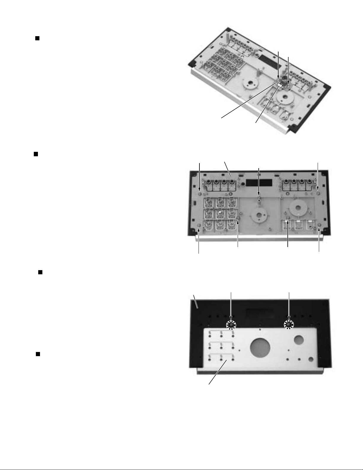
Disassembly method
RM-RE9000
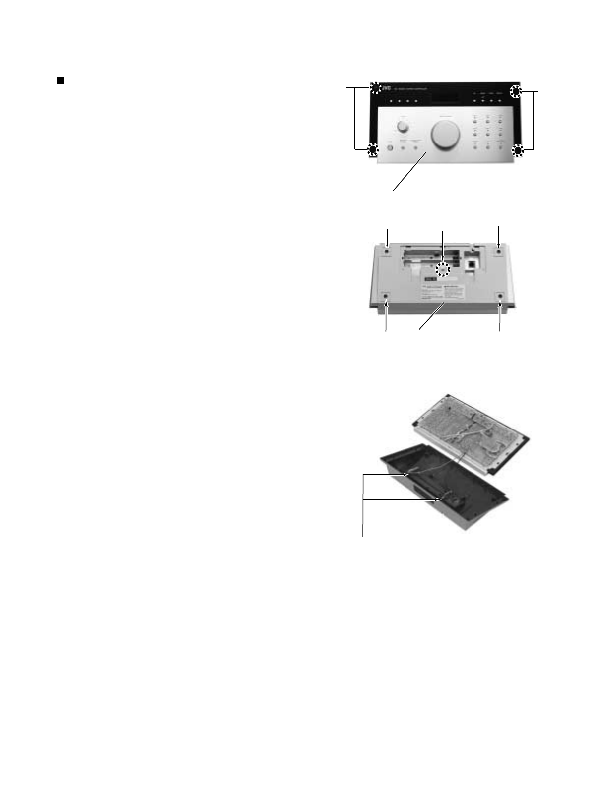
Removing the rear cover (See Fig.1 to 3)
1.
Remove the four screws A on the front with a
hexagon wrench.
2.
Place the reverse side of the set upward.
3.
After taking off the cushions from the four places,
remove the four screws B at the inside of the rear
cover.
4.
Remove the screw B' at the inside of the battery
cover.
5.
Remove the rear cover and the front panel
assembly. (Because they should have been tightly
engaged, remove them with due care.)
6.
Remove the battery holder board assembly from the
rear cover by pulling it up.
A
Front panel assembly
B
Rear cover
B
Fig.1
B'
Fig.2
A
B
B
Battery holder board
assembly
Fig.3
1-3
Page 4
RM-RE9000
Removing the remote controller
transmission board assembly (See Fig.4)
1.
Remove the rear cover.
2.
Remove the two screws C attaching the remote
controller transmission board assembly.
3.
Remove the connector CN201 connecting the main
board assembly to the remote controller transmission
board assembly.
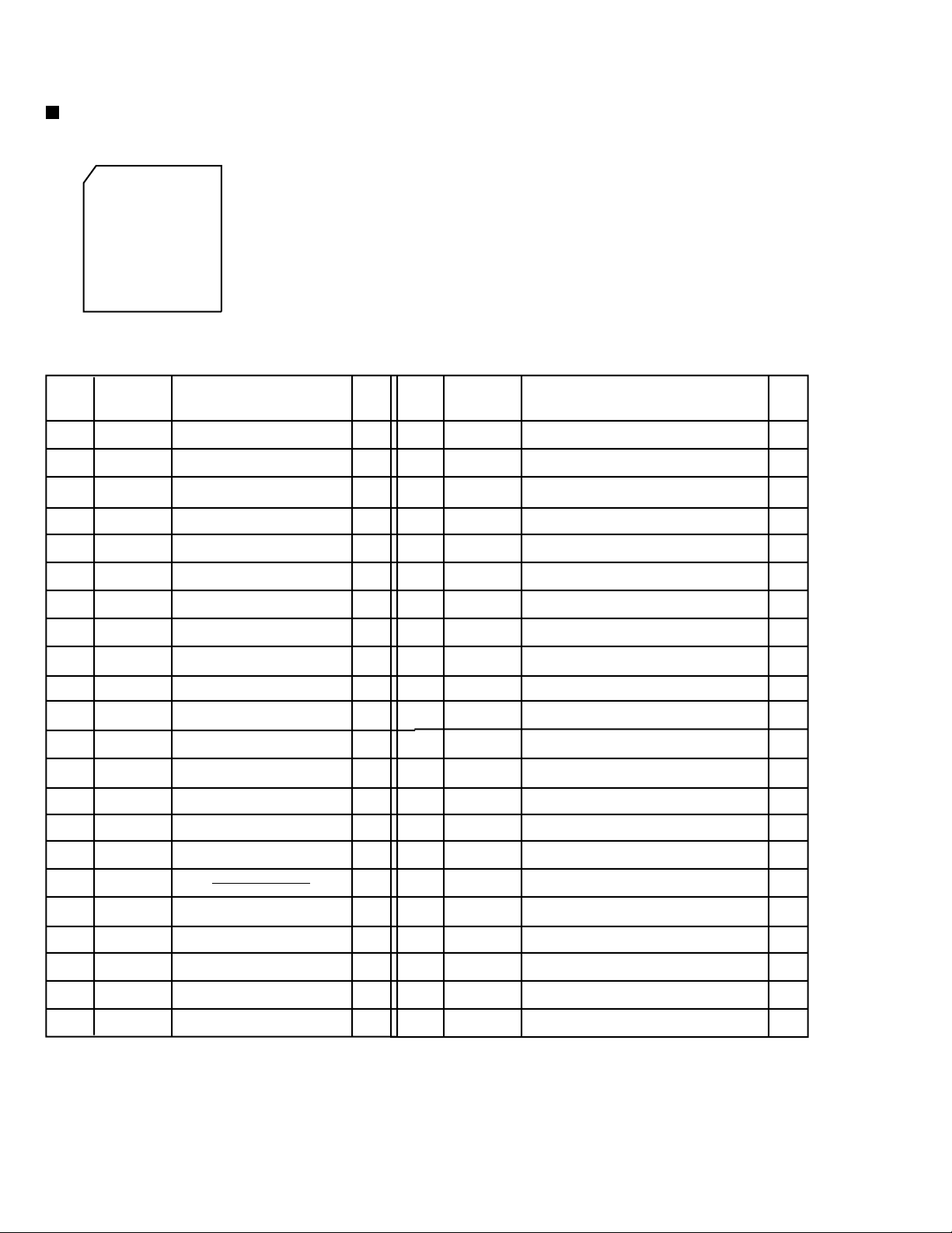
Removing the main board assembly
(See Fig.5 to 7)
Remove the rear cover.
1.
Remove the remote controller transmission board
2.
assembly.
Main board assembly
C
Fig.4
C
Remote controller
transmission board
assembly
CN201
After taking off the screws D & E attaching the
3.
volume knob and the rotary switch, remove their
knobs.
After taking off the nut F attaching the volume board
4.
assembly with a box-type driver, remove the volume
board assembly.
After taking off the nut G attaching the rotary switch
5.
board assembly with a box-type driver, remove the
rotary switch board assembly.
Remove the fourteen screws H attaching the main
6.
board assembly.
Remove the connector CN103 connecting the main
7.
board assembly to the volume board assembly, and
the connector CN301 connecting the main board
assembly to the rotary switch board assembly,
respectively.
Rotary
switch knob
H
G
E
D
Fig.5
Rotary switch knob
F
Fig.6
Rotary switch board assembly
Volume knob
Volume knob
1-4
Main board assembly
Fig.7
CN103
Volume board assembly
CN301
H
Page 5
Removing the modular jack board
assembly (See Fig.8)
1.
Remove the rear cover.
2.
Remove the remote controller transmission board
assembly.
3.
Remove the main board assembly.
4.
Remove the two screws I attaching the modular jack
board assembly.
5.
Remove the connector CN501 connecting the main
board assembly to the connector terminal board
assembly.
Modular jack board
assembly
CN501
RM-RE9000
I
I
Fig.8
Removing the switch board (See Fig.9)
1.
Remove the rear cover.
2.
Remove the remote controller transmission board
assembly.
3.
Remove the main board assembly.
4.
Remove the modular jack board assembly.
5.
Remove the seven screws J attaching the switch
board.
6.
Remove the board by lifting it.
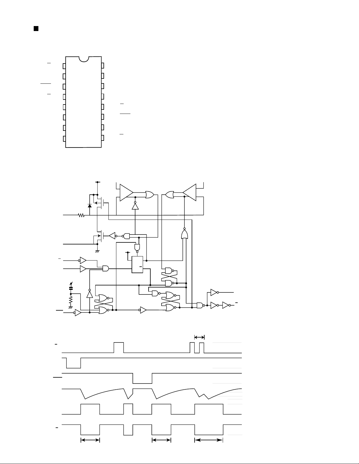
Removing the top panel (See Fig.10)
1.
Remove the rear cover.
2.
Remove the remote controller transmission board
assembly.
3.
Remove the main board assembly.
4.
Remove the modular jack board assembly.
5.
Remove the board.
6.
Remove the two screws K attaching the lens and the
top panel.
J
Lens
Switch board
J
K
J
J
J
Fig.9
J
J
K
Reminder when the top panel is
reassembled
1.
When the top panel is reassembled, use the screws
with the specified size (M3x8mm) without fail
(Screws marked K).
Using longer screws may damage the top panel and
cause the top panel unstable.
Top panel
Fig.10
1-5
Page 6
RM-RE9000
Description of major ICs
MN101CP117(IC101) : System controller
1.Pin layout
~
3444
1
33
~
11
12
2.Pin function
Pin
Symbol Symbol
No.
1
2
3
4
5
6
7
8
9
10
11
12
13
14
15
16
17
18
19
20
21
22
KY13
ROT1
ROT2
ROT3
ROT4
ROT5
ROT6
N.C
N.C
VOL1
VOL2
AD
VDD
OSC2
OSC1
VSS
NC
SDATO
BRI
SCLK
KY1
RMOUT
~
~
23
22
Key input 8
Rotary output 1
Rotary output 2
Rotary output 3
Rotary input 1
Rotary input 2
Rotary input 3
GND
GND
Volume input 1
Volume input 2
AD input
2.0V~5.0V Supply
clock output
clock input
0.0V
Serial output data
Blight adjustment
Serial clock
Key input 1
Remocon output
I/O I/O
Pin
No.
I
O
O
O
I
I
I
I
I
I
I
I
O
I
O
O
O
O
O
23
24
25
26
27
28
29
30
31
32
33
34
35
36
37
38
39
40
41
42
43
44
CK1
LATCH1
RST1
SIN1
WAKE
KY2
KY3
KY4
KY5
KY6
CK2
LATCH2
RST2
SIN2
KY7
KY8
RST
MMOD
KY9
KY10
KY11
KY12
7segment circuit clock 1
7segment circuit latch output 1
7segment circuit latch reset 1
Output data 1
Wake
Key input 2
Key input 3
Key input
Key output 1
Key output 2
LED circuit clock 2
LED circuit latch output 2
LED circuit reset 2
LED circuit data output 2
Key output 3
Key output 4
Reset
GND
Key output 5
Key input 5
Key input 6
Key input 7
FunctionFunction
O
O
O
O
O
O
O
O
O
O
O
O
O
I
I
I
I
I
I
I
I
I
1-6
Page 7
TC74VHC123AF-X(IC112) :Shift register for relay control
1. Pin layout
16
15
14
13
12
11
10
9
Vcc
1Rx/Cx
1Cx
1Q
2Q
2CLR
2B
2A
1A
1B
1CLR
1Q
2Q
1Cx
2Rx/Cx
GND
1
2
3
4
5
6
7
8
(TOP VIEW)
RM-RE9000
2. Block diagram
X/CX
R
C
X
A
B
CLR
3. Timing diagram
A
B
CLR
RX/CX
Q
V
CC
Vref Vref
L
-
Q
Q
N
+
P
V
CC
R
D
Q
F/F
CK
Q
C2
H
+
-
Q
Q
t
rr
V
IH
VIL
VIH
VIL
VIH
VIL
VCC
V
refH
V
refL
GND
VOH
VOL
Q
t
w OUT
t
w OUT
t
w OUT+
t
rr
VOL
1-7
VOH
Page 8
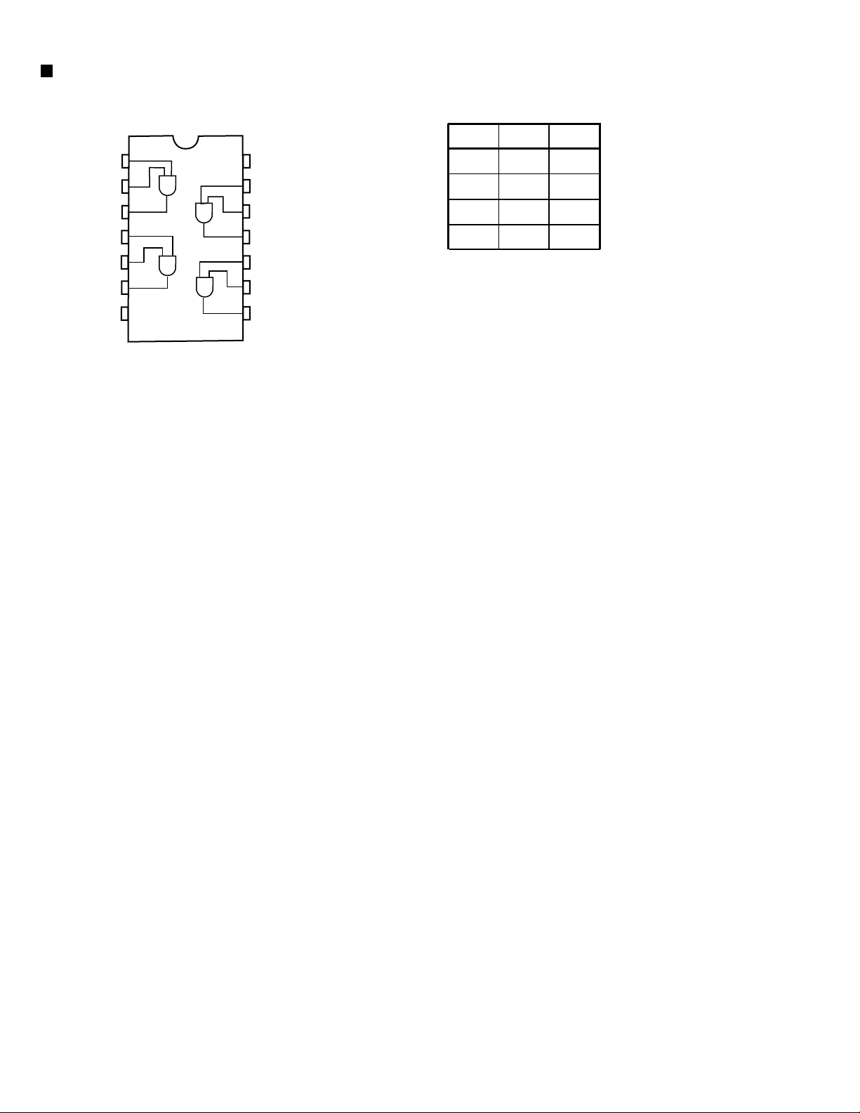
RM-RE9000
TC74VHC08F-X (IC112) :Data line buffer
1. Pin. layout 2. True table
1A
1B
1Y
2A
2B
2Y
GND
A
14
13
12
11
10
9
8
Vcc
4B
4A
4Y
3B
3A
3Y
L
L
H
H
1
2
3
4
5
6
7
(TOP VIEW)
B
L
H
L
HH
X : Don't Care
Y
L
L
L
1-8
Page 9

< MEMO >
RM-RE9000
1-9
Page 10
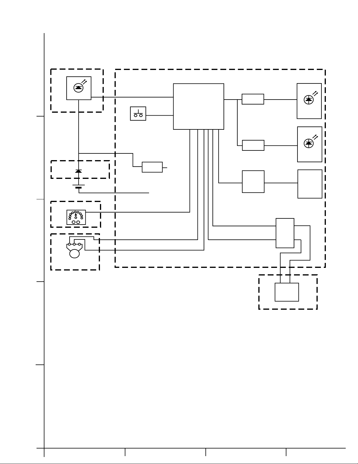
Block diagram
Transmission part
5
4
Battery
holder
RMOUT
Key1~6
Key7~13
DC-DC converter
IC103
Power
supply
GND
IC101
Micro controller
LATCH1
SIN1
RST1
CK1
LATCH2
SIN2
RST2
CK2
LED driver
IC104
LED driver
IC105
LED driver
IC106
to
IC110
PRESENCE2
PRESENCE1
SPEAKER2
SPEAKER1
MUTING
LINE1~6
ATT
EXT
RM-RE9000
LED
LED
LED
Rotary switch
ROT1 to ROT6
Data line buffer
SDA TO
IC112
3
3
1
2
VOL 2
SCL IC
Volume
Modular
jack
2
1
A
BC D
2-1
Page 11

RM-RE9000
< MEMO >
2-2
Page 12
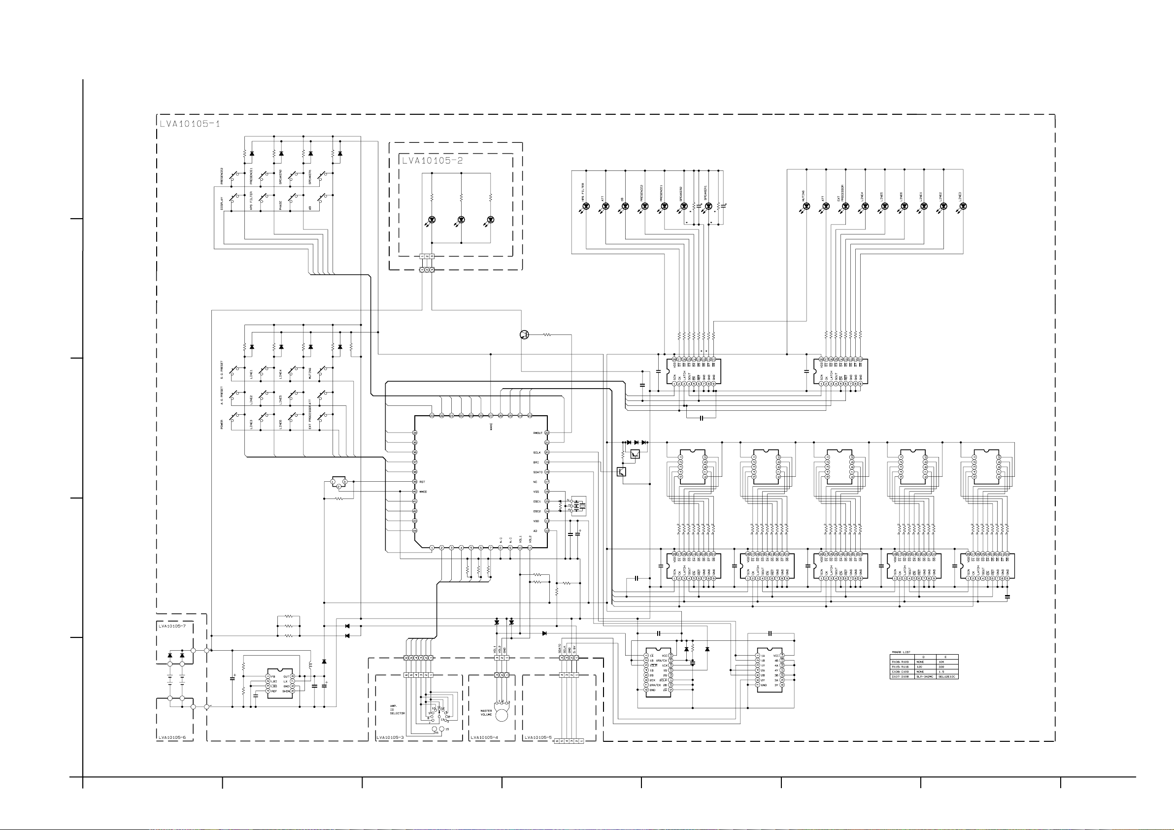
Standard schematic diagram
RM-RE9000
22K
QSW0802-001Z
S101
QSW0802-001Z
S105
R166
5
D133
1SS133-T1
QSW0802-001Z
S102
QSW0802-001Z
S106
22K
22K
R167
D134
1SS133-T1
QSW0802-001Z
S103
QSW0802-001Z
S107
22K
R168
R169
D135
KY6
1SS133-T1
QSW0802-001Z
S104
QSW0802-001Z
S108
KY4
KY5
D136
1SS133-T1
SLR-342VC-T
SLR-342MC-T
SLR-342DC-T
SLR-342DC-T
SLR-342DC-T
SLR-342DC-T
SLR-342DC-T
SLR-342DC-T
SLR-342MC-T
SLR-342MC-T
SLR-342VC-T
SLR-342MC-T
SLR-342MC-T
SLR-342MC-T
3.9
3.9
SRZ-932C-22-T14
3.9
R203
SRZ-932C-22-T14
D203
D101
D102
D103
D104
D105
R201
D201
CN201
QGA2001F1-03
KY3
KY2
KY1
CN101
QJB002-031803
SRZ-932C-22-T14
R202
D202
SLR-342MC-T
C108
R108
D107
C109
R109
D108
D109
D110
D112
D113
D114
D111
D115
SLR-342DC-T
D116
D117
4
220
270
270
270
270
270
270
120
120
330
120
120
120
120
R101
22K
22K
R170
1SS133-T1
D137
QSW0802-001Z
S109
QSW0802-001Z
S113
QSW0802-001Z
3
S117
QSW0802-001Z
S110
QSW0802-001Z
S114
QSW0802-001Z
S118
KY13
22K
R171
R172
1SS133-T1
QSW0802-001Z
QSW0802-001Z
QSW0802-001Z
1SS133-T1
D139
QSW0802-001Z
S112
QSW0802-001Z
S116
QSW0802-001Z
S120
KY11
D138
S111
S115
S119
KY12
22K
R173
KY10
D140
KY9
IC102
IC-PST529
R175
1K
NI
1SS133-T1
R174
KY8
CK2
LATCH2
KY7
RST2
SIN2
KY7
KY8
KY9
KY10
KY11
KY12
KY13
KY3
KY4
KY5
KY6
IC101
MN101CP117
ROT2
ROT1
ROT4
ROT3
SIN1
RST1
KY2
ROT6
ROT5
2
22K
22K
22K
R181
R179
R180
D153
R192
NI
R191
NI
R190
C102
0.1
IC103
MAX1674EUA-X
NI
L101
22
C103
0.1
D701
RB160L-40-X
D702
RB160L-40-X
WR701
WR101
W701 W702
QUY260-050H QUY260-050H
W601
VYH7199-001
1
W602
VYH7199-001
WR601
WR102
C101
47/6.3
NI
R177
0
R176
C104
47/6.3
D151
11E2-T5
D143
D144
11E2-T5
11E2-T5
CN102
ROT1
ROT2
ROT3
ROT4
ROT5
ROT6
QJB002-060801
CN301
QGA2001F1-06
S301
S301
S301
QSW0864-001
D152
MTZJ6.8A-T2
CN401
QJB002-030803
MTZJ6.8A-T2
JS401
QSW0867-001
CN103
QGA2001F1-03
Q101
2SD1328/ST/-X
LATCH1
CK1
KY1
R182
R183
220
R106
1M
22K
22K
D145
1SS133-T1
CN501
QGA2001C1-04
C106
0.1
R184
6.8K
QAX0246-001Z
R185
22K
X101
220/10
C107
CN104
QJB002-040904
QNZ0004-001
J501
R186
10K
SIN1
RST1
LATCH1
CK1
C123
330P
SIN2
RST2
LATCH2
CK2
1SS133-T1
1SS133-T1
D149
D148
Q103
DTB113ZK-X
Q104
DTC114YKA-X
C124
330P
1.5
1SS133-T1
D150
C112
1.5
C118
IC111
TC74VHC123AF-X
R110
330
R126
IC106
1.5
R111
R112
D120
330
330
R127
R128
D146
1SS133-T1
R113
R114
LA-401VD
330
330
R129
R130
BU2114F-X
R189
10K
C119
1.5
560
R115
R116
R117
C122
330P
LA-401VD
D121
330
330
330
R131
R132
R133
D147
1SS133-T1
330
R134
C113
1.5
IC107
330
330
R135
R136
C120
IC112
TC74VHC08F-X
330
330
R137
R138
BU2114F-X
1.5
330
330
330
R139
R140
R141
R118
C111C110
1.5
330
R142
C114
1.5
IC108
270
R119
R120
R121
R122
R124
R123
R125
IC105IC104
BU2114F-XBU2114F-X
LA-401VD
D123
330
330
330
330
330
330
330
R143
R144
R145
R146
R147
R148
R149
C115
1.5
BU2114F-X
D124
LA-401VD
330
330
330
330
330
330
330
330
R150
R151
R152
R153
R154
R155
R156
R157
C116
1.5
IC109
BU2114F-X
D125
LA-401VD
330
330
330
330
330
330
330
330
R158
R159
R160
R161
R162
R163
R164
R165
C121
330P
IC110
BU2114F-X
AB CD E F G
2-3
Page 13

Printed circuit boards
RM-RX9000
Main board (Front side)
IC109
R156
D151
R101
Q101
R161
C107
C103
R159
R176
C104
R162
C121
C116
C102
R164
R177
R165
C101
R106
IC101
IC110
R186
D148
D150
R188
R144
D153
R142
C122
C112
R147
CN101
R149
R128
D145
R152
R126
R187
R150
R131
D152
IC105
C110
R155
R133
R112
D103
CN103
C111
C113 C114
IC106
R157
R158
R160
R163
R127
R129
R134
R136
R139
R141
D120 D121 D123
IC104
R130
IC107
R132
R137
R135
R138
R140
IC108
R145
R143
R146
R148
C115
R151
R153
R154
D124 D125
R117R118R119
D109D110D111
R120R121R122
R123
D112D113D114
D115D116D117
R174
S112
S111
S110
D136
R169
S120
S116
5
R171R172R173
D138D139D140
S115
S114
R124
S119
S118
R125
4
D133
D134
D135
D147
D146
C118
R166
C119
R189
IC111
S105 S106 S107 S108
R110 R111
D101 D102
R168
R167
IC103
WR101
D144
Q104
Q103
D149
R190
R191
WR102
R192
S109
D143
R175
L101
R184
C106
IC102
X101
R182
R185
R183
R181
R180
C120
R179
IC112
S101
R113 R114 R115 R116
D104 D105 D107 D108
S113
S102
C108
R108
S103 S104
C109
R109
D137
R170
WR103
S117
CN102
CN104
Remote controller transmission board
CN201
D202
Battery holder board
WR601
W602
W701
W601
W702
WR701
Rotary switch board
CN301
S301
3
Main board (Reverse side)
D101 D102
D103
S107 S108
2
S118
1
S119
S120
D138 D139 D140
D146
D147
D136
D133
D134
D135
D115D116D117
S114
S115
S116
S110
D112D113D114
S111
D152
D153
D109D110D111
S112
CN101
D120 D121
D145
CN103
D123
D124 D125
D151
C104
C107
C101
D150
D148
D149
D104 D105 D107 D108
S101
S102
S103 S104S105 S106
WR103
Volume board
CN401
JS401
CN104
Modular jack board
X101
CN102
WR101
D144
WR102
IC102
D143
D137
S109
S113
S117
J501
CN501
2-4
HAB C DE FG
Page 14

PARTS LIST
[ RM-RE9000 ]
* All printed circuit boards and its assemblies are not available as service parts.
RM-RE9000
Area suffix
E ----------- Continental Europe
- Contents -
Exploded view of general assembly and parts list
Electrical parts list
Packing materials and accessories parts list
3-2
3-4
3-6
3-1
Page 15

RM-RE9000
Exploded view of general assembly and parts list
Block No.
17
Lower
side
16
19
Battery
1
8
board
14
Battery
board
M
1
12
13
M
M
8
2
14
8
14
15
15
3
8
5
5
15
11
6
7
4
7
Modular jack
board
7
18
9
9
7
Main
board
3-2
Rotary switch
board
Remote
controller
9
transmission
board
10
9
9
Volume board
Page 16

RM-RE9000
M1MM
(General assembly)
Parts list
Item Parts number Parts name Area
A
1 LV20618-003A TOP PANEL 1
2 LV20624-005A LENS 1
3 QYSPSP3008M SCREW 2 TOP-LENS
4 LV10323-002A BASE 1
5 LV41482-001A INDICATOR 3
6 LV41547-001A CAP 1
7 QYSPSP3010Z SCREW 6 TOP-BASE
8 LV40744-002A SOCKET BOLT 4 LENS-BASE
9 QYSDSF2608Z SCREW 16 C.B-BASE
10 QYSDSF2608Z SCREW 2
11 LV20623-001A BATT. COVER 1
12 LV41481-001A REMOTE LENS 1
13 LV10322-002A BOTTOM CASE 1
14 QYSBSF3010Z SCREW 5 BOTTOM-BASE
15 E75896-001 FELT SPACER 4 BOTTOM CASE
16 LV31626-001A VOL KNOB 1
17 LV31627-001A SEL KNOB 1
18 QYSPSPL3012Z SCREW 1 TOP-BASE
19 LV41797-001A SPACER 1 VOL KNOB
Q'ty Description
Block No.
3-3
Page 17

RM-RE9000
Q
Q
Q
Electrical parts list
Item
A
C 101 QER60JM-476Z E CAPACITOR 47MF 20% 6.3V
C 102 NCF21EZ-104X C CAPACITOR
C 103 NCF21EZ-104X C CAPACITOR
C 104 QER60JM-476Z E CAPACITOR 47MF 20% 6.3V
C 106 NCF21EZ-104X C CAPACITOR
C 107 QER61AM-227Z E CAPACITOR 220MF 20% 10V
C 108 NCF21CZ-155X C CAPACITOR
C 109 NCF21CZ-155X C CAPACITOR
C 110 NCF21CZ-155X C CAPACITOR
C 111 NCF21CZ-155X C CAPACITOR
C 112 NCF21CZ-155X C CAPACITOR
C 113 NCF21CZ-155X C CAPACITOR
C 114 NCF21CZ-155X C CAPACITOR
C 115 NCF21CZ-155X C CAPACITOR
C 116 NCF21CZ-155X C CAPACITOR
C 118 NCF21CZ-155X C CAPACITOR
C 119 NCF21CZ-155X C CAPACITOR
C 120 NCF21CZ-155X C CAPACITOR
C 121 NCS21HJ-331X C CAPACITOR
C 122 NCS21HJ-331X C CAPACITOR
C 123 NCS21HJ-331X C CAPACITOR
C 124 NCS21HJ-331X C CAPACITOR
CN101 QJB002-031803 E-S-ID WIRE C-B
CN102 QJB002-060801 E-S-ID WIRE C-B
CN103 QGA2001F1-03 CONNECTOR
CN104 QJB002-040904 E-S-ID WIRE C-B
CN201 QGA2001F1-03 CONNECTOR
CN301 QGA2001F1-06 6P PLUG ASSY
CN401 QJB002-030803 E-S-ID WIRE C-B
CN501 QGA2001C1-04 4P PLUG ASSY
D 101 SLR-342MC-T L ED
D 102 SLR-342MC-T L ED
D 103 SLR-342VC-T LED
D 104 SLR-342MC-T L ED
D 105 SLR-342MC-T L ED
D 107 SELU2E10C LED
D 108 SELU2E10C LED
D 109 SLR-342VC-T LED
D 110 SLR-342MC-T L ED
D 111 SLR-342DC-T LED
D 112 SLR-342DC-T LED
D 113 SLR-342DC-T LED
D 114 SLR-342DC-T LED
D 115 SLR-342DC-T LED
D 116 SLR-342DC-T LED
D 117 SLR-342DC-T LED
D 120 LA-401VD 7 SEGMENT LED
D 121 LA-401VD 7 SEGMENT LED
D 123 LA-401VD 7 SEGMENT LED
D 124 LA-401VD 7 SEGMENT LED
D 125 LA-401VD 7 SEGMENT LED
D 133 1SS133-T1 SI DIODE
D 134 1SS133-T1 SI DIODE
D 135 1SS133-T1 SI DIODE
D 136 1SS133-T1 SI DIODE
D 137 1SS133-T1 SI DIODE
D 138 1SS133-T1 SI DIODE
D 139 1SS133-T1 SI DIODE
D 140 1SS133-T1 SI DIODE
D 143 11E2-T5 DIODE
D 145 1SS133-T1 SI DIODE
D 146 1SS133-T1 SI DIODE
D 147 1SS133-T1 SI DIODE
Parts number Parts name Area
(Main board)
Block No. 01
Remarks
Item
A
D 148 1SS133-T1 SI DIODE
D 149 1SS133-T1 SI DIODE
D 150 1SS133-T1 SI DIODE
D 151 11E2-T5 DIODE
D 152 MTZJ6.8A-T2 ZENER DIODE
D 153 MTZJ6.8A-T2 ZENER DIODE
D 201 SRZ-932C-22-T14 LED
D 202 SRZ-932C-22-T14 LED
D 203 SRZ-932C-22-T14 LED
D 701 RB160L-40-X SB DIODE
D 702 RB160L-40-X SB DIODE
IC101 MN101CP117 IC(MCU)
IC102 PST529G IC
IC103 MAX1674EUA-X IC
IC104 BU2114F-X IC
IC105 BU2114F-X IC
IC106 BU2114F-X IC
IC107 BU2114F-X IC
IC108 BU2114F-X IC
IC109 BU2114F-X IC
IC110 BU2114F-X IC
IC111 TC74VHC123AF-X IC
IC112 TC74VHC08F-X IC
J 501 QNZ0004-001 MODULAR JACK
JS401 QSW0867-001 ROTARY ENCODER
L 101 NQL32CM-220X INDUCTOR
R 101 NRSA02J-221X MG RESISTOR
R 106 NRSA02J-105X MG RESISTOR
R 108 NRSA02J-103X MG RESISTOR
R 109 NRSA02J-103X MG RESISTOR
R 110 NRSA02J-121X MG RESISTOR
R 111 NRSA02J-121X MG RESISTOR
R 112 NRSA02J-331X MG RESISTOR
R 113 NRSA02J-121X MG RESISTOR
R 114 NRSA02J-121X MG RESISTOR
R 115 NRSA02J-331X MG RESISTOR
R 116 NRSA02J-331X MG RESISTOR
R 117 NRSA02J-561X MG RESISTOR
R 118 NRSA02J-221X MG RESISTOR
R 119 NRSA02J-271X MG RESISTOR
R 120 NRSA02J-271X MG RESISTOR
R 121 NRSA02J-271X MG RESISTOR
R 122 NRSA02J-271X MG RESISTOR
R 123 NRSA02J-271X MG RESISTOR
R 124 NRSA02J-271X MG RESISTOR
R 125 NRSA02J-271X MG RESISTOR
R 126 NRSA02J-331X MG RESISTOR
R 127 NRSA02J-331X MG RESISTOR
R 128 NRSA02J-331X MG RESISTOR
R 129 NRSA02J-331X MG RESISTOR
R 130 NRSA02J-331X MG RESISTOR
R 131 NRSA02J-331X MG RESISTOR
R 132 NRSA02J-331X MG RESISTOR
R 133 NRSA02J-331X MG RESISTOR
R 134 NRSA02J-331X MG RESISTOR
R 135 NRSA02J-331X MG RESISTOR
R 136 NRSA02J-331X MG RESISTOR
R 137 NRSA02J-331X MG RESISTOR
R 138 NRSA02J-331X MG RESISTOR
R 139 NRSA02J-331X MG RESISTOR
Parts number Parts name Area
101 2SD1328/ST/-X TRANSISTOR
103 DTB113ZK-X D TRANSISTOR
104 DTC114YKA-X D TRANSISTOR
Remarks
3-4
Page 18

RM-RE9000
Electrical parts list
Item
A
R 140 NRSA02J-331X MG RESISTOR
R 141 NRSA02J-331X MG RESISTOR
R 142 NRSA02J-331X MG RESISTOR
R 143 NRSA02J-331X MG RESISTOR
R 144 NRSA02J-331X MG RESISTOR
R 145 NRSA02J-331X MG RESISTOR
R 146 NRSA02J-331X MG RESISTOR
R 147 NRSA02J-331X MG RESISTOR
R 148 NRSA02J-331X MG RESISTOR
R 149 NRSA02J-331X MG RESISTOR
R 150 NRSA02J-331X MG RESISTOR
R 151 NRSA02J-331X MG RESISTOR
R 152 NRSA02J-331X MG RESISTOR
R 153 NRSA02J-331X MG RESISTOR
R 154 NRSA02J-331X MG RESISTOR
R 155 NRSA02J-331X MG RESISTOR
R 156 NRSA02J-331X MG RESISTOR
R 157 NRSA02J-331X MG RESISTOR
R 158 NRSA02J-331X MG RESISTOR
R 159 NRSA02J-331X MG RESISTOR
R 160 NRSA02J-331X MG RESISTOR
R 161 NRSA02J-331X MG RESISTOR
R 162 NRSA02J-331X MG RESISTOR
R 163 NRSA02J-331X MG RESISTOR
R 164 NRSA02J-331X MG RESISTOR
R 165 NRSA02J-331X MG RESISTOR
R 166 NRSA02J-223X MG RESISTOR
R 167 NRSA02J-223X MG RESISTOR
R 168 NRSA02J-223X MG RESISTOR
R 169 NRSA02J-223X MG RESISTOR
R 170 NRSA02J-223X MG RESISTOR
R 171 NRSA02J-223X MG RESISTOR
R 172 NRSA02J-223X MG RESISTOR
R 173 NRSA02J-223X MG RESISTOR
R 175 NRSA02J-102X MG RESISTOR
R 176 NRSA02J-0R0X MG RESISTOR
R 179 NRSA02J-223X MG RESISTOR
R 180 NRSA02J-223X MG RESISTOR
R 181 NRSA02J-223X MG RESISTOR
R 182 NRSA02J-223X MG RESISTOR
R 183 NRSA02J-223X MG RESISTOR
R 184 NRSA02J-682X MG RESISTOR
R 185 NRSA02J-223X MG RESISTOR
R 186 NRSA02J-103X MG RESISTOR
R 189 NRSA02J-103X MG RESISTOR
R 201 NRSA02J-3R9X MG RESISTOR
R 202 NRSA02J-3R9X MG RESISTOR
R 203 NRSA02J-3R9X MG RESISTOR
S 101 QSW0802-001Z TACT SWITCH
S 102 QSW0802-001Z TACT SWITCH
S 103 QSW0802-001Z TACT SWITCH
S 104 QSW0802-001Z TACT SWITCH
S 105 QSW0802-001Z TACT SWITCH
S 106 QSW0802-001Z TACT SWITCH
S 107 QSW0802-001Z TACT SWITCH
S 108 QSW0802-001Z TACT SWITCH
S 109 QSW0802-001Z TACT SWITCH
S 110 QSW0802-001Z TACT SWITCH
S 111 QSW0802-001Z TACT SWITCH
S 112 QSW0802-001Z TACT SWITCH
S 113 QSW0802-001Z TACT SWITCH
S 114 QSW0802-001Z TACT SWITCH
S 115 QSW0802-001Z TACT SWITCH
Parts number Parts name Area
(Main board)
Block No. 01
Remarks
Item
A
S 116 QSW0802-001Z TACT SWITCH
S 117 QSW0802-001Z TACT SWITCH
S 118 QSW0802-001Z TACT SWITCH
S 119 QSW0802-001Z TACT SWITCH
S 120 QSW0802-001Z TACT SWITCH
S 301 QSW0864-001 ROTARY SWITCH
W 601 VYH7199-001 BATTERY SPRING
W 602 VYH7199-001 BATTERY SPRING
X 101 QAX0246-001Z RESONATOR
Parts number Parts name Area
Remarks
3-5
Page 19

RM-RE9000
Packing materials and accessories parts list
P5
A1 A4
Block No.
Block No.
M
M
2
M
M
3
M
M
P2
P4
P3
P1
3-6
Page 20

RM-RE9000
M2MM
)
)
M3MM
(Packing)
(Accessories)
Parts list
Item Parts number Parts name Area
A
P 1 LV31629-002A CARTON BOX 1
P 2 LV31630-001A CUSHION(L
P 3 LV31631-001A CUSHION(R
P 4 QPC02204515 POLY BAG 1 FOR SET
P 5 QPB01702404P POLY BAG 1 FOR INST
Q'ty Description
1
1
Parts list
Item Parts number Parts name Area
A
A 1 LVT0653-001A INST.BOOK 1 ENG
A 2 ----------- AL BATTERY 2
A 3 QPH01501510 SHEET 1 AL BATTERY
A 4 BT-54013-2 W.CARD 1
Q'ty Description
Block No.
Block No.
3-7
Page 21

RM-RE9000
VICTOR COMPANY OF JAPAN, LIMITED
AUDIO & COMMUNICATION BUSINESS DIVISION
PERSONAL & MOBILE NETWORK BUSINESS UNIT. 10-1,1chome,Ohwatari-machi,Maebashi-city,371-8543,Japan
(No.20934)
Printed in Japan
200104(V)
Page 22

Page 23

Page 24

Page 25

Page 26

Page 27

Page 28

Page 29

Page 30

Page 31

Page 32

Page 33

Page 34

Page 35

Page 36

Page 37

 Loading...