

Page 1
RG-M10BU
JVC
RG-M10BU
Contents
Safety
Preroution.s
lnportan.t for
Laser Products
Instruction.
Book
Description
of
!Cs
lJWassr.mbly Procedures
Adj~trnen./:
Procedures
Flow
of
Functional
OperatWn
Until
TO(?
is
Read
---------
---
-----
1-2
1-3
1-4
1-12
1-36
1-38
1-40
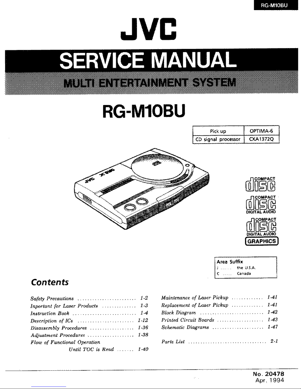
Pick
up OPTIMA-6
CD
si9r1al
processor CXA1372Q
Area Suffix
wo§@
cQJo§®
DIGITAL
AUDIO
cQJo~®
DIGITAL
AUDIO
(GRAPHICS
I
the
U.S.A.
C
Canad<1
!faintenance
of
Laser
Pickup
Replacement
of
l,ru;er Pickup
Block
Diagram
Printed Circuit Boards
Schematic
Diagrams
Parl6
List
141
1-41
142
l
4.3
1-47
2-1
No.
20478
Apr.
1994
Page 2
RG-M10BU
-Safety
Precautions---------------------~
1.
The design
of
this
product
contains special hardware and many circuits and components
specially
for
safety purposes. For continued
protection,
no changes should be made
to
the
original
design
unless
authorized
in
writing
by
the
manufacturer. Replacement
parts must
be
identical
to
those used in
the
original circuits. Services should be performed by
qualified personnel only.
2.
Alterations
of
the
design
or
circuitry
of
the
product
should
not
be made. Any design
alterations
of
the
product
should
not
be made. Any design
alterations
or additions
will
void
the
manufacturer's
warranty
and
will
further
relieve
the
manufacture
of
responsibility
for
personal
injury
or
property
damage resulting therefrom_
3.
Many
electrical
and
mechanical
parts
in
the
products have special
safety-related
characteristics.
These
characteristics are
often
not
evident
from
visual
inspection
nor
can
the
protection
afforded
by
them
necessarily
be obtained by using
replacement
components
rated
for
higher
voltage,
wattage,
etc. Replacement
parts
which
have these
special
safety
characteristics are
identified
in
the
Parts List
of
Service Manual.
Electrical components
having such features are
identified
by shading on
the
schematics and by (
i__h)
on the Parts
List in
the
Service Manual_
The
use
of
a substitute
repalcement
which does
not
have
the
same safety characteristics
as
the
recommended
replacement
parts shown in
the
Parts List
of
Service
Manual
may create shock, fire,
or
other
hazards.
4.
The leads
in
the
products are
routed
and dressed
with
ties,
clamps,
tubings, barriers and
the
like
to
be separated
from
live
parts, high
temperature
parts, moving parts and/or sharp
edges
for
the
prevention
of
electric
shock and
fire
hazard. When service
is
required,
the
original
lead
routing
and dress
should be observed, and
it
should
be confirmed
that
they
have been
returned
to
normal,
after
re-assembling_
5.
Leakage
currnet
check (Electrical shock hazard testing)
After
re-assembling
the
product,
always perform an
isolation
check on
the
exposed metal
parts
of
the
product
(antenna
terminals,
knobs,
metal
cabinet, screw heads, headphone jack,
contorl
shafts, etc.)
to
be sure
the
product
is
safe
to
operate
without
danger
of
electrical
shock.
Do
not
use
a
line isolation
transformer
during
this check.
• Plug
the
AC
line
cord
directly
into
the
AC
outlet.
Using
a "Leakage Current
Tester",
measure
the
leakage
current
from
each exposed
metal
parts
of
the
cabinet,
particularly
any exposed
metal
part
having a
return
path
to
the
chassis,
to
a
known
good
earth
ground.
Any
leakage
current
must
not
exceed 0.5mA
AC
(r.m.s.).
•
Alternate
check
method
Plug
the
AC
line
cord
directly
into
the
AC
outlet.
Use
an
AC
voltmeter
having, 1,000
ohms per
volt
or
more sensitivity in
the
following
manner.
Connect
a
1,SOOn
10 W
resistor
paralleled by a 0.15
µF
AC-type
capacitor between an exposed
metal
part
and a
known
good
earth
ground.
Measure
the
AC
voltage
across
the
resistor
with
the
AC
voltmeter.
Move
the
resistor connection
to
each exposed
metal
part,
particularly
any exposed
metal
part
having a
return
path
to
the
chassis, and
meausre
the
AC
voltage
across
the
resistor.
Now, reverse
the
plug
in
the
AC
outlet
and
repeat
each measurement_
Any
voltage
measured must
not
exceed
0.75 V
AC
(r.m.s.).
This corresponds
to
0.5
mA
AC
(r.m.s.).
~-~AC
VOLTMETER
r:::::::;z:"]
(Having 1000
[____L_J
ohms/Volts,
or more
sensitivity_)
.----
-0
0-
r--
~
~
15µF
A(
TYPE
·'
Pl<1ce
this
•
~-'--+~~+--"-•Probe
on
e«h
e.po"d
1soon
iow
metal
rxirt.
Good
earth
ground
IA!arning---------------------------
1.
This
equipment
has been designed and manufactured
to
meet
international
safety standards.
2.
It
is
the
legal responsibility
of
the
repairer
to
ensure
that
these safety standards are
maintained.
3.
Repairs
must
be made in accordance
with
the
relevant
safety standards.
4.
It
is
essential
that
safety
critical
components are
replaced
by
approved parts.
5.
If
mains
voltage
selector
is
provided, check
setting
for
local
voltage.
1-2
(No.
20478)
Page 3
RG-MlOBU
Important
for
Laser Products
1.
DANGER:
Invisible laser radiation when open and
>nterlod: failed or defeated. Avoid
direct
exposure
to
beam.
2.
CAUTION:
There
are
no
serviceable parts inside
the
Laser
Unit.
Do
not
disassemble
the
Laser
Unit
Replace
the
complete
Laser
Unit
if
it
malfunctions.
3.
CAUTION
: The compact disc player uses invisible
laser r;:idiation and
is
equipped
with
safety switches
which
prevent emission
of
rad1at1on
when
the
drawer
is
open and
the
safety interlocks have failed
or
are
defeated.
It
is
dangerous to
defeat
the
safety
switcfies
VARN
ING:
Osynl1g
laserstr;"lln1ng
nllr
denna del ar
Oppnad
och
sp~rren
llr
urkopplad.
Betrakta
ej strl'llen.
VARO
: Avattaessa
Ja
suOJalukitus oh1tettaessa
olet
altt11na
niikymattomalle lasersliteilylle.
Ala
katso sllteeseen
REPRODUCTION
AND
POSITION OF LABELS
4.
CAUTION:
If safety switches malfunction,
the
laser
1s
able
to
function
5.
CAUTION:
Use
of
controls, adjustments
or
performance of procedures
other
than
those
specified herein may result
1n
hazardous radiation
exposure.
6.
CAUTION:
The compact disc player provides a
laser diode
of
wavelength 780-790nm and optical
output
power typical 3mW
at
the
laser diode.
ADVARSEL:
Usynl1g
laseritr!ling
ved
l'lbning, nlir
sikkerhedsafbrydere er ude
af
funkt1on Undgl!i
udsaettelse
for
strAling.
ADVARSEL:
Usynlig laserstrl!iling ved l!ipning, nlir
sikkerhetsbryteren er avslott_ unngl!i utsettelse
for
str!l1ng
WARNING
LABEL
(Only for the canada)
OANGl'R'
mv,.cbl•
l.,er
iadiatlon
when
open and
interlock
fa1led
er
defeated.
AVOID OIRlCT
EXPO I URE
TO
BEAM. (e)
ADVARSEL' U>ynllng 1
..
er·
>VMln9
vod
~bnlng.
n~r
\kerheds.aibrydere
er
ude
at
lunktlon.
Undg~ud..,t·
el>e
for
>tr~l'"g
(d)
ENR-005
VARNING.
O.inling
10>0<-
>VMlng
n~'
denna del
~-Oppnad
o'h
•p.\rren
~r
urk0ppled. 6etro<to ej
•tMen (•)
VARO.
Avstta"'s.a
ja
soo-
aluk<to1
ohitetta"'sa
olet
alttHna
n~kym~ttom~lle
1.,e,~te;lylle
Ala
k•Uo
>Ate••••n
If)
0
ENR·006
(No. 20478) 1-3
Page 4
Since
tha
JVC
X'
EYE
features
CO-ROM
playing.
11
can
be
used
10
en10Y
games
on
Sega
CDs
along
with
games
on
Genesis
cartridges,
music
on
audio
cos,
and
karaoke
music
on
CD+Gs
Games
SEGA
CDs
Karaoke.
CO+Gs
MUSIC
COS
Games:
The
JVC
X'EYE
is
compatible
w1tti thBse
disc
types·
rn'lo~tQl
rnJoflltQl
DIGITAL AUDIO
rn'lo~tQl
DKllTAL
AUDIO
[GRAPHICS
I
SEGA
CD
Games
(CO-ROM)
Audio
MUSIC
(CO)
:
..............................................................
·.
•
JVC
x·
EYE
can
oe used
to play
games
on
:
SEGA
CDs
and
GENESIS
cartridges
SEGACD.
GENESIS-
. .
................................................................
JVC
X'EYE
SYSTEM
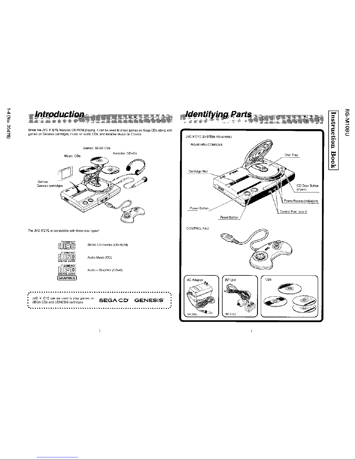
RG-M10BU
RG·MlOBU
CONSOLE
cartridge
Slot
Reset
BLJlton
/
CONTROL
PAD
CD
Door
Button
{Open)
Power/Access
lnd.cators
Control Port 1and 2
"'
Gl
;!:
~
0
"'
c
Page 5
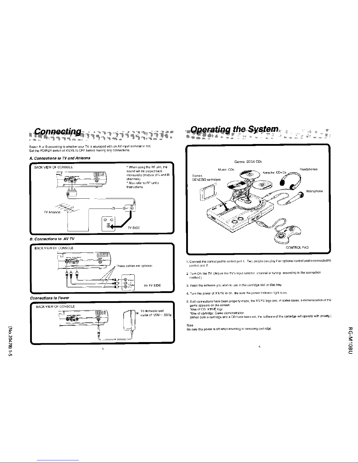
Select
A
or
B
according
to
whether
your
TV
is
equipped
with an
AV
input
terminal
or
not
Set
the
POWER
switch
of
X'EYE
to
OFF
befOr$ making
any
connections
A, Connections
to TV
and
Antenna
BACK
VIEW
OF
CONSOLE
B.
Connections
to
AV
TV
BACK
VIEW
OF
CONSOLE
Connections
to
Power
BACK
VIEW
OF
CONSOLE
•When
using
lhe
RF
unit,
the
sound
w•ll
be
played
back
monaurally
(mixture
of
Land
R
ohannels)
'Also
refer
to
RF-units
Instructions
-Lr,.r.;oF-~~
[Jll'1
'·.::!~~
~
To
domestic
wall
oullel
of
120V~·
.60Hz
Gamos
SEGA
CDs
Music
CDs
Games.
GENESIS
cartridges
Microphone
CONTROL
PAD
Connect
the
control
pad
tc
control
port
1.
Two
people
can
piny
•I
an
optional
control
pad
1s
connected
10
control
pen
2
Turn
ON
the
TV
(Ad1usl
the
TV's
input
selector. channel
or
tuning
according
lo
the
connection
method)
3_
Insert
the
soflware
you
wish
to
use
1n
the
cartridge slot
or
disc
tray_
4.
Turn
the
power
of
X'EYE
to on.
Be
sure
the
power
1nd1cator light
15
on
5
II
all
connections have
been
properly made_
the
X'EYE
logo
anc,
1n
some
cases,
a
demonstration
of
the
game
eppears
on
tho
screen
·uoo
of
CD:
X'EYE
logo
·use
af
cartridge:
Game
demonstration
{When
both•
canndge
and
a
CD
have
been
sol,
the
software
of
the
cartndge
will
operate with
prionty_)
Note
Be sure
the
powe<
1s
ott
when 1nsert1ng
or
removing
cartridge
"'
Gl
'
;::
~
0
"'
c
Page 6
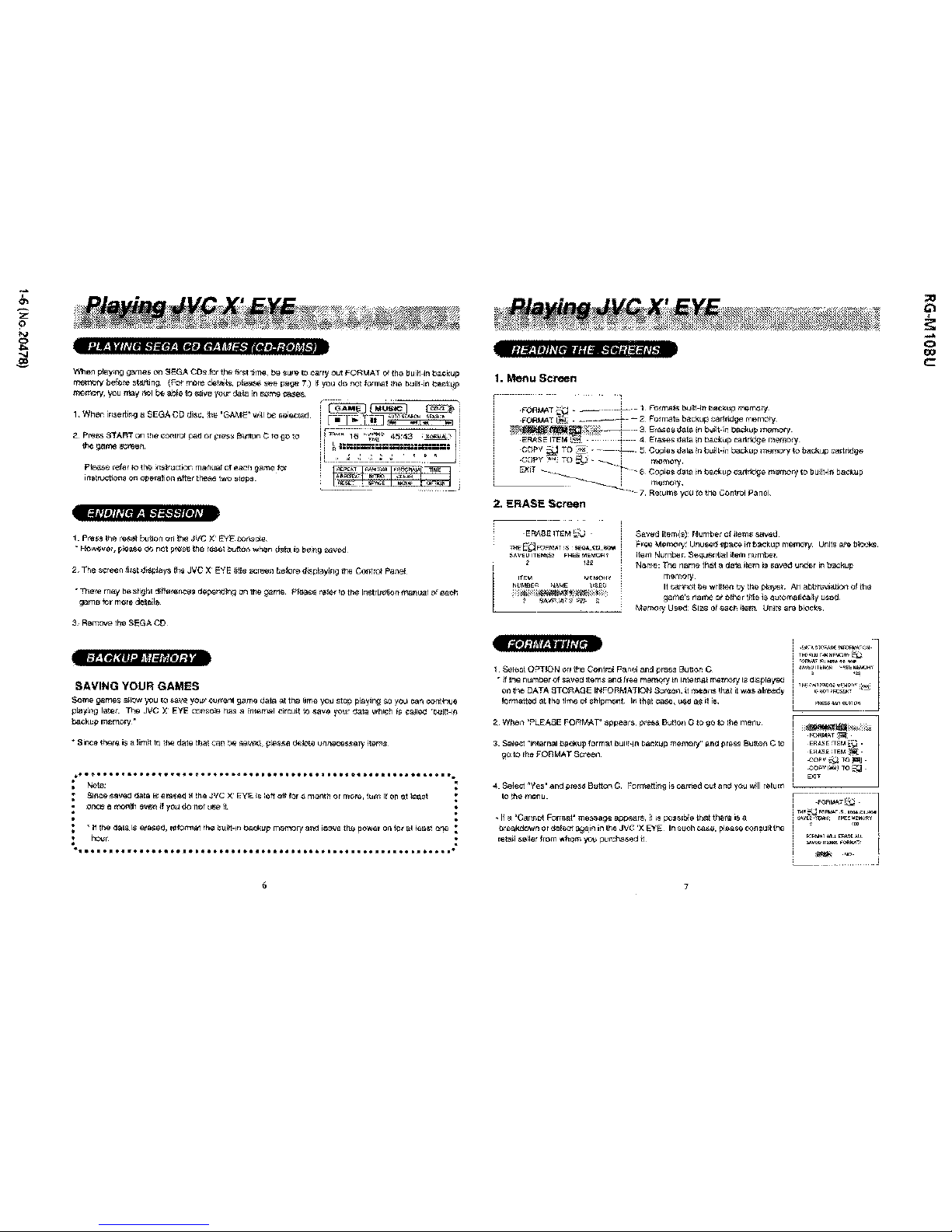
PLAYING
SEGA
CD
GAMES
(CD-ROfvlS)
1. When
insertiny
a
SEGACO
disc,
th~
'GAME"
Will
t)e
Geiected.
2-
Pre,;;
START
"'1
lh<ir
oontrOf oad or
P"'~"
i!ll<tl<>~
C
tQ
go
to
lhe
game
scroon.
Plea>~
refer
!Q
thQ
:n•lructton
manu~f
o!
emoh
gam<l
fQ<
1notruction• on
QP&ra!1on
afte•
lhe.-a
two
ste>ps.
ENDING
A
SESSION
1_
Pmos
th'>
r<l-W't
but1on
i:m
too
J\/C
X'
E'fE
00(.Sr>til-
r--r:;A
....
"'J
1
Mu~_1
~
i
1•--r~
Till
,:w···"tr1.Z'"'"
'"'
'r
--------
!
i
'"'"
16
-·~:::·
4S·43
·"°""Ii...'
: : i
:==========
i
l
__
:·~"--·:_
_
_,__,:__,!_
_____
_
ffi~,\"::'
\'::7~"'1;;]
•
Ho""'~"',
p!Qase
cl<;
Mt
pros~
too
r<IOOt
bunon
"""""
d~ta
is b6:ng
MVed
2.
T>1e
8"reen
first~t$plays
Ills
JVC
X'
EYE
trtle &eroon
~e!ored1splaylng
ltlB CootrO! Panel
•
The-re
m")'
""
sl:gh!
difklrorics•
depe'1dlnq on
ttte
g:ame.
Plt!as~
re!e< to
tt16
lnstrLl'Otion
m&nual
of
eact;
game
ror
more
delb>il$
3_
Rem(IVe
the
SEGA
CD
BACKUP
MEfli!ORY
SAVING YOUR GAMES
Same
!JI!"'~"'
ollqw
'{llU
10
save
yowr
~<Jr<<>"1
IJ'lrM
da!a
"'
the
Orne
you
stop playrng so
you
can
ooritlnu~
playing
later. Tha
JVC
x·
EYE
console has a
inlerMI
circuit
to
save
your data wh•!:h
ir;
c.\IJIOO
,oolr.-:<1
Mckup
memory
"
................................................................
'
N~:
:
S11100M'1<ld
data
fe
era~e<I
~
!h<>
JVC
x·
EYE.
ls
Iott
all
!or
a
momr
or
more,
tum
Ir
on
at
least
<JO<JS-
a month
l;1lflfl
i!
y~
d-0
net
u~e
it
•
tt
1he
dalals
e~ased,
"'!onnat
tl>e
ouin·>r>
""'°"'IP
memory
~nd
ieave
!lw
oower
on
tot
al leaM
one
""'
.
.
................................................................
READING THE
SCREENS
1.
Menu
Screen
-FORMAT~
•
-+-
--
1
Fcrma!o
t>o.J>tt-in
bac<up
mem'"'i'-
fOAMA'"
~
--'--
-
2
>'ormato baci<up
cartlldge
''"•moi--y.
·~•ii£i\~*---+·-
3
E<Mesdala
lr1
built-in
t>aci<up
,,.,.,rnory.
-ERASE
11"EM
o§
-
--
-+-----
4
Er<1SB•
da1a
In backcip
ra~ndge
merwry.
-COPY
~
TO~
• -
---+----
s
Gopie•
data
In bciilHn backup
""'rwry
lo
baci<up
Ga<1rld'J"
·COPY
'".
TO
a;
.
----
i
memory'
EX:!
------------------
-<!"
-·
6
Coples
<futa
,n
backup
cartridge
msmory
!o
bulit-ln backup
~-------.._:__,
memo>y.
·-
7.
Re:~m&
you
to
tH.:.
Control Panel.
2.
ERASE Screen
-ERASE
ITEM~{)
SRvad
Item(•)·
r~umber
o!
•temssaved
ll1EEl;'.:lFORW'11S
OE<IA._00
__
>AV<U
in;"">>
'"""
'"'MORr
Cree Merno<y:
Unuood1lJla~
inbi.cl<uP mmnory. Units
am
blo~'ks.
;\em Numl><lr. S"'fUSn!ial
~""'
numbef.
2
'20
"""
"'"'°"'
Name:
the
name
that a
d"1>1
item'"
saved
und6r
1n
b""klJI'
m.:.morv
Nl1MBE~
>U\ME
U"EU
: :
'·*-''
'iM..,,,'.l':I;~--:~,;.·
/ "-''P''A'J
>"lJ-
'
11
cannot
be wr1uen oy tho
pla)'!lt.
An
atlbro>1ab00 o!
mo
game's narrie
01
omer
Hile
is
<1U:Cmar:cai!y
UO>ld.
Memo!)'
Us&d.
Siu
m
eacr--
1!em.
Units ara
bl<Jcks.
FORfi/IA TTING
1 Se1.,ot
OPTION
""
the
Cootroi
Fanai
and
press
Sl>non
C
• lf
!he
mm1ber
o1
""''ted
'terns
ood
Jrn.e
memory
rn
1nternat
memory
12
d•spley&d
on
tf1e
DA
TA
STOF!AGE
INFORMATION
$otean.
>t
meaMS that
rt
was
alre.sdy
kJrmat10d
at
th.s
time
ol
shlpmGnt. In
H1<it
c~S<l,
l>$EI
M
rt
lo.
2.
When
'PLEASE
FORMAT'
appears, pr<*S.
But!l)ll
G
K>
90
K>
the
menu
3_
Select
"interMI
Woci<up
format
l>ullHn
b""kuD
memor(
11nO
press
Button
C to
go!()
th~
FORMAT
Screen
4_
Select
"Yes'
and
pres~
Sutton
C.
Formattim;i is
car""d
oul
amt
you will
r<>turn
to ttie menu_
, ll a "Carino\ Form&t•
massage
appears, 0
'"
po•srbfa
lC!lflt
th111r~
·~a
breakdown
or
<leloct
age1n
in
the
JVG 'X
EYE
In such
""""'·
pl.,es<)
con•l>lt!he
retari
..:.11$1
horn
..ttqm
)'Q\.I
purohss~d
tt
!
''"''-'~"'J"
i
:;::;:~~
~·.:.~:;,,.n-
:
'~'""'"~
~"""""°"'
!
'
"'
!
'"'
'~'"""""
"'·'0""
·.(-"<
I
<-.O"F<S<><'
-
':
""""''""""""
~-·:<xx·So
-FORW\f
'llif
ERASE
rrEr>
~\_1
·
<>1"8~
"""
'."'l
-
-CO•<;;>:lTIJ~-
-COOVl°"l
TO
;:Q
-
'"'
™'~"'-"·'
'""-"-""'
'-''''""'''"'"
'"'''""'--""'
"
""'"'.,"-"""""'"-'
'"'""""""'
"''"''''
Page 7
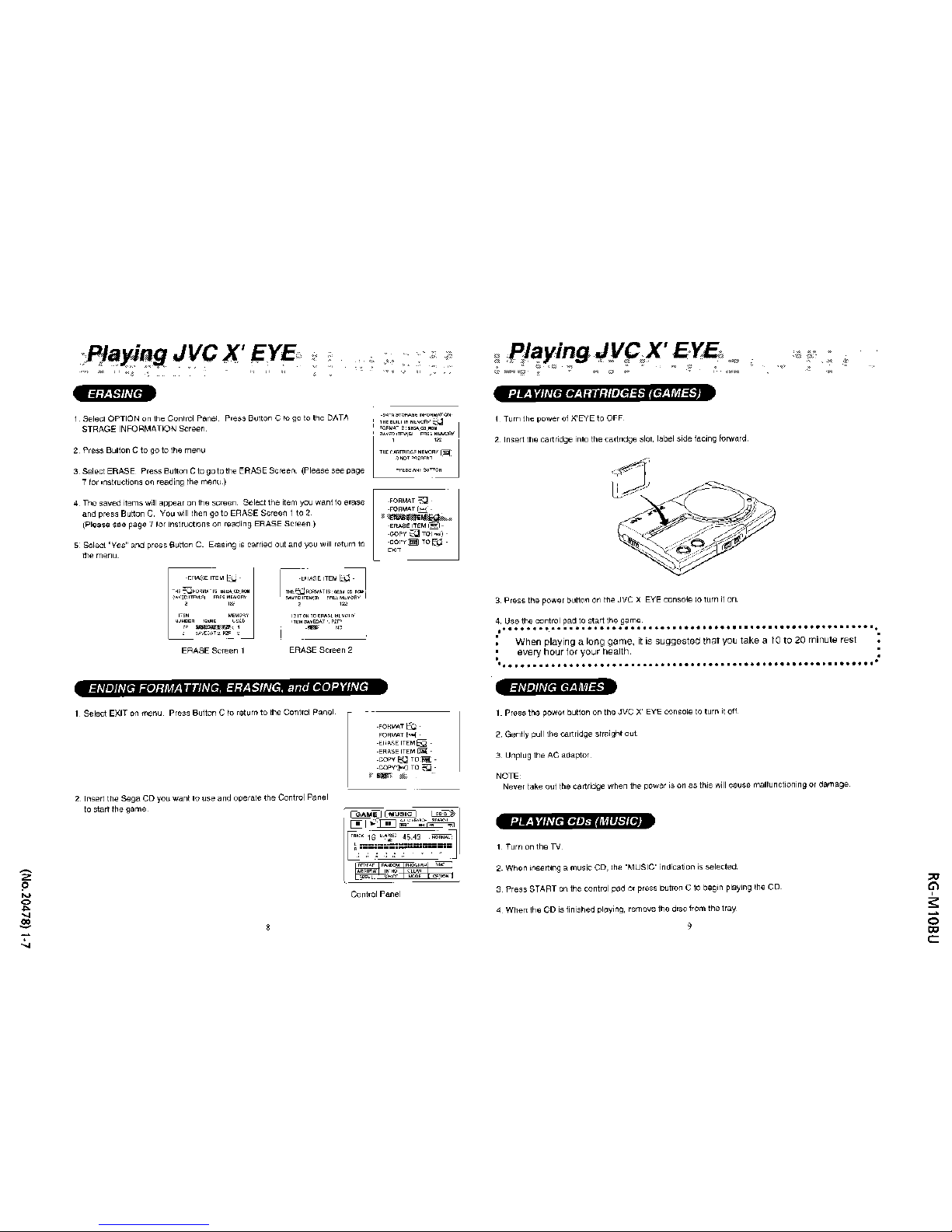
ERASING
Selecl OPTION
on the
Control Pane:
P<ess
Button
C
to
go
to
the
D/\T/\
STRAGE INFORMATION Screen
2.
Press Bulton C
to go to the
menu
3.
Select ERASE
Press Button
C
to
goto
the
ERASE Screen. (Please
see page
7
lor
onstrnct1ons
on reading the
m~nu)
4.
Tho saved items
will
appear on the
screen Select
the item
you
want
to
erase
and press Button
C.
You will
then go
to
ERASE
Screen
1 to 2
(Please
see
page 7
lor
1nstruct1ons
on reading
ERASE
Screen)
5
Select
'Yes"
and
press
Button
C_
Erasing
1s
earned
out and you
will
r~turn
to
the
menu_
-
~
-cr
..
SE
ITEM
b.,;-
-,~:;:;:;>o"~-,;
""'"""
''"'''"'"·"
"""'"""'
'
"'
,-,"
"'"o"
""'""
"""'
""
"--·
'
•,lo/[""
""
'
ERASE
Screen
1
''
"°"
'°""''
'"
"""
""
"''""''
""
-
ERASE Screen
2
ENDING FORMATTING, ERASING,
and
COPYING
1
Select EXIT
on
menu
Press
Button
C
!o
ra1um
to the
Contml Panel
_,.-,
""""'
'">""""''-0"
'""""' '""""'"
::'.J
"'"'- ,
·=-o·
~·
I
:::::::.:.:;,~;·I
'•o•
..,,,,.,
"''"' '"'
'"~c"
~--
-FORMAT
:;:a
·FORMAT
f-
-
·-ae~~
-ERASE
ITEM
1""'1-
-GOPY
SJ
TO-,;;._,
-
-COr•v
~
TO
8.:l
-
EXIT
-FOHMAT
f.'Q
-
FORMAT
I!"'"
-
-<I
•ASE
ITEM
E_Q
-
-ERA"E
ITEM
[!.i{ -
-GOPV
SJ
TO
Jl!I
-
-GOPY'}-"l
TO
::\J-
llllfr
A '
2 Insert
tha
Sega
CD
you
want
10
use
and operate
!he Control Panel
to start !ha
game
C<>AM~_J
1_.,.USIC
I
~
~I
•'J:!!J
""'"":;·~
~~:~:~~~::~~~.-;;~
Control Panel
'""""'"
~
"'~'
PLAYING CARTRIDGES (GAMES)
Turn the power
of X'EYE
to
OFF
2_
Insert
the
cartridge
1n10
the cartndge
slot,
lat>el
side facmg forward.
3
Press
the power
button
on the
JVC
X
EYE console
10
turn
1t
on.
4.
Use the
control pad
to s!art
the game
...............................................................
"
When
playing
a long
game,
it
is
suggested that
you
take a
10
to
20
minute rest
, every hour for your
health. ,
................................................................
ENDING
GAMES
1_
Press the
powe<
t>utton
on the
JVC
X'
EYE console
to turn
1t
off
2.
Gently pull
the
cartridge stmight
out
3
Unplug
the
AC aOaptor
'o~
Never take out
the cartridge
when the power
1s
on
as
this
will c:ause maltunct1onin9
or
damage
PLAYING
CDs
(MUSIC)
Turn on
the
TV
2-
Whon >nsertmg
a
music
CD, Iha "MUSIC" indication
1s
selected.
3 Press
START
on
the
control pad
01
press button
C
to
bag1n
playing lhe CD.
4
When
the CD
1s
finished playing,
remove
the d•sc
from the tray
-
0
"'
c
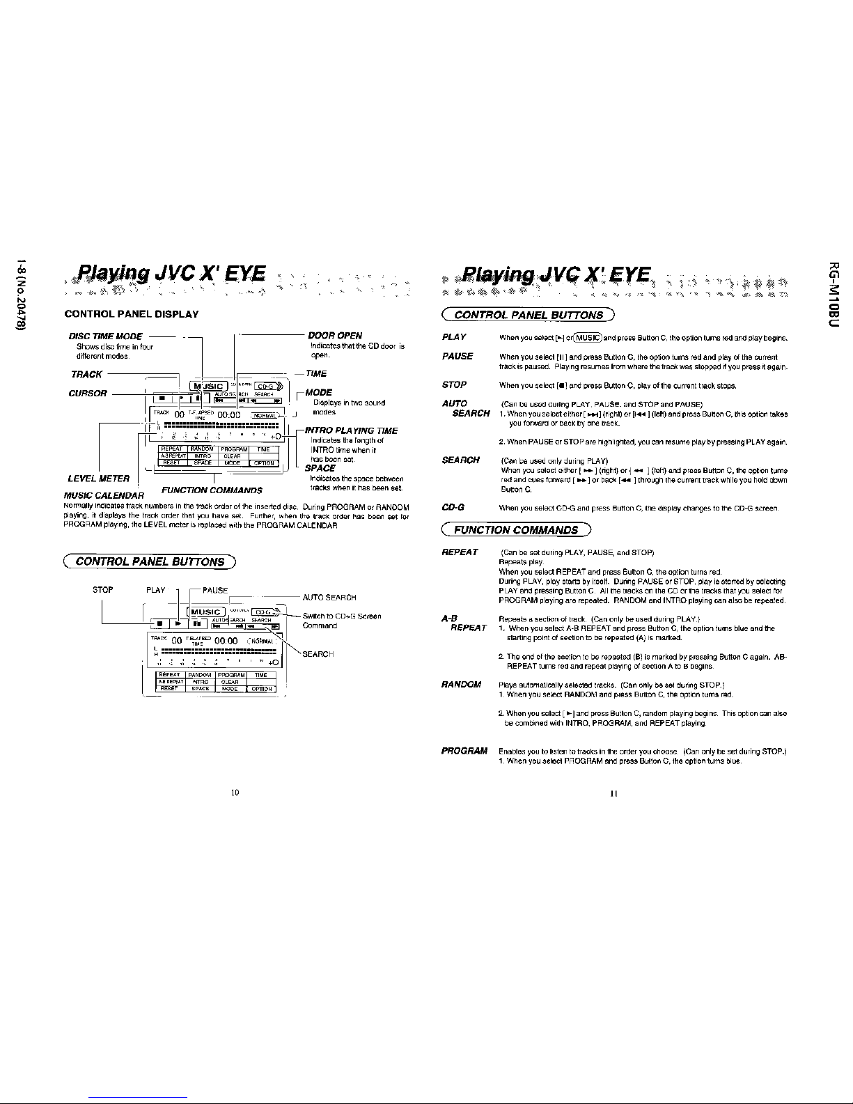
Page 8
,
J'~}flqg
JVC
~·
~YJi
·"'"*';z,ft\
..
·,.
,·""'<>
CONTROL
PANEL
DISPLAY
DISC
TIME
MODE
--
.
1
.
__
Shows disc
time
in
tour
-----DOOR
OPEN
Indicates that
the
CD
door
is
d1fterent
moOOs
open_
TRACK
,--
.___lM'JSIC
1-~
"0~"
I CG-0-
$>
I
-TIME
---~'
7~7~c
"IJ
"''°'c
RC><
sEAAc<
1
MODE
I
~1::...J...!!
r!!C::
'"'1'"'
'""
1
Displays
in
two sout>d
~O
,_,
APSEO
oo-oo
OORMAL-
I J
modes
CURSOR
n~
I
:-~::~°;::::~~=~=~=;===.=~:==:=!~]I
1
l=?t::~;:~~~ME
REP'EAT
R<NDOM
PROORAM
TIME
INTRO
time
when
If
""'"''"'
1'1TRO
CLEAR
has
been
Mt
R<SET
SPACE
MODE OPTION I
SPACE
LEVEL
METER
Indicates the
space
between
tracks
wOOn
it has been set.
MUSIC
CALENDAR
FUNCTION COMMANDS
Normally
1ndicat10S
track numbers
1n
the track order
of
the inserted disc. During PROGRAM or RANDOM
playing,
~displays
the track order that you have set. Further, when the track order has been set for
PROGRAM
playing, the
LEVEL
meter
1s
replaced with the
PROGRAM
CALENDAR
( CONTROL PANEL BUTTONS )
STOP
'~' I ~PAUSE
AUTOSEARCH
-r~USIC
I
00'0
''"~swttchtoCD+GScreen
,~.
~'
-··l
Aiilod;AACH
'""""
I
,-""
l':_j
-~
iiil..,
!fl
Command
"''"'
oo
'~',=
oo:oo
'"o~
I
L
······-··-·····-·-······;!
I~
"
····-••••-••••••-•••••••••••
SEARCH
"
'"+O
REl'EAT
RANDOM
Pf>YJRllM
TIME
A~
REPEAT
l'ITRO CLEllA
RESET SPACE
~OOE
OPTION
'1')
~~404+
%*';,
,,,fiJ&1:1
( CONTROL PANEL BUTTONS )
PLAY
PAUSE
STOP
AUTO
SEARCH
SEARCH
CD-G
When you
se~"1
[~]
or(MUSiC)
and
press
Buttoo
C,
the option turns rad
an<!
play begins.
When you select
[II]
and
press
Button
C, the option turns red arKl play
of
the
currant
track
is
paused. Playing resumes from where thetraci<was stopped
tt
you
press~
again.
WOOn
you select [•J
and
press Button C, play of
the
current
track
stops.
(Can be
used
during PLAY, PAUSE. and
STOP
and PAUSE)
1. When you select
either[-]
(right)
or
['-
I (leH) and
press
Button C, this option takes
you forward
or
back
by
one
track_
2.
When
PAUSE
or
STOP
are
h1ghl1ghled, you can resume play
by
pressing
PLAY
again.
(Can be used ooly during PLAY)
When you select either [ -
l (right)
or
( - ] (left)
and
press
BLJtton
C,
1he
option turns
red and cues forward [ -
J
or
back [-] through the current track while you hold down
Button
C.
When you sale<;!
CD·G
and
press
BLJtton
C,
the display changes to
the
CD-G screen
( FUNCTION COMMANDS )
REPEAT
A-B
REPEAT
RANDOM
(Can
b-e
set
during PLAY, PAUSE, artd STOP)
Repeats play
When you select
REPEAT
artd press Button
C,
the option turns red
During PLAY, play starts by itself.
Duling
PAUSE
or
STOP, play is staned
by
selecting
PLAY
and pressing Button
C.
All the tracks on the CD
or
the
tracks that you select for
PROGRAM
playing
are
repeated. RANDOM and
INTRO
playing can also be repealed.
Repeats a
sect10n
ot
track (Cen only
b-e
used
during
PLAY)
1.
When
you select
A·B
REPEAT
and press Button
C,
the option turns blue end
the
starting point of section
to
be repeated (A)
1s
marked_
2 The end of the section to
b-e
repeated
(B)
is marked
by
pressing Button C
aga>n.
AB·
REPEAT
turns red
and
repeat playing of section A to B begins
P"1ys automa\1cally selected tracks. (Can only be
sa1 during
STOP.)
1
When
you sele"1 RANDOM and press Button
C,
the option turns red.
2.
When
you select
[~]and
press Button
C,
rartdom playing tleg1ns Th1sopt1on can also
be comb•ned
with INTRO, PROGRAM, and
REPEAT
play;ng.
PROGRAM
Enables you to listen
to
tracks in the order you choose (Can ooly be set during STOP.)
1
When
you select
PROGRAM
and
press
Button C,
lhe
optton turns blue
10
ll
"'
"'
'
;;:
-
0
"'
c
Page 9
Playing JVC
X'
EYE
CLEAR
INTRO
SPACE
MODE
2.
When
you
select the track you want
to
hear with the cursor
and
press Button
C,
its
numtler
is
displayed on the MUSIC CALENDAR
(Up
10
99 tracks can be programmed.)
3.
Alter
sel&e11ng a track,
when
you
select
EXIT
and
prass
Button
C,
the
cursor
moves
to
the PROGRAM option. [The PROGRAM option turns
re<l.)
4
WOOn
you seleci
[~]and
press Button
C,
PROGRAM playing begins.
Clears the
PROGRAM
option rCan be used
dunng
PlAY,
PAUSE. and STOP).
When
y<iu
se-.ct CLEAR
and
press
BLJtton
c.
everything
in
PROGRAM
is
erased. To
execute PROGRAM again, stop play
by
selecting
[•land
then carry out PROGRAM
steps 1 to 4. To
clear
when
;n PROGRAM, select EXIT and press
Blllton
C (the
cursor
will move to
PROGRAM)
before carrying out steps for
CLEAR
given above.
Plays the
l>egt~ning
o1
each track m order
(Qin
be used during PLAY, PAUSE, and
STOP)_
The
beginning section (introl to be played can be from 1
to
59 seconds.
1_
When you
9"lect
INTRO and press Button
C,
the option turns red
a~d
INTRO
time
1s
displayed
on
the screen_
2 INTRO
t'ma
is ciiengod with the direction blJttons. The right and lelt blJttons are
to
select e<therthe on0s
or
tens
d1g1t
and the up
and
down
buttons are to increase
or
decrea%' tho number
3
When
Button
C"
pressed
:o
end
time setting, the
INTRO
time display disappears.
Duri~g
PLA'f,
piaystarts
by
itself
Du11ng
PAUSE
or
STOP, play is sta'1ed
by
selecting
PLAY
a~d
pressing Button C
Pauses
tor a number
of
seronds
between tracks (Can be used during PLAY, PAUSE.
eodSTOP)
The pause b-etween tracks
(sparn)
can be from 1 to 59 seconds. This feature can be
combined
w1tt1
lr-..tTRO,
PFIOGRAM, and
REPEAT
playing_
Whe~
you select SPACE
acd
press Button
C,
the op\ion turns red and SPACE time is
dis:ilayed
on
tne screen_
2.
SPACE time
1s
c~anged
wit~
the direction bultons
Ti'a
right
a~d
left buttons
a'e
to
select
e:therthe
ones
or
tens digit and the up
and
dowo
buttons are to increase
or
der.reasa 1"0
r~•~rer_
3
When
you pcess B·Jtton C to
end
time setting, the SPACE time display disappears
Du~ng
PLAY, play starts
by
itself
Is
used
fO' the
ocaraoke
funciion
When
yo~
select
MODE
and
press
BLF.too
C,
the following sound modes
ere
displayed.
The
mode
changeo each
t'me
you press Button C
NORMAL'"
l~r
oormal steren soono.
V-MASKING 1s fo• lowerir.g the vo.oo
of a vocalist on a normal
music
CD and to anioy
KaraoKe
by
s1ng1ng
along.
When you
use
Karaoke Disc, please
set
to
NORMAL
position.
"
Pla~g
.JVC X' EYE
TIME
RESET
OPTION
BLIND
CONTROL
11
you select
TIME
and
press the Button C
dunng
playback, the modes below will
be
displayed
The
mode
changes each time you press the blltton.
ELAPSED:
Time
that has passed since
t~e
current track started playing_
T-ELAPSED. Total
time thal
has
passed since the disc sterted playing.
REMAIN
Time
remain•ng
in
the current
tree~.
T-REMAIN Total time remaining on
tl;e
disc_
Turns all function
commands
otf_
When you select
RESET
and press Button
C,
all the function commands
tllat
are
<>r
(those highlighted
1n
red) are
t~rned
off_
Is
selected
when
you want to
beck
up your data or use
op11ooel
1unc!1ons
thill
w'I.
be
available later.
When you select OPTION. the oplional
tur>et1on
semen
appea~
It
is possible to control audio CD playing Without turning on your
TV
Cont•ol funel ono
can
be executed while holding
down
the
START
button
START+
Button
A.
STOP
START+
Button
B·
PLAY
START+
Buttor
C.
PAUSE
START+
d1rect<on
button
(rig~Uleft)
AUTO
SEARCH
(foiward
or
reverse)
PLAYING
CD+Gs
lr•e'1 a CD+G
me
d<sc
tray and close the
CD
door.
2.
Press
START
on the control pad
or
press button
C.
The
CD+G
beg•ns
p!ay1ng
and
the screen goes alJtomahcally to the
CD+G
display
3_
Control during Play is ca
med
olJt
witr
the
CD+G
Control Panel
Press Button
Bon
t~e
control
pad
to
h<de
or
restore :r.e
CD+G
Cortro!
Panel. {With every other toggle, e status
ii~e
appears
on
the CD+G
screen)
Page 10
What
is
a CD+G?
Since a CDTG contains
not
only signals for sound, but also signals
for graphics. you can play still pictures
and cMracters along
with the
music
•
A
disc
may
contain
up to 15
graphFcs
channels
and by
sw1tch1ng
channels, you can
choo"e
different
languages
(e
g Japanese
or
French)
lor
a song's
lyrics Whothar possible
or not
dapands
on
the
disc
so
pleaS<l
read
the instructions
ol
the
disc_
·As
with audio
CDs,
you can control CD+G playing with the
Control Panel
(CD+G graphics are hidden
when the Control Panel
is
being
displayed
J
-
You
may
see
d1stort1on
1n
the
picture after
you cuo
forward or back
wrth
the Control Panel
dunng
PLAY
and return to
the
CD~G
graphics.
(
FUNCTION COMMANDS
) [
--
~~~a~~~eLgraph1cs
channel that
you
TIME
___
____
_
-,
select
with Channel
Select
TRACK
NUMBER
-<'1
1
'".
.~.
1
~1-
MODE
.
1 1
Fnables you
to switch the
sound
modo_
PLAY
------'-J
,-----'-
EXIT
STOP
----
I Takes
you
oack
to
the
Control Panel.
I
~'i''i"i
PAUSE
AUTO
SEARCH
I
'1
'~
'""''i"'"
I
CHANNEL
SELECT (CH)
-L_
J
You can change
the
graphics channel
by
sclac!lng
a
desired channel
with
the
direction
buttons and
pressing Button
C_
(You
can
choose lrom
15
channels
J
Mic Mixing (Singing
along
with the music.)
1 Connect the microphone to
tho oonscle
2.
Adjust microphone
volume
~~--J
jl=,~-'<
----1
Microphone
volume
The microphone
1s
plugged
IS
adjusted with
MIC.
into the
MIC
Port
(MIC)
R
'
R•
R
*
*'
*
*
'
'
The
vocal
masking
(V-MASKING)
----.
Lowers the volume
of the smger's voice
on
audio CDs
Select MODE and press
Button
C.
then
select
the
V-MASKING
Control Panel.
·What
is
vocal
masking?
I
MUSIC
I
~
[!
_[
U!!J
1~
0
'"~
1
'1.!°'""
....
1
'',;'.,','"' 00:08
,-v-.,..s•iNo'
:::;;::::.-::::::::=::::=
.
.
'
.
. .
,,
"
,.
'
.,
REeFAT
'AN"!~
e<(:2_'A"
'IME
AORro:<T
''°"'
<~°'"
By
lowering tho sound in the
central
pos1t1on
of music
recorded
in
stereo. you can reduce the
volume of
the Stnger's
voice. However. the
voc:al
masking does
not mute
lhe smger's
voice_
Please play music
recorded
1n
stereo
when using the
vocal
mask1n·;i.
If
1t
1s
used
with
mono<a1I
recordings
the
volume of
both ·he singer's voice and
the
muS1c
will
be
reduced
However,
the
vocal
masking may not work even with stereo
revordings
of
ciass1cal
pieces. songs with
few
instruments. duets. songs with strong
echoing
(such
as
chorus pertormances), songs where the singers
voice
1s
not
1n
the
central posit•on.
etc
SOME ADVICE·
---
·You
may exporionca howling
(a
sharp
screeching
noise)
when you
turn
the
microphone
volume
all
the
way
up
To
prevent
this:
1.
Do not face the microphone
toward
the
speakers
or keep the microphone
a
d1s1ance
from the
speakers.
2 Turn down MIC volumo
Tum the
volume down when
not
using
the
microphone
15
"'
G\
'
s
~
0
"'
c
Page 11
z
0
~
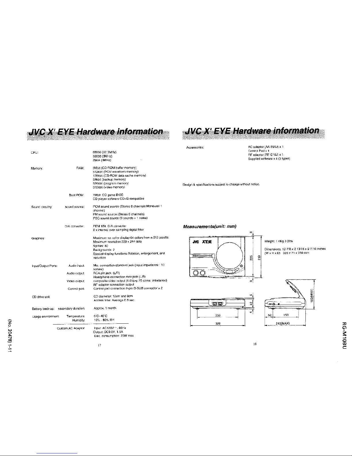
CPU-
Memory
RAM_
8001
ROM
Sound circuitry
Graphics·
lnpuVOutput Ports: Audio inPu\.
Audm
output
V•deo output
Control
port
CD drive
un~
Battery back-up: secondary duration.
Usage
environment
Temperature
Humuj1ty;
Cu"tom
AC
Adaptor·
68000 (
12
5MHz)
68000
(BMHz)
zaoA
(4MHzJ
6Mbtt (CD,ROM
~uHar
memory)
512kblt (PCM
waveform
memoryi
128~b1t
(CD-ROM
da1a
cache
mamory)
64kbit (backup
memory)
576kb1t
(program
memory)
512kbl1 (video
memory)
TMb1!
CD
gamo
BIOS
CD
player saftwam
CD+G
compatll>le
PCM sound source (Stereo 8
channels Monaural I
cnanrial)
FM
soum!
sour"'
(Starao 6 channels)
PSG 50und source
(3
sounds+
1
noo'se)
PEM1Bt!
o.-Aronvcrter
Bx
1ntem~l
ovor-sam~lng
dogttal
Jilter
Maximum
no.
color
d1•play
84
colo"l
from
a 512 palette
Ma.,mum
resolu!ion;320 x 244 dots
Sprites·
SO
Backgruunds 2
Sp~c•al
d1~ay
funC1ions
Rotattro,
enlargement,
and
raducuon
Mii: connecuon W\n<:!;lrd jack
(lnplll
lmJl<ld6ncG
:
1
0
kohrns)
RCA p;n
1a~k
{UR)
Headphone
comJeciton
m1rn-jack
{L'fl)
composite video output
(1
ovp-p
75 chms:
tmtJal~nce)
RF
adaplor connsctron
output
Control
pad
connoct•on 9-p•n D-SUB connocior
x
2
CD
d1amoto•-
12cm
and
Scm
Access ttme-
t\vemge
O
8
sac.
Approx.
1
month
O'C·
40'C
10°io-80%RH
Input
AC120V~',
60Hz
Ol11put DC9.5V,
1 5A
Elec
consumption
WW
max
AC
adaptor (AA-895.J) x
1
Contn;il Pad
x
1
RF
adaptor {RF-S10JI x
1
Suppli~d
software x
4
(3
types)
Design
&
spec1llcatlons
subject
lo
change
wrthout
nouce.
Measurements(unit:
mm)
.m:
"""
\
"'
/o
00
-~:-;_
__
.
/:---
.
I
!
-----...;
••
i
'
•
"
•
~
_l
Weight.
1
4Kg
3
21hs
Dltnl'll1S!Ofl~-
12
7.-lj
x
113/1
6
x
9
7.'16
;r>C(1es
(WxKxD)
320x71x239mm
~-~---=
ii
[:'
'~l:;,_J
-
0
"'
c
Page 12
RG-MlOBU
Jnescription
of
ICsJ
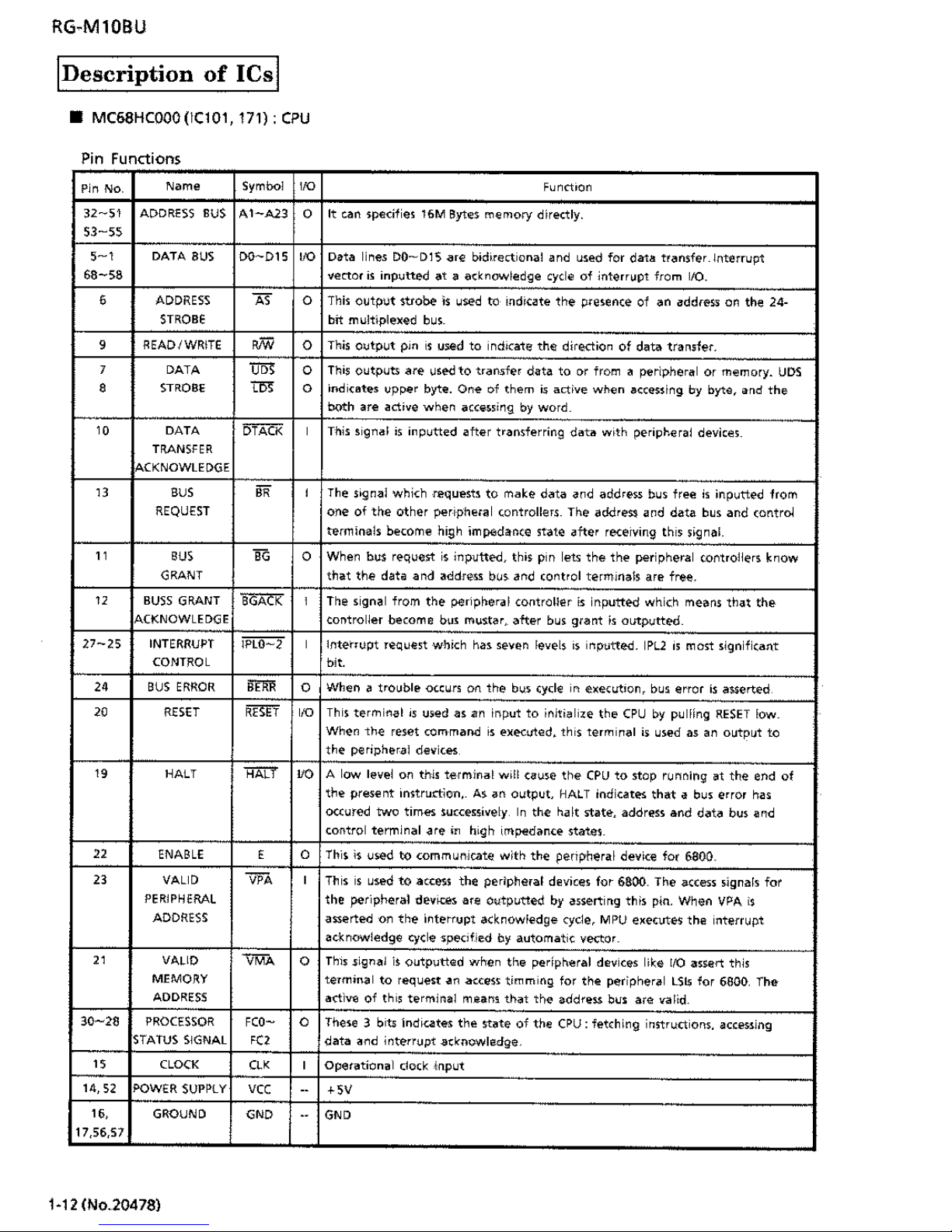
• MC68HC000(1C101,
171):
CPU
Pin
Functions
Pill
No.
Name
Symbol
""
Function
32-51
ADDRESS BUS
A1-A23
0
It
can specifies
16M
Byt~
memory
d'1rectly.
53-55
,_,
DATA
SUS
D0-015
""
Data
lines
D0-015
.are bid.,ect1onal arid
used for
data
transfer.Interrupt
68-58
vector
is
inputted
at
a
acknowledge
cycle
of
interrupt
from
1/0.
6
ADDRESS
AS
0
This
output
strobe
is
used
to
indicate
the
presence
of
an
addres:s
on the 24-
STROBE
bit
multiplexed
bus.
9
READ/WRITE
RfW
0
This O>Jtput
pln
1s
used
to
1nd1Cate
the
direction
of
data
transfer.
'
DATA
uoS
0
This
outputs
are
used
to
transfer
data
to
or
from
a peripheral
or
memory.
UDS
'
STROBE
m:
0
ind1<etes
up~r
byte.
One
of
them
is
active
when
accessing
by
byte,
and
the
both
are
active
when
accessing
by
word.
'°
DATA
DTACK
'
This
signal
is
inputted
after
transferring
data
with
peripheral devkes_
TRANSFER
ACKNOWLEDGE
B
BUS
"
'
The
s•gnal
whkh
raquests
to
make
data and
address
bus
free
is
inputted
from
REQUEST
one
of
the
other
per1phe1al controllers_
The
addre$$
and data
bus
and
<ontrrn
terminals
become high
impedan<e state
after
recerving this
signal.
"
BUS
BG
0
When bus requert
is
inputted,
this
pin
lets
the
the
peripheral controllers
know
GRANT
that
the
data and
address bus
and
control
terminals
are free.
"
BUSS
GRANT
BGA:Ci(
'
The
signal
from
the
peripheral
controller
is
inputted
which
means
that
the
ACKNOWLEDGE controller
become
bus
mus.tar,
after
bus
grant
is
oLJtp"tted.
27-25
INTERRUPT
IPL0-2
'
Interrupt
request
which
has
seven
levels
•s
inputted.
IF'L2
1s
mo>!:
sign'1ficant
CONTROL
bit.
24
BUS
ERROR
""'
0
When
a
trouble
occurs
on
the
bus
cycle
1n
execution,
bus
error
is
asserted
20
RESET
mrr
"°
This
terminal
•s
used
as
an
input
to
initial1ie
the
CPU
by
pulling
RESET
low.
When
the
reset
commaM
1s
executed,
this
terminal
i>
used
as
an
output
to
the
()€ripheral devices
"
HALT
HALT
"o
A
low
level
on
this
terminal
wdl
cause
the
CPU
to
stop running
at
the
end
of
the
present instruction,_
As
an
output,
HALT
indicates
that
a
bus
error
has
oo:ured
tw<:J
times
SU(cessively
In
the
h.alt state,
address and data
bus
and
control
terminal
are in h•gh impedance states.
22
ENABLE
E
0
This
is
used
to
communicate
with
the
penpheral
device
for
6801)_
23
VALID
'PA
'
This
1s
used
to
acces1
the
peripheral devices
for
6800. The
aCCe5s
signals
for
PERIPHERAL
the
peripheral
dev~
are
outputted
by assert1rig
this
pin. When
VPA.
is
ADDRESS
asserted
on
the
interrupt
acknowledge cycle,
MF'U
executes
the
interrupt
acknowledge cycle specif,ed by
automatic
vector_
"
VALID
'MA
0
Th1s
5ignal
is
outputted
when
the
peripheral devices like
1/0
assert
this
MEMORY
terminal
to
request an
access
timm1ng
for
the
peripheral
LS"5
for
6800.
Th•
ADDRESS
activa
of
this
terminal
mearis.
that
the
address
bus
are
valid.
30-26
PROCESSOR
FCO-
0
These
3
bits
1nd1cate-s
the
state
of
the
CPU: fetching ins-truct1oris. accessing
STATUS
SIGNAL
ec2
data
and
interrupt
-atknowledg-e,
,,
CLOCK
'"
'
Operational
clo~k
input
14,
52
POWER
SUPPLY
"'
--
""
"-
GROUND
GNO
--
GNO
17,56,57
1·12CNo.20478)
Page 13
RG-M10BU
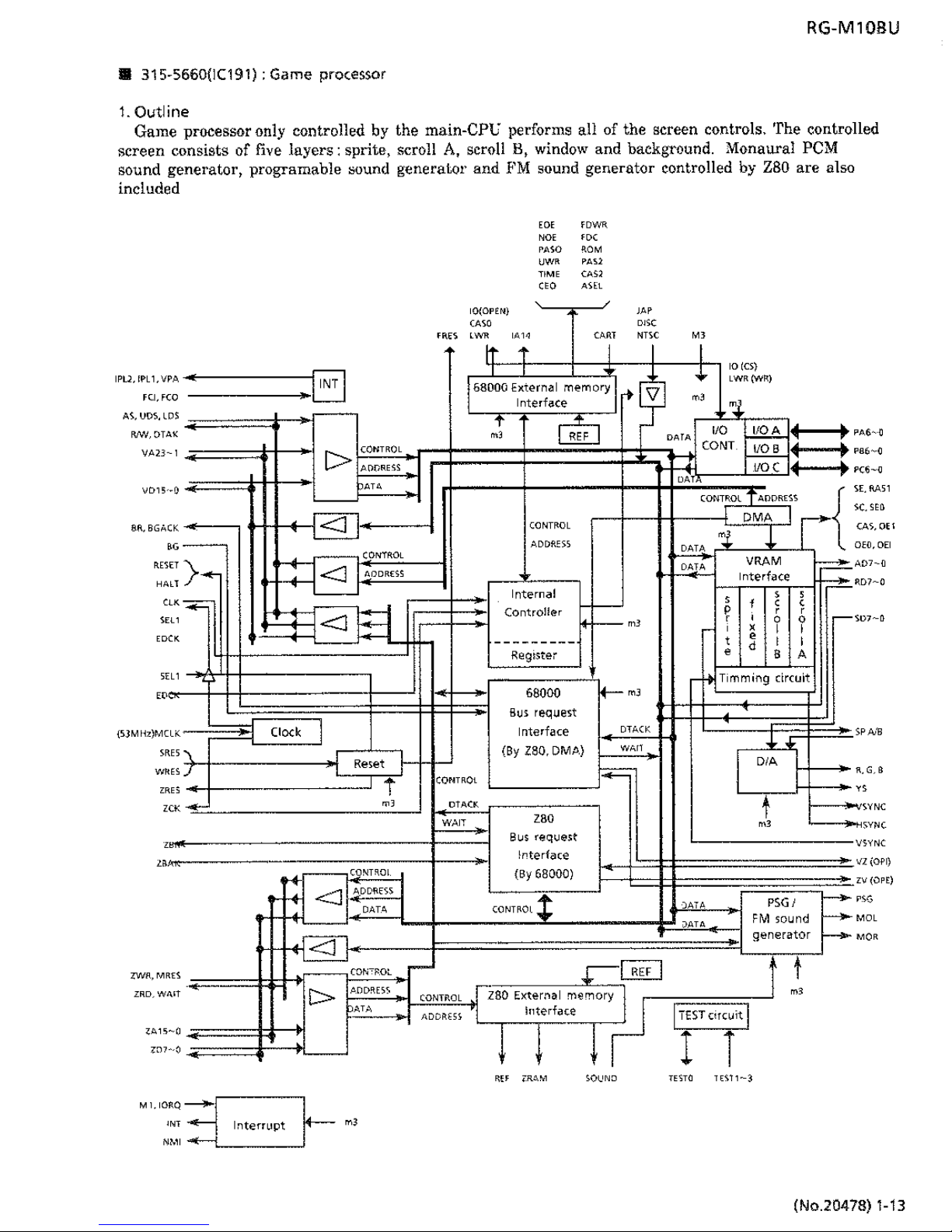
• 315-5660(IC191):
Game processor
1.
Outline
Game processor
only controlled by the main-CPL"
performs all of the screen
controls,
'rhe controlled
screen consists of five
layers:
sprite, scroll
A,
scroll
B,
window and background. Monaural
PCM
sound
generator,
prograrnable
:;ound
generator
and
f'M
sound
generator
controlled by Z80
are
also
included
IPLl,IPL1,V
"
w
F<:.I,
f
AS, UOS,
l
RN/,
OT
VA23
°'
"
_,
V015
_,
BR,
BGA
"
"'
•
ET)-.+
"
"=i
"
rn
"
"
"
{SJMHz)MC
'"
'"
,,,
"
"
-
?;WR,
MR
"
ZRD,WA
"
·~
-o
- 0
-
~
-
'
Clock
6
I>
CONTROL
AO{)RE'iS
'"
<l
(Or<TROL
<::::]
I
ADDRESS
-
<lH
I
Reset
t
"'
CONT~OI
<l
~DRESS
DATA
<l
CON
·~OL
C>
AODRE5S
PATA
Ml,IORQ~
'"'
Interrupt
m3
NMI
rn'
fDW~
"°'
"'
PASO
""
"we
PAS2
TIME
CASl
Orn
ASll
IQ(OPEN)
'"
CASO
DJS(
'"''
'~
IA14
CART
NTSC
It
1"
I
'
!
68000 Einernal
memory
lnterf«ce
+
v
'
~
,,
CONTROL
ADDRE>I
lntern<1I
Controller
"'
~
---------
Register
68000
,_,,
Bus
request
Interface
DTACK
{By
Z80,
DMt>.)
WArl
[QNTR0l
f=;
DTACK
WAIT
rnD
Bus
request
i~terface
(By
68000)
CONTROL
I
-
.r-~
CONTROL
ZBO
External
m€rnory
A0DR'51
, I
Interface
I
l
j
10L'ND
"'
I
+
10
ICS)
LWR (WR)
,,
'
"o
l!OA
DATA
CONT
1/0
B
00(
"
.
'
~
~
'
~
~
'
A6,U
so-o
C6-0
.RA51
{"
CONTROL
D~;OR£:S
r·
S
'I
I
0
C.
SEO
CAS,O!l
EO,
OEI
07-0
DATA
DATA
"'-'M
Interface
,
f
'
f
' '
p
' '
'
'
0 0
'
'
I I
f
'
I I
d
'
B
A
T1mming
circuit
j_
D"
t
"'
)ATA
PSGI
JATA
FM
sound
-
generator
I
"'
I
TEST
cncuit
I
l
T
TEITO
TE\11-3
=·
'
~·
'
•
•
SYNC
'
'.<YNC
SYNC
l(OPI)
V (OPE)
'
'
•
f-,.M
f-,.M
(No.20478) 1-13
Page 14
RG-M10BU
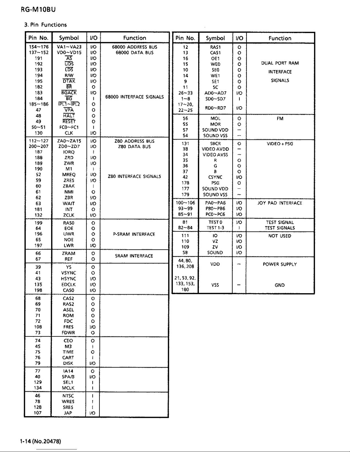
3.
Pin Functions
Pin
No. Symbol
1/0
Function
Pin No.
Symbol
1/0
Function
154-176
VA1-VAZ3
VO
68000
ADDRESS
BUS
"
RA51
0
137-152
VOO-VD15
VO
68000
DATA
BUS
13
CAS1
0
191
AS"
1/0
16
OE1
0
192
DOI
110
15
MO
0
DUAL
PORT
RAM
193
cos
1/0
10
SEO
0
INTERFACE
194
-
110
"
WE1
0
195
DfAK
110
9
SE1
0
SIGNALS
182
"'
0
11
SC
0
183
BGA(k
1/0
26-33
AD0-AD7
1/0
184
T<l"
I
68000
INTERFACE
SIGNALS
1-8
SDO-SD7
I
185-186
Wli-Tm
0
17-20,
47
VPA
0
22-zs
RDO-RD7
110
48
Hm
0
"
MOL
0
FM
"
=
0
SS
MOB
0
S0-51
FCO-FC1
I
57
SOUNDVDD
-
130
CLK
1/0
S4
SOUNDVSS
-
112-127
ZA0-ZA15
1/0
ZSO
ADDRESS
BUS
131
SBCR
0
VIDEO+PSG
200-207
ZD0-207
1/0
zao
DATA
SUS
"
VIDEO
AVDD
-
187
IORQ
I
3'
VIOEOAVSS
-
188
"'
1/0
lS
8
0
189
ZWR
1/0
36
G
0
190
M1
I
37
8
0
"
MREQ
1/0
ZSO
INTERFACE
SIGNALS
"
(SYNC
1/0
"
ZRES
1/0
178
PSG
0
60
ZBAK
I
177
SOUNDVDD
-
61
NMI
0
179
SOUNDVSS
-
"
ZBR
110
63
WAIT
1/0
100-106
PAO-PA6
llO
JOY
PAD
INTERFACE
181
INT
0
93-99
PSl.l-PB6
VO
132
ZCLK
1/0
85-91
PCO-?C6
1/0
199
RASO
0
"
TESTO
1/0
TEST
SIGNAL
"
eoe
0
82-84
TEST
1-3
I
TEST
SIGNALS
196
UWR
0
P-SRAM INTERFACE
111
10
VO
NOT
USED
6S
NOE
0
110
vz
1/0
197
LWR
1/0
109
zv
110
66
ZRAM
0
58
SOUND
1/0
67
REF
0
SAAM
INTERFACE
44,80,
136,
208
VOD
-
POWER
SUPPLY
39
YS
0
41
VSYNC
0
"
HSY
NC
VO
21, 53. 92.
135
EDClK
1/0
133, 153,
vss
-
GNO
198
CASO
1/0
180
68
CAS2
0
69
RASZ
0
70
ASEL
0
71
ROM
0
7Z
fOC
0
"'
fRES
llO
73
FOWR
0
74
CEO
0
"
Ml
I
"
Tl
ME
0
76
CART
I
79
DISK
1/0
77
IA14
0
40
5'A/8
1/0
1Z9
SEL
1
I
134
MCLK
I
46
NT"
I
"
WRES
I
1Z8
SRES
I
107
JAP
llO
1-14(No.20478)
Page 15
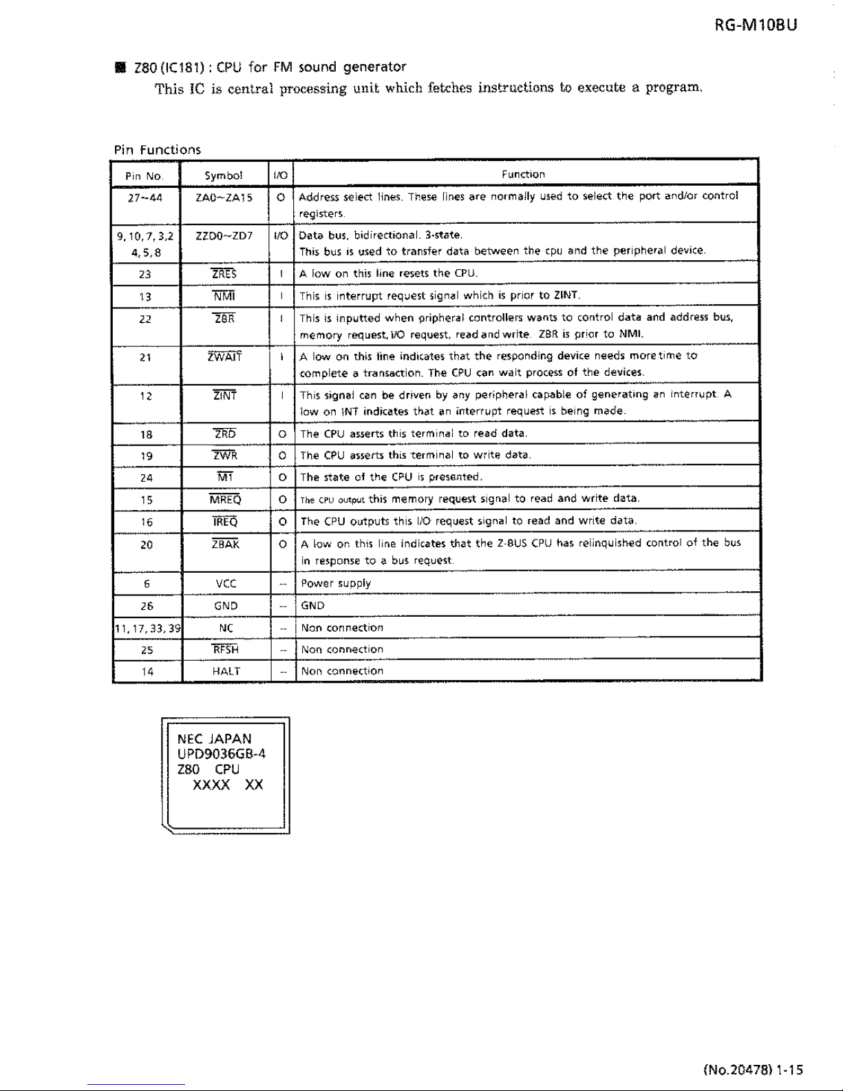
RG-M10BU
•
Z80
(IC181):
CPU
for
FM
sound
generator
This
IC
is
central
processing
unit
which fetches instructions
to
execute a
program,
Pin
Functions
Pin
No
Symbol
27-44
ZAO-ZA15
9,10,7,3,2
ZZDO-ZD7
4,
5,B
"
ZRES
"
NM'
2'
ZBR
"
ZWAl'r
"
ZINT
"
WD
"
'WR
"
M'
'5
MREQ
'6
IREQ
'°
ZBAK
6
vcc
"
GND
11,17,33,39
"
"
"
RFSH
HALT
NEC
JAPAN
UPD9036GB-4
ZSO
CPU
xxxx
xx
"o
Function
0
Ad<Jress
S€iect
lines_
Tnese lines
are
normally
used
to
select
the
port
a~dlor
control
regirters
"o
Data
bus.
bidirectional_ 3-state.
This
bus
is
used
to
transfer
da~a
between
the
cpu
and
the
peripheral device.
'
A
low
on this
l<ne
resets
the
CPU_
'
This
1s
interrupt
request signal
which
is
prior
to
ZINT.
'
This
IS
inputted
when
jlripheral
controllers
wanU
to
control
data
and address
bus,
memory
request.
l/O
request,
read and write
ZBR
is
prior
to
NMI.
'
A
low
on
this line indicates
that
the
responding device
needs more
time
to
complete
o
transoction_ The
CPU
can
wait
process
of
the
devices.
'
This
signal
can
be
driven
by any
pe1ipheral capable
of
generating
an
Interrupt
A
low
on
\NT
indicates
that
an
interrupt
request
1s
being
made.
0
The
CPU
as.serts
this terminal
to
read data.
D
The
CPU
asserts
thLs
terminal
to
write
data.
0
The
state
of
the
CPU
11
presented.
0
The
CPU
outptJt
this
memory
request signal
to
read
and
write
data.
0
The
CPU
outputs this 1/0
request
signal
to
read and
wnte
data.
0
A
low
on
this line
indicates
that
the
Z-BUS
CPU
has relinquished control
of
the
b"
in
response
to
a bus request
Power supply
GND
i
Non connection
Non
conri;oct1on
Non
connection
(No.20478) 1-15
Page 16
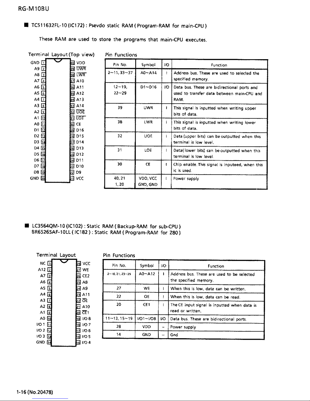
RG-M10BU
• TC511632FL-10 (lCl
72):
Psevdo
static RAM (Program-RAM
for
main-CPU)
These
RAM
are
used
to
store
the programs
that
main-CPU
executes.
Terminal
Layout (Top
view)
Pjn
Functions
GNO
VDO
A9
·-
A8
LWR
Pin
No.
Symbol
•D
function
2-11,33-37
AO-A14
'
Addres.s
bus.
These are used
to
wlected
the
A7
A>O
spedfied memory.
AG
A11
12-19,
Dl-016
<IO
Data
bus.
These
are bidirectional
P-Orts
and
AS
A12
22-29
used
to
transfer
data
between
ma'1n-Cf'U
and
A4
Ml
RAM.
Al
A14
A2
Dl5E
39
UWR
'
This srgnal
is
inputted
when
writing
upper
bits
of
data.
"
CE
38
lWR
'
Thi$ signal
is
Inputted
when
wrtting
lower
03
036
bit;
of
data.
02 035
"
UDE
'
Data (upper bits)
can
be
outputted
when
this
03
DH
terminal
;s
low level.
o•
on
"
LOE
'
O..ta{
lower
bITTl
'ari
be
outputted
when
this
05
012
terminal
is
low
level
06
011
07
30
CE
'
Chip enable.
This
signal
is
inputeed, when this
08
09
i~
is
E.l~d
GNO
VCC
41),21
VOD.
VCC
'
Power supply
1.
20
GND,GND
• LC3564QM·10 (IC102)
:
Static
RAM
(Backup-RAM
for
sub.CPU)
BR65265Af-10LL
(
!C182):
Static
RAM
{Program-RAM
for
280)
Terminal
Layout
Pin
Functions
NC
vcc
Pin
No.
'Symbol
•D
Function
A32
'
WE
A7
CE2
2-10.i1.21-·~
A0-A12
'
AddreS'S
bus.
These are
u~ed
to
be selected
A6
AS
the
specrf1Eld
memory.
AS
A9
27
we
'
When this
is
low,
data
can
be
written.
A4
A11
22
OE
'
When this
is
low,
d<1ta
can
be
read.
Al
"'
A2
1
A10
A3
""1
20
{E1
'
The
CE
input
si>gl"lal
is
inputted
when
data
is.
read
or
written.
M
me
11-13,
15-19
1/01-1/08
l/O
Data
bus.
These are bidirectional
ports.
"'"
"'"
28
YOO
-
Power
supply
"'"
"'"
"'"
10
5
"
GND
-
God
GNO
1104
1·
16
{No.20478)
Page 17
RG-M10BU
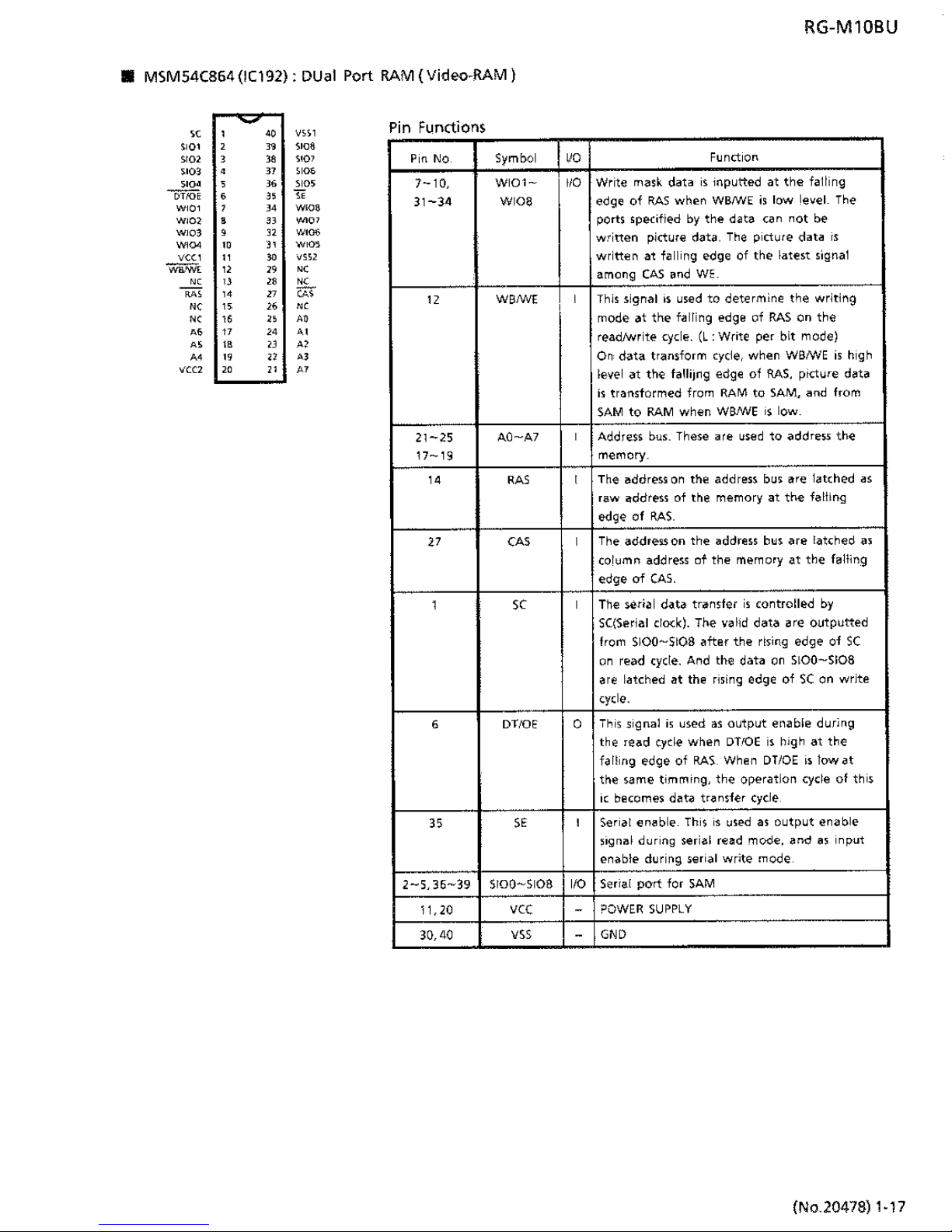
• MSM54C864
(IC192):
DU
al
Port RAM {
Vide-0-RAM)
"
"
VII
1
Pin Functions
1101
"
s1oa
1102
'"
S•07
Sl03
H
;,m
Prn
No
Symbol
VO
Function
110•
"
5105
[)'i'iill
•
"
"
Wl01
"
wo•
7-10,
WI01-
VO
Write
mask
data
11
1nputted
at
the
falling
31-34
Wl08
edge
of
RAS
when
WBNIE
is
low
level.
The
WJ02
•
"
~"
ports specified
by
the
data
can
not
be
WJ03
"
w'~
w'~
"
"
WIOS
written
picture data.
The
picture
data
rs
VCC1
"
"
VSl2
\iiiiiNil[
" "
"
"
"
''
"
written
at
falling
edge of
the
lat<est
signal
among
CA5
and
WE_
"'
"
n
CAf
"
"
"
"'
"
WBN/E
'
This
sigrral
1s
used
to
determine
the
writing
'
"'
" "
"
"
H
"
"
" "
"
M
mode
at
the falling
edge
of
RAS
on the
readi\Nrite cyde.
(L:
Write
per
bit
mode)
M
w
"
.,
VCC2
'"
"
M
On
data
transform
cycle,
when WB/WE
is
hrgh
level
at
the
falli1ng
edge
of
RAS.
picture data
is
transformed
from
RAM
to
SAM,
and
from
SAM
to
RAM
when
WBJWE
IS
low.
21-25
A0-A7
'
Addres>
bus_
These are
used
to
address
the
17-19
memory.
"
'AS
'
The
"ddress
on
the address bus
"re
latched
as
raw
address
of
the memory
at
the
f,.lting
edge
of
RAS.
"
CAS
'
The address
on
the
address bus
are
latched
as
column address
of
the
memory
at
the
falling
edge
of
CAS.
1
SC
'
The
wrial
data
transfer
is
controlled
by
SC(Serial clock).
The
valid
data
are
outputted
from
SIOO-SIOS
after
the
rising edge
of
SC
on
read
cycle.
And the data
on
5100-SIOS
are latched
at
the
rising
edge
of
SC
on
write
cycle.
'
DTIOE
0
T~1s
signal
is
used
as
output
enable
during
the
re11d
cycle
when
DTIOE
1s
h•gh
at
the
falling
edge
of
RAS
When
DTIOE
1s
tow
at
the
same
timmmg,
the
operation
cycle
of
this
1c
becomes data transfer cycle
3;
SE
'
Serial eflable. This
1s
used
as
output
enable
11gnal
during
serial
read mode.
afld
as
input
enable
during
serial
write
mode
2-5,36-39
5100-5108
'IO
Serra!
port
for
SAM
11,20
"'
-
POWER
SUPPLY
30,40
'"
-
GND
(No.20478)
1-17
Page 18

RG-M10BU
• HD404019RC23FS(IC691)
CD
controller
1.
Terminal
Layout
HD404019
"
20
52
51
33
32
2.
Pin
Functions
Pin
Symbol
No.
uo
Function
T
oCD
0
'
DSPM
0
Mutinn
signal
for
audio sinnal
3
MONO
0
'Vrnce
changer','L-di'.'R-ch'
:
High
4
VCAN
0
'Vocal mask1m;{:HiQh
5
VCHN
0
'Voice
changer';
H1cih
6
L
0
'Normal';Vocal
ma~kino','L...;h':
High
T
R
0
'Normar
;vocal
ma~kin1,j',
'R-ch ·
:
High
8
--
Non
connectt-On
9
-
Non
connection
10
..
Non
connect•on
"
Non connection
32
..
Non
connection
n
GNO
--
Ground
'4
ERES
'
Reset si9nal
for
IC141
'5
HOCK
0
"
SCOR
'
Detect
the
ar~arance
of
sync.
of
subcode
"
WfCK
'
Not
used
18
D80
'"'
Communication
data
wrth
sub-CPU
"
DBl
uo
Comml'n1cat1on
data
with
sub-CPU
20
DS2
'"'
Communication
data
wrt:h sub-CPU
23
D"3
uo
Communication
data
with
sub-CPU
22
COCK
0
Clock
out
to
communicate
with
sub-CPU
23
"O
O
Interrupt
raquert
si<:uial
to
sub-CPU
"
DMUTE
0
Mutfng
si
nal
for
"Serch'
and
'Pause'
'5
D/M
0
CO-ROM : H,
Audio
disc:
l
26
vcc
-
Power
supply
27
SQCK
0
lock
out
to
rea<J
SQSO
28
SQSO
'
data
of
sulx.ode
is
inputted
29
DATA
0
Control
data
for
O:D2500BQ
30
CLOCK
0
Cl<XkfortranrlorminQ
DATA
31
CLOSE
SW
'
Detect
the
disc
door
dos1no
32
Not
used
(Non
connectiOll)
1-18 (No.20478)
Pin
No
Symbol
11/0
Function
B
-
Not
used
(Non connection)
34
-
Not
used
(Non connection)
3S
-
Not
use-d
{Norr
cor>nect1on)
36
-
Not
used
(Non connection)
37
-
""
Not
u;ed
(Non connection)
"
UVE
..
Not
u;ed (Non connection)
39
PANOSW
Not
uoed (Non
conruxtion)
40
..
Not
uwd
{Connected
to
GND)
"
Not
u~
(Connected
to
GND)
42
..
Not
used (Connected
to
GND)
43
"'
'
Resetsigna!
inputted
44
vcc
..
Powe1 supply
"
osc
sdllat1on
terminal
..
05C
-
scillat1on
terminal
47
GND
..
round
"
LASER.
0
H;lawron/L:oft
49
•ex
0
H
:Trackrn9off
so
•LAT
0
Latch
sf-anal
for
CXD2SOOBQ
"
DECT
0
oefectsional
out
52
LOCK
'
Lock signal
input
"
EO'
'
Focus
ok
si
nal
input
54
SENS
'
sense sianal
out
SS
TEST
'
est
mode
termln~I
56
'"'
0
Emphas.i~
control
s1
nal
5'
--
Not
used
{Non connection)
58
..
Not
used
(Non
connection)
59
-
Not
used
(Non
connection)
60
-
Not
used
(Non
connection)
"
'ANO
..
ot
~(Non
connectiOn}
"
-
Not
used {Non connection)
63
..
Not
u~ed
{Non connection)
64
..
Not
used
(Non
connection}
Page 19
RG-M10BU
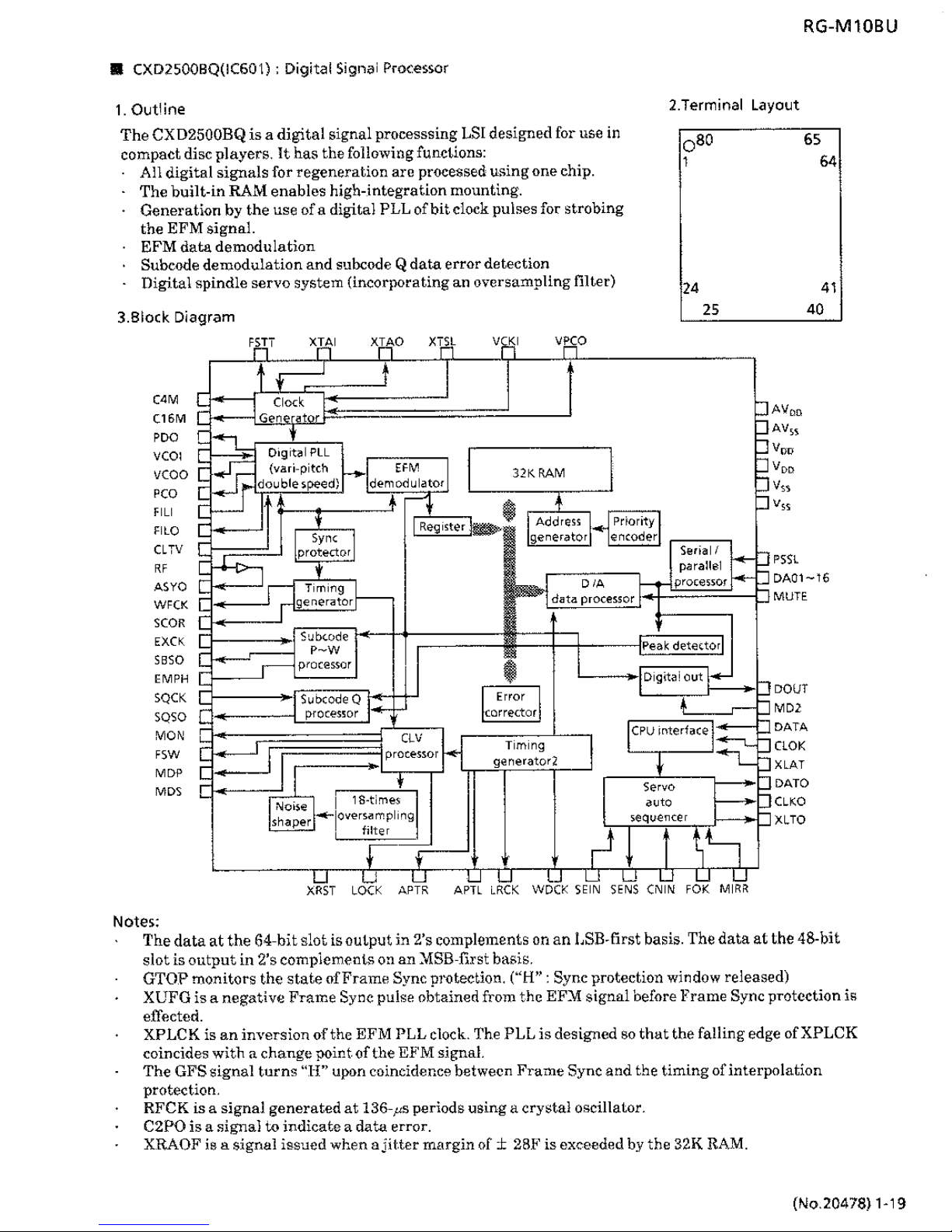
8 CXD2500BQ(IC601):
Digital
Signai
Processor
1.
Outline
2.Terminal
Layout
The
CXD2500BQ
is
a
digital
signal
processsing
LSI
designed for use in
compact
disc
players.
It
has
the follo>ving functions:
All
digital
signals
for
regeneration
are
processed
using
one
chip.
The
built-in
RA!vl
enables
high-integration
mounting.
Generation
by
the
use of a digital
PLL
of
bit
clock pulses for
strobing
the
EFM
signal.
EFM
data
demodulation
Subcode
demodulation
and
subcode
Q
data
error
detection
Digital
spindle
servo
system (incorporating
an
oversampling
filter)
3.Block
Diagram
FSTT
XPil
xPJ"o
XTSL
V)...KI
VPCO
•
I
oBO
1
24
25
"M
C16M
PDQ
VCOI
vcoo
PCO
FI
LI
FILO
CL
TV
ee
ASYO
WFCK
SCOR
EXCK
SBSO
EMPH
SQCK
SQSO
MON
PSW
MOP
MOS
Clock
2:,
Goe
1
'
01g1tal
PLL
~
:.rr:
(vari-pitch
-I,
EFM
32K
RAM
double
speed)
demodulator
I '
I
@ '
i
'
1
Register]D
I,
Address
Priority
Sync
generator
«ncoder
protector
Serial I
k-
2
r
parallel
'
k-
T1m1ng·~
""""
D
'A
processor
~
I
data
processor
I
generator
Sub,ode
P-W
Peak detector!
-
,-
processor
@
~
~
Sut>code
Q
I,
Error
,I
1
processor l.._.
corrector
I
CLV
CPU
interface!--..
c------'
I
processor~
T1m1ng
J
generator<
•
~
•
Servo
Noi>erl·
I
18-time~
auto
'
shaper
..-1over~_ampl1~g
>equ<:>~cer
1lter
'
I
t
I
I
u
u
LJ
I
LJ
c
u u
XRST
LOCK
APTR
APTL
LRCK
\VDCK
SEIN
SENS
(NIN
FOK
MIRR
Notes:
AVon
AV1~
Voo
Voo
v"
v"
65
64
41
40
PSSl
OA01-t6
MUTE
DOUT
MD2
DATA
CLOK
XLAT
DATO
CLKO
XLTO
The
data
at
the
64-bit
slot
is
output
in
2's
complements on
an
LSB-first basis. The
data
at
the
48-bit
slot
is
output
in
2's
complements
on
an
:MSB-first
basis.
GTOP
monitors
the
state
ofFrame
Sync
protection.
("H":
Sync
protection window released)
XUFG
isa
negative
Frame
Sync
pulse obtained from
the
EF:M
signal
before
Frame
Sync
protection
is
effected.
XPLCK
is
an
inversion
of
the
EFM
PLL
clock. The
PLL
is
designed so
that
the
falling edge
ofXPLCK
coincides
with
a
change
point
of
the
E.FM
signal.
The
GFS
signal
turns
"I-I"
upon coincidence between
Frame
Sync
and
the
timing
of
interpolation
protection.
RFCK
is
a
signal
generated
at
136-µs periods using a
crystal
oscillator.
C2PO
is
a
signal
to
indicate
a
data
error.
XRAOF is
a
signal
issued
when
ajit.ter
margin
of±
28.F
is exceeded
by
the
32K RAM.
(No.20478) 1-19
Page 20

RG-M10BU
4.
Pin
Functions
Pin
No.
Symbol
,;o
Function
1
FOK
I
Focus
OK
input
pin.
Used
for
SENS
output
and
servo
auto
sequencer.
'
f'iW
0
Non
connection
3
MON
0
Output
for
spindle
motor
ON
/OFf
control.
4
MDP
0
Output
for
spindle servo control.
s
MOS
0
Output
for
5pindle servo
control
(Non connection).
6
LOCK
0
This
terminal
is
HH
"when
the
GFS
signal
~mpled
at
460Hz
is
"H"
.It
turns
NL"
when
the
GFSs1gnal
turns
out
"L"
8
or
morEtime11n
succession.
,_,
--
Non
conn€ct1on
1D
TEST
I
Test
pin
(Normally
at
OV)
"
PDO
0
Output
of
charge
pump
for
analoo
EFM
PLL
(Non
connection).
12
v
..
--
GND
13-16
Non
connection
"
V(KI
I
Clock 1nput
from
external
VCO
for
van-pitch
control
fc ..
16.9344MHz.
1B
FILO
0
Output
of
filter
for
masterPLL
(Slave~
D191tal PLL)
19
FILI
I
Input
to
filter
for master
Pll.
20
eco
0
Output
of
charge
pump
for
master
PLL
21
AVss
Analog
GND
22
CLTV
I
VCO
control
voltage
input
for
master
PLL.
23
AV
Analog
power
supply
24
"
I
EFM signal
input
25
TEST2
I
TEST
pin
(Connected
to
GND)
26
TEST3
I
TEST
pin
(Connected
to
GND)
"
ASYO
0
EFM
full-swing
output
"
TEST4 I
TEST
pin
(Connected
to
GND)
"
NC
--
Non
connection
30
PSSL
I
Input
use-0
to
switch
the
audio
data
output
mode.·
L"
for
serial
output,"H"
for
parallel
output.
"
WDCK
0
DI
A
interface
for
48·bit
slot.
Word
clock
f'"
2Fs.
32
LRCK
0
D/Ainterfawfor48-bitslot_
LRcloctf.,
Fs_
33
v
Power
supply
34
DA16
0
Output
DA
16{MSB)
when
PSSL"'
1
or
serial
data
from
4S-bit
sloi:(2'1
completements.MSB
first)
when
PSSL"' 0
3S
DOA15
0
Output
DA
15
when
PSSL""
1
or
bit
clock
from
48-bit
slot
when
PSSL
~
0.
36--S
1
Non
connection
52
vss
--
GND
53
XTAI I
Input
to
16.9344MHz
Xtal
oscillation
circuit
or
33.8688MHz
11'\put_
54
XTAO
0
Output
of
16
9344
MHz
Xtal
osc1llat1on circuit_
SS
"'"
I
Xtal
selection
11'\put
pin
"L"
for
16,344MHi
Xtal.
'H"
for
33.8688
MHz
Xtal.
56-58
-
Non
connection
59
MD2
I
Digital-Out
ON/Off
control
"H"
for
ON,
"l"
for
OFF_
60
DOUT
0
Digital-0lJtoutput
pin.
6'
EMPH
0
H:
empha$ts
on
L:
emphasis
off
62
--
Non
connection
63
SCOR
0
Turns
"H"
when
subcode Sync
SO
or
$1
11
detected.
64
saso
0
Sen<1I
output
of
Sub P
tow_
65
EXCK
I
Clock
input
for
reading
SBSO.
66
SQSO
0
Outputs
80-bit
Sub
Q
and
16-bit
PCM
peak
l<i!veldata.
"
SQCK
I
Clock
input
for
reading
SQSO
68
MUTE
I
"H"
for
muting,
"L
•for
release.
69
SENS
0
SENS
output
to
CPU.
'°
XRST
I
ys.tem reset.
"L"
for
re~tting_
"
DATA
I
Inputs
serial
data
from
CPU.
"
"'-'"
I !Latches serial
data
inout
from
CPU
atfallins
edoe.
"
v,,
--
1PoW<i!rsllpply(
+
SV)
"
(LOK
I l11p-utsserial
data
transfer
dock
from
CPU.
7S
SEIN
I lnplJtsSENSE
from
SSP
76
CNIN
I
Inputs
track
1um
p
count
s10
naL
"
DATO
0
Outp-uts;erial
data
to
SSP.
"
XLTO
0
Latches :serial
data
output
to
SSP
atfal1uig
edge.
"
CLKO
0
Outputs
serial
data
tran:sfer
dock
toSSP.
ao
MIRR
I lnr>uts
mirror
sinnal
to
be
used
b"
auto
ie"ue-ncer
when
1umrnno
12"
or
m re tFacks.
1-20 (No.20478)
Page 21

RG-M10BU
• CXA 1372Q (IC502):
RF
Signal Processing Servo
Amplifier
1.0utline
The
CXA1372Q is a bipolar
IC
developed
for
RF
signal
processing
(focus
OK,
mirror,
defect
detection,
EFM
comparator)
and
servo
control.
2. Functions
Auto
asymmetry
control
Focus
OK
detection
circuit
Mirror
detection
circuit
Defects
detection,
counter
measures
circuit
EFM
comparator
Focus servo control
Tracking
servo
control
Feed
servo
control
3.
Terminal
Layout
36
12
25
L_
___
__J
13
4.
Block
Diagram
-
-
-
-
'
'
'
'
" '
;
'
'
'-<>
I
I
I
,l
ti'll
~
·Ill
•
.__
~
"
\
+J
·TTL
f-
,;
t°\
I
1..L
(
t>
~
~
6
b
!)
I
;,.
y
~
~~
-i;'
I
I
(
-
'
I
J_
''
,7
~
0
,_
L
ITI
.~
•
:
·Ill
='=
. L
-
~
·TTL
·llLDATA
REGISTER
·INPUT
SHIFT
REGISTER
"'
•
'
·ADDRESS
DECORDER
~~
'
b
4
·Ill
·OUTPUT DECORDER
-
~
"
'
~
"--'
<.>
...,,.
-,>
FSf_,,
](;
1·2
TM1·7
PS\-3
'
I
·TRACKING
PHAI[
,
I
SET
1--
;
COMPENSAT'ON
"'=
~WINDOW(OMPJ\RATOR
r
~T
Ti
~
+'~
~
I\
·fOCUI
PHASE
COMPARJ\TOR
~
;'_]
J
~
~
0
,J
<0--0"'
o-E
t
0
-
~
~
~
~
:f;>
),-
:p;:::
'
'
'
'
,,
"'
"
'
'
~
"
'
'
;
'
"
'
''
t'l
0
'
'
u
(No.20478)
1-21
Page 22

RG-M10BU
5.
Pin
Functions
Pin
No_
Symbol
""
Function
;
"
'
Input
pin
of
tracking
error
amplifier.
2
TDFCT
'
Capacitor connecting pin
for
tr me constant during
d€fects
3
ATSC
'
Window
comp<1rator
input
pin
for
ATSC
det«'ctton_
'
'2(
'
Pin
for
focus zero-cross comparator
inpu"\.
5
FC
'
Input
pin
of
focus
error.
6
FDFCT
'
Capacitor
connecting pin
for
time
constant
during
defect
fu~ctions
'
"
'
Center voltage
input
pin_
for
dual
power:
GND
For
single
power
1upply:
(VCC
+
GND)12
8
FGD
'
Connect
a capacitor between
this
pin
<ind
p1n3
to
reduce high-frequency
gain_
9
CS3
'
The
high-frequency
gain
of
the
focus servo
is
switched
through
FS3
ON
and
OFF_
'°
"'
'
Time constant
external
pin
to
raise
the
low
bandwidth
of
the
focus servo
;;
FED
0
Focus
drive
output.
"
FE-
'
Inverse
input
for
focus
amplifier_
"
SRCH
'
T<me
constant
ext('rnal
pin
for
formation
of
focus
S('arch
waveform
"
mu
'
Time constant
ext('rnal pin
fort
he
selection
of
tracking high band gain.
;s
TG2
'
Time constant
external
pin
for
the
sel('ct1on
of
tracking high band gain
"
AVCC
Power supply
"
'AO
0
Tracking
dnv('
output
;s
'A-
'
Inverse
input
pin
for
tracking
ampltf1er.
"
SC•
'
Non-
1nv('r>e
input
pin
for
feed
amplifier
20
sco
0
Feed drive output_
2'
SL-
'
Inverse
input
pin
for
feed
amplifier.
22
FSET
'
Pin
to
set peak
frequ('ncy
of
focus
track1rg pha>e compensation
and
lo
of
CLV
LPF_
23
I
SET
'
Curr('nt
is
input
to
determine
focus
search,
track
jump,
and feed
kick
height.
2'
S
STOP
'
L1m1t
SW
ONIOFF
signal
detection
pin
for
disc
inner periphery detection_
25
AVEE
--
-5'
"
DIRC
'
Pin
for
one-track
Jump_
Contains
47k0pu
II-up
resistor
27
LOCK
'
At•
L"
feed
runaway
prevention
circurt
operate.
Contains a
47kf!pull-up
resistor.
28
CL'
'
$('rial
data
tran>fer clock
input
from
CPU
"
'"
'
Latch
input
from
CPU.
30
DATA
'
Serial
data
input
from
CPU_
3'
XRST
'
Re>et
input
pin, res('t
at
"L"
_
32
C.OUT
0
Track
number
count
>1gnal
output_
33
SENS
0
Outputs
FZC,
AS,
TZC
and S
STOP
through
command from
CPU.
3'
DGND
--
GND
35
MIRR
0
MIRR
comparator
output
pin
36
DFCT
0
Output
pin
of
DEFECT
comparator-
3'
ASY
'
Input
pin
of
auto
asymmetry
control_
38
EFM
0
Output
pin
of
EFM
comparator.
39
FO'
0
Output
pin
of
FOK
comparator_
'°
cc;
'
Output
pin
of
DEFECT
bottom
hold
"
CC2
0
Input
pin
for
the
capacitance coupled
output
of
DEFECT
bottom
hold.
"
DVCC
--
-
"
'3
c'
'
Connection pin
of
DEFECT
bottom
hold capacitor.
"
ce
'
Connecting
pin
of
MIRR
hold
condenser. Non-inverted
input
pin
of
MIRR
comparator
"
"'
'
Input
pin
with
coupling
capacitor
where
RF
summing
amplifier
output
1s
conn('cted.
"
eFO
0
Output
pin
of
RF
summing
amplifier
and check
point
of
eye
pattern.
"
DVEE
-
sv
"
T2C
'
Input
pin
of
track1nq zero-cross
comparator.
1-22 (No.20478)
Page 23

RG-M10BU
• CXA1571M(IC501):
RFAMPforcompactdisc
1.
Outline
The
CXA1571M
JC
for
compact
disc 3-point
method
optical pickup
output
has
following functions.
·RF
amplifier
·Focus
error
amp
·Tracking
error
· APC
circuit
2.
Block
Diagram
vcc
3.
Pin Functions
Pin
No.
Symbol
"0
'
CD
0
3
RO
'
'
RO'
'
s
R02
'
7
F-IN
'
8
E-IN
'
9
Ye
0
'°
vc
'
'3
EO
0
"
"
'
'5
"
0
"
FE-BIAS
'
"
F<
0
"
RF
0
0
"
"'
'
"
LD-ON
'
LDON
RFD
F<
APC
amp
output
pin.
APC
amp
input
pin.
FE
BIAS
''
F
TE
•
Function
"
RF
l·V
amp inverted
input
p1no;
they
are connected
to
the
A+
C and B + D
pins
of
the
photod1ode
and receive
current
mput.
F and E
1-V
amp inverted
input
pin;
they
are connected
to
Photod1odes F and E and
receive
current
input.
(VCC
+VEE)/
2
DC
voltage
output
pin.
VC
1ntermed1ate
voltage
input
pin;
when
dual
±
SV
power
supplies are
used, this
pin
1s
connected
to
GND;
for
a
s•ngle +
SV
power
supply,
it
1s
connected
to
the
VR
pin.
Monitor
output
pon
for
1-V
amp
E.
Gain
adjustment
pin
for
l·V
amp
E.
Tracking
error
amp
output
pin.
Bias
adjustment
pin
for
the
man-inverted side
of
the
focus error amp
Focus
error
amp
output
pin
RF
amp
output
pin
RF
inverted side
input
pin;
the
resister connected between this pin
and
the
RFO
pin
determines
the
gain
of
theRf
amp.
This
in
switches
the
APC
amp on
/off:
on for
VCC.
off
for
qround.
(No.20478) 1-23
Page 24

RG-M10BU
• LC7881M (IC711):
D/A
converter
1.
Terminal
Layout
2.
Block
Diagram
vrefHI
vrelL1
CH\OUT
VreiH2
Vrofl2
CH20UT
BCLK
WCLKl
nm;ng
WCLK2
LR[K
<ont<ol
CHtOUT
'°
CH20UT
0
"
VrefH
1
'
"
"
VrefH2
3
"
VrefL2
VDD
'
"
°'D
DATA
SIPO
WCLK2
5
"
Vrefl
1
LRCK
6
,,
°'D
WCLK1
'
"
,;
Level
Shift
'
DATA
8
13
TST2
"'
BCLK
9
"
TST1
VDD
10
"
TSTOUT
"
"
TSll
'"'
cHt
latch
Cll2 Latch
Till~
Clroul!
"
--------------------------~
T<TOUT
3 Pin Functions
Pin
No
Symbol
VO
Functions
1
CHl OUT
0
ch
.. nnel
1
Output
terminal
(Left
ch<1nnel).
2
Vr€fH
1
'
Reference
voltage
"High"
input
terminal
1-
3
VrefH2
'
Reference
voltage
"High"
input
terminal
2.
'
Voo
Power
supply,
+
SV.
Word clock 2
input
terminal.
5
WCLK2
'
When
IF
IS
"High"
,1t
1s
necessary
to
adjust
WCLK2 -
"Low"_
When
IF
is
"Low"
.•t
makes
the
CH1
data
of
the
audio
digital
data
by using
the
standing
fall
of
WCLK2
and
an
internal signal which
does
the
latch
1s
made.
6
LRCK
'
LR
clock
input
terminal.
This
terminal
shows
CH1
and
CH2
of
the
input
digital
audio
data_ High :
CH1
data
,
Low:
CH2
data
Word
dock
1
input
terminal.
'
WCLK1
'
When
IF
1s
"High"
,it
makes
the
data
of
both
CH1
and
CH@
channels
by
using
the
WCLK1
standing
fall
and
an
internal signal which does
the
latch
is
made
When
IF
is
"Low",
1t
makes
the
CH2
data
of
the
aud•o
d1g1tal
data
by
using
the
standing
fall
of
WCLK1
and an
internal
signal which
does the
latch
is
made.
8
DATA
'
Digital
audio
data
input
terminal_
When
IF
1s
"High",
it
inputs
the
datafrom
the
MSB
side
with
the bit
serially.
When
If
js
"Low",
1t
inputs
the
datafrom
the
LSB
side
with
the
bit
serially.
9
BCLK
'
Bit
clock
terminal
This
dock
signal
is
used
when
reading
the
digital
audio data
by
each
bit
serially,
and
for
the
PWMO(A.
"
Vee
--
Power supply.
+
SV.
"
TST
OUT
0
Test
signal
output
terminal.
Normally
leave
this
terminal
open_
1'
TST1
'
Test
signal
input
terminal.
Normally connect
this
terminal
GND_
13
TST2
'
Test
signal
input
terminal. Normally connect
this
terminal
GNO
1'
"
'
Interface select
terminal.
When
it
is
"High"
level,
Digital
audio
data
1s
inputted
by
each
bot
senally
form
the
MSB
first
When
1t
1s
"Low"
level,
D1g1tal
audio
data
is
inputted
by each
bit
serially
form
the
LSB
first_
15
G'D
Ground
16
VrefL2
'
Reference
voltage
"Low"
input
terminal
1
1'
G'D
Ground.
"
Vrefl2
'
Reference
voltage
"Low"
1
nput
termjnal
2.
19
"
No connectjon.
'°
CH2
OUT
0
Channel
2
output
terminal
(R•ght channel).
1-24 (No.20478)
Page 25

•
MN35501
(IC631):
DIA
converter
1.
Terminal
Layout
DIN1
OIN2
WD(K
""
DVDD2
''°
D'JSS2
'"
'
'
'
'
'
•
'
"
'
'"
"
"
"
-
"
"
''
"
"
"
"
"
"
"
"
"
"
RSTB
M;
M;
DVDDt
"'
XOUT
2
Pin
Functions
Pin
No.
Symbol
i
,2
DIN1.0IN2
3
WDCK
'
""
5
DVD02
6
C<O
'
DVSS2
8
M;
9,10
OUT1C,OUT1B
RG-M10BU
"o
Function
'
SE"rial
data
input
'
Word clock
input
'
Bit
clock
input
Power supply
for
d1g1tal
circuit
0
Clock
output
-
GND
for
d•g1tal
circuit
'
Input
for
mode
select
0
PEM
s1gn<1I
output
(Channel
"
0UT1C
OUT'B
AVDD1
0UT1D
ounA
AVIS
'
" "
DVSS1
M>
OUTlC
OUT2B
AVDD2
OUllD
OUT2A
AVSS2
"
AVDD1
-
Power supply
for
analog
c1rcu1t(Channel
"
12,13
OUT1
D
,OUT1
A
0
PEM
signal
output
(Channel
1)
"
AVSS1
GND
for
analog
c1rcu1t
(Channel
'I
'5
AVSS2
GND
for
analog
circu1t(Channel
2)
16,
17
OUT2A,0UT2D
0
PEM
signal
output
(Channel
2)
"
AVDD2
-
Power supply
for
analog circu1t(Channel
2)
19,
20
OUT28,0UT2C
0
PEM
signal
output
(Channel
2)
"
M<
'
Input
for
mode
select
"
DVSSl
-
GND
for
clock
circuit
23,24 XOUT,XIN
-
Oscillation
terminal
'5
DVDD1
-
Power
supply
for
clock
c1rcu1t
26,
27
M3,M4
'
Input
for
mode
select
28
RSTB
'
Reset
input{Low
active)
3.
Block
Diagram
M2
""
WOCK DIN2
DIN1
r----------
-----~---
------------------;
'
'
q-.
'
q-.
'
q-.
'
q-.
'
'
INTERFACE
TAIMING
'
'
'
'
[
::::::::::::;;;;;:~;;;::::::::::::::::::::l•~~~~GENERATAR
VANS
LOGIC
'
'
'
DcKo
PEM
LOGICS
2
PEM
LOGICS
1
f-~-Dxour
•
LL-tJ,,,
: BLOCK 2
BLOCK
2
BLOCK
1
BLOCK
2
1
ANALOG ANALOG ANALOG ANALOG
'
'
'
'
'"-----
---0--0---u--o---
---0---------.J
0UT2C OUT2B OUT2D OUT21A OUT1A OUT1D 0UT1B OUT1C
(No.20478) 1-25
Page 26

RG-M10BU
•
CXA1145M(IC221):
RGB
Encoder
1.
Outline
This
LSI
makes
composite
signal,chroma
signal
and
Y-signal from Red,
Green
and
Blue signal.
2_
Block
Diagram
GND2
ROUT
GOUT
ROUT
(VIDEO
VCC2
CHROMA Y
OUT
CHROMA
VREF
001
"
001
.,,
""
I
"1'
0
"'
"'
""
"'
'ii'
'W
'il'
•
• •
'
•
~
I
I
R
OU'
I '
OUT
I
y
VIDEO
"'
MIX
11Yout.1
Cout
IVrefOUTI
o"'
Buffer
Buffer
G
OUT
I
I
Matrix
I
SYNC.
I
I
ADD
R
y
I
Modul;:itor I
8-Y
~
Modulator
I I I
I
CLAMP
II
CLAMP
II
CLAMP
I
Phase
BurstGenerator
~
I
Buffer
I
shifter
NTSCJPAL
selector
I
"'
I
GNDI
""
3.
Pin Functions
Pin
No
Symbol
110
'
GND1
--
'
'IN
I
3
GIN
I
'
RIN
I
'
XOUT
--
6
"N
I
'
NTSGPAL IN
I
8
AUDIO
IN
I
9
AUDIO OUT
0
/0
CSYNC
IN
I
"
NC
-·
"
VCC1
-
13
NC
·-
"
VREF
--
"
CROMAOUT
0
16
YOUT
0
"
CROMAIN
I
"
"'
I
"
VCC2
·-
'°
VIDEO OUT
0
"
BOUT
0
"
GOUT
0
23
ROUT
0
"
GND2
--
1-26(No.20478)
"
'
XOIJl
L,
I
w
;
NTOCI
PAL
IN
L!J
AUDIO
"
Function
'
AUDIO
001
"
COY
NC
"
"'
GND
for
the
circuits
except
RGB
out
and composite
out
circuits_ (Except
for
load
Red
signal
1npput
Green
signal
Input
Blue signal
input
A capacitor
1s
connected
to
shift
phase
Sub carrier
input
(Vee:
NTSC,GND:
PAL)
Input
terminal
of
internal
audio
buffer_ (Non connection)
Output
terminal
of
internal
audio buffer_ (Non connection)
Composite synchronizing
signal
1s
inputted_
Non connection
Power
supply (Except
for
load
driver)
Non connection
Reference
volt<1ge
is
applied_
Chrom<1
signal
is
outputted
Y signal
1s
outputted.
Chroma signal
is
inputted.
Y signal
1s
inputted_
Power
supply
(For
load
driver)
Composite signal
out
Analog
blue signal
out_ (Non connect;on)
Analog
green
signal
out.
(Non connection)
Analog
red
signal
out.(Non
connection)
GND(For
load
driver)
"'"
V((1
driver)
Page 27

RG-M10BU
• LC89513 (IC161):
Data decoder
for
CD-ROM
1.
Terminal
Layout
48
• • • • • • • • • • •
3 3
"
SANYO
LCB9513
xxxx
xxxxx
•
64
0
• • • • • • • • • • •
1
6
3
Pin
Functions
P•n
No
Symbol
"°
1,
9.17,33,49
vss
24,
S6
VDD
..
2-8,
10-16
RAO-RA14
0
18
19
RCC
0
20
RWB
0
"
ROB
0
"
RESET
'
23
XTALCK
'
2S
C2PO
'
26
BC<
1
27
$DATA
'
28
LRCK
'
29
RS
'
30
RD
'
31
WR
'
32
cs
'
34-41
DO
D'
"°
"
GS
RAM
'
"
'"
0
"
DRQ
0
45-4B,
50-53
HDO-HD7
0
5'
~'D
'
SS
DTEN
0
5'
64
100-107
"o
32
•
,,
2.
Block Diagram
CD-DSP
1(601
LRCK
SDATA
BC<
C2PO
Buffer
RAM
RAO-RA14
ZROE,ZRWE,ZRCS
100-107
'
...............
.
......
'
'
'
.
_.
RAM
Circuit
I
:4
XTALCK
.
CD-DSP
.
ZRESET
.
Interface
:~
.
.
with
.
.
.
Descrambler
.
.
ZHRD
"
"'
.
.
Control
~
ECC
EDC
.
Register
~
Decoder
HDn-·
'~7
.
.
.
.
I
CPU
Interface
.
. .
.
.
I • • • • • •
'
. . . .
...
-
.....
.
..
'
DO-D7'
'
RS.
ZRD
ZDTEN,
DRQ,
ZINT
ZWE,
ZCS
Sub-CPU
IC101
Function
G'D
Power suply
Address
bus
These are used
to
select
the
>pec1fied
address
of
the
external
memory
(Data
buffer
RAM)
Chip select signal
This
signal
1s
asserted when using
€xternal
RAM
~Vrite
enable signal
This
signal
is
outputted
when
wr1t1ng data on the
external
RAM.
Output
enable signal.
This
signal
is
outputted
when reading data
on
the
external
RAM.
The
RESET
input
pin
is
an
active-low
line
Clock
input
termrnal for internal clock.
C2
error
flag
occured
on
the
CIR( decod•ng
of
d•g1tal
data
at
CXD2500BQ
is
inputted.
This
data
1s
latched
with
the
t1m1ng
signal
made
from
BCK
and
LRCK.
Bit
clock.
This
dock
is
used
to
input
data
Serial
doto
input
terminal
The data
1s
stored
into
the
external
RAM.
This
signal
is
used
to
d'stingu1sh
that
dota
is
right
or
left
Register
select signal.
H:
Register
L
· Addre1s
register
This signal
is
inputted
when data on a
register
1s
read by sub-CPU_
This
signal
IS
inputted
when data
1s
written
on a register
by
sub-CPU.
Chip select signal. This
IC
is
>elected
with
this
signal
by
sub-CPU
Data bus. These are
used
to
transfer
data.
Interrupt
reque1t signa _This
signal
is
outputted
when
LC89513
requests
interrupt
process
to
sub-CPU.
Data request signal.
This
51gnal
is
a>serted
when
reading
data
from
sub-CPU.
Data
bu>.
Sub-CPU
reads
data
from
these terminals.
This
signal
is
inputted
when
sub-CPU
read
data.
Data
enable.
Sub-CPU
can
read
data
when
this
terminal
is
low
level.
Data bus.
Th€se
are used
to
transfer data
between
external
RAM and LC89513
(No.20478) 1-27
Page 28

RG-M108U
•
315-5476A(IC131):
PCM
sound
generator
1.
Outline
This ic
is
for
PCM
sound
generator
system,
including
DCO(
Digital
control
oscilator)
and
DCAS
(Digital
control
amplifier).
PCM
sound
generator
system can be composed by connecting
external
memory
for
wave
data
and
DIA
converter. This system
is
controlled
by
sub-CPU.
2.
Terminal
Layout
" "
6S
0
"
SEGA
315-5476A
xxx
xx
80
0
'5
"
4
Pin
Functions
Pin
No_
Symbol
'10
1-10,ao
"
AO-A12
'
13
RD
'
"
WR
'
28-21
D0-D7
,;o
35
BCLK
0
36
DATA
0
'"
LRCK
0
44-51
RAMAD7-
'10
RAM
ADO
53-59,
65-68
RAMA14-RAMA8
0
73-76
RAMA7-RAMAO
0
60
RCS1
0
"
RCS2
0
"
'°'
0
63
RWC
0
"
RES
'
'°
x"
'
n
cs
'
1-28 (No.20478)
3.
Block
Diagram
""
ceu
"'
~
'I'
""
Address
AA
~
'"
~
Data
"
~
"
Memory
"'
AA
"
"
"
""
~
"'
~
memory
"
~
°'
~
I
,.
"'
°'
"'
~
"'
T1mm1ng
control
IVRB
~
'""
~
Address
Pointer
DCA
WAVE
DAlA
RAMC1B
RAMC2B
RAMA
14~0
ceu
'~
RAMAl4
RAMA
13
RAMA12
RAMA11
RAMA10
RAMA9
RAMA8
RAMA7
!\AMA6
RAMA5
RAMA4
RAMA3
KAMAl
RAMA!
RA
MAX
RAMAD7
RAMAD6
R.AMADS
RA
MAO•
RAMA03
RAMA02
~AMA01
OAMAOO
RAMWEB
RAMOfB
RAMC1B
m
~
L_f~~
RAMC2B
Serial
DAC
Interface
TES11
~
TE$TL
~
TEIT3
~
Latch
'IOI
X
OUT
R£SETB
Function
Address
bus.
These
are u•ed
to
specify the memory.
This
s•gnal
1s
used
to
be
read data
by
an
external
device
This signal
11
used
to
be
written
dat<1
by
an
external device.
These are
used
to
transfer
data.
Bit dock_ This
11
used
to
transfer
d<1ta
to
DIA converter.
Serial
data
to
DIA
converter.
L/Rclock_ This
1s
used
to
distmgui>h
that
DATA
is
left
channel
or
right
channel.
Data
bus_
These are used
to
transfer
data between external
RAMs
and this
k.
RAMA14-RAMA8
are used
to
<1ddress
upper 8
bits
of
external
memory.
RAMA7-RAMAO
are
used
to
address
lowers
bits
of
external
memory_
Chip select signal.
this
is
used
to
select
the
external
memory
for
lower
data.
Chip select sionaL
this
is
used
to
select
the
extern<1I
memory
for
upper data_
This
IS
outputted
when
reading data from
the
external
memory.
This
is
outputted
when
writing
data
into
the
external
memory
Reset
signal •nput.
System clock
input
Chip select sinnaL
DATA
WCLKl
BCLK
lRCLK
'""
'"'
DAC/
DA(!;
DAC5
DAC4
DAC3
OAC7R
OAC7l
Page 29

RG-M10BU
•
315-5632V
{IC141):
Data
Processor
'l'his
IC
does
the
circuit
role
of
the
CPU
in
the
surrounding
and
takes
the
data
and
sub-code
and
controls
the
memory
in
addition.
"
•"
,.
·-
••
..
,.
u
1l!
'
'
'
'
'
'
'
'
'
'
'
'
'
:
'
'
'
'
'
'
'
'
'
g-
~
:='
-~
9
t'
g
'"I
"''I
••
'
'
!
~I
~~.,
...
~
~
'€
!:"
~
"'
.?
"'
~
...
"'
..
<.!;;;
e~
I
1~~-m
§]
~
~
j
t i
11
f'-
~
~
;,>:
'>
f-
i
"'"'
Ww
~~2~~
"""-
"- "-
"-
---·---~----------------~---------
h:
0
"•
·-
,.
•O
'"
~
11
'
'
~
;::
"
1§
:)
~
.,.
•
.~c
'
'
l-1eej
,_
·1·
"
eu
~.18
'I"
-·
Oo
IJ
~I!
'.
•
,-
w_,
_
_,_
V"~vi
!j2j
~
§~~
u;;;""
..
~~
:.'
u~""
~'
..
•u
"<
8>;;:
Co
.,
'"
,,
,
______
,
'
'
'
'
'
'
IT
~
d
I
I
1111
1
I
11
I •
•
"~
1-0:
~":I
r
I I I
'
'
1·'
,,,,
6
~
'.!
i2
"-
~
""'
-
-
,
"'
~
~
<.!
0 -
-
t
"'~&'
Q
~
::;
:::
.,,.
~
~ ~ ~ ~
~Ef
~
-
u
i-l~t~
1'•1-
11'
::i:::6~,.~
0
I
I·
~
u -
'
'
-->le"~-
:
~ ~ ~ ~
I'
:..,.,..,..,
IFI
~
'
.
'
"
00
"'...
'
r-+~1
>-
~g
:
~
"
">::;
'
0
~~
oo
0=>
I
i'j'
~'"
§-
"::;
~!
~~
'"'<I
~
'
"'
::
l2
1~·~--1..i--~-~,
:51"~~
~·
m
::;
;;;
~
c!_
i!~
o•
~
r
~
'
~
~
i !
~
,
'I'
-
;g:
:;;
~
t:l
g
<
:;;
1'
::'
" 0
~
'
~~
t •
~
~<"l
!Z'
~
t:l
00
g g
-
. • l
J'-~.L-~·~-L,,~~1
§~~~~I
:~
:;' z o
I
z
t:l
::;!- :
Q
<l
t
-
.
'
.
.
'
~
~
. i
!
! :
I
. .
.
.
'
.
'
,,,,,
- .
'·
.
•
, ,
I'
-
;;\
;;;
~
_
_,
__________________
,
____
_
1<<•·
---------,,,,
u'
-----------------------
0 0
oo
lie------
~~~~
~3~~~
'
"•-
~
tl
~
..,~!:!
~
t;:i; g
oo-
"'"
~
I
·~
D
~
g
,
~
•
l
~
2
~
•
"
'
,
g
0
'
•
(No.20478) 1-29
Page 30

RG-M10BU
Pin Functions
Connect
to
the
CD
drive
Pin
No.
Symbol
70.
73
WFCK,
SBSO
"
SCOR
75, 76
LRCK,
SDATA
"
C2PO
"
D'M
(L:
VOICE
H :
ROM)
86
mo
B8
CDCK
S3
HOCK
82,81
DBO,
081
80, 78
DB2,
083
"
EXCK
''°
Function
'
S'•gnal
'input from
CD
drive
{CXD2500B.Q)
wlien
sub-code
is
received.
'
S1gn<ll
input
from
CX02SOOSQ{IC601)
through
the
me,han1sm
controller
when
sutH:ode
is
received.
'
Data
input
from
CXD2500BQ
--
Non
connection
'
The
input
data
is
the
voice
data
or
ROM
data
is
shown. When
the
input
level
is
"High",
C2PO
input
signal outputs
to
C2LR
(
pin98)
When
1t
1s
"Low"
,LRCK
input
signal
outputs
to
CZLR.
'
Interrupt
requert
signal
from
IC691
'
Cl<Xk
in
from
comm1nicate
with
IC691
0
Clock
out
to
communicate
with
IC691
''°
Commun1c<1t1on
data
with
IC691
0
Clock
out
to
CXD2500BQ
Connect
to
the
Game Processor
Pin
No_
Symbol
''°
Function
5
ROM
'
When
the
main-CPU
occesses
the
address
$0
to
$3FFFFF,
signal
is
input_
6
=
'
When
the
main-CPU
is
read
mode.
signal
is
input_
BJ
UWR,LWR
'
When
the
ma1ri-CPU
is
write
mode,
Stgnal
tS
'nput.
11,9,12
RAS2,
ASEL,
CA$2
'
When
the
MAIN-CPU
accesses
the
D·RAM(IC172).signal
is
inputs
(RAS2~ASEL.....CAS2)
13
me
'
When
internal
register
has
the
access
from the
outside,
signal
is
input_
"
FRES
'
Power
on reset
signal
171-190
VAl-17
'
Address
bus from main
-CPU(IC171)
191-208
VD0-15
''°
Data bus
toma1n-CPU(IC171J
Connect
to
the
D/A
Converter
P'1n
No.
Symbol
''°
Function
66
LATCH
0
Mode
set lotch enable
"
SHIFT
0
Mode
set clock
68
AH
0
Set up
the
digital
attenuater
ond
mode
flag
legister
69
D'M
0
Audio
data
Oo-utput
Pin
No
Symbol
"0
Function
137-141,
143-145,
DO-D15
'"'
Data bus
for
sub
CPU.
sub
CPU
(
IC101
} ,
PROGRAM
RAM (
!C105)
:
00-015
148-153,
155 Data
decoder
( IC151),
PCM
sound
LSI
(
IC1
31
)
, bock
up RAM (
!C102):
D0-D7
99-106,
108-113,
A19-A1
Q
Address
bus
for
sub-
CPU
(
IC101
)
115-118,
120
sub
CPU
{
IC101
} : A
1-A
19
backup
RAM (
IC102),
PCM
sound
LS!
(
IC131
) :
A1-A13
45-49,
$1-
53
J
17-24
OAD0-7/EAD0-7
'"'
Address/data
bus
for
IC142,
143.
54-59,
62,63
I
25,
28-34
OD8-15/ED8-15
''°
Data
bus
to
IC142, 143.
40/35
ORAS,
ERAS
0
Row
address strobe
for
1(142,
143
41116
OCAS,
ECAS
0
Column
address strobe
for
IC142,
143.
42137
OOE,
EOE
0
Output
enable
for
IC142.
143
44/39
OWE,E:WE
0
Write
enable
for
IC142.
143
156-163,
166
PAO-PAS
0
Address bus
for
data
decoder
(
IC161) and
sub
CPU
program RAM(IC105)
1-30 {No.20478)
Page 31

RG-M10BU
Pin
No.
Symbol
1/0
l
Funct1on
'
BRAM
0
Ch:p
~lect
signai
for
backup
RAM (
:c102
pin2D)
'
BRQf,1
0
Chip
select sign<il
tor
boot
ROM
(
IC104
pin10)
'"
eeAS
0
Row
<iddress
strobe
signal
ior
p~ogram
RAM
( 1(105
p1n14)
"'
PCAS
0
Coiumn
<1ddress
strobe
11gnal
for
progr<1m
RAM
(1c105 p1n28)
89
e(M
0
Chip select signar
for
PCM
sound cornroller(IC131
pin77)
"
CDC
'
0
Chip
select
signal
for
d<1t<1
decoder(IC161
p1n32)
"
COE
0
Output
enable
11gnai
for
backup
RAM
( 1(102 p!1122),
program
RAM
(
1(105 p1n27)
This signal
is
outputted
for
PCM
sound LS!{!C131 p1n13)
and
data
decoder(IC161 p1n30)
when
data
on a
register
is
read_
'69
CUWE
0
This signal
is
outputted
lor
progr<im
RAM
(
1(105
p1ni3)
when
wliting
upper
bits
of
data_
no
CLWt:
0
This
signal
11
Outputted
for
backup
RAM
(1(102
pi1127
)_
93
'"'
0
Interrupt
request signal
for
data
decoder(
IC161
oin43
)_
92
HCD
0
Sub
CPU
read data signal
for
data
decoder(IC16i
p1n54)_
"
WAIT
0
Data
request signal
for
data
decoder(!C16l
p1n44).
%
DlEN
0
Data
enable
11gnal
for
data
decoder(IC161
p1n55)
98
C2LR
0
For data
decoder(IC161
p:n25)
'6
ERES
0
Reset
signai
for
deta
decoder (
!(161
oin22
},
mechanism
controller(
1(691
p1n14)
and
PCM
sound
controller
(
IC131
p1n64)
T
25M
0
1
Clock signal
for
di!ta decoder(IC161 pin23).
'36
AS
'
I Address >trobe signal
from
1ub
CPU
(
1(101
pir.6
)_
'33
eNV
Read
I
write
>•gnal
from
sub
CPU
(
IC101
p1n9
).
'35
ODS
'
Upper
data
strobe
signal
from
lub
CPU
{
IC101
p1n7
)_
'"
LDS
'
Lower
data
strobe
signal
from
sub
CPU
(
1(101
ptn8
).
"'
DTAK
0
Data
transfer
acknowledge
srgn<ol
for
ll•b
CPU
(
1(1
01
p1n10
)_
123
IPLO
0
lntercupt
control
signal
for
sub
CPU
(
1(101 pin
27
)_
,,.
IPL
1
0
Interrupt
control
signal
for
sub
CPU
(IC101
pin
26).
'"
IPL2
0
lnt€rruot
control
signa!
for
sub
CPU
( 1(101
pin
25
l-
'"
'"
0
Valid per<pheral address s•gnal
for
'ub
CPU(IC101
p1n23)_
'"
FCO
'
Proce1sor status signal
from
sub
CPU
(
IC101
p1n30
)_
,22
FC1
;
Processor status
><gnal
from
sub
CPU
(
1(101
p:n29)_
'"
HALT
'
0
i-lalt
s1gna!
for
sub CPU(!C101
pin19)
'
127
RESET
0
Reset signal
for
sub CPU(IC101 pin20)_
'"
12M
0
Clock
~igna!
-fer
;.;b
CPU
(
1(101
pin
15)
and
P(f',1
•ouPd
controller(
1(131 r.1n70)
8'
SOM
'
Ma>t<;>r
clock
111put
8'
LEDR
'
0
LED
1nd1cat10~
s:gnal.
65
LEDG
10
1
LED
ind1cat•on signal.
(No.20478)
1-31
Page 32

RG-M10BU
• TCS11664BJ-10 {IC142,
143):
DRAM
(Word
RAM
for
Data
Processor)
Terminal
Layout
"'
1101
"00
•ro•
~
oo•
~
1107
·~
"
""
""'
cw
""
..
"
"
M
M
"'
'
'
•
•
'
•
'
•
•
"
"
"
"
,.
"
"
"
"
"
•
..
"
"
"
"
"
•
"
"
"
'"
"
"
"
"
"
"
"
"
"
~·
oo,;
li01S
1/()14
1/01~
oou
11011
11010
Pin Functions
Pin
No.
Symbol
""
Function
1, 11,
20
vcc
-
Power supply
21,30,40
VS$
-
C'D
2-9
1/01-1!08
IK)
D<>ta
inpu:t/Olitput
bus.
32-39
l/09-11016
15-19
AO-A4
I
Address
bus
input.
22-24
AS-A7
12
uw
I
This signal
Is
inputted
when
writing
upper
byte$-
of
data.
'3
""
I
Thi$ srgnal
iS
inputted
when
writing
lower bytes
of
data_
14
ro
'
Row
address strobe signal
input
28
i5E
'
Output
enable signal
input
29
=
I
Column address strobe
signe1I
input.
• TC531024F(IC104}: Mask ROM {BOOT ROM
for
main-CPU)
Terminal
Layout
"
.,.,
"'
"''
""
"''
""
"''
"'
"'
'"
"'
°'
o;
M
m
°'
"'
00
"'
'
..
'
"
•
"
•
"
'
..
•
"
'
•
•
n
•
"
,,
"
"
•
" "
" "
,.
"
"
"
" "
" "
"
"
" "
" "
Pin
Functions
Pin
No.
Symbol
"°
fun,tiori
40
VDD
-
Power
supply
11,
30
GNO
""
CNO
3-10
01s-oa
0
Data
output
12-19
DJ-DO
37-31
A15-A9
I
Address
bus
inp1.1t.
29-21
AS-AO
'
a
'
Chip
enable
signal
input.
20
"'
'
Output
enabl.i
sign<1I
input.
1,36,39
NC
--
~on
<onn!Kt•On
• LC33832M-70X {lC162): Psevdo static
RAM
(Cash
RAM
for
CD-ROM
Data
Decoder)
Terminal
Layout
Pin Functions
-
Pin
No
Symbol
110
Fur1ction
"'
"
'"'
rn
"
~
"
,.
"'
l8
VOD
-
Power
supply
,.
"
"
"
CND
--
G'D
"'
"
"'
M
"
""
11-13,
1!01-1/03,
''°
Data
1nputtoutput
M
"
OfiRTsH
15-19
1/04-1108
"
"
""
"
"
"'
'"
"
"
~
1-10,
21,
A0-A14
'
Ad<:Jress
bus
input.
23-l6
~·
"
,.
l/07
"'
"
"
oo•
20
"
'
Chip
enable signal input_
'°'
"
,.
j/Q~
''°
"
,.
"M
"
OE/RFSH
I
OL.ttput
enable/refresh
Input.
"
RPN
I
Readfwrrte
signal input_
1-32
(No.20478)
Page 33

RG-M10BU
•
M
N414270SJ-08
(IC1
OS)
: D RAM (
Program RAM
for
s.ub-CPU
)
Terminal
Layout
Pin Functions.
0
f'1n
No.
Symbol
l/O
Function
"'
•
VI>
""
"
00»
1, 6, 20
vcc
..
Power supply
00•
"
OQ!4
00>
"
DQ13
21,35,40
vss
G'D
oo•
"
001<
"'
•
"
"'
2-5,
DQO
l/O
Data
iriputloutput
bus.
""
,
"
OOH
7-10,
-OQ1S
oo•
•
"
M"
31-34.
000
'
"
oo•
36-39
"''
"
"
°'"
"'
"
"
"'
16-19
AO
'
Address
bus
inpi.rt
lWi:
u
"
,,
22-26
·AS
~
"
•
™
"'
"
"
°'
"'
"
•
,.
"
CWE
'
Thi1
sigrial
is
inputted
when
writing
lower
byte~
of
data.
M
"
" "
"
"
"
"
" "
" "
13
UWE
'
This
signal
is
inputted
wh11n
wnting
lupper bytes
of
data.
.,
"
" "
"'
"
"
~·
'4
RAS
'
Row
address 1trob€ signal
input.
27
"'
'
Output
enable
~•gr1<1I
iriput.
26
'°"
'
Column
address strob€ signal
input
• BA6393FP(ICS03):
BTL
DRriver
1.
Terminal
layout
2.
Block Diagram
(H1-01)T
1'
CHl-OIJT 6
C!'i\~~"
(K1-<!<B
•
"
'
"'
•
"'"
,
''°
•
Clil-IN
6
Ctll-INA
l0
Ctl2·0UT
e
t
1
CH2·0UT A
12
GND
13
Of>OUT
1~~~~~~~
3.Description
Pin
No
Symbol
'
CH1-0UTA
2
CH1-0UTB
3
CH\-INA
'
CH1-IN8
'"
NC
rn
CH2-IN
A
"
CH3-IN
A
"
CH4-IN
B
'
MUTE
9 CH2-INB
'°
CH3-INB
"
CH4-INA
•
'"'
CH4-0UT A
CH4-0<.JTa
'
CH4~N
A
(H4-IN
Q
BIASIN
0.SUF
"'
"'
CH3-IN
B
+
"
CtlJ-IN A
"
CH3-0UT
a
"
CH3-0IJT A
"
OPIN+
"
0PJN·
+
ow•
2
"o
Description
0
Focus
drive
output
'
Focus
drive
input
-
Non
connection
'
Mute
signal
input
piri
'
Spindle
motor
drive
input
'
Feed
motor
drive
input
'
Tracking drive
input
DBUF
LEVEL
SHIFT
LEVEL
SHIFT
Pin
No.
Symbol
8,13.28
GND
"
CH2-0UT
8
"
(H2-0UT
A
'4
OPOITT
1 S.16
OPIN
"
CH3-0lJT
A
"
CH3-0UT
8
21,22
Vco
23
BIASIN
26
CH4-0UT
B
"
CH4-0UT
A
''°
-
0
0
'
0
-
'
0
DRIVER-
MUTE
+
LEVEL
+
SHIFT
Descr1pt•on
G'D
Spindle
motor
drive
output
OP
amp
output
OP
amp
input
Feed
motor
drive
output
Power
•upply
Input
pin
of
Bias
Tracking drive
output
+-
(No,20478) 1·33
Page 34

RG-M10BU
• SMS841AS-ET(JC661):
Digital
Filter
1.
Terminal
Layout
2.
Block
Diagram
Ci&
1
22
D'N
CKSL
LRCI
"N
BCK!
"'
2
"
BCKI
0
-------
--
-
---
-
------~
X>O
3
CKO
4
VSS
s
"
6
"
LRCI
"
BCKO
"
NC
"
NC
2m
SYSTEM
INPUT
DATA
xoo
0
CLOCK
INTERFACE
CKO
NC
7
MDo
8
MCK
9
MLE
10
0
"
VDD
"
WCKO
"
DOL
"
DOR
iSi'
TIMING
FILTER
CONTROLLER
CALCULATION
MD2
BLOCK
MODE$
'5T
"
"
DG
MCK
ATTENUATER
MU
INTERFACE
WCKO
'
OUTPUT
DOL
'
DATA
DOR
vss
cp;i,,
ATTENUATER
INTERFACE
BCKO
'
MUTE
voo
cp-
CONTROL
DG
'
~-------------------------------·
3.
Pin Functions
Pin
No.
Symbol
VO
FunCTion
1
CKSL
'
Oscillation
and
input
frequ.ency select
terminal
CKSL" High
---
>
384fS
-
(KSL,,Low
···
>
256fs
2
XT1
-
Oscillator
il'lput
3
XTO
-
Ostdlator
output
4
CKO
0
Osdl!ator dock
s
vss
-
GND
6
NC
-
Non
connection
7
NC
-
Non
(onnection
'
MD7
'
Mode set
data
(The
digital
attenuator
and
the
mode flag register
are set.)
9
MCK
'
Mode
set
clock
10
MLO
'
Mode
set
lat<:h
enable
11
RH
'
System clock
(ln1t1al1ze)
12
OG
0
When the
BhLR
parallel
olltput
mode,
this
signal
is
deghtch
output.
When
the
4fs.LR
alternate
output
mode,
this sianal
1s
deglitch
outpot.
13
DOR
0
Whf!n
the
8fsLR
parallel
output
mod€,
tf"us.
signal
is
right
channel data
output.
When
the
4fs.LR
alternate
O\.ltout
mode,
this
s.i<lnal
is
LR
clock stnnal
output
"
DOL
0
When
the
BhlR
parallel
output
mode.this
signal
is
left
channel data
output.
When
the
4fslR
alternate
output
mode,
tt'iis.
si<1nal
rs
left
I right channel
data
outout.
15
WCKO
0
Output
word
dock
16
VDD
--
Power
suppJ11
17
NC
--
Non com1ection
"
NC
--
Non connection
19
BCKO
0
Output
bit
dock
20
LRCI
'
Sample rate{fs) clock
for
input
data
"
BCKI
'
Output
bit
dock
'2
"'
'
Input
data
1·34 {No.20478)
Page 35

RG-M10BU
• TC51864Fl-10
(IC132):
Psevdo Static RAM (
65,536word
x
8bit)
(PCM
wave-form
RAM)
Terminal
Layout
Pin
Functions
Rffi1
"
'"
Pin
No.
Symbol
''°
Function
"
"
"'
32
vcc
Power Supply
"'
;o
"
"'
..
-
"
GND
-
GND
"
•
,.
"'
M
•
"
"
13-15,
D0-02,
''°
Di!ta
Input/Output
"
"
"
M
"
"'
17-21
03-07
"
•
"
"'
,,
"
"
"'
3-12,
23,
AO-A1
S
'
Address
Input
" "
" "
25-28.31
" "
" "
00
" "
~
22
CE
'
Chip Enable
°'
"
"
o;
°'
" "
M
24
OE
'
Output
Enable
(,NO
"
"
"
'
RFSH
'
Refresh
Input
29
'1W
'
Read/write
Signal Input
(No.20478)
1-35
Page 36

RG-M10BU
Jnisassembly
Procedures
[
•
Top
cover
1.
Take
off 6
screws®
on
the
bottom.
(See
fig.1
)
2.
Remove
the
top
cover.
•
Holder
L
(Fig.3)
1.
The
spring
is
hung
to
part
©.
2. Take off 2
screws®.
3.
Open
the
CD
door.
4.
Remove
the
Holder
L.
•
CD
door
1.
Remove
the
Holder
L
and
Holder
R.
2.
Open
the
CD
door.
3.
One
of
the
arm
is
removed
pushing
the
part
shown
by
the
arrow©.
4.
The
other
arm
is
removed.
•
Main
P.C.Board
1.
Remove
each connector from
J801,J802
and
J803.
2.
Take
off
5
screws
®securing
the
main PCB.
3.
Remove
the
main
PCB.
•
CD
mechanism
assembly
1.
Take
off
a
screw®
securing
the
CD
mechanism
assembly.
2.
Remove
each wire from
J501
and
J502.
3.
Remove
the
CD mechanism assembly
from
the
insulator.
CD
me<:hanism assembly
Audio
and video terminal
Mairi
PCB
=
JS01
Figs
RG-MtOBU
inside view
1-36 (No. 2047$)
1502:
®
Fig.1
Bottom view
older R
older
L
00
Fig.2
Top
cover
back
view
©
Spring
Fig.3
Holder
l
CD
door
arm
00
Fig.4 Top cover
back
view
Page 37

RG-MlOBU
•
Clamper
ass'y
1.
The
clamper
is
drawn
in
the
direction
of
G"),
as
shown
in
figure
6
and
the
clamper
removes from
the
lower side.
(Power
is
somewhat
necessary.)
.__J
"
Lt-
0
Among
three hooks Which
moi,,tain
damper.
only
the
hook
below
grve•
tr~y
Fig.6
•
Pickup
1.
Remove
the
top cover.
2.
Remove
the
cover on
the
pickup ( Fig.7
).
3.
Release
the
shaft
to remove
the
pickup.
4.
Remove
the
wire
on
the
pickup.
Sh~ft
stopper Turntable
cover
•
Fig.7
CD
mechanism
assembley
a
Spindle
motor
1.
Remove
the
CD
mechanism
assembly.
2.
Remove
the
turntable
,
and
remove the two
scre\vs
retaining
the
spindle motor.
3.
Remove
the
screws
retaining
the
spindle
and
feed motor
P.C.
Board
and
unsolder it.
Turntable
Fig.8
•
Spindle
motor
installation
1.
Tighten
the
2
screws to the same torque.
2.
Fasten
the
spindle
and
feed motor
P.C.
board
with
the
screw and solder.
3.
Install
the
turntable.
When
installing,
press
straight
down
at
the
center of
the
turntable
until
the
distance from
the
surface of
the
mechanism
base
to
the
turntable
is
exactly
19.4±0.lmm.
--
E:
DD
Fig.9
4.
After
inserting
the
turntable,
bond
the
motor
shaft
and
turntable
together
(at
the
section
marked
by
an
arrow
in fig.
10
on
the
left below).
'
I
I
Fig.10
5.
Use
"LOCKTlTE"
#460
bonding agent,
and
apply
as
little as
possible .
Take
care
not
to
allow
any
excess bonding
agent
to
get onto
the
turntable
. Be
extremely
careful
not
to
allow bonding
agent
to
adhere to the
motor
bearings
(the section
marked
by
an
allow
in
fig.
10
on
the
right).
(No.
20478) 1-37
Page 38

RG-M10BU
!Adjustment
Procedures
I
•
Before
the
adjustment
The
initial
screen (
that
is a comment
"Put
a disc on the turntable" ) is displayed when
the
power supply 'is
turned
on without a disc.
The
screen shifts to
the
control screen
after
reading
a disc
if
a disc
is
set
and
the
door close
detection switch
is
pressed. The disc keeps
rotating
for approximately 1 minute after shifting to
the control screen.
Press
the playback
and
then
the
st-0p
button
if
you want to stop the rotation.
With
a disc on
the
turntable,
the screen shifts W the c-0ntrol screen quickly
after
reading a TOC
when
the
power supply
is
turned
on.
(The
initial
screen is displayed while TOC is being
read.)
•
Adjustment
measure
Oscilloscope ,
Test
disc (CRG-1117)
•
Procedures
1)
FE
(focus
error)
bias
(CD
stop
mode)
CC·
Connect
an
oscilloscope between TP501 pin2
(FE)
and
TP501 pin9 (
OND).
(?i
Adjust R508
so
that
the
DC
voltage of the focus error signal becomes O±lOmV.
2)
EF
balance
0~
Connect TP501 pin6
(TEST)
with TP501pin7 (
GND).
a;.
Connect a oscilloscope between TP501 pin4
(TE)
and TP501 pin8 ( VC) and play the
test
disc.
':i'D
Adjust R510 so
that
the center voltage of the waveform becomes 0±0.05V.
3) Gain adjustment
If
the gain
is
out of adjustment,
the
symptoms below will appear.
Focus
is
not obtained
and
disc does not rotate.
e Gain
too
low
Focus gain
Tracking gain
Mechanical shock occurs easily
and
sound is interrupted.
Or
time counter display
stops counting.
eGain
too
high
Focus gain
Tracking gain
Scratches (on the disc) easily
interrupt
play, and noise is increased during play.
Since
the
follow-up ability of the pickup is too high, the pickup may oscillate
and
oscillating sound may output.
As described above, the focus and tracking gain
adjustment
are
performed to satisfy
mutually
contradictory characteristics.
A simplified adjustment procedure is described below.
However, since exact
adjustment
can not be performed
prior
to adjustments, note( or mark) the positions of the
semi-fixed resistors.
If
the positions after the adjustment are only
different,
return
the VRs to
their
original position.
Focus
gain
adjustment
1.
Connect
an
oscilloscope to
TP
501 pin(FE) and
TP
501 pin8 (
VC
).
2.
Load the
test
disc
and
press the PLAY button.
3.
Adjust R522 CF.GAIN ADJ.)
S-O
that
the correct
waveform
as
shown
in
figure 1 is obtain.
1~38
(No.20478}
Focus
Gain
Adjustment
100rnV
I div.
2ms/div.
Fig.
1
vc
Page 39

Tracking
gain
adjustment
1.
Connect
an
oscilloscope lo
TP
501
pin4(TE)
and
'fP
501 pin8
(VG).
2.
Load
the
test
disc
and
press the PLAY button.
3.
Adjust
R524 (T.GAIN ADJ.)
so
that
the
correct
waveform
as
shown
in
figure
2 is
-0btain.
0
0
0
0
0
0
Main
P.C.Board
RG-MlOBU
Tracking Gain
Adjustment
11--1-+-+--t-:E---'l--l--+-t-~
0.8V VC
rl-+--+---l-~'-+-+--l-+--1
1mVfdiv.
2mstdiv.
Fig. 2
0
Door
Clo1e
Oetectiori Switch
Fig.3
(No.20478)
1·39
Page 40

RG-MlOBU
jFiow
of
Functional
Operation
Until
TOC
is
Read
I
•
Time
Chart
of
focusing
----·
flXUS
--v-V--
Drive
S•gni>I
ICS03
p1n2
i
Focll5
error
-
TP501
·2
{FE)
'
''"
/
SENSE
{FZQ
1(601
pin69
or
IC691
pin54
Fo<usOK
L
F-Ocus
point
IC691
pin5:3
Of
!C601 pin1
I
'
~---------
Broken
line
'"
the
above figure
'h~
waveform
in
case
of
focus
out.
Door Close
Detection Switch
I
Tf'S01
\
VZZ722V7?2?2•
1(6010
Cl
~a
~
1(6910
~
...
,,
-
1(502
1·40 {No.20478)
(
Power
ON
•
Does
REST
'M'itd'I
turn
on?
Loser
d'1ode
emitt
ligfrt
Focusing
Ofsc
1~
rotated
Tr<>cking
servo
on
Eye
pattern
is
out
pt.It
Reading
TOC
01si.:
is
braked
Laser
OFF
}
if
not
"
if
not
Check Points
Tlta
vol
tage
of
pin
f8
of
lCS0-2
ov.
must
bE
Chetk 1
f
the
pin 48 (LASER)
of
nthe
m<01n
PC
board
is
b@
fed
to
the
pickup.
IC691
o
OV
to
Check
K601
if
the
pin4 {
MOP
)
ot
on
the
m111n
f'C
board
be
fe<!
to
the
spindle
+SV
to
motor.
~
not
o
amp
(
the
eye
pattern
is
utput,
check
the
RF
IC~01
l _ When
the
~{Wh'°
.,.
ad
Just
p;1ttern
i~
not
dear,
ti'le
FE
bias_
-
Check
tf
__,..the
ma1
fed
to
t
pinq
(MOP)
of
!(601
on
n
PC
board
is
OV
to
be
he
spindle
motor.
Check
if
on
them
pin<IS{LASER)
of
JC60t
ain
PC
board
is
+
SV
to
be
fed
t
o
the
pickup.
Page 41

I
Maintenance
of
Laser
Pickup
j
(1) Life of the
laser
diode
RF
level
(amplitude
of eye
pattern)
is
decreased
when
the
life of
laser
diode
is
run
out.
Check
that
the
RF level is over
0.7\'p-
p
and
under
1.2V.
The
pickup
should
be
exchanged
with
new
one
for
run
out
of
its
life
if
the
value
is
0.7Vp-p
below.
{2) Semi·fixed resistor
on
the
APC
PC
board
The
semi-fixed
resistor
on
the
APC
printed
circuit
board
which is
attached
to
the
pickup
is
used
t-0
adjust
the
laser
power.
Since
this
adjustment
should
be
performed
io
match
the
characteristics
of
the
whole optical block, do
not
touch
the
semi-fixed resistor.
If
the
laser
power is lower
than
the
specified value,
the
laser
diode
is
almost
worn
out,
and
the
laser
pickup should
be
replaced.
If
the
semi-fixed
resist-Or
is
adjusted
while
the
pickup
is
functioning
normally,
the
laser
pickup
may
be
damaged
due
to
excessi"c
current.
RG-M10BU
!Replacement
of
Laser
Pickup
I
Turn
off
the
power
switch
,
and
disconnect the
DC
plug.
Replace
the
pickup
with
a
normal
one.
(Refer to
"Disassembly
Procedures"
on
the
previous
page)
Plug
the
power supply
adaptor.
Set
the
power switch on while
turning
on
the
door close detection
switeh
forcefully.
Check
that
the
laser
diode
emits
foe
approx. 3sec.
and
the objet"tive
lens
moves up and down.
Check
FE
bias.
AdjuBt
EF
balance.
Play
a disc.
'
Adjust
focus
gain.
Adjust
tracking
gain.
Check
the
eye-pattern
at
TP501
pinl(RF)
•
Finish.
Note:
Since one
adjustment
may
affect
other
settings,
repeat
these
adjustments
a
few
times.
{No.20478)
1-41
Page 42

RG-M10BU
jBiock
DiagramsJ
0
'
~ ~
.
'
I
i
~
£
I I
' '
8 8
i
-'-
'
.
rm·
.
'
1
-
ir
1;·1
~~
1£"'[
t1
'
'
4
""l
'
fll
rm
J
-
~
r
2~2
!y§
!,•
o-~
o!:!
~
8-l
~g~
!~
I-
w •
0 •
':i:lJ
.
!
§
~
'
,
'
'
I
~
'
_,~·
""~
11~1·*L
~[--.
~
!
,_.,,,.__,
!:,~
W-1
~g~
•
WO
o
:;;"'
o;
~
~~
g
0
~
"
"-
,.,
g
~
t1
~
L._
•
~------------,r--_J
~ ~
i:;-t:
r----,
>'
::!
~
:
.,,:
"'
;;;
><
2g~
:..,15:
!ibl§
~ ~
,18
0
w
'11·
j;
Ii:
-
g
~8;;;§1
....
-"'
'::iio;'
"'--'
!:lSi.:i"'
2"";;;
:;3J;;:
~g-
"'-~
);j
~
:
;s:SQ~
II:~~
;;;s:g
8$'!:!~
i
9~t;l'.t
~----J~~"
-'~~
"-8
"'
~
-~"
"'u
<L
O>
,
~
g
,
-
!,i,
~g;;;,
~
r.--
;!;;-§~
~g~,
-.--
§ "
~
,".!
ill
~~
•
•
y
~
c
l
·~
!
e
I
•
'
• >
L->~
• • 0
"-
eJ
'-'
N
11'"
5
>
!
I
1
Z~o;!
§~
•
5z~*
~
0
i
c -
:>
..._
<L
'
!Jo8
°
ffi
o<.!
:;;~
....
.,,;:;8
00
~Q
l!'i:'.il
....
::18
g
lj
lj~
,. ,.
~
"1
.,,
.,
o-~
•o
<
. . I
:ii
~'1
....
0
0
,.,
<.:>0
"'
::;:
..;:--
v;~-g
~-~
~
~~~
~
~t:J~S
c
"'"
"
....
-
&i1
"
0
!
...
...
-~f.---'
:::;:
-;"'
!,!!"-
u
e:.
\;
;;;><J\
:;;if
:i?
;!
0
.,
,...-;
k'
;;;
ltil:
6
6
w
a
(!;I
0..
o:;;
<.;
•
u "'
9
o-s
1 •
2.,,gi
~!:!~
T
~
:;g
:::;:"'"'
:;
0
"l
-
'
:;::i~
....
'"'
...
c "
olt,fO
\
'
-:;
>~3
!R
a:f!li',_tl':
:
:;;
~
<X:o<N
::!
,
Ow"'it
'
'I'
'
cil
::;:
~:s~i
2
GI:!'
i::;?~j:1
'
"'~,!
:;:
<.:>
::'t§!:<,_
6~gf:l
~~!;!'<'
'
lwi':\f.
~:
0
!;'
.....
t'.l
'-'v
;;!
~
'
~o
o'
g'
,_
('.I
"'
:
,,..:
....
'----------~l
~
~H.
~
~,...,...
:!OJ;;
oli:~
"'"'-
i::,,.g
..
~g
•
,~----r-----:
1-42
(No.
20478)
Page 43

RG
-M10BU
j
Printed
Circuit
Boards
j
•
Main
&
DSP
P.C.Board (
ENR-005)
Front
side
(No
.20478) 1-43
Page 44

RG-M10BU
•
Main & DSP
P.C.Board ( ENR-005)
Back side
1-44 (No.20478)
Page 45

• Mic,
Headphone
&
CD
Servo P.C.Board
(
ENR-006)
Front
side
RG-MlOBU
(No.20478) 1-45
Page 46

RG-M10BU
•
Mic,
Headphone
&
CD
Servo P.C.Board
(
ENR
-006 )
Back side
1-
46
(No
.20478)
Page 47

1
2
3
4
5
5
7
8
9
1 0
1 1
1 2
13
I
Schematic
Diagrams
I
(1) Sub
CPU
& Data Processor Section
A
B
-vvcc
00
01
02
03
04
OS
06
07
°"
o•
010
011
K1"'2
c
R11~~,Q115
:2.
2t<
2SC2412t<
(R.
Sl
+
C115
47/1&
137
DO
136
01
13'3
02
14-1
[)4
1
.... 3 05
14-4
OG
145
07
146
08
148
0'3
149
010
150
011
D
E
FCO
[r--"'FC""1'----@fCi
R101
0
-
;£
8~817
u_+--+--~~~
...,
'
-
,,..,
~-j,o-~RA[T"="~--~~
.....
T
-T
,.i;
n,()S
Lilli
,..w
0
.....
('I"'~
Ill
F
C10'9
;+;
100P
G
IC141
315-5G32V
DAT
A PROCESSOR
~~~~~~~~§§§~§~~§
~~~
~
~J
_,::r-"'r-r-Y-!'.'r1-r-.
•c~~rY'"':;"":r-r~:::1
H
'
: :
EADO
17
EA01
18
EAD2
19
EA03
20
E.404 21
EADS
22
EACx.
23
EJI01
24
E08
25
E09
28
E010
29
E011
30
ED12
31
E013
32
E014
ED15
'3<4-
0AOO
'5
OA01
46.
OAD2 7
Q.«rr03
46
"""'
.
OADS 1
QA!)(,
52
ON:J1
53
000
..
009
SS
0010
SC.
0011
57
001 2 58
0013
59
001"
62
0015
y_
J
EAOO
EA01
EA02
EA03
EADA
EADS
EAD6
EA07
EDS
E09
ED10
E011
ED12
ED13
'""
ED15
"""°
OA01
OA02
0<03
°"""
OA05
CW>&
<>107
008
009
0010
0011
mp
m73
OOH
0015
K
WORD
RAM
fC142
TCS11664S.J-1Q
()()
01
·---402
03
04
1 OS
""
07
08
09
010
011
012
013
01'
015
NC
NC
NC
NC
AO•o---=
E'"°=O'-'!
A1
&----;,E':;AD1;;::--'}
-io----=·"'"'"'2o-'1
A3~---"""''°<o''-1
...
~--~·~-~-'!
··---~·~-~_,,
A6@----';~'C="-!,'-1
ERAS
ECAS
IC143
TCS116648.J
10
a.oo
C>ID1
C>ID2
°"°'
()()
'01
•
02
03
QA.OS 7 OS
!'-'°"°~·=----{!)•
06
l'-'°"°'?"7~-{';}07
l'-oo==•---o•oa
l'-oo=•---<>•09
f'-'OD0"'-
1
O~-ti01
o
f'-'000"'-1''--fiD11
1'-00=12~-.012
1'-00=13~--<o1D13
t=~~t~:~==::~~:
WORD
RAM
NC
NC
NC
NC
AOOO---~°"°=o_,
A1
·----~°"°=1_,
A2~==~0NJ~2='.l
..
2::==:!1"""'~=::]
,..,_
__
~OAO=•_,
OAD7
.
0
0
L M
N
LRCK
l
:EEiL"icx~~iS!
acu<
~~TA
l'-~C2~L~R---fl~
C2PO
r-~HRO~----H!ID
r-=DTE=N~
_
_,.o;)Jmr.
l'-'CWA°=J~T---iMJ
ORQ
1~~!NT=-c---«~TNT
1~=··=·=•---122~
r-~COC=--~B"
!'-;cCOE"'7=---0018l"
!'-;cCLC'"""'---<~
11
)
WR
i'-"'°
2
5M=----flj
XT
ALCI<
"'+-~~----RS
vcc
I I
o-NM·~1·~~
00000000
L__'-t-'1-t---+--+-----~~~~
0
VCC
gg
>>
!C161
LC8'3513K
C11&2
0.047
CD·-ROM
DATA
DECODER
p
Q
1
CD-ROM
CASH RAM
IC162
LC""3383:<M-10
R
V00---15
VCONT
coo
RG-M10BU
I
PWCLK
~MVTE
r>----
PU:~CK
I'---··
PBCLK
~POATA
~
LEOR
~OOATA
Ir--
ATT
~SHIFT
r·--
LATCH
~,..,,
ir---
HOCI<
Ir---
COCK
i..---------
080
081
..-------··--
002
083
WFCK
..---
saso
~
EXCK
SCOR
0/M
r-·--
UlCI(
==
S~ALi:
ERES
I
I
I
I
I
I
I
I
I
s
TO
SHEET:;?
TO
SHEET3
c1•al
~vcc
~
·,i, :
1o•J
l~~~
L--1
TiC14~
X141
1
1
Jiro
047
-
L-------~---------------------------------------------------------------------------------------------------------------------------------------------------------J-~~B_--:_~Q~-=--~J
Notes:
1.
indicates + B power supply.
2. indicates
CD
PLAY
signal path.
3. indicates Mic signal path.
4. indicates
PCM
sound signal path.
5.
indicates
VIDEO
signal path.
6.This
is
the standard circuit diagram.
The
design and contents are subject
to
change withoutnotice.
(No.20478)
1-47
Page 48

RG-M10BU
(2)
Main
CPU
& Game Processor Section
A
1
2
3
4
5
5
7
8
1 0
1 1
1 2
1 3
1-48 (No.20478)
B c D E
F
G
H
J
K
L
M N
0
p
Q
R
s
r--------------------------------------------------------------------------------------------------------------------------------------------------------------------------,1
~~
~ ~
~~
VA1~17
V00-1S
I
I
I
I
I
I
I
I
I
I
I
I
I
I
I
I
I
I
I
I
I
I
I
I
I
I
I
I
I
I
I
I
R172
0
MAIN
CPU
HOGNo""""
'
..-:,,
"'co&>------1
"'«"'-----"
MFC
C174
~2
lop
.:
.,,,
r
""""'""--'"''"-·---"
"""".._
___
_,,
QWTS------1
-.-·&1------1
VCLK"'-----"
PROGRAM RAM
-
'""'
~C182
~····;r'"i~~~ll'lll~~~~~i··
l!!I
...
=-u-·•
::::
""
:~
u
::
:!
CSI
AS
AS
..
..
A7
7
A7
..
..
A9
A')
A10
1
A10
"
c1ei,vfcc
vcc
m
~-
::~
o.0<47
GMO
~:1=~'~t:'.----J.,oo
o'~'~o'
02 02
03 03
DA
DA
OS
06
.,.
;;,;!=::3ii:'~======~07
~-
~--~~~
-
~
'"''
"'~
~
PROGRAM RAM
-·
FM
SOUND
CONTROL CPU
L++-+---··'
v••
VA10
VAUl
VA1'9
VA2<>
VA21
VA22
VA23
N-+-1----k;>IW
N-J-1.----""'""""'
N-+-1----kiil""""'
'-l-+-1----kr.I"""'
1'4-----IQI~
"-'----'
....
"""
"-1-----1.iiil""'
1--1-----1.elveu<
1'+----1.et"'"""
1'+----lfilt:U2
"----""'vtns
'----..!Qlvo,.
'-----WlllVOH
'---_JAi
"°'
2
"----'"""A!!L
'------1&""""
1--------1.:.!0llf
'------I.el-
"----'~
...
l'i
~
~
r;i,. I
r-
f'I
" N
~
N
lc19a
1
1
~c~
1trj~ ~ ~ ~ ·~ ~ ~
iooOP I
...------<IA14>--------l----+""'+-l"-"+-'°'.:.j--"+.+:'--!=---..j~
fr-__:__:_~~1~~~~~~~~rh-+~-~~~~~--~~~~~~~~~~~~~~~~~~::
..
~~8~~~~6~s~~~6~i!~i~~~~~~~s1~~i1a~lii~
t==~
VA2
"'---lfi
VA~
t>---
1 "I
VM
!\...--
1
VAS
I'----
1
VA6
"------
1
VA7
t-..........- 1 1
VA8
...._____
1
VA!!t
f'.---
1
VAtO
"------
1
VA11
"------
1 Vilt. 1 2
t-..........-~
VA13
"--M67
VAt4
I'--
VAtS
VA16
~
VA17
~t.!1.1VA18
i'---l!l
VA19
J1Z
VA20
~ilit~:~
'---
,-7
VA23
1w7
VOO
,
..
V01
1"'
V02
~VO!
141
"""
1'4-
VOS
14
V06
,
......
\/07
1•
voe
1•
VO!!t
147
\I010
,-..;:;
vo11
t•
V012
1~·
\/013
1"1
'll014
1"''
V015
"""
.,
.....,
.
""""'
.?..::
'meR'
GAME PR<rESSOR
1111
I
-~B
1:1,bi~l:l;l~;:I
9 V10€0 RAM I
R251
-r
100
C2S1
r
'°"""
R2S2
2-2K
JC1'92
MSM!>-4C864-10JS
I0•-----""~1
'°''..._
__
__,,.,_.__I
:=t====i~·t::J
!07'"'-----'""---'
.:·~.,,:i===~7tl
5102!<11----'5""-'
-J
SJ03<"'---~""--l
<!0<•"'---~=--1
51051&>----'""--J
s10011f>----'""'--J
SlO?•<L----'""'--1
5100•"'-----'
5
=
7
--!
KO
"'
..,
..,
L____________
.-.------
~""'-
"-----'"",.,..,
'------1.:.i=
""''
"------------------------------------------~-~·-~~cc=----------------+---------L/~~-----
...
-}~~.-2~~~~.-:~,lI~~Ill~f-~4.~~:------------·-·-------~~---
~
7s1
1s
;
; i
:
;
-
i j i l
j i l
r-----------------------------[E_f'if3.=Q_9_?_::::_:1
I
I
I
·
rh-
r~
; ________________________________________________________
_:::,:1.!_~1.~/2.~l~~~ijj2iilJ-·-·---·-----:2~:..:"j~~~ijj!tlJ----·------·-·---·------·-----------·---·--------·---·-·------------...J
~~~~~Fcg~
~§;~~FF§~
'
} TO
S><'ETl
Page 49

1
2
3
4
5
5
7
8
1 0
1 1
1 2
13
RG-M10BU
(3)
CD
&
Digital
Signal
Processor
Section
r------..,
I I
I
lD
:::::_;:
I
_J
x
w
I
I
I
L
______
J
N
0
p
Q
R
s
TO
SHEET1
,--------------------------------------------------------------~-lENR-005-=11
=~s~
~~~~~N-06~
~~~~8~~d~~3
ffi~fil5~~~m~uu<i~l!Hli8!l!:Uti~---------------------------------------------i
, ' I
I
vcc
I
I I
I
~~~
I
I
QM
I
I
41110
I
I I
I
-c
I
I I
I I
I I
I
J901,o_,
I
I I
I I
I
~~~
I
v.;ii"""'""--""""-------~
I
I
I
I
I
I
I
I
I
n>S01
RF
FE
....
470
J80l
AVCC
LEDA
I
I
I
I
I
I
I
I
I
I
I
I
I
I
I
I
I
I
I
I
I
I
I
I
RA6'92
1•·7KX8
I
11w.o--1--...+--'
I
IWIA.0-4>----1-~
I
llw.0--1>---+-~
111:i:±=i~
'll:i:±=t~
I
I
I
I
I
I
I
I
I
I
I
I
I
I
I
I
I
I
I
I
I
I
I
I
I
P801
[CG'31
~G4019RC2'3FS
MECHANISM
CONTROLLER
....
s
....
• 7l<
'<ICC
DIA
CONVERTER
~3iigi~~~~3~~~~~~~~~~~*3
w~
VO
~
~X>X
<<222~~v~
~
CLOSE
9#
EXCK XVClF
"
'
..,
LO
GNO
T+
T-
SM<
SM--
RS62
91
lrSW
>---~-------i---~-----~--~-~~-r--~--t~-------~-i
CS.o48
47
/10
vcc
RS33
27K
RS32
27K
C53'<
.-.10PI
l_------~H<!""'"""'-----+-------~f'-~SQSO
GTOP
l_--------l<Ql.l<Ql~TEEST"-----+-------+--'l!SOCK
64LRCK
~---------!<1>!-4<7>1""""------4-------1'---4iilOMVTE
G48CK
P803
'----!>i"~i;iXRST
CATA
XLAT
VOO
CLO<
SE{N
-1------l<N_.,,.i-------<-------+---<l<OCN!N
R530
1001(
~----l<o.1-Cla>l------+-------+--.GlloAro
----r....i..l---------l-------+--6ilxLro
-----"""-""'--------'-------+--<~CLKO
I
I
I
I
I
I
I
I
I
I
I
I
I
I
I
I
I
I
I
I
I
I
I
I
I
I
I
I
I
I
I
I
I
I
I
I
~-----~-_..,M(RR
ICG01
ili40ATA
C)Q)2S009Q
OCLK
DATA
[Q§l':]
voo
LRCK
""""
DtGIT
Al
SIGNAL
"5SL
PROCESSOR
NC
TESH
ASYO
ASY{
BIAS
RGl2
""
R63'
4.
7K
DIA
CONVERTER
5L2
c11\
10/25
R712
.
""
....
4.
7K
NC'(
tOK
uo
"672
I::~
""c
DIGITAL
FILTER
RG44
5_K,
Rti.42
Cb-44
8.
2K
47P
!C632
(2/2)
Vl
1/2VCC
J763
C658
10/25
.,.
C660
47/1
')
I
I
I
I
I
I
I
I
I
I
I
I
I
I
I
I
I
I
I
I
I
I
I
I
I
L-------------------------------------------------------------------------1
L-----------------------------------------------------------------------------------------------------J
(No.20478) 1-49
Page 50

RG-MIOBU
PARTS
LIST
Note:
All
printed
circuit
borads
and
its
assemblies are
not
available
as service parts.
Contents
General Exploded
View
and
Parts List
CD
Mechanism Ass'y and Parts List
Printed
Circuit
Board Ass'y
and
Parts List
• ENR-005
~
Main
&
DSP
P.C
Board Ass'y
esurface
eFoil
..........
.
• ENR-006
~
Mic
Headphone
&
CD
Servo
P.C
Board Ass'y
................
_
e
Surface
............
.
eFoil
Accessories List
Packing
Materials
and
Part
Numbers
2 - 2
2 -4
2-5
2-5
2-5
2-
6
2-
10
2-
10
2 -
10
2 - 12
2-
12
(No. 20478)
2-1
Page 51

RG-M10BU
General Exploded
View
and Parts List
2-2 (No.
20478)
Page 52

•
Parts
List
7
~
Item
Part Number Part Name
'
E207839-001
CD
DOOR
'
VYH7314-001
YOKE
PLATE
3
VYH7313-003
MAGNET
4
E407872-001
CLAMPER
CUSHION
5
E308761-002
CD
CLAMPER
6
E102708-003SA
CD
CABINET
ASSY
,_,
E102708-003
CD
CABINET
6-2
E308512-003
COW.SCREEN
7
E407590--001
PUSH
BUTTON
8
E308514--001
HOLDER
9
SBSF3008Z
TAPPING
SCREW
'°
E308515-001
HOLDER
"
E304434-QOS
DAMPERASSY
"
E407625-001
SPRING
"
E30B657-001
INDICATOR
LENS
"
E308509-001
SHUTTER
'5
E406960-001
SPRING
"
E65923-003
TAPPING
SCREW
"
E407550-001
PUSH
BUTTON
"
E407550-002
PUSH
BUTTON
"
E208126--003
SHIELD
PLATE
20
-------------
CD
MECHANISM
ASSY
"
E406871-001
SPRING
"
E406294--002
INSULATOR
23
EWS266-8408
SOCKETWIREASSY
24
EWR115M-19BB
FLATWIREASSY
25
E65923-003 TAPPING
SCREW
26
VJD5410·004 PICKUP
COVER
27
SDSF2005M TAPPING
SCREW
"
E406507-001 CAUTION
LABEL
29
E102B40-001
BOnOM(OVER
30
E406855-010
SPACER
"
SBSF3010M TAPPING
SCREW
32
E308516-001
PUSH
BUTION
ASSY
-
E309118-001 RATING
LABEL
-
€309005-003 RATING
LABEL
-
E307S70-Q01
NUMBER
LABEL
E408140-001
FCC
LABEL
The
Marks for Designated Areas
the
U.S
A_
c
Canada
RG-M108U
Q'ty
Description Area
'
'
'
'
'
'
'
'
'
'
RIGHT
"
'
LEFT
'
'
'
'
'
4
'
'
'
'
SEE
PAGE
2-4
'
4
'
'
'
BOTTOM MECHA
'
3
'
c
'
'
6
'
'
c
'
J
'
J
'
J
& :
Safety Parts
No mark indicates
all
area.
(No. 20478) 2-3
Page 53

RG-M10BU
CD
Mechansim Ass'y and Parts
List
.-----
--{4)
@_
/'ID
~
®-----
•
Parts List
f
CD
Mechanism
Ass'v
\
Item
Part
Number
Part
Name
Q'ty
Des~ription
Area
'
EPB-002A
MECHANISM
BASEASSY
'
2
0PTIMA-6S
PICK
UP
ASSY
'
3
E406777-001
SHAFT
'
4
SDSF20062
SCREW
'
,
E307746--001
CD
RACK
'
6 EPB-003A
MECHANISM
BASE
ASSY
'
'
SDSP2003N
SCREW
4
8
E406750-001
PINION
GEAR
'
9
EPB-001C
TURN
TABLE
'
'°
E406784-001
DC
MOTOR
'
"
E406783-001
DC
MOTOR
'
"
EW10190-001(S)
CIRCUIT
BOARD
'
'3
ESB1100--005
LEAF
SWITCH
'
"
E75832-001
SPECIAL
SCREW
'
,,
EMVS109-0068
PLUG
ASSY
'
6PIN
2-4 (No. 20478)
Page 54

Printed
Circuit Board Ass'y and Parts
List
• ENR-005(!9
Main
&
DSP
P.C
Board Ass'y
e
Surface
•
FLOW
-
RG-MlOBU
•
(No. 20478) 2-5
Page 55

N
;,
z
0
N
0
t;
SE
0
•
•
"''
D=
=
=
=
=
=
=
=
0"'"
=
=
=
=
=
=
=
=
8
""
D
'"
"'
'
"
"~'
lli
D
'""
D
•
""
.o
'
"''
D
.
'
""
D
.,,.
D
'
•
'
D••
(]]!
D
'
D
C1J1
8
0
c102c:J
D
,.o®
O•
B
;;;,.
'"'
It)
B""
'"'§
""'
"''°
""
C141
'"'
'"'
s.
""
""
•
n
""
oD
o··
•
D
""
'8
,,.,
""'
'
Q
.
'
,.......,.,,,
L_JD
•
•
060+
11
C1'1
C151
"'
Gl
•
'
;;::
~
-
2.
0
•
•
"'
•
c
"'8
w
•
•
'"'
•
D
D
I
•
D
'
0'"'
•
'"'
,oLJffil1
uu
uuu
=
'"
Page 56

Transistors
'
'
'
r
,.
'ii
p
,\
~T
N
lJ
'1
BL
R
"
E
'
' '
'
"
' '
" "
AREA
Q111
lSB142•CoR)-X
SI.TRAISlST
ROHM
I
Q
112
DTC114E'
Dlll!TAL
-RA M!TSUMl
a:
13
2SA1037K(R,SJ
iSl.rRA"S'ST
a>
t
4
DTA114EK
DIGITAL
TRA
ROHM
Qt15
2SC2412K(R,S)
~:.TRA~S:ST
I
~601
Drc1i•EK
-
DCG!TA~
TRA
MITSUM!
065,
DlC~14lf
S,.
TRANSJST
ROHM
Q652
Dlt31,,TK
i
:.-RANSJST
'0""
I
G6S3
DTC1141'K
1D:G;T'l
~RA
"~''""'
0654
DTC114EK
'D!GCTAc
,,
'
Mll_SUM:
Q691
DTC114EK
;o;o;rr,L
'"
M!TSUM!
Q731
DTC314TK
,s;.TR,•SIST
ROHM
Q732
DTC314TK
iS1.'R''"!OT
""""
0733
2SIJ21••S<VW1-T
1SI. TRANSl5T
,,1J;WF1~1'1'1\'1
·~,--
,
.AJlJl'_$_
L.C.s
~~~-----~--
--------~
j,
I
7E'.
PART
NlJM'lFR
" ' s
L
C
,.
Al!~-'-
IC101
:c
102
l
"'
00
I
C
'04
l
CI
04
- I C 1
ri
5
I
L
11
0
!Ci31
ii
C
13
2
jl_C
133
i:
~;:
i
~C68"C000FN12
LC3;640M-10'2
P\10000<
I
C("Q"O
AN
M'TSU"I
I
TC53102'·F12Gl<<~
cc~:
T·:ScJBA
!
UPD27C4000
I
o.
~N414270SJ-O~
!
tCD-RAMl
MATSUSH1T~--
PG05RF1
1
.C(H'IBRJV)
SH•RP
315-5<70A\'
l.C(Ml
99>4
TC5'.B64FL-10X
l].[(Ml
lJSHlBA
TC.74HL21AF<
1.0(0101-MO
TOSIHBe
31S-5632V
11.C(Ml
- -
-9954
-
TG)!1664BJ-10X
!.C(D-RA~l
TOSHlBA
Tt501664BJ-10X
11.C(D-R.AMl TOIHJBA
L029513K
!i.c(")
''·'nO
LCll8l2M-70X
'11.C(S·RAMJ SA•YO
MC68HCOiioF~il
1.c<M[ORo-t
NlHON
MOTOROR
L(3~i6l<M-1<>
1.C(S-RAMJ
SA•YO
'JP090l6GB-<
I.C{JiGI-MO
NEG
eR6,6SAF-10LLX
o.C(Ml
RO-M
3'.5-5660
;.C<M>
995'
MSM54C864-80JSX1.C(DIGI-~0
i<l"ON DENSO--
PST591EX
l.C(MONO-AN
"J7SL'Ml
CXA114,~T2
.C<MC•NO-At'
1680
XRA1521"F
1.C.
CXD25006Q
!.C<D!Gl-MO
1680
MN35101
i.C(D!Gi-~O
~ATSUSHfTA
__
_
11
('.
14'
1
!
G 1
61
,I
C
16
l
!1Cl?l
'!C172
IClBl
,I
G
1
S
2
1C191
lrc1
oi-
11
c
1.
3
,1c221
'1C241
_JIC_OCl
j!C631
11COJ2
•R~l5218•
J.C.
11(651
•RA1><18F
:.c.
IC661
SM'>8i,1AS-cTW
l.c1r10J-MO
KANEMATSU
110691_
"0404019RC36fS
l.C1MlC'0-C
HITACHI
IC711
LC?B81M-C
.C(D!Gl-~0
SAN'0
I~712
''A15218F
.C.
!(713
XRA15218F
!.C_
1
1(691
h040740l9FS
1.C.
Li_______
_
__
L
___
C;~L'''S'''''''''"'-''--c,,,.c,,i,,,o,c,-"
Diodes
i
'
T
~rJP.,RT
NUMfEl1
,,
'
c
'
0102
DAt1~02KT!46
51.DIQDE
~
111
~A204K
!ODE
A~~AY
"1
13
OANlC2K1146
l.D:ODE
)211
OA204K
~!OD[
'"''y
Capacitors
~
C101
QEAD0Hl-10AI~
1
(102
NCF11E1-'7llYU
~.0,7~F
25V
G10l
C 1
O•
I
'
c
1
0 5
Cl07
G10B
I
CllO
Clll
c
112
i
~
~
~ ~
c
1
'.
5
c)
16
c
11
7
c
118
QETO!EM-106
t1Cf21E!-473A1U
NCF.'1EZ-473AYU
NCS2)H)-JOlAY
t1GF21EZ-47JAYU
ClCS31HJ-101l
NCF210!-47311U
NCF21E!-l,73AYU
QElBJCM-1.76
OETCriJM~l07ZM
OETBlCM-476
GETOlt'l-476
«ETB1H"·475E
GETBlCM-220
Ct21
ClCS31HJ-1Q1Z
Cll1
NCF21El-47;AYU
Cl32
I
nETBlEM-106
Cl:l3
!
NCS21HJ-560AY
Cl34
!
NC$21"J·100AY
,1
OM
F
-0.047"F
0.047MF
't
Da
PF
C.(l',/'F
~~"cii,,,,
;'5V
0.047'F
25V
47"'
16V
0
lOOMF
6.3V
,7~f
16V
?MF
'O'J
r
••
1MF
5QV
~2~F_
16>'
OOPf 50V
.047MF
2;v
10"F
25V
56PF
50V
lCPF
50V
Cl35
NGF21EZ-473AYU
.047MF
C5V
'
'
"
'
ROHM
~OHM
AL
E.CAPAC I
~~R;:~~~~~
j
(ER.CAPAC!
CER.CAPACI
CER.CAPACl
COR.CAPACI
co~.CAPACI
!
~EP.CM'ACI'
;,:Fl.CAPAC!
AL
E.CAPAC
Al.
E.CAPAC
Al.
E.CAPAC
!
(<L
E.CA
0
AC
E.OAPXC:TC'
E,Cl<P•ClTO
CER.CAP~CI
CER.C•PAf!
Al
E.CAPAC
CE~.CAPACl
CER.CAPAC1
CEA.CAPAC!
'R~'
Capacitors
Cl36
NCF<l0l·473'YV
~.O•?MF
25V
C141
NlS21HJ-4/0Ay
,47PF
5av
Cll.2
NCe2lHj
BROAY
iPF
sav
C143
QETBlE~-100
OMF
25V
Cl44
NCF2lEZ-473AYU
.047Mf
25V
C145
NCf2!EZ-473Aru
-0.047MF
25V
!
Cl46
NCF2:El-473AYU
0.047~F
1,V
C147
NCF1:EZ-473AYU
,0.047"'
25V
C14B
NCS2lHJ
·100AY
lOPF
'.iOV
i
01491
NC"'1El-473A'U
r.D47Mf
25V
I
C150
NCBll"~-102A'
'1000PF
50V
,
~~~;I~~;:~~;~~;;::~~:~~~~;
i:~
Cl5S
!
NCS2lHJ-101A'
100Pf
50V
C156
I
NCS2lHJ-l01A•
1;-~~-
~·
~~~
C159
QET61EM-106
-•v''''
<••
'clot
NCS21hJ-l30AY
33PF
SO'J
I
c102
I'
NCF21E!-'-73A
0
U
Q.04/MF
,5v
'Cl63
QETB!EM-106
lCMF 25V
I
0164
NCF2'El-473~,U
0.047MF
25C'
C171
QETBlE~-106
·1GMF
25V
C172
(
1 7
'•
C175
i
~
~
~ ~
I
c190
[191
'
I
l
1
9 2
c
1
91.
,
C196
I
c
1
>
7
C178
C201
C202
Cl03
-1'
~i~~
c'
21
I
~:
~
j
C2<4
(125
C?26
C227
C228
c
2
29
C0'30
C231
"''2
0133
c'
l4
C2l5
0236
!
c
2<
'
<:
2
41
C242
"2'
2
C24:!
Cl44
C2',5
C240
<:24
7
0248
c?
5 '
C252
C26l
c
2
62
C263
C264
'
C601
C60l
C6C4
0605
Co06
0607
c
61
5
C61
6
C631
0631
NCFllEI
473A'>I
0.047•.F
25•'
NCS11"J-331AY
330P•
50V
"C'/1,1-47;\A<LJ
0.047~F
'5"
•Cf,1EZ-473AYU
l'O.D47Mf
2)V
•C•21CZ-47311U
0.047~i
25V
'ClCS31HJ-330Z
33PF
50V
•CF2lEZ-<7lA1U
·0.~471'·
l\'J
,
1
•Cc21El-473AyU
l:.047MF
25'
"'-~2tHK-l02PY
OOO?F 50V
r..co21HJ-47DAY
47PF
50V
•
NCS1lttJ-102A'
,1coOPF
50V
NOB'1"K-223Ar
0.022M'
siiV
~CF21E1·47lA'U
0.047MF
25V
"OF11El-4?3AnJ
'0.047~F
15V
NCF2lEl-473A'U
0.047MF
25V
'NCF11EZ-473AY_U
~
047~P
25V_
NCF21EZ-473A'U
,-~~~?Mf
25V
QE'BlEM-106
"''"
25V
~CSZ1HJ-101AY
OOPF
50'J
"G."<1C,-10\'Y
MF
i6V
0f.TCOJM-107IM
00M'
6.5~
NCr21E1-t04i.Yu
.1MF
15V
'CF11El-104,YU
.JMP
>'.>\'
I
NCF/1[1-104"'LJ
1
0.1Mf
1\V
N:81ll>K-10lA'
0.0\>IF
50V
NCS21HJ-101A'
lCOPF
5CV
t1CF21CZ-105AY
;.MF
16V
OL
-uoJ"
217
1,-,0'lF
6.3V
NGB21HK-103•y
.01"'
SOV
NCS21HJ·l>l•Y
1SGPr
50V
I NCS21M_J-_47CAY
•l?F
50V
llET01EM-106
10~,-
--
2sv--
~C"210K·?'i:5A'
1
o.D21Mf
50'J
NCSll~J-181Ay
,180P'
5QV
NCS21HJ-121A;M
1100PF
50V
Q(Y]lHK-122!
1100PF_
:;ov
N[S2iH;-122AY-~-
L~OOPe
50V
Q(e31HK··122l
120~P"
50\'
"OB21HK-562;y
j600Pf
;O\'
•CB21HK
-562;.y
5600,,F
SOV
QfT61EM-l06
JO~F
2:iV
1COGPf
!
1ggg~~
"'
"'
"'
JM
f
OOCPF
J>OVPf
~~F
"'
'"
.02<M•
5CV
C632
C632
I
I
t,;""'
m
lOPF
naPF
RG-M10BU
"
j
J
() N
CER.C•PAC!
C,R.CAPACl
CCO.CAr/\CI
AL
E.CAPAC
r;~•.CAPAC!
C;R.CAPACl
C;R.CAPACI
c;e.CAPACl
co•.CAPAC!
C,•.CAPAC!
Cc<.CAFACl
r;.•.CAPACI
C,H.CAPACI
CER.CAPAC!
r;ioR.r;APACI
AL
E.CAPAO
co•.CAPA(l
c;~.CAPACl
AL
E.CAP.\C
,,
••
CAPAC!
AL
E.CAPAC
co•.CAPAC!
c;R.r;APACl
c,R.CAPACJ
CO,R.CAPACI
C;R.CAPACl
CER.CAPAr;J
co•.ct,PACI
CER.CAeACl
CtR.CAPAC!
r;CR
.!;APAr;
I
____
CER,CAPACl
C,R.CAPACl
C,R.CAPACI
C,R.C,PACl
C;R.CAPAC!
C;R.CAPACI
CiR.CAPACI
AL
E.".APAC
CER.CAPAC!
CER.CAPACl
AL
E.CAPAC
CER.CAPAGl
CER.CAPACl
:ER.CAP•Cl
CER.OAPAGI
CEil.C/\Pl<Cl
co•:·rAPACl
l'.CAPAC!TG
C[P.CA?AC.I
CER.CAPAC!
I
CER.CAPAGI
~~"~~;~:~;
i
CER.CAPA~I
COO.CAPAC!
CeR.CAPAC!
C1'~.CAPAC!
GER.CAPAC:
t.CAP.\CllO
1
E.CAPACIT'.l
~~"~-;~~~~~
·_1
AL
E.CAP;r
cc•.CA?All
AL
f.CAPA~
CER.CAPAC:
GER.CAPI,()
CET01EM-'.06
'''CFl1[l-473AYU
OETBlE•-106
NCSi~nJ
-10?.•'
OETB'.EM-106
NCS21HJ--1G2~V
NCS21HJ·
102AY
00181HM-105
Q<TSHIM-1~'
NCf21Cl-C00Ay
,-ci21ci-1osAy
'HCS21"J-102A'
NCS21HJ·J5;>A'
NCF21CZ-10SA'
NC3;>iCK
473AY
Ni;F21CZ-105AY
ClCS31H.J-331Z
NCS21HJ-l80A1
NC61J,_K-22lAY
NCS21HJ-1BOAY
•CS2JHJ-1U0AY
"cs21~J-io0A,
'lETCOJ"_-10/Z~
C6!3
C6l3
I
lOOM•
6.3V
Ac
E.CAO/,[
Al_
E.GAPAC
CER.CAPACl
CER.CAPAC!
cc•.CA;>ACI
CER.CAPACl
(OR.CAPACI
C.CAPA.
C
CEfi.t/iPAC!
CER.CAPACI
Cl1.CKCAC1
'''·'·K"AC(
Cf-<.CA
0
AC'
Ct1.CAP~CI
C~R.CA
0
AC!
kl
C.C'P{<C
C634
NCF21El-<?lA'U
n.O~?~F
25\'
·'.CR.CAPACl'
C635
OETB1CM-226
(636
NCF21EZ-473AYU
C636
QiiTBlC~~226
C637
HCS21HJ-221AY
C637
QfTBlE~-106
C638
HC$11HJ-221AY
(638
Q!TBlfM-106_
C639
~CS21HJ-10~A'
G040
'I
NCS21f<J-102AY
C64:
NCS21HK-<2JAY
(641
NCB21HK-223AY
_,,,,,,,,,~'"''"'"'"''''''-'''"''~'
1
2M-
10';
E.CAPACCTO
.O~?MF_
2'>V
c•R.CAPACI
2Mf
i6V
E.CAPAC!TO
20Pf
50V
CER.CAPACI
O•F
25V
•l.
E.CAPAC
20PI
50V
CER.CAPACI
O•F
25V
Al._
~_,tA~AC
!ioooP'
50V
CER.CAPAC!
10000f
50V
CER.OAPACI
!
.022M>
SOI'
CER.CAPACl
.021M'
OOV
CER.CAFACl
?PF
50'J
CE".CKPACl
~~~-"-•
-_,_
"-
c,","',,c,CC,'7,,c,c,
,,,,_-~
(No. 20478)
2-7
Page 57

RG-M10BU
Capacitors
j,
!
I 'I
'·
M
PART
N
l
'.!
~
J·;"
"
'
, ,
"
I
C644
NCS21HJ-~47CA'
m
'"'
!
~!~!
NC'21EZ-473AYU
.047MF
m
NCC2!El
473A'U
.047MF
25V
{61,
7
QEl81EM-106
1
OM
F
m
0648
o_E<BlEM-106
j10MF
m
C601
NC821CK-124AYU
0.
!2"'"'
'"
C602
NC6<'1CK-124A'U
,0.,2M'
'"
C653
NC821CK-L/4AYU
'0.:2MF
"'
C654
NC~21CX-124AYU
!
""'
'.6'1
Cooo
i
~CS210J-101AY
OOPF
'°"
C6S6
NCS21kJ-101AY
OOPF
'°"
[657
~ET51EM-!06
""'
m
C65B
aETBlEM-100
°''
m
COS?
NCF21EZ-473AYU
.047MF
m
._Cooo
QETSl~M-476
'"'
"'
C661
NLF21,Z-473A'U
.0<.
7MF
m
C662
NCB21HK-2,3A'
0.022MF
'°'
0663
'
OFTCOJM-107ZM
lOCMF
6.~v
C691
,
NCF21EZ-473AYU
'"
C711
OETB1CM-l26
2Mf
16V
C712
QETSlCM-2'~6
'"'
16\'
C7t3
QETBlEM-106
'"
m
c
71'
QfTRlCM-106
°"'
m
c
71
'
'C'11EZ-473AYU
.047Mf
m
c
716
NCS21HJ-i01AVU
DOPF
'"'
C717
NCF21EZ-i?:!A'U
I
0
,,,
.047MF-
25'J
C719
!
NCS211J-101AY
:lOOPF
5
0
'J
C720
NCS21-<J-101AY
lOOPF
'"'
c
7
21
NC821Hr-1C3AY
!:::::
'°'
C722
NC821Hr-103AY
'°'
C723
NCS21HJC-33fA'f
30PF
'>
O\'
C724
NCS21HJ-331AY
30Pf
'°'
"72
5
"CS11HJ-102AI
OOOPF
5CV
I
c
,,,,
•CS2l~J-102AV
OOOPF
""
c
7
27
NCF21El-473AYU
.047MF
..
m
c
7
2
e
OETBlC~-226
'"
16
'J
l
1'.
QE,81E~·106
,'.OMF
2lV
(730
'
QE-BlEM-106
10MF
''"
c
7
'l
j
NCS21HJ-221AY
2
>UP
F
'°'
~;~~
NCS21HJ-221AY
2
20
PF
'"
QETBlCM~i.76
;4
?MC
'"
Resistors
.:1_:,·1·1:_"1pA"<I"
N'.IMbER!ilESCR
Rl01
!
NRSA02J-472N'
ill02
i
NRSA02C-4/2.•Y
"103
NRSA02C-4'2'Y
R104
Nil3A02J-l.72'lY
'1105
NRSA02J-122"Y
1•
R106
•
N<iSA02J-221NY
R107
1
1
NRSA02J-ORO•Y
Rl08
1.
0RD1StJ-102Y
l1K
~;;~
QRG012)-820AM
~;
""""
QFlG022J-820AM
~•
Rl13
QOG022;-820AM
~t1i.
o•G01.lJ--8.lO~M
~~~~I~:~~~~~=~~~~~
R117
N1S402J-271NY
R118
NRS•02J-472NV
R119
~RSA01J-222NV
R121
•'RS!.O:/J-22?.N'
R121
NRSAOO'J-103N'
1,
R131
~RSA02J-221N'
R132
"P.SA02J-21\NY
R133
NRSA02J-101NY
•134
NRSA02J-471~Y
"135
NRSA02J-101'Y
R142
R171
R112
0191
R192
I
R1
94
RJ96
R197
P.198
R199
R200
P.2
0 1
, R 1 0 I
I
"1
0 3
R'
04
R205
R106
i
R207
0208
I
'
R209
~210
"21
l
NH~A02J-OR0AY
;
NRSAO;U-1>1NY
NRSA02J-OROAY
""'•n;1-1n>NY
NRSP02J-102NY
NRS"02J·OROAY
N•SAO<J-CROAY
N~S/,02J-'.22NY
••SK02J-22'.NV
~"SA02J-412NY
kRSK02J-222NY
>iRS/•02J·222NY
.-RSAO<J'221N'
NRSA02J-222NY
NRSA02J-222N'
NRSA02J-221N'
NRSA01J-222N<
NRSAO;!J-272N'
NRSA02J-222N'
NRSA02J-411NY
NRSA01J-47'.NV
NRSAOIJ-0~0"'
2-8
{No. 20478)
1!6W
"
"
"
"
"
,
..
, ,
" "
A~£A
-·-··
-
"'
• CAPO.Cl
CER. CAPAC!
CER.CAPO.CI
"
E.CAVAC
"
E.CAPAC
CER.CAPACI
CCR
.CAPACl
CER.CAPACI
CER.CA?AC!
CCR.CAPAC!
I
CCR.CAPAC!
"'
10.CAPAC
!
"
E.CAPA(
CER.CAPACJ
!'.CAPACITO
CER.CAPACI
GER.CAPAC.!
"
[.CAPAC
CER.CAPACI
E.CAPACICO
E.CAPA:ITO
"
E.CAPAC
AL
.E.CAP'L
CCR.CAPAC!
CER,CAPACI
CEH.CAP•Cl
CEiL
CAPAC;
cm
.CAPAC!
cm
.CAPAC!
cm
.CA
0
ACI
CC<
.CA~ACI
c
ER
•
CAPAO!
c
rn
.CAPAC1
CER.CAPAC1
CE.~.CAPACI
E.CAPACCTO
"
E.CAPAC
"
E.CA>AC
CER.CAPACl
CER.CAPAC!
"
E~CAPAC
,,
..
,0''""'
~
0
T
AL
MET
"L
METAL
METAL
METAL_
GLKZ
I!
GLAZ
G L
K>
G
L>
2
GLA1-
METAL
GLA1-
MElAL
GLAl
I
CARBON nESI
I
OX!JE
~ETA
MFTAL
OlAl
~CTAL
GLAZ
~ETAL
GLAZ
M'TAL.
l)lAZ
l'.ErAL
GlAZ
ME-AL
GLA'
MEfAC
GLAZ
META,
CLA1
MEl
AL
OLAZ
MET~L
GLAZ
~ETAL
GLAZ
~ET•L.
GLAZ
~ETAL
GLA1
:~~:~
~~;~
I
METAL
GL''
i
METAL
GLAZ
METAL
GL.A2
METAL
GLAZ
MOTAI,_
GLAZ
METAL GLAZ
MET•L
GLAZ
METAL
GL,\1
METAL.
GLAI
MET•L
GLAZ
G
LA
l
MOT
AL
METAL
METAL
G
LA Z
,'
G
LA
1
METAL GLAZ
'
METAL
GLAI
METAL GLAZ
r.ErAL
GLAZ
r.E1AL
GlAl
I
Resistors
TL·'.MPC.RT
'lJ'1'.-lERDE>C•I
P
""
I
() N
I
·'"".A
R
213
R221
•Z12
R223
R224
R 1
<
5
R
126
R
217
'1
"''
1 8
R219
I
~~~~
R232
R234
•<J5
R2:J6
R237
R238
0241
R 2
42
R243
R
2'
4
"2
51
R252
R201
•261
R10-'
R
>
64
Ro02
R6
(•3
~604
06(-5
•6C6
R6C7
R608_
R631
R633
R6J4
li6J5
R
6
36_
R
6
07
R 6
38
~639
R6f.O
R641
R61.2
R643
R644
R651
R652
R653
R603
•654
;1654
R655
R656
R601
R!,58
Rt>•
P.600
R66i
R662
R662
R663
I
•664
R665
R666
""'
I
R66B
R669
R069
<
R670
j
R
6
71
•6
72
e673
"692
R693
R69_i
R696
__
R6_97
R69B
R699
R?04
i
:;g~
I
"711
R712
R
71
5
R716
R717
R1'"
R719
R720
R
721
R722
NRSA01J-OROAY
I
•RSA02J-222NY
•
•RSA02J-562NY
NRSA02J-562N<
NR5A02J-5621<Y
NRS•D21-f.72~Y
NRS~02J-472.0Y
NRSA02J-472NY
NRSAD2J-122NY
,
~RSA02J-12<NY
I
N"SA02J-,21NY
NRSA02J·l02N'i
I
""SA02J-O'O''
'RSA02J-
l02N<
.~RSA02J-;31"'
.ii1SA02J-122•Y
NRSA02:-122'Y
N~SA02J-243NY
NRSA02J-103NY
NRSA02J-103NY
N?sr,02J-'.03Nl
NR$A02J-:03NY
NRSA02J-10'.N'
"RSA02J·222NV
~RSA02J
·750•'1
NRSI02J-7)0>iy
NRS~02J-101;y
NO$A02J-101NY
NRSA0?.J-101Nl
N"SA02J-,01NY
NRSA02J-101N'
'RSA02J-103N<
IRSA02J-682NY
NRSA02J-103tH
NRSACL?J-3J3NY
N~5A02J-0ROAY
NRSA01J-J93NY
N"SA02J-393NY
N•SA02J-l01"V
N<SA02J-101N'
~RSA02J-393NY
•RSA02J-J93N<
tlRSA02J-S62N'
NRSA02J-562NV
tlRSA02J_-822"Y
NRSA02J-622"Y
""'A02J-153~Y
NRSA02J
-153NY
NRSA02J-123NY
NRSA02J-1';!3NY
NA
f-A02
J
-153N
Y
-
NR$A02J-27JN'
NRSA02J-273NY
~RSA02J-153N1
NRSAO<J-133HY
NRSA02J-133•Y
--1
N"SAO?J-224•1
NRS~02,-124NY
NR'lA01J-2?3NY
NRSA01J-273NY
-NRSK01J-:°131NY
NRS•02J-391NY
,. ,, SA02
J
-682
NI
NR>AD<J-l03NY
~R
SA02
J_
-1QJN
Y
NRSA0;/.'-183NY
NRSA02J-GR0AY
NRSA02,-103~Y
NRSK02J-103NY
NRSA02J-101NY
QRDt6fJ-102
lK
N.,SA01J-391NY
N~SA01J-391NY
~RSA02J-103NI
"RSA02J-47'1NV
"R\A02J-473NY
-
'IRSA02J
-472NY
>IR\A02J-105NY
NRSAC2J-472NI
NR:S•02J·472HY
NfiSA02J-472•Y
NR,,02J
·472NY
NRSA02J-47<NY
N•S•01J-<72NY
N"SA02J-472NY
NRSA02J-681NY
~RSA02J-6B<NY
NRSA02J-:B3NY
t!RSA02J-l83NY
NRSA02J-8<2NY
NRsiio;:J-a12>iv-
NRSA02J-153NY
NRSA0?J·J5"lNY
NR~AC2J-103NV
NRSA02J-10"5k\
METAL
GLAZ
METAL
GLA1MOTAL OLAZ
"ETAL
GlAl
,~ETAL
GLA1
~fT'L
GLAZ
METAL
r.1
AZ
MC'.AL GLAZ
MOrAL
GLAZ
~E'AL
GLA!
METAi.
GcAZ
MElAL
OL
AZ
MOTAl
GL•Z
r<ClAc
5LA1
~crA"
GLAZ
META.
GL4!
METAL GLAZ
MCIA·-
GlAl
MCTAL
GLAl
MET4L GLAZ
'1ETAL
-GLAl
"ETAL
GLAl
MET•L
GCAZ
ME'AL
'LAI
~E'.AL
OLAZ
~-:'.1"AL
CLAZ
METAL
GLAZ
METAL
GLAl
METAL
GLA'
METAL
GLAl
METAL
GI.Al
"CTAL
GlAl
M!lAL
GLAZ
METAL GLAZ
"E)AL
~LAI
"ETAL
GLAZ
METAL GLA1
METAL GLAZ
METAL
GL'Z
METAL
GLA1
METAL
GLAZ
~CTAL
GLA'
"CTAL
GL~Z
METAL
GLAl
METAL
GLAl
ME;-AL GLAZ
Mf,AL
'"·''
~OfAL
:;LAZ
METAL GL.Al
METAi.
GLA1_
METAL
Gl,AI
M[TAL
OLAZ
METAi_
GLAl
MEIAL
GLAl
_MEIAL
GI.Al
MfTAL
GI.Al
METAL
~LAZ
METAL
GI.Al
ME"AL
GLAZ
ME"AL
GLAl
METAc GLAZ
META,
GLAl
MET4L GLAZ
METAL GLA1
__
METAL
GL.A1-
~ET~L
GLAZ
MET•\L
GLAl
M
0
TAL
()l,A1
MCTAL
GLAl
METAL
Gl_Al
'''"
CARSON
•ES
METAL GLAZ
"E'AL
GLA1
METAL GLAZ
METAL
G_LAZ_
METAL
GI.Kl
MEI
Al
OLAZ
METAL GLAZ
METAL
GLK1_
~ETAL
GLAZ
--ME-TAL
-GLA'
METAL
GLAl
~ETAL
GLAl
METAL
GLAZ
_METAL_GLAl
METAL G'-A2
M"TAL
GI.Al
ME1AL GcAZ
~E'AL
G·.Al
ME'Al
Gl.AZ
METAL
GLAZ
METAL
lil.AZ
MEIAL
GLAZ
METAL GLAZ
METAL
GLA1-
Page 58

Resistors
ff_lr
r
;~
-
p
/•
".,.
NUMb~e-
c
' '
c
'
'
I
R713
'lRSl<O~J-103N'
R724
NRSA02J-103N1
"
'''
""'AUiJ-183N1
R?26
I
NRSA02J ..
18'N'
R731
~RSA02J-J03NV
'7
:l.l
"RSAC2•-103N'
R-133
"RSA02J-101N<
R734
N•OAO?;-tD2N'
R737
NOOAC<J-101NY
R738
N
R
SAQ2 J
-_1
01
N_Y
R 7
41
NRSf.~2J-?72tlY
R
7
4
<
NRSA02J-2/2~Y
'
R7,,S
NRS•0'J-101t'1
R746
NRSA01J-101NY
R74
7 QRD161_J_-47<Y
10~
1/6_~
..
R764
NRSAO<J-750NY
'1731
"RCAO~J--222N'
0782
NR\A02J-272N'
RAla!
I
GR•oa9J-472
.
"
1
I
1
Q\J
RA\91
NRB042J-471Nl
i
RA192
N~B04:/!~471NZ
RA193
j
N,004,J-471"'
'
IR•\171
NR~O,<J-101'"
l
RA27<
N"B042J-101Nl
l
......
RA2_73
_NR~_042_J_-101nz
~A274
,
"R~Ol"J-1G1~l
•·69Z'
GR3~S9J·L.7;'
.
"
!
J
'ow
-
' '
'
'
"
•\
R
'•,
·\
MET
Al
Gl.R'
METAL
GLAZ
'1[1
AL
Ul
;,
'
MET
AL
Ill
AZ
MET
AL
GL.AI
METAL
GLAl
Mt
T
~
L
G'
Al
MCTAL
,,
L.A
l
METAL
G
LA
Z
METAL_
G
LA
Z
•.ETAL
GLAZ
ME
'AL
G
LA
1
MO
l
A~
CL.Al
M•T
~L
CL~l
CARBON
m
ME'
A_
"'-
,,
MCTAL
r,, •
l
METAL
"-''
NETWOR"
"'
RESISTOR
•
RES!Si"O~
•
RE$!S-OP
•
PE,iSTGe
•
RE$l$TOR
•
RE,IS_TO_~
•
RESISTOR
•
:lET\.~R\
"
-
>
Others
I
E709•5
HlSB
0BS030081
sss
0
3ooa1
I
I
C3400-L31
EWE2I0-0BDB
J111
QMA3001-_E02S
J76~
E~N10YV-301A
J765'
C•N01TV-101A
KlD:
UllS102
-•6C1AY
Kl4l
E~l8101·•6DJAY
"14<'
CNl0102-N601~Y
K143
E•18102-N6<i;A°Y
K14<
ct'1810?·N6DlAY
K14;
E"18102·N601A'
KJl,6
EN18J02-N601AY
"147
CNZ81Q2-N601AY
K171
EN1S102--601A'
K191
ENl"J02-N601AY
K19?
ENZ0102-,60j,\Y
K190
ENl810?-N601AY
K194
1
_,,,81D2-•601~1
Kl95
E•zB:02-~601AY
KC96
l'l"',0?-•601AY
Kl97'
E•ZB102·NA01A<
K'/1
LNl8102-N001A'
K172
EN,8102-N601A<
K631
EN18102·•601AY
~768
ENl8102-t'121AY
K769
ENzgJ02-Nl21AY
K770
E'Vl8102-N601Pf
K779
OV10l02-,60JAY
L.111
O:QL.1003-400
--
L.221
OQL.5002-<70!
L,22
L
'71
L
27
2
L.273
L?.74
- 2
70
'2
f
6
L27_7
L.278
L
2
79
L<8G
L.261
L.282
L283
C2B•
C28S
l286
L.?31
L7~2
PlO\
P191
p
so
1
- p
00
__
2
P803
S111
S191
X141
X191
K631
X691
O~c5C0<-!201
'QF06Cl·?2<'
EQf0601-222
EilfooOi-i22
EOF0601-222
[Qf0601-2?'
EOr0601-1'12
0Qf0601-222
EQF0601-22iOGF06U1-222
E~ro601-222
OOFObOl-222
EOFOOOl-212
EOF0601C2<2
EO
'0601-222
E0,0601-«'2
EQF0601-2<<
EOF0808-t<01zs
EQ'FOBOB-N01'(S
EMZ1C08-006
CM11007-00'
VMC0194-0C7
_
~-M
CO
1
94_-_s
Jo
VMC0194-S10
QS?2006-E02
QS~2C06-C01
cxo"ecoc'o""'l
1338t'.:53693
ECX0:69-344EF
EC,0004·194KM
·------·-·---.
c£AT SINK
~~~~]~~,~·~"
'EL"
S>ACER
IWIRE
RG-M10BU
I~~"
J
~~~
K v10EoiAuil10
L<nNCC
O]N J•CKAUOIOR<;h
"ER<lTE
6EA
Ft~R!Tl
BEA
:::~~:~~
~~:
'F,RR!TE
"''
FERRITE
•EA
FERRlTE
BEA
FERRITE
GEA
FE~RJT~
BEA
CRRJI£
GEA
'""'-'
BtA
'ER~ITC
REA
:;:~~~~~
~~:
'''":re
OEA
FE•Rcrc
o:•
FeRR!TE
BEA
FERRJTE
OEA
FERRJTl'
BEA
ORRITE
BEA
ERRITE
BEA
FtRR!TE
'lEA
i
'~!~~~~~::-:
!'-RAMJC
f!L
COR~MiC
Fil
'PAMJC
FIL
·CC'lAM!:
F'.l
CERAMIC
F!l
t
"!~i~:~
~;~
ERAMlC
FIL
ERAMJC
f!L
fRAMIC
FIL
C[RAMIC
FIL
CFeAMIC
Fil
CE,AMlC
F!L
·l'DUCTDR
:INDUCTOR
- -
!
O•NECT
T•R!>PIN
8t"IOCT TER&IPIN
CN'lEC
I I
ER7PIN
ON,tCT
TEP10PLN
CO•~ECT
TE•1DPlflt
PJSH
SO!TC,,POW~RSW
PJSH
S"'I'C,;RESETSW
~1'STl·L
~•<SCAL
k1VSTAL
FERAM!C
•cs
I
'
(No.
20478)
2-9
Page 59

RG-M10BU
•
ENR-006~
Mic Headphone
&
CD
Servo
P.C
Board
Ass'y
e
Surface
'"'
,,
"-
_)
""
:___I
m
('
____
)
""
~
,,,.
________
_,
•Foil
2-10 (No. 20478)
l
""
(~)
,,,
'
'
'
'
;~
'
'
c
'
'
'
_,
,,
-
'
'
"
-~
,,,,
,.
-,n-
1 [
_ -
Tl
'
" §
~
~--,\
-
'
'
, I
~~
L__]
•
Page 60

LL-Z
(8LVOZ
·oN}
T
11..,.ua,;i-v-s-'
w
NJ.i6"0J
~'.13NNO
600-~00lf.W~~1
l(;'>d1-
M5:!WT.lHJJ!~S
HSO
!OJ-LOOi:dG~
l>6S
~01-::in<INl
oo•-~00;1oi
!
1191
Vl8
l.Ll~~J;
AV!Q?N-i:Ol~ZNl
'S:06,
-V'liJ
ll!~'il<
AVt09N-GO\QZNl'
006,
VOS
3Ji~~3<
A>IC?N·IO"ISINl
!
>06>
lNOiidOVlH>?V>"
hl
$013-S<;"ll:SWn
;oor
_
JNOHdO~JI-
HlV:l-O!V9S~O
>>Sr
NldO~'.Jl~NOJ
31V
O>d-•610'.)hO
•OSr
-tlldQ1'0:1NNUJ
:i1V
"Oio-•o<OJWA
2car
Nkit~ll:
lll~NO
LOd·>6\0:>L<.\
!~Bf
N•••'''
~J:l~NO vooo-~oi:<;'w'
'"''
-Nldll~nld"J"O";
<10->>ll~WO
I~>'
~•lV<IS
110-
---~----
---
1S:•-007£:J"
____l_
~d[ll'ifiK
.LUV,Ji.,
.,
;
ii'>'
V"J~'<
i
N 0 I
.L
d
I U 'J
<;
·,1
CL
SJa410
'J.'
!SF
W
'S'J.'1'>101
IO,l,UC•J'"'V'01'
'I'
lVl0_
1~1.l~
••u6\;
f20VS'N
_•loli"l-
'V'O
iv1'~
••~61'.·rlo~s~N
£16"
I
s'"
woaov~
~•11
,,-
1£t·rL01a~o
016~
si~
"~9"''
~011
,,.,
11:£-rlo1a~e
606~
tv1g
1~13W
ANl2l-C10V$iH
Seo"
l~lO
"1VLl~
AN111:-r1ovs""
l06"
IVl,,-
l"l]W
ANll~-r10vs~N-
-.06~
I
ZVl~
l¥lilW
ANZl>-r1CVS"N
~06U
IVlO
lVL•~
•N<•l·r<c•s~N
10~"
;
lWlO
1•13~
•N.ogi-r1o•S~N
!06"
I
l•lD
lVLlW
'
•N<Sl-r1:o•s""
9'/S"
i~lo
·1v13~
!
ANo~i-r~O~~~~
sos~
I
lVlO
1v;oiw
'
'"•••-r~o•SON
'o""
1
1••0
1v:;rw
i
•N1L;-r1o•S•N
roa"
zv19
1v1ow
I
•NlL,-r1ov~""
!
19S"
1v10
ivi;w
••101-r1ovs••;
''""
i
1•1~
lVllW
'N1a?-~r1oil>•N
o9••
I
:
~:~;
~!!~~
;~;~;=:i~!~~~
~~::
I
l'
l'lSVl~VA
•o
9>1l-Vl:lVVA~
lSOO
IVlO
lVJ.l~
AN1<':1-r;:ovs•N
9'""
lV1D
1V!l~
AN\:ff-r10VS~N
>S••
l•lD
lV;;i~
ANl?S-f?OVS~N
•>•~
'VlO
"!Vll~
'•<;47-r10VS""
''""
1V1U 1VJ.ilW
AN\:O\-r1ow~""
1>••
l~09
OVJ.3~
I
_AN\~S-f?QVS•N
__
!IQ~
lV19
lVLilW
'
AN1Ll-rlOV~•N
~\;ij"
"''"
"lVJlW
<•111-r1o•S•N
''""
M>il
U!
i
~SIH1·rJ>la~o
LO•~
lVlD
1VJ.3W
'N!~;-~<'OVOBN
-
>6?~
ZV'ID
lVlilW
'N\:l7-f20>S"N
-
'>S9":
::~;
~~~::
~~:~~=~~g~~~~
~~:~
·1;
ZV1D
1Vll~
'Noio-rco•SHN
29Sa
1•19
lWl>W
A~<S>-f?.O•O"N
'''~
zv10
"TVllW
'-"S:>c-riovs~N
>>>~
ZflO
lVJ.i~
ANl:OZ-r<OVSBN
o•>•
''"'
1viow
--,.-1:01-r2ovs""
6}>~
!''"
'•1aw
AN\'.£•-r<O•S"N
~"""
1\'1~
<•1•w
••1:tc-r1c•s•*
'''"
z•1;,
1•1•~
'-N<OL-r<ovs~~
1
'''"
z•·w
__
lVLl~
___
!Ni££-reo_wsa~,
>_•>•
'
IVl"
lV-1.lW
IN\:2S-f20•S"N
I
"~""
ZVl"
1¥1l~
IN01:1-120VSa~
[~I"
l•lD
l•Jl~
•N\'9!-rzo•S•N
''""
lW>O
1Vl3W
'"'''-r<n•SMN
I•>"
i
1
,
1
"_
1vio~
'"'-'i-rzo•s~•
'"'"
1·
rv1"
lWl>M
<N<ti-r2ovo""
<<<.a
!•lo
1v1:;w
•~1:01-rzowsMN
l<>"
l<"l~
l~l'~
'"'"'-''"'"""
o>>a'
IV10
1Vl1M
A~>lS-rl-OVStlN
6ZS~
lV1S
••l>~
AN>•?-flOVS"N
ge<•
IVlO
1V13W
·~•l•-r•ovS~N
ll>"
1>10
lVL>W
ANlO>-rlOVS~N
9eSij
ZVlV
1~1·•
•••lz-r<o•S"N
l1S"
'
o~avt"~A
~D
Y<Ol-109VdA~
)/<;"
lVl~
lVL••
AN<ll~roovs~N
'''"
"
'3"19Vi"vn
XO~
Y>O<'-t09¥d~~
125M
ZV10
lVll~
i
•N<ll-rlOVS"N
II>~
ZVlO
iv1••
,
•Nll>-reo•S"N
'''"
l•ln
1~11w
'"101-roovs""
1•~"
1v1D
lVll~
•N,01-rzovs""
11>"
"
i1gv1~vA
•O
w;;ol-i09VO~~
I"''"
lV1S
l•ll~
1'NiCl-t20VS"N
_
OOSH
"J1aVl"•~
~o
><OC-109•&~~
i
1101"
<<19
1Vl~~
'N>;91-tZOWSM~
I
IOI~
1v1n
i•1ow
'n12s-r~o•s"N
9o_>"
1v1~
i•1ow
••>ai-rzo>s"N
101~
l•'"
,,,]~
AN>>•-r~ovs""
•O>"
,
1•19
1V1l~
-'•l'.Ht-rtov>nN
>O>"
;
1¥19
1v1•~
ANs:~i-reo•s~N
10~"
ZV19
l•llW
h>ll
•d~Z
1No2i-ral\SON
!O!ia
V}O-,-
N')
.Ld
l!JS1<ljM:·H:"1r>~
.'._iiVJ~2.lllwi
SJOJSJSGl:I
naoiw-!18
'~';-·J!
-,J.Jllll;,~:Yl~1_;_1
W
l,VOV~"ijl,
AO>
lWto·q
IV£0l-~Hlt•?H
AO>
iWIO"O
'V>Ol-~Hll9lN
9061
<Ool
,06,
\:061
l06J
e~a1
9ga:i
JlWOYl"~ll
,VdVJ•3
lW
JVdV'.J":!
1¥
ll•dYl""ll
Ol!JVd•,·o
ivdv1·•
1v
,
O~!lV~Vl""
; u;11vov:i·;r
I
lVdVJ"il
lV
llVdV'"">J
lVdVl'3
1Y
llVd•)"•ll
11Vd1l"Hll
;
·vovo·,
!lVOVJ"glJ
CJl'.lVd•'J·:i
lJVdVl""3J
;
"Wd¥l"
:J
~~dVJ"l
lW
l'.JVOVl"H:lJ
l'.lVdVJ"~:i,
OL!:lVdVJ"3
I
JJVdVJ"~ll
,.d~l":J
~·
I
JJVOVl"a3J
i
J
·vo•1·;
:>•OV,.,
lV
'
·v~•J·;
'
'
"VdVl"J
T,¥d¥J""3~
'
·vov,·1
!JVdVJ"~3,
;
"VdVl"J
IJ•oVJ"M3J
l_'.)VdVJ"ij3J
'
"VdWJ"'
!'.lWe>l""ilJ
lJVdVJ"~lJ
'
.
VdV,.
'.J
'
.
VdVJ.
"J
'
"VGV,.J
l:l~·~,-ijll
IlVdl1."ll
llVdl,"~3)
ll>d0J"~3)
lv"ci•;
"l
lV
1)VdlJ"""'
JV~V7"3
lV
OlllldVJ"'
tJWdW'.l""3'
lJ•d•l""3J
f)VdVl"•'l
!lVciVl""ll
,
IJV~Vl"•ll
'Oll,V<lW'.l"3
A\;"O
,woot;
WZLOt-wr-011•~
M:"9
;>1GOV
WlLO\-WfOlJJ~
h>I
<W<•C·~
n.<v<L•-z•tt<lN
h•l
;~1:11
9Zl-Wlt91•~
A>I-
--
·~011"
901-WilSJ.ae
~o•
'"'"l
<><>-~~1•1>"
AOS
<WI"
>>l;-~HlllJ.l~
AOS
JW!
50l->IHl8l:!U
"'"'
~'~'
Li\11
'''
;
__
w_,.,o·
__
n•vrl~-Zlll''"
I
ooel
'"
<~Ol
?Oi-Wll91'1U
>'>81
;qs;
<dUl
;vl<i'-rHIO>JN
•>Sl
"'
;dOO
I
n>VlOl-rHllS"N
iS91
A9>
•W>l:Q"
lVl'.£>-•,<e•:i•
l<Ol
'°'
;
<lOO
l
!VIOl-rHl-ZSJN
1>01
'°' '"'
--
--9,~-J.ivi•1>~
-.,ta:i
1.9>
'"
l»\Ol-Illl;'.JN
\
08
l
"'
>Wl"
;.V>O'l-XJllRJN
IS
S l ,
"'
JW01
ll1-Wll0!'3~
'"
s
:i
I
ASl
»~l>O"
nAV~:l7-l31GJ'.lN
OS>l
,
AOi
Jito·
'~1'.0>-~HiGa,N
6>>J
:
'°'
;
WI~
9l'l·W•ta1J~
"'''
:
•os
JWS!C"C\
AV•ot-~~l19JN
l'ISl
"'
'"Q'
9"1-woia1•~
.
97>1
_A9l
;W6IO"O
nAV£6>-:<l><•JN
j
>_•s,_
h9\
JWf\'.O"C<
J.,V£<•-~l11:8lN
7751
hSZ
dWOl-;
9~!-~0!Uil~
I
>•<l
"''
'''""!
'""""'"""'
""
hOl
J~l>O"
••>:L>-~J!l8JN:
1>5)
AO>
JdOL
•Wll~-rHll$,~
I
>£Sl
--A9'\
JW>
•V>Ol-~J!O~JN
j
~£5:1
'0~
JWOIO
!V\;Ci:
~H\09)#]
l<:IJ
.111
•*>•o·
'vi:1:1:-~,1o~:i~'
oi:s:i
AS2
JWl•O"
n,V>l>-lll<•,~
~15J
AOS
;w!O"
!ViOl-~H\19,~
~25:1
A9!
;wi:i:o·~
A¥l:~l:-~Jli:~J~
l15J
~0~
JdOOI~
WlV?l1-fHllSJ#
•2Sl
AO~
JdDOi'
~J,Vl!<?-!~\2SJN
1151
h9l
;w1·q
<V7Dl-~lllaJN
>11
l
.
A9l
<'11;1;0"0
A¥\;ll-~Jli'H:lN
£<SJ
I
,;.9,--,.,.,o·ci
AVl:l,-iJ';?HJN
"',
J :
'"'
J4QOgi
~AVISl-r~;?$1N
<2<:
h><
JWl70"
n<~\;l1-<lllO~N
>;
l.:
!
'"
"
w••O~l-rktl'SJN
<'I> 1
j
A'il'
0Wl10"
OAW~/.Y-Z_l\2;JN
l
ll>J
---
~O>
JW
l
101-WH>SLl~
~
O\S'.J
'°'
.ldCOOI
!WOOO-rH!IS)~'
oo>:·
Af"9
'~~o
WZl01'-~COJll~,
9010
'°' '"'
9l>-~Vlall~'
lO>'.!
"'
m
l~SOt-Z,llJ,N'
?O>l
Aii>
ioo;
IVOOl-rHl2SlN
>OSl
'°'
;dO'
1¥001-rHIOSJN
;OOl
r,o~
JJOO:
AV!Ol-fHlZ~JN
>o>:;
"'
w
AV019-<Hl2S:>N
lO'l
"'
"'
91~-WV\iii:le
l
0,
1
Y3H~iNO!J.0
'
H
~":a
a!M1Hl1nN
J,
d
,-
J
F'IJ
.)
I!
'i'
S'Olr.nrd•:)
,,
IYid;_
;,i,
-
..
3;~:';:!0_1
'I
..
~HO'
"C"il"1
~91JOSJ~91
!i1S
~'"~
I
NHO~
"0"3"1'
oe;o~9S-Kl>
C>
6 G '
wHa"
·u·a·1
·~••Ol},9>-H<S
t •
6'
!
~uoo
-~·i·
6l•:>h~S-H1>
1;oc
''~v•
aao1
~,02¥0
i I
ij
(
:
•:i~v
~
ll
' ' '
'
ll
:>
S
.l
CL
ll~awru1
.LllVJi»
a
.l.
II
W
sepO!(J
>
',,k'
o
'
•
'0
.
_Jfo'W'
,<;
"
•
'
IllOieno11w
~v-ONOWl}"!I
l.l.d;~"''~~
106}ll
•
,.
1,
•a"'''v"'
l
<
eo
l
~HO~
N~-GNO~)}"ll
o•s;61'.9VQ
fO>ll,
OS9\
~V-ONOW)l"!,
O<;~!W>'.J
ea>
1
11
0YO>
~V-UNO~)O"lj
11~\l>IV"'
lO<)l[
v:en1v
'
"
'
'
'
ll
~SJ
'llll"Vl'ION
.L
H V
d
1
~
l-
,,
"
1·0·1
-,-IJ)y,-,,
;,,,.a•:'\,''~;'
I
'f'
wnn"
J.O!SN~~1·x
~1~1<~1a
I
oo6e
j
~HO"
l~!SNV~!"!
~l•ll11a'
too•
-
<Sl&N>"1·1
(S'~lXlli--!1~<;
ooe·o
lO!SNY~1·r
<S'")>~t~<}S~
i
SOQ~
l~O~llW
V"l
lVllS!
•••1>11a
!
<'~90
WK0ij
1S!SN•~l"l
•-\~~>'1?~1;s~'
>05~
10••••"1·1
(S'•l>?>•Zl><
\"05~
v::raY
-~C·lJ.O
'
"",.~a
ili:JHWnt'I
-1
~
v
<)
i>'l
~
.L
1
'
I
S~Otl!l!SUIJJ_i
Page 61

RG-M108U
Packing Materials
and Part Numbers
/
/,//
1.
~-
,//
'""-,
I -.....::.
I
-...
lf
"-.....
......
1'--
3_
E308668-221ST
----.._,_
Packing
Sheet
The
Marks
for
Designated Areas
'
E300196-176{CI
E300196-180BST(J)
Envelope
the
U.S.A
c
Cilnada
No
mark indiccites all
area.
Accessories List
6
Item
Part
Number
Part Name
Q'ty
1
E30580-2159A
INSTRUCTION
BOOK
1
E30580-2119A
INSTRUCTION
BOOK
1
2
E300196-010
POLY
BAG
1
E300196-010B
ENVELOPE
1
3
EGGCIE
SEGAV200
C.ENCYCLOPEDIA
1
'
EGG19945
(IE
COUPON
1
5
EGGMK4206
PRIZE
FIGHTER
1
6
EGGACDGGP1
TOP
HIT
SAMPLER
1
'
EGGSBD0001 SONG BOOK
1
8
EGG1014206
P.FIGHTER INST
1
9
EGGCIE
SEGAMNL 1
CIESEGAMANUAL
1
10
BT-51006-1
REGISTER
CARD
1
11
E43486-603A
RG-M10
C.SHEET
1
,,
BT-200718
SERVICE
NETWORK
1
13
BT-20025L
WARRANTY
CARD
1
1'
E43486-604A
RG-M10C.SHEET
1
15
6105606
JOY
PAD
1
16
AA-S95J
AC
ADAPTOR
1
,,
RF-S10J
RF
UNIT
1
The Marks
for
Designated Areas
the
US.A.
c
Canada
No
mark
indicates all
area.
2-12 (No. 20478)
2_
E308617-221ST
Pa~k1ng
Sheet
Description
c
1
c
1
1
1
c
c
c
Accessories
'
Area
ill
:Safety Parts
Page 62

RG-M10BU
JVC
VtCT~
COMPANY
Of
JAPAN, LIMITED
AUDIO DIVISION, YAMATO Pi.A!\IT, 1644 ,SHJMOTSURVMA, YAMATO-SHI
,KANAGAWA-
l(EN
,242 ,JAPAN
fNo.20478)
 Loading...