

Page 1
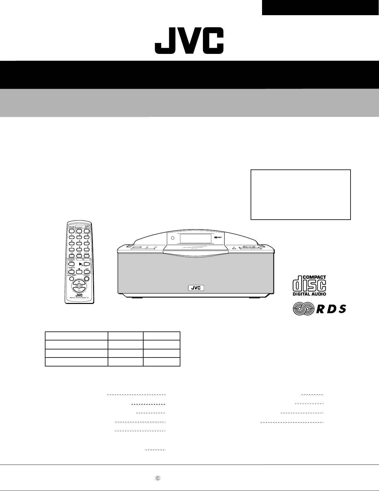
RD-T70RBU/RD-T50RLB
SERVICE MANUAL
CD PORTABLE SYSTEM
RD-T70RBU
RD-T50RLB
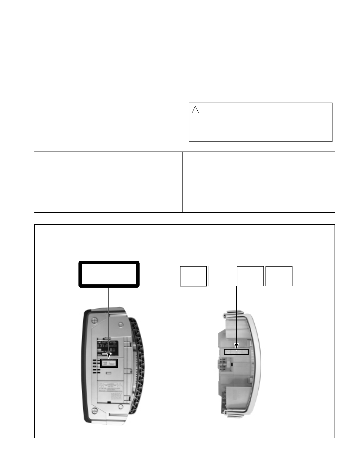
Area suffix
[RD-T70RBU Only]
Comparison table
Item RD-T50RLB RD-T70RBU
AHB Not used Used
Back light (LCD) Not used Used
Remorte control Not used Used
B ------------------------------- U.K.
E ----------- Continental Europe
EN ------------ Northern Europe
EV -------------- Eastern Europe
Contents
Safety precautions
Preventing static electricity
Important for laser products
Disassembly method
Adjustment method
Flow of functional operation
until TOC read
COPYRIGHT 2002 VICTOR COMPANY OF JAPAN, LTD.
1-2
1-4
1-5
1-6
1-13
1-15
Maintenance of laser pickup
Replacement of laser pickup
Description of major ICs
Wiring connection
1-16
1-16
1-17
1-26
No.21107
Jul. 2002
Page 2
RD-T70RBU/RD-T50RLB
1. This design of this product contains special hardware and many circuits and components specially for safety
purposes. For continued protection, no changes should be made to the original design unless authorized in
writing by the manufacturer. Replacement parts must be identical to those used in the original circuits. Services
should be performed by qualified personnel only.
2. Alterations of the design or circuitry of the product should not be made. Any design alterations of the product
should not be made. Any design alterations or additions will void the manufacturer`s warranty and will further
relieve the manufacture of responsibility for personal injury or property damage resulting therefrom.
3. Many electrical and mechanical parts in the products have special safety-related characteristics. These
characteristics are often not evident from visual inspection nor can the protection afforded by them necessarily
be obtained by using replacement components rated for higher voltage, wattage, etc. Replacement parts which
have these special safety characteristics are identified in the Parts List of Service Manual. Electrical
components having such features are identified by shading on the schematics and by ( ) on the Parts List in
the Service Manual. The use of a substitute replacement which does not have the same safety characteristics
as the recommended replacement parts shown in the Parts List of Service Manual may create shock, fire, or
other hazards.
4. The leads in the products are routed and dressed with ties, clamps, tubings, barriers and the like to be
separated from live parts, high temperature parts, moving parts and/or sharp edges for the prevention of
electric shock and fire hazard. When service is required, the original lead routing and dress should be
observed, and it should be confirmed that they have been returned to normal, after re-assembling.
5. Leakage currnet check (Electrical shock hazard testing)
After re-assembling the product, always perform an isolation check on the exposed metal parts of the product
(antenna terminals, knobs, metal cabinet, screw heads, headphone jack, control shafts, etc.) to be sure the
product is safe to operate without danger of electrical shock.
Do not use a line isolation transformer during this check.
Plug the AC line cord directly into the AC outlet. Using a "Leakage Current Tester", measure the leakage
current from each exposed metal parts of the cabinet, particularly any exposed metal part having a return
path to the chassis, to a known good earth ground. Any leakage current must not exceed 0.5mA AC (r.m.s.).
Alternate check method
Plug the AC line cord directly into the AC outlet. Use an AC voltmeter having, 1,000 ohms per volt or more
sensitivity in the following manner. Connect a 1,500 10W resistor paralleled by a 0.15 F AC-type capacitor
between an exposed metal part and a known good earth ground.
Measure the AC voltage across the resistor with the AC
voltmeter.
Move the resistor connection to each exposed metal part,
particularly any exposed metal part having a return path to
the chassis, and meausre the AC voltage across the resistor.
Now, reverse the plug in the AC outlet and repeat each
measurement. Voltage measured any must not exceed 0.75 V
AC (r.m.s.). This corresponds to 0.5 mA AC (r.m.s.).
0.15 F AC TYPE
1500 10W
Good earth ground
AC VOLTMETER
(Having 1000
ohms/volts,
or more sensitivity)
Place this
probe on
each exposed
metal part.
!
1. This equipment has been designed and manufactured to meet international safety standards.
2. It is the legal responsibility of the repairer to ensure that these safety standards are maintained.
3. Repairs must be made in accordance with the relevant safety standards.
4. It is essential that safety critical components are replaced by approved parts.
5. If mains voltage selector is provided, check setting for local voltage.
Burrs formed during molding may
be left over on some parts of the
chassis. Therefore, pay attention to
such burrs in the case of
preforming repair of this system.
In regard with component parts appearing on the silk-screen printed side (parts side) of the PWB diagrams, the
parts that are printed over with black such as the resistor ( ), diode ( ) and ICP ( ) or identified by the " "
mark nearby are critical for safety.
(This regulation does not correspond to J and C version.)
1-2
Page 3
RD-T70RBU/RD-T50RLB
(U.K only)
1. This design of this product contains special hardware and many circuits and components specially
for safety purposes. For continued protection, no changes should be made to the original
design unless authorized in writing by the manufacturer. Replacement parts must be identical to
those used in the original circuits.
2. Any unauthorised design alterations or additions will void the manufacturer's guarantee ; furthermore the
manufacturer cannot accept responsibility for personal injury or property damage resulting therefrom.
3. Essential safety critical components are identified by ( ) on the Parts List and by shading on the
schematics, and must never be replaced by parts other than those listed in the manual. Please note
however that many electrical and mechanical parts in the product have special safety related
characteristics. These characteristics are often not evident from visual inspection. Parts other than
specified by the manufacturer may not have the same safety characteristics as the recommended
replacement parts shown in the Parts List of the Service Manual and may create shock, fire, or
other hazards.
4. The leads in the products are routed and dressed with ties, clamps, tubings, barriers and the
like to be separated from live parts, high temperature parts, moving parts and/or sharp edges
for the prevention of electric shock and fire hazard. When service is required, the original lead
routing and dress should be observed, and it should be confirmed that they have been returned
to normal, after re-assembling.
1. Service should be performed by qualified personnel only.
2. This equipment has been designed and manufactured to meet international safety standards.
3. It is the legal responsibility of the repairer to ensure that these safety standards are maintained.
4. Repairs must be made in accordance with the relevant safety standards.
5. It is essential that safety critical components are replaced by approved parts.
6. If mains voltage selector is provided, check setting for local voltage.
!
Burrs formed during molding may be left over on some parts of the chassis. Therefore,
pay attention to such burrs in the case of preforming repair of this system.
1-3
Page 4
RD-T70RBU/RD-T50RLB
Preventing static electricity
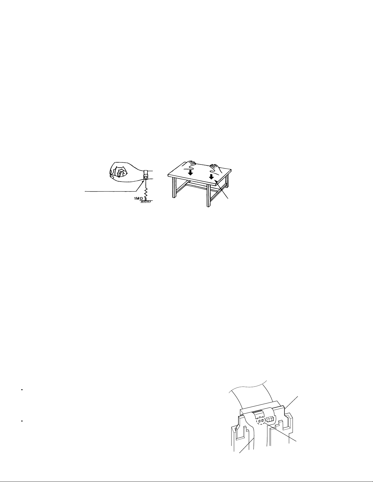
1. Grounding to prevent damage by static electricity
Electrostatic discharge (ESD), which occurs when static electricity stored in the body, fabric, etc. is discharged,
can destroy the laser diode in the traverse unit (optical pickup). Take care to prevent this when performing repairs.
2. About the earth processing for the destruction prevention by static electricity
Static electricity in the work area can destroy the optical pickup (laser diode) in devices such as CD players.
Be careful to use proper grounding in the area where repairs are being performed.
2-1 Ground the workbench
Ground the workbench by laying conductive material (such as a conductive sheet) or an iron plate over it
before placing the traverse unit (optical pickup) on it.
2-2 Ground yourself
Use an anti-static wrist strap to release any static electricity built up in your body.
(caption)
Anti-static wrist strap
Conductive material
(conductive sheet) or iron plate
3. Handling the optical pickup
1.
In order to maintain quality during transport and before installation, both sides of the laser diode on the
replacement optical pickup are shorted. After replacement, return the shorted parts to their original condition.
(Refer to the text.)
2.
Do not use a tester to check the condition of the laser diode in the optical pickup. The tester's internal power
source can easily destroy the laser diode.
4. Handling the traverse unit (optical pickup)
1.
Do not subject the traverse unit (optical pickup) to strong shocks, as it is a sensitive, complex unit.
2.
Remove solder of the short land on the flexible wire after replacing the optical pickup. For specific details, refer
to the replacement procedure in the text. Remove the anti-static pin when replacing the traverse unit.
Be careful not to take too long a time when attaching it to the connector.
3.
Handle the flexible wire carefully as it may break when subjected to strong force.
4.
It is not possible to adjust the semi-fixed resistor that adjusts the laser power. Do not turn it.
5. Attention when traverse unit is decomposed
*Please refer to "Disassembly method" in the text for the CD pickup unit.
Apply solder to the short land before the flexible wire is disconnected
from the connector on the CD pickup unit.
(If the flexible wire is disconnected without applying solder, the CD
pickup may be destroyed by static electricity.)
In the assembly, be sure to remove solder from the short land after
connecting the flexible wire.
1-4
CD pickup unit
Short land
Flexible wire
Page 5
Important for laser products
RD-T70RBU/RD-T50RLB
1.CLASS 1 LASER PRODUCT
2.DANGER : Invisible laser radiation when open and inter
lock failed or defeated. Avoid direct exposure to beam.
3.CAUTION : There are no serviceable parts inside the
Laser Unit. Do not disassemble the Laser Unit. Replace
the complete Laser Unit if it malfunctions.
4.CAUTION : The compact disc player uses invisible
laserradiation and is equipped with safety switches
whichprevent emission of radiation when the drawer is
open and the safety interlocks have failed or are de
feated. It is dangerous to defeat the safety switches.
VARNING : Osynlig laserstrålning när denna del är öppnad
och spårren är urkopplad. Betrakta ej strålen.
VARO : Avattaessa ja suojalukitus ohitettaessa olet
alttiina näkymättömälle lasersäteilylle.Älä katso
säteeseen.
5.CAUTION : If safety switches malfunction, the laser is able
to function.
6.CAUTION : Use of controls, adjustments or performance of
procedures other than those specified herein may result in
hazardous radiation exposure.
CAUTION
!
Please use enough caution not to
see the beam directly or touch it
in case of an adjustment or operation
check.
ADVARSEL : Usynlig laserstråling ved åbning , når
sikkerhedsafbrydere er ude af funktion.
Undgåudsættelse for stråling.
ADVARSEL : Usynlig laserstråling ved åpning,når
sikkerhetsbryteren er avslott. unngå utsettelse
for stråling.
REPRODUCTION AND POSITION OF LABELS
CLASS 1
LASER PRODUCT
DANGER: Invisible laser
radiation when open and
interlock failed or defeated.
AVOID DIRECT EXPOSURE
TO BEAM. (e)
WARNING LABEL
ADVARSEL: Usynlig laser-
stråling ved åbning, når
sikkerhedsafbrydere er ude
af funktion. Undgåudsæt-
telse for stråling. (d)
VARNING: Osynlig laserstrålning när denna del
är öppnad och spärren är
urkopplad. Betrakta ej
strålen. (s)
Avattaessa ja suo-
VARO:
jalukitus ohitettaessa
alttiina näkymättö
lasersäteilylle.
säteeseen. (f)
olet
mälle
Älä katso
1-5
Page 6
RD-T70RBU/RD-T50RLB
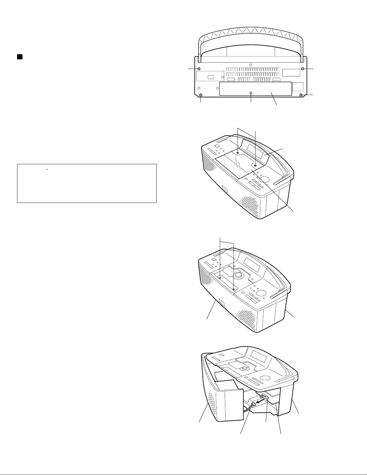
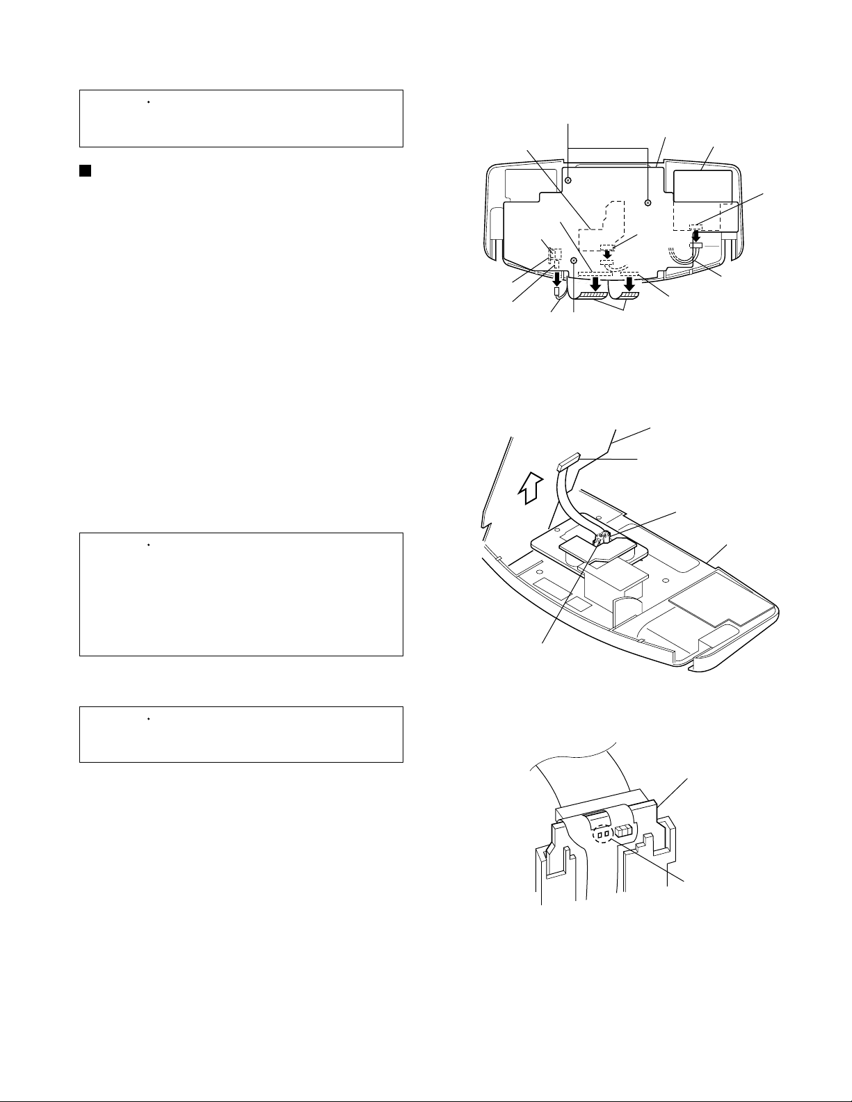
Disassembly method
<Main body section>
Removing the front cabinet assembly
and rear cabinet assembly
(See Figs.1 to 4)
1.
Remove the two screws A and two screws B
retaining the front cabinet and rear cabinet
assemblies from the rear of the body.
2.
Remove the battery door from the rear of the body,
then remove the screw C retaining the front cabinet
and rear cabinet assemblies.
3.
Remove the two screws D retaining the CD door
lens from the top of the body with a hexagonal
wrench.
[Caution] If the CD door cannot be opened, the
screws E which are to be removed in
step 4 will not be removable. In this
case, it is necessary to remove the
CD door lens.
A
B
C
Fig.1
D
A
B
Battery door
LCD lens
4.5.Remove the two screws E retaining the front
cabinet assembly from the top of the body.
Disconnect the wire from the connector CN301 on
the main board, then remove the front cabinet
assembly from the rear cabinet assembly.
(See Fig.4.)
E
Front cabinet
assembly
CD door lens
Fig.2
Rear cabinet
assembly
Fig.3
1-6
Front cabinet
assembly
Speaker wire
Fig.4
CN301
Rear cabinet
assembly
Main board
Page 7
<Front cabinet section>
Prior to performing the following procedures,
remove the front cabinet assembly from the rear
cabinet assembly.
Remove the right and left speaker
assemblies (See Figs.5 and 6)
1.2.Remove the six screws F retaining the speaker net
from the inside of the front cabinet assembly.
Remove the tie band fixing the speaker wires.
[Note] When installing the speaker assemblies,
pass each speaker wire through the
notches a to d at the bottom of the front
cabinet before bundling the wire.
3. Remove the eight screws G retaining the right and
left speaker assemblies from the outside of the
front cabinet assembly.
<Rear cabinet section>
Prior to performing the following procedures,
remove the front cabinet assembly from the rear
cabinet assembly.
RD-T70RBU/RD-T50RLB
Front cabinet assembly Speaker net
F
FF
Tie band
Notch a
Notch b
Notch c
Speaker wire
Notch d
F
Fig.5
G
G
Left speaker
Front cabinet assembly
Right speaker
G
G
Removing the top cabinet assembly
(See Figs.7 to 9)
1.
Remove the screw H retaining the top cabinet
assembly from the rear of the rear cabinet
assembly.
2.
Disconnect the wires from the connectors CN302
and CN303 on the main board at the front of the
rear cabinet assembly. (See Fig.8.)
3.
Loosen the screw J clamping the FM antenna wire.
4.
Pull the top cabinet assembly slightly towards front
and separate it from the rear cabinet assembly,
then remove the FM antenna wire from the post pin
on the main board and remove the top cabinet
assembly.
[Caution] When installing the top cabinet
assembly, be sure to connect the FM
antenna wire.
FM antenna wire
CN303
CN302
Fig.6
Top cabinet assembly
H
Rear cabinet assembly
Fig.7
Top cabinet assembly
Rear cabinet
assembly
J
Main board
Fig.8
Post pin
FM antenna wire
Rear cabinet assembly
WireWire
Fig.9
Main board
1-7
Page 8
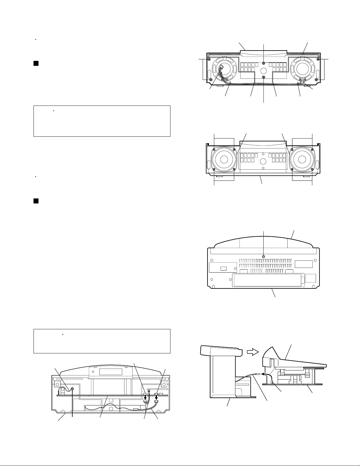
RD-T70RBU/RD-T50RLB
Removing the power supply board and
transformer assembly
Prior to performing the following procedures,
remove the top cabinet assembly from the rear
cabinet assembly.
1.
Remove the two screws K retaining the power
supply board.
2.
Remove the two screws L retaining the transformer
assembly.
3.
Pull out the power supply board from notches e
and f and remove it together with the transformer
assembly.
[Note] After assembly, apply a locking agent to
the screw L.
(See Fig.10)
Removing the battery board
(See Figs.11 and 12)
1.
Disconnect the wire from the connector CN302 on
the main board. (See Fig.11.)
2.
Remove the solder g fixing the wire.
3.
Lift the claw j on the bottom of the rear cabinet
assembly slightly and remove the battery board by
pulling it in the direction of the arrow.
Notch e
Rear cabinet assembly
Main board
Solder g
Notch h
K
Fig.10
Fig.11
Power supply board
Notch f
Transformer
assembly
L
Wire
Notch i
CN302
Wire
[Note] When installing the battery board, pass
the wires through the notches h and i at
the bottom of the rear cabinet.
Removing the handle (See Fig.13)
Prior to performing the following procedures,
remove the top cabinet assembly from the rear
cabinet assembly.
1.Open hooks k and m on the left and right sides of
the rear cabinet assembly and remove the handle
by pulling it toward the rear.
Rear cabinet assembly
Hook k
Claw j
Battery board
Fig.12
Handle
Hook m
1-8
Fig.13
Rear cabinet
assembly
Page 9
<Top cabinet section>
RD-T70RBU/RD-T50RLB
[Caution] When removing the board assembly,
be careful not to scratch or damage
the top cabinet or the CD door.
Removing the main board
(See Figs.14 to 16)
1.
Remove the three screws M retaining the main
board.
2.
Disconnect the wire and card wires from the
connectors CN708, CN801 and CN802 on the
main board. (See Fig.14.)
3.
Disconnect the wire from the connector CN804 on
the key 2 board. (See Fig.14.)
4.
Disconnect the wire from the connector CN714 on
the door switch board. (See Fig.14.)
5.
Disconnect the wire from the connector P011 on
the CD mechanism board. (See Fig.14.)
6.
Lift the main board slightly in the direction of the
arrow and apply solder to short land section n on
the CD pickup unit.
[Caution] Be sure to apply solder in order to
short land section n on the CD
pickup unit before removing the wire
from the CD pickup unit (see Fig. 16).
If the card wire is removed without
applying this solder, the CD pickup
may be damaged.
7. After soldering, disconnect the card wire from the
connector CN701 on the main board. (See Fig.15.)
CD mechanism
board assembly
Door switch
board
CN708
CN802
CN714
Wire
Short land
section n
M
M
Main board
P011
Card wires
Fig.14
CN701
Fig.15
Key 2 board
CN804
Wire
CN801
Main board
CD pickup unit
Top cabinet
[Caution] After re-connecting the card wire,
be sure to remove the solder from
short land n.
CD pickup unit
Short land
section n
Fig.16
1-9
Page 10

RD-T70RBU/RD-T50RLB
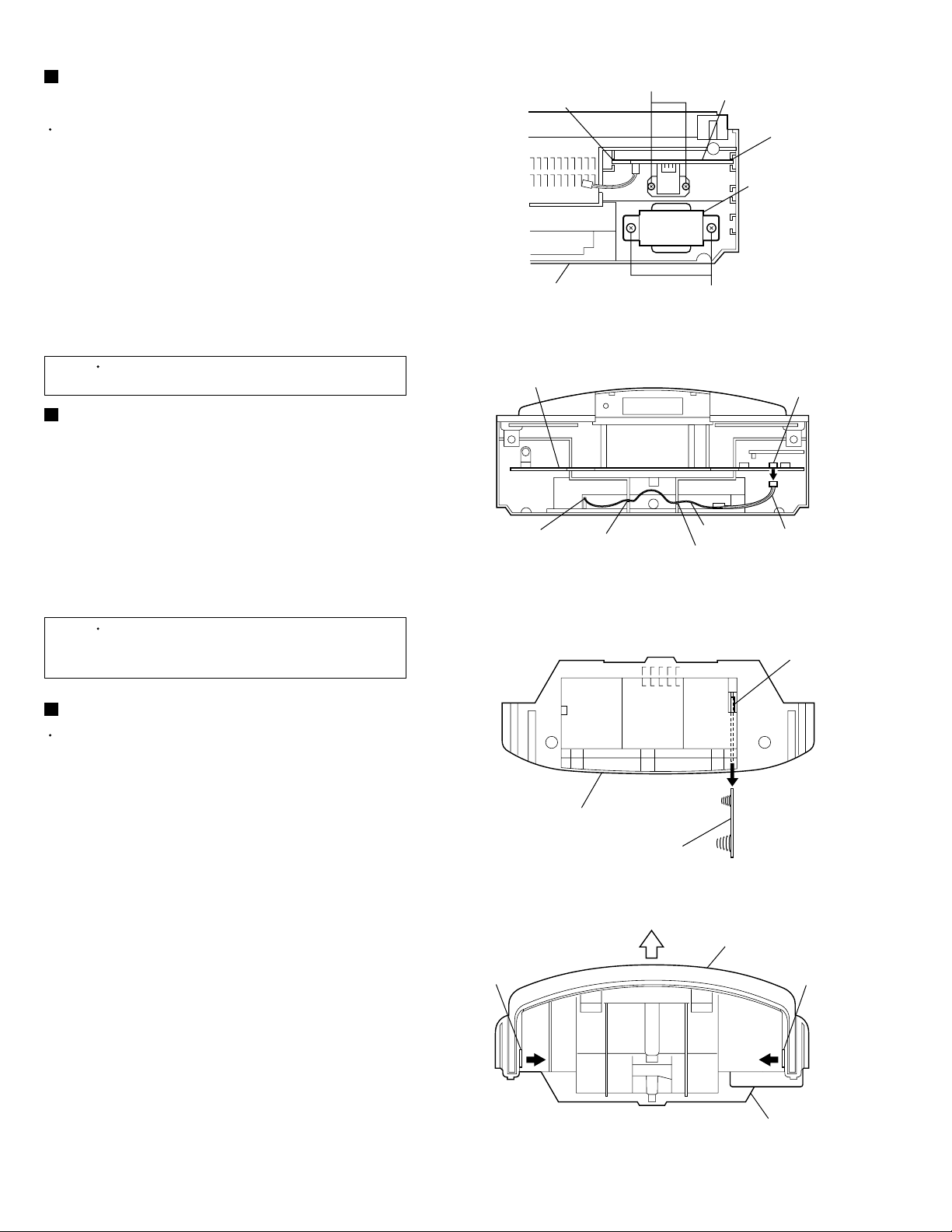
Removing the key 1 board
(See Fig.17)
1.Remove the four screws N retaining the key 1
board from the back side of the top cabinet
assembly.
Removing the key 2 board and jog
board (See Figs.18 and 19)
1.
Insert a thin tool such as the tip of a thin
screwdriver into the hole p at the back of the top
cabinet assembly and push out the jog knob toward
the front of the top cabinet assembly.
Top cabinet
N
Key 1 board
N
Fig.17
P
2.
Remove the five screws P retaining the key 2 board
from the back side of the top cabinet assembly.
3.
Remove the nut Q and washer retaining the shaft
at the top of the top cabinet assembly.
4.
Take out the key 2 board and the jog board
together.
[Note] Operation knobs are present below the
key 2 board. Be sure to install these in
their correct orientations when installing
the key 2 board. (See Fig. 20.)
In the assembly, apply a locking agent to
the nut Q.
Top cabinet
Operation knob
(RD-T70 only)
Jog board
Hole p
Key 2 board
P
Fig.18
Jog knob
Shaft
Q
1-10
Operation knobs
Washer
Top cabinet
Fig.19Fig.20
Page 11

RD-T70RBU/RD-T50RLB
Removing the CD mechanism
assembly (See Fig.21)
Prior to performing the following procedures,
remove the main board.
1.Remove the four screws R retaining the CD
mechanism assembly.
[Caution] When replacing the CD mechanism
assembly, be sure not to mistake the
positions of the red and green
dampers. (See Fig.22)
Green
Removing the door switch board
(See Fig.21)
Prior to performing the following procedures,
remove the main board.
1.Remove the screw S retaining the door switch
board.
Top cabinet
R
CD mechanism assembly
Fig.21
S
Door switch
board
R
Red
Replacing the loading belt and CD
door motor (See Figs.23 and 24)
Prior to performing the following procedures,
remove the main board.
1.
Remove the loading belt from the pulley of the CD
door motor.
2.
Remove the wire from the CD door motor by
accessing it through notch q on the CD door motor
holder.
3.
Remove the three screws T retaining the CD door
motor holder.
4.
Remove the CD door motor.
Green
Pulley
Loading belt
T
Red
Fig.22
Wire
Notch q
T
Fig.23
CD door motor
Fig.24
1-11
Page 12

RD-T70RBU/RD-T50RLB
Removing the FL display board
(See Figs.25 to 27)
Prior to performing the following procedures,
remove the main board.
1.
While keeping the sections r and s on the left and
right sides of the top cabinet assembly in the
direction of the arrow, remove the CD door from the
top cabinet.
2.
Remove the two screws W retaining the CD door
cover.
3.
Remove the two screws X retaining the FL display
board.
[Note] Before attaching the CD door cover,
pass the card wires of the FL display
board through the holes t and u on the
CD door cover. (See Fig.26.)
W
Section r
Hole t
CD door
Fig.25
Section s
Top cabinet
Card wires
Hole u
W
<CD mechanism section>
Removing the CD pickup unit
(See Figs.28 and 29)
Prior to performing the following procedures,
remove the CD mechanism assembly.
1.
Remove the four screws Y retaining the CD cover
plate.
2.
Widen the section v.
3.
While keeping the section v wide open, push the
section w in the direction of the arrow to remove
the shaft, and then remove the CD pickup.
Y
CD cover plate
CD door
X
CD door cover
Fig.26
X
FL display board
Fig.27
CD pickup unit
1-12
Y
v
Shaft
Fig.28 Fig.29
w
Page 13

Adjustment method
RD-T70RBU/RD-T50RLB
Measurement instruments required
for adjustment
1. Low frequency oscillator,
This oscillator should have a capacity to output 0dB
to 600ohm at an oscillation frequency of 50Hz-20kHz.
2. Signal generator
3. Electronic voltmeter
Measurement conditions
Power supply voltage
AC230V (50Hz)
Radio input signal
AM modulation frequency : 400Hz
Modulation factor : 30%
FM modulation frequency : 400Hz
Frequency displacement : 22.5kHz
Frequency Range
FM 87.5MHz~108MHz
65MHz~74MHz(EE version only)
MW 522kHz~1629kHz
Precautions for measurement
1. Apply 30pF and 33kohm to the IF sweeper output
side and 0.082 F and 100kohm in series to
the sweeper input side.
2. The IF sweeper output level should be made as
low as possible within the adjustable range.
3. Since the IF sweeper is a fixed device, there is
no need to adjust this sweeper.
4. Since a ceramic oscillator is used, there is no need
to perform any MPX adjustment.
5. Since a fixed coil is used, there is no need to adjust
the FM tracking.
6. The input and output earth systems are separated.
In case of simultaneously measuring the voltage
in both of the input and output systems with an
electronic voltmeter for two channels, therefore,
the earth should be connected particularly.
7. In the case of BTL connection amplifier, the minus
terminal of speaker is not for earthing. Therefore,
be sure not to connect any other earth terminal
to this terminal. This system is of an OTL system.
Standard measurement positions of volume
and switch
Power : Standby (Light STANDBY Indicator)
AHB (Active Hyper Bass) : OFF [RD-T70R only]
Main VOL. : 0 Minimum
1-13
Page 14

RD-T70RBU/RD-T50RLB
Arrangement of adjusting positions
Main board
Tuner section
Items
MW VT adjustment
(Maximum frequency)
MW VT adjustment
(Minimum frequency)
MW IFT adjustment
MW tracking
adjustment
FM VT adjustment
(Maximum frequency)
FM VT adjustment
(Minimum frequency)
FM tracking
adjustment
Note: 1. For adjusting, be sure to use a ceramic type driver.
2. The adjustment of CD section is not required.
Measurement
conditions
Input signal
MW:1629kHz
Measurement point
: VT test point
Input signal
MW:522kHz
Measurement point
: VT test point
Input signal
: 1404kHz
Input signal
: 621kHz
Input signal
: 1404kHz
Input signal
: 621kHz/1404kHz
Input signal
:108MHz
Measurement point
: VT test point
Input signal
MW:87.5MHz
Measurement point
: VT test point
Input signal
:98MHz
1. Set the MW signal generator signal to 1629kHz and feed
it to Loop Antenna.
2. Receiving the signal and adjust the MW OSC coil
L16 obtain the VT is 4.4V +/- 0.1V.
3. Set the MW signal generator signal to 522kHz and feed it
to Loop Antenna.
4. Receiving the signal and confirm that VT is 1.2V+/-0.2V.
5. Change the receiving frequency to 1404kHz.
6. Adjust the MW IFT T2 obtain to maximum output.
7. Change the receiving frequency to 621kHz.
8. Adjust the antenna coil L17 obtain to maximum output.
9. Change the receiving frequency to 1404kHz.
10. Adjust the CT1 obtain to maximum output.
11. Repeat the above steps 7 to 10 of 621kHz and
1404kHz.
1. Set the FM signal generator signal to 108MHz and
receive the 108MHz.
2. Receiving the signal and adjust the FM OSC coil L11
obtain the VT is 4.0+/-0.1V.
3. Set the FM signal generator signal to 87.5MHz and
receive the 87.5MHz.
4. Receiving the signal and confirm that VT is 1.75V+/-0.2V.
5. Change the receiving frequency to 98MHz.
6. Adjust the FM RF coil L14 obtain the maximum output.
Measurement method
Standard
values
V.T : 4.4V+/-0.1V
V.T : 1.2V+/-0.2V
Maximum output
Maximum output
Maximum output
VT: 4.0+/-0.1V
VT:1.75+/-0.2V
Maximum output
Adjusting
positions
MW OSC coil: L16
Adjust the OSC coil
only when the MW
coil block has been
changed.
MW IFT: T2
Adjust the IFT only
when the IFT block
has been changed.
Antenna coil: L17
CT1
FM OSC coil: L11
FM RF coil: L14
1-14
Page 15

Flow of functional operation until TOC read
Power ON
Play Key
Slider turns REST
SW ON.
Automatic tuning
of TE offset
Confirm that the voltage at the pin5
of CN705-1 is "H"\"L"\"H".
RD-T70RBU/RD-T50RLB
Check Point
Tracking error waveform at TOC reading
Approx.3sec
Tracking
servo
off states
Automatic measurement
of TE amplitude and
automatic tuning of
TE balance
VREF
pin 20 of
IC702(TE)
Approx.
1.8V
Disc states
to rotate
Tracking
servo
on states
Disc to be
braked to stop
TOC reading
finishes
500mv/div
2ms/div
Fig.1
Laser ON
Detection of disc
Automatic tuning of
Focus offset
Automatic measurement of
Focus S-curve amplitude
Disc is rotated
Focus servo ON
(Tracking servo ON)
Automatic measurement of
Tracking error amplitude
Automatic tuning of
Tracking error balance
Check that the voltage at the
pin40 of IC701 is + 5V?
Confirm that the Focus error
S-cuve signal at the pin32 of
IC701 is approx.2Vp-p
Confirm that the signal from
pin24 IC701 is 0V as a
accelerated pulse during
approx.400ms.
Confirm the waveform of
the Tracking error signal.
at the pin 20 of IC702 (R705)
(See Fig.1)
Automatic tuning of
Focus error balance
Automatic tuning of
Focus error gain
Automatic tuning of
Tracking error gain
TOC reading
Play a disc
Confirm the eye-pattern
at the lead of TP713
1-15
Page 16

RD-T70RBU/RD-T50RLB
Maintenance of laser pickup
(1) Cleaning the pick up lens
Before you replace the pick up, please try to
clean the lens with a alcohol soaked cotton
swab.
(2) Life of the laser diode
When the life of the laser diode has expired,
the following symptoms will appear.
1. The level of RF output (EFM output:ampli tude of eye pattern) will below.
Is the level of
RFOUT under
1.25V 0.22Vp-p?
YES
O.K
NO
Replace it.
Replacement of laser pickup
Turn off the power switch and,disconnect the
power cord from the AC OUTLET.
Replace the pickup with a normal one.(Refer
to "Pickup Removal" on the previous page)
Plug the power cord in,and turn the power on.
At this time,check that the laser emits for
about 3seconds and the objective lens moves
up and down.
Note: Do not observe the laser beam directly.
Play a disc.
Check the eye-pattern at TP713.
Finish.
(3) Semi-fixed resistor on the APC PC board
The semi-fixed resistor on the APC printed circuit board which is
attached to the pickup is used to adjust the laser power.Since this adjustment should be performed to match the
characteristics of the whole optical block, do not touch the semi-fixed resistor.
If the laser power is lower than the specified value,the laser diode is almost worn out, and the laser pickup should
be replaced.
If the semi-fixed resistor would be adjusted when the pickup operates normally,the laser pickup may be damaged
due to excessive current.
1-16
Page 17

Description of major ICs
AN22000A (IC702) : RF & Servo amplifier
1. Terminal layout 2. Block diagram
3TOUT
CEA
9 10 15 22 23 21 20 19 18 2 1
14
OFTR 3TENV
13
12
BDO
11
8
AGC
7
6
5
4
NRFDET
RF_EQ
10
11
12
13
14
15
16
1
2
3
4
5
6
7
8
9
32
31
30
29
28
27
26
25
24
23
22
21
20
19
18
17
OFTR
COFTR
BDO
CBOO
ARF
CAGC
RFIN
RFOUT
RFN
FEN
FEOUTNRFDET
SUBT SUBT
BCA
GCA
TEN
BCA
GCA
BCA
GCA
AMPAMPAMP
RD-T70RBU/RD-T50RLB
VDET
TEBPFTEOUT
VDET
BCA
GCA
AMP
PDLD
3
VCC
16
GND
FBAL
25
26
TBAL
GCTL
24
3. Pin function
A C B D E F VREF
Pin No. Symbol Function
1
2
3
4
5
6
7
8
9
10
11
12
13
14
15
16
17
18
19
20
21
22
23
24
25
26
27
28
29
30
31
32
PD
LD
VCC
RFN
RFOUT
RFIN
CAGC
ARF
CEA
3TOUT
CBOO
BDO
COFTR
OFTR
NRFDET
GND
VREF
VDET
TEBPF
TEOUT
TEN
FEN
FEOUT
GCTL
FBAL
TBAL
E
F
D
B
C
A
APC Amp. Input terminal
APC Amp.Output terminal
Power supply terminal
RF addition Amp.Reversing input terminal
RF addition Amp.Output terminal
AGC input terminal
Terminal of connection of capacity of AGC loop filter.
AGC output terminal
Capacity connection terminal for HPF-Amp.
3TENV output terminal
Capacity connection terminal for RF shade side envelope detection
BDO output terminal
Capacity connection terminal for RF discernment side envelope detection
OFTR output terminal
RFDET output terminal (Negative logic)
Earth terminal
VREF output terminal (Not use)
VDET output terminal (Not use)
VDET input terminal
TE Amp. output terminal
TE Amp. reversing input terminal
FE Amp. reversing input terminal
FE Amp. output terminal
Terminal GCTL & APC
FBAL control terminal
TBAL control terminal
Tracking signal input terminal 1
Tracking signal input terminal 2
Focus signal input terminal 4
Focus signal input terminal 2
Focus signal input terminal 3
Focus signal input terminal 1
2729303132
28
17
1-17
Page 18

RD-T70RBU/RD-T50RLB
MN101C38CYE (IC801) : System controller
1.Terminal layout
100 76
1
25
26 50
2. Pin function
Pin No.
1~4
5~7
8
9
10
11
12
13
14
15
16~18
19
20, 21
22
23
24
25
26
27
28
29
30
31
32
33
34
35
36
37
38
39
40
41
42
43
44~46
47
48
49
50
75
51
Symbol Function
COM 4~1
VLC 3~1
VDD
OSC2
OSC1
VSS
XI
XO
MMOD
VREFKEY1~3
SFTY
VOL1, 2
ACCHK
PCHK
VREF+
VDAT
SDI
VCK
VCE
SUBQ
SQCK
SHIFT
NRST
PCNT
FTU
FCD
AHB
SMUTE
REM
BLKCK
RDDI
INH
RDCK
AL2
BUZ1~3
POWER
RESERVE2
REST
MDAT
I/O
O
LCD common outputs
-
LCD power supply
-
Power supply
O
Clock output (8MHz)
I
Clock input (8MHz)
-
Ground
I
Sub clock input (32.768kHz)
O
Sub clock output (32.768kHz)
I
Memory mode switch input
-
-Power supply for A/D converter
I
Control key signal input
I
Safety check for power off
I
Rotary digital encoder input
I
AC operate
I
Power supply check
I
+Power supply for A/D converter
O
Common data, PLL & volume
I
PLL data input
O
Common CLK, PLL & volume
O
Common CE, PLL & volume
I
CD sub code data input
O
CD sub code clock output
O
8MHz clock shift for FM receiving
I
Reset input
O
Power ON/OFF control
O
Radio VDD switching control
O
CD 5V control
O
Active bass (RD-T70 only)
O
Signal muting by muting circuit
I
Remote control signal input
I
CD sub code block clock 75Hz input
I
RDS data from decoder IC (JC version: Not use)
I
Inhibit input
I
RDS clock from decoder IC (JC version: Not use)
O
Alarm 2 output
O
Buzzer signal
I
Power key input
-
Not use
I
Pickup rest position input
O
CD common data output
1-18
Page 19

RD-T70RBU/RD-T50RLB
Pin No.
51
52
53
54
55
56
57
58
59
60
61
62
63
64
65
66
67~100
Symbol FunctionI/O
MLD
MCLK
RESERVE3
GVP
MOMU
XRST
S TAT
LED1
MPX
OSW
CSW
LOAD
OCTL
CCTL
SCTL
BLIGHT
SEG34~1
O
CD data latch output
O
CD common clock output
-
Not use
-
Not use
O
Motor driver mute control
O
CD reset output
I
Status signal input
O
Power/standby LED
I
Stereo indicator I/P
I
Door open contact switch
I
Door close contact switch
I
Door is locked signal
O
Door open control
O
Door close control
O
Door speed down
O
Backlight LED
O
LCD segment output
TA8227P (IC302) : Power amplifier
2. Block diagram1. Terminal layout
OUT1
16
12 7
B.S.1
3
2
PW GND
FIN
OUT2 B.S.2
10
11
VCC1
12
ch-1
VCC2
1
6
IN1 NF1
BA15218 (IC401) : Dual operational amplifier
1. Terminal layout & Block diagram
OUT1 1
-IN1 2
1
+IN1 3
G 4
8 Vcc
7 OUT2
6 -IN2
2
5 +IN2
BIAS CIRCUIT
30
THERMAL
SHUT DOWN
PROTECTION
CIRCUIT
45
5
9
RIPPLE
ch-2
7
8
IN2 NF2
45
30
4
PRE GND
1-19
Page 20

RD-T70RBU/RD-T50RLB
MN662748RPMFA (IC701) : Digital servo & Digital signal processor
1. Terminal layout
80 61
1
60
20
21 40
41
2. Pin function
Pin No. Symbol I/O Function
1
2
3
4
5
6
7
8
9
10
11
12
13
14
15
16
17
18
19
20
21
22
23
24
25
26
27
28
29
30
31
32
33
34
35
36
37
38
39
40
BCLK
LRCK
SRDATA
DVDD1
DVSS1
TX
MCLK
M DATA
MLD
SENSE
FLOCK
TLOCK
BLKCK
SQCK
SUBQ
DMUTE
S TAT
RST
SMCK
PMCK
TRV
TVD
PC
ECM
ECS
KICK
TRD
FOD
VREF
FBAL
TBAL
FE
TE
RFENV
VDET
OFT
TRCRS
/RFDET
BDO
LDON
-
Not use
-
Not use
-
Not use
-
Power supply for digital circuit
-
Ground for digital circuit
-
Not use
I
Micro computer command clock signal input
I
Micro computer command data input
I
Micro computer command load signal input (L: Load)
-
Not use, connect to TP716
-
Not use, connect to TP717
-
Not use, connect to TP718
O
Sub code block clock signal output
I
External clock input for sub code Q register input
O
Sub code Q data output
I
Not use, connect to TP719
O
Status signal input
I
Reset signal input (L: Reset)
-
Not use
-
Not use, connect to TP720
O
Traverse enforced output
O
Traverse drive output
-
Not used
O
Spindle motor drive signal (Enforced mode output)
O
Spindle motor drive signal (Servo error signal output)
O
Kick pulse output
O
Tracking drive output
O
Focus drive output
I
Reference voltage for D/A output block
O
Focus balance adjust signal output
O
Tracking balance adjust signal output
I
Focus error signal input (Analog input)
I
Tracking error signal input (Analog input)
I
RF envelope signal input (Analog input)
I
Vibration detect signal input (H:Detect)
I
Off track signal input (H:Off track)
I
Track cross signal input
I
RF detect signal input (L:Detect)
I
Drop out signal input (H:Drop out)
O
Laser on signal output (H:ON)
1-20
Page 21

Pin No. Symbol I/O Function
41
PLLF2
42
TOFS
43
WVEL
44
ARF
45
IREF
46
DRF
47
DSLF
48
PLLF
49
VCOF
50
AVDD2
51
AVSS2
52
EFM
53
PCK
54
VCOF2
55
SUBC
56
SBCK
57
VSS
58
X1
59
X2
60
VDD
61
BYTCK/TRVSTP
62
CLDCK
63
FCLK
64
IPFLAG
65
FLAG
66
CLVS
67
CRC
68
DEMPH
69
RESY
70
IOSEL
71
/TEST
72
AVDD1
73
OUTL
74
AVSS1
75
OUTR
76
RSEL
77
CSEL
78
PSEL
79
MSEL
80
SSEL
-
Not use
-
Not use
-
Not use
I
RF signal input
I
Reference current input
I
Bias pin for DSL
I/O
Loop filter pin for DSL
I/O
Loop filter pin for PLL
I/O
Loop filter pin for VCO
-
Power supply for analog circuit
-
Ground for analog circuit
-
Not use, connect to TP724
O
Clock output for PLL
I/O
Loop filter pin for Digital servo VCO
-
Not use
-
Not use
-
GND for crystal oscillation circuit
I
Input for crystal oscillation circuit (f=16.9344MHz)
O
Output for crystal oscillation circuit (f=16.9344MHz)
-
Power supply for crystal oscillation circuit
-
Not use
O
Sub code frame clock signal output
-
Not used
O
Interpolation flag signal output, Connect to TP721
O
Flag signal output, connect to TP722
-
Not use
-
Not use
O
De-emphasis detect signal output, Connect to TP723
-
Not use
I
Mode select pin, Connect to DVDD1 (H fix)
I
Test pin, Connect to DVDD1 (H fix)
-
Power supply for analog circuit
O
L-channel audio output
-
Ground for analog circuit
O
R-channel audio output
I
RF signal polarity setting pin, connect to DVDD1 (H fix)
I
Oscillation frequency setting pin, Connect to GND (L fix)
I
IOSEL=H, Test pin, connect to GND (L fix)
I
IOSEL=H, SMCK output, frequency select pin
I
IOSEL=H, SMCK output, SUBQ output mode select pin
RD-T70RBU/RD-T50RLB
NJM2930L05 (IC802) : Regulator
1. Terminal layout
1
123
(Bottom view)
23
1.Output
2.GND
3.InputPUT
1-21
Page 22

RD-T70RBU/RD-T50RLB
BA6897FP (IC703) : 4channel driver
1.Terminal layout & Block diagram
GND
OUT4+
OUT4-
IN4/R
28
27
26
25
IN4
24
VREF
23
VCC
22
VCC
21
IN3
20
IN3/R
19
OUT3-
18
OUT3+
17
OP-IN+
16
OP-IN-
15
Level
shift
Level
shift
D.BUF
3
IN1/R
D.BUF
4
IN1
T.S.D
5
TR-B
6
7
MUTE
REG-OUT
DRIVER
MUTE
8
GND
9
IN2
Level
Level
10
IN2/R
D.BUF
1
OUT1+
D.BUF
2
OUT1-
BU1923 (IC6) : RDS decoder
1. Terminal layout 2. Block diagram
1
QUAL
RDATA
VREF
MUX
VDD1
VSS1
VSS3
CMP
2
3
4
5
6
7
8
16
15
14
13
12
11
10
9
RCLK
NC
XO
XI
VDD2
VSS2
T2
T1
MUX
VREF
VDD1
4
3
5
Analog
Power supply
100k
120k
D.BUF
shift
shift
D.BUF
100k
11
OUT2-
D.BUF
D.BUF
12
13
GND
OUT2+
-
+
anti-aliasing
filter
14
OP-OUT
VSS3
8th Switched
capacitor filter
7
CMP
8
comparator
16
RCLK
VSS1
VDD2
VSS2
3. Pin function
Pin No. Symbol I/O Function
1
QUAL
O
Demodulator quality,
good data: Hi, bad data: Low
2
3
4
5
6
7
8
R DATA
VREF
MUX
VDD1
VSS1
VSS3
CMP
O
Demodulator data
-
Reference voltage, 1/2 VDD1
I
Composite signal input
-
Analog power supply
-
Analog ground
-
Analog ground
I
Comparator input, C-junction
6
12
Power supply
11
Digital
PLL
57kHz
RDS/ARI
13
14
XO T2 T1
Xl
PLL
1187.5Hz
Reference
clock
Bi-phase
decoder
Pin No. Symbol I/O Function
9,10
T1,T2
I
Test input,
open or connected to ground
11
12
13
14
15
16
VSS2
VDD2
XO
NC
RCLK
XI
-
Digital ground
-
Digital power supply
I
4.332MHz crystal oscillator input
O
4.332MHz crystal oscillator output
-
Not used
O
1187.5Hz demodulator clock
Differential
decoder
Measurement
circuit
10 9
1
QUAL
2
RDATA
1-22
Page 23

LA1823 (IC5) : 1chip AM/FM, MPX tuner system
1. Terminal layout & Block diagram
RD-T70RBU/RD-T50RLB
24
FM
RF
AM
RF
1 2 4 5 10 11 126 7 8 93
23
GND2
REG VCC1 GND1
22
AM
MIX
AM
OSC
21
VCC2
OSC
BUFFER
20
FM
OSC
FM
MIX
MUTE
IF
BUFFER
17 16
DECODER
ST SW
VCO FF FF
TRIG
STSD
2. Pin function
Pin No. Symbol I/O Function
1
AM_RFIN
2
REG.
3
AM_OSC
4
VCC_1
5
FM_MIXOUT
6
GND_1
7
IF_BUFFER
8
ST_IND
9
AM_MIXOUT
10
FM_IFIN
11
AM_IFIN
12
AGC
13
FM_DET
14
ST/MON_SW
15
AM/FM_SW
16
L_OUT
17
R_OUT
18
MPX_IN
19
DET_OUT
20
FM_OSC
21
VCC_2
22
FM_RFOUT
23
GND_2
24
FM_RFIN
I
AMRF signal input
I
AMRF signal input
-
AM local oscillation circuit
-
Power supply terminal
O
Output terminal for FM mixer
-
Ground
O
IF buffer output
O
Stereo indicator output
O
Output terminal for AM mixer
I
Input of FMIF signal
I
Input of AMIF signal
I
AGC voltage input terminal
O
FM detection signal output
I
Stereo/Monaural switching signal input
I
AM/FM switching signal input
O
Output L-channel
O
Output R-channel
I
Multiplex signal input
O
AM/FM detection output
-
FM local oscillation circuit
-
Power supply terminal
O
Output of FMRF signal
-
Ground
I
Input of FMRF signal
15
PHASE
COMP
FM
S-METERAMDET
FM
IF
14
PILOT
DET
FF
AM
IF
1319 18
FM
DET
AGC
1-23
Page 24

RD-T70RBU/RD-T50RLB
LC72136 (IC4) : PLL frequency synthesizer
1. Terminal layout
1
XTI
FM
CE
DI
CLOCK
DO
VCOSTOP
AM/FM
LW
MW
SDIN
2
3
4
5
6
7
8
9
10
11
22
21
20
19
18
17
16
15
14
13
12
XT
GND
LPFI
LPFO
PD
VCC
FMIN
AMIN
NC
IFCNT
IFIN
2. Block diagram
1
22
16
15
3
1/2
Reference
Driver
Swallow Counter
1/16,1/17 4bit
12bit
Programmable
Drivers
Phase
Detector
Charge Pump
Unlock
Detector
18
19
20
12
4
5
6
17
21
3. Pin function
C2B
I/F
Powe r
on
Reset
Data Shift Register & Latch
29
71311
Pin No. Symbol I/O Function
1
2
3
4
5
6
7
8
9
10
11
12
13
14
15
16
17
18
XTI
FM
CE
DI
CLOCK
DO
VCOSTOP
AM/FM
LW
MW
SDIN
IFIN
IFCNT
NC
AMIN
FMIN
VCC
PD
I
X'tal oscillator connect (75kHz)
O
LOW:FM mode
I
When data output/input for 4pin(input) and 6pin(output): H
I
Input for receive the serial data from controller
I
Sync signal input use
O
Data output for Controller, Output port
O
"Low": MW mode
O
Open state after the power on reset
-
Not use
I
AM MW signal input
I/O
Data input/output
I
IF counter signal input
O
IF signal output
-
Not use
I
AM Local OSC signal input
I
FM Local OSC signal input
-
Power supply(VDD=4.5-5.5V), When power ON:Reset circuit move
O
PLL charge pump output(H: Local OSC frequency Height than Reference
frequency. L: Low Agreement: Height impedance)
19
20
21
22
LPFO
LPFI
GND
XT
O
Output for active low pass filter of PLL
I
Input for active low pass filter of PLL
-
Connect to GND
I
X'tal oscillator (75KHz)
Universal
Counter
8
14
TA8409S (IC704) : Motor driver
1.Terminal Layout
1-24
123456789
VS
IN2
VCC
OUT 2
NC
GND
OUT 1
VR
IN1
2.Truth table
INPUT OUTPUT
IN1
IN2
OUT1
0
0
1
0
0
1
1
1
OUT2
MODE
STOP
H
L
L
L
H
L
CW/CCW
CCW/CW
BRAKE
Page 25

LC75342 (IC301) : E. volume
RD-T70RBU/RD-T50RLB
1. Terminal layout
1
DI
2
CE
3
VSS
4
TEST
5
LOUT
6
LBASS2
7
LBASS1
8
LTRE
9
LIN
10
LSELO
11
L4
12
L3
13
L2
14
L1
15
NC
3. Pin function
Pin No.
Symbol Function
1
2
3
4
5
6
7
8
9
10
11
12
13
14
15
16
DI
CE
VSS
TEST
LOUT
LBASS2
LBASS1
LTRE
LIN
LSELO
L4
L3
L2
L1
NC
NC
2. Block diagram
LSELO LIN LTRE LBASS1 LBASS2 LOUT
30
29
28
27
26
25
24
23
22
21
20
19
18
17
16
CL
VDD
VREF
NC
ROUT
RBASS2
RBASS1
RTRE
RIN
RSELO
R4
R3
R2
R1
NC
NC
NC
11
L4
12
L3
13
L2
L1
14
15
16
R1
17
R2
18
R3
19
20
R4
10
Serial data and clock input for IC
control
Chip enable
GND
Electric volume connection for test
Volume control and equalizer input
Connection for resistor and capacitor
that from the bass band filter
Connection for capacitor that from
the treble band filter
Volume control and equalizer input
Input selector output
Input signal connections, not use
Input signal connections
Input signal connections
Input signal connections
Not use
Not use
9 8 7 6 5
CONTROL
CIRCUIT
LOGIC
CIRCUIT
CONTROL
CIRCUIT
Pin No.
17
18
19
20
21
22
23
Symbol Function
R1
R2
R3
R4
RSELO
RIN
RTRE
LVref
CCB
INTERFACE
RVref
ROUTRBASS2RBASS1RTRERINRSELO
Input signal connections
Input signal connections
Input signal connections
Input signal connections, not use
Input selector output
Volume control and equalizer input
Connection for capacitor that from
the treble band filter
24
25
26
27
28
RBASS1
RBASS2
ROUT
VREF
Connection for resistor and capacitor
that from the bass band filter
Volume control and equalizer input
NC
Not use
Connection to the 0.5X VDD voltage
generator circuit used as the analog
signal ground
29
30
VDD
CL
Power supply
Serial data and clock input for IC
control
4
TEST
3
VSS
2
CE
1
DI
CL
30
VDD
29
VREF
28
NC
27
262524232221
SPS-445-1-E1 (IC803) : Remote control receiver
1. Terminal layout
123
1 : GND
2 : Vout
3 : Vcc
2. Block diagram
Amp. Limiter
ABLC
BPF
+
TRAP
Detector
Waveform
Shaper
V
CC
R
L
V
out
GND
1-25
Page 26

RD-T70RBU/RD-T50RLB
Wiring connection
Speaker R-ch
GJ351020192612
2
0
2
0
2
Speaker L-ch
CN302
E
BU.+
Battery board
CN802 CN801
FL display board
GJ353130080107
Headphone jack
CN801
CN802
HP301
GJ354006160110
9
0
CN804
GJ3510000072612
D
GJ351000052612
CN709
Main board
GJ354006150100
CN301
CN302
CN303
CN705
9
0
2
0
2
0
GJ354006230110
0
9
J34
J35
J36
VR801
CN804
Color codes and shown colors
2 ............................... Red
8 ............................... Grey
9 ............................... White
Jog board
CN803
1
GJ353040210200
1
CN803
0 ............................... Black
Key 2 board
Volume board
AHB board
(RD-T70R only)
D
C
C
CN701
Key 1 board
GJ354006190100
1-26
GJ353240080107
RD-T50R
GJ354006140100
2
0
CD door motor
GJ353280080107
RD-T70R
20
8
GJ3510910522031
B
CN708
A
FM ANT
SW701
CN714
B
00
GJ351000082612
GJ351000092612
GJ354006170110
Door switch
board
A
GJ354006180110
9
0
CD mechanism assembly
Spindle motor
GJ353150060207
Feed motor
CD
pickup unit
CN303
J902
2
AC INPUT
0
Power supply board
AC power cord
Page 27

< MEMO >
RD-T70RBU/RD-T50RLB
1-27
Page 28

RD-T70RBU/RD-T50RLB
VICTOR COMPANY OF JAPAN, LIMITED
AUDIO & COMMUNICATION BUSINESS DIVISION
PERSONAL & MOBILE NETWORK BUSINESS UNIT. 10-1,1Chome,Ohwatari-machi,maebashi-city,371-8543,Japan
No.21107
200207
 Loading...