

Page 1
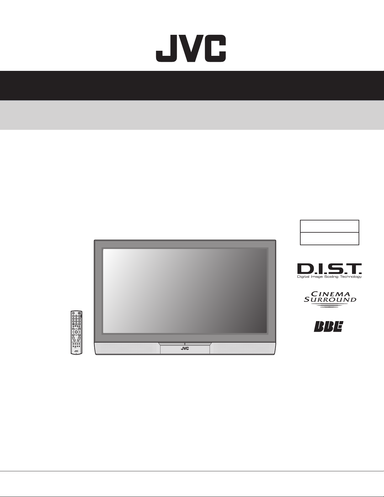
SERVICE MANUAL
PDP COLOUR TELEVISION
PD-Z35DV4, PD-Z35DV4
/S
PD-Z42DV4, PD-Z42DV4/S
BASIC C
HASSIS
FP2
1 PRECAUTION
2 SPECIFIC SERVICE INSTRUCTIONS
3 DISASSEMBLY
4 ADJUSTMENT
5 TROUBLESHOOTING
......................................................................................................................................................... 1-3
..................................................................................................................................................... 1-11
...................................................................................................................................................... 1-28
........................................................................................................................................... 1-40
COPYRIGHT © 2004 Victor Company of Japan, Limited
TABLE OF CONTENTS
...................................................................................................................... 1-6
No.YA101
2004/7
Page 2
SPECIFICATION
Contents
Items
Dimensions (W x H x D)
Mass 38.3kg 30.4kg
TV RF System CCIR B / G, I, D / K, K1, M
Colour System RF PAL / SECAM / NTSC3.58 / NTSC4.43
VIDEO PAL / SECAM / NTSC3.58 / NTSC4.43
Stereo System A2 (B / G), NICAM (B / G, I, D / K / K1)
Teletext System FLOF (Fastext), TOP, WST (World Standard System)
Receiving Frequency VHF Low 46.25MHz ~ 168.25MHz
VHF High 175.25MHz ~ 463.25MHz
Intermediate VIF 38.0MHz (B / G, I, D / K, K1, M)
Frequency SIF
Colour Sub Carrier Frequency
Power Input AC110V ~ AC240V, 50Hz / 60Hz
Power Consumption Operate : 303W, Stand by: 3.0W Operate : 244W, Stand by : 3.0W
Plasma Display Panel (PDP) QLE0028-001 QLE0021-001
Screen Size Visible size : 107.5cm (Diagonal) / Visible size : 91.0cm (Diagonal) /
Display Pixels
Speaker 6.6cm round x4, (Oblique cone)
Audio Power Output 10W + 10W
Aerial Input Teminal 75Ω unbalanced, coaxial
Video / Audio Iutput S-Video [1/2/4] Mini-DIN 4 pin connector x3
[1/2/3/4] Y : 1V(p-p), 75Ω, positive (negative sync)
Component Video [1/3]
1125i / 750p Y : 1V(p-p), 75Ω, 3-value sync : ±0.35V(p-p)
525i / 525p
Video / Audio Output Video 1V(p-p), 75Ω, RCA pin jack x1
Audio Output (Fixed) 500mV (rms), low impedance, RCA pin jack x 2
Subwoofer Output 500mV (rms), low impedance, RCA pin jack x 1
Center CH Input 500mV (rms), low impedance, RCA pin jack x 1
PC (RGB) Input D-sub 15pin x 1
Headphone 3.5mm Stereo mini jack x 1
Remote Control Unit RM-C1830H (AA/R6 TYPE battery x 2)
Design & specifications are subject to change without notice.
104.5cm x 72.9cm x 11.0cm 90.7cm x 63.4cm x 11.7cm
UHF 471.25MHz ~ 863.25MHz
CATV Mid: X ~ Z+2, S1~S10
Super: S11 ~ S20
Hyper: S21 ~ S41
33.4MHz (5.5MHz: B / G) / 32.9MHz (6.0MHz: I) / 32.4MHz (6.5MHz: D / K, K1) /
33.5MHz (4.5MHz :M)
PAL : 4.43MHz
SECAM : 4.40MHz / 4.25MHz
NTSC : 3.58MHz / 4.43MHz
42V wide aspect (16:9) 35V wide aspect (16:9)
93.3 cm x 53.3 cm (H x V) 78.6 cm x 44.2 cm (H x V)
H: 852 pixels / V: 480 pixels
C: 0.286V(p-p) (Burst signal), 75
Video 1V(p-p), 75Ω, negative sync, RCA pin jack x4
Audio 500mV(rms) (-4dBs), high impedance, RCA pin jack x8
RCA pin jack x 3
Pb/Pr : ±0.35V(p-p), 75
Y : 1V(p-p), 75Ω, positive (Negative sync)
Pb / Pr : 0.7V(p-p), 75
Audio 500mV(rms)(-4dBs), low impedance (400Hz when modulated 100%),
RCA pin jack x2
R/G/B : 0.7V (p-p), 75
HD / VD : 1V (p-p) to 5V (p-p), high impedance
<Available signal>
VGA : 640 pixels x 480 pixels (Horizontal : 31.5kHz / Vertical : 60Hz)
PD-Z42DV4 PD-Z35DV4
PD-Z42DV4/S PD-Z35DV4/S
[W-VGA]
Ω
Ω
Ω
Ω
H: 853 pixels / V: 480 pixels
[W-VGA]
1-2 (No.YA101)
Page 3
D
SECTION 1
PRECAUTION
1. 1 SAFETY PRECAUTIONS
(1) The design of this product contains special hardware,
many circuits and components specially for safety
purposes. For continued protection, no changes should
be made to the original design unless authorized in writing
by the manufacturer. Replacement parts must be identical
to those used in the original circuits. Service should be
performed by qualified personnel only.
(2) Alterations of the design or circuitry of the products should
not be made. Any design alterations or additions will void
the manufacturer's warranty and will further relieve the
manufacturer of responsibility for personal injury or
property damage resulting therefrom.
(3) Many electrical and mechanical parts in the products have
special safety-related characteristics. These
characteristics are often not evident from visual inspection
nor can the protection afforded by them necessarily be
obtained by using replacement components rated for
higher voltage, wattage, etc. Replacement parts which
have these special safety characteristics are identified in
the parts list of Service manual. Electrical components
having such features are identified by shading on the
schematics and by () on the parts list in Service
manual. The use of a substitute replacement which does
not have the same safety characteristics as the
recommended replacement part shown in the parts list
of Service manual may cause shock, fire, or other hazards.
(4) Don't short between the LIVE side ground and ISOLATED
(NEUTRAL) side ground or EARTH side ground when
repairing.
Some model's power circuit is partly different in the GND.
The difference of the GND is shown by the LIVE : (
GND, the ISOLATED (NEUTRAL) : (
EARTH : (
) side GND. Don't short between the LIVE
) side GND and
side GND and ISOLATED (NEUTRAL) side GND or EARTH
side GND and never measure the LIVE side GND and
ISOLATED (NEUTRAL) side GND or EARTH side GND at
the same time with a measuring apparatus (oscilloscope
etc.).If above note will not be kept, a fuse or any parts will
be broken.
(5) If any repair has been made to the chassis, it is
recommended that the PDP POWER SUPPLY setting
should be checked or adjusted.
(6) The high voltage applied to the PDP must conform with
that specified in Service manual. Excessive high voltage
can cause an increase in arcing and possible component
damage, therefore operation under excessive high voltage
conditions should be kept to a minimum, or should be
prevented. If severe arcing occurs, remove the AC power
immediately and determine the cause by visual inspection
(incorrect installation, cracked or melted high voltage
harness, poor soldering, etc.). To maintain the proper
components in the circuitry including the PDP must be
the exact replacements or alternatives approved by the
manufacturer of the complete product.
(7) Do not check high voltage by drawing an arc. Use a high
voltage meter or a high voltage probe with a VTVM.
Discharge the picture tube before attempting meter
connection, by connecting a clip lead to the ground frame
and connecting the other end of the lead through a 10kΩ
2W resistor to the anode button.
) side
(8) When service is required, observe the original lead dress.
Extra precaution should be given to assure correct lead
dress in the high voltage circuit area. Where a short circuit
has occurred, those components that indicate evidence
of overheating should be replaced. Always use the
manufacturer's replacement components.
(9) Isolation Check
(Safety for Electrical Shock Hazard)
After re-assembling the product, always perform an
isolation check on the exposed metal parts of the cabinet
(antenna terminals, video/audio input and output
terminals, Control knobs, metal cabinet, screw heads,
earphone jack, control shafts, etc.) to be sure the product
is safe to operate without danger of electrical shock.
a) Dielectric Strength Test
The isolation between the AC primary circuit and all metal
parts exposed to the user, particularly any exposed metal
part having a return path to the chassis should withstand
a voltage of 3000V AC (r.m.s.) for a period of one second.
(. . . . Withstand a voltage of 1100V AC (r.m.s.) to an
appliance rated up to 120V, and 3000V AC (r.m.s.) to an
appliance rated 200V or more, for a period of one second.)
This method of test requires a test equipment not generally
found in the service trade.
b) Leakage Current Check
Plug the AC line cord directly into the AC outlet (do not use
a line isolation transformer during this check.). Using a
"Leakage Current Tester", measure the leakage current
from each exposed metal part of the cabinet, particularly
any exposed metal part having a return path to the chassis,
to a known good earth ground (water pipe, etc.). Any
leakage current must not exceed 0.5mA AC (r.m.s.).
However, in tropical area, this must not exceed 0.2mA AC
(r.m.s.).
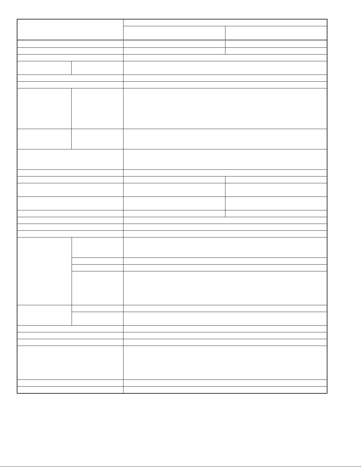
Alternative Check Method
Plug the AC line cord directly into the AC outlet (do not
use a line isolation transformer during this check.).
Use an AC voltmeter having 1000 ohms per volt or
more sensitivity in the following manner. Connect a
1500Ω 10W resistor paralleled by a 0.15µF AC-type
capacitor between an exposed metal part and a known
good earth ground (water pipe, etc.). Measure the AC
voltage across the resistor with the AC voltmeter. Move
the resistor connection to each exposed metal part,
particularly any exposed metal part having a return path
to the chassis, and measure the AC voltage across
the resistor. Now, reverse the plug in the AC outlet and
repeat each measurement. Any voltage measured
must not exceed 0.75V AC (r.m.s.). This corresponds
to 0.5mA AC (r.m.s.).
However, in tropical area, this must not exceed 0.3V AC
(r.m.s.). This corresponds to 0.2mA AC (r.m.s.).
AC VOLTMETER
(HAVING 1000Ω/V,
OR MORE SENSITIVITY)
0.15µF AC-TYPE
PLACE THIS PROBE
1500Ω 10W
GOOD EARTH GROUND
ON EACH EXPOSE
ME TA L PA RT
(No.YA101) 1-3
Page 4
1.2 INSTALLATION
1.2.1 HEAT DISSIPATION
If the heat dissipation vent behind this unit is blocked, cooling
efficiency may deteriorate and temperature inside the unit will
rise. The temperature sensor that protects the unit will be
activated when internal temperature exceeds the predetermined level and power will be turned off automatically.
Therefore, please make sure pay attention not to block the heat
dissipation vent as well as the ventilation outlet behind the unit
and ensure that there is room for ventilation around it.
SPACE REQUIRED FOR INSTALLATION
1.2.2 INSTALLATION REQUIREMENTS
Ensure that the minimal distance is maintained, as specified
below, between the unit with and the surrounding walls, as well
as the floor etc.
Install the unit on stable flooring or stands.
Take precautionary measures to prevent the unit from tipping in
order to protect against accidents and earthquakes.
150 mm or
150 mm
more
200 mm or
200 mm
more
50 mm
50 mm or more
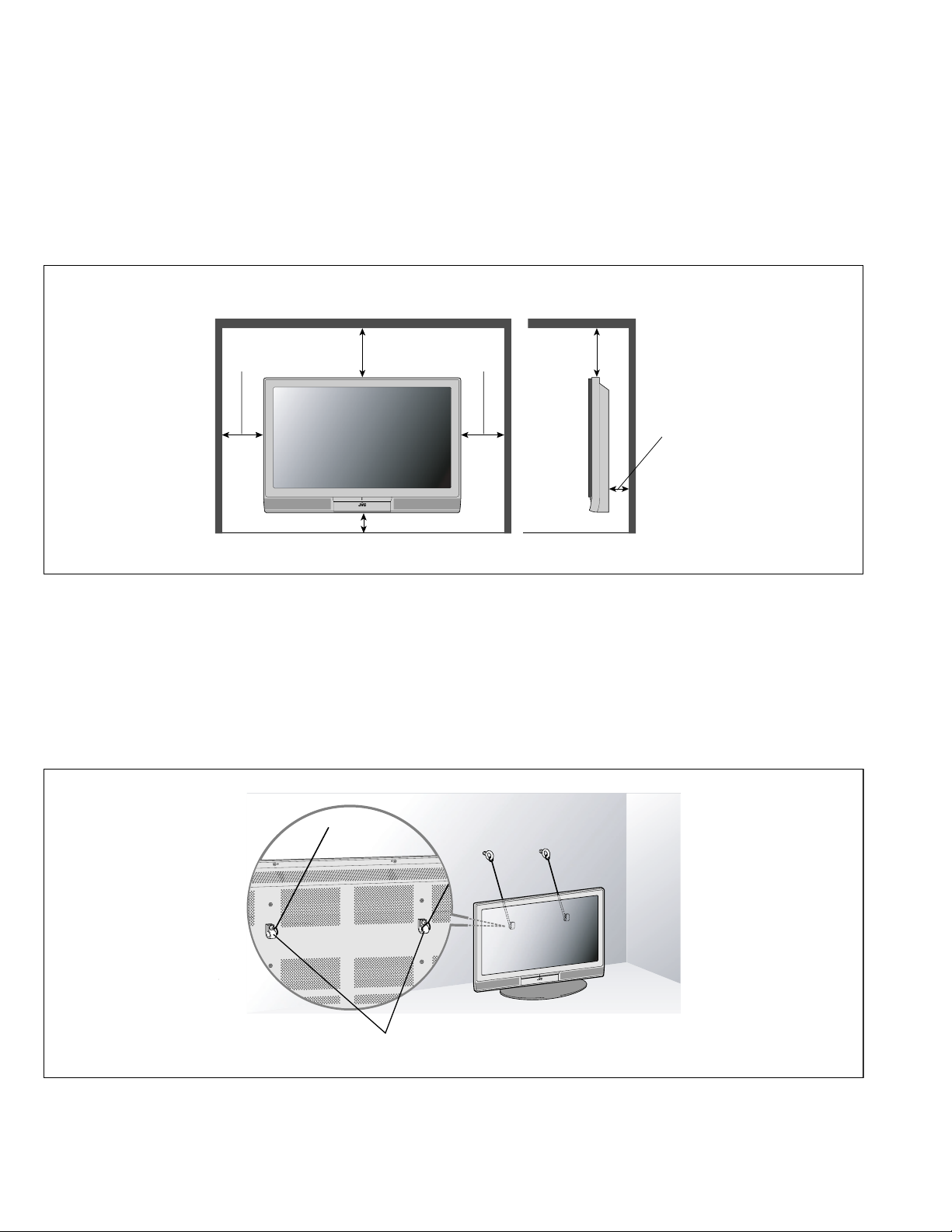
1.2.3 FALL TIP PREVENTION MEASURES
Take precautionary measures to prevent the unit from falling or
tipping to protect against emergencies such as earthquakes as
well as accidents.
Fasten the supplied hook for tip fall prevention using the screws,
also supplied, behind the display unit, and use them together
with durable cords (to be purchased separately) to secure the
unit to a robust part such as the wall surface or pillars.
150 mm
or more
150 mm
200 mm
200 mm
or more
50 mm
50 mm or more
1-4 (No.YA101)
The supplied hook for tipfall prevention
Page 5

1. 3 PRECAUTIONS REGARDING PDP
1.3.1 PRECAUTIONS DURING NOTES FOR TRANSPORTATION
When transporting the unit, pressure exerted on the internal
PDP (Plasma Display Panel) due to improper handling (such
as tossing and dropping) may cause damages even when the
unit is carefully packed. To prevent accidents from occurring
during transportation, pay careful attention prior to delivery such
as through explaining the handling instructions to transporters.
Ensure that the following requirements are met during
transportation, as the PDP of this unit is made of glass and
therefore fragile:
(1) Avoid vibrations and impacts
The unit may be broken if it is toppled sideways even
when properly packed. Ensure that the unit is carried by at
least 2 persons and pay careful attention not to exert any
vibration or impact on it.
(2) Do not place equipment horizontally
Ensure that it is placed upright and not horizontally during
transportation and storage as the PDP is very vulnerable
to lateral impacts and may break easily under such
circumstances.
During transportation, ensure that the unit is loaded along
the traveling direction of travel of the vehicle, and avoid
stacking them on one another.
For storage, ensure that they are stacked in 2 layers or
less even when placed upright.
1.3.2 RESIDUAL IMAGE / BURN-IN ON SCREEN
Like CRTs, “burn-in” may occur when a same image is
continuously displayed over an extended period of time.
As this may also shorten the life span of the PDP. Therefore, turn
off the display when not in use, scroll the screen, make use
of screen-savers, or allow even distribution on the display by
inverting the brightness, switching to complementary colors or
inserting animated images at periodic intervals.
As burn-in is more likely to occur with high brightness and contrast
settings, try to use neutral gradations or medium tone colors.
Burn-in does not occur in the case of animated images.
When switching to another image after continuous display of
the previous image, residual images may become prominent,
as luminance in a part of the display is higher than the other
parts.
This is not a defect but is because due to the discharge surface
of the lighted portion has become being relatively activated and
its luminance higher than the unlighted parts.
1.3.4 OPTICAL FILER (PANEL FILTER)
Avoid placing the unit under direct sunlight over a prolonged
period of time. This may cause the optical filter to deteriorate in
quality and color.
Clean the filter surface by wiping it softly lightly with outing flannels
a soft and lightly fuzz cloth (such as flannel).
Do not use solvents such as benzine or thinner to wipe the filter
surface. This may cause the filter to deteriorate in quality or the
coating on the surface to come off.
As the filter surface is fragile., do not scratch or hit it with hard
materials.
1.3.5 NOTES PRECAUTIONS FOR REPLACEMENT OF
EXTERIOR PARTS
Take note of the following when replacing exterior parts (back
REAR COVER, FRONT PANEL, optical filter)
• Do not exert pressure on the front of the PDP (glass surface).
• Pay careful attention not to scratch or stain the front of the PDP
(surface) with hands.
• When replacing exterior parts, the front of the PDP should be
placed facing downward. Place a mat, etc. underneath to avoid
causing scratches to the front surface. However, never use
materials that are too soft (such as blanket cloth). If
replacement is made with the PDP surface facing downward
and in contact with the blanket, pressure may be exerted on
the PDP, thus causing damages to it.
1.3.3 INFRARED RAYS
Near Near-infrared rays (800nm to 1000nm) are emitted from
the front of the panel, and this may give rise to malfunctions in
infrared remote controls or communication systems placed near
it. In this case, avoid direct infrared rays (and reflected rays in
some cases) from the screen by either changing the direction of
the unit or other infrared systems or securing a longer keeping
a distance from the screen.
(No.YA101) 1-5
Page 6
SECTION 2
SPECIFIC SERVICE INSTRUCTIONS
2.1 FEATURES
2.1.1 HIGH-DEFINITION IMAGE TECHNOLOGY (DIST)
• DIST (Digital Image Scaling Technology)
Employs an interpolation method that doubles the scanning
lines to realize 480-line flickerfree picture making it especially
suitable for reproducing high-resolution pictures even on largescreen displays.
2.1.2 MAIN FUNCTION
•
DIGITAL VNR
The DIGITAL VNR function cuts down the amount of noise in
original picture. There are three function settings of AUTO,MIN
and MAX.
• Super DigiPure
This function uses the latest technology to give viewer a natural
looking picture.
It consist of DigiPure and picture motion compensation function.
•
PULL DOWN
This function displays a cinema film picture more smoothly
and naturally on the screen.
•
COLOUR MANAGEMENT
This function ensures dull colours are compensated to produce
natural hues.
•
PICTURE MANAGEMENT
This function makes it easier to see the dark areas when a
picture has many dark areas, and makes it easier to see the
bright areas when a picture has many bright areas.
• Sleep Timer
Setting for situations such as falling asleep while watching TV,
and for prevention against forgetting to turn off the TV. The
power supply of the TV will be cut off automatically when the
time exceeds the set up timing (maximum 2 hours).
• CINEMA SURROUND function
This function makes the speaker sounds like in a wider
ambience.
• A.H.B. (Active Hyper Bass)
Used when you want to emphasize the bass sound.
• BBE
You can use the BBE function to enjoy easyto-listen sound that
is faithful to the original sound recorded.
• Teletext function
The teletext broadcast can be viewed and the teletext pages
can be stored in memory.
2.1.3 ASPECT CONTROL
The screen size can be changed according to the picture aspect
ratio.
• ZOOM function
Desired screen size (AUTO/REGULAR / PANORAMIC / 14:9
ZOOM / 16:9 ZOOM / 16:9 ZOOM SUBTITLE / FULL) can be
selected.
2.1.4 MULTI-SCREEN FUNCTION
• Twin-pictures function
With the function, two pictures can be displayed at the Twin
pictures mode.
• Multi-picture function
With this function, one of multi-picture (12 pictures) can be
displayed at the same time.
• Freeze function
The images that are currently seen can be viewed on the memo
screen (still picture).
It is convenient for taking down notes like application address
and recipe of cooking program etc, while enjoying the current
program.
2. 2 MAIN DIFFERENCE LIST
Item
POWER CORD
POWER CORD
POWER CORD
1-6 (No.YA101)
PD-Z35DV4
PD-Z42DV4
QMPL050-250-K
QMPB560-180-JC
PD-Z35DV4/S
PD-Z42DV4/S
---
---
QMPB320-180-R
---
Page 7
2. 3 TECHNICAL INFORMATION
2.3.1 PDP STRUCTURE AND CHARACTERISTIC
This unit uses the flat type panel PDP (Plasma Display Panel), instead of the conventional CRT (Cathode Ray Tube), as a display unit.
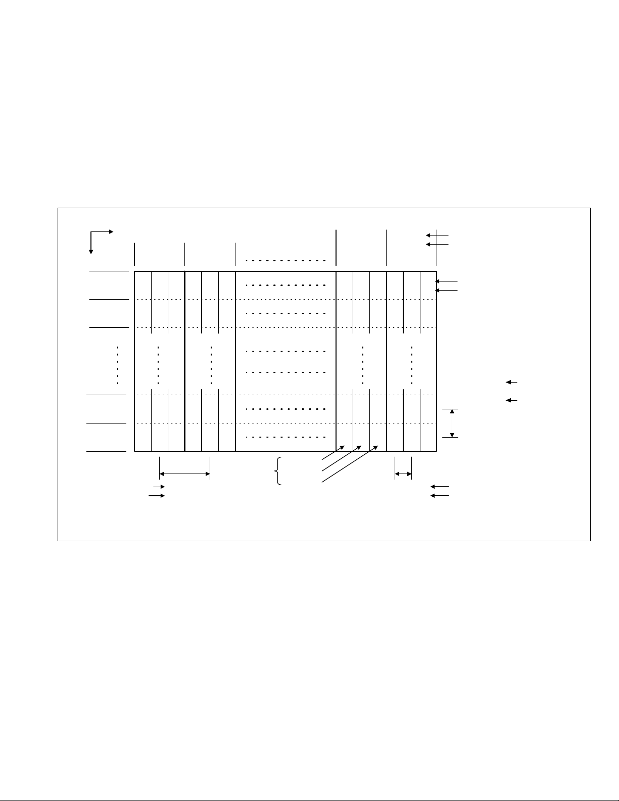
2.3.1.1 PIXEL (CELL) ARRAY
PDP is constructed by sealing the xenon, which emits neon and ultraviolet rays for discharging purpose, in between the electrodes
lay on the front glass substrate and rear glass substrate.
One pixel is composed of 3 RGB cells, with cell pitch of 0.365mm (1 pixel 1.095mm) [PD-Z42DV4, PD-Z42DV4/S] / 0.307 mm (1 plxel
0.921 mm) [PD-Z35DV4, PD-Z35DV4/S] horizontally and 1.110mm [PD-Z42DV4, PD-Z42DV4/S] / 0.921 mm [PD-Z35DV4, PDZ35DV4/S] vertically.
The cell is arrayed in each RGB color as shown in Fig. 1. One pixel is formed by interlacing each RGB color cell.
One cell size is 0.365mm [PD-Z42DV4, PD-Z42DV4/S] / 0.307 mm [PD-Z35DV4, PD-Z35DV4/S] horizontally and 1.110mm [PDZ42DV4, PD-Z42DV4/S] / 0.921 mm [PD-Z35DV4, PD-Z35DV4/S] vertically.
Direction
Vertically
No.1
Pixel line
No.2
Pixel line
No.479
Pixel line
No.480
Pixel line
PD-Z42DV4,
PD-Z42DV4/S
PD-Z35DV4,
PD-Z35DV4/S
Horizontally
No.1
Pixel
sequence
No.2
Pixel
sequence
B G R B G R
(R) (B) (R)(G) (G) (B) (R) (B) (R) (B)
BG
(R) (B) (R)(G) (G)
B
(R) (B) (R) (B) (R) (B) (R) (B)
B
(R) (B) (R) (B) (R) (B) (R) (B)
RBGR
(B) (R) (B) (R) (B)
G RBG R
(G) (G)
GRBGR
(G) (G)
1 pixel
(1 dot)
1.095mm
0.921 mm 0.307 mm
(Horizontally) Pixel pitch
B(R) Cell
G(G)
Cell
R(B) Cell
No.851 No.852
No.852
Pixel
sequence
B GRBG R
(G) (G)
BGRBGR
(G) (G)
G RBG R
B
(G) (G)
GRBGR
B
(G) (G)
0.365mm
(Horizontally) Cell pitch
No.853
Pixel
sequence
PD-Z42DV4, PD-Z42DV4/S
PD-Z35DV4, PD-Z35DV4/S
PD-Z42DV4, PD-Z42DV4/S
PD-Z35DV4, PD-Z35DV4/S
1.110 mm PD-Z42DV4,
PD-Z42DV4/S
0.921 mm PD-Z35DV4,
PD-Z35DV4/S
(Vertically)
Pixel pitch
(Cell pitch)
PD-Z42DV4, PD-Z42DV4/S
PD-Z35DV4, PD-Z35DV4/S
Fig.1
2.3.1.2 PIXEL DEFECTS
Though PDP is made by means of ultra precise technology, there are cases whereby not all pixels (cell) will function properly. In
some cases, there may be defective pixels that do not light at all or the ones that always light on.
There are 3 types of Pixel defects, [Bright Dot Defects], [Dark Dot Defects] and [Flicker Dot Defects], as defined respectively in the
following:
(1) Bright Dot Defects
Bright dot defect is a pixel cell that lights though it should not light.
The presence of bright dot defects can be confirmed by inputting a full black signal (pattern).
(2) Dark Dot Defects
Dark dot defect is a pixel cell that does not light, though it should light.
The presence of dark dot defects can be confirmed by inputting a 100% full white signal (pattern).
(3) Flicker Dot Defects
Flicker dot defect is a pixel cell that blinks though it should light or not light.
The presence of flicher dot defects can be confirmed by inputting a full black signal (pattern).
(No.YA101) 1-7
Page 8
2.3.2 CHASSIS CPU [DIGITAL SIGNAL PWB : IC7001] PIN FUNCTION
Pin
No.
Pin name I/O Function
Pin
No.
1 NC O Not used
2 P_MU O Video muting [Muting : H]
3 FUNC_LED O Not used
4 A_MU O Audio muting [Muting : H]
5 M_MU O Monitor audio muting [Muting : H]
6 PC_SW O PC i n p u t select [ON : H]
7 DIMMER_LED O Power LED dimmer control [Low dimmer : L]
8 NC O Not used
9 NC O Not used
10 NC O Not used
11 POW_LED O Power LED control [ON : H]
12 NC O Not used
13 SBT2 I Clock for main CPU communication
14 SBI2 I Data transmission for main CP U
communication
15 SBO2 O Data receive for main CP U communication
16 REQ O Request for main CPU communication
17 3.3V I 3.3V
18 NC O Not used
19 GND - GND
20 3.3V I 3.3V
21 NC O Not used
22 3.3V I 3.3V
23 OSCI I 16MHz for system clock
24 OSCO O 16MHz for system clock
25 3.3V I 3.3v
26 NC O Not used
27 A92_RST O 3D YC separation reset [Reset : L]
28 NC O Not used
29 LIP_RST O Not used
30 NC O Not used
31 NC I Not used
32 NC O Not used
33 MDR_CON I Not used
34 3.3V I 3.3V
35 NC O Not used
36 DsyncSW2 O Not used
37 NC O Not used
38 NC O Not used
39 HOTPLUG I Not used
40 MECA_SW I Power switch monitor [ON : L]
41 MAIN_POW O Main power control [ON : L]
42 MSP_RESET O Multi sound processor reset [Reset : H]
43 0V - GND
44 NC I Not used
45 AFT1 I AFT detection [Detection : H]
46 NC I Not used
47 NC I Not used
48 NC O Not used
49 NC O Not used
50 NC I Not used
51 NC O Not used
52 NC I Not used
53 NC O Not used
54 3.3V I 3.3V
55 PDP_TX O PDP communication for panel CPU
56 PDP_RX I PDP communication for panel CPU
57 SDA0 I/O I2C bus data (for chassis memory)
58 SCL0 O I2C bus clock (for chassis memory)
59 SDA_DVI I/O Not used
60 SCL_DVI I/O Not used
61 GND - GND
62 NC I Not used
63 NC I Not used
64 NC I Not used
Pin name I/O Function
65 NC I Not used
66 3.3V I 3.3V
67 NC O Not used
68 NC O Not used
69 NC O Not used
70 NC O Not used
71 NC O Not used
72 NC O Not used
73 SBD5 I/O Flash writing for chassis CPU
74 SBT5 I Flash writing for chassis CPU
75 3.3V I 3.3V
76 NC I Not used
77 REMOCON I Remote control
78 V_SYNC I Vertical sync
79 WAKEUP_SHM I
Sleep state release for chassis CPU
[Relese : L]
80 POWERGOOD I Power error detection [Detection : H]
81 REC_LED O Stand-by power LED control [Stand-by :H]
82 RST I Chassis CPU reset [Reset : L]
83 3.3V I 3.3V
84 SCL3A O I
2
C bus clock (for 3D YC separation,
colour management / OSD composition /
RGB process, U / V frontend)
2
85 SDA3A I/O I
C bus data (for 3D YC separation,
colour management / OSD composition /
RGB process, U / V frontend)
2
86 SCL3B O I
C bus clock (for multi sound process,
video / audio select, colour demod. /
sync sep., 3 line comb filter, component
video / audio select, sync sep. / SW /
detect)
2
87 SDA3B I/O I
C bus data (for multi sound process, video
/ audio select, colour demod. / sync sep.,
component video / audio select, sync sep. /
SW / detect)
88 NC O Not used
89 NC O Not used
90 NC O Not used
91 DVI_RST O Not used
92 GND - GND
93 SCL5055 O I2C bus clock (for DIST)
94 NC O Not used
95 SDA5055 I/O I2C bus data (for DIST)
96 NC O Not used
97 NC O Not used
98 15K/OTH O Y signal select for 3D YC separation
[525i : H / other : L]
99 DsyncSW1 O Not used
100 JCC5057_BUSY I Busy for Colour management / RGB
prosess / OSD composition [Busy : H]
1-8 (No.YA101)
Page 9
2.3.3 MAIN CPU [DIGITAL SIGNAL PWB : IC7501] PIN FUNCTION
Pin
No.
10 OSDB4 O Blue for OSD
11 TV-LINK I Not used
12 RX_BUSY(Sirial) O Request for chassis CPU communication
13 VSS33 - GND
14 VDD33 I 3.3V
15 TV_LINK_OUT O Not used
16 A20 O Program ROM address for main CPU
17 A19 O Program ROM address for main CPU
18 A18 O Program ROM address for main CPU
19 A17 O Program ROM address for main CPU
20 VSS25 - GND
21 VDD25 I 2.5V
22 A16 O Program ROM address for main CPU
23 A8 O Program ROM address for main CPU
24 A7 O Program ROM address for main CPU
25 A9 O Program ROM address for main CPU
26 A6 O Program ROM address for main CPU
27 A5 O Program ROM address for main CPU
28 A10 O Program ROM address for main CPU
29 A11 O Program ROM address for main CPU
30 A12 O Program ROM address for main CPU
31 VSS33 - GND
32 VDD33 I 3.3V
33 A4 O Program ROM address for main CPU
34 A3 O Program ROM address for main CPU
35 A2 O Program ROM address for main CPU
36 A1 O Program ROM address for main CPU
37 A0 O Program ROM address for main CPU
38 A13 O Program ROM address for main CPU
39 A14/RAS O Program ROM address for main CPU
40 A15/CAS O Program ROM address for main CPU
41 VSS33 - GND
42 VDD33 I 3.3V
43 MEMCLK O Clock for memory
44 CSSDRAM O Chip select for memory
45 CLKEN O Clock enable for memory
46 CSROM O Chip select for memory
47 RD O Read for memory
48 UDQM O Control buffer of memory
49 LDQM O Control buffer of memory
50 WR O Write for memory
51 D15 I/O Program ROM data for main CPU
52 VSS33 - GND
53 VDD33 I 3.3V
54 D7 I/O Program ROM data for main CPU
55 D0 I/O Program ROM data for main CPU
56 D14 I/O Program ROM data for main CPU
57 D8 I/O Program ROM data for main CPU
58 D6 I/O Program ROM data for main CPU
59 D1 I/O Program ROM data for main CPU
60 VSS33 - GND
61 VDD33 I 3.3V
62 D13 I/O Program ROM data for main CPU
63 D9 I/O Program ROM data for main CPU
64 D5 I/O Program ROM data for main CPU
65 D2 I/O Program ROM data for main CPU
Pin name I/O Function
1 TCK I Test purpose
2 TMS I Test purpose
3 TDI I Test purpose
4 TDO O Test purpose
5 NC O Not used
6 OSDB0 O Blue for OSD
7 OSDB1 O Blue for OSD
8 OSDB2 O Blue for OSD
9 OSDB3 O Blue for OSD
Pin
No.
66 D12 I/O Program ROM data for main CPU
67 D10 I/O Program ROM data for main CPU
68 VSS33 - GND
69 VDD33 I 3.3V
70 D4 I/O Program ROM data for main CPU
71 D3 I/O Program ROM data for main CPU
72 D11 I/O Program ROM data for main CPU
73 RSTIN I Reset
74 POWER O
75
76 REMOCON I Remote control
77 PIX CLOCK I Clock for OSD
78 OSDR0 O Red for OSD
79 OSDR1 O Red for OSD
80 OSDR2 O Red for OSD
81 OSDR3 O Red for OSD
82 MRST(Sirial) O Data transmission for chassis CP U
83 MTSR(Sirial) I Data receive for chassis CPU communication
84 VSS33 - GND
85 VDD33 I 3.3V
86 VSS25 - GND
87 VDD25 I 2.5V
88 MICON TX O Communication for adjustment
89 MICON RX O Communication for adjustment
90 OSDR4 O Red for OSD
91 CLK(Sirial) O Clock for chassis CPU communication
92 OSDG0 O Green for OSD
93 OSDG1 O Green for OSD
94 OSDG2 O Green for OSD
95 OSDG3 O Green for OSD
96 OSDG4 O Green for OSD
97 OSDG5 O Green for OSD
98 SCL3A O I2C b us cl ock ( for main memory)
99 SDA3A I/O I2C bus Data (for main memory)
100 TEXT / OTHER O Teletext signal select
101 IRQ(IDTV) O Not used
102 V_PULSE I Vertical sync
103 H_PULSE I Horizontal sync
104 (COR/RSTOUT) O Not used
105 Ys O Ys for OSD / Teletext
106 VDD33 I 3.3V
107 VSS33 - GND
108 XTAL1 I 6MHz for system clock
109 XTAL2 O 6MHz for system clock
110 VSSA - GND
111 VDDA I 2.5V
112 R O R for OSD / Teletext
113 G O G for OSD / Teletext
114 B O B for OSD / Teletext
115 VSSA - GND
116 VDDA I 2.5V
117 CVBS I Video for Teletext
118 VSSA - GND
119 VDDA I 2.5V
120 GND I GND
121 CVBS I Video for Teletext
122 VSSA - GND
123 VDDA I 2.5V
124 F_KEY_1 I Key scan data 1 [ON : H]
125 F_KEY_2 I Key scan data 2 [ON : H]
126 POWER_KEY I Main power ON / OFF control [ON : L]
127 NC I Not used
128 (TMODE) I Test purpose
Pin name I/O Function
Sleep state release for chassis CPU [Relese : L]
ID_TV_POWER(IDTV)
O Not used
communication
[Analog RGB : H / Digital RGB : L]
(No.YA101) 1-9
Page 10
2.3.4 PANEL CPU [INTERFACE PWB : IC807] PIN FUNCTION
Pin
No.
Pin name I/O Function
1 SYSTEM0 I PDP size select [1.75V : 42V VGA
3.25V : 35V VGA]
2 SYSTEM3 I PDP maker select [0V : SAMSUNG
3.25V : NEC]
3 AVCC I 5.0V
4 X2 - Not used
5 X1 - GND
6 VCL - GND
7 RES I Reset [Reset : L]
8 TEST I GND
9 VSS - GND
10 OSC2 O 16MHz for system clock
11 OSC1 I 16MHz for system clock
12 VCC I 5.0V
13 PW_LOB O Power control [ON : L]
14 PANEL_PW_ON O Panel power control [ON : L]
15 TALK_RST O Not used
16 CODEC_RST O Not used
17 I2C_STOP O I2C bus stop control [Stop : L]
18 NC O Not used
19 PSCK O Not used
20 PLE O Not used [PD-Z42DV4, PD-Z42DV4/S] /
PDP communication for DVI format
conversion [PD-Z35DV4, PD-Z35DV4/S]
21 CLE O Not used
22 PSSC O Not used
23 SDA1 I/O I2C bus data (for panel memory)
24 FAN O Not used
25 SCL1 O I2C bus clock (for panel memory)
26 SDA0 I/O
I2C bus data (for BBE / surround / audio control,
temp. sensor)
27 SCL0 O
I2C bus clock (for BBE / surround / audio control,
temp. sensor)
28 SDA2 / SDATA I/O I2C bus data (for PDP communication)
29 SCL2 / SCK O I2C bus clock (for PDP communication)
30 LE O Not used [PD-Z42DV4, PD-Z42DV4/S] /
PDP communication for DVI format
conversion [PD-Z35DV4, PD-Z35DV4/S]
31 SDA3 I/O Not used
32 SCL3 O Not used
33 NC O Not used
34 NC O Not used
35 NMI I Port for writing on board control [Writing : L]
36 A_MU O Audio muting [Muting : H]
37 (HD) I Not used
38 ON_TIMMER O Not used
39 REMO I Not used
40 POWERLED O Not used
41 P85 I Emulator connection / Port for writing on
board [Writing : H]
42 P86 I Emulator connection
43 P87 I Emulator connection
44 SCK3 O Port for writing on board
45 RXD I Port for writing on board
46 TXD O Port for writing on board
47 AC_DET / ALARM I AC power frequency detection
[Detection : H] [PD-Z42DV4, PD-Z42DV/S] /
PDP communication for DVI format
converstion [PD-Z35DV4, PD-Z35DV4/S]
48 NC O Not used
49 RXD2 I Data receive for chassis CPU communication
50 TXD2 O Data transmission for chassis CPU
communication
51 NC O Not used
52 MECA_SW I Not used
Pin
No.
Pin name I/O Function
53 VD I Vertical sync
54 REC_DET I Not used
55 I2C_READY / PSS I PDP I
2
C communication select
[Prohibition : L / Permission : H]
[PD-Z42VD4, PD-Z42DV4/S] /
PDP communication for DVI format
converstion [PD-Z35DV4, PD-Z35DV4/S]
56 FAN_LOCK I Not used
57 SYSTEM2 I Not used
58 SYSTEM 1 I Not used
59 THEM_DET I Temp. sensor detection [Detection : H]
60 (AMP_PRO2) - GND
61 AMP_PRO1 I Not used
62 EE_CDS I Not used
63 KEY_IN1 I Not used
64 KEY_IN2 I Not used
1-10 (No.YA101)
Page 11
SECTION 3
DISASSEMBLY
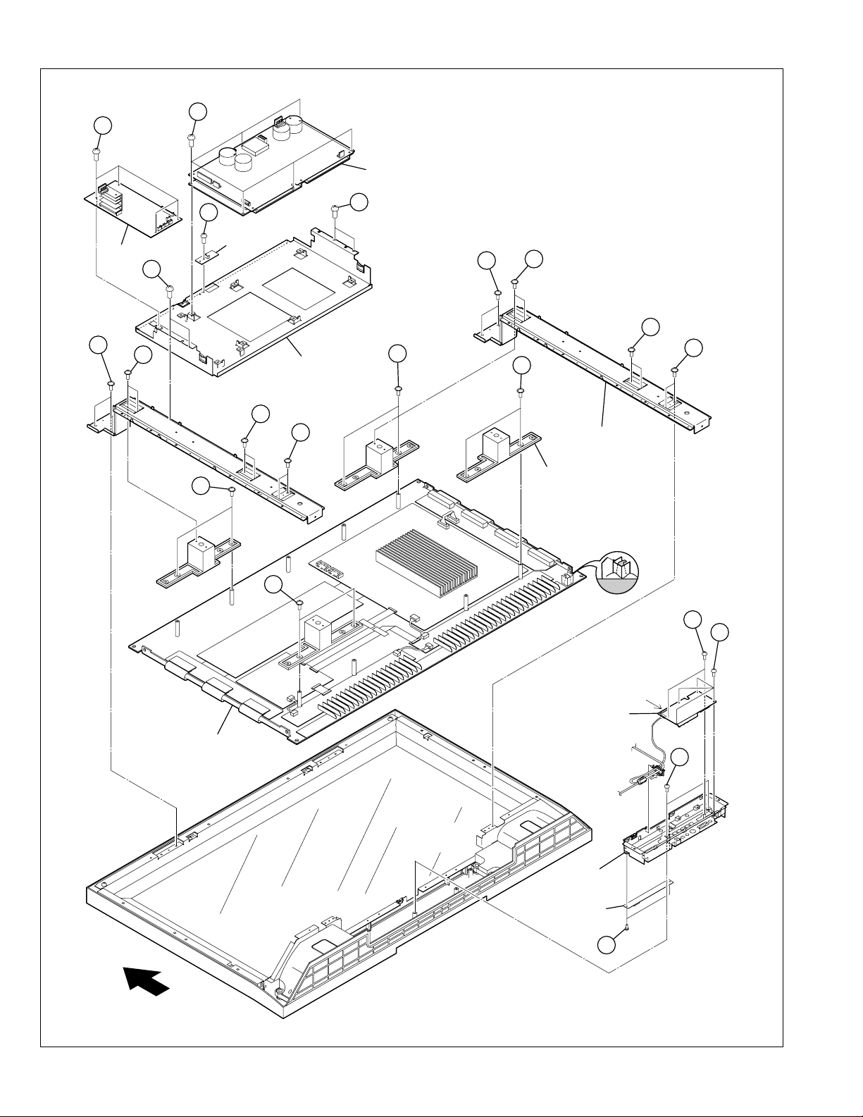
3.1 DISASSEMBLY PROCEDURE [PD-Z42DV4, PD-Z42DV4/S]
CAUTION:
• When exchanging parts etc. with the front side (PDP side)
facing down, please place a protection sheet below before
starting, so as to prevent scratches on the front side.
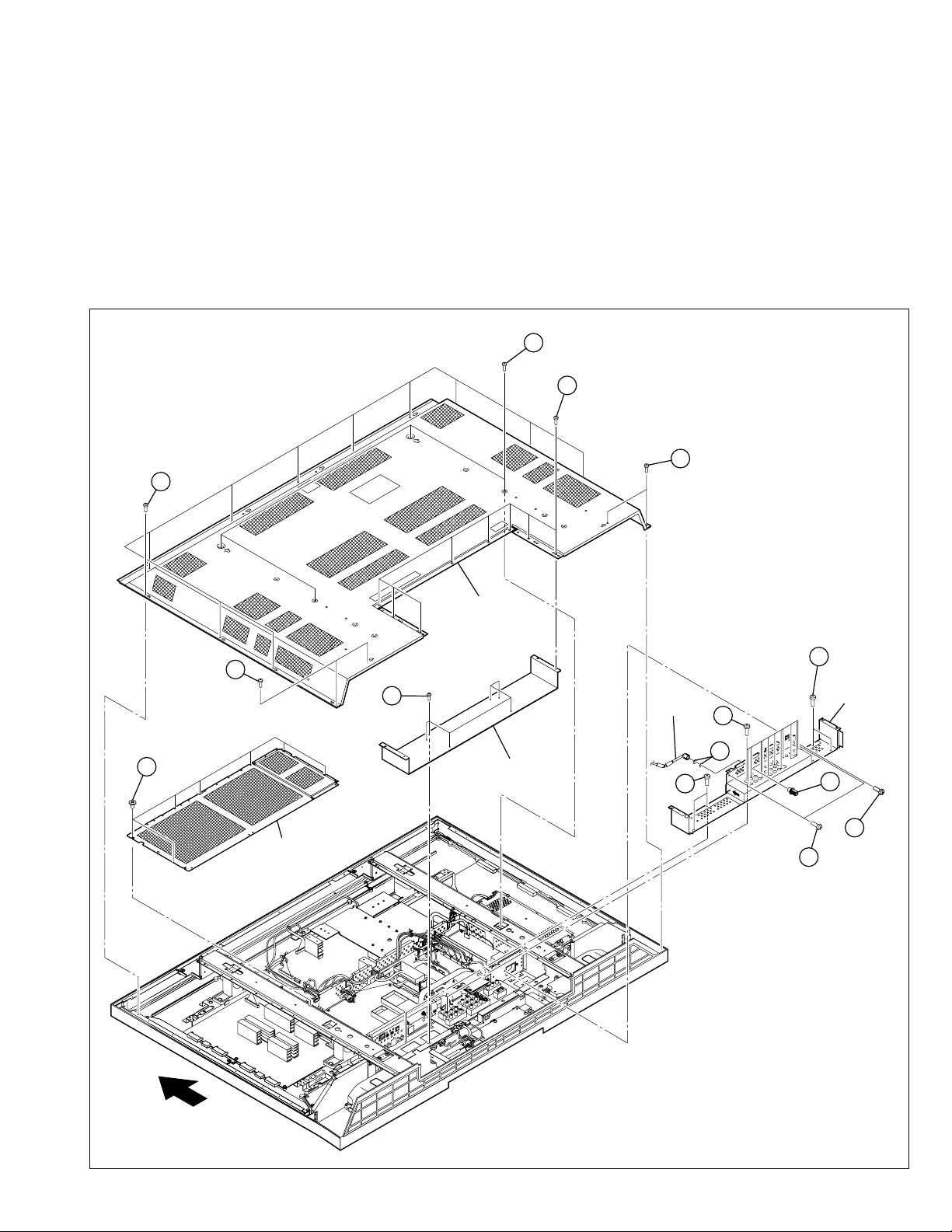
3.1.1 REMOVING THE REAR COVER (Fig.1)
(1) Remove the power cord.
(2) Remove the 15 screws [A], the 4 screws [B] and the 8
screws [C], and remove the REAR COVER.
(x11)
A
3.1.2 REMOVING THE TERMINAL COVER AND CENTER COVER
(Fig.1)
• Remove the REAR COVER.
(1) Remove the 7 screws [D], and remove the CHASSIS
SHIELD COVER.
(2) Remove the 6 screws [E], and remove the CENTER
COVER.
(3) Disconnect the COAXIAL CABLE.
(4) Remove the 6 screws [F], the 12 screws [G], the 1 screw
[H], and the 1 connector [I], and remove the TERMINAL
COVER.
A
(x4)
C
(x8)
(x2)
B
REAR COVER
(x2)
B
(x2)
(x6)
E
(x7)
D
CHASSIS
SHIELD
COVER
CENTER COVER
COAXIAL
CABLE
(x12)
F
(x2)
G
I
F
TERMINAL
COVER
I
(x2)
F
H
TOP
Fig. 1
(No.YA101) 1-11
Page 12

3.1.3 REMOVING THE AUDIO PWB (Fig. 2)
• Remove the REAR COVER.
(1) Remove the 4 screws [J], and remove the AUDIO CHASSIS
COVER.
(2) Disconnect the connectors [CN600B], [CN600C],
[CN600Y], [CN60SL], [CN60SR] from the AUDIO PWB.
(3) Remove the 4 screws [K], and remove the AUDIO PWB.
NOTE:
• It is advisable to take note of the connecting location
(connector number) of the removed connectors.
3.1.4 REMOVING THE AV JACK PWB (Fig.2)
• Remove the REAR COVER.
• Remove the CENTER COVER.
• Remove the CHASSIS SHIELD COVER.
• Remove the TERMINAL COVER.
(1) Disconnect the connectors [CN0J01], [CN0J02] from the
AV JACK PWB.
(2) Remove the 4 screws [L], and remove the AV JACK PWB.
NOTE:
• It is advisable to take note of the connecting location
(connector number) of the removed connectors.
3.1.5 REMOVING THE INTERFACE PWB (Fig.2)
• Remove the REAR COVER.
• Remove the CENTER COVER.
• Remove the CHASSIS SHIELD COVER.
• Remove the TERMINAL COVER.
(1) Disconnect the connectors [CN00B], [CN00C], [CN00Q],
[CN00G], [CN00T], [CN00V], [CN00X], [CN0FC], [CN0FN]
from the INTERFACE PWB.
(2) Remove the 2 screws [M], and withdraw the INTERFACE
PWB.
NOTE:
• It is advisable to take note of the connecting location
(connector number) of the removed connectors.
3.1.6 REMOVING THE REGULATOR PWB (Fig.2)
• Remove the REAR COVER.
• Remove the CENTER COVER.
• Remove the CHASSIS SHIELD COVER.
• Remove the TERMINAL COVER.
• Remove the INTERFACE PWB.
(1) Disconnect the connectors [CN003], [CN008], [CN00D]
from the REGULATOR PWB.
(2) Remove the 4 screws [N], and remove the REGULATOR
PWB.
NOTE:
• It is advisable to take note of the connecting location
(connector number) of the removed connectors.
3.1.7 REMOVING THE LINE FILTER PWB (Fig.2)
• Remove the REAR COVER.
• Remove the CENTER COVER.
• Remove the CHASSIS SHIELD COVER.
• Remove the TERMINAL COVER.
• Remove the INTERFACE PWB.
(1) Remove the 1 screw [O] and the 1 screw [P], and remove
the AC INLET PANEL.
(2) Disconnect the connector [CN8001] from the MAIN POWER
PWB.
(3) Remove the 1 screw [Q], the 1 screw [R] and the 2 screws
[S], and remove the LINE FILTER PWB.
NOTE:
• It is advisable to take note of the connecting location
(connector number) of the removed connectors.
1-12 (No.YA101)
3.1.8 REMOVING THE RECEIVER PWB (Fig.2)
• Remove the REAR COVER.
• Remove the CENTER COVER.
• Remove the CHASSIS SHIELD COVER.
• Remove the TERMINAL COVER.
(1) Disconnect the connectors [CN00A], [CN00T] from the
RECEIVER PWB.
(2) Withdraw the RECEIVER PWB.
NOTE:
• It is advisable to take note of the connecting location
(connector number) of the removed connectors.
3.1.9 REMOVING THE ANALOG SIGNAL PWB (Fig.2)
• Remove the REAR COVER.
• Remove the CENTER COVER.
• Remove the CHASSIS SHIELD COVER.
• Remove the TERMINAL COVER.
• Remove the RECEIVER PWB.
(1) Disconnect the connectors [CN00F], [CN00G], [CN0J01],
[CN0J02] from the ANALOG SIGNAL PWB.
(2) Remove the 4 screws [T], and remove the ANALOG SIGNAL
PWB.
NOTE:
• It is advisable to take note of the connecting location
(connector number) of the removed connectors.
3.1.10 REMOVING THE DIGITAL SIGNAL PWB (Fig.2)
• Remove the REAR COVER.
• Remove the CENTER COVER.
• Remove the CHASSIS SHIELD COVER.
• Remove the TERMINAL COVER.
(1) Disconnect the connectors [CN001], [CN002], [CN003],
[CN0FC], [CN0LV2] from the DIGITAL SIGNAL PWB.
(2) Remove the 5 screws [U], and remove the DIGITAL SIGNAL
PWB.
NOTE:
• It is advisable to take note of the connecting location
(connector number) of the removed connectors.
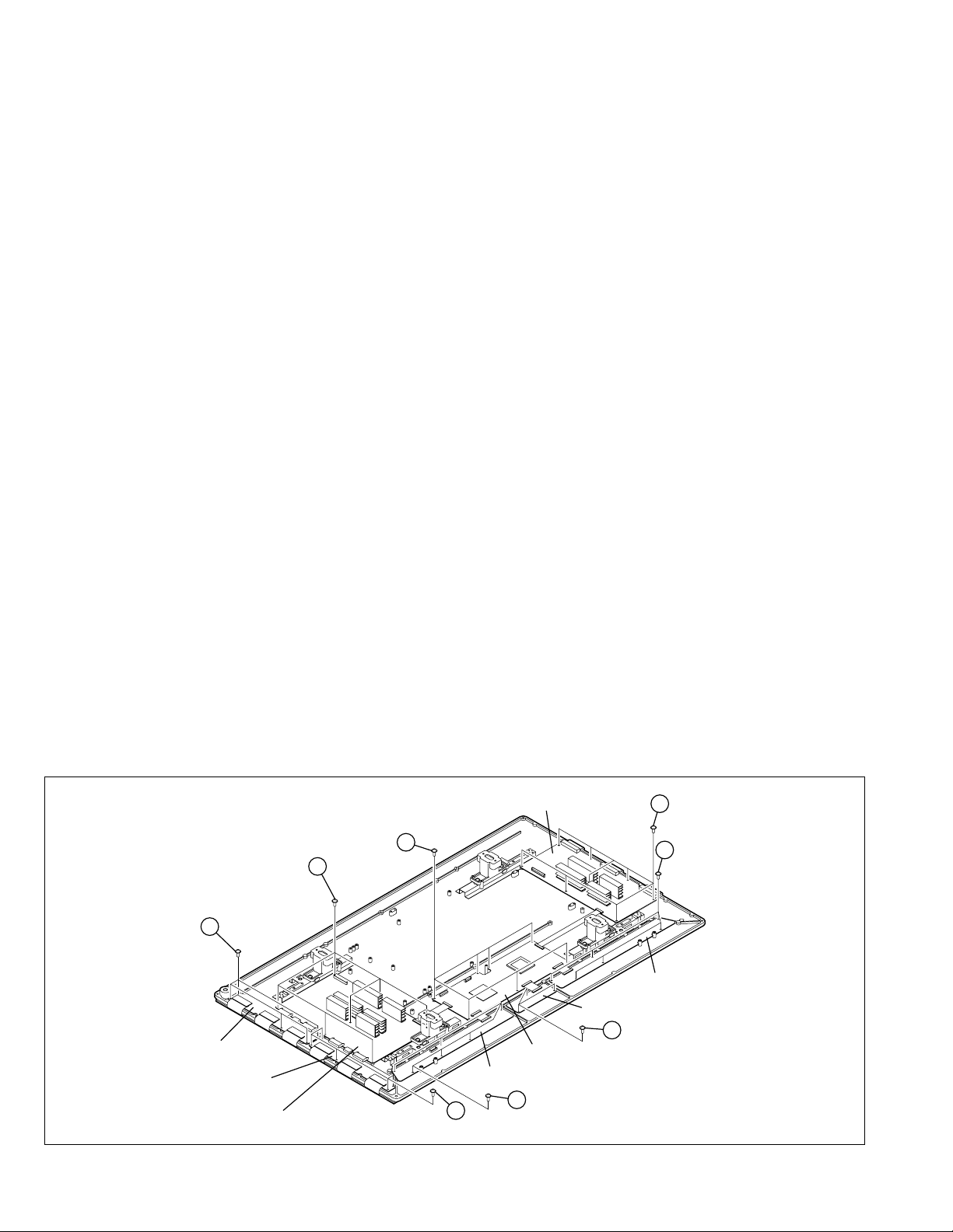
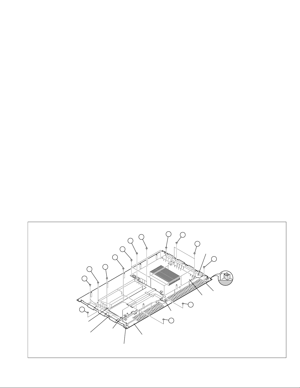
3.1.11 REMOVING THE MAIN BASE, CHASSIS BASE AND AUDIO
PWB BASE (Fig.2)
• Remove the REAR COVER.
• Remove the CENTER COVER.
• Remove the CHASSIS SHIELD COVER.
• Remove the TERMINAL COVER.
• Remove the AUDIO PWB.
• Remove the AV JACK PWB.
• Remove the INTERFACE PWB.
• Remove the REGULATOR PWB.
• Remove the LINE FILTER PWB.
• Remove the RECEIVER PWB.
• Remove the ANALOG SIGNAL PWB.
• Remove the DIGITAL SIGNAL PWB.
(1) Remove the 1 screw [V], and remove the DIGITAL
TERMINAL COVER.
(2) Remove the 1 screw [W].
(3) Lift the MAIN BASE upright and remove it.
(4) Remove the 2 screws [X], and remove the CHASSIS BASE.
(5) Remove the 1 screw [Y], and remove the AUDIO PWB BASE.
Page 13
RECEIVER PWB
INTERFACE PWB
(x4)
N
M
d
(x2)
Q
S
(x2)
R
ANALOG
SIGNAL PWB
(x5)
U
DIGITAL
SIGNAL
PWB
DIGITAL TEMINAL
COVER
e
d
MAIN BASE
X
c
b
T
(x4)
REGULATOR
PWB
W
LINE FILTER
a
PWB
L
(x4)
c
b
O
X
AC INLET
PANEL
a
P
CHASSIS BASE
Y
AV JACK PWB
J
(x4)
K
(x4)
AUDIO CHASSIS
COVER
AUDIO PWB
AUDIO PWB BASE
V
TOP
Fig. 2
(No.YA101) 1-13
Page 14

3.1.12 REMOVING THE FRONT CONTROL PWB (Fig.3)
• Remove the REAR COVER.
• Remove the CENTER COVER.
(1) Remove the 4 screws [Z] and the 2 screws [a].
(2) Disconnect the connectors [CN00F], [CN00T] from the
FRONT CONTROL PWB.
(3) Remove the FRONT CONTROL PWB.
NOTE:
• It is advisable to take note of the connecting location
(connector number) of the removed connectors.
3.1.13 REMOVING THE FRONT LED PWB (Fig.3)
• Remove the REAR COVER.
• Remove the CENTER COVER.
• Remove the FRONT CONTROL COVER.
(1) Remove the 2 screws [b], and withdraw the FRONT PWB
BASE.
(2) Disconnect the connector [CN00X] from the FRONT LED
PWB.
(3) Remove the 2 screws [c], and remove the FRONT LED
PWB.
NOTE:
• It is advisable to take note of the connecting location
(connector number) of the removed connectors.
3.1.14 REMOVING THE TEMP. SENSOR PWB (Fig.3)
• Remove the REAR COVER.
(1) Disconnect the connector [CN00V] from the TEMP.
SENSOR PWB.
(2) Remove the 1 screw [d], and remove the TEMP. SENSOR
PWB.
NOTE:
• It is advisable to take note of the connecting location
(connector number) of the removed connectors.
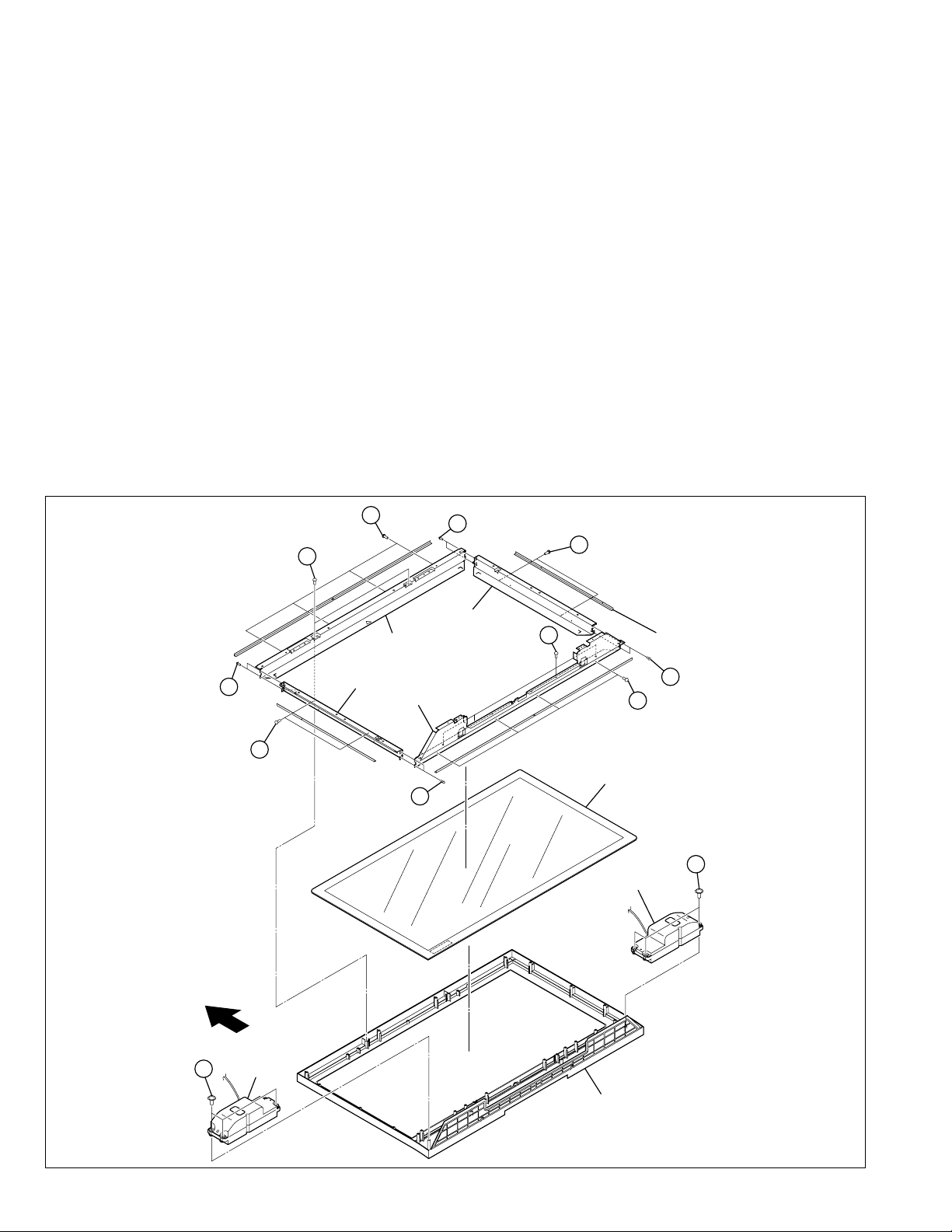
3.1.17 REMOVING THE PDP UNIT (Fig.3)
• Remove the REAR COVER.
• Remove the CENTER COVER.
• Remove the CHASSIS SHIELD COVER.
• Remove the TERMINAL COVER.
• Remove the MAIN BASE, CHASSIS BASE and AUDIO PWB
BASE (with each PWB affixed on the MAIN BASE, CHASSIS
BASE and AUDIO PWB BASE).
• Remove the TEMP. SENSOR PWB.
• Remove the MAIN POWER PWB.
• Remove the SUB POWER PWB.
(1) Remove the 8 screws [g] and the 8 screws [h], and remove
the BACK FRAME.
(2) Lift the PDP UNIT upright and remove it with enough care
not to impose shock to the PDP UNIT.
NOTE:
• It is advisable to take note of the connecting location
(connector number) of the removed connectors.
CAUTION:
• Two or more people are required to remove the PDP UNIT.
• The gas pouring port is covered with the protection material.
In operation, be careful not to damage the gas pouring port.
• Do not touch the front side (glass) of the PDP with your
fingers.
3.1.15 REMOVING THE MAIN POWER PWB (Fig.3)
• Remove the REAR COVER.
(1) Disconnect the connectors [CN8001], [CN8002],
[CN8003], [CN8006], [CN8008], [CN8009], [CN9001] from
the MAIN POWER PWB.
(2) Remove the 7 screws [e], and remove the MAIN POWER
PWB and the POWER PWB BRACKET.
NOTE:
• It is advisable to take note of the connecting location
(connector number) of the removed connectors.
3.1.16 REMOVING THE SUB POWER PWB (Fig.3)
• Remove the REAR COVER.
(3) Disconnect the connectors [CN9001], [CN9005] [CN9010]
from the SUB POWER PWB.
(4) Remove the 4 screws [f], and remove the SUB POWER
PWB and the INSULATOR.
NOTE:
• It is advisable to take note of the connecting location
(connector number) of the removed connectors.
1-14 (No.YA101)
Page 15
g
(x4)
h
(x4)
f
(x4)
INSULATOR
MAIN POWER PWB
e
(x7)
(x4)
h
g
(x4)
SUB POWER PWB
TEMP. SENSOR PWB
GAS insertion
hole
PDP UNIT
BACK FRAME
d
INSULATOR
POWER PWB
BRACKET
(x2)
a
e
(x4)
Z
FRONT
CONTROL PWB
(x2)
b
TOP
Fig. 3
FRONT LED
PWB
FRONT PWB
BASE
c
(x2)
(No.YA101) 1-15
Page 16
3.1.18 REMOVING THE PWB IN PDP UNIT
3.1.18.1 REMOVING THE X-MAIN PWB (Fig.4)
• Remove the PDP UNIT.
(1) Disconnect the connectors [CN4001], [CN4002],
[CN4003], [CN4004], [CN4005] from the X-MAIN PWB.
(2) Remove the 8 screws [i], and remove the X-MAIN PWB.
NOTE:
• It is advisable to take note of the connecting location
(connector number) of the removed connectors.
3.1.18.2 REMOVING THE Y-MAIN PWB (Fig.4)
• Remove the PDP UNIT.
(1) Disconnect the connectors [CN5001], [CN5002],
[CN5003], [CN5004], [CN5005], [CN5006], [CN5007],
[CN5008] from the Y-MAIN PWB.
(2) Remove the 7 screws [j], and remove the Y-MAIN PWB.
NOTE:
• It is advisable to take note of the connecting location
(connector number) of the removed connectors.
3.1.18.5 REMOVING THE Y-BUFFER-L PWB (Fig.4)
• Remove the PDP UNIT.
(1) Disconnect the connectors [CN5501], [CN5502],
[CN5503], [CN5504], [CN5505], [CN5506] from the Y-
BUFFER-L PWB.
(2) Remove the 5 screws [n], and remove the Y-BUFFER-L
PWB.
NOTE:
• It is advisable to take note of the connecting location
(connector number) of the removed connectors.
3.1.18.6 REMOVING THE E-BUFFER PWB (Fig.4)
• Remove the PDP UNIT.
(1) Disconnect the connectors [CN401], [CN806], [EC1], [EC2],
[EC3], [EC4], [EC5], [EC6], [EF1] from the E-BUFFER PWB.
(2) Remove the 6 screws [o], and remove the E-BUFFER PWB.
NOTE:
• It is advisable to take note of the connecting location
(connector number) of the removed connectors.
3.1.18.3 REMOVING THE LOGIC-MAIN PWB (Fig.4)
• Remove the PDP UNIT.
(1) Disconnect the connectors [CN101], [CN201], [CN401],
[CN402], [CN403], [CN803] from the LOGIC-MAIN PWB.
(2) Remove the 7 screws [k], and remove the LOGIC-MAIN
PWB.
NOTE:
• It is advisable to take note of the connecting location
(connector number) of the removed connectors.
3.1.18.4 REMOVING THE Y-BUFFER-U PWB (Fig. 4)
• Remove the PDP UNIT.
(1) Disconnect the connectors [CN5401], [CN5402],
[CN5403], [CN5404], [CN5405], [CN5406] from the YBUFFER-U PWB.
(2) Remove the 5 screws [m], and remove the Y-BUFFER-U
PWB.
NOTE:
• It is advisable to take note of the connecting location
(connector number) of the removed connectors.
(x7)
j
(x7)
3.1.18.7 REMOVING THE F-BUFFER PWB (Fig.4)
• Remove the PDP UNIT.
(1) Disconnect the connectors [CN402], [FC1], [FC2], [FE1],
[FG1] from the F-BUFFER PWB.
(2) Remove the 3screws [p], and remove the F-BUFFER PWB.
NOTE:
• It is advisable to take note of the connecting location
(connector number) of the removed connectors.
3.1.18.8 REMOVING THE G-BUFFER PWB (Fig.4)
• Remove the PDP UNIT.
(1) Disconnect the connectors [CN403], [GC1], [GC2], [GC3],
[GC4], [GC5], [GC6], [GF1] from the G-BUFFER PWB.
(2) Remove the 6 screws [q], and remove the G-BUFFER
PWB.
NOTE:
• It is advisable to take note of the connecting location
(connector number) of the removed connectors.
X-MAIN PWB
k
(x8)
i
q
(x6)
1-16 (No.YA101)
m
(x5)
Y-BUFFER-U
PWB
Y-BUFFER-L
PWB
Y-MAIN PWB
E-BUFFER PWB
n
(x5)
Fig. 4
F-BUFFER PWB
LOGIC-MAIN PWB
o
(x6)
G-BUFFER PWB
p
(x3)
Page 17
3.1.19 REMOVING THE SPEAKER (Fig.5)
• Remove the REAR COVER
• Remove the CENTER COVER.
• Remove the CHASSIS SHIELD COVER.
• Remove the TERMINAL COVER.
• Remove the MAIN BASE, CHASSIS BASE and AUDIO PWB
BASE (with each PWB affixed on the MAIN BASE, CHASSIS
BASE and AUDIO PWB BASE).
(1) Remove the 3 screws [r], and remove the SPEAKER.
(2) Follow the same steps when removing the other hand
SPEAKER.
CAUTION:
• Please do not disassembly the SPEAKER.
When the speaker is decomposed, the performance cannot
be kept.
3.1.20 REMOVING THE FRONT PANEL AND THE FRONT FILTER
(Fig.5)
• Remove the REAR COVER
• Remove the CENTER COVER.
• Remove the CHASSIS SHIELD COVER.
• Remove the TERMINAL COVER.
• Remove the MAIN BASE, CHASSIS BASE and AUDIO PWB
BASE (with each PWB affixed on the MAIN BASE, CHASSIS
BASE and AUDIO PWB BASE).
• Remove the PDP UNIT.
(1) Remove the 8 screws [s].
(2) Lift the FRAME BRACKETS and FRONT FILTER upright
and remove it with enough care not to damage the FRONT
FILTER.
(3) Remove the FRONT PANEL.
(4) Remove the 16 screws [t], and remove the FILTER
BRACKET.
(5) Remove the FRONT FILTER.
3.1.21 REMOVING THE TOP FRAME, BOTTOM FRAME AND SIDE
FRAME (Fig.5)
• Remove the REAR COVER
• Remove the CENTER COVER.
• Remove the CHASSIS SHIELD COVER.
• Remove the TERMINAL COVER.
• Remove the MAIN BASE, CHASSIS BASE and AUDIO PWB
BASE (with each PWB affixed on the MAIN BASE, CHASSIS
BASE and AUDIO PWB BASE).
• Remove the PDP UNIT.
• Remove the FRONT FILTER.
(1) Remove the 4 bosses [u] and the 8 screws [v], and remove
the TOP FRAME, BOTTOM FRAME and SIDE FRAME.
u
(x2)
t (x5)
u
v
SIDE FRAME
t
(x3)
FRONT FILTER
(x2)
TOP FRAME
s
(x4)
u
v
(x2)
s(x4)
v
f
SIDE FRAME
BOTTOM
FRAME
u
t (x3)
FILTER
BRACKET
v
(x2)
t (x5)
r
(x3)
SPEAKER
f
TOP
r(x3)
Fig. 5
FRONT PANEL
(No.YA101) 1-17
Page 18
3.2 DISASSEMBLY PROCEDURE [PD-Z35DV4, PD-Z35DV4/S]
CAUTION:
• When exchanging parts etc. with the front side (PDP side)
facing down, please place a protection sheet below before
starting, so as to prevent scratches on the front side.
3.2.1 REMOVING THE REAR COVER (Fig.6)
(1) Remove the power cord.
(2) Remove the 14 screws [A], the 6 screws [B] and the 8
screws [C], and remove the REAR COVER.
B
(x6)
(x14)
A
3.2.2 REMOVING THE TERMINAL COVER AND CENTER COVER
(Fig.6)
• Remove the REAR COVER.
(1) Remove the 7 screws [D], and remove the CHASSIS
SHIELD COVER.
(2) Remove the 6 screws [E], and remove the CENTER
COVER.
(3) Disconnect the COAXIAL CABLE.
(4) Remove the 6 screws [F], the 12 screws [G], the 1 screw
[H], and the 1 connector [I], and remove the TERMINAL
COVER.
C
(x8)
REAR COVER
COAXIAL
CABLE
CHASSIS
(x7)
D
SHIELD COVER
(x2)
(x12)
F
(x6)
G
I
E
(x2)
F
TERMINAL
COVER
I
H
(x2)
F
1-18 (No.YA101)
CENTER COVER
Fig. 6
Page 19

3.2.3 REMOVING THE AUDIO PWB (Fig. 7)
• Remove the REAR COVER.
(1) Remove the 4 screws [J], and remove the AUDIO CHASSIS
COVER.
(2) Disconnect the connectors [CN600B], [CN600C],
[CN600Y], [CN60SL], [CN60SR] from the AUDIO PWB.
(3) Remove the 4 screws [K], and remove the AUDIO PWB.
NOTE:
• It is advisable to take note of the connecting location
(connector number) of the removed connectors.
3.2.4 REMOVING THE AV JACK PWB (Fig.7)
• Remove the REAR COVER.
• Remove the CENTER COVER.
• Remove the CHASSIS SHIELD COVER.
• Remove the TERMINAL COVER.
(1) Disconnect the connectors [CN0J01], [CN0J02] from the
AV JACK PWB.
(2) Remove the 4 screws [L], and remove the AV JACK PWB.
NOTE:
• It is advisable to take note of the connecting location
(connector number) of the removed connectors.
3.2.5 REMOVING THE INTERFACE PWB (Fig.7)
• Remove the REAR COVER.
• Remove the CENTER COVER.
• Remove the CHASSIS SHIELD COVER.
• Remove the TERMINAL COVER.
(1) Disconnect the connectors [CN00B], [CN00C], [CN00Q],
[CN00G], [CN00T], [CN00V], [CN00X], [CN0FC], [CN0FN]
from the INTERFACE PWB.
(2) Remove the 2 screws [M], and withdraw the INTERFACE
PWB.
NOTE:
• It is advisable to take note of the connecting location
(connector number) of the removed connectors.
3.2.6 REMOVING THE REGULATOR PWB (Fig.7)
• Remove the REAR COVER.
• Remove the CENTER COVER.
• Remove the CHASSIS SHIELD COVER.
• Remove the TERMINAL COVER.
• Remove the INTERFACE PWB.
(1) Disconnect the connectors [CN003], [CN008], [CN00D]
from the REGULATOR PWB.
(2) Remove the 4 screws [N], and remove the REGULATOR
PWB.
NOTE:
• It is advisable to take note of the connecting location
(connector number) of the removed connectors.
3.2.7 REMOVING THE LINE FILTER PWB (Fig.7)
• Remove the REAR COVER.
• Remove the CENTER COVER.
• Remove the CHASSIS SHIELD COVER.
• Remove the TERMINAL COVER.
• Remove the INTERFACE PWB.
(1) Remove the 1 screw [O] and the 1 screw [P], and remove
the AC INLET PANEL.
(2) Disconnect the connector [CN8001] from the MAIN POWER
UNIT.
(3) Remove the 1 screw [Q] and the 2 screw [R], and remove
the LINE FILTER PWB.
NOTE:
• It is advisable to take note of the connecting location
(connector number) of the removed connectors.
3.2.8 REMOVING THE RECEIVER PWB (Fig.7)
• Remove the REAR COVER.
• Remove the CENTER COVER.
• Remove the CHASSIS SHIELD COVER.
• Remove the TERMINAL COVER.
(1) Disconnect the connectors [CN00A], [CN00T] from the
RECEIVER PWB.
(2) Withdraw the RECEIVER PWB.
NOTE:
• It is advisable to take note of the connecting location
(connector number) of the removed connectors.
3.2.9 REMOVING THE ANALOG SIGNAL PWB (Fig.7)
• Remove the REAR COVER.
• Remove the CENTER COVER.
• Remove the CHASSIS SHIELD COVER.
• Remove the TERMINAL COVER.
• Remove the RECEIVER PWB.
(1) Disconnect the connectors [CN00F], [CN00G], [CN0J01],
[CN0J02] from the ANALOG SIGNAL PWB.
(2) Remove the 4 screws [S], and remove the ANALOG SIGNAL
PWB.
NOTE:
• It is advisable to take note of the connecting location
(connector number) of the removed connectors.
3.2.10 REMOVING DIGITAL SIGNAL PWB (Fig.7)
• Remove the REAR COVER.
• Remove the CENTER COVER.
• Remove the CHASSIS SHIELD COVER.
• Remove the TERMINAL COVER.
(1) Disconnect the connectors [CN001], [CN002], [CN003],
[CN0FC], [CN0LV2] from the DIGITAL SIGNAL PWB.
(2) Remove the 5 screws [T], and remove the DIGNTAL
SIGNAL PWB.
NOTE:
• It is advisable to take note of the connecting location
(connector number) of the removed connectors.
3.2.11 REMOVING THE MAIN BASE, CHASSIS BASE AND AUDIO
PWB BASE (Fig.7)
• Remove the REAR COVER.
• Remove the CENTER COVER.
• Remove the CHASSIS SHIELD COVER.
• Remove the TERMINAL COVER.
• Remove the AUDIO PWB.
• Remove the AV JACK PWB.
• Remove the INTERFACE PWB.
• Remove the REGULATOR PWB.
• Remove the LINE FILTER PWB.
• Remove the RECEIVER PWB.
• Remove the ANALOG SIGNAL PWB.
• Remove the DIGITAL SIGNAL PWB.
(1) Remove the 1 screw [U], and remove the DIGITAL
TERMINAL COVER.
(2) Remove the 1 screw [V].
(3) Lift the MAIN BASE upright, and remove it.
Remove the 2 screws [W], and remove the CHASSIS BASE.
(4)
(5)
Remove the 1 screw [X], and remove the AUDIO PWB BASE.
(No.YA101) 1-19
Page 20
(x4)
S
ANALOG
SIGNAL PWB
(x5)
T
d
RECEIVER PWB
REGULATOR
PWB
b
a
c
INTERFACE PWB
c
N
(x4)
M
(x2)
Q
R
(x2)
V
LINE FILTER
PWB
AC INLET
PANEL
O
L
(x4)
P
b
a
DIGITAL
SIGNAL
PWB
AV JACK PWB
K
(x4)
MAIN BASE
W
J
(x4)
W
X
AUDIO PWB
DIGITAL
TEMINAL
COVER
CHASSIS BASE
AUDIO CHASSIS
COVER
a
U
AUDIO PWB BASE
1-20 (No.YA101)
TOP
Fig. 7
Page 21

3.2.12 REMOVING THE FRONT CONTROL PWB (Fig.8)
• Remove the REAR COVER.
• Remove the CENTER COVER.
(1) Remove the 4 screws [Y] and the 2 screws [Z].
(2) Disconnect the connectors [CN00F], [CN00T] from the
FRONT CONTROL PWB.
(3) Remove the FRONT CONTROL PWB.
NOTE:
• It is advisable to take note of the connecting location
(connector number) of the removed connectors.
3.2.13 REMOVING THE FRONT LED PWB (Fig.8)
• Remove the REAR COVER.
• Remove the CENTER COVER.
• Remove the FRONT CONTROL COVER.
(1) Remove the 2 screws [a], and remove the FRONT PWB
BASE.
(2) Disconnect the connector [CN00X] from the FRONT LED
PWB.
(3) Remove the 2 screws [b], and remove the FRONT LED
PWB.
NOTE:
• It is advisable to take note of the connecting location
(connector number) of the removed connectors.
3.2.14 REMOVING THE TEMP. SENSOR PWB (Fig.8)
• Remove the REAR COVER.
(1) Disconnect the connector [CN00V] from the TEMP.
SENSOR PWB.
(2) Remove the 1 screw [c], and remove the TEMP. SENSOR
PWB.
NOTE:
• It is advisable to take note of the connecting location
(connector number) of the removed connectors.
3.2.17 REMOVING THE POWER PWB BASE (Fig.8)
• Remove the REAR COVER.
• Remove the TEMP. SENSOR PWB.
• Remove the MAIN POWER UNIT.
• Remove the SUB POWER PWB
(1) Remove the 4 screws [f], and remove the POWER PWB
BASE.
3.2.18 REMOVING THE PDP UNIT (Fig.8)
• Remove the REAR COVER.
• Remove the CENTER COVER.
• Remove the CHASSIS SHIELD COVER.
• Remove the TERMINAL COVER.
• Remove the MAIN BASE, CHASSIS BASE anb AUDIO PWB
BASE (with each PWB affixed on the MAIN BASE, CHASSIS
BASE and AUDIO PWB BASE).
• Remove the POWER PWB BASE (with each PWB affixed
on the POWER PWB BASE).
(1) Remove the 8 screws [g] and the 8 screws [h], and remove
the BACK FRAME.
(2) Lift the PDP UNIT upright and remove it with enough care
not to impose shock to the PDP UNIT.
(3) Remove the 8 screws [i], and remove the BACK FRAME
SPACERS.
NOTE:
• It is advisable to take note of the connecting location
(connector number) of the removed connectors.
CAUTION:
• Two or more people are required to remove the PDP UNIT.
• The gas pouring port is covered with the protection material.
In operation, be careful not to damage the gas pouring port.
• Do not touch the front side (glass) of the PDP with your
fingers.
3.2.15 REMOVING THE MAIN POWER UNIT (Fig.8)
• Remove the REAR COVER.
(1) Disconnect the connectors [CN8001], [CN8003],
[CN8005], [CN8009], [CN9001] from the MAIN POWER
UNIT.
(2) Remove the 6 screws [d], and remove the MAIN POWER
UNIT.
NOTE:
• It is advisable to take note of the connecting location
(connector number) of the removed connectors.
3.2.16 REMOVING THE SUB POWER PWB (Fig.8)
• Remove the REAR COVER.
(1) Disconnect the connectors [CN9001], [CN9005] [CN9010]
from the SUB POWER PWB.
(2) Remove the 4 screws [e], and remove the SUB POWER
PWB.
NOTE:
• It is advisable to take note of the connecting location
(connector number) of the removed connectors.
(No.YA101) 1-21
Page 22
e
(x4)
SUB POWER
PWB
f
(x2)
(x6)
d
c
TEMP.SENSOR
PWB
MAIN
POWER UNIT
(x2)
f
(x2)
h
(x2)
g
(x2)
g
h
(x2)
(x2)
h
(x2)
g
(x2)
(x2)
(x4)
Z
i
POWER
PWB BASE
h
(x2)
g
(x2)
i
i
(x2)
(x2)
i
(x2)
BACK FRAME
BACK FRAME
SPECER
GAS insertion
hole
Y
FRONT
CONTROL PWB
d
1-22 (No.YA101)
TOP
PDP UNIT
Fig. 8
FRONT
PWB BASE
FRONT LED
PWB
a
(x2)
b
(x2)
Page 23
3.2.19 REMOVING THE PWB IN PDP UNIT
3.2.19.1 REMOVING THE PANEL POWER PWB (Fig.9)
• Remove the PDP UNIT.
(1) Disconnect the connectors [CN200], [CN305], [CN315]
from the PANEL POWER PWB.
(2) Remove the 12 screws [j] and the 9 screws [k], and remove
the PANEL POWER PWB.
NOTE:
• It is advisable to take note of the connecting location
(connector number) of the removed connectors.
3.2.19.2 REMOVING THE LOGIC CONTROL PWB (Fig.9)
• Remove the PDP UNIT.
(1) Disconnect the connectors [CN401], [CN402], [CN601],
[CN701] from the LOGIC CONTROL PWB.
(2) Remove the 4 screws [m], and remove the LOGIC
CONTROL PWB.
NOTE:
• It is advisable to take note of the connecting location
(connector number) of the removed connectors.
3.2.19.3 REMOVING THE COMMON DRIVE PWB (Fig.9)
• Remove the PDP UNIT.
(1) Disconnect the connectors [CN1], [CN2], [CN3] from the
COMMON DRIVE PWB.
(2) Remove the 4 screws [n] and the 4 screws [o], and remove
the COMMON DRIVE PWB.
NOTE:
• It is advisable to take note of the connecting location
(connector number) of the removed connectors.
3.2.19.4 REMOVING THE SCANNING DRIVE PWB (Fig. 9)
• Remove the PDP UNIT.
(1) Disconnect the connectors [CN222], [CN223], [CN224],
[CN226], [CN227] from the SCANNING DRIVE PWB.
(2) Remove the 8 screws [p] and the 2 screws [q], and remove
the SCANNING DRIVE PWB.
NOTE:
• It is advisable to take note of the connecting location
(connector number) of the removed connectors.
3.2.19.5 REMOVING THE SIGNAL DRIVE-L PWB (Fig.9)
• Remove the PDP UNIT.
(1) Remove the 7 screws [r], and remove the HEAT SINK.
(2) Disconnect the connectors [CN6], [CN7], [CN8], [CN9],
[CN10], [CN13], [CN14], [CN15] from the SIGNAL DRIVE-
L PWB.
(3) Remove the 5 screws [s], and remove the SIGNAL DRIVE-
L PWB.
NOTE:
• It is advisable to take note of the connecting location
(connector number) of the removed connectors.
3.2.18.6 REMOVING THE SIGNAL DRIVE-R PWB (Fig.9)
• Remove the PDP UNIT.
(1) Remove the 8 screws [r], and remove the HEAT SINK.
(2) Disconnect the connectors [CN1], [CN2], [CN3], [CN4],
[CN5], [CN11], [CN12], [CN16] from the SIGNAL DRIVE-R
PWB.
(3) Remove the 4 screws [t], and remove the SIGNAL DRIVE-
R PWB.
NOTE:
• It is advisable to take note of the connecting location
(connector number) of the removed connectors.
3.2.19.7 REMOVING THE BRIDGE PWB (Fig.9)
• Remove the PDP UNIT.
(1) Remove the 8screws [u] and the 5 screws [v], and remove
the BRIDGE PWB.
v
n
(x4)
o
(x4)
BRIDGE PWB
COMMON
DRIVE PWB
(x5)
u
(x4)
k
(x9)
(x4)
m
u
(x4)
LOGIC
CONTROL
PWB
SIGNAL DRIVE-L PWB
j
(x4)
HEAT SINK
Fig. 9
p
(x8)
SIGNAL DRIVE-R PWB
j
(x8)
s
(x5)
q
(x2)
SCANNING DRIVE PWB
r
(x7)
PDP UNIT
PANEL POWER PWB
t
(x4)
GAS insertion
hole
(No.YA101) 1-23
Page 24
3.2.20 REMOVING THE SPEAKER (Fig.10)
• Remove the REAR COVER
• Remove the CENTER COVER.
• Remove the CHASSIS SHIELD COVER.
• Remove the TERMINAL COVER.
• Remove the MAIN BASE, CHASSIS BASE and AUDIO PWB
BASE (with each PWB affixed on the MAIN BASE, CHASSIS
BASE and AUDIO PWB BASE).
(1) Remove the 3 screws [w], and remove the SPEAKER.
(2) Follow the same steps when removing the other hand
SPEAKER.
CAUTION:
• Please do not disassembly the SPEAKER.
When the speaker is decomposed, the performance cannot
be kept.
3.2.21 REMOVING THE FRONT PANEL AND THE FRONT FILTER
(Fig.10)
• Remove the REAR COVER
• Remove the CENTER COVER.
• Remove the CHASSIS SHIELD COVER.
• Remove the TERMINAL COVER.
• Remove the MAIN BASE, CHASSIS BASE and AUDIO PWB
BASE (with each PWB affixed on the MAIN BASE, CHASSIS
BASE and AUDIO PWB BASE).
y
(x4)
x
(x2)
• Remove the PDP UNIT.
(1) Remove the 6 screws [x].
(2) Lift the FRAME BRACKETS and FRONT FILTER upright
and remove it with enough care not to damage the FRONT
FILTER.
(3) Remove the FRONT PANEL.
(4) Remove the 12 screws [y], and remove the FILTER
BRACKET.
(5) Remove the FRONT FILTER.
3.2.22 REMOVING THE TOP FRAME, BOTTOM FRAME AND SIDE
FRAME (Fig.10)
• Remove the REAR COVER
• Remove the CENTER COVER.
• Remove the CHASSIS SHIELD COVER.
• Remove the TERMINAL COVER.
• Remove the MAIN BASE, CHASSIS BASE and AUDIO PWB
BASE (with each PWB affixed on the MAIN BASE, CHASSIS
BASE and AUDIO PWB BASE).
• Remove the PDP UNIT.
• Remove the FRONT FILTER.
(1) Remove the 8 screws [z], and remove the TOP FRAME,
BOTTOM FRAME and SIDE FRAME.
z
(x2)
y
(x2)
SIDE FRAME
x
TOP FRAME
z
(x2)
y
(x2)
SIDE FRAME
BOTTOM FRAME
z
(x2)
(x4)
FRONT FILTER
SPEAKER
y
(x4)
FILTER
BRACKET
z
(x2)
w
(x3)
TOP
1-24 (No.YA101)
(x3)
w
SPEAKER
FRONT PANEL
Fig. 10
Page 25
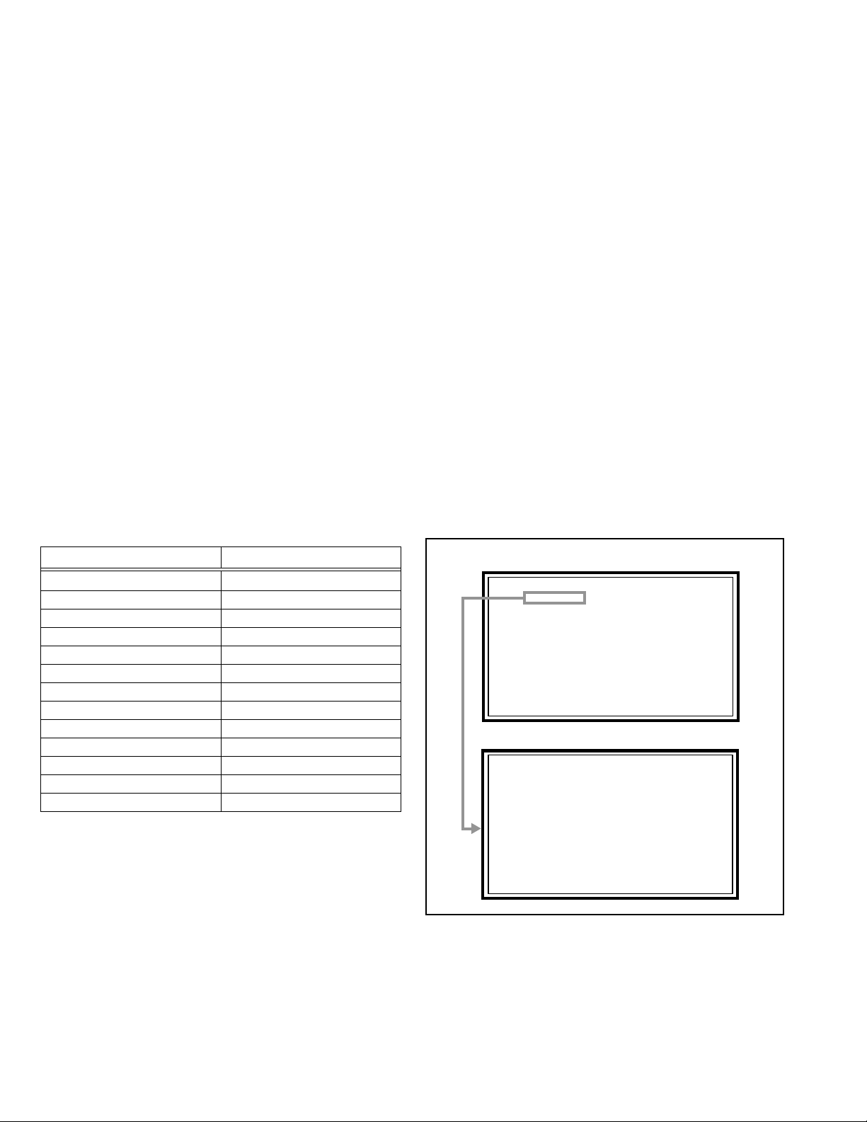
3.3 REPLACEMENT OF MEMORY IC
SERVICE MENU SCREEN
ADJUST MODE SCREEN
3.3.1 MEMORY IC
This unit uses the nonvolatile memory IC.
The memory IC memories data for video and deflection circuits. To replace the memory IC without the data written, malfunctions
might occurred while power is on, and the normal image might not appear. When replacing the memory IC, be sure to use the IC
written with the initial values of data.
3.3.2 PROCEDURE FOR REPLACING THE MEMORY IC
1. Power off
Switch the power off and unplug the power cord from the
SERVICE MENU SCREEN
wall outlet.
2. Replacing the memory IC
Replace the memory IC with new one. Be sure to use the
memory IC written with the initial data values.
SERVICE MENU
1. ADJUST
2. SELF_CHECK
3. I2C STOP
3. Power on
Plug the power cord into the wall outlet and switch the
power on.
4. Receive channel setting
Refer to the OPERATING INSTRUCTIONS and set the
receive channels (channels preset).
5. User setting
ADJUST MODE SCREEN
Check the user setting values in Table 1 to Table 3. If
setting value is different, set the correct value.
For setting, refer to the OPERATING INSTRUCTIONS.
6. Setting of SERVICE MENU
Verify the setting for each setting item in the SERVICE
S001 PREPATE 0
PAL50 FULL STD M
MENU.(See Table 4.) If readjustment is necessary,
perform adjustment referring to “ADJUSTMENTS
PROCEDURE”.
3.3.3 FACTORY SETTING VALUE
3.3.3.1 SETTING OF SWITCHS ON FRONT SIDE OF MAIN BODY
Setting item Setting value
POWER OFF
CHANNEL PR1
VOLUME 10
INPUT TV
Table 1
3.3.3.2 SETTING OF REMOTE CONTROL UNIT
Setting item Setting value
ZOOM PANORAMIC
MULTI PICTURE 1 SCREEN
CINEMA SURROUND OFF
Table 2
Fig.1
(No.YA101) 1-25
Page 26
3.3.3.3 SETTING OF MENU SCREEN
Setting item Setting value
PICTURE SETTING
PICTURE MODE BRIGHT
CONTRAST +6
BRIGHT 0
SHARP +5
COLOUR +3
TINT 0
WHITE BALANCE MID
PICTURE FEATURES
DIGITAL VNR MIN
Super DigiPure AUTO
PULL DOWN AUTO
COLOUR MANAGEMENT ON
PICTURE MANAGEMENT ON
COLOUR SYSTEM MAIN : AUTO
SUB: AUTO
4:3 AUTO ASPECT PANO RAMIC
SOUND SETTING
STEREO / I•II Stereo sound
BASS Center
TREBLE Center
BALANCE Center
CINEMA SURROUND OFF
A.H.B. OFF
BBE OFF
SPEAKER TV
Setting item Setting value
FEATURES
SLEEP TIMER OFF
APPEARANCE TYPE A
BLUE BACK ON
CHILD LOCK OFF
AUTO SHUT OFF OFF
REFRESH OFF
SET UP
EDIT Only for PR / CH
LANGUAGE ENGLISH
VIDEO-1 SETTING COMPONENT
VIDEO-3 SETTING COMPONENT
AI VOLUME ON
TELETEXT LANGUAGE GROUP-1
PICTURE SHIFT FAST
Table 3
3.3.3.4 SERVICE MENU SETTING ITEMS
Service menu Setting item
1. ADJUST
2. SELF CHECK
3. I2C STOP
CAUTION
When a number key other than the [1] to [3] key is pressed in the SERVICE MENU screen, the other relevant screen may be displayed.
This is not used in the adjustment procedure.
Press the [MENU] key to return to the SERVICE MENU.
S001 ~ S039
T001 ~ T010
P001 ~ P010
D001 ~ D187
Z001 ~ Z010
[Refer to “SECTION 5
TROUBLESHOOTING” (page 1-40)]
[Do not adjust]
Table 4
1-26 (No.YA101)
Page 27
3.4 REPLACEMENT OF CHIP COMPONENT
A
B
C
3.4.1 CAUTIONS
(1) Avoid heating for more than 3 seconds.
(2) Do not rub the electrodes and the resist parts of the pattern.
(3) When removing a chip part, melt the solder adequately.
(4) Do not reuse a chip part after removing it.
3.4.2 SOLDERING IRON
(1) Use a high insulation soldering iron with a thin pointed end of it.
(2) A 30w soldering iron is recommended for easily removing parts.
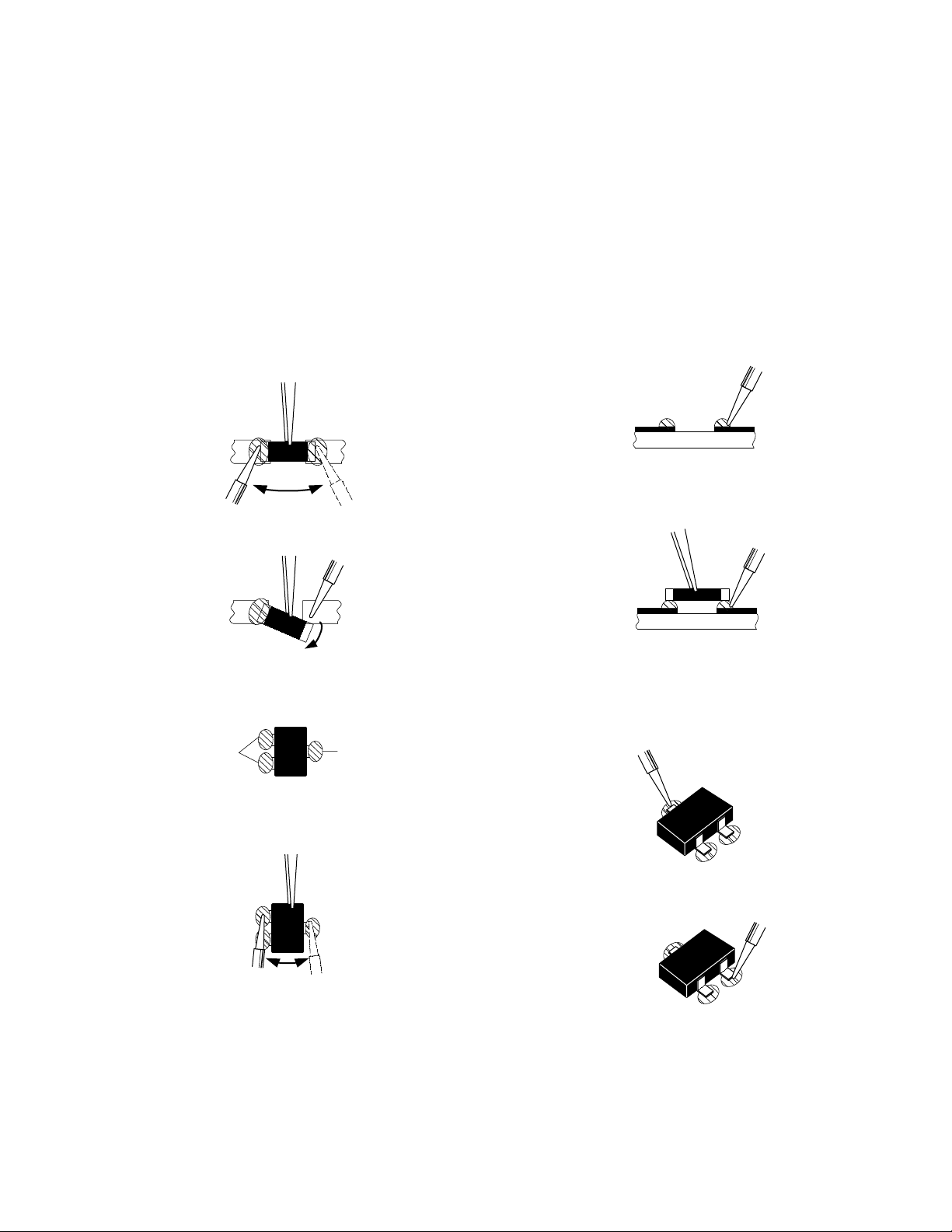
3.4.3 REPLACEMENT STEPS
1. How to remove Chip parts
[Resistors, capacitors, etc.]
(1) As shown in the figure, push the part with tweezers and
alternately melt the solder at each end.
(2) Shift with tweezers and remove the chip part.
2. How to install Chip parts
[Resistors, capacitors, etc.]
(1) Apply solder to the pattern as indicated in the figure.
(2) Grasp the chip part with tweezers and place it on the
solder. Then heat and melt the solder at both ends of
the chip part.
[Transistors, diodes, variable resistors, etc.]
(1) Apply extra solder to each lead.
SOLDER
SOLDER
(2) As shown in the figure, push the part with tweezers and
alternately melt the solder at each lead. Shift and remove
the chip part.
Note :
After removing the part, remove remaining solder from
the pattern.
[Transistors, diodes, variable resistors, etc.]
(1) Apply solder to the pattern as indicated in the figure.
(2) Grasp the chip part with tweezers and place it on the
solder.
(3) First solder lead A as indicated in the figure.
(4) Then solder leads B and C.
A
B
C
(No.YA101) 1-27
Page 28
SECTION 4
SERVICE MENU SCREEN
ADJUST SCREEN
ADJUSTMENT
4.1 ADJUSTMENT PREPARATION
(1) You can make the necessary adjustments for this unit
with either the remote control unit or with the adjustment
equipment and parts as given below.
(2) Adjustment with the remote control unit is made on the
basis of the initial setting values, however, the new
setting values which set the screen to its optimum
condition may differ from the initial settings.
(3) Make sure that AC power is turned on correctly.
(4) Turn on the power for the set and test equipment before
use, and start the adjustment procedures after waiting at
least 30 minutes.
(5) Unless otherwise specified, prepare the most suitable
reception or input signal for adjustment.
(6) Never touch any adjustment parts, which are not specified
in the list for this variable resistors, transformers, trimmer
capacitors, etc.
(7) Presetting before adjustment.
Unless otherwise specified in the adjustment instructions,
preset the following functions with the remote control unit.
4. 2 PRESETTING BEFORE ADJUSTMENT
Unless otherwise specified in the adjustment instructions,
preset the following functions with the remote control unit.
4.4 BASIC OPERATION OF THE SERVICE MENU
4.4.1 TOOL OF SERVICE MENU OPERATION
Operate the SERVICE MENU with the remote control unit.
4.4.2 HOW TO ENTER THE SERVICE MENU
(1) Press the [DISPLAY] key and the [MUTING] key
simultaneously, and the SERVICE MENU screen of Fig.1
will be displayed.
4.4.3 SELECT THE SERVICE MENU ITEM
(1) When the Main Menu is displayed, press any key of the [1]
to [3] key to enter the corresponding menu mode.
CAUTION:
When a number key other than the [1] to [3] key is
pressed in the SERVICE MENU screen, the other
relevant screen may be displayed.
This is not used in the adjustment procedure.
Press the [MENU] key to return to the SERVICE MENU.
4.4.4 SELECT THE SETTING ITEM AND SETTING VALUE
(1) Select the service item using the [FUNCTION (/)] key.
(2) Set the value using the [FUNCTION (
(3) Press the [MUTING] key to memorize the set value.
/)] key.
Setting item Settings
PICTURE MODE STANDARD
PICTURE adjustments All center (00)
WHITE BALANCE MID
DIGITAL VNR MIN
Super DigiPure AUTO
PULL DOWN AUTO
COLOUR MANAGEMENT ON
PICTURE MANAGEMENT ON
SOUND adjustments All center (00)
CINEMA SURROUND OFF
A.H.B OFF
BBE OFF
ZOOM FULL
4.3 MEASURING INSTRUMENT AND FIXTURES
• DC voltmeter (or Digital voltmeter)
• Signal generator (Pattern generator)
[PAL / SECAM / NTSC /625i COMPONENT / 1125i / PC (VGA)]
• Remote control unit
SERVICE MENU SCREEN
SERVICE MENU
1. ADJUST
2. SELF_CHECK
3. I2C STOP
ADJUST SCREEN
S001 PREPATE 0
PAL50 FULL STD M
Fig.1
4.4.5 HOW TO EXIT THE SERVICE MENU MODE
Press the [MENU] key to exit the Service Menu mode.
1-28 (No.YA101)
Page 29
4.4.6 SERVICE CONTROL KEY LAYOUT ON THE REMOTE
CONTROL UNIT
MUTING
1~3
MENU
FUNCTION /
DISPLAY
FUNCTION /
Fig.2
4.4.7 SETTING OF THE SERVICE MENUS
4.4.7.1 [1.ADJUST]
[Do not change setting values of items that are not included in
the “ADJUSTMENT PROCEDURE”. They are fixed values]
Set output data of the port of the video, audio, panel control, drive
and main CPU setting.
(1 ) SIGNAL
The signal displayed on the screen is displayed.
PAL50 : PAL50Hz (Composite / S-video)
PAL60 : PAL60Hz (Composite / S-video)
SECAM : SECAM
NTSC3 : NTSC3.58
NTSC4 : NTSC4.43
525I : 525i (Component)
525P : 525p
625I : 625i (Component)
625P : 625p
750P : 750p
1125I5 : 1125i 50Hz
1125I6 : 1125i 60Hz
PCVGA : PC (VGA)
(2) SCREEN SIZE / MULTI PICTURE
State of the SCREEN SIZE or MULTI PICTURE is displayed.
• SCREEN SIZE
FULL : FULL
PANO : PANORAMIC
1609 : 16:9 ZOOM
1609S : 16:9 ZOOM SUBTITLE
1409 : 14:9 ZOOM
REGU : REGULAR
• MULTI PICTURE
M2 : 2 pictures
M12 : 12 pictures
(3) PICTURE MODE
The PICTURE MODE is displayed.
STD : STANDARD
BRI : BRIGHT
SOFT : SOFT
GAME : GAME
(4) WHITE BALANCE
The WHITE BALANCE is displayed.
H : WARM
M : MID
L : COOL
(5) ITEM No.
The ITEM No. is displayed.
• [Function (/)] key
For scrolling up / down the setting items.
→→
→ S001...
→→
↔↔
↔ T001...
↔↔
↔↔
↔ P001...
↔↔
↔↔
↔ D001...
↔↔
↔↔
↔ Z001...
↔↔
←←
←
←←
(6) SETTING VALUE
The SETTING VALUE is displayed.
• [Function (/)] key
For scrolling up / down the setting values.
Item No. Setting items
S001~S039 This item adjusts the setting values of the video
circuit.
T001~T010 This item adjusts the setting values of the
audio circuit.
P001~P010 This item adjusts the setting values of the
panel control circuit.
D001~D187 This item adjusts the setting values of the drive
circuit.
Z001~Z010 This item adjusts the setting values of the main
CPU circuit.
4.4.7.2 [2.SELF CHECK]
[Refer to “SECTION 5 TROUBLESHOOTING” (page 1-40)]
4.4.7.3 [3.I2C STOP]
[Setting for this item is not required in servicing]
(5) ITEM NO.
S001 PREPATE 0
PAL50 FULL STD M
(1) SIGNAL (3) PICTURE MODE
(2) SCREEN SIZE / MULTI PICTURE
(6) SETTING VALUE
(4) WHITE BALANCE
Fig.3
(No.YA101) 1-29
Page 30
4.5 INITIAL SETTING VALUES IN THE SERVICE MENU SETTING MODE
• Perform fine-tuning based on the “initial setting values” using the remote control when in the SERVICE MENU setting mode.
• The “initial setting values” serve only as an indication rough standard and therefore the values with which optimal display can be
achieved may be different from the initial setting values. But, don't change the values that are not written in “ADJUSTMENT
PROCEDURE”. They are fixed values.
4.5.1 [1.ADJUST]
4.5.1.1 VIDEO SYSTEM
Item No. Item
S001 PREPARE 0~31 0 0 0
S002 NTSC BL 0~15 0 0 0
S003 NTSC CNT 0~255 39 39 39
S004 NT CR OF 0~15 7 7 7
S005 NT CB OF 0~15 7 7 7
S006 525i BL 0~15 0 0 0
S007 525i CNT 0~255 39 39 39
S008 5i CB OF 0~15 0 0 0
S009 5i CR OF 0~15 0 0 0
S010 5i CR GN 0~15 7 7 7
S011 5i CB GN 0~15 7 7 7
S012 HD BL 0~63 56 56 56
S013 HD CB OF 0~63 54 54 54
S014 HD CR OF 0~63 53 53 53
S015 RT CONT 0~15 7 7 7
S016 RT CB OF 0~15 8 8 8
S017 RT CR OF 0~15 8 8 8
S018 RT CL GA 0~15 4 4 4
S019 PC CL MB 0~7 0 0 0
S020 PC CL LB 0~31 0 0 0
S021 PC CL MR 0~7 0 0 0
S022 PC CL LR 0~31 0 0 0
S023 (NO DISPLAY) 0~255 0 0 0
S024 (NO DISPLAY) 0~255 0 0 0
S025 (NO DISPLAY) 0~255 0 0 0
S026 (NO DISPLAY) 0~255 0 0 0
S027 (NO DISPLAY) 0~255 0 0 0
S028 (NO DISPLAY) 0~255 0 0 0
S029 (NO DISPLAY) 0~255 0 0 0
S030 R DRIVE 0~255 133 133 133
S031 G DRIVE 0~255 119 119 119
S032 B DRIVE 0~255 123 123 123
S033 (NO DISPLAY) 0~255 0 0 0
S034 (NO DISPLAY) 0~255 0 0 0
S035 (NO DISPLAY) 0~255 0 0 0
S036 (NO DISPLAY) 0~255 0 0 0
S037 (NO DISPLAY) 0~255 0 0 0
S038 (NO DISPLAY) 0~255 0 0 0
S039 ILA COM 0~1 0 0 0
Variable range
PAL SECAM NTSC
Setting value
4.5.1.2 AUDIO SYSTEM
Item No. Item
T001 IN LEVEL 0~255 0 0 0
T002 LOW SEP 0~255 0 0 0
T003 HIGH SEP 0~255 0 0 0
T004 AFC 0~255 4 4 4
T005 (NO DISPLAY) 0~255 0 0 0
T006 ATT V ON 0~1 1 1 1
T007 ATT U ON 0~1 1 1 1
T008 ATT C ON 0~1 1 1 1
T009 (NO DISPLAY) 0~255 0 0 0
T010 (NO DISPLAY) 0~255 0 0 0
1-30 (No.YA101)
Variable range
PAL SECAM NTSC
Setting value
Page 31

4.5.1.3 PANEL CONTROL SYSTEM
Item No. Item
P001 TM HOR H 0~FF 00 00 00
P002 TM HOR L 0~FF 0 1 02 02
P003 TM MIN 0~FF 16 05 05
P004 TEMP 0~255 57 43 41
P005 (NO DISPLAY) 0~255 0 0 0
P006 (NO DISPLAY) 0~255 0 0 0
P007 (NO DISPLAY) 0~255 0 0 0
P008 (NO DISPLAY) 0~255 0 0 0
P009 (NO DISPLAY) 0~255 0 0 0
P010 (NO DISPLAY) 0~255 0 0 0
4.5.1.4 DRIVE SYSTEM
Item No. Item
D001 SLV GN 0~3F 20 20 20
D002 SLVH GN 0~3F 20 20 20
D003 SLH GN 0~3F 20 20 20
D004 SLV Pf 0~03 01 01 01
D005 SLH Pf H 0~01 01 01 01
D006 SLH Pf L 0~03 01 01 01
D007 SL EGCON 0~3F 07 07 07
D008 SL EGONF 0~01 01 01 01
D009 SL CRGON 0~3F 0 4 04 04
D010 SL CRGON 0~01 01 01 01
D011 SL ON OF 0~01 01 01 01
D012 SV GN 0~3F 10 10 1 7
D013 SVH GN 0~3F 10 10 15
D014 SH GN 0~3F 26 26 2 6
D015 SV Pf 0~03 01 01 01
D016 SV Pf H 0~01 01 01 01
D017 SV Pf L 0~03 02 02 01
D018 SYL CON 0~3F 25 25 25
D019 SYL CONF 0~01 01 01 01
D020 SYH CON 0~3F 22 22 22
D021 SYH CONF 0~01 01 01 01
D022 SC CON 0~3F 33 33 33
D023 SC CNONF 0~01 01 01 01
D024 SPM BLC 0~3F 08 08 08
D025 SPM BLCO 0~01 01 01 01
D026 SLIM 0~3F 30 30 30
D027 SLIMONF 0~01 01 01 01
D028 SCRG 0~3F 03 03 03
D029 SRGONF 0~01 01 01 01
D030 S ONF 0~01 01 01 01
D031 pb GN 0~3F 1F 1F 1F
D032 pb Pf H 0~01 00 00 00
D033 pb Pf L 0~03 03 03 03
D034 pb CRG 0~3F 03 03 03
D035 pb CRGON 0~01 01 01 01
D036 pb ONF 0~01 01 01 01
D037 pr GN 0~3F 1F 1F 1F
D038 pr Pf H 0~01 00 00 00
D039 pr Pf L 0~03 03 03 03
D040 pr CRG 0~3F 03 03 03
D041 pr CRGON 0~01 01 01 01
Variable range
Variable range
PAL SECAM NTSC
PAL SECAM NTSC
Setting value
Setting value
(No.YA101) 1-31
Page 32

Item No. Item
D042 pr ONF 0~01 01 01 01
D043 ENH ONF 0~01 01 01 01
D044 (NO DISPLAY) 0~FF 00 00 00
D045 (NO DISPLAY) 0~FF 00 00 00
D046 (NO DISPLAY) 0~FF 00 00 00
D047 (NO DISPLAY) 0~FF 00 00 00
D048 (NO DISPLAY) 0~FF 00 00 00
D049 (NO DISPLAY) 0~FF 00 00 00
D050 (NO DISPLAY) 0~FF 00 00 00
D051 (NO DISPLAY) 0~FF 00 00 00
D052 (NO DISPLAY) 0~FF 00 00 00
D053 (NO DISPLAY) 0~FF 00 00 00
D054 (NO DISPLAY) 0~FF 00 00 00
D055 (NO DISPLAY) 0~FF 00 00 00
D056 (NO DISPLAY) 0~FF 00 00 00
D057 (NO DISPLAY) 0~FF 00 00 00
D058 (NO DISPLAY) 0~FF 00 00 00
D059 (NO DISPLAY) 0~FF 00 00 00
D060 (NO DISPLAY) 0~FF 00 00 00
D061 (NO DISPLAY) 0~FF 00 00 00
D062 (NO DISPLAY) 0~FF 00 00 00
D063 (NO DISPLAY) 0~FF 00 00 00
D064 (NO DISPLAY) 0~FF 00 00 00
D065 (NO DISPLAY) 0~FF 00 00 00
D066 (NO DISPLAY) 0~FF 00 00 00
D067 (NO DISPLAY) 0~FF 00 00 00
D068 (NO DISPLAY) 0~FF 00 00 00
D069 (NO DISPLAY) 0~FF 00 00 00
D070 (NO DISPLAY) 0~FF 00 00 00
D071 (NO DISPLAY) 0~FF 00 00 00
D072 (NO DISPLAY) 0~FF 00 00 00
D073 (NO DISPLAY) 0~FF 00 00 00
D074 (NO DISPLAY) 0~FF 00 00 00
D075 (NO DISPLAY) 0~FF 00 00 00
D076 (NO DISPLAY) 0~FF 00 00 00
D077 (NO DISPLAY) 0~FF 00 00 00
D078 (NO DISPLAY) 0~FF 00 00 00
D079 (NO DISPLAY) 0~FF 00 00 00
D080 (NO DISPLAY) 0~FF 00 00 00
D081 (NO DISPLAY) 0~FF 00 00 00
D082 (NO DISPLAY) 0~FF 00 00 00
D083 (NO DISPLAY) 0~FF 00 00 00
D084 (NO DISPLAY) 0~FF 00 00 00
D085 (NO DISPLAY) 0~FF 00 00 00
D086 (NO DISPLAY) 0~FF 00 00 00
D087 (NO DISPLAY) 0~FF 00 00 00
D088 (NO DISPLAY) 0~FF 00 00 00
D089 (NO DISPLAY) 0~FF 00 00 00
D090 (NO DISPLAY) 0~FF 00 00 00
D091 (NO DISPLAY) 0~FF 00 00 00
D092 (NO DISPLAY) 0~FF 00 00 00
D093 (NO DISPLAY) 0~FF 00 00 00
D094 (NO DISPLAY) 0~FF 00 00 00
D095 (NO DISPLAY) 0~FF 00 00 00
D096 (NO DISPLAY) 0~FF 00 00 00
Variable range
PAL SECAM NTSC
Setting value
1-32 (No.YA101)
Page 33

Item No. Item
D097 (NO DISPLAY) 0~FF 00 00 00
D098 (NO DISPLAY) 0~FF 00 00 00
D099 (NO DISPLAY) 0~FF 00 00 00
D100 (NO DISPLAY) 0~FF 00 00 00
D101 (NO DISPLAY) 0~FF 00 00 00
D102 (NO DISPLAY) 0~FF 00 00 00
D103 (NO DISPLAY) 0~FF 00 00 00
D104 (NO DISPLAY) 0~FF 00 00 00
D105 (NO DISPLAY) 0~FF 00 00 00
D106 (NO DISPLAY) 0~FF 00 00 00
D107 (NO DISPLAY) 0~FF 00 00 00
D108 (NO DISPLAY) 0~FF 00 00 00
D109 (NO DISPLAY) 0~FF 00 00 00
D110 (NO DISPLAY) 0~FF 00 00 00
D111 (NO DISPLAY) 0~FF 00 00 00
D112 (NO DISPLAY) 0~FF 00 00 00
D113 (NO DISPLAY) 0~FF 00 00 00
D114 (NO DISPLAY) 0~FF 00 00 00
D115 (NO DISPLAY) 0~FF 00 00 00
D116 (NO DISPLAY) 0~FF 00 00 00
D117 (NO DISPLAY) 0~FF 00 00 00
D118 (NO DISPLAY) 0~FF 00 00 00
D119 (NO DISPLAY) 0~FF 00 00 00
D120 (NO DISPLAY) 0~FF 00 00 00
D121 (NO DISPLAY) 0~FF 00 00 00
D122 (NO DISPLAY) 0~FF 00 00 00
D123 (NO DISPLAY) 0~FF 00 00 00
D124 (NO DISPLAY) 0~FF 00 00 00
D125 (NO DISPLAY) 0~FF 00 00 00
D126 (NO DISPLAY) 0~FF 00 00 00
D127 (NO DISPLAY) 0~FF 00 00 00
D128 (NO DISPLAY) 0~FF 00 00 00
D129 (NO DISPLAY) 0~FF 00 00 00
D130 (NO DISPLAY) 0~FF 00 00 00
D131 (NO DISPLAY) 0~FF 00 00 00
D132 (NO DISPLAY) 0~FF 00 00 00
D133 (NO DISPLAY) 0~FF 00 00 00
D134 (NO DISPLAY) 0~FF 00 00 00
D135 (NO DISPLAY) 0~FF 00 00 00
D136 (NO DISPLAY) 0~FF 00 00 00
D137 (NO DISPLAY) 0~FF 00 00 00
D138 (NO DISPLAY) 0~FF 00 00 00
D139 (NO DISPLAY) 0~FF 00 00 00
D140 (NO DISPLAY) 0~FF 00 00 00
D141 (NO DISPLAY) 0~FF 00 00 00
D142 (NO DISPLAY) 0~FF 00 00 00
D143 (NO DISPLAY) 0~FF 00 00 00
D144 (NO DISPLAY) 0~FF 00 00 00
D145 (NO DISPLAY) 0~FF 00 00 00
D146 (NO DISPLAY) 0~FF 00 00 00
D147 (NO DISPLAY) 0~FF 00 00 00
D148 (NO DISPLAY) 0~FF 00 00 00
D149 (NO DISPLAY) 0~FF 00 00 00
D150 (NO DISPLAY) 0~FF 00 00 00
Variable range
PAL SECAM NTSC
Setting value
(No.YA101) 1-33
Page 34

Item No. Item
D151 (NO DISPLAY) 0~FF 00 00 00
D152 (NO DISPLAY) 0~FF 00 00 00
D153 (NO DISPLAY) 0~FF 00 00 00
D154 (NO DISPLAY) 0~FF 00 00 00
D155 (NO DISPLAY) 0~FF 00 00 00
D156 (NO DISPLAY) 0~FF 00 00 00
D157 (NO DISPLAY) 0~FF 00 00 00
D158 (NO DISPLAY) 0~FF 00 00 00
D159 (NO DISPLAY) 0~FF 00 00 00
D160 (NO DISPLAY) 0~FF 00 00 00
D161 (NO DISPLAY) 0~FF 00 00 00
D162 (NO DISPLAY) 0~FF 00 00 00
D163 (NO DISPLAY) 0~FF 00 00 00
D164 (NO DISPLAY) 0~FF 00 00 00
D165 (NO DISPLAY) 0~FF 00 00 00
D166 (NO DISPLAY) 0~FF 00 00 00
D167 (NO DISPLAY) 0~FF 00 00 00
D168 (NO DISPLAY) 0~FF 00 00 00
D169 (NO DISPLAY) 0~FF 00 00 00
D170 (NO DISPLAY) 0~FF 00 00 00
D171 (NO DISPLAY) 0~FF 00 00 00
D172 (NO DISPLAY) 0~FF 00 00 00
D173 (NO DISPLAY) 0~FF 00 00 00
D174 (NO DISPLAY) 0~FF 00 00 00
D175 (NO DISPLAY) 0~FF 00 00 00
D176 (NO DISPLAY) 0~FF 00 00 00
D177 (NO DISPLAY) 0~FF 00 00 00
D178 (NO DISPLAY) 0~FF 00 00 00
D179 (NO DISPLAY) 0~FF 00 00 00
D180 (NO DISPLAY) 0~FF 00 00 00
D181 (NO DISPLAY) 0~FF 00 00 00
D182 (NO DISPLAY) 0~FF 00 00 00
D183 (NO DISPLAY) 0~FF 00 00 00
D184 (NO DISPLAY) 0~FF 00 00 00
D185 (NO DISPLAY) 0~FF 00 00 00
D186 (NO DISPLAY) 0~FF 00 00 00
D187 (NO DISPLAY) 0~FF 00 00 00
Variable range
PAL SECAM NTSC
Setting value
4.5.1.5 MAIN CPU SETTING
Item No. Item
Z001 (NO DISPLAY) 0~0F 00 00 00
Z002 (NO DISPLAY) 0~0F 00 00 00
Z003 (NO DISPLAY) 0~0F 00 00 00
Z004 (NO DISPLAY) 0~FF 00 00 00
Z005 (NO DISPLAY) 0~FF 00 00 00
Z006 (NO DISPLAY) 0~FF 00 00 00
Z007 (NO DISPLAY) 0~FF 00 00 00
Z008 (NO DISPLAY) 0~FF 00 00 00
Z009 (NO DISPLAY) 0~FF 00 00 00
Z010 (NO DISPLAY) 0~FF 00 00 00
1-34 (No.YA101)
Variable range
PAL SECAM NTSC
Setting value
Page 35

4.6 ADJUSTMENT PROCEDURE
Item
Measuring
instrument
Test point Adjustment part Description
PDP POWER
VOLTAGE
[42V]
MAIN POWER PWB voltage adjustment point
CN0C4
1 : Vs
2 : Vset
3 : Ve
4 : NC
5 : Va
6 : NC
7 : Vscan
8 : NC
9 : GND
10 : POWER
11 : PANEL POWER
12 : Vs_ON
POWER
PANEL POWER
Vs_ON
MAIN POWER PWB
Signal generator
DC voltmeter
Resistor (1kΩ)
DC power
supply
CN0C4
Vs
1
Vset
2
Ve
3
NC
4
Va
5
NC
6
Vscan
7
NC
GND
Vscan
8
9
10
11
12
Connector
CN0C4
Vs
Vset
Ve
Va
Vscan
[MAIN POWER
PWB]
Ve
Vs
Vset
Vscan
Fig. 1
Va Ve
Vset
SW1
Fig. 2
Vs VR:170V ADJ
(R9424)
Vset VR:160V ADJ
(R9640)
Ve VR:155V ADJ
(R9646)
Va VR:70V ADJ
(R9219)
Vscan VR:-60V ADJ
(R9628)
[MAIN POWER PWB]
Va
Voltage adjustment VR
Vs
3.3V ~ 5.0V
(DC power supply)
1kΩ
(Resistor)
Voltage label
NTSC
Va
XX XX XX XX XX
NTSC/PAL
Ve VsetVsc Vs
CAUTION:
• During adjustment operation of PDP POWER VOLTAGE,
don't touch the heat sink of the MAIN POWER PWB. If you
touch it, electric shock may be caused.
< When MAIN POWER PWB is not replaced >
(1) Connect the DC voltmeter, load resistor (1kΩ), DC
power supply and switch SW1 to the CN0C4 connector
and turn on the main power and switch SW1. (See
Fig.2)
(2) Adjust Vs (170V ADJ) VR, Vset (160V ADJ) VR, Ve (155V
ADJ) VR, Va (70V ADJ) VR and Vscan (-60V ADJ) VR so
that the Vs, Vset, Ve, Va and Vscan voltage coincides
with the values in the voltage label.
(3) Input a PAL all-black signal and check that it coincides
with the values in the voltage label.
(4) Readjust if the adjusted value is different from those
in the voltage label.
NOTE:
• Designed value for the panel is printed on a label on the
upper-right at the back of the PDP. (See Fig.3)
< When MAIN POWER PWB is replaced >
CAUTION:
• Before making adjustments, be sure not to turn on the
power when the CN8002, CN8003, CN8005, CN8006
and CN8008 connectors are connected, as this may
cause the PDP to break down.
(1) Disconnect the CN8002, CN8003, CN8005, CN8006
and CN8008 connectors on the MAIN POWER PWB.
(2) Connect the DC voltmeter, load resistor (1kΩ), DC
power supply and switch SW1 to the CN0C4 connector
and turn on the main power and switch SW1. (See
Fig.2)
(3) Adjust Vs (170V ADJ) VR, Vset (160V ADJ) VR, Ve (155V
ADJ) VR, Va (70V ADJ) VR and Vscan (-60V ADJ) VR so
that the Vs, Vset, Ve, Va and Vscan voltage coincides
with the values in the voltage label.
(4) Turn off the main power and switch SW1, and connect
the CN8002, CN8003, CN8005, CN8006 and CN8008
connectors and turn on the power again.
(5) Input a PAL all-black signal and check that it coincides
with the values in the voltage label.
(6) If the adjusted value is different from those in the
voltage label, fine-tune without unplugging the
connectors.
CAUTION:
• Designated power supply voltage of the panel (Vs, Vset,
Ve, Va, Vscan) varies according to the PDP unit.
• Pay careful attention during adjustment, as any error in
procedure may cause the PDP to break down.
Fig. 3
(No.YA101) 1-35
Page 36

Item
Measuring
instrument
Test point Adjustment part Description
PDP POWER
Signal generator
VOLTAGE
[35V]
DC voltmeter
MAIN POWER UNIT voltage adjustment point
CN0C4
1. Vs
2. NC
3. Va(Vd)
4. NC
5. 5V
6. GND
Vs value Va(Vd) value
( sxxxx / dxxx ) xxx / xxx / xxx
xxx / xxx / xxx / xxx
xx / xx / xx / xx / xx
xxxxxxx
CN0C4
1
Vs
2
NC
3
Va
4
NC
5
5V
6
GND
Voltage label
Connector
CN0C4
Vs
Va(Vd)
[MAIN POWER
UNIT]
Vs
Va(Vd)
Fig. 4
Va
Fig. 5
Vs VR:190V ADJ
(R1551)
Va VR:60V ADJ
(R1451)
[MAIN POWER UNIT]
Voltage adjustment VR
Vs
MAIN POWER UNIT
CAUTION:
• During adjustment operation of PDP POWER VOLTAGE,
don't touch the heat sink of the MAIN POWER UNIT. If
you touch it, electric shock may be caused.
< When MAIN POWER UNIT is not replaced >
(1) Connect the DC voltmeter to the CN0C4 connector
and turn on the power. (See Fig.5)
(2) Adjust Vs (190V ADJ) VR and Va (60V ADJ) VR so that
the Vs and Va voltage coincides with the values in the
voltage label.
(3) Input a PAL all-black signal and check that it coincides
with the values in the voltage label.
(4) Readjust if the adjusted value is different from those
in the voltage label.
NOTE:
• Designed value for the panel is printed on a label on the
upper-left at the back of the PDP. (See Fig.6)
< When MAIN POWER UNIT is replaced >
CAUTION:
• Before making adjustments, be sure not to turn on the
power when the CN8003 and CN8005 connectors are
connected, as this may cause the PDP to break down.
(1) Disconnect the CN8003 and CN8005 connectors on
the MAIN POWER UNIT.
(2) Connect DC voltmeter to the CN0C4 connector and
turn on the power. (See Fig.5)
(3) Adjust Vs (190V ADJ) VR and Va (70V ADJ) VR so that
the Vs and Va voltage coincides with the values in the
voltage label.
(4) Turn off the power, and connect the CN8003 and
CN8005 connectors and turn on the power again.
(5) Input a PAL all-black signal and check that it coincides
with the values in the voltage label.
(6) If the adjusted value is different from those in the
voltage label, fine-tune without unplugging the
connectors.
CAUTION:
• Designated power supply voltage of the panel (Vs, Va)
varies according to the PDP unit.
• Pay careful attention during adjustment, as any error in
procedure may cause the PDP to break down.
1-36 (No.YA101)
Fig. 6
Page 37

Item
Measuring
instrument
Test point Adjustment part Description
625i A-D
OFFSET
Remote control
unit
Signal generator
[1. ADJUST]
S001:PREPARE
(adjustment setting
mode change)
S008:5i CB OF
(625i blue offset)
S009:5i CR OF
(625i red offset)
S030:R DRIVE
(Red drive)
S031:G DRIVE
(Green drive)
S032:B DRIVE
(Blue drive)
(1) Receive a 625i component ramp pattern signal.
(2) Set PICTURE MODE to “STANDARD”.
(3) Select “1.ADFJUST” from the SERVICE MENU.
(4) Set < S030 > (Red drive), < S031 > (Green drive) and
< S032 > (Blue drive) to set “133”.
(5) Set < S001 >(adjustment setting mode change) to set
“008” and it change to the 625i A-D offset adjustment
setting mode.
(6) Set < S008 > (625i blue offset) and < S009 > (625i red
offset) to lose the gap (red line, green line and blue
line) which appears at both ends of a white part at the
center of the screen. (See Fig.7)
(7) Set < S001 > to set “000” and it change to the normal
mode.
(8) Press the [MUTING] key to memorize the set value.
1125i
BRIGHTNESS
Lose the gap (red line, green line and blue line)
which appears at both ends.
Fig. 7
Remote control
unit
[1. ADJUST]
S001:PREPARE
(adjustment setting
Signal generator
mode change)
S012:HD BL
(1125i brightness)
S030:R DRIVE
(Red drive)
S031:G DRIVE
(Green drive)
S032:B DRIVE
(Blue drive)
Set the 0% black part to be brightest.
(1) Receive a 1125i (50 Hz) gray scale pattern signal
(including 0% black signal).
(2) Set PICTURE MODE to “STANDARD”.
(3) Select “1.ADFJUST” from the SERVICE MENU.
(4) Set < S030 > (Red drive), < S031 > (Green drive) and
< S032 > (Blue drive) to set “133”.
(5) Set < S001 > (adjustment setting mode change) to
set the values “012” and it change to the 1125i black
level adjustment setting mode.
(6) Set < S012 > (1125i brightness) to set the 0% black
part in the upper half of the screen to be brightest.
(See Fig.8)
(7) Set < S001 > to set “000” and it change to the normal
mode.
(8) Press the [MUTING] key to memorize the set value.
Fig.8
(No.YA101) 1-37
Page 38

Item
1125i
A-D OFFSET
Measuring
instrument
Test point Adjustment part Description
Remote control
unit
Signal generator
Minimize the red and blue noises
in the upper half of the screen.
[1. ADJUST]
S001:PREPARE
(adjustment setting
mode change)
S013:HD CB OF
(1125i blue offset)
S014:HD CR OF
(1125i res offset)
S030:R DRIVE
(Red drive)
S031:G DRIVE
(Green drive)
S032:B DRIVE
(Blue drive)
(1) Receive a 1125i (50 Hz) 30% all-white pattern signal.
(2) Set PICTURE MODE to “STANDARD”.
(3) Select “1.ADFJUST” from the SERVICE MENU.
(4) Set < S030 > (Red drive), < S031 > (Green drive) and
< S032 > (Blue drive) to set “133”.
(5) Set < S001 > (adjustment setting mode change) to
set “013” and it change to the 1125i A-D offset
adjustment setting mode.
(6) Set < S013 > (1125i blue offset) to minimize the blue
noise in the upper half of the screen. (See Fig.9)
(7) Set < S014 > (1125i red offset) to minimize the red
noise in the upper half of the screen. (See Fig.9)
(8) Readjust < S013 > and < S014 > to set the upper half
of the screen to be the blackest. (See Fig.9)
(9) Set < S001 > to set “000” and it change to the normal
mode.
(10)
Press the [MUTING] key to memorize the set value.
SUB-SCREEN
A-D OFFSET
Minimize the red and blue noisese in the upper half of the the screen.
Remote control
unit
Signal generator
Fig. 9
[1. ADJUST]
S001:PREPARE
(adjustment setting
mode change)
S016:RT CB OF
(Sub screen blue
offset)
S017:RT CR OF
(Sub screen red
offset)
S030:R DRIVE
(Red drice)
S031:G DRIVE
(Green drive)
S032:B DRIVE
(Blue drive)
(1) Set PICTURE MODE to “STANDARD”.
(2) Set MULTI-PICTURE to “TWIN-PICTURE”.
(3) Receive a PAL 30% - all white pattern signal on the
right screen. At this time, make the left screen VIDEO1 mode (No signal).
(4) Select “1.ADFJUST” from the SERVICE MENU.
(5) Set < S030 > (Red drive), < S031 > (Green drive) and
< S032 > (Blue drive) to set “133”.
(6) Set < S001 > (adjustment setting mode change) to
set “017” and it change to the sub-screen A-D offset
adjustment setting mode.
(7) Set < S016 > (Sub-screen blue offset) to minimize the
blue noise in the upper half of the screen. (See Fig.10)
NOTE:
• If you select an adjustment item < S016 >, then the
screen automatically turn to twin pictures mode.
(8) Set < S017 > (Sub-screen red offset) to minimize the
red noise in the upper half of the screen. (See Fig.10)
(9) Readjust < S016 > and < S017 > to set the upper half
of the screen to be the blackest. (See Fig.10)
(10 )
Set < S001 > to set “000” and it change to the normal
mode.
(11)
Press the [MUTING] key to memorize the set value.
1-38 (No.YA101)
VIDEO-1
<NO SIGNAL>
Fig. 10
TV(RF)
<30% all white>
Page 39

Item
Measuring
instrument
Test point Adjustment part Description
WHITE
BALANCE
(HIGH LIGHT)
Remote control
unit
Signal generator
[1. ADJUST]
S030:R DRIVE
(Red drive)
S031:G DRIVE
(Green drive)
S032:B DRIVE
(Blue drive)
(1) Receive a PAL 75% all-white pattern signal.
(2) Set PICTURE MODE to “STANDARD”.
(3) Set COLOUR TEMPERATURE to “NORMAL”.
(4) Select “1.ADFJUST” from the SERVICE MENU.
(5) Keep one of < S030 > (Red drive), < S031 > (Green
drive) or < S032 > (Blue drive) unchanged, then lower
the other two so that the all-white screen is equally
white throughout.
NOTE:
• Set one or more of < S030 >, < S031 > and < S032 > to
set values “133”.
(6) Check that white balance is properly tracked from low
light to high light. If the white balance tracking is
deviated, adjust to correct it.
(7) Press the [MUTING] key to memorize the set value.
(No.YA101) 1-39
Page 40

SECTION 5
SERVICE MENU SCREEN
< SELF-CHECK SCREEN (Page 1) >
< SELF-CHECK SCREEN (Page 2) >
TROUBLESHOOTING
5. 1 SELF-CHECK FEATURE
5.1.1 OUTLINE
This model has a “Self-check function”, which checks the
operation state of the circuits and informs us of a failure by
flashing POWER LED when a failure occurs.
Diagnosis is performed when power is turned on, and
information input to the main microcomputer is monitored at all
time.
Failure detection is based on input state of I
various control lines connected to the main microcomputer.
5.1.2 HOW TO ENTER THE SELF-CHECK MODE
(1) Press the [DISPLAY] key and the [MUTING] key
simultaneously, then the SERVICE MENU screen will be
displayed. (See Fig.1)
(2) In the SERVICE MENU, press the [2] key. Then, the SELF-
CHECK screen will be displayed. (See Fig.2)
(3) Press the [ZOOM (red)] key, then the second page of the
SELF-CHECK screen will be displayed.
NOTE:
2
C bus and the
• When the [CINEMA (green)] key pressed, the first page
and the second page change screen.
SERVICE MENU SCREEN
SERVICE MENU
1. ADJUST
2. SELF CHECK
3. I2C STOP
Fig. 1
< SELF-CHECK SCREEN (Page 1) >
5.1.3 HOW TO EXIT THE SELF-CHECK
(1) When you leave the failure history
Press the [MENU] key to exit the SELF-CHECK.
(2) When you not leave the failure history
In the SELF-CHECK, press the [POWER] key. Then the
power is turned off.
5.1.4 FAILURE HISTORY
Failure history can be counted up to 9 times for each item.When
the number exceeds 9, display will remain as 9. Failure history
will be stored in the memory unless it has been deleted.
NOTE:
Only SYNC (with/without sync signals) will be neither counted
nor stored.
5.1.5 POINTS TO NOTE WHEN USING THE SELF-CHECK
FEATURE
In addition to circuit failures (abnormal operation), the following
cases may also be iagnosed as “Abnormal” and displayed and
counted as “NG”.
(1) Temporary defective transmissions across circuits due
to pulse interruptions.
(2) Misalignment in the on/off timing of power for I
when turning on/off the main power.
Diagnosis may be impeded if a large number of items are
displayed as “NG”. As such, start self-check only after 5 seconds
in the case of panels upon turning on the power. If recurrences
are expected, ensure to clear (reset) the failure history and record
the new self-check reults.
2
C bus (Vcc)
LOB OK FAN OK
SYNC M:OK S:OK HD:OK
TIM OK
MSM OK DIGI OK
MEM OK AVSW OK
YC OK AIO OK
TUN OK GCR OK
IP OK RGB NG 2
DVI OK HDMI OK
Item Item
CHECK
Normality : OK
Abnormality : NG
* As “SYNC” is not counted, the number of failures not displayed.
< SELF-CHECK SCREEN (Page 2) >
FAN OK ALM OK
TMP OK
ATP OK ASH OK
PNL OK MEM OK
TMP OK AIO OK
1-40 (No.YA101)
Fig. 2
Page 41

5.1.6 DETAILS
Self- check is performed for the following items.
< PAGE 1 OF SCREEN >
Detection item
Low bias line short
protection
Item
name
LOB
Detection content
Confirm the operation of the low bais
(2.5V / 3.3V / 5V / 9V) protection circuit.
Q9822 [REGULATOR PWB]
Fan lock
FAN
Not used.
Detection
signal (line)
LB_PRO
---
Detection timing
Detection starts 3 seconds after the power is
turned on.
If error continues between 400ms, the power
is turned off.
Not used.
Presence of sync
signal
AC power input
Main CPU
communication
Digital tuner
Main memory
AV select
3 dimensions YC
separation
Multi sound
process
RF tuner
Ghost reduction
SYNC
TIM
MSM
DIGI
MEM
AVSW
YC
AIO
TUN
GCR
Confirmation of presence of video
sync signal.
M : Main sync signal
S : Sub sync signal
HD : Component sync signal
IC201 [ANALOG SIGNAL PWB]
Not used.
Confirmation of ACK (response)
signal which uses sync
communications with chassis CPU.
IC7501 [DIGITAL SIGNAL PWB]
Not used.
Confirmation of reply of ACK signal
which uses I
2
C communication.
IC7602 [DIGITAL SIGNAL PWB]
Same as above.
IC301, IC501
[ANALOG SIGNAL PWB]
Same as above.
IC1001 [DIGITAL SIGNAL PWB]
Same as above.
IC3501 [RECEIVER PWB]
Same as above.
IC3001 [RECEIVER PWB]
Not used.
SDA
---
WAKE
---
SDA
SDA
SDA
SDA
SDA
---
Confirmation of presence of sync signal in
video signal.
Not used.
If it checks whenever sync communication with
SHM performed , and no reply of ACK signal,
an error will be counted.
Not used.
2
If it checks whenever I
C communication is
performed, and no reply of ACK signal, an error
will be counted.
Same as above.
Same as above.
Same as above.
Same as above.
Not used.
DIST process
RGB process
DVI (Digital
communication)
Digital input
IP
RGB
DVI
HDMI
Confirmation of reply of ACK signal
which uses I
2
C communication.
IC3001 [DIGITAL SIGNAL PWB]
Same as above.
IC4001 [DIGITAL SIGNAL PWB]
Not used.
Not used.
SDA
SDA
---
---
2
If it checks whenever I
C communication is
performed, and no reply of ACK signal, an error
will be counted.
Same as above.
Not used.
Not used.
(No.YA101) 1-41
Page 42

< PAGE 2 OF SCREEN >
Detection item
Fan lock
Item
name
FAN
Not used.
Detection content
Detection
signal (line)
---
Detection timing
Not used.
Abnormal of
operation of PDP
(PANEL)
Abnormal rise of
temperature in PDP
(PANEL)
Abnormal rise of
temperature in
AUDIO PWB
Short circuit detection
of AUDIO PWB
Panel communication
Panel memory
Temp. sensor
operation
Audio control
ALM
TMP
ATP
ASH
PNL
MEM
TMP
AIO
Confirm the operation of the panel
protection.
[PDP UNIT]
It detects whether the temperature in
a display unit is normal.
IC8101 [TEMP. SENSOR PWB]
Not used
Not used.
It confirm whether panel
communication is normal.
[PDP UNIT]
Confirmation of reply of ACK signal
which uses I
2
C communication.
IC805 [INTERFACE PWB]
Same as above.
IC8101 [TEMP. SENSOR PWB]
Same as above.
IC6521 [AUDIO PWB]
SDA
SDA
---
---
SDA
SDA
SDA
SDA
Detection starts 8 seconds after the power is
turned on.
Detection is performed every 16ms.
If errors continues between 300ms, the power
is turned off.
Detection starts 8 seconds after the power is
turned on.
Detection is performed every 0.5 seconds.
If a temperature rises beyond the temperature
°
C for detection of error over the
of 71
predetermined 120 times, the power is turned
off.
Not used
Not used.
2
If it checks whenever I
C communication is
performed, and no reply of ACK signal, an error
will be counted.
If it checks whenever I
2
C communication is
performed, and no reply of ACK signal, an error
will be counted.
Same as above.
Same as above.
5.1.7 METHOD OF DISPLAY WHEN A RASTER IS NOT OUTPUT
In the state where a raster is not output by breakdown of the set, an error is displayed by blink of the POWER LED.
Type of error
Item name
POWER LED flash cycle
Low bias line short LOB Low luminance blue Flash 1.0 second / Low luminance blue Out 1.0 seconds
Abnormal of operation of PDP (PANEL) ALM High luminance blue Flash 1.0 second / High luminance blue Out 1.0 seconds
Abnormal rise of temperature in PDP (PANEL) TMP High luminance blue Flash 2.0 second / High luminance blue Out 2.0 seconds
Abnormal rise of temperature in AUDIO PWB ATP High luminance blue Flash 0.1 second / Low luminance blue Out 0.1 seconds
< EXPLANATION OF OPERATION >
If error is detected, the power is turned off.
Shortly after a power is turned off, POWER LED will be blinked.
Power cannot be turned on until the power cord takes out and inserts, after a power is turned off.
1-42 (No.YA101)
Page 43

Victor Company of Japan, Limited
AV & MULTIMEDIA COMPANY VIDEO DISPLAY CATEGORY 12, 3-chome, Moriya-cho, kanagawa-ku, Yokohama, kanagawa-prefecture, 221-8528, Japan
(No. YA101)
Printed in Japan
WPC
Page 44

PARTS LIST
CAUTION
J The parts identified by the symbol are important for the safety . Whenever replacing these parts, be sure to use specified ones to secure the
safety.
J The parts not indicated in this Parts List and those which are filled with lines --- in the Parts No. columns will not be supplied.
J P.W. BOARD Ass'y will not be supplied, but those which are filled with the Parts No. in the Parts No. columns will be supplied.
ABBREVIATIONS OF RESISTORS, CAPACITORS AND TOLERANCES
RESISTORS CAPACITORS
CR Carbon Resistor C CAP. Ceramic Capacitor
FR Fusible Resistor E CAP. Electrolytic Capacitor
PR Plate Resistor M CAP. Mylar Capacitor
VR Variable Resistor CH CAP. Chip Capacitor
HV R High Voltage Resistor HV CAP. High Voltage Capacitor
MF R Metal Film Resistor MF CAP. Metalized Film Capacitor
MG R Metal Glazed Resistor MM CAP. Metalized Mylar Capacitor
MP R Metal Plate Resistor MP CAP. Metalized Polystyrol Capacitor
OM R Metal Oxide Film Resistor PP CAP. Polypropylene Capacitor
CMF R Coating Metal Film Resistor PS CAP. Polystyrol Capacitor
UNF R Non-Flammable Resistor TF CAP. Thin Film Capacitor
CH V R Chip Variable Resistor MPP CAP. Metalized Polypropylene Capacitor
CH MG R Chip Metal Glazed Resistor TAN. CAP. Tantalum Capacitor
COMP. R Composition Resistor CH C CAP. Chip Ceramic Capacitor
LPTC R Linear Positive Temperature Coefficient Resistor BP E CAP. Bi-Polar Electrolytic Capacitor
CH AL E CAP. Chip Aluminum Electrolytic Capacitor
CH AL BP CAP. Chip Aluminum Bi-Polar Capacitor
CH TAN. E CAP. Chip Tantalum Electrolytic Capacitor
CH AL BP E CAP. Chip Tantalum Bi-Polar Electrolytic Capacitor
RESISTORS
FGJ KMNRHZ P
±1% ±2% ±5% ±10% ±20% ±30%
+30%
-10%
+50%
-10%
+80%
-20%
+100%
-0%
(No.YA101)3-1
Page 45

CONTENTS
PD-Z42DV4, PD-Z42DV4/S
USING P.W. BOARD & REMOTE CONTROL UNIT .................................................................................................. 3-4
EXPLODED VIEW PARTS LIST - 1 ............................................................................................................................ 3-4
EXPLODED VIEW - 1 .................................................................................................................................................. 3-5
EXPLODED VIEW PARTS LIST - 2 ............................................................................................................................ 3-6
EXPLODED VIEW - 2 .................................................................................................................................................. 3-7
EXPLODED VIEW PARTS LIST - 3 ............................................................................................................................ 3-8
EXPLODED VIEW - 3 .................................................................................................................................................. 3-9
EXPLODED VIEW PARTS LIST - 4 .......................................................................................................................... 3-10
EXPLODED VIEW - 4 ................................................................................................................................................ 3-11
PRINTED WIRING BOARD PARTS LIST [PD-Z42DV4] .......................................................................................... 3-12
RECEIVER P.W. BOARD ASS'Y (SFP-0F301A) (LCA10476-01C) ................................................................ 3-12
ANALOG SIGNAL P.W. BOARD ASS'Y (SFP-0A301A) (LCA10423-06B) ..................................................... 3-12
AV JACK P.W. BOARD ASS'Y (SFP-0J301A) (LCA10445-02B) .................................................................... 3-15
DIGITAL SIGNAL P.W. BOARD ASS'Y (SFP-0D301A) (LCA10428-08F) ....................................................... 3-15
INTERFACE P.W. BOARD ASS'Y (SFP-7301A) (LCA10424-06B) ................................................................. 3-21
AUDIO P.W. BOARD ASS'Y (SFP-6003A) (LCA10420-03C) .......................................................................... 3-22
FRONT CONTROL P.W. BOARD ASS'Y (SFP-8201A) (LCA10446-01D) ...................................................... 3-23
FRONT LED P.W. BOARD ASS'Y (SFP-8201A) (LCA10446-01D) ................................................................. 3-24
TEMP. SENSOR P.W. BOARD ASS'Y (SFP-8201A) (LCA10446-01D) .......................................................... 3-24
REGULATOR P.W. BOARD ASS'Y (SFP-9203A) (LCA10426-01B) ............................................................... 3-24
LINE FILTER P.W. BOARD ASS'Y (SFP-9303A) (LCA10427-06A) ................................................................ 3-24
MAIN POWER P.W. BOARD ASS'Y (SFP-9301A) (LCA10453-05B) .............................................................. 3-25
SUB POWER P.W. BOARD ASS'Y (SFP-9104A) (LCA10422-02C) ............................................................... 3-27
X-MAIN P.W. BOARD ASS'Y (LJ92-00943A) .................................................................................................. 3-27
Y-MAIN P.W. BOARD ASS'Y (LJ92-00944B) .................................................................................................. 3-27
E-BUFFER P.W. BOARD ASS'Y (LJ92-00811A) ............................................................................................ 3-27
F-BUFFER P.W. BOARD ASS'Y (LJ92-00812A) ............................................................................................. 3-27
G-BUFFER P.W. BOARD ASS'Y (LJ92-00813A) ............................................................................................ 3-27
LOGIC-MAIN P.W. BOARD ASS'Y (LJ92-00975A) ......................................................................................... 3-28
Y-BUFFER-U P.W. BOARD ASS'Y (LJ9200796A) .......................................................................................... 3-28
Y-BUFFER-L P.W. BOARD ASS'Y (LJ9200797A) .......................................................................................... 3-28
PRINTED WIRING BOARD PARTS LIST [PD-Z42DV4/S] ....................................................................................... 3-29
RECEIVER P.W. BOARD ASS'Y (SFP-0F301A) (LCA10476-01C) ................................................................ 3-29
ANALOG SIGNAL P.W. BOARD ASS'Y (SFP-0A301A) (LCA10423-06B) ..................................................... 3-29
AV JACK P.W. BOARD ASS'Y (SFP-0J301A) (LCA10445-02B) .................................................................... 3-29
DIGITAL SIGNAL P.W. BOARD ASS'Y (SFP-0D302A) (LCA10428-09F) ....................................................... 3-29
INTERFACE P.W. BOARD ASS'Y (SFP-7302A) (LCA10424-07B) ................................................................. 3-34
AUDIO P.W. BOARD ASS'Y (SFP-6003A) (LCA10420-03C) .......................................................................... 3-35
FRONT CONTROL P.W. BOARD ASS'Y (SFP-8201A) (LCA10446-01D) ...................................................... 3-35
FRONT LED P.W. BOARD ASS'Y (SFP-8201A) (LCA10446-01D) ................................................................. 3-35
TEMP. SENSOR P.W. BOARD ASS'Y (SFP-8201A) (LCA10446-01D) .......................................................... 3-35
REGULATOR P.W. BOARD ASS'Y (SFP-9203A) (LCA10426-01B) ............................................................... 3-35
LINE FILTER P.W. BOARD ASS'Y (SFP-9303A) (LCA10427-06A) ................................................................ 3-36
MAIN POWER P.W. BOARD ASS'Y (SFP-9301A) (LCA10453-05B) .............................................................. 3-36
SUB POWER P.W. BOARD ASS'Y (SFP-9104A) (LCA10422-02C) ............................................................... 3-36
X-MAIN P.W. BOARD ASS'Y (LJ92-00943A) .................................................................................................. 3-36
Y-MAIN P.W. BOARD ASS'Y (LJ92-00944B) .................................................................................................. 3-36
E-BUFFER P.W. BOARD ASS'Y (LJ92-00811A) ............................................................................................ 3-36
F-BUFFER P.W. BOARD ASS'Y (LJ92-00812A) ............................................................................................. 3-36
G-BUFFER P.W. BOARD ASS'Y (LJ92-00813A) ............................................................................................ 3-36
LOGIC-MAIN P.W. BOARD ASS'Y (LJ92-00975A) ......................................................................................... 3-36
Y-BUFFER-U P.W. BOARD ASS'Y (LJ9200796A) .......................................................................................... 3-36
Y-BUFFER-L P.W. BOARD ASS'Y (LJ9200797A) .......................................................................................... 3-36
REMOTE CONTROL UNIT PARTS LIST (RM-C1830-1C) ....................................................................................... 3-36
PACKING PARTS LIST ............................................................................................................................................. 3-36
PACKING ................................................................................................................................................................... 3-37
3-2(No.YA101)
Page 46

PD-Z35DV4, PD-Z35DV4/S
USING P.W. BOARD & REMOTE CONTROL UNIT ................................................................................................ 3-38
EXPLODED VIEW PARTS LIST - 1 .......................................................................................................................... 3-38
EXPLODED VIEW - 1 ................................................................................................................................................ 3-39
EXPLODED VIEW PARTS LIST - 2 .......................................................................................................................... 3-40
EXPLODED VIEW - 2 ................................................................................................................................................ 3-41
EXPLODED VIEW PARTS LIST - 3 .......................................................................................................................... 3-42
EXPLODED VIEW - 3 ................................................................................................................................................ 3-43
EXPLODED VIEW PARTS LIST - 4 .......................................................................................................................... 3-44
EXPLODED VIEW - 4 ................................................................................................................................................ 3-45
PRINTED WIRING BOARD PARTS LIST [PD-Z35DV4] .......................................................................................... 3-46
RECEIVER P.W. BOARD ASS'Y (LCA10476-01C) (SFP-0F301A) ................................................................ 3-46
ANALOG SIGNAL P.W. BOARD ASS'Y (LCA10423-06B) (SFP-0A301A) .................................................... 3-46
AV JACK P.W. BOARD ASS'Y (LCA10445-02B) (SFP-0J301A) .................................................................... 3-46
DIGITAL SIGNAL P.W. BOARD ASS'Y (LCA10428-11F) (SFP-0D304A) ...................................................... 3-46
INTERFACE P.W. BOARD ASS'Y (LCA10424-09B) (SFP-7304A) ................................................................. 3-51
AUDIO P.W. BOARD ASS'Y (LCA10420-07C) (SFP-6007A) ......................................................................... 3-52
FRONT CONTROL P.W. BOARD ASS'Y (LCA10446-01D) (SFP-8201A) ...................................................... 3-54
FRONT LED P.W. BOARD ASS'Y (LCA10446-01D) (SFP-8201A) ................................................................ 3-54
TEMP. SENSOR P.W. BOARD ASS'Y (LCA10446-01D) (SFP-8201A) .......................................................... 3-54
REGULATOR P.W. BOARD ASS'Y (LCA10426-01B) (SFP-9203A) ............................................................... 3-54
LINE FILTER P.W. BOARD ASS'Y (LCA10427-06A) (SFP-9303A) ................................................................ 3-54
SUB POWER P.W. BOARD ASS'Y (LCA10422-02C) (SFP-9104A) ............................................................... 3-54
PANEL POWER P.W. BOARD ASS'Y (NE-9S899437) ................................................................................... 3-54
SCANNING DRIVE P.W. BOARD ASS'Y (NE-9S899376) .............................................................................. 3-54
BRIDGE P.W. BOARD ASS'Y (NE-9S899594) ............................................................................................... 3-54
COMMON DRIVE P.W. BOARD ASS'Y (NE-9S899382) ................................................................................ 3-54
SIGNAL DRIVE-L P.W. BOARD ASS'Y (NE-9S899510) ................................................................................. 3-55
SIGNAL DRIVE-R P.W. BOARD ASS'Y (NE-9S899492) ................................................................................ 3-55
LOGIC CONTROL P.W. BOARD ASS'Y (NE-9S899635) ............................................................................... 3-55
PRINTED WIRING BOARD PARTS LIST [PD-Z35DV4/S] ....................................................................................... 3-56
RECEIVER P.W. BOARD ASS'Y (LCA10476-01C) (SFP-0F301A) ................................................................ 3-56
ANALOG SIGNAL P.W. BOARD ASS'Y (LCA10423-06B) (SFP-0A301A) .................................................... 3-56
AV JACK P.W. BOARD ASS'Y (LCA10445-02B) (SFP-0J301A) .................................................................... 3-56
DIGITAL SIGNAL P.W. BOARD ASS'Y (LCA10428-12F) (SFP-0D305A) ...................................................... 3-56
INTERFACE P.W. BOARD ASS'Y (LCA10424-10B) (SFP-7305A) ................................................................. 3-61
AUDIO P.W. BOARD ASS'Y (LCA10420-07C) (SFP-6007A) ......................................................................... 3-62
FRONT CONTROL P.W. BOARD ASS'Y (LCA10446-01D) (SFP-8201A) ...................................................... 3-62
FRONT LED P.W. BOARD ASS'Y (LCA10446-01D) (SFP-8201A) ................................................................ 3-63
TEMP. SENSOR P.W. BOARD ASS'Y (LCA10446-01D) (SFP-8201A) .......................................................... 3-63
REGULATOR P.W. BOARD ASS'Y (LCA10426-01B) (SFP-9203A) ............................................................... 3-63
LINE FILTER P.W. BOARD ASS'Y (LCA10427-06A) (SFP-9303A) ................................................................ 3-63
SUB POWER P.W. BOARD ASS'Y (LCA10422-02C) (SFP-9104A) ............................................................... 3-63
PANEL POWER P.W. BOARD ASS'Y (NE-9S899437) ................................................................................... 3-63
SCANNING DRIVE P.W. BOARD ASS'Y (NE-9S899376) .............................................................................. 3-63
BRIDGE P.W. BOARD ASS'Y (NE-9S899594) ............................................................................................... 3-63
COMMON DRIVE P.W. BOARD ASS'Y (NE-9S899382) ................................................................................ 3-63
SIGNAL DRIVE-L P.W. BOARD ASS'Y (NE-9S899510) ................................................................................. 3-63
SIGNAL DRIVE-R P.W. BOARD ASS'Y (NE-9S899492) ................................................................................ 3-63
LOGIC CONTROL P.W. BOARD ASS'Y (NE-9S899635) ............................................................................... 3-63
REMOTE CONTROL UNIT PARTS LIST (RM-C1830-1C) ....................................................................................... 3-64
PACKING PARTS LIST ............................................................................................................................................. 3-64
PACKING ................................................................................................................................................................... 3-65
(No.YA101)3-3
Page 47

USING P.W. BOARD & REMOTE CONTROL UNIT
[PD-Z42DV4, PD-Z42DV4/S]
P.W.B ASS'Y PD-Z42DV4 PD-Z42DV4/S
RECEIVER P.W.B SFP-0F301A (LCA10476-01C)
ANALOG SIGNAL P.W.B SFP-0A301A (LCA10423-06B)
AV JACK P.W.B SFP-0J301A (LCA10445-02B)
DIGITAL SIGNAL P.W.B SFP-0D301A (LCA10428-08F) SFP-0D302A (LCA10428-09F)
INTERFACE P.W.B SFP-7301A (LCA10424-06B) SFP-7302A (LCA10424-07B)
AUDIO P.W.B SFP-6003A (LCA10420-03C)
FRONT CONTROL P.W.B SFP-8201A (LCA10446-01D)
FRONT LED P.W.B SFP-8201A (LCA10446-01D)
TEMP. SENSOR P.W.B SFP-8201A (LCA10446-01D)
REGULATOR P.W.B SFP-9203A (LCA10426-01B)
LINE FILTER P.W.B SFP-9303A (LCA10427-06A)
MAIN POWER P.W.B SFP-9301A (LCA10453-05B)
SUB POWER P.W.B SFP-9104A (LCA10422-02C)
PDP UNIT
X-MAIN P.W.B LJ92-00943A
Y-MAIN P.W.B LJ92-00944B
E-BUFFER P.W.B LJ92-00811A
F-BUFFER P.W.B LJ92-00812A
G-BUFFER P.W.B LJ92-00813A
LOGIC-MAIN P.W.B LJ92-00975A
Y-BUFFER-U P.W.B LJ9200796A
Y-BUFFER-L P.W.B LJ9200797A
REMOTE CONTROL UNIT RM-C1830-1C
←
←
←
←
←
←
←
←
←
←
←
←
←
←
←
←
←
←
←
←
EXPLODED VIEW PARTS LIST - 1
Ref.No. Part No. Part Name Description Local
1 LC41647-001B SCREW (x15)
2 QYSBSFG4016MA TAP SCREW M4 x 16mm(x4)
3 QYSBSG3008MA TAP SCREW M3 x 8mm(x8)
4 LC11892-001B-0K REAR COVER
5 QYSBSG3008MA TAP SCREW M3 x 8mm(x6)
6 QYSBSF3008MA TAP SCREW M3 x 8mm(x12)
7 QYSBSG3012MA TAP SCREW M3 x 12mm
8 CE42112-002 PALJ CONNECTOR
9 WJX0006-003A E-COAXIAL ASS'Y
10 LC11933-003C-0K TERMINAL COVER
11 QYSBSG3008MA TAP SCREW M3 x 8mm(x6)
12 LC11893-001A-0K CENTER COVER
13 LC41693-001A CAUTION LABEL
14 LC21716-001A-0L RATING LABEL
15 LC32822-003A TERMINAL LABEL
16 LC41694-001A INLET LABEL
3-4(No.YA101)
Page 48

EXPLODED VIEW - 1
13
1
1
14
3
2
16
15
2
11
12
CHASSIS
SHIELD
COVER
4
5
6
9
8
5
10
8
7
5
TOP
(No.YA101)3-5
Page 49

EXPLODED VIEW PARTS LIST - 2
Ref.No. Part No. Part Name Description Local
20 QYSBSG3012MA TAP SCREW M3 x 12mm
21 QYSBSG3008MA TAP SCREW M3 x 8mm
22 LC21553-001C-0K AC INLET PANEL
23 QYSBSG3008MA TAP SCREW M3 x 8mm(x3)
24 LC41903-001A CONNECT COVER (x2)
25 LC21550-004B-0K DIGITAL TERMINAL COVER
26 QQR0491-001 FERRITE CORE GRAY(x2) PD-Z42DV4
27 QUQ105-5034AE FFC WIRE 50pin 34cm
28 QUQ105-3004AA FFC WIRE 30pin 4cm
29 QUQ105-5004AA FFC WIRE 50pin 4cm
30 QUQ105-5004AA FFC WIRE 50pin 4cm
31 QUQ105-5004AA FFC WIRE 50pin 4cm
32 QUQ105-4004AA FFC WIRE 40pin 4cm
33 QUQ105-3022AH FFC WIRE 30pin 22cm
40 SFP-6003A AUDIO PWB
41 SFP-0J301A AV JACK PWB
42 SFP-7301A INTERFACE PWB PD-Z42DV4
42 SFP-7302A INTERFACE PWB PD-Z42DV4/S
43 SFP-9203A REGULATOR PWB
44 SFP-9303A LINE FILTER PWB
45 SFP-0F301A RECEIVER PWB
46 SFP-0A301A ANALOG SIGNAL PWB
47 SFP-0D301A DIGITAL SIGNAL PWB PD-Z42DV4
47 SFP-0D302A DIGITAL SIGNAL PWB PD-Z42DV4/S
3-6(No.YA101)
Page 50

EXPLODED VIEW - 2
47
26
27
45
e
46
28
MAIN BASE
42
32
43
d
29
c
b
30
31
33
d
26
21
44
20
c
b
41
a
22
CHASSIS BASE
23
25
24
23
TOP
a
AUDIO CHASSIS
COVER
40
AUDIO PWB BASE
(No.YA101)3-7
Page 51

EXPLODED VIEW PARTS LIST - 3
Ref.No. Part No. Part Name Description Local
50 QLE0028-001 PDP Inc.PWB in PDP UNIT
51 QQR0918-001 CORE FILTER
52 QQR0491-001 FERRITE CORE GRAY
53 LC32562-001A INSULATOR
54 LC32561-001A INSULATOR
55 LC21459-001A INSULATOR
60 SFP-8201A FRONT CONTROL PWB Inc.TEMP.SENSOR PWB, FRONT LED PWB
61 SFP-9301A MAIN POWER PWB
62 SFP-9104A SUB POWER PWB
63 LJ92-00943A X-MAIN PWB
64 LJ92-00944B Y-MAIN PWB
65 LJ92-00811A E-BUFFER PWB
66 LJ92-00812A F-BUFFER PWB
67 LJ92-00813A G-BUFFER PWB
68 LJ92-00975A LOGIC-MAIN PWB
69 LJ9200796A Y-BUFFER-U PWB
70 LJ9200797A Y-BUFFER-L PWB
3-8(No.YA101)
Page 52

EXPLODED VIEW - 3
53
61
51
TEMP. SENSOR PWB
60
64
GAS insertion
hole
69
50
62
70
54
65
BACK FRAME
POWER PWB
BRACKET
55
63
67
66
68
e
60
FRONT
CONTROL PWB
52
TOP
FRONT PWB
BASE
60
FRONT LED
PWB
(No.YA101)3-9
Page 53

EXPLODED VIEW PARTS LIST - 4
Ref.No. Part No. Part Name Description Local
80 LC32758-001A-0K FRONT FILTER PD-Z42DV4
80 LC32364-001A-0K FRONT FILTER PD-Z42DV4/S
81 LC40226-003A-H SPACER (x6)
82 LC41913-001A-C SPEAKER ASS'Y(R)
83 LC41913-002A-C SPEAKER ASS'Y(L)
84 LC32634-001B REMOCON WINDOW
85 LC32308-001B MOUNTING SPACER
86 LC32308-002C MOUNTING SPACER
87 LC32308-003C MOUNTING SPACER
88 LC32308-004B MOUNTING SPACER
100 LC11958-005B-0K FRONT PANEL ASS'Y Inc.101,102,103,104
101 PEME0904 DAMPER UNIT (x2)
102 PU60005 PUSH OPEN UNIT
103 LC32636-005B CONTROL SHEET
104 LC21672-001A DOOR ASS'Y
3-10(No.YA101)
Page 54

EXPLODED VIEW - 4
88
SIDE FRAME
TOP FRAME
85
87
86
f
SIDE FRAME
BOTTOM
FRAME
FILTER
BRACKET
81
TOP
82
80
81
103
f
102
101
81
84
104
83
81
100
(No.YA101)3-11
Page 55

PRINTED WIRING BOARD PARTS LIST [PD-Z42DV4]
RECEIVER P.W. BOARD ASS'Y
(SFP-0F301A) (LCA10476-01C)
Ref No. Part No. Part Name Description Local
IC3101 M62320FP-X IC
IC3501 MSP3415DQGB3GHX IC
IC3502 HA17558AF-X IC
IC3504 BA80BC0FP-X IC
IC3601 AN5285K IC
IC3651 HA17558AF-X IC
Q3001 2SC3928A/QR/-X TRANSISTOR
Q3502 2SC3928A/QR/-X TRANSISTOR
Q3503 UN2213-X DIGI TRANSISTOR
D3501 MA8100/M/-X Z DIODE
C3003 NCB31CK-104X C CAPACITOR 0.1uF 16V K
C3004 NEH71AM-107X E CAPACITOR 100uF 10V M
C3007 NCF31AZ-105X C CAPACITOR 1uF 10V Z
C3008 NCB31HK-103X C CAPACITOR 0.01uF 50V K
C3009 NEH71HM-106X E CAPACITOR 10uF 50V M
C3010 NCB31HK-103X C CAPACITOR 0.01uF 50V K
C3011 NEH71HM-106X E CAPACITOR 10uF 50V M
C3012 NCB31HK-103X C CAPACITOR 0.01uF 50V K
C3101 NCF11CZ-475X C CAPACITOR 4.7uF 16V Z
C3501 NCB11AK-106X C CAPACITOR 10uF 10V K
C3502 NCB31CK-104X C CAPACITOR 0.1uF 16V K
C3503 NCB31HK-103X C CAPACITOR 0.01uF 50V K
C3504 NCB31HK-103X C CAPACITOR 0.01uF 50V K
C3505 NRSA63J-0R0X MG RESISTOR 0Ω 1/16W J
C3511 NCB31HK-103X C CAPACITOR 0.01uF 50V K
C3512 NCB31HK-103X C CAPACITOR 0.01uF 50V K
C3513 NDC31HJ-2R0X C CAPACITOR 2pF 50V J
C3514 NDC31HJ-2R0X C CAPACITOR 2pF 50V J
C3515 NCB31CK-104X C CAPACITOR 0.1uF 16V K
C3516 NEH71AM-107X E CAPACITOR 100uF 10V M
C3517 NCB31HK-103X C CAPACITOR 0.01uF 50V K
C3518 NCB31HK-222X C CAPACITOR 2200pF 50V K
C3519 NCB31CK-105X C CAPACITOR 1uF 16V K
C3520 NDC31HJ-102X C CAPACITOR 1000pF 50V J
C3521 NCB31CK-105X C CAPACITOR 1uF 16V K
C3522 NDC31HJ-102X C CAPACITOR 1000pF 50V J
C3523 NDC31HJ-102X C CAPACITOR 1000pF 50V J
C3524 NDC31HJ-102X C CAPACITOR 1000pF 50V J
C3525 NEH71CM-106X E CAPACITOR 10uF 16V M
C3526 NCB31HK-103X C CAPACITOR 0.01uF 50V K
C3527 NCB31CK-104X C CAPACITOR 0.1uF 16V K
C3528 NEH71AM-107X E CAPACITOR 100uF 10V M
C3529 NEH71CM-106X E CAPACITOR 10uF 16V M
C3530 NCB11AK-106X C CAPACITOR 10uF 10V K
C3531 NCB31CK-104X C CAPACITOR 0.1uF 16V K
C3532 NCF31AZ-105X C CAPACITOR 1uF 10V Z
C3533 NCF31AZ-105X C CAPACITOR 1uF 10V Z
C3534 NCF31AZ-105X C CAPACITOR 1uF 10V Z
C3535 NCF31AZ-105X C CAPACITOR 1uF 10V Z
C3536 NCB11AK-106X C CAPACITOR 10uF 10V K
C3537 NCB31CK-104X C CAPACITOR 0.1uF 16V K
C3540 NCB31HK-183X C CAPACITOR 0.018uF 50V K
C3541 NCB31CK-683X C CAPACITOR 0.068uF 16V K
C3542 NEH71CM-476X E CAPACITOR 47uF 16V M
C3543 NEH71CM-476X E CAPACITOR 47uF 16V M
C3544 NCB31AK-105X C CAPACITOR 1uF 10V K
C3545 NCB31HK-103X C CAPACITOR 0.01uF 50V K
C3546 NCB31AK-105X C CAPACITOR 1uF 10V K
C3547 NCB31HK-103X C CAPACITOR 0.01uF 50V K
C3548 NCB11AK-106X C CAPACITOR 10uF 10V K
C3601 NEH71EM-475X E CAPACITOR 4.7uF 25V M
C3602 NCB31AK-105X C CAPACITOR 1uF 10V K
C3603 NEH71AM-107X E CAPACITOR 100uF 10V M
C3604 NCB31HK-103X C CAPACITOR 0.01uF 50V K
C3605 NEH71CM-106X E CAPACITOR 10uF 16V M
C3607 NCB31AK-105X C CAPACITOR 1uF 10V K
C3608 NEH71CM-106X E CAPACITOR 10uF 16V M
C3609 NCB31AK-105X C CAPACITOR 1uF 10V K
C3610 NCB31AK-105X C CAPACITOR 1uF 10V K
C3651 NCB31AK-105X C CAPACITOR 1uF 10V K
C3652 NCB31AK-105X C CAPACITOR 1uF 10V K
C3653 NEH71CM-476X E CAPACITOR 47uF 16V M
C3654 NEH71CM-476X E CAPACITOR 47uF 16V M
Ω
R3004 NRSA63J-101X MG RESISTOR 100
R3005 NRSA63J-101X MG RESISTOR 100
R3006 NRSA63J-101X MG RESISTOR 100Ω 1/16W J
1/16W J
Ω
1/16W J
Ref No. Part No. Part Name Description Local
R3007 NRSA63J-101X MG RESISTOR 100Ω 1/16W J
R3008 NRSA63J-0R0X MG RESISTOR 0Ω 1/16W J
R3009 NRSA63J-222X MG RESISTOR 2.2k
R3010 NRSA63J-102X MG RESISTOR 1k
R3011 NRSA63J-102X MG RESISTOR 1k
R3014 NRSA63J-0R0X MG RESISTOR 0
R3015 NRSA63J-0R0X MG RESISTOR 0Ω 1/16W J
R3016 NRSA63J-101X MG RESISTOR 100Ω 1/16W J
R3101 NRSA63J-103X MG RESISTOR 10kΩ 1/16W J
R3102 NRSA63J-103X MG RESISTOR 10kΩ 1/16W J
R3103 NRSA63J-101X MG RESISTOR 100Ω 1/16W J
R3104 NRSA63J-101X MG RESISTOR 100Ω 1/16W J
R3111 NRSA63J-0R0X MG RESISTOR 0Ω 1/16W J
R3112 NRSA63J-0R0X MG RESISTOR 0Ω 1/16W J
R3501 NRSA63J-102X MG RESISTOR 1kΩ 1/16W J
R3502 NRSA63J-0R0X MG RESISTOR 0Ω 1/16W J
R3508 NRSA63J-102X MG RESISTOR 1kΩ 1/16W J
R3511 NRSA63J-0R0X MG RESISTOR 0Ω 1/16W J
R3512 NRSA63J-0R0X MG RESISTOR 0Ω 1/16W J
R3513 NRSA63J-0R0X MG RESISTOR 0
R3514 NRSA63J-101X MG RESISTOR 100
R3515 NRSA63J-101X MG RESISTOR 100Ω 1/16W J
R3516 NRSA63J-101X MG RESISTOR 100Ω 1/16W J
R3517 NRSA63J-103X MG RESISTOR 10kΩ 1/16W J
R3518 NRSA63J-103X MG RESISTOR 10kΩ 1/16W J
R3519 NRSA63J-103X MG RESISTOR 10kΩ 1/16W J
R3520 NRSA63J-101X MG RESISTOR 100Ω 1/16W J
R3521 NRSA63J-101X MG RESISTOR 100Ω 1/16W J
R3540 NRSA63J-153X MG RESISTOR 15kΩ 1/16W J
R3541 NRSA63J-103X MG RESISTOR 10kΩ 1/16W J
R3542 NRSA63J-103X MG RESISTOR 10kΩ 1/16W J
R3543 NRSA63J-153X MG RESISTOR 15kΩ 1/16W J
R3544 NRSA63J-472X MG RESISTOR 4.7kΩ 1/16W J
R3545 NRSA63J-472X MG RESISTOR 4.7kΩ 1/16W J
R3546 NRSA63J-152X MG RESISTOR 1.5kΩ 1/16W J
R3547 NRSA63J-152X MG RESISTOR 1.5kΩ 1/16W J
R3601 NRSA63J-225X MG RESISTOR 2.2MΩ 1/16W J
R3602 NRSA63J-392X MG RESISTOR 3.9kΩ 1/16W J
R3605 NRSA63J-822X MG RESISTOR 8.2kΩ 1/16W J
R3606 NRSA63J-153X MG RESISTOR 15kΩ 1/16W J
R3607 NRSA63J-333X MG RESISTOR 33kΩ 1/16W J
R3608 NRSA63J-392X MG RESISTOR 3.9kΩ 1/16W J
R3611 NRSA63J-822X MG RESISTOR 8.2kΩ 1/16W J
R3651 NRSA63J-103X MG RESISTOR 10kΩ 1/16W J
R3652 NRSA63J-153X MG RESISTOR 15kΩ 1/16W J
R3653 NRSA63J-103X MG RESISTOR 10kΩ 1/16W J
R3654 NRSA63J-103X MG RESISTOR 10kΩ 1/16W J
R3655 NRSA63J-153X MG RESISTOR 15kΩ 1/16W J
R3656 NRSA63J-103X MG RESISTOR 10kΩ 1/16W J
R3657 NRSA63J-472X MG RESISTOR 4.7kΩ 1/16W J
R3658 NRSA63J-472X MG RESISTOR 4.7kΩ 1/16W J
L3001 NQL79GM-220X COIL 22uH M
L3002 NQL79GM-100X COIL 10uH M
L3503 NRSA02J-0R0X MG RESISTOR 0Ω 1/10W J
L3504 NQL79GM-4R7X COIL 4.7uH M
L3505 NRSA02J-0R0X MG RESISTOR 0
L3506 NRSA02J-0R0X MG RESISTOR 0Ω 1/10W J
L3507 NRSA02J-0R0X MG RESISTOR 0Ω 1/10W J
K3501 NQR0389-003X FERRITE BEADS
K3502 NQR0389-003X FERRITE BEADS
LC3501 NQR0431-001X EMI FILTER 0.22uF 50V Z
TU3001 QAU0366-001 TUNER
X3501 QAX0773-001Z CRYSTAL 18.432000MHz
ANALOG SIGNAL P.W. BOARD ASS'Y
(SFP-0A301A) (LCA10423-06B)
Ref No. Part No. Part Name Description Local
IC201 TA1370FG-X IC
IC202 SN74AHC1G08V-X IC
IC301 AN15852A IC 80pin
IC501 CXA2069Q IC
IC503 MM1510XN-X IC
IC711 CXA1875AM-X IC
IC801 TB1274AF IC
IC802 TC90A69AF-X IC
Ω
1/16W J
Ω
1/16W J
Ω
1/16W J
Ω
1/16W J
Ω
1/16W J
Ω
1/16W J
Ω
1/10W J
3-12(No.YA101)
Page 56

Ref No. Part No. Part Name Description Local
Ref No. Part No. Part Name Description Local
IC803 BA05FP-X IC
IC902 TA48M033F-X IC
Q307 2SA1530A/QR/-X TRANSISTOR
Q402 2SK1374-X MOS FET
Q403 2SK1374-X MOS FET
Q404 2SK1374-X MOS FET
Q405 2SK1374-X MOS FET
Q508 2SA1530A/QR/-X TRANSISTOR
Q801 2SA1530A/QR/-X TRANSISTOR
Q802 2SA1530A/QR/-X TRANSISTOR
Q810 2SA1530A/QR/-X TRANSISTOR
Q851 2SA1530A/QR/-X TRANSISTOR
Q853 2SC3928A/QR/-X TRANSISTOR
Q854 2SC3928A/QR/-X TRANSISTOR
Q855 2SA1530A/QR/-X TRANSISTOR
Q858 2SC3928A/QR/-X TRANSISTOR
Q859 2SA1530A/QR/-X TRANSISTOR
Q862 2SC3928A/QR/-X TRANSISTOR
Q863 2SC3928A/QR/-X TRANSISTOR
Q901 2SC3074/OY/-X TRANSISTOR
QB611 2SC3928A/QR/-X TRANSISTOR
QB612 2SC3928A/QR/-X TRANSISTOR
QB613 2SC3928A/QR/-X TRANSISTOR
QB614 2SA1530A/QR/-X TRANSISTOR
D501 MA8100/M/-X Z DIODE
D903 PTZ11B-X Z DIODE
D904 PTZ6.8B-X Z DIODE
DB201 MA8033-X Z DIODE
DB601 MA111-X SI DIODE
DB602 MA111-X SI DIODE
DB603 MA111-X SI DIODE
DB604 MA111-X SI DIODE
DB605 MA111-X SI DIODE
DB606 MA111-X SI DIODE
DB607 MA111-X SI DIODE
C201 NCB31HK-103X C CAPACITOR 0.01uF 50V K
C202 NEH71HM-225X E CAPACITOR 2.2uF 50V M
C203 NCB31HK-103X C CAPACITOR 0.01uF 50V K
C204 NEH71AM-107X E CAPACITOR 100uF 10V M
C205 NEH71HM-105X E CAPACITOR 1uF 50V M
C206 NCB11CK-105X C CAPACITOR 1uF 16V K
C207 NCF31CZ-104X C CAPACITOR 0.1uF 16V Z
C301 NCF31CZ-104X C CAPACITOR 0.1uF 16V Z
C302 NEH71CM-476X E CAPACITOR 47uF 16V M
C303 NCB21CK-105X C CAPACITOR 1uF 16V K
C304 NCB21CK-105X C CAPACITOR 1uF 16V K
C305 NCB21CK-105X C CAPACITOR 1uF 16V K
C319 NEH71CM-476X E CAPACITOR 47uF 16V M
C320 NCB31CK-104X C CAPACITOR 0.1uF 16V K
C321 NEH71CM-106X E CAPACITOR 10uF 16V M
C322 NCF31CZ-104X C CAPACITOR 0.1uF 16V Z
C323 NEH71CM-476X E CAPACITOR 47uF 16V M
C324 NCB11CK-105X C CAPACITOR 1uF 16V K
C325 NCB11CK-105X C CAPACITOR 1uF 16V K
C326 NCB11CK-105X C CAPACITOR 1uF 16V K
C327 NCB11CK-105X C CAPACITOR 1uF 16V K
C328 NCB11CK-105X C CAPACITOR 1uF 16V K
C329 NCB11CK-105X C CAPACITOR 1uF 16V K
C330 NCB11CK-105X C CAPACITOR 1uF 16V K
C339 NCB11CK-105X C CAPACITOR 1uF 16V K
C340 NCB11CK-105X C CAPACITOR 1uF 16V K
C341 NCB31HK-472X C CAPACITOR 4700pF 50V K
C342 NCB31HK-472X C CAPACITOR 4700pF 50V K
C344 NCB31HK-103X C CAPACITOR 0.01uF 50V K
C345 NCB31HK-103X C CAPACITOR 0.01uF 50V K
C349 NEN51EM-106X BP E CAPACITOR 10uF 25V M
C355 NCB11CK-105X C CAPACITOR 1uF 16V K
C356 NCB11CK-105X C CAPACITOR 1uF 16V K
C357 NCB11CK-105X C CAPACITOR 1uF 16V K
C501 NEH71CM-476X E CAPACITOR 47uF 16V M
C502 NEH71CM-476X E CAPACITOR 47uF 16V M
C503 NEN51EM-106X BP E CAPACITOR 10uF 25V M
C505 NEN51EM-106X BP E CAPACITOR 10uF 25V M
C506 NDC31HJ-270X C CAPACITOR 27pF 50V J
C520 NCB11CK-105X C CAPACITOR 1uF 16V K
C521 NEH71CM-106X E CAPACITOR 10uF 16V M
C522 NEH71AM-107X E CAPACITOR 100uF 10V M
C523 NEH71CM-106X E CAPACITOR 10uF 16V M
C601 NEN51HM-474X BP E CAPACITOR 0.47uF 50V M
C602 NEN51HM-474X BP E CAPACITOR 0.47uF 50V M
C711 NEH71CM-106X E CAPACITOR 10uF 16V M
C712 NCF31CZ-104X C CAPACITOR 0.1uF 16V Z
C801 NCB31HK-104X C CAPACITOR 0.1uF 50V K
C802 NCB31HK-104X C CAPACITOR 0.1uF 50V K
C803 NCB31HK-104X C CAPACITOR 0.1uF 50V K
C804 NEH71CM-476X E CAPACITOR 47uF 16V M
C805 NCB31HK-103X C CAPACITOR 0.01uF 50V K
C806 NCB31HK-103X C CAPACITOR 0.01uF 50V K
C807 NEH71CM-476X E CAPACITOR 47uF 16V M
C808 NCB31HK-103X C CAPACITOR 0.01uF 50V K
C809 NCF11CZ-475X C CAPACITOR 4.7uF 16V Z
C813 NEH71CM-476X E CAPACITOR 47uF 16V M
C814 NCB31HK-103X C CAPACITOR 0.01uF 50V K
C818 NEH71HM-106X E CAPACITOR 10uF 50V M
C819 NDC31HJ-8R0X C CAPACITOR 8pF 50V J
C820 NCB31AK-474X C CAPACITOR 0.47uF 10V K
C821 NCB31HK-103X C CAPACITOR 0.01uF 50V K
C822 NCB11CK-225X C CAPACITOR 2.2uF 16V K
C823 NCB31HK-153X C CAPACITOR 0.015uF 50V K
C824 NCB31HK-103X C CAPACITOR 0.01uF 50V K
C825 NDC31HJ-180X C CAPACITOR 18pF 50V J
C826 NEH71EM-226X E CAPACITOR 22uF 25V M
C827 NEH70JM-107X E CAPACITOR 100uF 6.3V M
C828 NCB31HK-104X C CAPACITOR 0.1uF 50V K
C835 NCB31HK-103X C CAPACITOR 0.01uF 50V K
C850 NDC31HJ-180X C CAPACITOR 18pF 50V J
C851 NDC31HJ-560X C CAPACITOR 56pF 50V J
C852 NDC31HJ-560X C CAPACITOR 56pF 50V J
C853 NEH71CM-476X E CAPACITOR 47uF 16V M
C854 NCB31HK-104X C CAPACITOR 0.1uF 50V K
C855 NCB31HK-103X C CAPACITOR 0.01uF 50V K
C856 NCB31HK-103X C CAPACITOR 0.01uF 50V K
C857 NCB31HK-103X C CAPACITOR 0.01uF 50V K
C858 NCB31HK-103X C CAPACITOR 0.01uF 50V K
C859 NCB31AK-474X C CAPACITOR 0.47uF 10V K
C860 NCB31HK-103X C CAPACITOR 0.01uF 50V K
C861 NDC31HJ-681X C CAPACITOR 680pF 50V J
C862 NCB31HK-104X C CAPACITOR 0.1uF 50V K
C863 NCB31HK-103X C CAPACITOR 0.01uF 50V K
C864 NCB31HK-103X C CAPACITOR 0.01uF 50V K
C865 NDC31HJ-560X C CAPACITOR 56pF 50V J
C866 NDC31HJ-560X C CAPACITOR 56pF 50V J
C868 NCB31HK-104X C CAPACITOR 0.1uF 50V K
C869 NDC31HJ-560X C CAPACITOR 56pF 50V J
C870 NDC31HJ-560X C CAPACITOR 56pF 50V J
C872 NCB31HK-104X C CAPACITOR 0.1uF 50V K
C873 NDC31HJ-330X C CAPACITOR 33pF 50V J
C874 NDC31HJ-150X C CAPACITOR 15pF 50V J
C875 NDC31HJ-100X C CAPACITOR 10pF 50V J
C876 NCB31HK-103X C CAPACITOR 0.01uF 50V K
C877 NCB31HK-103X C CAPACITOR 0.01uF 50V K
C878 NCB31HK-104X C CAPACITOR 0.1uF 50V K
C879 NCB31HK-104X C CAPACITOR 0.1uF 50V K
C880 NEH71AM-107X E CAPACITOR 100uF 10V M
C881 NEH71AM-107X E CAPACITOR 100uF 10V M
C882 NCB31HK-103X C CAPACITOR 0.01uF 50V K
C883 NCB31HK-103X C CAPACITOR 0.01uF 50V K
C884 NEH71AM-107X E CAPACITOR 100uF 10V M
C885 NEH71AM-107X E CAPACITOR 100uF 10V M
C886 NEH71HM-106X E CAPACITOR 10uF 50V M
C887 NCB31HK-104X C CAPACITOR 0.1uF 50V K
C888 NEH71AM-107X E CAPACITOR 100uF 10V M
C889 NEH71HM-106X E CAPACITOR 10uF 50V M
C890 NEH71HM-106X E CAPACITOR 10uF 50V M
C891 NEH71CM-476X E CAPACITOR 47uF 16V M
C892 NDC31HJ-180X C CAPACITOR 18pF 50V J
C894 NDC31HJ-180X C CAPACITOR 18pF 50V J
C895 NDC31HJ-680X C CAPACITOR 68pF 50V J
C904 NCB11AK-106X C CAPACITOR 10uF 10V K
C905 NEH91CM-476X E CAPACITOR 47uF 16V M
C911 NEX51CM-335X E CAPACITOR 3.3uF 16V M
C912 NEH71CM-476X E CAPACITOR 47uF 16V M
C913 NEX51CM-335X E CAPACITOR 3.3uF 16V M
C916 NEX50JM-156X E CAPACITOR 15uF 6.3V M
CB611 NEN51EM-106X BP E CAPACITOR 10uF 25V M
CB612 NEN51EM-106X BP E CAPACITOR 10uF 25V M
CB613 NEH71CM-106X E CAPACITOR 10uF 16V M
CB614 NEH71CM-476X E CAPACITOR 47uF 16V M
R201 NRSA63J-0R0X MG RESISTOR 0Ω 1/16W J
R202 NRSA63J-0R0X MG RESISTOR 0Ω 1/16W J
R203 NRSA63J-822X MG RESISTOR 8.2k
R204 NRSA63J-331X MG RESISTOR 330Ω 1/16W J
R207 NRSA63J-0R0X MG RESISTOR 0
R208 NRSA63J-0R0X MG RESISTOR 0Ω 1/16W J
R211 NRSA63J-222X MG RESISTOR 2.2k
R212 NRSA63J-103X MG RESISTOR 10k
R213 NRSA63J-0R0X MG RESISTOR 0Ω 1/16W J
R214 NRSA63J-101X MG RESISTOR 100Ω 1/16W J
R216 NRSA63J-101X MG RESISTOR 100
R218 NRSA63J-0R0X MG RESISTOR 0
Ω
1/16W J
Ω
1/16W J
Ω
1/16W J
Ω
1/16W J
Ω
1/16W J
Ω
1/16W J
(No.YA101)3-13
Page 57

Ref No. Part No. Part Name Description Local
Ref No. Part No. Part Name Description Local
R219 NRSA63J-0R0X MG RESISTOR 0Ω 1/16W J
R220 NRSA63J-472X MG RESISTOR 4.7kΩ 1/16W J
R302 NRSA63J-0R0X MG RESISTOR 0Ω 1/16W J
R303 NRSA63J-0R0X MG RESISTOR 0Ω 1/16W J
R304 NRSA63J-471X MG RESISTOR 470Ω 1/16W J
R305 NRSA63J-471X MG RESISTOR 470Ω 1/16W J
R306 NRSA63J-471X MG RESISTOR 470Ω 1/16W J
R316 NRSA63J-0R0X MG RESISTOR 0Ω 1/16W J
R317 NRSA63J-0R0X MG RESISTOR 0Ω 1/16W J
R318 NRSA63J-0R0X MG RESISTOR 0Ω 1/16W J
R321 NRSA63J-0R0X MG RESISTOR 0Ω 1/16W J
R322 NRSA63J-0R0X MG RESISTOR 0Ω 1/16W J
R323 NRSA63J-0R0X MG RESISTOR 0Ω 1/16W J
R326 NRSA63J-0R0X MG RESISTOR 0Ω 1/16W J
R327 NRSA63J-0R0X MG RESISTOR 0Ω 1/16W J
R328 NRSA63J-0R0X MG RESISTOR 0Ω 1/16W J
R332 NRSA63J-0R0X MG RESISTOR 0Ω 1/16W J
R333 NRSA63J-0R0X MG RESISTOR 0Ω 1/16W J
R334 NRSA63J-222X MG RESISTOR 2.2kΩ 1/16W J
R335 NRSA63J-222X MG RESISTOR 2.2kΩ 1/16W J
R336 NRSA63J-562X MG RESISTOR 5.6kΩ 1/16W J
R372 NRSA63J-0R0X MG RESISTOR 0Ω 1/16W J
R373 NRSA63J-0R0X MG RESISTOR 0Ω 1/16W J
R375 NRSA63J-0R0X MG RESISTOR 0Ω 1/16W J
R382 NRSA63J-0R0X MG RESISTOR 0Ω 1/16W J
R383 NRSA63J-0R0X MG RESISTOR 0
R385 NRSA63J-0R0X MG RESISTOR 0
R392 NRSA63J-0R0X MG RESISTOR 0Ω 1/16W J
R393 NRSA63J-0R0X MG RESISTOR 0Ω 1/16W J
R395 NRSA63J-0R0X MG RESISTOR 0Ω 1/16W J
R402 NRSA63J-332X MG RESISTOR 3.3kΩ 1/16W J
R403 NRSA63J-332X MG RESISTOR 3.3kΩ 1/16W J
R404 NRSA63J-332X MG RESISTOR 3.3kΩ 1/16W J
R405 NRSA63J-332X MG RESISTOR 3.3kΩ 1/16W J
R501 NRSA63J-221X MG RESISTOR 220Ω 1/16W J
R502 NRSA63J-682X MG RESISTOR 6.8kΩ 1/16W J
R503 NRSA63J-221X MG RESISTOR 220Ω 1/16W J
R504 NRSA63J-682X MG RESISTOR 6.8kΩ 1/16W J
R505 NRSA63J-221X MG RESISTOR 220Ω 1/16W J
R506 NRSA63J-102X MG RESISTOR 1kΩ 1/16W J
R507 NRSA63J-102X MG RESISTOR 1kΩ 1/16W J
R513 NRSA63J-221X MG RESISTOR 220Ω 1/16W J
R514 NRSA63J-682X MG RESISTOR 6.8kΩ 1/16W J
R516 NRSA63J-221X MG RESISTOR 220Ω 1/16W J
R517 NRSA63J-682X MG RESISTOR 6.8kΩ 1/16W J
R518 NRSA63J-221X MG RESISTOR 220Ω 1/16W J
R519 NRSA63J-0R0X MG RESISTOR 0Ω 1/16W J
R520 NRSA63J-221X MG RESISTOR 220Ω 1/16W J
R521 NRSA63J-682X MG RESISTOR 6.8kΩ 1/16W J
R522 NRSA63J-221X MG RESISTOR 220Ω 1/16W J
R523 NRSA63J-682X MG RESISTOR 6.8kΩ 1/16W J
R524 NRSA63J-221X MG RESISTOR 220Ω 1/16W J
R526 NRSA63J-0R0X MG RESISTOR 0Ω 1/16W J
R527 NRSA63J-682X MG RESISTOR 6.8kΩ 1/16W J
R528 NRSA63J-221X MG RESISTOR 220Ω 1/16W J
R529 NRSA63J-682X MG RESISTOR 6.8k
R530 NRSA63J-221X MG RESISTOR 220Ω 1/16W J
R531 NRSA63J-221X MG RESISTOR 220
R534 NRSA63J-102X MG RESISTOR 1k
R538 NRSA63J-183X MG RESISTOR 18kΩ 1/16W J
R539 NRSA63J-0R0X MG RESISTOR 0Ω 1/16W J
R540 NRSA63J-183X MG RESISTOR 18kΩ 1/16W J
R541 NRSA63J-0R0X MG RESISTOR 0Ω 1/16W J
R573 NRSA63J-222X MG RESISTOR 2.2k
R574 NRSA63J-222X MG RESISTOR 2.2k
R576 NRSA63J-222X MG RESISTOR 2.2k
R577 NRSA63J-222X MG RESISTOR 2.2k
R578 NRSA63J-562X MG RESISTOR 5.6k
R582 NRSA63J-0R0X MG RESISTOR 0
R583 NRSA63J-0R0X MG RESISTOR 0
R584 NRSA63J-0R0X MG RESISTOR 0
R661 NRSA63J-0R0X MG RESISTOR 0Ω 1/16W J
R662 NRSA63J-0R0X MG RESISTOR 0
R711 NRSA63J-0R0X MG RESISTOR 0
R712 NRSA63J-0R0X MG RESISTOR 0Ω 1/16W J
R713 NRSA63J-0R0X MG RESISTOR 0
R714 NRSA63J-0R0X MG RESISTOR 0Ω 1/16W J
R715 NRSA63J-101X MG RESISTOR 100
R716 NRSA63J-101X MG RESISTOR 100Ω 1/16W J
R719 NRSA63J-101X MG RESISTOR 100
R720 NRSA63J-0R0X MG RESISTOR 0Ω 1/16W J
R801 NRSA63J-222X MG RESISTOR 2.2k
R802 NRSA63J-222X MG RESISTOR 2.2k
R803 NRSA63J-332X MG RESISTOR 3.3kΩ 1/16W J
R804 NRSA63J-222X MG RESISTOR 2.2kΩ 1/16W J
R805 NRSA63J-222X MG RESISTOR 2.2k
R806 NRSA63J-332X MG RESISTOR 3.3k
Ω
1/16W J
Ω
1/16W J
Ω
1/16W J
Ω
1/16W J
Ω
1/16W J
Ω
1/16W J
Ω
1/16W J
Ω
1/16W J
Ω
1/16W J
Ω
1/16W J
Ω
1/16W J
Ω
1/16W J
Ω
1/16W J
Ω
1/16W J
Ω
1/16W J
Ω
1/16W J
Ω
1/16W J
Ω
1/16W J
Ω
1/16W J
Ω
1/16W J
Ω
1/16W J
Ω
1/16W J
R807 NRSA63J-752X MG RESISTOR 7.5kΩ 1/16W J
R808 NRSA63J-101X MG RESISTOR 100Ω 1/16W J
R809 NRSA63J-101X MG RESISTOR 100Ω 1/16W J
R816 NRSA63J-273X MG RESISTOR 27kΩ 1/16W J
R817 NRSA63J-103X MG RESISTOR 10kΩ 1/16W J
R818 NRSA63J-332X MG RESISTOR 3.3kΩ 1/16W J
R819 NRSA63J-103X MG RESISTOR 10kΩ 1/16W J
R839 NRSA63J-222X MG RESISTOR 2.2kΩ 1/16W J
R840 NRSA63J-101X MG RESISTOR 100Ω 1/16W J
R851 NRSA63J-391X MG RESISTOR 390Ω 1/16W J
R852 NRSA63J-391X MG RESISTOR 390Ω 1/16W J
R853 NRSA63J-183X MG RESISTOR 18kΩ 1/16W J
R854 NRSA63J-822X MG RESISTOR 8.2kΩ 1/16W J
R855 NRSA63J-682X MG RESISTOR 6.8kΩ 1/16W J
R856 NRSA63J-105X MG RESISTOR 1MΩ 1/16W J
R859 NRSA63J-821X MG RESISTOR 820Ω 1/16W J
R860 NRSA63J-101X MG RESISTOR 100Ω 1/16W J
R861 NRSA63J-101X MG RESISTOR 100Ω 1/16W J
R862 NRSA63J-331X MG RESISTOR 330Ω 1/16W J
R863 NRSA63J-821X MG RESISTOR 820Ω 1/16W J
R864 NRSA63J-391X MG RESISTOR 390Ω 1/16W J
R865 NRSA63J-391X MG RESISTOR 390Ω 1/16W J
R866 NRSA63J-0R0X MG RESISTOR 0Ω 1/16W J
R867 NRSA63J-0R0X MG RESISTOR 0Ω 1/16W J
R869 NRSA63J-562X MG RESISTOR 5.6kΩ 1/16W J
R873 NRSA63J-821X MG RESISTOR 820
R874 NRSA63J-391X MG RESISTOR 390
R876 NRSA63J-0R0X MG RESISTOR 0Ω 1/16W J
R877 NRSA63J-821X MG RESISTOR 820Ω 1/16W J
R879 NRSA63J-562X MG RESISTOR 5.6kΩ 1/16W J
R883 NRSA63J-471X MG RESISTOR 470Ω 1/16W J
R884 NRSA63J-152X MG RESISTOR 1.5kΩ 1/16W J
R885 NRSA63J-123X MG RESISTOR 12kΩ 1/16W J
R886 NRSA63J-562X MG RESISTOR 5.6kΩ 1/16W J
R887 NRSA63J-102X MG RESISTOR 1kΩ 1/16W J
R888 NRSA63J-102X MG RESISTOR 1kΩ 1/16W J
R889 NRSA63J-102X MG RESISTOR 1kΩ 1/16W J
R893 NRSA63J-682X MG RESISTOR 6.8kΩ 1/16W J
R907 NRS12BJ-331W MG RESISTOR 330Ω 1/2W J
R917 NRSA63J-0R0X MG RESISTOR 0Ω 1/16W J
RB203 NRSA63J-271X MG RESISTOR 270Ω 1/16W J
RB303 NRSA63J-750X MG RESISTOR 75Ω 1/16W J
RB304 NRSA63J-750X MG RESISTOR 75Ω 1/16W J
RB305 NRSA63J-750X MG RESISTOR 75Ω 1/16W J
RB401 NRSA63J-222X MG RESISTOR 2.2kΩ 1/16W J
RB402 NRSA63J-332X MG RESISTOR 3.3kΩ 1/16W J
RB504 NRSA63J-0R0X MG RESISTOR 0Ω 1/16W J
RB506 NRSA63J-0R0X MG RESISTOR 0Ω 1/16W J
RB507 NRSA63J-0R0X MG RESISTOR 0Ω 1/16W J
RB508 NRSA63J-0R0X MG RESISTOR 0Ω 1/16W J
RB512 NRSA63J-0R0X MG RESISTOR 0Ω 1/16W J
RB601 NRSA63J-0R0X MG RESISTOR 0Ω 1/16W J
RB602 NRSA63J-0R0X MG RESISTOR 0Ω 1/16W J
RB603 NRSA63J-0R0X MG RESISTOR 0Ω 1/16W J
RB604 NRSA63J-0R0X MG RESISTOR 0Ω 1/16W J
RB611 NRSA63J-103X MG RESISTOR 10k
RB612 NRSA63J-103X MG RESISTOR 10kΩ 1/16W J
RB613 NRSA63J-102X MG RESISTOR 1k
RB614 NRSA63J-103X MG RESISTOR 10k
RB615 NRSA63J-103X MG RESISTOR 10kΩ 1/16W J
RB616 NRSA63J-102X MG RESISTOR 1kΩ 1/16W J
RB617 NRSA63J-563X MG RESISTOR 56kΩ 1/16W J
RB618 NRSA63J-102X MG RESISTOR 1kΩ 1/16W J
RB619 NRSA63J-104X MG RESISTOR 100k
RB620 NRSA63J-153X MG RESISTOR 15k
RB621 NRSA63J-563X MG RESISTOR 56k
RB623 NRSA63J-0R0X MG RESISTOR 0
RB624 NRSA63J-563X MG RESISTOR 56k
RB801 NRSA63J-0R0X MG RESISTOR 0
L201 NQL034K-101X P COIL 100uH K
L807 NQR0413-003X FERRITE BEADS
L808 NQR0413-003X FERRITE BEADS
L809 NQR0413-003X FERRITE BEADS
L851 NQL092K-6R8X P COIL 6.8uH K
L852 NQL092K-6R8X P COIL 6.8uH K
L853 NQL092K-6R8X P COIL 6.8uH K
L854 NQL092M-270X P COIL 27uH M
L855 NQL024J-560X P COIL 56uH J
L861 NQL914K-220X COIL 22uH K
L862 NQL914K-101X COIL 100uH K
L863 NQL914K-101X COIL 100uH K
L864 NQL914K-101X COIL 100uH K
L865 NQL914K-220X COIL 22uH K
L866 NQL914K-220X COIL 22uH K
L867 NQL914K-220X COIL 22uH K
L901 NQL52EM-220X COIL 22uH M
Ω
1/16W J
Ω
1/16W J
Ω
1/16W J
Ω
1/16W J
Ω
1/16W J
Ω
1/16W J
Ω
1/16W J
Ω
1/16W J
Ω
1/16W J
Ω
1/16W J
Ω
1/16W J
3-14(No.YA101)
Page 58

Ref No. Part No. Part Name Description Local
Ref No. Part No. Part Name Description Local
L902 NQL52EM-220X COIL 22uH M
L904 NQL52EM-220X COIL 22uH M
X201 CSB503F30 C RESONATOR
X801 NAX0621-001X CRYSTAL 16.200MHz
AV JACK P.W. BOARD ASS'Y
(SFP-0J301A) (LCA10445-02B)
Ref No. Part No. Part Name Description Local
Q2051 UN2226-X DIGI TRANSISTOR
Q2052 UN2226-X DIGI TRANSISTOR
Q2055 UN2110-X DIGI TRANSISTOR
Q2201 DTC323TK-X DIGI TRANSISTOR
Q2203 DTC323TK-X DIGI TRANSISTOR
Q2204 DTC323TK-X DIGI TRANSISTOR
Q2205 2SA1037AK/QR/-X TRANSISTOR
D2201 MA8100/M/-X Z DIODE
D2202 MA8100/M/-X Z DIODE
D2203 MA8100/M/-X Z DIODE
D2205 MA8100/M/-X Z DIODE
D2206 MA8100/M/-X Z DIODE
D2207 MA8100/M/-X Z DIODE
C2001 NCB31HK-103X C CAPACITOR 0.01uF 50V K
C2003 NRS181J-0R0X MG RESISTOR 0Ω 1/8W J
C2005 NCB11CK-225X C CAPACITOR 2.2uF 16V K
C2006 NCB11CK-225X C CAPACITOR 2.2uF 16V K
C2007 NCB31HK-103X C CAPACITOR 0.01uF 50V K
C2009 NRS181J-0R0X MG RESISTOR 0Ω 1/8W J
C2011 NCB11CK-225X C CAPACITOR 2.2uF 16V K
C2012 NCB11CK-225X C CAPACITOR 2.2uF 16V K
C2014 NCB11CK-225X C CAPACITOR 2.2uF 16V K
C2015 NCB11CK-225X C CAPACITOR 2.2uF 16V K
C2016 NCB11AK-106X C CAPACITOR 10uF 10V K
C2017 NCB11AK-106X C CAPACITOR 10uF 10V K
C2018 NCB11AK-106X C CAPACITOR 10uF 10V K
C2019 NCB11AK-106X C CAPACITOR 10uF 10V K
C2020 NCB11AK-106X C CAPACITOR 10uF 10V K
C2051 NCB11CK-225X C CAPACITOR 2.2uF 16V K
C2052 NCB11CK-225X C CAPACITOR 2.2uF 16V K
C2055 NCB11CK-105X C CAPACITOR 1uF 16V K
C2201 NCB11CK-105X C CAPACITOR 1uF 16V K
C2202 NCB11CK-105X C CAPACITOR 1uF 16V K
C2203 NCB11CK-105X C CAPACITOR 1uF 16V K
C2204 NCB11CK-105X C CAPACITOR 1uF 16V K
C2205 NCB11CK-105X C CAPACITOR 1uF 16V K
C2206 NCB11CK-105X C CAPACITOR 1uF 16V K
C2207 NCB11CK-225X C CAPACITOR 2.2uF 16V K
C2209 NCB11CK-225X C CAPACITOR 2.2uF 16V K
C2210 NCB11CK-225X C CAPACITOR 2.2uF 16V K
C2215 NCB11CK-225X C CAPACITOR 2.2uF 16V K
Ω
R2001 NRSA63J-750X MG RESISTOR 75
R2002 NRSA63J-750X MG RESISTOR 75
R2003 NRSA63J-750X MG RESISTOR 75
R2004 NRSA63J-224X MG RESISTOR 220kΩ 1/16W J
R2005 NRSA63J-224X MG RESISTOR 220kΩ 1/16W J
R2006 NRSA63J-750X MG RESISTOR 75Ω 1/16W J
R2007 NRSA63J-750X MG RESISTOR 75
R2008 NRSA63J-750X MG RESISTOR 75
R2009 NRSA63J-224X MG RESISTOR 220k
R2010 NRSA63J-224X MG RESISTOR 220k
R2011 NRSA63J-750X MG RESISTOR 75
R2012 NRSA63J-224X MG RESISTOR 220k
R2013 NRSA63J-224X MG RESISTOR 220k
R2015 NRSA63J-0R0X MG RESISTOR 0
R2053 NRSA63J-222X MG RESISTOR 2.2k
R2054 NRSA63J-223X MG RESISTOR 22kΩ 1/16W J
R2055 NRSA63J-223X MG RESISTOR 22kΩ 1/16W J
R2060 NRSA63J-680X MG RESISTOR 68
R2061 NRSA63J-391X MG RESISTOR 390
R2062 NRSA63J-391X MG RESISTOR 390Ω 1/16W J
R2065 NRSA63J-471X MG RESISTOR 470
R2066 NRSA63J-471X MG RESISTOR 470Ω 1/16W J
R2069 NRSA63J-102X MG RESISTOR 1k
R2071 NRSA63J-393X MG RESISTOR 39kΩ 1/16W J
R2202 NRSA63J-750X MG RESISTOR 75
R2203 NRSA63J-750X MG RESISTOR 75
R2204 NRSA63J-750X MG RESISTOR 75Ω 1/16W J
1/16W J
Ω
1/16W J
Ω
1/16W J
Ω
1/16W J
Ω
1/16W J
Ω
1/16W J
Ω
1/16W J
Ω
1/16W J
Ω
1/16W J
Ω
1/16W J
Ω
1/16W J
Ω
1/16W J
Ω
1/16W J
Ω
1/16W J
Ω
1/16W J
Ω
1/16W J
Ω
1/16W J
Ω
1/16W J
R2205 NRSA63J-102X MG RESISTOR 1kΩ 1/16W J
R2207 NRSA63J-750X MG RESISTOR 75Ω 1/16W J
R2208 NRSA63J-750X MG RESISTOR 75Ω 1/16W J
R2209 NRSA63J-750X MG RESISTOR 75Ω 1/16W J
R2210 NRSA63J-224X MG RESISTOR 220kΩ 1/16W J
R2212 NRSA63J-221X MG RESISTOR 220Ω 1/16W J
R2213 NRSA63J-823X MG RESISTOR 82kΩ 1/16W J
R2214 NRSA63J-0R0X MG RESISTOR 0Ω 1/16W J
R2215 NRSA63J-392X MG RESISTOR 3.9kΩ 1/16W J
R2216 NRSA63J-223X MG RESISTOR 22kΩ 1/16W J
R2217 NRSA63J-471X MG RESISTOR 470Ω 1/16W J
R2218 NRSA63J-471X MG RESISTOR 470Ω 1/16W J
R2219 NRSA63J-223X MG RESISTOR 22kΩ 1/16W J
R2220 NRSA63J-104X MG RESISTOR 100kΩ 1/16W J
R2221 NRSA63J-391X MG RESISTOR 390Ω 1/16W J
R2222 NRSA63J-391X MG RESISTOR 390Ω 1/16W J
J2001 QNZ0700-001 AV JACK VIDEO1,2 IN
J2003 QNN0646-001 PIN JACK VIDEO3 COMP IN
J2004 QNN0643-001 PIN JACK
J2005 QNN0646-001 PIN JACK VIDEO1 COMP IN
J2006 QNN0644-001 PIN JACK VIDEO OUT
J2007 QNN0645-001 PIN JACK
VIDEO3 CENTER CH IN
SUB WOOFER/AUDIO OUT
DIGITAL SIGNAL P.W. BOARD ASS'Y
(SFP-0D301A) (LCA10428-08F)
Ref No. Part No. Part Name Description Local
IC0401 SN74AHCT1G32V-X IC
IC1001 TC90A92AFG IC 100pin
IC1502 NJM2235V-X IC
IC3001 JCC5055 IC 438pin
IC3403 S-80928CLNB-W IC
IC3501 HY5DU283222AQ-5 IC 100pin
IC3502 HY5DU283222AQ-5 IC 100pin
IC3503 LP2996MR-X IC
IC4001 JCC5057 IC 208pin
IC4003 AT29LV01-Z42DV4 IC(MICRO C ROM) (SERVICE)
IC4004 AV24C256Z42DV4D IC (SERVICE)
IC6502 THC63LVDM83R-W IC
IC7001 MN102H60KKB IC(MCU)
IC7002 AT24C256-Z42DV4 IC (SERVICE)
IC7401 S-80828CLNB-W IC
IC7501 SDA6000-B12 IC 128pin
IC7502 S-80828CNNB-W IC
IC7503 K4S641632H-TC75 IC(DIGITAL)
IC7504 MR27T1602F1KDTN IC(MICRO C ROM)
IC7505 PQ2L3252MS-X IC
IC7506 CD74HC4053PW-X IC
IC7602 AT24C32-Z42DV4 IC (SERVICE)
IC9001 MP1580HS-X IC
IC9101 MP1580HS-X IC
IC9201 MP1580HS-X IC
Q0101 2SC3837K/NP/-X TRANSISTOR
Q0102 2SA1022/BC/-X TRANSISTOR
Q0104 2SA1022/BC/-X TRANSISTOR
Q0107 2SA1530A/QR/-X TRANSISTOR
Q0108 2SC3928A/QR/-X TRANSISTOR
Q0109 HN1C01F/Y/-X PAIR TRANSISTOR
Q0110 HN1C01F/Y/-X PAIR TRANSISTOR
Q0201 2SC3837K/NP/-X TRANSISTOR
Q0202 2SA1022/BC/-X TRANSISTOR
Q0203 2SC3928A/QR/-X TRANSISTOR
Q0204 2SA1022/BC/-X TRANSISTOR
Q0207 2SA1530A/QR/-X TRANSISTOR
Q0208 2SC3928A/QR/-X TRANSISTOR
Q0209 HN1C01F/Y/-X PAIR TRANSISTOR
Q0210 HN1C01F/Y/-X PAIR TRANSISTOR
Q0301 2SC3837K/NP/-X TRANSISTOR
Q0302 2SA1022/BC/-X TRANSISTOR
Q0303 2SC3928A/QR/-X TRANSISTOR
Q0304 2SA1022/BC/-X TRANSISTOR
Q0307 2SA1530A/QR/-X TRANSISTOR
Q0308 2SC3928A/QR/-X TRANSISTOR
Q0309 HN1C01F/Y/-X PAIR TRANSISTOR
Q0310 HN1C01F/Y/-X PAIR TRANSISTOR
Q1001 UN2213-X DIGI TRANSISTOR
Q1003 2SC3928A/QR/-X TRANSISTOR
Q1004 2SA1530A/QR/-X TRANSISTOR
Q1101 2SC3928A/QR/-X TRANSISTOR
or MN102HF60KKB 100pin
(No.YA101)3-15
Page 59

Ref No. Part No. Part Name Description Local
Ref No. Part No. Part Name Description Local
Q1103 2SA1530A/QR/-X TRANSISTOR
Q1201 2SC3928A/QR/-X TRANSISTOR
Q1203 2SA1530A/QR/-X TRANSISTOR
Q1301 2SC3928A/QR/-X TRANSISTOR
Q1303 2SA1530A/QR/-X TRANSISTOR
Q1401 2SC3928A/QR/-X TRANSISTOR
Q1403 2SA1530A/QR/-X TRANSISTOR
Q3001 2SC3928A/QR/-X TRANSISTOR
Q3002 2SA1530A/QR/-X TRANSISTOR
Q3003 2SC3928A/QR/-X TRANSISTOR
Q3004 2SA1530A/QR/-X TRANSISTOR
Q7206 UN2213-X DIGI TRANSISTOR
Q7207 DTA144EKA-X DIGI TRANSISTOR
Q7501 2SA1162/YG/-X TRANSISTOR
Q7508 DTC114EKA-X DIGI TRANSISTOR
D1001 EC30HA03L-X SB DIODE
D1002 EC30HA03L-X SB DIODE
D7001 MA111-X SI DIODE
D7002 MA8051/M/-X Z DIODE
D7003 MA111-X SI DIODE
D7005 MA8082/M/-X Z DIODE
D7006 MA8082/M/-X Z DIODE
D7007 MA8082/M/-X Z DIODE
D7008 MA8082/M/-X Z DIODE
D7009 MA8082/M/-X Z DIODE
D7203 MA111-X SI DIODE
D7210 RB501V-40-X SB DIODE
D7211 MA111-X SI DIODE
D7501 MA111-X SI DIODE
D7502 MA111-X SI DIODE
D9001 EC30HA03L-X SB DIODE
D9003 PTZ3.9B-X Z DIODE
D9101 EC30HA03L-X SB DIODE
D9102 EC30HA03L-X SB DIODE
D9103 PTZ3.9B-X Z DIODE
D9104 MA111-X SI DIODE
D9201 EC30HA03L-X SB DIODE
D9203 PTZ3.9B-X Z DIODE
D9204 MA111-X SI DIODE
C0103 NDC31HJ-330X C CAPACITOR 33pF 50V J
C0105 NDC31HJ-270X C CAPACITOR 27pF 50V J
C0107 NCF31CZ-104X C CAPACITOR 0.1uF 16V Z
C0109 NCB11AK-106X C CAPACITOR 10uF 10V K
C0110 NCB11AK-106X C CAPACITOR 10uF 10V K
C0111 NDC31HJ-820X C CAPACITOR 82pF 50V J
C0112 NDC31HJ-820X C CAPACITOR 82pF 50V J
C0113 NCB11AK-106X C CAPACITOR 10uF 10V K
C0114 NCF31CZ-104X C CAPACITOR 0.1uF 16V Z
C0115 NCF31CZ-104X C CAPACITOR 0.1uF 16V Z
C0116 NCB11AK-106X C CAPACITOR 10uF 10V K
C0117 NDC31HJ-560X C CAPACITOR 56pF 50V J
C0203 NDC31HJ-330X C CAPACITOR 33pF 50V J
C0205 NDC31HJ-270X C CAPACITOR 27pF 50V J
C0207 NCF31CZ-104X C CAPACITOR 0.1uF 16V Z
C0209 NCB11AK-106X C CAPACITOR 10uF 10V K
C0210 NCB11AK-106X C CAPACITOR 10uF 10V K
C0211 NDC31HJ-820X C CAPACITOR 82pF 50V J
C0212 NDC31HJ-820X C CAPACITOR 82pF 50V J
C0213 NCB11AK-106X C CAPACITOR 10uF 10V K
C0214 NCF31CZ-104X C CAPACITOR 0.1uF 16V Z
C0215 NCF31CZ-104X C CAPACITOR 0.1uF 16V Z
C0217 NDC31HJ-560X C CAPACITOR 56pF 50V J
C0303 NDC31HJ-330X C CAPACITOR 33pF 50V J
C0305 NDC31HJ-270X C CAPACITOR 27pF 50V J
C0307 NCF31CZ-104X C CAPACITOR 0.1uF 16V Z
C0309 NCB11AK-106X C CAPACITOR 10uF 10V K
C0310 NCB11AK-106X C CAPACITOR 10uF 10V K
C0311 NDC31HJ-820X C CAPACITOR 82pF 50V J
C0312 NDC31HJ-820X C CAPACITOR 82pF 50V J
C0313 NCB11AK-106X C CAPACITOR 10uF 10V K
C0314 NCF31CZ-104X C CAPACITOR 0.1uF 16V Z
C0315 NCF31CZ-104X C CAPACITOR 0.1uF 16V Z
C0317 NDC31HJ-560X C CAPACITOR 56pF 50V J
C0401 NCB31CK-104X C CAPACITOR 0.1uF 16V K
C0519 NDC31HJ-820X C CAPACITOR 82pF 50V J
C1001 NCB31HK-103X C CAPACITOR 0.01uF 50V K
C1003 NCB31HK-103X C CAPACITOR 0.01uF 50V K
C1004 NCB31HK-103X C CAPACITOR 0.01uF 50V K
C1005 NCB31HK-152X C CAPACITOR 1500pF 50V K
C1006 NCB31HK-103X C CAPACITOR 0.01uF 50V K
C1008 NCB31HK-103X C CAPACITOR 0.01uF 50V K
C1009 NDC31HJ-220X C CAPACITOR 22pF 50V J
C1010 NDC31HJ-180X C CAPACITOR 18pF 50V J
C1011 NDC31HJ-102X C CAPACITOR 1000pF 50V J
C1012 NCB31HK-103X C CAPACITOR 0.01uF 50V K
C1013 NCB31HK-103X C CAPACITOR 0.01uF 50V K
C1014 NCB31HK-103X C CAPACITOR 0.01uF 50V K
C1015 NCB31HK-103X C CAPACITOR 0.01uF 50V K
C1016 NCB11AK-106X C CAPACITOR 10uF 10V K
C1017 NCB31HK-103X C CAPACITOR 0.01uF 50V K
C1018 NCB31HK-103X C CAPACITOR 0.01uF 50V K
C1019 NCB31HK-103X C CAPACITOR 0.01uF 50V K
C1021 NCB31HK-103X C CAPACITOR 0.01uF 50V K
C1023 NCB31HK-103X C CAPACITOR 0.01uF 50V K
C1025 NCB31HK-103X C CAPACITOR 0.01uF 50V K
C1026 NCB31HK-103X C CAPACITOR 0.01uF 50V K
C1028 NCB31HK-103X C CAPACITOR 0.01uF 50V K
C1029 NCB31HK-103X C CAPACITOR 0.01uF 50V K
C1030 NCB31HK-103X C CAPACITOR 0.01uF 50V K
C1031 NCB31HK-103X C CAPACITOR 0.01uF 50V K
C1032 NCB31HK-103X C CAPACITOR 0.01uF 50V K
C1033 NCB31HK-103X C CAPACITOR 0.01uF 50V K
C1034 NDC31HJ-151X C CAPACITOR 150pF 50V J
C1035 NDC31HJ-680X C CAPACITOR 68pF 50V J
C1037 NCB31HK-104X C CAPACITOR 0.1uF 50V K
C1038 NCB31HK-103X C CAPACITOR 0.01uF 50V K
C1039 NCB31HK-103X C CAPACITOR 0.01uF 50V K
C1040 NCB31HK-103X C CAPACITOR 0.01uF 50V K
C1041 NCB10JK-106X C CAPACITOR 10uF 6.3V K
C1042 NCB31HK-104X C CAPACITOR 0.1uF 50V K
C1043 NCB31HK-103X C CAPACITOR 0.01uF 50V K
C1045 NCB31HK-104X C CAPACITOR 0.1uF 50V K
C1046 NCB31HK-103X C CAPACITOR 0.01uF 50V K
C1047 NCB31HK-103X C CAPACITOR 0.01uF 50V K
C1048 NCB11CK-105X C CAPACITOR 1uF 16V K
C1049 NCB31HK-103X C CAPACITOR 0.01uF 50V K
C1050 NCB11CK-105X C CAPACITOR 1uF 16V K
C1051 NCB11CK-105X C CAPACITOR 1uF 16V K
C1061 NDC31HJ-4R0X C CAPACITOR 4pF 50V J
C1102 NDC31HJ-330X C CAPACITOR 33pF 50V J
C1103 NDC31HJ-330X C CAPACITOR 33pF 50V J
C1104 NDC31HJ-560X C CAPACITOR 56pF 50V J
C1105 NCF11CZ-475X C CAPACITOR 4.7uF 16V Z
C1106 NCB31HK-104X C CAPACITOR 0.1uF 50V K
C1109 NDC31HJ-151X C CAPACITOR 150pF 50V J
C1202 NDC31HJ-330X C CAPACITOR 33pF 50V J
C1203 NDC31HJ-330X C CAPACITOR 33pF 50V J
C1204 NDC31HJ-560X C CAPACITOR 56pF 50V J
C1205 NCF11CZ-475X C CAPACITOR 4.7uF 16V Z
C1206 NCB31HK-104X C CAPACITOR 0.1uF 50V K
C1209 NDC31HJ-151X C CAPACITOR 150pF 50V J
C1302 NDC31HJ-330X C CAPACITOR 33pF 50V J
C1303 NDC31HJ-330X C CAPACITOR 33pF 50V J
C1304 NDC31HJ-560X C CAPACITOR 56pF 50V J
C1305 NCF11CZ-475X C CAPACITOR 4.7uF 16V Z
C1306 NCB31HK-104X C CAPACITOR 0.1uF 50V K
C1309 NDC31HJ-151X C CAPACITOR 150pF 50V J
C1402 NDC31HJ-330X C CAPACITOR 33pF 50V J
C1403 NDC31HJ-330X C CAPACITOR 33pF 50V J
C1404 NDC31HJ-560X C CAPACITOR 56pF 50V J
C1405 NCF11CZ-475X C CAPACITOR 4.7uF 16V Z
C1406 NCB31HK-104X C CAPACITOR 0.1uF 50V K
C1409 NDC31HJ-151X C CAPACITOR 150pF 50V J
C1502 NEN51EM-106X BP E CAPACITOR 10uF 25V M
C1508 NCF11CZ-475X C CAPACITOR 4.7uF 16V Z
C1509 NCB31HK-103X C CAPACITOR 0.01uF 50V K
C1511 NRSA63J-105X MG RESISTOR 1M
C3004 NCF31CZ-104X C CAPACITOR 0.1uF 16V Z
C3006 NCF31CZ-104X C CAPACITOR 0.1uF 16V Z
C3008 NCF31CZ-104X C CAPACITOR 0.1uF 16V Z
C3010 NCF31CZ-104X C CAPACITOR 0.1uF 16V Z
C3016 NCF31CZ-104X C CAPACITOR 0.1uF 16V Z
C3018 NCF31CZ-104X C CAPACITOR 0.1uF 16V Z
C3019 NCF31CZ-104X C CAPACITOR 0.1uF 16V Z
C3021 NCF31CZ-104X C CAPACITOR 0.1uF 16V Z
C3022 NBZ0007-107X SP E CAPACITOR 100uF 4V M
C3023 NCF31CZ-104X C CAPACITOR 0.1uF 16V Z
C3028 NDC31HJ-221X C CAPACITOR 220pF 50V J
C3030 NCF31CZ-104X C CAPACITOR 0.1uF 16V Z
C3031 NCF31CZ-104X C CAPACITOR 0.1uF 16V Z
C3032 NCF31CZ-104X C CAPACITOR 0.1uF 16V Z
C3037 NCF31CZ-104X C CAPACITOR 0.1uF 16V Z
C3040 NCB31CK-104X C CAPACITOR 0.1uF 16V K
C3041 NDC31HJ-101X C CAPACITOR 100pF 50V J
C3042 NCF31CZ-104X C CAPACITOR 0.1uF 16V Z
C3043 NDC31HJ-101X C CAPACITOR 100pF 50V J
C3044 NCF31CZ-104X C CAPACITOR 0.1uF 16V Z
C3045 NCF31CZ-104X C CAPACITOR 0.1uF 16V Z
C3047 NCF31CZ-104X C CAPACITOR 0.1uF 16V Z
C3049 NCF31CZ-104X C CAPACITOR 0.1uF 16V Z
C3051 NCB31HK-472X C CAPACITOR 4700pF 50V K
C3052 NCB31AK-334X C CAPACITOR 0.33uF 10V K
Ω
1/16W J
3-16(No.YA101)
Page 60

Ref No. Part No. Part Name Description Local
Ref No. Part No. Part Name Description Local
C3056 NCB31AK-334X C CAPACITOR 0.33uF 10V K
C3059 NCB31HK-223X C CAPACITOR 0.022uF 50V K
C3060 NCB31HK-152X C CAPACITOR 1500pF 50V K
C3063 NCF31CZ-104X C CAPACITOR 0.1uF 16V Z
C3065 NCF31CZ-104X C CAPACITOR 0.1uF 16V Z
C3066 NCF31CZ-104X C CAPACITOR 0.1uF 16V Z
C3067 NCF31CZ-104X C CAPACITOR 0.1uF 16V Z
C3068 NCF31CZ-104X C CAPACITOR 0.1uF 16V Z
C3069 NCF31CZ-104X C CAPACITOR 0.1uF 16V Z
C3070 NCF31CZ-104X C CAPACITOR 0.1uF 16V Z
C3071 NCF31CZ-104X C CAPACITOR 0.1uF 16V Z
C3072 NCF31CZ-104X C CAPACITOR 0.1uF 16V Z
C3074 NCF31CZ-104X C CAPACITOR 0.1uF 16V Z
C3076 NCF31CZ-104X C CAPACITOR 0.1uF 16V Z
C3097 NCB30JK-225X C CAPACITOR 2.2uF 6.3V K
C3101 NCB30JK-225X C CAPACITOR 2.2uF 6.3V K
C3105 NCB30JK-225X C CAPACITOR 2.2uF 6.3V K
C3111 NCF31CZ-104X C CAPACITOR 0.1uF 16V Z
C3406 NCB31HK-102X C CAPACITOR 1000pF 50V K
C3501 NCF31CZ-474X C CAPACITOR 0.47uF 16V Z
C3503 NCF31CZ-474X C CAPACITOR 0.47uF 16V Z
C3506 NCB30JK-225X C CAPACITOR 2.2uF 6.3V K
C3507 NCF31CZ-474X C CAPACITOR 0.47uF 16V Z
C3508 NCF31CZ-474X C CAPACITOR 0.47uF 16V Z
C3509 NCB30JK-225X C CAPACITOR 2.2uF 6.3V K
C3511 NCF31CZ-474X C CAPACITOR 0.47uF 16V Z
C3515 NCF31CZ-104X C CAPACITOR 0.1uF 16V Z
C3516 NCF31CZ-474X C CAPACITOR 0.47uF 16V Z
C3517 NCF31CZ-474X C CAPACITOR 0.47uF 16V Z
C3518 NCF31CZ-104X C CAPACITOR 0.1uF 16V Z
C3519 NCF31CZ-104X C CAPACITOR 0.1uF 16V Z
C3524 NCF31CZ-104X C CAPACITOR 0.1uF 16V Z
C3527 NCF31CZ-474X C CAPACITOR 0.47uF 16V Z
C3530 NCF31CZ-104X C CAPACITOR 0.1uF 16V Z
C3531 NCF31CZ-104X C CAPACITOR 0.1uF 16V Z
C3532 NCB30JK-225X C CAPACITOR 2.2uF 6.3V K
C3533 NCB30JK-225X C CAPACITOR 2.2uF 6.3V K
C3535 NCF31CZ-474X C CAPACITOR 0.47uF 16V Z
C3539 NCF31CZ-474X C CAPACITOR 0.47uF 16V Z
C3540 NCF31CZ-474X C CAPACITOR 0.47uF 16V Z
C3542 NCF31CZ-474X C CAPACITOR 0.47uF 16V Z
C3543 NCF31CZ-104X C CAPACITOR 0.1uF 16V Z
C3548 NCF31CZ-104X C CAPACITOR 0.1uF 16V Z
C3549 NBZ0007-107X SP E CAPACITOR 100uF 4V M
C3550 NCF31CZ-104X C CAPACITOR 0.1uF 16V Z
C3551 NBZ0007-107X SP E CAPACITOR 100uF 4V M
C3552 NCF31CZ-104X C CAPACITOR 0.1uF 16V Z
C4002 NCB31HK-104X C CAPACITOR 0.1uF 50V K
C4003 NCB31HK-104X C CAPACITOR 0.1uF 50V K
C4005 NCB31AK-105X C CAPACITOR 1uF 10V K
C4006 NCB31AK-105X C CAPACITOR 1uF 10V K
C4008 NCF11CZ-475X C CAPACITOR 4.7uF 16V Z
C4009 NCB31AK-105X C CAPACITOR 1uF 10V K
C4010 NCB31AK-105X C CAPACITOR 1uF 10V K
C4011 NCF11CZ-475X C CAPACITOR 4.7uF 16V Z
C4012 NCB31AK-105X C CAPACITOR 1uF 10V K
C4013 NCB31AK-105X C CAPACITOR 1uF 10V K
C4016 NCB31AK-105X C CAPACITOR 1uF 10V K
C4020 NCB31AK-105X C CAPACITOR 1uF 10V K
C4022 NCB31HK-104X C CAPACITOR 0.1uF 50V K
C4023 NCB31HK-104X C CAPACITOR 0.1uF 50V K
C4029 NDC31HJ-470X C CAPACITOR 47pF 50V J
C4030 NDC31HJ-470X C CAPACITOR 47pF 50V J
C6013 NCF31CZ-104X C CAPACITOR 0.1uF 16V Z
C6014 NCF31CZ-104X C CAPACITOR 0.1uF 16V Z
C6015 NCF31CZ-104X C CAPACITOR 0.1uF 16V Z
C6512 NCB31CK-104X C CAPACITOR 0.1uF 16V K
C6513 NCB31CK-104X C CAPACITOR 0.1uF 16V K
C6514 NCB31CK-104X C CAPACITOR 0.1uF 16V K
C6515 NCB31CK-104X C CAPACITOR 0.1uF 16V K
C6516 NCB31CK-104X C CAPACITOR 0.1uF 16V K
C6523 NCB11AK-106X C CAPACITOR 10uF 10V K
C7001 NCB31AK-105X C CAPACITOR 1uF 10V K
C7002 NCB31AK-105X C CAPACITOR 1uF 10V K
C7003 NCF11CZ-475X C CAPACITOR 4.7uF 16V Z
C7006 NDC31HJ-150X C CAPACITOR 15pF 50V J
C7007 NCB31AK-105X C CAPACITOR 1uF 10V K
C7010 NCB31HK-103X C CAPACITOR 0.01uF 50V K
C7011 NCB31HK-103X C CAPACITOR 0.01uF 50V K
C7012 NCB31CK-104X C CAPACITOR 0.1uF 16V K
C7013 NCB31HK-103X C CAPACITOR 0.01uF 50V K
C7017 NDC31HJ-391X C CAPACITOR 390pF 50V J
C7018 NCB31AK-105X C CAPACITOR 1uF 10V K
C7025 NCF31CZ-104X C CAPACITOR 0.1uF 16V Z
C7203 NCF31CZ-104X C CAPACITOR 0.1uF 16V Z
C7401 NCF31CZ-104X C CAPACITOR 0.1uF 16V Z
C7402 NCB31AK-105X C CAPACITOR 1uF 10V K
C7501 NCF31CZ-104X C CAPACITOR 0.1uF 16V Z
C7502 NCF31CZ-104X C CAPACITOR 0.1uF 16V Z
C7503 NCF31CZ-104X C CAPACITOR 0.1uF 16V Z
C7504 NCF31CZ-104X C CAPACITOR 0.1uF 16V Z
C7505 NCF31CZ-104X C CAPACITOR 0.1uF 16V Z
C7506 NCF31CZ-104X C CAPACITOR 0.1uF 16V Z
C7507 NCF31CZ-104X C CAPACITOR 0.1uF 16V Z
C7508 NCF31CZ-104X C CAPACITOR 0.1uF 16V Z
C7509 NCF31CZ-104X C CAPACITOR 0.1uF 16V Z
C7510 NEH71CM-106X E CAPACITOR 10uF 16V M
C7511 NCF31CZ-104X C CAPACITOR 0.1uF 16V Z
C7512 NCF31CZ-104X C CAPACITOR 0.1uF 16V Z
C7513 NCF31CZ-104X C CAPACITOR 0.1uF 16V Z
C7514 NCF31CZ-104X C CAPACITOR 0.1uF 16V Z
C7515 NCF31CZ-104X C CAPACITOR 0.1uF 16V Z
C7516 NDC31HJ-330X C CAPACITOR 33pF 50V J
C7517 NDC31HJ-270X C CAPACITOR 27pF 50V J
C7518 NRSA63J-0R0X MG RESISTOR 0Ω 1/16W J
C7520 NCF31CZ-104X C CAPACITOR 0.1uF 16V Z
C7521 NEH71CM-106X E CAPACITOR 10uF 16V M
C7522 NEH71CM-106X E CAPACITOR 10uF 16V M
C7523 NEH71CM-476X E CAPACITOR 47uF 16V M
C7524 NEH71CM-476X E CAPACITOR 47uF 16V M
C7525 NCF31CZ-104X C CAPACITOR 0.1uF 16V Z
C7526 NCF31CZ-104X C CAPACITOR 0.1uF 16V Z
C7527 NCF31CZ-104X C CAPACITOR 0.1uF 16V Z
C7528 NCF31CZ-104X C CAPACITOR 0.1uF 16V Z
C7529 NCF31CZ-104X C CAPACITOR 0.1uF 16V Z
C7530 NCF31CZ-104X C CAPACITOR 0.1uF 16V Z
C7531 NEH71CM-476X E CAPACITOR 47uF 16V M
C7532 NCF31CZ-104X C CAPACITOR 0.1uF 16V Z
C7533 NCF31CZ-104X C CAPACITOR 0.1uF 16V Z
C7534 NCB11AK-106X C CAPACITOR 10uF 10V K
C7535 NCF31CZ-104X C CAPACITOR 0.1uF 16V Z
C7541 NCB31HK-103X C CAPACITOR 0.01uF 50V K
C7542 NEH70GM-227X E CAPACITOR 220uF 4V M
C7543 NCB30JK-225X C CAPACITOR 2.2uF 6.3V K
C7544 NEH70JM-107X E CAPACITOR 100uF 6.3V M
C7545 NCB30JK-225X C CAPACITOR 2.2uF 6.3V K
C7546 NCF31CZ-104X C CAPACITOR 0.1uF 16V Z
C7547 NCB30JK-225X C CAPACITOR 2.2uF 6.3V K
C7548 NEH70GM-227X E CAPACITOR 220uF 4V M
C7550 NCB31HK-103X C CAPACITOR 0.01uF 50V K
C7552 NCB31AK-105X C CAPACITOR 1uF 10V K
C7616 NCB11CK-105X C CAPACITOR 1uF 16V K
C9002 NCJ41EK-106X-U C CAPACITOR 10mF 25V K
C9004 NCB31HK-103X C CAPACITOR 0.01uF 50V K
C9005 NCJ41CK-226X-U C CAPACITOR 22mF 16V K
C9007 NCB31HK-222X C CAPACITOR 2200pF 50V K
C9102 NCJ41EK-106X-U C CAPACITOR 10mF 25V K
C9104 NCB31HK-103X C CAPACITOR 0.01uF 50V K
C9105 NCJ41CK-226X-U C CAPACITOR 22mF 16V K
C9106 NDC31HJ-121X C CAPACITOR 120pF 50V J
C9107 NCB31HK-222X C CAPACITOR 2200pF 50V K
C9108 NCJ41CK-226X-U C CAPACITOR 22mF 16V K
C9111 NCB31HK-822X C CAPACITOR 8200pF 50V K
C9112 NCB31HK-222X C CAPACITOR 2200pF 50V K
C9202 NCJ41EK-106X-U C CAPACITOR 10mF 25V K
C9204 NCB31HK-103X C CAPACITOR 0.01uF 50V K
C9205 NCJ41CK-226X-U C CAPACITOR 22mF 16V K
C9207 NCB31HK-222X C CAPACITOR 2200pF 50V K
C9209 NEZ0022-157X E CAPACITOR 150uF 10V M
C9211 NCB31HK-153X C CAPACITOR 0.015uF 50V K
Ω
R0105 NRSA63J-101X MG RESISTOR 100
R0106 NRSA63J-471X MG RESISTOR 470
R0107 NRSA63J-471X MG RESISTOR 470
R0109 NRSA63J-151X MG RESISTOR 150
R0110 NRSA63J-101X MG RESISTOR 100
R0116 NRSA63J-101X MG RESISTOR 100
R0119 NRSA63J-101X MG RESISTOR 100
R0121 NRSA63J-101X MG RESISTOR 100Ω 1/16W J
R0122 NRSA63J-102X MG RESISTOR 1k
R0125 NRSA63J-222X MG RESISTOR 2.2k
R0126 NRSA63J-103X MG RESISTOR 10kΩ 1/16W J
R0127 NRSA63J-0R0X MG RESISTOR 0
R0128 NRSA63J-102X MG RESISTOR 1kΩ 1/16W J
R0129 NRSA63J-103X MG RESISTOR 10k
R0131 NRSA63J-472X MG RESISTOR 4.7kΩ 1/16W J
R0132 NRSA63J-472X MG RESISTOR 4.7k
R0133 NRSA63J-0R0X MG RESISTOR 0Ω 1/16W J
R0134 NRSA63J-472X MG RESISTOR 4.7k
R0137 NRSA63J-151X MG RESISTOR 150
R0138 NRSA63J-0R0X MG RESISTOR 0Ω 1/16W J
R0140 NRSA63J-182X MG RESISTOR 1.8kΩ 1/16W J
R0141 NRSA63J-472X MG RESISTOR 4.7k
R0205 NRSA63J-101X MG RESISTOR 100
1/16W J
Ω
1/16W J
Ω
1/16W J
Ω
1/16W J
Ω
1/16W J
Ω
1/16W J
Ω
1/16W J
Ω
1/16W J
Ω
1/16W J
Ω
1/16W J
Ω
1/16W J
Ω
1/16W J
Ω
1/16W J
Ω
1/16W J
Ω
1/16W J
Ω
1/16W J
(No.YA101)3-17
Page 61

Ref No. Part No. Part Name Description Local
Ref No. Part No. Part Name Description Local
R0206 NRSA63J-471X MG RESISTOR 470Ω 1/16W J
R0207 NRSA63J-471X MG RESISTOR 470Ω 1/16W J
R0208 NRSA63J-681X MG RESISTOR 680Ω 1/16W J
R0209 NRSA63J-221X MG RESISTOR 220Ω 1/16W J
R0210 NRSA63J-101X MG RESISTOR 100Ω 1/16W J
R0211 NRSA63J-472X MG RESISTOR 4.7kΩ 1/16W J
R0216 NRSA63J-101X MG RESISTOR 100Ω 1/16W J
R0219 NRSA63J-101X MG RESISTOR 100Ω 1/16W J
R0221 NRSA63J-101X MG RESISTOR 100Ω 1/16W J
R0222 NRSA63J-102X MG RESISTOR 1kΩ 1/16W J
R0225 NRSA63J-222X MG RESISTOR 2.2kΩ 1/16W J
R0226 NRSA63J-472X MG RESISTOR 4.7kΩ 1/16W J
R0227 NRSA63J-181X MG RESISTOR 180Ω 1/16W J
R0228 NRSA63J-102X MG RESISTOR 1kΩ 1/16W J
R0229 NRSA63J-103X MG RESISTOR 10kΩ 1/16W J
R0231 NRSA63J-472X MG RESISTOR 4.7kΩ 1/16W J
R0232 NRSA63J-472X MG RESISTOR 4.7kΩ 1/16W J
R0233 NRSA63J-0R0X MG RESISTOR 0Ω 1/16W J
R0234 NRSA63J-472X MG RESISTOR 4.7kΩ 1/16W J
R0237 NRSA63J-271X MG RESISTOR 270Ω 1/16W J
R0238 NRSA63J-0R0X MG RESISTOR 0Ω 1/16W J
R0240 NRSA63J-182X MG RESISTOR 1.8kΩ 1/16W J
R0241 NRSA63J-472X MG RESISTOR 4.7kΩ 1/16W J
R0305 NRSA63J-101X MG RESISTOR 100Ω 1/16W J
R0306 NRSA63J-471X MG RESISTOR 470Ω 1/16W J
R0307 NRSA63J-471X MG RESISTOR 470
R0308 NRSA63J-681X MG RESISTOR 680
R0309 NRSA63J-221X MG RESISTOR 220Ω 1/16W J
R0310 NRSA63J-101X MG RESISTOR 100Ω 1/16W J
R0311 NRSA63J-472X MG RESISTOR 4.7kΩ 1/16W J
R0316 NRSA63J-101X MG RESISTOR 100Ω 1/16W J
R0319 NRSA63J-101X MG RESISTOR 100Ω 1/16W J
R0321 NRSA63J-101X MG RESISTOR 100Ω 1/16W J
R0322 NRSA63J-102X MG RESISTOR 1kΩ 1/16W J
R0325 NRSA63J-222X MG RESISTOR 2.2kΩ 1/16W J
R0326 NRSA63J-472X MG RESISTOR 4.7kΩ 1/16W J
R0327 NRSA63J-181X MG RESISTOR 180Ω 1/16W J
R0328 NRSA63J-102X MG RESISTOR 1kΩ 1/16W J
R0329 NRSA63J-103X MG RESISTOR 10kΩ 1/16W J
R0331 NRSA63J-472X MG RESISTOR 4.7kΩ 1/16W J
R0332 NRSA63J-472X MG RESISTOR 4.7kΩ 1/16W J
R0333 NRSA63J-0R0X MG RESISTOR 0Ω 1/16W J
R0334 NRSA63J-472X MG RESISTOR 4.7kΩ 1/16W J
R0337 NRSA63J-271X MG RESISTOR 270Ω 1/16W J
R0338 NRSA63J-0R0X MG RESISTOR 0Ω 1/16W J
R0340 NRSA63J-182X MG RESISTOR 1.8kΩ 1/16W J
R0341 NRSA63J-472X MG RESISTOR 4.7kΩ 1/16W J
R0501 NRSA63J-0R0X MG RESISTOR 0Ω 1/16W J
R0502 NRSA63J-0R0X MG RESISTOR 0Ω 1/16W J
R0504 NRSA63J-0R0X MG RESISTOR 0Ω 1/16W J
R0506 NRSA63J-0R0X MG RESISTOR 0Ω 1/16W J
R0507 NRSA63J-0R0X MG RESISTOR 0Ω 1/16W J
R0508 NRSA63J-0R0X MG RESISTOR 0Ω 1/16W J
R0516 NRSA63J-0R0X MG RESISTOR 0Ω 1/16W J
R0517 NRSA63J-0R0X MG RESISTOR 0Ω 1/16W J
R0520 NRSA63J-0R0X MG RESISTOR 0
R0522 NRSA63J-0R0X MG RESISTOR 0Ω 1/16W J
R0523 NRSA63J-0R0X MG RESISTOR 0
R0524 NRSA63J-0R0X MG RESISTOR 0
R0525 NRSA63J-0R0X MG RESISTOR 0Ω 1/16W J
R0526 NRSA63J-0R0X MG RESISTOR 0Ω 1/16W J
R0527 NRSA63J-0R0X MG RESISTOR 0Ω 1/16W J
R1001 NRSA63J-274X MG RESISTOR 270kΩ 1/16W J
R1002 NRSA63D-101X MG RESISTOR 100
R1003 NRSA63J-103X MG RESISTOR 10k
R1004 NRSA63J-221X MG RESISTOR 220
R1005 NRSA63J-103X MG RESISTOR 10k
R1006 NRSA63J-101X MG RESISTOR 100
R1007 NRSA63J-101X MG RESISTOR 100
R1010 NRSA63J-561X MG RESISTOR 560
R1011 NRSA63J-183X MG RESISTOR 18k
R1012 NRSA63J-152X MG RESISTOR 1.5kΩ 1/16W J
R1013 NRSA63J-122X MG RESISTOR 1.2k
R1014 NRSA63J-101X MG RESISTOR 100
R1017 NRSA63J-101X MG RESISTOR 100Ω 1/16W J
R1018 NRSA63J-332X MG RESISTOR 3.3k
R1019 NRSA63J-0R0X MG RESISTOR 0Ω 1/16W J
R1101 NRSA63J-182X MG RESISTOR 1.8k
R1102 NRSA63J-101X MG RESISTOR 100Ω 1/16W J
R1104 NRSA63J-332X MG RESISTOR 3.3k
R1105 NRSA63J-561X MG RESISTOR 560Ω 1/16W J
R1106 NRSA63J-122X MG RESISTOR 1.2k
R1107 NRSA63J-331X MG RESISTOR 330
R1113 NRSA63J-330X MG RESISTOR 33Ω 1/16W J
R1201 NRSA63J-182X MG RESISTOR 1.8kΩ 1/16W J
R1203 NRSA63J-101X MG RESISTOR 100
R1204 NRSA63J-332X MG RESISTOR 3.3k
Ω
1/16W J
Ω
1/16W J
Ω
1/16W J
Ω
1/16W J
Ω
1/16W J
Ω
1/16W D
Ω
1/16W J
Ω
1/16W J
Ω
1/16W J
Ω
1/16W J
Ω
1/16W J
Ω
1/16W J
Ω
1/16W J
Ω
1/16W J
Ω
1/16W J
Ω
1/16W J
Ω
1/16W J
Ω
1/16W J
Ω
1/16W J
Ω
1/16W J
Ω
1/16W J
Ω
1/16W J
R1205 NRSA63J-561X MG RESISTOR 560Ω 1/16W J
R1206 NRSA63J-471X MG RESISTOR 470Ω 1/16W J
R1207 NRSA63J-331X MG RESISTOR 330Ω 1/16W J
R1213 NRSA63J-330X MG RESISTOR 33Ω 1/16W J
R1301 NRSA63J-182X MG RESISTOR 1.8kΩ 1/16W J
R1303 NRSA63J-101X MG RESISTOR 100Ω 1/16W J
R1304 NRSA63J-332X MG RESISTOR 3.3kΩ 1/16W J
R1305 NRSA63J-561X MG RESISTOR 560Ω 1/16W J
R1306 NRSA63J-471X MG RESISTOR 470Ω 1/16W J
R1307 NRSA63J-561X MG RESISTOR 560Ω 1/16W J
R1313 NRSA63J-330X MG RESISTOR 33Ω 1/16W J
R1401 NRSA63J-182X MG RESISTOR 1.8kΩ 1/16W J
R1403 NRSA63J-101X MG RESISTOR 100Ω 1/16W J
R1404 NRSA63J-332X MG RESISTOR 3.3kΩ 1/16W J
R1405 NRSA63J-561X MG RESISTOR 560Ω 1/16W J
R1406 NRSA63J-471X MG RESISTOR 470Ω 1/16W J
R1407 NRSA63J-561X MG RESISTOR 560Ω 1/16W J
R1413 NRSA63J-330X MG RESISTOR 33Ω 1/16W J
R1523 NCF31CZ-104X C CAPACITOR 0.1uF 16V Z
R1524 NRSA63J-474X MG RESISTOR 470kΩ 1/16W J
R1525 NRSA63J-0R0X MG RESISTOR 0Ω 1/16W J
R1584 NRSA63J-0R0X MG RESISTOR 0Ω 1/16W J
R2010 NRSA63J-0R0X MG RESISTOR 0Ω 1/16W J
R3001 NRSA63J-103X MG RESISTOR 10kΩ 1/16W J
R3003 NRSA63J-0R0X MG RESISTOR 0Ω 1/16W J
R3004 NRSA63J-103X MG RESISTOR 10k
R3006 NRSA63J-0R0X MG RESISTOR 0
R3007 NRSA63J-0R0X MG RESISTOR 0Ω 1/16W J
R3008 NRSA63J-0R0X MG RESISTOR 0Ω 1/16W J
R3009 NRSA63J-0R0X MG RESISTOR 0Ω 1/16W J
R3018 NRSA02J-3R3X MG RESISTOR 3.3Ω 1/10W J
R3019 NRSA02J-3R3X MG RESISTOR 3.3Ω 1/10W J
R3020 NRSA02J-3R3X MG RESISTOR 3.3Ω 1/10W J
R3021 NRSA63D-102X MG RESISTOR 1kΩ 1/16W D
R3022 NRSA63D-332X MG RESISTOR 3.3kΩ 1/16W D
R3023 NRSA63D-332X MG RESISTOR 3.3kΩ 1/16W D
R3024 NRSA63J-102X MG RESISTOR 1kΩ 1/16W J
R3028 NRSA63J-102X MG RESISTOR 1kΩ 1/16W J
R3029 NRSA63D-392X MG RESISTOR 3.9kΩ 1/16W D
R3030 NRSA63D-102X MG RESISTOR 1kΩ 1/16W D
R3031 NRSA63D-151X MG RESISTOR 150Ω 1/16W D
R3032 NRSA63J-5R6X MG RESISTOR 5.6Ω 1/16W J
R3033 NRSA63J-5R6X MG RESISTOR 5.6Ω 1/16W J
R3034 NRSA63J-5R6X MG RESISTOR 5.6Ω 1/16W J
R3036 NRSA63J-102X MG RESISTOR 1kΩ 1/16W J
R3037 NRSA63J-220X MG RESISTOR 22Ω 1/16W J
R3038 NRSA63J-472X MG RESISTOR 4.7kΩ 1/16W J
R3040 NRSA63J-201X MG RESISTOR 200Ω 1/16W J
R3041 NRSA63J-102X MG RESISTOR 1kΩ 1/16W J
R3042 NRSA63J-201X MG RESISTOR 200Ω 1/16W J
R3043 NRSA63J-562X MG RESISTOR 5.6kΩ 1/16W J
R3044 NRSA63J-821X MG RESISTOR 820Ω 1/16W J
R3045 NRSA63J-220X MG RESISTOR 22Ω 1/16W J
R3047 NRSA63J-562X MG RESISTOR 5.6kΩ 1/16W J
R3048 NRSA63J-821X MG RESISTOR 820Ω 1/16W J
R3053 NRSA63J-272X MG RESISTOR 2.7k
R3054 NRSA63J-0R0X MG RESISTOR 0Ω 1/16W J
R3056 NRSA63J-0R0X MG RESISTOR 0
R3063 NRSA63J-101X MG RESISTOR 100
R3064 NRSA63J-101X MG RESISTOR 100Ω 1/16W J
R3065 NRSA63J-101X MG RESISTOR 100Ω 1/16W J
R3066 NRSA63J-101X MG RESISTOR 100Ω 1/16W J
R3069 NRSA63J-0R0X MG RESISTOR 0Ω 1/16W J
R3070 NRSA63J-0R0X MG RESISTOR 0
R3071 NRSA63J-0R0X MG RESISTOR 0
R3072 NRSA63J-0R0X MG RESISTOR 0
R3089 NRSA63J-220X MG RESISTOR 22
R3090 NRSA63J-220X MG RESISTOR 22
R3091 NRSA63J-220X MG RESISTOR 22
R3092 NRSA63J-220X MG RESISTOR 22
R3093 NRSA63J-220X MG RESISTOR 22
R3094 NRSA63J-510X MG RESISTOR 51Ω 1/16W J
R3095 NRSA63J-510X MG RESISTOR 51
R3096 NRSA63J-510X MG RESISTOR 51
R3097 NRSA63J-510X MG RESISTOR 51Ω 1/16W J
R3098 NRSA63J-510X MG RESISTOR 51
R3099 NRSA63J-510X MG RESISTOR 51Ω 1/16W J
R3100 NRSA63J-510X MG RESISTOR 51
R3101 NRSA63J-510X MG RESISTOR 51Ω 1/16W J
R3102 NRSA63J-510X MG RESISTOR 51
R3103 NRSA63J-510X MG RESISTOR 51Ω 1/16W J
R3104 NRSA63J-510X MG RESISTOR 51
R3105 NRSA63J-510X MG RESISTOR 51
R3106 NRS144J-0R0X MG RESISTOR 0Ω 1/4W J
R3107 NRS144J-0R0X MG RESISTOR 0Ω 1/4W J
R3122 NRSA63J-220X MG RESISTOR 22
R3126 NRSA63J-0R0X MG RESISTOR 0
Ω
1/16W J
Ω
1/16W J
Ω
1/16W J
Ω
1/16W J
Ω
1/16W J
Ω
1/16W J
Ω
1/16W J
Ω
1/16W J
Ω
1/16W J
Ω
1/16W J
Ω
1/16W J
Ω
1/16W J
Ω
1/16W J
Ω
1/16W J
Ω
1/16W J
Ω
1/16W J
Ω
1/16W J
Ω
1/16W J
Ω
1/16W J
Ω
1/16W J
Ω
1/16W J
Ω
1/16W J
3-18(No.YA101)
Page 62

Ref No. Part No. Part Name Description Local
Ref No. Part No. Part Name Description Local
R3131 NRSA63J-0R0X MG RESISTOR 0Ω 1/16W J
R3132 NRSA63J-0R0X MG RESISTOR 0Ω 1/16W J
R3207 NRS144J-0R0X MG RESISTOR 0Ω 1/4W J
R3502 NRSA63J-510X MG RESISTOR 51Ω 1/16W J
R3503 NRSA63J-510X MG RESISTOR 51Ω 1/16W J
R3505 NRSA63J-510X MG RESISTOR 51Ω 1/16W J
R3507 NRSA63J-510X MG RESISTOR 51Ω 1/16W J
R3509 NRSA63J-510X MG RESISTOR 51Ω 1/16W J
R3511 NRSA63J-510X MG RESISTOR 51Ω 1/16W J
R3514 NRSA63J-510X MG RESISTOR 51Ω 1/16W J
R3516 NRSA63J-510X MG RESISTOR 51Ω 1/16W J
R3518 NRSA63J-510X MG RESISTOR 51Ω 1/16W J
R3520 NRSA63J-510X MG RESISTOR 51Ω 1/16W J
R3522 NRSA63J-510X MG RESISTOR 51Ω 1/16W J
R3524 NRSA63J-510X MG RESISTOR 51Ω 1/16W J
R3525 NRSA63J-510X MG RESISTOR 51Ω 1/16W J
R3527 NRSA63J-510X MG RESISTOR 51Ω 1/16W J
R3529 NRSA63J-510X MG RESISTOR 51Ω 1/16W J
R3531 NRSA63J-510X MG RESISTOR 51Ω 1/16W J
R3533 NRSA63J-510X MG RESISTOR 51Ω 1/16W J
R3536 NRSA63J-510X MG RESISTOR 51Ω 1/16W J
R3538 NRSA63J-510X MG RESISTOR 51Ω 1/16W J
R3540 NRSA63J-510X MG RESISTOR 51Ω 1/16W J
R3542 NRSA63J-510X MG RESISTOR 51Ω 1/16W J
R3544 NRSA63J-510X MG RESISTOR 51Ω 1/16W J
R4004 NRSA63J-103X MG RESISTOR 10k
R4005 NRSA63J-103X MG RESISTOR 10k
R4006 NRSA63J-0R0X MG RESISTOR 0Ω 1/16W J
R4007 NRSA63J-0R0X MG RESISTOR 0Ω 1/16W J
R4008 NRSA63J-101X MG RESISTOR 100Ω 1/16W J
R4015 NRSA63J-0R0X MG RESISTOR 0Ω 1/16W J
R4016 NRSA63J-103X MG RESISTOR 10kΩ 1/16W J
R4018 NRSA63J-0R0X MG RESISTOR 0Ω 1/16W J
R4019 NRSA63J-0R0X MG RESISTOR 0Ω 1/16W J
R4023 NRSA63J-101X MG RESISTOR 100Ω 1/16W J
R4024 NRSA63J-101X MG RESISTOR 100Ω 1/16W J
R4027 NRSA63J-103X MG RESISTOR 10kΩ 1/16W J
R4028 NRSA63J-103X MG RESISTOR 10kΩ 1/16W J
R4035 NRSA63J-103X MG RESISTOR 10kΩ 1/16W J
R4037 NRSA63J-103X MG RESISTOR 10kΩ 1/16W J
R4039 NRSA63J-103X MG RESISTOR 10kΩ 1/16W J
R4041 NRSA63J-103X MG RESISTOR 10kΩ 1/16W J
R4042 NRSA63J-0R0X MG RESISTOR 0Ω 1/16W J
R4044 NRSA63J-0R0X MG RESISTOR 0Ω 1/16W J
R4046 NRSA63J-103X MG RESISTOR 10kΩ 1/16W J
R4052 NRSA63J-0R0X MG RESISTOR 0Ω 1/16W J
R4056 NRSA63J-102X MG RESISTOR 1kΩ 1/16W J
R4057 NRSA63J-221X MG RESISTOR 220Ω 1/16W J
R4058 NRSA63J-221X MG RESISTOR 220Ω 1/16W J
R4059 NRSA63J-0R0X MG RESISTOR 0Ω 1/16W J
R4060 NRSA63J-470X MG RESISTOR 47Ω 1/16W J
R4061 NRSA63J-0R0X MG RESISTOR 0Ω 1/16W J
R4064 NRSA63J-0R0X MG RESISTOR 0Ω 1/16W J
R4065 NRSA63J-0R0X MG RESISTOR 0Ω 1/16W J
R4101 NRSA63J-0R0X MG RESISTOR 0Ω 1/16W J
R4102 NRSA63J-0R0X MG RESISTOR 0
R4103 NRSA63J-0R0X MG RESISTOR 0Ω 1/16W J
R4104 NRSA63J-0R0X MG RESISTOR 0
R4105 NRSA63J-101X MG RESISTOR 100
R4106 NRSA63J-101X MG RESISTOR 100Ω 1/16W J
R6025 NRSA63J-101X MG RESISTOR 100Ω 1/16W J
R6028 NRSA63J-101X MG RESISTOR 100Ω 1/16W J
R6031 NRSA63J-101X MG RESISTOR 100Ω 1/16W J
R6034 NRSA63J-102X MG RESISTOR 1k
R6036 NRSA63J-101X MG RESISTOR 100
R6038 NRSA63J-102X MG RESISTOR 1k
R6039 NRSA63J-102X MG RESISTOR 1k
R6040 NRSA63J-0R0X MG RESISTOR 0
R6043 NRSA63J-0R0X MG RESISTOR 0
R6048 NRSA63J-103X MG RESISTOR 10k
R6057 NRSA63J-0R0X MG RESISTOR 0
R6058 NRSA63J-0R0X MG RESISTOR 0Ω 1/16W J
R6059 NRSA63J-0R0X MG RESISTOR 0
R6510 NRSA63J-102X MG RESISTOR 1k
R6512 NRSA63J-102X MG RESISTOR 1kΩ 1/16W J
R6513 NRSA63J-0R0X MG RESISTOR 0
R6514 NRSA63J-101X MG RESISTOR 100Ω 1/16W J
R6515 NRSA63J-101X MG RESISTOR 100
R6516 NRSA63J-101X MG RESISTOR 100Ω 1/16W J
R6521 NRSA63J-0R0X MG RESISTOR 0
R6527 NRSA63J-101X MG RESISTOR 100Ω 1/16W J
R6538 NRSA63J-0R0X MG RESISTOR 0
R6540 NRSA63J-0R0X MG RESISTOR 0
R6541 NRSA63J-0R0X MG RESISTOR 0Ω 1/16W J
R7001 NRSA63J-101X MG RESISTOR 100Ω 1/16W J
R7002 NRSA63J-101X MG RESISTOR 100
R7004 NRSA63J-101X MG RESISTOR 100
Ω
1/16W J
Ω
1/16W J
Ω
1/16W J
Ω
1/16W J
Ω
1/16W J
Ω
1/16W J
Ω
1/16W J
Ω
1/16W J
Ω
1/16W J
Ω
1/16W J
Ω
1/16W J
Ω
1/16W J
Ω
1/16W J
Ω
1/16W J
Ω
1/16W J
Ω
1/16W J
Ω
1/16W J
Ω
1/16W J
Ω
1/16W J
Ω
1/16W J
Ω
1/16W J
Ω
1/16W J
R7005 NRSA63J-101X MG RESISTOR 100Ω 1/16W J
R7006 NRSA63J-101X MG RESISTOR 100Ω 1/16W J
R7010 NRSA63J-101X MG RESISTOR 100Ω 1/16W J
R7011 NRSA63J-101X MG RESISTOR 100Ω 1/16W J
R7014 NRSA63J-101X MG RESISTOR 100Ω 1/16W J
R7015 NRSA63J-0R0X MG RESISTOR 0Ω 1/16W J
R7016 NRSA63J-0R0X MG RESISTOR 0Ω 1/16W J
R7017 NRSA63J-0R0X MG RESISTOR 0Ω 1/16W J
R7018 NRSA63J-0R0X MG RESISTOR 0Ω 1/16W J
R7021 NRSA63J-101X MG RESISTOR 100Ω 1/16W J
R7022 NRSA63J-101X MG RESISTOR 100Ω 1/16W J
R7023 NRSA63J-0R0X MG RESISTOR 0Ω 1/16W J
R7024 NRSA63J-0R0X MG RESISTOR 0Ω 1/16W J
R7025 NRSA63J-103X MG RESISTOR 10kΩ 1/16W J
R7026 NRSA63J-103X MG RESISTOR 10kΩ 1/16W J
R7029 NRSA63J-101X MG RESISTOR 100Ω 1/16W J
R7031 NRSA63J-0R0X MG RESISTOR 0Ω 1/16W J
R7033 NRSA63J-101X MG RESISTOR 100Ω 1/16W J
R7034 NRSA63J-0R0X MG RESISTOR 0Ω 1/16W J
R7035 NRSA63J-0R0X MG RESISTOR 0Ω 1/16W J
R7038 NRSA63J-0R0X MG RESISTOR 0Ω 1/16W J
R7039 NRSA63J-473X MG RESISTOR 47kΩ 1/16W J
R7040 NRSA63J-333X MG RESISTOR 33kΩ 1/16W J
R7041 NRSA63J-0R0X MG RESISTOR 0Ω 1/16W J
R7042 NRSA63J-103X MG RESISTOR 10kΩ 1/16W J
R7043 NRSA63J-101X MG RESISTOR 100
R7046 NRSA63J-103X MG RESISTOR 10k
R7047 NRSA63J-103X MG RESISTOR 10kΩ 1/16W J
R7048 NRSA63J-103X MG RESISTOR 10kΩ 1/16W J
R7049 NRSA63J-0R0X MG RESISTOR 0Ω 1/16W J
R7057 NRSA63J-103X MG RESISTOR 10kΩ 1/16W J
R7058 NRSA63J-102X MG RESISTOR 1kΩ 1/16W J
R7059 NRSA63J-333X MG RESISTOR 33kΩ 1/16W J
R7060 NRSA63J-473X MG RESISTOR 47kΩ 1/16W J
R7061 NRSA63J-104X MG RESISTOR 100kΩ 1/16W J
R7064 NRSA63J-0R0X MG RESISTOR 0Ω 1/16W J
R7065 NRSA63J-101X MG RESISTOR 100Ω 1/16W J
R7066 NRSA63J-101X MG RESISTOR 100Ω 1/16W J
R7067 NRSA63J-151X MG RESISTOR 150Ω 1/16W J
R7068 NRSA63J-101X MG RESISTOR 100Ω 1/16W J
R7069 NRSA63J-0R0X MG RESISTOR 0Ω 1/16W J
R7070 NRSA63J-0R0X MG RESISTOR 0Ω 1/16W J
R7071 NRSA63J-0R0X MG RESISTOR 0Ω 1/16W J
R7072 NRSA63J-0R0X MG RESISTOR 0Ω 1/16W J
R7077 NRSA63J-0R0X MG RESISTOR 0Ω 1/16W J
R7080 NRSA63J-0R0X MG RESISTOR 0Ω 1/16W J
R7081 NRSA63J-0R0X MG RESISTOR 0Ω 1/16W J
R7082 NRSA63J-0R0X MG RESISTOR 0Ω 1/16W J
R7085 NRSA63J-103X MG RESISTOR 10kΩ 1/16W J
R7086 NRSA63J-103X MG RESISTOR 10kΩ 1/16W J
R7087 NRSA63J-103X MG RESISTOR 10kΩ 1/16W J
R7088 NRSA63J-103X MG RESISTOR 10kΩ 1/16W J
R7089 NRSA63J-103X MG RESISTOR 10kΩ 1/16W J
R7090 NRSA63J-103X MG RESISTOR 10kΩ 1/16W J
R7091 NRSA63J-333X MG RESISTOR 33kΩ 1/16W J
R7092 NRSA63J-333X MG RESISTOR 33k
R7093 NRSA63J-103X MG RESISTOR 10kΩ 1/16W J
R7094 NRSA63J-103X MG RESISTOR 10k
R7095 NRSA63J-103X MG RESISTOR 10k
R7096 NRSA63J-103X MG RESISTOR 10kΩ 1/16W J
R7097 NRSA63J-103X MG RESISTOR 10kΩ 1/16W J
R7098 NRSA63J-102X MG RESISTOR 1kΩ 1/16W J
R7099 NRSA63J-103X MG RESISTOR 10kΩ 1/16W J
R7100 NRSA63J-0R0X MG RESISTOR 0
R7101 NRSA63J-333X MG RESISTOR 33k
R7106 NRSA63J-0R0X MG RESISTOR 0
R7107 NRSA63J-101X MG RESISTOR 100
R7108 NRSA63J-101X MG RESISTOR 100
R7109 NRSA63J-101X MG RESISTOR 100
R7110 NRSA63J-103X MG RESISTOR 10k
R7111 NRSA63J-103X MG RESISTOR 10k
R7112 NRSA63J-103X MG RESISTOR 10kΩ 1/16W J
R7115 NRSA63J-101X MG RESISTOR 100
R7117 NRSA63J-103X MG RESISTOR 10k
R7118 NRSA63J-103X MG RESISTOR 10kΩ 1/16W J
R7119 NRSA63J-101X MG RESISTOR 100
R7120 NRSA63J-101X MG RESISTOR 100Ω 1/16W J
R7123 NRSA63J-103X MG RESISTOR 10k
R7124 NRSA63J-101X MG RESISTOR 100Ω 1/16W J
R7132 NRSA63J-101X MG RESISTOR 100
R7134 NRSA63J-221X MG RESISTOR 220Ω 1/16W J
R7135 NRSA63J-221X MG RESISTOR 220
R7136 NRSA63J-0R0X MG RESISTOR 0
R7137 NRSA63J-0R0X MG RESISTOR 0Ω 1/16W J
R7140 NRSA63J-473X MG RESISTOR 47kΩ 1/16W J
R7143 NRSA63J-0R0X MG RESISTOR 0
R7144 NRSA63J-0R0X MG RESISTOR 0
Ω
1/16W J
Ω
1/16W J
Ω
1/16W J
Ω
1/16W J
Ω
1/16W J
Ω
1/16W J
Ω
1/16W J
Ω
1/16W J
Ω
1/16W J
Ω
1/16W J
Ω
1/16W J
Ω
1/16W J
Ω
1/16W J
Ω
1/16W J
Ω
1/16W J
Ω
1/16W J
Ω
1/16W J
Ω
1/16W J
Ω
1/16W J
Ω
1/16W J
Ω
1/16W J
Ω
1/16W J
(No.YA101)3-19
Page 63

Ref No. Part No. Part Name Description Local
Ref No. Part No. Part Name Description Local
R7145 NRSA63J-0R0X MG RESISTOR 0Ω 1/16W J
R7146 NRSA63J-0R0X MG RESISTOR 0Ω 1/16W J
R7148 NRSA63J-101X MG RESISTOR 100Ω 1/16W J
R7149 NRSA63J-103X MG RESISTOR 10kΩ 1/16W J
R7150 NRSA63J-103X MG RESISTOR 10kΩ 1/16W J
R7151 NRSA63J-273X MG RESISTOR 27kΩ 1/16W J
R7152 NRSA63J-273X MG RESISTOR 27kΩ 1/16W J
R7153 NRSA63J-101X MG RESISTOR 100Ω 1/16W J
R7159 NRSA63J-0R0X MG RESISTOR 0Ω 1/16W J
R7214 NRSA63J-103X MG RESISTOR 10kΩ 1/16W J
R7215 NRSA63J-104X MG RESISTOR 100kΩ 1/16W J
R7216 NRSA63J-0R0X MG RESISTOR 0Ω 1/16W J
R7220 QRE141J-183Y C RESISTOR 18kΩ 1/4W J
R7401 NRSA63J-103X MG RESISTOR 10kΩ 1/16W J
R7501 NRSA63J-103X MG RESISTOR 10kΩ 1/16W J
R7510 NRSA63J-472X MG RESISTOR 4.7kΩ 1/16W J
R7511 NRSA63J-472X MG RESISTOR 4.7kΩ 1/16W J
R7514 NRSA63J-472X MG RESISTOR 4.7kΩ 1/16W J
R7515 NRSA63J-472X MG RESISTOR 4.7kΩ 1/16W J
R7518 NRSA63J-472X MG RESISTOR 4.7kΩ 1/16W J
R7553 NRSA63J-0R0X MG RESISTOR 0Ω 1/16W J
R7556 NRSA63J-103X MG RESISTOR 10kΩ 1/16W J
R7557 NRSA63J-221X MG RESISTOR 220Ω 1/16W J
R7558 NRSA63J-0R0X MG RESISTOR 0Ω 1/16W J
R7559 NRSA63J-101X MG RESISTOR 100Ω 1/16W J
R7560 NRSA63J-473X MG RESISTOR 47k
R7561 NRSA63J-472X MG RESISTOR 4.7k
R7565 NRSA63J-0R0X MG RESISTOR 0Ω 1/16W J
R7566 NRSA63J-222X MG RESISTOR 2.2kΩ 1/16W J
R7567 NRSA63J-222X MG RESISTOR 2.2kΩ 1/16W J
R7568 NRSA63J-222X MG RESISTOR 2.2kΩ 1/16W J
R7576 NRSA63J-101X MG RESISTOR 100Ω 1/16W J
R7588 NRSA63J-221X MG RESISTOR 220Ω 1/16W J
R7590 NRSA63J-101X MG RESISTOR 100Ω 1/16W J
R7599 NRSA63J-101X MG RESISTOR 100Ω 1/16W J
R7602 NRSA63J-103X MG RESISTOR 10kΩ 1/16W J
R7603 NRSA63J-103X MG RESISTOR 10kΩ 1/16W J
R7692 NRSA63J-103X MG RESISTOR 10kΩ 1/16W J
R7701 NRSA63J-472X MG RESISTOR 4.7kΩ 1/16W J
R7702 NRSA63J-101X MG RESISTOR 100Ω 1/16W J
R7703 NRSA63J-101X MG RESISTOR 100Ω 1/16W J
R7704 NRSA63J-101X MG RESISTOR 100Ω 1/16W J
R7705 NRSA63J-101X MG RESISTOR 100Ω 1/16W J
R7706 NRSA63J-101X MG RESISTOR 100Ω 1/16W J
R7707 NRSA63J-101X MG RESISTOR 100Ω 1/16W J
R7708 NRSA63J-820X MG RESISTOR 82Ω 1/16W J
R7709 NRSA63J-103X MG RESISTOR 10kΩ 1/16W J
R7710 NRSA63J-103X MG RESISTOR 10kΩ 1/16W J
R7711 NRSA63J-103X MG RESISTOR 10kΩ 1/16W J
R7712 NRSA63J-103X MG RESISTOR 10kΩ 1/16W J
R7713 NRSA63J-101X MG RESISTOR 100Ω 1/16W J
R7714 NRSA63J-101X MG RESISTOR 100Ω 1/16W J
R7715 NRSA63J-101X MG RESISTOR 100Ω 1/16W J
R7716 NRSA63J-101X MG RESISTOR 100Ω 1/16W J
R7717 NRSA63J-101X MG RESISTOR 100Ω 1/16W J
R7718 NRSA63J-101X MG RESISTOR 100
R7719 NRSA63J-184X MG RESISTOR 180kΩ 1/16W J
R7720 NRSA63J-472X MG RESISTOR 4.7k
R9001 NRSA63J-473X MG RESISTOR 47k
R9002 NRSA02J-0R0X MG RESISTOR 0Ω 1/10W J
R9003 NRSA63D-203X MG RESISTOR 20kΩ 1/16W D
R9004 NRSA63D-124X MG RESISTOR 120kΩ 1/16W D
R9005 NRSA63D-103X MG RESISTOR 10kΩ 1/16W D
R9006 NRSA63J-103X MG RESISTOR 10k
R9007 NRSA02J-0R0X MG RESISTOR 0
R9101 NRSA63J-473X MG RESISTOR 47k
R9102 NRSA02J-0R0X MG RESISTOR 0
R9103 NRSA63D-203X MG RESISTOR 20k
R9104 NRSA63D-223X MG RESISTOR 22k
R9105 NRSA63D-103X MG RESISTOR 10k
R9106 NRSA63J-103X MG RESISTOR 10k
R9107 NRSA02J-0R0X MG RESISTOR 0Ω 1/10W J
R9108 NRSA02J-0R0X MG RESISTOR 0
R9201 NRSA63J-473X MG RESISTOR 47k
R9202 NRSA02J-0R0X MG RESISTOR 0Ω 1/10W J
R9204 NRSA63D-272X MG RESISTOR 2.7k
R9205 NRSA63D-103X MG RESISTOR 10kΩ 1/16W D
R9206 NRSA63J-472X MG RESISTOR 4.7k
R9207 NRSA02J-0R0X MG RESISTOR 0Ω 1/10W J
R9208 NRSA63J-105X MG RESISTOR 1M
RA1001 NRZ0034-103W NET RESISTOR 10kΩ 1/32W J
RA1002 NRZ0034-103W NET RESISTOR 10k
RA1003 NRZ0034-103W NET RESISTOR 10k
RA3002 NRZ0034-103W NET RESISTOR 10kΩ 1/32W J
RA3004 NRZ0034-103W NET RESISTOR 10kΩ 1/32W J
RA3013 NRZ0034-220W NET RESISTOR 22
RA3014 NRZ0034-220W NET RESISTOR 22
Ω
1/16W J
Ω
1/16W J
Ω
1/16W J
Ω
1/16W J
Ω
1/16W J
Ω
1/16W J
Ω
1/10W J
Ω
1/16W J
Ω
1/10W J
Ω
1/16W D
Ω
1/16W D
Ω
1/16W D
Ω
1/16W J
Ω
1/10W J
Ω
1/16W J
Ω
1/16W D
Ω
1/16W J
Ω
1/16W J
Ω
1/32W J
Ω
1/32W J
Ω
1/32W J
Ω
1/32W J
RA3015 NRZ0034-220W NET RESISTOR 22Ω 1/32W J
RA3016 NRZ0034-220W NET RESISTOR 22Ω 1/32W J
RA3018 NRZ0080-510X NET RESISTOR 51Ω 1/16W J
RA3020 NRZ0080-510X NET RESISTOR 51Ω 1/16W J
RA3022 NRZ0080-510X NET RESISTOR 51Ω 1/16W J
RA3023 NRZ0040-510X NET RESISTOR 51Ω 1/16W J x4
RA3024 NRZ0040-510X NET RESISTOR 51Ω 1/16W J x4
RA3025 NRZ0040-510X NET RESISTOR 51Ω 1/16W J x4
RA3026 NRZ0040-510X NET RESISTOR 51Ω 1/16W J x4
RA3028 NRZ0080-510X NET RESISTOR 51Ω 1/16W J
RA3030 NRZ0080-510X NET RESISTOR 51Ω 1/16W J
RA3032 NRZ0080-510X NET RESISTOR 51Ω 1/16W J
RA3502 NRZ0080-510X NET RESISTOR 51Ω 1/16W J
RA3506 NRZ0040-510X NET RESISTOR 51Ω 1/16W J x4
RA3508 NRZ0080-510X NET RESISTOR 51Ω 1/16W J
RA3512 NRZ0080-510X NET RESISTOR 51Ω 1/16W J
RA3516 NRZ0040-510X NET RESISTOR 51Ω 1/16W J x4
RA3518 NRZ0040-510X NET RESISTOR 51Ω 1/16W J x4
RA3521 NRZ0080-510X NET RESISTOR 51Ω 1/16W J
RA3523 NRZ0040-510X NET RESISTOR 51Ω 1/16W J x4
RA3526 NRZ0080-510X NET RESISTOR 51Ω 1/16W J
RA3530 NRZ0040-510X NET RESISTOR 51Ω 1/16W J x4
RA3531 NRZ0080-510X NET RESISTOR 51Ω 1/16W J
RA3536 NRZ0080-510X NET RESISTOR 51Ω 1/16W J
RA3540 NRZ0040-510X NET RESISTOR 51Ω 1/16W J x4
RA3542 NRZ0040-510X NET RESISTOR 51
RA3545 NRZ0080-510X NET RESISTOR 51
RA3547 NRZ0040-510X NET RESISTOR 51Ω 1/16W J x4
RA4007 NRZ0034-0R0W NET RESISTOR 0Ω 1/32W J
RA4008 NRZ0034-0R0W NET RESISTOR 0Ω 1/32W J
RA4009 NRZ0034-0R0W NET RESISTOR 0Ω 1/32W J
RA4010 NRZ0034-0R0W NET RESISTOR 0Ω 1/32W J
RA4011 NRZ0034-0R0W NET RESISTOR 0Ω 1/32W J
RA4012 NRZ0034-0R0W NET RESISTOR 0Ω 1/32W J
RA6513 NRZ0034-0R0W NET RESISTOR 0Ω 1/32W J
RA6514 NRZ0034-0R0W NET RESISTOR 0Ω 1/32W J
RA6516 NRZ0034-0R0W NET RESISTOR 0Ω 1/32W J
RB2001 NRZ0080-0R0X NET RESISTOR 0Ω 1/16W J
RB2002 NRZ0080-0R0X NET RESISTOR 0Ω 1/16W J
RB2003 NRZ0080-0R0X NET RESISTOR 0Ω 1/16W J
L0101 NQL092K-2R2X P COIL 2.2uH K
L0104 NRSA02J-0R0X MG RESISTOR 0Ω 1/10W J
L0201 NQL092K-2R2X P COIL 2.2uH K
L0204 NRSA02J-0R0X MG RESISTOR 0Ω 1/10W J
L0301 NQL092K-2R2X P COIL 2.2uH K
L0304 NRSA02J-0R0X MG RESISTOR 0Ω 1/10W J
L0401 NRSA02J-0R0X MG RESISTOR 0Ω 1/10W J
L1001 NRSA02J-0R0X MG RESISTOR 0Ω 1/10W J
L1002 NRSA02J-0R0X MG RESISTOR 0Ω 1/10W J
L1003 NQL092K-1R5X P COIL 1.5uH K
L1004 NRSA02J-0R0X MG RESISTOR 0Ω 1/10W J
L1005 NRSA02J-0R0X MG RESISTOR 0Ω 1/10W J
L1006 NRSA02J-0R0X MG RESISTOR 0Ω 1/10W J
L1008 NQL79GM-220X COIL 22uH M
L1010 NRSA02J-0R0X MG RESISTOR 0
L1011 NQL79GM-470X COIL 47uH M
L1101 NQL092K-6R8X P COIL 6.8uH K
L1102 NQR0489-002X FERRITE BEADS
L1103 NQL092K-1R0X P COIL 1uH K
L1201 NQL092K-6R8X P COIL 6.8uH K
L1203 NQL092K-1R0X P COIL 1uH K
L1301 NQL092K-6R8X P COIL 6.8uH K
L1303 NQL092K-1R0X P COIL 1uH K
L1401 NQL092K-6R8X P COIL 6.8uH K
L1403 NQL092K-1R0X P COIL 1uH K
L1501 NQL092K-4R7X P COIL 4.7uH K
L3001 NQR0489-002X FERRITE BEADS
L3005 NRSA02J-0R0X MG RESISTOR 0Ω 1/10W J
L3006 NRSA02J-0R0X MG RESISTOR 0
L3007 NRSA02J-0R0X MG RESISTOR 0
L3008 NRSA02J-0R0X MG RESISTOR 0Ω 1/10W J
L3009 NRSA02J-0R0X MG RESISTOR 0
L3010 NRSA02J-0R0X MG RESISTOR 0
L3012 NRSA02J-0R0X MG RESISTOR 0Ω 1/10W J
L3501 NRSA02J-0R0X MG RESISTOR 0
L4001 NQR0413-003X FERRITE BEADS
L4002 NRSA02J-0R0X MG RESISTOR 0
L4003 NRSA02J-0R0X MG RESISTOR 0Ω 1/10W J
L6501 NQR0351-001X FERRITE BEADS
L6508 NRZ0034-0R0W NET RESISTOR 0
L6509 NRZ0034-0R0W NET RESISTOR 0
L6510 NRZ0034-0R0W NET RESISTOR 0
L7001 NRSA63J-0R0X MG RESISTOR 0Ω 1/16W J
L7002 NRSA63J-0R0X MG RESISTOR 0Ω 1/16W J
L7003 NRSA63J-0R0X MG RESISTOR 0
L7004 NRSA63J-0R0X MG RESISTOR 0
Ω
1/16W J x4
Ω
1/16W J
Ω
1/10W J
Ω
1/10W J
Ω
1/10W J
Ω
1/10W J
Ω
1/10W J
Ω
1/10W J
Ω
1/10W J
Ω
1/32W J
Ω
1/32W J
Ω
1/32W J
Ω
1/16W J
Ω
1/16W J
3-20(No.YA101)
Page 64

Ref No. Part No. Part Name Description Local
Ref No. Part No. Part Name Description Local
L7005 NRSA63J-0R0X MG RESISTOR 0Ω 1/16W J
L7006 NRSA63J-0R0X MG RESISTOR 0Ω 1/16W J
L7501 NQL092K-4R7X P COIL 4.7uH K
L7502 NQL092K-4R7X P COIL 4.7uH K
L7503 NQL092K-4R7X P COIL 4.7uH K
L7504 NQL092K-4R7X P COIL 4.7uH K
L7505 NQL092K-4R7X P COIL 4.7uH K
L7506 NQL914M-4R7X COIL 4.7uH M
L7507 NQL092K-4R7X P COIL 4.7uH K
L7508 NRSA02J-0R0X MG RESISTOR 0Ω 1/10W J
L7509 NQL092K-4R7X P COIL 4.7uH K
L7510 NQL092K-4R7X P COIL 4.7uH K
L7511 NQL092K-4R7X P COIL 4.7uH K
L7512 NQL914M-4R7X COIL 4.7uH M
L7513 NQL914M-4R7X COIL 4.7uH M
L7514 NQL092K-4R7X P COIL 4.7uH K
L9001 NQL71EM-150X COIL 15uH M
L9101 NQL71EM-150X COIL 15uH M
L9201 NQL71EM-150X COIL 15uH M
J7001 QNS0001-001 3.5 JACK AV COMPULINK
K1001 NQR0489-002X FERRITE BEADS
K1002 NQR0489-002X FERRITE BEADS
K1003 NQR0489-002X FERRITE BEADS
K1004 NQR0489-002X FERRITE BEADS
K3003 NRSA63J-0R0X MG RESISTOR 0
K3006 NRSA63J-0R0X MG RESISTOR 0
K6001 NRSA63J-0R0X MG RESISTOR 0Ω 1/16W J
K6002 NRSA63J-0R0X MG RESISTOR 0Ω 1/16W J
K6003 NRSA63J-0R0X MG RESISTOR 0Ω 1/16W J
K6004 NRSA63J-0R0X MG RESISTOR 0Ω 1/16W J
K6005 NRSA63J-0R0X MG RESISTOR 0Ω 1/16W J
K6006 NRSA63J-0R0X MG RESISTOR 0Ω 1/16W J
K6007 NRSA63J-0R0X MG RESISTOR 0Ω 1/16W J
K6008 NRSA63J-0R0X MG RESISTOR 0Ω 1/16W J
K6009 NRSA63J-0R0X MG RESISTOR 0Ω 1/16W J
K6010 NRSA63J-0R0X MG RESISTOR 0Ω 1/16W J
K6011 NRSA63J-0R0X MG RESISTOR 0Ω 1/16W J
K6012 NRSA63J-0R0X MG RESISTOR 0Ω 1/16W J
K6013 NRSA63J-0R0X MG RESISTOR 0Ω 1/16W J
K6014 NRSA63J-0R0X MG RESISTOR 0Ω 1/16W J
K6015 NRSA63J-0R0X MG RESISTOR 0Ω 1/16W J
K6016 NRSA63J-0R0X MG RESISTOR 0Ω 1/16W J
K6017 NRSA63J-0R0X MG RESISTOR 0Ω 1/16W J
K6018 NRSA63J-0R0X MG RESISTOR 0Ω 1/16W J
K6019 NRSA63J-0R0X MG RESISTOR 0Ω 1/16W J
K6020 NRSA63J-0R0X MG RESISTOR 0Ω 1/16W J
K6021 NRSA63J-0R0X MG RESISTOR 0Ω 1/16W J
K7002 NRSA02J-0R0X MG RESISTOR 0Ω 1/10W J
K7501 NRSA63J-390X MG RESISTOR 39Ω 1/16W J
K7502 NRSA63J-0R0X MG RESISTOR 0Ω 1/16W J
K7503 NQR0389-003X FERRITE BEADS
LC0102 NQR0483-005X EMI FILTER 100uF 25V Z
LC0519 NQR0416-001X EMI FILTER 240pF 16V M
LC7501 NQR0313-007X EMI FILTER 1000pF 50V M
LC7502 NQR0431-001X EMI FILTER 0.22uF 50V Z
SL7001 NAX0613-001X C RESONATOR
X1001 NAX0642-001X CRYSTAL
X3001 NAX0635-001X CXO
X3002 NAX0667-001X CXO
X4001 NAX0669-001X C RESONATOR
X7501 NAX0618-001X CRYSTAL
PU59915-105 SPACER
Ω
1/16W J
Ω
1/16W J
INTERFACE P.W. BOARD ASS'Y
(SFP-7301A) (LCA10424-06B)
Ref No. Part No. Part Name Description Local
IC103 BA05FP-X IC
IC801 BA033FP-X IC
IC802 BA033FP-X IC
IC805 AT24C16-Z42DV4 IC (SERVICE)
IC807 HD6433685A30H IC(MCU) or HD64F3687A30H
IC809 S-80840CLNB-W IC
Q101 2SC3928A/QR/-X TRANSISTOR
Q803 2SA1530A/QR/-X TRANSISTOR
Q805 2SK2090-X MOS FET
Q806 2SK2090-X MOS FET
Q807 2SA1530A/QR/-X TRANSISTOR
Q813 2SK2090-X MOS FET
Q814 2SK2090-X MOS FET
Q815 2SC3928A/QR/-X TRANSISTOR
D803 MA111-X SI DIODE
D804 MA8056/M/-X Z DIODE
D903 MA111-X SI DIODE
C114 NEH71AM-107X E CAPACITOR 100uF 10V M
C117 NEH70JM-107X E CAPACITOR 100uF 6.3V M
C802 NCF31CZ-104X C CAPACITOR 0.1uF 16V Z
C803 NEH70JM-226X E CAPACITOR 22uF 6.3V M
C804 NCF31CZ-104X C CAPACITOR 0.1uF 16V Z
C809 NCF31CZ-104X C CAPACITOR 0.1uF 16V Z
C810 NEH70JM-107X E CAPACITOR 100uF 6.3V M
C814 NCF31CZ-104X C CAPACITOR 0.1uF 16V Z
C815 NEH70JM-226X E CAPACITOR 22uF 6.3V M
C816 NCF31CZ-104X C CAPACITOR 0.1uF 16V Z
C818 NCF31CZ-104X C CAPACITOR 0.1uF 16V Z
C819 NCF31CZ-104X C CAPACITOR 0.1uF 16V Z
C820 NCF31CZ-104X C CAPACITOR 0.1uF 16V Z
C821 NEH71CM-106X E CAPACITOR 10uF 16V M
C825 NDC31HJ-220X C CAPACITOR 22pF 50V J
C826 NDC31HJ-220X C CAPACITOR 22pF 50V J
C828 NCF31CZ-104X C CAPACITOR 0.1uF 16V Z
C829 NEH70JM-226X E CAPACITOR 22uF 6.3V M
C832 NCF31CZ-104X C CAPACITOR 0.1uF 16V Z
R104 NRSA63J-332X MG RESISTOR 3.3kΩ 1/16W J
R105 NRSA63J-103X MG RESISTOR 10kΩ 1/16W J
R106 NRSA63J-0R0X MG RESISTOR 0Ω 1/16W J
R402 NRSA63J-472X MG RESISTOR 4.7kΩ 1/16W J
R801 NRSA63J-0R0X MG RESISTOR 0Ω 1/16W J
R802 NRSA63J-0R0X MG RESISTOR 0Ω 1/16W J
R803 NRSA63J-0R0X MG RESISTOR 0Ω 1/16W J
R804 NRSA63J-0R0X MG RESISTOR 0Ω 1/16W J
R806 NRSA63J-0R0X MG RESISTOR 0Ω 1/16W J
R807 NRSA63J-0R0X MG RESISTOR 0Ω 1/16W J
R808 NRSA63J-0R0X MG RESISTOR 0Ω 1/16W J
R809 NRSA63J-0R0X MG RESISTOR 0Ω 1/16W J
R810 NRSA63J-0R0X MG RESISTOR 0Ω 1/16W J
R811 NRSA63J-0R0X MG RESISTOR 0Ω 1/16W J
R812 NRSA63J-101X MG RESISTOR 100Ω 1/16W J
R813 NRSA63J-101X MG RESISTOR 100Ω 1/16W J
R814 NRSA63J-101X MG RESISTOR 100Ω 1/16W J
R815 NRSA63J-101X MG RESISTOR 100Ω 1/16W J
R816 NRSA63J-101X MG RESISTOR 100Ω 1/16W J
R817 NRSA63J-101X MG RESISTOR 100Ω 1/16W J
R821 NRSA63J-103X MG RESISTOR 10kΩ 1/16W J
R823 NRSA63J-0R0X MG RESISTOR 0Ω 1/16W J
R825 NRSA63J-0R0X MG RESISTOR 0Ω 1/16W J
R826 NRSA63J-0R0X MG RESISTOR 0Ω 1/16W J
R837 NRSA63J-0R0X MG RESISTOR 0Ω 1/16W J
R838 NRSA63J-103X MG RESISTOR 10kΩ 1/16W J
R839 NRSA63J-0R0X MG RESISTOR 0Ω 1/16W J
R844 NRSA63J-0R0X MG RESISTOR 0Ω 1/16W J
R845 NRSA63J-103X MG RESISTOR 10k
R846 NRSA63J-103X MG RESISTOR 10kΩ 1/16W J
R847 NRSA63J-0R0X MG RESISTOR 0
R848 NRSA63J-0R0X MG RESISTOR 0
R849 NRSA63J-103X MG RESISTOR 10kΩ 1/16W J
R850 NRSA63J-102X MG RESISTOR 1kΩ 1/16W J
R853 NRSA63J-333X MG RESISTOR 33kΩ 1/16W J
R854 NRSA63J-102X MG RESISTOR 1kΩ 1/16W J
R855 NRSA63J-101X MG RESISTOR 100
R856 NRSA63J-0R0X MG RESISTOR 0
R857 NRSA63J-0R0X MG RESISTOR 0
R858 NRSA63J-101X MG RESISTOR 100
R859 NRSA63J-104X MG RESISTOR 100k
R861 NRSA63J-102X MG RESISTOR 1k
R863 NRSA63J-103X MG RESISTOR 10k
R866 NRSA63J-0R0X MG RESISTOR 0
R867 NRSA63J-102X MG RESISTOR 1kΩ 1/16W J
R868 NRSA63J-103X MG RESISTOR 10k
R869 NRSA63J-103X MG RESISTOR 10k
R870 NRSA63J-103X MG RESISTOR 10kΩ 1/16W J
R871 NRSA63J-103X MG RESISTOR 10k
R872 NRSA63J-103X MG RESISTOR 10kΩ 1/16W J
R876 NRSA63J-101X MG RESISTOR 100
R877 NRSA63J-0R0X MG RESISTOR 0Ω 1/16W J
R878 NRSA63J-101X MG RESISTOR 100
R879 NRSA63J-103X MG RESISTOR 10kΩ 1/16W J
R880 NRSA63J-472X MG RESISTOR 4.7k
R881 NRSA63J-221X MG RESISTOR 220
R882 NRSA63J-101X MG RESISTOR 100Ω 1/16W J
R884 NRSA63J-103X MG RESISTOR 10kΩ 1/16W J
R885 NRSA63J-333X MG RESISTOR 33k
R886 NRSA63J-472X MG RESISTOR 4.7k
Ω
1/16W J
Ω
1/16W J
Ω
1/16W J
Ω
1/16W J
Ω
1/16W J
Ω
1/16W J
Ω
1/16W J
Ω
1/16W J
Ω
1/16W J
Ω
1/16W J
Ω
1/16W J
Ω
1/16W J
Ω
1/16W J
Ω
1/16W J
Ω
1/16W J
Ω
1/16W J
Ω
1/16W J
Ω
1/16W J
Ω
1/16W J
Ω
1/16W J
(No.YA101)3-21
Page 65

Ref No. Part No. Part Name Description Local
Ref No. Part No. Part Name Description Local
R887 NRSA63J-101X MG RESISTOR 100Ω 1/16W J
R890 NRSA63J-333X MG RESISTOR 33kΩ 1/16W J
R891 NRSA63J-333X MG RESISTOR 33kΩ 1/16W J
R892 NRSA63J-101X MG RESISTOR 100Ω 1/16W J
R893 NRSA63J-333X MG RESISTOR 33kΩ 1/16W J
R894 NRSA63J-104X MG RESISTOR 100kΩ 1/16W J
R895 NRSA63J-221X MG RESISTOR 220Ω 1/16W J
R896 NRSA63J-221X MG RESISTOR 220Ω 1/16W J
R897 NRSA63J-221X MG RESISTOR 220Ω 1/16W J
R898 NRSA63J-221X MG RESISTOR 220Ω 1/16W J
R903 NRSA63J-182X MG RESISTOR 1.8kΩ 1/16W J
R904 NRSA63J-102X MG RESISTOR 1kΩ 1/16W J
R906 NRSA63J-104X MG RESISTOR 100kΩ 1/16W J
R908 NRSA63J-103X MG RESISTOR 10kΩ 1/16W J
R910 NRSA63J-153X MG RESISTOR 15kΩ 1/16W J
R911 NRSA63J-223X MG RESISTOR 22kΩ 1/16W J
R912 NRSA63J-223X MG RESISTOR 22kΩ 1/16W J
R923 NRSA63J-473X MG RESISTOR 47kΩ 1/16W J
R927 NRSA63J-102X MG RESISTOR 1kΩ 1/16W J
R931 NRSA63J-0R0X MG RESISTOR 0Ω 1/16W J
R933 NRSA63J-103X MG RESISTOR 10kΩ 1/16W J
R934 NRSA63J-104X MG RESISTOR 100kΩ 1/16W J
R939 NRSA63J-101X MG RESISTOR 100Ω 1/16W J
R940 NRSA63J-101X MG RESISTOR 100Ω 1/16W J
R945 NRSA63J-0R0X MG RESISTOR 0Ω 1/16W J
R946 NRSA63J-0R0X MG RESISTOR 0
R947 NRSA63J-0R0X MG RESISTOR 0
R948 NRSA63J-0R0X MG RESISTOR 0Ω 1/16W J
R949 NRSA63J-0R0X MG RESISTOR 0Ω 1/16W J
R951 NRSA63J-0R0X MG RESISTOR 0Ω 1/16W J
R952 NRSA63J-0R0X MG RESISTOR 0Ω 1/16W J
R969 NRSA63J-103X MG RESISTOR 10kΩ 1/16W J
R970 NRSA63J-473X MG RESISTOR 47kΩ 1/16W J
R971 NRSA63J-473X MG RESISTOR 47kΩ 1/16W J
R972 NRSA63J-103X MG RESISTOR 10kΩ 1/16W J
R973 NRSA63J-101X MG RESISTOR 100Ω 1/16W J
R974 NRSA63J-101X MG RESISTOR 100Ω 1/16W J
R975 NRSA63J-101X MG RESISTOR 100Ω 1/16W J
R976 NRSA63J-0R0X MG RESISTOR 0Ω 1/16W J
R978 NRSA63J-153X MG RESISTOR 15kΩ 1/16W J
R979 NRSA63J-104X MG RESISTOR 100kΩ 1/16W J
R980 NRSA63J-562X MG RESISTOR 5.6kΩ 1/16W J
R981 NRSA63J-101X MG RESISTOR 100Ω 1/16W J
L801 NQR0351-001X FERRITE BEADS
L802 NQR0351-001X FERRITE BEADS
K801 NRSA02J-0R0X MG RESISTOR 0Ω 1/10W J
K803 NRSA02J-0R0X MG RESISTOR 0Ω 1/10W J
K804 NRSA02J-0R0X MG RESISTOR 0Ω 1/10W J
K805 NRSA02J-0R0X MG RESISTOR 0Ω 1/10W J
X802 NAX0613-001X C RESONATOR
Ω
1/16W J
Ω
1/16W J
AUDIO P.W. BOARD ASS'Y
(SFP-6003A) (LCA10420-03C)
Ref No. Part No. Part Name Description Local
IC6521 NJW1137M-W IC
IC6551 RC4558D-X IC
IC6552 RC4558D-X IC
IC6621 LM393DR-X IC
IC6661 TDA8925ST/N1 IC
IC6671 BA12FP-X IC
Q6521 2SC3928A/QR/-X TRANSISTOR
Q6522 2SC3928A/QR/-X TRANSISTOR
Q6523 2SA1530A/QR/-X TRANSISTOR
Q6531 2SC3928A/QR/-X TRANSISTOR
Q6532 2SC3928A/QR/-X TRANSISTOR
Q6533 2SC3928A/QR/-X TRANSISTOR
Q6534 2SA1530A/QR/-X TRANSISTOR
Q6538 2SC3928A/QR/-X TRANSISTOR
Q6539 2SC3928A/QR/-X TRANSISTOR
Q6661 UN2112-X DIGI TRANSISTOR
Q6662 2SC3928A/QR/-X TRANSISTOR
Q6663 UN2212-X DIGI TRANSISTOR
Q6672 2SC3928A/QR/-X TRANSISTOR
Q6673 2SA1530A/QR/-X TRANSISTOR
D6501 MA111-X SI DIODE
D6502 MA111-X SI DIODE
D6503 MA111-X SI DIODE
D6504 MA111-X SI DIODE
D6601 MA8062/M/-X Z DIODE
D6663 MA8033-X Z DIODE
D6671 MA8200-X Z DIODE
D6672 MA8200-X Z DIODE
D6673 MA8200-X Z DIODE
D6674 MA8200-X Z DIODE
D6681 MA111-X SI DIODE
D6682 MA111-X SI DIODE
D6683 MA111-X SI DIODE
C6503 NDC31HJ-101X C CAPACITOR 100pF 50V J
C6504 NDC31HJ-101X C CAPACITOR 100pF 50V J
C6505 QETN1HM-475Z E CAPACITOR 4.7uF 50V M
C6508 NDC31HJ-101X C CAPACITOR 100pF 50V J
C6509 NDC31HJ-101X C CAPACITOR 100pF 50V J
C6510 QETN1HM-475Z E CAPACITOR 4.7uF 50V M
C6511 QETN1EM-476Z E CAPACITOR 47uF 25V M
C6512 QETN1EM-476Z E CAPACITOR 47uF 25V M
C6513 NCB31HK-103X C CAPACITOR 0.01uF 50V K
C6514 QETN1EM-476Z E CAPACITOR 47uF 25V M
C6515 QETN1CM-476Z E CAPACITOR 47uF 16V M
C6516 NCB31HK-103X C CAPACITOR 0.01uF 50V K
C6517 NDC31HJ-100X C CAPACITOR 10pF 50V J
C6518 NDC31HJ-100X C CAPACITOR 10pF 50V J
C6521 QETN1HM-475Z E CAPACITOR 4.7uF 50V M
C6522 NCB31HK-332X C CAPACITOR 3300pF 50V K
C6523 NCB31HK-333X C CAPACITOR 0.033uF 50V K
C6525 NCB31HK-472X C CAPACITOR 4700pF 50V K
C6526 NCB31HK-104X C CAPACITOR 0.1uF 50V K
C6527 QETN1HM-475Z E CAPACITOR 4.7uF 50V M
C6528 QETN1HM-475Z E CAPACITOR 4.7uF 50V M
C6529 NCB31HK-332X C CAPACITOR 3300pF 50V K
C6530 NCB31HK-333X C CAPACITOR 0.033uF 50V K
C6532 NCB31HK-472X C CAPACITOR 4700pF 50V K
C6533 NCB31HK-104X C CAPACITOR 0.1uF 50V K
C6534 QETN1HM-475Z E CAPACITOR 4.7uF 50V M
C6535 QETN1HM-105Z E CAPACITOR 1uF 50V M
C6536 NCB31HK-104X C CAPACITOR 0.1uF 50V K
C6537 QETN1HM-475Z E CAPACITOR 4.7uF 50V M
C6538 QETN1HM-475Z E CAPACITOR 4.7uF 50V M
C6539 NCB31HK-104X C CAPACITOR 0.1uF 50V K
C6540 QETN1HM-475Z E CAPACITOR 4.7uF 50V M
C6541 QETN1HM-475Z E CAPACITOR 4.7uF 50V M
C6542 QETN1HM-475Z E CAPACITOR 4.7uF 50V M
C6543 QETN1EM-476Z E CAPACITOR 47uF 25V M
C6544 QETN1HM-105Z E CAPACITOR 1uF 50V M
C6545 NCB31HK-103X C CAPACITOR 0.01uF 50V K
C6546 NCB31HK-103X C CAPACITOR 0.01uF 50V K
C6551 QETN1HM-105Z E CAPACITOR 1uF 50V M
C6552 QETN1HM-105Z E CAPACITOR 1uF 50V M
C6553 NCB31HK-104X C CAPACITOR 0.1uF 50V K
C6554 NCB31HK-104X C CAPACITOR 0.1uF 50V K
C6555 NCB31HK-104X C CAPACITOR 0.1uF 50V K
C6556 NCB31HK-104X C CAPACITOR 0.1uF 50V K
C6557 QETN1EM-476Z E CAPACITOR 47uF 25V M
C6559 QETN1CM-476Z E CAPACITOR 47uF 16V M
C6561 QETN1HM-105Z E CAPACITOR 1uF 50V M
C6562 QETN1HM-225Z E CAPACITOR 2.2uF 50V M
C6563 NCB31HK-104X C CAPACITOR 0.1uF 50V K
C6564 NCB31HK-104X C CAPACITOR 0.1uF 50V K
C6567 NCB11EK-105X C CAPACITOR 1uF 25V K
C6568 NCB11EK-105X C CAPACITOR 1uF 25V K
C6585 QETN1HM-106Z E CAPACITOR 10uF 50V M
C6586 QETN1HM-106Z E CAPACITOR 10uF 50V M
C6601 NDC31HJ-101X C CAPACITOR 100pF 50V J
C6602 NDC31HJ-101X C CAPACITOR 100pF 50V J
C6605 QETN1CM-476Z E CAPACITOR 47uF 16V M
C6621 NCB31HK-332X C CAPACITOR 3300pF 50V K
C6622 NCB31HK-104X C CAPACITOR 0.1uF 50V K
C6623 QETN1HM-226Z E CAPACITOR 22uF 50V M
C6624 NCB31HK-222X C CAPACITOR 2200pF 50V K
C6625 NCB31CK-104X C CAPACITOR 0.1uF 16V K
C6626 NCB31HK-222X C CAPACITOR 2200pF 50V K
C6627 NCB31HK-104X C CAPACITOR 0.1uF 50V K
C6628 QETN1HM-226Z E CAPACITOR 22uF 50V M
C6629 NCB31HK-222X C CAPACITOR 2200pF 50V K
C6630 NCB31CK-104X C CAPACITOR 0.1uF 16V K
C6631 NCB31HK-222X C CAPACITOR 2200pF 50V K
C6632 NCB31HK-332X C CAPACITOR 3300pF 50V K
C6661 NCB11EK-105X C CAPACITOR 1uF 25V K
C6662 NCB11EK-105X C CAPACITOR 1uF 25V K
C6663 NCB31HK-104X C CAPACITOR 0.1uF 50V K
C6664 QETN1HM-226Z E CAPACITOR 22uF 50V M
C6665 NCB31HK-104X C CAPACITOR 0.1uF 50V K
C6666 QETN1HM-226Z E CAPACITOR 22uF 50V M
3-22(No.YA101)
Page 66

Ref No. Part No. Part Name Description Local
Ref No. Part No. Part Name Description Local
C6667 NCB31HK-104X C CAPACITOR 0.1uF 50V K
C6668 NCB31HK-561X C CAPACITOR 560pF 50V K
C6669 QFVF1HJ-224Z MF CAPACITOR 0.22uF 50V J
C6670 QFVF1HJ-474Z MF CAPACITOR 0.47uF 50V J
C6671 NCB31HK-153X C CAPACITOR 0.015uF 50V K
C6672 QETN1EM-477Z E CAPACITOR 470uF 25V M
C6673 NCB31HK-104X C CAPACITOR 0.1uF 50V K
C6674 QETN1EM-477Z E CAPACITOR 470uF 25V M
C6675 NCB31HK-104X C CAPACITOR 0.1uF 50V K
C6676 NCB31HK-561X C CAPACITOR 560pF 50V K
C6677 NCB31HK-561X C CAPACITOR 560pF 50V K
C6678 QFVF1HJ-224Z MF CAPACITOR 0.22uF 50V J
C6679 QFVF1HJ-474Z MF CAPACITOR 0.47uF 50V J
C6680 NCB31HK-153X C CAPACITOR 0.015uF 50V K
C6681 NCB31HK-561X C CAPACITOR 560pF 50V K
C6682 NCB31HK-104X C CAPACITOR 0.1uF 50V K
C6683 NCB31HK-104X C CAPACITOR 0.1uF 50V K
C6684 NCB31HK-104X C CAPACITOR 0.1uF 50V K
C6685 QETN1EM-477Z E CAPACITOR 470uF 25V M
C6686 NCB31HK-104X C CAPACITOR 0.1uF 50V K
C6687 QETN1EM-477Z E CAPACITOR 470uF 25V M
C6692 QETN1HM-106Z E CAPACITOR 10uF 50V M
C6693 QETN1EM-476Z E CAPACITOR 47uF 25V M
R6502 NRSA63J-224X MG RESISTOR 220kΩ 1/16W J
R6503 NRSA63J-153X MG RESISTOR 15k
R6504 NRSA63J-153X MG RESISTOR 15k
R6505 NRSA63J-103X MG RESISTOR 10kΩ 1/16W J
R6506 NRSA63J-103X MG RESISTOR 10kΩ 1/16W J
R6508 NRSA63J-224X MG RESISTOR 220kΩ 1/16W J
R6509 NRSA63J-153X MG RESISTOR 15kΩ 1/16W J
R6510 NRSA63J-153X MG RESISTOR 15kΩ 1/16W J
R6511 NRSA63J-103X MG RESISTOR 10kΩ 1/16W J
R6512 NRSA63J-103X MG RESISTOR 10kΩ 1/16W J
R6513 NRSA63J-103X MG RESISTOR 10kΩ 1/16W J
R6514 NRSA63J-103X MG RESISTOR 10kΩ 1/16W J
R6515 NRSA63J-152X MG RESISTOR 1.5kΩ 1/16W J
R6516 NRSA63J-183X MG RESISTOR 18kΩ 1/16W J
R6517 NRSA63J-103X MG RESISTOR 10kΩ 1/16W J
R6518 NRSA63J-183X MG RESISTOR 18kΩ 1/16W J
R6519 NRSA63J-152X MG RESISTOR 1.5kΩ 1/16W J
R6520 NRSA63J-103X MG RESISTOR 10kΩ 1/16W J
R6521 NRSA63J-222X MG RESISTOR 2.2kΩ 1/16W J
R6522 NRSA63J-222X MG RESISTOR 2.2kΩ 1/16W J
R6523 NRSA63J-333X MG RESISTOR 33kΩ 1/16W J
R6524 NRSA63J-222X MG RESISTOR 2.2kΩ 1/16W J
R6525 NRSA63J-222X MG RESISTOR 2.2kΩ 1/16W J
R6526 NRSA63J-333X MG RESISTOR 33kΩ 1/16W J
R6527 NRSA63J-222X MG RESISTOR 2.2kΩ 1/16W J
R6528 NRSA63J-222X MG RESISTOR 2.2kΩ 1/16W J
R6529 NRSA63J-333X MG RESISTOR 33kΩ 1/16W J
R6530 NRSA63J-222X MG RESISTOR 2.2kΩ 1/16W J
R6531 NRSA63J-222X MG RESISTOR 2.2kΩ 1/16W J
R6532 NRSA63J-333X MG RESISTOR 33kΩ 1/16W J
R6533 NRSA63J-103X MG RESISTOR 10kΩ 1/16W J
R6534 NRSA63J-103X MG RESISTOR 10k
R6535 NRSA63J-103X MG RESISTOR 10kΩ 1/16W J
R6536 NRSA63J-101X MG RESISTOR 100
R6537 NRSA63J-101X MG RESISTOR 100
R6538 NRSA63J-101X MG RESISTOR 100Ω 1/16W J
R6539 NRSA63J-101X MG RESISTOR 100Ω 1/16W J
R6540 NRSA63J-103X MG RESISTOR 10kΩ 1/16W J
R6541 NRSA63J-222X MG RESISTOR 2.2kΩ 1/16W J
R6542 NRSA63J-103X MG RESISTOR 10k
R6543 NRSA63J-222X MG RESISTOR 2.2k
R6551 NRSA63J-153X MG RESISTOR 15k
R6552 NRSA63J-472X MG RESISTOR 4.7k
R6553 NRSA63J-104X MG RESISTOR 100k
R6554 NRSA63J-153X MG RESISTOR 15k
R6555 NRSA63J-472X MG RESISTOR 4.7k
R6556 NRSA63J-104X MG RESISTOR 100k
R6557 NRSA63J-561X MG RESISTOR 560Ω 1/16W J
R6558 NRSA63J-224X MG RESISTOR 220k
R6559 NRSA63J-561X MG RESISTOR 560
R6560 NRSA63J-224X MG RESISTOR 220kΩ 1/16W J
R6563 NRSA63J-224X MG RESISTOR 220k
R6564 NRSA63J-0R0X MG RESISTOR 0Ω 1/16W J
R6567 NRSA63J-124X MG RESISTOR 120k
R6568 NRSA63J-0R0X MG RESISTOR 0Ω 1/16W J
R6569 NRSA63J-823X MG RESISTOR 82k
R6577 NRSA63J-183X MG RESISTOR 18kΩ 1/16W J
R6578 NRSA63J-822X MG RESISTOR 8.2k
R6579 NRSA63J-183X MG RESISTOR 18k
R6580 NRSA63J-822X MG RESISTOR 8.2kΩ 1/16W J
R6592 NRSA63J-0R0X MG RESISTOR 0Ω 1/16W J
R6593 NRSA63J-0R0X MG RESISTOR 0
R6594 NRSA63J-0R0X MG RESISTOR 0
Ω
1/16W J
Ω
1/16W J
Ω
1/16W J
Ω
1/16W J
Ω
1/16W J
Ω
1/16W J
Ω
1/16W J
Ω
1/16W J
Ω
1/16W J
Ω
1/16W J
Ω
1/16W J
Ω
1/16W J
Ω
1/16W J
Ω
1/16W J
Ω
1/16W J
Ω
1/16W J
Ω
1/16W J
Ω
1/16W J
Ω
1/16W J
Ω
1/16W J
Ω
1/16W J
Ω
1/16W J
R6595 NRSA63J-0R0X MG RESISTOR 0Ω 1/16W J
R6596 NRSA63J-0R0X MG RESISTOR 0Ω 1/16W J
R6601 NRSA63J-102X MG RESISTOR 1kΩ 1/16W J
R6602 NRSA63J-333X MG RESISTOR 33kΩ 1/16W J
R6603 NRSA63J-0R0X MG RESISTOR 0Ω 1/16W J
R6605 NRSA63J-102X MG RESISTOR 1kΩ 1/16W J
R6606 NRSA63J-333X MG RESISTOR 33kΩ 1/16W J
R6607 NRSA63J-0R0X MG RESISTOR 0Ω 1/16W J
R6617 NRSA63J-562X MG RESISTOR 5.6kΩ 1/16W J
R6621 NRSA63J-101X MG RESISTOR 100Ω 1/16W J
R6622 NRSA63J-103X MG RESISTOR 10kΩ 1/16W J
R6623 NRSA63J-392X MG RESISTOR 3.9kΩ 1/16W J
R6624 QRJ146J-102X UNF C RESISTOR 1kΩ 1/4W J
R6625 NRSA63J-102X MG RESISTOR 1kΩ 1/16W J
R6626 NRSA63J-152X MG RESISTOR 1.5kΩ 1/16W J
R6627 NRSA63J-104X MG RESISTOR 100kΩ 1/16W J
R6628 NRSA63J-0R0X MG RESISTOR 0Ω 1/16W J
R6629 NRSA63J-104X MG RESISTOR 100kΩ 1/16W J
R6630 NRSA63J-152X MG RESISTOR 1.5kΩ 1/16W J
R6631 NRSA63J-102X MG RESISTOR 1kΩ 1/16W J
R6632 NRSA63J-392X MG RESISTOR 3.9kΩ 1/16W J
R6633 NRSA63J-151X MG RESISTOR 150Ω 1/16W J
R6634 NRSA63J-103X MG RESISTOR 10kΩ 1/16W J
R6635 QRN143J-0R0X C RESISTOR 0Ω 1/4W J
R6661 NRSA63J-102X MG RESISTOR 1kΩ 1/16W J
R6662 NRSA63J-102X MG RESISTOR 1k
R6663 NRSA63J-393X MG RESISTOR 39k
R6664 NRSA63J-0R0X MG RESISTOR 0Ω 1/16W J
R6665 NRSA63J-393X MG RESISTOR 39kΩ 1/16W J
R6666 QRK126J-5R6X UNF C RESISTOR 5.6Ω 1/2W J
R6667 QRK126J-220X UNF C RESISTOR 22Ω 1/2W J
R6668 QRK126J-5R6X UNF C RESISTOR 5.6Ω 1/2W J
R6669 QRK126J-220X UNF C RESISTOR 22Ω 1/2W J
R6670 NRSA63J-153X MG RESISTOR 15kΩ 1/16W J
R6671 NRSA63J-103X MG RESISTOR 10kΩ 1/16W J
R6673 NRSA63J-222X MG RESISTOR 2.2kΩ 1/16W J
R6674 NRSA63J-472X MG RESISTOR 4.7kΩ 1/16W J
R6675 NRSA63J-273X MG RESISTOR 27kΩ 1/16W J
R6676 NRSA63J-102X MG RESISTOR 1kΩ 1/16W J
R6677 NRSA63J-102X MG RESISTOR 1kΩ 1/16W J
R6680 NRSA63J-103X MG RESISTOR 10kΩ 1/16W J
R6681 NRSA63J-563X MG RESISTOR 56kΩ 1/16W J
R6682 NRSA63J-563X MG RESISTOR 56kΩ 1/16W J
R6683 NRSA63J-102X MG RESISTOR 1kΩ 1/16W J
R6684 NRSA63J-104X MG RESISTOR 100kΩ 1/16W J
R6685 NRSA63J-563X MG RESISTOR 56kΩ 1/16W J
R6686 NRSA63J-153X MG RESISTOR 15kΩ 1/16W J
R6688 NRSA63J-0R0X MG RESISTOR 0Ω 1/16W J
R6689 NRSA63J-0R0X MG RESISTOR 0Ω 1/16W J
R6691 NRSA63J-333X MG RESISTOR 33kΩ 1/16W J
R6693 NRSA63J-0R0X MG RESISTOR 0Ω 1/16W J
L6661 QQL28AK-560 COIL 56uH K
L6662 QQL28AK-560 COIL 56uH K
K6601 QQR0621-002Z FERRITE BEADS
K6602 QQR0621-002Z FERRITE BEADS
Ω
1/16W J
Ω
1/16W J
FRONT CONTROL P.W. BOARD ASS'Y
(SFP-8201A) (LCA10446-01D)
Ref No. Part No. Part Name Description Local
IC1001 NJM2777M-X IC
D1001 MA8039/H/-X Z DIODE
D1104 MA8100/M/-X Z DIODE
D1105 MA8100/M/-X Z DIODE
C1002 NCB31HK-104X C CAPACITOR 0.1uF 50V K
C1003 NCB31HK-104X C CAPACITOR 0.1uF 50V K
C1004 NCF31AZ-105X C CAPACITOR 1uF 10V Z
C1005 NEH71CM-106X E CAPACITOR 10uF 16V M
C1006 NEH71HM-105X E CAPACITOR 1uF 50V M
C1007 NEH71AM-107X E CAPACITOR 100uF 10V M
C1008 NEH71AM-107X E CAPACITOR 100uF 10V M
C1009 NCF31AZ-105X C CAPACITOR 1uF 10V Z
C1010 NEH71HM-105X E CAPACITOR 1uF 50V M
C1011 NEH71HM-105X E CAPACITOR 1uF 50V M
C1012 NEH71AM-107X E CAPACITOR 100uF 10V M
C1102 NCB31HK-103X C CAPACITOR 0.01uF 50V K
C1104 NCB11CK-225X C CAPACITOR 2.2uF 16V K
(No.YA101)3-23
Page 67

Ref No. Part No. Part Name Description Local
C1105 NCB11CK-225X C CAPACITOR 2.2uF 16V K
C1106 NCB11CK-105X C CAPACITOR 1uF 16V K
C1108 NCB11AK-106X C CAPACITOR 10uF 10V K
C1109 NCB11AK-106X C CAPACITOR 10uF 10V K
R1001 NRSA63J-103X MG RESISTOR 10kΩ 1/16W J
R1003 NRSA63J-102X MG RESISTOR 1kΩ 1/16W J
R1004 NRSA63J-102X MG RESISTOR 1kΩ 1/16W J
R1005 NRSA63J-101X MG RESISTOR 100Ω 1/16W J
R1006 NRSA63J-101X MG RESISTOR 100Ω 1/16W J
R1007 NRSA63J-223X MG RESISTOR 22kΩ 1/16W J
R1008 NRSA63J-223X MG RESISTOR 22kΩ 1/16W J
R1009 NRSA63J-101X MG RESISTOR 100Ω 1/16W J
R1010 NRSA63J-223X MG RESISTOR 22kΩ 1/16W J
R1011 NRSA63J-103X MG RESISTOR 10kΩ 1/16W J
R1012 QRL036J-330 OMF RESISTOR 33Ω 3W J
R1101 NRSA63J-750X MG RESISTOR 75Ω 1/16W J
R1102 NRSA63J-750X MG RESISTOR 75Ω 1/16W J
R1103 NRSA63J-750X MG RESISTOR 75Ω 1/16W J
R1104 NRSA63J-224X MG RESISTOR 220kΩ 1/16W J
R1105 NRSA63J-224X MG RESISTOR 220kΩ 1/16W J
R1201 NRSA63J-103X MG RESISTOR 10kΩ 1/16W J
R1404 NRSA63J-331X MG RESISTOR 330Ω 1/16W J
R1405 NRSA63J-331X MG RESISTOR 330Ω 1/16W J
R1601 NRSA63J-472X MG RESISTOR 4.7kΩ 1/16W J
R1602 NRSA63J-822X MG RESISTOR 8.2k
R1603 NRSA63J-472X MG RESISTOR 4.7k
R1604 NRSA63J-822X MG RESISTOR 8.2kΩ 1/16W J
J1001 QNS0051-001 3.5 JACK HEADPHONE
J1101 QNZ0438-001 AV JACK VIDEO4 IN
J1401 QNZ0061-001 D CONNECTOR PC IN(D-SUB)
LC1401 QQR1199-001 EMI FILTER
LC1402 QQR1199-001 EMI FILTER
LC1403 QQR1199-001 EMI FILTER
S1201 QSW0619-003Z TACT SWITCH POWER
S1601 QSW0619-003Z TACT SWITCH CHS1602 QSW0619-003Z TACT SWITCH TV/VIDEO
S1603 QSW0619-003Z TACT SWITCH CH+
S1604 QSW0619-003Z TACT SWITCH VOL+
S1605 QSW0619-003Z TACT SWITCH MENU/OK
S1606 QSW0619-003Z TACT SWITCH VOL-
Ω
1/16W J
Ω
1/16W J
FRONT LED P.W. BOARD ASS'Y
(SFP-8201A) (LCA10446-01D)
Ref No. Part No. Part Name Description Local
IC1742 GP1UA261XK IR DETECT UNIT 38kHz
Q1741 UN2212-X DIGI TRANSISTOR
Q1745 UN2110-X DIGI TRANSISTOR
D1744 HLMP-NS30-J0000 LED POWER
C1742 NEH71CM-476X E CAPACITOR 47uF 16V M
Ω
R1741 NRSA63J-103X MG RESISTOR 10k
R1744 NRSA63J-332X MG RESISTOR 3.3kΩ 1/16W J
R1748 NRSA63J-102X MG RESISTOR 1kΩ 1/16W J
LC41859-001A LED HOLDER
1/16W J
REGULATOR P.W. BOARD ASS'Y
(SFP-9203A) (LCA10426-01B)
Ref No. Part No. Part Name Description Local
IC9401 MP1580HS-X IC
IC9621 MP1410ES-X IC
IC9801 M62320FP-X IC
Q9211 2SB1188/QR/-W TRANSISTOR
Q9212 UN2213-X DIGI TRANSISTOR
Q9822 2SC3928A/QR/-X TRANSISTOR
D9401 EC30HA03L-X SB DIODE
D9403 PTZ11B-X Z DIODE
D9621 EC30HA03L-X SB DIODE
D9622 PTZ6.8B-X Z DIODE
D9822 MA8051/M/-X Z DIODE
D9823 MA111-X SI DIODE
C9402 NCJ41EK-106X-U C CAPACITOR 10mF 25V K
C9404 NCB31HK-103X C CAPACITOR 0.01uF 50V K
C9405 NCJ41CK-226X-U C CAPACITOR 22mF 16V K
C9407 NCB31HK-222X C CAPACITOR 2200pF 50V K
C9408 NCJ41CK-226X-U C CAPACITOR 22mF 16V K
C9622 NCJ41EK-106X-U C CAPACITOR 10mF 25V K
C9624 NCB31HK-103X C CAPACITOR 0.01uF 50V K
C9625 NCJ41CK-226X-U C CAPACITOR 22mF 16V K
C9627 NCB31HK-222X C CAPACITOR 2200pF 50V K
C9801 NCB11CK-105X C CAPACITOR 1uF 16V K
C9802 NDC21HJ-121X C CAPACITOR 120pF 50V J
C9803 NDC21HJ-121X C CAPACITOR 120pF 50V J
C9821 NCB11CK-105X C CAPACITOR 1uF 16V K
R9218 NRSA63J-473X MG RESISTOR 47kΩ 1/16W J
R9219 NRSA63J-332X MG RESISTOR 3.3kΩ 1/16W J
R9220 NRSA63J-0R0X MG RESISTOR 0Ω 1/16W J
R9231 NRSA02J-0R0X MG RESISTOR 0Ω 1/10W J
R9401 NRSA02J-0R0X MG RESISTOR 0Ω 1/10W J
R9402 NRSA63J-473X MG RESISTOR 47kΩ 1/16W J
R9403 NRSA63J-183X MG RESISTOR 18kΩ 1/16W J
R9404 NRSA63D-104X MG RESISTOR 100kΩ 1/16W D
R9405 NRSA63D-184X MG RESISTOR 180kΩ 1/16W D
R9406 NRSA63D-103X MG RESISTOR 10kΩ 1/16W D
R9407 NRSA63J-103X MG RESISTOR 10kΩ 1/16W J
R9408 NRSA02J-0R0X MG RESISTOR 0Ω 1/10W J
R9621 NRSA02J-0R0X MG RESISTOR 0Ω 1/10W J
R9622 NRSA63J-473X MG RESISTOR 47kΩ 1/16W J
R9623 NRSA63J-333X MG RESISTOR 33kΩ 1/16W J
R9624 NRSA63D-473X MG RESISTOR 47kΩ 1/16W D
R9625 NRSA63D-913X MG RESISTOR 91kΩ 1/16W D
R9626 NRSA63D-103X MG RESISTOR 10kΩ 1/16W D
R9627 NRSA63J-103X MG RESISTOR 10kΩ 1/16W J
R9628 NRSA02J-0R0X MG RESISTOR 0Ω 1/10W J
R9629 NRSA02J-471X MG RESISTOR 470Ω 1/10W J
R9805 NRSA63J-101X MG RESISTOR 100Ω 1/16W J
R9806 NRSA63J-101X MG RESISTOR 100
R9807 NRSA63J-101X MG RESISTOR 100Ω 1/16W J
R9809 NRSA63J-101X MG RESISTOR 100
R9824 NRSA63J-563X MG RESISTOR 56kΩ 1/16W J
R9825 NRSA63J-822X MG RESISTOR 8.2k
R9826 NRSA63J-122X MG RESISTOR 1.2kΩ 1/16W J
R9827 NRSA63J-103X MG RESISTOR 10kΩ 1/16W J
L9402 NQL71EM-150X COIL 15uH M
L9621 NQL71EM-150X COIL 15uH M
Ω
1/16W J
Ω
1/16W J
Ω
1/16W J
TEMP. SENSOR P.W. BOARD ASS'Y
(SFP-8201A) (LCA10446-01D)
Ref No. Part No. Part Name Description Local
IC8101 TCN75-5.0MOA-X IC
C8101 NCF31CZ-104X C CAPACITOR 0.1uF 16V Z
Ω
R8101 NRSA63J-101X MG RESISTOR 100
R8102 NRSA63J-101X MG RESISTOR 100
R8103 NRSA63J-103X MG RESISTOR 10kΩ 1/16W J
3-24(No.YA101)
1/16W J
Ω
1/16W J
LINE FILTER P.W. BOARD ASS'Y
(SFP-9303A) (LCA10427-06A)
Ref No. Part No. Part Name Description Local
C9901 QFZ9073-225 MM CAPACITOR 2.2uF AC250V M
C9912 QCZ9079-681 C CAPACITOR 680pF AC250V K
C9913 QCZ9079-681 C CAPACITOR 680pF AC250V K
C9916 QFZ9075-224 MPP CAPACITOR 0.22uF AC275V M
R9902 QRZ9046-105Z C RESISTOR 1MΩ 1/2W K
F9901 QMFZ041-100-J1 FUSE 10A 250V
J9901 QNC0103-001 AC INLET(NOISE)
LF9901 QQR1281-002 LINE FILTER
LF9902 QQR1281-002 LINE FILTER
Page 68

Ref No. Part No. Part Name Description Local
VA9901 ERZV10V621CS ZNR
LC32445-001B AC INLET BKT
MAIN POWER P.W. BOARD ASS'Y
(SFP-9301A) (LCA10453-05B)
Ref No. Part No. Part Name Description Local
IC9001 QAL0425-001 POWER MODULE
IC9002 FA5502M-W IC
IC9201 STR-W6765-F5 IC
IC9202 SI-8050S IC
IC9204 UTCTL431-T IC
IC9401 F9214L-F226 IC
IC9403 UTCTL431-T IC
IC9601 STR-G6452-F3 IC
IC9602 UTCTL431-T IC
IC9611 STR-G6452-F3 IC
IC9612 UTCTL431-T IC
IC9621 STR-G6452-F3 IC
IC9622 UTCTL431-T IC
IC9631 L7815CP IC
IC9632 SI-8033S/F1 IC
Q9002 2SC2411K/QR/-X TRANSISTOR
Q9003 2SC3928A/QR/-X TRANSISTOR
Q9004 2SK2196 POWER MOS FET
Q9005 2SK2196 POWER MOS FET
Q9006 2SC3074/OY/-X TRANSISTOR
Q9007 2SA1244/OY/-X TRANSISTOR
Q9008 2SC3928A/QR/-X TRANSISTOR
Q9201 2SD1266A/QP/ POW TRANSISTOR
Q9207 2SC3928A/QR/-X TRANSISTOR
Q9215 2SC3928A/QR/-X TRANSISTOR
Q9401 2SK3264-01MR-F1 POWER MOS FET
Q9402 2SC3928A/QR/-X TRANSISTOR
Q9405 2SC3928A/QR/-X TRANSISTOR
Q9408 2SC3928A/QR/-X TRANSISTOR
Q9409 2SC3928A/QR/-X TRANSISTOR
Q9411 UN2213-X DIGI TRANSISTOR
Q9412 UN2213-X DIGI TRANSISTOR
D9001 S1WB/A/60-4101 BRIDGE DIODE
D9002 D25XB60 BRIDGE DIODE
D9006 YG963S6R SI DIODE
D9007 MA111-X SI DIODE
D9008 MA111-X SI DIODE
D9010 D1FS4-X SB DIODE
D9011 D1FS4-X SB DIODE
D9012 YG963S6R SI DIODE
D9013 MA8068/M/-X Z DIODE
D9014 MA8110/H/-X Z DIODE
D9015 MA8051/M/-X Z DIODE
D9201 MTZJ33B-T2 Z DIODE
D9202 MA111-X SI DIODE
D9203 RGP10J-5025-T3 SI DIODE
D9204 MA8120-X Z DIODE
D9205 D1FL20U-X SI DIODE
D9206 MA8240-X Z DIODE
D9207 RGP10J-5025-T3 SI DIODE
D9208 SARS01-T2 SI DIODE
D9209 SARS01-T2 SI DIODE
D9210 RGP10J-5025-T3 SI DIODE
D9211 FML-G12S SI DIODE
D9212 RU3AM-LFC4 SI DIODE
D9213 FML-G14S SI DIODE
D9214 MA111-X SI DIODE
D9216 MA111-X SI DIODE
D9218 EC30HA03L-X SB DIODE
D9219 EC30HA03L-X SB DIODE
D9220 PTZ6.8B-X Z DIODE
D9223 MA8330/M/-X Z DIODE
D9229 MA8047-X Z DIODE
D9230 NRSA02J-0R0X MG RESISTOR 0Ω 1/10W J
D9401 SARS01-T2 SI DIODE
D9402 EG01C-T2 SI DIODE
D9403 EC30HA03L-X SB DIODE
D9404 FMG-G2CS SI DIODE
D9405 MA111-X SI DIODE
D9406 EG01C-T2 SI DIODE
D9407 EG01C-T2 SI DIODE
D9408 D1FL20U-X SI DIODE
Ref No. Part No. Part Name Description Local
D9409 FMG-G2CS SI DIODE
D9410 FMG-G2CS SI DIODE
D9413 MA8330/M/-X Z DIODE
D9414 NRSA02J-0R0X MG RESISTOR 0Ω 1/10W J
D9415 NRSA02J-0R0X MG RESISTOR 0Ω 1/10W J
D9416 NRSA02J-0R0X MG RESISTOR 0Ω 1/10W J
D9420 PTZ3.9B-X Z DIODE
D9421 MA111-X SI DIODE
D9422 MA8082/M/-X Z DIODE
D9423 EG01C-T2 SI DIODE
D9424 EG01C-T2 SI DIODE
D9602 D1FL20U-X SI DIODE
D9603 D1FL20U-X SI DIODE
D9604 MA111-X SI DIODE
D9605 RGP10J-5025-T3 SI DIODE
D9606 D1FL20U-X SI DIODE
D9607 MTZJ33B-T2 Z DIODE
D9612 D1FL20U-X SI DIODE
D9613 D1FL20U-X SI DIODE
D9614 MA111-X SI DIODE
D9615 RGP10J-5025-T3 SI DIODE
D9622 D1FL20U-X SI DIODE
D9623 D1FL20U-X SI DIODE
D9624 MA111-X SI DIODE
D9625 RGP10J-5025-T3 SI DIODE
D9631 1N4002G-T2 SI DIODE
D9632 EC30HA03L-X SB DIODE
D9633 EC30HA03L-X SB DIODE
D9634 PTZ3.9B-X Z DIODE
D9635 MA111-X SI DIODE
D9636 MA111-X SI DIODE
D9637 MTZJ27B-T2 Z DIODE
PC9001 PS2581AL1/QW/ PHOTO COUPLER
PC9201 PS2581AL1/QW/ PHOTO COUPLER
PC9203 PS2581AL1/QW/ PHOTO COUPLER
PC9401 PS2581AL1/QW/ PHOTO COUPLER
PC9402 PS2581AL1/QW/ PHOTO COUPLER
PC9601 PC817CD PHOTO COUPLER
PC9611 PC817CD PHOTO COUPLER
PC9621 PC817CD PHOTO COUPLER
C9001 QCZ9079-102 C CAPACITOR 1000pF AC250V M
C9003 QEHR1AM-337Z E CAPACITOR 330uF 10V M
C9004 QECR1CM-477Z E CAPACITOR 470uF 16V M
C9005 QEZ0709-106 E CAPACITOR 10uF
C9014 QFZ9072-105 MM CAPACITOR 1uF AC250V K
C9019 QFZ9072-474 MM CAPACITOR 0.47uF AC250V K
C9020 QFZ0128-474 MPP CAPACITOR 0.47uF DC400V H
C9021 QEZ0601-187 E CAPACITOR 180uF 450V M
C9022 QEZ0601-187 E CAPACITOR 180uF 450V M
C9023 QEHR1HM-105Z E CAPACITOR 1uF 50V M
C9024 NCB31HK-153X C CAPACITOR 0.015uF 50V K
C9025 NDC31HJ-471X C CAPACITOR 470pF 50V J
C9027 NCB31HK-104X C CAPACITOR 0.1uF 50V K
C9028 NCB31HK-103X C CAPACITOR 0.01uF 50V K
C9029 NCF31CZ-334X C CAPACITOR 0.33uF 16V Z
C9030 QEHR1VM-107Z E CAPACITOR 100uF 35V M
C9031 NCB31CK-154X C CAPACITOR 0.15uF 16V K
C9032 NDC31HJ-680X C CAPACITOR 68pF 50V J
C9033 NDC31HJ-471X C CAPACITOR 470pF 50V J
C9034 NCB31HK-152X C CAPACITOR 1500pF 50V K
C9201 QEHR1HM-105Z E CAPACITOR 1uF 50V M
C9202 NDC31HJ-471X C CAPACITOR 470pF 50V J
C9203 QCZ0354-471Z C CAPACITOR 470pF 2kV K
C9204 QEHR1VM-476Z E CAPACITOR 47uF 35V M
C9205 NCB31HK-102X C CAPACITOR 1000pF 50V K
C9207 QFP32JK-332 PP CAPACITOR 3300pF 630V K
C9208 NCB31HK-104X C CAPACITOR 0.1uF 50V K
C9210 QEHR1VM-476Z E CAPACITOR 47uF 35V M
C9213 QEHQ2AM-477 E CAPACITOR 470uF 100V M
C9214 QEHQ2AM-477 E CAPACITOR 470uF 100V M
C9215 QECQ1EM-228 E CAPACITOR 2200uF 25V M
C9216 QEHR1VM-477Z E CAPACITOR 470uF 35V M
C9217 QFLC2AJ-104Z M CAPACITOR 0.1uF 100V J
C9220 NCB31HK-153X C CAPACITOR 0.015uF 50V K
C9221 QECR1EM-687Z E CAPACITOR 680uF 25V M
C9223 QEZ0256-128 E CAPACITOR 1200uF 10V M
C9227 QEHR1HM-107Z E CAPACITOR 100uF 50V M
C9401 QCZ0354-152Z C CAPACITOR 1500pF 2kV K
C9402 QFZ0219-105 MPP CAPACITOR 1uF 400V J
C9403 NDC31HJ-150X C CAPACITOR 15pF 50V J
C9404 NDC31HJ-181X C CAPACITOR 180pF 50V J
C9405 NCB31HK-104X C CAPACITOR 0.1uF 50V K
C9406 QCZ0354-471Z C CAPACITOR 470pF 2kV K
C9408 NDC31HJ-100X C CAPACITOR 10pF 50V J
C9410 NCB31HK-104X C CAPACITOR 0.1uF 50V K
(No.YA101)3-25
Page 69

Ref No. Part No. Part Name Description Local
Ref No. Part No. Part Name Description Local
C9411 NCB31HK-333X C CAPACITOR 0.033uF 50V K
C9412 QECR1EM-476Z E CAPACITOR 47uF 25V M
C9414 QEZ0599-108 E CAPACITOR 1000uF 200V M
C9415 QEZ0599-108 E CAPACITOR 1000uF 200V M
C9416 QFP32GJ-393 PP CAPACITOR 0.039uF 400V J
C9417 NCB31HK-821X C CAPACITOR 820pF 50V K
C9601 QCZ0354-471Z C CAPACITOR 470pF 2kV K
C9602 NCB31HK-152X C CAPACITOR 1500pF 50V K
C9603 QEHR1HM-226Z E CAPACITOR 22uF 50V M
C9604 NDC31HJ-561X C CAPACITOR 560pF 50V J
C9606 QEHR2AM-107Z E CAPACITOR 100uF 100V M
C9607 QEHR1HM-475Z E CAPACITOR 4.7uF 50V M
C9608 NCB31HK-104X C CAPACITOR 0.1uF 50V K
C9611 QCZ0354-471Z C CAPACITOR 470pF 2kV K
C9612 NDC31HJ-471X C CAPACITOR 470pF 50V J
C9613 QEHR1HM-226Z E CAPACITOR 22uF 50V M
C9614 NCB31HK-102X C CAPACITOR 1000pF 50V K
C9615 NCB31HK-104X C CAPACITOR 0.1uF 50V K
C9616 QEHR2DM-226Z E CAPACITOR 22uF 200V M
C9621 QCZ0354-471Z C CAPACITOR 470pF 2kV K
C9622 NDC31HJ-471X C CAPACITOR 470pF 50V J
C9623 QEHR1HM-226Z E CAPACITOR 22uF 50V M
C9624 NCB31HK-102X C CAPACITOR 1000pF 50V K
C9625 NCB31HK-104X C CAPACITOR 0.1uF 50V K
C9626 QEHR2DM-226Z E CAPACITOR 22uF 200V M
C9627 NCB31HK-222X C CAPACITOR 2200pF 50V K
C9628 NCB31HK-222X C CAPACITOR 2200pF 50V K
C9630 NCB31HK-222X C CAPACITOR 2200pF 50V K
C9631 QEHR1VM-227Z E CAPACITOR 220uF 35V M
C9632 QEHR1EM-227Z E CAPACITOR 220uF 25V M
C9633 QECR1EM-687Z E CAPACITOR 680uF 25V M
C9635 QECR1AM-128Z E CAPACITOR 1200uF 10V M
R9001 QRZ0057-825 C RESISTOR 8.2MΩ 1W J
R9003 QRX01GJ-1R0 MF RESISTOR 1Ω 1W J
R9004 QRX01GJ-R82 MF RESISTOR 0.82Ω 1W J
R9007 QRE121J-151Y C RESISTOR 150Ω 1/2W J
R9008 NRSA63J-102X MG RESISTOR 1kΩ 1/16W J
R9009 NRSA63J-473X MG RESISTOR 47kΩ 1/16W J
R9010 NRSA63J-473X MG RESISTOR 47kΩ 1/16W J
R9011 NRSA63J-472X MG RESISTOR 4.7kΩ 1/16W J
R9012 QRZ9055-4R7 FUSI RESISTOR 4.7Ω 2W K
R9013 QRZ0216-4R7 UNF WW RESISTOR 4.7Ω 7W K
R9015 QRE121J-224Y C RESISTOR 220kΩ 1/2W J
R9016 QRE121J-224Y C RESISTOR 220kΩ 1/2W J
R9017 QRZ9009-220 FUSI RESISTOR 22Ω 1/2W J
R9018 QRZ9017-4R7 FUSI RESISTOR 4.7Ω 1/4W J
R9019 NRSA63J-103X MG RESISTOR 10kΩ 1/16W J
R9020 QRE121J-331Y C RESISTOR 330Ω 1/2W J
R9021 QRZ9017-4R7 FUSI RESISTOR 4.7Ω 1/4W J
R9022 NRSA63J-103X MG RESISTOR 10kΩ 1/16W J
R9024 QRM059J-R15 MP RESISTOR 0.15Ω 5W J
R9025 QRM059J-R15 MP RESISTOR 0.15Ω 5W J
R9029 NRS144F-124X MG RESISTOR 120kΩ 1/4W F
R9030 NRS144F-124X MG RESISTOR 120kΩ 1/4W F
R9031 NRS144F-224X MG RESISTOR 220k
R9032 NRS144F-224X MG RESISTOR 220kΩ 1/4W F
R9033 NRS144F-124X MG RESISTOR 120k
R9034 NRS144F-124X MG RESISTOR 120k
R9035 QRE121J-472Y C RESISTOR 4.7kΩ 1/2W J
R9036 NRSA63J-473X MG RESISTOR 47kΩ 1/16W J
R9037 NRSA63J-103X MG RESISTOR 10kΩ 1/16W J
R9038 NRSA63J-102X MG RESISTOR 1kΩ 1/16W J
R9040 NRSA63J-682X MG RESISTOR 6.8k
R9045 NRSA63J-270X MG RESISTOR 27
R9046 NRSA63J-0R0X MG RESISTOR 0
R9047 NRSA63J-273X MG RESISTOR 27k
R9048 NRSA63J-473X MG RESISTOR 47k
R9049 QRK126J-820X UNF C RESISTOR 82
R9051 NRSA63J-103X MG RESISTOR 10k
R9052 NRSA63J-222X MG RESISTOR 2.2k
R9053 NRSA63J-394X MG RESISTOR 390kΩ 1/16W J
R9054 NRSA63J-333X MG RESISTOR 33k
R9056 NRSA63D-152X MG RESISTOR 1.5k
R9057 NRSA63J-0R0X MG RESISTOR 0Ω 1/16W J
R9060 NRSA63D-222X MG RESISTOR 2.2k
R9061 QRZ0216-4R7 UNF WW RESISTOR 4.7Ω 7W K
R9062 QRE121J-100Y C RESISTOR 10
R9063 NRSA63J-0R0X MG RESISTOR 0Ω 1/16W J
R9065 NRSA63J-472X MG RESISTOR 4.7k
R9066 NRSA63J-104X MG RESISTOR 100kΩ 1/16W J
R9201 QRL03EJ-563X OMF RESISTOR 56k
R9202 QRL03EJ-563X OMF RESISTOR 56k
R9204 QRT02EJ-R27X MF RESISTOR 0.27Ω 2W J
R9205 QRK126J-101X UNF C RESISTOR 100Ω 1/2W J
R9206 QRE121J-182Y C RESISTOR 1.8k
R9207 NRSA63J-332X MG RESISTOR 3.3k
Ω
1/4W F
Ω
1/4W F
Ω
1/4W F
Ω
1/16W J
Ω
1/16W J
Ω
1/16W J
Ω
1/16W J
Ω
1/16W J
Ω
1/2W J
Ω
1/16W J
Ω
1/16W J
Ω
1/16W J
Ω
1/16W D
Ω
1/16W D
Ω
1/2W J
Ω
1/16W J
Ω
3W J
Ω
3W J
Ω
1/2W J
Ω
1/16W J
R9208 QRE121J-684Y C RESISTOR 680kΩ 1/2W J
R9209 QRL03EJ-220X OMF RESISTOR 22Ω 3W J
R9210 QRZ9009-100 FUSI RESISTOR 10Ω 1/2W J
R9211 NRSA63J-332X MG RESISTOR 3.3kΩ 1/16W J
R9212 NRSA63J-102X MG RESISTOR 1kΩ 1/16W J
R9213 NRSA63J-102X MG RESISTOR 1kΩ 1/16W J
R9214 NRSA63J-472X MG RESISTOR 4.7kΩ 1/16W J
R9216 NRSA63J-332X MG RESISTOR 3.3kΩ 1/16W J
R9217 QRE121J-102Y C RESISTOR 1kΩ 1/2W J
R9218 QRE121J-124Y C RESISTOR 120kΩ 1/2W J
R9219 QVP0087-202Z TRIM RESISTOR Va VR 2kΩ 0.3W N
R9220 NRSA63D-472X MG RESISTOR 4.7kΩ 1/16W D
R9221 NRSA63J-123X MG RESISTOR 12kΩ 1/16W J
R9225 NRSA63J-0R0X MG RESISTOR 0Ω 1/16W J
R9239 NRSA63J-472X MG RESISTOR 4.7kΩ 1/16W J
R9240 QRE121J-273Y C RESISTOR 27kΩ 1/2W J
R9241 NRSA63J-273X MG RESISTOR 27kΩ 1/16W J
R9243 NRSA63J-0R0X MG RESISTOR 0Ω 1/16W J
R9266 NRSA63J-472X MG RESISTOR 4.7kΩ 1/16W J
R9267 NRSA63J-332X MG RESISTOR 3.3kΩ 1/16W J
R9268 NRSA63J-182X MG RESISTOR 1.8kΩ 1/16W J
R9269 NRSA63J-472X MG RESISTOR 4.7kΩ 1/16W J
R9270 NRSA63J-473X MG RESISTOR 47kΩ 1/16W J
R9271 QRL03EJ-682X OMF RESISTOR 6.8kΩ 3W J
R9401 QRE121J-824Y C RESISTOR 820kΩ 1/2W J
R9402 QRL03EJ-220X OMF RESISTOR 22
R9403 QRL03EJ-563X OMF RESISTOR 56k
R9404 QRM059J-R22 MP RESISTOR 0.22Ω 5W J
R9405 QRT02EJ-3R9X MF RESISTOR 3.9Ω 2W J
R9406 QRE121J-120Y C RESISTOR 12Ω 1/2W J
R9407 NRSA63J-473X MG RESISTOR 47kΩ 1/16W J
R9408 NRSA63J-103X MG RESISTOR 10kΩ 1/16W J
R9409 NRSA63J-274X MG RESISTOR 270kΩ 1/16W J
R9411 NRSA63J-0R0X MG RESISTOR 0Ω 1/16W J
R9413 NRSA63J-473X MG RESISTOR 47kΩ 1/16W J
R9414 NRSA63J-472X MG RESISTOR 4.7kΩ 1/16W J
R9415 QRZ9017-470 FUSI RESISTOR 47Ω 1/4W J
R9416 NRSA63J-102X MG RESISTOR 1kΩ 1/16W J
R9417 NRSA63J-272X MG RESISTOR 2.7kΩ 1/16W J
R9418 NRSA63J-473X MG RESISTOR 47kΩ 1/16W J
R9420 NRS12BJ-823W MG RESISTOR 82kΩ 1/2W J
R9421 NRS12BJ-562W MG RESISTOR 5.6kΩ 1/2W J
R9422 NRSA63J-272X MG RESISTOR 2.7kΩ 1/16W J
R9423 NRS12BJ-823W MG RESISTOR 82kΩ 1/2W J
R9424 QVP0087-501Z TRIM RESISTOR Vs VR 500Ω 0.3W N
R9425 NRSA63D-222X MG RESISTOR 2.2kΩ 1/16W D
R9426 NRSA63J-473X MG RESISTOR 47kΩ 1/16W J
R9435 QRE121J-124Y C RESISTOR 120kΩ 1/2W J
R9436 NRSA63J-563X MG RESISTOR 56kΩ 1/16W J
R9450 NRSA63J-472X MG RESISTOR 4.7kΩ 1/16W J
R9451 NRSA63J-473X MG RESISTOR 47kΩ 1/16W J
R9452 NRSA63J-473X MG RESISTOR 47kΩ 1/16W J
R9453 NRSA63J-473X MG RESISTOR 47kΩ 1/16W J
R9454 NRSA63J-472X MG RESISTOR 4.7kΩ 1/16W J
R9455 NRSA63J-332X MG RESISTOR 3.3kΩ 1/16W J
R9456 NRSA63J-332X MG RESISTOR 3.3k
R9457 NRSA63J-103X MG RESISTOR 10kΩ 1/16W J
R9601 QRT01EJ-1R8X MF RESISTOR 1.8
R9603 QRK126J-681X UNF C RESISTOR 680
R9604 QRZ9017-100 FUSI RESISTOR 10Ω 1/4W J
R9605 QRE121J-222Y C RESISTOR 2.2kΩ 1/2W J
R9606 QRE121J-183Y C RESISTOR 18kΩ 1/2W J
R9607 NRSA63J-102X MG RESISTOR 1kΩ 1/16W J
R9608 NRS12BJ-823W MG RESISTOR 82k
R9609 QRK126J-562X UNF C RESISTOR 5.6k
R9610 NRSA63J-102X MG RESISTOR 1k
R9611 QRT01EJ-1R0X MF RESISTOR 1
R9613 QRK126J-681X UNF C RESISTOR 680
R9614 QRZ9017-100 FUSI RESISTOR 10Ω 1/4W J
R9615 QRE121J-222Y C RESISTOR 2.2k
R9616 NRSA63J-562X MG RESISTOR 5.6k
R9617 NRSA63J-102X MG RESISTOR 1kΩ 1/16W J
R9618 NRSA63J-472X MG RESISTOR 4.7k
R9619 QRK126J-562X UNF C RESISTOR 5.6k
R9621 QRT01EJ-1R0X MF RESISTOR 1Ω 1W J
R9623 QRK126J-681X UNF C RESISTOR 680
R9624 QRZ9017-100 FUSI RESISTOR 10Ω 1/4W J
R9625 QRE121J-222Y C RESISTOR 2.2k
R9626 NRSA63J-562X MG RESISTOR 5.6kΩ 1/16W J
R9627 NRSA63J-102X MG RESISTOR 1k
R9628 QVP0087-202Z TRIM RESISTOR
R9629 QRK126J-562X UNF C RESISTOR 5.6kΩ 1/2W J
R9632 NRSA63J-0R0X MG RESISTOR 0
R9635 NRSA63J-272X MG RESISTOR 2.7kΩ 1/16W J
R9636 NRSA63J-153X MG RESISTOR 15kΩ 1/16W J
R9637 NRS12BJ-683W MG RESISTOR 68k
R9638 NRS12BJ-683W MG RESISTOR 68k
Vscan VR 2kΩ 0.3W N
Ω
3W J
Ω
3W J
Ω
1/16W J
Ω
1W J
Ω
1/2W J
Ω
1/2W J
Ω
1/2W J
Ω
1/16W J
Ω
1W J
Ω
1/2W J
Ω
1/2W J
Ω
1/16W J
Ω
1/16W J
Ω
1/2W J
Ω
1/2W J
Ω
1/2W J
Ω
1/16W J
Ω
1/16W J
Ω
1/2W J
Ω
1/2W J
3-26(No.YA101)
Page 70

Ref No. Part No. Part Name Description Local
Ref No. Part No. Part Name Description Local
R9639 NRSA63J-224X MG RESISTOR 220kΩ 1/16W J
R9640 QVP0087-102Z TRIM RESISTOR Vset VR 1kΩ 0.3W N
R9641 NRSA63J-123X MG RESISTOR 12kΩ 1/16W J
R9642 NRSA63J-222X MG RESISTOR 2.2kΩ 1/16W J
R9643 NRS12BJ-683W MG RESISTOR 68kΩ 1/2W J
R9644 NRS12BJ-683W MG RESISTOR 68kΩ 1/2W J
R9645 NRSA63J-224X MG RESISTOR 220kΩ 1/16W J
R9646 QVP0087-102Z TRIM RESISTOR Ve VR 1kΩ 0.3W N
R9647 NRSA63J-123X MG RESISTOR 12kΩ 1/16W J
R9648 NRSA63J-222X MG RESISTOR 2.2kΩ 1/16W J
R9649 QRZ9009-1R5 FUSI RESISTOR 1.5Ω 1/2W J
R9650 QRZ9009-1R5 FUSI RESISTOR 1.5Ω 1/2W J
R9651 QRZ9009-1R5 FUSI RESISTOR 1.5Ω 1/2W J
L9001 QQL26AM-4R7Z COIL 4.7uH M
L9002 QQR1440-001 CHOKE COIL
L9201 QQR1432-001 CHOKE COIL
L9401 QQLZ026-5R0 COIL 5uH ±7%
L9631 QQR1432-001 CHOKE COIL
T9201 QQS0248-001 SW TRANSF
T9401 QQS0246-001 SW TRANSF
T9402 QQS0252-001 SW TRANSF
T9601 QQS0250-001 SW TRANSF
T9602 QQS0251-001 SW TRANSF
T9603 QQS0251-001 SW TRANSF
CP9001 QMFZ043-5R0Z-J1 FUSE 5A AC250V
CP9002 QMFZ052-2R0-E FUSE 2A AC250V
CP9202 ICP-N70-T IC PROTECTOR 2.5A
CP9601 QMFZ052-2R0-E FUSE 2A AC250V
LF9001 QQR1281-002 LINE FILTER
RY9001 QSK0118-001 RELAY
RY9002 QSK0090-001 RELAY
TH9001 QAD0125-471 P THERMISTOR 110C°470Ω 16V
LC41755-001A RADIATION SHEET
CE41666-002 RADIATION SHEET (x2)
C9901 QCZ9079-102 C CAPACITOR 1000pF AC250V M
C9902 QCZ9079-102 C CAPACITOR 1000pF AC250V M
R9001 QRK126J-101X UNF C RESISTOR 100Ω 1/2W J
R9002 QRT01EJ-R39X MF RESISTOR 0.39Ω 1W J
R9004 QRL03EJ-563X OMF RESISTOR 56kΩ 3W J
R9005 QRL03EJ-563X OMF RESISTOR 56kΩ 3W J
R9006 QRE121J-122Y C RESISTOR 1.2kΩ 1/2W J
R9008 QRE121J-564Y C RESISTOR 560kΩ 1/2W J
R9009 QRL03EJ-220X OMF RESISTOR 22Ω 3W J
R9010 QRZ9017-470 FUSI RESISTOR 47Ω 1/4W J
R9011 QRE141J-332Y C RESISTOR 3.3kΩ 1/4W J
R9012 QRE141J-102Y C RESISTOR 1kΩ 1/4W J
R9050 QRL01EJ-821X OMF RESISTOR 820Ω 1W J
R9051 QRE141J-102Y C RESISTOR 1kΩ 1/4W J
R9053 QRE141J-123Y C RESISTOR 12kΩ 1/4W J
R9055 QRA14CF-1802Y CMF RESISTOR 18kΩ 1/4W F
R9057 QRA14CF-3301Y CMF RESISTOR 3.3kΩ 1/4W F
R9058 QRE141J-223Y C RESISTOR 22kΩ 1/4W J
R9059 QRE141J-102Y C RESISTOR 1kΩ 1/4W J
R9060 QRL02EJ-152X OMF RESISTOR 1.5kΩ 2W J
R9071 QRL01EJ-821X OMF RESISTOR 820Ω 1W J
R9072 QRE141J-103Y C RESISTOR 10kΩ 1/4W J
R9073 QRE141J-332Y C RESISTOR 3.3kΩ 1/4W J
R9074 QRE141J-822Y C RESISTOR 8.2kΩ 1/4W J
R9075 QRE141J-473Y C RESISTOR 47k
L9051 QQL26AK-220Z COIL 22uH K
T9001 QQS0279-001 SW TRANSF
CP9001 QMFZ043-5R0Z-J1 FUSE 5A AC250V
CP9051 ICP-N70-T IC PROTECTOR 2.5A
CP9071 ICP-N70-T IC PROTECTOR 2.5A
CP9072 ICP-N70-T IC PROTECTOR 2.5A
CP9073 ICP-N50-Y IC PROTECTOR 2.0A
Ω
1/4W J
SUB POWER P.W. BOARD ASS'Y
(SFP-9104A) (LCA10422-02C)
Ref No. Part No. Part Name Description Local
IC9001 STR-W6765-F5 IC
IC9051 UTCTL431-T IC
Q9071 KTC3199/YG/-T TRANSISTOR
D9001 MTZJ33B-T2 Z DIODE
D9004 RGP10J-5025-T3 SI DIODE
D9005 1SS133-T2 SI DIODE
D9006 RGP10J-5025-T3 SI DIODE
D9008 SARS01-T2 SI DIODE
D9009 SARS01-T2 SI DIODE
D9011 1SS133-T2 SI DIODE
D9051 RU4YX-F1 SI DIODE
D9052 RU4YX-F1 SI DIODE
D9053 FMX-G12S SI DIODE
D9054 RGP10J-5025-T3 SI DIODE
D9055 RD33E/B1/-T2 Z DIODE
D9071 RU4YX-F1 SI DIODE
D9072 1SS133-T2 SI DIODE
D9073 MTZJ5.1A-T2 Z DIODE
PC9001 PS2581AL1/QW/ PHOTO COUPLER
C9001 QEZ0674-476 E CAPACITOR 47uF 450V M
C9002 QFP32JK-332 PP CAPACITOR 3300pF 630V K
C9003 QCZ0354-471Z C CAPACITOR 470pF 2kV K
C9004 QCS31HJ-471Z C CAPACITOR 470pF 50V J
C9006 QCB31HK-562Z C CAPACITOR 5600pF 50V K
C9008 QFLC1HJ-104Z M CAPACITOR 0.1uF 50V J
C9010 QEHR1HM-105Z E CAPACITOR 1uF 50V M
C9011 QEHR1HM-336Z E CAPACITOR 33uF 50V M
C9051 QECQ1EM-228 E CAPACITOR 2200uF 25V M
C9053 QECQ1EM-228 E CAPACITOR 2200uF 25V M
C9054 QECQ1EM-228 E CAPACITOR 2200uF 25V M
C9055 QEHR2AM-106Z E CAPACITOR 10uF 100V M
C9057 QFLC1HJ-104Z M CAPACITOR 0.1uF 50V J
C9060 QECQ1EM-228 E CAPACITOR 2200uF 25V M
C9072 QECQ1EM-228 E CAPACITOR 2200uF 25V M
C9073 QEHR1HM-105Z E CAPACITOR 1uF 50V M
C9074 QEHR1HM-105Z E CAPACITOR 1uF 50V M
X-MAIN P.W. BOARD ASS'Y (LJ92-00943A)
Ref No. Part No. Part Name Description Local
LJ92-00943A X-MAIN PWB
Y-MAIN P.W. BOARD ASS'Y (LJ92-00944B)
Ref No. Part No. Part Name Description Local
LJ92-00944B Y-MAIN PWB
E-BUFFER P.W. BOARD ASS'Y (LJ92-00811A)
Ref No. Part No. Part Name Description Local
LJ92-00811A E-BUFFER PWB
F-BUFFER P.W. BOARD ASS'Y (LJ92-00812A)
Ref No. Part No. Part Name Description Local
LJ92-00812A F-BUFFER PWB
G-BUFFER P.W. BOARD ASS'Y (LJ92-00813A)
Ref No. Part No. Part Name Description Local
LJ92-00813A G-BUFFER PWB
(No.YA101)3-27
Page 71

LOGIC-MAIN P.W. BOARD ASS'Y (LJ92-00975A)
Ref No. Part No. Part Name Description Local
LJ92-00975A LOGIC-MAIN PWB
Y-BUFFER-U P.W. BOARD ASS'Y (LJ9200796A)
Ref No. Part No. Part Name Description Local
LJ9200796A Y-BUFFER-U PWB
Y-BUFFER-L P.W. BOARD ASS'Y (LJ9200797A)
Ref No. Part No. Part Name Description Local
LJ9200797A Y-BUFFER-L PWB
3-28(No.YA101)
Page 72

PRINTED WIRING BOARD PARTS LIST [PD-Z42DV4/S]
RECEIVER P.W. BOARD ASS'Y
(SFP-0F301A) (LCA10476-01C)
REFER TO PARTS LIST IN PAGE 3-12 FOR THIS P.W. BOARD.
ANALOG SIGNAL P.W. BOARD ASS'Y
(SFP-0A301A) (LCA10423-06B)
REFER TO PARTS LIST IN PAGE 3-12 FOR THIS P.W. BOARD.
AV JACK P.W. BOARD ASS'Y
(SFP-0J301A) (LCA10445-02B)
REFER TO PARTS LIST IN PAGE 3-15 FOR THIS P.W. BOARD.
DIGITAL SIGNAL P.W. BOARD ASS'Y
(SFP-0D302A) (LCA10428-09F)
Ref No. Part No. Part Name Description Local
IC0401 SN74AHCT1G32V-X IC
IC1001 TC90A92AFG IC 100pin
IC1502 NJM2235V-X IC
IC3001 JCC5055 IC 438pin
IC3403 S-80928CLNB-W IC
IC3501 HY5DU283222AQ-5 IC 100pin
IC3502 HY5DU283222AQ-5 IC 100pin
IC3503 LP2996MR-X IC
IC4001 JCC5057 IC 208pin
IC4003 AT29LV01-Z42DV4 IC(MICRO C ROM) (SERVICE)
IC4004 AT24C256Z42DV4D IC (SERVICE)
IC6502 THC63LVDM83R-W IC
IC7001 MN102H60KKB IC(MCU)
IC7002 AT24C256-Z42DV4 IC (SERVICE)
IC7401 S-80828CLNB-W IC
IC7501 SDA6000-B12 IC 128pin
IC7502 S-80828CNNB-W IC
IC7503 K4S641632H-TC75 IC(DIGITAL)
IC7504 MR27T1602F1KDTN IC(MICRO C ROM)
IC7505 PQ2L3252MS-X IC
IC7506 CD74HC4053PW-X IC
IC7602 AT24C32-Z42DV4 IC (SERVICE)
IC9001 MP1580HS-X IC
IC9101 MP1580HS-X IC
IC9201 MP1580HS-X IC
Q0101 2SC3837K/NP/-X TRANSISTOR
Q0102 2SA1022/BC/-X TRANSISTOR
Q0104 2SA1022/BC/-X TRANSISTOR
Q0107 2SA1530A/QR/-X TRANSISTOR
Q0108 2SC3928A/QR/-X TRANSISTOR
Q0109 HN1C01F/Y/-X PAIR TRANSISTOR
Q0110 HN1C01F/Y/-X PAIR TRANSISTOR
Q0201 2SC3837K/NP/-X TRANSISTOR
Q0202 2SA1022/BC/-X TRANSISTOR
Q0203 2SC3928A/QR/-X TRANSISTOR
Q0204 2SA1022/BC/-X TRANSISTOR
Q0207 2SA1530A/QR/-X TRANSISTOR
Q0208 2SC3928A/QR/-X TRANSISTOR
Q0209 HN1C01F/Y/-X PAIR TRANSISTOR
Q0210 HN1C01F/Y/-X PAIR TRANSISTOR
Q0301 2SC3837K/NP/-X TRANSISTOR
Q0302 2SA1022/BC/-X TRANSISTOR
Q0303 2SC3928A/QR/-X TRANSISTOR
Q0304 2SA1022/BC/-X TRANSISTOR
Q0307 2SA1530A/QR/-X TRANSISTOR
Q0308 2SC3928A/QR/-X TRANSISTOR
Q0309 HN1C01F/Y/-X PAIR TRANSISTOR
Q0310 HN1C01F/Y/-X PAIR TRANSISTOR
Q1001 UN2213-X DIGI TRANSISTOR
Q1003 2SC3928A/QR/-X TRANSISTOR
Q1004 2SA1530A/QR/-X TRANSISTOR
Q1101 2SC3928A/QR/-X TRANSISTOR
Q1103 2SA1530A/QR/-X TRANSISTOR
Q1201 2SC3928A/QR/-X TRANSISTOR
Q1203 2SA1530A/QR/-X TRANSISTOR
Q1301 2SC3928A/QR/-X TRANSISTOR
Q1303 2SA1530A/QR/-X TRANSISTOR
Q1401 2SC3928A/QR/-X TRANSISTOR
Q1403 2SA1530A/QR/-X TRANSISTOR
or MN102HF60KKB 100pin
Ref No. Part No. Part Name Description Local
Q3001 2SC3928A/QR/-X TRANSISTOR
Q3002 2SA1530A/QR/-X TRANSISTOR
Q3003 2SC3928A/QR/-X TRANSISTOR
Q3004 2SA1530A/QR/-X TRANSISTOR
Q7206 UN2213-X DIGI TRANSISTOR
Q7207 DTA144EKA-X DIGI TRANSISTOR
Q7501 2SA1162/YG/-X TRANSISTOR
Q7508 DTC114EKA-X DIGI TRANSISTOR
D1001 EC30HA03L-X SB DIODE
D1002 EC30HA03L-X SB DIODE
D7001 MA111-X SI DIODE
D7002 MA8051/M/-X Z DIODE
D7003 MA111-X SI DIODE
D7005 MA8082/M/-X Z DIODE
D7006 MA8082/M/-X Z DIODE
D7007 MA8082/M/-X Z DIODE
D7008 MA8082/M/-X Z DIODE
D7009 MA8082/M/-X Z DIODE
D7203 MA111-X SI DIODE
D7210 RB501V-40-X SB DIODE
D7211 MA111-X SI DIODE
D7501 MA111-X SI DIODE
D7502 MA111-X SI DIODE
D9001 EC30HA03L-X SB DIODE
D9003 PTZ3.9B-X Z DIODE
D9101 EC30HA03L-X SB DIODE
D9102 EC30HA03L-X SB DIODE
D9103 PTZ3.9B-X Z DIODE
D9104 MA111-X SI DIODE
D9201 EC30HA03L-X SB DIODE
D9203 PTZ3.9B-X Z DIODE
D9204 MA111-X SI DIODE
C0103 NDC31HJ-330X C CAPACITOR 33pF 50V J
C0105 NDC31HJ-270X C CAPACITOR 27pF 50V J
C0107 NCF31CZ-104X C CAPACITOR 0.1uF 16V Z
C0109 NCB11AK-106X C CAPACITOR 10uF 10V K
C0110 NCB11AK-106X C CAPACITOR 10uF 10V K
C0111 NDC31HJ-820X C CAPACITOR 82pF 50V J
C0112 NDC31HJ-820X C CAPACITOR 82pF 50V J
C0113 NCB11AK-106X C CAPACITOR 10uF 10V K
C0114 NCF31CZ-104X C CAPACITOR 0.1uF 16V Z
C0115 NCF31CZ-104X C CAPACITOR 0.1uF 16V Z
C0116 NCB11AK-106X C CAPACITOR 10uF 10V K
C0117 NDC31HJ-560X C CAPACITOR 56pF 50V J
C0203 NDC31HJ-330X C CAPACITOR 33pF 50V J
C0205 NDC31HJ-270X C CAPACITOR 27pF 50V J
C0207 NCF31CZ-104X C CAPACITOR 0.1uF 16V Z
C0209 NCB11AK-106X C CAPACITOR 10uF 10V K
C0210 NCB11AK-106X C CAPACITOR 10uF 10V K
C0211 NDC31HJ-820X C CAPACITOR 82pF 50V J
C0212 NDC31HJ-820X C CAPACITOR 82pF 50V J
C0213 NCB11AK-106X C CAPACITOR 10uF 10V K
C0214 NCF31CZ-104X C CAPACITOR 0.1uF 16V Z
C0215 NCF31CZ-104X C CAPACITOR 0.1uF 16V Z
C0217 NDC31HJ-560X C CAPACITOR 56pF 50V J
C0303 NDC31HJ-330X C CAPACITOR 33pF 50V J
C0305 NDC31HJ-270X C CAPACITOR 27pF 50V J
C0307 NCF31CZ-104X C CAPACITOR 0.1uF 16V Z
C0309 NCB11AK-106X C CAPACITOR 10uF 10V K
C0310 NCB11AK-106X C CAPACITOR 10uF 10V K
C0311 NDC31HJ-820X C CAPACITOR 82pF 50V J
C0312 NDC31HJ-820X C CAPACITOR 82pF 50V J
C0313 NCB11AK-106X C CAPACITOR 10uF 10V K
C0314 NCF31CZ-104X C CAPACITOR 0.1uF 16V Z
C0315 NCF31CZ-104X C CAPACITOR 0.1uF 16V Z
C0317 NDC31HJ-560X C CAPACITOR 56pF 50V J
C0401 NCB31CK-104X C CAPACITOR 0.1uF 16V K
C0519 NDC31HJ-820X C CAPACITOR 82pF 50V J
C1001 NCB31HK-103X C CAPACITOR 0.01uF 50V K
C1003 NCB31HK-103X C CAPACITOR 0.01uF 50V K
C1004 NCB31HK-103X C CAPACITOR 0.01uF 50V K
C1005 NCB31HK-152X C CAPACITOR 1500pF 50V K
C1006 NCB31HK-103X C CAPACITOR 0.01uF 50V K
C1008 NCB31HK-103X C CAPACITOR 0.01uF 50V K
C1009 NDC31HJ-220X C CAPACITOR 22pF 50V J
C1010 NDC31HJ-180X C CAPACITOR 18pF 50V J
C1011 NDC31HJ-102X C CAPACITOR 1000pF 50V J
C1012 NCB31HK-103X C CAPACITOR 0.01uF 50V K
C1013 NCB31HK-103X C CAPACITOR 0.01uF 50V K
C1014 NCB31HK-103X C CAPACITOR 0.01uF 50V K
C1015 NCB31HK-103X C CAPACITOR 0.01uF 50V K
C1016 NCB11AK-106X C CAPACITOR 10uF 10V K
(No.YA101)3-29
Page 73

Ref No. Part No. Part Name Description Local
Ref No. Part No. Part Name Description Local
C1017 NCB31HK-103X C CAPACITOR 0.01uF 50V K
C1018 NCB31HK-103X C CAPACITOR 0.01uF 50V K
C1019 NCB31HK-103X C CAPACITOR 0.01uF 50V K
C1021 NCB31HK-103X C CAPACITOR 0.01uF 50V K
C1023 NCB31HK-103X C CAPACITOR 0.01uF 50V K
C1025 NCB31HK-103X C CAPACITOR 0.01uF 50V K
C1026 NCB31HK-103X C CAPACITOR 0.01uF 50V K
C1028 NCB31HK-103X C CAPACITOR 0.01uF 50V K
C1029 NCB31HK-103X C CAPACITOR 0.01uF 50V K
C1030 NCB31HK-103X C CAPACITOR 0.01uF 50V K
C1031 NCB31HK-103X C CAPACITOR 0.01uF 50V K
C1032 NCB31HK-103X C CAPACITOR 0.01uF 50V K
C1033 NCB31HK-103X C CAPACITOR 0.01uF 50V K
C1034 NDC31HJ-151X C CAPACITOR 150pF 50V J
C1035 NDC31HJ-680X C CAPACITOR 68pF 50V J
C1037 NCB31HK-104X C CAPACITOR 0.1uF 50V K
C1038 NCB31HK-103X C CAPACITOR 0.01uF 50V K
C1039 NCB31HK-103X C CAPACITOR 0.01uF 50V K
C1040 NCB31HK-103X C CAPACITOR 0.01uF 50V K
C1041 NCB10JK-106X C CAPACITOR 10uF 6.3V K
C1042 NCB31HK-104X C CAPACITOR 0.1uF 50V K
C1043 NCB31HK-103X C CAPACITOR 0.01uF 50V K
C1045 NCB31HK-104X C CAPACITOR 0.1uF 50V K
C1046 NCB31HK-103X C CAPACITOR 0.01uF 50V K
C1047 NCB31HK-103X C CAPACITOR 0.01uF 50V K
C1048 NCB11CK-105X C CAPACITOR 1uF 16V K
C1049 NCB31HK-103X C CAPACITOR 0.01uF 50V K
C1050 NCB11CK-105X C CAPACITOR 1uF 16V K
C1051 NCB11CK-105X C CAPACITOR 1uF 16V K
C1061 NDC31HJ-4R0X C CAPACITOR 4pF 50V J
C1102 NDC31HJ-330X C CAPACITOR 33pF 50V J
C1103 NDC31HJ-330X C CAPACITOR 33pF 50V J
C1104 NDC31HJ-560X C CAPACITOR 56pF 50V J
C1105 NCF11CZ-475X C CAPACITOR 4.7uF 16V Z
C1106 NCB31HK-104X C CAPACITOR 0.1uF 50V K
C1109 NDC31HJ-151X C CAPACITOR 150pF 50V J
C1202 NDC31HJ-330X C CAPACITOR 33pF 50V J
C1203 NDC31HJ-330X C CAPACITOR 33pF 50V J
C1204 NDC31HJ-560X C CAPACITOR 56pF 50V J
C1205 NCF11CZ-475X C CAPACITOR 4.7uF 16V Z
C1206 NCB31HK-104X C CAPACITOR 0.1uF 50V K
C1209 NDC31HJ-151X C CAPACITOR 150pF 50V J
C1302 NDC31HJ-330X C CAPACITOR 33pF 50V J
C1303 NDC31HJ-330X C CAPACITOR 33pF 50V J
C1304 NDC31HJ-560X C CAPACITOR 56pF 50V J
C1305 NCF11CZ-475X C CAPACITOR 4.7uF 16V Z
C1306 NCB31HK-104X C CAPACITOR 0.1uF 50V K
C1309 NDC31HJ-151X C CAPACITOR 150pF 50V J
C1402 NDC31HJ-330X C CAPACITOR 33pF 50V J
C1403 NDC31HJ-330X C CAPACITOR 33pF 50V J
C1404 NDC31HJ-560X C CAPACITOR 56pF 50V J
C1405 NCF11CZ-475X C CAPACITOR 4.7uF 16V Z
C1406 NCB31HK-104X C CAPACITOR 0.1uF 50V K
C1409 NDC31HJ-151X C CAPACITOR 150pF 50V J
C1502 NEN51EM-106X BP E CAPACITOR 10uF 25V M
C1508 NCF11CZ-475X C CAPACITOR 4.7uF 16V Z
C1509 NCB31HK-103X C CAPACITOR 0.01uF 50V K
C1511 NRSA63J-105X MG RESISTOR 1MΩ 1/16W J
C3004 NCF31CZ-104X C CAPACITOR 0.1uF 16V Z
C3006 NCF31CZ-104X C CAPACITOR 0.1uF 16V Z
C3008 NCF31CZ-104X C CAPACITOR 0.1uF 16V Z
C3010 NCF31CZ-104X C CAPACITOR 0.1uF 16V Z
C3016 NCF31CZ-104X C CAPACITOR 0.1uF 16V Z
C3018 NCF31CZ-104X C CAPACITOR 0.1uF 16V Z
C3019 NCF31CZ-104X C CAPACITOR 0.1uF 16V Z
C3021 NCF31CZ-104X C CAPACITOR 0.1uF 16V Z
C3022 NBZ0007-107X SP E CAPACITOR 100uF 4V M
C3023 NCF31CZ-104X C CAPACITOR 0.1uF 16V Z
C3028 NDC31HJ-221X C CAPACITOR 220pF 50V J
C3030 NCF31CZ-104X C CAPACITOR 0.1uF 16V Z
C3031 NCF31CZ-104X C CAPACITOR 0.1uF 16V Z
C3032 NCF31CZ-104X C CAPACITOR 0.1uF 16V Z
C3037 NCF31CZ-104X C CAPACITOR 0.1uF 16V Z
C3040 NCB31CK-104X C CAPACITOR 0.1uF 16V K
C3041 NDC31HJ-101X C CAPACITOR 100pF 50V J
C3042 NCF31CZ-104X C CAPACITOR 0.1uF 16V Z
C3043 NDC31HJ-101X C CAPACITOR 100pF 50V J
C3044 NCF31CZ-104X C CAPACITOR 0.1uF 16V Z
C3045 NCF31CZ-104X C CAPACITOR 0.1uF 16V Z
C3047 NCF31CZ-104X C CAPACITOR 0.1uF 16V Z
C3049 NCF31CZ-104X C CAPACITOR 0.1uF 16V Z
C3051 NCB31HK-472X C CAPACITOR 4700pF 50V K
C3052 NCB31AK-334X C CAPACITOR 0.33uF 10V K
C3056 NCB31AK-334X C CAPACITOR 0.33uF 10V K
C3059 NCB31HK-223X C CAPACITOR 0.022uF 50V K
C3060 NCB31HK-152X C CAPACITOR 1500pF 50V K
C3063 NCF31CZ-104X C CAPACITOR 0.1uF 16V Z
C3065 NCF31CZ-104X C CAPACITOR 0.1uF 16V Z
C3066 NCF31CZ-104X C CAPACITOR 0.1uF 16V Z
C3067 NCF31CZ-104X C CAPACITOR 0.1uF 16V Z
C3068 NCF31CZ-104X C CAPACITOR 0.1uF 16V Z
C3069 NCF31CZ-104X C CAPACITOR 0.1uF 16V Z
C3070 NCF31CZ-104X C CAPACITOR 0.1uF 16V Z
C3071 NCF31CZ-104X C CAPACITOR 0.1uF 16V Z
C3072 NCF31CZ-104X C CAPACITOR 0.1uF 16V Z
C3074 NCF31CZ-104X C CAPACITOR 0.1uF 16V Z
C3076 NCF31CZ-104X C CAPACITOR 0.1uF 16V Z
C3097 NCB30JK-225X C CAPACITOR 2.2uF 6.3V K
C3101 NCB30JK-225X C CAPACITOR 2.2uF 6.3V K
C3105 NCB30JK-225X C CAPACITOR 2.2uF 6.3V K
C3111 NCF31CZ-104X C CAPACITOR 0.1uF 16V Z
C3406 NCB31HK-102X C CAPACITOR 1000pF 50V K
C3501 NCF31CZ-474X C CAPACITOR 0.47uF 16V Z
C3503 NCF31CZ-474X C CAPACITOR 0.47uF 16V Z
C3506 NCB30JK-225X C CAPACITOR 2.2uF 6.3V K
C3507 NCF31CZ-474X C CAPACITOR 0.47uF 16V Z
C3508 NCF31CZ-474X C CAPACITOR 0.47uF 16V Z
C3509 NCB30JK-225X C CAPACITOR 2.2uF 6.3V K
C3511 NCF31CZ-474X C CAPACITOR 0.47uF 16V Z
C3515 NCF31CZ-104X C CAPACITOR 0.1uF 16V Z
C3516 NCF31CZ-474X C CAPACITOR 0.47uF 16V Z
C3517 NCF31CZ-474X C CAPACITOR 0.47uF 16V Z
C3518 NCF31CZ-104X C CAPACITOR 0.1uF 16V Z
C3519 NCF31CZ-104X C CAPACITOR 0.1uF 16V Z
C3524 NCF31CZ-104X C CAPACITOR 0.1uF 16V Z
C3527 NCF31CZ-474X C CAPACITOR 0.47uF 16V Z
C3530 NCF31CZ-104X C CAPACITOR 0.1uF 16V Z
C3531 NCF31CZ-104X C CAPACITOR 0.1uF 16V Z
C3532 NCB30JK-225X C CAPACITOR 2.2uF 6.3V K
C3533 NCB30JK-225X C CAPACITOR 2.2uF 6.3V K
C3535 NCF31CZ-474X C CAPACITOR 0.47uF 16V Z
C3539 NCF31CZ-474X C CAPACITOR 0.47uF 16V Z
C3540 NCF31CZ-474X C CAPACITOR 0.47uF 16V Z
C3542 NCF31CZ-474X C CAPACITOR 0.47uF 16V Z
C3543 NCF31CZ-104X C CAPACITOR 0.1uF 16V Z
C3548 NCF31CZ-104X C CAPACITOR 0.1uF 16V Z
C3549 NBZ0007-107X SP E CAPACITOR 100uF 4V M
C3550 NCF31CZ-104X C CAPACITOR 0.1uF 16V Z
C3551 NBZ0007-107X SP E CAPACITOR 100uF 4V M
C3552 NCF31CZ-104X C CAPACITOR 0.1uF 16V Z
C4002 NCB31HK-104X C CAPACITOR 0.1uF 50V K
C4003 NCB31HK-104X C CAPACITOR 0.1uF 50V K
C4005 NCB31AK-105X C CAPACITOR 1uF 10V K
C4006 NCB31AK-105X C CAPACITOR 1uF 10V K
C4008 NCF11CZ-475X C CAPACITOR 4.7uF 16V Z
C4009 NCB31AK-105X C CAPACITOR 1uF 10V K
C4010 NCB31AK-105X C CAPACITOR 1uF 10V K
C4011 NCF11CZ-475X C CAPACITOR 4.7uF 16V Z
C4012 NCB31AK-105X C CAPACITOR 1uF 10V K
C4013 NCB31AK-105X C CAPACITOR 1uF 10V K
C4016 NCB31AK-105X C CAPACITOR 1uF 10V K
C4020 NCB31AK-105X C CAPACITOR 1uF 10V K
C4022 NCB31HK-104X C CAPACITOR 0.1uF 50V K
C4023 NCB31HK-104X C CAPACITOR 0.1uF 50V K
C4029 NDC31HJ-470X C CAPACITOR 47pF 50V J
C4030 NDC31HJ-470X C CAPACITOR 47pF 50V J
C6013 NCF31CZ-104X C CAPACITOR 0.1uF 16V Z
C6014 NCF31CZ-104X C CAPACITOR 0.1uF 16V Z
C6015 NCF31CZ-104X C CAPACITOR 0.1uF 16V Z
C6512 NCB31CK-104X C CAPACITOR 0.1uF 16V K
C6513 NCB31CK-104X C CAPACITOR 0.1uF 16V K
C6514 NCB31CK-104X C CAPACITOR 0.1uF 16V K
C6515 NCB31CK-104X C CAPACITOR 0.1uF 16V K
C6516 NCB31CK-104X C CAPACITOR 0.1uF 16V K
C6523 NCB11AK-106X C CAPACITOR 10uF 10V K
C7001 NCB31AK-105X C CAPACITOR 1uF 10V K
C7002 NCB31AK-105X C CAPACITOR 1uF 10V K
C7003 NCF11CZ-475X C CAPACITOR 4.7uF 16V Z
C7006 NDC31HJ-150X C CAPACITOR 15pF 50V J
C7007 NCB31AK-105X C CAPACITOR 1uF 10V K
C7010 NCB31HK-103X C CAPACITOR 0.01uF 50V K
C7011 NCB31HK-103X C CAPACITOR 0.01uF 50V K
C7012 NCB31CK-104X C CAPACITOR 0.1uF 16V K
C7013 NCB31HK-103X C CAPACITOR 0.01uF 50V K
C7017 NDC31HJ-391X C CAPACITOR 390pF 50V J
C7018 NCB31AK-105X C CAPACITOR 1uF 10V K
C7025 NCF31CZ-104X C CAPACITOR 0.1uF 16V Z
C7203 NCF31CZ-104X C CAPACITOR 0.1uF 16V Z
C7401 NCF31CZ-104X C CAPACITOR 0.1uF 16V Z
C7402 NCB31AK-105X C CAPACITOR 1uF 10V K
C7501 NCF31CZ-104X C CAPACITOR 0.1uF 16V Z
C7502 NCF31CZ-104X C CAPACITOR 0.1uF 16V Z
C7503 NCF31CZ-104X C CAPACITOR 0.1uF 16V Z
C7504 NCF31CZ-104X C CAPACITOR 0.1uF 16V Z
3-30(No.YA101)
Page 74

Ref No. Part No. Part Name Description Local
Ref No. Part No. Part Name Description Local
C7505 NCF31CZ-104X C CAPACITOR 0.1uF 16V Z
C7506 NCF31CZ-104X C CAPACITOR 0.1uF 16V Z
C7507 NCF31CZ-104X C CAPACITOR 0.1uF 16V Z
C7508 NCF31CZ-104X C CAPACITOR 0.1uF 16V Z
C7509 NCF31CZ-104X C CAPACITOR 0.1uF 16V Z
C7510 NEH71CM-106X E CAPACITOR 10uF 16V M
C7511 NCF31CZ-104X C CAPACITOR 0.1uF 16V Z
C7512 NCF31CZ-104X C CAPACITOR 0.1uF 16V Z
C7513 NCF31CZ-104X C CAPACITOR 0.1uF 16V Z
C7514 NCF31CZ-104X C CAPACITOR 0.1uF 16V Z
C7515 NCF31CZ-104X C CAPACITOR 0.1uF 16V Z
C7516 NDC31HJ-330X C CAPACITOR 33pF 50V J
C7517 NDC31HJ-270X C CAPACITOR 27pF 50V J
C7518 NRSA63J-0R0X MG RESISTOR 0Ω 1/16W J
C7520 NCF31CZ-104X C CAPACITOR 0.1uF 16V Z
C7521 NEH71CM-106X E CAPACITOR 10uF 16V M
C7522 NEH71CM-106X E CAPACITOR 10uF 16V M
C7523 NEH71CM-476X E CAPACITOR 47uF 16V M
C7524 NEH71CM-476X E CAPACITOR 47uF 16V M
C7525 NCF31CZ-104X C CAPACITOR 0.1uF 16V Z
C7526 NCF31CZ-104X C CAPACITOR 0.1uF 16V Z
C7527 NCF31CZ-104X C CAPACITOR 0.1uF 16V Z
C7528 NCF31CZ-104X C CAPACITOR 0.1uF 16V Z
C7529 NCF31CZ-104X C CAPACITOR 0.1uF 16V Z
C7530 NCF31CZ-104X C CAPACITOR 0.1uF 16V Z
C7531 NEH71CM-476X E CAPACITOR 47uF 16V M
C7532 NCF31CZ-104X C CAPACITOR 0.1uF 16V Z
C7533 NCF31CZ-104X C CAPACITOR 0.1uF 16V Z
C7534 NCB11AK-106X C CAPACITOR 10uF 10V K
C7535 NCF31CZ-104X C CAPACITOR 0.1uF 16V Z
C7541 NCB31HK-103X C CAPACITOR 0.01uF 50V K
C7542 NEH70GM-227X E CAPACITOR 220uF 4V M
C7543 NCB30JK-225X C CAPACITOR 2.2uF 6.3V K
C7544 NEH70JM-107X E CAPACITOR 100uF 6.3V M
C7545 NCB30JK-225X C CAPACITOR 2.2uF 6.3V K
C7546 NCF31CZ-104X C CAPACITOR 0.1uF 16V Z
C7547 NCB30JK-225X C CAPACITOR 2.2uF 6.3V K
C7548 NEH70GM-227X E CAPACITOR 220uF 4V M
C7550 NCB31HK-103X C CAPACITOR 0.01uF 50V K
C7552 NCB31AK-105X C CAPACITOR 1uF 10V K
C7616 NCB11CK-105X C CAPACITOR 1uF 16V K
C9002 NCJ41EK-106X-U C CAPACITOR 10mF 25V K
C9004 NCB31HK-103X C CAPACITOR 0.01uF 50V K
C9005 NCJ41CK-226X-U C CAPACITOR 22mF 16V K
C9007 NCB31HK-222X C CAPACITOR 2200pF 50V K
C9102 NCJ41EK-106X-U C CAPACITOR 10mF 25V K
C9104 NCB31HK-103X C CAPACITOR 0.01uF 50V K
C9105 NCJ41CK-226X-U C CAPACITOR 22mF 16V K
C9106 NDC31HJ-121X C CAPACITOR 120pF 50V J
C9107 NCB31HK-222X C CAPACITOR 2200pF 50V K
C9108 NCJ41CK-226X-U C CAPACITOR 22mF 16V K
C9111 NCB31HK-822X C CAPACITOR 8200pF 50V K
C9112 NCB31HK-222X C CAPACITOR 2200pF 50V K
C9202 NCJ41EK-106X-U C CAPACITOR 10mF 25V K
C9204 NCB31HK-103X C CAPACITOR 0.01uF 50V K
C9205 NCJ41CK-226X-U C CAPACITOR 22mF 16V K
C9207 NCB31HK-222X C CAPACITOR 2200pF 50V K
C9209 NEZ0022-157X E CAPACITOR 150uF 10V M
C9211 NCB31HK-153X C CAPACITOR 0.015uF 50V K
Ω
R0105 NRSA63J-101X MG RESISTOR 100
R0106 NRSA63J-471X MG RESISTOR 470Ω 1/16W J
R0107 NRSA63J-471X MG RESISTOR 470Ω 1/16W J
R0109 NRSA63J-151X MG RESISTOR 150
R0110 NRSA63J-101X MG RESISTOR 100
R0116 NRSA63J-101X MG RESISTOR 100
R0119 NRSA63J-101X MG RESISTOR 100
R0121 NRSA63J-101X MG RESISTOR 100
R0122 NRSA63J-102X MG RESISTOR 1k
R0125 NRSA63J-222X MG RESISTOR 2.2k
R0126 NRSA63J-103X MG RESISTOR 10k
R0127 NRSA63J-0R0X MG RESISTOR 0Ω 1/16W J
R0128 NRSA63J-102X MG RESISTOR 1k
R0129 NRSA63J-103X MG RESISTOR 10k
R0131 NRSA63J-472X MG RESISTOR 4.7kΩ 1/16W J
R0132 NRSA63J-472X MG RESISTOR 4.7k
R0133 NRSA63J-0R0X MG RESISTOR 0Ω 1/16W J
R0134 NRSA63J-472X MG RESISTOR 4.7k
R0137 NRSA63J-151X MG RESISTOR 150Ω 1/16W J
R0138 NRSA63J-0R0X MG RESISTOR 0
R0140 NRSA63J-182X MG RESISTOR 1.8kΩ 1/16W J
R0141 NRSA63J-472X MG RESISTOR 4.7k
R0205 NRSA63J-101X MG RESISTOR 100
R0206 NRSA63J-471X MG RESISTOR 470Ω 1/16W J
R0207 NRSA63J-471X MG RESISTOR 470Ω 1/16W J
R0208 NRSA63J-681X MG RESISTOR 680
R0209 NRSA63J-221X MG RESISTOR 220
1/16W J
Ω
1/16W J
Ω
1/16W J
Ω
1/16W J
Ω
1/16W J
Ω
1/16W J
Ω
1/16W J
Ω
1/16W J
Ω
1/16W J
Ω
1/16W J
Ω
1/16W J
Ω
1/16W J
Ω
1/16W J
Ω
1/16W J
Ω
1/16W J
Ω
1/16W J
Ω
1/16W J
Ω
1/16W J
R0210 NRSA63J-101X MG RESISTOR 100Ω 1/16W J
R0211 NRSA63J-472X MG RESISTOR 4.7kΩ 1/16W J
R0216 NRSA63J-101X MG RESISTOR 100Ω 1/16W J
R0219 NRSA63J-101X MG RESISTOR 100Ω 1/16W J
R0221 NRSA63J-101X MG RESISTOR 100Ω 1/16W J
R0222 NRSA63J-102X MG RESISTOR 1kΩ 1/16W J
R0225 NRSA63J-222X MG RESISTOR 2.2kΩ 1/16W J
R0226 NRSA63J-472X MG RESISTOR 4.7kΩ 1/16W J
R0227 NRSA63J-181X MG RESISTOR 180Ω 1/16W J
R0228 NRSA63J-102X MG RESISTOR 1kΩ 1/16W J
R0229 NRSA63J-103X MG RESISTOR 10kΩ 1/16W J
R0231 NRSA63J-472X MG RESISTOR 4.7kΩ 1/16W J
R0232 NRSA63J-472X MG RESISTOR 4.7kΩ 1/16W J
R0233 NRSA63J-0R0X MG RESISTOR 0Ω 1/16W J
R0234 NRSA63J-472X MG RESISTOR 4.7kΩ 1/16W J
R0237 NRSA63J-271X MG RESISTOR 270Ω 1/16W J
R0238 NRSA63J-0R0X MG RESISTOR 0Ω 1/16W J
R0240 NRSA63J-182X MG RESISTOR 1.8kΩ 1/16W J
R0241 NRSA63J-472X MG RESISTOR 4.7kΩ 1/16W J
R0305 NRSA63J-101X MG RESISTOR 100Ω 1/16W J
R0306 NRSA63J-471X MG RESISTOR 470Ω 1/16W J
R0307 NRSA63J-471X MG RESISTOR 470Ω 1/16W J
R0308 NRSA63J-681X MG RESISTOR 680Ω 1/16W J
R0309 NRSA63J-221X MG RESISTOR 220Ω 1/16W J
R0310 NRSA63J-101X MG RESISTOR 100Ω 1/16W J
R0311 NRSA63J-472X MG RESISTOR 4.7k
R0316 NRSA63J-101X MG RESISTOR 100
R0319 NRSA63J-101X MG RESISTOR 100Ω 1/16W J
R0321 NRSA63J-101X MG RESISTOR 100Ω 1/16W J
R0322 NRSA63J-102X MG RESISTOR 1kΩ 1/16W J
R0325 NRSA63J-222X MG RESISTOR 2.2kΩ 1/16W J
R0326 NRSA63J-472X MG RESISTOR 4.7kΩ 1/16W J
R0327 NRSA63J-181X MG RESISTOR 180Ω 1/16W J
R0328 NRSA63J-102X MG RESISTOR 1kΩ 1/16W J
R0329 NRSA63J-103X MG RESISTOR 10kΩ 1/16W J
R0331 NRSA63J-472X MG RESISTOR 4.7kΩ 1/16W J
R0332 NRSA63J-472X MG RESISTOR 4.7kΩ 1/16W J
R0333 NRSA63J-0R0X MG RESISTOR 0Ω 1/16W J
R0334 NRSA63J-472X MG RESISTOR 4.7kΩ 1/16W J
R0337 NRSA63J-271X MG RESISTOR 270Ω 1/16W J
R0338 NRSA63J-0R0X MG RESISTOR 0Ω 1/16W J
R0340 NRSA63J-182X MG RESISTOR 1.8kΩ 1/16W J
R0341 NRSA63J-472X MG RESISTOR 4.7kΩ 1/16W J
R0501 NRSA63J-0R0X MG RESISTOR 0Ω 1/16W J
R0502 NRSA63J-0R0X MG RESISTOR 0Ω 1/16W J
R0504 NRSA63J-0R0X MG RESISTOR 0Ω 1/16W J
R0506 NRSA63J-0R0X MG RESISTOR 0Ω 1/16W J
R0507 NRSA63J-0R0X MG RESISTOR 0Ω 1/16W J
R0508 NRSA63J-0R0X MG RESISTOR 0Ω 1/16W J
R0516 NRSA63J-0R0X MG RESISTOR 0Ω 1/16W J
R0517 NRSA63J-0R0X MG RESISTOR 0Ω 1/16W J
R0520 NRSA63J-0R0X MG RESISTOR 0Ω 1/16W J
R0522 NRSA63J-0R0X MG RESISTOR 0Ω 1/16W J
R0523 NRSA63J-0R0X MG RESISTOR 0Ω 1/16W J
R0524 NRSA63J-0R0X MG RESISTOR 0Ω 1/16W J
R0525 NRSA63J-0R0X MG RESISTOR 0
R0526 NRSA63J-0R0X MG RESISTOR 0Ω 1/16W J
R0527 NRSA63J-0R0X MG RESISTOR 0
R1001 NRSA63J-274X MG RESISTOR 270k
R1002 NRSA63D-101X MG RESISTOR 100Ω 1/16W D
R1003 NRSA63J-103X MG RESISTOR 10kΩ 1/16W J
R1004 NRSA63J-221X MG RESISTOR 220Ω 1/16W J
R1005 NRSA63J-103X MG RESISTOR 10kΩ 1/16W J
R1006 NRSA63J-101X MG RESISTOR 100
R1007 NRSA63J-101X MG RESISTOR 100
R1010 NRSA63J-561X MG RESISTOR 560
R1011 NRSA63J-183X MG RESISTOR 18k
R1012 NRSA63J-152X MG RESISTOR 1.5k
R1013 NRSA63J-122X MG RESISTOR 1.2k
R1014 NRSA63J-101X MG RESISTOR 100
R1017 NRSA63J-101X MG RESISTOR 100
R1018 NRSA63J-332X MG RESISTOR 3.3kΩ 1/16W J
R1019 NRSA63J-0R0X MG RESISTOR 0
R1101 NRSA63J-182X MG RESISTOR 1.8k
R1102 NRSA63J-101X MG RESISTOR 100Ω 1/16W J
R1104 NRSA63J-332X MG RESISTOR 3.3k
R1105 NRSA63J-561X MG RESISTOR 560Ω 1/16W J
R1106 NRSA63J-122X MG RESISTOR 1.2k
R1107 NRSA63J-331X MG RESISTOR 330Ω 1/16W J
R1113 NRSA63J-330X MG RESISTOR 33
R1201 NRSA63J-182X MG RESISTOR 1.8kΩ 1/16W J
R1203 NRSA63J-101X MG RESISTOR 100
R1204 NRSA63J-332X MG RESISTOR 3.3k
R1205 NRSA63J-561X MG RESISTOR 560Ω 1/16W J
R1206 NRSA63J-471X MG RESISTOR 470Ω 1/16W J
R1207 NRSA63J-331X MG RESISTOR 330
R1213 NRSA63J-330X MG RESISTOR 33
Ω
1/16W J
Ω
1/16W J
Ω
1/16W J
Ω
1/16W J
Ω
1/16W J
Ω
1/16W J
Ω
1/16W J
Ω
1/16W J
Ω
1/16W J
Ω
1/16W J
Ω
1/16W J
Ω
1/16W J
Ω
1/16W J
Ω
1/16W J
Ω
1/16W J
Ω
1/16W J
Ω
1/16W J
Ω
1/16W J
Ω
1/16W J
Ω
1/16W J
Ω
1/16W J
Ω
1/16W J
(No.YA101)3-31
Page 75

Ref No. Part No. Part Name Description Local
Ref No. Part No. Part Name Description Local
R1301 NRSA63J-182X MG RESISTOR 1.8kΩ 1/16W J
R1303 NRSA63J-101X MG RESISTOR 100Ω 1/16W J
R1304 NRSA63J-332X MG RESISTOR 3.3kΩ 1/16W J
R1305 NRSA63J-561X MG RESISTOR 560Ω 1/16W J
R1306 NRSA63J-471X MG RESISTOR 470Ω 1/16W J
R1307 NRSA63J-561X MG RESISTOR 560Ω 1/16W J
R1313 NRSA63J-330X MG RESISTOR 33Ω 1/16W J
R1401 NRSA63J-182X MG RESISTOR 1.8kΩ 1/16W J
R1403 NRSA63J-101X MG RESISTOR 100Ω 1/16W J
R1404 NRSA63J-332X MG RESISTOR 3.3kΩ 1/16W J
R1405 NRSA63J-561X MG RESISTOR 560Ω 1/16W J
R1406 NRSA63J-471X MG RESISTOR 470Ω 1/16W J
R1407 NRSA63J-561X MG RESISTOR 560Ω 1/16W J
R1413 NRSA63J-330X MG RESISTOR 33Ω 1/16W J
R1523 NCF31CZ-104X C CAPACITOR 0.1uF 16V Z
R1524 NRSA63J-474X MG RESISTOR 470kΩ 1/16W J
R1525 NRSA63J-0R0X MG RESISTOR 0Ω 1/16W J
R1584 NRSA63J-0R0X MG RESISTOR 0Ω 1/16W J
R2010 NRSA63J-0R0X MG RESISTOR 0Ω 1/16W J
R3001 NRSA63J-103X MG RESISTOR 10kΩ 1/16W J
R3003 NRSA63J-0R0X MG RESISTOR 0Ω 1/16W J
R3004 NRSA63J-103X MG RESISTOR 10kΩ 1/16W J
R3006 NRSA63J-0R0X MG RESISTOR 0Ω 1/16W J
R3007 NRSA63J-0R0X MG RESISTOR 0Ω 1/16W J
R3008 NRSA63J-0R0X MG RESISTOR 0Ω 1/16W J
R3009 NRSA63J-0R0X MG RESISTOR 0
R3018 NRSA02J-3R3X MG RESISTOR 3.3
R3019 NRSA02J-3R3X MG RESISTOR 3.3Ω 1/10W J
R3020 NRSA02J-3R3X MG RESISTOR 3.3Ω 1/10W J
R3021 NRSA63D-102X MG RESISTOR 1kΩ 1/16W D
R3022 NRSA63D-332X MG RESISTOR 3.3kΩ 1/16W D
R3023 NRSA63D-332X MG RESISTOR 3.3kΩ 1/16W D
R3024 NRSA63J-102X MG RESISTOR 1kΩ 1/16W J
R3028 NRSA63J-102X MG RESISTOR 1kΩ 1/16W J
R3029 NRSA63D-392X MG RESISTOR 3.9kΩ 1/16W D
R3030 NRSA63D-102X MG RESISTOR 1kΩ 1/16W D
R3031 NRSA63D-151X MG RESISTOR 150Ω 1/16W D
R3032 NRSA63J-5R6X MG RESISTOR 5.6Ω 1/16W J
R3033 NRSA63J-5R6X MG RESISTOR 5.6Ω 1/16W J
R3034 NRSA63J-5R6X MG RESISTOR 5.6Ω 1/16W J
R3036 NRSA63J-102X MG RESISTOR 1kΩ 1/16W J
R3037 NRSA63J-220X MG RESISTOR 22Ω 1/16W J
R3038 NRSA63J-472X MG RESISTOR 4.7kΩ 1/16W J
R3040 NRSA63J-201X MG RESISTOR 200Ω 1/16W J
R3041 NRSA63J-102X MG RESISTOR 1kΩ 1/16W J
R3042 NRSA63J-201X MG RESISTOR 200Ω 1/16W J
R3043 NRSA63J-562X MG RESISTOR 5.6kΩ 1/16W J
R3044 NRSA63J-821X MG RESISTOR 820Ω 1/16W J
R3045 NRSA63J-220X MG RESISTOR 22Ω 1/16W J
R3047 NRSA63J-562X MG RESISTOR 5.6kΩ 1/16W J
R3048 NRSA63J-821X MG RESISTOR 820Ω 1/16W J
R3053 NRSA63J-272X MG RESISTOR 2.7kΩ 1/16W J
R3054 NRSA63J-0R0X MG RESISTOR 0Ω 1/16W J
R3056 NRSA63J-0R0X MG RESISTOR 0Ω 1/16W J
R3063 NRSA63J-101X MG RESISTOR 100Ω 1/16W J
R3064 NRSA63J-101X MG RESISTOR 100
R3065 NRSA63J-101X MG RESISTOR 100Ω 1/16W J
R3066 NRSA63J-101X MG RESISTOR 100
R3069 NRSA63J-0R0X MG RESISTOR 0
R3070 NRSA63J-0R0X MG RESISTOR 0Ω 1/16W J
R3071 NRSA63J-0R0X MG RESISTOR 0Ω 1/16W J
R3072 NRSA63J-0R0X MG RESISTOR 0Ω 1/16W J
R3089 NRSA63J-220X MG RESISTOR 22Ω 1/16W J
R3090 NRSA63J-220X MG RESISTOR 22
R3091 NRSA63J-220X MG RESISTOR 22
R3092 NRSA63J-220X MG RESISTOR 22
R3093 NRSA63J-220X MG RESISTOR 22
R3094 NRSA63J-510X MG RESISTOR 51
R3095 NRSA63J-510X MG RESISTOR 51
R3096 NRSA63J-510X MG RESISTOR 51
R3097 NRSA63J-510X MG RESISTOR 51
R3098 NRSA63J-510X MG RESISTOR 51Ω 1/16W J
R3099 NRSA63J-510X MG RESISTOR 51
R3100 NRSA63J-510X MG RESISTOR 51
R3101 NRSA63J-510X MG RESISTOR 51Ω 1/16W J
R3102 NRSA63J-510X MG RESISTOR 51
R3103 NRSA63J-510X MG RESISTOR 51Ω 1/16W J
R3104 NRSA63J-510X MG RESISTOR 51
R3105 NRSA63J-510X MG RESISTOR 51Ω 1/16W J
R3106 NRS144J-0R0X MG RESISTOR 0
R3107 NRS144J-0R0X MG RESISTOR 0Ω 1/4W J
R3122 NRSA63J-220X MG RESISTOR 22
R3126 NRSA63J-0R0X MG RESISTOR 0
R3131 NRSA63J-0R0X MG RESISTOR 0Ω 1/16W J
R3132 NRSA63J-0R0X MG RESISTOR 0Ω 1/16W J
R3207 NRS144J-0R0X MG RESISTOR 0
R3502 NRSA63J-510X MG RESISTOR 51
Ω
1/16W J
Ω
1/10W J
Ω
1/16W J
Ω
1/16W J
Ω
1/16W J
Ω
1/16W J
Ω
1/16W J
Ω
1/16W J
Ω
1/16W J
Ω
1/16W J
Ω
1/16W J
Ω
1/16W J
Ω
1/16W J
Ω
1/16W J
Ω
1/16W J
Ω
1/16W J
Ω
1/16W J
Ω
1/4W J
Ω
1/16W J
Ω
1/16W J
Ω
1/4W J
Ω
1/16W J
R3503 NRSA63J-510X MG RESISTOR 51Ω 1/16W J
R3505 NRSA63J-510X MG RESISTOR 51Ω 1/16W J
R3507 NRSA63J-510X MG RESISTOR 51Ω 1/16W J
R3509 NRSA63J-510X MG RESISTOR 51Ω 1/16W J
R3511 NRSA63J-510X MG RESISTOR 51Ω 1/16W J
R3514 NRSA63J-510X MG RESISTOR 51Ω 1/16W J
R3516 NRSA63J-510X MG RESISTOR 51Ω 1/16W J
R3518 NRSA63J-510X MG RESISTOR 51Ω 1/16W J
R3520 NRSA63J-510X MG RESISTOR 51Ω 1/16W J
R3522 NRSA63J-510X MG RESISTOR 51Ω 1/16W J
R3524 NRSA63J-510X MG RESISTOR 51Ω 1/16W J
R3525 NRSA63J-510X MG RESISTOR 51Ω 1/16W J
R3527 NRSA63J-510X MG RESISTOR 51Ω 1/16W J
R3529 NRSA63J-510X MG RESISTOR 51Ω 1/16W J
R3531 NRSA63J-510X MG RESISTOR 51Ω 1/16W J
R3533 NRSA63J-510X MG RESISTOR 51Ω 1/16W J
R3536 NRSA63J-510X MG RESISTOR 51Ω 1/16W J
R3538 NRSA63J-510X MG RESISTOR 51Ω 1/16W J
R3540 NRSA63J-510X MG RESISTOR 51Ω 1/16W J
R3542 NRSA63J-510X MG RESISTOR 51Ω 1/16W J
R3544 NRSA63J-510X MG RESISTOR 51Ω 1/16W J
R4004 NRSA63J-103X MG RESISTOR 10kΩ 1/16W J
R4005 NRSA63J-103X MG RESISTOR 10kΩ 1/16W J
R4006 NRSA63J-0R0X MG RESISTOR 0Ω 1/16W J
R4007 NRSA63J-0R0X MG RESISTOR 0Ω 1/16W J
R4008 NRSA63J-101X MG RESISTOR 100
R4015 NRSA63J-0R0X MG RESISTOR 0
R4016 NRSA63J-103X MG RESISTOR 10kΩ 1/16W J
R4018 NRSA63J-0R0X MG RESISTOR 0Ω 1/16W J
R4019 NRSA63J-0R0X MG RESISTOR 0Ω 1/16W J
R4023 NRSA63J-101X MG RESISTOR 100Ω 1/16W J
R4024 NRSA63J-101X MG RESISTOR 100Ω 1/16W J
R4027 NRSA63J-103X MG RESISTOR 10kΩ 1/16W J
R4028 NRSA63J-103X MG RESISTOR 10kΩ 1/16W J
R4035 NRSA63J-103X MG RESISTOR 10kΩ 1/16W J
R4037 NRSA63J-103X MG RESISTOR 10kΩ 1/16W J
R4039 NRSA63J-103X MG RESISTOR 10kΩ 1/16W J
R4041 NRSA63J-103X MG RESISTOR 10kΩ 1/16W J
R4042 NRSA63J-0R0X MG RESISTOR 0Ω 1/16W J
R4044 NRSA63J-0R0X MG RESISTOR 0Ω 1/16W J
R4046 NRSA63J-103X MG RESISTOR 10kΩ 1/16W J
R4052 NRSA63J-0R0X MG RESISTOR 0Ω 1/16W J
R4056 NRSA63J-102X MG RESISTOR 1kΩ 1/16W J
R4057 NRSA63J-221X MG RESISTOR 220Ω 1/16W J
R4058 NRSA63J-221X MG RESISTOR 220Ω 1/16W J
R4059 NRSA63J-0R0X MG RESISTOR 0Ω 1/16W J
R4060 NRSA63J-470X MG RESISTOR 47Ω 1/16W J
R4061 NRSA63J-0R0X MG RESISTOR 0Ω 1/16W J
R4064 NRSA63J-0R0X MG RESISTOR 0Ω 1/16W J
R4065 NRSA63J-0R0X MG RESISTOR 0Ω 1/16W J
R4101 NRSA63J-0R0X MG RESISTOR 0Ω 1/16W J
R4102 NRSA63J-0R0X MG RESISTOR 0Ω 1/16W J
R4103 NRSA63J-0R0X MG RESISTOR 0Ω 1/16W J
R4104 NRSA63J-0R0X MG RESISTOR 0Ω 1/16W J
R4105 NRSA63J-101X MG RESISTOR 100Ω 1/16W J
R4106 NRSA63J-101X MG RESISTOR 100
R6025 NRSA63J-101X MG RESISTOR 100Ω 1/16W J
R6028 NRSA63J-101X MG RESISTOR 100
R6031 NRSA63J-101X MG RESISTOR 100
R6034 NRSA63J-102X MG RESISTOR 1kΩ 1/16W J
R6036 NRSA63J-101X MG RESISTOR 100Ω 1/16W J
R6038 NRSA63J-102X MG RESISTOR 1kΩ 1/16W J
R6039 NRSA63J-102X MG RESISTOR 1kΩ 1/16W J
R6040 NRSA63J-0R0X MG RESISTOR 0
R6043 NRSA63J-0R0X MG RESISTOR 0
R6048 NRSA63J-103X MG RESISTOR 10k
R6057 NRSA63J-0R0X MG RESISTOR 0
R6058 NRSA63J-0R0X MG RESISTOR 0
R6059 NRSA63J-0R0X MG RESISTOR 0
R6510 NRSA63J-102X MG RESISTOR 1k
R6512 NRSA63J-102X MG RESISTOR 1k
R6513 NRSA63J-0R0X MG RESISTOR 0Ω 1/16W J
R6514 NRSA63J-101X MG RESISTOR 100
R6515 NRSA63J-101X MG RESISTOR 100
R6516 NRSA63J-101X MG RESISTOR 100Ω 1/16W J
R6521 NRSA63J-0R0X MG RESISTOR 0
R6527 NRSA63J-101X MG RESISTOR 100Ω 1/16W J
R6538 NRSA63J-0R0X MG RESISTOR 0
R6540 NRSA63J-0R0X MG RESISTOR 0Ω 1/16W J
R6541 NRSA63J-0R0X MG RESISTOR 0
R7001 NRSA63J-101X MG RESISTOR 100Ω 1/16W J
R7002 NRSA63J-101X MG RESISTOR 100
R7004 NRSA63J-101X MG RESISTOR 100
R7005 NRSA63J-101X MG RESISTOR 100Ω 1/16W J
R7006 NRSA63J-101X MG RESISTOR 100Ω 1/16W J
R7010 NRSA63J-101X MG RESISTOR 100
R7011 NRSA63J-101X MG RESISTOR 100
Ω
1/16W J
Ω
1/16W J
Ω
1/16W J
Ω
1/16W J
Ω
1/16W J
Ω
1/16W J
Ω
1/16W J
Ω
1/16W J
Ω
1/16W J
Ω
1/16W J
Ω
1/16W J
Ω
1/16W J
Ω
1/16W J
Ω
1/16W J
Ω
1/16W J
Ω
1/16W J
Ω
1/16W J
Ω
1/16W J
Ω
1/16W J
Ω
1/16W J
Ω
1/16W J
Ω
1/16W J
3-32(No.YA101)
Page 76

Ref No. Part No. Part Name Description Local
Ref No. Part No. Part Name Description Local
R7014 NRSA63J-101X MG RESISTOR 100Ω 1/16W J
R7015 NRSA63J-0R0X MG RESISTOR 0Ω 1/16W J
R7016 NRSA63J-0R0X MG RESISTOR 0Ω 1/16W J
R7017 NRSA63J-0R0X MG RESISTOR 0Ω 1/16W J
R7018 NRSA63J-0R0X MG RESISTOR 0Ω 1/16W J
R7021 NRSA63J-101X MG RESISTOR 100Ω 1/16W J
R7022 NRSA63J-101X MG RESISTOR 100Ω 1/16W J
R7023 NRSA63J-0R0X MG RESISTOR 0Ω 1/16W J
R7024 NRSA63J-0R0X MG RESISTOR 0Ω 1/16W J
R7025 NRSA63J-103X MG RESISTOR 10kΩ 1/16W J
R7026 NRSA63J-103X MG RESISTOR 10kΩ 1/16W J
R7029 NRSA63J-101X MG RESISTOR 100Ω 1/16W J
R7031 NRSA63J-0R0X MG RESISTOR 0Ω 1/16W J
R7033 NRSA63J-101X MG RESISTOR 100Ω 1/16W J
R7034 NRSA63J-0R0X MG RESISTOR 0Ω 1/16W J
R7035 NRSA63J-0R0X MG RESISTOR 0Ω 1/16W J
R7038 NRSA63J-0R0X MG RESISTOR 0Ω 1/16W J
R7039 NRSA63J-473X MG RESISTOR 47kΩ 1/16W J
R7040 NRSA63J-333X MG RESISTOR 33kΩ 1/16W J
R7041 NRSA63J-0R0X MG RESISTOR 0Ω 1/16W J
R7042 NRSA63J-103X MG RESISTOR 10kΩ 1/16W J
R7043 NRSA63J-101X MG RESISTOR 100Ω 1/16W J
R7046 NRSA63J-103X MG RESISTOR 10kΩ 1/16W J
R7047 NRSA63J-103X MG RESISTOR 10kΩ 1/16W J
R7048 NRSA63J-103X MG RESISTOR 10kΩ 1/16W J
R7049 NRSA63J-0R0X MG RESISTOR 0
R7057 NRSA63J-103X MG RESISTOR 10k
R7058 NRSA63J-102X MG RESISTOR 1kΩ 1/16W J
R7059 NRSA63J-333X MG RESISTOR 33kΩ 1/16W J
R7060 NRSA63J-473X MG RESISTOR 47kΩ 1/16W J
R7061 NRSA63J-104X MG RESISTOR 100kΩ 1/16W J
R7064 NRSA63J-0R0X MG RESISTOR 0Ω 1/16W J
R7065 NRSA63J-101X MG RESISTOR 100Ω 1/16W J
R7066 NRSA63J-101X MG RESISTOR 100Ω 1/16W J
R7067 NRSA63J-151X MG RESISTOR 150Ω 1/16W J
R7068 NRSA63J-101X MG RESISTOR 100Ω 1/16W J
R7069 NRSA63J-0R0X MG RESISTOR 0Ω 1/16W J
R7070 NRSA63J-0R0X MG RESISTOR 0Ω 1/16W J
R7071 NRSA63J-0R0X MG RESISTOR 0Ω 1/16W J
R7072 NRSA63J-0R0X MG RESISTOR 0Ω 1/16W J
R7077 NRSA63J-0R0X MG RESISTOR 0Ω 1/16W J
R7080 NRSA63J-0R0X MG RESISTOR 0Ω 1/16W J
R7081 NRSA63J-0R0X MG RESISTOR 0Ω 1/16W J
R7082 NRSA63J-0R0X MG RESISTOR 0Ω 1/16W J
R7085 NRSA63J-103X MG RESISTOR 10kΩ 1/16W J
R7086 NRSA63J-103X MG RESISTOR 10kΩ 1/16W J
R7087 NRSA63J-103X MG RESISTOR 10kΩ 1/16W J
R7088 NRSA63J-103X MG RESISTOR 10kΩ 1/16W J
R7089 NRSA63J-103X MG RESISTOR 10kΩ 1/16W J
R7090 NRSA63J-103X MG RESISTOR 10kΩ 1/16W J
R7091 NRSA63J-333X MG RESISTOR 33kΩ 1/16W J
R7092 NRSA63J-333X MG RESISTOR 33kΩ 1/16W J
R7093 NRSA63J-103X MG RESISTOR 10kΩ 1/16W J
R7094 NRSA63J-103X MG RESISTOR 10kΩ 1/16W J
R7095 NRSA63J-103X MG RESISTOR 10kΩ 1/16W J
R7096 NRSA63J-103X MG RESISTOR 10k
R7097 NRSA63J-103X MG RESISTOR 10kΩ 1/16W J
R7098 NRSA63J-102X MG RESISTOR 1k
R7099 NRSA63J-103X MG RESISTOR 10k
R7100 NRSA63J-0R0X MG RESISTOR 0Ω 1/16W J
R7101 NRSA63J-333X MG RESISTOR 33kΩ 1/16W J
R7106 NRSA63J-0R0X MG RESISTOR 0Ω 1/16W J
R7107 NRSA63J-101X MG RESISTOR 100Ω 1/16W J
R7108 NRSA63J-101X MG RESISTOR 100
R7109 NRSA63J-101X MG RESISTOR 100
R7110 NRSA63J-103X MG RESISTOR 10k
R7111 NRSA63J-103X MG RESISTOR 10k
R7112 NRSA63J-103X MG RESISTOR 10k
R7115 NRSA63J-101X MG RESISTOR 100
R7117 NRSA63J-103X MG RESISTOR 10k
R7118 NRSA63J-103X MG RESISTOR 10k
R7119 NRSA63J-101X MG RESISTOR 100Ω 1/16W J
R7120 NRSA63J-101X MG RESISTOR 100
R7123 NRSA63J-103X MG RESISTOR 10k
R7124 NRSA63J-101X MG RESISTOR 100Ω 1/16W J
R7132 NRSA63J-101X MG RESISTOR 100
R7134 NRSA63J-221X MG RESISTOR 220Ω 1/16W J
R7135 NRSA63J-221X MG RESISTOR 220
R7136 NRSA63J-0R0X MG RESISTOR 0Ω 1/16W J
R7137 NRSA63J-0R0X MG RESISTOR 0
R7140 NRSA63J-473X MG RESISTOR 47kΩ 1/16W J
R7143 NRSA63J-0R0X MG RESISTOR 0
R7144 NRSA63J-0R0X MG RESISTOR 0
R7145 NRSA63J-0R0X MG RESISTOR 0Ω 1/16W J
R7146 NRSA63J-0R0X MG RESISTOR 0Ω 1/16W J
R7148 NRSA63J-101X MG RESISTOR 100
R7149 NRSA63J-103X MG RESISTOR 10k
Ω
1/16W J
Ω
1/16W J
Ω
1/16W J
Ω
1/16W J
Ω
1/16W J
Ω
1/16W J
Ω
1/16W J
Ω
1/16W J
Ω
1/16W J
Ω
1/16W J
Ω
1/16W J
Ω
1/16W J
Ω
1/16W J
Ω
1/16W J
Ω
1/16W J
Ω
1/16W J
Ω
1/16W J
Ω
1/16W J
Ω
1/16W J
Ω
1/16W J
Ω
1/16W J
Ω
1/16W J
R7150 NRSA63J-103X MG RESISTOR 10kΩ 1/16W J
R7151 NRSA63J-273X MG RESISTOR 27kΩ 1/16W J
R7152 NRSA63J-273X MG RESISTOR 27kΩ 1/16W J
R7153 NRSA63J-101X MG RESISTOR 100Ω 1/16W J
R7159 NRSA63J-0R0X MG RESISTOR 0Ω 1/16W J
R7214 NRSA63J-103X MG RESISTOR 10kΩ 1/16W J
R7215 NRSA63J-104X MG RESISTOR 100kΩ 1/16W J
R7216 NRSA63J-0R0X MG RESISTOR 0Ω 1/16W J
R7220 QRE141J-183Y C RESISTOR 18kΩ 1/4W J
R7401 NRSA63J-103X MG RESISTOR 10kΩ 1/16W J
R7501 NRSA63J-103X MG RESISTOR 10kΩ 1/16W J
R7510 NRSA63J-472X MG RESISTOR 4.7kΩ 1/16W J
R7511 NRSA63J-472X MG RESISTOR 4.7kΩ 1/16W J
R7514 NRSA63J-472X MG RESISTOR 4.7kΩ 1/16W J
R7515 NRSA63J-472X MG RESISTOR 4.7kΩ 1/16W J
R7518 NRSA63J-472X MG RESISTOR 4.7kΩ 1/16W J
R7553 NRSA63J-0R0X MG RESISTOR 0Ω 1/16W J
R7556 NRSA63J-103X MG RESISTOR 10kΩ 1/16W J
R7557 NRSA63J-221X MG RESISTOR 220Ω 1/16W J
R7558 NRSA63J-0R0X MG RESISTOR 0Ω 1/16W J
R7559 NRSA63J-101X MG RESISTOR 100Ω 1/16W J
R7560 NRSA63J-473X MG RESISTOR 47kΩ 1/16W J
R7561 NRSA63J-472X MG RESISTOR 4.7kΩ 1/16W J
R7565 NRSA63J-0R0X MG RESISTOR 0Ω 1/16W J
R7566 NRSA63J-222X MG RESISTOR 2.2kΩ 1/16W J
R7567 NRSA63J-222X MG RESISTOR 2.2k
R7568 NRSA63J-222X MG RESISTOR 2.2k
R7576 NRSA63J-101X MG RESISTOR 100Ω 1/16W J
R7588 NRSA63J-221X MG RESISTOR 220Ω 1/16W J
R7590 NRSA63J-101X MG RESISTOR 100Ω 1/16W J
R7599 NRSA63J-101X MG RESISTOR 100Ω 1/16W J
R7602 NRSA63J-103X MG RESISTOR 10kΩ 1/16W J
R7603 NRSA63J-103X MG RESISTOR 10kΩ 1/16W J
R7692 NRSA63J-103X MG RESISTOR 10kΩ 1/16W J
R7701 NRSA63J-472X MG RESISTOR 4.7kΩ 1/16W J
R7702 NRSA63J-101X MG RESISTOR 100Ω 1/16W J
R7703 NRSA63J-101X MG RESISTOR 100Ω 1/16W J
R7704 NRSA63J-101X MG RESISTOR 100Ω 1/16W J
R7705 NRSA63J-101X MG RESISTOR 100Ω 1/16W J
R7706 NRSA63J-101X MG RESISTOR 100Ω 1/16W J
R7707 NRSA63J-101X MG RESISTOR 100Ω 1/16W J
R7708 NRSA63J-820X MG RESISTOR 82Ω 1/16W J
R7709 NRSA63J-103X MG RESISTOR 10kΩ 1/16W J
R7710 NRSA63J-103X MG RESISTOR 10kΩ 1/16W J
R7711 NRSA63J-103X MG RESISTOR 10kΩ 1/16W J
R7712 NRSA63J-103X MG RESISTOR 10kΩ 1/16W J
R7713 NRSA63J-101X MG RESISTOR 100Ω 1/16W J
R7714 NRSA63J-101X MG RESISTOR 100Ω 1/16W J
R7715 NRSA63J-101X MG RESISTOR 100Ω 1/16W J
R7716 NRSA63J-101X MG RESISTOR 100Ω 1/16W J
R7717 NRSA63J-101X MG RESISTOR 100Ω 1/16W J
R7718 NRSA63J-101X MG RESISTOR 100Ω 1/16W J
R7719 NRSA63J-184X MG RESISTOR 180kΩ 1/16W J
R7720 NRSA63J-472X MG RESISTOR 4.7kΩ 1/16W J
R9001 NRSA63J-473X MG RESISTOR 47kΩ 1/16W J
R9002 NRSA02J-0R0X MG RESISTOR 0
R9003 NRSA63D-203X MG RESISTOR 20kΩ 1/16W D
R9004 NRSA63D-124X MG RESISTOR 120k
R9005 NRSA63D-103X MG RESISTOR 10k
R9006 NRSA63J-103X MG RESISTOR 10kΩ 1/16W J
R9007 NRSA02J-0R0X MG RESISTOR 0Ω 1/10W J
R9101 NRSA63J-473X MG RESISTOR 47kΩ 1/16W J
R9102 NRSA02J-0R0X MG RESISTOR 0Ω 1/10W J
R9103 NRSA63D-203X MG RESISTOR 20k
R9104 NRSA63D-223X MG RESISTOR 22k
R9105 NRSA63D-103X MG RESISTOR 10k
R9106 NRSA63J-103X MG RESISTOR 10k
R9107 NRSA02J-0R0X MG RESISTOR 0
R9108 NRSA02J-0R0X MG RESISTOR 0
R9201 NRSA63J-473X MG RESISTOR 47k
R9202 NRSA02J-0R0X MG RESISTOR 0
R9204 NRSA63D-272X MG RESISTOR 2.7kΩ 1/16W D
R9205 NRSA63D-103X MG RESISTOR 10k
R9206 NRSA63J-472X MG RESISTOR 4.7k
R9207 NRSA02J-0R0X MG RESISTOR 0Ω 1/10W J
R9208 NRSA63J-105X MG RESISTOR 1M
RA1001 NRZ0034-103W NET RESISTOR 10kΩ 1/32W J
RA1002 NRZ0034-103W NET RESISTOR 10k
RA1003 NRZ0034-103W NET RESISTOR 10kΩ 1/32W J
RA3002 NRZ0034-103W NET RESISTOR 10k
RA3004 NRZ0034-103W NET RESISTOR 10kΩ 1/32W J
RA3013 NRZ0034-220W NET RESISTOR 22
RA3014 NRZ0034-220W NET RESISTOR 22
RA3015 NRZ0034-220W NET RESISTOR 22Ω 1/32W J
RA3016 NRZ0034-220W NET RESISTOR 22Ω 1/32W J
RA3018 NRZ0080-510X NET RESISTOR 51
RA3020 NRZ0080-510X NET RESISTOR 51
Ω
1/16W J
Ω
1/16W J
Ω
1/10W J
Ω
1/16W D
Ω
1/16W D
Ω
1/16W D
Ω
1/16W D
Ω
1/16W D
Ω
1/16W J
Ω
1/10W J
Ω
1/10W J
Ω
1/16W J
Ω
1/10W J
Ω
1/16W D
Ω
1/16W J
Ω
1/16W J
Ω
1/32W J
Ω
1/32W J
Ω
1/32W J
Ω
1/32W J
Ω
1/16W J
Ω
1/16W J
(No.YA101)3-33
Page 77

Ref No. Part No. Part Name Description Local
Ref No. Part No. Part Name Description Local
RA3022 NRZ0080-510X NET RESISTOR 51Ω 1/16W J
RA3023 NRZ0040-510X NET RESISTOR 51Ω 1/16W J x4
RA3024 NRZ0040-510X NET RESISTOR 51Ω 1/16W J x4
RA3025 NRZ0040-510X NET RESISTOR 51Ω 1/16W J x4
RA3026 NRZ0040-510X NET RESISTOR 51Ω 1/16W J x4
RA3028 NRZ0080-510X NET RESISTOR 51Ω 1/16W J
RA3030 NRZ0080-510X NET RESISTOR 51Ω 1/16W J
RA3032 NRZ0080-510X NET RESISTOR 51Ω 1/16W J
RA3502 NRZ0080-510X NET RESISTOR 51Ω 1/16W J
RA3506 NRZ0040-510X NET RESISTOR 51Ω 1/16W J x4
RA3508 NRZ0080-510X NET RESISTOR 51Ω 1/16W J
RA3512 NRZ0080-510X NET RESISTOR 51Ω 1/16W J
RA3516 NRZ0040-510X NET RESISTOR 51Ω 1/16W J x4
RA3518 NRZ0040-510X NET RESISTOR 51Ω 1/16W J x4
RA3521 NRZ0080-510X NET RESISTOR 51Ω 1/16W J
RA3523 NRZ0040-510X NET RESISTOR 51Ω 1/16W J x4
RA3526 NRZ0080-510X NET RESISTOR 51Ω 1/16W J
RA3530 NRZ0040-510X NET RESISTOR 51Ω 1/16W J x4
RA3531 NRZ0080-510X NET RESISTOR 51Ω 1/16W J
RA3536 NRZ0080-510X NET RESISTOR 51Ω 1/16W J
RA3540 NRZ0040-510X NET RESISTOR 51Ω 1/16W J x4
RA3542 NRZ0040-510X NET RESISTOR 51Ω 1/16W J x4
RA3545 NRZ0080-510X NET RESISTOR 51Ω 1/16W J
RA3547 NRZ0040-510X NET RESISTOR 51Ω 1/16W J x4
RA4007 NRZ0034-0R0W NET RESISTOR 0Ω 1/32W J
RA4008 NRZ0034-0R0W NET RESISTOR 0
RA4009 NRZ0034-0R0W NET RESISTOR 0
RA4010 NRZ0034-0R0W NET RESISTOR 0Ω 1/32W J
RA4011 NRZ0034-0R0W NET RESISTOR 0Ω 1/32W J
RA4012 NRZ0034-0R0W NET RESISTOR 0Ω 1/32W J
RA6513 NRZ0034-0R0W NET RESISTOR 0Ω 1/32W J
RA6514 NRZ0034-0R0W NET RESISTOR 0Ω 1/32W J
RA6516 NRZ0034-0R0W NET RESISTOR 0Ω 1/32W J
RB2001 NRZ0080-0R0X NET RESISTOR 0Ω 1/16W J
RB2002 NRZ0080-0R0X NET RESISTOR 0Ω 1/16W J
RB2003 NRZ0080-0R0X NET RESISTOR 0Ω 1/16W J
L0101 NQL092K-2R2X P COIL 2.2uH K
L0104 NRSA02J-0R0X MG RESISTOR 0Ω 1/10W J
L0201 NQL092K-2R2X P COIL 2.2uH K
L0204 NRSA02J-0R0X MG RESISTOR 0Ω 1/10W J
L0301 NQL092K-2R2X P COIL 2.2uH K
L0304 NRSA02J-0R0X MG RESISTOR 0Ω 1/10W J
L0401 NRSA02J-0R0X MG RESISTOR 0Ω 1/10W J
L1001 NRSA02J-0R0X MG RESISTOR 0Ω 1/10W J
L1002 NRSA02J-0R0X MG RESISTOR 0Ω 1/10W J
L1003 NQL092K-1R5X P COIL 1.5uH K
L1004 NRSA02J-0R0X MG RESISTOR 0Ω 1/10W J
L1005 NRSA02J-0R0X MG RESISTOR 0Ω 1/10W J
L1006 NRSA02J-0R0X MG RESISTOR 0Ω 1/10W J
L1008 NQL79GM-220X COIL 22uH M
L1010 NRSA02J-0R0X MG RESISTOR 0Ω 1/10W J
L1011 NQL79GM-470X COIL 47uH M
L1101 NQL092K-6R8X P COIL 6.8uH K
L1102 NQR0489-002X FERRITE BEADS
L1103 NQL092K-1R0X P COIL 1uH K
L1201 NQL092K-6R8X P COIL 6.8uH K
L1203 NQL092K-1R0X P COIL 1uH K
L1301 NQL092K-6R8X P COIL 6.8uH K
L1303 NQL092K-1R0X P COIL 1uH K
L1401 NQL092K-6R8X P COIL 6.8uH K
L1403 NQL092K-1R0X P COIL 1uH K
L1501 NQL092K-4R7X P COIL 4.7uH K
L3001 NQR0489-002X FERRITE BEADS
L3005 NRSA02J-0R0X MG RESISTOR 0
L3006 NRSA02J-0R0X MG RESISTOR 0
L3007 NRSA02J-0R0X MG RESISTOR 0
L3008 NRSA02J-0R0X MG RESISTOR 0
L3009 NRSA02J-0R0X MG RESISTOR 0
L3010 NRSA02J-0R0X MG RESISTOR 0
L3012 NRSA02J-0R0X MG RESISTOR 0
L3501 NRSA02J-0R0X MG RESISTOR 0Ω 1/10W J
L4001 NQR0413-003X FERRITE BEADS
L4002 NRSA02J-0R0X MG RESISTOR 0Ω 1/10W J
L4003 NRSA02J-0R0X MG RESISTOR 0Ω 1/10W J
L6501 NQR0351-001X FERRITE BEADS
L6508 NRZ0034-0R0W NET RESISTOR 0
L6509 NRZ0034-0R0W NET RESISTOR 0
L6510 NRZ0034-0R0W NET RESISTOR 0Ω 1/32W J
L7001 NRSA63J-0R0X MG RESISTOR 0
L7002 NRSA63J-0R0X MG RESISTOR 0Ω 1/16W J
L7003 NRSA63J-0R0X MG RESISTOR 0
L7004 NRSA63J-0R0X MG RESISTOR 0
L7005 NRSA63J-0R0X MG RESISTOR 0Ω 1/16W J
L7006 NRSA63J-0R0X MG RESISTOR 0Ω 1/16W J
L7501 NQL092K-4R7X P COIL 4.7uH K
L7502 NQL092K-4R7X P COIL 4.7uH K
Ω
1/32W J
Ω
1/32W J
Ω
1/10W J
Ω
1/10W J
Ω
1/10W J
Ω
1/10W J
Ω
1/10W J
Ω
1/10W J
Ω
1/10W J
Ω
1/32W J
Ω
1/32W J
Ω
1/16W J
Ω
1/16W J
Ω
1/16W J
L7503 NQL092K-4R7X P COIL 4.7uH K
L7504 NQL092K-4R7X P COIL 4.7uH K
L7505 NQL092K-4R7X P COIL 4.7uH K
L7506 NQL914M-4R7X COIL 4.7uH M
L7507 NQL092K-4R7X P COIL 4.7uH K
L7508 NRSA02J-0R0X MG RESISTOR 0Ω 1/10W J
L7509 NQL092K-4R7X P COIL 4.7uH K
L7510 NQL092K-4R7X P COIL 4.7uH K
L7511 NQL092K-4R7X P COIL 4.7uH K
L7512 NQL914M-4R7X COIL 4.7uH M
L7513 NQL914M-4R7X COIL 4.7uH M
L7514 NQL092K-4R7X P COIL 4.7uH K
L9001 NQL71EM-150X COIL 15uH M
L9101 NQL71EM-150X COIL 15uH M
L9201 NQL71EM-150X COIL 15uH M
J7001 QNS0001-001 3.5 JACK AV COMPULINK
K1001 NQR0489-002X FERRITE BEADS
K1002 NQR0489-002X FERRITE BEADS
K1003 NQR0489-002X FERRITE BEADS
K1004 NQR0489-002X FERRITE BEADS
K3003 NRSA63J-0R0X MG RESISTOR 0Ω 1/16W J
K3006 NRSA63J-0R0X MG RESISTOR 0Ω 1/16W J
K6001 NRSA63J-0R0X MG RESISTOR 0Ω 1/16W J
K6002 NRSA63J-0R0X MG RESISTOR 0Ω 1/16W J
K6003 NRSA63J-0R0X MG RESISTOR 0
K6004 NRSA63J-0R0X MG RESISTOR 0
K6005 NRSA63J-0R0X MG RESISTOR 0Ω 1/16W J
K6006 NRSA63J-0R0X MG RESISTOR 0Ω 1/16W J
K6007 NRSA63J-0R0X MG RESISTOR 0Ω 1/16W J
K6008 NRSA63J-0R0X MG RESISTOR 0Ω 1/16W J
K6009 NRSA63J-0R0X MG RESISTOR 0Ω 1/16W J
K6010 NRSA63J-0R0X MG RESISTOR 0Ω 1/16W J
K6011 NRSA63J-0R0X MG RESISTOR 0Ω 1/16W J
K6012 NRSA63J-0R0X MG RESISTOR 0Ω 1/16W J
K6013 NRSA63J-0R0X MG RESISTOR 0Ω 1/16W J
K6014 NRSA63J-0R0X MG RESISTOR 0Ω 1/16W J
K6015 NRSA63J-0R0X MG RESISTOR 0Ω 1/16W J
K6016 NRSA63J-0R0X MG RESISTOR 0Ω 1/16W J
K6017 NRSA63J-0R0X MG RESISTOR 0Ω 1/16W J
K6018 NRSA63J-0R0X MG RESISTOR 0Ω 1/16W J
K6019 NRSA63J-0R0X MG RESISTOR 0Ω 1/16W J
K6020 NRSA63J-0R0X MG RESISTOR 0Ω 1/16W J
K6021 NRSA63J-0R0X MG RESISTOR 0Ω 1/16W J
K7002 NRSA02J-0R0X MG RESISTOR 0Ω 1/10W J
K7501 NRSA63J-390X MG RESISTOR 39Ω 1/16W J
K7502 NRSA63J-0R0X MG RESISTOR 0Ω 1/16W J
K7503 NQR0389-003X FERRITE BEADS
LC0102 NQR0483-005X EMI FILTER 100uF 25V Z
LC0519 NQR0416-001X EMI FILTER 240pF 16V M
LC7501 NQR0313-007X EMI FILTER 1000pF 50V M
LC7502 NQR0431-001X EMI FILTER 0.22uF 50V Z
SL7001 NAX0613-001X C RESONATOR
X1001 NAX0642-001X CRYSTAL
X3001 NAX0635-001X CXO
X3002 NAX0667-001X CXO
X4001 NAX0669-001X C RESONATOR
X7501 NAX0618-001X CRYSTAL
PU59915-105 SPACER
Ω
1/16W J
Ω
1/16W J
INTERFACE P.W. BOARD ASS'Y
(SFP-7302A) (LCA10424-07B)
Ref No. Part No. Part Name Description Local
IC103 BA05FP-X IC
IC801 BA033FP-X IC
IC802 BA033FP-X IC
IC805 AT24C16-Z42DV4 IC (SERVICE)
IC807 HD6433685A30H IC(MCU) or HD64F3687A30H
IC809 S-80840CLNB-W IC
Q101 2SC3928A/QR/-X TRANSISTOR
Q803 2SA1530A/QR/-X TRANSISTOR
Q805 2SK2090-X MOS FET
Q806 2SK2090-X MOS FET
Q807 2SA1530A/QR/-X TRANSISTOR
Q813 2SK2090-X MOS FET
Q814 2SK2090-X MOS FET
Q815 2SC3928A/QR/-X TRANSISTOR
D803 MA111-X SI DIODE
3-34(No.YA101)
Page 78

Ref No. Part No. Part Name Description Local
Ref No. Part No. Part Name Description Local
D804 MA8056/M/-X Z DIODE
D903 MA111-X SI DIODE
C114 NEH71AM-107X E CAPACITOR 100uF 10V M
C117 NEH70JM-107X E CAPACITOR 100uF 6.3V M
C802 NCF31CZ-104X C CAPACITOR 0.1uF 16V Z
C803 NEH70JM-226X E CAPACITOR 22uF 6.3V M
C804 NCF31CZ-104X C CAPACITOR 0.1uF 16V Z
C809 NCF31CZ-104X C CAPACITOR 0.1uF 16V Z
C810 NEH70JM-107X E CAPACITOR 100uF 6.3V M
C814 NCF31CZ-104X C CAPACITOR 0.1uF 16V Z
C815 NEH70JM-226X E CAPACITOR 22uF 6.3V M
C816 NCF31CZ-104X C CAPACITOR 0.1uF 16V Z
C818 NCF31CZ-104X C CAPACITOR 0.1uF 16V Z
C819 NCF31CZ-104X C CAPACITOR 0.1uF 16V Z
C820 NCF31CZ-104X C CAPACITOR 0.1uF 16V Z
C821 NEH71CM-106X E CAPACITOR 10uF 16V M
C825 NDC31HJ-220X C CAPACITOR 22pF 50V J
C826 NDC31HJ-220X C CAPACITOR 22pF 50V J
C828 NCF31CZ-104X C CAPACITOR 0.1uF 16V Z
C829 NEH70JM-226X E CAPACITOR 22uF 6.3V M
C832 NCF31CZ-104X C CAPACITOR 0.1uF 16V Z
R104 NRSA63J-332X MG RESISTOR 3.3kΩ 1/16W J
R105 NRSA63J-103X MG RESISTOR 10kΩ 1/16W J
R106 NRSA63J-0R0X MG RESISTOR 0
R402 NRSA63J-472X MG RESISTOR 4.7k
R801 NRSA63J-0R0X MG RESISTOR 0Ω 1/16W J
R802 NRSA63J-0R0X MG RESISTOR 0Ω 1/16W J
R803 NRSA63J-0R0X MG RESISTOR 0Ω 1/16W J
R804 NRSA63J-0R0X MG RESISTOR 0Ω 1/16W J
R806 NRSA63J-0R0X MG RESISTOR 0Ω 1/16W J
R807 NRSA63J-0R0X MG RESISTOR 0Ω 1/16W J
R808 NRSA63J-0R0X MG RESISTOR 0Ω 1/16W J
R809 NRSA63J-0R0X MG RESISTOR 0Ω 1/16W J
R810 NRSA63J-0R0X MG RESISTOR 0Ω 1/16W J
R811 NRSA63J-0R0X MG RESISTOR 0Ω 1/16W J
R812 NRSA63J-101X MG RESISTOR 100Ω 1/16W J
R813 NRSA63J-101X MG RESISTOR 100Ω 1/16W J
R814 NRSA63J-101X MG RESISTOR 100Ω 1/16W J
R815 NRSA63J-101X MG RESISTOR 100Ω 1/16W J
R816 NRSA63J-101X MG RESISTOR 100Ω 1/16W J
R817 NRSA63J-101X MG RESISTOR 100Ω 1/16W J
R821 NRSA63J-103X MG RESISTOR 10kΩ 1/16W J
R823 NRSA63J-0R0X MG RESISTOR 0Ω 1/16W J
R825 NRSA63J-0R0X MG RESISTOR 0Ω 1/16W J
R826 NRSA63J-0R0X MG RESISTOR 0Ω 1/16W J
R837 NRSA63J-0R0X MG RESISTOR 0Ω 1/16W J
R838 NRSA63J-103X MG RESISTOR 10kΩ 1/16W J
R839 NRSA63J-0R0X MG RESISTOR 0Ω 1/16W J
R844 NRSA63J-0R0X MG RESISTOR 0Ω 1/16W J
R845 NRSA63J-103X MG RESISTOR 10kΩ 1/16W J
R846 NRSA63J-103X MG RESISTOR 10kΩ 1/16W J
R847 NRSA63J-0R0X MG RESISTOR 0Ω 1/16W J
R848 NRSA63J-0R0X MG RESISTOR 0Ω 1/16W J
R849 NRSA63J-103X MG RESISTOR 10k
R850 NRSA63J-102X MG RESISTOR 1kΩ 1/16W J
R853 NRSA63J-333X MG RESISTOR 33k
R854 NRSA63J-102X MG RESISTOR 1k
R855 NRSA63J-101X MG RESISTOR 100Ω 1/16W J
R856 NRSA63J-0R0X MG RESISTOR 0Ω 1/16W J
R857 NRSA63J-0R0X MG RESISTOR 0Ω 1/16W J
R858 NRSA63J-101X MG RESISTOR 100Ω 1/16W J
R859 NRSA63J-104X MG RESISTOR 100k
R861 NRSA63J-102X MG RESISTOR 1k
R863 NRSA63J-103X MG RESISTOR 10k
R866 NRSA63J-0R0X MG RESISTOR 0
R867 NRSA63J-102X MG RESISTOR 1k
R868 NRSA63J-103X MG RESISTOR 10k
R869 NRSA63J-103X MG RESISTOR 10k
R870 NRSA63J-103X MG RESISTOR 10k
R871 NRSA63J-103X MG RESISTOR 10kΩ 1/16W J
R872 NRSA63J-103X MG RESISTOR 10k
R876 NRSA63J-101X MG RESISTOR 100
R877 NRSA63J-0R0X MG RESISTOR 0Ω 1/16W J
R878 NRSA63J-101X MG RESISTOR 100
R879 NRSA63J-103X MG RESISTOR 10kΩ 1/16W J
R880 NRSA63J-472X MG RESISTOR 4.7k
R881 NRSA63J-221X MG RESISTOR 220Ω 1/16W J
R882 NRSA63J-101X MG RESISTOR 100
R884 NRSA63J-103X MG RESISTOR 10kΩ 1/16W J
R885 NRSA63J-333X MG RESISTOR 33k
R886 NRSA63J-472X MG RESISTOR 4.7k
R887 NRSA63J-101X MG RESISTOR 100Ω 1/16W J
R890 NRSA63J-333X MG RESISTOR 33kΩ 1/16W J
R891 NRSA63J-333X MG RESISTOR 33k
R892 NRSA63J-101X MG RESISTOR 100
Ω
1/16W J
Ω
1/16W J
Ω
1/16W J
Ω
1/16W J
Ω
1/16W J
Ω
1/16W J
Ω
1/16W J
Ω
1/16W J
Ω
1/16W J
Ω
1/16W J
Ω
1/16W J
Ω
1/16W J
Ω
1/16W J
Ω
1/16W J
Ω
1/16W J
Ω
1/16W J
Ω
1/16W J
Ω
1/16W J
Ω
1/16W J
Ω
1/16W J
Ω
1/16W J
Ω
1/16W J
R893 NRSA63J-333X MG RESISTOR 33kΩ 1/16W J
R894 NRSA63J-104X MG RESISTOR 100kΩ 1/16W J
R895 NRSA63J-221X MG RESISTOR 220Ω 1/16W J
R896 NRSA63J-221X MG RESISTOR 220Ω 1/16W J
R897 NRSA63J-221X MG RESISTOR 220Ω 1/16W J
R898 NRSA63J-221X MG RESISTOR 220Ω 1/16W J
R903 NRSA63J-182X MG RESISTOR 1.8kΩ 1/16W J
R904 NRSA63J-102X MG RESISTOR 1kΩ 1/16W J
R906 NRSA63J-104X MG RESISTOR 100kΩ 1/16W J
R908 NRSA63J-103X MG RESISTOR 10kΩ 1/16W J
R910 NRSA63J-153X MG RESISTOR 15kΩ 1/16W J
R911 NRSA63J-223X MG RESISTOR 22kΩ 1/16W J
R912 NRSA63J-223X MG RESISTOR 22kΩ 1/16W J
R923 NRSA63J-473X MG RESISTOR 47kΩ 1/16W J
R927 NRSA63J-102X MG RESISTOR 1kΩ 1/16W J
R931 NRSA63J-0R0X MG RESISTOR 0Ω 1/16W J
R933 NRSA63J-103X MG RESISTOR 10kΩ 1/16W J
R934 NRSA63J-104X MG RESISTOR 100kΩ 1/16W J
R939 NRSA63J-101X MG RESISTOR 100Ω 1/16W J
R940 NRSA63J-101X MG RESISTOR 100Ω 1/16W J
R945 NRSA63J-0R0X MG RESISTOR 0Ω 1/16W J
R946 NRSA63J-0R0X MG RESISTOR 0Ω 1/16W J
R947 NRSA63J-0R0X MG RESISTOR 0Ω 1/16W J
R948 NRSA63J-0R0X MG RESISTOR 0Ω 1/16W J
R949 NRSA63J-0R0X MG RESISTOR 0Ω 1/16W J
R951 NRSA63J-0R0X MG RESISTOR 0
R952 NRSA63J-0R0X MG RESISTOR 0
R969 NRSA63J-103X MG RESISTOR 10kΩ 1/16W J
R970 NRSA63J-473X MG RESISTOR 47kΩ 1/16W J
R971 NRSA63J-473X MG RESISTOR 47kΩ 1/16W J
R972 NRSA63J-103X MG RESISTOR 10kΩ 1/16W J
R973 NRSA63J-101X MG RESISTOR 100Ω 1/16W J
R974 NRSA63J-101X MG RESISTOR 100Ω 1/16W J
R975 NRSA63J-101X MG RESISTOR 100Ω 1/16W J
R976 NRSA63J-0R0X MG RESISTOR 0Ω 1/16W J
R978 NRSA63J-153X MG RESISTOR 15kΩ 1/16W J
R979 NRSA63J-104X MG RESISTOR 100kΩ 1/16W J
R980 NRSA63J-562X MG RESISTOR 5.6kΩ 1/16W J
R981 NRSA63J-101X MG RESISTOR 100Ω 1/16W J
L801 NQR0351-001X FERRITE BEADS
L802 NQR0351-001X FERRITE BEADS
K801 NRSA02J-0R0X MG RESISTOR 0Ω 1/10W J
K803 NRSA02J-0R0X MG RESISTOR 0Ω 1/10W J
K804 NRSA02J-0R0X MG RESISTOR 0Ω 1/10W J
K805 NRSA02J-0R0X MG RESISTOR 0Ω 1/10W J
X802 NAX0613-001X C RESONATOR
Ω
1/16W J
Ω
1/16W J
AUDIO P.W. BOARD ASS'Y
(SFP-6003A) (LCA10420-03C)
REFER TO PARTS LIST IN PAGE 3-22 FOR THIS P.W. BOARD.
FRONT CONTROL P.W. BOARD ASS'Y
(SFP-8201A) (LCA10446-01D)
REFER TO PARTS LIST IN PAGE 3-23 FOR THIS P.W. BOARD.
FRONT LED P.W. BOARD ASS'Y
(SFP-8201A) (LCA10446-01D)
REFER TO PARTS LIST IN PAGE 3-24 FOR THIS P.W. BOARD.
TEMP. SENSOR P.W. BOARD ASS'Y
(SFP-8201A) (LCA10446-01D)
REFER TO PARTS LIST IN PAGE 3-24 FOR THIS P.W. BOARD.
REGULATOR P.W. BOARD ASS'Y
(SFP-9203A) (LCA10426-01B)
REFER TO PARTS LIST IN PAGE 3-24 FOR THIS P.W. BOARD.
(No.YA101)3-35
Page 79

LINE FILTER P.W. BOARD ASS'Y
(SFP-9303A) (LCA10427-06A)
REFER TO PARTS LIST IN PAGE 3-24 FOR THIS P.W. BOARD.
MAIN POWER P.W. BOARD ASS'Y
(SFP-9301A) (LCA10453-05B)
REFER TO PARTS LIST IN PAGE 3-25 FOR THIS P.W. BOARD.
SUB POWER P.W. BOARD ASS'Y
(SFP-9104A) (LCA10422-02C)
REFER TO PARTS LIST IN PAGE 3-27 FOR THIS P.W. BOARD.
E-BUFFER P.W. BOARD ASS'Y (LJ92-00811A)
REFER TO PARTS LIST IN PAGE 3-27 FOR THIS P.W. BOARD.
F-BUFFER P.W. BOARD ASS'Y (LJ92-00812A)
REFER TO PARTS LIST IN PAGE 3-27 FOR THIS P.W. BOARD.
G-BUFFER P.W. BOARD ASS'Y (LJ92-00813A)
REFER TO PARTS LIST IN PAGE 3-27 FOR THIS P.W. BOARD.
LOGIC-MAIN P.W. BOARD ASS'Y (LJ92-00975A)
REFER TO PARTS LIST IN PAGE 3-28 FOR THIS P.W. BOARD.
X-MAIN P.W. BOARD ASS'Y (LJ92-00943A)
REFER TO PARTS LIST IN PAGE 3-27 FOR THIS P.W. BOARD.
Y-MAIN P.W. BOARD ASS'Y (LJ92-00944B)
REFER TO PARTS LIST IN PAGE 3-27 FOR THIS P.W. BOARD.
Y-BUFFER-U P.W. BOARD ASS'Y (LJ9200796A)
REFER TO PARTS LIST IN PAGE 3-28 FOR THIS P.W. BOARD.
Y-BUFFER-L P.W. BOARD ASS'Y (LJ9200797A)
REFER TO PARTS LIST IN PAGE 3-28 FOR THIS P.W. BOARD.
REMOTE CONTROL UNIT PARTS LIST (RM-C1830-1C)
Ref No. Part No. Part Name Description Local
2AA070311 BATTERY COVER
PACKING PARTS LIST
Ref.No. Part No. Part Name Description Local
1 LC21719-001A-H PACKING CASE TOP PD-Z42DV4
1 LC21726-001A-H PACKING CASE TOP PD-Z42DV4/S
2 LC21718-001A-H PACKING CASE BOTTOM
3 LC12061-001A-H CUSHION ASS'Y 5pcs in 1set
4 LC41035-005A POLY BAG
5 LC41035-003A POLY BAG
6 LC30236-005A POLY BAG
10 LC21264-001A PACKING CASE ACCESSORY
11 RM-C1830-1C REMOCON UNIT
12 QMPP170-200-JC POWER CORD(EK) 2m BLACK
13 QMPB560-180-JC POWER CORD(JP) 1.8m BLACK PD-Z42DV4
13 QMPB320-180-R POWER CORD(JP) 1.8m BLACK PD-Z42DV4/S
14 QPA01203005 POLY BAG 12cm x 30cm
15 QMPL050-250-K POWER CORD(EU) 2.5m BLACK PD-Z42DV4
20 CP30966-001-H POLY BAG
21 LCT1667-001A CAUTION BOOK
22 LCT1665-001A INST BOOK English
23 LCT1666-001A INST BOOK Russian/Frech/Chinese/Arabic/Persian
24 LCT1716-001A INST SHEET PD-Z42DV4
24 LCT1715-001A INST SHEET PD-Z42DV4/S
25 BT-54013-7E WARRANTY CARD
30 QPA01203005 POLY BAG 12cm x 30cm
31 ------------ BATTERY AA/R6 (x2)
32 QYSPSPD5016MA SCREW For MOUNTING HOOK(x2)
33 LC41320-001A NYRON CLUMP HOOK(x2)
34 QQR1454-001 CORE FILTER For POWER CORD(x2) PD-Z42DV4
34 QQR0491-001 CORE FILTER For POWER CORD GRAY PD-Z42DV4/S
40 CP30903-001 JOINT (x4)
41 CP30371-00D BAND (x2)
42 LC20989-001A-H CORNER LABEL (x2)
3-36(No.YA101)
Page 80

PACKING
3
1
41
5
42
40
4
6
40
40
20
23
2221
2524
14
3
15
30
31 32 33
34
10
42
40
2
12
13
11
(No.YA101)3-37
Page 81

USING P.W. BOARD & REMOTE CONTROL UNIT
[PD-Z35DV4, PD-Z35DV4/S]
P.W.B ASS'Y PD-Z35DV4 PD-Z35DV4/S
RECEIVER P.W.B LCA10476-01C (SFP-0F301A)
ANALOG SIGNAL P.W.B LCA10423-06B (SFP-0A301A)
AV JACK P.W.B LCA10445-02B (SFP-0J301A)
DIGITAL SIGNAL P.W.B LCA10428-11F (SFP-0D304A) LCA10428-12F (SFP-0D305A)
INTERFACE P.W.B LCA10424-09B (SFP-7304A) LCA10424-10B (SFP-7305A)
AUDIO P.W.B LCA10420-07C (SFP-6007A)
FRONT CONTROL P.W.B LCA10446-01D (SFP-8201A)
FRONT LED P.W.B LCA10446-01D (SFP-8201A)
TEMP. SENSOR P.W.B LCA10446-01D (SFP-8201A)
REGULATOR P.W.B LCA10426-01B (SFP-9203A)
LINE FILTER P.W.B LCA10427-07A (SFP-9304A)
SUB POWER P.W.B LCA10422-02C (SFP-9104A)
PDP UNIT
PANEL POWER P.W.B NE-9S899437
SCANNING DRIVE P.W.B NE-9S899376
BRIDGE P.W.B NE-9S899594
COMMON DRIVE P.W.B NE-9S899382
SIGNAL DRIVE-L P.W.B NE-9S899510
SIGNAL DRIVE-R P.W.B NE-9S899492
LOGIC CONTROL P.W.B NE-9S899635
REMOTE CONTROL UNIT RM-C1830-1C
←
←
←
←
←
←
←
←
←
←
←
←
←
←
←
←
←
←
EXPLODED VIEW PARTS LIST - 1
Ref.No. Part No. Part Name Description Local
1 QYSBSFG4016MA TAP SCREW M4 x 16mm(x14)
2 LC41647-001B SCREW (x6)
3 QYSBSG3008MA TAP SCREW M3 x 8mm(x8)
4 LC11906-001B REAR COVER
5 QYSBSG3008MA TAP SCREW M3 x 8mm(x6)
6 QYSDSF3008MA TAP SCREW M3 x 8mm(x12)
7 QYSBSG3012MA TAP SCREW M3 x 12mm
8 CE42112-002 PALJ CONNECTOR
9 WJX0006-003A E-COAXIAL ASS'Y
10 LC11933-003C TERMINAL COVER
11 QYSBSG3008MA TAP SCREW M3 x 8mm(x6)
12 LC11893-001A CENTER COVER
13 LC41693-001A CAUTION LABEL
14 LC21209-008A-0L RATING LABEL PD-Z35DV4
14 LC21209-009A-0L RATING LABEL PD-Z35DV4/S
15 LC32822-003A TERMINAL LABEL
16 LC41694-001A INLET LABEL
3-38(No.YA101)
Page 82

EXPLODED VIEW - 1
14
13
2
1
16
15
4
CHASSIS
SHIELD COVER
3
5
9
8
6
5
10
8
7
TOP
5
11
12
(No.YA101)3-39
Page 83

EXPLODED VIEW PARTS LIST - 2
Ref.No. Part No. Part Name Description Local
20 QYSBSG3012MA TAP SCREW M3 x 12mm
21 QYSBSG3008MA TAP SCREW M3 x 8mm
22 LC21553-001C AC INLET PANEL
24 QYSBSG3008MA TAP SCREW M3 x 8mm(x3)
25 LC41903-001A CONNECT COVER (x2)
26 LC21550-004B DIGITAL TERMINAL COVER
27 QQR0491-001 FERRITE CORE GRAY(x2)
28 QUQ105-5034AE FFC WIRE 50pin 34cm
29 QUQ105-3004AA FFC WIRE 30pin 4cm
30 QUQ105-5004AA FFC WIRE 50pin 4cm
31 QUQ105-5004AA FFC WIRE 50pin 4cm
32 QUQ105-5004AA FFC WIRE 50pin 4cm
33 QUQ105-4004AA FFC WIRE 40pin 4cm
34 QUQ105-3022AH FFC WIRE 30pin 22cm
40 LCA10420-07C AUDIO PWB
41 LCA10445-02B AV JACK PWB
42 LCA10424-09B INTERFACE PWB PD-Z35DV4
42 LCA10424-10B INTERFACE PWB PD-Z35DV4/S
43 LCA10426-01B REGULATOR PWB
44 LCA10427-07A LINE FILTER PWB
45 LCA10476-01C RECEIVER PWB
46 LCA10423-06B ANALOG SIGNAL PWB
47 LCA10428-11F DIGITAL SIGNAL PWB PD-Z35DV4
47 LCA10428-12F DIGITAL SIGNAL PWB PD-Z35DV4/S
3-40(No.YA101)
Page 84

EXPLODED VIEW - 2
45
42
34
c
28
46
27
47
43
d
44
33
22
32
29
31
b
a
30
c
20
21
b
a
41
MAIN BASE
27
26
AUDIO CHASSIS
COVER
40
24
TOP
25
24
CHASSIS
BASE
AUDIO PWB BASE
(No.YA101)3-41
Page 85

EXPLODED VIEW PARTS LIST - 3
Ref.No. Part No. Part Name Description Local
50 QLE0021-001 PDP Inc.PWB in PDP UNIT
51 QQR0491-001 FERRITE CORE GRAY
52 QQR0918-001 CORE FILTER
60 LCA10446-01D FRONT CONTROL PWB ASS'Y Inc.TEMP. SENSOR PWB, FRONT LED PWB
61 QAL0619-001 MAIN POWER UNIT
62 LCA10422-02C SUB POWER PWB
63 NE-9S899437 PANEL POWER PWB
64 NE-9S899376 SCANNING DRIVE PWB
65 NE-9S899594 BRIDGE PWB
66 NE-9S899382 COMMON DRIVE PWB
67 NE-9S899510 SIGNAL DRIVE-L PWB
68 NE-9S899492 SIGNAL DRIVE-R PWB
69 NE-9S899635 LOGIC CONTROL PWB
3-42(No.YA101)
Page 86

EXPLODED VIEW - 3
62
52
60
TEMP.
SENSOR
PWB
POWER
PWB BASE
65
61
63
BACK FRAME
BACK FRAME
SPECER
64
68
69
50
66
67
GAS insertion
hole
FRONT
CONTROL PWB
60
FRONT PWB
BASE
60
FRONT LED PWB
d
51
TOP
(No.YA101)3-43
Page 87

EXPLODED VIEW PARTS LIST - 4
Ref.No. Part No. Part Name Description Local
70 LC32022-001A FRONT FILTER PD-Z35DV4
70 LC32311-001A FRONT FILTER PD-Z35DV4/S
71 LC40226-003A-H SPACER (x6)
72 LC41915-001A-C SPEAKER ASS'Y(R)
73 LC41915-002A-C SPEAKER ASS'Y(L)
74 LC32634-001B REMOCON WINDOW
100 LC11959-004B FRONT PANEL ASS'Y Inc.101,102,103,104
101 PEME0904 DAMPER UNIT (x2)
102 PU60005 PUSH OPEN UNIT
103 LC32636-005B CONTROL SHEET
104 LC21671-001A DOOR ASS'Y
3-44(No.YA101)
Page 88

EXPLODED VIEW - 4
SIDE FRAME
TOP FRAME
SIDE FRAME
FILTER
BRACKET
BOTTOM FRAME
70
73
71
101
71
TOP
72
71
103
71
100
104
102
74
(No.YA101)3-45
Page 89

PRINTED WIRING BOARD PARTS LIST [PD-Z35DV4]
RECEIVER P.W. BOARD ASS'Y
(LCA10476-01C) (SFP-0F301A)
REFER TO PARTS LIST IN PAGE 3-12 FOR THIS P.W. BOARD.
ANALOG SIGNAL P.W. BOARD ASS'Y
(LCA10423-06B) (SFP-0A301A)
REFER TO PARTS LIST IN PAGE 3-12 FOR THIS P.W. BOARD.
AV JACK P.W. BOARD ASS'Y
(LCA10445-02B) (SFP-0J301A)
REFER TO PARTS LIST IN PAGE 3-15 FOR THIS P.W. BOARD.
DIGITAL SIGNAL P.W. BOARD ASS'Y
(LCA10428-11F) (SFP-0D304A)
Ref No. Part No. Part Name Description Local
IC0401 SN74AHCT1G32V-X IC
IC1001 TC90A92AFG IC 100pin
IC1502 NJM2235V-X IC
IC3001 JCC5055 IC 438pin
IC3403 S-80928CLNB-W IC
IC3501 HY5DU283222AQ-5 IC 100pin
IC3502 HY5DU283222AQ-5 IC 100pin
IC3503 LP2996MR-X IC
IC4001 JCC5057 IC 208pin
IC4003 AT29LV01-Z42DV4 IC(MICRO C ROM) (SERVICE)
IC4004 AT24C256Z35DV4D IC (SERVICE)
IC6501 DS90C387VJD IC 100pin
IC6504 DS90LV018ATM-X IC
IC7001 MN102H60KKB IC(MCU)
IC7002 AT24C256-Z42DV4 IC (SERVICE)
IC7401 S-80828CLNB-W IC
IC7501 SDA6000-B12 IC 128pin
IC7502 S-80828CNNB-W IC
IC7503 K4S641632H-TC75 IC(DIGITAL)
IC7504 MR27T1602F1KDTN P2ROM
IC7505 PQ2L3252MS-X IC
IC7506 CD74HC4053PW-X IC
IC7602 AT24C32-Z42DV4 IC (SERVICE)
IC9001 MP1580HS-X IC
IC9101 MP1580HS-X IC
IC9201 MP1580HS-X IC
Q0101 2SC3837K/NP/-X TRANSISTOR
Q0102 2SA1022/BC/-X TRANSISTOR
Q0104 2SA1022/BC/-X TRANSISTOR
Q0107 2SA1530A/QR/-X TRANSISTOR
Q0108 2SC3928A/QR/-X TRANSISTOR
Q0109 HN1C01F/Y/-X PAIR TRANSISTOR
Q0110 HN1C01F/Y/-X PAIR TRANSISTOR
Q0201 2SC3837K/NP/-X TRANSISTOR
Q0202 2SA1022/BC/-X TRANSISTOR
Q0203 2SC3928A/QR/-X TRANSISTOR
Q0204 2SA1022/BC/-X TRANSISTOR
Q0207 2SA1530A/QR/-X TRANSISTOR
Q0208 2SC3928A/QR/-X TRANSISTOR
Q0209 HN1C01F/Y/-X PAIR TRANSISTOR
Q0210 HN1C01F/Y/-X PAIR TRANSISTOR
Q0301 2SC3837K/NP/-X TRANSISTOR
Q0302 2SA1022/BC/-X TRANSISTOR
Q0303 2SC3928A/QR/-X TRANSISTOR
Q0304 2SA1022/BC/-X TRANSISTOR
Q0307 2SA1530A/QR/-X TRANSISTOR
Q0308 2SC3928A/QR/-X TRANSISTOR
Q0309 HN1C01F/Y/-X PAIR TRANSISTOR
Q0310 HN1C01F/Y/-X PAIR TRANSISTOR
Q1001 UN2213-X DIGI TRANSISTOR
Q1003 2SC3928A/QR/-X TRANSISTOR
Q1004 2SA1530A/QR/-X TRANSISTOR
Q1101 2SC3928A/QR/-X TRANSISTOR
Q1103 2SA1530A/QR/-X TRANSISTOR
Q1201 2SC3928A/QR/-X TRANSISTOR
Q1203 2SA1530A/QR/-X TRANSISTOR
Q1301 2SC3928A/QR/-X TRANSISTOR
Q1303 2SA1530A/QR/-X TRANSISTOR
Q1401 2SC3928A/QR/-X TRANSISTOR
or MN102HF60KKB 100pin
Ref No. Part No. Part Name Description Local
Q1403 2SA1530A/QR/-X TRANSISTOR
Q3001 2SC3928A/QR/-X TRANSISTOR
Q3002 2SA1530A/QR/-X TRANSISTOR
Q3003 2SC3928A/QR/-X TRANSISTOR
Q3004 2SA1530A/QR/-X TRANSISTOR
Q7206 UN2213-X DIGI TRANSISTOR
Q7207 DTA144EKA-X DIGI TRANSISTOR
Q7501 2SA1162/YG/-X TRANSISTOR
Q7508 DTC114EKA-X DIGI TRANSISTOR
D1001 EC30HA03L-X SB DIODE
D1002 EC30HA03L-X SB DIODE
D7001 MA111-X SI DIODE
D7002 MA8051/M/-X Z DIODE
D7003 MA111-X SI DIODE
D7005 MA8082/M/-X Z DIODE
D7006 MA8082/M/-X Z DIODE
D7007 MA8082/M/-X Z DIODE
D7008 MA8082/M/-X Z DIODE
D7009 MA8082/M/-X Z DIODE
D7203 MA111-X SI DIODE
D7210 RB501V-40-X SB DIODE
D7211 MA111-X SI DIODE
D7501 MA111-X SI DIODE
D7502 MA111-X SI DIODE
D9001 EC30HA03L-X SB DIODE
D9003 PTZ3.9B-X Z DIODE
D9101 EC30HA03L-X SB DIODE
D9102 EC30HA03L-X SB DIODE
D9103 PTZ3.9B-X Z DIODE
D9104 MA111-X SI DIODE
D9201 EC30HA03L-X SB DIODE
D9203 PTZ3.9B-X Z DIODE
D9204 MA111-X SI DIODE
C0103 NDC31HJ-330X C CAPACITOR 33pF 50V J
C0105 NDC31HJ-270X C CAPACITOR 27pF 50V J
C0107 NCF31CZ-104X C CAPACITOR 0.1uF 16V Z
C0109 NCB11AK-106X C CAPACITOR 10uF 10V K
C0110 NCB11AK-106X C CAPACITOR 10uF 10V K
C0111 NDC31HJ-820X C CAPACITOR 82pF 50V J
C0112 NDC31HJ-820X C CAPACITOR 82pF 50V J
C0113 NCB11AK-106X C CAPACITOR 10uF 10V K
C0114 NCF31CZ-104X C CAPACITOR 0.1uF 16V Z
C0115 NCF31CZ-104X C CAPACITOR 0.1uF 16V Z
C0116 NCB11AK-106X C CAPACITOR 10uF 10V K
C0117 NDC31HJ-560X C CAPACITOR 56pF 50V J
C0203 NDC31HJ-330X C CAPACITOR 33pF 50V J
C0205 NDC31HJ-270X C CAPACITOR 27pF 50V J
C0207 NCF31CZ-104X C CAPACITOR 0.1uF 16V Z
C0209 NCB11AK-106X C CAPACITOR 10uF 10V K
C0210 NCB11AK-106X C CAPACITOR 10uF 10V K
C0211 NDC31HJ-820X C CAPACITOR 82pF 50V J
C0212 NDC31HJ-820X C CAPACITOR 82pF 50V J
C0213 NCB11AK-106X C CAPACITOR 10uF 10V K
C0214 NCF31CZ-104X C CAPACITOR 0.1uF 16V Z
C0215 NCF31CZ-104X C CAPACITOR 0.1uF 16V Z
C0217 NDC31HJ-560X C CAPACITOR 56pF 50V J
C0303 NDC31HJ-330X C CAPACITOR 33pF 50V J
C0305 NDC31HJ-270X C CAPACITOR 27pF 50V J
C0307 NCF31CZ-104X C CAPACITOR 0.1uF 16V Z
C0309 NCB11AK-106X C CAPACITOR 10uF 10V K
C0310 NCB11AK-106X C CAPACITOR 10uF 10V K
C0311 NDC31HJ-820X C CAPACITOR 82pF 50V J
C0312 NDC31HJ-820X C CAPACITOR 82pF 50V J
C0313 NCB11AK-106X C CAPACITOR 10uF 10V K
C0314 NCF31CZ-104X C CAPACITOR 0.1uF 16V Z
C0315 NCF31CZ-104X C CAPACITOR 0.1uF 16V Z
C0317 NDC31HJ-560X C CAPACITOR 56pF 50V J
C0401 NCB31CK-104X C CAPACITOR 0.1uF 16V K
C0519 NDC31HJ-820X C CAPACITOR 82pF 50V J
C1001 NCB31HK-103X C CAPACITOR 0.01uF 50V K
C1003 NCB31HK-103X C CAPACITOR 0.01uF 50V K
C1004 NCB31HK-103X C CAPACITOR 0.01uF 50V K
C1005 NCB31HK-152X C CAPACITOR 1500pF 50V K
C1006 NCB31HK-103X C CAPACITOR 0.01uF 50V K
C1008 NCB31HK-103X C CAPACITOR 0.01uF 50V K
C1009 NDC31HJ-220X C CAPACITOR 22pF 50V J
C1010 NDC31HJ-180X C CAPACITOR 18pF 50V J
C1011 NDC31HJ-102X C CAPACITOR 1000pF 50V J
C1012 NCB31HK-103X C CAPACITOR 0.01uF 50V K
C1013 NCB31HK-103X C CAPACITOR 0.01uF 50V K
C1014 NCB31HK-103X C CAPACITOR 0.01uF 50V K
C1015 NCB31HK-103X C CAPACITOR 0.01uF 50V K
3-46(No.YA101)
Page 90

Ref No. Part No. Part Name Description Local
Ref No. Part No. Part Name Description Local
C1016 NCB11AK-106X C CAPACITOR 10uF 10V K
C1017 NCB31HK-103X C CAPACITOR 0.01uF 50V K
C1018 NCB31HK-103X C CAPACITOR 0.01uF 50V K
C1019 NCB31HK-103X C CAPACITOR 0.01uF 50V K
C1021 NCB31HK-103X C CAPACITOR 0.01uF 50V K
C1023 NCB31HK-103X C CAPACITOR 0.01uF 50V K
C1025 NCB31HK-103X C CAPACITOR 0.01uF 50V K
C1026 NCB31HK-103X C CAPACITOR 0.01uF 50V K
C1028 NCB31HK-103X C CAPACITOR 0.01uF 50V K
C1029 NCB31HK-103X C CAPACITOR 0.01uF 50V K
C1030 NCB31HK-103X C CAPACITOR 0.01uF 50V K
C1031 NCB31HK-103X C CAPACITOR 0.01uF 50V K
C1032 NCB31HK-103X C CAPACITOR 0.01uF 50V K
C1033 NCB31HK-103X C CAPACITOR 0.01uF 50V K
C1034 NDC31HJ-151X C CAPACITOR 150pF 50V J
C1035 NDC31HJ-680X C CAPACITOR 68pF 50V J
C1037 NCB31HK-104X C CAPACITOR 0.1uF 50V K
C1038 NCB31HK-103X C CAPACITOR 0.01uF 50V K
C1039 NCB31HK-103X C CAPACITOR 0.01uF 50V K
C1040 NCB31HK-103X C CAPACITOR 0.01uF 50V K
C1041 NCB10JK-106X C CAPACITOR 10uF 6.3V K
C1042 NCB31HK-104X C CAPACITOR 0.1uF 50V K
C1043 NCB31HK-103X C CAPACITOR 0.01uF 50V K
C1045 NCB31HK-104X C CAPACITOR 0.1uF 50V K
C1046 NCB31HK-103X C CAPACITOR 0.01uF 50V K
C1047 NCB31HK-103X C CAPACITOR 0.01uF 50V K
C1048 NCB11CK-105X C CAPACITOR 1uF 16V K
C1049 NCB31HK-103X C CAPACITOR 0.01uF 50V K
C1050 NCB11CK-105X C CAPACITOR 1uF 16V K
C1051 NCB11CK-105X C CAPACITOR 1uF 16V K
C1061 NDC31HJ-4R0X C CAPACITOR 4pF 50V J
C1102 NDC31HJ-330X C CAPACITOR 33pF 50V J
C1103 NDC31HJ-330X C CAPACITOR 33pF 50V J
C1104 NDC31HJ-560X C CAPACITOR 56pF 50V J
C1105 NCF11CZ-475X C CAPACITOR 4.7uF 16V Z
C1106 NCB31HK-104X C CAPACITOR 0.1uF 50V K
C1109 NDC31HJ-151X C CAPACITOR 150pF 50V J
C1202 NDC31HJ-330X C CAPACITOR 33pF 50V J
C1203 NDC31HJ-330X C CAPACITOR 33pF 50V J
C1204 NDC31HJ-560X C CAPACITOR 56pF 50V J
C1205 NCF11CZ-475X C CAPACITOR 4.7uF 16V Z
C1206 NCB31HK-104X C CAPACITOR 0.1uF 50V K
C1209 NDC31HJ-151X C CAPACITOR 150pF 50V J
C1302 NDC31HJ-330X C CAPACITOR 33pF 50V J
C1303 NDC31HJ-330X C CAPACITOR 33pF 50V J
C1304 NDC31HJ-560X C CAPACITOR 56pF 50V J
C1305 NCF11CZ-475X C CAPACITOR 4.7uF 16V Z
C1306 NCB31HK-104X C CAPACITOR 0.1uF 50V K
C1309 NDC31HJ-151X C CAPACITOR 150pF 50V J
C1402 NDC31HJ-330X C CAPACITOR 33pF 50V J
C1403 NDC31HJ-330X C CAPACITOR 33pF 50V J
C1404 NDC31HJ-560X C CAPACITOR 56pF 50V J
C1405 NCF11CZ-475X C CAPACITOR 4.7uF 16V Z
C1406 NCB31HK-104X C CAPACITOR 0.1uF 50V K
C1409 NDC31HJ-151X C CAPACITOR 150pF 50V J
C1502 NEN51EM-106X BP E CAPACITOR 10uF 25V M
C1508 NCF11CZ-475X C CAPACITOR 4.7uF 16V Z
C1509 NCB31HK-103X C CAPACITOR 0.01uF 50V K
C1511 NRSA63J-105X MG RESISTOR 1M
C3004 NCF31CZ-104X C CAPACITOR 0.1uF 16V Z
C3006 NCF31CZ-104X C CAPACITOR 0.1uF 16V Z
C3008 NCF31CZ-104X C CAPACITOR 0.1uF 16V Z
C3010 NCF31CZ-104X C CAPACITOR 0.1uF 16V Z
C3016 NCF31CZ-104X C CAPACITOR 0.1uF 16V Z
C3018 NCF31CZ-104X C CAPACITOR 0.1uF 16V Z
C3019 NCF31CZ-104X C CAPACITOR 0.1uF 16V Z
C3021 NCF31CZ-104X C CAPACITOR 0.1uF 16V Z
C3022 NBZ0007-107X SP E CAPACITOR 100uF 4V M
C3023 NCF31CZ-104X C CAPACITOR 0.1uF 16V Z
C3028 NDC31HJ-221X C CAPACITOR 220pF 50V J
C3030 NCF31CZ-104X C CAPACITOR 0.1uF 16V Z
C3031 NCF31CZ-104X C CAPACITOR 0.1uF 16V Z
C3032 NCF31CZ-104X C CAPACITOR 0.1uF 16V Z
C3037 NCF31CZ-104X C CAPACITOR 0.1uF 16V Z
C3040 NCB31CK-104X C CAPACITOR 0.1uF 16V K
C3041 NDC31HJ-101X C CAPACITOR 100pF 50V J
C3042 NCF31CZ-104X C CAPACITOR 0.1uF 16V Z
C3043 NDC31HJ-101X C CAPACITOR 100pF 50V J
C3044 NCF31CZ-104X C CAPACITOR 0.1uF 16V Z
C3045 NCF31CZ-104X C CAPACITOR 0.1uF 16V Z
C3047 NCF31CZ-104X C CAPACITOR 0.1uF 16V Z
C3049 NCF31CZ-104X C CAPACITOR 0.1uF 16V Z
C3051 NCB31HK-472X C CAPACITOR 4700pF 50V K
C3052 NCB31AK-334X C CAPACITOR 0.33uF 10V K
C3056 NCB31AK-334X C CAPACITOR 0.33uF 10V K
C3059 NCB31HK-223X C CAPACITOR 0.022uF 50V K
C3060 NCB31HK-152X C CAPACITOR 1500pF 50V K
Ω
1/16W J
C3063 NCF31CZ-104X C CAPACITOR 0.1uF 16V Z
C3065 NCF31CZ-104X C CAPACITOR 0.1uF 16V Z
C3066 NCF31CZ-104X C CAPACITOR 0.1uF 16V Z
C3067 NCF31CZ-104X C CAPACITOR 0.1uF 16V Z
C3068 NCF31CZ-104X C CAPACITOR 0.1uF 16V Z
C3069 NCF31CZ-104X C CAPACITOR 0.1uF 16V Z
C3070 NCF31CZ-104X C CAPACITOR 0.1uF 16V Z
C3071 NCF31CZ-104X C CAPACITOR 0.1uF 16V Z
C3072 NCF31CZ-104X C CAPACITOR 0.1uF 16V Z
C3074 NCF31CZ-104X C CAPACITOR 0.1uF 16V Z
C3076 NCF31CZ-104X C CAPACITOR 0.1uF 16V Z
C3097 NCB30JK-225X C CAPACITOR 2.2uF 6.3V K
C3101 NCB30JK-225X C CAPACITOR 2.2uF 6.3V K
C3105 NCB30JK-225X C CAPACITOR 2.2uF 6.3V K
C3111 NCF31CZ-104X C CAPACITOR 0.1uF 16V Z
C3406 NCB31HK-102X C CAPACITOR 1000pF 50V K
C3501 NCF31CZ-474X C CAPACITOR 0.47uF 16V Z
C3503 NCF31CZ-474X C CAPACITOR 0.47uF 16V Z
C3506 NCB30JK-225X C CAPACITOR 2.2uF 6.3V K
C3507 NCF31CZ-474X C CAPACITOR 0.47uF 16V Z
C3508 NCF31CZ-474X C CAPACITOR 0.47uF 16V Z
C3509 NCB30JK-225X C CAPACITOR 2.2uF 6.3V K
C3511 NCF31CZ-474X C CAPACITOR 0.47uF 16V Z
C3515 NCF31CZ-104X C CAPACITOR 0.1uF 16V Z
C3516 NCF31CZ-474X C CAPACITOR 0.47uF 16V Z
C3517 NCF31CZ-474X C CAPACITOR 0.47uF 16V Z
C3518 NCF31CZ-104X C CAPACITOR 0.1uF 16V Z
C3519 NCF31CZ-104X C CAPACITOR 0.1uF 16V Z
C3524 NCF31CZ-104X C CAPACITOR 0.1uF 16V Z
C3527 NCF31CZ-474X C CAPACITOR 0.47uF 16V Z
C3530 NCF31CZ-104X C CAPACITOR 0.1uF 16V Z
C3531 NCF31CZ-104X C CAPACITOR 0.1uF 16V Z
C3532 NCB30JK-225X C CAPACITOR 2.2uF 6.3V K
C3533 NCB30JK-225X C CAPACITOR 2.2uF 6.3V K
C3535 NCF31CZ-474X C CAPACITOR 0.47uF 16V Z
C3539 NCF31CZ-474X C CAPACITOR 0.47uF 16V Z
C3540 NCF31CZ-474X C CAPACITOR 0.47uF 16V Z
C3542 NCF31CZ-474X C CAPACITOR 0.47uF 16V Z
C3543 NCF31CZ-104X C CAPACITOR 0.1uF 16V Z
C3548 NCF31CZ-104X C CAPACITOR 0.1uF 16V Z
C3549 NBZ0007-107X SP E CAPACITOR 100uF 4V M
C3550 NCF31CZ-104X C CAPACITOR 0.1uF 16V Z
C3551 NBZ0007-107X SP E CAPACITOR 100uF 4V M
C3552 NCF31CZ-104X C CAPACITOR 0.1uF 16V Z
C4002 NCB31HK-104X C CAPACITOR 0.1uF 50V K
C4003 NCB31HK-104X C CAPACITOR 0.1uF 50V K
C4005 NCB31AK-105X C CAPACITOR 1uF 10V K
C4006 NCB31AK-105X C CAPACITOR 1uF 10V K
C4008 NCF11CZ-475X C CAPACITOR 4.7uF 16V Z
C4009 NCB31AK-105X C CAPACITOR 1uF 10V K
C4010 NCB31AK-105X C CAPACITOR 1uF 10V K
C4011 NCF11CZ-475X C CAPACITOR 4.7uF 16V Z
C4012 NCB31AK-105X C CAPACITOR 1uF 10V K
C4013 NCB31AK-105X C CAPACITOR 1uF 10V K
C4016 NCB31AK-105X C CAPACITOR 1uF 10V K
C4020 NCB31AK-105X C CAPACITOR 1uF 10V K
C4022 NCB31HK-104X C CAPACITOR 0.1uF 50V K
C4023 NCB31HK-104X C CAPACITOR 0.1uF 50V K
C4029 NDC31HJ-470X C CAPACITOR 47pF 50V J
C4030 NDC31HJ-470X C CAPACITOR 47pF 50V J
C6013 NCF31CZ-104X C CAPACITOR 0.1uF 16V Z
C6014 NCF31CZ-104X C CAPACITOR 0.1uF 16V Z
C6015 NCF31CZ-104X C CAPACITOR 0.1uF 16V Z
C6501 NCB31CK-104X C CAPACITOR 0.1uF 16V K
C6502 NCB31CK-104X C CAPACITOR 0.1uF 16V K
C6503 NCB31CK-104X C CAPACITOR 0.1uF 16V K
C6504 NCB31CK-104X C CAPACITOR 0.1uF 16V K
C6505 NCB31CK-104X C CAPACITOR 0.1uF 16V K
C6506 NCB31CK-104X C CAPACITOR 0.1uF 16V K
C6507 NCB31CK-104X C CAPACITOR 0.1uF 16V K
C6508 NCB31CK-104X C CAPACITOR 0.1uF 16V K
C6509 NCB31CK-104X C CAPACITOR 0.1uF 16V K
C6510 NCB31CK-104X C CAPACITOR 0.1uF 16V K
C6519 NCB31CK-104X C CAPACITOR 0.1uF 16V K
C6523 NCB11AK-106X C CAPACITOR 10uF 10V K
C7001 NCB31AK-105X C CAPACITOR 1uF 10V K
C7002 NCB31AK-105X C CAPACITOR 1uF 10V K
C7003 NCF11CZ-475X C CAPACITOR 4.7uF 16V Z
C7006 NDC31HJ-150X C CAPACITOR 15pF 50V J
C7007 NCB31AK-105X C CAPACITOR 1uF 10V K
C7010 NCB31HK-103X C CAPACITOR 0.01uF 50V K
C7011 NCB31HK-103X C CAPACITOR 0.01uF 50V K
C7012 NCB31CK-104X C CAPACITOR 0.1uF 16V K
C7013 NCB31HK-103X C CAPACITOR 0.01uF 50V K
C7017 NDC31HJ-391X C CAPACITOR 390pF 50V J
C7018 NCB31AK-105X C CAPACITOR 1uF 10V K
C7025 NCF31CZ-104X C CAPACITOR 0.1uF 16V Z
(No.YA101)3-47
Page 91

Ref No. Part No. Part Name Description Local
Ref No. Part No. Part Name Description Local
C7203 NCF31CZ-104X C CAPACITOR 0.1uF 16V Z
C7401 NCF31CZ-104X C CAPACITOR 0.1uF 16V Z
C7402 NCB31AK-105X C CAPACITOR 1uF 10V K
C7501 NCF31CZ-104X C CAPACITOR 0.1uF 16V Z
C7502 NCF31CZ-104X C CAPACITOR 0.1uF 16V Z
C7503 NCF31CZ-104X C CAPACITOR 0.1uF 16V Z
C7504 NCF31CZ-104X C CAPACITOR 0.1uF 16V Z
C7505 NCF31CZ-104X C CAPACITOR 0.1uF 16V Z
C7506 NCF31CZ-104X C CAPACITOR 0.1uF 16V Z
C7507 NCF31CZ-104X C CAPACITOR 0.1uF 16V Z
C7508 NCF31CZ-104X C CAPACITOR 0.1uF 16V Z
C7509 NCF31CZ-104X C CAPACITOR 0.1uF 16V Z
C7510 NEH71CM-106X E CAPACITOR 10uF 16V M
C7511 NCF31CZ-104X C CAPACITOR 0.1uF 16V Z
C7512 NCF31CZ-104X C CAPACITOR 0.1uF 16V Z
C7513 NCF31CZ-104X C CAPACITOR 0.1uF 16V Z
C7514 NCF31CZ-104X C CAPACITOR 0.1uF 16V Z
C7515 NCF31CZ-104X C CAPACITOR 0.1uF 16V Z
C7516 NDC31HJ-330X C CAPACITOR 33pF 50V J
C7517 NDC31HJ-270X C CAPACITOR 27pF 50V J
C7518 NRSA63J-0R0X MG RESISTOR 0Ω 1/16W J
C7520 NCF31CZ-104X C CAPACITOR 0.1uF 16V Z
C7521 NEH71CM-106X E CAPACITOR 10uF 16V M
C7522 NEH71CM-106X E CAPACITOR 10uF 16V M
C7523 NEH71CM-476X E CAPACITOR 47uF 16V M
C7524 NEH71CM-476X E CAPACITOR 47uF 16V M
C7525 NCF31CZ-104X C CAPACITOR 0.1uF 16V Z
C7526 NCF31CZ-104X C CAPACITOR 0.1uF 16V Z
C7527 NCF31CZ-104X C CAPACITOR 0.1uF 16V Z
C7528 NCF31CZ-104X C CAPACITOR 0.1uF 16V Z
C7529 NCF31CZ-104X C CAPACITOR 0.1uF 16V Z
C7530 NCF31CZ-104X C CAPACITOR 0.1uF 16V Z
C7531 NEH71CM-476X E CAPACITOR 47uF 16V M
C7532 NCF31CZ-104X C CAPACITOR 0.1uF 16V Z
C7533 NCF31CZ-104X C CAPACITOR 0.1uF 16V Z
C7534 NCB11AK-106X C CAPACITOR 10uF 10V K
C7535 NCF31CZ-104X C CAPACITOR 0.1uF 16V Z
C7541 NCB31HK-103X C CAPACITOR 0.01uF 50V K
C7542 NEH70GM-227X E CAPACITOR 220uF 4V M
C7543 NCB30JK-225X C CAPACITOR 2.2uF 6.3V K
C7544 NEH70JM-107X E CAPACITOR 100uF 6.3V M
C7545 NCB30JK-225X C CAPACITOR 2.2uF 6.3V K
C7546 NCF31CZ-104X C CAPACITOR 0.1uF 16V Z
C7547 NCB30JK-225X C CAPACITOR 2.2uF 6.3V K
C7548 NEH70GM-227X E CAPACITOR 220uF 4V M
C7550 NCB31HK-103X C CAPACITOR 0.01uF 50V K
C7552 NCB31AK-105X C CAPACITOR 1uF 10V K
C7616 NCB11CK-105X C CAPACITOR 1uF 16V K
C9002 NCJ41EK-106X-U C CAPACITOR 10mF 25V K
C9004 NCB31HK-103X C CAPACITOR 0.01uF 50V K
C9005 NCJ41CK-226X-U C CAPACITOR 22mF 16V K
C9007 NCB31HK-222X C CAPACITOR 2200pF 50V K
C9102 NCJ41EK-106X-U C CAPACITOR 10mF 25V K
C9104 NCB31HK-103X C CAPACITOR 0.01uF 50V K
C9105 NCJ41CK-226X-U C CAPACITOR 22mF 16V K
C9106 NDC31HJ-121X C CAPACITOR 120pF 50V J
C9107 NCB31HK-222X C CAPACITOR 2200pF 50V K
C9108 NCJ41CK-226X-U C CAPACITOR 22mF 16V K
C9111 NCB31HK-822X C CAPACITOR 8200pF 50V K
C9112 NCB31HK-222X C CAPACITOR 2200pF 50V K
C9202 NCJ41EK-106X-U C CAPACITOR 10mF 25V K
C9204 NCB31HK-103X C CAPACITOR 0.01uF 50V K
C9205 NCJ41CK-226X-U C CAPACITOR 22mF 16V K
C9207 NCB31HK-222X C CAPACITOR 2200pF 50V K
C9209 NEZ0022-157X E CAPACITOR 150uF 10V M
C9211 NCB31HK-153X C CAPACITOR 0.015uF 50V K
R0105 NRSA63J-101X MG RESISTOR 100Ω 1/16W J
R0106 NRSA63J-471X MG RESISTOR 470
R0107 NRSA63J-471X MG RESISTOR 470
R0109 NRSA63J-151X MG RESISTOR 150
R0110 NRSA63J-101X MG RESISTOR 100Ω 1/16W J
R0116 NRSA63J-101X MG RESISTOR 100
R0119 NRSA63J-101X MG RESISTOR 100
R0121 NRSA63J-101X MG RESISTOR 100Ω 1/16W J
R0122 NRSA63J-102X MG RESISTOR 1k
R0125 NRSA63J-222X MG RESISTOR 2.2kΩ 1/16W J
R0126 NRSA63J-103X MG RESISTOR 10k
R0127 NRSA63J-0R0X MG RESISTOR 0Ω 1/16W J
R0128 NRSA63J-102X MG RESISTOR 1k
R0129 NRSA63J-103X MG RESISTOR 10kΩ 1/16W J
R0131 NRSA63J-472X MG RESISTOR 4.7k
R0132 NRSA63J-472X MG RESISTOR 4.7k
R0133 NRSA63J-0R0X MG RESISTOR 0Ω 1/16W J
R0134 NRSA63J-472X MG RESISTOR 4.7kΩ 1/16W J
R0137 NRSA63J-151X MG RESISTOR 150
R0138 NRSA63J-0R0X MG RESISTOR 0
Ω
1/16W J
Ω
1/16W J
Ω
1/16W J
Ω
1/16W J
Ω
1/16W J
Ω
1/16W J
Ω
1/16W J
Ω
1/16W J
Ω
1/16W J
Ω
1/16W J
Ω
1/16W J
Ω
1/16W J
R0140 NRSA63J-182X MG RESISTOR 1.8kΩ 1/16W J
R0141 NRSA63J-472X MG RESISTOR 4.7kΩ 1/16W J
R0205 NRSA63J-101X MG RESISTOR 100Ω 1/16W J
R0206 NRSA63J-471X MG RESISTOR 470Ω 1/16W J
R0207 NRSA63J-471X MG RESISTOR 470Ω 1/16W J
R0208 NRSA63J-681X MG RESISTOR 680Ω 1/16W J
R0209 NRSA63J-221X MG RESISTOR 220Ω 1/16W J
R0210 NRSA63J-101X MG RESISTOR 100Ω 1/16W J
R0211 NRSA63J-472X MG RESISTOR 4.7kΩ 1/16W J
R0216 NRSA63J-101X MG RESISTOR 100Ω 1/16W J
R0219 NRSA63J-101X MG RESISTOR 100Ω 1/16W J
R0221 NRSA63J-101X MG RESISTOR 100Ω 1/16W J
R0222 NRSA63J-102X MG RESISTOR 1kΩ 1/16W J
R0225 NRSA63J-222X MG RESISTOR 2.2kΩ 1/16W J
R0226 NRSA63J-472X MG RESISTOR 4.7kΩ 1/16W J
R0227 NRSA63J-181X MG RESISTOR 180Ω 1/16W J
R0228 NRSA63J-102X MG RESISTOR 1kΩ 1/16W J
R0229 NRSA63J-103X MG RESISTOR 10kΩ 1/16W J
R0231 NRSA63J-472X MG RESISTOR 4.7kΩ 1/16W J
R0232 NRSA63J-472X MG RESISTOR 4.7kΩ 1/16W J
R0233 NRSA63J-0R0X MG RESISTOR 0Ω 1/16W J
R0234 NRSA63J-472X MG RESISTOR 4.7kΩ 1/16W J
R0237 NRSA63J-271X MG RESISTOR 270Ω 1/16W J
R0238 NRSA63J-0R0X MG RESISTOR 0Ω 1/16W J
R0240 NRSA63J-182X MG RESISTOR 1.8kΩ 1/16W J
R0241 NRSA63J-472X MG RESISTOR 4.7k
R0305 NRSA63J-101X MG RESISTOR 100
R0306 NRSA63J-471X MG RESISTOR 470Ω 1/16W J
R0307 NRSA63J-471X MG RESISTOR 470Ω 1/16W J
R0308 NRSA63J-681X MG RESISTOR 680Ω 1/16W J
R0309 NRSA63J-221X MG RESISTOR 220Ω 1/16W J
R0310 NRSA63J-101X MG RESISTOR 100Ω 1/16W J
R0311 NRSA63J-472X MG RESISTOR 4.7kΩ 1/16W J
R0316 NRSA63J-101X MG RESISTOR 100Ω 1/16W J
R0319 NRSA63J-101X MG RESISTOR 100Ω 1/16W J
R0321 NRSA63J-101X MG RESISTOR 100Ω 1/16W J
R0322 NRSA63J-102X MG RESISTOR 1kΩ 1/16W J
R0325 NRSA63J-222X MG RESISTOR 2.2kΩ 1/16W J
R0326 NRSA63J-472X MG RESISTOR 4.7kΩ 1/16W J
R0327 NRSA63J-181X MG RESISTOR 180Ω 1/16W J
R0328 NRSA63J-102X MG RESISTOR 1kΩ 1/16W J
R0329 NRSA63J-103X MG RESISTOR 10kΩ 1/16W J
R0331 NRSA63J-472X MG RESISTOR 4.7kΩ 1/16W J
R0332 NRSA63J-472X MG RESISTOR 4.7kΩ 1/16W J
R0333 NRSA63J-0R0X MG RESISTOR 0Ω 1/16W J
R0334 NRSA63J-472X MG RESISTOR 4.7kΩ 1/16W J
R0337 NRSA63J-271X MG RESISTOR 270Ω 1/16W J
R0338 NRSA63J-0R0X MG RESISTOR 0Ω 1/16W J
R0340 NRSA63J-182X MG RESISTOR 1.8kΩ 1/16W J
R0341 NRSA63J-472X MG RESISTOR 4.7kΩ 1/16W J
R0501 NRSA63J-0R0X MG RESISTOR 0Ω 1/16W J
R0502 NRSA63J-0R0X MG RESISTOR 0Ω 1/16W J
R0504 NRSA63J-0R0X MG RESISTOR 0Ω 1/16W J
R0506 NRSA63J-0R0X MG RESISTOR 0Ω 1/16W J
R0507 NRSA63J-0R0X MG RESISTOR 0Ω 1/16W J
R0508 NRSA63J-0R0X MG RESISTOR 0
R0516 NRSA63J-0R0X MG RESISTOR 0Ω 1/16W J
R0517 NRSA63J-0R0X MG RESISTOR 0
R0520 NRSA63J-0R0X MG RESISTOR 0
R0522 NRSA63J-0R0X MG RESISTOR 0Ω 1/16W J
R0523 NRSA63J-0R0X MG RESISTOR 0Ω 1/16W J
R0524 NRSA63J-0R0X MG RESISTOR 0Ω 1/16W J
R0525 NRSA63J-0R0X MG RESISTOR 0Ω 1/16W J
R0526 NRSA63J-0R0X MG RESISTOR 0
R0527 NRSA63J-0R0X MG RESISTOR 0
R1001 NRSA63J-274X MG RESISTOR 270k
R1002 NRSA63D-101X MG RESISTOR 100
R1003 NRSA63J-103X MG RESISTOR 10k
R1004 NRSA63J-221X MG RESISTOR 220
R1005 NRSA63J-103X MG RESISTOR 10k
R1006 NRSA63J-101X MG RESISTOR 100
R1007 NRSA63J-101X MG RESISTOR 100Ω 1/16W J
R1010 NRSA63J-561X MG RESISTOR 560
R1011 NRSA63J-183X MG RESISTOR 18k
R1012 NRSA63J-152X MG RESISTOR 1.5kΩ 1/16W J
R1013 NRSA63J-122X MG RESISTOR 1.2k
R1014 NRSA63J-101X MG RESISTOR 100Ω 1/16W J
R1017 NRSA63J-101X MG RESISTOR 100
R1018 NRSA63J-332X MG RESISTOR 3.3kΩ 1/16W J
R1019 NRSA63J-0R0X MG RESISTOR 0
R1101 NRSA63J-182X MG RESISTOR 1.8kΩ 1/16W J
R1102 NRSA63J-101X MG RESISTOR 100
R1104 NRSA63J-332X MG RESISTOR 3.3k
R1105 NRSA63J-561X MG RESISTOR 560Ω 1/16W J
R1106 NRSA63J-122X MG RESISTOR 1.2kΩ 1/16W J
R1107 NRSA63J-331X MG RESISTOR 330
R1113 NRSA63J-330X MG RESISTOR 33
Ω
1/16W J
Ω
1/16W J
Ω
1/16W J
Ω
1/16W J
Ω
1/16W J
Ω
1/16W J
Ω
1/16W J
Ω
1/16W J
Ω
1/16W D
Ω
1/16W J
Ω
1/16W J
Ω
1/16W J
Ω
1/16W J
Ω
1/16W J
Ω
1/16W J
Ω
1/16W J
Ω
1/16W J
Ω
1/16W J
Ω
1/16W J
Ω
1/16W J
Ω
1/16W J
Ω
1/16W J
3-48(No.YA101)
Page 92

Ref No. Part No. Part Name Description Local
Ref No. Part No. Part Name Description Local
R1201 NRSA63J-182X MG RESISTOR 1.8kΩ 1/16W J
R1203 NRSA63J-101X MG RESISTOR 100Ω 1/16W J
R1204 NRSA63J-332X MG RESISTOR 3.3kΩ 1/16W J
R1205 NRSA63J-561X MG RESISTOR 560Ω 1/16W J
R1206 NRSA63J-471X MG RESISTOR 470Ω 1/16W J
R1207 NRSA63J-331X MG RESISTOR 330Ω 1/16W J
R1213 NRSA63J-330X MG RESISTOR 33Ω 1/16W J
R1301 NRSA63J-182X MG RESISTOR 1.8kΩ 1/16W J
R1303 NRSA63J-101X MG RESISTOR 100Ω 1/16W J
R1304 NRSA63J-332X MG RESISTOR 3.3kΩ 1/16W J
R1305 NRSA63J-561X MG RESISTOR 560Ω 1/16W J
R1306 NRSA63J-471X MG RESISTOR 470Ω 1/16W J
R1307 NRSA63J-561X MG RESISTOR 560Ω 1/16W J
R1313 NRSA63J-330X MG RESISTOR 33Ω 1/16W J
R1401 NRSA63J-182X MG RESISTOR 1.8kΩ 1/16W J
R1403 NRSA63J-101X MG RESISTOR 100Ω 1/16W J
R1404 NRSA63J-332X MG RESISTOR 3.3kΩ 1/16W J
R1405 NRSA63J-561X MG RESISTOR 560Ω 1/16W J
R1406 NRSA63J-471X MG RESISTOR 470Ω 1/16W J
R1407 NRSA63J-561X MG RESISTOR 560Ω 1/16W J
R1413 NRSA63J-330X MG RESISTOR 33Ω 1/16W J
R1523 NCF31CZ-104X C CAPACITOR 0.1uF 16V Z
R1524 NRSA63J-474X MG RESISTOR 470kΩ 1/16W J
R1525 NRSA63J-0R0X MG RESISTOR 0Ω 1/16W J
R1584 NRSA63J-0R0X MG RESISTOR 0Ω 1/16W J
R2010 NRSA63J-0R0X MG RESISTOR 0
R3001 NRSA63J-103X MG RESISTOR 10k
R3003 NRSA63J-0R0X MG RESISTOR 0Ω 1/16W J
R3004 NRSA63J-103X MG RESISTOR 10kΩ 1/16W J
R3006 NRSA63J-0R0X MG RESISTOR 0Ω 1/16W J
R3007 NRSA63J-0R0X MG RESISTOR 0Ω 1/16W J
R3008 NRSA63J-0R0X MG RESISTOR 0Ω 1/16W J
R3009 NRSA63J-0R0X MG RESISTOR 0Ω 1/16W J
R3018 NRSA02J-3R3X MG RESISTOR 3.3Ω 1/10W J
R3019 NRSA02J-3R3X MG RESISTOR 3.3Ω 1/10W J
R3020 NRSA02J-3R3X MG RESISTOR 3.3Ω 1/10W J
R3021 NRSA63D-102X MG RESISTOR 1kΩ 1/16W D
R3022 NRSA63D-332X MG RESISTOR 3.3kΩ 1/16W D
R3023 NRSA63D-332X MG RESISTOR 3.3kΩ 1/16W D
R3024 NRSA63J-102X MG RESISTOR 1kΩ 1/16W J
R3028 NRSA63J-102X MG RESISTOR 1kΩ 1/16W J
R3029 NRSA63D-392X MG RESISTOR 3.9kΩ 1/16W D
R3030 NRSA63D-102X MG RESISTOR 1kΩ 1/16W D
R3031 NRSA63D-151X MG RESISTOR 150Ω 1/16W D
R3032 NRSA63J-5R6X MG RESISTOR 5.6Ω 1/16W J
R3033 NRSA63J-5R6X MG RESISTOR 5.6Ω 1/16W J
R3034 NRSA63J-5R6X MG RESISTOR 5.6Ω 1/16W J
R3036 NRSA63J-102X MG RESISTOR 1kΩ 1/16W J
R3037 NRSA63J-220X MG RESISTOR 22Ω 1/16W J
R3038 NRSA63J-472X MG RESISTOR 4.7kΩ 1/16W J
R3040 NRSA63J-201X MG RESISTOR 200Ω 1/16W J
R3041 NRSA63J-102X MG RESISTOR 1kΩ 1/16W J
R3042 NRSA63J-201X MG RESISTOR 200Ω 1/16W J
R3043 NRSA63J-562X MG RESISTOR 5.6kΩ 1/16W J
R3044 NRSA63J-821X MG RESISTOR 820Ω 1/16W J
R3045 NRSA63J-220X MG RESISTOR 22
R3047 NRSA63J-562X MG RESISTOR 5.6kΩ 1/16W J
R3048 NRSA63J-821X MG RESISTOR 820
R3053 NRSA63J-272X MG RESISTOR 2.7k
R3054 NRSA63J-0R0X MG RESISTOR 0Ω 1/16W J
R3056 NRSA63J-0R0X MG RESISTOR 0Ω 1/16W J
R3063 NRSA63J-101X MG RESISTOR 100Ω 1/16W J
R3064 NRSA63J-101X MG RESISTOR 100Ω 1/16W J
R3065 NRSA63J-101X MG RESISTOR 100
R3066 NRSA63J-101X MG RESISTOR 100
R3069 NRSA63J-0R0X MG RESISTOR 0
R3070 NRSA63J-0R0X MG RESISTOR 0
R3071 NRSA63J-0R0X MG RESISTOR 0
R3072 NRSA63J-0R0X MG RESISTOR 0
R3089 NRSA63J-220X MG RESISTOR 22
R3090 NRSA63J-220X MG RESISTOR 22
R3091 NRSA63J-220X MG RESISTOR 22Ω 1/16W J
R3092 NRSA63J-220X MG RESISTOR 22
R3093 NRSA63J-220X MG RESISTOR 22
R3094 NRSA63J-510X MG RESISTOR 51Ω 1/16W J
R3095 NRSA63J-510X MG RESISTOR 51
R3096 NRSA63J-510X MG RESISTOR 51Ω 1/16W J
R3097 NRSA63J-510X MG RESISTOR 51
R3098 NRSA63J-510X MG RESISTOR 51Ω 1/16W J
R3099 NRSA63J-510X MG RESISTOR 51
R3100 NRSA63J-510X MG RESISTOR 51Ω 1/16W J
R3101 NRSA63J-510X MG RESISTOR 51
R3102 NRSA63J-510X MG RESISTOR 51
R3103 NRSA63J-510X MG RESISTOR 51Ω 1/16W J
R3104 NRSA63J-510X MG RESISTOR 51Ω 1/16W J
R3105 NRSA63J-510X MG RESISTOR 51
R3106 NRS144J-0R0X MG RESISTOR 0
Ω
1/16W J
Ω
1/16W J
Ω
1/16W J
Ω
1/16W J
Ω
1/16W J
Ω
1/16W J
Ω
1/16W J
Ω
1/16W J
Ω
1/16W J
Ω
1/16W J
Ω
1/16W J
Ω
1/16W J
Ω
1/16W J
Ω
1/16W J
Ω
1/16W J
Ω
1/16W J
Ω
1/16W J
Ω
1/16W J
Ω
1/16W J
Ω
1/16W J
Ω
1/16W J
Ω
1/4W J
R3107 NRS144J-0R0X MG RESISTOR 0Ω 1/4W J
R3122 NRSA63J-220X MG RESISTOR 22Ω 1/16W J
R3126 NRSA63J-0R0X MG RESISTOR 0Ω 1/16W J
R3131 NRSA63J-0R0X MG RESISTOR 0Ω 1/16W J
R3132 NRSA63J-0R0X MG RESISTOR 0Ω 1/16W J
R3207 NRS144J-0R0X MG RESISTOR 0Ω 1/4W J
R3502 NRSA63J-510X MG RESISTOR 51Ω 1/16W J
R3503 NRSA63J-510X MG RESISTOR 51Ω 1/16W J
R3505 NRSA63J-510X MG RESISTOR 51Ω 1/16W J
R3507 NRSA63J-510X MG RESISTOR 51Ω 1/16W J
R3509 NRSA63J-510X MG RESISTOR 51Ω 1/16W J
R3511 NRSA63J-510X MG RESISTOR 51Ω 1/16W J
R3514 NRSA63J-510X MG RESISTOR 51Ω 1/16W J
R3516 NRSA63J-510X MG RESISTOR 51Ω 1/16W J
R3518 NRSA63J-510X MG RESISTOR 51Ω 1/16W J
R3520 NRSA63J-510X MG RESISTOR 51Ω 1/16W J
R3522 NRSA63J-510X MG RESISTOR 51Ω 1/16W J
R3524 NRSA63J-510X MG RESISTOR 51Ω 1/16W J
R3525 NRSA63J-510X MG RESISTOR 51Ω 1/16W J
R3527 NRSA63J-510X MG RESISTOR 51Ω 1/16W J
R3529 NRSA63J-510X MG RESISTOR 51Ω 1/16W J
R3531 NRSA63J-510X MG RESISTOR 51Ω 1/16W J
R3533 NRSA63J-510X MG RESISTOR 51Ω 1/16W J
R3536 NRSA63J-510X MG RESISTOR 51Ω 1/16W J
R3538 NRSA63J-510X MG RESISTOR 51Ω 1/16W J
R3540 NRSA63J-510X MG RESISTOR 51
R3542 NRSA63J-510X MG RESISTOR 51
R3544 NRSA63J-510X MG RESISTOR 51Ω 1/16W J
R4004 NRSA63J-103X MG RESISTOR 10kΩ 1/16W J
R4005 NRSA63J-103X MG RESISTOR 10kΩ 1/16W J
R4006 NRSA63J-0R0X MG RESISTOR 0Ω 1/16W J
R4007 NRSA63J-0R0X MG RESISTOR 0Ω 1/16W J
R4008 NRSA63J-101X MG RESISTOR 100Ω 1/16W J
R4015 NRSA63J-0R0X MG RESISTOR 0Ω 1/16W J
R4016 NRSA63J-103X MG RESISTOR 10kΩ 1/16W J
R4018 NRSA63J-0R0X MG RESISTOR 0Ω 1/16W J
R4019 NRSA63J-0R0X MG RESISTOR 0Ω 1/16W J
R4023 NRSA63J-101X MG RESISTOR 100Ω 1/16W J
R4024 NRSA63J-101X MG RESISTOR 100Ω 1/16W J
R4027 NRSA63J-103X MG RESISTOR 10kΩ 1/16W J
R4028 NRSA63J-103X MG RESISTOR 10kΩ 1/16W J
R4035 NRSA63J-103X MG RESISTOR 10kΩ 1/16W J
R4037 NRSA63J-103X MG RESISTOR 10kΩ 1/16W J
R4039 NRSA63J-103X MG RESISTOR 10kΩ 1/16W J
R4041 NRSA63J-103X MG RESISTOR 10kΩ 1/16W J
R4042 NRSA63J-0R0X MG RESISTOR 0Ω 1/16W J
R4044 NRSA63J-0R0X MG RESISTOR 0Ω 1/16W J
R4046 NRSA63J-103X MG RESISTOR 10kΩ 1/16W J
R4052 NRSA63J-0R0X MG RESISTOR 0Ω 1/16W J
R4056 NRSA63J-102X MG RESISTOR 1kΩ 1/16W J
R4057 NRSA63J-221X MG RESISTOR 220Ω 1/16W J
R4058 NRSA63J-221X MG RESISTOR 220Ω 1/16W J
R4059 NRSA63J-0R0X MG RESISTOR 0Ω 1/16W J
R4060 NRSA63J-470X MG RESISTOR 47Ω 1/16W J
R4061 NRSA63J-0R0X MG RESISTOR 0Ω 1/16W J
R4064 NRSA63J-0R0X MG RESISTOR 0
R4065 NRSA63J-0R0X MG RESISTOR 0Ω 1/16W J
R4101 NRSA63J-0R0X MG RESISTOR 0
R4102 NRSA63J-0R0X MG RESISTOR 0
R4103 NRSA63J-0R0X MG RESISTOR 0Ω 1/16W J
R4104 NRSA63J-0R0X MG RESISTOR 0Ω 1/16W J
R4105 NRSA63J-101X MG RESISTOR 100Ω 1/16W J
R4106 NRSA63J-101X MG RESISTOR 100Ω 1/16W J
R6025 NRSA63J-101X MG RESISTOR 100
R6028 NRSA63J-101X MG RESISTOR 100
R6031 NRSA63J-101X MG RESISTOR 100
R6034 NRSA63J-102X MG RESISTOR 1k
R6036 NRSA63J-101X MG RESISTOR 100
R6038 NRSA63J-102X MG RESISTOR 1k
R6039 NRSA63J-102X MG RESISTOR 1k
R6040 NRSA63J-0R0X MG RESISTOR 0
R6043 NRSA63J-0R0X MG RESISTOR 0Ω 1/16W J
R6048 NRSA63J-103X MG RESISTOR 10k
R6053 NRSA63J-0R0X MG RESISTOR 0
R6057 NRSA63J-0R0X MG RESISTOR 0Ω 1/16W J
R6058 NRSA63J-0R0X MG RESISTOR 0
R6059 NRSA63J-0R0X MG RESISTOR 0Ω 1/16W J
R6501 NRSA63J-102X MG RESISTOR 1k
R6504 NRSA63J-102X MG RESISTOR 1kΩ 1/16W J
R6505 NRSA63J-101X MG RESISTOR 100
R6506 NRSA63J-101X MG RESISTOR 100Ω 1/16W J
R6508 NRSA63J-0R0X MG RESISTOR 0
R6520 NRSA63J-0R0X MG RESISTOR 0
R6523 NRSA63J-102X MG RESISTOR 1kΩ 1/16W J
R6525 NRSA63J-101X MG RESISTOR 100Ω 1/16W J
R6526 NRSA63J-101X MG RESISTOR 100
R7001 NRSA63J-101X MG RESISTOR 100
Ω
1/16W J
Ω
1/16W J
Ω
1/16W J
Ω
1/16W J
Ω
1/16W J
Ω
1/16W J
Ω
1/16W J
Ω
1/16W J
Ω
1/16W J
Ω
1/16W J
Ω
1/16W J
Ω
1/16W J
Ω
1/16W J
Ω
1/16W J
Ω
1/16W J
Ω
1/16W J
Ω
1/16W J
Ω
1/16W J
Ω
1/16W J
Ω
1/16W J
Ω
1/16W J
Ω
1/16W J
(No.YA101)3-49
Page 93

Ref No. Part No. Part Name Description Local
Ref No. Part No. Part Name Description Local
R7002 NRSA63J-101X MG RESISTOR 100Ω 1/16W J
R7004 NRSA63J-101X MG RESISTOR 100Ω 1/16W J
R7005 NRSA63J-101X MG RESISTOR 100Ω 1/16W J
R7006 NRSA63J-101X MG RESISTOR 100Ω 1/16W J
R7010 NRSA63J-101X MG RESISTOR 100Ω 1/16W J
R7011 NRSA63J-101X MG RESISTOR 100Ω 1/16W J
R7014 NRSA63J-101X MG RESISTOR 100Ω 1/16W J
R7015 NRSA63J-0R0X MG RESISTOR 0Ω 1/16W J
R7016 NRSA63J-0R0X MG RESISTOR 0Ω 1/16W J
R7017 NRSA63J-0R0X MG RESISTOR 0Ω 1/16W J
R7018 NRSA63J-0R0X MG RESISTOR 0Ω 1/16W J
R7021 NRSA63J-101X MG RESISTOR 100Ω 1/16W J
R7022 NRSA63J-101X MG RESISTOR 100Ω 1/16W J
R7023 NRSA63J-0R0X MG RESISTOR 0Ω 1/16W J
R7024 NRSA63J-0R0X MG RESISTOR 0Ω 1/16W J
R7025 NRSA63J-103X MG RESISTOR 10kΩ 1/16W J
R7026 NRSA63J-103X MG RESISTOR 10kΩ 1/16W J
R7029 NRSA63J-101X MG RESISTOR 100Ω 1/16W J
R7031 NRSA63J-0R0X MG RESISTOR 0Ω 1/16W J
R7033 NRSA63J-101X MG RESISTOR 100Ω 1/16W J
R7034 NRSA63J-0R0X MG RESISTOR 0Ω 1/16W J
R7035 NRSA63J-0R0X MG RESISTOR 0Ω 1/16W J
R7038 NRSA63J-0R0X MG RESISTOR 0Ω 1/16W J
R7039 NRSA63J-473X MG RESISTOR 47kΩ 1/16W J
R7040 NRSA63J-333X MG RESISTOR 33kΩ 1/16W J
R7041 NRSA63J-0R0X MG RESISTOR 0
R7042 NRSA63J-103X MG RESISTOR 10k
R7043 NRSA63J-101X MG RESISTOR 100Ω 1/16W J
R7046 NRSA63J-103X MG RESISTOR 10kΩ 1/16W J
R7047 NRSA63J-103X MG RESISTOR 10kΩ 1/16W J
R7048 NRSA63J-103X MG RESISTOR 10kΩ 1/16W J
R7049 NRSA63J-0R0X MG RESISTOR 0Ω 1/16W J
R7057 NRSA63J-103X MG RESISTOR 10kΩ 1/16W J
R7058 NRSA63J-102X MG RESISTOR 1kΩ 1/16W J
R7059 NRSA63J-333X MG RESISTOR 33kΩ 1/16W J
R7060 NRSA63J-473X MG RESISTOR 47kΩ 1/16W J
R7061 NRSA63J-104X MG RESISTOR 100kΩ 1/16W J
R7064 NRSA63J-0R0X MG RESISTOR 0Ω 1/16W J
R7065 NRSA63J-101X MG RESISTOR 100Ω 1/16W J
R7066 NRSA63J-101X MG RESISTOR 100Ω 1/16W J
R7067 NRSA63J-151X MG RESISTOR 150Ω 1/16W J
R7068 NRSA63J-101X MG RESISTOR 100Ω 1/16W J
R7069 NRSA63J-0R0X MG RESISTOR 0Ω 1/16W J
R7070 NRSA63J-0R0X MG RESISTOR 0Ω 1/16W J
R7071 NRSA63J-0R0X MG RESISTOR 0Ω 1/16W J
R7072 NRSA63J-0R0X MG RESISTOR 0Ω 1/16W J
R7077 NRSA63J-0R0X MG RESISTOR 0Ω 1/16W J
R7080 NRSA63J-0R0X MG RESISTOR 0Ω 1/16W J
R7081 NRSA63J-0R0X MG RESISTOR 0Ω 1/16W J
R7082 NRSA63J-0R0X MG RESISTOR 0Ω 1/16W J
R7085 NRSA63J-103X MG RESISTOR 10kΩ 1/16W J
R7086 NRSA63J-103X MG RESISTOR 10kΩ 1/16W J
R7087 NRSA63J-103X MG RESISTOR 10kΩ 1/16W J
R7088 NRSA63J-103X MG RESISTOR 10kΩ 1/16W J
R7089 NRSA63J-103X MG RESISTOR 10kΩ 1/16W J
R7090 NRSA63J-103X MG RESISTOR 10k
R7091 NRSA63J-333X MG RESISTOR 33kΩ 1/16W J
R7092 NRSA63J-333X MG RESISTOR 33k
R7093 NRSA63J-103X MG RESISTOR 10k
R7094 NRSA63J-103X MG RESISTOR 10kΩ 1/16W J
R7095 NRSA63J-103X MG RESISTOR 10kΩ 1/16W J
R7096 NRSA63J-103X MG RESISTOR 10kΩ 1/16W J
R7097 NRSA63J-103X MG RESISTOR 10kΩ 1/16W J
R7098 NRSA63J-102X MG RESISTOR 1k
R7099 NRSA63J-103X MG RESISTOR 10k
R7100 NRSA63J-0R0X MG RESISTOR 0
R7101 NRSA63J-333X MG RESISTOR 33k
R7106 NRSA63J-0R0X MG RESISTOR 0
R7107 NRSA63J-101X MG RESISTOR 100
R7108 NRSA63J-101X MG RESISTOR 100
R7109 NRSA63J-101X MG RESISTOR 100
R7110 NRSA63J-103X MG RESISTOR 10kΩ 1/16W J
R7111 NRSA63J-103X MG RESISTOR 10k
R7112 NRSA63J-103X MG RESISTOR 10k
R7115 NRSA63J-101X MG RESISTOR 100Ω 1/16W J
R7117 NRSA63J-103X MG RESISTOR 10k
R7118 NRSA63J-103X MG RESISTOR 10kΩ 1/16W J
R7119 NRSA63J-101X MG RESISTOR 100
R7120 NRSA63J-101X MG RESISTOR 100Ω 1/16W J
R7123 NRSA63J-103X MG RESISTOR 10k
R7124 NRSA63J-101X MG RESISTOR 100Ω 1/16W J
R7132 NRSA63J-101X MG RESISTOR 100
R7134 NRSA63J-221X MG RESISTOR 220
R7135 NRSA63J-221X MG RESISTOR 220Ω 1/16W J
R7136 NRSA63J-0R0X MG RESISTOR 0Ω 1/16W J
R7137 NRSA63J-0R0X MG RESISTOR 0
R7140 NRSA63J-473X MG RESISTOR 47k
Ω
1/16W J
Ω
1/16W J
Ω
1/16W J
Ω
1/16W J
Ω
1/16W J
Ω
1/16W J
Ω
1/16W J
Ω
1/16W J
Ω
1/16W J
Ω
1/16W J
Ω
1/16W J
Ω
1/16W J
Ω
1/16W J
Ω
1/16W J
Ω
1/16W J
Ω
1/16W J
Ω
1/16W J
Ω
1/16W J
Ω
1/16W J
Ω
1/16W J
Ω
1/16W J
Ω
1/16W J
R7143 NRSA63J-0R0X MG RESISTOR 0Ω 1/16W J
R7144 NRSA63J-0R0X MG RESISTOR 0Ω 1/16W J
R7145 NRSA63J-0R0X MG RESISTOR 0Ω 1/16W J
R7146 NRSA63J-0R0X MG RESISTOR 0Ω 1/16W J
R7148 NRSA63J-101X MG RESISTOR 100Ω 1/16W J
R7149 NRSA63J-103X MG RESISTOR 10kΩ 1/16W J
R7150 NRSA63J-103X MG RESISTOR 10kΩ 1/16W J
R7151 NRSA63J-273X MG RESISTOR 27kΩ 1/16W J
R7152 NRSA63J-273X MG RESISTOR 27kΩ 1/16W J
R7153 NRSA63J-101X MG RESISTOR 100Ω 1/16W J
R7159 NRSA63J-0R0X MG RESISTOR 0Ω 1/16W J
R7214 NRSA63J-103X MG RESISTOR 10kΩ 1/16W J
R7215 NRSA63J-104X MG RESISTOR 100kΩ 1/16W J
R7216 NRSA63J-0R0X MG RESISTOR 0Ω 1/16W J
R7220 QRE141J-183Y C RESISTOR 18kΩ 1/4W J
R7401 NRSA63J-103X MG RESISTOR 10kΩ 1/16W J
R7501 NRSA63J-103X MG RESISTOR 10kΩ 1/16W J
R7510 NRSA63J-472X MG RESISTOR 4.7kΩ 1/16W J
R7511 NRSA63J-472X MG RESISTOR 4.7kΩ 1/16W J
R7514 NRSA63J-472X MG RESISTOR 4.7kΩ 1/16W J
R7515 NRSA63J-472X MG RESISTOR 4.7kΩ 1/16W J
R7518 NRSA63J-472X MG RESISTOR 4.7kΩ 1/16W J
R7553 NRSA63J-0R0X MG RESISTOR 0Ω 1/16W J
R7556 NRSA63J-103X MG RESISTOR 10kΩ 1/16W J
R7557 NRSA63J-221X MG RESISTOR 220Ω 1/16W J
R7558 NRSA63J-0R0X MG RESISTOR 0
R7559 NRSA63J-101X MG RESISTOR 100
R7560 NRSA63J-473X MG RESISTOR 47kΩ 1/16W J
R7561 NRSA63J-472X MG RESISTOR 4.7kΩ 1/16W J
R7565 NRSA63J-0R0X MG RESISTOR 0Ω 1/16W J
R7566 NRSA63J-222X MG RESISTOR 2.2kΩ 1/16W J
R7567 NRSA63J-222X MG RESISTOR 2.2kΩ 1/16W J
R7568 NRSA63J-222X MG RESISTOR 2.2kΩ 1/16W J
R7576 NRSA63J-101X MG RESISTOR 100Ω 1/16W J
R7588 NRSA63J-221X MG RESISTOR 220Ω 1/16W J
R7590 NRSA63J-101X MG RESISTOR 100Ω 1/16W J
R7599 NRSA63J-101X MG RESISTOR 100Ω 1/16W J
R7602 NRSA63J-103X MG RESISTOR 10kΩ 1/16W J
R7603 NRSA63J-103X MG RESISTOR 10kΩ 1/16W J
R7692 NRSA63J-103X MG RESISTOR 10kΩ 1/16W J
R7701 NRSA63J-472X MG RESISTOR 4.7kΩ 1/16W J
R7702 NRSA63J-101X MG RESISTOR 100Ω 1/16W J
R7703 NRSA63J-101X MG RESISTOR 100Ω 1/16W J
R7704 NRSA63J-101X MG RESISTOR 100Ω 1/16W J
R7705 NRSA63J-101X MG RESISTOR 100Ω 1/16W J
R7706 NRSA63J-101X MG RESISTOR 100Ω 1/16W J
R7707 NRSA63J-101X MG RESISTOR 100Ω 1/16W J
R7708 NRSA63J-820X MG RESISTOR 82Ω 1/16W J
R7709 NRSA63J-103X MG RESISTOR 10kΩ 1/16W J
R7710 NRSA63J-103X MG RESISTOR 10kΩ 1/16W J
R7711 NRSA63J-103X MG RESISTOR 10kΩ 1/16W J
R7712 NRSA63J-103X MG RESISTOR 10kΩ 1/16W J
R7713 NRSA63J-101X MG RESISTOR 100Ω 1/16W J
R7714 NRSA63J-101X MG RESISTOR 100Ω 1/16W J
R7715 NRSA63J-101X MG RESISTOR 100Ω 1/16W J
R7716 NRSA63J-101X MG RESISTOR 100
R7717 NRSA63J-101X MG RESISTOR 100Ω 1/16W J
R7718 NRSA63J-101X MG RESISTOR 100
R7719 NRSA63J-184X MG RESISTOR 180k
R7720 NRSA63J-472X MG RESISTOR 4.7kΩ 1/16W J
R9001 NRSA63J-473X MG RESISTOR 47kΩ 1/16W J
R9002 NRSA02J-0R0X MG RESISTOR 0Ω 1/10W J
R9003 NRSA63D-203X MG RESISTOR 20kΩ 1/16W D
R9004 NRSA63D-124X MG RESISTOR 120k
R9005 NRSA63D-103X MG RESISTOR 10k
R9006 NRSA63J-103X MG RESISTOR 10k
R9007 NRSA02J-0R0X MG RESISTOR 0
R9101 NRSA63J-473X MG RESISTOR 47k
R9102 NRSA02J-0R0X MG RESISTOR 0
R9103 NRSA63D-203X MG RESISTOR 20k
R9104 NRSA63D-223X MG RESISTOR 22k
R9105 NRSA63D-103X MG RESISTOR 10kΩ 1/16W D
R9106 NRSA63J-103X MG RESISTOR 10k
R9107 NRSA02J-0R0X MG RESISTOR 0
R9108 NRSA02J-0R0X MG RESISTOR 0Ω 1/10W J
R9201 NRSA63J-473X MG RESISTOR 47k
R9202 NRSA02J-0R0X MG RESISTOR 0Ω 1/10W J
R9204 NRSA63D-272X MG RESISTOR 2.7k
R9205 NRSA63D-103X MG RESISTOR 10kΩ 1/16W D
R9206 NRSA63J-472X MG RESISTOR 4.7k
R9207 NRSA02J-0R0X MG RESISTOR 0Ω 1/10W J
R9208 NRSA63J-105X MG RESISTOR 1M
RA1001 NRZ0034-103W NET RESISTOR 10k
RA1002 NRZ0034-103W NET RESISTOR 10kΩ 1/32W J
RA1003 NRZ0034-103W NET RESISTOR 10kΩ 1/32W J
RA3002 NRZ0034-103W NET RESISTOR 10k
RA3004 NRZ0034-103W NET RESISTOR 10k
Ω
1/16W J
Ω
1/16W J
Ω
1/16W J
Ω
1/16W J
Ω
1/16W J
Ω
1/16W D
Ω
1/16W D
Ω
1/16W J
Ω
1/10W J
Ω
1/16W J
Ω
1/10W J
Ω
1/16W D
Ω
1/16W D
Ω
1/16W J
Ω
1/10W J
Ω
1/16W J
Ω
1/16W D
Ω
1/16W J
Ω
1/16W J
Ω
1/32W J
Ω
1/32W J
Ω
1/32W J
3-50(No.YA101)
Page 94

Ref No. Part No. Part Name Description Local
Ref No. Part No. Part Name Description Local
RA3013 NRZ0034-220W NET RESISTOR 22Ω 1/32W J
RA3014 NRZ0034-220W NET RESISTOR 22Ω 1/32W J
RA3015 NRZ0034-220W NET RESISTOR 22Ω 1/32W J
RA3016 NRZ0034-220W NET RESISTOR 22Ω 1/32W J
RA3018 NRZ0080-510X NET RESISTOR 51Ω 1/16W J
RA3020 NRZ0080-510X NET RESISTOR 51Ω 1/16W J
RA3022 NRZ0080-510X NET RESISTOR 51Ω 1/16W J
RA3023 NRZ0040-510X NET RESISTOR 51Ω 1/16W J x4
RA3024 NRZ0040-510X NET RESISTOR 51Ω 1/16W J x4
RA3025 NRZ0040-510X NET RESISTOR 51Ω 1/16W J x4
RA3026 NRZ0040-510X NET RESISTOR 51Ω 1/16W J x4
RA3028 NRZ0080-510X NET RESISTOR 51Ω 1/16W J
RA3030 NRZ0080-510X NET RESISTOR 51Ω 1/16W J
RA3032 NRZ0080-510X NET RESISTOR 51Ω 1/16W J
RA3502 NRZ0080-510X NET RESISTOR 51Ω 1/16W J
RA3506 NRZ0040-510X NET RESISTOR 51Ω 1/16W J x4
RA3508 NRZ0080-510X NET RESISTOR 51Ω 1/16W J
RA3512 NRZ0080-510X NET RESISTOR 51Ω 1/16W J
RA3516 NRZ0040-510X NET RESISTOR 51Ω 1/16W J x4
RA3518 NRZ0040-510X NET RESISTOR 51Ω 1/16W J x4
RA3521 NRZ0080-510X NET RESISTOR 51Ω 1/16W J
RA3523 NRZ0040-510X NET RESISTOR 51Ω 1/16W J x4
RA3526 NRZ0080-510X NET RESISTOR 51Ω 1/16W J
RA3530 NRZ0040-510X NET RESISTOR 51Ω 1/16W J x4
RA3531 NRZ0080-510X NET RESISTOR 51Ω 1/16W J
RA3536 NRZ0080-510X NET RESISTOR 51
RA3540 NRZ0040-510X NET RESISTOR 51
RA3542 NRZ0040-510X NET RESISTOR 51Ω 1/16W J x4
RA3545 NRZ0080-510X NET RESISTOR 51Ω 1/16W J
RA3547 NRZ0040-510X NET RESISTOR 51Ω 1/16W J x4
RA4007 NRZ0034-0R0W NET RESISTOR 0Ω 1/32W J
RA4008 NRZ0034-0R0W NET RESISTOR 0Ω 1/32W J
RA4009 NRZ0034-0R0W NET RESISTOR 0Ω 1/32W J
RA4010 NRZ0034-0R0W NET RESISTOR 0Ω 1/32W J
RA4011 NRZ0034-0R0W NET RESISTOR 0Ω 1/32W J
RA4012 NRZ0034-0R0W NET RESISTOR 0Ω 1/32W J
RA6508 NRZ0034-0R0W NET RESISTOR 0Ω 1/32W J
RA6509 NRZ0034-0R0W NET RESISTOR 0Ω 1/32W J
RA6510 NRZ0034-0R0W NET RESISTOR 0Ω 1/32W J
RA6511 NRZ0034-0R0W NET RESISTOR 0Ω 1/32W J
RA6512 NRZ0034-0R0W NET RESISTOR 0Ω 1/32W J
RB2001 NRZ0080-0R0X NET RESISTOR 0Ω 1/16W J
RB2002 NRZ0080-0R0X NET RESISTOR 0Ω 1/16W J
RB2003 NRZ0080-0R0X NET RESISTOR 0Ω 1/16W J
L0101 NQL092K-2R2X P COIL 2.2uH K
L0104 NRSA02J-0R0X MG RESISTOR 0Ω 1/10W J
L0201 NQL092K-2R2X P COIL 2.2uH K
L0204 NRSA02J-0R0X MG RESISTOR 0Ω 1/10W J
L0301 NQL092K-2R2X P COIL 2.2uH K
L0304 NRSA02J-0R0X MG RESISTOR 0Ω 1/10W J
L0401 NRSA02J-0R0X MG RESISTOR 0Ω 1/10W J
L1001 NRSA02J-0R0X MG RESISTOR 0Ω 1/10W J
L1002 NRSA02J-0R0X MG RESISTOR 0Ω 1/10W J
L1003 NQL092K-1R5X P COIL 1.5uH K
L1004 NRSA02J-0R0X MG RESISTOR 0
L1005 NRSA02J-0R0X MG RESISTOR 0Ω 1/10W J
L1006 NRSA02J-0R0X MG RESISTOR 0
L1008 NQL79GM-220X COIL 22uH M
L1010 NRSA02J-0R0X MG RESISTOR 0
L1011 NQL79GM-470X COIL 47uH M
L1101 NQL092K-6R8X P COIL 6.8uH K
L1102 NQR0489-002X FERRITE BEADS
L1103 NQL092K-1R0X P COIL 1uH K
L1201 NQL092K-6R8X P COIL 6.8uH K
L1203 NQL092K-1R0X P COIL 1uH K
L1301 NQL092K-6R8X P COIL 6.8uH K
L1303 NQL092K-1R0X P COIL 1uH K
L1401 NQL092K-6R8X P COIL 6.8uH K
L1403 NQL092K-1R0X P COIL 1uH K
L1501 NQL092K-4R7X P COIL 4.7uH K
L3001 NQR0489-002X FERRITE BEADS
L3005 NRSA02J-0R0X MG RESISTOR 0
L3006 NRSA02J-0R0X MG RESISTOR 0
L3007 NRSA02J-0R0X MG RESISTOR 0Ω 1/10W J
L3008 NRSA02J-0R0X MG RESISTOR 0
L3009 NRSA02J-0R0X MG RESISTOR 0Ω 1/10W J
L3010 NRSA02J-0R0X MG RESISTOR 0
L3012 NRSA02J-0R0X MG RESISTOR 0Ω 1/10W J
L3501 NRSA02J-0R0X MG RESISTOR 0
L4001 NQR0413-003X FERRITE BEADS
L4002 NRSA02J-0R0X MG RESISTOR 0
L4003 NRSA02J-0R0X MG RESISTOR 0
L6501 NQR0351-001X FERRITE BEADS
L6503 NRZ0034-0R0W NET RESISTOR 0Ω 1/32W J
L6504 NRZ0034-0R0W NET RESISTOR 0
L6505 NRZ0034-0R0W NET RESISTOR 0
Ω
1/16W J
Ω
1/16W J x4
Ω
1/10W J
Ω
1/10W J
Ω
1/10W J
Ω
1/10W J
Ω
1/10W J
Ω
1/10W J
Ω
1/10W J
Ω
1/10W J
Ω
1/10W J
Ω
1/10W J
Ω
1/32W J
Ω
1/32W J
L6506 NRZ0034-0R0W NET RESISTOR 0Ω 1/32W J
L6507 NRZ0034-0R0W NET RESISTOR 0Ω 1/32W J
L7001 NRSA63J-0R0X MG RESISTOR 0Ω 1/16W J
L7002 NRSA63J-0R0X MG RESISTOR 0Ω 1/16W J
L7003 NRSA63J-0R0X MG RESISTOR 0Ω 1/16W J
L7004 NRSA63J-0R0X MG RESISTOR 0Ω 1/16W J
L7005 NRSA63J-0R0X MG RESISTOR 0Ω 1/16W J
L7006 NRSA63J-0R0X MG RESISTOR 0Ω 1/16W J
L7501 NQL092K-4R7X P COIL 4.7uH K
L7502 NQL092K-4R7X P COIL 4.7uH K
L7503 NQL092K-4R7X P COIL 4.7uH K
L7504 NQL092K-4R7X P COIL 4.7uH K
L7505 NQL092K-4R7X P COIL 4.7uH K
L7506 NQL914M-4R7X COIL 4.7uH M
L7507 NQL092K-4R7X P COIL 4.7uH K
L7508 NRSA02J-0R0X MG RESISTOR 0Ω 1/10W J
L7509 NQL092K-4R7X P COIL 4.7uH K
L7510 NQL092K-4R7X P COIL 4.7uH K
L7511 NQL092K-4R7X P COIL 4.7uH K
L7512 NQL914M-4R7X COIL 4.7uH M
L7513 NQL914M-4R7X COIL 4.7uH M
L7514 NQL092K-4R7X P COIL 4.7uH K
L9001 NQL71EM-150X COIL 15uH M
L9101 NQL71EM-150X COIL 15uH M
L9201 NQL71EM-150X COIL 15uH M
J7001 QNS0001-001 3.5 JACK AV COMPULINK
K1001 NQR0489-002X FERRITE BEADS
K1002 NQR0489-002X FERRITE BEADS
K1003 NQR0489-002X FERRITE BEADS
K1004 NQR0489-002X FERRITE BEADS
K3003 NRSA63J-0R0X MG RESISTOR 0Ω 1/16W J
K3006 NRSA63J-0R0X MG RESISTOR 0Ω 1/16W J
K6001 NRSA63J-0R0X MG RESISTOR 0Ω 1/16W J
K6002 NRSA63J-0R0X MG RESISTOR 0Ω 1/16W J
K6003 NRSA63J-0R0X MG RESISTOR 0Ω 1/16W J
K6004 NRSA63J-0R0X MG RESISTOR 0Ω 1/16W J
K6005 NRSA63J-0R0X MG RESISTOR 0Ω 1/16W J
K6006 NRSA63J-0R0X MG RESISTOR 0Ω 1/16W J
K6007 NRSA63J-0R0X MG RESISTOR 0Ω 1/16W J
K6008 NRSA63J-0R0X MG RESISTOR 0Ω 1/16W J
K6009 NRSA63J-0R0X MG RESISTOR 0Ω 1/16W J
K6010 NRSA63J-0R0X MG RESISTOR 0Ω 1/16W J
K6011 NRSA63J-0R0X MG RESISTOR 0Ω 1/16W J
K6012 NRSA63J-0R0X MG RESISTOR 0Ω 1/16W J
K6013 NRSA63J-0R0X MG RESISTOR 0Ω 1/16W J
K6014 NRSA63J-0R0X MG RESISTOR 0Ω 1/16W J
K6015 NRSA63J-0R0X MG RESISTOR 0Ω 1/16W J
K6016 NRSA63J-0R0X MG RESISTOR 0Ω 1/16W J
K6017 NRSA63J-0R0X MG RESISTOR 0Ω 1/16W J
K6018 NRSA63J-0R0X MG RESISTOR 0Ω 1/16W J
K6019 NRSA63J-0R0X MG RESISTOR 0Ω 1/16W J
K6020 NRSA63J-0R0X MG RESISTOR 0Ω 1/16W J
K6021 NRSA63J-0R0X MG RESISTOR 0Ω 1/16W J
K7002 NRSA02J-0R0X MG RESISTOR 0Ω 1/10W J
K7501 NRSA63J-390X MG RESISTOR 39
K7502 NRSA63J-0R0X MG RESISTOR 0Ω 1/16W J
K7503 NQR0389-003X FERRITE BEADS
LC0102 NQR0483-005X EMI FILTER 100uF 25V Z
LC0519 NQR0416-001X EMI FILTER 240pF 16V M
LC7501 NQR0313-007X EMI FILTER 1000pF 50V M
LC7502 NQR0431-001X EMI FILTER 0.22uF 50V Z
SL7001 NAX0613-001X C RESONATOR
X1001 NAX0642-001X CRYSTAL
X3001 NAX0635-001X CXO
X3002 NAX0667-001X CXO
X4001 NAX0669-001X C RESONATOR
X7501 NAX0618-001X CRYSTAL
PU59915-105 SPACER
Ω
1/16W J
INTERFACE P.W. BOARD ASS'Y
(LCA10424-09B) (SFP-7304A)
Ref No. Part No. Part Name Description Local
IC103 BA05FP-X IC
IC801 BA033FP-X IC
IC802 BA033FP-X IC
IC805 AT24C16-Z35DV4 IC (SERVICE)
IC807 HD6433685A30H IC(MCU) or HD64F3687A30H
IC809 S-80840CLNB-W IC
(No.YA101)3-51
Page 95

Ref No. Part No. Part Name Description Local
Ref No. Part No. Part Name Description Local
Q101 2SC3928A/QR/-X TRANSISTOR
Q803 2SA1530A/QR/-X TRANSISTOR
Q805 2SK2090-X MOS FET
Q806 2SK2090-X MOS FET
Q807 2SA1530A/QR/-X TRANSISTOR
Q811 2SK2090-X MOS FET
Q813 2SK2090-X MOS FET
Q814 2SK2090-X MOS FET
Q815 2SC3928A/QR/-X TRANSISTOR
D803 MA111-X SI DIODE
D804 MA8056/M/-X Z DIODE
D903 MA111-X SI DIODE
C114 NEH71AM-107X E CAPACITOR 100uF 10V M
C117 NEH70JM-107X E CAPACITOR 100uF 6.3V M
C802 NCF31CZ-104X C CAPACITOR 0.1uF 16V Z
C803 NEH70JM-226X E CAPACITOR 22uF 6.3V M
C804 NCF31CZ-104X C CAPACITOR 0.1uF 16V Z
C809 NCF31CZ-104X C CAPACITOR 0.1uF 16V Z
C810 NEH70JM-107X E CAPACITOR 100uF 6.3V M
C814 NCF31CZ-104X C CAPACITOR 0.1uF 16V Z
C815 NEH70JM-226X E CAPACITOR 22uF 6.3V M
C816 NCF31CZ-104X C CAPACITOR 0.1uF 16V Z
C818 NCF31CZ-104X C CAPACITOR 0.1uF 16V Z
C819 NCF31CZ-104X C CAPACITOR 0.1uF 16V Z
C820 NCF31CZ-104X C CAPACITOR 0.1uF 16V Z
C821 NEH71CM-106X E CAPACITOR 10uF 16V M
C825 NDC31HJ-220X C CAPACITOR 22pF 50V J
C826 NDC31HJ-220X C CAPACITOR 22pF 50V J
C828 NCF31CZ-104X C CAPACITOR 0.1uF 16V Z
C829 NEH70JM-226X E CAPACITOR 22uF 6.3V M
C832 NCF31CZ-104X C CAPACITOR 0.1uF 16V Z
R104 NRSA63J-332X MG RESISTOR 3.3kΩ 1/16W J
R105 NRSA63J-103X MG RESISTOR 10kΩ 1/16W J
R106 NRSA63J-0R0X MG RESISTOR 0Ω 1/16W J
R402 NRSA63J-472X MG RESISTOR 4.7kΩ 1/16W J
R801 NRSA63J-0R0X MG RESISTOR 0Ω 1/16W J
R802 NRSA63J-0R0X MG RESISTOR 0Ω 1/16W J
R803 NRSA63J-0R0X MG RESISTOR 0Ω 1/16W J
R804 NRSA63J-0R0X MG RESISTOR 0Ω 1/16W J
R806 NRSA63J-0R0X MG RESISTOR 0Ω 1/16W J
R807 NRSA63J-0R0X MG RESISTOR 0Ω 1/16W J
R808 NRSA63J-0R0X MG RESISTOR 0Ω 1/16W J
R809 NRSA63J-0R0X MG RESISTOR 0Ω 1/16W J
R810 NRSA63J-0R0X MG RESISTOR 0Ω 1/16W J
R811 NRSA63J-0R0X MG RESISTOR 0Ω 1/16W J
R812 NRSA63J-101X MG RESISTOR 100Ω 1/16W J
R813 NRSA63J-101X MG RESISTOR 100Ω 1/16W J
R814 NRSA63J-101X MG RESISTOR 100Ω 1/16W J
R815 NRSA63J-101X MG RESISTOR 100Ω 1/16W J
R816 NRSA63J-101X MG RESISTOR 100Ω 1/16W J
R817 NRSA63J-101X MG RESISTOR 100Ω 1/16W J
R821 NRSA63J-103X MG RESISTOR 10kΩ 1/16W J
R823 NRSA63J-0R0X MG RESISTOR 0
R825 NRSA63J-0R0X MG RESISTOR 0Ω 1/16W J
R826 NRSA63J-0R0X MG RESISTOR 0
R837 NRSA63J-0R0X MG RESISTOR 0
R838 NRSA63J-103X MG RESISTOR 10kΩ 1/16W J
R839 NRSA63J-0R0X MG RESISTOR 0Ω 1/16W J
R844 NRSA63J-0R0X MG RESISTOR 0Ω 1/16W J
R845 NRSA63J-103X MG RESISTOR 10kΩ 1/16W J
R846 NRSA63J-103X MG RESISTOR 10k
R847 NRSA63J-0R0X MG RESISTOR 0
R848 NRSA63J-0R0X MG RESISTOR 0
R849 NRSA63J-103X MG RESISTOR 10k
R850 NRSA63J-102X MG RESISTOR 1k
R853 NRSA63J-333X MG RESISTOR 33k
R854 NRSA63J-102X MG RESISTOR 1k
R855 NRSA63J-101X MG RESISTOR 100
R856 NRSA63J-0R0X MG RESISTOR 0Ω 1/16W J
R857 NRSA63J-0R0X MG RESISTOR 0
R858 NRSA63J-101X MG RESISTOR 100
R859 NRSA63J-104X MG RESISTOR 100kΩ 1/16W J
R861 NRSA63J-102X MG RESISTOR 1k
R863 NRSA63J-103X MG RESISTOR 10kΩ 1/16W J
R866 NRSA63J-0R0X MG RESISTOR 0
R867 NRSA63J-102X MG RESISTOR 1kΩ 1/16W J
R868 NRSA63J-103X MG RESISTOR 10k
R869 NRSA63J-103X MG RESISTOR 10kΩ 1/16W J
R870 NRSA63J-103X MG RESISTOR 10k
R871 NRSA63J-103X MG RESISTOR 10k
R872 NRSA63J-103X MG RESISTOR 10kΩ 1/16W J
R876 NRSA63J-101X MG RESISTOR 100Ω 1/16W J
R877 NRSA63J-0R0X MG RESISTOR 0
R878 NRSA63J-101X MG RESISTOR 100
Ω
1/16W J
Ω
1/16W J
Ω
1/16W J
Ω
1/16W J
Ω
1/16W J
Ω
1/16W J
Ω
1/16W J
Ω
1/16W J
Ω
1/16W J
Ω
1/16W J
Ω
1/16W J
Ω
1/16W J
Ω
1/16W J
Ω
1/16W J
Ω
1/16W J
Ω
1/16W J
Ω
1/16W J
Ω
1/16W J
Ω
1/16W J
Ω
1/16W J
R879 NRSA63J-103X MG RESISTOR 10kΩ 1/16W J
R880 NRSA63J-472X MG RESISTOR 4.7kΩ 1/16W J
R881 NRSA63J-221X MG RESISTOR 220Ω 1/16W J
R882 NRSA63J-101X MG RESISTOR 100Ω 1/16W J
R884 NRSA63J-103X MG RESISTOR 10kΩ 1/16W J
R885 NRSA63J-333X MG RESISTOR 33kΩ 1/16W J
R886 NRSA63J-472X MG RESISTOR 4.7kΩ 1/16W J
R887 NRSA63J-101X MG RESISTOR 100Ω 1/16W J
R890 NRSA63J-333X MG RESISTOR 33kΩ 1/16W J
R891 NRSA63J-333X MG RESISTOR 33kΩ 1/16W J
R892 NRSA63J-0R0X MG RESISTOR 0Ω 1/16W J
R893 NRSA63J-333X MG RESISTOR 33kΩ 1/16W J
R894 NRSA63J-104X MG RESISTOR 100kΩ 1/16W J
R895 NRSA63J-221X MG RESISTOR 220Ω 1/16W J
R896 NRSA63J-221X MG RESISTOR 220Ω 1/16W J
R897 NRSA63J-221X MG RESISTOR 220Ω 1/16W J
R898 NRSA63J-221X MG RESISTOR 220Ω 1/16W J
R902 NRSA63J-102X MG RESISTOR 1kΩ 1/16W J
R903 NRSA63J-561X MG RESISTOR 560Ω 1/16W J
R904 NRSA63J-102X MG RESISTOR 1kΩ 1/16W J
R906 NRSA63J-104X MG RESISTOR 100kΩ 1/16W J
R908 NRSA63J-103X MG RESISTOR 10kΩ 1/16W J
R910 NRSA63J-153X MG RESISTOR 15kΩ 1/16W J
R911 NRSA63J-223X MG RESISTOR 22kΩ 1/16W J
R912 NRSA63J-223X MG RESISTOR 22kΩ 1/16W J
R913 NRSA63J-223X MG RESISTOR 22k
R923 NRSA63J-473X MG RESISTOR 47k
R926 NRSA63J-561X MG RESISTOR 560Ω 1/16W J
R927 NRSA63J-102X MG RESISTOR 1kΩ 1/16W J
R930 NRSA63J-103X MG RESISTOR 10kΩ 1/16W J
R931 NRSA63J-0R0X MG RESISTOR 0Ω 1/16W J
R933 NRSA63J-103X MG RESISTOR 10kΩ 1/16W J
R934 NRSA63J-104X MG RESISTOR 100kΩ 1/16W J
R939 NRSA63J-101X MG RESISTOR 100Ω 1/16W J
R940 NRSA63J-101X MG RESISTOR 100Ω 1/16W J
R945 NRSA63J-0R0X MG RESISTOR 0Ω 1/16W J
R946 NRSA63J-0R0X MG RESISTOR 0Ω 1/16W J
R947 NRSA63J-0R0X MG RESISTOR 0Ω 1/16W J
R948 NRSA63J-0R0X MG RESISTOR 0Ω 1/16W J
R949 NRSA63J-0R0X MG RESISTOR 0Ω 1/16W J
R951 NRSA63J-0R0X MG RESISTOR 0Ω 1/16W J
R952 NRSA63J-0R0X MG RESISTOR 0Ω 1/16W J
R962 NRSA63J-682X MG RESISTOR 6.8kΩ 1/16W J
R963 NRSA63J-333X MG RESISTOR 33kΩ 1/16W J
R968 NRSA63J-123X MG RESISTOR 12kΩ 1/16W J
R969 NRSA63J-103X MG RESISTOR 10kΩ 1/16W J
R970 NRSA63J-473X MG RESISTOR 47kΩ 1/16W J
R971 NRSA63J-473X MG RESISTOR 47kΩ 1/16W J
R972 NRSA63J-103X MG RESISTOR 10kΩ 1/16W J
R973 NRSA63J-101X MG RESISTOR 100Ω 1/16W J
R974 NRSA63J-101X MG RESISTOR 100Ω 1/16W J
R975 NRSA63J-101X MG RESISTOR 100Ω 1/16W J
R976 NRSA63J-0R0X MG RESISTOR 0Ω 1/16W J
R978 NRSA63J-153X MG RESISTOR 15kΩ 1/16W J
R979 NRSA63J-104X MG RESISTOR 100kΩ 1/16W J
R980 NRSA63J-562X MG RESISTOR 5.6k
R981 NRSA63J-101X MG RESISTOR 100Ω 1/16W J
L801 NQR0351-001X FERRITE BEADS
L802 NQR0351-001X FERRITE BEADS
K801 NRSA02J-0R0X MG RESISTOR 0Ω 1/10W J
K803 NRSA02J-0R0X MG RESISTOR 0Ω 1/10W J
K804 NRSA02J-0R0X MG RESISTOR 0
K805 NRSA02J-0R0X MG RESISTOR 0
X802 NAX0613-001X C RESONATOR
Ω
1/16W J
Ω
1/16W J
Ω
1/16W J
Ω
1/10W J
Ω
1/10W J
AUDIO P.W. BOARD ASS'Y
(LCA10420-07C) (SFP-6007A)
Ref No. Part No. Part Name Description Local
IC6521 NJW1137M-W IC
IC6551 RC4558D-X IC
IC6552 RC4558D-X IC
IC6621 LM393DR-X IC
IC6661 TDA8925ST/N1 IC
IC6671 BA12FP-X IC 12V Regulator
Q6521 2SC3928A/QR/-X TRANSISTOR
Q6522 2SC3928A/QR/-X TRANSISTOR
Q6523 2SA1530A/QR/-X TRANSISTOR
3-52(No.YA101)
Page 96

Ref No. Part No. Part Name Description Local
Ref No. Part No. Part Name Description Local
Q6531 2SC3928A/QR/-X TRANSISTOR
Q6532 2SC3928A/QR/-X TRANSISTOR
Q6533 2SC3928A/QR/-X TRANSISTOR
Q6534 2SA1530A/QR/-X TRANSISTOR
Q6538 2SC3928A/QR/-X TRANSISTOR
Q6539 2SC3928A/QR/-X TRANSISTOR
Q6661 UN2112-X DIGI TRANSISTOR
Q6662 2SC3928A/QR/-X TRANSISTOR
Q6663 UN2212-X DIGI TRANSISTOR
Q6672 2SC3928A/QR/-X TRANSISTOR
Q6673 2SA1530A/QR/-X TRANSISTOR
D6501 MA111-X SI DIODE
D6502 MA111-X SI DIODE
D6503 MA111-X SI DIODE
D6504 MA111-X SI DIODE
D6601 MA8062/M/-X Z DIODE
D6663 MA8033-X Z DIODE
D6671 MA8200-X Z DIODE
D6672 MA8200-X Z DIODE
D6673 MA8200-X Z DIODE
D6674 MA8200-X Z DIODE
D6681 MA111-X SI DIODE
D6682 MA111-X SI DIODE
D6683 MA111-X SI DIODE
C6503 NDC31HJ-101X C CAPACITOR 100pF 50V J
C6504 NDC31HJ-101X C CAPACITOR 100pF 50V J
C6505 QETN1HM-475Z E CAPACITOR 4.7uF 50V M
C6508 NDC31HJ-101X C CAPACITOR 100pF 50V J
C6509 NDC31HJ-101X C CAPACITOR 100pF 50V J
C6510 QETN1HM-475Z E CAPACITOR 4.7uF 50V M
C6511 QETN1EM-476Z E CAPACITOR 47uF 25V M
C6512 QETN1EM-476Z E CAPACITOR 47uF 25V M
C6513 NCB31HK-103X C CAPACITOR 0.01uF 50V K
C6514 QETN1EM-476Z E CAPACITOR 47uF 25V M
C6515 QETN1CM-476Z E CAPACITOR 47uF 16V M
C6516 NCB31HK-103X C CAPACITOR 0.01uF 50V K
C6517 NDC31HJ-100X C CAPACITOR 10pF 50V J
C6518 NDC31HJ-100X C CAPACITOR 10pF 50V J
C6521 QETN1HM-475Z E CAPACITOR 4.7uF 50V M
C6522 NCB31HK-332X C CAPACITOR 3300pF 50V K
C6523 NCB31HK-333X C CAPACITOR 0.033uF 50V K
C6525 NCB31HK-472X C CAPACITOR 4700pF 50V K
C6526 NCB31HK-104X C CAPACITOR 0.1uF 50V K
C6527 QETN1HM-475Z E CAPACITOR 4.7uF 50V M
C6528 QETN1HM-475Z E CAPACITOR 4.7uF 50V M
C6529 NCB31HK-332X C CAPACITOR 3300pF 50V K
C6530 NCB31HK-333X C CAPACITOR 0.033uF 50V K
C6532 NCB31HK-472X C CAPACITOR 4700pF 50V K
C6533 NCB31HK-104X C CAPACITOR 0.1uF 50V K
C6534 QETN1HM-475Z E CAPACITOR 4.7uF 50V M
C6535 QETN1HM-105Z E CAPACITOR 1uF 50V M
C6536 NCB31HK-104X C CAPACITOR 0.1uF 50V K
C6537 QETN1HM-475Z E CAPACITOR 4.7uF 50V M
C6538 QETN1HM-475Z E CAPACITOR 4.7uF 50V M
C6539 NCB31HK-104X C CAPACITOR 0.1uF 50V K
C6540 QETN1HM-475Z E CAPACITOR 4.7uF 50V M
C6541 QETN1HM-475Z E CAPACITOR 4.7uF 50V M
C6542 QETN1HM-475Z E CAPACITOR 4.7uF 50V M
C6543 QETN1EM-476Z E CAPACITOR 47uF 25V M
C6544 QETN1HM-105Z E CAPACITOR 1uF 50V M
C6545 NCB31HK-103X C CAPACITOR 0.01uF 50V K
C6546 NCB31HK-103X C CAPACITOR 0.01uF 50V K
C6551 QETN1HM-105Z E CAPACITOR 1uF 50V M
C6552 QETN1HM-105Z E CAPACITOR 1uF 50V M
C6553 NCB31HK-104X C CAPACITOR 0.1uF 50V K
C6554 NCB31HK-104X C CAPACITOR 0.1uF 50V K
C6555 NCB31HK-104X C CAPACITOR 0.1uF 50V K
C6556 NCB31HK-104X C CAPACITOR 0.1uF 50V K
C6557 QETN1EM-476Z E CAPACITOR 47uF 25V M
C6559 QETN1CM-476Z E CAPACITOR 47uF 16V M
C6561 QETN1HM-105Z E CAPACITOR 1uF 50V M
C6562 QETN1HM-225Z E CAPACITOR 2.2uF 50V M
C6563 NCB31HK-104X C CAPACITOR 0.1uF 50V K
C6564 NCB31HK-104X C CAPACITOR 0.1uF 50V K
C6567 NCB11EK-105X C CAPACITOR 1uF 25V K
C6568 NCB11EK-105X C CAPACITOR 1uF 25V K
C6585 QETN1HM-106Z E CAPACITOR 10uF 50V M
C6586 QETN1HM-106Z E CAPACITOR 10uF 50V M
C6601 NDC31HJ-101X C CAPACITOR 100pF 50V J
C6602 NDC31HJ-101X C CAPACITOR 100pF 50V J
C6605 QETN1CM-476Z E CAPACITOR 47uF 16V M
C6621 NCB31HK-332X C CAPACITOR 3300pF 50V K
C6622 NCB31HK-104X C CAPACITOR 0.1uF 50V K
C6623 QETN1HM-226Z E CAPACITOR 22uF 50V M
C6624 NCB31HK-222X C CAPACITOR 2200pF 50V K
C6625 NCB31CK-104X C CAPACITOR 0.1uF 16V K
C6626 NCB31HK-222X C CAPACITOR 2200pF 50V K
C6627 NCB31HK-104X C CAPACITOR 0.1uF 50V K
C6628 QETN1HM-226Z E CAPACITOR 22uF 50V M
C6629 NCB31HK-222X C CAPACITOR 2200pF 50V K
C6630 NCB31CK-104X C CAPACITOR 0.1uF 16V K
C6631 NCB31HK-222X C CAPACITOR 2200pF 50V K
C6632 NCB31HK-332X C CAPACITOR 3300pF 50V K
C6661 NCB11EK-105X C CAPACITOR 1uF 25V K
C6662 NCB11EK-105X C CAPACITOR 1uF 25V K
C6663 NCB31HK-104X C CAPACITOR 0.1uF 50V K
C6664 QETN1HM-226Z E CAPACITOR 22uF 50V M
C6665 NCB31HK-104X C CAPACITOR 0.1uF 50V K
C6666 QETN1HM-226Z E CAPACITOR 22uF 50V M
C6667 NCB31HK-104X C CAPACITOR 0.1uF 50V K
C6668 NCB31HK-561X C CAPACITOR 560pF 50V K
C6669 QFVF1HJ-224Z MF CAPACITOR 0.22uF 50V J
C6670 QFVF1HJ-474Z MF CAPACITOR 0.47uF 50V J
C6671 NCB31HK-153X C CAPACITOR 0.015uF 50V K
C6672 QETN1EM-477Z E CAPACITOR 470uF 25V M
C6673 NCB31HK-104X C CAPACITOR 0.1uF 50V K
C6674 QETN1EM-477Z E CAPACITOR 470uF 25V M
C6675 NCB31HK-104X C CAPACITOR 0.1uF 50V K
C6676 NCB31HK-561X C CAPACITOR 560pF 50V K
C6677 NCB31HK-561X C CAPACITOR 560pF 50V K
C6678 QFVF1HJ-224Z MF CAPACITOR 0.22uF 50V J
C6679 QFVF1HJ-474Z MF CAPACITOR 0.47uF 50V J
C6680 NCB31HK-153X C CAPACITOR 0.015uF 50V K
C6681 NCB31HK-561X C CAPACITOR 560pF 50V K
C6682 NCB31HK-104X C CAPACITOR 0.1uF 50V K
C6683 NCB31HK-104X C CAPACITOR 0.1uF 50V K
C6684 NCB31HK-104X C CAPACITOR 0.1uF 50V K
C6685 QETN1EM-477Z E CAPACITOR 470uF 25V M
C6686 NCB31HK-104X C CAPACITOR 0.1uF 50V K
C6687 QETN1EM-477Z E CAPACITOR 470uF 25V M
C6692 QETN1HM-106Z E CAPACITOR 10uF 50V M
C6693 QETN1EM-476Z E CAPACITOR 47uF 25V M
R6502 NRSA63J-224X MG RESISTOR 220kΩ 1/16W J
R6503 NRSA63J-153X MG RESISTOR 15kΩ 1/16W J
R6504 NRSA63J-153X MG RESISTOR 15kΩ 1/16W J
R6505 NRSA63J-103X MG RESISTOR 10kΩ 1/16W J
R6506 NRSA63J-103X MG RESISTOR 10kΩ 1/16W J
R6508 NRSA63J-224X MG RESISTOR 220kΩ 1/16W J
R6509 NRSA63J-153X MG RESISTOR 15kΩ 1/16W J
R6510 NRSA63J-153X MG RESISTOR 15kΩ 1/16W J
R6511 NRSA63J-103X MG RESISTOR 10kΩ 1/16W J
R6512 NRSA63J-103X MG RESISTOR 10kΩ 1/16W J
R6513 NRSA63J-103X MG RESISTOR 10kΩ 1/16W J
R6514 NRSA63J-103X MG RESISTOR 10kΩ 1/16W J
R6515 NRSA63J-182X MG RESISTOR 1.8kΩ 1/16W J
R6516 NRSA63J-153X MG RESISTOR 15kΩ 1/16W J
R6517 NRSA63J-103X MG RESISTOR 10kΩ 1/16W J
R6518 NRSA63J-153X MG RESISTOR 15kΩ 1/16W J
R6519 NRSA63J-182X MG RESISTOR 1.8kΩ 1/16W J
R6520 NRSA63J-103X MG RESISTOR 10k
R6521 NRSA63J-222X MG RESISTOR 2.2kΩ 1/16W J
R6522 NRSA63J-222X MG RESISTOR 2.2k
R6523 NRSA63J-333X MG RESISTOR 33k
R6524 NRSA63J-222X MG RESISTOR 2.2kΩ 1/16W J
R6525 NRSA63J-222X MG RESISTOR 2.2kΩ 1/16W J
R6526 NRSA63J-333X MG RESISTOR 33kΩ 1/16W J
R6527 NRSA63J-222X MG RESISTOR 2.2kΩ 1/16W J
R6528 NRSA63J-222X MG RESISTOR 2.2k
R6529 NRSA63J-333X MG RESISTOR 33k
R6530 NRSA63J-222X MG RESISTOR 2.2k
R6531 NRSA63J-222X MG RESISTOR 2.2k
R6532 NRSA63J-333X MG RESISTOR 33k
R6533 NRSA63J-103X MG RESISTOR 10k
R6534 NRSA63J-103X MG RESISTOR 10k
R6535 NRSA63J-103X MG RESISTOR 10k
R6536 NRSA63J-101X MG RESISTOR 100Ω 1/16W J
R6537 NRSA63J-101X MG RESISTOR 100
R6538 NRSA63J-101X MG RESISTOR 100
R6539 NRSA63J-101X MG RESISTOR 100Ω 1/16W J
R6540 NRSA63J-103X MG RESISTOR 10k
R6541 NRSA63J-222X MG RESISTOR 2.2kΩ 1/16W J
R6542 NRSA63J-103X MG RESISTOR 10k
R6543 NRSA63J-222X MG RESISTOR 2.2kΩ 1/16W J
R6551 NRSA63J-153X MG RESISTOR 15k
R6552 NRSA63J-472X MG RESISTOR 4.7kΩ 1/16W J
R6553 NRSA63J-104X MG RESISTOR 100k
R6554 NRSA63J-153X MG RESISTOR 15k
R6555 NRSA63J-472X MG RESISTOR 4.7kΩ 1/16W J
R6556 NRSA63J-104X MG RESISTOR 100kΩ 1/16W J
R6557 NRSA63J-561X MG RESISTOR 560
R6558 NRSA63J-184X MG RESISTOR 180k
Ω
1/16W J
Ω
1/16W J
Ω
1/16W J
Ω
1/16W J
Ω
1/16W J
Ω
1/16W J
Ω
1/16W J
Ω
1/16W J
Ω
1/16W J
Ω
1/16W J
Ω
1/16W J
Ω
1/16W J
Ω
1/16W J
Ω
1/16W J
Ω
1/16W J
Ω
1/16W J
Ω
1/16W J
Ω
1/16W J
Ω
1/16W J
Ω
1/16W J
(No.YA101)3-53
Page 97

Ref No. Part No. Part Name Description Local
R6559 NRSA63J-561X MG RESISTOR 560Ω 1/16W J
R6560 NRSA63J-184X MG RESISTOR 180kΩ 1/16W J
R6563 NRSA63J-224X MG RESISTOR 220kΩ 1/16W J
R6564 NRSA63J-0R0X MG RESISTOR 0Ω 1/16W J
R6567 NRSA63J-124X MG RESISTOR 120kΩ 1/16W J
R6568 NRSA63J-0R0X MG RESISTOR 0Ω 1/16W J
R6569 NRSA63J-823X MG RESISTOR 82kΩ 1/16W J
R6577 NRSA63J-183X MG RESISTOR 18kΩ 1/16W J
R6578 NRSA63J-822X MG RESISTOR 8.2kΩ 1/16W J
R6579 NRSA63J-183X MG RESISTOR 18kΩ 1/16W J
R6580 NRSA63J-822X MG RESISTOR 8.2kΩ 1/16W J
R6592 NRSA63J-0R0X MG RESISTOR 0Ω 1/16W J
R6593 NRSA63J-0R0X MG RESISTOR 0Ω 1/16W J
R6594 NRSA63J-0R0X MG RESISTOR 0Ω 1/16W J
R6595 NRSA63J-0R0X MG RESISTOR 0Ω 1/16W J
R6596 NRSA63J-0R0X MG RESISTOR 0Ω 1/16W J
R6601 NRSA63J-102X MG RESISTOR 1kΩ 1/16W J
R6602 NRSA63J-333X MG RESISTOR 33kΩ 1/16W J
R6603 NRSA63J-0R0X MG RESISTOR 0Ω 1/16W J
R6605 NRSA63J-102X MG RESISTOR 1kΩ 1/16W J
R6606 NRSA63J-333X MG RESISTOR 33kΩ 1/16W J
R6607 NRSA63J-0R0X MG RESISTOR 0Ω 1/16W J
R6617 NRSA63J-562X MG RESISTOR 5.6kΩ 1/16W J
R6621 NRSA63J-101X MG RESISTOR 100Ω 1/16W J
R6622 NRSA63J-103X MG RESISTOR 10kΩ 1/16W J
R6623 NRSA63J-392X MG RESISTOR 3.9k
R6624 QRJ146J-102X UNF C RESISTOR 1k
R6625 NRSA63J-102X MG RESISTOR 1kΩ 1/16W J
R6626 NRSA63J-152X MG RESISTOR 1.5kΩ 1/16W J
R6627 NRSA63J-104X MG RESISTOR 100kΩ 1/16W J
R6628 NRSA63J-0R0X MG RESISTOR 0Ω 1/16W J
R6629 NRSA63J-104X MG RESISTOR 100kΩ 1/16W J
R6630 NRSA63J-152X MG RESISTOR 1.5kΩ 1/16W J
R6631 NRSA63J-102X MG RESISTOR 1kΩ 1/16W J
R6632 NRSA63J-392X MG RESISTOR 3.9kΩ 1/16W J
R6633 NRSA63J-151X MG RESISTOR 150Ω 1/16W J
R6634 NRSA63J-103X MG RESISTOR 10kΩ 1/16W J
R6635 QRN143J-0R0X C RESISTOR 0Ω 1/4W J
R6661 NRSA63J-102X MG RESISTOR 1kΩ 1/16W J
R6662 NRSA63J-102X MG RESISTOR 1kΩ 1/16W J
R6663 NRSA63J-393X MG RESISTOR 39kΩ 1/16W J
R6664 NRSA63J-0R0X MG RESISTOR 0Ω 1/16W J
R6665 NRSA63J-393X MG RESISTOR 39kΩ 1/16W J
R6666 QRK126J-5R6X UNF C RESISTOR 5.6Ω 1/2W J
R6667 QRK126J-220X UNF C RESISTOR 22Ω 1/2W J
R6668 QRK126J-5R6X UNF C RESISTOR 5.6Ω 1/2W J
R6669 QRK126J-220X UNF C RESISTOR 22Ω 1/2W J
R6670 NRSA63J-153X MG RESISTOR 15kΩ 1/16W J
R6671 NRSA63J-103X MG RESISTOR 10kΩ 1/16W J
R6673 NRSA63J-222X MG RESISTOR 2.2kΩ 1/16W J
R6674 NRSA63J-472X MG RESISTOR 4.7kΩ 1/16W J
R6675 NRSA63J-273X MG RESISTOR 27kΩ 1/16W J
R6676 NRSA63J-102X MG RESISTOR 1kΩ 1/16W J
R6677 NRSA63J-102X MG RESISTOR 1kΩ 1/16W J
R6680 NRSA63J-103X MG RESISTOR 10kΩ 1/16W J
R6681 NRSA63J-563X MG RESISTOR 56k
R6682 NRSA63J-563X MG RESISTOR 56kΩ 1/16W J
R6683 NRSA63J-102X MG RESISTOR 1k
R6684 NRSA63J-104X MG RESISTOR 100k
R6685 NRSA63J-563X MG RESISTOR 56kΩ 1/16W J
R6686 NRSA63J-153X MG RESISTOR 15kΩ 1/16W J
R6688 NRSA63J-0R0X MG RESISTOR 0Ω 1/16W J
R6689 NRSA63J-0R0X MG RESISTOR 0Ω 1/16W J
R6691 NRSA63J-333X MG RESISTOR 33k
R6693 NRSA63J-0R0X MG RESISTOR 0
L6661 QQL28AK-560 COIL 56uH K
L6662 QQL28AK-560 COIL 56uH K
K6601 QQR0621-002Z FERRITE BEADS
K6602 QQR0621-002Z FERRITE BEADS
Ω
1/16W J
Ω
1/4W J
Ω
1/16W J
Ω
1/16W J
Ω
1/16W J
Ω
1/16W J
Ω
1/16W J
TEMP. SENSOR P.W. BOARD ASS'Y
(LCA10446-01D) (SFP-8201A)
REFER TO PARTS LIST IN PAGE 3-24 FOR THIS P.W. BOARD.
REGULATOR P.W. BOARD ASS'Y
(LCA10426-01B) (SFP-9203A)
REFER TO PARTS LIST IN PAGE 3-24 FOR THIS P.W. BOARD.
LINE FILTER P.W. BOARD ASS'Y
(LCA10427-06A) (SFP-9303A)
Ref No. Part No. Part Name Description Local
C9901 QFZ9073-225 MM CAPACITOR 2.2uF AC250V M
C9912 QCZ9079-681 C CAPACITOR 680pF AC250V K
C9913 QCZ9079-681 C CAPACITOR 680pF AC250V K
C9915 QFZ9075-224 MPP CAPACITOR 0.22uF AC275V M
R9902 QRZ9046-105Z C RESISTOR 1MΩ 1/2W K
F9901 QMFZ041-100-J1 FUSE 10A 250V
J9901 QNC0103-001 AC INLET(NOISE)
LF9901 QQR1281-002 LINE FILTER
VA9901 ERZV10V621CS ZNR
LC32445-001B AC INLET BKT
SUB POWER P.W. BOARD ASS'Y
(LCA10422-02C) (SFP-9104A)
REFER TO PARTS LIST IN PAGE 3-27 FOR THIS P.W. BOARD.
PANEL POWER P.W. BOARD ASS'Y (NE-9S899437)
Ref No. Part No. Part Name Description Local
NE-9S899437 PANEL POWER PWB
SCANNING DRIVE P.W. BOARD ASS'Y (NE-9S899376)
Ref No. Part No. Part Name Description Local
NE-9S899376 SCANNING DRIVE PWB
BRIDGE P.W. BOARD ASS'Y (NE-9S899594)
Ref No. Part No. Part Name Description Local
NE-9S899594 BRIDGE PWB
FRONT CONTROL P.W. BOARD ASS'Y
(LCA10446-01D) (SFP-8201A)
REFER TO PARTS LIST IN PAGE 3-23 FOR THIS P.W. BOARD.
FRONT LED P.W. BOARD ASS'Y
(LCA10446-01D) (SFP-8201A)
REFER TO PARTS LIST IN PAGE 3-24 FOR THIS P.W. BOARD.
3-54(No.YA101)
COMMON DRIVE P.W. BOARD ASS'Y (NE-9S899382)
Ref No. Part No. Part Name Description Local
NE-9S899382 COMMON DRIVE PWB
Page 98

SIGNAL DRIVE-L P.W. BOARD ASS'Y (NE-9S899510)
Ref No. Part No. Part Name Description Local
NE-9S899510 SIGNAL DRIVE-L PWB
SIGNAL DRIVE-R P.W. BOARD ASS'Y (NE-9S899492)
Ref No. Part No. Part Name Description Local
NE-9S899492 SIGNAL DRIVE-R PWB
LOGIC CONTROL P.W. BOARD ASS'Y (NE-9S899635)
Ref No. Part No. Part Name Description Local
NE-9S899635 LOGIC CONTROL PWB
(No.YA101)3-55
Page 99

PRINTED WIRING BOARD PARTS LIST [PD-Z35DV4/S]
RECEIVER P.W. BOARD ASS'Y
(LCA10476-01C) (SFP-0F301A)
REFER TO PARTS LIST IN PAGE 3-12 FOR THIS P.W. BOARD.
ANALOG SIGNAL P.W. BOARD ASS'Y
(LCA10423-06B) (SFP-0A301A)
REFER TO PARTS LIST IN PAGE 3-12 FOR THIS P.W. BOARD.
AV JACK P.W. BOARD ASS'Y
(LCA10445-02B) (SFP-0J301A)
REFER TO PARTS LIST IN PAGE 3-15 FOR THIS P.W. BOARD.
DIGITAL SIGNAL P.W. BOARD ASS'Y
(LCA10428-12F) (SFP-0D305A)
Ref No. Part No. Part Name Description Local
IC0401 SN74AHCT1G32V-X IC
IC1001 TC90A92AFG IC 100pin
IC1502 NJM2235V-X IC
IC3001 JCC5055 IC 438pin
IC3403 S-80928CLNB-W IC
IC3501 HY5DU283222AQ-5 IC 100pin
IC3502 HY5DU283222AQ-5 IC 100pin
IC3503 LP2996MR-X IC
IC4001 JCC5057 IC 208pin
IC4003 AT29LV01-Z42DV4 IC(MICRO C ROM) (SERVICE)
IC4004 AT24C256Z35DV4D IC (SERVICE)
IC6501 DS90C387VJD IC 100pin
IC6504 DS90LV018ATM-X IC
IC7001 MN102H60KKB IC(MCU)
IC7002 AT24C256-Z42DV4 IC (SERVICE)
IC7401 S-80828CLNB-W IC
IC7501 SDA6000-B12 IC 128pin
IC7502 S-80828CNNB-W IC
IC7503 K4S641632H-TC75 IC(DIGITAL)
IC7504 MR27T1602F1KDTN P2ROM
IC7505 PQ2L3252MS-X IC
IC7506 CD74HC4053PW-X IC
IC7602 AT24C32-Z42DV4 IC (SERVICE)
IC9001 MP1580HS-X IC
IC9101 MP1580HS-X IC
IC9201 MP1580HS-X IC
Q0101 2SC3837K/NP/-X TRANSISTOR
Q0102 2SA1022/BC/-X TRANSISTOR
Q0104 2SA1022/BC/-X TRANSISTOR
Q0107 2SA1530A/QR/-X TRANSISTOR
Q0108 2SC3928A/QR/-X TRANSISTOR
Q0109 HN1C01F/Y/-X PAIR TRANSISTOR
Q0110 HN1C01F/Y/-X PAIR TRANSISTOR
Q0201 2SC3837K/NP/-X TRANSISTOR
Q0202 2SA1022/BC/-X TRANSISTOR
Q0203 2SC3928A/QR/-X TRANSISTOR
Q0204 2SA1022/BC/-X TRANSISTOR
Q0207 2SA1530A/QR/-X TRANSISTOR
Q0208 2SC3928A/QR/-X TRANSISTOR
Q0209 HN1C01F/Y/-X PAIR TRANSISTOR
Q0210 HN1C01F/Y/-X PAIR TRANSISTOR
Q0301 2SC3837K/NP/-X TRANSISTOR
Q0302 2SA1022/BC/-X TRANSISTOR
Q0303 2SC3928A/QR/-X TRANSISTOR
Q0304 2SA1022/BC/-X TRANSISTOR
Q0307 2SA1530A/QR/-X TRANSISTOR
Q0308 2SC3928A/QR/-X TRANSISTOR
Q0309 HN1C01F/Y/-X PAIR TRANSISTOR
Q0310 HN1C01F/Y/-X PAIR TRANSISTOR
Q1001 UN2213-X DIGI TRANSISTOR
Q1003 2SC3928A/QR/-X TRANSISTOR
Q1004 2SA1530A/QR/-X TRANSISTOR
Q1101 2SC3928A/QR/-X TRANSISTOR
Q1103 2SA1530A/QR/-X TRANSISTOR
Q1201 2SC3928A/QR/-X TRANSISTOR
Q1203 2SA1530A/QR/-X TRANSISTOR
Q1301 2SC3928A/QR/-X TRANSISTOR
Q1303 2SA1530A/QR/-X TRANSISTOR
Q1401 2SC3928A/QR/-X TRANSISTOR
or MN102HF60KKB 100pin
Ref No. Part No. Part Name Description Local
Q1403 2SA1530A/QR/-X TRANSISTOR
Q3001 2SC3928A/QR/-X TRANSISTOR
Q3002 2SA1530A/QR/-X TRANSISTOR
Q3003 2SC3928A/QR/-X TRANSISTOR
Q3004 2SA1530A/QR/-X TRANSISTOR
Q7206 UN2213-X DIGI TRANSISTOR
Q7207 DTA144EKA-X DIGI TRANSISTOR
Q7501 2SA1162/YG/-X TRANSISTOR
Q7508 DTC114EKA-X DIGI TRANSISTOR
D1001 EC30HA03L-X SB DIODE
D1002 EC30HA03L-X SB DIODE
D7001 MA111-X SI DIODE
D7002 MA8051/M/-X Z DIODE
D7003 MA111-X SI DIODE
D7005 MA8082/M/-X Z DIODE
D7006 MA8082/M/-X Z DIODE
D7007 MA8082/M/-X Z DIODE
D7008 MA8082/M/-X Z DIODE
D7009 MA8082/M/-X Z DIODE
D7203 MA111-X SI DIODE
D7210 RB501V-40-X SB DIODE
D7211 MA111-X SI DIODE
D7501 MA111-X SI DIODE
D7502 MA111-X SI DIODE
D9001 EC30HA03L-X SB DIODE
D9003 PTZ3.9B-X Z DIODE
D9101 EC30HA03L-X SB DIODE
D9102 EC30HA03L-X SB DIODE
D9103 PTZ3.9B-X Z DIODE
D9104 MA111-X SI DIODE
D9201 EC30HA03L-X SB DIODE
D9203 PTZ3.9B-X Z DIODE
D9204 MA111-X SI DIODE
C0103 NDC31HJ-330X C CAPACITOR 33pF 50V J
C0105 NDC31HJ-270X C CAPACITOR 27pF 50V J
C0107 NCF31CZ-104X C CAPACITOR 0.1uF 16V Z
C0109 NCB11AK-106X C CAPACITOR 10uF 10V K
C0110 NCB11AK-106X C CAPACITOR 10uF 10V K
C0111 NDC31HJ-820X C CAPACITOR 82pF 50V J
C0112 NDC31HJ-820X C CAPACITOR 82pF 50V J
C0113 NCB11AK-106X C CAPACITOR 10uF 10V K
C0114 NCF31CZ-104X C CAPACITOR 0.1uF 16V Z
C0115 NCF31CZ-104X C CAPACITOR 0.1uF 16V Z
C0116 NCB11AK-106X C CAPACITOR 10uF 10V K
C0117 NDC31HJ-560X C CAPACITOR 56pF 50V J
C0203 NDC31HJ-330X C CAPACITOR 33pF 50V J
C0205 NDC31HJ-270X C CAPACITOR 27pF 50V J
C0207 NCF31CZ-104X C CAPACITOR 0.1uF 16V Z
C0209 NCB11AK-106X C CAPACITOR 10uF 10V K
C0210 NCB11AK-106X C CAPACITOR 10uF 10V K
C0211 NDC31HJ-820X C CAPACITOR 82pF 50V J
C0212 NDC31HJ-820X C CAPACITOR 82pF 50V J
C0213 NCB11AK-106X C CAPACITOR 10uF 10V K
C0214 NCF31CZ-104X C CAPACITOR 0.1uF 16V Z
C0215 NCF31CZ-104X C CAPACITOR 0.1uF 16V Z
C0217 NDC31HJ-560X C CAPACITOR 56pF 50V J
C0303 NDC31HJ-330X C CAPACITOR 33pF 50V J
C0305 NDC31HJ-270X C CAPACITOR 27pF 50V J
C0307 NCF31CZ-104X C CAPACITOR 0.1uF 16V Z
C0309 NCB11AK-106X C CAPACITOR 10uF 10V K
C0310 NCB11AK-106X C CAPACITOR 10uF 10V K
C0311 NDC31HJ-820X C CAPACITOR 82pF 50V J
C0312 NDC31HJ-820X C CAPACITOR 82pF 50V J
C0313 NCB11AK-106X C CAPACITOR 10uF 10V K
C0314 NCF31CZ-104X C CAPACITOR 0.1uF 16V Z
C0315 NCF31CZ-104X C CAPACITOR 0.1uF 16V Z
C0317 NDC31HJ-560X C CAPACITOR 56pF 50V J
C0401 NCB31CK-104X C CAPACITOR 0.1uF 16V K
C0519 NDC31HJ-820X C CAPACITOR 82pF 50V J
C1001 NCB31HK-103X C CAPACITOR 0.01uF 50V K
C1003 NCB31HK-103X C CAPACITOR 0.01uF 50V K
C1004 NCB31HK-103X C CAPACITOR 0.01uF 50V K
C1005 NCB31HK-152X C CAPACITOR 1500pF 50V K
C1006 NCB31HK-103X C CAPACITOR 0.01uF 50V K
C1008 NCB31HK-103X C CAPACITOR 0.01uF 50V K
C1009 NDC31HJ-220X C CAPACITOR 22pF 50V J
C1010 NDC31HJ-180X C CAPACITOR 18pF 50V J
C1011 NDC31HJ-102X C CAPACITOR 1000pF 50V J
C1012 NCB31HK-103X C CAPACITOR 0.01uF 50V K
C1013 NCB31HK-103X C CAPACITOR 0.01uF 50V K
C1014 NCB31HK-103X C CAPACITOR 0.01uF 50V K
C1015 NCB31HK-103X C CAPACITOR 0.01uF 50V K
3-56(No.YA101)
Page 100

Ref No. Part No. Part Name Description Local
Ref No. Part No. Part Name Description Local
C1016 NCB11AK-106X C CAPACITOR 10uF 10V K
C1017 NCB31HK-103X C CAPACITOR 0.01uF 50V K
C1018 NCB31HK-103X C CAPACITOR 0.01uF 50V K
C1019 NCB31HK-103X C CAPACITOR 0.01uF 50V K
C1021 NCB31HK-103X C CAPACITOR 0.01uF 50V K
C1023 NCB31HK-103X C CAPACITOR 0.01uF 50V K
C1025 NCB31HK-103X C CAPACITOR 0.01uF 50V K
C1026 NCB31HK-103X C CAPACITOR 0.01uF 50V K
C1028 NCB31HK-103X C CAPACITOR 0.01uF 50V K
C1029 NCB31HK-103X C CAPACITOR 0.01uF 50V K
C1030 NCB31HK-103X C CAPACITOR 0.01uF 50V K
C1031 NCB31HK-103X C CAPACITOR 0.01uF 50V K
C1032 NCB31HK-103X C CAPACITOR 0.01uF 50V K
C1033 NCB31HK-103X C CAPACITOR 0.01uF 50V K
C1034 NDC31HJ-151X C CAPACITOR 150pF 50V J
C1035 NDC31HJ-680X C CAPACITOR 68pF 50V J
C1037 NCB31HK-104X C CAPACITOR 0.1uF 50V K
C1038 NCB31HK-103X C CAPACITOR 0.01uF 50V K
C1039 NCB31HK-103X C CAPACITOR 0.01uF 50V K
C1040 NCB31HK-103X C CAPACITOR 0.01uF 50V K
C1041 NCB10JK-106X C CAPACITOR 10uF 6.3V K
C1042 NCB31HK-104X C CAPACITOR 0.1uF 50V K
C1043 NCB31HK-103X C CAPACITOR 0.01uF 50V K
C1045 NCB31HK-104X C CAPACITOR 0.1uF 50V K
C1046 NCB31HK-103X C CAPACITOR 0.01uF 50V K
C1047 NCB31HK-103X C CAPACITOR 0.01uF 50V K
C1048 NCB11CK-105X C CAPACITOR 1uF 16V K
C1049 NCB31HK-103X C CAPACITOR 0.01uF 50V K
C1050 NCB11CK-105X C CAPACITOR 1uF 16V K
C1051 NCB11CK-105X C CAPACITOR 1uF 16V K
C1061 NDC31HJ-4R0X C CAPACITOR 4pF 50V J
C1102 NDC31HJ-330X C CAPACITOR 33pF 50V J
C1103 NDC31HJ-330X C CAPACITOR 33pF 50V J
C1104 NDC31HJ-560X C CAPACITOR 56pF 50V J
C1105 NCF11CZ-475X C CAPACITOR 4.7uF 16V Z
C1106 NCB31HK-104X C CAPACITOR 0.1uF 50V K
C1109 NDC31HJ-151X C CAPACITOR 150pF 50V J
C1202 NDC31HJ-330X C CAPACITOR 33pF 50V J
C1203 NDC31HJ-330X C CAPACITOR 33pF 50V J
C1204 NDC31HJ-560X C CAPACITOR 56pF 50V J
C1205 NCF11CZ-475X C CAPACITOR 4.7uF 16V Z
C1206 NCB31HK-104X C CAPACITOR 0.1uF 50V K
C1209 NDC31HJ-151X C CAPACITOR 150pF 50V J
C1302 NDC31HJ-330X C CAPACITOR 33pF 50V J
C1303 NDC31HJ-330X C CAPACITOR 33pF 50V J
C1304 NDC31HJ-560X C CAPACITOR 56pF 50V J
C1305 NCF11CZ-475X C CAPACITOR 4.7uF 16V Z
C1306 NCB31HK-104X C CAPACITOR 0.1uF 50V K
C1309 NDC31HJ-151X C CAPACITOR 150pF 50V J
C1402 NDC31HJ-330X C CAPACITOR 33pF 50V J
C1403 NDC31HJ-330X C CAPACITOR 33pF 50V J
C1404 NDC31HJ-560X C CAPACITOR 56pF 50V J
C1405 NCF11CZ-475X C CAPACITOR 4.7uF 16V Z
C1406 NCB31HK-104X C CAPACITOR 0.1uF 50V K
C1409 NDC31HJ-151X C CAPACITOR 150pF 50V J
C1502 NEN51EM-106X BP E CAPACITOR 10uF 25V M
C1508 NCF11CZ-475X C CAPACITOR 4.7uF 16V Z
C1509 NCB31HK-103X C CAPACITOR 0.01uF 50V K
C1511 NRSA63J-105X MG RESISTOR 1M
C3004 NCF31CZ-104X C CAPACITOR 0.1uF 16V Z
C3006 NCF31CZ-104X C CAPACITOR 0.1uF 16V Z
C3008 NCF31CZ-104X C CAPACITOR 0.1uF 16V Z
C3010 NCF31CZ-104X C CAPACITOR 0.1uF 16V Z
C3016 NCF31CZ-104X C CAPACITOR 0.1uF 16V Z
C3018 NCF31CZ-104X C CAPACITOR 0.1uF 16V Z
C3019 NCF31CZ-104X C CAPACITOR 0.1uF 16V Z
C3021 NCF31CZ-104X C CAPACITOR 0.1uF 16V Z
C3022 NBZ0007-107X SP E CAPACITOR 100uF 4V M
C3023 NCF31CZ-104X C CAPACITOR 0.1uF 16V Z
C3028 NDC31HJ-221X C CAPACITOR 220pF 50V J
C3030 NCF31CZ-104X C CAPACITOR 0.1uF 16V Z
C3031 NCF31CZ-104X C CAPACITOR 0.1uF 16V Z
C3032 NCF31CZ-104X C CAPACITOR 0.1uF 16V Z
C3037 NCF31CZ-104X C CAPACITOR 0.1uF 16V Z
C3040 NCB31CK-104X C CAPACITOR 0.1uF 16V K
C3041 NDC31HJ-101X C CAPACITOR 100pF 50V J
C3042 NCF31CZ-104X C CAPACITOR 0.1uF 16V Z
C3043 NDC31HJ-101X C CAPACITOR 100pF 50V J
C3044 NCF31CZ-104X C CAPACITOR 0.1uF 16V Z
C3045 NCF31CZ-104X C CAPACITOR 0.1uF 16V Z
C3047 NCF31CZ-104X C CAPACITOR 0.1uF 16V Z
C3049 NCF31CZ-104X C CAPACITOR 0.1uF 16V Z
C3051 NCB31HK-472X C CAPACITOR 4700pF 50V K
C3052 NCB31AK-334X C CAPACITOR 0.33uF 10V K
C3056 NCB31AK-334X C CAPACITOR 0.33uF 10V K
C3059 NCB31HK-223X C CAPACITOR 0.022uF 50V K
C3060 NCB31HK-152X C CAPACITOR 1500pF 50V K
Ω
1/16W J
C3063 NCF31CZ-104X C CAPACITOR 0.1uF 16V Z
C3065 NCF31CZ-104X C CAPACITOR 0.1uF 16V Z
C3066 NCF31CZ-104X C CAPACITOR 0.1uF 16V Z
C3067 NCF31CZ-104X C CAPACITOR 0.1uF 16V Z
C3068 NCF31CZ-104X C CAPACITOR 0.1uF 16V Z
C3069 NCF31CZ-104X C CAPACITOR 0.1uF 16V Z
C3070 NCF31CZ-104X C CAPACITOR 0.1uF 16V Z
C3071 NCF31CZ-104X C CAPACITOR 0.1uF 16V Z
C3072 NCF31CZ-104X C CAPACITOR 0.1uF 16V Z
C3074 NCF31CZ-104X C CAPACITOR 0.1uF 16V Z
C3076 NCF31CZ-104X C CAPACITOR 0.1uF 16V Z
C3097 NCB30JK-225X C CAPACITOR 2.2uF 6.3V K
C3101 NCB30JK-225X C CAPACITOR 2.2uF 6.3V K
C3105 NCB30JK-225X C CAPACITOR 2.2uF 6.3V K
C3111 NCF31CZ-104X C CAPACITOR 0.1uF 16V Z
C3406 NCB31HK-102X C CAPACITOR 1000pF 50V K
C3501 NCF31CZ-474X C CAPACITOR 0.47uF 16V Z
C3503 NCF31CZ-474X C CAPACITOR 0.47uF 16V Z
C3506 NCB30JK-225X C CAPACITOR 2.2uF 6.3V K
C3507 NCF31CZ-474X C CAPACITOR 0.47uF 16V Z
C3508 NCF31CZ-474X C CAPACITOR 0.47uF 16V Z
C3509 NCB30JK-225X C CAPACITOR 2.2uF 6.3V K
C3511 NCF31CZ-474X C CAPACITOR 0.47uF 16V Z
C3515 NCF31CZ-104X C CAPACITOR 0.1uF 16V Z
C3516 NCF31CZ-474X C CAPACITOR 0.47uF 16V Z
C3517 NCF31CZ-474X C CAPACITOR 0.47uF 16V Z
C3518 NCF31CZ-104X C CAPACITOR 0.1uF 16V Z
C3519 NCF31CZ-104X C CAPACITOR 0.1uF 16V Z
C3524 NCF31CZ-104X C CAPACITOR 0.1uF 16V Z
C3527 NCF31CZ-474X C CAPACITOR 0.47uF 16V Z
C3530 NCF31CZ-104X C CAPACITOR 0.1uF 16V Z
C3531 NCF31CZ-104X C CAPACITOR 0.1uF 16V Z
C3532 NCB30JK-225X C CAPACITOR 2.2uF 6.3V K
C3533 NCB30JK-225X C CAPACITOR 2.2uF 6.3V K
C3535 NCF31CZ-474X C CAPACITOR 0.47uF 16V Z
C3539 NCF31CZ-474X C CAPACITOR 0.47uF 16V Z
C3540 NCF31CZ-474X C CAPACITOR 0.47uF 16V Z
C3542 NCF31CZ-474X C CAPACITOR 0.47uF 16V Z
C3543 NCF31CZ-104X C CAPACITOR 0.1uF 16V Z
C3548 NCF31CZ-104X C CAPACITOR 0.1uF 16V Z
C3549 NBZ0007-107X SP E CAPACITOR 100uF 4V M
C3550 NCF31CZ-104X C CAPACITOR 0.1uF 16V Z
C3551 NBZ0007-107X SP E CAPACITOR 100uF 4V M
C3552 NCF31CZ-104X C CAPACITOR 0.1uF 16V Z
C4002 NCB31HK-104X C CAPACITOR 0.1uF 50V K
C4003 NCB31HK-104X C CAPACITOR 0.1uF 50V K
C4005 NCB31AK-105X C CAPACITOR 1uF 10V K
C4006 NCB31AK-105X C CAPACITOR 1uF 10V K
C4008 NCF11CZ-475X C CAPACITOR 4.7uF 16V Z
C4009 NCB31AK-105X C CAPACITOR 1uF 10V K
C4010 NCB31AK-105X C CAPACITOR 1uF 10V K
C4011 NCF11CZ-475X C CAPACITOR 4.7uF 16V Z
C4012 NCB31AK-105X C CAPACITOR 1uF 10V K
C4013 NCB31AK-105X C CAPACITOR 1uF 10V K
C4016 NCB31AK-105X C CAPACITOR 1uF 10V K
C4020 NCB31AK-105X C CAPACITOR 1uF 10V K
C4022 NCB31HK-104X C CAPACITOR 0.1uF 50V K
C4023 NCB31HK-104X C CAPACITOR 0.1uF 50V K
C4029 NDC31HJ-470X C CAPACITOR 47pF 50V J
C4030 NDC31HJ-470X C CAPACITOR 47pF 50V J
C6013 NCF31CZ-104X C CAPACITOR 0.1uF 16V Z
C6014 NCF31CZ-104X C CAPACITOR 0.1uF 16V Z
C6015 NCF31CZ-104X C CAPACITOR 0.1uF 16V Z
C6501 NCB31CK-104X C CAPACITOR 0.1uF 16V K
C6502 NCB31CK-104X C CAPACITOR 0.1uF 16V K
C6503 NCB31CK-104X C CAPACITOR 0.1uF 16V K
C6504 NCB31CK-104X C CAPACITOR 0.1uF 16V K
C6505 NCB31CK-104X C CAPACITOR 0.1uF 16V K
C6506 NCB31CK-104X C CAPACITOR 0.1uF 16V K
C6507 NCB31CK-104X C CAPACITOR 0.1uF 16V K
C6508 NCB31CK-104X C CAPACITOR 0.1uF 16V K
C6509 NCB31CK-104X C CAPACITOR 0.1uF 16V K
C6510 NCB31CK-104X C CAPACITOR 0.1uF 16V K
C6519 NCB31CK-104X C CAPACITOR 0.1uF 16V K
C6523 NCB11AK-106X C CAPACITOR 10uF 10V K
C7001 NCB31AK-105X C CAPACITOR 1uF 10V K
C7002 NCB31AK-105X C CAPACITOR 1uF 10V K
C7003 NCF11CZ-475X C CAPACITOR 4.7uF 16V Z
C7006 NDC31HJ-150X C CAPACITOR 15pF 50V J
C7007 NCB31AK-105X C CAPACITOR 1uF 10V K
C7010 NCB31HK-103X C CAPACITOR 0.01uF 50V K
C7011 NCB31HK-103X C CAPACITOR 0.01uF 50V K
C7012 NCB31CK-104X C CAPACITOR 0.1uF 16V K
C7013 NCB31HK-103X C CAPACITOR 0.01uF 50V K
C7017 NDC31HJ-391X C CAPACITOR 390pF 50V J
C7018 NCB31AK-105X C CAPACITOR 1uF 10V K
C7025 NCF31CZ-104X C CAPACITOR 0.1uF 16V Z
(No.YA101)3-57
 Loading...