

Page 1
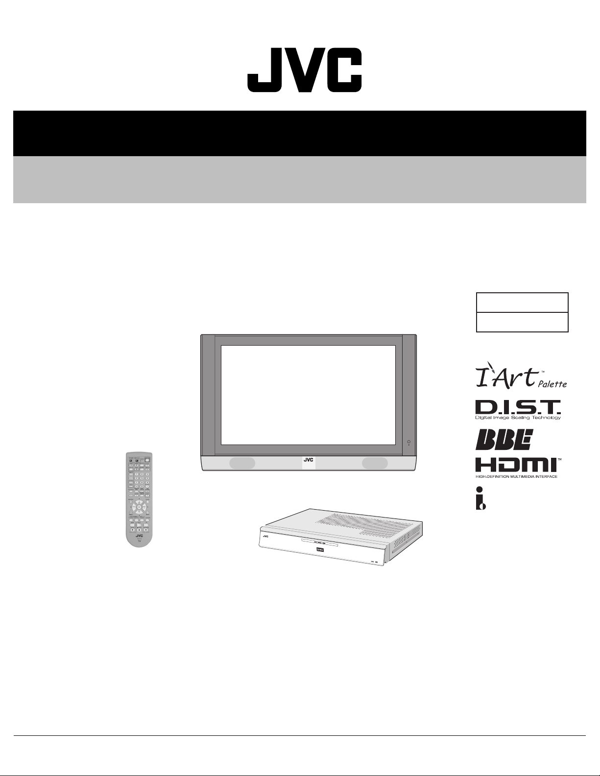
SERVICE MANUAL
PDP COLOR TELEVISION
YA10020052
PD-42X795/S,
PD-50X795
VM-42X795 / VM-50X795
[PLASMA DISPLAY UNIT]
P
O
WE
R
/Z
BASIC CHASSIS
FP2
TU-42X795 / TU-50X795
[RECEIVER UNIT]
TABLE OF CONTENTS
1 PRECAUTION. . . . . . . . . . . . . . . . . . . . . . . . . . . . . . . . . . . . . . . . . . . . . . . . . . . . . . . . . . . . . . . . . . . . . . . . . 1-3
2 SPECIFIC SERVICE INSTRUCTIONS . . . . . . . . . . . . . . . . . . . . . . . . . . . . . . . . . . . . . . . . . . . . . . . . . . . . . . 1-6
3 DISASSEMBLY . . . . . . . . . . . . . . . . . . . . . . . . . . . . . . . . . . . . . . . . . . . . . . . . . . . . . . . . . . . . . . . . . . . . . . 1-11
4 ADJUSTMENT . . . . . . . . . . . . . . . . . . . . . . . . . . . . . . . . . . . . . . . . . . . . . . . . . . . . . . . . . . . . . . . . . . . . . . . 1-28
5 TROUBLESHOOTING . . . . . . . . . . . . . . . . . . . . . . . . . . . . . . . . . . . . . . . . . . . . . . . . . . . . . . . . . . . . . . . . . 1-38
COPYRIGHT © 2005 Victor Company of Japan, Limited
No.YA100
2005/2
Page 2
SPECIFICATION
Items
Dimensions ( W × H × D ) Plasma Display Unit 116cm × 73.1cm × 10.8cm (45-3/4" × 28-7/8" × 4-1/4") 135cm × 83.6cm × 11cm (53-1/4" × 33" × 4-3/8")
Receiver Unit 43.5cm × 7cm × 31.3cm (17-1/4" × 2-7/8" × 12-3/8")
Mass Plasma Display Unit 38kg (83.6lbs) 51kg (112.2lbs)
Receiver Unit 4.3kg (9.5lbs)
TV RF System (Analog / Digital) Analog
Color System (Analog) NTSC
Sound System (Analog) BTSC (Multi Channel Sound)
Teletext System (Analog) Closed caption (T1-T4 / CC1-CC4)
TV Receiving Channels and
Frequency (Analog)
TV / CATV Total Channel 191 Channels
Intermediate Frequency (Analog) Video IF
Color Sub Carrier Frequency (Analog) 3.58 MHz
Power Input AC120V, 60Hz
Power Consumption Plasma Display Unit 387.4W (Max) / 369W (Avg) 491.4W (Max) / 468W (Avg)
Plasma Display Panel (PDP) 42V wide aspect (16:9) 50V wide aspect (16:9)
Screen Size Diagonal : 107.5cm (H:933cm × V : 53.3cm) Diagonal : 127.0cm (H:110.7cm × V : 62.2cm)
Display Pixels Horizontal : 1024 pixels × Vertical : 768 pixels (XGA) Horizontal : 1365 pixels × Vertical : 768 pixels (W-XGA)
Audio Power Output 20W + 20W
Speaker Main (DD)
Antenna terminal (VHF/UHF, ATSC / DIGITAL CABLE IN) F-type connector, 75Ω unbalanced, coaxial × 2
Video / Audio Input
[INPUT-1/2/3/4]
Digital Input Video
Audio Output
Monitor / Recording Output S-Video
PC (RGB) Input D-sub 15pin × 1
Center Channel Input 500mV(rms) (-4dBs), high impedance,RCA pin jack × 1
Sub woo fer Output More than 0 to 1000mV (rms) (+2.2dBs), low impedance (80Hz when modulated 100%), RCA pin jack × 1
Digital Audio Optical Output Digital SPDIF × 1
AV COMPULINK lll 3.5mm mini jack × 1
iLink Input/Output TS In/Out (4-pin, S400) × 2, IEEE1394 compliant DTCP digital copy protection compatible
Display Input / Output
(For system cable)
Remote Control Unit RM-C14G (AA/R6 / UM-3 battery × 2)
VHF Low
VHF High
Sound IF
Receiver Unit 39.9W (Max) / 38W (Avg)
Component Video
[INPUT-1/2]
1125i / 750p
525p / 525i
[INPUT-1/3/4]
Control / Audio
CCIR (M)
Digital
ATSC terrestrial / Digital cable
02ch - 06ch : 54MHz - 88MHz
07ch - 13ch : 174MHz - 216MHz
UHF
14ch - 69ch : 470MHz - 806MHz
CATV
54MHz - 804MHz
Low Band : 02 - 06
High Band : 07 - 13
Mid Band : 14 - 22
Super Band : 23 - 36
Hyper Band : 37 - 64
Ultra Band : 65 - 94, 100 - 135
Sub Mid Band : 01, 96 - 99
45.75 MHz
41.25 MHz (4.5MHz)
9.5cm × 1cm (3-3/4 × 7-7/16"), oval type × 2
Tweeter
2cm (13/16"), round type × 2
Woofer
13cm × 6.5cm (5-1/8 × 2-9/16"), oval type × 2
RCA pin jack × 6
Y : 1V (p-p) (Sync signal: 0.35V(p-p), 3-value sync.), 75 Ω
Pb/Pr : ±0.35V(p-p), 75 Ω
Y : 1V (p-p), positive (Negative sync), 75 Ω
Pb/Pr : 0.7V(p-p), 75 Ω
S-Video
Mini-DIN 4 pin × 3
Y: 1V (p-p), positive (Negative sync), 75 Ω
C: 0.286V (p-p) (Burst signal), 75 Ω
Video
1V (p-p), positive (Negative sync), 75 Ω, RCA pin jack × 4
Audio
500mV (rms), high impedance, RCA pin jack × 8
HDMI connector × 1
(Digital-input terminal is not compatible with picture signals of computer signal)
Audio
Digital: HDMI connector × 1
Anarog: 500mV(rms) (-4dBs), high impedance, RCA pin jack × 2
RCA pin jack × 2
Variable
More than 0 to 1000mV (rms) (+2.2dBs)
Fix
500mV(rms), (-4dBs), low impedance (400Hz when modulated 100%)
Mini-DIN 4pin × 1
Y: 1V (p-p), 75Ω
C: 0.286V(p-p) (burst signal), 75Ω
Video
1V (p-p), 75Ω, RCA pin jack × 1
Audio
250mV(rms) (-10dBs), Fs-18dB low impedance, RCA pin jack × 2
R/G/B : 0.7V (p-p), 75Ω
HD / VD : 1V (p-p) to 5V (p-p), high impedance
< Available signal >
VGA : 640 pixels × 480 pixels (Horizontal : 31.5kHz / Vertical : 60Hz)
XGA : 1024 pixels × 768 pixels (Horizontal : 48.4kHz / Vertical : 60Hz)
D-sub 26-pin connector × 2
Video
DVI-D 24-pin connector × 2
PD-42X795 PD-50X795
Contents
Design & specifications are subject to change without notice.
1-2 (No.YA100)
Page 3

SECTION 1
PRECAUTION
1.1 SAFETY PRECAUTIONS
(1) The design of this product contains special hardware,
many circuits and components specially for safety
purposes. For continued protection, no changes should be
made to the original design unless authorized in writing by
the manufacturer. Replacement parts must be identical to
those used in the original circuits. Service should be
performed by qualified personnel only.
(2) Alterations of the design or circuitry of the products should
not be made. Any design alterations or additions will void
the manufacturer's warranty and will further relieve the
manufacturer of responsibility for personal injury or
property damage resulting therefrom.
(3) Many electrical and mechanical parts in the products have
special safety-related characteristics. These
characteristics are often not evident from visual inspection
nor can the protection afforded by them necessarily be
obtained by using replacement components rated for
higher voltage, wattage, etc. Replacement parts which
have these special safety characteristics are identified in
the parts list of Service manual. Electrical components
having such features are identified by shading on the
schematics and by ( ) on the parts list in Service
manual. The use of a substitute replacement which does
not have the same safety characteristics as the
recommended replacement part shown in the parts list of
Service manual may cause shock, fire, or other hazards.
(4) Don't short between the LIVE side ground and
ISOLATED (NEUTRAL) side ground or EARTH side
ground when repairing.
Some model's power circuit is partly different in the GND.
The difference of the GND is shown by the LIVE : ( ) side
GND, the ISOLATED (NEUTRAL) : ( ) side GND and
EARTH : ( ) side GND.
Don't short between the LIVE side GND and ISOLATED
(NEUTRAL) side GND or EARTH side GND and never
measure the LIVE side GND and ISOLATED (NEUTRAL)
side GND or EARTH side GND at the same time with a
measuring apparatus (oscilloscope etc.). If above note will
not be kept, a fuse or any parts will be broken.
(5) If any repair has been made to the chassis, it is
recommended that the PDP POWER SUPPLY setting
should be checked or adjusted.
(6) The high voltage applied to the PDP must conform with that
specified in Service manual. Excessive high voltage can
cause an increase in arcing and possible component
damage, therefore operation under excessive high voltage
conditions should be kept to a minimum, or should be
prevented. If severe arcing occurs, remove the AC power
immediately and determine the cause by visual inspection
(incorrect installation, cracked or melted high voltage
harness, poor soldering, etc.). To maintain the proper
components in the circuitry including the PDP must be the
exact replacements or alternatives approved by the
manufacturer of the complete product.
(7) Do not check high voltage by drawing an arc. Use a high
voltage meter or a high voltage probe with a VTVM.
Discharge the picture tube before attempting meter
connection, by connecting a clip lead to the ground frame
and connecting the other end of the lead through a 10kΩ
2W resistor to the anode button.
(8) When service is required, observe the original lead dress.
Extra precaution should be given to assure correct lead
dress in the high voltage circuit area. Where a short circuit
has occurred, those components that indicate evidence of
overheating should be replaced. Always use the
manufacturer's replacement components.
(9) Isolation Check (Safety for Electrical Shock Hazard)
After re-assembling the product, always perform an
isolation check on the exposed metal parts of the cabinet
(antenna terminals, video/audio input and output terminals,
Control knobs, metal cabinet, screw heads, earphone jack,
control shafts, etc.) to be sure the product is safe to operate
without danger of electrical shock.
a) Dielectric Strength Test
The isolation between the AC primary circuit and all metal
parts exposed to the user, particularly any exposed metal
part having a return path to the chassis should withstand a
voltage of 3000V AC (r.m.s.) for a period of one second. (.
. . . Withstand a voltage of 1100V AC (r.m.s.) to an
appliance rated up to 120V, and 3000V AC (r.m.s.) to an
appliance rated 200V or more, for a period of one second.)
This method of test requires a test equipment not generally
found in the service trade.
b) Leakage Current Check
Plug the AC line cord directly into the AC outlet (do not use
a line isolation transformer during this check.). Using a
"Leakage Current Tester", measure the leakage current
from each exposed metal part of the cabinet, particularly
any exposed metal part having a return path to the chassis,
to a known good earth ground (water pipe, etc.). Any
leakage current must not exceed 0.5mA AC (r.m.s.).
However, in tropical area, this must not exceed 0.2mA AC
(r.m.s.).
Alternate Check Method
Plug the AC line cord directly into the AC outlet (do not
use a line isolation transformer during this check.). Use
an AC voltmeter having 1000Ω per volt or more
sensitivity in the following manner. Connect a 1500Ω
10W resistor paralleled by a 0.15µF AC-type capacitor
between an exposed metal part and a known good earth
ground (water pipe, etc.). Measure the AC voltage
across the resistor with the AC voltmeter. Move the
resistor connection to each exposed metal part,
particularly any exposed metal part having a return path
to the chassis, and measure the AC voltage across the
resistor. Now, reverse the plug in the AC outlet and
repeat each measurement. Any voltage measured must
not exceed 0.75V AC (r.m.s.). This corresponds to
0.5mA AC (r.m.s.).
However, in tropical area, this must not exceed 0.3V AC
(r.m.s.). This corresponds to 0.2mA AC (r.m.s.).
AC VOLTMETER
(HAVING 1000 /V,
OR MORE SENSITIVITY)
0.15 F AC-TYPE
PLACE THIS PROBE
1500 10W
GOOD EARTH GROUND
ON EACH EXPOSED
ME TAL PAR T
(No.YA100)1-3
Page 4
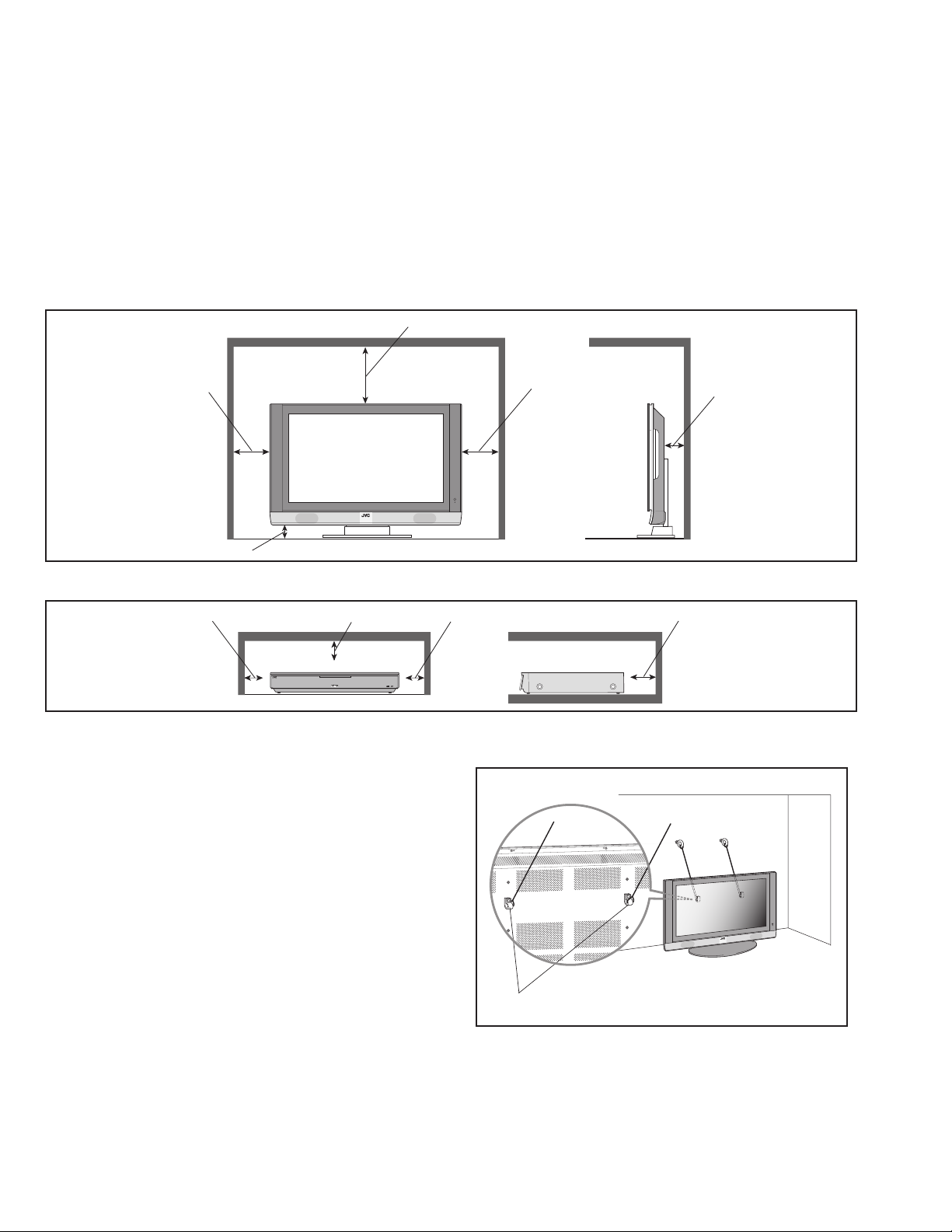
1.2 INSTALLATION
1.2.1 HEAT DISSIPATION
If the heat dissipation vent behind this unit is blocked, cooling efficiency may deteriorate and temperature inside the unit will rise. The
temperature sensor that protects the unit will be activated when internal temperature exceeds the pre-determined level and power will
be turned off automatically.
Therefore, please make sure pay attention not to block the heat dissipation vent as well as the ventilation outlet behind the unit and
ensure that there is room for ventilation around it.
1.2.2 INSTALLATION REQUIREMENTS
Ensure that the minimal distance is maintained, as specified below, between the unit with and the surrounding walls, as well as the
floor etc. Install the unit on stable flooring or stands. Take precautionary measures to prevent the unit from tipping in order to protect
against accidents and earthquakes.
SPACE REQUIRED FOR INSTALLATION OF THE DISPLAY UNIT
8 inch/200 mm
6 inch/150 mm
2 inch/50 mm
SPACE REQUIRED FOR INSTALLATION OF THE RECEIVER UNIT
4 inch/100 mm
POWER
PLASMA DISPLAY RECEIVER
4 inch/100 mm4 inch/100 mm 4 inch/100 mm
1.2.3 FALL TIP PREVENTION MEASURES
Take precautionary measures to prevent the unit from falling or
tipping to protect against emergencies such as earthquakes as
well as accidents.
Fasten the supplied hook for tip fall prevention using the screws,
also supplied, behind the display unit, and use them together
with durable cords (to be purchased separately) to secure the
unit to a robust part such as the wall surface or pillars.
6 inch/150 mm
2 inch/50 mm
1-4 (No.YA100)
The supplied hook for tipfall prevention
Page 5

1.3 PRECAUTIONS REGARDING PDP
1.3. 1 PRECAUTIONS DURING NOTES FOR TRANSPORTATION
When transporting the unit, pressure exerted on the internal PDP
(Plasma Display Panel) due to improper handling (such as
tossing and dropping) may cause damages even when the unit
is carefully packed. To prevent accidents from occurring during
transportation, pay careful attention prior to delivery such as
through explaining the handling instructions to transporters.
Ensure that the following requirements are met during
transportation, as the PDP of this unit is made of glass and
therefore fragile:
(1) Avoid vibrations and impacts
The unit may be broken if it is toppled sideways even when
properly packed. Ensure that the unit is carried by at least
2 persons and pay careful attention not to exert any
vibration or impact on it.
(2) Do not place equipment horizontally
Ensure that it is placed upright and not horizontally during
transportation and storage as the PDP is very vulnerable to
lateral impacts and may break easily under such
circumstances.
During transportation, ensure that the unit is loaded along
the traveling direction of travel of the vehicle, and avoid
stacking them on one another.
For storage, ensure that they are stacked in 2 layers or less
even when placed upright.
1.3.2 RESIDUAL IMAGE / BURN-IN ON SCREEN
Like CRTs, "burn-in" may occur when a same image is
continuously displayed over an extended period of time.
As this may also shorten the life span of the PDP. Therefore, turn
off the display when not in use, scroll the screen, make use of
screen-savers, or allow even distribution on the display by
inverting the brightness, switching to complementary colors or
inserting animated images at periodic intervals.
As burn-in is more likely to occur with high brightness and
contrast settings, try to use neutral gradations or medium tone
colors.
Burn-in does not occur in the case of animated images.
When switching to another image after continuous display of the
previous image, residual images may become prominent, as
luminance in a part of the display is higher than the other parts.
This is not a defect but is because due to the discharge surface
of the lighted portion has become being relatively activated and
its luminance higher than the unlighted parts.
1.3.4 OPTICAL FILTER (PANEL FILTER)
Avoid placing the unit under direct sunlight over a prolonged
period of time. This may cause the optical filter to deteriorate in
quality and color.
Clean the filter surface by wiping it softly lightly with outing
flannels a soft and lightly fuzz cloth (such as flannel).
Do not use solvents such as benzine or thinner to wipe the filter
surface. This may cause the filter to deteriorate in quality or the
coating on the surface to come off.
As the filter surface is fragile., do not scratch or hit it with hard
materials.
1.3.5 NOTES PRECAUTIONS FOR PEPLACEMENT OF
EXTERIOR PARTS
Take note of the following when replacing exterior parts (back
REAR COVER, FRONT PANEL, optical filter)
• Do not exert pressure on the front of the PDP (glass surface).
• Pay careful attention not to scratch or stain the front of the PDP
(surface) with hands.
• When replacing exterior parts, the front of the PDP should be
placed facing downward. Place a mat, etc. underneath to avoid
causing scratches to the front surface. However, never use
materials that are too soft (such as blanket cloth). If
replacement is made with the PDP surface facing downward
and in contact with the blanket, pressure may be exerted on
the PDP, thus causing damages to it.
1.3.3 INFRARED RAYS
Near Near-infrared rays (800nm to 1000nm) are emitted from the
front of the panel, and this may give rise to malfunctions in
infrared remote controls or communication systems placed near
it. In this case, avoid direct infrared rays (and reflected rays in
some cases) from the screen by either changing the direction of
the unit or other infrared systems or securing a longer keeping a
distance from the screen.
(No.YA100)1-5
Page 6
SECTION 2
LOB OK FAN OK
SYNC M:OK S:OK HD:NG
TIM OK
MSM OK DIGI 0000
MEM OK AVSW OK
YC OK AIO OK
TUN OK GCR NG 1
IP OK RGB OK 8
DVI OK HDMI OK
SERVICE MENU
1.ADJUST
2.SELF_CHK
3.I2C STOP
SPECIFIC SERVICE INSTRUCTIONS
2.1 FEATURES
D.I.S.T. (Digital Image Scaling Technology)
This system uses line interpolation to double the number of
scanning lines and achieve high resolution, flicker-free picture.
SMART CAPTION
Smart caption will appear when you press the MUTING button,
only on channels where the broadcast contains CLOSED
CAPTION information.
SMART SOUND
Decreases high sound levels, giving a regulated sound level.
VIDEO STATUS
Expression of a favorite screen can be chosen by the VIDEO
STATUS function.
[STANDARD ↔ DYNAMIC ↔ THEATER ↔ GAME]
DIGITAL INPUT
Digital-in will display when any picture signal (480i/ 480p,
720p/ 1080i) in Digital-in is displayed.
V-CHIP
Since the V-CHIP is built in, it can choose, view and listen to a
healthy program.
MTS STEREO
The voice multiplex function of the MTS system is built in.
(MTS = Multi channel Television Sound system)
NATURAL CINEMA
Watching the movie or animation, press the Natural Cinema to
adjust the out line of the images to make thin more sharp.
BBE
High definition audio adds natural, clear and extraordinary
sound quality to any program.
VIDEO INPUT LABEL
This function is used to label video input connections for the
onscreen displays.
A.H.S.
Adds a more spacious surround sound. Music gives basic
effect and Movie for more effect.
2.2 SYSTEM SETTEING
Be sure to carry out the following operation at the end of
the procedure.
(1) Set to 0 minutes using the [SLEEP TIMER] key.
(2) Press the [VIDEO STATUS] key and [DISPLAY] key
simultaneously, then enter the SERVICE MODE.
(3) When the Main Menu is displayed, press [2] key to enter
the self check mode.
(4) Turn off the power by pressing the [POWER] key on the
remote control unit.
MAIN MENU SCREEN
SERVICE MENU
1.ADJUST
2.SELF_CHK
3.I2C STOP
SELF CHECK MODE SCREEN
LOB OK FAN OK
SYNC M:OK S:OK HD:NG
TIM OK
MSM OK DIGI 0000
MEM OK AVSW OK
YC OK AIO OK
TUN OK GCR NG 1
IP OK RGB OK 8
DVI OK HDMI OK
1-6 (No.YA100)
Page 7
2.3 TECHNICAL INFORMATION
2.3.1 PDP STRUCTURE AND CHARACTERISTIC
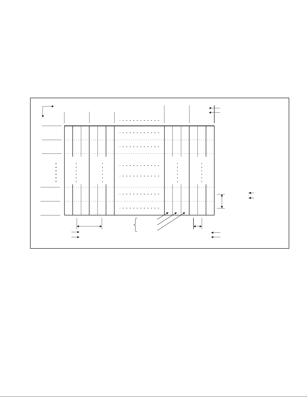
This unit uses the flat type panel PDP (Plasma Display Panel), instead of the conventional CRT (Cathode Ray Tube),
as a display unit.
2.3.1.1 PIXEL (CELL) ARRAY
PDP is constructed by sealing the xenon, which emits neon and ultraviolet rays for discharging purpose, in between the electrodes
lay on the front glass substrate and rear glass substrate.
One pixel is composed of 3 RGB cells, with cell pitch of 0.280mm (1 pixel 0.810mm) [PD-50X795] / 0.304 mm (1 plxel 0.912 mm) [PD-
42X795] horizontally and 0.810mm [PD-50X795] / 0.693 mm [PD-42X795] vertically.
The cell is arrayed in each RGB color as shown in Fig. 1. One pixel is formed by interlacing each RGB color cell.
One cell size is 0.280mm [PD-50X795] / 0.304 mm [PD-42X795] horizontally and 0.810mm [PD-50X795] / 0.693 mm [PD-42X795]
vertically.
Direction
Vertically
Horizontally
No.1
Pixel line
No.2
Pixel line
No.767
Pixel line
No.768
Pixel line
PD-50X795
PD-42X795
No.1365 No.1366
No.1
Pixel
sequence
No.2
Pixel
sequence
No.1023
Pixel
sequence
No.1024
Pixel
sequence
B G R B G R B GRBG R
BGRBGR BGRBGR
BGRBGR BGRBGR
BGRBGR BGRBGR
1 pixel
(1 dot)
0.810mm
0.921mm 0.304mm
(Horizontally) Pixel pitch
B Cell
G
Cell
R Cell
0.280mm
(Horizontally) Cell pitch
PD-50X795
PD-42X795
0.810mm PD-50X795
0.693mm PD-42X795
(Vertically)
Pixel pitch(Cell pitch)
PD-50X795
PD-42X795
Fig.1
2.3.1.2 PIXEL DEFECTS
Though PDP is made by means of ultra precise technology, there are cases whereby not all pixels (cell) will function properly. In some
cases, there may be defective pixels that do not light at all or the ones that always light on.
There are 3 types of Pixel defects, [Bright Dot Defects], [Dark Dot Defects] and [Flicker Dot Defects], as defined respectively in the
following:
(1) BRIGHT FAULT
In this pixel fault, a cell that should not light originally is lighting on and off.
For checking this pixel fault, input ALL BLACK SCREEN and find out the cell that is lighting on and off.
(2) DARK FAULT
In this pixel fault, a cell that should light originally is not lighting or lighting with the brightness twice as brighter as originally lighting.
For checking this pixel fault, input 100% of each R/G/B colour and find out the cell that is not lighting.
(3) FLICKER FAULT
In the pixel fault, a cell that should light originally or not light originally is flashing on and off.
For checking this pixel fault, input ALL BLACK SCREEN signal or 100% of each RGB colour and find out the cell that is flashing on
and off.
(No.YA100)1-7
Page 8

2.3.2 MAIN CPU PIN FUNCTION [IC7601 = DIGITAL SIGNAL PWB ASS'Y : RECEIVER UNIT]
Pin Pin name I/O Function Pin Pin name I/O Function
1 VHOLD1 I Data slice for main screen closed caption 51 NC O Not used
2 HFLT1 I/O LPF for main screen closed caption video input 52 NC O Not used
3 NC O Not used 53 NC O Not used
4 NC O Not used 54 NC O Not used
5 DIGR0 O R [0] for OSD 55 NC O Not used
6 TB1in I AC power for timer clock 56 NC O Not used
7 REMO I Remote control 57 NC O Not used
8 BYTE I Not used 58 NC O Not used
9 CNVss I CPU programming mode select [Normal = L] 59 NC O Not used
10 DIGG0 O G [0] for OSD 60 NC O Not used
11 DIGB0 O B [0] for OSD 61 NC O Not used
12 RESET I Reset for main CPU [Reset = L] 62 HSYNC I H. sync for OSD
13 Xout O System clock osillation (crystal) : 16MHz 63 NC O Not used
14 Vss - GND 64 VSYNC I V. sync for OSD
15 Xin I System clock osillation (crystal) : 16MHz 65 NC O Not used
16 VccI I 3.3V power supply 66 NC O Not used
17 OSC1 I Clock for OSD 67 NC O Not used
18 OSC2 O Not used 68 NC O Not used
19 INT1 I AV COMPULINK control 69 NC O Not used
20 INT0 I
21 OUT1 O Ys (blanking) for OSD 71 NC O Not used
22 OUT2 O YM (transparence) for OSD 72 NC O Not used
23 NC O Not used 73 NC O Not used
24 NC O Not used 74 NC O Not used
25 NC O Not used 75 NC O Not used
26 NC O Not used 76 NC O Not used
27 CTA2/RTS2 O Not used 77 NC O Not used
28 CLK2 O Not used 78 NC O Not used
29 RxD2 O Data transmission (serial) for digital tuner control 79 NC O Not used
30 TxD2 I Data receive (serial) for digital tuner control 80 NC O Not used
31 SDA2 I/O Not used 81 NC O Not used
32 DIGR1 O R [1] for OSD 82 NC O Not used
33 DIGG1 O G [1] for OSD 83 NC O Not used
34 DIGB1 O B [1] for OSD 84 WAKE O
35 TxD0 I Data receive (serial) for external programming 85 CARD_DET I Card detection for ATSC digital tuner [Detection = L]
36 RxD0 O Data transmission (serial) for external programming 86
37 CLK0 I Clock for external programming 87 SDAM I/O
38 RTS0 O Busy for external programming [Operation = H] 88 SCLM O
39 P5.7 I Not used 89 DIGR2 O R [2] for OSD
40 P5.6 O Not used 90 DIGG2 O G [2] for OSD
41 HOLD I CPU programming hold [Hold = H] 91 DIGB2 O B [2] for OSD
42 P5.4 O Not used 92 NC O Not used
43 P5.3 O Not used 93 KEY2 I Key scan data for display switch button KEY2
44 P5.2 O Not used 94 KEY1 I Key scan data for display switch button KEY1
45 P5.1 O Not used 95 VHOLD2 I Data slice for sub screen closed caption
46 WR O CPU programming mode select [Normal = L] 96 HLF2 I/O LPF for sub screen closed caption video input
47 P4.7 O
48 P4.6 I
49 P4.5 I Clock for sub(chassis) CPU communication (serial) 99 VCCE I 5V power supply
50 P4.4 O Not used 100 CVIN1 I Video(Y) for main screen closed caption
Request for sub(chassis) CPU communication (serial data)
Data transmission for sub(chassis) CPU communication (serial)
Data receive for sub(chassis) CPU communication (serial)
70 NC O Not used
Sleep mode release for sub(chassis) CPU [Release = L]
POWER_SW
97 CVIN2 I Video(Y) for sub screen closed caption
98 TVSETB I Test terminal [L Fixed]
I Power switch (mechanical) detection [Detection = L]
Data for Inter IC (serial) bus control : main memory (IC7602)
Clock for Inter IC (serial) bus control : mainmemory (IC7602)
1-8 (No.YA100)
Page 9
2.3.3 SUB (CHASSIS) CPU PIN FUNCTION [IC7001 = DIGITAL SIGNAL PWB ASS'Y : RECEIVER UNIT]
Pin Pin name I/O Function Pin Pin name I/O Function
1 LB_PRO O Not used 51 BS_TXD O Data transmission for digital tuner communication
2 P_MU O Picture muting [Muting = H] 52 BS_RXD I Data receive for digital tuner communication
3 JP_CSB O Not used 53 NC O Not used
4 A_MU O Audio muting (for AUDIO OUT) [Muting = H] 54 VREF+ I 3.3V power supply
5 M_MU O Audio muting (for MONITOR OUT) [Muting = H] 55 PDP_TX O
6 PC_SEL O RGB(PC) INPUT select [ON = H] 56 PDP_RX I Data receive for
7 ON_TIMER O POWER INDICATOR (LED) brightness [LOW = L] 57 SDA0 I/O Data for Inter IC (serial) bus : sub memory (IC7002)
8 ILA0 O Not used 58 SCL0 O Clock for Inter IC (serial) bus : sub memory (IC7002)
9 ILA1 O Not used 59 SDA_DVI I/O Data for Inter IC (serial) bus for panel communication
10 ILA2 O Not used 60 SCL_DVI O Clock for Inter IC (serial) bus for panel communication
11 POW_LED O POWER LED lighting [ON = H] 61 AVSS - GND
12 WORD O Not used 62 DIGI_PHOT I Photo sensor for DIGITAL-IN illegal copy protection
13 MI_CK I Clock for main CPU communication 63 AGC I Not used
14 MI_TX I Data receive for main CPU communication 64 EXT_YS1 I Not used
15 MI_RX O Data transmission for main CPU communication 65 EXT_YS2 I Not used
16 MI_REQ O
17 VDD I 3.3V power supply 67 DIGI_PRO O DIGITAL-IN voltage detection [Detection = H]
18 FOSC O Not used 68 GCR_RST O Not used
19 VSS - GND 69 GR_ON O Not used
20 X1 I 3.3V power supply 70 SYNC_SEL O Multi screen control [Digital = L]
21 X0 O Not used 71 NC O Not used
22 VDD I 3.3V power supply 72 NC O Not used
23 OSC1 I System clock osillation (crystal) : 16MHz 73 SBD5 I/O
24 OSC0 O System clock osillation (crystal) : 16MHz 74 SBT5 I
25 MODE I 3.3V power supply 75 NMI I 3.3V power supply
26 BS1.5CTL O Digital tuner power control [ON = H] 76 COMP I Not used
27 A92RES O
28 BS_RST O Reset for Digital tuner [Reset = L] 78 VSYNC I V. sync pulse
29 LIP_RST O Not used 79 WAKE I
30 SOFT_OFF O Not used 80
31 VMUTE I Picture muting request from digital tuner [Muting = L] 81 NC O Not used
32 VOUTENB O Video cutoff for digital tuner [Cufoff = H] 82 RST I Reset for
33 MDR_CON I System cable connection monitor for display unit (PDP) 83 VDD I 3.3V power supply
34 AVDD I 3.3V power supply 84 SCL3A O Clock for Inter IC (serial) bus control
35 BS_POW O Not used 85 SDA3A I/O Data for Inter IC (serial) bus control
DsyncSW2
36
37 LB_POW O Not used 87 SDA3B I/O Data for Inter IC (serial) bus control
38 NC O Not used 88
39 HOTPLUG I Video communiation monitor for display unit (PDP) 89 DIGI_LRSW O DIGITAL-IN control
40 MECA_SW I Mechanical monitor for POWER switch [Push = L] 90 DIGI_INT I Reset for HDMI process [Reset = L ]
41 MAIN_POW O Main power control [ON = L] 91 DVI_RST O Reset for DVI format conversion
42 MSP_RST O AUDIO OUT output mode select [VARIABLE = L] 92 VSS - GND
43 VREF- I Standard Voltage (0V) power supply 93 SCL5055 O
44 AFT2 I Not used 94
45 AFT1 I AFT voltage for VHF/UHF tuner 95 SDA5055 I/O Data for Inter IC (serial) bus : JCC5055 (DIST process)
46 KEY2 I Not used 96
47 KEY1 I Not used 97 NC O Not used
48 NC O Not used 98 15K/OTH O Main video select [Fixed H]
49 NC O Not used 99 DsyncSW1 O Sync select for DIGITAL-IN [Cotrolled with 36-pin]
50 AC_IN I AC power pulse for timer clock 100 57 BUSY I Busy monitor for JCC5057 (RGB process)
Data request for main CPU communication [Request = L]
Reset for IC1001(3D YC SEP / COLOR DEMODULAT) [Reset = H]
O Sync select for DIGITAL-IN [Cotrolled with 99-pin] 86 SCL3B O Clock for Inter IC (serial) bus control
66 VDD I 3.3V power supply
77 REMO I Remote control
POWERGOOD
DIGI_SYNCSEL
VFORMATSEL
OSD_MODE_SEL
Data transmission for panel CPU communication
panel
CPU communication
Data for writing on board (connect CN01P : for Frash ROM type)
Clock for writing on board (connect CN01P : for Frash ROM type)
Sleep mode release for sub(chassis) CPU [Release = L]
I Power error detection NG = H]
sub(chassis)
O Not used
Clock for Inter IC (serial) bus : JCC5055 (DIST process)
O Not used
O Not used
CPU [Reset = L]
(No.YA100)1-9
Page 10
2.3.4 PANEL CPU PIN FUNCTION [IC807 = DISPLAY INTERFACE PWB ASS'Y : DISPLAY UNIT]
Pin Pin name I/O Function Pin Pin name I/O Function
1 SYSTEM0 I PDP size select [0V=50V XGA, 1.75V=42V XGA] 34 NC O Not used
2 SYSTEM3 I PDP maker select [0V=SAMSUNG, 1.75V=LG] 35 NMI I Port for writing on board control [Writing=L]
3 AVCC - 5.0V power suplly 36 A_MU O Audio muting [Muting=H]
4 X2 - Not used 37 HD I Not used
5X1 -GND 38
6 VCL - GND 39 REMO I Not used
7 RES I Reset for panel CPU [Reset=L] 40 LED_POW O POWER LED control [ON=H]
8 TEST I GND 41 P85 I
9 VSS - GND 42 P86 - Emulator connection
10 OSC2 O System clock osillation (crystal) : 16MHz 43 P87 - Emulator connection
11 OSC1 I System clock osillation (crystal) : 16MHz 44 SCK3 O Clock for writing on board
12 VCC - 5.0V power suplly 45 RXD I Data receive for writing on board
13 PW_LOB O Power control [ON=L] 46 TXD O Data trnsmission for writing on board
PANEL_PW_ON
14
15 NC O Not used 48 NC O Not used
16 NC O Not used 49 RXD2 I Data receive for main CPU communication
17 I2C_STOP O Inter IC (serial) bus stop control [Stop=L] 50 TXD2 O Data transmission for main CPU communication
18 APL_S_CLK O Clock for APS loading [PD-50X795] 51 IRQ O Sleep mode release [Rlease=H]
19 PSCK O Clock for APS writing [PD-50X795] 52 ACTIVE I Power switch (mechanical) detection [Detection=H]
20 PLE O APS loading control [PD-50X795] 53 VD I V. sync pulse
21 CLE O APS writing control [PD-50X795] 54 REC_DET I System cable monitor for receiver unit [Connection=L]
22 PSSC O Data transmission for APS loading [PD-50X795]
23 SDA1 I/O
24 PWM O Not used
25 SCL1 O
26 SDA0 I/O
27 SCL0 O
28 SDA2 I/O
29 SCL2 O
30 SLE O PDP communication control [PD-50X795] 61 AMP_PRO1 I Not used
31 NC I/O Not used 62 EE_CDS I Not used
32 NC O Not used 63 KEY1 I Not used
33 NC O Not used 64 KEY2 I Not used
O Panel power control [ON=L] 47 AC_DET I AC power frequency detection [Detection=H]
Data for Inter IC (serial) bus control : panel memory (IC805)
Clock for Inter IC (serial) bus control : panel memory (IC805)
Data for Inter IC (serial) bus control : Audio control, Temp. sensor
Clock for Inter IC (serial) bus control : Audio control, Temp. sensor
Data for Inter IC (serial) bus control : PDP communication
Clock for Inter IC (serial) bus control : PDP communication
LED_ONTIMER
55 PSS
56 FAN_LOCK I Fan abnormality detection [Detection=L] [PD-50X795]
57 SYSTEM2 I Not used
58 SYSTEM 1 I Fan select [Used=H]
59 THEM_DET I Temp. sensor detection [Detection=H]
60
(AMP_PRO2)
O POWER LED stand-by control [ON=H]
Emulator connection / Port for writing on board [Writing=H]
I PDP Inter IC (serial) bus communication select
[Permission=H][PD-42X795],
Data receive for APS loading [PD-50X795]
IGND
1-10 (No.YA100)
Page 11

SECTION 3
DISASSEMBLY
3.1 DISASSEMBLY PROCEDURE [DISPLAY UNIT: PD-42X795]
NOTE:
• When exchanging parts etc. with the front side (PDP side) fancing down, place a protection sheet under the DISPALY UNIT to
prevent scratches on the front side.
• It is advisable to take notes of the connecting locations (connector numbers) of the removed connectors.
3.1.1 REMOVING THE REAR COVER (Fig.1)
(1) Remove the power cord and system cable.
(2) Remove the 9 screws [A] and the 12 screws [B], then
remove the REAR COVER.
3.1.2 REMOVING THE BACK COVER AND SPEAKER
HOLDER (Fig.1)
(1) Remove the 8 screws [C], then remove the BACK COVER.
(2) Remove the SPEAKER HOLDER.
3.1.3 REMOVING THE TERMINAL COVER (Fig.1.)
• Remove the REAR COVER.
(1) Remove the 6 screws [D], then remove the CHASSIS
SHIELD BRACKET.
(2) Remove the 2 screws [E] and the 5 screws [F], then
remove the TERMINAL COVER.
3.1.4 REMOVING THE LINE FILTER PWB (Fig.1)
• Remove the REAR COVER.
• Remove the CHASSIS SHIELD BRACKET.
• Remove the TERMINAL COVER.
(1) Remove the 2 claws [G], then remove the LINE FILTER
INSULATOR.
(2) Disconnect the connector [CN8001
POWER PWB .
(3) Remove the 2 screws [H] and the 2 screws [I], then remove
the LINE FILTER PWB.
] from the MAIN
3.1.6 REMOVING THE DISPLAY INTERFACE PWB (Fig.1)
• Remove the REAR COVER.
• Remove the CHASSIS SHIELD BRACKET.
• Remove the TERMINAL COVER.
(1) Disconnect the connectors [CN00A
[CN00E
[CNAH2
(2) Remove the 4 screws [K], the 2 screws [L] ,and the 2
screws [M], then remove the DISPLAY INTERFACE PWB.
3.1.7 REMOVING THE CHASSIS BASE PWB (Fig.1.)
• Remove the REAR COVER.
• Remove the CHASSIS SHIELD BRACKET.
• Remove the TERMINAL COVER.
• Remove the LINE FILTER PWB.
• Remove the AUDIO PWB.
• Remove the DISPLAY INTERFACE PWB.
(1) Remove the 2 screws [N], then remove the CHASSIS
BASE PWB.
] / [CN00Q] / [CN00T] / [CN00X] / [CN00V] /
] from the DISPLAY INTERFACE PWB .
] / [CN00C] / [CN00D] /
3.1.5 REMOVING THE AUDIO PWB (Fig.1)
• Remove the REAR COVER.
• Remove the CHASSIS SHIELD BRACKET.
• Remove the TERMINAL COVER.
(1) Disconnect the connectors [CN60SL
[CN60SR
(2) Disconnect the connector [CN9001
PWB.
(3) Disconnect the connector [CN00A
from the DISPLAY INTERFACE PWB .
(4) Remove the 4 screws [J], then remove the AUDIO PWB.
] from the AUDIO PWB .
] / [CN60CB] /
] from the SUB POWER
] / [CN00C] / [CN00D]
(No.YA100)1-11
Page 12
REAR COVER
A
BACK COVER
C
C
BACK COVER
B
CHASSIS SHIELD
BRACKET
K
DISPLAY
INTERFACE
PWB
J
INSULATOR
D
AUDIO
PWB
LINE
FILTER
PWB
A
G
TERMINAL
I
H
a
N
COVER
I
E
F
F
F
E
F
TOP
SPEAKER HOLDER
N
CHASSIS BASE
M
L
a
SPEAKER HOLDER
Fig.1
1-12 (No.YA100)
Page 13

3.1.8 REMOVING THE TEMP. SENSOR PWB (Fig.2)
• Remove the REAR COVER.
(1) Disconnect the connector [CN800V
SENSOR PWB PWB .
(2) Remove the 1 screw [O], then remove the TEMP.
SENSOR PWB.
3.1.9 REMOVING THE MAIN POWER PWB (Fig.2)
• Remove the REAR COVER.
(1) Disconnect the connector [CN8001
/ [CN8005
from the MAIN POWER PWB .
(2) Remove the 8 screws [P], then remove the MAIN POWER
PWB.
(3) Remove the POWER PWB BRACKET and INSULATOR.
3.1.10 REMOVING THE SUB POWER PWB (Fig.2)
• Remove the REAR COVER.
(1) Disconnect the connector [CN9001
from the SUB POWER PWB .
(2) Remove the 4 screws [Q], then remove the SUB POWER
PWB.
(3) Remove the INSULATOR.
3.1.11 REMOVING THE DISPLAY SWITCH PWB (Fig.2)
• Remove the BACK COVER.
• Remove the SPEAKER HOLDER.
(1) Remove the 2 screws [U] and 3 screws [V], then remove
the DISPLAY SWITCH PWB and CONTROL KNOB.
(2) Disconnect the connector [CN000T
SWITCH PWB .
3.1.12 REMOVING THE DISPLAY LED PWB (Fig.2)
• Remove the BACK COVER.
• Remove the SPEAKER HOLDER.
• Remove the DISPLAY SWITCH PWB.
(1) Remove the 2 screws [T], then remove the DISPLAY LED
PWB.
(2) Disconnect the connector [CN000X
LED PWB .
] / [CN8003] / [CN8002] / [CN9001] / [CN8009]
] from the TEMP.
] / [CN8008] / [CN8006]
] / [CN9002] / [CN9005]
] from the DISPLAY
] from the DISPLAY
3.1.14 REMOVING THE WOOFER SPEAKER (Fig.2)
• Remove the REAR COVER.
(1) Disconnect the connector [CN60CB
PWB.
(2) Remove the 6 screws [V], then remove the WOOFER
SPEAKER UNIT.
(3) Remove the 8 screws [W], then remove the DUCT
COVER.
(4) Remove the 12 screws [X], then remove the WOOFER
BACK COVER.
(5) Remove the 8 screws [Y], then remove the WOOFER
SPEAKER.
3.1.15 REMOVING THE PDP (PANEL) UNIT (Fig.2)
• Remove the REAR COVER.
• Remove the CHASSIS SHIELD BRACKET.
• Remove the TERMINAL COVER.
• Remove the CHASSIS BASE(with each PWB affixed on the
CHASSIS BASE).
• Remove the TEMP. SENSOR.
• Remove the MAIN POWER PWB.
• Remove the SUB POWER PWB.
(1) Disconnect the connector [CN60SL
[CN60SR] from the AUDIO PWB .
(2) Disconnect the connector [CN00A] / [CN00C] / [CN00D] /
[CN00E
[CNAH2] from the DISPLAY INTERFACE PWB.
(3) Remove the 16 screws [Z], then remove the BACK
BRACKET.
(4) Lift the PDP upright and remove it with enough care not to
impose shock to the PDP.
CAUTION:
• Two or more people are required to remove the PDP unit.
• The gas pouring port is covered with the protection
material.In operation, be careful not to damage the gas
pouring port.
• Do not touch the front side (glass) of the PDP with your
fingers.
] / [CN00Q] / [CN00T] / [CN00X] / [CN0V] /
] from the AUDIO
] / [CN60CB] /
3.1.13 REMOVING THE DD SPEAKER (Fig.2)
• Remove the REAR COVER.
• Remove the BACK COVER.
• Remove the SPEAKER HOLDER.
(1) Disconnect the connector [CN60SR
AUDIO PWB .
(2) Remove the 4 screws [U], then remove the DD SPEAKER.
] / [CN60SL] from the
(No.YA100)1-13
Page 14

BACK FRAME
Z
BRACKET
Q
INSULATOR
SUB POWER PWB
INSULATOR
Z
P
Q
TEMP.
SENSOR PWB
O
P
MAIN POWER PWB
P
POWER PWB
BRACKET
INSULATOR
Z
BACK FRAME
BRACKET
Z
U
GAS insertion
hole
DD SPEAKER
INSULATOR
DISPLAY
SWITCH
PWB
CONTROL
KNOB
PDP UNIT
U
DD SPEAKER
T
W
DISPLAY LED PWB
DUCT COVER
W
R
S
DUCT
X
WOOFER BACK
COVER
COVER
X
Y
WOOFER
V
SPEAKER
1-14 (No.YA100)
TOP
Y
WOOFER
SPEAKER
Fig.2
Page 15

3.1.16 REMOVING THE PWB IN PDP UNIT
Y
3.1.16.1 REMOVING THE LOGIC-BUFFER-E PWB (Fig.3)
• Remove the PDP UNIT.
(1) Disconnect the connector [CN806
[CN2502
] / [CN2503] / [CN2504] / [CN2505] / [CN2506] /
] / [CN2500] / [CN2501] /
[CN2507] / [EF1] from the LOGIC-BUFFER-E PWB .
(2) Remove the 14 screws [a], then remove the LOGIC-BUFF-
ER-E PWB.
3.1.16.2 REMOVING THE LOGIC-BUFFER-F PWB (Fig.3)
• Remove the PDP UNIT.
(1) Disconnect the connector [CN402
[CN2601
[CN2606
] / [CN2602] / [CN2603] / [CN2604] / [CN2605] /
] / [CN2607] / [FE1] from the LOGIC-BUFFER-F
] / [CN807] / [CN2600] /
PWB .
(2) Remove the 14 screws [b], then remove the LOGIC-BUFF-
ER-F PWB.
3.1.16.3 REMOVING THE X-MAIN PWB (Fig.3.)
• Remove the PDP UNIT.
(1) Disconnect the connector [CN4001
] / [CN4002] / [CN4003]
/ [CN4004] / [CN4005] from the X-MAIN PWB .
(2) Remove the 8 screws [c], then remove the X-MAIN PWB.
3.1.16.4 REMOVING THE LOGIC-MAIN PWB (Fig.3)
• Remove the PDP UNIT.
(1) Disconnect the connector [CN2001
/ [CN2004
] / [CN2005] / [CN2006] / [CN207] / [LA1] from
] / [CN2002] / [CN2003]
the LOGIC-MAIN PWB .
Remove the 6 screws
(2)
[d]
, then remove the LOGIC-MAIN PWB.
3.1.16.5 REMOVING THE Y-MAIN PWB (Fig.3.)
• Remove the PDP UNIT.
(1) Disconnect the connector [CN5001
] / [CN5002] / [CN5003]
/ [CN5004] / [CN5005] / [CN5006] / [CN5007] / [CN5008]
from the Y-MAIN PWB .
(2) Remove the 7 screws [e], then remove the Y-MAIN PWB.
3.1.16.6 REMOVING THE Y-BUFFER-U PWB (Fig.3)
• Remove the PDP UNIT.
Disconnect the connector [CN5401] / [CN5402] / [CN5403] /
(1)
[CN5404
(2)
Remove the 3 screws
] / [CN5405] / [CN5407] from the Y-BUFFER-U PWB.
[f]
,then remove the Y-BUFFER-U PWB
3.1.16.7 REMOVING THE Y-BUFFER-L PWB (Fig.3)
• Remove the PDP UNIT.
Disconnect the connector [CN5501] / [CN5502] / [CN5503] /
(1)
[CN5504
(2)
Remove the 3 screws
] / [CN5505] / [CN5507] from the Y-BUFFER-L PWB.
[g]
, then remove the Y-BUFFER-L PWB
.
.
LOGIC-BUFFER-F PWB
e
f
-BUFFER-U PWB
Y-MAIN PWB
LOGIC-BUFFER-E PWB
a
b
g
Y-BUFFER-L PWB
d
a
LOGIC-BUFFER-E PWB
Fig.3
c
X-MAIN PWB
b
LOGIC-BUFFER-F PWB
LOGIC-MAIN PWB
(No.YA100)1-15
Page 16

3.1.17 REMOVING THE FRONT FILTER (Fig.4.)
• Remove the REAR COVER.
• Remove the CHASSIS SHIELD BRACKET.
• Remove the TERMINAL COVER.
• Remove the CHASSIS BASE (with each PWB affixed on the
CHASSIS BASE).
• Remove the TEMP. SENSOR.
• Remove the MAIN POWER PWB.
• Remove the SUB POWER PWB.
• Remove the PDP UNIT.
(1) Remove the 12 screws [h], then remove the GLASS
HOLDER.
(2) Remove the FRONT FILTER with enough care not to
damage it.
3.1.18 REMOVING THE TOP FRAME BRACKET, BOTTOM
FRAME BRACKET AND SIDE FRAME BRACKET (Fig.4.)
• Remove the REAR COVER.
• Remove the CHASSIS SHIELD BRACKET.
• Remove the TERMINAL COVER.
• Remove the CHASSIS BASE (with each PWB affixed on the
CHASSIS BASE).
• Remove the TEMP. SENSOR.
• Remove the MAIN POWER PWB.
• Remove the SUB POWER PWB.
• Remove the PDP UNIT.
• Remove the FRONT FILTER.
Remove the 6 screws
(1)
[i], then remove
the FRONT PANEL
.
(2) Remove the 4 spacers [j], the 4 screws [k], then remove
the TOP FLAME BRACKET, BOTTOM FLAME BRACKET
and SIDE FLAME BRACKET.
GLASS HOLDER
SIDE FRAME
BRACKET
h
i
j
TOP FRAME
BRACKET
j
i
k
j
SIDE FRAME
BRACKET
BOTTOM FRAME
BRACKET
i
j
i
k
h
1-16 (No.YA100)
FRONT FILTER
TOP
FRONT PANEL
Fig.4
Page 17

3.2 DISASSEMBLY PROCEDURE [DISPLAY UNIT: PD-50X795]
NOTE:
• When exchanging parts etc. with the front side (PDP side) fancing down, place a protection sheet under the DISPALY UNIT to
prevent scratches on the front side.
• It is advisable to take notes of the connecting locations (connector numbers) of the removed connectors.
3.2.1 REMOVING THE REAR COVER (Fig.5)
(1) Remove the power cord and the system cable.
(2) Remove the 11 screws [A] and the 22 screws [B], then
remove the REAR COVER.
3.2.2 REMOVING THE BACK COVER AND SPEAKER
HOLDER (Fig.5)
(1) Remove the 8 screws [C], then remove the BACK COVER.
(2) Remove the SPEAKER HOLDER.
3.2.3 REMOVING THE TERMINAL COVER (Fig.5)
• Remove the REAR COVER.
(1) Remove the 6 screws [D], then remove the CHASSIS
SHIELD BRACKET.
(2) Remove the 2 screws [E] and the 5 screws [F], then
remove the TERMINAL COVER.
3.2.4 REMOVING THE LINE FILTER PWB (Fig.5)
• Remove the REAR COVER.
• Remove the CHASSIS SHIELD BRACKET.
• Remove the TERMINAL COVER.
(1) Remove the 2 claws [G], then remove the LINE FILTER
INSULATOR.
(2) Disconnect the connector [CN8001
POWER UNIT.
(3) Remove the 2 screws [H] and 2 screws [I], then remove the
LINE FILTER PWB.
] from the MAIN
3.2.6 REMOVING THE DISPLAY INTERFACE PWB (Fig.5)
• Remove the REAR COVER.
• Remove the CHASSIS SHIELD BRACKET.
• Remove the TERMINAL COVER.
(1) Disconnect the connector [CN00A
[CN00E] / [CN00G] / [CN00Q] / [CN00T] / [CN00X] /
[CN00V
DISPLAY INTERFACE PWB .
(2) Remove the 3 screws [K], the 2 screws [L] and 2 screws
[M] , then remove the DISPLAY INTERFACE PWB.
3.2.7 REMOVING THE CHASSIS BASE (Fig.5)
• Remove the REAR COVER.
• Remove the CHASSIS SHIELD BRACKET.
• Remove the TERMINAL COVER.
• Remove the LINE FILTER PWB.
• Remove the AUDIO PWB.
• Remove the DISPLAY INTERFACE PWB.
(1) Remove the 2 screws [N], then remove the CHASSIS
BASE.
] / [CN0FL] / [CN0FR] / [CN601] / [CNAH1] from the
] / [CN00C] / [CN00D] /
3.2.5 REMOVING THE AUDIO PWB (Fig.5.)
• Remove the REAR COVER.
• Remove the CHASSIS SHIELD BRACKET.
• Remove the TERMINAL COVER.
(1) Disconnect the connector [CN60SL
[CN60SR
(2) Disconnect the connector [CN9001] from the SUB POWER
PWB.
(3) Disconnect the connector [CN00A
from the DISPLAY INTERFACE PWB.
(4) Remove the 4 screws [J], then remove the AUDIO PWB.
] from the AUDIO PWB .
] / [CN60CB] /
] / [CN00C] / [CN00D]
(No.YA100)1-17
Page 18

BACK COVER
C
B
A
A
REAR COVER
C
G
INSULATOR
BACK COVER
CHASSIS SHIELD
BRACKET
D
DISPLAY
INTERFACE
PWB
K
N
CHASSIS BASE
J
LINE
FILTER
PWB
L
AUDIO
PWB
H
N
M
I
I
TERMINAL
COVER
E
F
F
E
F
F
TOP
1-18 (No.YA100)
SPEAKER HOLDER
SPEAKER HOLDER
Fig.5
Page 19

3.2.8 REMOVING THE TEMP. SENSOR PWB (Fig.6)
• Remove the REAR COVER.
(1) Disconnect the connector [CN800V
SENSOR PWB PWB .
(2) Remove the 1 screw [O], then remove the TEMP.
SENSOR PWB.
3.2.9 REMOVING THE MAIN POWER UNIT (Fig.6)
• Remove the REAR COVER.
(1) Disconnect the connector [CN805
[CN8009
UNIT .
(2) Remove the 8 screws [P], then remove the MAIN POWER
UNIT.
3.2.10 REMOVING THE SUB POWER PWB (Fig.6)
• Remove the REAR COVER.
(1) Disconnect the connector [CN9001
from the SUB POWER PWB .
(2) Remove the 4 screws [Q], then remove the SUB POWER
PWB.
3.2.11 REMOVING THE COOLING FAN (Fig.6)
• Remove the REAR COVER.
(1) Disconnect the connector [CN0FL
DISPLAY INTERFACE PWB .
(2) Remove the 4 screws [R], then remove the COOLING FAN
BRACKET by lifting upward.
(3) Remove the 4 screws [S], then remove the COOLING FAN
by pulling in hte arrowed direction.
3.2.12 REMOVING THE POWER CHASSIS BASE (Fig.6)
• Remove the REAR COVER.
• Remove the MAIN POWER UNIT.
• Remove the SUB POWER PWB.
• Remove the COOLING FAN.
(1) Remove the 5 screws [T], then remove the POWER
CHASSIS BASE.
3.2.13 REMOVING THE DISPLAY SWITCH PWB (Fig.6)
• Remove the BACK COVER.
• Remove the SPEAKER HOLDER.
(1) Remove the 2 screws [U] and the 3 screws [V], then
remove the DISPLAY SWITCH PWB and CONTROL
KNOB.
(2) Disconnect the connector [CN000T
SWITCH PWB .
] / [CN8011] / [CN9001] from the MAIN POWER
] from the TEMP.
] / [CN806] / [CN8001] /
] / [CN9002] / [CN9005]
] / [CN0FR] from the
] from the DISPLAY
3.2.14 REMOVING THE DISPLAY LED PWB (Fig.6)
• Remove the BACK COVER.
• Remove the SPEAKER HOLDER.
• Remove the DISPLAY SWITCH PWB.
(1) Remove the 2 screws [W], then remove the DISPLAY LED
PWB.
(2) Disconnect the connector [CN000X
LED PWB .
3.2.15 REMOVING THE DD SPEAKER (Fig.6)
• Remove the REAR COVER.
• Remove the BACK COVER.
• Remove the SPEAKER HOLDER.
(1) Disconnect the connector [CN60SR
AUDIO PWB .
(2) Remove the 4 screws [X], then remove the DD SPEAKER.
3.2.16 REMOVING THE WOOFER SPEAKER (Fig.6)
• Remove the REAR COVER.
(1) Disconnect the connector [CN60CB
PWB.
(2) Remove the 6 screws [Y], then remove the WOOFER
SPEAKER UNIT.
(3) Remove the 8 screws [Z], then remove the DUCT COVER.
(4) Remove the 10 screws [a] and the 4 screws [b], then
remove the WOOFER BACK COVER.
(5) Remove the 8 screws [c], then remove the WOOFER
SPEAKER.
3.2.17 REMOVING THE PDP (PANEL) UNIT (Fig.6)
• Remove the REAR COVER.
• Remove the CHASSIS SHIELD BRACKET.
• Remove the TERMINAL COVER.
• Remove the CHASSIS BASE (with each PWB affixed on the
CHASSIS BASE).
• Remove the POWER CHASSIS BASE (with each PWB affixed
on the CHASSIS BASE).
• Remove the TEMP. SENSOR.
(1) Remove the 16 screws [d], then remove the BACK
BRACKET.
(2) Remove the 4 screws [e] then Lift the PDP straight upward
and remove it with extra attention no to impose any shock
to the PDP.
CAUTION:
• More than two people are required to remove the PDP unit.
• The gas pouring port is covered with the protection material.
Durring the operation, be careful not to damage the gas
pouring port.
• Do not touch the front side (glass) of the PDP with your
fingers.
] from the DISPLAY
] / [CN60SL] from the
] from the AUDIO
(No.YA100)1-19
Page 20

P
SUB POWER PWB
d
d
BACK BRACKET
e
GAS insertion
hole
INSULATOR
d
PDP UNIT
Q
R
T
d
TEMP. SENSOR PWB
O
FAN
BRACKET
FAN
S
CHASSIS BASE
MAIN POWER UNIT
FAN
R
BRACKET
COOLING FAN
S
T
d
e
BACK BRACKET
DD SPEAKER
d
d
d
e
X
DISPLAY
SWITCH
PWB
CONTROL
KNOB
U
e
INSULATOR
TOP
X
DD SPEAKER
W
DISPLAY LED PWB
Z
DUCT
COVER
a
b
V
DUCT
COVER
a
b
c
WOOFER
BACK COVER
Y
WOOFER
SPEAKER
WOOFER
SPEAKER
c
1-20 (No.YA100)
Fig.6
Page 21

3.2.18 REMOVING THE PWB IN PDP UNIT
Y
3.2.18.1 REMOVING THE X-LEFT-TOP PWB (Fig.7)
• Remove the PDP UNIT.
(1) Disconnect the connector [P4
] / [P5] / [P501] / [P502] /
[P503] / [P504] from the X-LEFT TOP PWB .
(2) Remove the 2 screws [f] and the 1 screw [g], then remove
the X-LEFT-TOP PWB.
3.2.18.2 REMOVING THE X-CENTER-TOP PWB (Fig.7)
• Remove the PDP UNIT.
(1)
Disconnect the connector [P5] / [P6] / [
/ [
P506
] / [
P507
] / [
P508
] from the X-CENTER TOP PWB .
P10
] / [
P100
] / [
(2) Remove the 1 screw [f] and the 2 screws [h], then remove
the X-CENTER-TOP PWB.
3.2.18.3 REMOVING THE X-RIGHT-TOP PWB (Fig.7)
• Remove the PDP UNIT.
(1) Disconnect the connectors [P1
] / [P511] from the X-RIGHT TOP PWB .
[P510
(2)
Remove the 2 screws
[i]
, then remove the X-RIGHT-TOP PWB
] / [P4] / [P5] / [P6] / [P509] /
3.2.18.4 REMOVING THE Z-SUS PWB (Fig.7)
• Remove the PDP UNIT.
(1) Disconnect the connectors [P1
] / [P12] from the Z-SUS PWB .
[P9
] / [P2] / [P3] / [P5] / [P6] /
(2) Remove the 9 screws [j], then remove the Z-SUS PWB.
3.2.18.5 REMOVING THE DC/DC PWB (Fig.7)
• Remove the PDP UNIT.
(1) Disconnect the connectors [P21
[P25
] / [P26] from the DC/DC PWB .
] / [P22] / [P23] / [P24] /
(2) Remove the 4 screws [k], then remove the DC/DC PWB.
3.2.18.6 REMOVING THE LVDS CONTROL PWB (Fig.7)
• Remove the PDP UNIT.
(1) Disconnect the connectors [P2
[P103
] / [P104] / [P105] / [P106] / [P200] / [P201] / [P300]
] / [P3] / [P101] / [P102] /
from the LVDS CONTROL PWB .
(2) Remove the 4 screws [m], then remove the LVDS
CONTROL PWB.
3.2.18.7 REMOVING THE TEMP. SENSOR PWB (Fig.7)
• Remove the PDP UNIT.
(1)
Disconnect the connectors [P3] from the LVDS CONTROL PWB.
(2) Remove the 2 screws [n], then remove the TEMP.
SENSOR PWB.
X-CENTERTOP PWB
DC/DC PWB
g
o
f
k
P505
m
3.2.18.8 REMOVING THE Y-SUS PWB (Fig.7)
• Remove the PDP UNIT.
(1) Disconnect the connectors [P2
[P7
] / [P8] / [P9] / [P10] / [P11] from the Y-SUS PWB .
] / [P3] / [P4] / [P5] / [P6] /
(2) Remove the 8 screws [o], then remove the Y-SUS PWB.
3.2.18.9 REMOVING THE Y-DRIVE-UPPER PWB (Fig.7)
• Remove the PDP UNIT.
(1)
Disconnect the connectors [P9] / [
]
(2) Disconnect the connector [P7] / [P8] / [P9] / [P10] / [P12] /
[P13
] from the Y-DRIVE UPPER PWB .
P10
] from the Y-SUB PWB .
(3) Remove the 2 screws [p], then remove the Y-DRIVE-
UPPER PWB.
3.2.18.10 REMOVING THE Y-DRIVE-LOWER PWB (Fig.7)
• Remove the PDP UNIT.
(1)
Disconnect the connector [P2] / [
P10
] from the Y-SUB PWB .
(2) Disconnect the connector [P1] / [P2] / [P3] / [P4] / [P5] /
.
[P11
] from the Y-DRIVE LOWER PWB .
(3) Remove the 2 screws [q], then remove the Y-DRIVE-
LOWER PWB.
3.2.18.11 REMOVING THE X-RIGHT-BOTTOM PWB (Fig.7)
• Remove the PDP UNIT.
(1) Disconnect the connector [P2] / [P3] /[P7] / [P401] / [P402]
/ [P403
] from the X-RIGHT BOTTOM PWB .
(2) Remove the 2 screws [r], then remove the X-RIGHT-
BOTTOM PWB.
3.2.18.12 REMOVING THE X-CENTER-BOTTOM PWB (Fig.7)
• Remove the PDP UNIT.
(1)
Disconnect the connectors [P1] / [P4] / [P7] / [
/ [
P407
] / [
P408
] / [
P425
] from the X-CENTER BOTTOM
PWB.
(2) Remove the 2 screws [s] and the 1screw [t], then remove
the X-CENTER-BOTTOM PWB.
3.2.18.13 REMOVING THE X-LEFT-BOTTOM PWB (Fig.7)
• Remove the PDP UNIT.
(1) Disconnect the connectors [P1
[P403
] / [P404] from the X-LEFT-BOTTOM PWB .
] / [P2] / [P401] / [P402] /
(2) Remove the 1 screw [t] and the 2 screws [u], then remove
the X-LEFT BOTTOM PWB.
i
h
X-RIGHTTOP PWB
j
Z-SUS PWB
r
X-RIGHTBOTTOM PWB
P405
] / [
P406
]
X-LEFTTOP PWB
X-CENTERBOTTOM PWB
s
-DRIVER-
UPPER PWB
p
Y-SUS PWB
q
Y-DRIVERLOWER PWB
X-LEFTBOTTOM PWB
n
TEMP SENSOR PWB
u
LVDS
t
CONTROL PWB
Fig.7
(No.YA100)1-21
Page 22

3.2.19 REMOVING THE FRONT FILTER (Fig.8)
• Remove the REAR COVER.
• Remove the CHASSIS SHIELD BRACKET.
• Remove the TERMINAL COVER.
• Remove the CHASSIS BASE (with each PWB affixed on the
CHASSIS BASE).
• Remove the POWER CHASSIS BASE (with each PWB affixed
on the CHASSIS BASE).
• Remove the TEMP. SENSOR.
• Remove the PDP UNIT.
(1) Remove the 12 screws [v], then remove the GLASS
HOLDER.
(2) Remove the FRONT FILTER with enough care not to
damage it.
v
3.2.20 REMOVING THE TOP FRAME BRACKET, BOTTOM
FRAME BRACKET AND SIDE FRAME BRACKET (Fig.8)
• Remove the REAR COVER.
• Remove the CHASSIS SHIELD BRACKET.
• Remove the TERMINAL COVER.
• Remove the CHASSIS BASE (with each PWB affixed on the
CHASSIS BASE).
• Remove the POWER CHASSIS BASE (with each PWB affixed
on the CHASSIS BASE).
• Remove the TEMP. SENSOR.
• Remove the PDP UNIT.
• Remove the FRONT FILTER.
Remove the 6 screws
(1)
[w], then remove
the FRONT PANEL.
(2) Remove the 8 screws [x], then remove the SPACER.
(3) Remove the 4 screws [y], then remove the TOP FLAME
BRACKET, BOTTOM FLAME BRACKET and SIDE
FLAME BRACKET.
x
GLASS HOLDER
SPACER
SIDE FRAME
BRACKET
w
w
x
TOP FRAME
BRACKET
w
x
y
SIDE FRAME
BRACKET
w
BOTTOM FRAME
BRACKET
FRONT
FILTER
x
y
v
1-22 (No.YA100)
TOP
FRONT
PAN EL
Fig.8
Page 23

3.3 DISASSEMBLY PROCEDURE [RECEIVER UNIT]
NOTE:
• Make sure that the power cord is disconnected from the outlet.
• Pay special attention not to break or damage the parts.
• When removing each board, remove the connectors as required. Taking notes of the connecting points (connector numbers)
makes service procedure manageable.
• Make sure that there is no bent or stain on the connectors before inserting, and firmly insert the connectors.
3.3.1 REMOVING THE TOP COVER
(1) Remove the 9 screws [A] then remove the TOP COVER.
3.3.2 REMOVING THE FRONT PANEL
• Remove the TOP COVER.
(1) Remove the 1 screw [B] and the 1 screw [C].
(2) Remove the 3 claws [D] and the 2 claws [E].
(3) Remove the FRONT PANEL toward you.
3.3.3 REMOVING THE FRONT CONTROL PWB
• Remove the TOP COVER.
• Remove the FRONT PANEL.
(1) Remove the [CN800F]
PWB.
(2) Remove the 4 screws [F], then remove the FRONT
CONTROL PWB.
3.3.4 REMOVING THE REAR COVER
• Remove the TOP COVER.
(1) Remove the 12 screws [G], the 2 nats [H], the 2 washers
[J], the 2 screws [K], the 2 screws [L], the 2 screws [M]
and the 1 screw [N].
(2) Remove the REAR COVER toward you.
3.3.5 REMOVING THE COOLING FAN
• Remove the TOP COVER.
(1) Remove the [CN00Q]
PWB.
(2) Remove the 2 screws [O], then remove the FAN
BRACKET.
(3) Remove the 1 screw [P], then remove the COOLING FAN.
3.3.6 REMOVING THE ATSC TUNER MODULE
• Remove the TOP COVER.
• Remove the REAR COVER.
(1) Remove the [CN1302]
the ATSC TUNER MODULE.
(2) Remove the 5 screws [Q], then remove the ATSC TUNER
MODULE.
3.3.7 REMOVING THE SD CARD PWB
• Remove the TOP COVER.
• Remove the FRONT PANEL.
• Remove the COOLING FAN.
(1) Remove the [CN1001]
(2) Remove the 3 screws [R], then remove the SD CARD
PWB.
3.3.8 REMOVING THE RECEIVER PWB
• Remove the TOP COVER.
• Remove the REAR COVER.
(1) Remove the [CN00A]
RECEIVER PWB.
(2) Remove the RECEIVER PWB.
connector on the ANALOG SIGNAL
connector on the SYSTEM POWER
/ [CN1502] / [CN9601] connector on
connectors on the SD CARD PWB.
/ [CN00T] connectors on the
3.3.9 REMOVING THE REAR JACK PWB
• Remove the TOP COVER.
• Remove the REAR COVER.
(1) Remove the [CNJ0J1]
ANLOG SIGNAL PWB.
(2) Remove the 2 screws [S], then remove the REAR JACK
PWB.
3.3.10 REMOVING THE DIGITAL SIGNAL PWB
• Remove the TOP COVER.
• Remove the REAR COVER.
• Remove the ATSC TUNER UNIT.
(1) Remove the [CN001]
SIGNAL PWB.
(2) Remove the [CN003]
PWB.
(3) Remove the 4 screws [T], then remove the DIGITAL
HOLDER.
(4) Remove the 3 screws [U], then remove the DIGITAL
SIGNAL PWB.
3.3.11 REMOVING THE REGULATOR PWB
• Remove the TOP COVER.
• Remove the FRONT PANEL.
• Remove the COOLING FAN.
• Remove the SD CARD2 PWB.
(1) Remove the [CN003]
REGULATOR PWB.
(2) Remove the 4 screws [V], then remove the REGULATOR
PWB.
3.3.12 REMOVING THE SYSTEM POWER PWB
• Remove the TOP COVER.
(1) Remove the [CN00G]
PWB.
(2) Remove the [CN008] connector on the REGULATOR
PWB.
(3) Remove the [CN9601
UNIT.
(4) Remove the [CN00Q]
TEM POWER PWB.
(5) Remove the 7 screws [W], then remove the SYSTEM
POWER PWB.
3.3.13 REMOVING THE ANALOG SIGNAL PWB
• Remove the TOP COVER.
• Remove the REAR COVER.
• Remove the RECEIVER PWB.
(1) Remove the [CN001]
[CN00G
SIGNAL PWB.
(2) Remove the 2 screws [X], then remove the ANALOG
SIGNAL PWB.
] / [CNJ0J1] / [CNJ0J2] connector on the ANALOG
/ [CNJ0J2] connectors on the
/ [CN002] connectors on the ANLOG
connector on the REGULATOR
/ [CN008] / [CN00D] connector on the
connector on the ANLOG SIGNAL
] connector on the ATSC TUNER
/ [CN0PW] connector on the SYS-
/ [CN002] / [CN00D] / [CN00F] /
(No.YA100)1-23
Page 24

TOP COVER
A
Q
A
COOLING
FAN
FRONT
PAN EL
P
FAN
BRACKET
B
a
T
b
A
T
R
DIGITAL
SIGNAL
PWB
E
SD CARD PWB
F
O
e
C
D
c
W
U
V
DIGITAL HOLDER
d
REGULATOR
PWB
INSULATOR
ATSC TUNER MODULE
X
SYSTEM
POWER PWB
RECEIVER PWB
X
ANALOG
SIGNAL PWB
f
REAR JACK PWB
D
E
FRONT CONTROL
PWB
e
c
CHASSIS BASE
a
d
BOTTOM CASE
J
K
L
b
M
N
BACK COVER
f
I
M
H
S
G
G
H
Fig.9
1-24 (No.YA100)
Page 25

3.4 MEMORY IC REPLACEMENT
S001 PREPARE 000
NTSC3 1409 DYN H
SERVICE MENU
1.ADJUST
2.SELF_CHK
3.I2C STOP
• This model uses the memory IC.
• This memory IC stores data for proper operation of the video and drive circuits.
• When replacing, be sure to use an IC containing this (initial value) data.
3.4.1 MEMORY IC REPLACEMENT PROCEDURE
1. Power off
Switch off the power and disconnect the power plug from the AC outlet.
2. Replace the memory IC
Be sure to use the memory IC written with the initial setting values.
3. Power on
Connect the power plug to the AC outlet and switch on the power.
4. Receiving channel setting
Refer to the OPERATING INSTRUCTIONS and set the receive channels (Channels Preset) as described.
5. User setting
Check the user setting items according to the given in page later. Where these do not agree, refer to the OPERATING
INSTRUCTIONS and set the items as described.
6. SERVICE MODE setting
Verify what to set in the SERVICE MODE, and set whatever is necessary (Fig.1). Refer to the SERVICE ADJUSTMENT for setting.
3.4.2 SERVICE MODE SETTING
SERVICE MODE SCREEN
MAIN MENU SCREEN
SERVICE MENU
1.ADJUST
2.SELF_CHK
3.I2C STOP
SETTING ITEM
Setting items Settings Item No.
Video system setting Adjust S001 - S039
Audio system setting Adjust T001 - T010
Panel control system setting Fixed P001 - P010
Drive system setting Fixed D001 - D187
Main cpu system setting Fixed Z001 - Z010
ADJUSTMENT MODE SCREEN
S001 PREPARE 000
NTSC3 1409 DYN H
Fig.1
(No.YA100)1-25
Page 26

3.4.3 SETTINGS OF FACTORY SHIPMENT
3.4.3.1 BUTTON OPERATION [DISPLAY UNIT] 3.4.3.2 REMOTE CONTROL DIRECT OPERATION
Setting item Setting position
POWER Off
CHANNEL CABLE-02
VOLUME 10
INPUT TV
INPUT TV
CHANNEL CABLE-02
VOLUME 10
MUTING OFF
DISPLAY OFF
ASPECT NTSC PANORAMA
MULTI SCREEN 1 SCREEN
SLEEP TIMER OFF
CLOSED CAPTION OFF
THEATER PRO OFF
NATURAL CINEMA AUTO
VIDEO STATUS DYNAMIC
MTS STEREO
SOUND
EFFECT
Setting item Setting position
HD FULL
A.H.S OFF
BBE ON
SMART SOUND OFF
A.H.B ON
3.4.3.3 REMOTE CONTROL MENU OPERATION
1. PICTURE ADJUST
Customers can adjust the picture setting of menu screen as their
own like but the picture standard value during factory shipment is as
below.
< NTSC MODE >
Setting item
PICTURE +12 00 -05 00
BRIGHT 00 00 00 00
COLOR +08 00 -03 00
TINT 00 00 -05 00
DETAIL +05 00 -03 00
COLOR TEMPERATURE
DIG. NOISE CLEAR OFF OFF OFF OFF
NATURAL CINEMA AUTO AUTO AUTO AUTO
COLOR MANAGEMENT
DYNAMIC GAMMA ON ON ON ON
< HD MODE >
Setting item
PICTURE +12 00 -05 00
BRIGHT 00 00 00 00
COLOR +08 00 -03 00
TINT 00 00 00 00
DETAIL +05 00 -03 00
COLOR TEMPERATURE
DIG. NOISE CLEAR OFF OFF OFF OFF
NATURAL CINEMA AUTO AUTO AUTO AUTO
COLOR MANAGEMENT
DYNAMIC GAMMA ON ON ON ON
DYNAMIC
HIGH LOW HIGH HIGH
DYNAMIC
HIGH LOW HIGH LOW
STANDARD
ON ON ON ON
STANDARD
ON ON ON ON
GAME
GAME
THEATER
THEATER
2. SOUND ADJUST
Setting item Setting position
BASS 00
TREBLE 00
BALANCE 00
MTS STEREO
3. CLOCK / TIMERS
Setting item Setting position
ON / OFF TIMER OFF
4. INITIAL SETUP
Setting item Setting position
VIDEO-1 MONITOR OUT OFF
TV SPEAKER ON
AUDIO OUT FIX
DIGITAL-IN
DIGITAL-IN AUDIO
CENTER CH INPUT
NOISE MUTING ON
FRONT PANEL LOCK OFF
V1 SMART INPUT OFF
VIDEO INPUT LABEL All blank
POSITION ADJUSTMENT Center
POWER INDICATOR HIGH
LANGUAGE ENG.
CLOSED CAPTION OFF
AUTO SHUT OFF OFF
XDS ID ON
V-CHIP OFF
AUTO DEMO OFF
SIZE 1
DIGITAL
OFF
1-26 (No.YA100)
Page 27

3.5 REPLACEMENT OF CHIP COMPONENT
3.5.1 CAUTIONS
(1) Avoid heating for more than 3 seconds.
(2) Do not rub the electrodes and the resist parts of the pattern.
(3) When removing a chip part, melt the solder adequately.
(4) Do not reuse a chip part after removing it.
3.5.2 SOLDERING IRON
(1) Use a high insulation soldering iron with a thin pointed end of it.
(2) A 30w soldering iron is recommended for easily removing parts.
3.5.3 REPLACEMENT STEPS
1. How to remove Chip parts
2. How to install Chip parts
[Resistors, capacitors, etc.]
(1) As shown in the figure, push the part with tweezers and
alternately melt the solder at each end.
(2) Shift with the tweezers and remove the chip part.
[Transistors, diodes, variable resistors, etc.]
(1) Apply extra solder to each lead.
SOLDER
SOLDER
[Resistors, capacitors, etc.]
(1) Apply solder to the pattern as indicated in the figure.
(2) Grasp the chip part with tweezers and place it on the
solder. Then heat and melt the solder at both ends of the
chip part.
[Transistors, diodes, variable resistors, etc.]
(1) Apply solder to the pattern as indicated in the figure.
(2) Grasp the chip part with tweezers and place it on the
solder.
(3) First solder lead A as indicated in the figure.
(2) As shown in the figure, push the part with tweezers and
alternately melt the solder at each lead. Shift and remove
the chip part.
NOTE :
After removing the part, remove remaining solder from the
pattern.
A
B
C
(4) Then solder leads B and C.
A
B
C
(No.YA100)1-27
Page 28

SECTION 4
SERVICE MENU
1.ADJUST
2.SELF_CHK
3.I2C STOP
S001 PREPARE 000
NTSC3 1409 DYN H
ADJUSTMENT
4.1 ADJUSTMENT PREPARATION
(1) There are 2 ways of adjusting this TV : One is with the
REMOTE CONTROL UNIT and the other is the
conventional method using adjustment parts and
components.
(2) The adjustment using the REMOTE CONTROL UNIT is
made on the basis of the initial setting values. The
setting values which adjust the screen to the optimum
condition can be different from the initial setting
values.
(3) Make sure that connection is correctly made AC to AC
power source.
(4) Turn on the power of the TV and measuring instruments for
warning up for at least 30 minutes before starting
adjustments.
(5) If the receive or input signal is not specified, use the most
appropriate signal for adjustment.
(6) Never touch the parts (such as variable resistors,
transformers and condensers) not shown in the adjustment
items of this service adjustment.
4.2 PRESET SETTING BEFORE ADJUSTMENTS
Unless otherwise specified in the adjustment items, preset the
following functions with the REMOTE CONTROL UNIT.
Setting item Settings
VIDEO STATUS STANDARD
BRIGHT / CONTRAST / COLOR / TINT
00
COLOR TEMPERATURE LOW
DIG. NOISE CLEAR OFF
COLOR MANAGEMENT ON
DYNAMIC GAMMA ON
NATURAL CINEMA AUTO
TREBLE / BASS / BALANCE 00
BBE ON
A.H.S OFF
A.H.B ON
MTS STEREO
SMART SOUND OFF
AUDIO OUT FIX
ASPECT FULL
4.3 MEASURING INSTRUMENT AND FIXTURES
• Oscilloscope
• Signal generator (Pattern generator)
[NTSC / 525i / 1125i]
• TV audio multiplex signal generator
• Remote control unit
4.4 ADJUSTMENT ITEMS
POWER CIRCUIT [DISPLAY UNIT: PD-42X795]
• PDP POWER VOLTAGE adjustment
POWER CIRCUIT [DISPLAY UNIT: PD-50X795]
• PDP POWER VOLTAGE adjustment
VIDEO CIRCUIT [RECEIVER UNIT]
• 525i A-D OFFSET adjustment
• 1125i BRIGHTNESS adjustment
• 1125i A-D OFFSET adjustment
• SUB SCREEN A-D OFFSET adjustment
• WHITE BALANCE (HIGHLIGHT) adjustment
MTS CIRCUIT [RECEIVER UNIT]
• MTS INPUT LEVEL adjustment
• MTS SEPARATION adjustment
4.5 BASIC OPERATION OF SERVICE MODE
4.5.1 HOW TO ENTER THE SERVICE MODE
(1) Set to 0 minutes using the [SLEEP TIMER] key.
(2) Press the [VIDEO STATUS] key and [DISPLAY] key
simultaneously, then enter the SERVICE MODE.
(3) When the MAIN MENU SCREEN is displayed, press [1]
key to enter the adjustment mode.
NOTE:
• Before entering the SERVICE MODE, confirm that the
setting of TV / CATV switch of the REMOTE CONTROL
UNIT is at the "TV" side and the setting of VCR / DVD switch
is at the "VCR" side. If the switches have not been properly
set, you cannot enter the SERVICE MODE.
• When a number key other than the [1] to [3] key is pressed
in the MAIN MENU SCREEN, the other relevant screen may
be displayed.
This is not used in the adjustment procedure. Press the
[MENU] key to return to the MAIN MENU SCREEN.
MAIN MENU SCREEN
SERVICE MENU
1.ADJUST
2.SELF_CHK
3.I2C STOP
ADJUSTMENT MODE SCREEN
S001 PREPARE 000
NTSC3 1409 DYN H
1-28 (No.YA100)
4.5.2 HOW TO EXIT THE SERVICE MODE
Press the [ MENU ] key to exit the Service mode.
Page 29

4.5.3 DESCRIPTION OF STATUS DISPLAY
S001 PREPARE 000
NTSC3 1409 DYN H
SETTING VALUE (DATA)SETTINGITEM No. SETTING ITEM
COLOR TEMP.
Setting item numbers are displayed. For the setting item
names to be displayed, refer to "Initial setting value of
adjustment mode".
S001 PREPARE 000
NTSC3 1409 DYN H
SIGNAL SYSTEM
SCREEN MODE
VIDEO STATUS
(1) SIGNAL SYSTEM
The signal displayed on the screen is displayed.
NTSC3 : 525i (Composite / S-video input)
525I : 525i (Component input)
525P : 525p
1125I6 : 1125i
750P : 750p
H525I : HDMI 525i
H525P : HDMI 525p
H125I6 : HDMI 1125i
H750P : HDMI 750p
PCVGA : PC (VGA)
PCXGA : PC (XGA)
(2) SCREEN MODE
State of the SCREEN SIZE or MULTI PICTURE is displayed.
SINGLE SCREEN
1409 : FULL
1609 : PANORAMA, HD PANORAMA
1609S : CINEMA, CINEMA ZOOM
FULL : REGULAR
MULTI SCREEN
M12 : FREEZE screen
FRZ : TWIN screen
STD : INDEX screen
(3) VIDEO STATUS
STD : STANDARD
DYN : DYNAMIC
TH : THEATER
GAME : GAME
(7) SETTING VALUE (DATA)
The SETTING VALUE is displayed.
4.5.4 CHANGE AND MEMORY OF SETTING VALUE
SELECTION OF SETTING ITEM
• [CHANNEL (+/-)] key.
For scrolling up / down the setting items.
S001... ↔ T001... ↔ P001... ↔ D001... ↔ Z001...
• [SLEEP TIMER] key.
For switching to next items.
S001 → T001 → P001 → D001 → Z001
CHANGE OF SETTING VALUE (DATA)
• [VOLUME (+/-)] key.
For scrolling up / down the setting values.
MEMORY OF SETTING VALUE (DATA)
Changed setting value is memorized by pressing [MUTING]
key.
4.5.5 SERVICE MODE SELECT KEY LOCATION
VCR/DVD
switch
TV/CATV
switch
VIDEO
STATUS
MUTING
VOLUME -
MENU
POWER
SLEEP TIMER
DISPLAY
NUMBER
CHANNEL +
VOLUME +
BACK
CHANNEL -
(4) COLOR TEMP.
H : HIGH
M: LOW
(5) SETTING ITEM NAME
Setting item name are displayed. The setting item numbers to
be displayed are listed below.
Item No. Setting item
S001 - S039 Video system setting
T001 - T010 Audio system setting
P001 - P010 Panel control system setting
D001 - D187 Drive system setting
Z001 - Z010 Main CPU system setting
(6) SETTING ITEM NO.
(No.YA100)1-29
Page 30

4.6 INITIAL SETTING VALUES IN THE SERVICE MODE
• Perform fine-tuning based on the "initial values" using the remote control when in the Service mode.
• The "initial values" serve only as an indication rough standard and therefore the values with which optimal display can be achieved
may be different from the default values. But, don't change the values that are not written in "ADJUSTMENT PROCEDURE". They
are fixed values.
4.6.1 VIDEO SYSTEM SETTING 4.6.2 AUDIO SYSTEM SETTING
Item No. Item name Variable range Setting value
S001 PREPARE 000 - 031 000
S002 NTSC BL 000 - 015 000
S003 NTSC CNT 000 - 255 033
S004 NT CR OF 000 - 015 006
S005 NT CB OF 000 - 015 006
S006 525i BL 000 - 015 000
S007 525i CNT 000 - 255 033
S008 5i CB OF 000 - 015 000
S009 5i CR OF 000 - 015 000
S010 5i CR GN 000 - 015 006
S011 5i CB GN 000 - 015 006
S012 HD BL 000 - 063 057
S013 HD CB OF 000 - 063 058
S014 HD CR OF 000 - 063 060
S015 RT CONT 000 - 015 007
S016 RT CB OF 000 - 015 005
S017 RT CR OF 000 - 015 007
S018 RT CL GA 000 - 015 004
S019 PC CL MB 000 - 007 000
S020 PC CL LB 000 - 031 000
S021 PC CL MR 000 - 071 000
S022 PC CL LR 000 - 031 000
S023 (Not display) 000 - 255 000
S024 (Not display) 000 - 255 000
S025 (Not display) 000 - 255 000
S026 (Not display) 000 - 255 000
S027 (Not display) 000 - 255 000
S028 (Not display) 000 - 255 000
S029 (Not display) 000 - 255 000
S030 R DRIVE 000 - 255 143
S031 G DRIVE 000 - 255 133
S032 B DRIVE 000 - 255 140
S033 (Not display) 000 - 255 000
S034 (Not display) 000 - 255 000
S035 (Not display) 000 - 255 000
S036 (Not display) 000 - 255 000
S037 (Not display) 000 - 255 000
S038 (Not display) 000 - 255 000
S039 ILA COM 000 - 001 000
Item No. Item name Variable range Setting value
T001 IN LEVEL 000 - 255 010
T002 LOW SEP 000 - 255 030
T003 HIGH SEP 000 - 255 019
T004 AFC -128 - +127 +00
T005 (Not display) 00 - FF 00
T006 ATT V ON 000 - 001 000
T007 ATT U ON 000 - 001 000
T008 ATT C ON 000 - 001 000
T009 (Not display) 000 - 255 000
T010 (Not display) 000 - 255 000
4.6.3 PANEL CONTOROL SYSTEM SETTING (*Fixed values)
Item No. Item name Variable range Setting value
P001 TM HOR H 00 - FF 02
P002 TM HOR L 00 - FF 59
P003 TM MIN 00 - FF 20
P004 TEMP0 000 - 255 000
P005 (Not display) 000 - 255 000
P006 (Not display) 000 - 255 000
P007 (Not display) 000 - 255 000
P008 (Not display) 000 - 255 000
P009 (Not display) 000 - 255 000
P010 (Not display) 000 - 255 000
4.6.4 DRIVE SYSTEM SETTING (*Fixed values)
Item No. Item name Variable range Setting value
D001 SLV GN 00 - 3F 20
D002 SLVH GN 00 - 3F 20
D003 SLH GN 00 - 3F 20
D004 SLV Pf 00 - 03 01
D005 SLH Pf H 00 - 01 01
D006 SLH Pf L 00 - 03 01
D007 SL EGCON 00 - 3F 04
D008 SL EGONF 00 - 01 01
D009 SL CRGON 00 - 3F 05
D010 SL CRGON 00 - 01 01
D011 SL ON OF 00 - 01 01
D012 SV GN 00 - 3F 20
D013 SVH GN 00 - 3F 18
D014 SH GN 00 - 3F 25
D015 SV Pf 00 - 03 01
D016 SV PfH 00 - 01 01
D017 SV PfL 00 - 03 01
D018 SYL CON 00 - 3F 30
D019 SYL CONF 00 - 01 01
1-30 (No.YA100)
Page 31

Item No. Item name Variable range Setting value
D020 SYH CON 00 - 3F 18
D021 SYH CONF 00 - 01 01
D022 SC CON 00 - 3F 36
D023 SC CNONF 00 - 01 01
D024 SPM BLC 00 - 3F 08
D025 SPM BLCO 00 - 01 01
D026 SLIM 00 - 3F 30
D027 SLIMONF 00 - 01 01
D028 SCRG 00 - 3F 06
D029 SRGONF 00 - 01 01
D030 S ONF 00 - 01 01
D031 pb GN 00 - 3F 15
D032 pb PfH 00 - 01 00
D033 pb PfL 00 - 03 03
D034 pb CRG 00 - 3F 04
D035 pb CRGON 00 - 01 01
D036 pb ONF 00 - 01 01
D037 pr GN 00 - 3F 15
D038 pr PfH 00 - 01 00
D039 pr PfL 00 - 03 03
D040 pr CRG 00 - 3F 04
D041 pr CRGON 00 - 01 00
D042 pr ONF 00 - 01 01
D043 ENH ONF 00 - 01 01
D044 (Not display) 00 - FF 00
D045 (Not display) 00 - FF 00
D046 (Not display) 00 - FF 00
D047 (Not display) 00 - FF 00
D048 (Not display) 00 - FF 00
D049 (Not display) 00 - FF 00
D050 (Not display) 00 - FF 00
D051 (Not display) 00 - FF 00
D052 (Not display) 00 - FF 00
D053 (Not display) 00 - FF 00
D054 (Not display) 00 - FF 00
D055 (Not display) 00 - FF 00
D056 (Not display) 00 - FF 00
D057 (Not display) 00 - FF 00
D058 (Not display) 00 - FF 00
D059 (Not display) 00 - FF 00
D060 (Not display) 00 - FF 00
D061 (Not display) 00 - FF 00
D062 (Not display) 00 - FF 00
D063 (Not display) 00 - FF 00
D064 (Not display) 00 - FF 00
D065 (Not display) 00 - FF 00
D066 (Not display) 00 - FF 00
D067 (Not display) 00 - FF 00
D068 (Not display) 00 - FF 00
D069 (Not display) 00 - FF 00
Item No. Item name Variable range Setting value
D070 (Not display) 00 - FF 00
D071 (Not display) 00 - FF 00
D072 (Not display) 00 - FF 00
D073 (Not display) 00 - FF 00
D074 (Not display) 00 - FF 00
D075 (Not display) 00 - FF 00
D076 (Not display) 00 - FF 00
D077 (Not display) 00 - FF 00
D078 (Not display) 00 - FF 00
D079 (Not display) 00 - FF 00
D080 (Not display) 00 - FF 00
D081 (Not display) 00 - FF 00
D082 (Not display) 00 - FF 00
D083 (Not display) 00 - FF 00
D084 (Not display) 00 - FF 00
D085 (Not display) 00 - FF 00
D086 (Not display) 00 - FF 00
D087 (Not display) 00 - FF 00
D088 (Not display) 00 - FF 00
D089 (Not display) 00 - FF 00
D090 (Not display) 00 - FF 00
D091 (Not display) 00 - FF 00
D092 (Not display) 00 - FF 00
D093 (Not display) 00 - FF 00
D094 (Not display) 00 - FF 00
D095 (Not display) 00 - FF 00
D096 (Not display) 00 - FF 00
D097 (Not display) 00 - FF 00
D098 (Not display) 00 - FF 00
D099 (Not display) 00 - FF 00
D101 (Not display) 00 - FF 00
D102 (Not display) 00 - FF 00
D103 (Not display) 00 - FF 00
D104 (Not display) 00 - FF 00
D105 (Not display) 00 - FF 00
D106 (Not display) 00 - FF 00
D107 (Not display) 00 - FF 00
D108 (Not display) 00 - FF 00
D109 (Not display) 00 - FF 00
D110 (Not display) 00 - FF 00
D111 (Not display) 00 - FF 00
D112 (Not display) 00 - FF 00
D113 (Not display) 00 - FF 00
D114 (Not display) 00 - FF 00
D115 (Not display) 00 - FF 00
D116 (Not display) 00 - FF 00
D117 (Not display) 00 - FF 00
D118 (Not display) 00 - FF 00
D119 (Not display) 00 - FF 00
D120 (Not display) 00 - FF 00
(No.YA100)1-31
Page 32

Item No. Item name Variable range Setting value
D121 (Not display) 00 - FF 00
D122 (Not display) 00 - FF 00
D123 (Not display) 00 - FF 00
D124 (Not display) 00 - FF 00
D125 (Not display) 00 - FF 00
D126 (Not display) 00 - FF 00
D127 (Not display) 00 - FF 00
D128 (Not display) 00 - FF 00
D129 (Not display) 00 - FF 00
D130 (Not display) 00 - FF 00
D131 (Not display) 00 - FF 00
D132 (Not display) 00 - FF 00
D133 (Not display) 00 - FF 00
D134 (Not display) 00 - FF 00
D135 (Not display) 00 - FF 00
D136 (Not display) 00 - FF 00
D137 (Not display) 00 - FF 00
D138 (Not display) 00 - FF 00
D139 (Not display) 00 - FF 00
D140 (Not display) 00 - FF 00
D141 (Not display) 00 - FF 00
D142 (Not display) 00 - FF 00
D143 (Not display) 00 - FF 00
D144 (Not display) 00 - FF 00
D145 (Not display) 00 - FF 00
D146 (Not display) 00 - FF 00
D147 (Not display) 00 - FF 00
D148 (Not display) 00 - FF 00
D149 (Not display) 00 - FF 00
D150 (Not display) 00 - FF 00
D151 (Not display) 00 - FF 00
D152 (Not display) 00 - FF 00
D153 (Not display) 00 - FF 00
D154 (Not display) 00 - FF 00
D155 (Not display) 00 - FF 00
D156 (Not display) 00 - FF 00
D157 (Not display) 00 - FF 00
D158 (Not display) 00 - FF 00
D159 (Not display) 00 - FF 00
D160 (Not display) 00 - FF 00
D161 (Not display) 00 - FF 00
D162 (Not display) 00 - FF 00
D163 (Not display) 00 - FF 00
D164 (Not display) 00 - FF 00
D165 (Not display) 00 - FF 00
D166 (Not display) 00 - FF 00
D167 (Not display) 00 - FF 00
D168 (Not display) 00 - FF 00
D169 (Not display) 00 - FF 00
D170 (Not display) 00 - FF 00
Item No. Item name Variable range Setting value
D171 (Not display) 00 - FF 00
D172 (Not display) 00 - FF 00
D173 (Not display) 00 - FF 00
D174 (Not display) 00 - FF 00
D175 (Not display) 00 - FF 00
D176 (Not display) 00 - FF 00
D177 (Not display) 00 - FF 00
D178 (Not display) 00 - FF 00
D179 (Not display) 00 - FF 00
D180 (Not display) 00 - FF 00
D181 (Not display) 00 - FF 00
D182 (Not display) 00 - FF 00
D183 (Not display) 00 - FF 00
D184 (Not display) 00 - FF 00
D185 (Not display) 00 - FF 00
D186 (Not display) 00 - FF 00
D187 (Not display) 00 - FF 00
4.6.5 MAIN CPU SYSTEM SETTING (*Fixed values)
Item No. Item name Variable range Setting value
Z001 (Not display) 00 - FF 00
Z002 (Not display) 00 - FF 00
Z003 (Not display) 00 - FF 00
Z004 (Not display) 00 - FF 00
Z005 (Not display) 00 - FF 00
Z006 (Not display) 00 - FF 00
Z007 (Not display) 00 - FF 00
Z008 (Not display) 00 - FF 00
Z009 (Not display) 00 - FF 00
Z010 (Not display) 00 - FF 00
1-32 (No.YA100)
Page 33

4.7 ADJUSTMENT PROCEDURE
4.7.1 POWER CIRCUIT [DISPLAY UNIT: PD-42X795]
Item
Measuring
instrument
Test point Adjustment part Description
PDP POWER
VOLTAGE
CN0C4
1 : Vs
2 : Vset
3 : Ve
4 : NC
5 : Va
6 : NC
7 : Vscan
8 : NC
9 : GND
10 : POWER
11 : PANEL POWER
12 : Vs_ON
PANEL POWER
MAIN POWER PWB
Signal
generator
DC voltmeter
Resistor
(1kΩ)
Connector
CN0C4
Vs
Vset
Ve
Va
Vscan
Vs VR:170V ADJ (R9424
Vset VR:160V ADJ (R9640
Ve VR:155V ADJ (R9646)
Va VR:70V ADJ (R9219
Vscan VR:-60V ADJ (R9628
[MAIN POWER PWB]
[MAIN
DC power
supply
POWER
PWB]
MAIN POWER PWB voltage adjustment point
Vs
R9640
R9424
Va
R9628
Voltage adjustment VR
Vscan
Ve
R9646
Vset
R9628
Fig.4
CN0C4
1
Vs
2
Vset
3
Ve
4
NC
5
Va
6
NC
7
Vscan
Vscan
NC
GND
POWER
Vs_ON
8
9
10
11
12
Va Ve
SW1
Vset
Vs
3.3V ~ 5.0V
(DC power supply)
1k
(Resistor)
Fig.5
Voltage label
NTSC
Va
XX XX XX XX XX
NTSC/PAL
Ve VsetVsc Vs
Fig.6
)
)
CAUTION:
• During adjustment operation of PDP POWER
VOLTAGE, don't touch the heat sink of the MAIN
)
)
POWER PWB. If you touch it, electric shock may
be caused.
< When MAIN POWER PWB is not replaced >
(1) Connect the DC voltmeter, load resistor (1kΩ),
DC power supply and switch SW1 to the CN0C4
connector and turn on the main power and
switch SW1. (See Fig.2.)
(2) Adjust Vs (170V ADJ) VR, Vset (160V ADJ) VR,
Ve (155V ADJ) VR, Va (70V ADJ) VR and
Vscan (-60V ADJ) VR so that the Vs, Vset, Ve,
Va and Vscan voltage coincides with the values
in the voltage label.
(3) Input a NTSC all-black signal and check that it
coincides with the values in the voltage label.
(4) Readjust if the adjusted value is different from
those in the voltage label.
NOTE:
• Designed value for the panel is printed on a
label on the upper-right at the back of the PDP.
(See Fig.3.)
< When MAIN POWER PWB is replaced >
CAUTION:
• Before making adjustments, be sure not to turn on
the power when the CN8002
, CN8003, CN8005,
CN8006 and CN8008 connectors are connected,
as this may cause the PDP to break down.
(1) Disconnect the CN8002
, CN8003, CN8005,
CN8006 and CN8008 connectors on the MAIN
POWER PWB.
(2) Connect the DC voltmeter, load resistor (1kΩ),
DC power supply and switch SW1 to the CN0C4
connector and turn on the main power and
switch SW1. (See Fig.2.)
(3) Adjust Vs (170V ADJ) VR, Vset (160V ADJ) VR,
Ve (155V ADJ) VR, Va (70V ADJ) VR and
Vscan (-60V ADJ) VR so that the Vs, Vset, Ve,
Va and Vscan voltage coincides with the values
in the voltage label.
(4) Turn off the main power and switch SW1, and
connect the CN8002
CN8006
and CN8008 connectors and turn on
, CN8003, CN8005,
the power again.
(5) Input a NTSC all-black signal and check that it
coincides with the values in the voltage label.
(6) If the adjusted value is different from those in
the voltage label, fine-tune without unplugging
the connectors.
CAUTION:
• Designated power supply voltage of the panel
(Vs, Vset, Ve, Va, Vscan) varies according to
the PDP unit.
• Pay careful attention during adjustment, as any error
in procedure may cause the PDP to break down.
(No.YA100)1-33
Page 34

4.7.2 POWER CIRCUIT [DISPLAY UNIT: PD-50X795]
Item
Measuring
instrument
Test point Adjustment part Description
PDP POWER
VOLTAGE
Voltage label
MODEL:PDP50x2xxxx
ALL Voltage:DC5V
Va:xxV Vs:xxxV
Max Watt:xxxW
Signal
generator
DC voltmeter
Connector
CN806
Vs
Va
Vs VR:190V ADJ (R551
Va VR:60V ADJ (R351
[MAIN POWER UNIT]
[MAIN
POWER
UNIT]
MAIN POWER UNIT voltage adjustment point
CN806
1. Vs
2. Vs
3. Vs
4. NC
5. GND
6. GND
7. GND
8. GND
9. Va
10. Va
R551
Vs
R531
Va
Voltage adjustment VR
Fig.1
CN806
1
Vs
2
Vs
3
NC
GND
GND
GND
GND
Vs
4
5
6
7
8
9
Va
10
Va
Vs
Va
Fig.2
MAIN POWER UNIT
)
)
CAUTION:
• During adjustment operation of PDP POWER
VOLTAGE, don't touch the heat sink of the MAIN
POWER UNIT. If you touch it, electric shock may
be caused.
< When MAIN POWER UNIT is not replaced >
(1) Connect the DC voltmeter to the CN806
connector and turn on the power. (See Fig.2)
(2) Adjust Vs (190V ADJ) VR and Va (60V ADJ) VR
so that the Vs and Va voltage coincides with the
values in the voltage label.
(3) Input a NTSC all-black signal and check that it
coincides with the values in the voltage label.
(4) Readjust if the adjusted value is different from
those in the voltage label.
NOTE:
• Designed value for the panel is printed on a label
on the upper-left at the back of the PDP. (See
Fig.3)
< When MAIN POWER UNIT is replaced >
CAUTION:
• Before making adjustments, be sure not to turn
on the power when the CN805
and CN806
connectors are connected, as this may cause
the PDP to break down.
(1) Disconnect the CN805
and CN806 connectors
on the MAIN POWER UNIT.
(2) Connect DC voltmeter to the CN806 connector
and turn on the power. (See Fig.2)
(3) Adjust Vs (190V ADJ) VR and Va (70V ADJ) VR
so that the Vs and Va voltage coincides with the
values in the voltage label.
(4) Turn off the power, and connect the CN805
and
CN806 connectors and turn on the power again.
(5) Input a NTSC all-black signal and check that it
coincides with the values in the voltage label.
(6) If the adjusted value is different from those in
the voltage label, fine-tune without unplugging
the connectors.
CAUTION:
• Designated power supply voltage of the panel
(Vs, Va) varies according to the PDP unit.
• Pay careful attention during adjustment, as
any error in procedure may cause the PDP to
break down.
1-34 (No.YA100)
Fig.3
Page 35

4.7.3 VIDEO CIRCUIT [RECEIVER UNIT]
Item
525i
A-D OFFSET
Measuring
instrument
Remote
control unit
Test point Adjustment part Description
Signal
generator
Disappears the color at both ends.
1125i
BRIGHTNESS
Remote
control unit
Signal
generator
Set the 0% black part to be brightest.
1125i
A-D OFFSET
Remote
control unit
Signal
generator
Minimize the red and blue noises in
the upper half of the screen.
[1.ADJUST]
S001: PREPARE
(Adjustment setting mode change)
S008: 5i CB OF(525i cb offset)
S009: 5i CR OF(525i cr offset)
S030: R DRIVE(Red drive)
S031: G DRIVE(Green drive)
S032: B DRIVE(Blue drive)
[1.ADJUST]
S001: PREPARE
(Adjustment setting mode change)
S012: HD BL(1125i brightness)
S030: R DRIVE(Red drive)
S031: G DRIVE(Green drive)
S032: B DRIVE(Blue drive)
[1.ADJUST]
S001: PREPARE
(Adjustment setting mode change)
S013: HD CB OF(1125i cb offset)
S014: HD CR OF(1125i cr offset)
S030: R DRIVE(Red drive)
S031: G DRIVE(Green drive)
S032: B DRIVE(Blue drive)
(1) Receive a 525i component ramp pattern signal.
(2) Set "VIDEO STATUS" to STANDARD.
(3) Set "ASPECT" to FULL.
(4) Set "COLOR TEMPERATURE" to LOW.
(5) Select "1.ADJUST" from the SERVICE MODE.
(6) Set < S030 > (R DRIVE), < S031> (G DRIVE)
and < S032 > (B DRIVE) to "133".
(7) Set < S001 >(adjustment setting mode change)
to set "008" and it change to the 525i A-D offset
adjustment setting mode.
(8) Adjust < S008 > (525i Cb offset) and < S009 >
(525i Cr offset) to lose the gap (red line, green
line and blue line) which appears at both ends
of a white part at the center of the screen.
(9) Set < S001 > to set "000" and it change to the
normal mode.
(10) Press the [MUTING] key to memoirze the set
value.
(1) Receive a 1125i gray scale pattern signal .
(2) Set "VIDEO STATUS" to STANDARD.
(3) Set "ASPECT" to FULL.
(4) Set "COLOR TEMPERATURE" to LOW.
(5) Select "1.ADJUST" from the SERVICE MODE.
(6) Set < S030 > (R DRIVE), < S031> (G DRIVE)
and < S032 > (B DRIVE) to "133".
(7) Set < S001 > (adjustment setting mode change)
to set the values "012" and it change to the
1125i brightness adjustment setting mode.
(8) Adjust < S012 > (1125i brightness) to set the
0% black part in the upper half of the screen to
be brightest.
(9) Set < S001 > to set "000" and it change to the
normal mode.
(10) Press the [MUTING] key to memoirze the set
value.
(1) Receive a 1125i 30% all white pattern signal.
(2) Set "VIDEO STATUS" to STANDARD.
(3) Set "ASPECT" to FULL.
(4) Set "COLOR TEMPERATURE" to LOW.
(5) Select "1.ADJUST" from the SERVICE MODE.
(6) Set < S030 > (R DRIVE), < S031> (G DRIVE)
and < S032 > (B DRIVE) to "133".
(7) Set < S001 > (adjustment setting mode change)
to set "013" and it change to the 1125i A-D
offset adjustment setting mode.
(8) Set < S013 > (1125i Cb offset) to minimize the
blue noise in the upper half of the screen.
(9) Set < S014 > (1125i Cr offset) to minimize the
red noise in the upper half of the screen.
(10) Set < S001 > to set "000" and it change to the
normal mode.
(11) Press the [MUTING] key to memoirze the set
value.
(No.YA100)1-35
Page 36

Item
SUB SCREEN
A-D OFFSET
Set the 0% block part to be brightest.
VIDEO-1
<NO SIGNAL>
WHITE
BALANCE
(HIGHLIGHT)
Measuring
instrument
Remote
control unit
Signal
generator
<30% all white>
Remote
control unit
Signal
generator
Test point Adjustment part Description
[1.ADJUST]
S001: PREPARE
(Adjustment setting mode change)
(1) Set "VIDEO STATUS" to STANDARD.
(2) Set "ASPECT" to FULL.
(3) Set "COLOR TEMPERATURE" to LOW.
(4) Set "MULTI SCREEN" to TWIN.
S016: RT CB OF
(Sub screen cb offset)
S017: RT CR OF
(Sub screen cr offset)
(5) Receive a NTSC 30% all white pattern signal on
the Right screen. At the same time, set the Left
screen in VIDEO-1 mode (No signal).
(6) Select "1.ADJUST" from the SERVICE MODE.
(7) Set < S030 > (R DRIVE), < S031> (G DRIVE)
S030: R DRIVE(Red drive)
S031: G DRIVE(Green drive)
S032: B DRIVE(Blue drive)
and < S032 > (B DRIVE) to "133".
(8) Set < S001 > (adjustment setting mode change)
to set "017" and it change to the sub screen A-
D offset adjustment setting mode.
(9) Adjust < S016 > (Sub screen cb offset) to
minimize the blue noise in the upper half of the
screen.
If you select an adjustment item < S016 >,
TV(RF)
then the screen automatically turn to twin
pictures mode.
(10) Adjust < S017 > (Sub screen cr offset) to
minimize the red noise in the upper half of the
screen.
(11) Readjust < S016 > and < S017 > to set the
upper half of the screen to be the blackest. (See
Fig.9)
(12) Set < S001 > to set "000" and it change to the
normal mode.
(13) Press the [MUTING] key to memoirze the set
value.
[1.ADJUST]
S030: R DRIVE (Red drive)
S031: G DRIVE (Green drive)
S032: B DRIVE (Blue drive)
(1) Receive a NTSC 75% all white signal.
(2) Set "VIDEO STATUS" to STANDARD.
(3) Set "ASPECT" to FULL.
(4) Set "COLOR TEMPERATURE" to LOW.
(5) Select "1.ADJUST" from the SERVICE MODE.
(6) Adjust to keep one of < S030 > (Red drive),
< S031 > (Green drive) or < S032 > (Blue
drive) unchanged, then lower the other two
so that the all-white screen is equally white
throughout.
NOTE:
Set one or more of < S030 >, < S031 >, and
< S032 > to "133".
(7) Check that white balance is properly tracked
from low light to high light. If the white balance
tracking is deviated, adjust to correct it.
(8) Press the [MUTING] key to memoirze the set
value.
1-36 (No.YA100)
Page 37

4.7.4 MTS CIRCUIT [RECEIVER UNIT]
Item
MTS INPUT
LEVEL
Measuring
instrument
Remote
control unit
Test point Adjustment part Description
Signal
generator
MTS
SEPARATION
TV audio
multiplex
L OUT
R OUT
signal
generator
Oscilloscope
Remote
control unit
L-Channel
signal waveform
1 cycle
[1.ADJUST]
T001: IN LEVEL
[1.ADJUST]
T002: LOW SEP
T003: HI SEP
R-Channel
crosstalk portion
Minimum
(1) Receive the any broadcast.
(2) Select "1.ADJUST" from the SERVICE MODE.
(3) Verify that the < T001 > (IN LEVEL) is set at its
initial setting value.
(4) Press the [MUTING] key to memorize the set
value.
(1) Input the stereo L signal (300Hz) from the TV
audio multiplex signal generator to the antenna
terminal.
(2) Connect an oscilloscope to L OUT pin of the
AUDIO OUT, and display one cycle portion of
the 300Hz signal.
(3) Change the connection of the oscilloscope to R
OUT pin of the AUDIO OUT, and enlarge the
voltage axis.
(4) Select "1.ADJUST" from the SERVICE MODE.
(5) Set the initial setting value of the < T002 > (LOW
SEP).
(6) Adjust the < T002 > so that the stroke element
of the 300Hz signal will become minimum.
(7) Change the signal to 3kHz, and similarly adjust
the < T003> (HI SEP).
(8) Press the [MUTING] key to memorize the set
value.
(No.YA100)1-37
Page 38

SECTION 5
SERVICE MENU
1.ADJUST
2.SELF_CHK
3.I2C STOP
LOB OK FAN OK
SYNC M:OK S:OK HD:NG
TIM OK
MSM OK DIG OK
MEM OK AVSW OK
YC OK AIO OK
TUN OK GCR NG 1
IP OK RGB OK 8
DVI OK HDMI OK
FAN OK ALM OK
TMP OK
ATP OK ASH OK
PNL OK MEM OK
TMP OK AIO OK
TROUBLESHOOTING
5.1 SELF CHECK FEATURE
5.1.1 OUTLINE
This unit comes with the "Self check" feature, which checks the
operational state of the circuit and displays/saves it during
failure.Diagnosis is performed when power is turned on, and
information input to the main microcomputer is monitored at all
time.Diagnosis is displayed in 2 ways via screen display and LED
flashes. Failure detection is based on input state of I
2
C bus and
the various control lines connected to the main microcomputer.
5.1.2 HOW TO ENTER THE SELF CHECK MODE
Before entering the Self check Display mode, confirm that the
setting of TV / CATV SW of the REMOTE CONTROL UNIT is at
the "TV" side and the setting of VCR / DVD SW is at the "VCR"
side. If the switches have not been properly set, you cannot enter
the Self check Display mode.
(1) Set to 0 minutes using the [SLEEP TIMER] key.
(2) Press the [VIDEO STATUS] key and [DISPLAY] key
simultaneously, then enter the service mode.
(3) Press the [2] key (SELF_CHK) before the service mode
screen disappears.
(4) Press the [SLEEP TIMER] key to enter Page 2 of the SELF
CHECK MODE.
• When the [RETURN +] key pressed, the first page
change screen.
NOTE:
When a number key other than the [1] to [3] key is
pressed in the SERVICE MODE screen, the other
relevant screen may be displayed.
This is not used in the adjustment procedure. Press the
[MENU] key to return to the SERVICE MENU.
5.1.3 HOW TO EXIT THE SELF CHECK MODE
To Save Failure History:
Turn off the power by unplugging the AC power cord plug when
in the Self check display mode.
To Clear (Reset) Failure History:
Turn off the power by pressing the [POWER] key on the remote
control unit when in the Self check display mode.
5.1.4 FAILURE HISTORY
Failure history can be counted up to 9 times for each item. When
the number exceeds 9, display will remain as 9. Failure history
will be stored in the memory unless it has been deleted.
NOTE:
Only SYNC (with/without sync signals) will be neither counted
nor stored.
5.1.5 POINTS TO NOTE WHEN USING THE SELF CHECK
FEATURE
In addition to circuit failures (abnormal operation), the following
cases may also be iagnosed as "Abnormal" and displayed and
counted as "NG".
(1) Temporary defective transmissions across circuits due to
pulse interruptions
(2) Misalignment in the on/off timing of power for I
2
C bus
(VCC) when turning on/off the main power.
Diagnosis may be impeded if a large number of items are
displayed as "NG". As such, start Self check check only after 3
seconds in the case of receivers and 5 seconds in the case of
panels upon turning on the power. If recurrences are expected,
ensure to clear (reset) the failure history and record the new
diagnosis reults.
MAIN MENU SCREEN
SERVICE MENU
1.ADJUST
2.SELF_CHK
3.I2C STOP
SELF CHECK MODE SCREEN (Page 1)
LOB OK FAN OK
SYNC M:OK S:OK HD:NG
TIM OK
MSM OK DIG OK
MEM OK AVSW OK
YC OK AIO OK
TUN OK GCR NG 1
IP OK RGB OK 8
DVI OK HDMI OK
Item
CHECK
Normality=OK
Abnormality=NG
SELF CHECK MODE SCREEN (Page 2)
FAN OK ALM OK
TMP OK
ATP OK ASH OK
PNL OK MEM OK
TMP OK AIO OK
1-38 (No.YA100)
Item
* As "SYNC" is not counted, the number of failures not displayed.
CHECK
Normality=OK
Abnormality=NG
Fig.1
Page 39

5.1.6 DETAILS
Self check is performed for the following items:
< Page 1 of screen (RECEIVER UNIT) >
Detection item Display Detection content
Low bias line short
protection
LOB Confirm the operation of the low bais
(2.5V / 3.3V / 5V / 9V) protection circuit.
Q9822 [REGULATOR PWB]
Fan lock FAN Confirm the operation of the cooling fan.
IC711 [ANALOG SIGNAL PWB]
Presence of sync
signal
SYNC Confirmation of presence of video
sync signal.
M : Main sync signal
S : Sub sync signal
HD : Component sync signal
IC201 [ANALOG SIGNAL PWB]
AC power input TIM Not used.
Main CPU
communication
MSM Confirmation of ACK (response)
signal which uses sync communications
with Chassis CPU.
IC7601 [DIGITAL SIGNAL PWB]
Digital tuner DIG Not used.
Main memory MEM Same as above
IC7602 [DIGITAL SIGNAL PWB]
AV select switch AVSW Same as above.
IC301, IC501 [ANALOG SIGNAL PWB]
3 dimensions YC
separator
YC Same as above.
IC1001 [DIGITAL SIGNAL PWB]
Multi sound process AIO Same as above.
IC3101 [RECEIVER PWB]
RF tuner TUN Same as above.
TU3001 [RECEIVER PWB]
Ghost reduction GCR Not used.
DIST process IP Confirmation of reply of ACK signal
which uses I
2
C communication.
IC3001 [DIGITAL SIGNAL PWB]
RGB process RGB Same as above.
IC4001 [DIGITAL SIGNAL PWB]
DVI (Digital
communication)
DVI Same as above.
IC6101 [DIGITAL SIGNAL PWB]
Digital input HDMI Same as above.
IC8001 [DIGITAL SIGNAL PWB]
Diagnosis
signal
(line)
LB_PRO
FAN_LOCK
SDA
---
WAKE
---
SDA
SDA
SDA
SDA
SDA
---
SDA
SDA
SDA
SDA
Detection timing
Detection starts 3 seconds after the power is
turned on.
If error continues between 400ms the power is
turned off.
Detection starts 3 seconds after the power is
turned on.
If error continues between 250ms the power is
turned off.
Confirmation of presence of sync signal in
video signal.
---
If it checks whenever sync communication with
sub (chassis) CPU performed and no reply of
ACK signal an error will be counted.
---
If it checks whenever I2C communication is
performed and no reply of ACK signal an error
will be counted.
Same as above.
Same as above.
Same as above.
Same as above.
---
If it checks whenever I2C communication is
performed and no reply of ACK signal an error
will be counted.
Same as above.
Same as above.
Same as above.
(No.YA100)1-39
Page 40

< Page 2 of screen (DISPLAY UNIT) >
Detection item Display Detection content
Fan lock
[PD-50X795]
FAN Confirm the operation of the cooling
fan.
IC807 [DISPLAY INTERFACE PWB]
Abnormal of operation
of PDP (PANEL)
ALM Confirm the operation of the panel
protection.
[PDP UNIT]
Abnormal rise of
temperature in PDP
(PANEL)
Abnormal rise of
TMP It detects whether the temperature in a
display unit is normal.
IC8101 [TEMP. SENSOR PWB]
ATP Not used. --- Not used.
temperature in AUDIO
PWB
Short circuit detection
ASH Not used. --- Not used.
of AUDIO PWB
Panel communication PNL It confirm whether panel
communication is normal.
[PDP UNIT]
Panel memory MEM Confirmation of reply of ACK signal
which uses I
2
C communication.
IC805 [DISPLAY INTERFACE PWB]
Temp. sensor
operation
TMP Same as above.
IC8101 [TEMP. SENSOR PWB]
Audio control AIO Same as above.
IC6521 [AUDIO PWB]
Diagnosis
signal
Detection timing
(line)
FAN_LOCK
Detection starts 8 seconds after the power is
turned on.
Detection is performed every 16ms.
If errors continues between 300ms the power
is turned off.
SDA Detection starts 8 seconds after the power is
turned on.
Detection is performed every 16ms.
If errors continues between 300ms the power
is turned off.
SDA Detection starts 8 seconds after the power is
turned on.
Detection is performed every 0.5 seconds.
If a temperature rises beyond the temperature
of 71ºC for detection of error over the
predetermined 120 times the power is turned
off.
2
SDA If it checks whenever I
C communication is
performed and no reply of ACK signal an error
will be counted.
SDA Same as above.
SDA Same as above.
SDA Same as above.
5.1.7 METHOD OF DISPLAY WHEN A RASTER IS NOT OUTPUT
In the state where a raster is not output by breakdown of the set, an error is displayed by blink of the POWER LED.
Type of error Display POWER LED flash cycle Unit
Low bias line short protection LOB Low luminance blue Flash 1.0 second / Low luminance blue Out 1.0 seconds RECEIVER UNIT
Fan lock [Receiver unit] FAN Low luminance blue Flash 0.1 second / Low luminance blue Out 0.1 seconds RECEIVER UNIT
ATSC digital tuner error --- Low luminance blue Flash 2.0 second / Low luminance blue Out 2.0 seconds RECEIVER UNIT
Fan lock [Display unit] FAN High luminance blue Flash 0.1 second / High luminance blue Out 0.1 seconds DISPLAY UNIT
[PD-50X795]
Abnormal of operation of PDP (PANEL) ALM High luminance blue Flash 1.0 second / High luminance blue Out 1.0 seconds DISPLAY UNIT
Abnormal rise of temperature in PDP (PANEL) TMP High luminance blue Flash 2.0 second / High luminance blue Out 2.0 seconds DISPLAY UNIT
< Explanation of operation >
If error is detected, the power is turned off.
Shortly after a power is turned off, POWER LED will be blinked.
Power cannot be turned on until the power cord takes out and inserts, after a power is turned off.
1-40 (No.YA100)
Page 41

Victor Company of Japan, Limited
AV & MULTIMEDIA COMPANY VIDEO DISPLAY CATEGORY 12, 3-chome, Moriya-cho, kanagawa-ku, Yokohama, kanagawa-prefecture, 221-8528, Japan
(No.YA100)
Printed in Japan
VPT
 Loading...