JVC PD-42WV74/S Service Manual
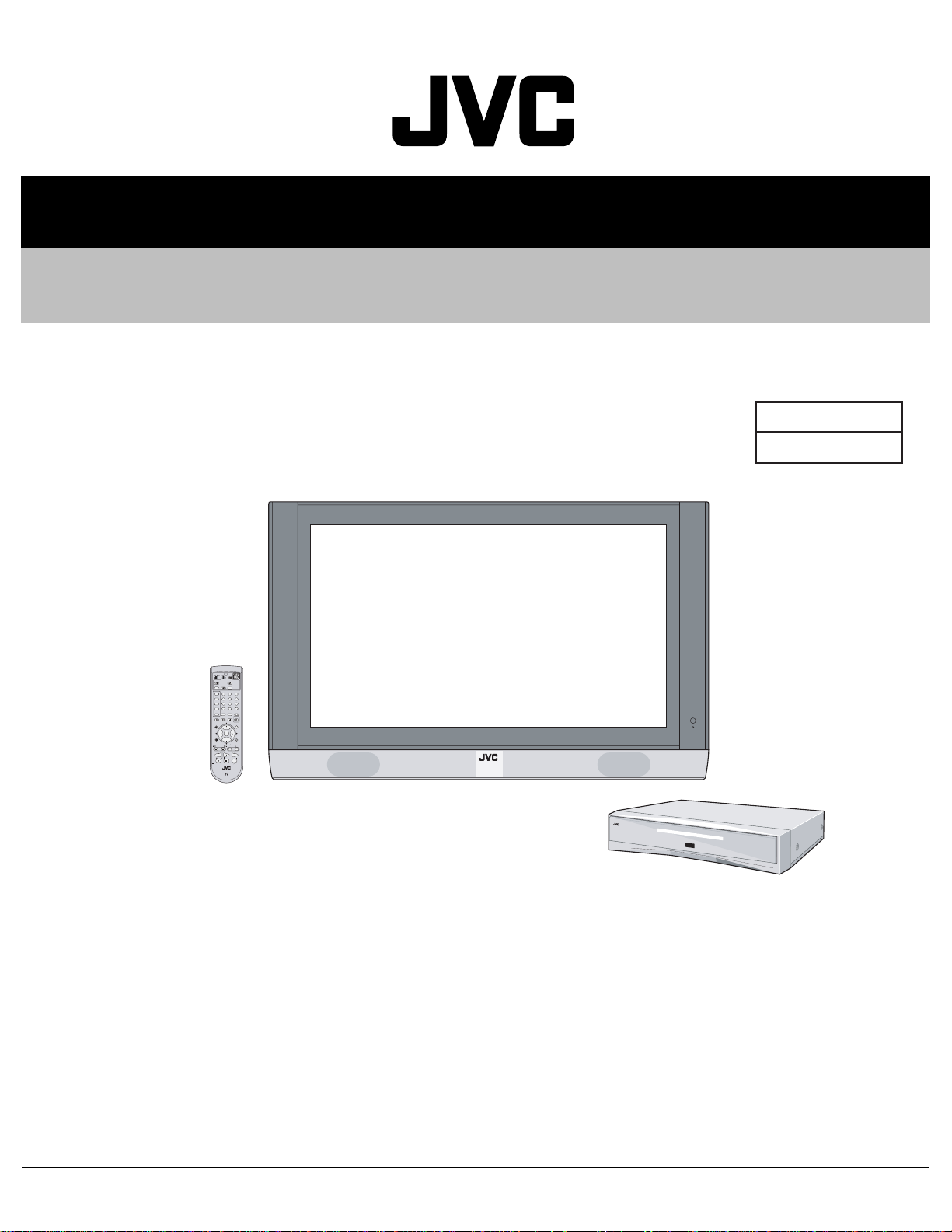
YA029200311
SERVICE MANUAL
PDP COLOR TELEVISION
PD-42WV74 /S
TV
CATV VCRDVD
ASPECT
MULTI SCREEN
INDEX
SPLIT
FREEZE
SWAP SELECT
INPUT 1
V1
123
INPUT 2
V2
456
INPUT 3
V3
789
RETURN+
INPUT 4
100+
TV
0
V4
THEATER
NATURAL
VIDEO
DIGITAL-IN
PRO
CINEMA
STATUS
D-IN
SLEEP TIMER
DISPLAY SOUND
LIGHT
+
MUTING
C.C.
C.C.
CH
VOL
VOL
OK
CH
MENU
BACK
VCR CHANNEL
VCR DVD
PREV NEXT
POWER
TV VCR
REW
FFPLAY
REC PAUSE
STOP
OPEN CLOSE
STILL PAUSE
RM-C13G
VM-42WV74
[PLASMA DISPLAY UNIT]
BASIC CHASSIS
SB3
TU-42WV74
[RECEIVER UNIT]
TABLE OF CONTENTS
1 PRECAUTION. . . . . . . . . . . . . . . . . . . . . . . . . . . . . . . . . . . . . . . . . . . . . . . . . . . . . . . . . . . . . . . . . . . . . . . . . 1-3
2 SPECIFIC SERVICE INSTRUCTIONS. . . . . . . . . . . . . . . . . . . . . . . . . . . . . . . . . . . . . . . . . . . . . . . . . . . . . . 1-6
3 DISASSEMBLY . . . . . . . . . . . . . . . . . . . . . . . . . . . . . . . . . . . . . . . . . . . . . . . . . . . . . . . . . . . . . . . . . . . . . . 1-10
4 ADJUSTMENTS . . . . . . . . . . . . . . . . . . . . . . . . . . . . . . . . . . . . . . . . . . . . . . . . . . . . . . . . . . . . . . . . . . . . . . 1-21
5 TROUBLESHOOTING . . . . . . . . . . . . . . . . . . . . . . . . . . . . . . . . . . . . . . . . . . . . . . . . . . . . . . . . . . . . . . . . . 1-55
COPYRIGHT © 2003 VICTOR COMPANY OF JAPAN, LIMITED
No.YA029
2003/11
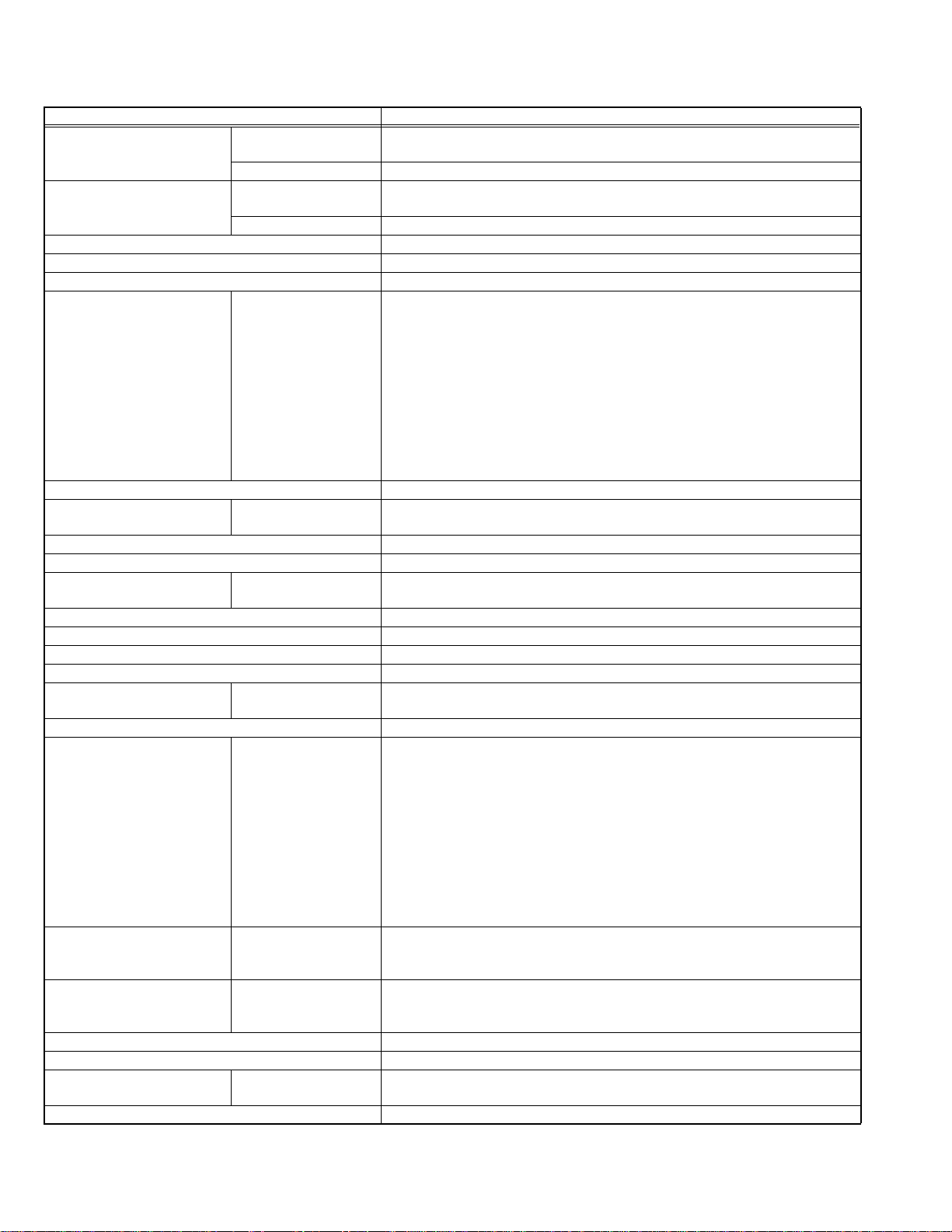
SPECIFICATION
Items Contents
Dimensions (W × H × D) Plasma display unit 116.0cm × 79.8cm × 30.8cm (45-11/16" × 31-7/16" × 12-3/16") [with the stand]
116.0cm × 73.1cm × 9.8cm (45-11/16" × 28-13/16" × 3-7/8") [main TV body]
Receiver unit 43.5cm × 9.9cm × 38.2cm (17-3/16" × 3-15/16" × 15-1/16")
Mass Plasma display unit 48kg (106lbs) [with the stand]
38kg (84lbs) [main TV body]
Receiver unit 5.1kg (11.3lbs)
TV RF System CCIR (M)
Color System NTSC
Sound System BTSC (Multi Channel Sound)
TV Receiving Channels and
Frequency
TV / CATV Total Channel 180 Channels
Intermediate Frequency Video IF
Color Sub Carrier 3.58 MHz
Power Input AC 120V, 60Hz
Power Consumption Plasma display unit
Plasma Display Panel (PDP) 42-inch wide aspect (16:9)
Screen Size Diagonal : 107.5cm (H:51.8cm × V : 105.7cm)
Display Pixels Horizontal : 852 dots × Vertica l : 480 dots (W-VGA)
Audio Power Output 18W + 18W (Main/Woofer)
Speaker Main
Antenna terminal (VHF/UHF) F-type connector, 75Ω unbalanced, coaxial
Video / Audio input
Input-1/2/3/4
Component Video
Digital-in Video
Audio output
Sub woofer output 0~1000mV (rms), Low impedance, RCA pin jack × 1
AV compulink III 3.5mm mini jack × 1
Display Input / Output
(For system cable)
Remote Control Unit RM-C13G (AA/R6 /U M-3 battery × 2)
Design & specifications are subject to change without notice.
VHF Low
VHF High
UHF
CATV
Sound IF
Receiver unit
Woofer
S-Video
[Input-1/2/4]
Video
Audio
[Input-1/2]
1125i / 750p
525p / 525i
Audio
Variable
Fix
Control / Audio
Video
02ch~06ch : 54MHz~88MHz
07ch~13ch : 174MHz~216MHz
14ch~69ch : 470MHz~806MHz
54MHz~804MHz
Low Band : 02~06, A-8 by 02~06&01
High Band : 07~13 by 07~13
Mid Band : A~I by 14~22
Super Band : J~W by 23~36
Hyper Band : W+1~W+28 by 37~64
Ultra Band : W+29~W+84 by 65~125
Sub Mid Band : A8, A4~A1 by 01, 96~99
45.75 MHz
41.25 MHz (4.5MHz)
340W
27W
10cm × 3cm (3-15/16" × 1-3/16"), oval type × 2
13cm × 6.5cm (5-1/8" × 2-9/16"), oval type × 2
Mini-DIN 4 pin × 3
Y: 1V (p-p), Positive (Negative sync provided), 75 Ω
C: 0.286V (p-p) (Burst signal), 75 Ω
1V (p-p), Positive (Negative sync provided), 75 Ω , RCA pin jack × 4
500mV (rms), High impedance, RCA pin jack × 8
RCA pin jack × 6
Y : 1V (p-p) (Sync signal: 0.35V(p-p), 3-value sync.), 75 Ω
Pb/Pr : 0.35V(p-p), 75 Ω
Y : 1V (p-p), Positive (Negative sync provided), 75 Ω
Pb/Pr : 0.35V(p-p), 75 Ω
DVI-D 24-pin connector × 1
(Digital-input terminal is not compatible with computer signal)
500mV (rms), Low impedance, RCA pin jack × 2
RCA pin jack × 2
More than 0 to 1000mV(rms) (+2.2 dBs)
500mV(rms) (-4dBs) Low impedance (400Hz when modulated 100%)
D-sub 26-pin connector × 2
DVI-D 24pin connector × 2
1-2 (No.YA029)
SECTION 1
PRECAUTION
1.1 SAFETY PRECAUTIONS
(1) The design of this product contains special hardware, many
circuits and components specially for safety purposes. For
continued protection, no changes should be made to the original
design unless authorized in writing by the manufacturer.
Replacement parts must be identical to those used in the original
circuits. Service should be performed by qualified personnel only.
(2) Alterations of the design or cir cuitry of the pr oducts shou ld n ot be
made. Any design alterations or additions will void the
manufacturer's warranty and will further relieve the manufacturer
of responsibility for personal injury or property damage resulting
therefrom.
(3) Many electrical and me chanical parts in the products have special
safety-related characteristics. These characteristics are often not
evident from visual inspection nor can the protection afforded by them
necessarily be obtained by using replacement components rated for
higher voltage, wattage, etc. Replacement parts w hich have these
special safety characteristics are identified in the parts list of Service
manual. Electrical components having such features are
identified by shading on the schematics and by ( ) on the
parts list in Service manual. The use of a substitute replacement
which does not have the same safety characteristics as the
recommended replacement part shown in the part s list of Service
manual may cause shock, fire, or other hazards.
(4) Use isolation transformer when hot chassis.
The chassis and any sub-chassis contained in some products are
connected to one side of the AC power line. An isolation
transformer of adequate capacity should be inserted between the
product and the AC power supply point while performing any
service on some products when the HOT chassis is exposed.
(5) Don't short between the LIVE side ground and ISOLATED (NEU-
TRAL) side ground or EARTH side ground when repairing.
Some model's power circuit is partly different in the GND. The difference of the GND is shown by the L IVE : ( ) side GND, the ISOLAT ED (NEUTRAL) : ( ) side GND and EARTH : ( ) side GND.
Don't short between the LIVE side GND and ISOLATED (NEUTRAL)
side GND or EARTH side GND and never measu re the LIVE side
GND and ISOLATED (NEUTRAL) side GND or EARTH side GND at
the same time with a measuring apparatus (oscilloscope etc.). If
above note will not be kept, a fuse or any parts will be broken.
(6) If any repair has been made to the chassis, it is recommended that
the B1 setting should be checked or adjusted (See B1 POWER
SUPPLY check).
(7) Do not check high voltage by drawing an arc. Use a high voltage
meter or a high voltage probe with a VTVM. Discharge the picture
tube before attempting meter connection, by connecting a clip lead
to the ground frame and connecting the other end of the lead
through a 10kΩ 2W resistor to the anode button.
(8) When service is required, observe the original lea d dress. Extra
precaution should be given to assure correct lead dress in the high
voltage circuit area. Where a short circuit has occurred, those
components that indicate evidence of overheating should be
replaced. Always use the manufacturer's replacement
components.
(9) Isolation Check (Safety for Electrical Shock Hazard)
After re-assembling the product, always perform an isolation
check on the exposed metal parts of the cabinet (antenna
terminals, video/audio input and output terminals, Control knobs,
metal cabinet, screw heads, earphone jack, control shafts, etc.) to
be sure the product is safe to operate without danger of electrical
shock.
a) Dielectric Strength Test
The isolation between the AC primary circuit and all metal parts
exposed to the user, particularly any exposed metal part having a
return path to the chassis should withstand a voltage of 1100V AC
(r.m.s.) for a period of one second.
(. . . . Withstand a voltage of 1100V AC (r.m.s.) to an appliance rat-
ed up to 120V, and 3000V AC (r.m.s.) to an appliance rated 200V
or more, for a period of one second.) This method of test requires
a test equipment not generally found in the service trade.
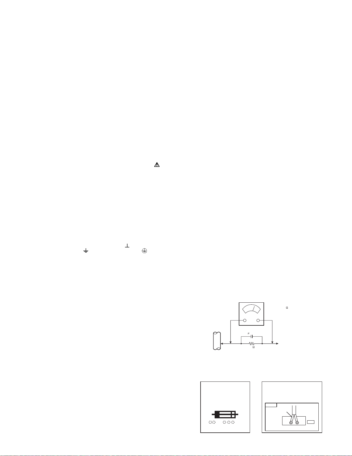
b) Leakage Current Check
Plug the AC line cord directly into the AC outlet (do not use a line
isolation transformer during this check.). Using a "Leakage
Current Tester", measure the leakage current from each exposed
metal part of the cabinet, particularly any exposed metal part
having a return path to the chassis, to a known good earth ground
(water pipe, etc.). Any leakage current must not exceed 0.5mA AC
(r.m.s.).
However, in tropical area, this must not exceed 0.2mA AC (r.m.s.).
Alternate Check Method
Plug the AC line cord directly into the AC outlet (do not use a
line isolation transformer during this check.). Use an AC
voltmeter having 1000Ω per volt or more sensitivity in the
following manner. Connect a 1500Ω 10W resistor paralleled by
a 0.15µF AC-type capacitor between an exposed metal part and
a known good earth ground (water pipe, etc.). Measure the AC
voltage across the resistor with the AC voltmeter. Move the
resistor connection to each exposed metal part, particularly any
exposed metal part having a return path to the chassis, and
measure the AC voltage across the resistor. Now, reverse the
plug in the AC outlet and repeat each measurement. Any
voltage measured must not exceed 0.75V AC (r.m.s.). This
corresponds to 0.5mA AC (r.m.s.).
However, in tropical area, this must not exceed 0.3V AC
(r.m.s.). This corresponds to 0.2mA AC (r.m.s.).
AC VOLTMETER
(HAVING 1000 /V,
OR MORE SENSITIVITY)
0.15 F AC-TYPE
PLACE THIS PROBE
1500 10W
GOOD EARTH GROUND
ON EACH EXPOSED
METAL PART
(10) High voltage hold down circuit check.
After repair of the high voltage hold down circuit, this circuit shall
be checked to operate correctly.See item "How to check the high
voltage hold down circuit".
This mark shows a fast
operating fuse, the
letters indicated below
show the rating.
A V
POWER CORD
REPLACEMENT WARNING.
Connecting the white line side of power
cord to "WHT" character side.
PWB
White line side
WHT
PW
(No.YA029)1-3
1.2 INSTALLATION
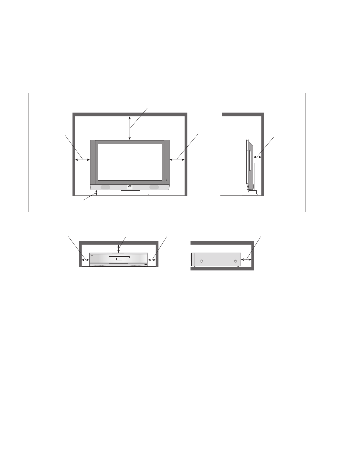
1.2.1 HEAT DISSIPATION
If the heat dissipation vent behind this unit is blocked, cooling
efficiency may deteriorate and temperature inside the unit will
rise. The temperature sensor that protects the unit will be
activated when internal temperature exceeds the pre-determined
level and power will be turned off automatically.Therefore,
please make sure pay attention not to block the heat dissipation
vent as well as the ventilation outlet behind the unit and ensu re
that there is room for ventilation around it.
SPACE REQUIRED FOR INSTALLATION OF THE DISPLAY UNIT
8 inch/200 mm
1.2.2 INSTALLATION REQUIREMENTS
Ensure that the minimal distance is maintained, as specified
below, between the unit with and the surrounding walls, as well
as the floor etc.Install the unit on stable flooring or stands.Ta ke
precautionary measures to prevent the unit from tipping in order
to protect against accidents and earthquakes.
6 inch/150 mm
2 inch/50 mm
SPACE REQUIRED FOR INSTALLATION OF THE RECEIVER UNIT
4 inch/100 mm
4 inch/100 mm4 inch/100 mm 4 inch/100 mm
6 inch/150 mm
2 inch/50 mm
1-4 (No.YA029)

1.3 HANDLING FOR PLASMA DISPLAY PANEL
1.3.1 PRECAUTIONS DURING NOTES FOR TRANSPORTATION
When transporting the display unit, pressure exerted on the
internal PDP (Plasma Display Panel) due to improper handling
(such as tossing and dropping) may cause damages even when
the unit is carefully packed. To prevent accidents from occurring
during transportation, pay careful attention prior to delivery such
as through explaining the handling instructions to transporters.
Ensure that the following requirements are met during
transportation, as the PDP of this unit is made of glass and
therefore fragile:
(1) Avoid vibrations and impacts
The unit may be broken if it is toppled sideways even when
properly packed. Ensure that the unit is carried by at lea st
2 persons and pay careful attention not to exert any
vibration or impact on it.
(2) Do not place equipment horizontallyEnsure that it is placed
upright and not horizontally during transportation and
storage as the PDP is very vulnerable to lateral impacts
and may break easily under such circumstances.During
transportation, ensure that the unit is loaded along the
traveling direction of travel of the vehicle, and avoid
stacking them on one another.For storage, ensure that
they are stacked in 2 layers or less even when placed
upright.
1.3.2 RESIDUAL IMAGE / BURN-IN ON SCREEN
Like CRTs, ‘burn-ins’ may occur when a same image is
continuously displayed over an extended period of time.As Tthis
may also shorten the life span of the PDP. Therefore, turn off the
display when not in use, scroll the screen, make use of screensavers, or allow even distribution on the display by inverting the
brightness, switching to complementary colors or inserting
animated images at periodic intervals.As burn-in is more likely to
occur with high brightness and contrast settings, try to use
neutral gradations or medium tone colors.Burn-in does not occur
in the case of animated images.When switching to another
image after continuous display of the previous image, residual
images may become prominent, as luminance in a part of the
display is higher than the other parts. This is not a defect b ut is
because due to the discharge surface of th e lighted porti on has
becomebeing relatively activated and its luminance higher than
the unlighted parts.
1.3.3 INFRARED RAYS
Near Near-infrared rays (800nm to 1000nm) are emitted from the
front of the panel, and this may give rise to glitchescause
malfunctions in infrared remote controls or communication
systems placed near it. In this case, avoid direct infrared rays
(and reflected rays in some cases) from the screen by either
changing the direction of the unit or other infrared systems or
securing a longer keeping a distance from the screen.
1.3.4 OPTICAL FILTER (PANEL FILTER)
Avoid placing the unit under direct sunlight over a prolonged
period of time. This may cause the optical filter to deteriorate in
quality and color.Clean the filter surface by wiping it softly lightly
with outing flannels a soft and lightly fuzz cloth (such as
flannel).Do not use solvents such as benzine or thinner to wipe
the filter surface. This may cause the filter to deteriorate in quality
or the coating on the surface to come off.As Tthe filter surface is
fragile., Ddo not scratch or hit it with hard materials.
1.3.5 NOTES PRECAUTIONS FOR REPLACEMENT OF
EXTERIOR PARTS
Take note of the following when replacing exterior parts (back
REAR COVER, FRONT PANEL, optical filter):Do not exert
pressure on the front of the PDP (glass surface).Pay careful
attention not to scratch or stain the front of the PDP (surface) with
hands.When replacing exterior parts, the front of the PDP should
be placed facing downward. Place a mat, etc. underneath to
avoid causing scratches to the front surface.However, never use
materials that are too soft (such as blanket cloth). If replacement
is made with the PDP surface facing downward and in contact
with the blanket, pressure may be exerted on the PDP, thus
causing damages to it.
(No.YA029)1-5

SECTION 2
SPECIFIC SERVICE INSTRUCTIONS
2.1 FEATURES
2.1.1 HIGH-DEFINITION IMAGE TECHNOLOGY (DIST)
DIST is a digital high-definition image processing technology that converts various image input signals such as NTSC(480i), 480p,
720p, and 1080i into a format with the best reso lution for a display device such as a plasma display panel, and displays highdefinition images.
2.1.2 MAIN FUNCTION
AUTO POWER OFF
The power supply of the TV will be cut off automatically when there is a continuous absence of signal for 4 minutes, or when there
is a maximum of 3 consecutive hours of no operation from user.
OFF TIMER
Setting for situations such as falling asleep while watch ing TV , and for preventio n against forgetti ng to turn off the TV. The power
supply of the TV will be cut off automatically when the time exceeds the set up timing (maximum 2 hours).
NATURAL CINEMA
When viewing film-originated movie and animation, misty outline can be seen in fast moving image s. Using natural cinema will
enable viewing of clear images even in fast moving images.
2.1.3 ASPECT CONTROL
SCREEN SIZE SWITCHING
Desired screen size (PANORAMA / CINEMA / FULL / HD PANORAMA / REGULAR / CINEMA ZOOM) can be selected.
MOVING THE SCREEN UP & DOWN
Adjusts the vertical position of the screen.
2.1.4 MULTI-SCREEN FUNCTION
SPLIT-SCREEN
2 programs an be viewed at the same time.
INDEX-SCREEN
This allows you to quickly look at to 12channels at a time so that you can decide which one to watch.
FREEZE SCREEN
The images that are currently seen can be viewed on the memo screen (still picture).
It is convenient for taking down notes like application address and recipe of cooking program etc, while enjoying the current program.
1-6 (No.YA029)

2.2 TECHNICAL INFORMATION
2.2.1 PDP (PLASMA DISPLAY PANEL) DESCRIPTION
2.2.1.1 CAUTION
Although a PDP is made with highly advanced precision, this does not necessarily mean all of the cells operate correctly.
The PDP inevitably includes cell that do not light or light constantly.
If the specifications (PDP performance) are unclear at the time of shipment, an adequate description cannot be conveyed to the
customer. In event of inquiries from customers regarding PDP performance, check the followi ng specifications in order to offer a
suitable reply.
2.2.1.2 CELL ARRANGEMENT
The PDP is constructed of front and rear glass substrates provided wit h respective discharge electrodes. Between these, neon for
discharging and xenon for generating ultraviolet rays are enclosed.
One picture element (pixel) is composed of Red, Green and Blue (RGB) cells. The cell p itch is 0.365mm horizontal (1.095mm per
pixel) by 1.110mm vertical.
As shown in Fig. 1, the cells are arranged for each R / G / B colour. A pixel consists of each cell of R/G/B/ colour. The size of a cell is
0.365mm horizontally and 1.110mm vertically.
Direction
Vertical(V)
Horizontal(H)
1st pixel
line
2nd pixel
line
479th pixel
line
480th pixel
line
1st pixel
array
B G R B G R
BG
G RBG R
B
GRBGR
B
H 1.095mm
Pitch of pixel
2nd pixel
array
RBG R
One pixel
(1dot)
B cell
G cell
R cell
851th pixel
array
B GRBG R
BGRBGR
G RBG R
B
GRBGR
B
852th pixel
array
H 0.365mm
Pitch of cell
V 1.110mm
Pitch of pixel
(Pitch of cell)
Fig.1 PIXEL (CELL) ARRANGEMENT
2.2.1.3 PIXEL FAULT
There are three pixel faults - bright fault , dark fault and flicker fault - that are respectively defined as follows.
(1) BRIGHT FAULT
In this pixel fault, a cell that should not light originally is lighting on and off.
For checking this pixel fault, input ALL BLACK SCREEN and find out the cell that is lighting on and off.
(2) DARK FAULT
In this pixel fault, a cell that should light originally is not lighting or lighting with the brightness twice as brighter as originally lighting.
For checking this pixel fault, input 100% of each R/G/B colour and find out the cell that is not lighting.
(3) FLICKER FAULT
In the pixel fault, a cell that should light originally or not light originally is flashing on and off.
For checking this pixel fault, input ALL BLACK SCREEN signal or 100% of each RGB colour and find out the cell that is flashing on
and off.
(No.YA029)1-7
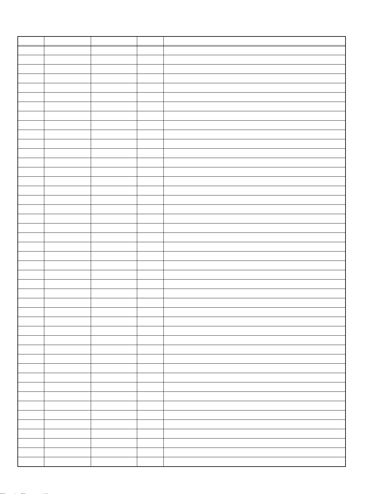
2.2.2 MAIN MI-COM FUNCTIONAL TABLE [RECEIVER UNIT]
Pin No. Terminal name Port name I/O Function
1 BS-RxD SBO0 O PDP communication
2 /MICON_V /VSYNC I Vertical sync for OSD
3 LB_PRO P84 I Low B protection detect [Detection : H]
4 NC NC - Not used
5 /RST /RST I Reset for CPU [Reset : L]
6 CONV.BUSY P52 IRQ4 I Not used
7 /TEST /TEST I 3.3V
8 OSD_YS YS O OSD Ys
9 /DPCRST P83 O Not used
10 BS/D P50 O Not used
11 A_MU P82 O Audio muting [Muting: H]
12 /MICON_H /HSYNC I Horizontal sync for OSD
13 M_MU P81 O Not used
14 P46.OSDXI P46 OSDXI - Not used
15 P45.OSDXO P45 OSDXO - Not used
16 SDA2 P44 I/O Not used
17 AC_IN TM5IOB I AC power supply (60Hz)
18 SCL2 P42 O Not used
19 TU_POW P41 O Tuner power control [ON : L]
20 VCOI VCOI I LPF input
21 PDO PDO O LPF output
22 /IP_RESET P80 O Reset (L) [Reset : L]
23 OSD_YM DAYMOUT O OSD YM
24 OSD_B DABOUT O OSD B
25 POW_LED P77 O Lighting for power [Lighting : H]
26 OSD_G DAGOUT O OSD G
27 OSD_R DAROUT O OSD R
28 VREF VREF I Not used
29 IP_ERR P76 I AMDP program load
30 IREF IREF I Not used
31 COMP COMP I Not used
32 AVDD AVDD I 3.3V
33 CLL CLL O Not used
34 VREFLS VREFLS I Standard voltage (For SUB CCD)
35 SUB_CCD CVBS1 I Not used
36 NC NC - Not used
37 VSS VSS I GND
38 MAIN_CCD CVBS0 I Not used
39 VREFHS VREFHS I Standard voltage (For MAIN CCD)
40 CLH CLH I Not used
41 VDD/VPP VDD(VPP) I 3.3V
42 CLKSW1 P75 O IP clock switch [ON : L]
43 CLKSW2 P74 O IP clock switch [ON : L]
44 ON_TIM P27 O Not used
45 PDP-Rx SBO1 O PDP communication
1-8 (No.YA029)

Pin No. Terminal name Port name I/O Function
46 PDP-Tx P25 SBD1 I PDP communication
47 SBT1 SBT1 I Port for writing on board
48 NC P23 I Not used
49 NC P22 O Not used
50 SRQ P21 O Not used
51 BS1.5CTL P20 O Not used
52 /DVI_RST PWM2 O Not used
53 DVI_HP PWM1 O DVI Connection detect [Connect : H]
54 /MDR_CON PWM0 O Panel connection detect [Connect : L]
55 /BS_POW P73 O Not used
56 BS_CLK_SEL P14 O Not used
57 TU2_AID ADIN8 I Not used
58 /LOB_POW P72 O LOW B power control
59 /COMPULINK /IRQ3 I Not used
60 /POWERGOOD /IRQ2 I Power condition check [ON : L]
61 MECHA_SW P10/IRQ1 I Discontinuation of mechanical swtich detection [Pussing : L]
62 /MAIN_POW P71 O Main power control [ON : L]
63 NC NC - Not used
64 /B1_POW P70 O Not used
65 C/N ADIN4 I Not used
66 X_RAY ADIN3 I Not used
67 EE_CDS ADIN2 I Not used
68 KEY2 ADIN1 I Key scan data [ON : H]
69 KEY1 ADIN0 I Key scan data [ON : H]
2
70 SCL1 SCL1 O I
71 SDA1 SDA1 I/O I
C bus clock (For Main memory)
2
C bus data (For Main memory)
72 REMO RMIN/IRQ0 I Remote control data
73 NC P87 O Not used
74 VSS VSS I GND
75 OSC2 OSC2 O 4MHz oscillation for system clock
76 OSC1 OSC1 I 4MHz oscillation for system clock
77 VDD VDD I 3.3V
2
78 SCL0 SCL0 O I
C bus clock (for general)
79 NC P86 O Not used
2
80 SDA0 SDA0 I/O I
81 DVI_SDA P57SBT0 O I
C bus data (for general)
2
C bus data (for digital input)
82 NC P56SBD0 I Not used
83 NC NC - Not used
84 P_MU P85 O Picture muting [Muting : H]
(No.YA029)1-9

SECTION 3
DISASSEMBLY
3.1 DISASSEMBLY PROCEDURE (DISPLLAY UNIT)
• Prior to assembly/disassembly procedure of the set, be sure to
disconnect the power cord from the wall outlet.
• Perform the following procedures on a flat and strong place.
3.1.1 REMOVING THE REAR COVER (Fig.1)
(1) Remove the 9 screws [ A ] .
(2) Remove the 12 screws [ B ].
(3) Take out the REAR COVER.
B
SIDE SPEAKER
COVER
H
SHIELD COVER
3.1.2 REMOVING THE SIDE SPEAKER COVER (Fig.1)
(1) Remove the 4 screws [ C ].
(2) Take out the SIDE SPEAKER COVER.
(3) Remove the other hand SIDE SPEAKER COVER same
steps.
A
REAR COVER
I
J
C
TERMINAL
BRACKET
DISPLAY SW PWB
X
T
C
E
DISPLAY SW
ASS'Y
SIDE SPEAKER
COVER
TOP
D
MAIN
SPEAKER
ASS'Y
Fig.2
DISPLAY LED PWB
G
F
1-10 (No.YA029)
Fig.1
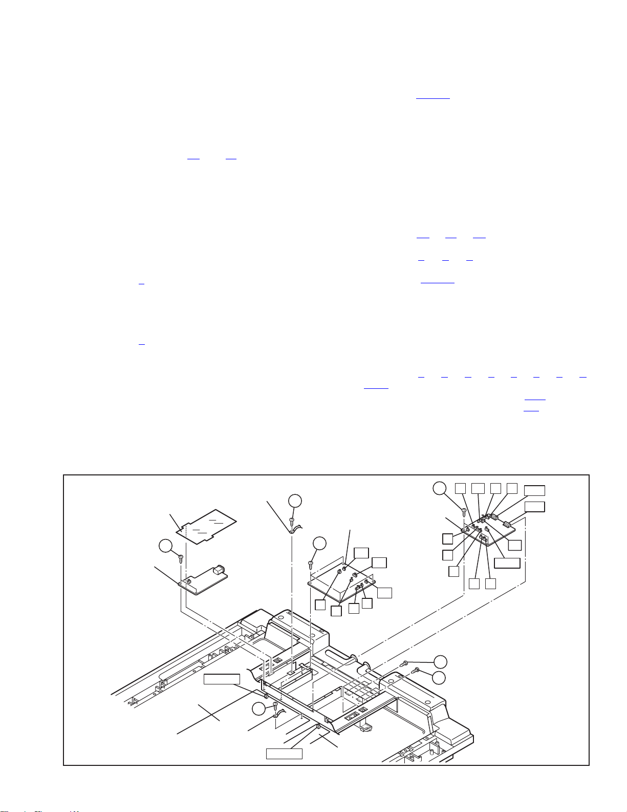
3.1.3 REMOVING THE MAIN SPEAKER ASS'Y (Fig.1, Fig.2)
NOTE:
Please do not disassembly MAIN SPEAKER ASS'Y. A
performance may be influenced if it disassembly.
• Remove the SIDE SPEAKER COVER.
(1) Remove the 2 screws [ D ].
(2) Take out the MAIN SPEAKER ASS'Y.
(3) Remove the other hand MAIN SPEAKER ASS'Y same
steps.
(4) If necessary, remove the [SR
] and [SL] connector.
3.1.4 REMOVING THE DISPLAY SW ASS'Y (Fig.1)
• Remove the SIDE SPEAKER COVER.
(1) Remove the 2 screws [ E ].
(2) Take out the DISPLAY SW ASS'Y.
3.1.5 REMOVING THE DISPLAY SW PWB (Fig.1)
• Remove the SIDE SPEAKER COVER.
• Remove the DISPLAY SW ASS'Y.
(1) Remove the 3 screws [ F ].
(2) Take out the DISPLAY SW PWB.
(3) Remove the [ T
] connector on the DISPLAY SW PWB.
3.1.6 REMOVING THE SENSOR PWB (Fig.1)
• Remove the SIDE SPEAKER COVER.
(1) Remove the 2 screws [ G ].
(2) Take out the SENSOR PWB.
(3) Remove the [ X
] connector on the SENSOR PWB.
3.1.7 REMOVING THE SHIELD COVER (Fig.1)
• Remove the REAR COVER.
(1) Remove the 6 screws [ H ].
(2) Take out the SHIELD COVER.
3.1.8 REMOVING THE TERMINAL BRACKET (Fig.1)
• Remove the REAR COVER.
• Remove the SHIELD COVER.
(1) Remove the 5 screws [ I ].
(2) Remove the 2 screws [ J ].
(3) Take out the TERMINAL BRACKET.
3.1.9 REMOVING THE LINE FILTER PWB (Fig.2)
• Remove the REAR COVER.
• Remove the SHIELD COVER.
• Remove the TERMINAL BRACKET.
(1) Remove the [ CN8001
] ( AC IN ) connector on the SMPS
PWB.
(2) Remove the 1 screw [ K ] attaching the earth wire ( black )
on the PDP UNIT.
(3) Remove the 1 screw [ L ] attachin g the earth wire ( green
and yellow ).
(4) Remove the 2 screws [ M ] .
(5) Take out the LINE FILTER PWB.
3.1.10 REMOVING THE AUDIO PWB (Fig.2)
• Remove the REAR COVER.
• Remove the SHIELD COVER.
• Remove the TERMINAL BRACKET.
(1) Remove the [ SR
], [ SL ], [ CB ] connector on the AUDIO
PWB.
(2) Remove the [ A
], [ C ], [ D ] connector on the DISPLAY
INTERFACE PWB.
(3) Remove the [ CN9003
] ( B ) connector on the VIDEO
SMPS PWB.
(4) Remove the 4 screws [ N ].
(5) Take out the AUDIO PWB.
3.1.11 REMOVING THE DISPLAY INTERFACE PWB (Fig.2)
• Remove the REAR COVER.
• Remove the SHIELD COVER.
• Remove the TERMINAL BRACKET.
(1) Remove the [ A
], [ C ], [ D ], [ E ], [ T ], [ X ], [ V ], [ G ],
[ LVDS ] connector on the DISPLAY INTERFACE PWB.
(2) Remove the 2 screws [ O ] attaching the MDR connector.
(3) Remove the 2 screws [ P ] attaching the DVI
connector.
(4) Remove the 2 screws [ Q ].
(5) Take out the DISPLAY INTERFACE PWB.
INSULATOR
LINE FILTER
PWB
M
SMPS PWB
EARTH WIRE
(GREEN &YELLOW)
CN8001
K
EARTH
WIRE
(BLACK)
CN9003
L
AUDIO PWB
N
B
A
VIDEO SMPS PWB
Fig.2
Q
V D
C2
DISPLAY
INTERFACE
PWB
A
SL
CB
SR
D
C
X
T
O
P
GE
LVDS
C
C1
MDR
DVI
(No.YA029)1-11
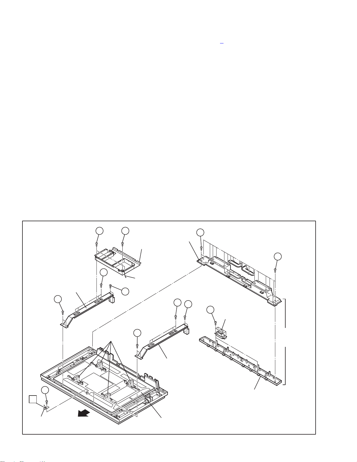
3.1.12 REMOVING THE CHASSIS BASE (Fig.3)
• Remove the REAR COVER.
• Remove the SHIELD COVER.
• Remove the TERMINAL BRACKET.
• Remove the LINE FILTER PWB.
• Remove the AUDIO PWB.
• Remove the DISPLAY INTERFACE PWB.
(1) Remove the 2 screws [ R ].
(2) Remove the 1 screw [ S ] attaching the earth wire.
(3) If necessary, remove the cable and wires from wire clamp.
(4) Pull up the CHASSIS BASE.
3.1.13 REMOVING THE BACK FRAME BRACKET (Fig.3)
• Remove the REAR COVER.
• Remove the SHIELD COVER.
• Remove the TERMINAL BRACKET.
• Remove the LINE FILTER PWB.
• Remove the AUDIO PWB.
• Remove the DISPLAY INTERFACE PWB.
• Remove the CHASSIS BASE.
(1) Remove the 4 screws [ T ].
(2) Remove the 4 screws [ U ].
(3) If necessary, remove the cable and wires from wire clamp.
(4) Pull up the BACK FRAME BRACKET.
(5) The other hand BACK FRAME BRACKET is removed
same steps.
3.1.14 REMOVING THE TEMP. SENSOR PWB (Fig.3)
• Remove the REAR COVER.
(1) Remove the [ V
] connector on the TEMP. SENSOR PWB.
(2) Remove the screw [ V ].
(3) Take out the TEMP. SENSOR PWB.
3.1.15 REMOVING THE PDP UNIT (Fig.3)
• Remove the REAR COVER.
• Remove the SHIELD COVER.
• Remove the TERMINAL BRACKET.
• Remove the LINE FILTER PWB.
• Remove the AUDIO PWB.
• Remove the DISPLAY INTERFACE PWB.
• Remove the CHASSIS BASE.
• Remove the BACK FRAME BRACKET.
• Remove the TEMP. SENSOR PWB.
(1) Rise with the back frame spacer on the PDP UNIT back
side.
(2) Take out the PDP UNIT.
3.1.16 REMOVING THE WOOFER SPEAKER BOX (Fig.3)
(1) Remove the 6 screws [ W ].
(2) Take out the WOOFER SPEAKER BOX.
3.1.17 REMOVING THE SPEAKER (WOOFER) (Fig.3)
• Remove the WOOFER SPEAKER BOX.
(1) Remove the 20 screws [ X ].
(2) Pull up the WOOFER SPEAKER HOLDER.
(3) Remove the 4 screws [ Y ].
(4) Take out the WOOFER.
(5) Remove the other hand WOOFER same steps.
R
U
BACK FRAME
BRACKET
T
BACK FRAME
SPACER
V
V
S
CHASSIS BASE
EARTH
WIRE
T
T
WOOFER
SPEAKER
HOLDER
U
BACK FRAME
BRACKET
W
X
T
Y
SPEAKER
(WOOFER )
WOOFER
SPEAKER
BOX
WOOFER SPEAKER
BACK COVER
TEMP. SENSOR
PWB
1-12 (No.YA029)
TOP
PDP UNIT
Fig.3

3.1.18 THE SIDE BLACKET (Fig.4)
• Remove the REAR COVER.
• Remove the SHIELD COVER.
• Remove the TERMINAL BRACKET.
• Remove the LINE FILTER PWB.
• Remove the AUDIO PWB.
• Remove the DISPLAY INTERFACE PWB.
• Remove the CHASSIS BASE.
• Remove the BACK FRAME BRACKET.
• Remove the PDP UNIT.
(1) Remove the 2 screws [ Z ].
(2) Remove the screw [ a ].
(3) Remove the screw [ b ] attaching the earth wire.
(4) Pull up the SIDE BRACKET.
(5) Remove the other hand SIDE BRACKET same steps.
Z
a
3.1.19 REMOVE THE FRONT FILTER (Fig.4)
• Remove the REAR COVER.
• Remove the SHIELD COVER.
• Remove the TERMINAL BRACKET.
• Remove the LINE FILTER PWB.
• Remove the AUDIO PWB.
• Remove the DISPLAY INTERFACE PWB.
• Remove the CHASSIS BASE.
• Remove the BACK FRAME BRACKET.
• Remove the PDP UNIT.
(1) Remove the 2 screws [ c ] attaching the UPPER
BRACKET.
(2) Remove the 6 screws [ d ] attaching the GLASS HOLDER
(UPPER) from upper side.
(3) Pull up the UPPER BRACKET.
(4) Remove the 2 screws [ e ] attaching the UPPER
BRACKET.
(5) Remove the 6 screws [ f ] attaching the GLASS HOLDER
(UPPER) from under side.
(6) Take out the FRONT FILTER .
PDP UNIT
SIDE BRACKET
MOUNTING
BOSS
UPPER
BRACKET
GLASS HOLDER
(UPPER)
TOP
GLASS HOLDER
(UNDER)
e
UNDER
BRACKET
c
EARTH
WIRE
a
d
FRONT PANEL
SIDE BRACKET
f
Z
b
Fig.4
FRONT FILTER
(No.YA029)1-13

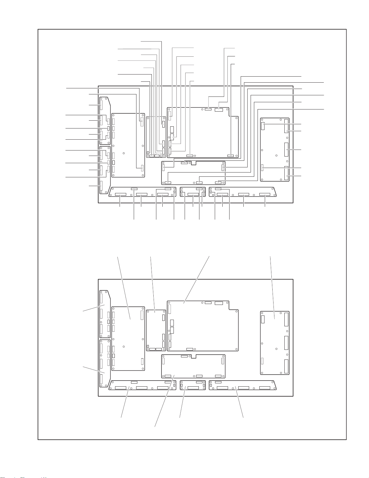
3.1.20 DISASSEMBLY PDP UNIT
3.1.20.1 REMOVING THE SMPS PWB
• Remove the REAR COVER.
(1) Remove the CN8007
CN8009
(2) Remove the 8 screws [g].
(3) Remove the SMPS PWB.
3.1.20.2 REMOVING THE X-MAIN PWB
• Removing the REAR COVER.
(1) Remove the CN4001
connectors on the X-MAIN PWB.
(2) Remove the 8 screws [h].
(3) Remove the X-MAIN PWB.
3.1.20.3 REMOVING THE Y-BUF-U PWB
• Remove the REAR COVER.
(1) Remove the CN5401
connectors on the Y-BUF-U PWB.
(2) Remove the 5 screws [I].
(3) Lift the Y-BUF-U PWB slightly, and remove th e CN5404
CN5405 connectors on the Y-BUF-U PWB.
(4) Remove the Y-BUF-U PWB.
3.1.20.4 REMOVING THE Y-BUF-L PWB
• Remove the REAR COVER.
(1) Remove the CN5501
connectors on the Y-BUF-L PWB.
(2) Remove the 5 screws [j].
(3) Lift the Y-BUF-L PWB slightly, and remove the CN5504/
CN5505
(4) Remove the Y-BUF-L PWB.
3.1.20.5 REMOVING THE Y-MAIN PWB
• Remove the REAR COVER.
• Remove the CHASSIS BASE.
• Remove the Y-BUF-U PWB.
• Remove the Y-BUF-L PWB.
(1) Remove the CN5001
PWB.
(2) Remove the 7 screws [k].
(3) Remove the Y-MAIN PWB.
/CN8002 connectors on the SMPS PWB.
connectors on the Y-BUF-L PWB.
/CN8008/CN8004/BUFFER/CN8003/
/CN4002/CN4003/CN4004/CN4005
/CN5402/CN5403/CN5406
/CN5502/CN5503/CN5506
/CN5008 connectors on the Y-MAIN
3.1.20.6 REMOVING THE LOGIC-MAIN PWB
• Remove the REAR COVER.
• Remove the CHASSIS BASE.
(1) Remove the CN101
connectors on the LOGIC-MAIN PWB.
(2) Remove the 6 screws [l].
(3) Remove the LOGIC-MAIN PWB.
3.1.20.7 REMOVING THE E-BUF PWB
• Remove the REAR COVER.
• Remove the BACK FRAME.
• Remove the CHASSIS BASE.
• Remove the SPEAKER BRACKET (left).
(1) Remove the EC1
connectors on the E-BUF PWB.
(2) Remove the 6 screws [m].
(3) Remove the E-BUF PWB.
3.1.20.8 REMOVING THE F-BUF PWB
/
• Remove the REAR COVER.
• Remove the BACK FRAME.
• Remove the CHASSIS BASE.
(1) Remove the FC4
BUF PWB.
(2) Remove thr 4 screws [n].
(3) Remove the F-BUF PWB.
3.1.20.9 REMOVING THE G-BUF PWB
• Remove the REAR COVER.
• Remove the BACK FRAME.
• Remove the CHASSIS BASE.
• Remove the SPEAKER BRACKET (right).
(1) Remove the GC5
the G-BUF PWB.
(2) Remove the 6 screws [o].
(3) Remove the G-BUF PWB.
3.1.20.10 REMOVING THE VIDEO SMPS PWB
• Remove the REAR COVER.
(1) Remove the CN9001
CN9007
(2) Remove the 4 screws [p].
(3) Remove the VIDEO SMPS PWB.
connectors on the VIDEO SMPS PWB.
/CN201/CN401/CN402/CN403/CN803
/EC2/EC3/CN401/CN806/EF1
/CN402/FE1/FG1 connectors on the F-
/GC6/GC7/CN403/GF1 connectors on
/CN9002/CN9004/CN9005/CN9006/
1-14 (No.YA029)
CN5008
CN5404
CN5406
CN5405
CN5505
CN5506
CN5504
CN5001
CN5401
CN5402
CN5403
CN5501
CN5502
CN5503
CN9007
CN9003
CN9001
CN9005
CN9006
CN9002
CN9004
CN8003
BUFFER
CN8004
CN8007
CN8008
CN8009
CN8002
CN8001
CN201
CN803
CN101
CN401
CN402
CN403
CN4001
CN4003
CN4004
CN4002
CN4005
Y-BUF-U PWB
Y-BUF-L PWB
EC1
Y-MAIN PWB
EC2 EC3
CN806 CN401 CN402 CN403
EF1
FC4 FC4
FE1
GC5 GC6 GC7
GF1
SMPS PWBVIDEO SMPS PWB
X-MAIN PWB
E-BUF PWB G-BUF PWBF-BUF PWB
LOGIC-MAIN PWB
Fig.5
(No.YA029)1-15
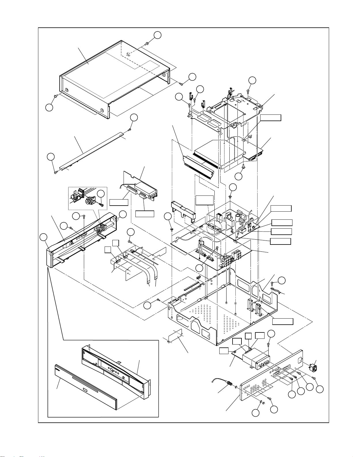
3.2 DISASSEMBLY PROCEDURE (RECEIVER UNIT) (Fig. 6)
• Make sure that the power cord is pulled out from the AC wall
socket.
3.2.1 REMOVING THE TOP COVER
(1) Remove the 4 screws [ A ] from both side of the TOP
COVER.
(2) Remove the 3 screws [ B ] from rear side of the TOP
COVER.
(3) Pull up the TOP COVER.
3.2.2 REMOVING THE BACK COVER
• Remove the TOP COVER.
(1) Remove the 2 screws [ C ] attaching the AC connector.
(2) Remove the 3 screws [ D ].
(3) Remove the 6 screws [ E ] attaching the each jacks.
(4) Remove the 2 screws [ F ] attaching the digital connector.
(5) Remove the 2 screws [ G ] attaching the DIGITAL INPUT
MODULE.
(6) Remove the 2 screws [ H ] attaching the DVI terminal.
(7) Remove the 1 nat [ I ] attaching the antenna terminal.
(8) Take out the rear cover.
3.2.3 REMOVING THE CHASSIS BRACKET
• Remove the TOP COVER.
(1) Remove the 2 screws [ J ].
(2) Pull up the CHASSIS BRACKET.
3.2.4 REMOVING THE DIGITAL INPUT MODULE
• Remove the TOP COVER.
• Remove the BACK COVER.
(1) Remove the connector [ AU
], [ SR ], [ DC ], [ Q ] on the
DIGITAL INPUT MODULE.
(2) Remove the 2 screws [ K ].
(3) Take out the DIGITAL INPUT MODULE.
3.2.5 REMOVI NG THE MI-COM & DIST MODULE PWB AN D
DIST RELAY PWB
• Remove the TOP COVER.
• Remove the BACK COVER.
• Remove the DIGITAL INPUT MODULE.
(1) Remove the [ CN100A
] connector on the MI-COM & DIST
MODULE PWB.
(2) Remove the 2 screws [ L ].
(3) Remove the 2 screws [ M ].
(4) Remove the 2 screws [ N ].
(5) Pull up the DIST RELAY PWB from MAIN PWB.
(6) Remove the 5 screws [ O ] attaching the MI-COM & DIST
MODULE PWB.
(7) Take out the MI-COM & DIST MODULE PWB and DIST
RELAY PWB from the DIST HOLDER.
3.2.6 REMOVING THE RECEIVER POWER PWB
• Remove the TOP COVER.
• Remove the BACK COVER.
• Remove the DIGITAL INPUT MODULE.
• Remove the MI-COM & DIST MODULE PWB and DIST
RELAY PWB.
(1) Remove the [ CN1001
] and [ CN1002 ] connector on the
MAIN PWB.
(2) Remove the [ CN90PW
] [ CN900X ] and [ CN90E1 ]
connector on the RECEIVER POWER PWB.
(3) Remove the earth wire [ CN90E2 ] from chassis.
(4) Remove the 6 screws [ P ].
(5) Take out the RECEIVER POWER PWB.
3.2.7 REMOVING THE FRONT PANEL
• Remove the TOP COVER.
(1) Remove the 1 screw [ Q ] from front side.
(2) Remove the 1 screw [ R ] from top side.
(3) Remove the 2 claws [ Y ] from left and right side.
(4) Pull out the FRONT PANEL.
3.2.8 REMOVING THE DAMPER
• Remove the TOP COVER.
• Remove the FRONT PANEL.
(1) Remove the 1 screw [ S ] from back side of the FRONT PANEL.
(2) Remove the DAMPER.
3.2.9 REMOVING THE FRONT CONTROL PWB
• Remove the TOP COVER.
• Remove the FRONT PANEL.
(1) Remove the card wire from the [ H
] and [ G ] connector.
(2) Remove the 4 screws [ T ].
(3) Take out the FRONT CONTROL PWB.
3.2.10 REMOVING THE RECEIVER PWB
• Remove the TOP COVER.
• Remove the BACK COVER.
• Remove the CHASSIS BRACKET.
• Remove the DIGITAL INPUT MODULE.
• Remove the MI-COM & DIST MODULE PWB and DIST RELAY PWB.
(1) Remove the [ CN1005
] and [ CN1006 ] connector.
(2) Pull up the RECEIVER PWB.
3.2.11 REMOVING THE MAIN PWB
• Remove the TOP COVER.
• Remove the BACK COVER.
• Remove the CHASSIS BRACKET.
• Remove the DIGITAL INPUT MODULE.
• Remove the MI-COM & DIST MODULE PWB and DIST RELAY PWB.
• Remove the FRONT PANEL.
• Remove the RECEIVER PWB.
(1) Remove the 3 screws [ U ] attaching the bracket.
(2) Remove the 2 screws [ V ].
(3) Remove the 2 screws [ W ].
(4) Take out the MAIN PWB.
DIGITAL INPUT MODULE
BACK COVER
1-16 (No.YA029)
1
3
5
SB
connector
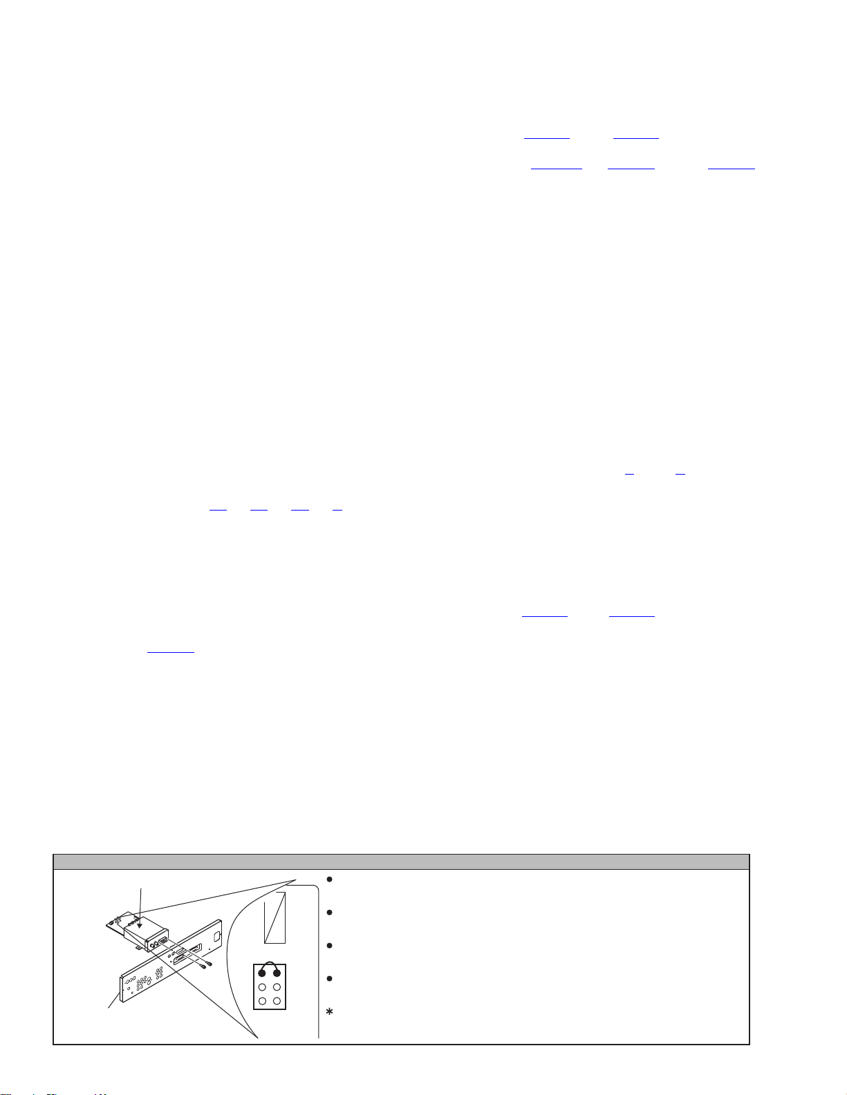
CAUTION AT DISASSEMBLY
Prior to disassembly, unplug the power code from the AC outlet without fail. (Turn
the power "off".)
Short the SB connector [1] pin and [2] pin of the DIGITAL INPUT MODULE. (At the
time of assembling)
Before the rear panel is inserted into the cabinet, release the short-circuit between
2
4
6
the SB connector [1] pin and [2] pin of the DIGITAL INPUT MODULE.
After releasing the short-circuit between the SB connectors, do not turn the power
on until the rear panel is inserted into the cabinet.
Negligence in carrying out the above steps may cause the inactivation of the TV.
TOP COVER
A
(x4)
A
CHASSIS BRACKET
J
(x2)
FRONT
PANEL
Y
Claw
a
FRONT PANEL
(BACK SIDE)
DAMPER
R
(x1)
Q
B
(x3)
M
N
(x2)
J
(x2)
L
(x2)
DIST HOLDER
CN100A
DIST RELAY PWB
b
MI-COM & DIST
MODULE PWB
RECEIVER PWB
O
(x5)
S
c
CN1006
Y
Claw
H
T
(x4)
CN1005
(x2)
CN1001
CN1002
V
G
P
(x6)
RECEIVER POWER PWB
g
CN90PW
CN90E1
CN90E2
CN900X
MAIN PWB
FRONT
DOOR
FRONT
CONTROL
PWB
FFC WIRE
U
(x2)
FRONT PANEL
e
e
d
BRACKET
Fig.6
(x2)
d
a
ANTENNA
TERMINAL
W
DC
AU
DIGITAL INPUT
MODULE PWB
c
BACK COVER
BOTTOM CASE
b
C
g
SR
Q
EARTH WIRE
CN90E2
K
(x2)
AC
INLET
F
(x2)
D
(x3)
G
H
(x2)
(x2)
I
E
(x6)
(No.YA029)1-17

3.3 REPLACEMENT OF MEMORY IC
MAIN MENU
This unit uses the nonvolatile memory IC. The memory IC memories data for video-chroma and drive circuits. To replace the memory
IC without the data written, malfunctions might occurred while power is on, and the normal image might not appear. Wh en replaci ng
the memory IC, be sure to use the IC written with the initial values of data.
3.3.1 PROCEDURE FOR REPLACING THE MEMORY IC
NOTE:
Before entering the SERVICE MODE, confirm that the setting
of TV / CATV SW of the REMOTE CONTROL UNIT is at the
"TV" side and the setting of VCR / DVD SW is at the "VCR"
side. If the switches have not been properly set, you cannot
enter the SERVICE MODE.
(1) Switch the power off and unplug the power cord from the
wall outlet.
(2) Replacing the memory IC. [Be sure to use the IC written
with the initial values of data]
(3) Plug the power cord into the wall outlet and switch the
power on.
(4) Receive channel setting
(5) User setting
Memories the user setting items. The [SETTINGS OF
FACTORY SHIPMENT] setting is as next page.
(6) SERVICE MODE
Check the SERVICE MODE setting items of setting mode
in Table 1, set if necessary. For setting method, please
refer to the [ADJUSTMENT PREPARATION :
ADJUSTMENT PROCEDURE ] of ADJUSTMENT section.
MAIN MENU
1.PICTURE/SOUND
2.YC SEP
3.WHITE BALANCE
4.MEMORY SETUP
7.PANEL
8.PP
9.IP
0.HDMI
5.RF AFC
6.DD/CM
1. PICTURE/SOUND (sound and picture setting)
Sound circuits (A) Fixed A01~A27
Video circuits (S) Adjust S01~S99
Deflection circuits (D) Fixed D01~D32
Factory setting items (F) Adjust F01~F59
2. YC SEP
3-dimensional YC separation
setting
3. WHITE BALANCE: Cannot adjust
4. MEMORY SETUP: Do not adjust
Memory data edit Fixed -
5. RF AFC: AFC setting (Automaticaly set)
6. DD/CM
Panel image processing setting Adjust DDT01~DDT34
7. PANEL: Do not adjust
Panel power limit control Fixed PDA001~PDA012
8. PP
Multi-screen processing setting A djust ADM001~ADM034
9. IP
DIST processing setting Fixed IPA001~IPA120
0. HDMI
Digital input process setting Fixed HDM001~HDM080
SERVICE MODE SETTING ITEMS
Setting items Settings Item No.
Adjust YCM001~YCM185
Fixed YCS001~YCS114
Fixed CMT01~CMT57
Fixed DDP01~DDP37
Fixed CMP01~CMP03
Fixed PDB001~PDA021
Fixed RGA001~RGA003
Fixed PPA001~PPA008
Fixed PPB001~PPB036
Fixed PPC001~PPC008
Fixed PPD001~PPD025
Fixed IPB001~IPB079
Fixed IPC001~IPC044
Fixed IPD001~IPD026
Fixed IPE001~IPE015
Fixed RHD001~RHD170
1-18 (No.YA029)
 Loading...