

Page 1
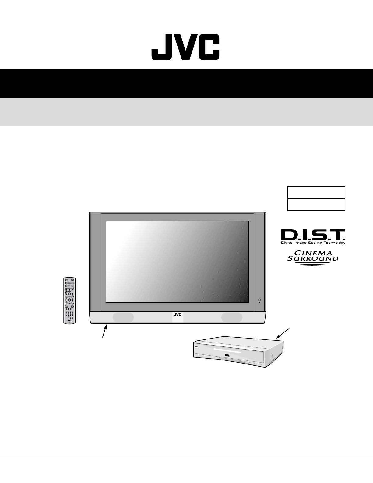
SERVICE MANUAL
PDP COLOUR TELEVISION
PD-42DV2
PD-42DV2/S
BASIC CHASSIS
MK
VM-42DV2
VM-42DV2/S
[PLASMA DISPLAY UNIT]
1 PRECAUTION
2 SPECIFIC SERVICE INSTRUCTIONS
3 DISASSEMBLY
4 ADJUSTMENT
5 TROUBLESHOOTING
......................................................................................................................................................... 1-3
....................................................................................................................................................... 1-9
...................................................................................................................................................... 1-22
........................................................................................................................................... 1-48
COPYRIGHT © 2003 VICTOR COMPANY OF JAPAN, LTD.
TU-42DV2
TU-42DV2/S
[RECEIVER UNIT]
TABLE OF CONTENTS
...................................................................................................................... 1-6
No.YA018
2003/11
Page 2
SPECIFICATION
Items Contents
Dimensions (W x H x D) Plasma display unit
Receiver unit 43.5cm x 9.9cm x 38.2cm
Mass Plasma display unit 38.0kg
Receiver unit 5.6kg
TV RF System B, G, I, D, K, M
Colour System TV Mode PAL / SECAM/NTSC3.58/NTSC4.43
Video Mode PAL / SECAM / NTSC3.58 / NTSC4.43
Stereo System A2 (B/G, D/K), NICAM (B/G, I, D/K)
Teletext System FLOF (Fastext), TOP, WST (World Standard System)
Receiving Frequency VHF Low 46.25MHz ~ 168.25MHz
UHF High 175.25MHz ~ 463.25MHz
Intermediate Frequency VIF 38.0MHz (B, G, I, D, K, L)
Colour Sub Carrier Frequency
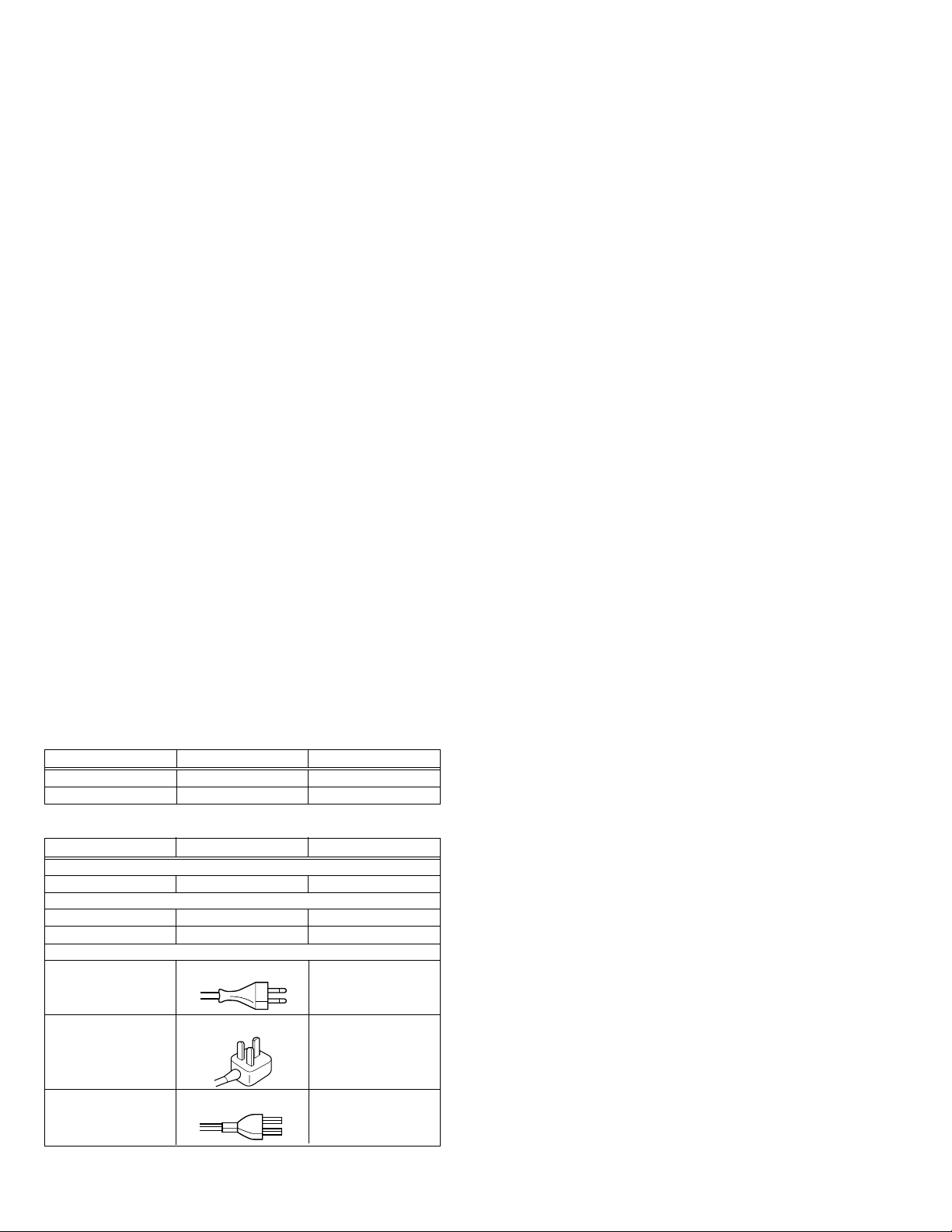
Power Input AC110V ~ AC240V, 50Hz / 60Hz
Power Consumption Plasma display unit Operate : 330W, Stand by: 1.5W
Receiver unit Operate : 30W, Stand by: 2.4W
Plasma Display Panel (PDP) ! QLE0023-002
Screen Size Visible size : 107.5cm (Diagonel) / 93.4cm x 53.4cm (H x V)
Display Pixels Horizontal: 852 pixels / Vertical: 480 pixels [W-VGA]
Speaker Main : 3cm x 10cm, Oval type x2
Audio Power Output Main : 9W + 9W
Aerial Input Teminal 75Ω unbalanced
Video / Audio Iutput S-Video (2/3/5) Mini-DIN 4 pin connector x3
(1/2/3/4/5) Y : 1V(p-p), positive (negative sync provided), 75
Video (1/2/3/5) 1V(p-p), negative sync, 75Ω, RCA pin jacj x4
Audio (1/2/3/4/5) 500mV(rms) (-4dBs), high impedance, RCA pin jack x10
Component (4) RCA pin jack x3
Video / Audio Output Video 1V(p-p), 75Ω, RCA pin jack x1
Audio
Headphone 3.5mm stereo mini jack x1
Display Input / Output Terminal Control / Audio: 26-pin D-sub connector
(For system cable) Video: 24pin DVI-D connector
Remote Control Unit RM-C1808 (AA/R6 battery x 2)
116.0cm x 73.1cm x 9.8cm
UHF 471.25MHz ~ 863.25MHz
CATV Mid: X~Z, S11~S10
Super: S11~S20
Hyper: S21~S41
32.26MHz (5.74MHz: B), 32.15MHz (5.85MHz: G), 31.45MHz (6.55MHz: I)
SIF
31.75MHz (6.25MHz: D), 32.15MHz (5.85MHz: K)
PAL : 4.43MHz
SECAM : 4.40MHz / 4.25MHz
NTSC : 3.58MHz / 4.43MHz
42-inch wide aspect (16:9)
Woofer : 6.5cm x 13cm, Oval type x2
Woofer : 9W + 9W
Ω
C: 0.286V(p-p) (Burst signal), 75
Y : 1V(p-p), positive (negative sync), 75
CB/CR : 0.7V(p-p), 75
500mV(rms)(-4dBs), Low impedance (400Hz when modulated 100%),
RCA pin jack x4
Ω
Ω
Ω
Design & specifications are subject to change without notice.
1-2 (No.YA018)
Page 3

D
SECTION 1
PRECAUTION
1. 1 SAFETY PRECAUTIONS
(1) The design of this product contains special hardware,
many circuits and components specially for safety
purposes. For continued protection, no changes should
be made to the original design unless authorized in writing
by the manufacturer. Replacement parts must be identical
to those used in the original circuits. Service should be
performed by qualified personnel only.
(2) Alterations of the design or circuitry of the products should
not be made. Any design alterations or additions will void
the manufacturer's warranty and will further relieve the
manufacturer of responsibility for personal injury or
property damage resulting therefrom.
(3) Many electrical and mechanical parts in the products have
special safety-related characteristics. These
characteristics are often not evident from visual inspection
nor can the protection afforded by them necessarily be
obtained by using replacement components rated for
higher voltage, wattage, etc. Replacement parts which
have these special safety characteristics are identified in
the parts list of Service manual. Electrical components
having such features are identified by shading on the
schematics and by (!) on the parts list in Service
manual. The use of a substitute replacement which does
not have the same safety characteristics as the
recommended replacement part shown in the parts list
of Service manual may cause shock, fire, or other hazards.
(4) Don't short between the LIVE side ground and ISOLATED
(NEUTRAL) side ground or EARTH side ground when
repairing.
Some model's power circuit is partly different in the GND.
The difference of the GND is shown by the LIVE : (
GND, the ISOLATED (NEUTRAL) : (
EARTH : (
) side GND. Don't short between the LIVE
) side GND and
side GND and ISOLATED (NEUTRAL) side GND or EARTH
side GND and never measure the LIVE side GND and
ISOLATED (NEUTRAL) side GND or EARTH side GND at
the same time with a measuring apparatus (oscilloscope
etc.).If above note will not be kept, a fuse or any parts will
be broken.
(5) If any repair has been made to the chassis, it is
recommended that the B1 setting should be checked or
adjusted (See ADJUSTMENT OF B1 POWER SUPPLY).
(6) The high voltage applied to the picture tube must conform
with that specified in Service manual. Excessive high
voltage can cause an increase in X-Ray emission, arcing
and possible component damage, therefore operation
under excessive high voltage conditions should be kept
to a minimum, or should be prevented. If severe arcing
occurs, remove the AC power immediately and determine
the cause by visual inspection (incorrect installation,
cracked or melted high voltage harness, poor soldering,
etc.). To maintain the proper minimum level of soft X-Ray
emission, components in the high voltage circuitry
including the picture tube must be the exact replacements
or alternatives approved by the manufacturer of the
complete product.
(7) Do not check high voltage by drawing an arc. Use a high
voltage meter or a high voltage probe with a VTVM.
Discharge the picture tube before attempting meter
connection, by connecting a clip lead to the ground frame
and connecting the other end of the lead through a 10kΩ
2W resistor to the anode button.
) side
(8) When service is required, observe the original lead dress.
Extra precaution should be given to assure correct lead
dress in the high voltage circuit area. Where a short circuit
has occurred, those components that indicate evidence
of overheating should be replaced. Always use the
manufacturer's replacement components.
(9) Isolation Check
(Safety for Electrical Shock Hazard)
After re-assembling the product, always perform an
isolation check on the exposed metal parts of the cabinet
(antenna terminals, video/audio input and output
terminals, Control knobs, metal cabinet, screw heads,
earphone jack, control shafts, etc.) to be sure the product
is safe to operate without danger of electrical shock.
a) Dielectric Strength Test
The isolation between the AC primary circuit and all metal
parts exposed to the user, particularly any exposed metal
part having a return path to the chassis should withstand
a voltage of 3000V AC (r.m.s.) for a period of one second.
(. . . . Withstand a voltage of 1100V AC (r.m.s.) to an
appliance rated up to 120V, and 3000V AC (r.m.s.) to an
appliance rated 200V or more, for a period of one second.)
This method of test requires a test equipment not generally
found in the service trade.
b) Leakage Current Check
Plug the AC line cord directly into the AC outlet (do not use
a line isolation transformer during this check.). Using a
"Leakage Current Tester", measure the leakage current
from each exposed metal part of the cabinet, particularly
any exposed metal part having a return path to the chassis,
to a known good earth ground (water pipe, etc.). Any
leakage current must not exceed 0.5mA AC (r.m.s.).
However, in tropical area, this must not exceed 0.2mA AC
(r.m.s.).
Alternate Check Method
Plug the AC line cord directly into the AC outlet (do not
use a line isolation transformer during this check.).
Use an AC voltmeter having 1000 ohms per volt or
more sensitivity in the following manner. Connect a
1500Ω 10W resistor paralleled by a 0.15µF AC-type
capacitor between an exposed metal part and a known
good earth ground (water pipe, etc.). Measure the AC
voltage across the resistor with the AC voltmeter. Move
the resistor connection to each exposed metal part,
particularly any exposed metal part having a return path
to the chassis, and measure the AC voltage across
the resistor. Now, reverse the plug in the AC outlet and
repeat each measurement. Any voltage measured
must not exceed 0.75V AC (r.m.s.). This corresponds
to 0.5mA AC (r.m.s.).
However, in tropical area, this must not exceed 0.3V AC
(r.m.s.). This corresponds to 0.2mA AC (r.m.s.).
AC VOLTMETER
(HAVING 1000Ω/V,
OR MORE SENSITIVITY)
0.15µF AC-TYPE
PLACE THIS PROBE
1500Ω 10W
GOOD EARTH GROUND
ON EACH EXPOSE
ME TAL PAR T
(No.YA018) 1-3
Page 4
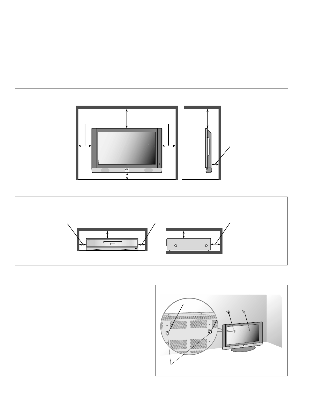
1.2 INSTALLATION
1.2.1 HEAT DISSIPATION
If the heat dissipation vent behind this unit is blocked, cooling
efficiency may deteriorate and temperature inside the unit will
rise. The temperature sensor that protects the unit will be
activated when internal temperature exceeds the predetermined level and power will be turned off automatically.
Therefore, please make sure pay attention not to block the heat
dissipation vent as well as the ventilation outlet behind the unit
and ensure that there is room for ventilation around it.
SPACE REQUIRED FOR INSTALLATION OF THE DISPLAY UNIT
1.2.2 INSTALLATION REQUIREMENTS
Ensure that the minimal distance is maintained, as specified
below, between the unit with and the surrounding walls, as well
as the floor etc.
Install the unit on stable flooring or stands.
Take precautionary measures to prevent the unit from tipping in
order to protect against accidents and earthquakes.
150 mm or
more
200 mm or
more
150 mm
or more
50 mm or more
SPACE REQUIRED FOR INSTALLATION OF THE RECEIVER UNIT
100 mm or more
100 mm or more
100 mm or more
200 mm
or more
50 mm or more
100 mm or more
100 mm or more
1.2.3 FALL TIP PREVENTION MEASURES
Take precautionary measures to prevent the unit from falling or
tipping to protect against emergencies such as earthquakes as
well as accidents.
Fasten the supplied hook for tip fall prevention using the screws,
also supplied, behind the display unit, and use them together
with durable cords (to be purchased separately) to secure the
unit to a robust part such as the wall surface or pillars.
1-4 (No.YA018)
The supplied hook for tipfall prevention
Page 5

1. 3 PRECAUTIONS REGARDING PDP
1.3.1 PRECAUTIONS DURING NOTES FOR TRANSPORTATION
When transporting the display unit, pressure exerted on the
internal PDP (Pplasma Ddisplay Ppanel) due to improper
handling (such as tossing and dropping) may cause damages
even when the unit is carefully packed. To prevent accidents
from occurring during transportation, pay careful attention prior
to delivery such as through explaining the handling instructions
to transporters.
Ensure that the following requirements are met during
transportation, as the PDP of this unit is made of glass and
therefore fragile:
(1) Avoid vibrations and impacts
The unit may be broken if it is toppled sideways even
when properly packed. Ensure that the unit is carried by at
least 2 persons and pay careful attention not to exert any
vibration or impact on it.
(2) Do not place equipment horizontally
Ensure that it is placed upright and not horizontally during
transportation and storage as the PDP is very vulnerable
to lateral impacts and may break easily under such
circumstances.
During transportation, ensure that the unit is loaded along
the traveling direction of travel of the vehicle, and avoid
stacking them on one another.
For storage, ensure that they are stacked in 2 layers or
less even when placed upright.
1.3.4 OPTICAL FILER (PANEL FILTER)
Avoid placing the unit under direct sunlight over a prolonged
period of time. This may cause the optical filter to deteriorate in
quality and color.
Clean the filter surface by wiping it softly lightly with outing flannels
a soft and lightly fuzz cloth (such as flannel).
Do not use solvents such as benzine or thinner to wipe the filter
surface. This may cause the filter to deteriorate in quality or the
coating on the surface to come off.
As Tthe filter surface is fragile., Ddo not scratch or hit it with hard
materials.
1.3.5 NOTES PRECAUTIONS FOR REPLACEMENT OF
EXTERIOR PARTS
Take note of the following when replacing exterior parts (back
REAR COVER, FRONT PANEL, optical filter)
• Do not exert pressure on the front of the PDP (glass surface).
• Pay careful attention not to scratch or stain the front of the PDP
(surface) with hands.
• When replacing exterior parts, the front of the PDP should be
placed facing downward. Place a mat, etc. underneath to avoid
causing scratches to the front surface. However, never use
materials that are too soft (such as blanket cloth). If
replacement is made with the PDP surface facing downward
and in contact with the blanket, pressure may be exerted on
the PDP, thus causing damages to it.
1.3.2 RESIDUAL IMAGE / BURN-IN ON SCREEN
Like CRTs, "burn-in" may occur when a same image is
continuously displayed over an extended period of time.
As Tthis may also shorten the life span of the PDP. Therefore,
turn off the display when not in use, scroll the screen, make use
of screen-savers, or allow even distribution on the display by
inverting the brightness, switching to complementary colors or
inserting animated images at periodic intervals.
As burn-in is more likely to occur with high brightness and contrast
settings, try to use neutral gradations or medium tone colors.
Burn-in does not occur in the case of animated images.
When switching to another image after continuous display of
the previous image, residual images may become prominent,
as luminance in a part of the display is higher than the other
parts.
This is not a defect but is because due to the discharge surface
of the lighted portion has becomebeing relatively activated and
its luminance higher than the unlighted parts.
1.3.3 INFRARED RAYS
Near Near-infrared rays (800nm to 1000nm) are emitted from
the front of the panel, and this may give rise to glitchescause
malfunctions in infrared remote controls or communication
systems placed near it. In this case, avoid direct infrared rays
(and reflected rays in some cases) from the screen by either
changing the direction of the unit or other infrared systems or
securing a longer keeping a distance from the screen.
(No.YA018) 1-5
Page 6
SECTION 2
SPECIFIC SERVICE INSTRUCTIONS
2.1 FEATURES
2.1.1 HIGH-DEFINITION IMAGE TECHNOLOGY (DIST)
• DIST (Digital Image Scaling Technology)
Employs an interpolation method that doubles the scanning
lines to realize 480-line flickerfree picture making it especially
suitable for reproducing high-resolution pictures even on largescreen displays.
2.1.2 MAIN FUNCTION
•
DIGITAL VNR
The DIGITAL VNR function cuts down the amount of noise in
original picture. There are three function settings of AUTO,MIN
and MAX.
• Super DigiPure
This function uses the latest technology to give viewer a natural
looking picture.
It consist of DigiPure and picture motion compensation function.
•
MOVIE THEATRE
This function displays a cinema film picture more smoothly
and naturally on the screen.
•
COLOUR MANAGEMENT
This function ensures dull colours are compensated to produce
natural hues.
• Sleep Timer
Setting for situations such as falling asleep while watching TV,
and for prevention against forgetting to turn off the TV. The
power supply of the TV will be cut off automatically when the
time exceeds the set up timing (maximum 2 hours).
• 3D SOUND function
This function makes the speaker sounds like in a wider
ambience.
• Teletext function
The teletext broadcast can be viewed and the teletext pages
can be stored in memory.
• T-V LINK function
This function make a VCR could automatically download the
data or image from the TV, and turn on the TV to view the image
when it playing.
2.1.3 ASPECT CONTROL
The screen size can be changed according to the picture aspect
ratio.
• ZOOM function
Desired screen size (AUTO/REGULAR / PANORAMIC / 14:9
ZOOM / 16:9 ZOOM / 16:9 ZOOM SUBTITLE / FULL) can be
selected.
2.1.4 MULTI-SCREEN FUNCTION
• Twin-pictures / PIP function
With the function, two pictures can be displayed at the same
time (Twin pictures mode and Picture in picture mode).
• Multi-picture function
With this function, one of multi-picture (12 pictures) can be
displayed at the same time.
• Freeze function
The images that are currently seen can be viewed on the memo
screen (still picture).
It is convenient for taking down notes like application address
and recipe of cooking program etc, while enjoying the current
program.
2.2 UNIT COMPOSITION
MODEL DISPLAY UNIT RECEIVER UNIT
PD-42DV2 VM-42DV2 TU-42DV2
PD-42DV2/S VM-42DV2/S TU-42DV2/S
2. 3 MAIN DIFFERENCE LIST
Item PD-42DV2 PD-42DV2/S
DISPLAY unit
FRONT FILTER LC32461-001A LC32436-001A
RECEIVER unit
RATING LABEL LC21209-003B-0L LC21209-004B-0L
BACK COVER LC21211-003A LC21211-004A
ACCESSORY
QMPL050-250-K
POWER CORD(EU)
QMPP170-200-JC
POWER CORD(EK)
QMPB320-180-R
POWER CORD(JP)
---
←
---
1-6 (No.YA018)
Page 7
2. 4 TECHNICAL INFORMATION
2.4.1 PDP STRUCTURE AND CHARACTERISTIC
This unit (Display Unit) uses the flat type panel PDP (Plasma Display Panel), instead of the conventional CRT (Cathode Ray Tube),
as a display unit.
2.4.1.1 PIXEL (CELL) ARRAY
PDP is constructed by sealing the xenon, which emits neon and ultraviolet rays for discharging purpose, in between the electrodes
lay on the front glass substrate and rear glass substrate.
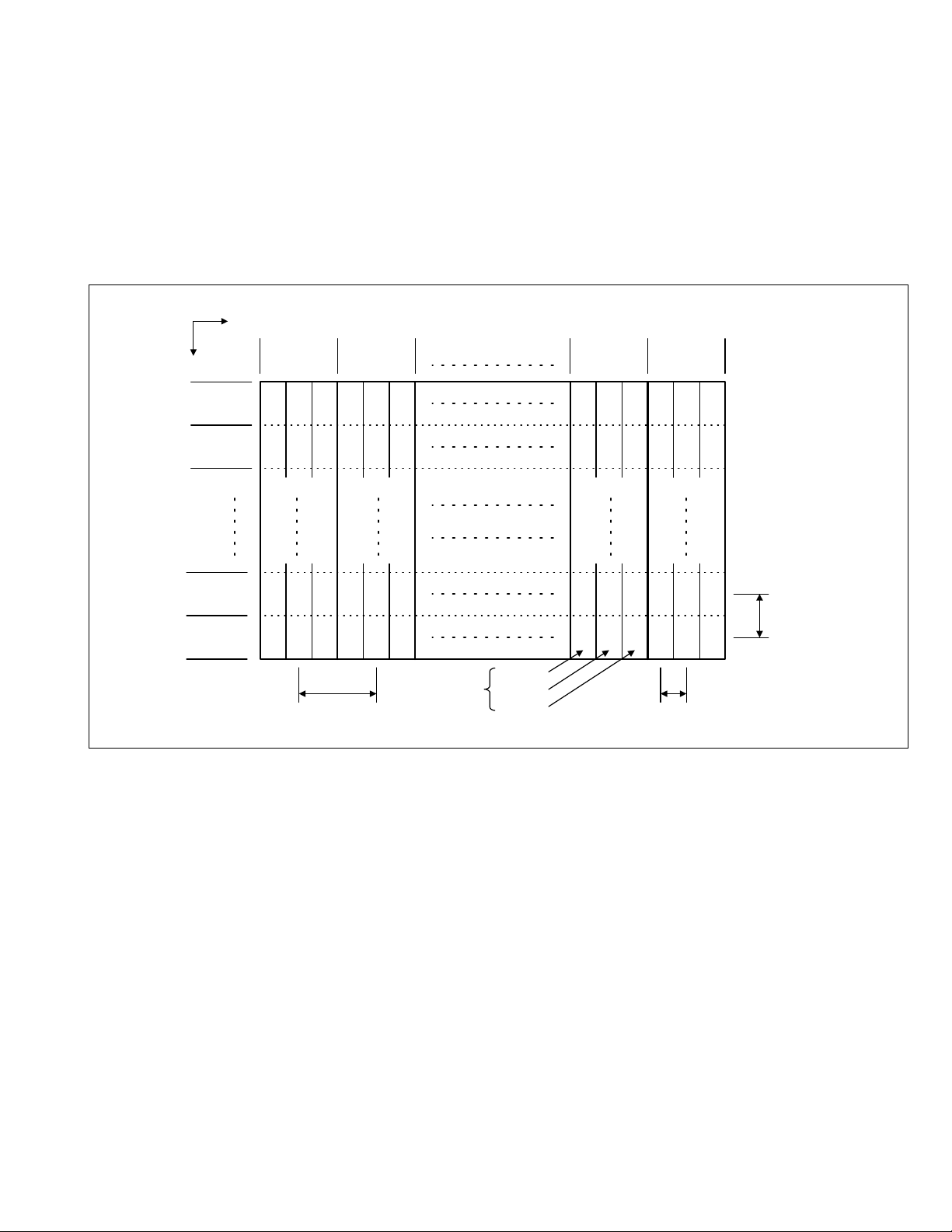
One pixel is composed of 3 RGB cells, with cell pitch of 0.365mm (1 pixel 1.095mm) horizontally and 1.110mm vertically.
The cell is arrayed in each RGB color as shown in Fig. 1. One pixel is formed by interlacing each RGB color cell.
One cell size is 0.365mm horizontally and 1.110mm vertically.
Direction
Vertically
No.1
Pixel line
No.2
Pixel line
No.479
Pixel line
No.480
Pixel line
Horizontally
No.1
Pixel
sequence
B G R B G R
BG
B
B
1.095mm(Horizontally)
RBGR
G RBG R
GRBGR
Pixel pitch
No.2
Pixel
sequence
1 pixel
(1 dot)
B Cell
G
Cell
R Cell
No.851
Pixel
sequence
No.852
Pixel
sequence
B GRBG R
BGRBGR
G RBG R
B
GRBGR
B
0.365mm(Horizontally)
Cell pitch
1.110mm
(Vertically)
Pixel pitch
(Cell pitch)
Fig.1
2.4.1.2 PIXEL DEFECTS
Though PDP is made by means of ultra precise technology, there are cases whereby not all pixels (cell) will function properly. In
some cases, there may be defective pixels that do not light at all or the ones that always light on.
There are 3 types of Pixel defects, [Bright Dot Defects], [Dark Dot Defects] and [Flicker Dot Defects], as defined respectively in the
following:
(1) Bright Dot Defects
Bright dot defect is a pixel cell that lights though it should not light.
The presence of bright dot defects can be confirmed by inputting a full black signal (pattern).
(2) Dark Dot Defects
Dark dot defect is a pixel cell that does not light, though it should light.
The presence of dark dot defects can be confirmed by inputting a 100% full white signal (pattern).
(3) Flicker Dot Defects
Flicker dot defect is a pixel cell that blinks though it should light or not light.
The presence of flicher dot defects can be confirmed by inputting a full black signal (pattern).
(No.YA018) 1-7
Page 8
2.4.2 MAIN CPU FUNCTIONAL TABLE (RECEIVER UNIT)
Pin No. Terminal Name Port Name I/O Remark
1
TCK
2
TMS
3
TDI
4
TDO
5
REMOCON
6
KEY1
7
KEY2
8
KEY3
9
TV_LINK
10
POWER
11
PROTECT
12
POWERG
13
VSS33
14
VDD33
15
TV_LINK OUT
16
A20
17
A19
18
A18
19
A17
20
VSS25
21
VDD25
22
A16
23
A8
24
A7
25
A9
26
A6
27
A5
28
A10
29
A11
30
A12
31
VSS33
32
VDD33
33
A4
34
A3
35
A2
36
A1
37
A0
38
A13
39
A14
40
A15
41
VSS33
42
VDD33
43
CLK
44
CSSDRAM
45
CKE
46
CSROM
47
RD
48
UDQM
49
LDQM
50
WR
51
D15
52
VSS33
53
VDD33
54
D7
55
D0
56
D14
57
D8
58
D6
59
D1
60
VSS33
61
VDD33
62
D13
63
D9
64
D5
TCK
TMS
TDI
TDO
P2.8
P2.9
P2.10 (NOR/INST)
P2.11
P2.12
P2.13
P2.14
P2.15
VSS33
VDD33
P4.5
A20
A19
A18
A17
VSS25
VDD25
A16
A8
A7
A9
A6
A5
A10
A11
A12
VSS33
VDD33
A4
A3
A2
A1
A0
A13
RAS/A14
CAS/A15
VSS33
VDD33
MEMCLK
CSSDRAM
CLKEN
CSROM
RD
UDQM
LDQM
WR
D15
VSS33
VDD33
D7
D0
D14
D8
D6
D1
VSS33
VDD33
D13
D9
D5
O
I/O
I/O
I/O
I/O
I/O
I/O
I/O
I/O
O
O
O
O
O
O
O
O
O
O
O
O
O
O
O
O
O
O
O
O
O
O
O
O
O
O
O
O
O
O
I/O
I/O
I/O
I/O
I/O
I/O
I/O
I/O
I/O
I/O
I
I
I
I
GND
I
3.3V
I
GND
I
2.5V
I
GND
I
3.3V
I
GND
I
3.3V
I
GND
I
3.3V
I
GND
I
3.3V
Pin No. Terminal Name Port Name I/O Remark
65
66
67
68
69
70
71
72
73
74
75
76
77
78
79
80
81
82
83
84
85
86
87
88
89
90
91
92
93
94
95
96
97
98
99
100
101
102
103
104
105
106
107
108
109
110
111
112
113
114
115
116
117
118
119
120
121
122
123
124
125
126
127
128
D2
D12
D10
VSS33
VDD33
D4
D3
D11
RESET-IN
SCL0
SDA0
PIX_CLK
AMP_MUTE
AUDIO_MUTE
READY
STATUS
DATA
CLK
VSS33
VDD33
VSS25
VDD25
TXD0
RXD0
IE-MUTE
AA_SDA
AA_SCL
YS2
HP_DET
NC
NC
IIC_FREE
SCL1
SCA1
MSP_RESET
SDA2
VSYNC
HSYNC
NC
YS
VDD33
VSS33
XTAL1
XTAL2
VSSA
VSSD
R
G
B
VSSA
VSSD
CVBS2A
VSSA
VDDA
CVBS1B
CVBS1A
VSSA
VDDA
AFC1
AFC2
AGC
KEYP2
TMODE
D2
D12
D10
VSS33
VDD33
D4
D3
D11
RSTIN
P3.0
P3.1
P3.2
P3.3
P3.4
P3.5
P3.6
P3.7
P3.8
P3.9
VSS33
VDD33
VSS25
VDD25
TXD0
RXD0
P3.12
P3.13
P3.15
P5.14(YS2)
P5.15
TRIG_IN
TRIG_OUT
P6.2
P6.3
P6.4
P6.5
P6.6
VSYNC
HSYNC
COR/RSTOUT
BLANK
VDD33
VSS33
XTAL1
XTAL2
VSSA
VDDA
R
G
B
VSSA
VDDA
CVBS2
VSSA
VDDA
CVBS1B
CVBS1A
VSSA
VDDA
P5.0
P5.1
P5.2
P5.3(KEYP2)
TMODE
I/O
I/O
I/O
I/O
I/O
I/O
I/O
I/O
I/O
I/O
I/O
I/O
I/O
I/O
I/O
I/O
I/O
I/O
I/O
I/O
I/O
I/O
I/O
I/O
I/O
I/O
I/O
I/O
I/O
I/O
O
O
O
O
O
O
O
I
GND
I
3.3V
I
I
GND
I
3.3V
I
GND
I
2.5V
I
3.3V
I
GND
I
I
GND
I
I
I
GND
I
2.5V
I
I
GND
I
I
I
I
GND
I
2.5V
I
I
I
I
I
1-8 (No.YA018)
Page 9
DISASSEMBLY
3.1 DISASSEMBLY PROCEDURE [DISPLAY UNIT]
CAUTION:
• When exchanging parts etc. with the front side (PDP side)
fancing down,please place a protection sheet below before
starting, so as to prevent scratches on the front side.
(x4)
B
(x12)
A
SECTION 3
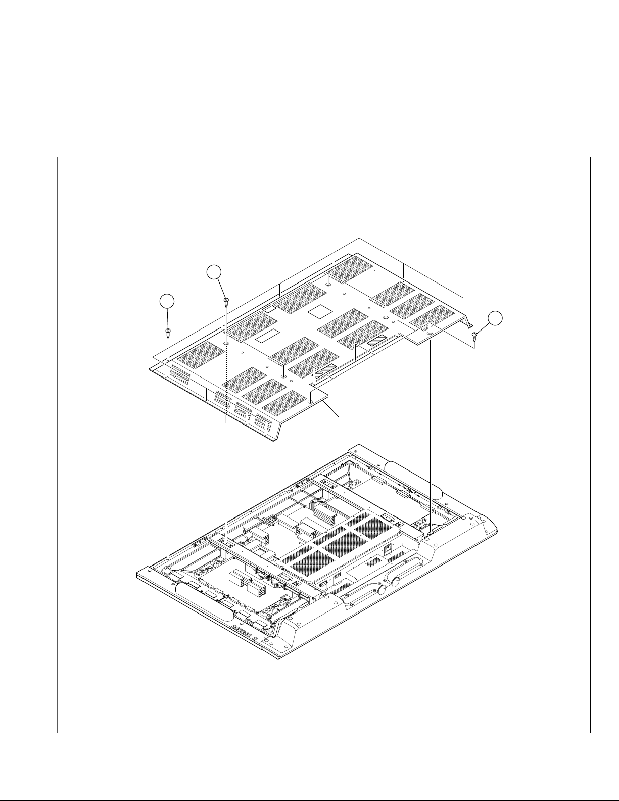
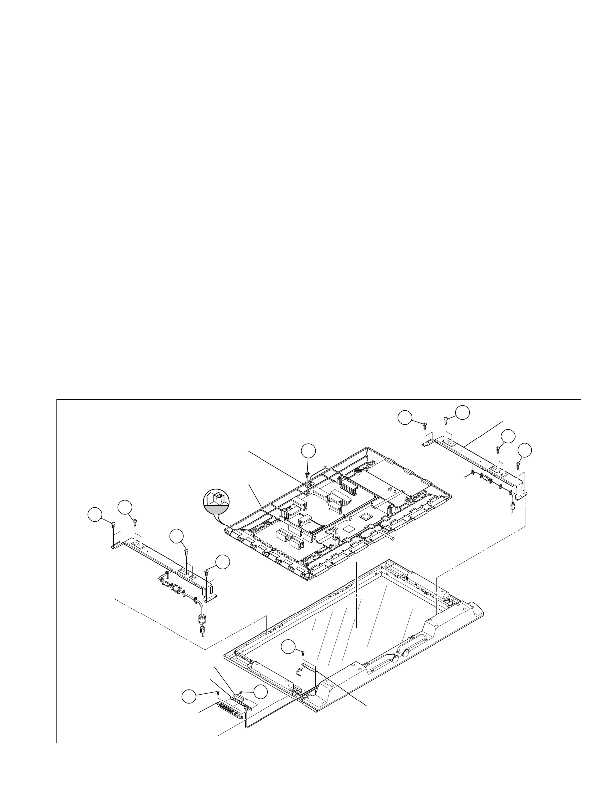
3.1.1 REMOVING THE REAR COVER (Fig. 1)
(1) Remove the power cord and system cable.
(2) Remove the 12 screws[A] and 9 screws [B], and remove
the REAR COVER.
(x5)
B
REAR COVER
Fig.1
(No.YA018) 1-9
Page 10
3.1.2 REMOVING THE TERMINAL COVER (Fig.2)
• Remove the REAR COVER.
(1) Remove the 6 screws [C], withdraw the CHASSIS SHIELD
BRACKET.
(2) Remove the 2 screws [D], the 2 screws [E] and 3 screws
[F], and remove the TERMINAL COVER.
(3) Disconnect the connectors [CN60CB], [CN60SR],
[CN60SL] from the SPEAKER.
(4) Remove the 4 screws [J], and remove the AUDIO PWB.
NOTE:
• It is advisable to take note of the connecting location
(connector number) of the removed connectors.
3.1.3 REMOVING THE LINE FILTER PWB (Fig. 2)
• Remove the REAR COVER.
• Remove the CHASSIS SHIELD BRACKET.
• Remove the TERMINAL COVER.
(1) Remove the LINE FILTER INSULATOR.
CAUTION:
• On that occasion,please pay attention to the claws on both
sides.
(2) Disconnect the connector [CN8001] from the SMPS PWB.
(3) Remove the 2 screws [G], 1 screw [H] and 1 screw [I], and
remove the LINE FILTER PWB.
NOTE:
• It is advisable to take note of the connecting location
(connector number) of the removed connectors.
3.1.4 REMOVING THE AUDIO PWB (Fig.2)
• Remove the REAR COVER.
• Remove the CHASSIS SHIELD BRACKET.
• Remove the TERMINAL COVER.
(1) Disconnect the connector [CN9003] from the VIDEO SMPS
PWB.
(2) Disconnect the connectors [CN00A],[CN00C],[CN00D]
from the DISPLAY INTERFACE PWB.
LINE FILTER
INSULATOR
J
(x4)
DISPLAY
INTERFACE
PWB
CHASSIS SHIELD
BRACKET
(x3)
(x6)
AUDIO
PWB
K
C
O
(x2)
3.1.5 REMOVING THE DISPLAY INTERFACE PWB (Fig.2 )
• Remove the REAR COVER.
• Remove the CHASSIS SHIELD BRACKET.
• Remove the TERMINAL COVER.
(1) Disconnect the connectors [CN00A], [CN00C], [CN00D],
[CN00E], [CN00Q], [CN00T], [CN00V], [CN00X], [CNLVDS]
from the DISPLAY INTERFACE PWB.
(2) Remove the 3 screws [K], the 1 screw [L], the 2 screws [M]
and the 2 screws [N], and withdraw the DISPLAY
INTERFACE PWB.
NOTE:
• It is advisable to take note of the connecting location
(connector number) of the removed connectors.
3.1.6 REMOVING THE CHASSIS BASE (Fig.2)
• Remove the REAR COVER.
• Remove the CHASSIS SHIELD BRACKET.
• Remove the TERMINAL COVER.
• Remove the LINE FILTER PWB.
• Remove the AUDIO PWB.
• Remove the DISPLAY INTERFACE PWB.
(1) Remove the 2 screws [O], and remove the CHASSIS BASE.
G
H
a
I
LINE FILTER
PWB
O
F
F
D
D
TERMINAL
COVER
1-10 (No.YA018)
L
CHASSIS BASE
(x2)
M
Fig.2
E
(x2)
N
(x2)
a
F
Page 11
3.1.7 REMOVING THE TEMP. SENSOR PWB (Fig.3)
• Remove the REAR COVER.
(1) Disconnect the connector [CN00V] from the DISPLAY
INTERFACE PWB.
(2) Remove the 1 screw [P], and withdraw the TEMP. SENSOR
PWB.
NOTE:
• It is advisable to take note of the connecting location
(connector number) of the removed connectors.
3.1.8 REMOVING THE DISPLAY SWITCH PWB (Fig.3 )
• Remove the BACK COVER(R).
(1) Remove the 2 screws [Q], and withdraw the DISPLAY UNIT
SET.
(2) Remove the 3 screws [R], and remove the CONTROL
KNOB and INSULATOR.
(3) Disconnect the connector [CN00T] from the DISPLAY
SWITCH PWB.
NOTE:
• It is advisable to take note of the connecting location
(connector number) of the removed connectors.
3.1.9 REMOVING THE DISPLAY LED PWB (Fig.3 )
• Remove the BACK COVER(R).
(1) Remove the 2 screws [Q], and withdraw the CONTROL
KNOB.
(2) Remove the 2 screws [S], and withdraw the DISPLAY LED
PWB.
(3) Disconnect the connector [CN100X] from the DISPLAY LED
PWB.
NOTE:
• It is advisable to take note of the connecting location
(connector number) of the removed connectors.
3.1.10 REMOVING THE PDP UNIT (Fig.3)
• Remove the REAR COVER.
• Remove the CHASSIS SHIELD BRACKET.
• Remove the TERMINAL COVER.
• Remove the CHASSIS BASE(with each PWB affixed on the
CHASSIS BASE).
(1) Disconnect the connector [CN8001] from the SMPS PWB.
(2) Disconnect the connector [CN9003] from the VIDEO SMPS
PWB.
(3) Disconnect the connectors [CN00A], [CN00E], [CN00Q],
[CN00T], [CN00V], [CN00X], [CNLVDS] from the DISPLAY
INTERFACE PWB.
(4) Remove the 8 screws [T] and the 8 screws [U], and remove
the BACK BRACKET(R) and the BACK BRACKET(L).
(5) Lift the PDP upright and remove it with enough care not to
impose shock to the PDP.
NOTE:
• It is advisable to take note of the connecting location
(connector number) of the removed connectors.
CAUTION:
• Two or more people are required to remove the PDP unit.
• The gas pouring port is covered with the protection
material.In operation, be careful not to damage the gas
pouring port.
• Do not touch the front side (glass) of the PDP with your
fingers.
(x2)
U
(x2)
T
(x2)
TEMP. SENSOR PWB
PDP UNIT
(x2)
Q
GAS insertion
hole
T
(x2)
(x2)
R
(x3)
U
T
(x2)
U
INSULATOR
DISPLAY SWITCH PWB
(x2)
P
S
BACK BRACKET
U
(x2)
T
(x2)
CONTROL KNOB
DISPLAY LED PWB
Fig.3
(No.YA018) 1-11
Page 12

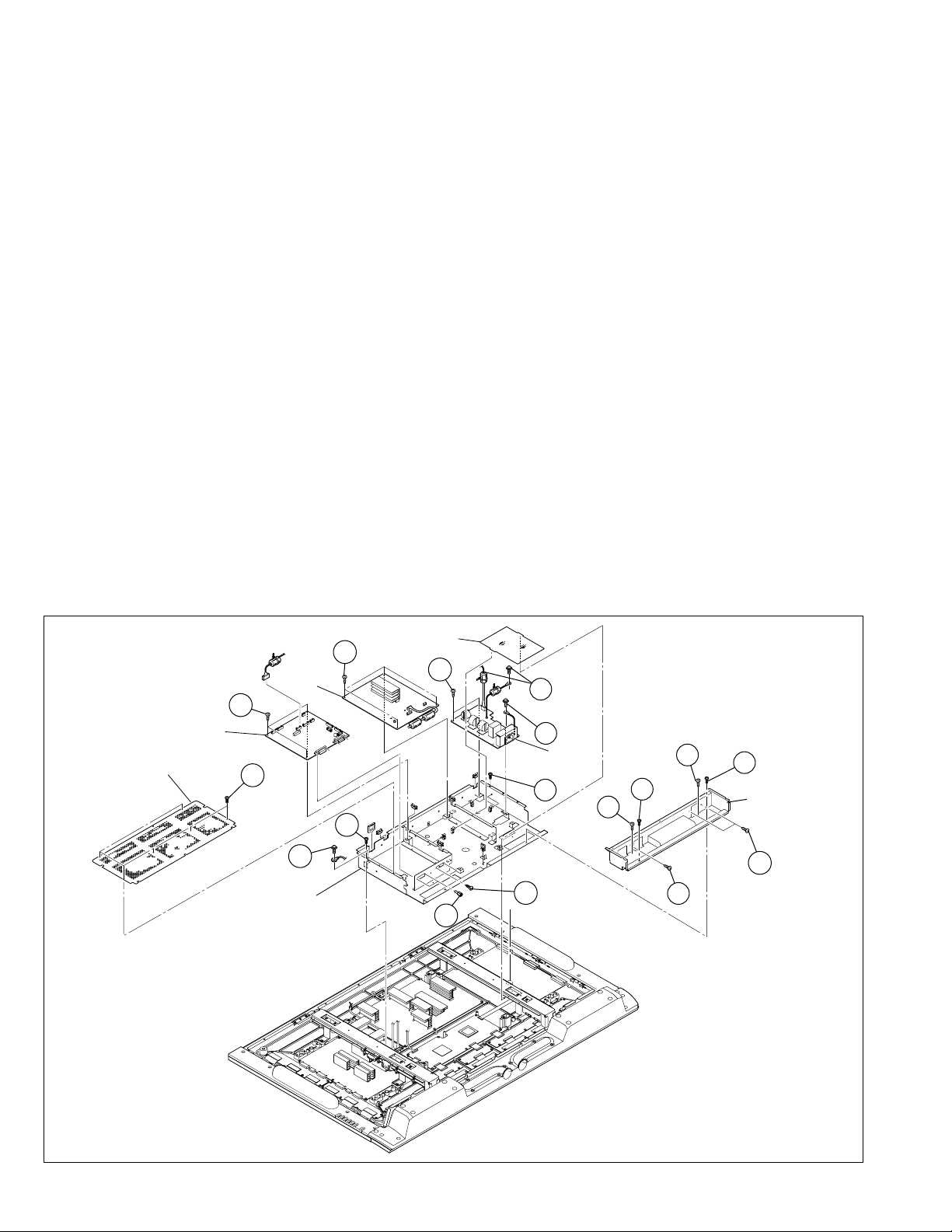
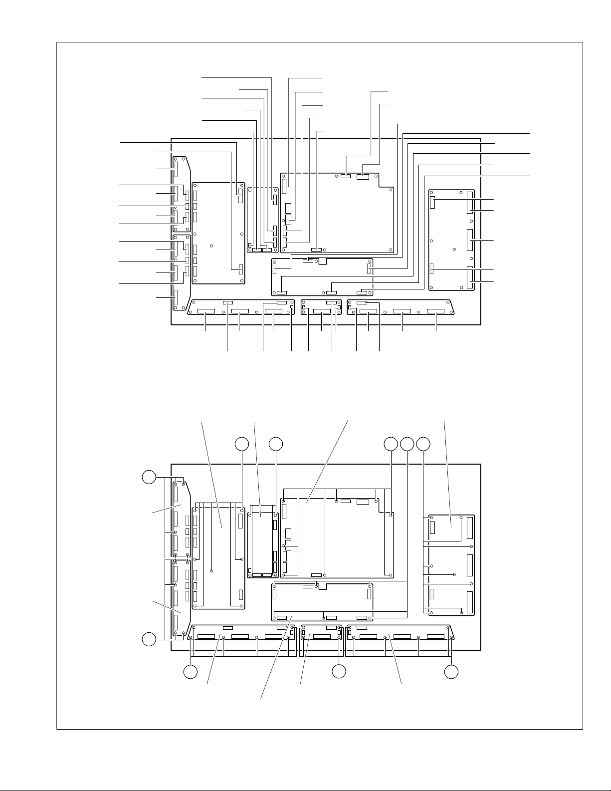
3.1.11 REMOVING THE PWB IN PDP UNIT
3.1.11.1 REMOVING THE SMPS PWB (Fig.4 )
• Remove the PDP UNIT.
(1) Disconnect the connectors [CN8002], [CN8003],
[CN8004], [CN8006], [CN8007], [CN8008], [CN8009] from
the SMPS PWB.
(2) Remove the 8 screws [V], and remove the SMPS PWB.
NOTE:
• It is advisable to take note of the connecting location
(connector number) of the removed connectors.
3.1.11.2 REMOVING THE X-MAIN PWB (Fig.4 )
• Remove the PDP UNIT.
(1) Disconnect the connectors [CN4001], [CN4002],
[CN4003], [CN4004], [CN4005] from the X-MAIN PWB.
(2) Remove the 8 screws [W], and remove the X-MAIN PWB.
NOTE:
• It is advisable to take note of the connecting location
(connector number) of the removed connectors.
3.1.11.3 REMOVING THE Y-MAIN PWB (Fig.4 )
• Remove the PDP UNIT.
(1) Disconnect the connectors [CN5001], [CN5002],
[CN5003], [CN5004], [CN5005],[CN5006], [CN5007],
[CN5008] from the Y-MAIN PWB.
(2) Remove the 7 screws [X], and remove the Y-MAIN PWB.
NOTE:
• It is advisable to take note of the connecting location
(connector number) of the removed connectors.
3.1.11.4 REMOVING THE LOGIC-MAIN PWB (Fig.4 )
• Remove the PDP UNIT.
(1) Disconnect the connector [CN8008] from the SMPS PWB.
(2) Disconnect the connector [CN4002] from the X-MAIN PWB.
(3) Disconnect the connector [CN5001] from the Y-MAIN PWB.
(4) Disconnect the connector [CN401] from the E-BUFFER
PWB.
(5) Disconnect the connector [CN402] from the F-BUFFER
PWB.
(6) Disconnect the connector [CN403] from the G-BUFFER
PWB.
(7) Remove the 6 screws [Y], and remove the LOGIC-MAIN
PWB.
NOTE:
• It is advisable to take note of the connecting location
(connector number) of the removed connectors.
3.1.11.5 REMOVING THE Y-BUFFER-U PWB (Fig. 4)
• Remove the PDP UNIT.
(1) Disconnect the connectors [CN5401], [CN5402],
[CN5403], [CN5404], [CN5405],[CN5406] from the YBUFFER-U PWB.
(2) Remove the 5 screws [Z], and remove the Y-BUFFER-U
PWB.
NOTE:
• It is advisable to take note of the connecting location
(connector number) of the removed connectors.
3.1.11.6 REMOVING THE Y-BUFFER-L PWB (Fig.4 )
• Remove the PDP UNIT.
(1) Disconnect the connectors [CN5501], [CN5502],
[CN5503], [CN5504], [CN5505],[CN5506] from the YBUFFER-L PWB.
(2) Remove the 5 screws [a], and remove the Y-BUFFER-L
PWB.
NOTE:
• It is advisable to take note of the connecting location
(connector number) of the removed connectors.
3.1.11.7 REMOVING THE E-BUFFER PWB (Fig.4 )
• Remove the PDP UNIT.
(1) Disconnect the connectors [CN401], [CN806], [EC1], [EC2],
[EC3],[EF1] from the E-BUFFER PWB.
(2) Remove the 6 screws [b], and remove the E-BUFFER
PWB.
NOTE:
• It is advisable to take note of the connecting location
(connector number) of the removed connectors.
3.1.11.8 REMOVING THE F-BUFFER PWB (Fig.4 )
• Remove the PDP UNIT.
(1) Disconnect the connectors [CN402], [FC4], [FE1], [FG1],
from the F-BUFFER PWB.
(2) Remove the 4 screws [c], and remove the F-BUFFER PWB.
NOTE:
• It is advisable to take note of the connecting location
(connector number) of the removed connectors.
3.1.11.9 REMOVING THE G-BUFFER PWB(Fig.4 )
• Remove the PDP UNIT.
(1) Disconnect the connectors [CN403], [GC5], [GC6], [GC7],
[GF1] from the G-BUFFER PWB.
(2) Remove the 6 screws [d], and remove the G-BUFFER
PWB.
NOTE:
• It is advisable to take note of the connecting location
(connector number) of the removed connectors.
3.1.11.10 REMOVING THE VIDEO SMPS PWB (Fig.4 )
• Remove the PDP UNIT.
(1) Disconnect the connectors [CN9005], [CN9006], [CN9007]
from the VIDEO SMPS PWB.
(2) Remove the 4 screws [e], and remove the VIDEO SMPS
PWB.
NOTE:
• It is advisable to take note of the connecting location
(connector number) of the removed connectors.
1-12 (No.YA018)
Page 13
CN5008
CN5404
CN5406
CN5405
CN5505
CN5506
CN5504
CN5001
CN5401
CN5402
CN5403
CN5501
CN5502
CN5503
CN9005
CN9006
CN9001
CN9007
CN9002
CN9004
CN8003
BUFFER
CN8004
CN8007
CN8008
CN8009
CN8002
CN201
CN803
CN101
CN401
CN402
CN403
CN4001
CN4003
CN4004
CN4002
CN4005
Y-MAIN PWB
Z
(x5)
Y-BUFFER-U
PWB
Y-BUFFER-L
PWB
EC1
EC2 EC3
CN806 CN401 CN402 CN403
EF1
VIDEO SMPS PWB
(x7)
X
e
(x4)
FC4 FC4
FE1
GF1
SMPS PWB
GC5 GC6 GC7
X-MAIN PWB
(x6)(x8) (x8)
V
Y W
(x5)
a
(x6)
b
E-BUFFER PWB G-BUFFER PWBF-BUFFER PWB
LOGIC-MAIN PWB
Fig.4
(x4) (x6)
c
d
(No.YA018) 1-13
Page 14
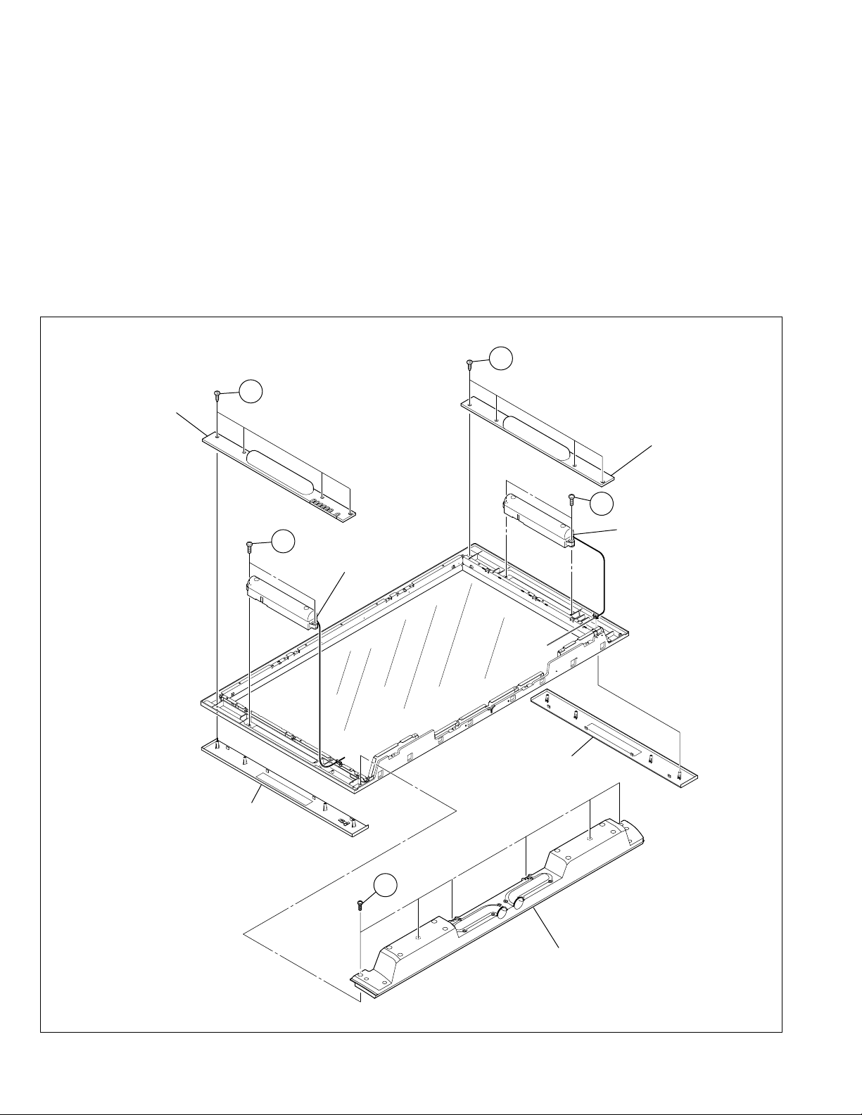
3.1.12 REMOVING THE DD SPEAKER ASS’Y(R) AND DD SPAKER
ASS’Y(L) (Fig. 5)
• Remove the REAR COVER
(1) Remove the 4 screws [f], withdraw the BACK COVER(R)
and the SP HOLDER ASS’Y.
(2) Disconnect the connector [CN60SR] from the AUDIO PWB.
(3) Remove the 2 screws [g], and remove the DD SPAKER
ASS’Y(R).
(4) Remove the 4 screws [h], and withdraw the BACK
COVER(L) and the SP HOLDER.
(5) Disconnect the connector [CN60SL] from the AUDIO PWB.
(6) Remove the 2 screws [i], and remove the DD SPEAKER
ASS’Y(L).
NOTE:
• It is advisable to take note of the connecting location
(connector number) of the removed connectors.
f
BACK COVER(R)
(x4)
3.1.13 REMOVING THE WOOFER SPEAKER ASS’Y (Fig. 5)
• Remove the REAR COVER.
(1) Disconnect the connector [CN60CB] from the AUDIO PWB.
(2) Remove the 6 screws [j], and remove the WOOFER
SPEAKER ASS’Y.
NOTE:
• It is advisable to take note of the connecting location
(connector number) of the removed connectors.
h
(x4)
BACK COVER(L)
SP HOLDER ASS'Y
g
(x2)
DD SPEAKER ASS'Y(R)
(x6)
j
SP HOLDER
i
(x2)
DD SPEAKER ASS'Y(L)
1-14 (No.YA018)
WOOFER SPEAKER ASS'Y
Fig. 5
Page 15
3.1.14 REMOVING THE FRONT FILTER (Fig. 6)
• Remove the REAR COVER.
• Remove the CHASSIS SHIELD BRACKET.
• Remove the TERMINAL COVER.
• Remove the CHASSIS BASE (with each PWB affixed on the
CHASSIS BASE).
• Remove the PDP UNIT.
(1) Remove the 4 mounting bosses [k], the 6 screws [l] and
the 6 screws [m], and withdraw the GLASS HOLDERS.
(2) Remove the FRONT FILTER with enough care not to
damage it.
m
(x6)
o
(x2)
TOP FRAME BRACKET
GLASS HOLDER
o
BOTTOM FRAME BRACKET
(x2)
n
3.1.15 REMOVING THE TOP FRAME BRACKET, BOTTOM FRAME
BRACKET AND SIDE FRAME BRACKET (Fig. 6)
• Remove the REAR COVER.
• Remove the CHASSIS SHIELD BRACKET.
• Remove the TERMINAL COVER.
• Remove the CHASSIS BASE (with each PWB affixed on the
CHASSIS BASE).
• Remove the PDP UNIT.
(1) Remove the 4 screws [n], the 6 screws [o] and the 1 screws
[p], and remove the TOP FRAME BRACKET, BOTTOM
FRAME BRACKET and SIDE FRAME BRACKET.
k
(x4)
n
(x2)
o
c
SIDE FRAME BRACKET
o
(x2)
l
(x6)
SIDE FRAME BRACKET
p
FRONT FILTER
c
FRONT PANEL
Fig. 6
(No.YA018) 1-15
Page 16

3.2 DISASSEMBLY OF PROCEDURE [RECEIVER UNIT]
3.2.1 REMOVING THE TOP COVER
(1) Remove the 4 screws [A] on the both left and right sides.
(2) Remove the 3 screws [B] on the rear side.
(3) Lift upwards and withdraw the TOP COVER.
3.2.2 REMOVING THE FRONT PANEL
• Remove the TOP COVER.
(1) Remove the 1 screw [C] and 1 screw [D].
(2) Disengage the 2 claws [E] on the both left and right sides.
(3) Disengage the 2 claws [F] on the bottom side.
(4) Withdraw the FRONT PANEL in a front direction.
3.2.3 REMOVING THE DAMPER (INSIDE FRONT PANEL)
• Remove the TOP COVER.
• Remove the FRONT PANEL.
(1) Remove the 1 screw [G], and remove the DAMPER.
3.2.4 REMOVING THE FORNT CONTROL PWB
• Remove the TOP COVER.
• Remove the FRONT PANEL.
(1) Remove the 4 screws [H], and remove the FRONT
CONTROL PWB.
3.2.5 REMOVING THE REAR COVER
• Remove the TOP COVER.
(1) Remove the 2 screws [I], 2 screws [J], 2 screws [K], 14
screws [L], 3 screws [M] and 1 connector [N].
(2) Withdraw the REAR COVER in a rear direction.
3.2.9 REMOVING THE MAIN PWB AND RECEIVER POWER PWB
• Remove the TOP COVER.
• Remove the REAR COVER.
• Remove the DIST PWB and DIST RELAY PWB.
• Remove the MI-COM PWB and MI-COM INTERFACE PWB.
• Remove the AV JACK PWB and AV SWITCH PWB.
(1) Remove the 2 screws [S] and 2 screws [T]. Then, lift
upwards and withdraw the MAIN PWB.
(2) Remove the 6 screws [U] and remove the MI-COM
HOLDER and the RECEIVER POWER PWB.
3.2.10 REMOVING THE AC INLET
• Remove the TOP COVER.
• Remove the REAR COVER.
• Remove the DIST PWB and DIST RELAY PWB.
(1) Remove the 1 screw [V] and remove the AC INLET.
3.2.6 REMOVING THE DIST PWB AND DIST RELAY PWB
• Remove the TOP COVER.
• Remove the REAR COVER.
(1) Remove the 2 screws [O] and 2 screws [P].
(2) Lift upwards and withdraw the SUPPORT BRACKET, the
DIST PWB and the DIST RELAY PWB.
(3) Remove the 6 screws [Q] and remove the SUPPORT
BRACKET.
(4) Pull right and left and remove the DIST PWB and DIST
RELAY PWB.
3.2.7
REMOVING THE MI-COM PWB AND MI-COM INTERFACE PWB
• Remove the TOP COVER.
• Remove the REAR COVER.
• Remove the DIST PWB and DIST RELAY PWB.
(1) Remove the 1 screw [R] and remove the PB HOLDER.
(2) Lift upwards and withdraw the MI-COM PWB and the MI-
COM INTERFACE PWB.
(3) Pull right and left and remove the MI-COM PWB and the
MI-COM INTERFACE PWB.
3.2.8 REMOVING THE AV JACK PWB AND AV SWITCH PWB
• Remove the TOP COVER.
• Remove the REAR COVER.
• Remove the DIST PWB and DIST RELAY PWB.
• Remove the MI-COM PWB and MI-COM INTERFACE PWB.
(1) Lift upwards and withdraw the AV JACK PWB and the AV
SWITCH PWB.
(2) Pull right and left and remove the AV JACK PWB and the AV
SWITCH PWB.
1-16 (No.YA018)
Page 17

TOP COVER
a
A
(x2)
B
(x3)
A
(x2)
FRONT PANEL
FRONT PANEL
(BACK SIDE)
C
DAMPER
PB HOLDER
d
D
F
G
b
MI-COM
INTERFACE
PWB
FRONT
CONTROL
PWB
FRONT PANEL
Q
SUPPORT
BRACKET
O
MI-COM PWB
f
c
DIST PWB
P
O
DIST RELAY
PWB
MI-COM
HOLDER
U
P
e
f
U
U
(x4)
Q
(x5)
AV JACK PWB
AV SWITCH PWB
S
S
RECEIVER POWER PWB
e
H
F
(x4)
T
T
MAIN PWB
V
E
AC INLET
I
(x2)
J
E
REAR COVER
d
(x2)
K
(x2)
R
a
c
BOTTOM CASE
b
N
M
M
L
L
(x10)
M
(x4)
FRONT DOOR
Fig. 7
(No.YA018) 1-17
Page 18

3.3 REPLACEMENT OF MEMORY IC
SERVICE MENU SCREEN
SYSTEM CONSTANT SET SCREEN
3.3.1 MEMORY IC
This unit uses the nonvolatile memory IC.
The memory IC memories data for video and deflection circuits. To replace the memory IC without the data written, malfunctions
might occurred while power is on, and the normal image might not appear. When replacing the memory IC, be sure to use the IC
written with the initial values of data.
3.3.2 PROCEDURE FOR REPLACING THE MEMORY IC
1. Power off
Switch the power off and unplug the power cord from the
wall outlet.
2. Replacing the memory IC
Replace the memory IC with new one. Be sure to use the
memory IC written with the initial data values.
3. Power on
Plug the power cord into the wall outlet and switch the
power on.
4. Check and setting of SYSTEM CONSTANT SET
(1) Press the [INFORMATION] key and the [MUTING] key
on the remote control unit simultaneously.
The SERVICE MENU screen will be displayed.(See
Fig.1.)
(2) In the SERVICE MENU, press the [INFORMATION] key
and [MUTING] key simultaneously. Then, the SYSTEM
CONSTANT SET screen will be displayed.(See Fig.2.)
(3) Check whether the setting values of the SYSTEM
CONSTANT SET are the same as those indicated in
Table1.
(4) Press the [INFORMATION] key twice to return to the
normal screen.
5. Receive channel setting
Refer to the OPERATING INSTRUCTIONS and set the
receive channels (channels preset).
6. User setting
Check the user setting values in Table 2 and Table 3. If
setting value is different, set the correct value.
For setting, refer to the OPERATING INSTRUCTIONS.
7. Setting of SERVICE MENU
Verify the setting for each setting item in the SERVICE
MENU.(See Table 4.) If readjustment is necessary,
perform adjustment referring to “ADJUSTMENTS
PROCEDURE”.
SERVICE MENU SCREEN
SERVICE MENU
1. IF 2. V/C
3. AUDIO 4. DD/CM
5. VSM PRESET 6. STATUS
7. VNR 8. IP
9. SHIPPING (OFF) 0. BUS FREE
1-9 : SELECT i : EXIT
Fig.1
SYSTEM CONSTANT SET SCREEN
SYSTEM CONSTANT SET
1. DESTINATION ASIA
-/+ : STORE i : EXIT
OK
Fig.2
3.3.3 FACTORY SETTING VALUE
3.3.3.1 SETTING OF SYSTEM CONSTANT SET
Setting item Setting content Setting value
DESTINATION ASIA / EURO ASIA
3.3.3.2 SETTING OF SWITCHS ON DISPLAY UNIT AND REMOTE CONTROL UNIT
Setting item Setting value
POWER OFF
SHIPPING CHANNEL PR1
PRESET CHANNEL Refer to OPERATION INSTRUCTIONS
VOLUME 10
ZOOM PANORAMIC
CINEMA SURROUND OFF
Table 2
1-18 (No.YA018)
Table 1
Page 19

3.3.3.3 SETTING OF MENU SCREEN
Setting item Setting value
PICTURE SETTING
PICTURE MODE BRIGHT
CONTRAST +13
BRIGHT -1
SHARP +6
COLOUR +2
WHITE BALANCE MID
PICTURE FEATURES
DIGITAL VNR AUTO
Super Digi Pure AUTO
COLOUR SYSTEM TV: Depeend on PR/CH
VIDEO: AUTO
PULL DOWN AUTO
4:3 AUTO ASPECT PANORAMIC
COLOUR MANAGEMENT ON
PIP Right below
SOUND SETTING
STEREO / I•II Stereo sound
BASS Center
TREBLE Center
BALANCE Center
SPEAKER ON
BBE ON
CINEMA SURROUND OFF
A.H.B. ON
Setting item Setting value
HEADPHONE
VOLUME 20
TV SPEAKER OFF
OUTPUT MAIN
VIDEO SETTING
ID LIST Space
FEATURES
SLEEP TIMER OFF
BLUE BACK ON
CHANNEL GUARD ID NO. 0000
ALL CH : OFF
REFRESH OFF
PICTURE SHIFT FAST
INSTALL
LANGUAGE ENGLISH
AUTO PROGRAM GROUP-1
EDIT / MANUAL Only for PR/CH
Table 3
3.3.3.4 VSM PRESET SETTING
Item No. Item
1 CONT -16~16 +13 0 -7 --- --- --2 BRIGHT -16~16 -1 0 0 --- --- --3 SHARP -16~16 +6 0 -2 --- --- --4 COLOUR -16~16 +2 0 -2 --- --- --5 TINT -16~16 0 0 0 --- --- ---
1 WDR R -128~127 --- --- --- -22 0 0
2 WDR G -128~127 --- --- --- -21 0 -12
3 WDR B -128~127 --- --- --- 0 0 -5
3.3.3.4.1 Setting of VSM PRESET
(1) Enter "5.VSM PRESET" from the SERVICE MENU.
(2) Press the [OK] key to select BRIGHT/STD/SOFT/COOL/NORMAL/WARM mode.
(3) Select the setting item using the [FUNCTION (
(4) Set the value using the [FUNCTION (#/$)] key.
(5) Press the [OK] key to save the value.
(6) Press the [INFORMATION] key twice to return to the normal screen.
Variable
range
PICTURE MODE WHITE BALANCE
BRIHGT STANDARD SOFT COOL MID WARM
!/")] key.
Setting value
(No.YA018) 1-19
Page 20

3.3.3.5 SERVICE MENU SETTING ITEMS
Service menu Setting item
1. IF 1. VCO
2. ATT ON/OFF [Do not adjust]
2. VC 1.CUT OF R
2.CUT OF G
3.CUT OF B
4.DRIVE R
5.DRIVE G
6.DRIVE B
7.TWN HI R
8.TWN HI B
9.BRIGHT
10.CONT
11.TWN BRG
12.TWN CNT
13.COLOUR
14.HUE
15.BY GAIN
16.TWN COL
17.TWN TNT
18.B OF MR
19.B OF MB
20.B OF SR
21.B OF SB
22.M BOF ST
23.M ROF ST
S01 ~ S99
A01 ~ A17
PDA01 ~ PDA12
PDB01 ~ PDB22
RGA01 ~ RGA03
Service menu Setting item
5.VSM PRESET PICTURE MODE
1.CONT
2.BRIGHT
3.SHARP
4.COLOUR
5.TINT
WHITE BALANCE.
1.WDR R
2.WDR G
3.WDR B
6.STATUS [Do not adjust]
7.VNR
[Do not adjust] 1.MYLV
2.ONMVF
3.MYCOR
4.MYGA
5.YEGON
6.YEGL
7.YLTL
8.MCLV
9.MCGA
10.MCCOR
11.CLTL
12.YNGA
13.COR_OF
14.LPF_OF
15.YCTL
16.YNCL
17.YNCON
3.AUDIO 1.ERROR LIMIT
[Do not adjust] 2.A2 ID THR
3.Q-PEAK
4.SOUND LEVEL
4.DD/CM DDT01 ~ DDT34
CMT01 ~ CMT57
DDP01 ~ DDP37
CMP01 ~ CMP03
OSD-G
OSD-B
OSD-R
1-20 (No.YA018)
8.IP PPA001 ~ PPA008
[Do not adjust] PPB001 ~ PPB036
PPC001 ~ PPC007
PPD001 ~ PPD016
ADS001 ~ ADS034
IPA001 ~ IPA120
IPB001 ~ IPB088
IPC001 ~ IPC044
IPD001 ~ IPD058
9.SHIPPING(OFF)
Table 4
[Do not select under the adjustment]
Page 21

3.4 REPLACEMENT OF CHIP COMPONENT
A
B
C
3.4.1 CAUTIONS
(1) Avoid heating for more than 3 seconds.
(2) Do not rub the electrodes and the resist parts of the pattern.
(3) When removing a chip part, melt the solder adequately.
(4) Do not reuse a chip part after removing it.
3.4.2 SOLDERING IRON
(1) Use a high insulation soldering iron with a thin pointed end of it.
(2) A 30w soldering iron is recommended for easily removing parts.
3.4.3 REPLACEMENT STEPS
1. How to remove Chip parts
[Resistors, capacitors, etc.]
(1) As shown in the figure, push the part with tweezers and
alternately melt the solder at each end.
(2) Shift with tweezers and remove the chip part.
2. How to install Chip parts
[Resistors, capacitors, etc.]
(1) Apply solder to the pattern as indicated in the figure.
(2) Grasp the chip part with tweezers and place it on the
solder. Then heat and melt the solder at both ends of
the chip part.
[Transistors, diodes, variable resistors, etc.]
(1) Apply extra solder to each lead.
SOLDER
SOLDER
(2) As shown in the figure, push the part with tweezers and
alternately melt the solder at each lead. Shift and remove
the chip part.
Note :
After removing the part, remove remaining solder from
the pattern.
[Transistors, diodes, variable resistors, etc.]
(1) Apply solder to the pattern as indicated in the figure.
(2) Grasp the chip part with tweezers and place it on the
solder.
(3) First solder lead A as indicated in the figure.
(4) Then solder leads B and C.
A
B
C
(No.YA018) 1-21
Page 22

SECTION 4
ADJUSTMENT
4.1 ADJUSTMENT PREPARATION
NOTE:
Prior to the following procedure, be sure to connect the
receiver unit and the display unit.
(1) You can make the necessary adjustments for this unit
with either the remote control unit or with the adjustment
equipment and parts as given below.
(2) Adjustment with the remote control unit is made on the
basis of the initial setting values, however, the new
setting values which set the screen to its optimum
condition may differ from the initial settings.
(3) Make sure that AC power is turned on correctly.
(4) Turn on the power for the set and test equipment before
use, and start the adjustment procedures after waiting at
least 30 minutes.
(5) Unless otherwise specified, prepare the most suitable
reception or input signal for adjustment.
(6) Never touch any adjustment parts, which are not specified
in the list for this variable resistors, transformers, trimmer
capacitors, etc.
(7) Presetting before adjustment.
Unless otherwise specified in the adjustment instructions,
preset the following functions with the remote control unit.
4.3 MAIN PARTS LOCATIONS
4.3.1 RECEIVER UNIT
!
Presetting position
Setting item Settings
PICTURE MODE STANDARD
PICTURE adjustments All center (00)
WHITE BALANCE NORMAL
DIGITAL VNR MIN
Super Digi Pure AUTO
SOUND adjustments All center (00)
ZOOM FULL
4.2 MEASURING INSTRUMENT AND FIXTURES
• DC voltmeter (or Digital voltmeter)
• Oscilloscope
• Signal generator (Pattern generator) [PAL/SECAM/NTSC]
• Remote control unit
1-22 (No.YA018)
DIST RELAY PWB
MI-COM PWB
MI-COM
INTERFACE
PWB
FRONT CONTROL PWB
Fig.1
DIST PWB
AV JACK PWB
AV SW PWB
RECEIVER POWER PWB
MAIN PWB
Page 23

4.3.2 DISPLAY UNIT
TOP
TEMP. SENSOR PWB
CN4001 CN4003
CN8002CN8009
CN8003NCCN8005
CN8006
CN9005
CN8004
CN9008
CN4004
CN8003 CN8001
CN8007
CN9003CN9001
CN9002
CN9006
CN4005
CN101
CN803
LA03
CN201
CN4002
NC
CN2002
CN403
CN402
CN401
GC5 GC6 GC7
CN403
GF1
FC4
CN402
FC4
EF1 FE1
CN401
LINE FILTER PWB
A
EQ
PW
C2
XV
NC
T
LVD S
NC
F
CHASSIS BASE
F9901
POWER
B
A
C
DD
SR CB SL
C
C1
NC
CONNECTOR
AUDIO PWB
MAIN SPEAKER(L)MAIN SPEAKER(R)
WOOFER SPEAKER
PDP UNIT
CN5401
CN5008
CN5002
CN5404 CN5404 CN5405 CN5505 CN5506 CN5504
CN5402 CN5403 CN5501 CN5502 CN5503
CN5006
CN5003
CN5004
CN5001
CN5007
CN5005
CN806
EC1 EC2 EC3
DISPLAY
INTERFACE
PWB
DISPLAY SWITCH
PWB
DISPLAY LED
PWB
(No.YA018) 1-23
Page 24

4. 4 SERVICE MENU SCREEN
SERVICE MENU
SERVICE MENU
1. IF 2. V/C
3. AUDIO 4. DD/CM
5. VSM PRESET 6. STATUS
7. VNR 8. IP
9. SHIPPING (OFF) 0. BUS FREE
1-9 : SELECT i : EXIT
DDT01 ~ DDT34
CMT01 ~ CMT57
DDP01 ~ DDP37
CMP01 ~ CMP03
OSD-G
OSD-B
OSD-R
PICTURE MODE
BRIGHT
STD
SOFT
WHITE BALANCE
COOL
MID
WARM
1. SOFT
2. TELE TEXT
3. ASPECT
4. IC
5. DEBUG
6. PANEL
4. DD/CM
DD/CM PAL
DDT01 0000
- / +
- / +
1. CONT
2. BRIGHT
3. SHARP
4. COLOUR
5.
1.
2.
3.
- / +
: STORE i : EXIT
OK
5. VSM PRESET
VSM PRESET BRIGHT
1.CONT
OK
: STORE i : EXIT
TINT
WDR R
WDR G
WDR B
6. STATUS
STATUS
1.SOFT
OK
: SELECT i : EXIT
000
1.IF
IF SERVICE MENU
1. VCO
2. ATT ON/OFF
1-2 : SELECT i : EXIT
2. VC
V/C
1. CUT OF R
OK
- / +
: STORE i : EXIT
1. ERROR LIMIT 0100
ERROR LIMIT =
C_AD_BITS =
OK
- / +
PAL
0000
3. AUDIO
AUDIO
: STORE i : EXIT
0000
00000000
1. CUT OF R
2. CUT OF G
3. CUT OF B
4. DRIVE R
5. DRIVE G
6. DRIVE B
7. TWN HI R
8. TWN HI B
9. BRIGHT
10. CONT
11. TWN BRG
12. TWN CNT
13. COLOUR
14. HUE
1. ERR LIMIT
2. A2 ID THR
3. Q
PEAK
4. SOUND LEVEL
15. BY GAIN
16. TWN COL
17. TWN TNT
18. B OF MR
19. B OF MB
20. B OF SR
21. B OF SB
22. M BOF ST
23. M ROF ST
S01 ~ S99
A01 ~ A17
PDA01 ~ PDA12
PDB01 ~ PDB22
RGA01 ~ RGA03
1. MYLV
2. ONMVF
3. MYCOR
4. MYGA
5. YEGON
6. YEGL
7. YLTL
8. MCLV
9. MCGA
10. MCCOR
11. CLTL
12. YNGA
13. COR_OF
14. LPF_OF
15. YCTL
16. YNCL
17. YNCON
PPA001 ~ PPA008
PPB001 ~ PPB036
PPC001 ~ PPC007
PPD001 ~ PPD016
ADS001 ~ ADS034
IPA001 ~ IPA120
IPB001 ~IPB088
IPC001 ~ IPC044
IPD001 ~ IPD058
1-24 (No.YA018)
7. VNR
VNR
1.MYLV
OK
- / +
- / +
: STORE i : EXIT
8. IP
IP FULL PAL
0000 PPA001 0000
: STORE i : EXIT
OK
000
Fig.3
Page 25

4.5 BASIC OPERATION OF THE SERVICE MENU
SERVICE MENU SCREEN
4.5.1 TOOL OF SERVICE MENU OPERATION
Operate the SERVICE MENU with the remote control unit.
4.5.2 HOW TO ENTER THE SERVICE MENU MODE
(1) Press the [INFORMATION] key and the [MUTING] key of
the REMOTE CONTROL UNIT simultaneously, and the
SERVICE MENU screen of Fig.4 will be displayed.
(2) When the Main Menu is displayed, press any key of the [1]
to [0] key to enter the corresponding menu mode.
*Press any of the [1] to [0] keys before the Service Menu
mode disappears.
(3) Select the service item using the [FUNCTION (
!/")] key.
(4) Set the value using the [FUNCTION (#/$)] key.
(5) Press the [OK] key to save the value.
4.5.5 SETTINGS OF THE SERVICE MENUS
4.5.5.1 [1. IF (VCO adjustment, ATT setting)]
[Do not change settings of items that are not included in the
"ADJUSTMENT PROCEDURE".]
4.5.5.2 [2. VC (VIDEO setting)]
[Do not change settings of items that are not included in the
"ADJUSTMENT PROCEDURE".]
Sets output data to the video circuit.
• [Function (!/")] key
For scrolling up/down the setting items.
• [Function (#/$)] key
For scrolling up/down the setting values.
SERVICE MENU SCREEN
SERVICE MENU
1. IF 2. V/C
3. AUDIO 4. DD/CM
5. VSM PRESET 6. STATUS
7. VNR 8. IP
9. SHIPPING (OFF) 0. BUS FREE
1-9 : SELECT i : EXIT
Fig.4
3.5.2 HOW TO EXIT THE SERVICE MENU MODE
Press the [INFORMATION] key to exit the Service Menu mode.
3.5.3 SERVICE CONTROL KEY LAYOUT ON THE REMOTE
CONTROL UNIT
MUTING
1~0
INFOMATION
ZOOM
OK
FUNCTION /
FUNCTION /
4.5.5.3 [3. AUDIO (SOUND setting)]
[Do not adjust]
4.5.5.4 [4. DD/CM (Panel picture processing setting)]
[Do not change settings of items that are not included in the
"ADJUSTMENT PROCEDURE".]
Sets output data to the deflection circuit.
• [Function (!/")] key
For scrolling up/down the setting items.
→→
→ DDT01...
→→
↔↔
↔ CMT01...
↔↔
↔↔
↔ DDPM01...
↔↔
↔↔
↔ CMP01...
↔↔
↔↔
↔ OSD-G
↔↔
←←
←
←←
• [Zoom (red)] key
For switching to the next item.
→→
→
DDT01
→→
→→
→
CMT01
→→
→→
→
DDP01
→→
→→
→
CMP01
→→
→→
→
OSD-G –
→→
• [Function (#/$)] key
For scrolling up/down the setting values.
4.5.5.5 [5. VSM PRESET (PICTURE preset setting)]
[Refer to page 1-19.]
4.5.5.6 [6. STATUS]
(The version of software, the aspect, and the state of
debugging are displayed. )
[Setting for this item is not required in servicing]
4.5.5.7 [7. VNR (Noise reduction setting)]
[Do not adjust]
Sets output data to the digital noise reduction circuit.
4.5.5.8 [8. IP (DIST setting)]
[Do not adjust]
Sets output data to the DIST circuit.
Fig.5
4.5.5.9 [9. SHIPPING (OFF)]
[Setting for this item is not required in servicing]
4.5.5.10 [10. BUE FREE]
[Setting for this item is not required in servicing]
(No.YA018) 1-25
Page 26

4. 6 DEFAULT VALUES IN THE SERVICE MENU SETTING MODE
• Perform fine-tuning based on the "default values" using the remote control when in the SERVICE MENU setting mode.
• The "default values" serve only as an indication rough standard and therefore the values with which optimal display can be
achieved may be different from the default values. But, don't change the values that are not written in "ADJUSTMENT
PROCEDURE". They are fixed values.
4.6.1 [2. VC]
4.6.1.1 VIDEO SYSTEM
Setting value
Item No. Item
1 CUT OF R 0000~0255 0088 ←←←←0000 ←←←
2 CUT OF G 0000~0255 0101 ←←←←0000 ←←←
3 CUT OF B 0000~0255 0106 ←←←←0000 ←←←
4 DRIVE R 0000~0255 0129 ←←←←0000 ←←←
5 DRIVE G 0000~0255 0112 ←←←←0000 ←←←
6 DRIVE B 0000~0255 0110 ←←←←0000 ←←←
7 TWN HI R 0000~0127 0065 ←←←←0000 ←←←
8 TWN HI B 0000~0127 0063 ←←←←0000 ←←←
9 BRIGHT 0000~0255 0013 ← ← ←←←←←←
10 CONT 0000~0015 0011 ←←←←0000 ←←←
11 TWN BRG 0000~0127 0081 ←←←←0000 ←←←
12 TWN CNT 0000~0015 0011 ←←←←0000 ←←←
13 COLOUR 0000~0015 0007 ← 0000 ← 0009 0000 ←←←
14 HUE 0000~0063 0007 ← 0034 ← 0034 0000 ←←0063
15 BY GAIN 0000~0063 0043 ← 0000 ← 0043 0000 ←←0043
16 TWN COL 0000~0015 0009 ← 0002 ← 0009 0002 0009 0002 ←
17 TWN TNT 0000~0063 0034 ← ← ←←←←←←
18 B OF MR 0000~0015 0008 ← ← ←←←←←←
19 B OF MB 0000~0015 0008 ← ← ←←←←←←
20 B OF SR 0000~0015 0008 ← ← ←←←←←←
21 B OF SB 0000~0015 0008 ← ← ←←←←←←
22 M BOFSET 0000~0007 0000 ← ← ←←←←←←
23 M ROFSET 0000~0007 0000 ← ← ←←←←←←
Variable range
TV EXT-1 / 2 / 3 / 5 EXT-4
PAL SECAM PAL SECAM NTSC 625i 525i 625p 525p
Item No. Item
S01 COLOUR 0000~0255 0120 0135 0124
S02 HUE -128~0127 0000 0000 -014
S03 (NO DISPLAY) -128~0127 0000 0000 0000
S04 (NO DISPLAY) -128~0127 0000 0000 0000
S05 BRIGHT 0000~0255 0039 0039 0032
S06 CONT 0000~0255 0088 0088 0088
S07 (NO DISPLAY) -128~0127 0000 0000 0000
S08 (NO DISPLAY) -128~0127 0000 0000 0000
S09 (NO DISPLAY) 0000~0255 0140 0140 0140
S10 (NO DISPLAY) -128~0127 0000 0000 0000
S11 (NO DISPLAY) -128~0127 0006 0006 0006
S12 (NO DISPLAY) 0000~0003 0000 0000 0000
S13 R GAIN 0000~0255 0255 0255 0255
S14 (NO DISPLAY) -128~0127 0000 0000 0000
S15 G GAIN 0000~0255 0241 0241 0241
S16 (NO DISPLAY) -128~0127 0000 0000 0000
S17 B GAIN 0000~0255 0019 0019 0019
S18 (NO DISPLAY) -128~0127 0000 0000 0000
S19 (NO DISPLAY) 0000~0255 0128 0128 0128
1-26 (No.YA018)
Variable range
PAL SECAM NTSC
Setting value
Page 27

Item No. Item
S20 (NO DISPLAY) -128~0127 0000 0000 0000
S21 (NO DISPLAY) 0000~0255 0128 0128 0128
S22 (NO DISPLAY) -128~0127 0000 0000 0000
S23 (NO DISPLAY) 0000~0255 0128 0128 0128
S24 (NO DISPLAY) -128~0127 0000 0000 0000
S25 (NO DISPLAY) 0000/0001 0000 0000 0000
S26 (NO DISPLAY) 0000/0001 0000 0000 0000
S27 (NO DISPLAY) 0000/0001 0000 0000 0000
S28 (NO DISPLAY) 0000/0001 0001 0001 0001
S29 (NO DISPLAY) 0000/0001 0000 0000 0000
S30 (NO DISPLAY) 0000~0031 0001 0001 0001
S31 (NO DISPLAY) 0000~0063 0010 0010 0003
S32 (NO DISPLAY) 0000~0063 0040 0040 0030
S33 (NO DISPLAY) 0000/0001 0001 0001 0001
S34 (NO DISPLAY) 0000/0001 0001 0001 0001
S35 (NO DISPLAY) 0000/0001 0000 0000 0000
S36 (NO DISPLAY) 0000~0031 0000 0000 0000
S37 (NO DISPLAY) 0000~0255 0225 0225 0200
S38 (NO DISPLAY) 0000~0063 0045 0045 0050
S39 (NO DISPLAY) 0000~0063 0060 0060 0060
S40 (NO DISPLAY) 0000/0001 0001 0001 0001
S41 (NO DISPLAY) 0000/0001 0000 0000 0000
S42 (NO DISPLAY) 0000~0003 0001 0001 0001
S43 (NO DISPLAY) 0000~0031 0024 0024 0024
S44 (NO DISPLAY) 0000~0003 0001 0001 0001
S45 (NO DISPLAY) 0000~0003 0001 0001 0001
S46 (NO DISPLAY) 0000~0015 0015 0015 0015
S47 (NO DISPLAY) 0000~0015 0015 0015 0015
S48 (NO DISPLAY) 0000~0015 0015 0015 0015
S49 (NO DISPLAY) 0000/0001 0000 0000 0000
S50 (NO DISPLAY) 0000~0255 0009 0009 0009
S51 (NO DISPLAY) 0000/0001 0000 0000 0000
S52 (NO DISPLAY) 0000~0255 0061 0061 0061
S53 (NO DISPLAY) 0000/0001 0000 0000 0000
S54 (NO DISPLAY) 0000~0255 0004 0004 0004
S55 (NO DISPLAY) 0000/0001 0000 0000 0000
S56 (NO DISPLAY) 0000~0255 0057 0057 0057
S57 (NO DISPLAY) 0000~0255 0000 0000 0000
S58 (NO DISPLAY) 0000~0015 0000 0000 0000
S59 (NO DISPLAY) 0000~0255 0013 0013 0013
S60 (NO DISPLAY) 0000~0015 0000 0000 0000
S61 (NO DISPLAY) 0000/0001 0001 0001 0001
S62 (NO DISPLAY) 0000~0127 0012 0012 0012
S63 (NO DISPLAY) 0000/0001 0000 0000 0000
S64 (NO DISPLAY) 0000~0127 0000 0000 0000
S65 (NO DISPLAY) 0000~0003 0003 0003 0003
S66 (NO DISPLAY) 0000~0003 0001 0001 0001
S67 (NO DISPLAY) 0000~0003 0002 0002 0002
S68 (NO DISPLAY) 0000~0015 0000 0000 0002
S69 (NO DISPLAY) 0000~0063 0019 0019 0019
S70 (NO DISPLAY) 0000/0001 0001 0001 0001
S71 (NO DISPLAY) 0000~0255 0255 0255 0255
S72 (NO DISPLAY) 0000~0255 0255 0255 0255
S73 (NO DISPLAY) 0000~0255 0255 0255 0255
Variable range
PAL SECAM NTSC
Setting value
(No.YA018) 1-27
Page 28

Item No. Item
S74 (NO DISPLAY) 0000~0031 0000 0000 0000
S75 (NO DISPLAY) 0000~0031 0000 0000 0000
S76 (NO DISPLAY) -127~0128 0000 0000 0000
S77 (NO DISPLAY) -127~0128 0000 0000 0000
S78 (NO DISPLAY) 0000~0255 0255 0255 0255
S79 (NO DISPLAY) 0000~0255 0000 0000 0000
S80 (NO DISPLAY) 0000~0255 0255 0255 0255
S81 (NO DISPLAY) 0000~0255 0000 0000 0000
S82 (NO DISPLAY) 0000~0255 0255 0255 0255
S83 (NO DISPLAY) 0000~0255 0000 0000 0000
S84 (NO DISPLAY) 0000~0015 0000 0000 0000
S85 (NO DISPLAY) 0000~0255 0011 0011 0011
S86 (NO DISPLAY) 0000~0255 0130 0130 0130
S87 (NO DISPLAY) 0000~0003 0000 0000 0000
S88 (NO DISPLAY) 0000~0007 0007 0007 0007
S89 (NO DISPLAY) 0000~0255 0030 0030 0030
S90 (NO DISPLAY) 0000~0127 0000 0000 0000
S91 (NO DISPLAY) 0000~0007 0007 0007 0007
S92 (NO DISPLAY) 0000~0031 0031 0031 0031
S93 (NO DISPLAY) 0000~0007 0007 0007 0007
S94 (NO DISPLAY) 0000~0031 0031 0031 0031
S95 (NO DISPLAY) 0000~0255 0060 0060 0075
S96 (NO DISPLAY) 0000~0015 0006 0006 0006
S97 (NO DISPLAY) 0000~0003 0035 0035 0040
S98 (NO DISPLAY) 0000~0063 0003 0003 0000
S99 (NO DISPLAY) 0000~0063 0000 0000 0000
Variable range
PAL SECAM NTSC
Setting value
4.6.1.2 AUDIO SYSTEM
Item No. Item
A01 (NO DISPLAY) 0000~0007 0001
A02 (NO DISPLAY) 0000~0007 0002
A03 (NO DISPLAY) 0000~0007 0003
A04 (NO DISPLAY) 0000~0007 0003
A05 (NO DISPLAY) 0000~0009 0002
A06 (NO DISPLAY) 0000~0015 0005
A07 (NO DISPLAY) 0000~0015 0006
A08 (NO DISPLAY) 0000~0015 0003
A09 (NO DISPLAY) 0000~0007 0000
A10 (NO DISPLAY) 0000~0007 0000
A11 (NO DISPLAY) 0000~0063 0017
A12 (NO DISPLAY) 0000~0063 0010
A13 (NO DISPLAY) 0000~0003 0000
A14 (NO DISPLAY) 0000~0007 0000
A15 (NO DISPLAY) 0000~0003 0000
A16 (NO DISPLAY) 0000~0003 0000
A17 (NO DISPLAY) 0000~0003 0000
Item No. Item
PDA01 (NO DISPLAY) 0000~0255 0000
PDA02 (NO DISPLAY) 0000~0255 0094
PDA03 (NO DISPLAY) 0000~0255 0128
PDA04 (NO DISPLAY) 0000~0255 0003
PDA05 (NO DISPLAY) 0000/0001 0001
PDA06 (NO DISPLAY) 0000/0001 0000
Variable range
Variable range
Setting value
Setting value
1-28 (No.YA018)
Page 29

Item No. Item
PDA07 (NO DISPLAY) 0000~0255 0150
PDA08 (NO DISPLAY) 0000~0255 0150
PDA09 (NO DISPLAY) 0000~0255 0002
PDA10 (NO DISPLAY) 0000~0255 0059
PDA11 (NO DISPLAY) 0000~0255 0000
PDA12 (NO DISPLAY) 0000~0127 0000
Variable range
Setting value
Item No. Item
PDB01 (NO DISPLAY) 0000~0063 0000
PDB02 (NO DISPLAY) 0000~0255 0000
PDB03 (NO DISPLAY) 0000~0255 0000
PDB04 (NO DISPLAY) 0000~0255 0000
PDB05 (NO DISPLAY) 0000~0255 0000
PDB06 (NO DISPLAY) 0000~0001 0001
PDB07 (NO DISPLAY) 0000~0001 0001
PDB08 (NO DISPLAY) 0000~0255 0138
PDB09 (NO DISPLAY) 0000~0255 0138
PDB10 (NO DISPLAY) 0000~0255 0138
PDB11 (NO DISPLAY) 0000~0001 0001
PDB12 (NO DISPLAY) 0000~0001 0000
PDB13 (NO DISPLAY) 0000~0031 0031
PDB14 (NO DISPLAY) 0000~0001 0000
PDB15 (NO DISPLAY) 0000~0001 0001
PDB16 (NO DISPLAY) 0000~0255 0250
PDB17 (NO DISPLAY) 0000~0001 0000
PDB18 (NO DISPLAY) 0000~0255 0200
PDB19 (NO DISPLAY) 0000~0127 0004
PDB20 (NO DISPLAY) 0000~0127 0004
PDB21 (NO DISPLAY) 0000~0001 0000
PDB22 (NO DISPLAY) 0000~0001 0000
Variable range
Setting value
Item No. Item
RGA01 (NO DISPLAY) 0000~0001 0001
RGA02 (NO DISPLAY) 0000~0001 0001
RGA03 (NO DISPLAY) 0000~0001 0001
4.6.2 [3.AUDIO] (MULTISOUND SYSTEM) (*All fixed)
Item No. Item
1 ERROR LIMIT 0000~0FF0 0100
2 A2 ID THR 0000~00FF 0019
3 Q-PEAK - 4 SOUND LEVEL F00F~FFFF FFFF
Variable range
Variable range
Setting value
Setting value
(No.YA018) 1-29
Page 30

4.6.3 [4.DD/CM]
NOTE:
• For reference, initial setting values (except OSD-G/B/R) in the following conditions are written here.
Input signal :PAL/SECAM/NTSC
Picture mode :Standard
Zoom :Full
Multi screen :Single screen
Colour temp. :Normal
Item No. Item
DDT01 (NO DISPLAY) 0000~0015 0000 0000 0000
DDT02 (NO DISPLAY) 0000~0255 0022 0022 0022
DDT03 (NO DISPLAY) 0000~0255 0240 0240 0240
DDT04 (NO DISPLAY) 0000~0255 0255 0255 0255
DDT05 (NO DISPLAY) 0000~0255 0255 0255 0255
DDT06 (NO DISPLAY) 0000~0255 0255 0255 0255
DDT07 (NO DISPLAY) 0000~0003 0000 0000 0000
DDT08 (NO DISPLAY) 0000~0255 0255 0255 0255
DDT09 (NO DISPLAY) 0000~0003 0000 0000 0000
DDT10 (NO DISPLAY) 0000~0255 0000 0000 0000
DDT11 (NO DISPLAY) 0000~0007 0000 0000 0000
DDT12 (NO DISPLAY) 0000~0255 0090 0090 0090
DDT13 (NO DISPLAY) 0000~0255 0000 0000 0000
DDT14 (NO DISPLAY) 0000~0003 0000 0000 0000
DDT15 (NO DISPLAY) 0000~0007 0007 0007 0000
DDT16 (NO DISPLAY) 0000~0255 0151 0151 0151
DDT17 (NO DISPLAY) 0000/0001 0001 0001 0001
DDT18 (NO DISPLAY) 0000/0001 0001 0001 0001
DDT19 (NO DISPLAY) 0000~0063 0001 0001 0001
DDT20 (NO DISPLAY) 0000~0015 0000 0000 0000
DDT21 (NO DISPLAY) 0000~0015 0000 0000 0000
DDT22 (NO DISPLAY) 0000~0015 0000 0000 0000
DDT23 (NO DISPLAY) 0000~0015 0000 0000 0000
DDT24 (NO DISPLAY) 0000/0001 0000 0000 0000
DDT25 (NO DISPLAY) 0000/0001 0000 0000 0000
DDT26 (NO DISPLAY) 0000/0001 0000 0000 0000
DDT27 (NO DISPLAY) 0000~0007 0001 0001 0001
DDT28 (NO DISPLAY) 0000~0255 0023 0023 0023
DDT29 (NO DISPLAY) 0000~0003 0002 0002 0002
DDT30 (NO DISPLAY) 0000/0001 0000 0000 0000
DDT31 (NO DISPLAY) 0000~0007 0002 0002 0002
DDT32 (NO DISPLAY) 0000~0255 0100 0100 0100
DDT33 (NO DISPLAY) 0000~0255 0000 0000 0000
DDT34 (NO DISPLAY) 0000~0255 0032 0032 0032
Variable range
PAL SECAM NTSC
Setting value
Item No. Item
CMT01 (NO DISPLAY) 0000~0003 0000 0000 0000
CMT02 (NO DISPLAY) 0000~0255 0105 0105 0093
CMT03 (NO DISPLAY) 0000~0255 0020 0020 0010
CMT04 (NO DISPLAY) 0000~0255 0020 0020 0020
CMT05 (NO DISPLAY) 0000~0063 0005 0005 0060
CMT06 (NO DISPLAY) -128~0127 0005 0005 0001
CMT07 (NO DISPLAY) -128~0127 0000 0000 0000
CMT08 (NO DISPLAY) -128~0127 -004 -004 -004
CMT09 (NO DISPLAY) -128~0127 0000 0000 0000
1-30 (No.YA018)
Variable range
PAL SECAM NTSC
Setting value
Page 31

Item No. Item
CMT10 (NO DISPLAY) 0000~0003 0000 0000 0000
CMT11 (NO DISPLAY) 0000~0255 0155 0155 0164
CMT12 (NO DISPLAY) 0000~0255 0020 0020 0020
CMT13 (NO DISPLAY) 0000~0255 0020 0020 0020
CMT14 (NO DISPLAY) 0000~0063 0057 0057 0062
CMT15 (NO DISPLAY) -128~0127 0005 0005 0008
CMT16 (NO DISPLAY) -128~0127 0000 0000 0000
CMT17 (NO DISPLAY) -128~0127 0000 0000 0000
CMT18 (NO DISPLAY) -128~0127 0000 0000 0000
CMT19 (NO DISPLAY) 0000~0003 0000 0000 0000
CMT20 (NO DISPLAY) 0000~0255 0191 0191 0200
CMT21 (NO DISPLAY) 0000~0255 0040 0040 0030
CMT22 (NO DISPLAY) 0000~0255 0030 0030 0030
CMT23 (NO DISPLAY) 0000~0063 0057 0057 0059
CMT24 (NO DISPLAY) -128~0127 0010 0010 0005
CMT25 (NO DISPLAY) -128~0127 0020 0020 0015
CMT26 (NO DISPLAY) -128~0127 0010 0010 0010
CMT27 (NO DISPLAY) -128~0127 0015 0015 0015
CMT28 (NO DISPLAY) 0000~0003 0001 0001 0001
CMT29 (NO DISPLAY) 0000~0255 0078 0078 0071
CMT30 (NO DISPLAY) 0000~0255 0030 0030 0035
CMT31 (NO DISPLAY) 0000~0255 0030 0030 0040
CMT32 (NO DISPLAY) 0000~0063 0005 0005 0057
CMT33 (NO DISPLAY) -128~0127 0005 0005 -002
CMT34 (NO DISPLAY) -128~0127 0010 0010 0010
CMT35 (NO DISPLAY) -128~0127 0000 0000 -005
CMT36 (NO DISPLAY) -128~0127 0015 0015 0020
CMT37 (NO DISPLAY) 0000~0255 0064 0064 0064
CMT38 (NO DISPLAY) 0000~0255 0068 0068 0064
CMT39 (NO DISPLAY) 0000~0255 0074 0074 0080
CMT40 (NO DISPLAY) -128~0127 0000 0000 0000
CMT41 (NO DISPLAY) -128~0127 0010 0010 0000
CMT42 (NO DISPLAY) 0000/0001 0000 0000 0000
CMT43 (NO DISPLAY) 0000~0255 0128 0128 0128
CMT44 (NO DISPLAY) 0000/0001 0001 0001 0001
CMT45 (NO DISPLAY) 0000~0255 0080 0080 0080
CMT46 (NO DISPLAY) 0000/0001 0000 0000 0000
CMT47 (NO DISPLAY) 0000~0255 0070 0070 0070
CMT48 (NO DISPLAY) 0000/0001 0001 0001 0001
CMT49 (NO DISPLAY) 0000/0001 0001 0001 0001
CMT50 (NO DISPLAY) 0000~0031 0021 0021 0021
CMT51 (NO DISPLAY) 0000~0031 0021 0021 0021
CMT52 (NO DISPLAY) 0000/0001 0000 0000 0000
CMT53 (NO DISPLAY) 0000/0001 0000 0000 0000
CMT54 (NO DISPLAY) 0000~0003 0000 0000 0000
CMT55 (NO DISPLAY) 0000/0001 0000 0000 0000
CMT56 (NO DISPLAY) 0000/0001 0001 0001 0001
CMT57 (NO DISPLAY) 0000/0001 0001 0001 0001
Variable range
PAL SECAM NTSC
Setting value
(No.YA018) 1-31
Page 32

Item No. Item
DDP01 (NO DISPLAY) 0000~0003 0000 0000 0000
DDP02 (NO DISPLAY) 0000~0255 0032 0032 0032
DDP03 (NO DISPLAY) 0000~0003 0002 0002 0002
DDP04 (NO DISPLAY) 0000~0255 0001 0001 0001
DDP05 (NO DISPLAY) 0000~0255 0001 0001 0001
DDP06 (NO DISPLAY) 0000~0003 0001 0001 0001
DDP07 (NO DISPLAY) 0000~0031 0000 0000 0000
DDP08 (NO DISPLAY) 0000~0007 0000 0000 0000
DDP09 (NO DISPLAY) 0000~0255 0176 0176 0176
DDP10 (NO DISPLAY) 0000~0007 0001 0001 0001
DDP11 (NO DISPLAY) 0000~0255 0000 0000 0000
DDP12 (NO DISPLAY) 0000~0007 0007 0007 0007
DDP13 (NO DISPLAY) 0000~0007 0005 0005 0005
DDP14 (NO DISPLAY) 0000~0003 0002 0002 0002
DDP15 (NO DISPLAY) 0000~0015 0001 0001 0001
DDP16 (NO DISPLAY) 0000~0015 0013 0013 0013
DDP17 (NO DISPLAY) 0000~0015 0010 0010 0010
DDP18 (NO DISPLAY) 0000/0001 0000 0000 0000
DDP19 (NO DISPLAY) 0000/0001 0001 0001 0001
DDP20 (NO DISPLAY) 0000~0015 0010 0010 0010
DDP21 (NO DISPLAY) 0000~0015 0006 0006 0006
DDP22 (NO DISPLAY) 0000~0015 0010 0010 0010
DDP23 (NO DISPLAY) 0000~0015 0006 0006 0006
DDP24 (NO DISPLAY) 0000~0015 0010 0010 0010
DDP25 (NO DISPLAY) 0000~0015 0006 0006 0006
DDP26 (NO DISPLAY) 0000~0015 0015 0015 0015
DDP27 (NO DISPLAY) 0000~0015 0004 0004 0004
DDP28 (NO DISPLAY) 0000~0015 0015 0015 0015
DDP29 (NO DISPLAY) 0000~0015 0014 0014 0014
DDP30 (NO DISPLAY) 0000~0015 0010 0010 0010
DDP31 (NO DISPLAY) 0000~0015 0006 0006 0006
DDP32 (NO DISPLAY) 0000~0255 0013 0013 0013
DDP33 (NO DISPLAY) 0000~0255 0133 0133 0133
DDP34 (NO DISPLAY) 0000~0255 0102 0102 0102
DDP35 (NO DISPLAY) 0000~0255 0144 0144 0144
DDP36 (NO DISPLAY) 0000~0255 0013 0013 0013
DDP37 (NO DISPLAY) 0000~0063 0048 0048 0048
Variable range
PAL SECAM NTSC
Setting value
Item No. Item
CMP01 (NO DISPLAY) 0000/0001 0000 0000 0000
CMP02 (NO DISPLAY) 0000/0001 0001 0001 0001
CMP03 (NO DISPLAY) 0000/0001 0001 0001 0001
Item No. Item
OSD-G (NO DISPLAY) 0000~0255 0128 0128 0128
OSD-B (NO DISPLAY) 0000~0255 0123 0123 0123
OSD-R (NO DISPLAY) 0000~0255 0128 0128 0128
1-32 (No.YA018)
Variable range
Variable range
PAL SECAM NTSC
PAL SECAM NTSC
Setting value
Setting value
Page 33

4.6.4 [7.VNR] (*All fixed)
NOTE:
• For reference, initial setting values in the following conditions are written here.
Input signal :PAL/SECAM/NTSC
Picture mode :Standard
Zoom :Full
Multi screen :Single screen
Colour temp. :Normal
Item No. Item
1 MYLV 0000~000F 000E 000E 000E
2 ONMVF 0000/0001 0001 0001 0001
3 MYCOR 0000~001F 0003 0003 0003
4 MYGA 0000~0003 0002 0002 0002
5 YEGON 0000/0001 0001 0001 0001
6 YEGL 0000~000F 0000 0000 0000
7 YL TL 0000~007F 0009 0009 0009
8 MCLV 0000~000F 000E 000E 000E
9 MCGA 0000~0003 0002 0002 0002
10 MCCOR 0000~001F 0003 0003 0003
11 CLTL 0000~007F 0009 0009 0009
1 2 YNGA 0000~0003 0003 0003 0003
13 COR_OF 0000/0001 0000 0000 0000
14 LPF_OF 0000/0001 0000 0000 0000
15 YCTL 0000~000F 0004 0004 0004
16 YNCL 0000~000F 000E 000E 000E
17 YNCON 0000/0001 0001 0001 0001
4.6.5 [8.IP] (*All fixed)
NOTE:
Variable range
PAL SECAM NTSC
Setting value
• For reference, initial setting values in the following conditions are written here.
Input signal :PAL/SECAM/NTSC
Picture mode :Standard
Zoom :Full
Multi screen :Single screen
Colour temp. :Normal
Item No. Item
PPA001 (NO DISPLAY) 0000~00FF 0040 0040 0040
PPA002 (NO DISPLAY) 0000~00FF 0000 0000 0000
PPA003 (NO DISPLAY) 0000~00FF 003D 003D 0048
PPA004 (NO DISPLAY) 0000~00FF 0000 0000 0000
PPA005 (NO DISPLAY) 0000~00FF 0000 0000 0000
PPA006 (NO DISPLAY) 0000~00FF 0001 0001 0001
PPA007 (NO DISPLAY) 0000~00FF 003D 003D 0048
PPA008 (NO DISPLAY) 0000~00FF 0031 0031 0023
Item No. Item
PPB001 (NO DISPLAY) 0000~001F 0000 0000 0000
PPB002 (NO DISPLAY) 0000~00FF 0000 0000 0000
PPB003 (NO DISPLAY) 0000~00FF 0000 0000 0000
PPB004 (NO DISPLAY) 0000~001F 0000 0000 0000
Variable range
Variable range
PAL SECAM NTSC
PAL SECAM NTSC
Setting value
Setting value
(No.YA018) 1-33
Page 34

Item No. Item
PPB005 (NO DISPLAY) 0000~00FF 0000 0000 0000
PPB006 (NO DISPLAY) 0000~00FF 0000 0000 0000
PPB007 (NO DISPLAY) 0000~001F 0000 0000 0000
PPB008 (NO DISPLAY) 0000~00FF 0000 0000 0000
PPB009 (NO DISPLAY) 0000~00FF 0000 0000 0000
PPB010 (NO DISPLAY) 0000~001F 0000 0000 0000
PPB011 (NO DISPLAY) 0000~00FF 0000 0000 0000
PPB012 (NO DISPLAY) 0000~00FF 0000 0000 0000
PPB013 (NO DISPLAY) 0000~001F 0000 0000 0000
PPB014 (NO DISPLAY) 0000~00FF 0000 0000 0000
PPB015 (NO DISPLAY) 0000~00FF 0000 0000 0000
PPB016 (NO DISPLAY) 0000~001F 0000 0000 0000
PPB017 (NO DISPLAY) 0000~00FF 0000 0000 0000
PPB018 (NO DISPLAY) 0000~00FF 0000 0000 0000
PPB019 (NO DISPLAY) 0000~001F 0000 0000 0000
PPB020 (NO DISPLAY) 0000~00FF 0000 0000 0000
PPB021 (NO DISPLAY) 0000~00FF 0000 0000 0000
PPB022 (NO DISPLAY) 0000~001F 0000 0000 0000
PPB023 (NO DISPLAY) 0000~00FF 0000 0000 0000
PPB024 (NO DISPLAY) 0000~00FF 0000 0000 0000
PPB025 (NO DISPLAY) 0000~001F 0000 0000 0000
PPB026 (NO DISPLAY) 0000~00FF 0000 0000 0000
PPB027 (NO DISPLAY) 0000~00FF 0000 0000 0000
PPB028 (NO DISPLAY) 0000~001F 0000 0000 0000
PPB029 (NO DISPLAY) 0000~00FF 0000 0000 0000
PPB030 (NO DISPLAY) 0000~00FF 0000 0000 0000
PPB031 (NO DISPLAY) 0000~001F 0000 0000 0000
PPB032 (NO DISPLAY) 0000~00FF 0000 0000 0000
PPB033 (NO DISPLAY) 0000~00FF 0000 0000 0000
PPB034 (NO DISPLAY) 0000~001F 0000 0000 0000
PPB035 (NO DISPLAY) 0000~00FF 0000 0000 0000
PPB036 (NO DISPLAY) 0000~00FF 0000 0000 0000
Variable range
PAL SECAM NTSC
Setting value
Item No. Item
PPC001 (NO DISPLAY) 0000~000F 0000 0000 0000
PPC002 (NO DISPLAY) 0000~00FF 0012 0012 0012
PPC003 (NO DISPLAY) 0000~00FF 0002 0002 0002
PPC004 (NO DISPLAY) 0000~000F 0000 0000 0000
PPC005 (NO DISPLAY) 0000~00FF 007C 007C 007C
PPC006 (NO DISPLAY) 0000~000F 0000 0000 0000
PPC007 (NO DISPLAY) 0000~00FF 0000 0000 0000
Item No. Item
PPD001 (NO DISPLAY) 0000~00FF 005F 005F 005F
PPD002 (NO DISPLAY) 0000~00FF 0002 0002 0002
PPD003 (NO DISPLAY) 0000~00FF 00F3 00F3 00F3
PPD004 (NO DISPLAY) 0000~00FF 0002 0002 0002
PPD005 (NO DISPLAY) 0000~00FF 0033 0033 0033
PPD006 (NO DISPLAY) 0000~00FF 0000 0000 0000
PPD007 (NO DISPLAY) 0000~00FF 00CA 00CA 00CA
1-34 (No.YA018)
Variable range
Variable range
PAL SECAM NTSC
PAL SECAM NTSC
Setting value
Setting value
Page 35

Item No. Item
PPD008 (NO DISPLAY) 0000~00FF 0000 0000 0000
PPD009 (NO DISPLAY) 0000~00FF 004E 004E 004E
PPD010 (NO DISPLAY) 0000~00FF 0002 0002 0002
PPD011 (NO DISPLAY) 0000~00FF 00E6 00E6 00E6
PPD012 (NO DISPLAY) 0000~00FF 0002 0002 0002
PPD013 (NO DISPLAY) 0000~00FF 0025 0025 0025
PPD014 (NO DISPLAY) 0000~00FF 0000 0000 0000
PPD015 (NO DISPLAY) 0000~00FF 00C9 00C9 00C9
PPD016 (NO DISPLAY) 0000~00FF 0000 0000 0000
Variable range
PAL SECAM NTSC
Setting value
Item No. Item
ADS001 (NO DISPLAY) 0000~00FF 00D7 00D7 00D7
ADS002 (NO DISPLAY) 0000~000F 000F 000F 000F
ADS003 (NO DISPLAY) 0000~0003 0001 0001 0001
ADS004 (NO DISPLAY) 0000~0007 0005 0005 0005
ADS005 (NO DISPLAY) 0000~001F 0016 0016 0016
ADS006 (NO DISPLAY) 0000~00FF 0028 0028 0028
ADS007 (NO DISPLAY) 0000~00FF 0096 0096 0096
ADS008 (NO DISPLAY) 0000~00FF 0020 0020 0020
ADS009 (NO DISPLAY) 0000~00FF 00FF 00FF 00FF
ADS010 (NO DISPLAY) 0000~00FF 00FF 00FF 00FF
ADS011 (NO DISPLAY) 0000~00FF 00FF 00FF 00FF
ADS012 (NO DISPLAY) 0000~007F 0037 0037 0037
ADS013 (NO DISPLAY) 0000~007F 004B 004B 004B
ADS014 (NO DISPLAY) 0000~007F 003D 003D 003D
ADS015 (NO DISPLAY) 0000/0001 0001 0001 0001
ADS016 (NO DISPLAY) 0000/0001 0001 0001 0001
ADS017 (NO DISPLAY) 0000/0001 0000 0000 0000
ADS018 (NO DISPLAY) 0000/0001 0001 0001 0001
ADS019 (NO DISPLAY) 0000/0001 0000 0000 0000
ADS020 (NO DISPLAY) 0000/0001 0000 0000 0000
ADS021 (NO DISPLAY) 0000/0001 0001 0001 0001
ADS022 (NO DISPLAY) 0000/0001 0000 0000 0000
ADS023 (NO DISPLAY) 0000/0001 0000 0000 0000
ADS024 (NO DISPLAY) 0000/0001 0001 0001 0001
ADS025 (NO DISPLAY) 0000/0001 0000 0000 0000
ADS026 (NO DISPLAY) 0000/0001 0001 0001 0001
ADS027 (NO DISPLAY) 0000/0001 0001 0001 0001
ADS028 (NO DISPLAY) 0000/0001 0001 0001 0001
ADS029 (NO DISPLAY) 0000/0001 0000 0000 0000
ADS030 (NO DISPLAY) 0000~001F 0003 0003 0003
ADS031 (NO DISPLAY) 0000/0001 0001 0001 0001
ADS032 (NO DISPLAY) 0000/0001 0000 0000 0000
ADS033 (NO DISPLAY) 0000/0001 0001 0001 0001
ADS034 (NO DISPLAY) 0000~00FF 0032 0032 0032
Variable range
PAL SECAM NTSC
Setting value
Item No. Item
IPA001 (NO DISPLAY) 0000/0001 0001 0001 0001
IPA002 (NO DISPLAY) 0000~003F 000A 000A 0025
IPA003 (NO DISPLAY) 0000~003F 0022 0022 0022
IPA004 (NO DISPLAY) 0000~003F 002A 002A 0025
IPA005 (NO DISPLAY) 0000~0003 0001 0001 0001
Variable range
PAL SECAM NTSC
Setting value
(No.YA018) 1-35
Page 36

Item No. Item
IPA006 (NO DISPLAY) 0000~0003 0001 0001 0001
IPA007 (NO DISPLAY) 0000~000F 000F 000F 000F
IPA008 (NO DISPLAY) 0000~003F 0000 0000 0000
IPA009 (NO DISPLAY) 0000~003F 0008 0008 0008
IPA010 (NO DISPLAY) 0000~003F 001C 001C 0020
IPA011 (NO DISPLAY) 0000~003F 001C 001C 0020
IPA012 (NO DISPLAY) 0000~003F 0020 0020 0020
IPA013 (NO DISPLAY) 0000~0003 0001 0001 0001
IPA014 (NO DISPLAY) 0000~0003 0002 0002 0001
IPA015 (NO DISPLAY) 0000~000F 000F 000F 000F
IPA016 (NO DISPLAY) 0000~003F 000F 000F 000F
IPA017 (NO DISPLAY) 0000/0001 0001 0001 0001
IPA018 (NO DISPLAY) 0000~003F 0003 0003 0012
IPA019 (NO DISPLAY) 0000/0001 0001 0001 0001
IPA020 (NO DISPLAY) 0000/0001 0001 0001 0001
IPA021 (NO DISPLAY) 0000~003F 0030 0030 0030
IPA022 (NO DISPLAY) 0000~0003 0001 0001 0000
IPA023 (NO DISPLAY) 0000~003F 0000 0000 0000
IPA024 (NO DISPLAY) 0000/0001 0001 0001 0001
IPA025 (NO DISPLAY) 0000/0001 0001 0001 0001
IPA026 (NO DISPLAY) 0000~003F 0030 0030 0030
IPA027 (NO DISPLAY) 0000~0003 0001 0001 0000
IPA028 (NO DISPLAY) 0000~003F 0000 0000 0000
IPA029 (NO DISPLAY) 0000~003F 0000 0000 0000
IPA030 (NO DISPLAY) 0000~000F 000F 000F 000F
IPA031 (NO DISPLAY) 0000~0007 0002 0002 0002
IPA032 (NO DISPLAY) 0000~003F 0000 0000 0000
IPA033 (NO DISPLAY) 0000/0001 0001 0001 0001
IPA034 (NO DISPLAY) 0000~003F 0000 0000 0000
IPA035 (NO DISPLAY) 0000/0001 0001 0001 0001
IPA036 (NO DISPLAY) 0000~003F 000D 000D 000D
IPA037 (NO DISPLAY) 0000~003F 000D 000D 000D
IPA038 (NO DISPLAY) 0000~003F 0010 0010 0010
IPA039 (NO DISPLAY) 0000~0003 0001 0001 0001
IPA040 (NO DISPLAY) 0000~0003 0001 0001 0001
IPA041 (NO DISPLAY) 0000~000F 000F 000F 000F
IPA042 (NO DISPLAY) 0000~003F 0005 0005 0005
IPA043 (NO DISPLAY) 0000~003F 0008 0008 0008
IPA044 (NO DISPLAY) 0000~003F 0020 0020 0020
IPA045 (NO DISPLAY) 0000~003F 0020 0020 0020
IPA046 (NO DISPLAY) 0000~003F 0020 0020 0020
IPA047 (NO DISPLAY) 0000~0003 0002 0002 0002
IPA048 (NO DISPLAY) 0000~0003 0002 0002 0002
IPA049 (NO DISPLAY) 0000~000F 0007 0007 0007
IPA050 (NO DISPLAY) 0000~003F 0008 0008 0008
IPA051 (NO DISPLAY) 0000/0001 0001 0001 0001
IPA052 (NO DISPLAY) 0000~003F 0008 0008 0008
IPA053 (NO DISPLAY) 0000/0001 0001 0001 0001
IPA054 (NO DISPLAY) 0000/0001 0001 0001 0001
IPA055 (NO DISPLAY) 0000~003F 0015 0015 0015
IPA056 (NO DISPLAY) 0000~0003 0000 0000 0000
IPA057 (NO DISPLAY) 0000~003F 000A 000A 000A
IPA058 (NO DISPLAY) 0000/0001 0001 0001 0001
IPA059 (NO DISPLAY) 0000/0001 0001 0001 0001
Variable range
PAL SECAM NTSC
Setting value
1-36 (No.YA018)
Page 37

Item No. Item
IPA060 (NO DISPLAY) 0000~003F 0015 0015 0015
IPA061 (NO DISPLAY) 0000~0003 0000 0000 0000
IPA062 (NO DISPLAY) 0000~003F 000A 000A 000A
IPA063 (NO DISPLAY) 0000~003F 003F 003F 003F
IPA064 (NO DISPLAY) 0000~000F 0006 0006 0006
IPA065 (NO DISPLAY) 0000~0007 0001 0001 0001
IPA066 (NO DISPLAY) 0000~003F 0008 0008 0008
IPA067 (NO DISPLAY) 0000/0001 0001 0001 0001
IPA068 (NO DISPLAY) 0000~003F 0027 0027 0027
IPA069 (NO DISPLAY) 0000~0003 0000 0000 0000
IPA070 (NO DISPLAY) 0000~00FF 0000 0000 0000
IPA071 (NO DISPLAY) 0000~000F 0003 0003 0003
IPA072 (NO DISPLAY) 0000~00FF 00F6 00F6 00F6
IPA073 (NO DISPLAY) 0000/0001 0000 0000 0000
IPA074 (NO DISPLAY) 0000/0001 0000 0000 0000
IPA075 (NO DISPLAY) 0000~00FF 0018 0018 0016
IPA076 (NO DISPLAY) 0000/0001 0000 0000 0000
IPA077 (NO DISPLAY) 0000/0001 0000 0000 0000
IPA078 (NO DISPLAY) 0000/0001 0000 0000 0000
IPA079 (NO DISPLAY) 0000/0001 0000 0000 0000
IPA080 (NO DISPLAY) 0000/0001 0000 0000 0000
IPA081 (NO DISPLAY) 0000/0001 0000 0000 0000
IPA082 (NO DISPLAY) 0000/0001 0000 0000 0000
IPA083 (NO DISPLAY) 0000/0001 0000 0000 0000
IPA084 (NO DISPLAY) 0000/0001 0000 0000 0000
IPA085 (NO DISPLAY) 0000/0001 0000 0000 0000
IPA086 (NO DISPLAY) 0000/0001 0000 0000 0000
IPA087 (NO DISPLAY) 0000/0001 0000 0000 0000
IPA088 (NO DISPLAY) 0000/0001 0000 0000 0000
IPA089 (NO DISPLAY) 0000/0001 0000 0000 0000
IPA090 (NO DISPLAY) 0000/0001 0000 0000 0000
IPA091 (NO DISPLAY) 0000~000F 0000 0000 0000
IPA092 (NO DISPLAY) 0000~00FF 0000 0000 0000
IPA093 (NO DISPLAY) 0000~000F 000F 000F 000F
IPA094 (NO DISPLAY) 0000~00FF 00FF 00FF 00FF
IPA095 (NO DISPLAY) 0000~000F 0000 0000 0000
IPA096 (NO DISPLAY) 0000~00FF 0000 0000 0000
IPA097 (NO DISPLAY) 0000~000F 000F 000F 000F
IPA098 (NO DISPLAY) 0000~00FF 00FF 00FF 00FF
IPA099 (NO DISPLAY) 0000~000F 0000 0000 0000
IPA100 (NO DISPLAY) 0000~00FF 0000 0000 0000
IPA101 (NO DISPLAY) 0000~000F 0000 0000 0000
IPA102 (NO DISPLAY) 0000~00FF 0000 0000 0000
IPA103 (NO DISPLAY) 0000~000F 0000 0000 0000
IPA104 (NO DISPLAY) 0000~00FF 0000 0000 0000
IPA105 (NO DISPLAY) 0000~000F 0000 0000 0000
IPA106 (NO DISPLAY) 0000~00FF 0000 0000 0000
IPA107 (NO DISPLAY) 0000~000F 0000 0000 0000
IPA108 (NO DISPLAY) 0000~00FF 0080 0080 0080
IPA109 (NO DISPLAY) 0000~000F 0000 0000 0000
IPA110 (NO DISPLAY) 0000~00FF 0040 0040 0040
IPA111 (NO DISPLAY) 0000~000F 0005 0005 0005
IPA112 (NO DISPLAY) 0000~00FF 0040 0040 0040
IPA113 (NO DISPLAY) 0000~000F 0000 0000 0000
Variable range
PAL SECAM NTSC
Setting value
(No.YA018) 1-37
Page 38

Item No. Item
IPA114 (NO DISPLAY) 0000~00FF 00C0 00C0 00C0
IPA115 (NO DISPLAY) 0000~000F 0002 0002 0002
IPA116 (NO DISPLAY) 0000~00FF 00EF 00EF 00EF
IPA117 (NO DISPLAY) 0000/0001 0000 0000 0000
IPA118 (NO DISPLAY) 0000/0001 0000 0000 0000
IPA119 (NO DISPLAY) 0000/0001 0000 0000 0000
IPA120 (NO DISPLAY) 0000/0001 0000 0000 0000
Variable range
PAL SECAM NTSC
Setting value
Item No. Item
IPB001 (NO DISPLAY) 0000~00FF 0001 0001 0001
IPB002 (NO DISPLAY) 0000~00FF 004C 004C 0047
IPB003 (NO DISPLAY) 0000~000F 0000 0000 0000
IPB004 (NO DISPLAY) 0000~00FF 0000 0000 0000
IPB005 (NO DISPLAY) 0000~000F 0000 0000 0000
IPB006 (NO DISPLAY) 0000~00FF 0086 0086 0099
IPB007 (NO DISPLAY) 0000~000F 0001 0001 0001
IPB008 (NO DISPLAY) 0000~00FF 0040 0040 0040
IPB009 (NO DISPLAY) 0000~000F 0001 0001 0001
IPB010 (NO DISPLAY) 0000~00FF 0009 0009 000E
IPB011 (NO DISPLAY) 0000~000F 0000 0000 0000
IPB012 (NO DISPLAY) 0000~00FF 009F 009F 00A1
IPB013 (NO DISPLAY) 0000~000F 0000 0000 0000
IPB014 (NO DISPLAY) 0000~00FF 0064 0064 006A
IPB015 (NO DISPLAY) 0000~000F 0000 0000 0000
IPB016 (NO DISPLAY) 0000~00FF 0035 0035 0020
IPB017 (NO DISPLAY) 0000~000F 0000 0000 0000
IPB018 (NO DISPLAY) 0000~00FF 002E 002E 0016
IPB019 (NO DISPLAY) 0000~000F 0000 0000 0000
IPB020 (NO DISPLAY) 0000~00FF 0025 0025 0011
IPB021 (NO DISPLAY) 0000~000F 0000 0000 0000
IPB022 (NO DISPLAY) 0000~00FF 0050 0050 0079
IPB023 (NO DISPLAY) 0000~000F 0000 0000 0000
IPB024 (NO DISPLAY) 0000~00FF 0079 0079 0086
IPB025 (NO DISPLAY) 0000~000F 0000 0000 0000
IPB026 (NO DISPLAY) 0000~00FF 0000 0000 0000
IPB027 (NO DISPLAY) 0000~000F 000F 000F 000F
IPB028 (NO DISPLAY) 0000~00FF 0000 0000 0000
IPB029 (NO DISPLAY) 0000~000F 0000 0000 0000
IPB030 (NO DISPLAY) 0000~00FF 0000 0000 0000
IPB031 (NO DISPLAY) 0000~000F 0000 0000 0000
IPB032 (NO DISPLAY) 0000~00FF 0000 0000 0000
IPB033 (NO DISPLAY) 0000~000F 0000 0000 0000
IPB034 (NO DISPLAY) 0000~00FF 0000 0000 0000
IPB035 (NO DISPLAY) 0000~000F 0000 0000 0000
IPB036 (NO DISPLAY) 0000~00FF 0000 0000 0000
IPB037 (NO DISPLAY) 0000/0001 0000 0000 0000
IPB038 (NO DISPLAY) 0000~0007 0000 0000 0000
IPB039 (NO DISPLAY) 0000~000F 0000 0000 0000
IPB040 (NO DISPLAY) 0000~000F 0000 0000 0000
IPB041 (NO DISPLAY) 0000~000F 0000 0000 0000
IPB042 (NO DISPLAY) 0000~00FF 0000 0000 0000
IPB043 (NO DISPLAY) 0000~000F 0000 0000 0000
IPB044 (NO DISPLAY) 0000~00FF 0000 0000 0000
Variable range
PAL SECAM NTSC
Setting value
1-38 (No.YA018)
Page 39

Item No. Item
IPB045 (NO DISPLAY) 0000~000F 0001 0001 0001
IPB046 (NO DISPLAY) 0000~00FF 008B 008B 008B
IPB047 (NO DISPLAY) 0000~000F 0000 0000 0000
IPB048 (NO DISPLAY) 0000~00FF 0000 0000 0000
IPB049 (NO DISPLAY) 0000~000F 0000 0000 0000
IPB050 (NO DISPLAY) 0000~00FF 0002 0002 0002
IPB051 (NO DISPLAY) 0000~000F 0006 0006 0006
IPB052 (NO DISPLAY) 0000~00FF 0000 0000 0000
IPB053 (NO DISPLAY) 0000~000F 0000 0000 0000
IPB054 (NO DISPLAY) 0000~00FF 00D4 00D4 00D4
IPB055 (NO DISPLAY) 0000~000F 0000 0000 0000
IPB056 (NO DISPLAY) 0000~00FF 000A 000A 000E
IPB057 (NO DISPLAY) 0000~000F 0001 0001 0001
IPB058 (NO DISPLAY) 0000~00FF 0016 0016 001A
IPB059 (NO DISPLAY) 0000~0007 0000 0000 0000
IPB060 (NO DISPLAY) 0000~0003 00D6 00D6 00D6
IPB061 (NO DISPLAY) 0000~0003 0000 0000 0000
IPB062 (NO DISPLAY) 0000/0001 0000 0000 0000
IPB063 (NO DISPLAY) 0000~00FF 0000 0000 0000
IPB064 (NO DISPLAY) 0000~00FF 0000 0000 0000
IPB065 (NO DISPLAY) 0000~00FF 0000 0000 0000
IPB066 (NO DISPLAY) 0000/0001 0030 0030 0039
IPB067 (NO DISPLAY) 0000~000F 0006 0006 0006
IPB068 (NO DISPLAY) 0000~000F 0040 0040 0040
IPB069 (NO DISPLAY) 0000~000F 0000 0000 0000
IPB070 (NO DISPLAY) 0000~000F 0000 0000 0000
IPB071 (NO DISPLAY) 0000~00FF 0000 0000 0000
IPB072 (NO DISPLAY) 0000~000F 0000 0000 0000
IPB073 (NO DISPLAY) 0000~00FF 0050 0050 0050
IPB074 (NO DISPLAY) 0000/0001 0080 0080 0080
IPB075 (NO DISPLAY) 0000/0001 0080 0080 0080
IPB076 (NO DISPLAY) 0000/0001 0000 0000 0000
IPB077 (NO DISPLAY) 0000~000F 0000 0000 0000
IPB078 (NO DISPLAY) 0000/0001 0000 0000 0000
IPB079 (NO DISPLAY) 0000~00FF 0000 0000 0000
IPB080 (NO DISPLAY) 0000~000F 000F 000F 000F
IPB081 (NO DISPLAY) 0000~00FF 0000 0000 0000
IPB082 (NO DISPLAY) 0000~000F 0000 0000 0000
IPB083 (NO DISPLAY) 0000~00FF 0000 0000 0000
IPB084 (NO DISPLAY) 0000/0001 0000 0000 0000
IPB085 (NO DISPLAY) 0000/0001 0000 0000 0000
IPB086 (NO DISPLAY) 0000/0001 0000 0000 0000
IPB087 (NO DISPLAY) 0000~000F 0009 0009 000B
IPB088 (NO DISPLAY) 0000/0001 0001 0001 0001
Variable range
PAL SECAM NTSC
Setting value
Item No. Item
IPC001 (NO DISPLAY) 0000~0003 0002 0002 0002
IPC002 (NO DISPLAY) 0000~00FF 0090 0090 0020
IPC003 (NO DISPLAY) 0000/0001 0000 0000 0000
IPC004 (NO DISPLAY) 0000/0001 0000 0000 0000
IPC005 (NO DISPLAY) 0000~000F 0000 0000 0000
IPC006 (NO DISPLAY) 0000~00FF 0000 0000 0000
IPC007 (NO DISPLAY) 0000~000F 0003 0003 0003
Variable range
PAL SECAM NTSC
Setting value
(No.YA018) 1-39
Page 40

Item No. Item
IPC008 (NO DISPLAY) 0000~00FF 00F5 00F5 00F6
IPC009 (NO DISPLAY) 0000~000F 0004 0004 0004
IPC010 (NO DISPLAY) 0000~00FF 005E 005E 005E
IPC011 (NO DISPLAY) 0000~000F 0000 0000 0000
IPC012 (NO DISPLAY) 0000~00FF 0000 0000 0000
IPC013 (NO DISPLAY) 0000~0003 0000 0000 0000
IPC014 (NO DISPLAY) 0000/0001 0000 0000 0000
IPC015 (NO DISPLAY) 0000/0001 0001 0001 0001
IPC016 (NO DISPLAY) 0000~00FF 0016 0016 0000
IPC017 (NO DISPLAY) 0000/0001 0000 0000 0000
IPC018 (NO DISPLAY) 0000~007F 0000 0000 0000
IPC019 (NO DISPLAY) 0000/0001 0000 0000 0000
IPC020 (NO DISPLAY) 0000~007F 0001 0001 0001
IPC021 (NO DISPLAY) 0000~000F 0000 0000 0000
IPC022 (NO DISPLAY) 0000~00FF 008A 008A 0090
IPC023 (NO DISPLAY) 0000~0003 0000 0000 0000
IPC024 (NO DISPLAY) 0000~00FF 001A 001A 0002
IPC025 (NO DISPLAY) 0000/0001 0001 0001 0000
IPC026 (NO DISPLAY) 0000~007F 0001 0001 0004
IPC027 (NO DISPLAY) 0000/0001 0000 0000 0000
IPC028 (NO DISPLAY) 0000~007F 0000 0000 0000
IPC029 (NO DISPLAY) 0000/0001 0001 0001 0001
IPC030 (NO DISPLAY) 0000/0001 0000 0000 0000
IPC031 (NO DISPLAY) 0000/0001 0000 0000 0000
IPC032 (NO DISPLAY) 0000/0001 0000 0000 0000
IPC033 (NO DISPLAY) 0000/0001 0000 0000 0000
IPC034 (NO DISPLAY) 0000/0001 0000 0000 0000
IPC035 (NO DISPLAY) 0000/0001 0000 0000 0000
IPC036 (NO DISPLAY) 0000/0001 0000 0000 0000
IPC037 (NO DISPLAY) 0000/0001 0000 0000 0000
IPC038 (NO DISPLAY) 0000/0001 0000 0000 0000
IPC039 (NO DISPLAY) 0000/0001 0000 0000 0000
IPC040 (NO DISPLAY) 0000/0001 0000 0000 0000
IPC041 (NO DISPLAY) 0000/0001 0000 0000 0000
IPC042 (NO DISPLAY) 0000/0001 0000 0000 0000
IPC043 (NO DISPLAY) 0000/0001 0000 0000 0000
IPC044 (NO DISPLAY) 0000/0001 0000 0000 0000
Variable range
PAL SECAM NTSC
Setting value
Item No. Item
IPD001 (NO DISPLAY) 0000~00FF 0040 0040 0040
IPD002 (NO DISPLAY) 0000~00FF 0000 0000 0000
IPD003 (NO DISPLAY) 0000~00FF 0000 0000 0000
IPD004 (NO DISPLAY) 0000~0007 0000 0000 0000
IPD005 (NO DISPLAY) 0000~00FF 0000 0000 0000
IPD006 (NO DISPLAY) 0000~0007 0006 0006 0006
IPD007 (NO DISPLAY) 0000~00FF 0018 0018 0018
IPD008 (NO DISPLAY) 0000/0001 0000 0000 0000
IPD009 (NO DISPLAY) 0000~000F 0001 0001 0001
IPD010 (NO DISPLAY) 0000~00FF 0062 0062 0062
IPD011 (NO DISPLAY) 0000~000F 0005 0005 0005
IPD012 (NO DISPLAY) 0000~00FF 002B 002B 002B
IPD013 (NO DISPLAY) 0000~0007 0000 0000 0000
IPD014 (NO DISPLAY) 0000~0007 0000 0000 0000
1-40 (No.YA018)
Variable range
PAL SECAM NTSC
Setting value
Page 41

Item No. Item
IPD015 (NO DISPLAY) 0000/0001 0002 0002 0002
IPD016 (NO DISPLAY) 0000/0001 0002 0002 0002
IPD017 (NO DISPLAY) 0000~00FF 0002 0002 0002
IPD018 (NO DISPLAY) 0000~0007 0002 0002 0002
IPD019 (NO DISPLAY) 0000~00FF 0002 0002 0002
IPD020 (NO DISPLAY) 0000~0007 0002 0002 0002
IPD021 (NO DISPLAY) 0000~00FF 0070 0070 0070
IPD022 (NO DISPLAY) 0000/0001 0080 0080 0080
IPD023 (NO DISPLAY) 0000~000F 0080 0080 0080
IPD024 (NO DISPLAY) 0000~00FF 0070 0070 0070
IPD025 (NO DISPLAY) 0000~000F 0060 0060 0060
IPD026 (NO DISPLAY) 0000~00FF 0050 0050 0050
IPD027 (NO DISPLAY) 0000~00FF 0040 0040 0040
IPD028 (NO DISPLAY) 0000~0007 0002 0002 0002
IPD029 (NO DISPLAY) 0000~0007 0001 0001 0001
IPD030 (NO DISPLAY) 0000/0001 0000 0000 0000
IPD031 (NO DISPLAY) 0000/0001 0001 0001 0001
IPD032 (NO DISPLAY) 0000~00FF 0000 0000 0000
IPD033 (NO DISPLAY) 0000/0001 0000 0000 0000
IPD034 (NO DISPLAY) 0000/0001 0000 0000 0000
IPD035 (NO DISPLAY) 0000~0003 0000 0000 0000
IPD036 (NO DISPLAY) 0000~000F 0000 0000 0000
IPD037 (NO DISPLAY) 0000~00FF 0000 0000 0000
IPD038 (NO DISPLAY) 0000~00FF 0000 0000 0000
IPD039 (NO DISPLAY) 0000/0001 0000 0000 0000
IPD040 (NO DISPLAY) 0000/0001 0000 0000 0000
IPD041 (NO DISPLAY) 0000/0001 0000 0000 0000
IPD042 (NO DISPLAY) 0000/0001 0000 0000 0000
IPD043 (NO DISPLAY) 0000/0001 0000 0000 0000
IPD044 (NO DISPLAY) 0000/0001 0000 0000 0000
IPD045 (NO DISPLAY) 0000/0001 0000 0000 0000
IPD046 (NO DISPLAY) 0000/0001 0000 0000 0000
IPD047 (NO DISPLAY) 0000~00FF 0000 0000 0000
IPD048 (NO DISPLAY) 0000~00FF 0000 0000 0000
IPD049 (NO DISPLAY) 0000~00FF 0090 0090 0090
IPD050 (NO DISPLAY) 0000~0007 0000 0000 0000
IPD051 (NO DISPLAY) 0000~00FF 001D 001D 001D
IPD052 (NO DISPLAY) 0000~0007 0002 0002 0002
IPD053 (NO DISPLAY) 0000~00FF 00E6 00E6 00E6
IPD054 (NO DISPLAY) 0000/0001 0001 0001 0001
IPD055 (NO DISPLAY) 0000~000F 0001 0001 0001
IPD056 (NO DISPLAY) 0000~00FF 000E 000E 000E
IPD057 (NO DISPLAY) 0000~000F 0004 0004 0004
IPD058 (NO DISPLAY) 0000~00FF 00C0 00C0 00C0
Variable range
PAL SECAM NTSC
Setting value
(No.YA018) 1-41
Page 42

4.7 ADJUSTMENT PROCEDURE
4.7.1 DISPLAY UNIT
Item
Measuring
instrument
Test point Adjustment part Description
PDP POWER
SUPPLY
VOLTAGE
Vs
Vsca
Vset
Va
DC voltmeter
[SMPS PWB]
Va
Vsca
Vs
Ve
Vset
SMPS PWB voltage adjustment point
V
S
V
SCAN
V
SET
V
A
: Voltage adjustment VR
: Test point
[SMPS PWB]
VA V R
VSCAN VR
VS VR
VE VR
VSET VR
Ve
V
CAUTION:
• Confirm the display after the power supply is turned on
on the screen as [NO SYNC].
(1) Connect the DC voltmeter to the test point < Va >, < Vsca >,
< Vs >, < Ve >, < Vset > and < GND > on the SMPS PWB.
(See Fig.1)
(2 ) Adjust < VA VR >, < VSCAN VR >, < VS VR >, < VE VR > and
< VSET VR > so that the < Va >, < Vsc >, < Vs >, < Ve > and
< Vset > voltage coincides with the values in the voltage
label.
E
Fig.1
Voltage label
NTSC
Va
XX XX XX XX XX
NTSC/PAL
Ve VsetVsc Vs
Fig.2
SMPS PWB
1-42 (No.YA018)
Page 43

4.7.2 RECEIVER UNIT
Item
Measuring
instrument
Test point Adjustment part Description
VCO (AFC)
check
1. VCO
2. ATT
1-2 : SELECT
TOO HIGH
ABOVE REF
JUST REF
BELOW REF
TOO LOW
SUB
BRIGHTNESS
Remote control
unit
Signal generator
IF SERVICE MENU
VCO( CW)
MAIN SUB
Remote control
unit
Signal generator
0% black part
i : EXIT
216.00MHz
i : EXIT
Fig.3
[1.IF]
1. VCO (CW)
The arrow position
mean AFC voltage level.
[2.VC]
9. BRIGHT (Bright)
Set the 0% black part
to be brightest.
(1) Receive a PAL colour bar signal.
(2) Select "1. IF" from the SERVICE MENU.
(3) Select "1. VCO."
(4) Make sure that an arrow of "MAIN" is in the position
between "ABOVE REF." and "BELOW REF."on the
screen.
(5) Make sure that an arrow of "SUB" is in the position
between "ABOVE REF." and "BELOW REF."on the
screen.
(1) Receive a PAL black and white pattern signal
(including 0% black signal).
(2) Select "2. VC" from the SERVICE MENU.
(3) Adjust < 9. BRIGHT > (Bright) to set the 0% black part
to be the brightest.
(4) Press the [OK] key to save the value.
Black and white pattern signal Black and white pattern signal
<NG>
Fig.4
SUB
CONTRAST
Remote control
unit
Signal generator
White part
Black and white pattern signal Black and white pattern signal
<NG>
White part to be white.
Fig.5
<OK>
[2. VC]
10. CONT (Contrast)
<OK>
(1) Receive a PAL black and white pattern signal (colour
off).
(2) Select "2. VC" from the SERVICE MENU.
(3) Adjust < 10. CONT > (Contrast) to set the white part to
be white.
(4) Press the [OK] key to save the value.
(No.YA018) 1-43
Page 44

Item
Measuring
instrument
Test point Adjustment part Description
SUB
A-D OFFSET
PAL/SECAM/
NTSC SUB
COLOUR
B/W
(Except red)
Remote control
unit
[2. VC]
22.M BOF ST
(Main-screen blue
Signal generator
off set)
23.M ROF ST
(Main-screen red
off set)
Minimize the red and blue noises
in the upper half of the screen.
Black and white pattern signal
Fig.6
Remote control
unit
[2.VC]
13. COLOUR
(Colour)
Signal generator
Set the red colour of the colour bar to be the deepest.
(1) Receive a PAL black and white pattern signal
(including 0% black signal).
(2) Select "2. VC" from the SERVICE MENU.
(3) Adjust < 22.M BOF ST >(Main-screen blue off set) to
minimize the blue noise in the upper half of the sub
(right) screen. (See Fig.6)
NOTE:
If you select an adjustment item < 22.M BOF ST >,
then the screen automatically turns to twin pictures
mode.
(4) Press the [OK] key to save the value.
(5) Adjust <23.M ROF ST >(Main-screen red off set) to
minimize the red noise in the upper half of the sub
(right) screen. (See Fig.6)
(6) Press the [OK] key to save the value.
- PAL COLOUR -
(1) Receive a PAL colour bar signal (full field colour bar).
(2) Select "2. VC" from the SERVICE MENU.
(3) Adjust < 13. COLOUR > (Colour) to set the red colour
of the colour bar signal to be the reddest. (See Fig.6)
If noise is not completely deleted, adjust <13.
COLOUR> so that the red colour has the minimum
noise.
NOTE:
If you select an adjustment item < 13. COLOUR >,
then the screen turns to an adjustment screen
shown in Fig.7.
(4) Press the [OK] key to save the value.
(5) Press the [INFORMATION] key twice to the
normalscreen.
COLOUR
B/W
(Except red)
COLOUR
1-44 (No.YA018)
WYC GMRB
Fig.7
Set the red colour of the colour bar to be the deepest.
WYC GMR BBL
Fig.8
- SECAM COLOUR -
(1) Receive a SECAM colour bar signal (half colour bar).
(2) Select "2. VC" from the SERVICE MENU.
(3) Make similar adjustment of SECAM COLOUR in the
same way as for "PAL COLOUR". (See Fig.8)
- NTSC COLOUR -
(1) Input a NTSC 3.58 composite colour bar signal (full
field colour bar 75% white).
(2) Select "2. VC" from the SERVICE MENU.
(3) Make similar adjustment of NTSC COLOUR in the
same way as for "PAL COLOUR". (See Fig.7)
(4) Input a NTSC 4.43 composite colour bar signal (full
field colour bar 75% white), and then check the red
colour of the colour bar signal and confirm that there
is no noise or the minimum noise.
Page 45

Item
Measuring
instrument
Test point Adjustment part Description
SUB-SCREEN
BRIGHTNESS
Remote control
unit
Signal generator
Black and white
pattern signal
<NG>
SUB-SCREEN
A-D OFFSET
Remote control
unit
Signal generator
Black and white pattern signal
0% black part
Black and white
pattern signal
Minimize the red and blue noises
in the upper half of the sub (right) screen.
Fig.9
Set the 0% black part
Black and white
pattern signal
[2. VC]
11. TWN BRG
(Sub-screen
bright)
to be brightest.
Black and white
pattern signal
<OK>
[2. VC]
7. TWN HI R
(Sub-screen high
light red)
8. TWN HI B
(Sub-screen high
light blue)
(1) Receive a PAL black and white pattern signal
(including 0% black signal).
(2) Select "2. VC" from the SERVICE MENU.
(3) Adjust < 11. TWN BRG > (Sub-screen bright) to set the
0% black part in the sub (right) screen to be the
brightest.
NOTE:
If you select an adjustment item < 11.TWN BRG >,
then the screen automatically turns to twin pictures
mode.
(4) Press the [OK] key to save the value.
(1) Receive a PAL black and white pattern signal
(including 0% black signal).
(2) Select "2. VC" from the SERVICE MENU.
(3) Adjust < 7.TWN HI R >(Sub-screen high light red) to
minimize the red noise in the upper half of the sub
(right) screen. (See Fig.10)
NOTE:
If you select an adjustment item < 7. TWN HI R >,
then the screen automatically turns to twin pictures
mode.
(4) Press the [OK] key to save the value.
(5) Adjust < 8.TWN HI B >(Sub-screen high light blue) to
minimize the blue noise in the upper half of the sub
(right) screen. (See Fig.10)
(6) Press the [OK] key to save the value.
SUB-SCREEN
CONTRAST
Black and white
pattern signal
Remote control
unit
Signal generator
White part
Black and white
pattern signal
<NG>
Black and white pattern signal
Fig.10
Black and white
pattern signal
Fig.11
[2. VC]
12. TWN CNT
(Sub-screen
contrast)
White part
to be white.
Black and white
pattern signal
<OK>
(1) Receive a PAL black and white pattern signal (colour
off).
(2) Select "2. VC" from the SERVICE MENU.
(3) Adjust < 12. TWN CNT > (Sub-screen contrast) to set
the white part in the sub (right) screen to be white.
NOTE:
If you select an adjustment item < 12.TWN CNT >,
then the screen automatically turns to twin pictures
mode.
(4) Press the [OK] key to save the value.
(No.YA018) 1-45
Page 46

Item
Measuring
instrument
Test point Adjustment part Description
PAL/SECAM/
NTSC
Remote control
unit
SUB-SCREEN
COLOUR
WYC GMRB WYCG MRB
Signal generator
Set the red colour of the colour bar to be the deepest.
[2. VC]
16. TWN COL
(Sub-screen
colour)
Fig.12
Set the red colour of the colour bar to be the deepest.
WY CGMGR B WYCYG MRB
B/W
(Except red)
COLOUR
B/W
(Except red)
COLOUR
- SUB-SCREEN PAL COLOUR -
(1) Receive a PAL colour bar signal (full field colour bar).
(2) Select "2. VC" from the SERVICE MENU.
(3) Adjust < 16. TWN COL > (Sub-screen colour) to set
the red colour of the colour bar signal in the sub screen
to be the reddest. (See Fig.12)
If noise is not completely deleted, adjust < 16. TWN
COL > so that the red colour has the minimum noise.
NOTE:
If you select an adjustment item < 16.TWN COL >,
then the screen automatically turns to twin pictures
mode.
(4) Press the [OK] key to save the value.
(5) Press the [INFORMATION] key twice to the normal
screen.
- SUB-SCREEN SECAM COLOUR -
(1) Receive a SECAM colour bar signal (half colour bar).
(2) Select "2. VC" from the SERVICE MENU.
(3) Make similar adjustment of SECAM COLOUR in the
same way as for "SUB-SCREEN PAL COLOUR". (See
Fig.13)
- SUB-SCREEN NTSC COLOUR -
(1) Input a NTSC 3.58 composite colour bar signal (full
field colour bar 75% white).
(2) Select "2. VC" from the SERVICE MENU.
(3) Make similar adjustment of NTSC COLOUR in the
same way as for "SUB-SCREEN PAL COLOUR". (See
Fig.12)
(4) Input a NTSC 4.43 composite colour bar signal (full
field colour bar 75% white), and then check the red
colour of the colour bar signal and confirm that there
is no noise or the minimum noise.
Fig13
1-46 (No.YA018)
Page 47

Item
Measuring
instrument
Test point Adjustment part Description
WHITE
BALANCE
(HIGH LIGHT)
OSD OFFSET
Remote control
unit
[2. VC]
S13: R GAIN
S15: G GAIN
Signal generator
Remote control
unit
S17: B GAIN
[4.DD/CM]
OSD-G
(OSD green offset)
Signal generator
OSD-B
(OSD blue offset)
OSD-R
(OSD red offset)
OSD-G XXXX
Adjust so that background in this part is in the
same color as its surroundings.
(1) Receive a PAL 75% all-white signal.
(2) Set colour temperature to "NORMAL."
(3) Select "2. VC" from the SERVICE MENU.
Fix one of < S13 > (R GAIN), < S15 > (G GAIN), or < S17 >
(4)
(B GAIN). Then, lower the other two that are not fixed so
that the all-white screen is equally white throughout.
NOTE:
Set one or more of < S13 >, < S15 >, and < S17 > to
255.
(5) Check that white balance is properly tracked from low
light to high light.
If the white balance tracking is deviated, adjust to
correct it.
(6) Press the [OK] key to save the value.
(1) Input a picture whose signal (synchronization state)
is stable.
(2) Select "4. DD/CM" from the SERVICE MENU.
(3) Select < OSD-G > (OSD green offset). If you select
< OSD-G >, then the screen turns to OSD adjustment
mode. (See Fig.14)
(4) Adjust < OSD-G >, < OSD-B > (OSD blue offset), and
< OSD-R > (OSD red offset) so that OSD background
is in the same colour as its surroundings.
When the background is in green, fix < OSD-G > and
adjust the other two.
When the background is in blue, fix < OSD-B > and
adjust the other two.
When the background is in red, fix < OSD-R > and
adjust the other two.
(5) Press the [OK] or [MENU] key to save the value.
(6) Check that there is no noise such as horizontal noise.
(7) If noise is detected, lower < OSD-G >, < OSD-B >, and
< OSD-R > by one level so that no noise is detected.
Fig.14
(No.YA018) 1-47
Page 48

SECTION 5
TROUBLESHOOTING
5. 1 SELF-DIAGNOSIS FEATURE
5.1.1 OUTLINE
This model has a "Self-diagnosis function," which checks the operation state of the circuits and informs us of a failure by flashing
POWER LED when a failure occurs.
Diagnosis is performed when power is turned on, and information input to the main microcomputer is monitored at all time.
Failure detection is based on input state of I
5.1.2 POINTS TO NOTE WHEN USING THE SELF-DIAGNOSIS FEATURE
POWER LED may flash to inform us of a failure in the following cases, in addition to when circuit failure occurs.
(1) Temporary defective transmissions across circuits due to pulse interruptions.
(2) Misalignment in the on/off timing of power for I
5.1.3 DETAILS
Self-diagnosis is performed for the following items
Type of error
Low bias
(2.5V / 3.3V / 5V /
9 V) line short
Detection
part
D992
D993
D994
D995
D996
[MAIN PWB]
Colour of
RED
2
C bus and the various control lines connected to the main microcomputer.
2
C bus (Vcc) when turning on/off the main power.
Receiver unit Display unit
LED
State of
POWER LED
Light
Colour of
LED
RED
POWER LED
flash cycle
Flash1.0second
/ Out1.0second
Detection timing Unit
Detection is performed every
150ms.
If nine or more consecutive
errors are detected, the power
is turned off (and turns to standby state).
Receiver
Abnormal rise of
temperature in
audio part of
Display unit
Abnormal power
supply in PDP
(PANEL)
(shortcircuit etc.)
Abnormal rise of
internal
temperature in
Display unit
Abnormal power
supply voltage
(5V/Vs/Vd)
Abnormal
operation of PDP
(PANEL)
TH6671
[AUDIO PWB]
[PDP UNIT]
[PDP UNIT]
[PDP UNIT]
[PDP UNIT]
RED
RED
RED
RED
Flash every 1.0
second
Flash every 1.0
second
Flash every 1.0
second
Flash every 1.0
second
RED
GREEN
GREEN
GREEN
Flash0.1second
/ Out0.1second
Flash0.1second
/ Out1.0second
Flash0.1second
/ Out0.1second
Flash1.0second
/ Out1.0second
Detection is performed every 1
second.
If the temperture of 110°C is
detected for 10 seconds or
more, the power is turned off.
Detection starts 5 seconds
after the power is turned on.
Detection is performed every
16ms.
The power is turned off if NG
continues for 700ms.
Detection starts 5 seconds
after the power is turned on.
Detection is performed every
16ms.
The power is turned off if NG
continues for 300ms.
Detection starts 5 seconds
after the power is turned on.
Detection is performed every
16ms.
The power is turned off if NG
continues for 2000ms.
Display
Display
Display
Display
Abnormal rise of
temperature in
power supply
part
of Display unit
1-48 (No.YA018)
IC8101
[TEMP.
SENSOR
PWB]
RED
Flash every 1.0
second
GREEN
Flash2.0second
/Out2.0second
Detection is performed every
0.5 second.
If a temperature rises beyond
the temperature of 71° C for
detection of error over the
predetermined 120 times the
power is turned off.
Display
Page 49

VICTOR COMPANY OF JAPAN, LIMITED
AV & MULTIMEDIA COMPANY VIDEO DISPLAY CATEGORY 12, 3-chome, Moriya-cho, kanagawa-ku, Yokohama, kanagawa-prefecture, 221-8528, Japan
(No. YA018)
Printed in Japan
WPC
 Loading...