

Page 1
SERVICE MANUAL
PDP COLOUR TELEVISION
BASIC CHASSIS
PD-35D30ES
PD-35D30ES/A
PD-35D30KES
Supplementary
These models corresponded to the printed circuit board exchange in the PDP panel.
Therefore, this service manual describes only the information relevant to it.
For details other than those described in this manual, please refer to the PD-35D30ES
service manual (No.52091 2003/04), PD-35D30ES/A service manual (No.52091B 2003/06)
and PD-35D30KES service manual (No.52091C 2003/10).
MK
TABLE OF CONTENTS
1. CONFIRMING THE MODEL NAME, SERIAL NUMBER, ID NUMBER, AND CODE NUMBER
2. MAIN PARTS LOCATION
3. INSPECTION OF COMPONENTS ON THE PW BOARD
4. DISASSEMBLY PROCEDURE
5. CONFIRMING REFERENCE VOLTAGE
6. ADJUSTMENTS
7. PARTS LIST
NOTES AT THE TIME OF PW BOARD EXCHANGE
It will become the cause of failure if dust adheres to the inside of a connector, or a flat wire and
a point-of-contact part.
When the PW board is exchanged, be careful of the dust and dirt of the inside of a connector, or
a flat wire and a point-of-contact part enough.
・・・・・・・・・・・・・・・・・・・・・・・・・・・・・・・・・・・・・・・・・・・・・・・・・・・・・・・・・・・・・・・・・・・・・・・・・・・・・・・・・・・・・・・・・・・・・・・・・
・・・・・・・・・・・・・・・・・・・・・・・・・・・・・・・・・・・・・・・・・・・・・・・・・・・・・・・・・・・・・・・・・・・・・・・・・・・・・・・・・・・・・・・・・・・・・・・・・・・・・
・・・・・・・・・・・・・・・・・・・・・・・・・・・・・・・・・・・・・・・・・・・・・・・・・・・・・・・・・・・・・・・・・・・・・・・・・・・・・・・・・・・・・・・
・・・・・・・・・・・・・・・・・・・・・・・・・・・・・・・・・・・・・・・・・・・・・・・・・・・・
・・・・・・・・・・・・・・・・・・・・・・・・・・・・・・・・・・・・・・・・・・・・・・・・・・・・・・・・・・・・・・・・・・・・・・・・・・・・・・・・・
・・・・・・・・・・・・・・・・・・・・・・・・・・・・・・・・・・・・・・・・・・・・・・・・・・・・・・・・・・・・・・・・・・・・・・
COPYRIGHT © 2004 Victor Company of Japan, Limited
・・・・・・・・・・
2
2
3
6
8
9
10
No.52091D
2004/6
Page 2
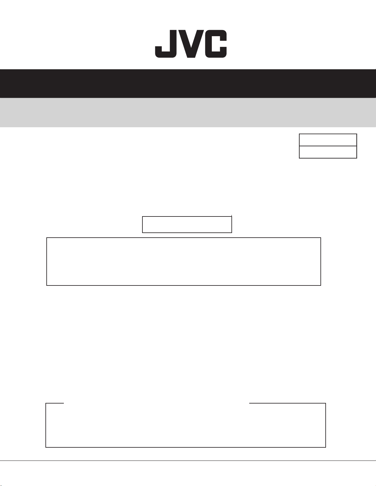
■CONFIRMING MODEL NAME, SERIAL NUMBER, ID NUMBER AND CODE NUMBER
NOTE : The panel's ID number is used when you reference the characteristic voltage value of the panel
on web site.
Voltage and CODE No.
SERIAL NO.
301201327
Vd=60V
Vs=180V
CODE AA-01
For example
CODE : AA
Model name and serial No.
NEC NP35B2MF01AA
301201327
*********************
*********************
*********************
For example
Model : NP35B2MF01AA
Serial No. : 301201327 (9 figures)
■MAIN PARTS LOCATION
COMMON PWB
Flexible cable
Common-side A
Flexible cable
Common-side B
COMMON BRANCH PWB
SCAN RELAY PWB
HIGH VOLTAGE
PWB
PANEL ID No.
222212260043
(12 figures)
Flexible cable
Scan-side A
Flexible cable
Scan-side B
Flexible cable
Common-side C
2(No.52091D)
DIGITAL PWB
SIGNAL RELAY PWB (left) SIGNAL RELAY PWB (right)
Heat-sink
A B C D E F G H I
Flexible cable
Scan-side C
Flexible cable
Scan-side D
J
Page 3
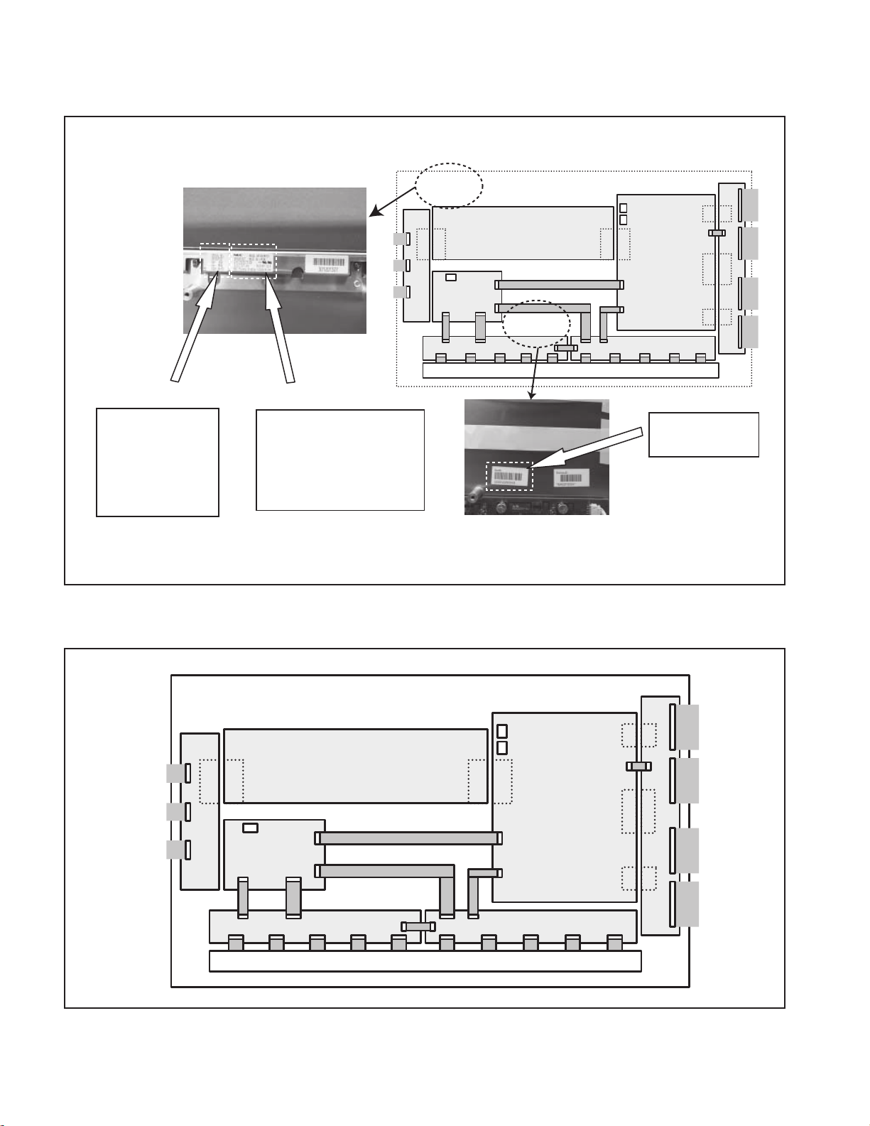
■INSPECTION OF COMPONENTS ON THE PW BOARD
Diagnose the PW board in PDP unit by checking defects based on the following items.
1. Inspection of fuses
Measure the resistance of each fuse with a circuit tester, and check OK or NG.
1.1 Glass fuses (F301, F307) on the HIGH VOLTAGE PWB 1.2 Chip fuse (FU701) on the DIGITAL PWB
TP307
F303
F301
1.3 Fuse resistances (R10, R4, R6) and chip fuse (R20)
on the HIGH VOLTAGE PWB
OK: Short
NG: Open
In case of F303, check
between the pin 6 (or
pin 7) of CN303 and
TP307.
R10
OK: Approx. 2.2Ω
NG: Open
R4
R10
R6
R4
OK: Approx. 2.2Ω
NG: Open
R6
OK: Approx. 2.2Ω
R20
NG: Open
R20
OK: Approx. 10Ω
NG: Open
FU701
OK: Short
NG: Open
1.4 Fuse resistance (R7) and chip fuse (R9) on the
HIGH VOLTAGE PWB
R7
R7
OK: Approx. 2.2Ω
NG: Open
R9
R9
OK: Approx. 10Ω
NG: Open
R1
R1
OK: Approx. 2.2Ω
NG: Open
1.6 Fuse resistances (R2, R3) on the HIGH VOLTAGE PWB1.5 Fuse resistance (R1) on the HIGH VOLTAGE PWB
R3
R2
OK: Approx. 2.2Ω
NG: Open
R3
OK: Approx. 2.2Ω
R2
NG: Open
(No.52091D)3
Page 4
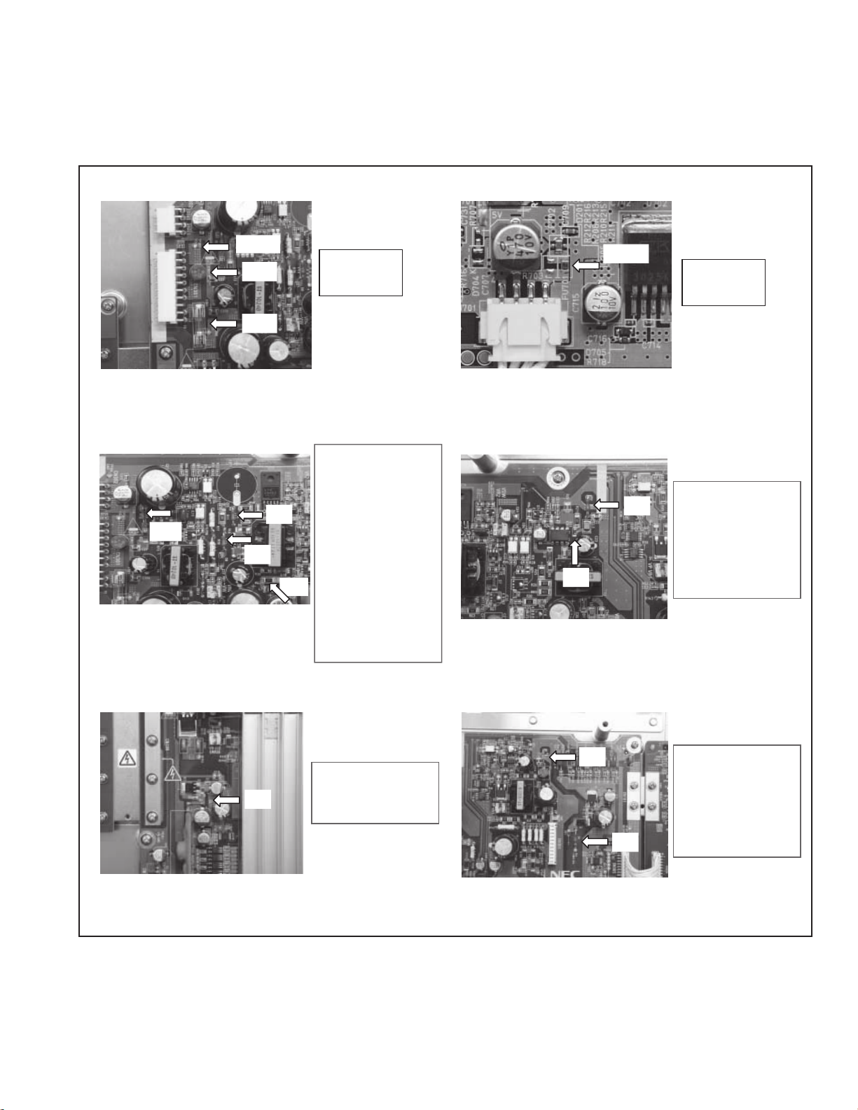
2. Inspection of data ICs
According to the following procedures, measure with a circuit tester and check OK or NG.
Check the pin 5 or pin 6 of the connector [CN11] on the SIGNAL RELAY PWB (right).
OK: Open
NG: Short
Detach the connector [CN11] on the SIGNAL RELAY PWB (right) and check the conduction between the pin 5 (or
pin 6) and the ground.
In case of "short", one of the data ICs connecting the signal relay board may be defective, and you should check
whether there is any trace of damage on the data IC's surface after removing the heat-sink on the data IC.
3. Inspection of power IC
According to the following procedures, measure with a circuit tester and check OK or NG.
The allocation of power IC to be checked is shown below.
HIGH VOLTAGE PWB
PH2201N
4(No.52091D)
Page 5

3.1 PH2201N on the HIGH VOLTAGE PWB
Turn over the board and check each point of power IC as shown below.
R
Q
P
PH2201N
A
B
C
D
E
F
G
H
I
J
K
L
M
N
Check point
Between
A - B
A - R
B - C
B - H
B - J
B - K
Between
C - J
E - F
F - G
F - R
G - L
H - Q
Between
I - J
I - Q
M - Q
N - Q
O - Q
OK: Over 1kΩ
NG: Short
R
A
B
C
D
E
F
G
PH2201N
H
I
J
K
L
Q
M
N
P
O
4. Inspection of scan IC drivers
According to the following procedures, measure with a circuit tester and check OK or NG.
4.1 Scan IC driver on the SCAN RELAY PWB
NEGA
Check point
Between NEGA - POSI
POSI
OK: Over 1kΩ
NG: Short
NEGA
(No.52091D)5
Page 6

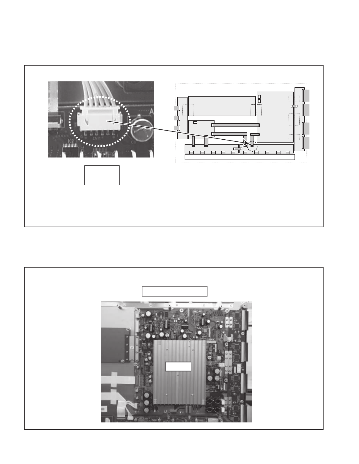
■DISASSEMBLY PROCEDURE
1. Removing the COMMON PWB
(1) Detach the 3 connectors.
(2) Remove the 8 screws [A].
(3) Remove the COMMON PWB.
(1) Detach the 8 connectors.
(2) Remove the 5 screws [D].
(3) Remove the SIGNAL RELAY PWB (left).
2. Removing the DIGITAL PWB
(1) Detach the 4 connectors.
(2) Remove the 6 screws [B].
(3) Remove the DIGITAL PWB.
3. Removing the HIGH VOLTAGE PWB
(1) Detach the 3 connectors.
(2) Remove the 22 screws [C].
(3) Remove the HIGH VOLTAGE PWB.
4. Removing the SIGNAL RELAY PWB (left)
Note : Removing the heat-sink in advance
is required. Refer to the following page
to remove the heat-sink.
COMMON PWB
A
COMMON BRANCH PWB
5. Removing the SIGNAL RELAY PWB (right)
(1) Detach the 8 connectors.
(2) Remove the 4 screws [E].
(3) Remove the SIGNAL RELAY PWB (right).
6. Removing the SCAN RELAY PWB
(1) Detach the 5 connectors.
(2) Remove the 10 screws [F].
(3) Remove the SCAN RELAY PWB.
C
SCAN RELAY PWB
F
B
DIGITAL PWB
E
D
: connector
SIGNAL RELAY PWB (left)
Note : Check the state of the detached cables and connectors.
(1) Check any dirt or peeling in the contact part of the flat cable, and any crack, crease, disconnection
and short-circuit of wires.
(2) Check any foreign substance in the connector's contact .
(3) Check the state of plugging the flat cable into the connector, and confirm it locks completely.
HIGH VOLTAGE
PWB
Heat-sink
SIGNAL RELAY PWB (right)
G
6(No.52091D)
Page 7

heat-sink
silicone and PC
appearance of
separation jig
separation jig
TCP
REMOVING THE HEAT SINK
(1) Remove the 7 screws [G] shown in the previous
page.
(2) With a hot air blower, carry out eliminary heating
of the whole heat- sink. The temperature of the
heat-sink and surrounding parts should not
exceed 100
(3) Remove the heat-sink from TCP by inserting the
separation jig in the crevice between the heat-sink
and TCP, heating the heat-sink with a hot air
blower sequentially from an end.
℃.
hot air blower
Fig.1
Fig.2
separation jig
(4) Insert the separation jig sequentially from an end
of the heat-sink and separate it.
Note :
(1) The silicone sheet is stuck on the back
of the heat-sink, and if you tear it off
forcibly, damaging the data TCP tips
may be caused.
(2) Do not give stress to the fin of the heat sink and data TCP.
(3) The heat-sink cannot be re-used, when
the silicone (gray color) of the heat-sink
is damaged and PC (phase change :
white) is exposed.
Fig.3
(No.52091D)7
Page 8

■CONFIRMING REFERENCE VOLTAGE
Each PDP panel has the characteristic voltage value.
In the adjustment after fix or exchange of a PW board,
this voltage value is used as reference.
You can get it from the vendor's web site on the Internet.
1. Getting the characteristic voltage value of the PDP panel
1.1 Access the following address by the Web browser of
your PC.
http://203.126.119.92/necpd/
1.2 After [NEC-ITLS] screen is displayed, click "Click here
to log on to NPD". (Fig. 1)
1.3 Type the following user name and password into the
dialog box and click "Enter" button. (Fig. 2)
Username: JVCJPN01
Password: jvckoseki (lower-case)
1.4 After [WELCOME TO NEC-ITLS] is displayed (Fig. 3),
click the "Voltage" icon in the "Enquiry" holder on the
upper left part of the window. (Fig. 4)
1.5 After [VOLTAGE ENQUIRY] is displayed (Fig. 5), enter
the panel ID number, which is shown on the panel
(refer to page 2), into the dialog box and click "GO".
Fig. 1
1.6 Then, the characteristic voltage value will be displayed.
(Fig. 6)
Fig. 5
Fig. 2
Fig. 3
8(No.52091D)
Fig. 6
Fig. 4
Page 9

■ADJUSTMENTS
Item
Vbw / -Vw
VOLTAGE
ADJUSTMENT
Measuring
instrument
Test point
DC voltmeter TP (Vbw)
TP (-Vw)
GND
[HIGH VOLTAGE
PWB]
VR4(-Vw)
Adjustment part Description
VR3 (Vbw)
VR4 (-Vw)
[HIGH VOLTAGE
PWB]
(1) Measure the voltage between TP(-Vw) and
TP(Vbw) on the HIGH VOLTAGE PWB.
(2) Adjust the voltage same as the reference
data of Vbw shown in web site by VR3.
※The adjustment accuracy is within ±0.5V.
(3) Measure the voltage between TP(-Vw) and
GND on the HIGH VOLTAGE PWB.
(4) Adjust the voltage same as the reference
data of -Vw shown in web site by VR4.
※The adjustment accuracy is within ±0.5V.
Vsw / Vp
VOLTAGE
ADJUSTMENT
TP(-Vw)
DC voltmeter TP (Vp)
TP (Vsw)
GND
[HIGH VOLTAGE
PWB]
VR2(Vsw)
VR1 (Vp)
VR2 (Vsw)
[HIGH VOLTAGE
PWB]
VR3 (Vbw)
TP(Vbw)
(1) Measure the voltage between TP(Vsw) and
GND on the HIGH VOLTAGE PWB
.
(2) Adjust the voltage same as the reference
data of Vsw shown in web site by VR2.
※The adjustment accuracy is within
±0.5V.
(3) Measure the voltage between TP(Vp) and
GND on the HIGH VOLTAGE PWB
.
(4) Adjust the voltage same as the reference
data of Vp shown in web site by VR1.
※The adjustment accuracy is within
VR1 (Vp)
TP(Vp)
±1.5V.
TP(Vsw)
(No.52091D)9
Page 10

■PARTS LIST
2
PDP UNIT
3
6
1
5
A B C D E F G H I
Heat-sink
5 6
NOTE : (1)Please check a code number with the seal stuck on the rear side
of the PDP panel.
(2)Version is indicated by the seal stuck on each PW board.
Ref No. Parts No.
1
2
3
4
5
6
7
CODE
AA, BA
AA, BA
AA, BA
AA, BA
AA, BA
AA, BA
AA
BA
Version
01E
01C
01A
01A
01B
01B
02E-10
01D-10
NE-9S899437
NE-9S899376
NE-9S899594
NE-9S899382
NE-9S899510
NE-9S899492
NE-9S899276
NE-9S899281
Parts name Description
HIGH VOLTAGE PWB
SCAN RELAY PWB
COMMON BRANCH PWB
COMMON PWB
SIGNAL RELAY PWB
SIGNAL RELAY PWB
DIGITAL PWB
J
(left
)
(right)
01A
FK2600686
The written example of
the seal on a PWB
Indication of Version
10(No.52091D)
NOTES AT THE TIME OF PW BOARD EXCHANGE
It will become the cause of failure if dust adheres to the inside of a connector, or a flat wire and
a point-of-contact part.
When the PW board is exchanged, be careful of the dust and dirt of the inside of a connector, or
a flat wire and a point-of-contact part enough.
Page 11

(No.52091D)11
Page 12

Victor Company of Japan, Limited
AV & MULTIMEDIA COMPANY VIDEO DISPLAY CATEGORY 12, 3-chome, Moriya-cho, kanagawa-ku, Yokohama, kanagawa-prefecture, 221-8528, Japan
(No.52091D)
Printed in Japan
WP
C
 Loading...