

Page 1
SERVICE MANUAL
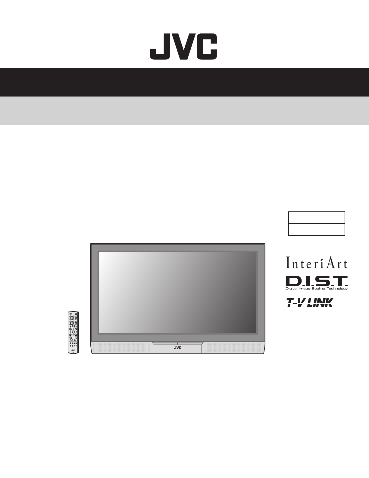
PDP COLOUR TELEVISION
PD-35B50BJ, PD-35B50BU PD-42B50BJ, PD-42B50BU
BASIC C
FP2
HASSIS
1 PRECAUTION
2 SPECIFIC SERVICE INSTRUCTIONS
3 DISASSEMBLY
4 ADJUSTMENT
5 TROUBLESHOOTING
......................................................................................................................................................... 1-4
..................................................................................................................................................... 1-16
...................................................................................................................................................... 1-33
........................................................................................................................................... 1-48
COPYRIGHT © 2004 Victor Company of Japan, Limited
TABLE OF CONTENTS
...................................................................................................................... 1-8
No.YA098
2004/6
Page 2
SPECIFICATION
Contents
Items
Dimensions (W x H x D)
Mass 38.3kg 30.4kg
TV RF System CCIR B / G, I, D / K, L
Colour System RF PAL / SECAM
Stereo System A2 (B / G, D / K), NICAM (B / G, I, D / K, L)
Teletext System FLOF (Fastext), TOP, WST (World Standard System)
Receiving Frequency VHF 47MHz ~ 470MHz
Intermediate Frequency VIF 38.9MHz (B / G, I, D / K, L)
Colour Sub Carrier Frequency
Power Input AC110V ~ AC240V, 50Hz
Power Consumption Operate : 303W, Stand by: 3.0W Operate : 244W, Stand by : 3.0W
Plasma Display Panel (PDP) QLE0028-001 QLE0021-002
Screen Size Visible size : 107.5cm (Diagonel) / Visible size : 91.0cm (Diagonel) /
Display Pixels
Speaker 6.6cm round x4
Audio Power Output 10W + 10W (Oblique cone)
Aerial Input Teminal 75Ω unbalanced, coaxial
External EXT-1 (Input/Output) 21 pin Euro connector (SCART socket)
terminal
EXT-2 (Input/Output) 21 pin Euro connector (SCART socket)
EXT-3 (Input) 21 pin Euro connector (SCART socket)
EXT-4 (Input) COMPONENT VIDEO RCA pin jack x 3
1125i / 750p Y : 1V(p-p), Sync
525i / 525p / 625i / 625p
AUDIO 500mV (rms), High impedance, RCA pin jack x 2
EXT-5 (Input) S-VIDEO Mini-DIN 4 pin x 1
VIDEO 1V(p-p), Positive (Negative sync provided), 75Ω, RCA pin jack x 1
AUDIO 500mV (rms), Low impedance, RCA pin jack x 2
AUDIO OUTPUT (Fixed) 500mV (rms), Low impedance, RCA pin jack x 2
Subwoofur OUTPUT 500mV (rms), Low impedance, RCA pin jack x 1
CENTRE CH INPUT 500mV (rms), Low impedance, RCA pin jack x 1
PC (RGB) INPUT D-sub 15pin x 1
Headphone 3.5mm Stereo mini jack x 1
Remote Control Unit RM-C1811H (AA/R6 TYPE battery x 2)
Design & specifications are subject to change without notice.
1-2 (No.YA098)
104.5cm x 72.9cm x 11.0cm 90.7cm x 63.4cm x 11.7cm
EXT PAL / SECAM / NTSC3.58 / NTSC4.43
UHF 470MHz ~ 862MHz
CATV 116MHz ~ 172MHz, 220MHz ~ 469MHz
SIF
33.4MHz (5.5MHz: B / G) / 32.9MHz (6.0MHz: I) / 32.4MHz (6.5MHz: D / K) /
40.45MHz (6.5MHz :L)
PAL : 4.43MHz
SECAM : 4.40MHz / 4.25MHz
NTSC : 3.58MHz / 4.43MHz
42V wide aspect (16:9) 35V wide aspect (16:9)
93.3 cm x 53.3 cm (H x V) 78.6 cm x 44.2 cm (H x V)
H: 852 pixels / V: 480 pixels H: 853 pixels / V: 480 pixels
[W-VGA] [W-VGA]
• Video input, S-video (Y / C) input, Audio L / R inputs and RGB inputs
are available.
•
TV broadcast outputs (Video and Audio L / R) are available.
•
Video input, S-video (Y / C) input, Audio L / R inputs and RGB inputs
are available.
•
Video and Audio L / R outputs are available.
•
T-V LINK functions are available.
•
Video input and Audio L / R inputs are available.
Pb/Pr : ±0.35V(p-p), 75
Y : 1V(p-p), Positive (Negative sync prorided), 75
Cb/Cr :
Y : 1V(p-p), Positive (Negative sync provided), 75
C : 0.286V(p-p) (Burst signal), 75
R/G/B : 0.7V (p-p), 75
HD / VD : 1V (p-p) ~ 5V (p-p), High impedance
Available signal
VGA : 640 pixels x 480 pixels (Horizontal : 31.5kHz / Vertical : 60Hz)
PD-42B50BJ PD-35B50BJ
PD-42B50BU PD-35B50BU
0.7
V(p-p), 75
±0.35V(p-p) terminal x3
Ω
Ω
Ω
, 75
Ω
Ω
Ω
Ω
Page 3
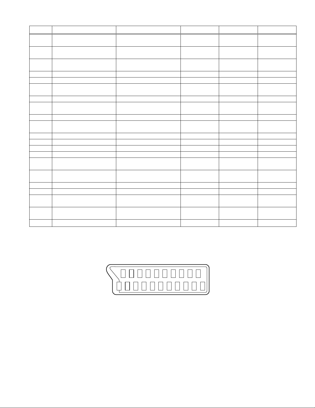
21-pin Euro connector (SCART) : EXT-1/EXT-2/EXT-3
PinNo. Signal designation Matching value EXT-1 EXT-2 EXT-3
AUDIO R output
1
500mV(rms) (Nominal),
Used (TV OUT)
Used (LINE OUT)
Not used
Low impedance
2
AUDIO R input
500mV(rms) (Nominal),
Used
Used
Used
High impedance
3
AUDIO L output
500mV(rms) (Nominal),
Used (TV OUT)
Used (LINE OUT)
Not used
Low impedance
4
5
6
AUDIO GND
GND (B)
AUDIO L input
500mV(rms) (Nominal),
Used
Used
Used
Used
Used
Used
Used
Used
Used
High impedance
7
8
9
10
B input
FUNCTION SW
(SLOW SW)
GND (G)
SCL / T-V LINK
700mV(
B-W
), 75Ω
Low : 0V-3V, High : 8V-12V,
High impedance
Used
Used
Used
Not used
Used
Used
Used
Used
Not used
Used
Used
Not used
(SCL2/TV-LINK)
11
12
13
14
15
G input
SDA
GND (R)
GND (YS)
R / C input
700mV(
B-W
R : 700mV(
), 75Ω
B-W
), 75Ω
Used
Not used
Used
Used
Used (C1/R)
Used
Used(SDA2)
Used
Not used
Used (C2/R)
Not used
Not used
Used
Not used
Not used
C : 300mV(p-p), 75Ω
16
17
18
19
Ys input
(FAST SW)
GND (VIDEO output)
GND (VIDEO input)
VIDEO output
Low : 0V-0.4V
High : 1V-3V, 75Ω
1V(p-p) (Negative going sync),
Used
Used
Used
Used (TV OUT)
Used
Used
Used
Used (LINE OUT)
Not used
Used
Used
Not used
75Ω
20
VIDEO / Y input
1V(p-p) (Negative going sync),
Used
Used
Used
75Ω
21
COMMON GND
Used
Used
Used
(P-P= Peak to Peak, B-W= Blanking to white peak)
[Pin assignment]
20 18 16 14 12 10 8 6 4 2
21 19 17 15 13 11 9 7 5 3 1
(No.YA098) 1-3
Page 4

D
SECTION 1
PRECAUTION
1.1 SAFETY PRECAUTIONS [EXCEPT FOR UK]
(1) The design of this product contains special hardware,
many circuits and components specially for safety
purposes. For continued protection, no changes should
be made to the original design unless authorized in writing
by the manufacturer. Replacement parts must be identical
to those used in the original circuits. Service should be
performed by qualified personnel only.
(2) Alterations of the design or circuitry of the products should
not be made. Any design alterations or additions will void
the manufacturer's warranty and will further relieve the
manufacturer of responsibility for personal injury or
property damage resulting therefrom.
(3) Many electrical and mechanical parts in the products have
special safety-related characteristics. These
characteristics are often not evident from visual inspection
nor can the protection afforded by them necessarily be
obtained by using replacement components rated for
higher voltage, wattage, etc. Replacement parts which
have these special safety characteristics are identified in
the parts list of Service manual. Electrical components
having such features are identified by shading on the
schematics and by () on the parts list in Service
manual. The use of a substitute replacement which does
not have the same safety characteristics as the
recommended replacement part shown in the parts list
of Service manual may cause shock, fire, or other hazards.
(4) Don't short between the LIVE side ground and ISOLATED
(NEUTRAL) side ground or EARTH side ground when
repairing.
Some model's power circuit is partly different in the GND.
The difference of the GND is shown by the LIVE : (
GND, the ISOLATED (NEUTRAL) : (
EARTH : (
) side GND. Don't short between the LIVE
) side GND and
side GND and ISOLATED (NEUTRAL) side GND or EARTH
side GND and never measure the LIVE side GND and
ISOLATED (NEUTRAL) side GND or EARTH side GND at
the same time with a measuring apparatus (oscilloscope
etc.).If above note will not be kept, a fuse or any parts will
be broken.
(5) If any repair has been made to the chassis, it is
recommended that the PDP POWER SUPPLY setting
should be checked or adjusted.
(6) The high voltage applied to the PDP must conform with
that specified in Service manual. Excessive high voltage
can cause an increase in arcing and possible component
damage, therefore operation under excessive high voltage
conditions should be kept to a minimum, or should be
prevented. If severe arcing occurs, remove the AC power
immediately and determine the cause by visual inspection
(incorrect installation, cracked or melted high voltage
harness, poor soldering, etc.). To maintain the proper
components in the circuitry including the PDP must be
the exact replacements or alternatives approved by the
manufacturer of the complete product.
(7) Do not check high voltage by drawing an arc. Use a high
voltage meter or a high voltage probe with a VTVM.
Discharge the picture tube before attempting meter
connection, by connecting a clip lead to the ground frame
and connecting the other end of the lead through a 10kΩ
2W resistor to the anode button.
) side
(8) When service is required, observe the original lead dress.
Extra precaution should be given to assure correct lead
dress in the high voltage circuit area. Where a short circuit
has occurred, those components that indicate evidence
of overheating should be replaced. Always use the
manufacturer's replacement components.
(9) Isolation Check
(Safety for Electrical Shock Hazard)
After re-assembling the product, always perform an
isolation check on the exposed metal parts of the cabinet
(antenna terminals, video/audio input and output
terminals, Control knobs, metal cabinet, screw heads,
earphone jack, control shafts, etc.) to be sure the product
is safe to operate without danger of electrical shock.
a) Dielectric Strength Test
The isolation between the AC primary circuit and all metal
parts exposed to the user, particularly any exposed metal
part having a return path to the chassis should withstand
a voltage of 3000V AC (r.m.s.) for a period of one second.
(. . . . Withstand a voltage of 1100V AC (r.m.s.) to an
appliance rated up to 120V, and 3000V AC (r.m.s.) to an
appliance rated 200V or more, for a period of one second.)
This method of test requires a test equipment not generally
found in the service trade.
b) Leakage Current Check
Plug the AC line cord directly into the AC outlet (do not use
a line isolation transformer during this check.). Using a
"Leakage Current Tester", measure the leakage current
from each exposed metal part of the cabinet, particularly
any exposed metal part having a return path to the chassis,
to a known good earth ground (water pipe, etc.). Any
leakage current must not exceed 0.5mA AC (r.m.s.).
However, in tropical area, this must not exceed 0.2mA AC
(r.m.s.).
Alternative Check Method
Plug the AC line cord directly into the AC outlet (do not
use a line isolation transformer during this check.).
Use an AC voltmeter having 1000 ohms per volt or
more sensitivity in the following manner. Connect a
1500Ω 10W resistor paralleled by a 0.15µF AC-type
capacitor between an exposed metal part and a known
good earth ground (water pipe, etc.). Measure the AC
voltage across the resistor with the AC voltmeter. Move
the resistor connection to each exposed metal part,
particularly any exposed metal part having a return path
to the chassis, and measure the AC voltage across
the resistor. Now, reverse the plug in the AC outlet and
repeat each measurement. Any voltage measured
must not exceed 0.75V AC (r.m.s.). This corresponds
to 0.5mA AC (r.m.s.).
However, in tropical area, this must not exceed 0.3V AC
(r.m.s.). This corresponds to 0.2mA AC (r.m.s.).
AC VOLTMETER
(HAVING 1000Ω/V,
OR MORE SENSITIVITY)
0.15µF AC-TYPE
PLACE THIS PROBE
1500Ω 10W
GOOD EARTH GROUND
ON EACH EXPOSE
ME TA L PA RT
1-4 (No.YA098)
Page 5

1. 2 SAFETY PRECAUTIONS [FOR UK]
(1) The design of this product contains special hardware and many circuits and components specially designed for safety
purposes. For continued protection, no changes should be made to the original design unless authorized in writing by the
manufacturer. Replacement parts must be identical to those used in the original circuits. Service should be performed by
qualified personnel only.
(2) Alterations of the design or circuitry of the product should not be made. Any design alterations or additions will void the
manufacturer's warranty and may result in personal injury or property damage resulting therefrom.
(3) Many electrical and mechanical parts in the product have special safety-related characteristics. These characteristics are
often not evident from visual inspection nor can the protection afforded by them necessary be obtained by using replacement
components rated for higher voltage, wattage, etc. Replacement parts which have these special safety characteristics are
identified in the Parts List of Service Manual. Electrical components having such features are identified by shading on the
schematics and by ( ) on the Parts List in the Service Manual. The use of a substitute replacement which does not have the
same safety characteristics as the recommended replacement part shown in the Parts List of Service Manual may cause
shock, fire, or other hazards.
(4) The leads in the products are routed and dressed with ties, clamps, tubings, barriers and the like to be separated from live
parts, high temperature parts, moving parts and / or sharp edges for the prevention of electric shock and fire hazard. When
service is required, the original lead routing and dress should be observed, and it should be confirmed that they have been
returned to normal, after re-assembling.
WARNING
(1) The equipment has been designed and manufactured to meet international safety standards.
(2) It is the legal responsibility of the repairer to ensure that these safety standards are maintained.
(3) Repairs must be made in accordance with the relevant safety standards.
(4) It is essential that safety critical components are replaced by approved parts.
(5) If mains voltage selector is provided, check setting for local voltage.
(No.YA098) 1-5
Page 6
1.3 INSTALLATION
1.3.1 HEAT DISSIPATION
If the heat dissipation vent behind this unit is blocked, cooling
efficiency may deteriorate and temperature inside the unit will
rise. The temperature sensor that protects the unit will be
activated when internal temperature exceeds the predetermined level and power will be turned off automatically.
Therefore, please make sure pay attention not to block the heat
dissipation vent as well as the ventilation outlet behind the unit
and ensure that there is room for ventilation around it.
SPACE REQUIRED FOR INSTALLATION
1.3.2 INSTALLATION REQUIREMENTS
Ensure that the minimal distance is maintained, as specified
below, between the unit with and the surrounding walls, as well
as the floor etc.
Install the unit on stable flooring or stands.
Take precautionary measures to prevent the unit from tipping in
order to protect against accidents and earthquakes.
150 mm or
150 mm
more
200 mm or
200 mm
more
50 mm
50 mm or more
1.3.3 FALL TIP PREVENTION MEASURES
Take precautionary measures to prevent the unit from falling or
tipping to protect against emergencies such as earthquakes as
well as accidents.
Fasten the supplied hook for tip fall prevention using the screws,
also supplied, behind the display unit, and use them together
with durable cords (to be purchased separately) to secure the
unit to a robust part such as the wall surface or pillars.
150 mm
or more
150 mm
200 mm
200 mm
or more
50 mm
50 mm or more
1-6 (No.YA098)
The supplied hook for tipfall prevention
Page 7

1. 4 PRECAUTIONS REGARDING PDP
1.4.1 PRECAUTIONS DURING NOTES FOR TRANSPORTATION
When transporting the unit, pressure exerted on the internal
PDP (Plasma Display Panel) due to improper handling (such
as tossing and dropping) may cause damages even when the
unit is carefully packed. To prevent accidents from occurring
during transportation, pay careful attention prior to delivery such
as through explaining the handling instructions to transporters.
Ensure that the following requirements are met during
transportation, as the PDP of this unit is made of glass and
therefore fragile:
(1) Avoid vibrations and impacts
The unit may be broken if it is toppled sideways even
when properly packed. Ensure that the unit is carried by at
least 2 persons and pay careful attention not to exert any
vibration or impact on it.
(2) Do not place equipment horizontally
Ensure that it is placed upright and not horizontally during
transportation and storage as the PDP is very vulnerable
to lateral impacts and may break easily under such
circumstances.
During transportation, ensure that the unit is loaded along
the traveling direction of travel of the vehicle, and avoid
stacking them on one another.
For storage, ensure that they are stacked in 2 layers or
less even when placed upright.
1.4.2 RESIDUAL IMAGE / BURN-IN ON SCREEN
Like CRTs, “burn-in” may occur when a same image is
continuously displayed over an extended period of time.
As this may also shorten the life span of the PDP. Therefore, turn
off the display when not in use, scroll the screen, make use
of screen-savers, or allow even distribution on the display by
inverting the brightness, switching to complementary colors or
inserting animated images at periodic intervals.
As burn-in is more likely to occur with high brightness and contrast
settings, try to use neutral gradations or medium tone colors.
Burn-in does not occur in the case of animated images.
When switching to another image after continuous display of
the previous image, residual images may become prominent,
as luminance in a part of the display is higher than the other
parts.
This is not a defect but is because due to the discharge surface
of the lighted portion has become being relatively activated and
its luminance higher than the unlighted parts.
1.4.4 OPTICAL FILER (PANEL FILTER)
Avoid placing the unit under direct sunlight over a prolonged
period of time. This may cause the optical filter to deteriorate in
quality and color.
Clean the filter surface by wiping it softly lightly with outing flannels
a soft and lightly fuzz cloth (such as flannel).
Do not use solvents such as benzine or thinner to wipe the filter
surface. This may cause the filter to deteriorate in quality or the
coating on the surface to come off.
As the filter surface is fragile., do not scratch or hit it with hard
materials.
1.4.5 NOTES PRECAUTIONS FOR REPLACEMENT OF
EXTERIOR PARTS
Take note of the following when replacing exterior parts (back
REAR COVER, FRONT PANEL, optical filter)
• Do not exert pressure on the front of the PDP (glass surface).
• Pay careful attention not to scratch or stain the front of the PDP
(surface) with hands.
• When replacing exterior parts, the front of the PDP should be
placed facing downward. Place a mat, etc. underneath to avoid
causing scratches to the front surface. However, never use
materials that are too soft (such as blanket cloth). If
replacement is made with the PDP surface facing downward
and in contact with the blanket, pressure may be exerted on
the PDP, thus causing damages to it.
1.4.3 INFRARED RAYS
Near Near-infrared rays (800nm to 1000nm) are emitted from
the front of the panel, and this may give rise to malfunctions in
infrared remote controls or communication systems placed near
it. In this case, avoid direct infrared rays (and reflected rays in
some cases) from the screen by either changing the direction of
the unit or other infrared systems or securing a longer keeping
a distance from the screen.
(No.YA098) 1-7
Page 8
SECTION 2
SPECIFIC SERVICE INSTRUCTIONS
2.1 FEATURES
2.1.1 HIGH-DEFINITION IMAGE TECHNOLOGY (DIST)
• DIST (Digital Image Scaling Technology)
Employs an interpolation method that doubles the scanning
lines to realize 480-line flickerfree picture making it especially
suitable for reproducing high-resolution pictures even on largescreen displays.
2.1.2 MAIN FUNCTION
•
DIGITAL VNR
The DIGITAL VNR function cuts down the amount of noise in
original picture. There are three function settings of AUTO,MIN
and MAX.
• Super DigiPure
This function uses the latest technology to give viewer a natural
looking picture.
It consist of DigiPure and picture motion compensation function.
•
MOVIE THEATRE
This function displays a cinema film picture more smoothly
and naturally on the screen.
•
COLOUR MANAGEMENT
This function ensures dull colours are compensated to produce
natural hues.
• Sleep Timer
Setting for situations such as falling asleep while watching TV,
and for prevention against forgetting to turn off the TV. The
power supply of the TV will be cut off automatically when the
time exceeds the set up timing (maximum 2 hours).
• 3D SOUND function
This function makes the speaker sounds like in a wider
ambience.
• Teletext function
The teletext broadcast can be viewed and the teletext pages
can be stored in memory.
• T-V LINK function
This function make a VCR could automatically download the
data or image from the TV, and turn on the TV to view the image
when it playing.
2.1.3 ASPECT CONTROL
The screen size can be changed according to the picture aspect
ratio.
• ZOOM function
Desired screen size (AUTO/REGULAR / PANORAMIC / 14:9
ZOOM / 16:9 ZOOM / 16:9 ZOOM SUBTITLE / FULL) can be
selected.
2.1.4 MULTI-SCREEN FUNCTION
• Twin-pictures function
With the function, two pictures can be displayed at the Twin
pictures mode.
• Multi-picture function
With this function, one of multi-picture (12 pictures) can be
displayed at the same time.
• Freeze function
The images that are currently seen can be viewed on the memo
screen (still picture).
It is convenient for taking down notes like application address
and recipe of cooking program etc, while enjoying the current
program.
2. 2 MAIN DIFFERENCE LIST
Item
TABLE TOP STAND
WALL BRACKET NO YES
1-8 (No.YA098)
PD-42B50BJ PD-42B50BU
PD-35B50BJ PD-35B50BU
YES NO
Page 9
2. 3 TECHNICAL INFORMATION
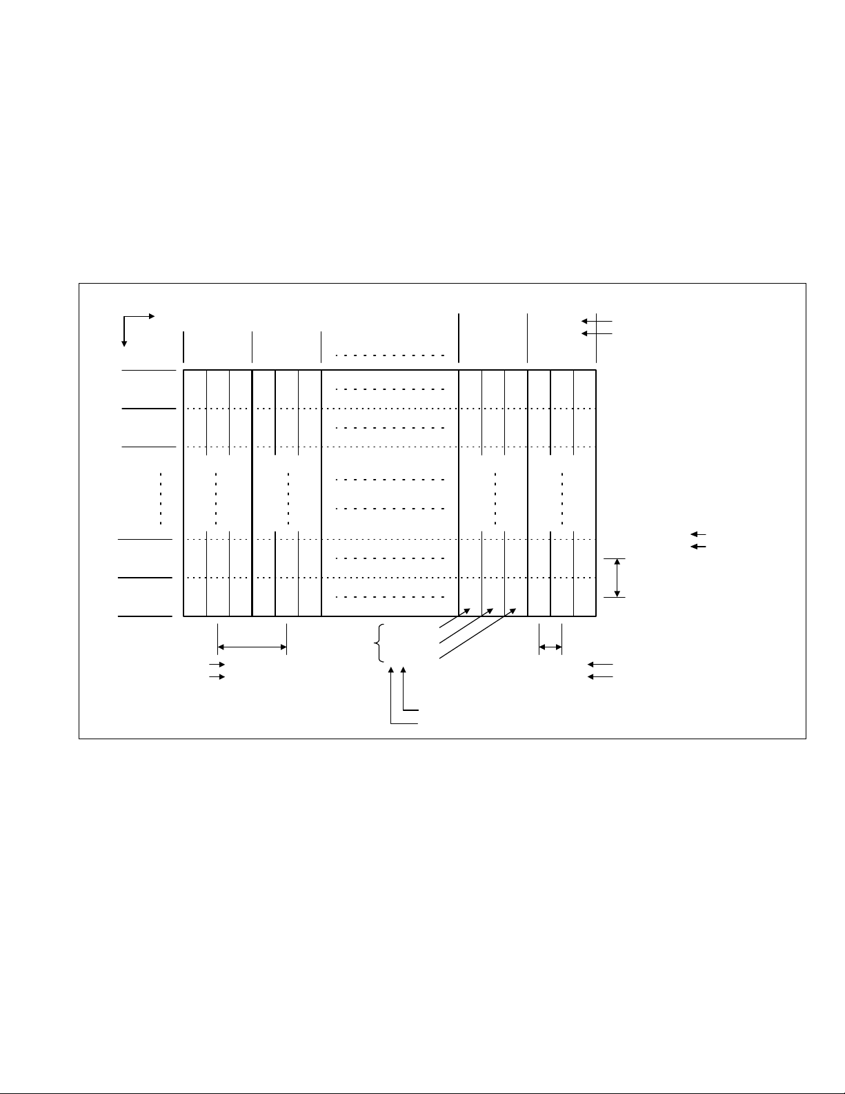
2.3.1 PDP STRUCTURE AND CHARACTERISTIC
This unit uses the flat type panel PDP (Plasma Display Panel), instead of the conventional CRT (Cathode Ray Tube),
as a display unit.
2.3.1.1 PIXEL (CELL) ARRAY
PDP is constructed by sealing the xenon, which emits neon and ultraviolet rays for discharging purpose, in between the electrodes
lay on the front glass substrate and rear glass substrate.
One pixel is composed of 3 RGB cells, with cell pitch of 0.365mm (1 pixel 1.095mm) [42V MODEL] / 0.307 mm (1 plxel 0.921 mm)
[35V MODEL] horizontally and 1.110mm [42V MODEL] / 0.921 mm [35V MODEL] vertically.
The cell is arrayed in each RGB color as shown in Fig. 1. One pixel is formed by interlacing each RGB color cell.
One cell size is 0.365mm [42V MODEL] / 0.307 mm [35V MODEL] horizontally and 1.110mm [42V MODEL] / 0.921 mm [35V MODEL]
vertically.
Direction
Vertically
No.1
Pixel line
No.2
Pixel line
No.479
Pixel line
No.480
Pixel line
42V MODEL
35V MODEL
Horizontally
No.1
Pixel
sequence
No.2
Pixel
sequence
B G R B G R
(R) (B) (R)(G) (G) (B) (R) (B) (R) (B)
BG
(R) (B) (R)(G) (G)
B
(R) (B) (R) (B) (R) (B) (R) (B)
B
(R) (B) (R) (B) (R) (B) (R) (B)
(Horizontally) Pixel pitch
RBGR
(B) (R) (B) (R) (B)
G RBG R
(G) (G)
GRBGR
(G) (G)
1 pixel
(1 dot)
1.095mm
0.921 mm 0.307 mm
B(R) Cell
G(G)
Cell
R(B) Cell
35V MODEL
42V MODEL
No.851 No.852
No.852
Pixel
sequence
B GRBG R
(G) (G)
BGRBGR
(G) (G)
G RBG R
B
(G) (G)
GRBGR
B
(G) (G)
0.365mm
(Horizontally) Cell pitch
No.853
Pixel
sequence
42V MODEL
35V MODEL
1.110 mm 42V MODEL
0.921 mm 35V MODEL
(Vertically)
Pixel pitch
(Cell pitch)
42V MODEL
35V MODEL
Fig.1
2.3.1.2 PIXEL DEFECTS
Though PDP is made by means of ultra precise technology, there are cases whereby not all pixels (cell) will function properly. In
some cases, there may be defective pixels that do not light at all or the ones that always light on.
There are 3 types of Pixel defects, [Bright Dot Defects], [Dark Dot Defects] and [Flicker Dot Defects], as defined respectively in the
following:
(1) Bright Dot Defects
Bright dot defect is a pixel cell that lights though it should not light.
The presence of bright dot defects can be confirmed by inputting a full black signal (pattern).
(2) Dark Dot Defects
Dark dot defect is a pixel cell that does not light, though it should light.
The presence of dark dot defects can be confirmed by inputting a 100% full white signal (pattern).
(3) Flicker Dot Defects
Flicker dot defect is a pixel cell that blinks though it should light or not light.
The presence of flicher dot defects can be confirmed by inputting a full black signal (pattern).
(No.YA098) 1-9
Page 10

2.3.2 MAIN CPU [IC7501] PIN FUNCTION
Pin No. Terminal name Port name I/O Remark
1 TCK TCK I Test purpose
2 TMS TMS I Test purpose
3 TDI TDI I Test purpose
4 TDO TDO O Test purpose
5 NC P2.8 O Not used
6 OSDB0 P2.9 O Bule for OSD
7 OSDB1 P2.10 O Bule for OSD
8 OSDB2 P2.11 O Bule for OSD
9 OSDB3 P2.12 O Bule for OSD
10 OSDB4 P2.13 O Bule for OSD
11 TV-LINK P2.14 I TV-LINK communication
12 RX_BUSY(Sirial) P2.15 O Communication for chassis CPU (Request)
13 VSS33 VSS33 - GND
14 VDD33 VDD33 I 3.3V
15 TV_LINK_OUT P4.5/CS3 O TV-LINK communication
16 A20 P4.4/A20 O Memory (Program ROM) address
17 A19 P4.3/A19 O Memory (Program ROM) address
18 A18 P4.2/A18 O Memory (Program ROM) address
19 A17 P4.1/A17 O Memory (Program ROM) address
20 VSS25 VSS25 - GND
21 VDD25 VDD25 I 2.5V
22 A16 P4.0/A16 O Memory (Program ROM) address
23 A8 A8 O Memory (Program ROM) address
24 A7 A7 O Memory (Program ROM) address
25 A9 A9 O Memory (Program ROM) address
26 A6 A6 O Memory (Program ROM) address
27 A5 A5 O Memory (Program ROM) address
28 A10 A10 O Memory (Program ROM) address
29 A11 A11 O Memory (Program ROM) address
30 A12 A12 O Memory (Program ROM) address
31 VSS33 VSS33 - GND
32 VDD33 VDD33 I 3.3V
33 A4 A4 O Memory (Program ROM) address
34 A3 A3 O Memory (Program ROM) address
35 A2 A2 O Memory (Program ROM) address
36 A1 A1 O Memory (Program ROM) address
37 A0 A0 O Memory (Program ROM) address
38 A13 A13 O Memory (Program ROM) address
39 A14/RAS A14/RAS O Memory (Program ROM) address
40 A15/CAS A15/CAS O Memory (Program ROM) address
41 VSS33 VSS33 - GND
42 VDD33 VDD33 I 3.3V
43 MEMCLK MEMCLK O Clock for memory
44 CSSDRAM CSSDRAM O Chip select for memory
45 CLKEN CLKEN O Clock enable for memory
46 CSROM CSROM O Chip select for memory
47 RD RD O Read for memory
48 UDQM UDQM O Control IN / OUT buffer of memory
49 LDQM LDQM O Control IN / OUT buffer of memory
50 WR WR O Write for memory
51 D15 D15 I/O Data (Program ROM)
52 VSS33 VSS33 - GND
53 VDD33 VDD33 I 3.3V
54 D7 D7 I/O Data (Program ROM)
55 D0 D0 I/O Data (Program ROM)
56 D14 D14 I/O Data (Program ROM)
57 D8 D8 I/O Data (Program ROM)
58 D6 D6 I/O Data (Program ROM)
59 D1 D1 I/O Data (Program ROM)
60 VSS33 VSS33 - GND
61 VDD33 VDD33 I 3.3V
62 D13 D13 I/O Data (Program ROM)
63 D9 D9 I/O Data (Program ROM)
64 D5 D5 I/O Data (Program ROM)
65 D2 D2 I/O Data (Program ROM)
1-10 (No.YA098)
Page 11
Pin No. Terminal name Port name I/O Remark
66 D12 D12 I/O Data (Program ROM)
67 D10 D10 I/O Data (Program ROM)
68 VSS33 VSS33 - GND
69 VDD33 VDD33 I 3.3V
70 D 4 D4 I/O Data (Program ROM)
71 D 3 D3 I/O Data (Program ROM)
72 D11 D11 I/O Data (Program ROM)
73 RSTIN RSTIN I Reset
74 POWER P3.0 O Sleep state release for chassis CPU [Relese : L]
75 ID_TV_POWER(IDTV) P3.1 O Not used
76 REMOCON P3.2 I Remote control
77 PIX CLOCK P3.3 I Clock for OSD
78 OSDR0 P3.4 O Red for OSD
79 OSDR1 P3.5 O Red for OSD
80 OSDR2 P3.6 O Red for OSD
81 OSDR3 P3.7 O Red for OSD
82 MRST(Sirial) P3.8 I/O Communication for chassis CPU (Serial data)
83 MTSR(Sirial) P3.9 I/O Communication for chassis CPU (Serial data)
84 VSS33 VSS33 - GND
85 VDD33 VDD33 I 3.3V
86 VSS25 VSS25 - GND
87 VDD25 VDD25 I 2.5V
88 MICON TX TXD0 I/O Communication for adjustment (Serial data)
89 MICON RX RXD0 I/O Communication for adjustment (Serial data)
90 OSDR4 P3.12 O Red for OSD
91 CLK(Sirial) P3.13 O Communication for chassis CPU (Clock)
92 OSDG0 P3.15 O Green for OSD
93 OSDG1 P5.14 O Green for OSD
94 OSDG2 P5.15 O Green for OSD
95 OSDG3 TRIG_IN O Green for OSD
96 OSDG4 TRIG_OUT O Green for OSD
97 OSDG5 P6.2 O Green for OSD
98 SCL3A P6.3 I/O I2C bus clock (for main memory)
99 SDA3A P6.4 I/O I2C bus Data (for main memory)
100 TEXT / OTHER P6.5 O Teletext signal select [Analog RGB : H Digital RGB : L]
101 IRQ(IDTV) P6.6 O Not used
102 V_PULSE VSYNC I Vertical sync
103 H_PULSE HSYNC I Horizontal sync
104 (COR/RSTOUT) COR/RSTOUT O Not used
105 Ys BLANK/CORBLA O Ys for OSD / Teletext
106 VDD33 VDD33 I 3.3V
107 VSS33 VSS33 - GND
108 XTAL1 XTAL1 I 6MHz for system clock
109 XTAL2 XTAL2 O 6MHz for system clock
110 VSSA VSSA - GN D
111 VDDA VDDA I 2.5V
112 R R O R for OSD / Teletext
113 G G O G for OSD / Teletext
114 B B O B for OSD / Teletext
115 VSSA VSSA - GN D
116 VDDA VDDA I 2.5V
117 CVBS CVBS2 I Video for Teletext
118 VSSA VSSA - GN D
119 VDDA VDDA I 2.5V
120 GND CVBS1B I GND
121 CVBS CVBS1A I Video for Teletext
122 VSSA VSSA - GND
12 3 VDDA VDDA I 2.5V
124 F_KEY_1 P5.0 I Key scan data 1 [ON : H]
125 F_KEY_2 P5.1 I Key scan data 2 [ON : H]
126 POWER_KEY P5.2 I Main power ON / OFF control [ON : L]
127 NC P5.3 I Not used
12 8 (TMODE) TMODE I Test purpose
(No.YA098) 1-11
Page 12

2.3.3 CHASSIS CPU [IC7001] PIN FUNCTION
Pin No. Terminal name Port name I/O Remark
1 NC P60 O Not used
2 P_MU P61 O Viveo mute [Mute : H]
3 FUNC_LED P62 O Not used
4 A_MU P63 O Audio out mute [Mute : H]
5 M_MU P50 O Monitor out mute [Mute : H]
6 PC_SW P51 O PC input switch [ON : H]
7 DIMMER_LED P52 O Power LED brightness control [Low brightness : L]
8 NC P53 O Not used
9 NC P54 O Not used
10 NC P55 O Not used
11 POW_LED P56 O Power LED control [ON : H]
12 NC P57 O Not used
13 SBT2 SBT2 I Communication for main CPU (Clock)
14 SBI2 SBI2 I/O Communication for main CPU (Serial data)
15 SBO2 SBO2 I/O Communication for main CPU (Serial data)
16 REQ P23 O Communication for main CPU (Request)
17 3.3V VDD I 3.3V
18 NC PB0 O Not used
19 GND VSS - GND
20 3.3V XI I 3.3V
21 NC XO O Not used
22 3.3V VDD I 3.3V
23 OSCI OSCI I 16MHz for system clock
24 OSCO OSCO O 16MHz for system clock
25 3.3V (MODE) I 3.3v
26 NC P24 O Not used
27 A92_RST P25 O 3D YC separator reset [Reset : L]
28 NC P26 O Not used
29 LIP_RST P27 O Lip sync reset [Reset : H]
30 NC KI0 O Not used
31 NC KI1 I Not used
32 NC KI2 O Not used
33 MDR_CON P33 I Not used
34 3.3V AVDD I 3.3V
35 NC P34 O Not used
36 DsyncSW2 P35 O Not used
37 NC P36 O Not used
38 NC P37 O Not used
39 HOTPLUG P40 I Not used
40 MECA_SW P41 I Power switch input [ON : L]
41 MAIN_POW P42 O Main power control [ON : L]
42 MSP_RESET P43 O Multi sound processor reset [Reset : H]
43 0V Vref- I GND
44 NC AN4 I Not used
45 AFT1 AN5 I Tuner AFT detection [Detection : H]
46 NC AN6 I Not used
47 NC AN7 I Not used
48 NC P80 O Not used
49 NC P81 O Not used
50 N C TM0IO I Not used
51 N C SBI3 O Not used
52 N C SBO3 I Not used
53 NC P85 O Not used
54 3.3V Vref+ I 3.3V
55 PDP_TX SBI4 O PDP communication for sub CPU
56 PDP_RX SBO4 I PDP communication for sub CPU
57 SDA0 P90 I/O I2C bus data (for chassis memory)
58 SCL0 P91 I/O I2C bus clock (for chassis memory)
59 SDA_DVI P92 I/O Not used
60 SCL_DVI P92 I/O Not used
61 GND AVSS - GND
62 NC AN0 I Not used
63 AGC AN1 I AGC voltage level detection [Detection : H]
64 YS1 AN2 I YS1 detection [Detection : H]
65 YS2 AN3 I YS2 detection [Detection : H]
1-12 (No.YA098)
Page 13
Pin No. Terminal name Port name I/O Remark
66 3.3V VDD I 3.3V
67 NC P70 O Not used
68 NC P71 O Not used
69 NC P72 O Not used
70 NC P73 O Not used
71 NC SBI1 O Not used
72 NC SBO1 O Not used
73 SBD5 * I/O For flash writing
74 SBT5 * I For flash writing
75 3.3V NMI I 3.3V
76 NC IRQ0 I Not used
77 REMOCON IRQ1 I Remote control
78 V_SYNC IRQ2 I Vertical sync
79 WAKEUP_SHM IRQ3 I Sleep state release for chassis CPU [Relese : L]
80 POWERGOOD IRQ4 I Power error detection [Detection : H]
81 REC_LED PA5 O Stand-by power LED control [Stand-by :H]
82 RST RST I Chassis CPU reset [Reset : L]
83 3.3V VDD I 3.3V
84 SCL3A P00 I/O I
85 SDA3A P01 I/O I
86 SCL3B P02 I/O I
2
C bus clock (for 3D separator, colour management / OSD
composition / RGB A-D convert, U / V frontend, sound delay)
2
C bus data (for 3D separator, colour management / OSD
composition / RGB A-D convert, U / V frontend, sound delay)
2
C bus clock (for multi sound process, video / audio select,
colour demod. / sync sep. / RGB SW, 3 line comb filter,
component video / audio select, sync sep. / SW / detect)
2
87 SDA3B P03 I/O I
C bus data (for multi sound process, video / audio select,
colour demod. / sync sep. / RGB SW, component video / audio
select, sync sep. / SW / detect)
88 NC P04 O Not used
89 NC P05 O Not used
90 NC P06 O Not used
91 DVI_RST P07 O Not used
92 GND VSS - GND
93 SCL5055 P10 I/O I2C bus clock (for DIST)
94 NC P11 O Not used
95 SDA5055 P12 I/O I2C bus data (for DIST)
96 NC P13 O Not used
97 NC P14 O Not used
98 15K/OTH P15 O Y signal select for 3D YC separator [525i : H other : L]
99 DsyncSW1 P16 O Not used
100 JCC5057_BUSY P17 I Busy for Colour management / OSD composition [Busy : H]
(No.YA098) 1-13
Page 14

2.3.4 SUB CPU [IC807] PIN FUNCTION [PD-42B50BJ, PD-42B50BU]
Pin No. Terminal name Port name I/O Remark
1 SYSTEM0 PB6/AN6 I PDP size select [1.75V : 42V VGA 3.25V : 35V VGA]
2 SYSTEM3 PB7/AN7 I PDP maker select [0V : SAMSUNG 3.25V : NEC]
3 AVCC AVCC I 5.0V
4 X2 X2 - Not used
5X1 X1 -GND
6 VCL VCL - GND
7 RES RES I Reset [Reset : L]
8 TEST TEST I GND
9 VSS VSS - G ND
10 OSC2 OSC2 O 16MHz for system clock
11 OSC1 OSC1 I 16MHz for system clock
12 VCC VCC I 5.0V
13 PW_LOB P50/WKP0 O Power control [ON : L]
14 PANEL_PW_ON P51/WKP1 O Panel power control [ON : L]
15 TALK_RST P34 O Not used
16 CODEC_RST P35 O Not used
17 I2C_STOP P36 O I2C bus stop control [Stop : L]
18 NC P37 O Not used
19 NC P52/WKP2 O Not used
20 NC P53/WKP3 O Not used
21 NC P54/WKP4 O Not used
22 NC P55/WKP5/ADTRG O Not used
23 SDA1 P10/TMOW I/O I2C bus data (for sub memory)
24 FAN P11/PWM O Not used
25 SCL1 P12 O I2C bus clock (for sub memory)
26 SDA0 P56/SDA I/O
27 SCL0 P57/SCL O
28 SDA2 P74/TMRIV I/O I2C bus data (for PDP communication)
29 SCL2 P75/TMCIV O I2C bus clock (for PDP communication)
30 N C P76/TMOV O Not used
31 SDA3 P24 I/O Not used
32 SCL3 P63/FTIOD0 O Not used
33 NC P62/FTIOC0 O Not used
34 NC P61/FTIOB0 O Not used
35 NMI NMI I Port for writing on board control [Writing : L]
36 A_MU P60/FTIOA0 O Audio mute [Mute : H]
37 (HD) P64/FTIOA1 I Not used
38 ON_TIMMER P65/FTIOB1 O Not used
39 REMO P66/FTIOC1 I Not used
40 POWERLED P67/FTIOD1 O Not used
41 P85 P85 I Emulator connection / Port for writing on board [Writing : H]
42 P86 P86 I Emulator connection
43 P87 P87 I Emulator connection
44 SCK3 P20/SCK3 O Port for writing on board
45 RXD P21/RXD I Port for writing on board
46 TXD P22/TXD O Port for writing on board
47 AC_DET P23 I AC power frequency detection [Detection : H]
48 NC P70/SCK3_2 O Not used
49 RXD2 P71/RXD_2 I Communication for main CPU (Serial data)
50 TXD2 P72/TXD_2 O Communication for main CPU (Serial data)
51 NC P14/IRQ0 O Not used
52 MECA_SW P15/IRQ1/TMIB1 I Not used
53 VD P16/IRQ2 I Vertical sync
54 REC_DET P17/IRQ3/TRGV I Not used
55 I2C_READY P33 I
56 FAN_LOCK P32 I Not used
57 SYSTEM2 P31 I Not used
58 SYSTEM 1 P30 I Not used
59 THEM_DET PB3/AN3 I Temp. sensor detection [Detection : H]
60 (AMP_PRO2) PB2/AN2 - GND
61 AMP_PRO1 PB1/AN1 I Temp. protector detection for Audio out [Detection : L]
62 EE_CDS PB0/AN0 I Not used
63 KEY_IN1 PB4/AN4 I Not used
64 KEY_IN2 PB5/AN5 I Not used
I2C bus data (for BBE / SURROUND / AUDIO CONTROL, TEMP. SENSOR)
I2C bus clock (for BBE / SURROUND / AUDIO CONTROL, TEMP. SENSOR)
PDP I2C communication select (Prohibition : L Permission : H)
1-14 (No.YA098)
Page 15

2.3.5 SUB CPU [IC807] PIN FUNCTION [PD-35B50BJ, PD-35B50BU]
Pin No. Terminal name Port name I/O Remark
1 SYSTEM0 PB6/AN6 I PDP size select [1.75V : 42V VGA 3.25V : 35V VGA]
2 SYSTEM3 PB7/AN7 I PDP maker select [0V : SAMSUNG 3.25V : NEC]
3 AVCC AVCC I 5.0V
4 X2 X2 - Not used
5 X1 X1 - GND
6 VCL VCL - GND
7 RES RES I Reset [Reset : L]
8 TEST TEST I GND
9 VSS VSS - GND
10 OSC2 OSC2 O 16MHz for system clock
11 OSC1 OSC1 I 16MHz for system clock
12 VCC VCC I 5.0V
13 PW_LOB P50/WKP0 O Power control [ON : L]
14 PANEL_PW_ON P51/WKP1 O Panel power control [ON : L]
15 TALK_RST P34 O Not used
16 CODEC_RST P35 O Not used
17 I2C_STOP P36 O I2C bus stop control [Stop : L]
18 NC P37 O Not used
19 PSCK P52/WKP2 O Not used
20 PLE P53/WKP3 O PDP communication for DVI / LVDS format conversion
21 CLE P54/WKP4 O Not used
22 PSSC P55/WKP5/ADTRG O Not used
23 SDA1 P10/TMOW I/O I2C bus data (for sub memory)
24 FAN P11/PWM O Not used
25 SCL1 P12 O I2C bus clock (for sub memory)
26 SDA0 P56/SDA I/O
27 SCL0 P57/SCL O
28 SDATA P74/TMRIV I/O I2C bus data (for PDP communication)
29 SCK P75/TMCIV O I2C bus clock (for PDP communication)
30 LE P76/TMOV O PDP communication control for DVI / LVDS format conversion
31 SDA3 P24 I/O Not used
32 SCL3 P63/FTIOD0 O Not used
33 NC P62/FTIOC0 O Not used
34 NC P61/FTIOB0 O Not used
35 NMI NMI I Port for writing on board control [Writing : L]
36 A_MU P60/FTIOA0 O Audio mute [Mute : H]
37 (HD) P64/FTIOA1 I Not used
38 ON_TIMMER P65/FTIOB1 O Not used
39 REMO P66/FTIOC1 I Not used
40 POWERLED P67/FTIOD1 O Not used
41 P85 P85 I Emulator connection / Port for writing on board [Writing : H]
42 P86 P86 I Emulator connection
43 P87 P87 I Emulator connection
44 SCK3 P20/SCK3 O Port for writing on board
45 RXD P21/RXD I Port for writing on board
46 TXD P22/TXD O Port for writing on board
47 ALARM P2 3 I AC power frequency detection [Detection : H]
48 NC P70/SCK3_2 O Not used
49 RXD2 P71/RXD_2 I Communication for main CPU (Serial data)
50 TXD2 P72/TXD_2 O Communication for main CPU (Serial data)
51 N C P14/IRQ0 O Not used
52 MECA_SW P15/IRQ1/TMIB1 I Not used
53 VD P16/IRQ2 I Vertical sync
54 REC_DET P17/IRQ3/TRGV I Not used
55 PSS P33 I PDP communication for DVI / LVDS format conversion
56 FAN_LOCK P32 I Not used
57 SYSTEM2 P31 I Not used
58 SYSTEM 1 P30 I Not used
59 THEM_DET PB3/AN3 I Temp. sensor detection [Detection : H]
60 (AMP_PRO2) PB2/AN2 - GND
61 AMP_PRO1 PB1/AN1 I Temp. protector detection for Audio out [Detection : L]
62 EE_CDS PB0/AN0 I Not used
63 KEY_IN1 PB4/AN4 I Not used
64 KEY_IN2 PB5/AN5 I Not used
I2C bus data (for BBE / SURROUND / AUDIO CONTROL, TEMP. SENSOR)
I2C bus clock (for BBE / SURROUND / AUDIO CONTROL, TEMP. SENSOR)
(No.YA098) 1-15
Page 16

DISASSEMBLY
3.1 DISASSEMBLY PROCEDURE [42V MODEL]
CAUTION:
• When exchanging parts etc. with the front side (PDP side)
facing down, please place a protection sheet below before
starting, so as to prevent scratches on the front side.
3.1.1 REMOVING THE REAR COVER (Fig.1)
(1) Remove the power cord.
(2) Remove the 2 screws [A] and the 6 screws [B].
(3) Remove the TABLE TOP STAND. [PD-42B50BJ]
(4) Remove the 2 screws [C]. [PD-42B50BU]
(5) Remove the 15 screws [D], the 4 screws [E], the 8 screws
[F] and remove the REAR COVER.
SECTION 3
3.1.2 REMOVING THE TERMINAL COVER AND CENTER COVER
(Fig.1)
• Remove the REAR COVER.
(1) Remove the 7 screws [G], and remove the CHASSIS
SHIELD COVER.
(2) Remove the 7 screws [H], the 6 screws [I] and the 1 screw
[J], and remove the TERMINAL COVER.
(3) Remove the 6 screws [K], and remove the CENTER
COVER.
(x6)
B
A
(x2)
REAR
COVER
(x2)
C
[PD-42B50BU]
(x8)
(x4)
D
(x11)
D
E
(x7)
G
CHASSIS SHIELD
COVER
K
(x6)
CENTER
COVER
F
TABLE TOP STAND
[PD-42B50BJ]
(x2)
E
TERMINAL
COVER
J
(x6)
I
(x6)
H
H
1-16 (No.YA098)
Fig. 1
Page 17

3.1.3 REMOVING THE AUDIO PWB (Fig. 2)
• Remove the REAR COVER.
(1) Remove the 4 screws [L], and remove the AUDIO CHASSIS
COVER.
(2) Disconnect the connectors [CN600B], [CN600C],
[CN600Y], [CN600SL], [CN60SR] from the AUDIO PWB.
(3) Remove the 4 screws [M], and remove the AUDIO PWB.
NOTE:
• It is advisable to take note of the connecting location
(connector number) of the removed connectors.
3.1.4 REMOVING THE AV JACK PWB (Fig.2)
• Remove the REAR COVER.
• Remove the CENTER COVER.
• Remove the CHASSIS SHIELD COVER.
• Remove the TERMINAL COVER.
(1) Disconnect the COAXIAL CABLE.
(2) Remove the 1 screw [N], the 6 screws [O], and the 1
connector [P], and remove the TERMINAL BOARD.
(3) Disconnect the connectors [CN0J01], [CN0J02] from the
AV JACK PWB.
(4) Remove the AV JACK PWB.
NOTE:
• It is advisable to take note of the connecting location
(connector number) of the removed connectors.
3.1.5 REMOVING THE INTERFACE PWB (Fig.2)
• Remove the REAR COVER.
• Remove the CENTER COVER.
• Remove the CHASSIS SHIELD COVER.
• Remove the TERMINAL COVER.
(1) Disconnect the connectors [CN00B], [CN00C], [CN00Q],
[CN00G], [CN00T], [CN00V], [CN00X], [CN0FC], [CN0FN]
from the INTERFACE PWB.
(2) Remove the 2 screws [Q], and withdraw the INTERFACE
PWB.
NOTE:
• It is advisable to take note of the connecting location
(connector number) of the removed connectors.
3.1.6 REMOVING THE REGULATOR PWB (Fig.2)
• Remove the REAR COVER.
• Remove the CENTER COVER.
• Remove the CHASSIS SHIELD COVER.
• Remove the TERMINAL COVER.
• Remove the INTERFACE PWB.
(1) Disconnect the connectors [CN003], [CN008], [CN00D]
from the REGULATOR PWB.
(2) Remove the 4 screws [R], and remove the REGULATOR
PWB.
NOTE:
• It is advisable to take note of the connecting location
(connector number) of the removed connectors.
3.1.7 REMOVING THE LINE FILTER PWB (Fig.2)
• Remove the REAR COVER.
• Remove the CENTER COVER.
• Remove the CHASSIS SHIELD COVER.
• Remove the TERMINAL COVER.
• Remove the INTERFACE PWB.
(1) Remove the 1 screw [S] and the 1 screw [T], and remove
AC INLET PANEL.
(2) Disconnect the connector [CN8001] from the MAIN POWER
PWB.
(3) Remove the 1 screw [U], the 1 screw [V] and the 2 screws
[W], and remove the LINE FILTER PWB.
NOTE:
• It is advisable to take note of the connecting location
(connector number) of the removed connectors.
3.1.8 REMOVING THE RECEIVER PWB (Fig.2)
• Remove the REAR COVER.
• Remove the CENTER COVER.
• Remove the CHASSIS SHIELD COVER.
• Remove the TERMINAL COVER.
(1) Disconnect the COAXIAL CABLE.
(2) Disconnect the connectors [CN00A], [CN00T] from the
RECEIVER PWB.
(3) Withdraw the RECEIVER PWB.
NOTE:
• It is advisable to take note of the connecting location
(connector number) of the removed connectors.
3.1.9 REMOVING THE ANALOG SIGNAL PWB (Fig.2)
• Remove the REAR COVER.
• Remove the CENTER COVER.
• Remove the CHASSIS SHIELD COVER.
• Remove the TERMINAL COVER.
• Remove the RECEIVER PWB.
(1) Disconnect the connectors [CN00F], [CN00G], [CN0J01],
[CN0J02] from the ANALOG SIGNAL PWB.
(2) Remove the 4 screws [X], and remove the ANALOG SIGNAL
PWB.
NOTE:
• It is advisable to take note of the connecting location
(connector number) of the removed connectors.
3.1.10 REMOVING THE DIGITAL SIGNAL PWB (Fig.2)
• Remove the REAR COVER.
• Remove the CENTER COVER.
• Remove the CHASSIS SHIELD COVER.
• Remove the TERMINAL COVER.
(1) Disconnect the connectors [CN001], [CN002], [CN003],
[CN0FC], [CN0LV2] from the DIGITAL SIGNAL PWB.
(2) Remove the 5 screws [Y], and remove the DIGITAL SIGNAL
PWB.
NOTE:
• It is advisable to take note of the connecting location
(connector number) of the removed connectors.
3.1.11 REMOVING THE MAIN BASE, CHASSIS BASE AND AUDIO
PWB BASE (Fig.2)
• Remove the REAR COVER.
• Remove the CENTER COVER.
• Remove the CHASSIS SHIELD COVER.
• Remove the TERMINAL COVER.
• Remove the AUDIO PWB.
• Remove the AV JACK PWB.
• Remove the INTERFACE PWB.
• Remove the REGULATOR PWB.
• Remove the LINE FILTER PWB.
• Remove the RECEIVER PWB.
• Remove the ANALOG SIGNAL PWB.
• Remove the DIGITAL SIGNAL PWB.
(1) Remove the 1 screw [Z], and remove the DIGITAL
TERMINAL COVER.
(2) Remove the 1 screw [a].
(3) Lift the MAIN BASE upright and remove it.
(4) Remove the 2 screws [b], and remove the CHASSIS BASE.
(5) Remove the 1 screw [c], and remove the AUDIO PWB BASE.
(No.YA098) 1-17
Page 18

INTERFACE PWB
Q
(x2)
RECEIVER PWB
ANALOG
SIGNAL PWB
Y
(x5)
DIGITAL
SIGNAL
PWB
MAIN BASE
X
(x4)
b
R
REGULATOR
PWB
a
(x4)
b
W
(x2)
V
a
COAXIAL
CABLE
AC INLET PANEL
a
U
LINE FILTER PWB
T
S
P
AV JACK PWB
TERMINAL
BOARD
L
M
(x4)
O
N
(x4)
(x6)
AUDIO CHASSIS
COVER
Z
DIGITAL
TERMINAL
COVER
CHASSIS
BASE
AUDIO PWB
c
AUDIO PWB BASE
Fig. 2
1-18 (No.YA098)
Page 19

3.1.12 REMOVING THE FRONT CONTROL PWB (Fig.3)
• Remove the REAR COVER.
• Remove the CENTER COVER.
(1) Remove the 4 screws [d] and the 2 screws [e].
(2) From the front side of the main body, remove the 2 screws
[f].
(3) Disconnect the connectors [CN00F], [CN00T] from the
FRONT CONTROL PWB.
(4) Remove the FRONT CONTROL PWB.
NOTE:
• It is advisable to take note of the connecting location
(connector number) of the removed connectors.
3.1.13 REMOVING THE FRONT LED PWB (Fig.3)
• Remove the REAR COVER.
• Remove the CENTER COVER.
• Remove the FRONT CONTROL COVER.
(1) Remove the 2 screws [g], and withdraw the FRONT PWB
BASE.
(2) Disconnect the connector [CN00X] from the FRONT LED
PWB.
(3) Remove the 2 screws [h], and remove the FRONT LED
PWB.
NOTE:
• It is advisable to take note of the connecting location
(connector number) of the removed connectors.
3.1.14 REMOVING THE TEMP. SENSOR PWB (Fig.3)
• Remove the REAR COVER.
(1) Disconnect the connector [CN00V] from the TEMP.
SENSOR PWB.
(2) Remove the 1 screw [i], and remove the TEMP. SENSOR
PWB.
NOTE:
• It is advisable to take note of the connecting location
(connector number) of the removed connectors.
3.1.16 REMOVING THE SUB POWER PWB (Fig.3)
• Remove the REAR COVER.
(3) Disconnect the connectors [CN9001], [CN9005] [CN9010]
from the SUB POWER PWB.
(4) Remove the 4 screws [k], and remove the SUB POWER
PWB and the INSULATOR.
NOTE:
• It is advisable to take note of the connecting location
(connector number) of the removed connectors.
3.1.17 REMOVING THE PDP UNIT (Fig.3)
• Remove the REAR COVER.
• Remove the CENTER COVER.
• Remove the CHASSIS SHIELD COVER.
• Remove the TERMINAL COVER.
• Remove the MAIN BASE, CHASSIS BASE and AUDIO PWB
BASE (with each PWB affixed on the MAIN BASE, CHASSIS
BASE and AUDIO PWB BASE).
• Remove the TEMP. SENSOR PWB.
• Remove the MAIN POWER PWB.
• Remove the SUB POWER PWB.
(1) Remove the 8 screws [m] and the 8 screws [n], and remove
the BACK FRAME.
(2) Lift the PDP UNIT upright and remove it with enough care
not to impose shock to the PDP UNIT.
NOTE:
• It is advisable to take note of the connecting location
(connector number) of the removed connectors.
CAUTION:
• Two or more people are required to remove the PDP UNIT.
• The gas pouring port is covered with the protection material.
In operation, be careful not to damage the gas pouring port.
• Do not touch the front side (glass) of the PDP with your
fingers.
3.1.15 REMOVING THE MAIN POWER PWB (Fig.3)
• Remove the REAR COVER.
(1) Disconnect the connectors [CN8001], [CN8002],
[CN8003], [CN8006], [CN8008], [CN8009], [CN9001] from
the MAIN POWER PWB.
(2) Remove the 6 screws [j], and remove the MAIN POWER
PWB and the POWER PWB BRACKET.
NOTE:
• It is advisable to take note of the connecting location
(connector number) of the removed connectors.
(No.YA098) 1-19
Page 20

INSULATOR
(x4)
n
(x4)
BACK FRAME
(x6)
(x4)
k
j
MAIN POWER
PWB
m
SUB POWER PWB
(x4)
m
(x4)
n
j
i
POWER PWB
BRACKET
e
(x2)
FRONT
CONTROL PWB
(x4)
d
GAS insertion
hole
TEMP. SENSOR
PWB
INSULATOR
PDP UNIT
1-20 (No.YA098)
Fig. 3
FRONT PWB BASE
(x2)
f
FRONT LED
PWB
g
(x2)
(x2)
h
Page 21

3.1.18 REMOVING THE PWB IN PDP UNIT
3.1.18.1 REMOVING THE X-MAIN PWB (Fig.4)
• Remove the PDP UNIT.
(1) Disconnect the connectors [CN4001], [CN4002],
[CN4003], [CN4004], [CN4005] from the X-MAIN PWB.
(2) Remove the 8 screws [o], and remove the X-MAIN PWB.
NOTE:
• It is advisable to take note of the connecting location
(connector number) of the removed connectors.
3.1.18.2 REMOVING THE Y-MAIN PWB (Fig.4)
• Remove the PDP UNIT.
(1) Disconnect the connectors [CN5001], [CN5002],
[CN5003], [CN5004], [CN5005], [CN5006], [CN5007],
[CN5008] from the Y-MAIN PWB.
(2) Remove the 7 screws [p], and remove the Y-MAIN PWB.
NOTE:
• It is advisable to take note of the connecting location
(connector number) of the removed connectors.
3.1.18.5 REMOVING THE Y-BUFFER-L PWB (Fig.4)
• Remove the PDP UNIT.
(1) Disconnect the connectors [CN5501], [CN5502],
[CN5503], [CN5504], [CN5505], [CN5506] from the Y-
BUFFER-L PWB.
(2) Remove the 5 screws [s], and remove the Y-BUFFER-L
PWB.
NOTE:
• It is advisable to take note of the connecting location
(connector number) of the removed connectors.
3.1.18.6 REMOVING THE E-BUFFER PWB (Fig.4)
• Remove the PDP UNIT.
(1) Disconnect the connectors [CN401], [CN806], [EC1], [EC2],
[EC3], [EC4], [EC5], [EC6], [EF1] from the E-BUFFER PWB.
(2) Remove the 6 screws [t], and remove the E-BUFFER PWB.
NOTE:
• It is advisable to take note of the connecting location
(connector number) of the removed connectors.
3.1.18.3 REMOVING THE LOGIC-MAIN PWB (Fig.4)
• Remove the PDP UNIT.
(1) Disconnect the connectors [CN101], [CN201], [CN401],
[CN402], [CN403], [CN803] from the LOGIC-MAIN PWB.
(2) Remove the 7 screws [q], and remove the LOGIC-MAIN
PWB.
NOTE:
• It is advisable to take note of the connecting location
(connector number) of the removed connectors.
3.1.18.4 REMOVING THE Y-BUFFER-U PWB (Fig. 4)
• Remove the PDP UNIT.
(1) Disconnect the connectors [CN5401], [CN5402],
[CN5403], [CN5404], [CN5405], [CN5406] from the YBUFFER-U PWB.
(2) Remove the 5 screws [r], and remove the Y-BUFFER-U
PWB.
NOTE:
• It is advisable to take note of the connecting location
(connector number) of the removed connectors.
p
(x7)
(x5)
Y-MAIN PWB
r
3.1.18.7 REMOVING THE F-BUFFER PWB (Fig.4)
• Remove the PDP UNIT.
(1) Disconnect the connectors [CN402], [FC1], [FC2], [FE1],
[FG1] from the F-BUFFER PWB.
(2) Remove the 3screws [u], and remove the F-BUFFER PWB.
NOTE:
• It is advisable to take note of the connecting location
(connector number) of the removed connectors.
3.1.18.8 REMOVING THE G-BUFFER PWB (Fig.4)
• Remove the PDP UNIT.
(1) Disconnect the connectors [CN403], [GC1], [GC2], [GC3],
[GC4], [GC5], [GC6], [GF1] from the G-BUFFER PWB.
(2) Remove the 6 screws [v], and remove the G-BUFFER PWB.
NOTE:
• It is advisable to take note of the connecting location
(connector number) of the removed connectors.
(x7) (x8)
q o
X-MAIN PWB
Y-BUFFER-U
PWB
Y-BUFFER-L
PWB
s
(x5)
(x6)
t
E-BUFFER PWB G-BUFFER PWBF-BUFFER PWB
LOGIC-MAIN PWB
Fig. 4
u
(x3)
(x6)
v
(No.YA098) 1-21
Page 22

3.1.19 REMOVING THE SPEAKER (Fig.5)
• Remove the REAR COVER
• Remove the CENTER COVER.
• Remove the CHASSIS SHIELD COVER.
• Remove the TERMINAL COVER.
• Remove the MAIN BASE, CHASSIS BASE and AUDIO PWB
BASE (with each PWB affixed on the MAIN BASE, CHASSIS
BASE and AUDIO PWB BASE).
(1) Remove the 3 screws [w], and remove the SPEAKER.
(2) Follow the same steps when removing the other hand
SPEAKER.
CAUTION:
• Please do not disassembly the SPEAKER.
3.1.20 REMOVING THE FRONT PANEL AND THE FRONT FILTER
(Fig.5)
• Remove the REAR COVER
• Remove the CENTER COVER.
• Remove the CHASSIS SHIELD COVER.
• Remove the TERMINAL COVER.
• Remove the MAIN BASE, CHASSIS BASE and AUDIO PWB
BASE (with each PWB affixed on the MAIN BASE, CHASSIS
BASE and AUDIO PWB BASE).
• Remove the PDP UNIT.
x
y
(x5)
z
TOP FRAME
(1) Remove the 8 screws [x].
(2) Lift the FRAME BRACKETS and FRONT FILTER upright
and remove it with enough care not to damage the FRONT
FILTER.
(3) Remove the FRONT PANEL.
(4) Remove the 16 screws [y], and remove the FILTER
BRACKET.
(5) Remove the FRONT FILTER.
3.1.21 REMOVING THE TOP FRAME, BOTTOM FRAME AND SIDE
FRAME (Fig.5)
• Remove the REAR COVER
• Remove the CENTER COVER.
• Remove the CHASSIS SHIELD COVER.
• Remove the TERMINAL COVER.
• Remove the MAIN BASE, CHASSIS BASE and AUDIO PWB
BASE (with each PWB affixed on the MAIN BASE, CHASSIS
BASE and AUDIO PWB BASE).
• Remove the PDP UNIT.
• Remove the FRONT FILTER.
(1) Remove the 4 bosses [z] and the 8 screws [AA], and remove
the TOP FRAME, BOTTOM FRAMEand SIDE FRAME.
z
(x4)
f
BOTTOM
FRAME
(x2)
AA
SIDE FRAME
z
y
(x3)
FILTER
AA
BRACKET
(x2)
AA
(x2)
w
(x3)
SIDE FRAME
y
(x3)
SPEAKER
AA
(x2)
FRONT FILTER
(x4)
z
x
f
FRONT PANEL
y
SPEAKER
(x5)
(x3)
w
1-22 (No.YA098)
Fig. 5
Page 23

3.2 DISASSEMBLY PROCEDURE [35V MODEL]
CAUTION:
• When exchanging parts etc. with the front side (PDP side)
facing down, please place a protection sheet below before
starting, so as to prevent scratches on the front side.
3.2.1 REMOVING THE REAR COVER (Fig.6)
(1) Remove the power cord.
(2) Remove the 2 screws [A] and the 6 screws [B].
(3) Remove the TABLE TOP STAND. [PD-35B50BJ]
(4) Remove the 2 screws [c]. [PD-35B50BU]
(5) Remove the 14 screws [D], the 6 screws [E] and the 8
screws [F], and remove the REAR COVER.
3.2.2 REMOVING THE TERMINAL COVER AND CENTER COVER
(Fig.6)
• Remove the REAR COVER.
(1) Remove the 6 screws [G], and remove the CENTER
COVER.
(2) Remove the 7 screws [H], and remove the CHASSIS
SHIELD COVER.
(3) Remove the 8 screws [I], the 6 screws [J] and the 1 screw
[K], and remove the TERMINAL COVER.
(x6)
B
(x2)
A
(x2)
C
[PD-35B50BU]
(x6)
E
(x14)
D
(x8)
F
REAR COVER
(x7)
H
CHASSIS
SHIELD COVER
TABLE TOP STAND
(x6)
I
[PD-35B50BJ]
J
I
(x6)
TERMINAL
COVER
K
Fig. 6
(x6)
G
CENTER COVER
(No.YA098) 1-23
Page 24

3.2.3 REMOVING THE AUDIO PWB (Fig. 7)
• Remove the REAR COVER.
(1) Remove the 2 screws [L], and remove the AUDIO CHASSIS
COVER.
(2) Disconnect the connectors [CN600B], [CN600C],
[CN600Y], [CN60SL], [CN60SR] from the AUDIO PWB.
(3) Remove the 4 screws [M], and remove the AUDIO PWB.
NOTE:
• It is advisable to take note of the connecting location
(connector number) of the removed connectors.
3.2.4 REMOVING THE AV JACK PWB (Fig.7)
• Remove the REAR COVER.
• Remove the CENTER COVER.
• Remove the CHASSIS SHIELD COVER.
• Remove the TERMINAL COVER.
(1) Disconnect the COAXIAL CABLE.
(2) Remove the 1 screw [N], the 6 screws [O] and the 1
connector [P], and remove the TERMINAL BOARD.
(3) Disconnect the connectors [CN0J01], [CN0J02] from the
AV JACK PWB.
(4) Remove the AV JACK PWB.
NOTE:
• It is advisable to take note of the connecting location
(connector number) of the removed connectors.
3.2.5 REMOVING THE INTERFACE PWB (Fig.7)
• Remove the REAR COVER.
• Remove the CENTER COVER.
• Remove the CHASSIS SHIELD COVER.
• Remove the TERMINAL COVER.
(1) Disconnect the connectors [CN00B], [CN00C], [CN00Q],
[CN00G], [CN00T], [CN00V], [CN00X], [CN0FC], [CN0FN]
from the INTERFACE PWB.
(2) Remove the 2 screws [Q], and withdraw the INTERFACE
PWB.
NOTE:
• It is advisable to take note of the connecting location
(connector number) of the removed connectors.
3.2.6 REMOVING THE REGULATOR PWB (Fig.7)
• Remove the REAR COVER.
• Remove the CENTER COVER.
• Remove the CHASSIS SHIELD COVER.
• Remove the TERMINAL COVER.
• Remove the INTERFACE PWB.
(1) Disconnect the connectors [CN003], [CN008], [CN00D]
from the REGULATOR PWB.
(2) Remove the 4 screws [R], and remove the REGULATOR
PWB.
NOTE:
• It is advisable to take note of the connecting location
(connector number) of the removed connectors.
3.2.7 REMOVING THE LINE FILTER PWB (Fig.7)
• Remove the REAR COVER.
• Remove the CENTER COVER.
• Remove the CHASSIS SHIELD COVER.
• Remove the TERMINAL COVER.
• Remove the INTERFACE PWB.
(1) Remove the 1 screw [S] and the 1 screw [T], and remove
AC INLET PANEL.
(2) Disconnect the connector [CN8001] from the MAIN POWER
PWB.
1-24 (No.YA098)
(3) Remove the 1 screw [U] and the 2 screw [V], and remove
the LINE FILTER PWB.
NOTE:
• It is advisable to take note of the connecting location
(connector number) of the removed connectors.
3.2.8 REMOVING THE RECEIVER PWB (Fig.7)
• Remove the REAR COVER.
• Remove the CENTER COVER.
• Remove the CHASSIS SHIELD COVER.
• Remove the TERMINAL COVER.
(1) Disconnect the COAXIAL CABLE.
(2) Disconnect the connectors [CN00A], [CN00T] from the
RECEIVER PWB.
(3) Withdraw the RECEIVER PWB.
NOTE:
• It is advisable to take note of the connecting location
(connector number) of the removed connectors.
3.2.9 REMOVING THE ANALOG SIGNAL PWB (Fig.7)
• Remove the REAR COVER.
• Remove the CENTER COVER.
• Remove the CHASSIS SHIELD COVER.
• Remove the TERMINAL COVER.
• Remove the RECEIVER PWB.
(1) Disconnect the connectors [CN00F], [CN00G], [CN0J01],
[CN0J02] from the ANALOG SIGNAL PWB.
(2) Remove the 4 screws [W], and remove the ANALOG
SIGNAL PWB.
NOTE:
• It is advisable to take note of the connecting location
(connector number) of the removed connectors.
3.2.10 REMOVING DIGITAL SIGNAL PWB (Fig.7)
• Remove the REAR COVER.
• Remove the CENTER COVER.
• Remove the CHASSIS SHIELD COVER.
• Remove the TERMINAL COVER.
(1) Disconnect the connectors [CN001], [CN002], [CN003],
[CN0FC], [CN0LV2] from the DIGITAL SIGNAL PWB.
(2) Remove the 5 screws [X], and remove the DIGNTAL
SIGNAL PWB.
NOTE:
• It is advisable to take note of the connecting location
(connector number) of the removed connectors.
3.2.11 REMOVING THE MAIN BASE, CHASSIS BASE AND AUDIO
PWB BASE (Fig.7)
• Remove the REAR COVER.
• Remove the CENTER COVER.
• Remove the CHASSIS SHIELD COVER.
• Remove the TERMINAL COVER.
• Remove the AUDIO PWB.
• Remove the AV JACK PWB.
• Remove the INTERFACE PWB.
• Remove the REGULATOR PWB.
• Remove the LINE FILTER PWB.
• Remove the RECEIVER PWB.
• Remove the ANALOG SIGNAL PWB.
• Remove the DIGITAL SIGNAL PWB.
(1) Remove the 1 screw [Y], and remove the DIGITAL
TERMINAL COVER.
(2) Remove the 1 screw [Z].
(3) Lift the MAIN BASE upright, and remove it.
Remove the 2 screws [a], and remove the CHASSIS BASE.
(4)
(5)
Remove the 1 screw [b], and remove the AUDIO PWB BASE.
Page 25

INTERFACE PWB
RECEIVER PWB
(x2)
Q
(x4)
ANALOG
SIGNAL PWB
(x5)
X
W
DIGITAL
TERMINAL
COVER
Y
REGULATOR
PWB
DIGITAL
SIGNAL PWB
MAIN BASE
CHASSIS BASE
R
(x4)
V
(x2)
Z
LINE FILTER PWB
AC INLET PANEL
S
U
AV JACK PWB
TERMINAL
BOARD
T
COAXIAL
CABLE
N
a
P
(x2)
a
AUDIO CHASSIS
COVER
L
AUDIO PWB
O
(x4)
(x6)
M
b
Fig. 7
AUDIO PWB BASE
(No.YA098) 1-25
Page 26

3.2.12 REMOVING THE FRONT CONTROL PWB (Fig.8)
• Remove the REAR COVER.
• Remove the CENTER COVER.
(1) Remove the 4 screws [c] and the 2 screws [d].
(2) From the front side of the main body, remove the 2 screws
[e].
(3) Disconnect the connectors [CN00F], [CN00T] from the
FRONT CONTROL PWB.
(4) Remove the FRONT CONTROL PWB.
NOTE:
• It is advisable to take note of the connecting location
(connector number) of the removed connectors.
3.2.13 REMOVING THE FRONT LED PWB (Fig.8)
• Remove the REAR COVER.
• Remove the CENTER COVER.
• Remove the FRONT CONTROL COVER.
(1) Remove the 2 screws [f], and remove the FRONT PWB
BASE.
(2) Disconnect the connector [CN00X] from the FRONT LED
PWB.
(3) Remove the 2 screws [g], and remove the FRONT LED
PWB.
NOTE:
• It is advisable to take note of the connecting location
(connector number) of the removed connectors.
3.2.14 REMOVING THE TEMP. SENSOR PWB (Fig.8)
• Remove the REAR COVER.
(1) Disconnect the connector [CN00V] from the TEMP.
SENSOR PWB.
(2) Remove the 1 screw [h], and remove the TEMP. SENSOR
PWB.
NOTE:
• It is advisable to take note of the connecting location
(connector number) of the removed connectors.
3.2.15 REMOVING THE MAIN POWER UNIT (Fig.8)
• Remove the REAR COVER.
(1) Disconnect the connectors [CN8001], [CN8003],
[CN8005], [CN8009], [CN9001] from the MAIN POWER
UNIT.
(2) Remove the 6 screws [i], and remove the MAIN POWER
UNIT.
NOTE:
• It is advisable to take note of the connecting location
(connector number) of the removed connectors.
3.2.16 REMOVING THE SUB POWER PWB (Fig.8)
• Remove the REAR COVER.
(1) Disconnect the connectors [CN9001], [CN9005] [CN9010]
from the SUB POWER PWB.
(2) Remove the 4 screws [j], and remove the SUB POWER
PWB.
NOTE:
• It is advisable to take note of the connecting location
(connector number) of the removed connectors.
3.2.17 REMOVING THE POWER PWB BASE (Fig.8)
• Remove the REAR COVER.
• Remove the TEMP. SENSOR PWB.
• Remove the MAIN POWER UNIT.
• Remove the SUB POWER PWB
(1) Remove the 4 screws [k], and remove the POWER PWB
BASE.
3.2.18 REMOVING THE PDP UNIT (Fig.8)
• Remove the REAR COVER.
• Remove the CENTER COVER.
• Remove the CHASSIS SHIELD COVER.
• Remove the TERMINAL COVER.
• Remove the MAIN BASE, CHASSIS BASE anb AUDIO PWB
BASE (with each PWB affixed on the MAIN BASE, CHASSIS
BASE and AUDIO PWB BASE).
• Remove the POWER PWB BASE (with each PWB affixed
on the POWER PWB BASE).
(1) Remove the 8 screws [m] and the 8 screws [n], and remove
the BACK FRAME.
(2) Lift the PDP UNIT upright and remove it with enough care
not to impose shock to the PDP UNIT.
(3) Remove the 8 screws [o], and remove the BACK FRAME
SPACERS.
NOTE:
• It is advisable to take note of the connecting location
(connector number) of the removed connectors.
CAUTION:
• Two or more people are required to remove the PDP UNIT.
• The gas pouring port is covered with the protection material.
In operation, be careful not to damage the gas pouring port.
• Do not touch the front side (glass) of the PDP with your
fingers.
1-26 (No.YA098)
Page 27

(x4)
j
SUB POWER
PWB
k
(x2)
(x6)
i
h
TEMP.SENSOR
PWB
MAIN
POWER UNIT
(x2)
k
(x2)
n
(x2)
m
(x2)
m
n
(x2)
(x2)
n
(x2)
(x2)
(x2)
m
(x4)
d
o
POWER
PWB BASE
n
(x2)
(x2)
m
o
o
(x2)
(x2)
o
(x2)
BACK FRAME
BACK FRAME
SPECER
GAS insertion
hole
c
FRONT
CONTROL PWB
PDP UNIT
Fig. 8
f
(x2)
FRONT
PWB BASE
FRONT LED
PWB
g
(x2)
e
(x2)
(No.YA098) 1-27
Page 28

3.2.19 REMOVING THE PWB IN PDP UNIT
3.2.19.1 REMOVING THE PANEL POWER PWB (Fig.9)
• Remove the PDP UNIT.
(1) Disconnect the connectors [CN200], [CN305], [CN315]
from the PANEL POWER PWB.
(2) Remove the 12 screws [p] and the 9 screws [q], and remove
the PANEL POWER PWB.
NOTE:
• It is advisable to take note of the connecting location
(connector number) of the removed connectors.
3.2.19.2 REMOVING THE LOGIC CONTROL PWB (Fig.9)
• Remove the PDP UNIT.
(1) Disconnect the connectors [CN401], [CN402], [CN601],
[CN701] from the LOGIC CONTROL PWB.
(2) Remove the 4 screws [r], and remove the LOGIC
CONTROL PWB.
NOTE:
• It is advisable to take note of the connecting location
(connector number) of the removed connectors.
3.2.19.3 REMOVING THE COMMON DRIVE PWB (Fig.9)
• Remove the PDP UNIT.
(1) Disconnect the connectors [CN1], [CN2], [CN3] from the
COMMON DRIVE PWB.
(2) Remove the 4 screws [s] and the 4 screws [t], and remove
the COMMON DRIVE PWB.
NOTE:
• It is advisable to take note of the connecting location
(connector number) of the removed connectors.
3.2.19.4 REMOVING THE SCANNING DRIVE PWB (Fig. 9)
• Remove the PDP UNIT.
(1) Disconnect the connectors [CN222], [CN223], [CN224],
[CN226], [CN227] from the SCANNING DRIVE PWB.
(2) Remove the 8 screws [u] and the 2 screws [v], and remove
the SCANNING DRIVE PWB.
NOTE:
• It is advisable to take note of the connecting location
(connector number) of the removed connectors.
3.2.19.5 REMOVING THE SIGNAL DRIVE-L PWB (Fig.9)
• Remove the PDP UNIT.
(1) Remove the 7 screws [w], and remove the HEAT SINK.
(2) Disconnect the connectors [CN6], [CN7], [CN8], [CN9],
[CN10], [CN13], [CN14], [CN15] from the SIGNAL DRIVE-
L PWB.
(3) Remove the 5 screws [x], and remove the SIGNAL DRIVE-
L PWB.
NOTE:
• It is advisable to take note of the connecting location
(connector number) of the removed connectors.
3.2.18.6 REMOVING THE SIGNAL DRIVE-R PWB (Fig.9)
• Remove the PDP UNIT.
(1) Remove the 8 screws [w], and remove the HEAT SINK.
(2) Disconnect the connectors [CN1], [CN2], [CN3], [CN4],
[CN5], [CN11], [CN12], [CN16] from the SIGNAL DRIVE-R
PWB.
(3) Remove the 4 screws [y], and remove the SIGNAL DRIVE-
R PWB.
NOTE:
• It is advisable to take note of the connecting location
(connector number) of the removed connectors.
3.2.19.7 REMOVING THE BRIDGE PWB (Fig.9)
• Remove the PDP UNIT.
(1) Remove the 8screws [z] and the 5 screws [AA], and remove
the BRIDGE PWB.
LOGIC CONTROL PWB BRIDGE PWB
COMMON DRIVE PWB
s
(x4)
t
(x4)
r
(x4)
x
(x5)
AA
z
(x8)(x5) (x9)
PANEL POWER PWB
q
p
(x12)
SCANNING DRIVE PWB
v
(x2)
u
(x8)
y
(x4)
SIGNAL DRIVE-L PWB SIGNAL DRIVE-R PWB
v
HEAT SINK
(x7)
1-28 (No.YA098)
Fig. 9
Page 29

3.2.20 REMOVING THE SPEAKER (Fig.10)
• Remove the REAR COVER
• Remove the CENTER COVER.
• Remove the CHASSIS SHIELD COVER.
• Remove the TERMINAL COVER.
• Remove the MAIN BASE, CHASSIS BASE and AUDIO PWB
BASE (with each PWB affixed on the MAIN BASE, CHASSIS
BASE and AUDIO PWB BASE).
(1) Remove the 4 screws [AB], and remove the SPEAKER.
(2) Follow the same steps when removing the other hand
SPEAKER.
CAUTION:
• Please do not disassembly the SPEAKER.
3.2.21 REMOVING THE FRONT PANEL AND THE FRONT FILTER
(Fig.10)
• Remove the REAR COVER
• Remove the CENTER COVER.
• Remove the CHASSIS SHIELD COVER.
• Remove the TERMINAL COVER.
• Remove the MAIN BASE, CHASSIS BASE and AUDIO PWB
BASE (with each PWB affixed on the MAIN BASE, CHASSIS
BASE and AUDIO PWB BASE).
• Remove the PDP UNIT.
AD
(x4)
(x2)
AC
(1) Remove the 6 screws [AC].
(2) Lift the FRAME BRACKETS and FRONT FILTER upright
and remove it with enough care not to damage the FRONT
FILTER.
(3) Remove the FRONT PANEL.
(4) Remove the 12 screws [AD], and remove the FILTER
BRACKET.
(5) Remove the FRONT FILTER.
3.2.22 REMOVING THE TOP FRAME, BOTTOM FRAME AND SIDE
FRAME (Fig.10)
• Remove the REAR COVER
• Remove the CENTER COVER.
• Remove the CHASSIS SHIELD COVER.
• Remove the TERMINAL COVER.
• Remove the MAIN BASE, CHASSIS BASE and AUDIO PWB
BASE (with each PWB affixed on the MAIN BASE, CHASSIS
BASE and AUDIO PWB BASE).
• Remove the PDP UNIT.
• Remove the FRONT FILTER.
(1) Remove the 8 screws [AE], and remove the TOP FRAME,
BOTTOM FRAME and SIDE FRAME.
AE
(x2)
AD
(x2)
AE
(x2)
AD
(x2)
SIDE FRAME
TOP FRAME
BOTTOM FRAME
AE
(x2)
SIDE FRAME
(x4)
AC
AD
FRONT FILTER
SPEAKER
FILTER
BRACKET
AE
(x4)
(x2)
AB
(x4)
(x4)
AB
SPEAKER
Fig. 10
FRONT PANEL
(No.YA098) 1-29
Page 30

3.3 REPLACEMENT OF MEMORY IC
SERVICE MENU SCREEN
ADJUST MODE SCREEN
3.3.1 MEMORY IC
This unit uses the nonvolatile memory IC.
The memory IC memories data for video and deflection circuits. To replace the memory IC without the data written, malfunctions
might occurred while power is on, and the normal image might not appear. When replacing the memory IC, be sure to use the IC
written with the initial values of data.
3.3.2 PROCEDURE FOR REPLACING THE MEMORY IC
1. Power off
Switch the power off and unplug the power cord from the
SERVICE MENU SCREEN
wall outlet.
2. Replacing the memory IC
Replace the memory IC with new one. Be sure to use the
memory IC written with the initial data values.
SERVICE MENU
1. ADJUST
2. SELF_CHECK
3. I2C STOP
3. Power on
Plug the power cord into the wall outlet and switch the
power on.
4. Receive channel setting
Refer to the OPERATING INSTRUCTIONS and set the
receive channels (channels preset).
5. User setting
ADJUST MODE SCREEN
Check the user setting values in Table 1 and Table 2. If
setting value is different, set the correct value.
For setting, refer to the OPERATING INSTRUCTIONS.
6. Setting of SERVICE MENU
Verify the setting for each setting item in the SERVICE
S001 PREPATE 0
PAL50 FULL STD M
MENU.(See Table 3.) If readjustment is necessary,
perform adjustment referring to “ADJUSTMENTS
PROCEDURE”.
3.3.3 FACTORY SETTING VALUE
3.3.3.1 SETTING OF SWITCHS ON FRONT SIDE OF MAIN BODY
AND REMOTE CONTROL UNIT
Setting item Setting value
POWER OFF
SUB POWER ON
CHANNEL PR1
VOLUME 10
ZOOM PANORAMIC
MULIT PICTURE 1 SCREEN
3D SOUND OFF
Table 1
Fig.1
1-30 (No.YA098)
Page 31

3.3.3.2 SETTING OF MENU SCREEN
Setting item Setting value
PICTURE SETTING
PICTURE MODE BRIGHT
CONTRAST +8
BRIGHT 0
SHARP +5
COLOUR 0
COLOUR TEMP. NORMAL
PICTURE FEATURES
DIGITAL VNR MIN
Super DigiPure AUTO
MOVIE THEATRE AUTO
COLOUR MANAGEMENT ON
PICTURE MANAGEMENT ON
COLOUR SYSTEM MAIN : AUTO
SUB: AUTO
4:3 AUTO ASPECT PANO RAMIC
SOUND SETTING
STEREO / I•II Stereo sound
BASS Center
TREBLE Center
BALANCE Center
3D SOUND OFF
A.H.B. MID
BBE OFF
SPEAKER TV
Setting item Setting value
FEATURES
SLEEP TIMER OFF
CHILD LOCK ID No. 0000 ALL CH : OFF
APPEARANCE TYPE A
BLUE BACK ON
REFRESH OFF
SET UP
AUTO PROGRAM UNITED KINGDOM
EDIT / MANUAL Only for PR / CH
LANGUAGE ENGLISH
DECODER (EXT-2) ALL CH : OFF
PICTURE SHIFT FAST
EXT SETTING
S-IN Space
ID LIST Space
DUBBING EXT-1 → EXT-2
Table 2
3.3.3.3 SERVICE MENU SETTING ITEMS
Service menu Setting item
1. ADJUST
2. SELF CHECK
3. I2C STOP
S001 ~ S039
T001 ~ T010
P001 ~ P010
D001 ~ D187
Z001 ~ Z010
[Refer to “SECTION 5
TROUBLESHOOTING” (page 1-47)]
[Do not adjust]
Table 3
CAUTION
When a number key other than the [1] to [3] key is pressed in the SERVICE MENU screen, the other relevant screen may be displayed.
This is not used in the adjustment procedure.
Press the [MENU] key to return to the SERVICE MENU.
(No.YA098) 1-31
Page 32

3.4 REPLACEMENT OF CHIP COMPONENT
A
B
C
3.4.1 CAUTIONS
(1) Avoid heating for more than 3 seconds.
(2) Do not rub the electrodes and the resist parts of the pattern.
(3) When removing a chip part, melt the solder adequately.
(4) Do not reuse a chip part after removing it.
3.4.2 SOLDERING IRON
(1) Use a high insulation soldering iron with a thin pointed end of it.
(2) A 30w soldering iron is recommended for easily removing parts.
3.4.3 REPLACEMENT STEPS
1. How to remove Chip parts
[Resistors, capacitors, etc.]
(1) As shown in the figure, push the part with tweezers and
alternately melt the solder at each end.
(2) Shift with tweezers and remove the chip part.
2. How to install Chip parts
[Resistors, capacitors, etc.]
(1) Apply solder to the pattern as indicated in the figure.
(2) Grasp the chip part with tweezers and place it on the
solder. Then heat and melt the solder at both ends of
the chip part.
[Transistors, diodes, variable resistors, etc.]
(1) Apply extra solder to each lead.
SOLDER
SOLDER
(2) As shown in the figure, push the part with tweezers and
alternately melt the solder at each lead. Shift and remove
the chip part.
Note :
After removing the part, remove remaining solder from
the pattern.
[Transistors, diodes, variable resistors, etc.]
(1) Apply solder to the pattern as indicated in the figure.
(2) Grasp the chip part with tweezers and place it on the
solder.
(3) First solder lead A as indicated in the figure.
(4) Then solder leads B and C.
A
B
C
1-32 (No.YA098)
Page 33

SECTION 4
SERVICE MENU SCREEN
ADJUST MODE SCREEN
ADJUSTMENT
4.1 ADJUSTMENT PREPARATION
(1) You can make the necessary adjustments for this unit
with either the remote control unit or with the adjustment
equipment and parts as given below.
(2) Adjustment with the remote control unit is made on the
basis of the initial setting values, however, the new
setting values which set the screen to its optimum
condition may differ from the initial settings.
(3) Make sure that AC power is turned on correctly.
(4) Turn on the power for the set and test equipment before
use, and start the adjustment procedures after waiting at
least 30 minutes.
(5) Unless otherwise specified, prepare the most suitable
reception or input signal for adjustment.
(6) Never touch any adjustment parts, which are not specified
in the list for this variable resistors, transformers, trimmer
capacitors, etc.
(7) Presetting before adjustment.
Unless otherwise specified in the adjustment instructions,
preset the following functions with the remote control unit.
4. 2 PRESETTING BEFORE ADJUSTMENT
Unless otherwise specified in the adjustment instructions,
preset the following functions with the remote control unit.
Setting item Settings
PICTURE MODE STANDARD
PICTURE adjustments All center (00)
COLOUR TEMP. NORMAL
DIGITAL VNR MIN
Super DigiPure AUTO
MOVIE THEATRE AUTO
COLOUR MANAGEMENT ON
PICTURE MANAGEMENT ON
SOUND adjustments All center (00)
3D SOUND OFF
A.H.B MID
BBE OFF
ZOOM FULL
4.4 BASIC OPERATION OF THE SERVICE MENU
4.4.1 TOOL OF SERVICE MENU OPERATION
Operate the SERVICE MENU with the remote control unit.
4.4.2 HOW TO ENTER THE SERVICE MENU MODE
(1) Press the [INFORMATION] key and the [MUTING] key of
the REMOTE CONTROL UNIT simultaneously, and the
SERVICE MENU screen of Fig.1 will be displayed.
(2) When the Main Menu is displayed, press any key of the [1]
to [3] key to enter the corresponding menu mode.
CAUTION:
When a number key other than the [1] to [3] key is
pressed in the SERVICE MENU screen, the other
relevant screen may be displayed.
This is not used in the adjustment procedure.
Press the [MENU] key to return to the SERVICE MENU.
(3) Select the service item using the [FUNCTION (
(4) Set the value using the [FUNCTION (/)] key.
(5) Press the [MUTING] key to memorize the set value.
/)] key.
SERVICE MENU SCREEN
SERVICE MENU
1. ADJUST
2. SELF_CHECK
3. I2C STOP
ADJUST MODE SCREEN
S001 PREPATE 0
PAL50 FULL STD M
4.3 MEASURING INSTRUMENT AND FIXTURES
• DC voltmeter (or Digital voltmeter)
• Signal generator (Pattern generator)
[PAL / SECAM / NTSC /625i COMPONENT / 1125i / PC (VGA)]
• Remote control unit
Fig.1
(No.YA098) 1-33
Page 34

4.4.3 HOW TO EXIT THE SERVICE MENU MODE
Press the [MENU] key to exit the Service Menu mode.
4.4.4 SERVICE CONTROL KEY LAYOUT ON THE REMOTE
CONTROL UNIT
MUTING
1~3
INFOMATION
FUNCTION /
FUNCTION /
Fig.2
4.4.5 SETTING OF THE SERVICE MENUS
4.4.5.1 [1.ADJUST]
[Do not change setting values of items that are not included in
the “ADJUSTMENT PROCEDURE”. They are fixed values]
Set output data of the port of the video, audio, panel control, drive
and main CPU setting.
(1 ) SIGNAL
The signal displayed on the screen is displayed.
PAL50 : PAL50Hz (Composite / S-video)
PAL60 : PAL60Hz (Composite / S-video)
SECAM : SECAM
NTSC3 : NTSC3.58
NTSC4 : NTSC4.43
525I : 525i (Component)
525P : 525p
625I : 625i (Component)
625P : 625p
750P : 750p
1125I5 : 1125i 50Hz
1125I6 : 1125i 60Hz
PCVGA : PC (VGA)
(2) SCREEN SIZE / MULTI PICTURE
State of the SCREEN SIZE or MULTI PICTURE is displayed.
• SCREEN SIZE
FULL : FULL
PANO : PANORAMIC
1609 : 16:9 ZOOM
1609S : 16:9 ZOOM SUBTITLE
1409 : 14:9 ZOOM
REGU : REGULAR
• MULTI PICTURE
M2 : 2 pictures
M12 : 12 pictures
(3 ) PICTURE MODE
The PICTURE MODE is displayed.
STD : STANDARD
BRI : BRIGHT
SOFT : SOFT
GAME : GAME
(4 ) COLOUR TEMP.
The COLOUR TEMP. is displayed.
H : WARM
M : NORMAL
L : COOL
(5) ITEM NO.
The ITEM NO. is displayed.
• [Function (/)] key
For scrolling up / down the setting items.
→→
→ S001...
→→
↔↔
↔ T001...
↔↔
↔↔
↔ P001...
↔↔
↔↔
↔ D001...
↔↔
↔↔
↔ Z001...
↔↔
←←
←
←←
(6 ) SETTING VALUE
The SETTING VALUE is displayed.
• [Function (/)] key
For scrolling up / down the setting values.
Item No. Setting items
S001~S039 This item adjusts the setting values of the video
circuit.
T001~T010 This item adjusts the setting values of the
audio circuit.
P001~P010 This item adjusts the setting values of the
panel control circuit.
D001~D187 This item adjusts the setting values of the drive
circuit.
Z001~Z010 This item adjusts the setting values of the main
CPU circuit.
4.4.5.2 [2.SELF CHECK]
[Refer to “SECTION 5 TROUBLESHOOTING” (page 1-47)]
4.4.5.3 [3.I2C STOP]
[Setting for this item is not required in servicing]
(5) ITEM NO.
S001 PREPATE 0
PAL50 FULL STD M
(1) SIGNAL (3) PICTURE MODE
(2) SCREEN SIZE / MULTI PICTURE
(6) SETTING VALUE
(4) COLOUR TEMP.
Fig.3
1-34 (No.YA098)
Page 35

4.5 MAIN PARTS LOCATIONS
4.5.1 [PD-42B50BJ, PD-42B50BU]
PDP UNIT
CN0C4
CN5401
CN5402
CN5403
CN5404
CN5406
CN5405
1 : Vs
2 : Vset
3 : Ve
4 : NC
5 : Va
6 : NC
7 : Vscan
8 : NC
9 : GND
10 : POWER
11 : PANEL POWER
12 : Vs_ON
CN5002
CN5008
CN5006
CN5003
CN9005
SUB
POWER
PWB
CN9010
CN9001
TEMP. SENSOR PWB
CN800V
CN8003
R9628
CN8006
CN9001
R9424
Vs
R9646
Ve
R9640
Vset
Vscan
CN8008 CN8001
CN8009
CN8002
MAIN POWER PWB
R9219
Va
TOP
CN4001 CN4003
CN4004
CN5501
CN5502
CN5503
CN5505
CN5506
CN5504
ANALOG SIGNAL PWB
CN5004
CN5007
CN5001
CN5005
CN806
EC1 EC2 EC3 EC4 EC5 EC6
RECEIVER PWB
DIGITAL SIGNAL
PWB
CN0LV2
CN003
CN002
CN001
CN0FC
CN00F
CN00D
CN002
CN001
CN0J01 CN0J02
J01
LA03
CN201
CN401
TA
CN00G
CN00TCN00A
J2004
CN401
EF1 FE1
REGULATOR
PWB
AV JACK PWB
J02
J2005
J2003
CN803
CN402
CN402
FC1 FC2
INTERFACE PWB
T
Q
X
G
V
C
FC
B
CN008
J2002
CN003
J2006
J2001
D
FG1
LINE
FILTER PWB
F9901
INLET
CN101
CN4002
CN403
GF1
CN403
GC1 GC2 GC3 GC4 GC5 GC6
AUDIO PWB
PW
AC
SPEAKER(L)
MAIN BASE
CN4005
C
B
Y
SL SR
SPEAKER(R)
FRONT LED PWB
X
J1101 J1401 J1001
F
T
(No.YA098) 1-35
FRONT CONTROL PWB
Page 36

4.5.2 [PD-35B50BJ, PD-35B50BU]
CN0C4
1 : Vs
2 : NC
3 : Va(Vd)
4 : NC
5 : 5V
6 : GND
CN9005
SUB POWER
PWB
TEMP. SENSOR PWB
V
Vs
R1551
CN8003
R1451
Va(Vd)
CN8005
TOP
CN8009
MAIN POWER UNIT
CN9010
CN9001
CN1
CN4
CN2
CN3
CN701 CN401
CN14
RECEIVER PWB
CN101
CN407
CN15 CN13
CN601
CN9001
INTERFACE PWB
T
Q
X
G
V
C
CN8001
CN302
CN301
CN100
CN200
CN315
CN16
CN12
CN5 CN4 CN3 CN2 CN1CN10 CN9 CN8 CN7 CN6
CN11
POWER PWB BASE
PDP UNIT
CN101
CN305
CN307
CN102
TAP1
CN221
CN222
TAP2
CN223
TAP3
CN224
CN226
ANALOG SIGNAL PWB
1-36 (No.YA098)
DIGITAL
SIGNAL
PWB
CN0LV1
CN003
CN002
CN001
CN0FC
FRONT LED PWB
CN0J01 CN0J02
X
TA
CN00F
CN00G
CN00D
CN002
CN001
CN00TCN00A
AV JACK PWB
J2004
J02
J2003
J2005
J01
FRONT CONTROL PWB
J1101 J1401 J1001
FC
CN008
CN003
REGULATOR
PWB
J2006
J2002
F
B
D
J2001
T
LINE
FILTER PWB
PW
F9901
AC
INLET
MAIN BASE
AUDIO PWB
C
B
Y
SL SR
SPEAKER(L)
SPEAKER(R)
Page 37

4.5 INITIAL SETTING VALUES IN THE SERVICE MENU SETTING MODE
• Perform fine-tuning based on the “initial setting values” using the remote control when in the SERVICE MENU setting mode.
• The “initial setting values” serve only as an indication rough standard and therefore the values with which optimal display can be
achieved may be different from the initial setting values. But, don't change the values that are not written in “ADJUSTMENT
PROCEDURE”. They are fixed values.
4.5.1 [1.ADJUST]
4.5.1.1 VIDEO SYSTEM
Item No. Item
S001 PREPARE 0~31 0 0 0
S002 NTSC BL 0~15 1 1 1
S003 NTSC CNT 0~255 44 44 44
S004 NT CR OF 0~15 4 4 4
S005 NT CB OF 0~15 4 4 4
S006 525i BL 0~15 1 1 1
S007 525i CNT 0~255 44 44 44
S008 5i CB OF 0~15 0 0 0
S009 5i CR OF 0~15 0 0 0
S010 5i CR GN 0~15 4 4 4
S011 5i CB GN 0~15 4 4 4
S012 HD BL 0~63 0 0 0
S013 HD CB OF 0~63 0 0 0
S014 HD CR OF 0~63 0 0 0
S015 RT CONT 0~15 7 7 7
S016 RT CB OF 0~15 2 2 2
S017 RT CR OF 0~15 5 5 5
S018 RT CL GA 0~15 4 4 4
S019 PC CL MB 0~7 0 0 0
S020 PC CL LB 0~31 0 0 0
S021 PC CL MR 0~7 0 0 0
S022 PC CL LR 0~31 0 0 0
S023 (NO DISPLAY) 0~255 0 0 0
S024 (NO DISPLAY) 0~255 0 0 0
S025 (NO DISPLAY) 0~255 0 0 0
S026 (NO DISPLAY) 0~255 0 0 0
S027 (NO DISPLAY) 0~255 0 0 0
S028 (NO DISPLAY) 0~255 0 0 0
S029 (NO DISPLAY) 0~255 0 0 0
S030 R DRIVE 0~255 0 0 0
S031 G DRIVE 0~255 0 0 0
S032 B DRIVE 0~255 0 0 0
S033 (NO DISPLAY) 0~255 0 0 0
S034 (NO DISPLAY) 0~255 0 0 0
S035 (NO DISPLAY) 0~255 0 0 0
S036 (NO DISPLAY) 0~255 0 0 0
S037 (NO DISPLAY) 0~255 0 0 0
S038 (NO DISPLAY) 0~255 0 0 0
S039 (NO DISPLAY) 0~255 0 0 0
Variable range
PAL SECAM NTSC
Setting value
4.5.1.2 AUDIO SYSTEM
Item No. Item
T001 IN LEVEL 0~255 0 0 0
T002 LOW SEP 0~255 0 0 0
T003 HIGH SEP 0~255 0 0 0
T004 AFC 0~255 0 0 0
T005 (NO DISPLAY) 0~255 0 0 0
T006 ATT V ON 0~1 0 0 0
T007 ATT U ON 0~1 0 0 0
T008 ATT C ON 0~1 0 0 0
T009 (NO DISPLAY) 0~255 0 0 0
T010 (NO DISPLAY) 0~255 0 0 0
Variable range
PAL SECAM NTSC
Setting value
(No.YA098) 1-37
Page 38

4.5.1.3 PANEL CONTROL SYSTEM
Item No. Item
P001 TM HOR H 0~FF 0 0 0
P002 TM HOR L 0~FF 0 0 0
P003 TM MIN 0~FF 0 0 0
P004 TEMP 0~255 0 0 0
P005 (NO DISPLAY) 0~255 0 0 0
P006 (NO DISPLAY) 0~255 0 0 0
P007 (NO DISPLAY) 0~255 0 0 0
P008 (NO DISPLAY) 0~255 0 0 0
P009 (NO DISPLAY) 0~255 0 0 0
P010 (NO DISPLAY) 0~1 0 0 0
4.5.1.4 DRIVE SYSTEM
Item No. Item
D001 SLV GN 0~3F 00 0 0 00
D002 SLVH GN 0~3F 00 00 0 0
D003 SLH GN 0~3F 00 00 00
D004 SLV Pf 0~03 00 00 00
D005 SLH Pf H 0~01 00 00 00
D006 SLH Pf L 0~03 00 00 00
D007 SL EGCON 0~3F 00 00 00
D008 SL EGONF 0~01 00 00 00
D009 SL CRGON 0~3F 00 00 00
D010 SL CRGON 0~01 00 00 00
D011 SL ON OF 0~01 00 00 00
D012 SV GN 0~3F 00 00 00
D013 SVH GN 0~3F 00 00 00
D014 SH GN 0~3F 00 00 00
D015 SV Pf 0~03 00 00 00
D016 SV Pf H 0~01 00 00 00
D017 SV Pf L 0~03 00 00 00
D018 SYL CON 0~3F 00 00 00
D019 SYL CONF 0~01 00 00 00
D020 SYH CON 0~3F 00 00 00
D021 SYH CONF 0~01 00 00 00
D022 SC CON 0~3F 00 00 00
D023 SC CNONF 0~01 00 00 00
D024 SPM BLC 0~3F 00 00 00
D025 SPM BLCO 0~01 00 00 00
D026 SLIM 0~3F 00 00 00
D027 SLIMONF 0~01 00 00 00
D028 SCRG 0~3F 00 00 00
D029 SRGONF 0~01 00 00 00
D030 S ONF 0~01 00 00 00
D031 pb GN 0~3F 00 00 00
D032 pb Pf H 0~01 00 00 00
D033 pb Pf L 0~03 00 00 00
D034 pb CRG 0~3F 00 00 00
D035 pb CRGON 0~01 00 00 00
D036 pb ONF 0~01 00 00 00
D037 pr GN 0~3F 00 00 00
D038 pr Pf H 0~01 00 00 00
D039 pr Pf L 0~03 00 00 00
D040 pr CRG 0~3F 0 0 00 00
D041 pr CRGON 0~01 00 00 00
Variable range
Variable range
PAL SECAM NTSC
PAL SECAM NTSC
Setting value
Setting value
1-38 (No.YA098)
Page 39

Item No. Item
D042 pr ONF 0~01 00 00 00
D043 ENH ONF 0~01 00 00 00
D044 (NO DISPLAY) 0~FF 00 00 00
D045 (NO DISPLAY) 0~FF 00 00 00
D046 (NO DISPLAY) 0~FF 00 00 00
D047 (NO DISPLAY) 0~FF 00 00 00
D048 (NO DISPLAY) 0~FF 00 00 00
D049 (NO DISPLAY) 0~FF 00 00 00
D050 (NO DISPLAY) 0~FF 00 00 00
D051 (NO DISPLAY) 0~FF 00 00 00
D052 (NO DISPLAY) 0~FF 00 00 00
D053 (NO DISPLAY) 0~FF 00 00 00
D054 (NO DISPLAY) 0~FF 00 00 00
D055 (NO DISPLAY) 0~FF 00 00 00
D056 (NO DISPLAY) 0~FF 00 00 00
D057 (NO DISPLAY) 0~FF 00 00 00
D058 (NO DISPLAY) 0~FF 00 00 00
D059 (NO DISPLAY) 0~FF 00 00 00
D060 (NO DISPLAY) 0~FF 00 00 00
D061 (NO DISPLAY) 0~FF 00 00 00
D062 (NO DISPLAY) 0~FF 00 00 00
D063 (NO DISPLAY) 0~FF 00 00 00
D064 (NO DISPLAY) 0~FF 00 00 00
D065 (NO DISPLAY) 0~FF 00 00 00
D066 (NO DISPLAY) 0~FF 00 00 00
D067 (NO DISPLAY) 0~FF 00 00 00
D068 (NO DISPLAY) 0~FF 00 00 00
D069 (NO DISPLAY) 0~FF 00 00 00
D070 (NO DISPLAY) 0~FF 00 00 00
D071 (NO DISPLAY) 0~FF 00 00 00
D072 (NO DISPLAY) 0~FF 00 00 00
D073 (NO DISPLAY) 0~FF 00 00 00
D074 (NO DISPLAY) 0~FF 00 00 00
D075 (NO DISPLAY) 0~FF 00 00 00
D076 (NO DISPLAY) 0~FF 00 00 00
D077 (NO DISPLAY) 0~FF 00 00 00
D078 (NO DISPLAY) 0~FF 00 00 00
D079 (NO DISPLAY) 0~FF 00 00 00
D080 (NO DISPLAY) 0~FF 00 00 00
D081 (NO DISPLAY) 0~FF 00 00 00
D082 (NO DISPLAY) 0~FF 00 00 00
D083 (NO DISPLAY) 0~FF 00 00 00
D084 (NO DISPLAY) 0~FF 00 00 00
D085 (NO DISPLAY) 0~FF 00 00 00
D086 (NO DISPLAY) 0~FF 00 00 00
D087 (NO DISPLAY) 0~FF 00 00 00
D088 (NO DISPLAY) 0~FF 00 00 00
D089 (NO DISPLAY) 0~FF 00 00 00
D090 (NO DISPLAY) 0~FF 00 00 00
D091 (NO DISPLAY) 0~FF 00 00 00
D092 (NO DISPLAY) 0~FF 00 00 00
D093 (NO DISPLAY) 0~FF 00 00 00
D094 (NO DISPLAY) 0~FF 00 00 00
D095 (NO DISPLAY) 0~FF 00 00 00
D096 (NO DISPLAY) 0~FF 00 00 00
Variable range
PAL SECAM NTSC
Setting value
(No.YA098) 1-39
Page 40

Item No. Item
D097 (NO DISPLAY) 0~FF 00 00 00
D098 (NO DISPLAY) 0~FF 00 00 00
D099 (NO DISPLAY) 0~FF 00 00 00
D100 (NO DISPLAY) 0~FF 00 00 00
D101 (NO DISPLAY) 0~FF 00 00 00
D102 (NO DISPLAY) 0~FF 00 00 00
D103 (NO DISPLAY) 0~FF 00 00 00
D104 (NO DISPLAY) 0~FF 00 00 00
D105 (NO DISPLAY) 0~FF 00 00 00
D106 (NO DISPLAY) 0~FF 00 00 00
D107 (NO DISPLAY) 0~FF 00 00 00
D108 (NO DISPLAY) 0~FF 00 00 00
D109 (NO DISPLAY) 0~FF 00 00 00
D110 (NO DISPLAY) 0~FF 0 0 00 00
D111 (NO DISPLAY) 0~FF 0 0 00 00
D112 (NO DISPLAY) 0~FF 0 0 00 00
D113 (NO DISPLAY) 0~FF 0 0 00 00
D114 (NO DISPLAY) 0~FF 0 0 00 00
D115 (NO DISPLAY) 0~FF 0 0 00 00
D116 (NO DISPLAY) 0~FF 0 0 00 00
D117 (NO DISPLAY) 0~FF 0 0 00 00
D118 (NO DISPLAY) 0~FF 0 0 00 00
D119 (NO DISPLAY) 0~FF 0 0 00 00
D120 (NO DISPLAY) 0~FF 00 00 00
D121 (NO DISPLAY) 0~FF 00 00 00
D122 (NO DISPLAY) 0~FF 00 00 00
D123 (NO DISPLAY) 0~FF 00 00 00
D124 (NO DISPLAY) 0~FF 00 00 00
D125 (NO DISPLAY) 0~FF 00 00 00
D126 (NO DISPLAY) 0~FF 00 00 00
D127 (NO DISPLAY) 0~FF 00 00 00
D128 (NO DISPLAY) 0~FF 00 00 00
D129 (NO DISPLAY) 0~FF 00 00 00
D130 (NO DISPLAY) 0~FF 00 00 00
D131 (NO DISPLAY) 0~FF 00 00 00
D132 (NO DISPLAY) 0~FF 00 00 00
D133 (NO DISPLAY) 0~FF 00 00 00
D134 (NO DISPLAY) 0~FF 00 00 00
D135 (NO DISPLAY) 0~FF 00 00 00
D136 (NO DISPLAY) 0~FF 00 00 00
D137 (NO DISPLAY) 0~FF 00 00 00
D138 (NO DISPLAY) 0~FF 00 00 00
D139 (NO DISPLAY) 0~FF 00 00 00
D140 (NO DISPLAY) 0~FF 00 00 00
D141 (NO DISPLAY) 0~FF 00 00 00
D142 (NO DISPLAY) 0~FF 00 00 00
D143 (NO DISPLAY) 0~FF 00 00 00
D144 (NO DISPLAY) 0~FF 00 00 00
D145 (NO DISPLAY) 0~FF 00 00 00
D146 (NO DISPLAY) 0~FF 00 00 00
D147 (NO DISPLAY) 0~FF 00 00 00
D148 (NO DISPLAY) 0~FF 00 00 00
D149 (NO DISPLAY) 0~FF 00 00 00
D150 (NO DISPLAY) 0~FF 00 00 00
Variable range
PAL SECAM NTSC
Setting value
1-40 (No.YA098)
Page 41

Item No. Item
D151 (NO DISPLAY) 0~FF 00 00 00
D152 (NO DISPLAY) 0~FF 00 00 00
D153 (NO DISPLAY) 0~FF 00 00 00
D154 (NO DISPLAY) 0~FF 00 00 00
D155 (NO DISPLAY) 0~FF 00 00 00
D156 (NO DISPLAY) 0~FF 00 00 00
D157 (NO DISPLAY) 0~FF 00 00 00
D158 (NO DISPLAY) 0~FF 00 00 00
D159 (NO DISPLAY) 0~FF 00 00 00
D160 (NO DISPLAY) 0~FF 00 00 00
D161 (NO DISPLAY) 0~FF 00 00 00
D162 (NO DISPLAY) 0~FF 00 00 00
D163 (NO DISPLAY) 0~FF 00 00 00
D164 (NO DISPLAY) 0~FF 00 00 00
D165 (NO DISPLAY) 0~FF 00 00 00
D166 (NO DISPLAY) 0~FF 00 00 00
D167 (NO DISPLAY) 0~FF 00 00 00
D168 (NO DISPLAY) 0~FF 00 00 00
D169 (NO DISPLAY) 0~FF 00 00 00
D170 (NO DISPLAY) 0~FF 00 00 00
D171 (NO DISPLAY) 0~FF 00 00 00
D172 (NO DISPLAY) 0~FF 00 00 00
D173 (NO DISPLAY) 0~FF 00 00 00
D174 (NO DISPLAY) 0~FF 00 00 00
D175 (NO DISPLAY) 0~FF 00 00 00
D176 (NO DISPLAY) 0~FF 00 00 00
D177 (NO DISPLAY) 0~FF 00 00 00
D178 (NO DISPLAY) 0~FF 00 00 00
D179 (NO DISPLAY) 0~FF 00 00 00
D180 (NO DISPLAY) 0~FF 00 00 00
D181 (NO DISPLAY) 0~FF 00 00 00
D182 (NO DISPLAY) 0~FF 00 00 00
D183 (NO DISPLAY) 0~FF 00 00 00
D184 (NO DISPLAY) 0~FF 00 00 00
D185 (NO DISPLAY) 0~FF 00 00 00
D186 (NO DISPLAY) 0~FF 00 00 00
D187 (NO DISPLAY) 0~FF 00 00 00
Variable range
PAL SECAM NTSC
Setting value
4.5.1.5 MAIN CPU SETTING
Item No. Item
Z001 (NO DISPLAY) 0~0F 00 00 00
Z002 (NO DISPLAY) 0~0F 00 00 00
Z003 (NO DISPLAY) 0~0F 00 00 00
Z004 (NO DISPLAY) 0~FF 0 0 00 00
Z005 (NO DISPLAY) 0~FF 0 0 00 00
Z006 (NO DISPLAY) 0~FF 0 0 00 00
Z007 (NO DISPLAY) 0~FF 0 0 00 00
Z008 (NO DISPLAY) 0~FF 0 0 00 00
Z009 (NO DISPLAY) 0~FF 0 0 00 00
Z010 (NO DISPLAY) 0~FF 0 0 00 00
Variable range
PAL SECAM NTSC
Setting value
(No.YA098) 1-41
Page 42

4.6 ADJUSTMENT PROCEDURE
Item
Measuring
instrument
Test point Adjustment part Description
PDP POWER
VOLTAGE
[42V]
MAIN POWER PWB voltage adjustment point
CN0C4
1 : Vs
2 : Vset
3 : Ve
4 : NC
5 : Va
6 : NC
7 : Vscan
8 : NC
9 : GND
10 : POWER
11 : PANEL POWER
12 : Vs_ON
PANEL POWER
MAIN POWER PWB
DC voltmeter
Signal generator
Resistor (1kΩ)
DC power
supply
Vscan
CN0C4
Vs
1
Vset
2
Ve
3
NC
4
Va
5
NC
6
Vscan
7
NC
GND
POWER
Vs_ON
Vscan
8
9
10
11
12
Connector
CN0C4
[MAIN POWER
PWB]
Vs
Vset
Ve
Va
Vscan
Ve
Vs
Vset
Fig. 1
Va Ve
Vset
SW1
Fig. 2
[MAIN POWER PWB]
Vs VR:170V ADJ
(R9424)
Vset VR:160V ADJ
(R9640)
Ve VR:155V ADJ
(R9646)
Va VR:70V ADJ
(R9219)
Vscan VR:-60V ADJ
(R9628)
Va
Voltage adjustment VR
Vs
3.3V ~ 5.0V
(DC power supply)
1kΩ
(Resistor)
Voltage label
NTSC
Va
XX XX XX XX XX
NTSC/PAL
Ve VsetVsc Vs
CAUTION:
• During adjustment operation of PDP POWER VOLTAGE,
don't touch the heat sink of the MAIN POWER PWB. If you
touch it, electric shock may be caused.
< When MAIN POWER PWB is not replaced >
(1) Connect the DC voltmeter, load resistor (1kΩ), DC
power supply and switch SW1 to the CN0C4 connector
and turn on the main power and switch SW1. (See
Fig.2)
(2) Adjust Vs (170V ADJ) VR, Vset (160V ADJ) VR, Ve (155V
ADJ) VR, Va (70V ADJ) VR and Vscan (-60V ADJ) VR so
that the Vs, Vset, Ve, Va and Vscan voltage coincides
with the values in the voltage label.
(3) Input a PAL all-black signal and check that it coincides
with the values in the voltage label.
(4) Readjust if the adjusted value is different from those
in the voltage label.
NOTE:
• Designed value for the panel is printed on a label on the
upper-right at the back of the PDP. (See Fig.3)
< When MAIN POWER PWB is replaced >
CAUTION:
• Before making adjustments, be sure not to turn on the
power when the CN8002, CN8003, CN8005, CN8006
and CN8008 connectors are connected, as this may
cause the PDP to break down.
(1) Disconnect the CN8002, CN8003, CN8005, CN8006
and CN8008 connectors on the MAIN POWER PWB.
(2) Connect the DC voltmeter, load resistor (1kΩ), DC
power supply and switch SW1 to the CN0C4 connector
and turn on the main power and switch SW1. (See
Fig.2)
(3) Adjust Vs (170V ADJ) VR, Vset (160V ADJ) VR, Ve (155V
ADJ) VR, Va (70V ADJ) VR and Vscan (-60V ADJ) VR so
that the Vs, Vset, Ve, Va and Vscan voltage coincides
with the values in the voltage label.
(4) Turn off the main power and switch SW1, and connect
the CN8002, CN8003, CN8005, CN8006 and CN8008
connectors and turn on the power again.
(5) Input a PAL all-black signal and check that it coincides
with the values in the voltage label.
(6) If the adjusted value is different from those in the
voltage label, fine-tune without unplugging the
connectors.
CAUTION:
• Designated power supply voltage of the panel (Vs, Vset,
Ve, Va, Vscan) varies according to the PDP unit.
• Pay careful attention during adjustment, as any error in
procedure may cause the PDP to break down.
1-42 (No.YA098)
Fig. 3
Page 43

Item
Measuring
instrument
Test point Adjustment part Description
PDP POWER
DC voltmeter
VOLTAGE
[35V]
Signal generator
MAIN POWER UNIT voltage adjustment point
CN0C4
1. Vs
2. NC
3. Va(Vd)
4. NC
5. 5V
6. GND
Vs value Va(Vd) value
( sxxxx / dxxx ) xxx / xxx / xxx
xxx / xxx / xxx / xxx
xx / xx / xx / xx / xx
xxxxxxx
CN0C4
1
Vs
2
NC
3
Va
4
NC
5
5V
6
GND
Voltage label
Connector
CN0C4
[MAIN POWER
UNIT]
Vs
Va(Vd)
Vs
Va(Vd)
Fig. 4
Va
Fig. 5
[MAIN POWER UNIT]
Vs VR:190V ADJ
(R1551)
Va VR:60V ADJ
(R1451)
Voltage adjustment VR
Vs
MAIN POWER UNIT
CAUTION:
• During adjustment operation of PDP POWER VOLTAGE,
don't touch the heat sink of the MAIN POWER UNIT. If
you touch it, electric shock may be caused.
< When MAIN POWER UNIT is not replaced >
(1) Connect the DC voltmeter to the CN0C4 connector
and turn on the power. (See Fig.5)
(2) Adjust Vs (190V ADJ) VR and Va (60V ADJ) VR so that
the Vs and Va voltage coincides with the values in the
voltage label.
(3) Input a PAL all-black signal and check that it coincides
with the values in the voltage label.
(4) Readjust if the adjusted value is different from those
in the voltage label.
NOTE:
• Designed value for the panel is printed on a label on the
upper-left at the back of the PDP. (See Fig.6)
< When MAIN POWER UNIT is replaced >
CAUTION:
• Before making adjustments, be sure not to turn on the
power when the CN8003 and CN8005 connectors are
connected, as this may cause the PDP to break down.
(1) Disconnect the CN8003 and CN8005 connectors on
the MAIN POWER UNIT.
(2) Connect DC voltmeter to the CN0C4 connector and
turn on the power. (See Fig.5)
(3) Adjust Vs (190V ADJ) VR and Va (70V ADJ) VR so that
the Vs and Va voltage coincides with the values in the
voltage label.
(4) Turn off the power, and connect the CN8003 and
CN8005 connectors and turn on the power again.
(5) Input a PAL all-black signal and check that it coincides
with the values in the voltage label.
(6) If the adjusted value is different from those in the
voltage label, fine-tune without unplugging the
connectors.
CAUTION:
• Designated power supply voltage of the panel (Vs, Va)
varies according to the PDP unit.
• Pay careful attention during adjustment, as any error in
procedure may cause the PDP to break down.
Fig. 6
(No.YA098) 1-43
Page 44

Item
Measuring
instrument
Test point Adjustment part Description
625i A-D
OFFSET
Remote control
unit
Signal generator
[1. ADJUST]
S001:PREPARE
(adjustment setting
mode change)
S008:5i CB OF
(625i blue offset)
S009:5i CR OF
(625i red offset)
S030:R DRIVE
(Red drive)
S031:G DRIVE
(Green drive)
S032:B DRIVE
(Blue drive)
(1) Receive a 625i component ramp pattern signal.
(2) Set PICTURE MODE to “STANDARD”.
(3) Select “1.ADFJUST” from the SERVICE MENU.
(4) Set < S030 > (Red drive), < S031 > (Green drive) and
< S032 > (Blue drive) to set “255”.
(5) Set < S001 >(adjustment setting mode change) to set
“008” and it change to the 625i A-D offset adjustment
setting mode.
(6) Set < S008 > (625i blue offset) and < S009 > (625i red
offset) to lose the gap (red line, green line and blue
line) which appears at both ends of a white part at the
center of the screen. (See Fig.7)
(7) Set < S001 > to set “000” and it change to the normal
mode.
(8) Press the [MUTING] key to memorize the set value.
1125i
BRIGHTNESS
Lose the gap (red line, green line and blue line)
which appears at both ends.
Fig. 7
Remote control
unit
[1. ADJUST]
S001:PREPARE
(adjustment setting
Signal generator
mode change)
S012:HD BL
(1125i brightness)
S030:R DRIVE
(Red drive)
S031:G DRIVE
(Green drive)
S032:B DRIVE
(Blue drive)
Set the 0% black part to be brightest.
(1) Receive a 1125i (50 Hz) black and white pattern signal
(including 0% black signal).
(2) Set PICTURE MODE to “STANDARD”.
(3) Select “1.ADFJUST” from the SERVICE MENU.
(4) Set < S030 > (Red drive), < S031 > (Green drive) and
< S032 > (Blue drive) to set “255”.
(5) Set < S001 > (adjustment setting mode change) to
set the values “012” and it change to the 1125i black
level adjustment setting mode.
(6) Set < S012 > (1125i brightness) to set the 0% black
part in the upper half of the screen to be brightest.
(See Fig.8)
(7) Set < S001 > to set “000” and it change to the normal
mode.
(8) Press the [MUTING] key to memorize the set value.
1-44 (No.YA098)
Fig.8
Page 45

Item
1125i
A-D OFFSET
Measuring
instrument
Test point Adjustment part Description
Remote control
unit
Signal generator
Minimize the red and blue noises
in the upper half of the screen.
[1. ADJUST]
S001:PREPARE
(adjustment setting
mode change)
S013:HD CB OF
(1125i blue offset)
S014:HD CR OF
(1125i res offset)
S030:R DRIVE
(Red drive)
S031:G DRIVE
(Green drive)
S032:B DRIVE
(Blue drive)
(1) Receive a 1125i (50 Hz) 30% all-white pattern signal.
(2) Set PICTURE MODE to “STANDARD”.
(3) Select “1.ADFJUST” from the SERVICE MENU.
(4) Set < S030 > (Red drive), < S031 > (Green drive) and
< S032 > (Blue drive) to set “255”.
(5) Set < S001 > (adjustment setting mode change) to
set “013” and it change to the 1125i A-D offset
adjustment setting mode.
(6) Set < S013 > (1125i blue offset) to minimize the blue
noise in the upper half of the screen. (See Fig.9)
(7) Set < S014 > (1125i red offset) to minimize the red
noise in the upper half of the screen. (See Fig.9)
(8) Readjust < S013 > and < S014 > to set the upper half
of the screen to be the blackest. (See Fig.9)
(9) Set < S001 > to set “000” and it change to the normal
mode.
(10)
Press the [MUTING] key to memorize the set value.
RGB
CLAMP LEVEL
Fig. 9
Remote control
unit
Signal generator
Blackest in the upper half of the screen
[1. ADJUST]
S001:PREPARE
(adjustment setting
mode change)
S020:PC CL LB
(VGA blue clamp
level)
S022:PC CL LR
(VGA red clamp
level)
S030:R DRIVE
(Red drive)
S031:G DRIVE
(Green drive)
S032:B DRIVE
(Blue drive)
(1) Receive a PC (VGA) 0% all-black pattern signal.
(2) Set PICTURE MODE to “STANDARD”.
(3) Select “1.ADFJUST” from the SERVICE MENU.
(4) Set < S030 > (Red drive), < S031 > (Green drive) and
< S032 > (Blue drive) to set “255”.
(5) Set < S001 > (adjustment setting mode change) to
set “020” and it change to the PC (VGA) RGB clamp
level adjustment setting mode.
(6) Set < S020 > (VGA blue clamp level) to set the upper
half of the screen to be the reddest. (See Fig.10)
(7) Set < S022 > (VGA red clamp level) to set the upper
half of the screen to be the bluest. (See Fig.10)
(8) Readjust < S020 > and < S022 > to set the upper half
of the screen to be the blackest. (See Fig.10)
(9) Set < S001 > to set “000” and it change to the normal
mode.
(10)
Press the [MUTING] key to memorize the set value.
Fig. 10
(No.YA098) 1-45
Page 46

Item
Measuring
instrument
Test point Adjustment part Description
SUB-SCREEN
A-D OFFSET
Remote control
unit
Signal generator
[1. ADJUST]
S001:PREPARE
(adjustment setting
mode change)
S016:RT CB OF
(Sub screen blue
offset)
S017:RT CR OF
(Sub screen red
offset)
S030:R DRIVE
(Red drice)
S031:G DRIVE
(Green drive)
S032:B DRIEV
(Blue drive)
Set the 0% block part to be brightest.
(1) Receive a PAL black and white pattern signal
(including 0% black signal).
(2) Set PICTURE MODE to “STANDARD”.
(3) Set MULTI-PICTURE to “TWIN-PICTURE”.
(4) Select “1.ADFJUST” from the SERVICE MENU.
(5) Set < S030 > (Red drive), < S031 > (Green drive) and
< S032 > (Blue drive) to set “255”.
(6) Set < S001 > (adjustment setting mode change) to
set “017” and it change to the sub-screen A-D offset
adjustment setting mode.
(7) Set < S016 > (Sub-screen blue offset) to minimize the
blue noise in the upper half of the screen. (See Fig.11)
NOTE:
• If you select an adjustment item < S016 >, then the
screen automatically turn to twin pictures mode.
(8) Set < S017 > (Sub-screen red offset) to minimize the
red noise in the upper half of the screen. (See Fig.11)
(9) Readjust < S016 > and < S017 > to set the upper half
of the screen to be the blackest. (See Fig.11)
(10 )
Adjust < S001 > to set “000” and it change to the normal
mode.
(11)
Press the [MUTING] key to memorize the set value.
WHITE
BALANCE
(HIGH LIGHT)
Remote control
unit
Signal generator
Fig. 11
[1. ADJUST]
S030:R DRIVE
(Red drive)
S031:G DRIVE
(Green drive)
S032:B DRIVE
(Blue drive)
(1) Receive a PAL 75% all-white pattern signal.
(2) Set PICTURE MODE to “STANDARD”.
(3) Set COLOUR TEMPERATURE to “NORMAL”.
(4) Select “1.ADFJUST” from the SERVICE MENU.
(5) Keep one of < S030 > (Red drive), < S031 > (Green
drive) or < S032 > (Blue drive) unchanged, then lower
the other two so that the all-white screen is equally
white throughout.
NOTE:
• Set one or more of < S030 >, < S031 > and < S032 > to
set values “128”.
(6) Check that white balance is properly tracked from low
light to high light. If the white balance tracking is
deviated, adjust to correct it.
(7) Press the [MUTING] key to memorize the set value.
1-46 (No.YA098)
Page 47

SECTION 5
SERVICE MENU SCREEN
< SELF-CHECK MODE (Page 1) >
< SELF-CHECK MODE (Page 2) >
TROUBLESHOOTING
5. 1 SELF-CHECK FEATURE
5.1.1 OUTLINE
This model has a “Self-check function”, which checks the
operation state of the circuits and informs us of a failure by
flashing POWER LED when a failure occurs.
Diagnosis is performed when power is turned on, and
information input to the main microcomputer is monitored at all
time.
Failure detection is based on input state of I
various control lines connected to the main microcomputer.
5.1.2 HOW TO ENTER THE SELF-CHECK MODE
(1) Press the [INFORMATION] key and the [MUTING] key of
REMOTE CONTROL UNIT simultaneously, then the
SERVICE MENU screen will be displayed. (See Fig.1)
(2) In the SERVICE MENU, press the [2] key. Then, the SELF-
CHECK MODE screen will be displayed. (See Fig.2)
(3) Press the [ZOOM (red)] key, then the second page of the
SELF-CHECK MODE screen will be displayed.
NOTE:
• When the [ZOOM (red)] key pressed, the first page
and the second page change screen.
2
C bus and the
SERVICE MENU SCREEN
SERVICE MENU
1. ADJUST
2. SELF CHECK
3. I2C STOP
Fig. 1
< SELF-CHECK MODE (Page 1) >
5.1.3 HOW TO EXIT THE SELF-CHECK MODE
(1) When you leave the failure history
Press the [MENU] key to exit the SELF-CHECK MODE.
(2) When you not leave the failure history
In the SELF-CHECK MODE, press the [POWER] key. Then
the power is turned off.
5.1.4 FAILURE HISTORY
Failure history can be counted up to 9 times for each item.When
the number exceeds 9, display will remain as 9. Failure history
will be stored in the memory unless it has been deleted.
NOTE:
Only SYNC (with/without sync signals) will be neither counted
nor stored.
5.1.5 POINTS TO NOTE WHEN USING THE SELF-CHECK
FEATURE
In addition to circuit failures (abnormal operation), the following
cases may also be iagnosed as “Abnormal” and displayed and
counted as “NG”.
(1) Temporary defective transmissions across circuits due
to pulse interruptions.
(2) Misalignment in the on/off timing of power for I
when turning on/off the main power.
Diagnosis may be impeded if a large number of items are
displayed as “NG”. As such, start self-check only after 5 seconds
in the case of panels upon turning on the power. If recurrences
are expected, ensure to clear (reset) the failure history and record
the new self-check reults.
2
C bus (Vcc)
LOB OK FAN OK
SYNC M:OK S:OK HD:OK
TIM OK
MSM OK DIGI OK
MEM OK AVSW OK
YC OK AIO OK
TUN OK GCR OK
IP OK RGB NG 2
DVI OK HDMI OK
Item Item
CHECK
Normality : OK
Abnormality : NG
* As “SYNC” is not counted, the number of failures not displayed.
< SELF-CHECK MODE (Page 2) >
FAN OK ALM OK
TMP OK
ATP OK ASH OK
PNL OK MEM OK
TMP OK AIO OK
Fig. 2
(No.YA098) 1-47
Page 48

5.1.6 DETAILS
Self- check is performed for the following items.
< Page 1 of screen >
Detection item
Low bias line short
Item
name
LOB
Detection content
Confirm the operation of the low bais
(2.5V / 3.3V / 5V / 9V) protection circuit.
Q9822 [REGULATOR PWB]
Fan lock
Presence of sync
signal
FAN
SYNC
Not used.
Confirmation of presence of video
sync signal.
M : Main sync signal
S : Sub sync signal
HD : Component sync signal
IC201 [ANALOG SIGNAL PWB]
AC power input
Main CPU
communication
TIM
MSM
Not used.
Confirmation of ACK (response)
signal which uses sync
communications with Chassis CPU.
IC7501 [DIGITAL SIGNAL PWB]
BS digital tuner
Main memory
DIGI
MEM
Not used.
Confirmation of reply of ACK signal
which uses I
2
C communication.
IC7602 [DIGITAL SIGNAL PWB]
AV select switch
AVSW
Same as above.
IC301, IC501
[ANALOG SIGNAL PWB]
3 dimensions YC
separator
Multi sound
processor
RF tuner
YC
AIO
TUN
Same as above.
IC1001 [DIGITAL SIGNAL PWB]
Same as above.
IC3501 [RECEIVER PWB]
Same as above.
IC3001 [RECEIVER PWB]
Ghost reduction
DIST process
GCR
IP
Not used.
Confirmation of reply of ACK signal
which uses I
2
C communication.
IC3001 [DIGITAL SIGNAL PWB]
RGB proccess
RGB
Same as above.
IC4001 [DIGITAL SIGNAL PWB]
DVI (Digital
DVI
Not used.
communication)
HDMI input
HDMI
Not used.
Detection
signal (line)
LB_PRO
---
SDA
---
WAKE
---
SDA
SDA
SDA
SDA
SDA
---
SDA
SDA
---
---
Detection timing
Detection starts 3 seconds after the power is
turned on.
If error continues between 400ms, the power
is turned off.
Not used.
Confirmation of presence of sync signal in
video signal.
Not used.
If it checks whenever sync communication with
SHM performed , and no reply of ACK signal,
an error will be counted.
Not used.
If it checks whenever I
2
C communication is
performed, and no reply of ACK signal, an error
will be counted.
Same as above.
Same as above.
Same as above.
Same as above.
Not used.
If it checks whenever I
2
C communication is
performed, and no reply of ACK signal, an error
will be counted.
Same as above.
Not used.
Not used.
1-48 (No.YA098)
Page 49

< Page 2 of screen >
Detection item
Fan lock
Abnormal of
operation of PDP
(PANEL)
Abnormal rise of
temperature in PDP
(PANEL)
Abnormal rise of
temperature in
AUDIO PWB
Short circuit detection
of AUDIO PWB
Panel communication
Sub memory
Temp. sensor
Audio control
Item
name
FAN
ALM
TMP
ATP
ASH
PNL
MEM
TMP
AIO
Detection content
Not used.
Confirm the operation of the panel
protection.
[PDP UNIT]
It detects whether the temperature in
a display unit is normal.
IC8101 [TEMP. SENSOR PWB]
It detects whether the temperature in
a AUDIO PWB is normal.
TH6401 [AUDIO PWB]
Not used.
It confirm whether panel
communication is normal.
[PDP UNIT]
Confirmation of reply of ACK signal
which uses I
2
C communication.
IC805 [INTERFACE PWB]
Same as above.
IC8101 [TEMP. SENSOR PWB]
Same as above.
IC6521 [AUDIO PWB]
Detection
signal (line)
---
SDA
SDA
AMP_PRO1
---
SDA
SDA
SDA
SDA
Detection timing
Not used.
Detection starts 8 seconds after the power is
turned on.
Detection is performed every 16ms.
If errors continues between 300ms, the power
is turned off.
Detection starts 8 seconds after the power is
turned on.
Detection is performed every 0.5 seconds.
If a temperature rises beyond the temperature
°
C for detection of error over the
of 71
predetermined 120 times, the power is turned
off.
Detection starts 5 seconds after the LOB is
turned on.
Detection is performed every 1 seconds.
°
If the temperature of 110
C is detected for 10
seconds or more, the power is turned off.
Not used.
If it checks whenever I2C communication is
performed, and no reply of ACK signal, an error
will be counted.
If it checks whenever I
2
C communication is
performed, and no reply of ACK signal, an error
will be counted.
Same as above.
Same as above.
5.1.7 METHOD OF DISPLAY WHEN A RASTER IS NOT OUTPUT
In the state where a raster is not output by breakdown of the set, an error is displayed by blink of the POWER LED.
Type of error
Item name
POWER LED flash cycle
Low bias line short LOB Low luminance blue Flash 1.0 second / Low luminance blue Out 1.0 seconds
Abnormal of operation of PDP (PANEL) ALM High luminance blue Flash 1.0 second / High luminance blue Out 1.0 seconds
Abnormal rise of temperature in PDP (PANEL) TMP High luminance blue Flash 2.0 second / High luminance blue Out 2.0 seconds
Abnormal rise of temperature in AUDIO PWB ATP High luminance blue Flash 0.1 second / Low luminance blue Out 0.1 seconds
< Explanation of operation >
If error is detected, the power is turned off.
Shortly after a power is turned off, POWER LED will be blinked.
Power cannot be turned on until the power cord takes out and inserts, after a power is turned off.
(No.YA098) 1-49
Page 50

Victor Company of Japan, Limited
AV & MULTIMEDIA COMPANY VIDEO DISPLAY CATEGORY 12, 3-chome, Moriya-cho, kanagawa-ku, Yokohama, kanagawa-prefecture, 221-8528, Japan
(No. YA098)
Printed in Japan
WPC
 Loading...