

Page 1
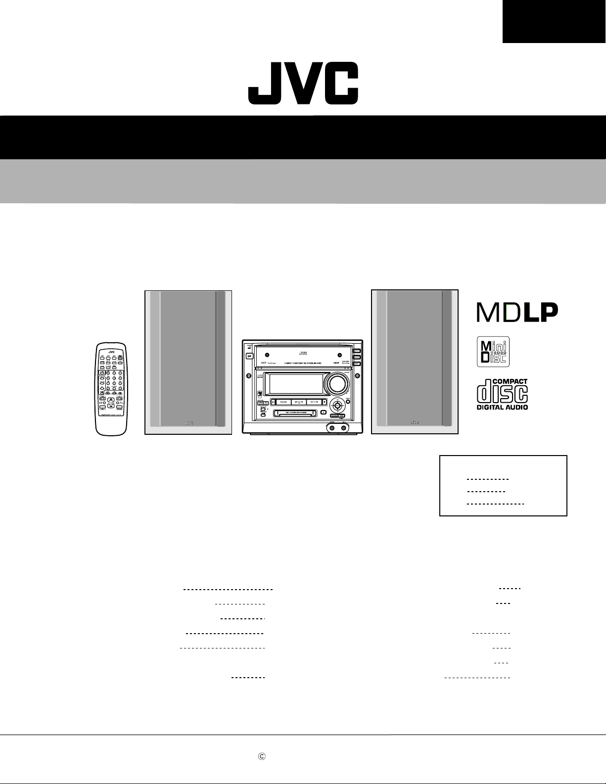
SERVICE MANUAL
COMPACT COMPONENT MD SYSTEM
MX-S6MD
MX-S6MD
Contents
Safety Precautions
Preventing static electricity
Important for laser products
Disassembly method
Adjustment method
Flow of functional operation
until TOC read (MD section)
CA-MXS6MDSP-MXS6MD SP-MXS6MD
1-2
1-3
1-4
1-5
1-31
1-37
Maintenace of laser pickup (MD)
Replacement of laser pickup (MD)
Flow of functional operation
until TOC read (CD section)
Maintenance of laser pickup (CD)
Replacement of laser pickup (CD)
Description of major ICs
US
UB
UT
Area Suffix
Singapore
Hong Kong
Taiwan
1-38
1-38
1-39
1-40
1-40
1-40~69
COPYRIGHT 2000 VICTOR COMPANY OF JAPAN, LTD.
No.20887
Nov. 2000
Page 2
MX-S6MD
1. This design of this product contains special hardware and many circuits and components specially
for safety purposes. For continued protection, no changes should be made to the original design
unless authorized in writing by the manufacturer. Replacement parts must be identical to those
used in the original circuits. Services should be performed by qualified personnel only.
2. Alterations of the design or circuitry of the product should not be made. Any design alterations of
the product should not be made. Any design alterations or additions will void the manufacturer`s
warranty and will further relieve the manufacture of responsibility for personal injury or property
damage resulting therefrom.
3. Many electrical and mechanical parts in the products have special safety-related characteristics.
These characteristics are often not evident from visual inspection nor can the protection afforded
by them necessarily be obtained by using replacement components rated for higher voltage,
wattage, etc. Replacement parts which have these special safety characteristics are identified in
the Parts List of Service Manual. Electrical components having such features are identified by
shading on the schematics and by ( ) on the Parts List in the Service Manual. The use of a
substitute replacement which does not have the same safety characteristics as the recommended
replacement parts shown in the Parts List of Service Manual may create shock, fire, or other
hazards.
4. The leads in the products are routed and dressed with ties, clamps, tubings, barriers and the
like to be separated from live parts, high temperature parts, moving parts and/or sharp edges
for the prevention of electric shock and fire hazard. When service is required, the original lead
routing and dress should be observed, and it should be confirmed that they have been returned
to normal, after re-assembling.
5. Leakage currnet check (Electrical shock hazard testing)
After re-assembling the product, always perform an isolation check on the exposed metal parts
of the product (antenna terminals, knobs, metal cabinet, screw heads, headphone jack, control
shafts, etc.) to be sure the product is safe to operate without danger of electrical shock.
Do not use a line isolation transformer during this check.
Plug the AC line cord directly into the AC outlet. Using a "Leakage Current Tester", measure
the leakage current from each exposed metal parts of the cabinet , particularly any exposed
metal part having a return path to the chassis, to a known good earth ground. Any leakage
current must not exceed 0.5mA AC (r.m.s.)
Alternate check method
Plug the AC line cord directly into the AC outlet. Use an AC voltmeter having, 1,000 ohms
per volt or more sensitivity in the following manner. Connect a 1,500 10W resistor paralleled by
a 0.15 F AC-type capacitor between an exposed
metal part and a known good earth ground.
Measure the AC voltage across the resistor with the
AC voltmeter.
AC VOLTMETER
(Having 1000
ohms/volts,
or more sensitivity)
Move the resistor connection to eachexposed metal
part, particularly any exposed metal part having a
return path to the chassis, and meausre the AC
voltage across the resistor. Now, reverse the plug in
the AC outlet and repeat each measurement. voltage
measured Any must not exceed 0.75 V AC (r.m.s.).
0.15 F AC TYPE
1500 10W
Place this
probe on
each exposed
metal part.
This corresponds to 0.5 mA AC (r.m.s.).
Good earth ground
1. This equipment has been designed and manufactured to meet international safety standards.
2. It is the legal responsibility of the repairer to ensure that these safety standards are maintained.
3. Repairs must be made in accordance with the relevant safety standards.
4. It is essential that safety critical components are replaced by approved parts.
5. If mains voltage selector is provided, check setting for local voltage.
!
Burrs formed during molding may be left over on some parts of the chassis. Therefore,
pay attention to such burrs in the case of preforming repair of this system.
1-2
Page 3
MX-S6MD
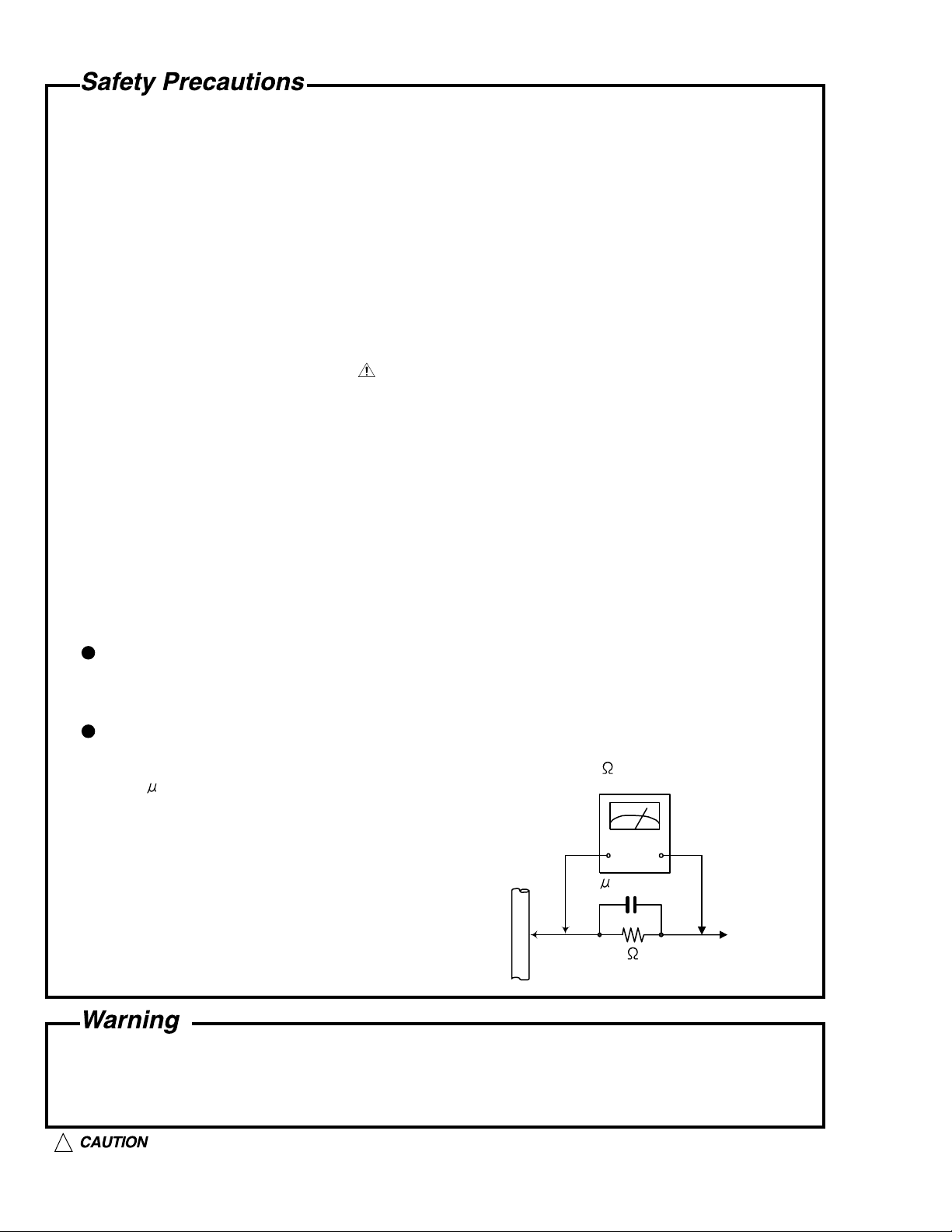
Preventing static electricity
Electrostatic discharge (ESD), which occurs when static electricity stored in the body, fabric, etc. is discharged,
can destroy the laser diode in the traverse unit (optical pickup). Take care to prevent this when performing repairs.
1.1. Grounding to prevent damage by static electricity
Static electricity in the work area can destroy the optical pickup (laser diode) in devices such as CD/MD players.
Be careful to use proper grounding in the area where repairs are being performed.
1.1.1. Ground the workbench
1. Ground the workbench by laying conductive material (such as a conductive sheet) or an iron plate over
it before placing the traverse unit (optical pickup) on it.
1.1.2. Ground yourself
1. Use an anti-static wrist strap to release any static electricity built up in your body.
(caption)
Anti-static wrist strap
Conductive material
(conductive sheet) or iron plate
1.1.3. Handling the optical pickup
1. In order to maintain quality during transport and before installation, both sides of the laser diode on the
replacement optical pickup are shorted. After replacement, return the shorted parts to their original condition.
(Refer to the text.)
2. Do not use a tester to check the condition of the laser diode in the optical pickup. The tester's internal power
source can easily destroy the laser diode.
1.2. Handling the traverse unit (optical pickup)
1. Do not subject the traverse unit (optical pickup) to strong shocks, as it is a sensitive, complex unit.
2. Cut off the shorted part of the flexible cable using nippers, etc. after replacing the optical pickup. For specific
details, refer to the replacement procedure in the text. Remove the anti-static pin when replacing the traverse
unit. Be careful not to take too long a time when attaching it to the connector.
3. Handle the flexible cable carefully as it may break when subjected to strong force.
4. It is not possible to adjust the semi-fixed resistor that adjusts the laser power. Do not turn it
Main board
CN451
Flexible board
MD pickup
CN321
Soldering part
CD pickup
Pickup Soldering part
1-3
Page 4
MX-S6MD
Important for laser products
1.CLASS 1 LASER PRODUCT
2.DANGER : Invisible laser radiation when open and inter
lock failed or defeated. Avoid direct exposure to beam.
3.CAUTION : There are no serviceable parts inside the
Laser Unit. Do not disassemble the Laser Unit. Replace
the complete Laser Unit if it malfunctions.
4.CAUTION : The compact disc player uses invisible
laserradiation and is equipped with safety switches
whichprevent emission of radiation when the drawer is
open and the safety interlocks have failed or are de
feated. It is dangerous to defeat the safety switches.
VARNING : Osynlig laserstrålning är denna del är öppnad
och spårren är urkopplad. Betrakta ej strålen.
VARO : Avattaessa ja suojalukitus ohitettaessa olet
alttiina näkymättömälle lasersäteilylle.Älä katso
säteeseen.
5.CAUTION : If safety switches malfunction, the laser is able
to function.
6.CAUTION : Use of controls, adjustments or performance of
procedures other than those specified herein may result in
hazardous radiation exposure.
CAUTION
!
Please use enough caution not to
see the beam directly or touch it
in case of an adjustment or operation
check.
ADVARSEL : Usynlig laserstråling ved åbning , når
sikkerhedsafbrydere er ude af funktion. Undgå
udsættelse for stråling.
ADVARSEL : Usynlig laserstråling ved åpning,når
sikkerhetsbryteren er avslott. unngå utsettelse
for stråling.
REPRODUCTION AND POSITION OF LABEL
WARNING LABEL
CLASS 1
LASER PRODUCT
DANGER : Invisibie laser radiation
when open and interlock or
defeated.
AVOID DIRECT EXPOSURE TO
BEAM (e)
VARNING : Osynlig laserstrålning är
denna del är öppnad och spårren är
urkopplad. Betrakta ej strålen. (s)
VARO : Avattaessa ja suojalukitus
ohitettaessa olet alttiina
näkymättömälle lasersäteilylle.Älä
katso säteeseen. (d)
ADVARSEL :Usynlig laserstråling
ved åbning , når
sikkerhedsafbrydere er ude af
funktion. Undgå udsættelse for
stråling. (f)
1-4
Page 5
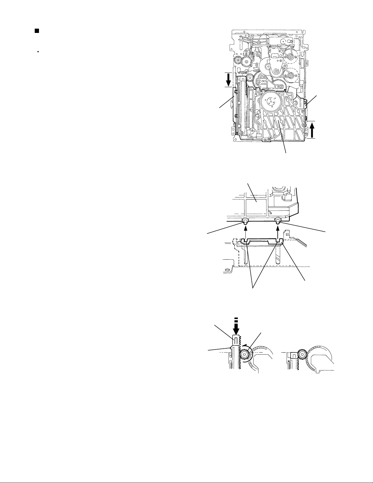
Disassembly method
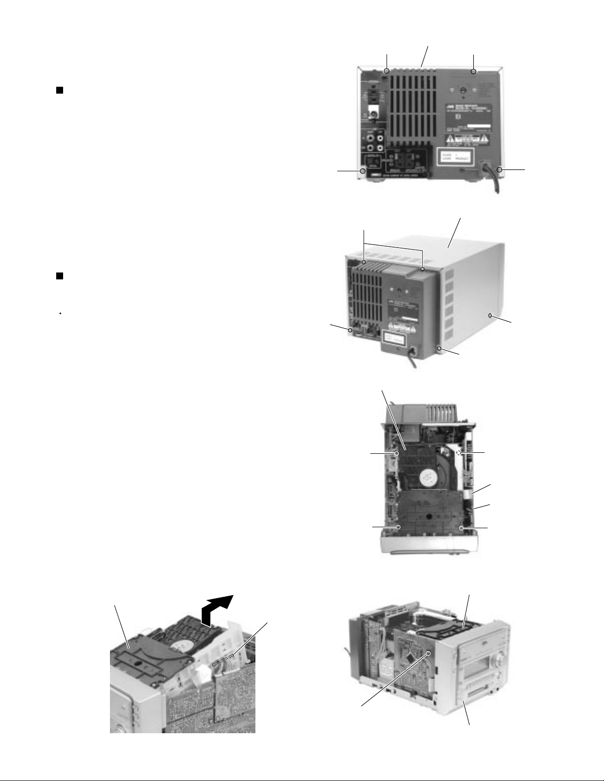
<Main body>
Removing the top cover
(See Fig. 1 and 2)
1.
Remove the four screws A on the back of the body.
2.
Remove the two screws B on both sides of the body.
A
MX-S6MD
Top cover
A
3.
Lift up the rear part of the top cover while pulling
both sides, then remove the top cover.
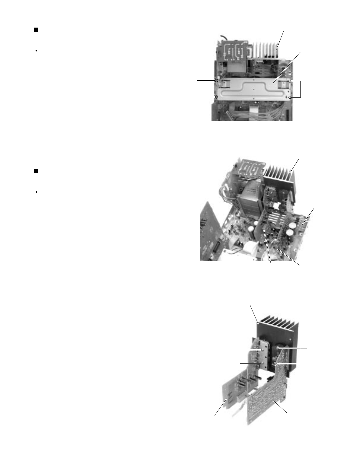
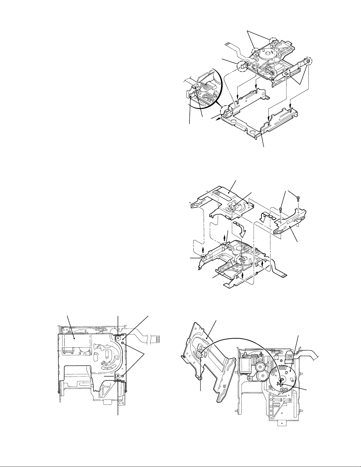
Removing the CD changer mechanism
assembly (See Fig.3 to 5)
Prior to performing the following procedure, remove
the top cover.
1.
Disconnect the card wire from connector CN661 on
the input board.
2.
Remove the four screws C on the upper side of the
body.
3.
Remove the screw D on the left side of the body.
4.
Release the wires from the clamp on the right side of
the CD changer mechanism assembly. Lift up the
rear part of the CD changer mechanism assembly
and pull out it from the front assembly.
A
Fig.1
A
A
Fig.2
CD changer mechanism assembly
C
Top cover
A
C
CN661
Bx
A
2
CD changer mechanism assembly
Clamp
D
C
Input board
C
Fig.3
CD changer mechanism assembly
Front panel assembly
Fig.4Fig.5
1-5
Page 6
MX-S6MD
Removing the font panel assembly
(See Fig.6 to 8)
Prior to performing the following procedure, remove
the top cover.
1.
Disconnect the wire from connector CN603 on the
input board and the card wire from CN801 on the
microcomputer board.
2.
Remove the two screws E on the bottom of the body.
3.
Release the joint a on the bottom and the two joints
b and c on the lower sides of the body using a
screwdriver. Detach the front panel assembly toward
the front.
Front panel assembly
Front panel assembly
E
Front panel assembly
Fig.6
CN603
Joint
a
E
Microcomputer board
Fig.8
CN801
Joint c
Removing the display board (See Fig.9)
Prior to performing the following procedure, remove
the top cover and the front panel assembly.
1.
Remove the nine screws F attaching the display
board to the front panel assembly.
2.
Disconnect connector CN791 on the display board
from the control board on the front panel assembly.
Removing the control board / the key
board (See Fig.10)
Prior to performing the following procedure, remove
the top cover, the front panel assembly and the
display board.
F
CN791
Joint b
Fig.7
F
F
Front panel assembly
Fig.9
H
Input board
Front panel assembly
F
Display board
Key board
1.
Remove the five screws G and the four screws H
attaching the control board and the key board.
REFERANCE
1-6
:
When removing the control board and
the key board respectively, unsolder
each board.
G
G
Soldering
Fig.10
G
Control board
H
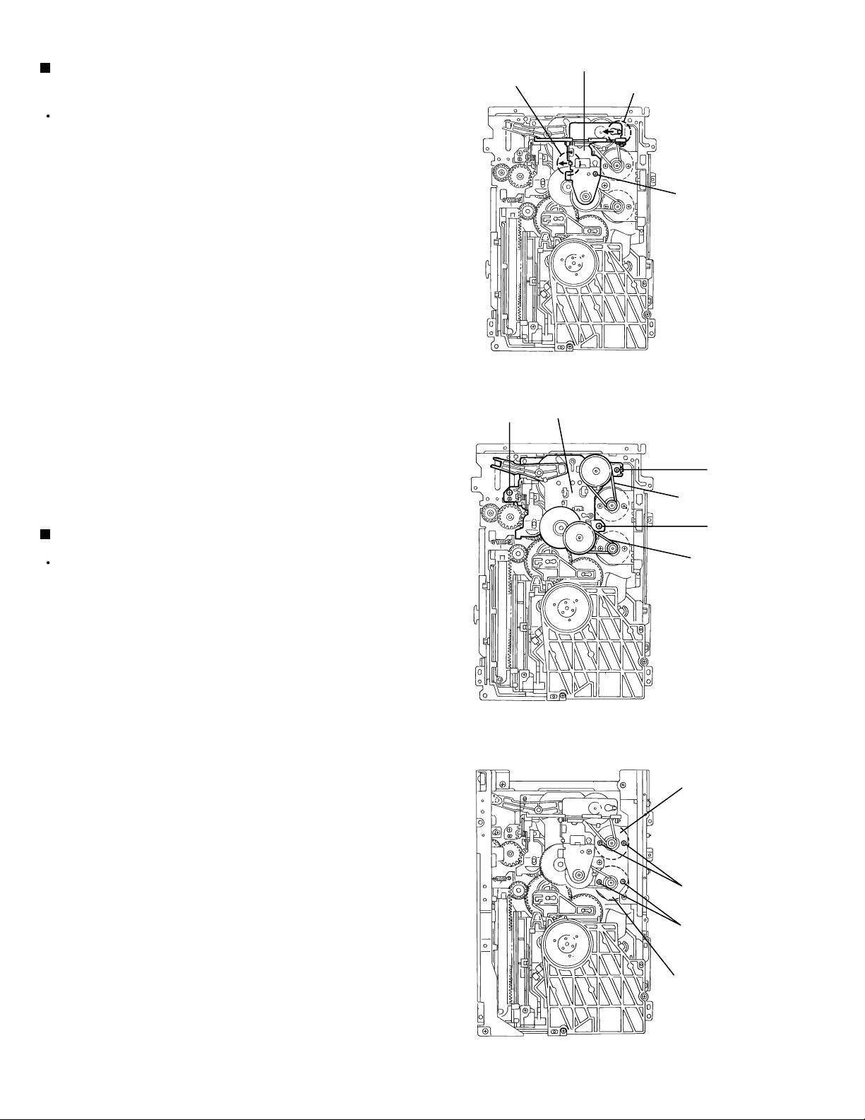
Page 7
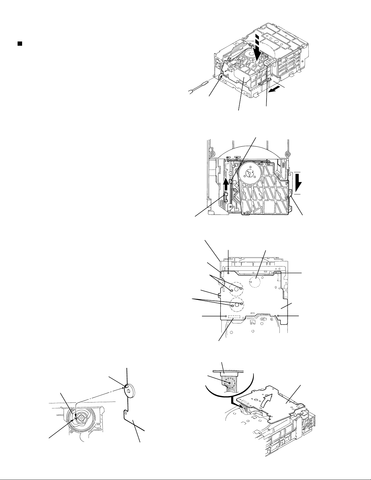
Removing the MD changer mechanism
(See Fig.11 to 13 )
Prior to performing the following procedure, remove
the top cover and the CD changer mechanism
assembly.
1.
Disconnect the card wire from connectors CN511 on
the main board.
2.
Remove the four screws I on both sides of the body.
3.
Pull out the MD changer mechanism assembly from
behind upward while releasing the four joints d using
a screwdriver.
MX-S6MD
MD changer
mechanism assembly
I
Fig.11
Removing the microcomputer board
(See Fig.14)
Prior to performing the following procedure, remove
the top cover.
1.
Disconnect the card wire from connector CN801 on
the microcomputer board.
2.
Remove the screw D attaching the microcomputer
board.
3.
Disconnect the lower connector CN391, CN392 and
CN393 from the main board by pulling them.
Joints
I
Fig.12
d
MD changer mechanism assembly
Fig.13
MD changer
mechanism assembly
CN511
Joints
Microcomputer board
d
Fig.14
D
CN801
CN393
CN392
CN391
1-7
Page 8
MX-S6MD
Removing the tuner board
(See Fig.15 and 16)
Prior to performing the following procedure, remove
the top cover.
1.
Disconnect the wire from connector CN
CN112 on the tuner board.
2.
Remove the screw J on the side of the body
Remove the two screws K on the back of the rear
3.
panel.
REFERANCE
:
To facilitate the procedure, remove the
rear panel in advance.
111 and
.
Remove the rear cover / the rear panel
(See Fig.15 to 17)
Prior to performing the procedure, remove the top
cover.
1.
Remove the two screws L and the two screws L'
attaching the rear cover to the body.
2.
Remove the two screws K, M, N, O, and the screw P
and Q respectively.
3.
Release the joint e on the lower left side of the rear
panel.
J
K
CN112
Tuner board
Rear panel
Q
CN111
Fig.15
e
Joint
Fig.16
Rear panel
K
L
L'
Rear cover
L
O
Removing the Input board
Prior to performing the procedure, remove the top
cover, the rear cover, the rear panel and the tuner
board.
1.
Disconnect the card wire from connector CN661 and
the wire from CN603 on the input board.
2.
Remove the two screws R attaching the bracket and
remove the bracket in the direction of the arrow.
3.
Disconnect the lower connector CN602, CN913 and
CN922 from the main board. Disconnect the wire
from CN691 on the input board.
1-8
(See Fig.18)
M
Input board
CN691
CN602
CN603
CN913
N
CN661
CN922
P
Fig.17
R
Fig.18
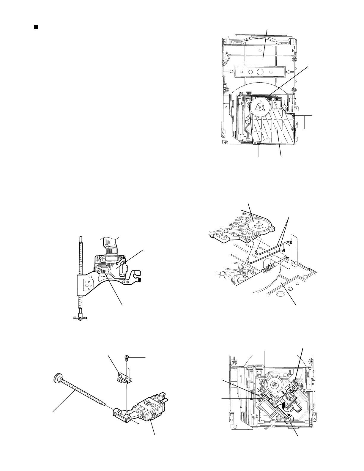
Page 9
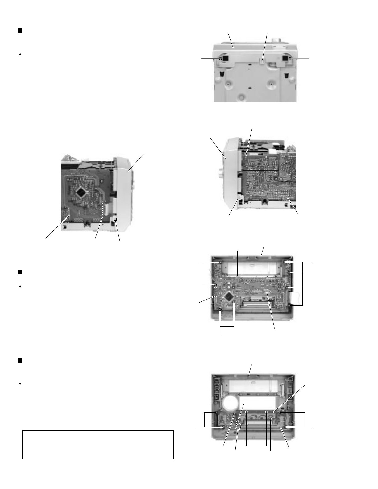
MX-S6MD
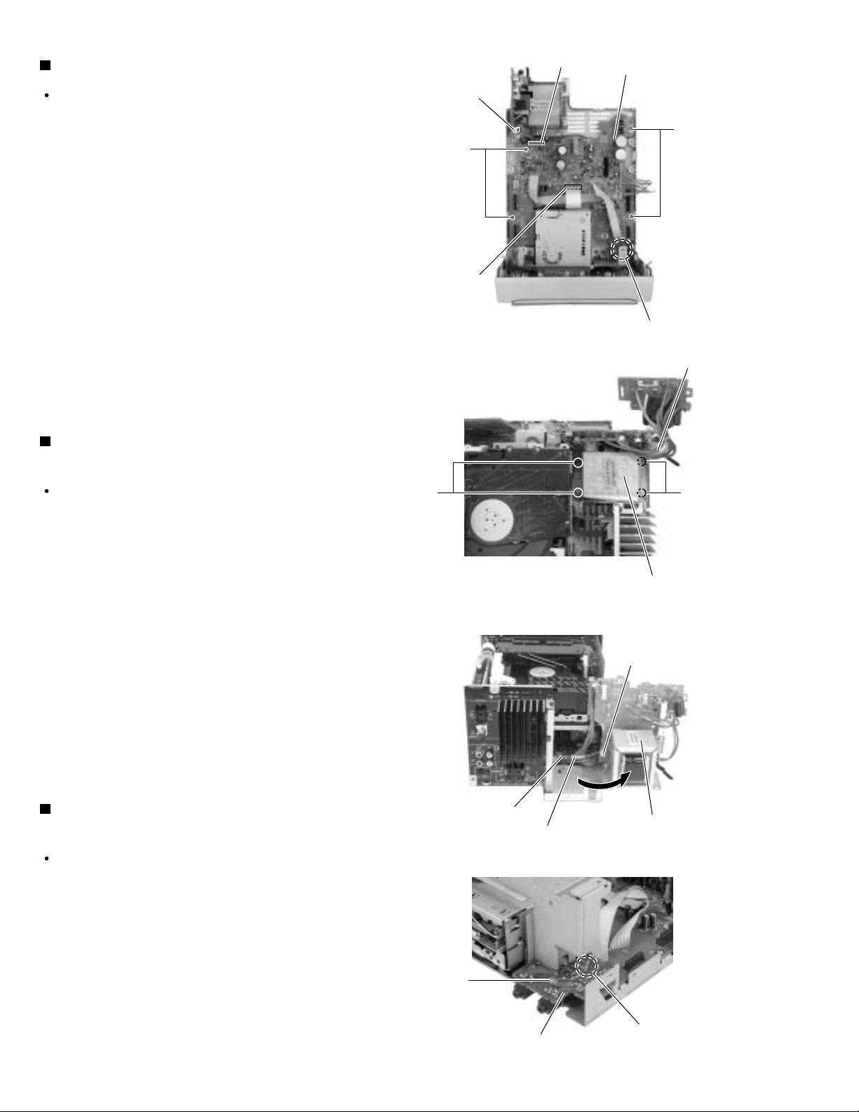
Removing the heat sink assembly
(See Fig.19 and 20)
Prior to performing the procedure, remove the top
cover, the CD changer mechanism assembly, the
rear cover, the rear panel, the tuner board and the
input board.
1.
Remove the four screws S attaching the bracket.
2.
Disconnect connector CN924 and CN394 from the
main board.
Removing the regulator board / the
amplifier board (See Fig.21)
Prior to performing the procedure, remove the top
cover, the CD changer mechanism assembly, the
rear cover, the rear panel, the tuner board, the input
board and the heat sink assembly.
S
Heat sink assembly
Bracket
S
Fig.19
Heat sink assembly
Main board
1.
Remove the two screws T or U attaching the
regulator board and the amplifier board to the heat
sink.
T
Fig.20
Heat sink
CN924
CN394
U
Regulator board
Amplifier board
Fig.21
1-9
Page 10
MX-S6MD
Removing the Main board (See Fig.22)
Prior to performing the procedure, remove the top
cover, the CD changer mechanism assembly, the
rear cover, the rear panel, the tuner board, the input
board and the heat sink assembly.
1.
Disconnect the wire from connector CN911 on the
main board and CN991 on the power transformer
assembly.
2.
Disconnect the card wire from connector CN511 on
the main board.
3.
Remove the four screws V attaching the main
board.
4.
If necessary, unsolder the wire on the headphone
board.
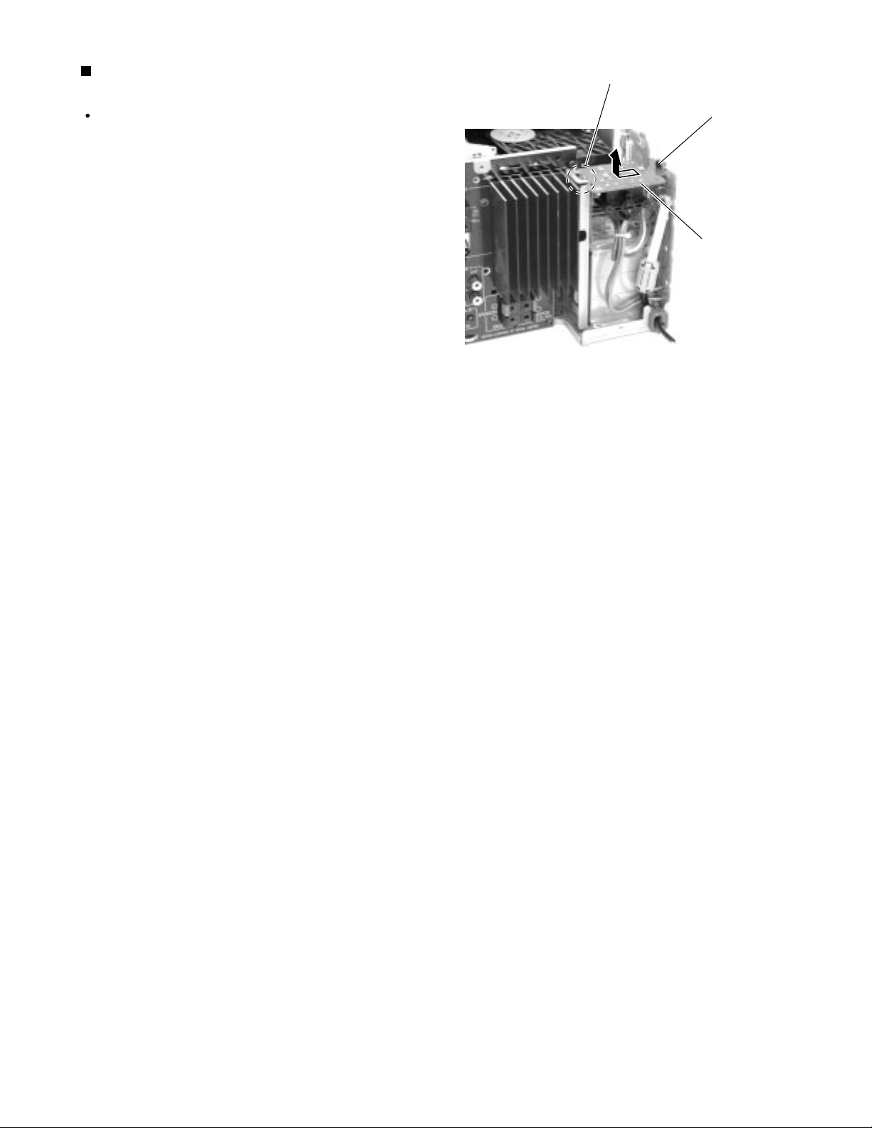
Removing the power transformer
assembly (See Fig.23 and 24)
CN991
V
CN511
CN911
Fig.22
Main board
V
Soldering
Power cord stopper
Prior to performing the following procedure, remove
the top cover, the rear cover, the voltage selector.
1.
Remove the four screws W attaching the power
transformer assembly.
2.
Pull out the power cord stopper from the body
upward. Turn the power transformer assembly while
lifting it as shown in the figure.
3.
Disconnect the wire from connector CN911 on the
main board and CN991 on the power transformer
board. Remove the power transformer assembly
from the body.
Removing the headphone board
(See Fig.25)
Prior to performing the procedure, remove the top
cover, the CD changer mechanism assembly, the
front panel assembly, the rear cover, the rear panel,
the tuner board and the input board.
W
Main board
W
Power transformer assembly
Fig.23
CN991
Power transformer assembly
CN911
Fig.24
1.
Remove the screw X attaching the headphone
board.
If necessary, unsolder the wire on the headphone
board.
1-10
X
Headphone board
Soldering
Fig.25
Page 11
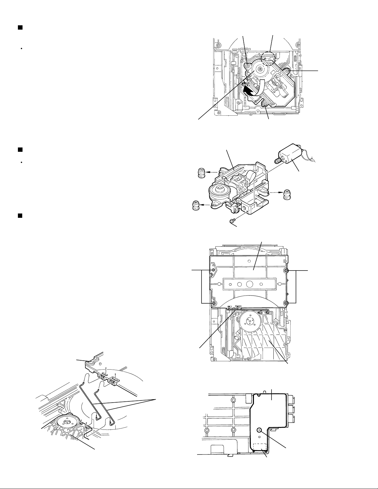
MX-S6MD
Removing the voltage selector
(See Fig.26)
Prior to performing the following procedure, remove
the top cover and the rear cover.
1.
Remove the plastic rivet retaining the voltage
selector.
2.
Disengage the joint f to release the voltage selector
from the transformer bracket. If necessary, unsolder
each wire.
Joint
Fig.26
f
Plastic rivet
Voltage selector
1-11
Page 12
MX-S6MD
<MD section>
AA
(Bottom)
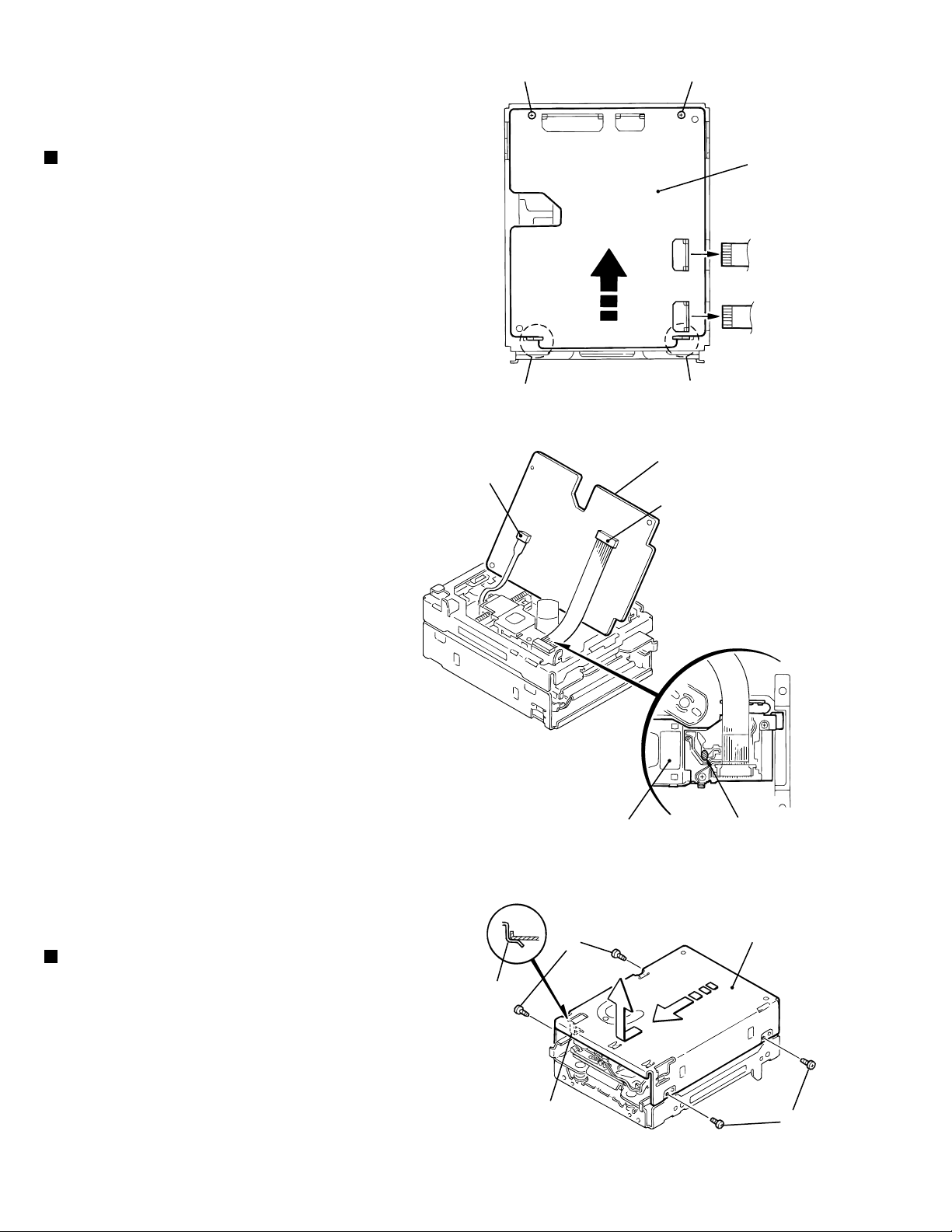
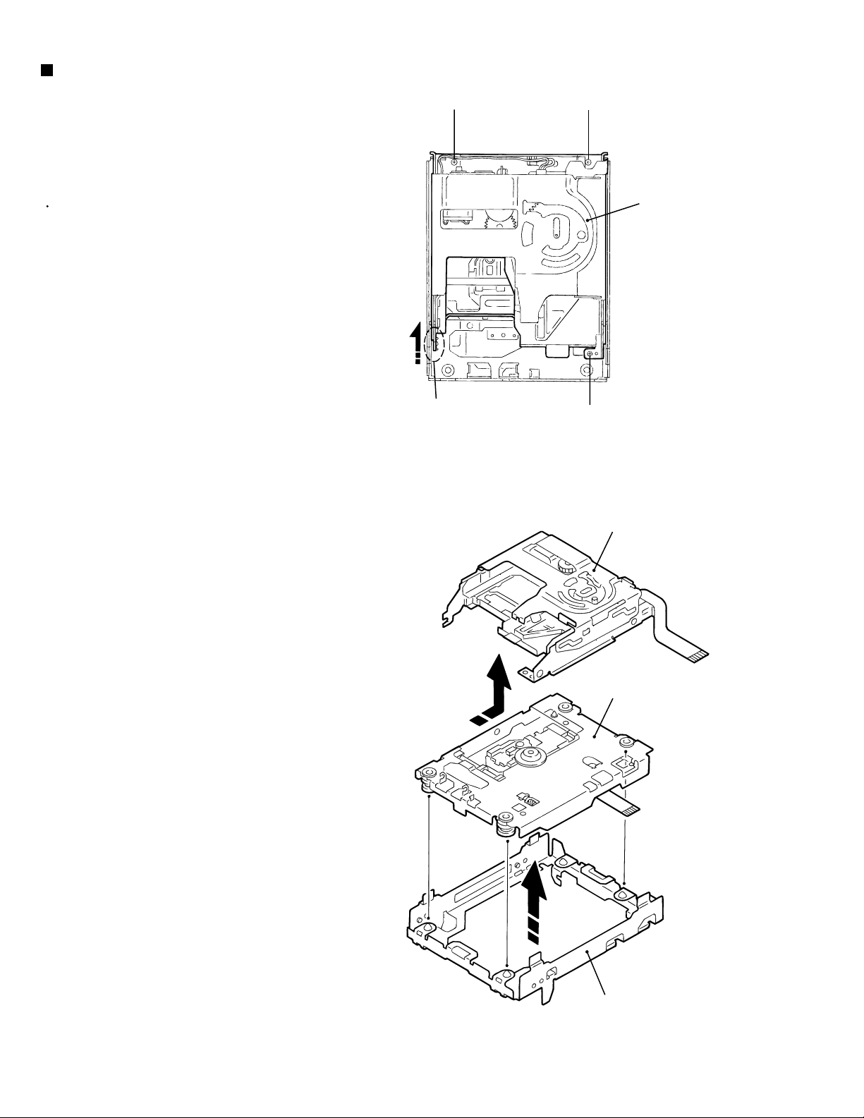
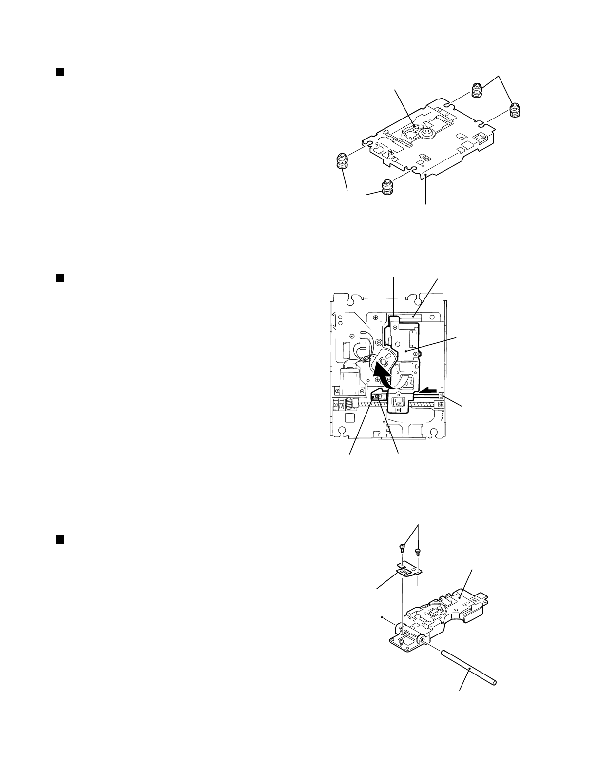
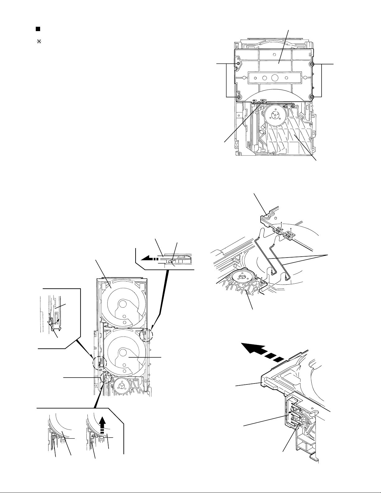
Removing the main board
(See Fig.1 and 2)
1.
Turn over the body and disconnect the card wire
from connector CN408 and the flexible wire from
CN407 on the main board.
2.
Remove the two screws A attaching the main board.
Slide the main board in the direction of the arrow to
release the two joints a with the single flame.
3.
Solder part b on the pickup in the body. Disconnect
the flexible harness from connector CN321 and
CN451 on the underside of the main board. Then
remove the main board.
Main board
CN408
CN407
Joint b Joint b
Fig.1
Main board
CN451
CN321
Removing the mechanism cover
(See Fig.3)
1.
Remove the four screws B on both sides of the
body.
2.
Move the mechanism cover toward the front to
disengage the front hook of the mechanism cover
from the internal loading assembly (Joint c). Then
remove the mechanism cover upward.
1-12
Fook
Joint c
Joint c
B
Pickup
Fig.2
Fig.3
Solder part b
Mechanism cover
B
Page 13
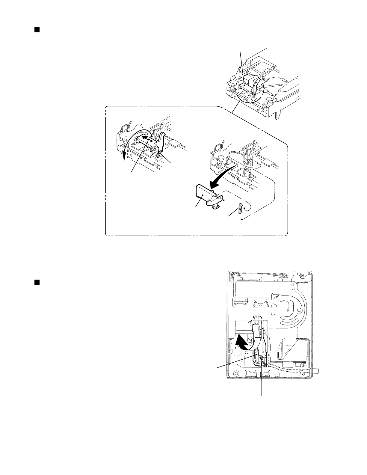
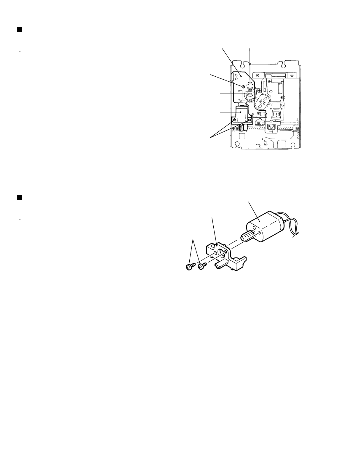
Removing the head lifter (See Fig.4 to 6)
1.
Move the head lifter on top of the body in the
direction of the arrow and turn around.
2.
Detach the spring from the hook of the body.
Remove the head lifter with the spring.
3.
If necessary, remove the spring from the head lifter.
Head lifter
Fig.5
MX-S6MD
Head lifter
Fig.4
Spring
Removing the head assembly (See Fig.7)
1.
Remove the screw C on the upper side of the body.
Remove the head assembly while pulling the flexible
harness from the body.
Head lifter
Spring
Fig.6
Head assembly
Fig.7
C
1-13
Page 14
MX-S6MD
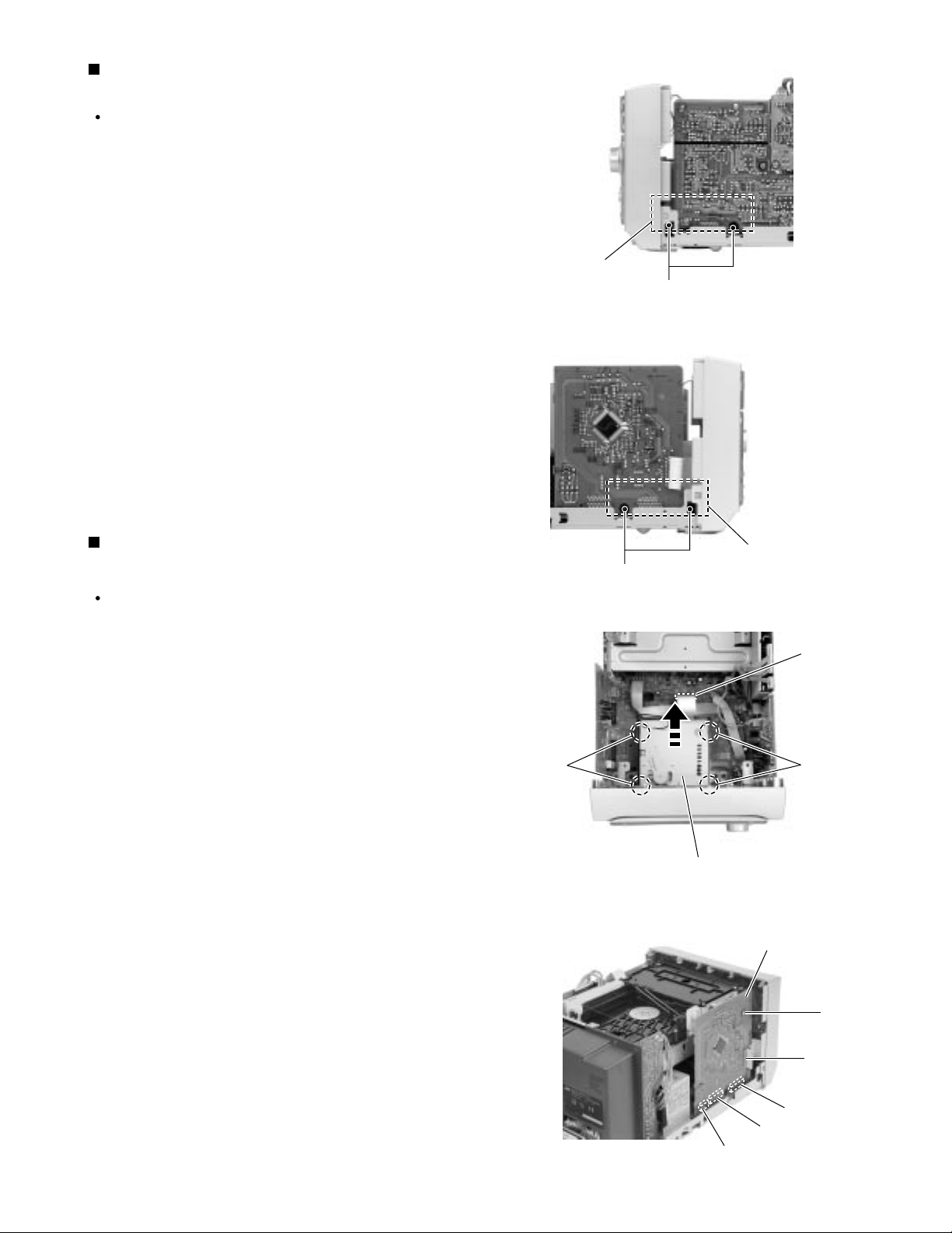
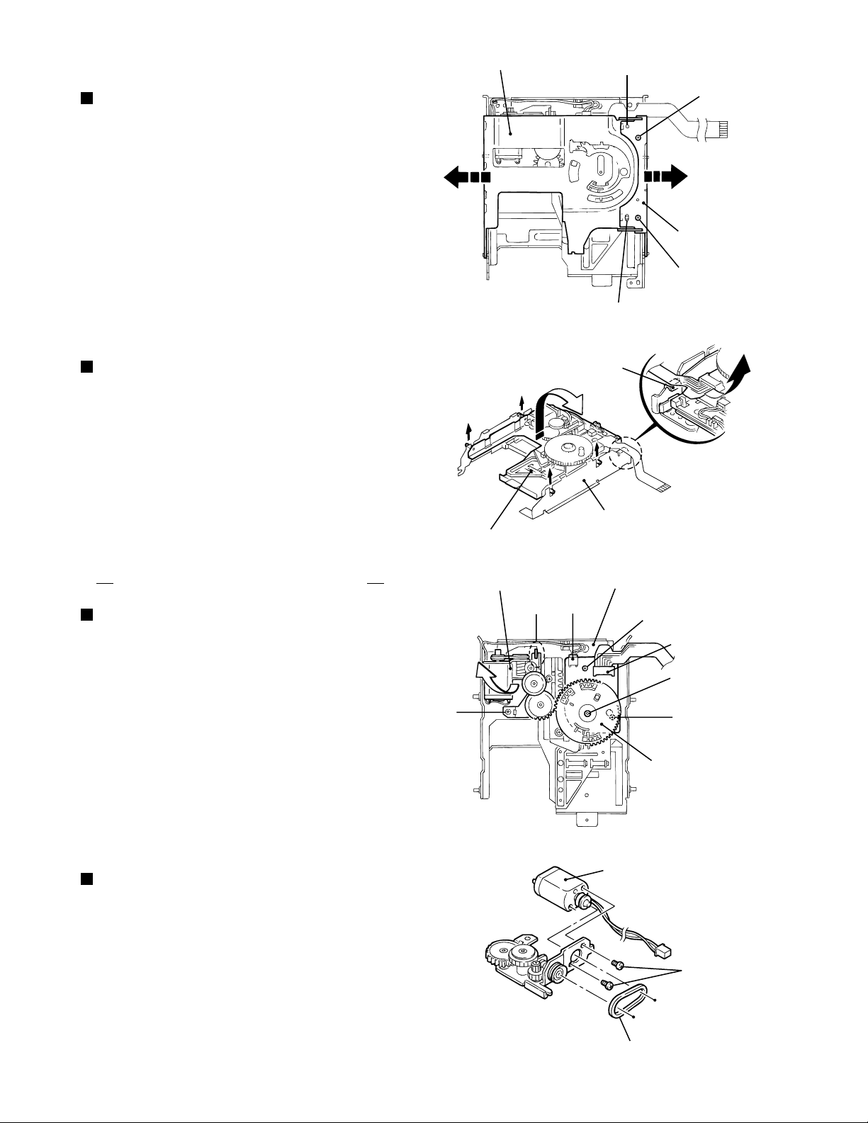
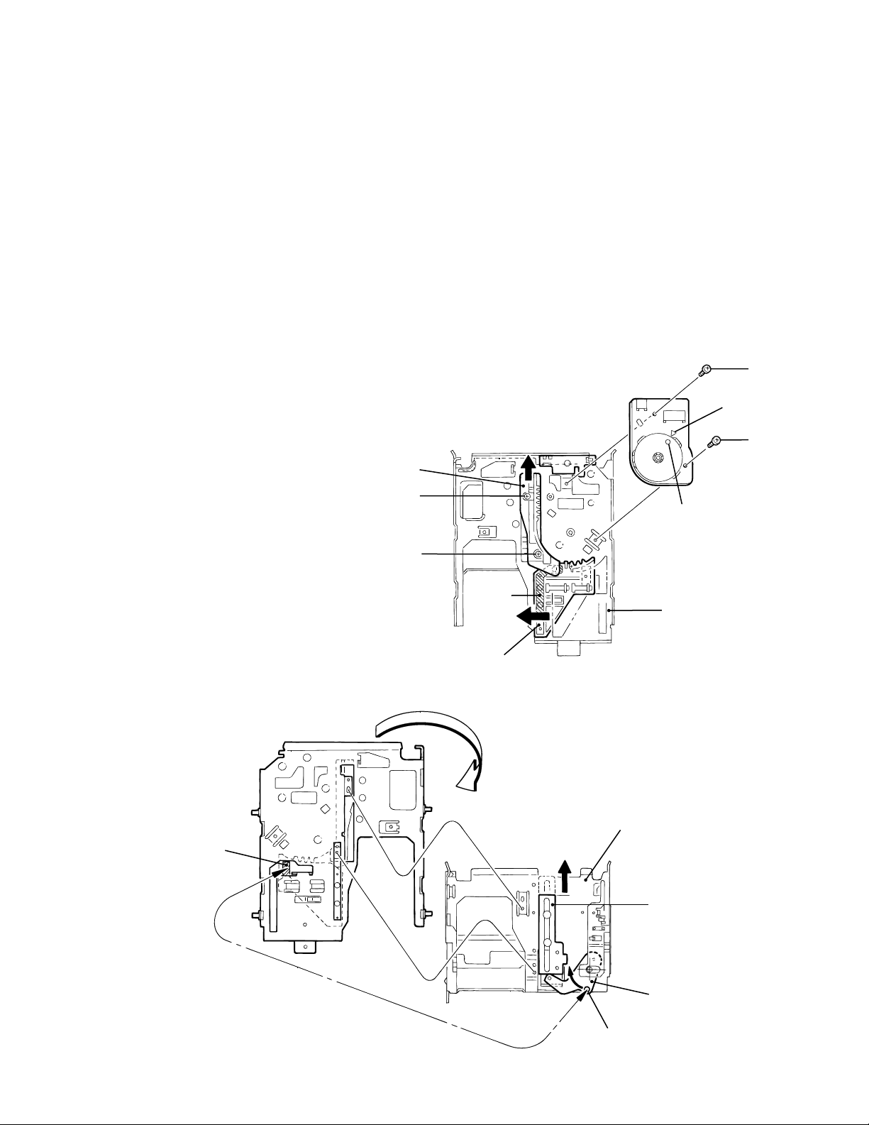
Removing the Loading assembly
Ref:
The loading assembly, the traverse mechanism
assembly and the single flame will be
removable after removing the loading assembly
from the body.
(See Fig.8 and 9)
D
D
Prior to performing the following procedure, remove
the main board, the mechanism cover, the head lifter
and the head assembly.
1.
Remove the three screws D on the upper side of the
body.
2.
Move the loading assembly forward to disengage it
from the traverse mechanism assembly (Joint d).
Then remove it upward.
3.
Remove the traverse mechanism assembly from the
single flame.
Joint d
Loading assembly
D
Fig.8
Loading assembly
1-14
Traverse mechanism
assembly
Single flame
Fig.9
Page 15
MX-S6MD
<Loading assembly>
Removing the slide base (L) / (R)
(See Fig.10)
1.
Remove the two screws E on the upper side of the
loading assembly.
2.
Remove the slide base (L) outward. (Release it from
the joint bosses E.)
3.
Remove the slide base (R) outward.
Removing the loading mechanism
assembly (See Fig.11)
1.
Detach the loading mechanism assembly upward to
release the four pins on both sides from the loading
motor, paying attention to the part e of the loading
mechanism base.
Slide base (R)
E'
E
Slide base (L)
E
E'
Fig.10
Part e
Loading mechanism assembly
Removing the loading motor
(See Fig.12 and 13)
1.
Disconnect the harnesses from the wire holder and
from connector CN612 on the cam switch board.
2.
Remove the screw F attaching the loading motor
and release the joint f.
3.
Remove the belt from the loading motor assembly.
4.
Remove the two screws G attaching the loading
motor.
Removing the cam gear and the cam
switch board (See Fig.12)
Loading mechanism
assembly
Loading motor assembly
Joint f
CN612
F
Loading mechanism base
Fig.11
Wire holder
H
Cam switch board
Slit washer
H
Cam gear
Fig.12
Loading motor
1.
Remove the slit washer attaching the cam gear and
pull out the cam gear.
2.
Disconnect the harness from the wire holder and
from connector CN612 on the cam switch board.
3.
Remove the two screws H and the clamp. Remove
the cam switch board.
G
Belt
Fig.13
1-15
Page 16
MX-S6MD
Removing the cartridge holder assembly
(See Fig.14 and 15)
1.
Remove the two screws I on the upper side of the
loading assembly.
I
I
Removing the slide bar and the eject bar
(See Fig.14 and 15)
Prior to performing the following procedure, remove
the cartridge holder assembly.
Slide bar
Cartridge holder assembly
Eject bar
Eject bar
Part g
Fig.14
I
1.
Remove the slide bar upward.
2.
Move the eject bar outward until it stops as shown in
Fig.14. Push the convex part g on the bottom of the
body and remove the eject bar from the chassis.
Slide bar
k
Eject bar
UD base
1-16
Cartridge holder assembly
Fig.15
Page 17
<Traverse mechanism assembly>
MX-S6MD
Removing the Insulators (See Fig.16)
1.
Disengage the four insulators from the notches of the
traverse mechanism chassis.
Removing the pickup unit (See Fig.17)
1.
Turn over the traverse mechanism assembly and
remove the screw J attaching the shaft holder (F).
2.
Move the shaft inward and remove it from the shaft
holder (R).
Pickup unit
Insulators
Traverse machanism chassis
Fig.16
Joint h
Pickup guide
Pickup unit
Insulators
3.
Detach the shaft side of the pickup unit upward and
release the joint h with the pickup guide. Then
remove the pickup unit with the shaft.
Removing the pickup (See Fig.18)
1.
Draw out the shaft from the pickup.
2.
Remove the two screws K attaching the rack spring.
Shaft holder (F)
Rack spring
Shaft holder (R)
J
Fig.17
K
Pickup
Fig.18
Shaft
1-17
Page 18
MX-S6MD
Removing the feed motor assembly
(See Fig.19-1, 19-2)
It is not necessary to remove the pickup unit.
1.
For the white and black harnesses extending from
the feed motor assembly, unsolder the soldering i on
the traverse mechanism board.
Traberse mechanism board Soldering j
M
2.
Remove the two screws L attaching the feed motor
assembly.
3.
Remove the two screws N attaching the feed motor
bracket.
Removing the traverse mechanism
board (See Fig.19-1)
Prior to performing procedure, remove the feed
motor assembly.
1.
For the red and black harnesses extending from the
spindle motor, unsolder the soldering j on the
traverse mechanism board.
Soldering i
Feed motor assembly
L
Fig.19-1
Feed motor
Feed motor bracket
N
2.
Remove the screw M attaching the traverse
mechanism board.
Fig.19-2
1-18
Page 19
<Reattaching the loading assembly>
1.
Reattach the eject bar to the UD base.
(Fig.15 and 20)
2.
Reattach the slide bar to the loading mechanism
chassis while fitting the boss marked k to the eject
bar slot. (Fig.20)
3.
Slide the slide bar and the eject bar in the direction
of the arrow in Fig.20 and reattach the cartridge
holder assembly using the two screws I.
(Fig.20 and 21)
MX-S6MD
ATTENTION:
Make sure the pin of the eject lever
marked l is fitted to the slot of the eject
bar marked m at the bottom of the
loading mechanism chassis after
moving the eject lever and the loading
slider of the cartridge holder assembly
in the direction of the arrow.
(Refer to Fig.21)
Slide bar
I
I
Cam switch board
H
Point marked
H
Cam switch boss
Ditch
UD base
Eject bar
Fig.20
Ditch m
UD base (Bottom)
Cartridge holder assembly
Loading slider
Eject lever
l
Fig.21
1-19
Page 20
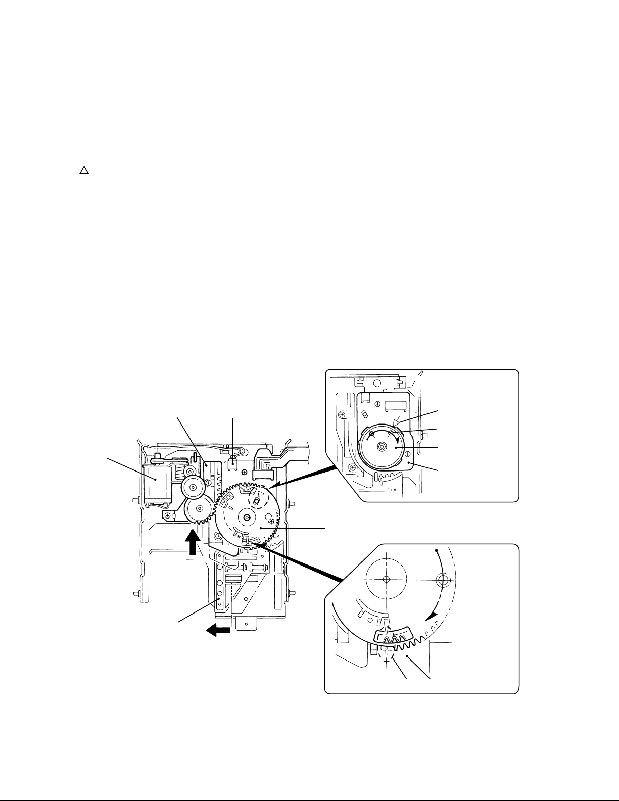
MX-S6MD
4.
Reattach the wire holder to the UD base while
engaging the UD base hook marked u to the wire
holder slot marked t (At the same time, the boss on
the reverse side of the wire holder is fitted to the UD
base round hole).
5.
Reattach the cam switch board using the two screws
H. (Fig.22)
6.
Turn the cam switch to bring the boss to the point
marked on the cam switch board. Reattach the
cam gear using a slit washer while fitting the cam
gear slot to the cam switch boss. (Fig.22)
ATTENTION:
When reattaching the cam gear, the
cam switch boss should be fitted to the
cam gear slot, and the triangle mark of
the cam gear should be aligned to the
hole of the eject bar as shown in
Fig.22.
7.
Reattach the loading motor assembly, using the
screw F. Connect the harness extending from the
loading motor to connector CN612 on the switch
board and fix it with the wire holder. (Fig.22)
Slide bar CN612
Loading motor assembly
Point marked
Boss
Cam switch
Cam switch board
1-20
F
Eject lever
Fig.22
Cam gear
n
Cam gear
(Triangle mark)
Eject lever
Page 21
MX-S6MD
8.
Reattach the UD base while engaging the four pins
on both sides of the UD base to the notches of the
loading mechanism base and placing the edge
(marked e’) of the cartridge holder assembly under
the hook e of the loading mechanism base. (Fig.23)
9.
Reattach the slide base (R) while fitting the two pins
on another side of the UD base to the slots of the
slide base (R). (Fig.24)
ATTENTION:
10.
Reattach the slide base (L) on the slide base (R)
while fitting the two pins on another side of the UD
base to the slots of the slide base (L) (Fig.25). Make
sure the two slots of the slide base (L) are fitted to
the two bosses marked E’ and tighten the two
screws E. (Fig.26)
Ref:
To expedite the work, bring up the UD base
slightly when fitting each pin to the appropriate
notch.
Fit the part v of the slide base (R) to
the part w on the inward side of the
cam gear rib. (Fig.25)
Hook e
Hook e'
Hook e'
Pin
Loading mechanism base
Fig.23
Slide base (R)
Part v
Pin
E
E'
Pin
Slide base (L)
Pin
Part w
Fig.24
Slide base (L)Slide base (R)
Slide base (R)
Cam gear
E
Part v
Part w
E'
Fig.25Fig.26
1-21
Page 22
MX-S6MD
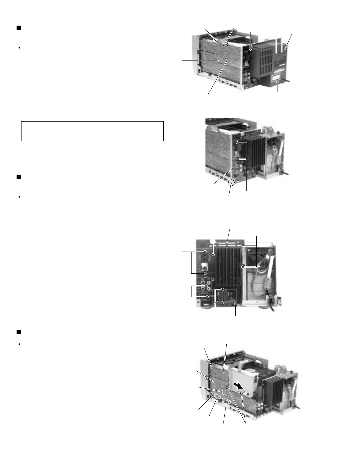
<CD mechanism section>
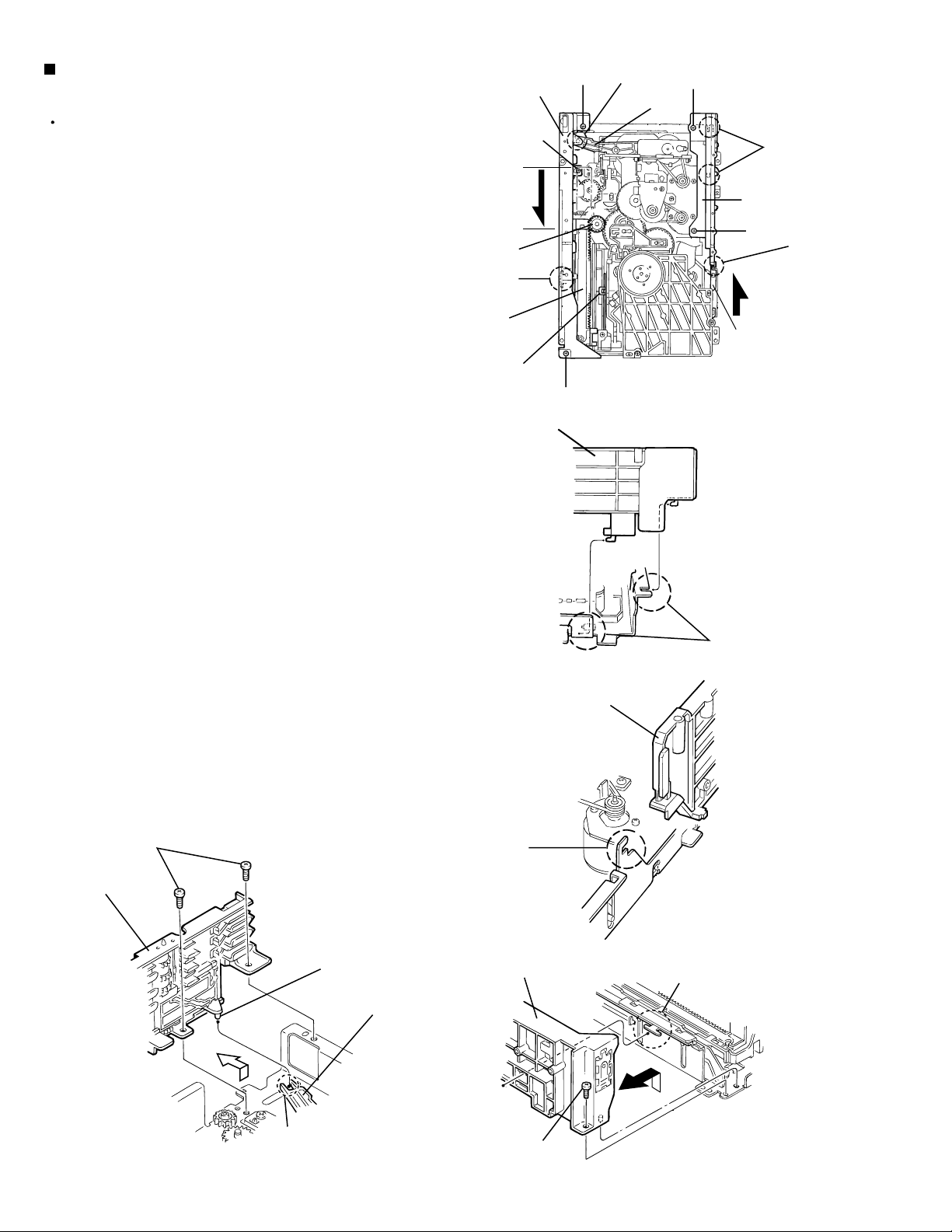
Removing the servo control board
(See Fig.1 to 4)
ATTENTION:
1.
Insert a screwdriver into the sub chassis slot on the
back of the body and push the slider (R) toward the
front.
2.
From the top of the body, slide the hook and the
slider (R) forward until they stop.
3.
From the right side of the body, slide the slide cam
(L) backward until it stops. The sub chassis unit will
move to the lowest position.
4.
From the bottom of the body, unsolder each soldered
part a and b of the motors on the servo control
board.
5.
Remove the five screws A attaching the servo
control board.
6.
Disconnect connector CN610 on the servo control
board from the tray select switch board to suspend
the servo control board tentatively. Solder the part c
of the flexible wire connected to connector CN601 on
the underside of the servo control board.
Make sure the sub chassis unit is
locating at the lowest position. If
not,perform the following procedure
from 1 to 3.
Slot
Sub chassis unit
Hook
Tray select switch board
A
CN610
Slide cam (L)
Fig.1
Slider (R)
Slide cam (L)
Fig.2
Cam switch
7.
Disconnect the flexible wire from connector CN601
and remove the servo control board from the body.
ATTENTION:
ATTENTION:
Control cam
Slot p
In case of disconnecting the flexible
wire without soldering, the CD pick up
may be damaged.
When reassembling, make sure the
cam switch boss of the servo control
board is fitted to the slot p of the
control cam on the bottom of the body
(Refer to Fig.3-1).
Cam switch boss
Gear base unit
Main board
Solder part a
A
Solder
part b
A
Solder part c
CN601
CN601
A
Servo
control board
A
Fig.3-1
Servo control board
Fig.4Fig.3-2
1-22
Page 23
MX-S6MD
Removing the tray unit (See Fig.5 to 8)
The tray unit can be removed despite the position of
the sub chassis unit, but the lowest position is
recommended to expedite the work.
1.
Remove the four screws B attaching the top cover
on the top of the body.
2.
Remove the top cover with the two rods attached to
the top cover and the clamper base unit.
3.
Pull the lock lever of the return spring on the right
side of the body to eject the tray unit.
4.
From the top of the body, release the tray from the
joint hook marked d (Push the tray toward the front).
5.
Release the stoppers on both sides in the direction
of the arrow and pull out the tray unit from the body.
ATTENTION:
Pull out the tray unit from the top tray 3
in sequence.
B
Top cover
B
Rod
Clamper base unit
Fig.5
Top cover
Both
Joint d
Tray
Tray unit
Tray
Both
Rod
Clamper base unit
Fig.6
Tray unit
Tray 3
Hook
Tray
Hook
Tray
Fig.8
Return spring
Lock lever
Fig.7
1-23
Page 24
MX-S6MD
Removing the side unit (L) and (R)
(See Fig.9-1 to 9-5)
Prior to performing the following procedures, remove
the servo control board, the top cover and the tray
unit.
1.
Remove the two screws C attaching the side unit (L).
2.
Slide and remove the side unit (L) toward the front
while releasing the two joints e and the joint f with
the chassis unit.
3.
Slide the slide cam (L) toward the front until it stops
to place the sub chassis unit at the top position.
ATTENTION:
4.
Turn the hook gear counterclockwise to move the
slide hook and the slider (R) backward until they
stop.
5.
Remove the three screws D attaching the side unit
(R). Raise the side unit (R) upward and release the
joint g with the chassis unit and the boss from the
select arm marked h. Then remove the side unit (R)
from the body.
The side unit (R) can be removed
when the sub chassis unit is located at
the top position.
Side unit (R)
Hook gear
Joint g
slide hook
Slider (R)
Side unit (L)
D
D
D
Joint h
Select arm
Fig.9-1
C
Joints e
Side unit (L)
C
Joint f
Slide cam(L)
ATTENTION:
Side unit (R)
When reassembling, make sure the boss
is fitted to the select arm marked h.
D
Boss
Select arm
Side unit (L)
Joint f
Side unit (R)
Joints e
Fig.9-2
Fig.9-3
Joint g
1-24
Joint h
D
Fig.9-5Fig.9-4
Page 25
Removing the sub chassis unit
(See Fig.10 to 12)
Prior to performing the following procedures, remove
the servo control board, the top cover, the tray unit,
the side unit (L) and the side unit (R).
1.
Turn the hook gear counterclockwise to move the
slide hook and the slider (R) backward until they
stop.
2.
Slide the slide cam (L) and the slide cam (R) in the
direction of the arrow until they stop.
(The notches of each slide cam are fitted to the pins
on both sides of the sub chassis unit.)
3.
Detach the sub chassis unit upward.
ATTENTION:
When reassembling, turn the hook gear
of the chassis unit counterclockwise until
it stops and slide the slide hook and the
slider (R) of the sub chassis unit
backward until they stop.
MX-S6MD
Slide cam (L)
Slide cam (R)
Sub chassis unit
Fig.10
Sub chassis unit
Pin
Slider (R)
slide hook
Pin
Slide cam (L)
Notch
Fig.11
Hook gear
Fig.12
1-25
Page 26
MX-S6MD
Removing the flap base unit and the gear
base unit (See Fig.13 and 14)
Prior to performing the following procedures, remove
the servo control board, the top cover, the tray unit,
the side unit (L) and the side unit (R).
1.
Remove the screw E attaching the flap base unit.
Release the joint tabs i and j, then remove the flap
base unit from the body.
2.
Remove the belts from the two pulleys on the gear
base unit.
3.
Remove the three screws F and remove the gear
base unit from the body.
Joint tab j
F
Flap base unit
Joint tab i
E
Fig.13
Gear base unit
F
Removing the motors (See Fig.15)
Prior to performing the following procedure, remove
the main board.
1.
Remove the belts from the two pulleys.
2.
Remove the four screws G and detach each motor
from the body.
Belt
F
Belt
Fig.14
Motor
G
1-26
G
Motor
Fig.15
Page 27
MX-S6MD
Removing the pickup (See Fig.16 to 20)
1.
From the top of the body, remove the three screws H
attaching the clamper base unit.
2.
Remove the clamper base unit with the two rods
attached to the clamper base unit and the top cover.
3.
Turn the screw shaft gear marked k in the direction
of the arrow to move the pickup unit.
4.
Remove the screw I attaching the shaft holder.
5.
Move the screw shaft in the direction of the arrow
and release it from the joint l. Then release it from
the joint m with the pickup holder. Detach the pickup
with the screw shaft.
6.
Solder the part n of the flexible board on the
underside of the pickup. After soldering, disconnect
the flexible wire connected to the pickup (In case of
disconnecting the flexible wire without soldering, it
may cause damage to the CD pickup).
7.
Remove the two screws J attaching the rack arm to
the pickup unit.
Fig.16
Clamper base
Top cover
H
Rod
H
Clamper base unit
8.
Pull out the screw shaft from the pickup.
Part n (soldering)
Fig.19
Rack arm
Flexible board
J
Shaft holder
Fig.17
k
Rods
Top cover
Joint m
Screw shaft
Fig.20
Pickup
I
Joint l
Fig.18
1-27
Page 28
MX-S6MD
Removing the traverse mechanism
assembly (See Fig.21)
Prior to performing the following procedure, remove
the servo control board and the clamper base unit.
1.
Remove the three screws K attaching the traverse
mechanism assembly.
2.
Detach the rear part of the traverse mechanism
assembly upward to release the joint o with the sub
chassis unit. Then remove the assembly from the
body.
Removing the feed motor (See Fig.22)
Prior to performing the following procedure, remove
the traverse mechanism assembly.
1.
Remove the screw L attaching the feed motor.
K
Traverse mechanism
assembly
Traverse mechanism assembly
Fig.21
Joint o
K
K
Feed motor
Removing the tray select switch board
(See Fig.5,6 and 23)
1.
Remove the four screws B attaching the top cover
on the top of the body.
2.
Remove the top cover with the two rods attached to
the top cover and the clamper base unit.
3.
Remove the screw M on the right side of the body.
Top cover
B
Rod
Fig.22
L
Top cover
Fig.5
Tray select switch board
Clamper base unit
B
1-28
Clamper base unit
Fig.6
Rod
Fig.23
M
CN620
Page 29
MX-S6MD
<Speaker section>
Information
This is a method of dis assembly.
As parts of the repair of this speaker
system, it is only the speaker box assemblies.
It is not possible to supply with each part unit.
Prior to performing the following procedure, remove
the front grille.
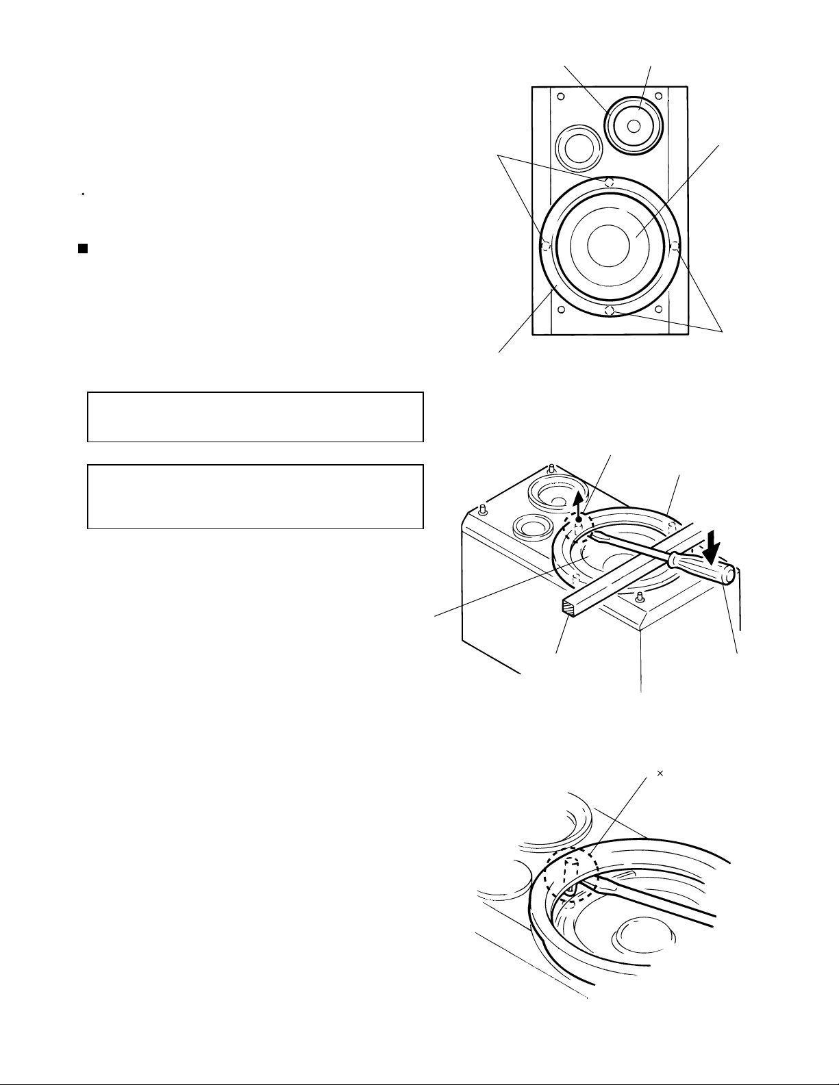
Removing the speaker (woofer)
(See Fig.1,3 to 5)
1.
Insert a screwdriver under the ornament grille
attached to the woofer.
2.
Pull out the ornament grille with each boss by means
of a lever as shown in Fig.2.
ATTENTION:
ATTENTION:
3.
Remove the four screws A and the woofer from the
body. Disconnect the wire from the speaker
terminals.
As the ornament grille is damaged,
replace it with the woofer.
When replacing the ornament grille,
make sure the boss with adequate
amount of bond.
Ornament grille
Boss
Ornament grille
Tweeter
Woofer
Boss
Fig.1
Boss
Ornament grille
Push
Woofer
Stick
Driver
Fig.2
Boss 4
Fig.3
1-29
Page 30
MX-S6MD
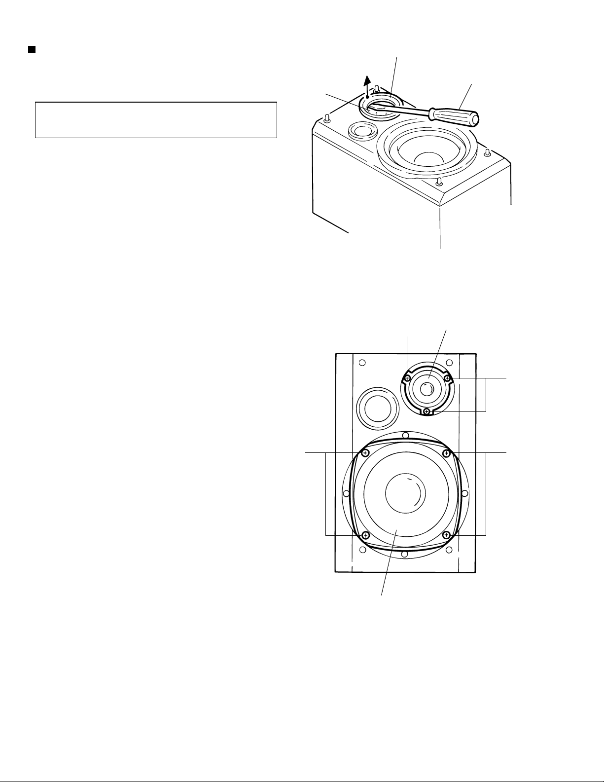
Removing the speaker (tweeter) (See Fig.4 and 5)
1.
Insert a screwdriver under the ornament grille and
remove it from the body.
ATTENTION:
3.
Remove the three screws B and the tweeter from
the body. Disconnect the wire from the speaker
terminals.
As the ornament grille is damaged,
replace it with the tweeter.
Tweeter
Ornament grille
Fig.4
B
Driver
Tweeter
Woofer
B
AA
Fig.5
1-30
Page 31
MX-S6MD
Adjustment method
This model is auto adjust system.
MD TEST MODE 1
1.Setting the TEST MODE1
(CAUTION) MD mode should NO
DISC condition, when POWER
ON to not read TOC.
Press [STOP key] and
[CANCEL key] together,
and connect the power cord.
LCD indication
MD TEST MODE 1
Setting the MD TEST MODE1
by press [POWER key]
LCD indication
[HELLO] then
[MD TEST MODE 1]
3.Laser power adjustment
Insert the sensor
of laser power meter
Press [ 2 key ] of
Remote controller
LCD indication
L.POWER PLAY
Adjust the PLAYBACK
laser power
Laser power up by [ key]
of Remote controller
LCD indication
L.POWER UP
0.68mW Adjustment
Press [STOP key] of
Remote controller
Playback laser power
adjustment complete
Laser power down by [ key]
of Remote controller
LCD indication
L.POWER DOWN
Setting OK
2.Initialize the EEPROM
Setting the MD TEST MODE 1
Press [REC PAUSE key]
of the Remote controller
LCD indication
DATA INITIAL
Initialize OK
Press [ 4 key] of
Remote controller
LCD indication
L.POWER REC
Adjust the RECORDING
laser power
Laser power up by [ key]
of Remote controller
LCD indication
L.POWER UP
6.23mW Adjustment
Press [STOP key] of
Remote controller
Press [EJECT key]
of main body
Laser power down by [ key]
of Remote controller
LCD indication
L.POWER DOWN
Adjustment complete
1-31
Page 32

MX-S6MD
4.Disc adjustment
This adjustment should done after laser power adjustment.
Insert
Pre-master disc
Complete TOC read
Press [MD key] of
the Remote controller
LCD indication
ON TUNING
Start auto adjustment
[CAUTION]
Please push the [STOP key] to remote control when the
LCD display becomes [NG ERROR], and push the
[MD key] to remote control again.
/
Adjustment
OK?
LCD indication
OK_TUNING
Eject the
Pre-master disc
Insert the
Recordable disc
Complete TOC read
Press [MD key] of
the Remote controller
LCD indication
ON TUNING
Start auto adjustment
LCD indication
NG_ERR _!
<Refer the NG code list>
<NG code list>
CODE
Adjustment NG section
00
Auto adjustment not complete
01
REST switch detection
02
FOCUS ON
03
PIT section EF balance, tracking offset adjustment
04
PIT section ABCD level (IV impedance) adjustment
05
PIT section focus servo AGC
06
PIT section tracking servo AGC
07
PIT section focus bias adjustment
08
GRV section EF balance, tracking offset adjustment
09
GRV section ABCD level (IV impedance) adjustment
0A
GRV section focus servo AGC
0B
GRV section tracking servo AGC
0C
GRV section focus bias adjustment
0D
Room temperature
0E
EEPROM writing
FF
Auto adjustment complete (OK)
1-32
Adjustment
OK?
LCD indication
OK_TUNING
Press [STOP key] of
the Remote controller
Press [EJECT key]
of the main body
Complete the adjustment
LCD indication
NG_ERR _!
<Refer the NG code list>
Page 33
MX-S6MD
5.Independent operation mode
In case the checking mode or adjustment
when occur the error at disc adjustment,
Independent mode into by select the key
before release the TERST MODE.
MD TEST MODE 2
1.Setting the TEST MODE 2
(CAUTION) MD mode should NO
DISC condition, when POWER
ON to not read TOC.
Press [STOP key] and
[CANCEL key] together,
and connect the power cord.
LCD indication
MD TEST MODE 1
Operation key
Remote controller [SLEEP]
Remote controller [6 key]
Remote controller [7 key]
Remote controller [8 key]
Remote controller [9 key]
Remote controller [STOP]
Main body [EJECT]
2.Indication the drift level of
the pickup adjustment value
TEST MODE 2
Insert the Pre-master disc
Read the TOC
Press [6 key] of the
Remote controller
MODE
Focus search [FOCUS_SEARCH]
Pit rough servo [P.R.SERVO]
Groove rough servo [GR.R.SERVO]
Tracking ON [TRACKING_ON]
Tracking OFF [TRACKING_OFF]
STOP [STOP]
EJECT [EJECT]
Setting the MD TEST MODE1
by press [POWER key]
LCD indication
[HELLO] then
[MD TEST MODE 1]
Setting the MD TEST MODE2
by press [STOP key] and
[TITLE/EDIT key] together
Setting OK
3.Indication the C1 ERROR
TEST MODE 2
Insert the recordable
disc (basically 74min.)
Read the TOC
Press [8 key] of
the Remote controller
LCD indication
[ _ ]
Adjustment value
IVR
TAG C
TBAL
LPOW
FBIA
FAGC
TEOF
SAGC
IVR (Pre-master, Recordable groove)
TRK AGC ( )
TRK BALANCE ( ) = 0
Laser power (Play power=0 Rec power)
Focus bias ( ) = 0
Focus AGC ( )
TE offset ( ) = 0
Sled AGC ( )
4.Release the MD TEST MODE
TEST MODE
Press [POWER key]
POWER OFF
Release the TEST MODE
LCD indication (change by each 10sec.)
[_ _ _ _ _]
LCD indication (change be each 10sec.)
[______ Times_]
1-33
Page 34
MX-S6MD
CD TEST MODE
CD section is no need the adjustment by design.
1.Setting the TEST MODE
Press [STOP key] and
[HIGH SPEED CD MD REC key]
of the main body together and
connect the power cord
LCD indication
CD TEST MODE
CD TEST MODE setting by
press [POWER key]
LCD indication
[HELLO] then
CD TEST MODE
Complete setting
2.Indication the C1 ERROR
TEST MODE
Read TOC
Press [1 key] of the
Remote controller ( x1 speed)
Playback each 10sec.
C1 ERROR q'ty indicate by 2byte
LCD indication (change each 10sec.)
[__________ __ ]
LCD indication (change each 10sec.)
[________ Times__]
3.Release the CD TEST MODE
TEST MODE
Press [2 key] of the
Remote controller ( x2 speed)
1-34
Press [POWER key]
Power to OFF
Release the TEST MODE
Page 35

LCD ALL INDICATION, TIME COMPRESSION TEST MODE
1.Setting the TEST MODE
POWER ON
Press [POWER key],[1 key] and
[STOP key] together of the
Remote controller (1st time)
MX-S6MD
LCD and LED are all ON
Full color LED is WHITE
Press [POWER key],[1 key] and
[STOP key] together of the
Remote controller (2nd time)
Inspection for static
electricity broken check mode
for full color LED (RED)
Press [POWER key],[1 key] and
[STOP key] together of the
Remote controller (3rd time)
Inspection for static
electricity broken check mode
for full color LED (GREEN)
Press [POWER key],[1 key] and
[STOP key] together of the
Remote controller (4th time)
Inspection for static
electricity broken check mode
for full color LED (BLUE)
(press any key) Change to normal indication
It can check for red color chip part
It can check for green color chip part
It can check for blue color chip part
Caution:Full color LED is keep white condition, when loop out by any key at test mode.
2.Fast forward of CLOCK/SLEEP TIMER
Including the ALL LED ON mode and Static electricity broken thes, clock count up is change to
1min. to 1sec.
Check for only [CLOCK mode] and [SLEEP TIMER].
3.Release the TEST MODE
TEST MODE is release by disconnect the AC power cord.
1-35
Page 36
MX-S6MD
RUNNING MODE
This running mode is a mode by which the recording is compulsorily deleted with ALL-ERASE after
U-TOC is written when the recording of MD ends, and the recording is repeated again.
This TEST MODE is continue recording (loop recording), it is for recording stop when MD end.
This TEST MODE is only can use manual operation recording [MD REC PAUSE]. CD synchro recording
(CD MD REC,BEST HIT REC,1CD MD REC) is not operate correctly.
1.Setting the TEST MODE
1:Setting normal speed recording mode by pressing together [POWER key], [2 key] and [STOP key]
of Remote controller.
2:If normal speed mode is default then change to high speed mode, press [HIGH SPEED CD>MD key] of
main body before recording start.
3:Once change to high speed mode, TEST MODE is continue until release.
4:Return to normal speed recording mode, it should release the TEST MODE then resetting the
TEST MODE.
(REMARKS) Case of CD high speed recording : After setting TEST MODE, if it need setting
CD play mode or repeat mode. Press [HIGH SPEED CD > MD key] setting high speed
mode. RUNNING MODE is start by REC STANDBY (indicate [RUNNING MODE] on LCD)
at [MD REC PAUSE key] then playback the CD.
(During recording, LCD indicate [RUNNING MODE])
2.Release the TEST MODE
Test mode is release by POWER OFF.
Indication the [CAUTION !] when abnormal
1.Detect the abnormal condition of stability power supply
Abnormal detection dine of the stability power supply(REG.) at CPU [SAFETY1~3] port (IC801:6,7,9pin),
when system CPU (IC801) supply voltage (US D5.6V) is normal condition.
Watching the abnormal at POWER ON condition, if detect the abnormal indicate [CAUTION!] and come
under stability power supply (8V/10V or 12V OR 6V), and indicate [DATA(HEX)] of the abnormal port
voltage then power off to forcibly.
Detect the abnormal condition of stability power supply is next.
[8V/10V] : SAFETY1 port (Power supply of full color LED/Power supply of CD mechanism)
[12V] : SAFETY2 port (Power supply for tuner module REG, MD mechanism REG, volume IC,
LPF IC and CD/MD SELECTOR)
[6V] : SAFETY3 port (Power supply for MD mechanism, power supply for OPT. module, power
supply for CD/OPT SELECTOR)
2.Abnormal detection of CD mechanism
(REMARKS) Safety port voltage at detect the abnormal condition.
DATA(HEX)
3FF~2D0
2CF~12C
12B~000
When detect the abnormal condition of CD mechanism, indicate [CAUTION ! ] and come under
condition and back light is change to [RED] forcibly.
PORT voltage
5.0~3.52V
3.515~1.456V
1.46V~0V
Detect condition
Abnormal (Power off at 1sec. forcibly)
Normal
Abnormal (Power off at 3sec. forcibly)
1-36
Indication when mechanism abnormal condition.
[CD INITIAL] : Abnormal condition when mechanism initialize after power cord to connect to
AC outlet then power to ON.
[CD MECH] : Abnormal condition when mechanism initialize at return operation, it is
Sub Tray Load/Unload operation, Lifter shift operation, or CAM operation
are defect.
[CD MECHA 5V] : Abnormal condition at 5V (LSI) internal the CD mechanism.
Page 37

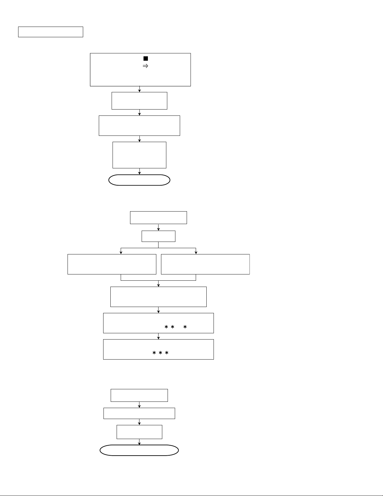
Flow of functional operation until TOC read (MD section)
Power ON
MD play Key
Check point
Slider turns REST
switch ON
Confirm that the voltage
at the pin 9 of CN408 are
0V.
MX-S6MD
Mechanism operation ON
Laser ON
Disc detection
Automatic tuning of
Focus S-curve amplitude
Disc is rotated
Focus servo ON
(Tracking servo ON)
Automatic tuning of
Focus error gain
Confirm that the voltage
at the pin 50 of IC500 are 4V.
Confirm that the Focus error
S-curve signal at the pin 34 of
IC310 is approx.2Vp-p.
It is confirmed that pin 2 of CN408
become 0V from VREF as an acceleration
pulse between about 400ms.
Automatic tuning of
Tracking error gain
TOC reading
Play a disc
Confirm that the eye-pattern
at the pin38 of IC310.
1-37
Page 38

MX-S6MD
Maintenance of laser pickup
(MD)
1. Cleaning of pickup lens
(1) Prior to changing the pickup, clean the pickup lens.
(2) For cleaning the lens, use the following cotton swab after
mearsing it in alcohol.
Product No : JCB-B4 Manufacturer : Nippon Cotton Swab
2. Confirmation of the service life of laser
diode when the service life of the laser
diode has been exhausted, the following
symptoms will appear.
(1) Recording will become impossible.
(2) The RF output (EFM output and eye-pattern amplitude)
will become lower.
(3) The drive current required for light emitting of laser diode
will be increased.
Replacement of laser pickup
(MD)
Change the MD pickup by referring to
"Removing the MD pickup" in the
disassembly method.
Set the pickup to [TEST] mode according
to the procedures described in the
adjustment method.
Adjust the laser power.
Completion the disc.
Confirm the service life according to the following flow chart.
Is the
recording power
(6.23mW) output with
the laser power under
test mode?
YES
The drive current
of laser diode 120mA
or less?
YES
O.K.
NO
Change
NO
Change
3. Method of measuring the drive current
of laser diode
When the voltage measured at each side of R337,
it become 120mV or over, the service life of laser
diode is judged to have been exhausted.
Completion of changing the MD pickup.
CAUTION
Since this system is designed to perform magnetic
recording, the laser power ten times or over of the
conventional MD player will be output. Therefore, be
sure to perform not only adjustment and operation
of this system so carefully as not to directly look at
the laser beam or touch on the body.
4.Semi-solid state resistors on the
APC board.
The semi-solid state resistor on the APC board
attached to the pickup is used for adjusting the laser
power. Since these resistor should be adjusted in
pair according to the characteristics of the optical
block, be sure not touch on the resistors.
Since the service life of the laser diode will be
exhausted when the laser power is low, it is
necessary to change the pickup.
Meanwhile, do not pickup.
Otherwise, the pickup will be damaged due to over
current.
1-38
Page 39

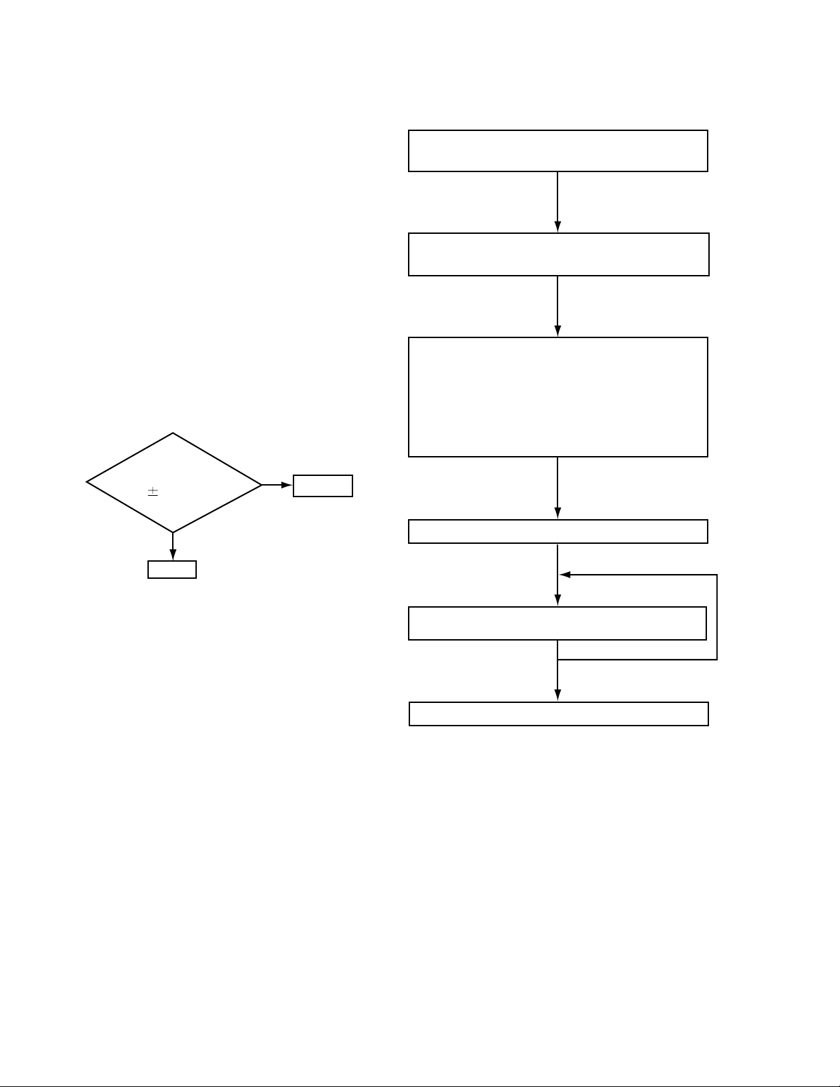
Flow of functional operation until TOC read (CD section)
Check Point
Power ON
Disc play Key
REST switch to ON
by slider
TE offset auto adjust
Check that the voltage at
the pin33 of IC701 or pin3
of CN694 is 0V(a moment)?
MX-S6MD
Tracking error waveform at TOC reading
IC601
25pin(TE)
Approx
1.8V
VREF
Disc status
to rotate
Automatic measurement
at TE amplitude and
TE balance
Approx.3sec
TE servo OFF
start
TE servo
ON start
Disc to be
braked to stop
TOC reading
finishes
500mv/div
2ms/div
Laser ON
Disc detection
FO offset auto adjust
Auto measure FOS
curve amplitude
Disc rotated
Focus servo ON
(tracking servo ON)
Auto measure
TE amplitude
Auto measure
TE balance
Check the voltage at the pin40
of IC603 + side is +5V?
Confirm that the Focus error
S-curve signal at the pin28 of
IC603 is approx.2Vp-p
Confirm that the signal form
pin24 of IC603 is 0V as a
accelerated pulse during
approx.400ms.
Confirm the waveform of the
tracking error signal at the
pin25 of IC601.
(about 1.8Vpp)
FO balance auto adjust
FO gain auto adjust
TE gain auto adjust
TOC read
Play
Confirm the eye-pattern
at the lead of TP602.
1-39
Page 40
MX-S6MD
Maintenance of laser pickup
(CD)
(1) Cleaning the pickup lens
Before you replace the pickup, please try to
clean the lens with a alcohol soaked cotton
swab.
(2) Life of the laser diode
When the life of the laser diode has expired,
the following symptoms will appear.
(1) The level of RF output (EFM output : amplitude
of eye-pattern) will below.
Is RF output
1.25 0.22VP-P?
NO
Change
Replacement of laser pickup
(CD)
Turn of the power switch and, disconnect the
power cord from the AC outlet.
Replace the pickup with a normal one.(Refer
to "Pickup Removal" on the previous page)
Plug the power cord in, and turn the power on.
At this time, check that the laser emits for
about 3seconds and the objective lens moves
up and down.
CAUTION : Do not observe the laser beam
directly.
YES
O.K.
(3) Semi-fixed resistor on the APC board
The semi-fixed resistor on the APC board
which is attached to the pickup is used to
adjust the laser power.
Since this adjustment should be performed
to match the characteristics of the whole
optical block, do not touch the semi-fixed
resistor.
If the laser power is lower than specified
value, the laser diode is almost worm out,
and the pickup should be replaced.
If the semi-fixed resistor is adjust while the
pickup is functioning normally, the laser
pickup may be damaged due to excessive
current.
Play disc
Check the eye-pattern at TP602.
Finish
1-40
Page 41

Description of major ICs
AK4519VF-X (IC480) : A / D D / A converter
1.Pin layout
1
2
3
4
5
6
7
8
9
10
11
12
24
23
22
21
20
19
18
17
16
15
14
13
MX-S6MD
2.Block diagram
AINL
VCML
AINR
VCMR
VRAD
ARDV
VCOM
AOUTL
AOUTR
3.Pin Function
Pin
Symbol I/O Function
NO.
1
2
3
4
5
6
7
8
9
10
11
12
13
14
15
16
17
18
19
20
21
22
23
24
VRDA
VRAD
AINR
VCMR
VCML
AINL
PWAD
PWDA
MCLK
LRCK
SCLK
SDTO
DGND
VD
SDTI
CMODE
DEM1
DEM0
AOUTL
AOUTR
VCOM
AGND
VB
VA
Voltage Reference Input Pin for DAC, VA
I
Voltage Reference Input Pin for ADC, VA
I
RCH Analog Input Pin
I
Rch Common Voltage Output Pin, 0.45xVA
O
Lch Common Voltage Output Pin, 0.45xVA
O
Lch Analog Input Pin
I
ADC Power-Down Mode Pin "L":Power Down
I
DAC Power-Down Mode Pin "L":Power Down
I
Master Clock Input Pin
I
Input/Output Channel Clock Pin
I
Audio Serial Data Clock Pin
I
Audio Serial Data Output Pin
O
Digital Ground Pin
Digital Power Supply Pin
Audio Serial Data Input Pin
I
Master Clock Select Pin
I
De-emphasis Frequency Select Pin
I
De-emphasis Frequensy Select Pin
I
Lch Analog Output Pin
O
Rch Analog Output Pin
O
Common Voltage Output Pin, 0.45xVA
O
Analog Ground Pin
Substrate Pin
Analog Power Supply Pin
-
VA AGND VB VD DGND
Decimation
Modulator
Filter
Decimation
Modulator
Filter
Common Voltage
LPF
LPF
Modulator
Modulator
8x
Interpolator
8x
Interpolator
PWAD PWDA
Clock
Divider
Serial I/O
Interface
MCLK
CMODE
LRCK
SCLK
SDTO
SDTI
1-41
Page 42
MX-S6MD
AN8849SB-W (IC601) : Head amp
1.Pin layout
2.Block diagram
36
35
34
33
32
GCTRL
FBAL
AGCEQ
DET
171098653
Substraction
Substraction
11 12
DET
BDO
OFTR
13
14
15
16
29
28
1-42
31
TBAL
21 23 25 2724 26
30
Page 43

3.Pin Function
Pin
Symbol Function
NO.
1
2
3
4
5
6
7
8
9
10
11
12
13
14
15
16
17
NRFDET
18
19
20
21
22
23
24
25
26
27
28
29
30
31
32
33
34
35
36
PD
LD
RFN
Vcc1
RFOUT
EQSW
Vcc2
RFC
CAGC
ARF
CEA
ENV
CBDO
BDO
COFTR
OFTR
GND
LDON
VREF1
CROSS
VREF2
CCRS
TEN
TEOUT
FEN
FEOUT
GCTRL
FBAL
TBAL
E
F
D
B
C
A
Photo detector signal input.
Laser diode drive terminal.
RF amp negative input terminal.
Power supply terminal.
Equaruzer connect terminal.
Power supply terminal.
RF AGC input terminal.
RF AGC filter connect terminal.
ARF output terminal.
3T envelope detect filter terminal.
Envelope detect output circuit.
Low level DO detect connect terminal.
DO detect signal output terminal.
OFF TRACK detect signal connect terminal.
OFF TRACK detect signal output terminal.
RF signal amp. detection output.
Ground.
LD APC ON / OFF select.
Reference voltage output terminal.
CROSS detect signal output terminal.
Reference voltage output terminal.
CROSS detect filter connect terminal.
Tracking error output terminal.
TE amp.negative input terminal.
FE amp.negative input terminal.
Focus error output terminal.
Focus gain, tracking gain adjust control signal inout terminal.
Focus barance adjust control input terminal.
Tracking barance adjust control input terminal.
Connect PDIC.
Connect PDIC.
Connect PDIC.
Connect PDIC.
Connect PDIC.
Connect PDIC.
Connect PDIC.
MX-S6MD
TC4066BP / N / (IC673) : Switch
1.Pin layout & block diagram 2.The truth circuit
IN/OUT1
OUT/IN1
OUT/IN2
IN/OUT2
CONT2
CONT3
VSS
1
2
3
4
5
6
7
14
13
12
11
10
9
8
VDD
CONT1
CONT4
IN/OUT4
OUT/IN4
OUT/IN3
IN/OUT3
CONT
O/II / O
1-43
Page 44

MX-S6MD
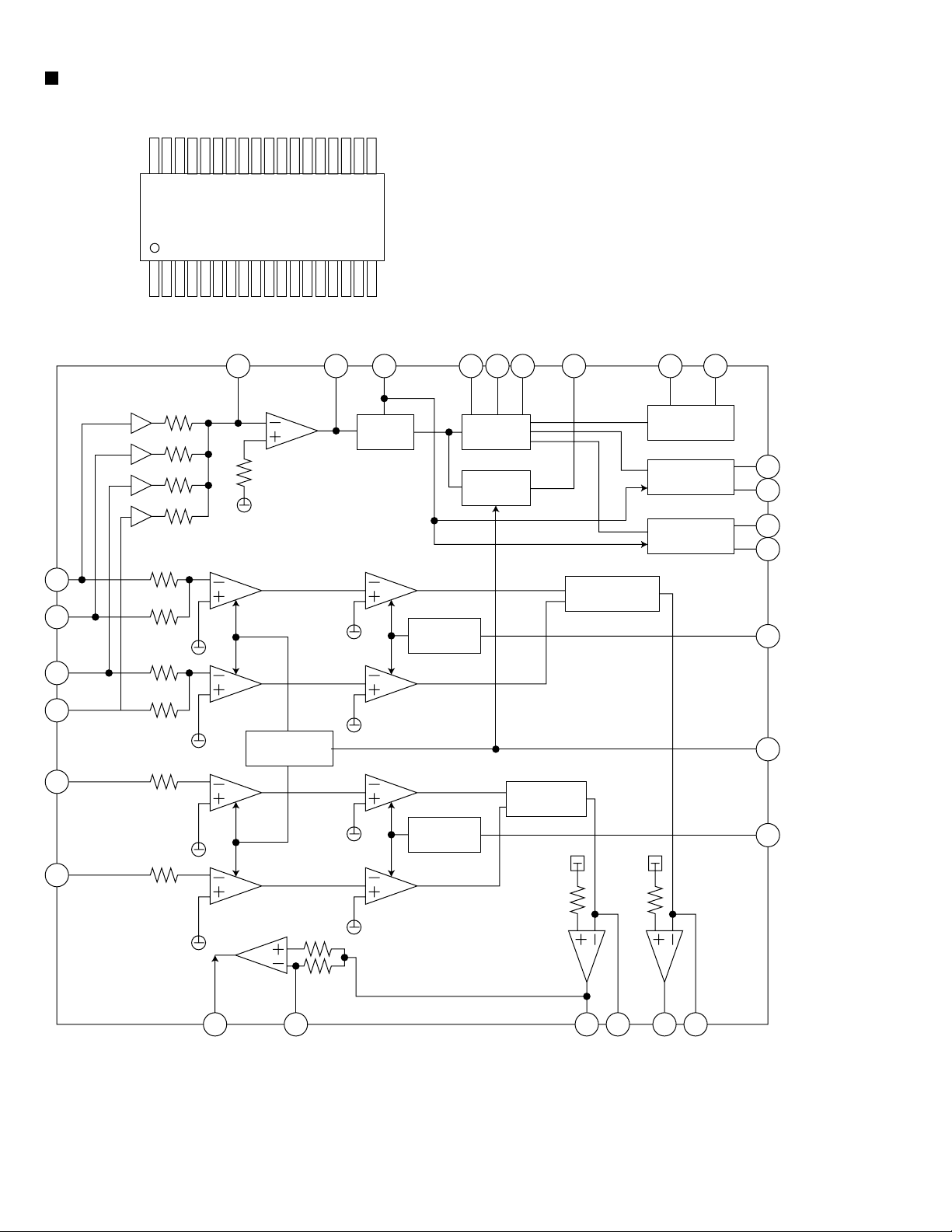
CXA2523AR (IC310) : MD servo
1.Block diagram
BOTM
ABCD34FE33AUX32ADFG31ADAGC30ADIN29ADFM28SE27CSLED26TE25WBLADJ
36 35
PEAK
37
38
RF
39RFAGC
40AGCI
41COMPO
42COMPP
43ADDC
44OPO
45OPN
46RFO
47MORFI
MORFO
48
2.Pin function
AGC, EQ
Comp
USER
USER
OP Amp
RF Amp
1 2
I
ADIP Amp TE/SE Amp
MUX FE Amp
Peak, Bottom Detector
ABCD Amp
3T Detector
I-V Amp APC
3VC4A5B6C7D8E9F10PD11
J
CPU
Command I/F
TEMP Amp
12
APC
APCREF
Vcc
24
23
3TADJ
22 EQADJ
21 VREF
20 F0CNT
19 XSTBY
18 XLAT
17 SCLK
16 SWDT
15 TEMP R
14 TEMP I
13 GND
Pin No.
1
2
3
4
5
6
7
8
9
10
11
12
13
14
15
16
17
18
19
20
Symbol
I
J
VC
A
B
C
D
E
F
PD
APC
APCREF
GND
TEMPI
TEMP R
SWDT
SCLK
XLAT
XSTBY
F0CNT
I/O
I-V converted RF signal I input.
I
I-V converted RF signal J input.
I
Vcc/2 voltage output.
O
A current input for main beam servo signal.
I
B current input for main beam servo signal.
I
C current input for main beam servo signal.
I
D current input for main beam servo signal.
I
E current input for side beam servo signal.
I
F current input for side beam servo signal.
I
Reflection light quantity monitor signal input.
I
Laser APC output.
O
Reference voltage input for the laser power intensity setting.
I
Connect to GND.
Connects the temperature sensor.
I
Connects the temperature sensor. outputs the reference voltage.
I
Data input for microcomputer serial interface.
I
Shift clock input for microcomputer serial interface.
I
Latch signal input for microcomputer serial interface.Latched when low.
I
Standby setting pin. Normal operation when high Standby when low.
I
Internal current source setting pin.
I
Function
1-44
Page 45

MX-S6MD
Pin No.
21
22
23
24
25
26
27
28
29
30
31
32
33
34
35
36
37
38
39
40
41
42
43
44
45
46
47
48
Symbol
VREF
EQADJ
3TADJ
Vcc
WBLADJ
TE
CSLED
SE
ADFM
ADIN
ADAGC
ADFG
AUX
FE
ABCD
BOTM
PEAK
RF
RFAGC
AGCI
COMPO
COMPP
ADDC
OPO
OPN
RFO
MORFI
MORFO
I/O
Reference voltage output.
O
Equalizer center frequency setting pin.
I/O
BPF3T center frequency setting pin.
I/O
Power supply.
BPF22 center frequency setting pin.
I/O
Tracking error signal output.
O
Connects the sled error signal LPF capacitor.
Sled error signal output.
O
ADIP FM signal output.
O
ADIP signal comparator input.
I
Connects the ADIPAGC capacitor.
ADIP2 binary value signal output.
O
13 output / temperature signal output. Switched with serial commands.
O
Focus error signal output.
O
Reflection light quantity signal output for the main beam servo detector.
O
RF/ABCD bottom hold signal output.
O
Peak hold signal output for the RF/ABCD signals.
O
RF equalizer output.
O
Connects the RFAGC capacitor.
RFAGC input.
I
User comparator output.
O
User comparator non-inverted input.
I
Connects the capacitor for ADIP amplifier feedback circuit.
I/O
User operational amplifier output.
O
User operational amplifier inverted input.
I
RF amplifier output. Eye pattern checkpoint.
O
Input of the groove RF signal with AC coupling.
I
Groove RF signal output.
O
Function
LB1641 (IC851,IC852) : DC motor driver
1. Pin layout
1 2 3 4 5 6 7 8 9
GND OUT1 P1
VZ IN1 IN2
2. Pin function
Input Output
IN1 IN2 OUT1 OUT2
0 0 0 0
1 0 1 0
0 1 0 1
1 1 0 0
VCC1
VCC2 P2
10
OUT2
CLOCKWISE
COUNTER-CLOCKWISE
Mode
Brake
Brake
1-45
Page 46
MX-S6MD
CXD2662R (IC350) : DSP
1.Pin layout
2.Block diagram
59
PCO
60
FILI
FILO
CLTV
EFM
RFI
ASYI
BIAS
61
62
100
57
54
56
PLL
COMP
75 ~ 51
76
~~
100
1 ~ 25
50
26
EFM / ACIRC
ENCODER / DECODER
OSCI
OSCO
XTSL
16 17 18 29
CLOCK
GENERATOR
each block
FS256
LRCK
XBCK
FS4
MDDT1
90 52
27 28
SHOCK RESISTANT
MEMORY CONTROLLER
12
XRAS
46
XCAS
44
XWE
4
4
47
43
14
15
XOE
A00~A11
D0~D3
XINT
TX
ASYO
ADFG
FGIN
SPFD
SPRD
F0CNT
APC
FE
TE
SE
PEAK
BOTM
ABCD
AUX1
DCHG
VC
ADIO
ADRT
ADRB
DTRF
CKRF
XLRF
53
78
95
94
93
79
77
66
75
74
63
64
65
67
76
68
69
71
72
82
81
80
ADIP DECODER
SPINDLE
SERVO
A/D
CONVERTER
ANALOG MUX
AUTO
SEQUENCER
ATRAC/ATRAC3
ENCODER/DECODER
SAMPLING
RATE
CONVERTER
SERVO
DSP
each block each block
CPU I/F
MONITOR
CONTROL
DIGITAL
AUDIO
I/F
SUBCODE
PROCESSOR
PWM
GENERATOR
DADT
26
ADDT
25
XBCKI
2
24
LRCKI
23
DATA I
22
DIN~DIN1
DOUT
21
12
11
84
88
89
86
85
92
91
83
DQSY
SQSY
LDDR
FFDR
FRDR
TFDR
TRDR
SFDR
SRDR
APCREF
4
1-46
10 7
XRST
5689 12 34 13
XLAT
SCLK
SWDT
SRDT
SENS
MNT0
MNT1
MNT2
MNT3
RECP
Page 47

3.Pin function
MX-S6MD
Pin No.
1
2
3
4
5
6
7
8
9
10
11
12
13
14
15
16
17
18
19
20
21
22
23
24
25
26
27
28
29
30
31
32
33
34
35
36
37
38
39
40
41
42
43
Symbol
MNT0
MNT1
MNT2
MNT3
SWDT
SCLK
XLAT
SRDT
SENS
XRST
SQSY
DQSY
RECP
XINT
TX
OSCI
OSCO
XTSL
DIN0
DIN1
DOUT
DATA I
LRCKI
XBCKI
ADDT
DADT
LRCK
XBCK
FS256
DVDD
A03
A02
A01
A00
A10
A04
A05
A06
A07
A08
A11
DVSS
XOE
I/O
I/O
Monitor output.
O
Monitor output.
O
Monitor output.
O
Monitor output.
I
Data input for microcomputer serial interface.
I
Shift clook input for microcomputer serial interface.
I
Latch input for microcomputer serial interface.Latched at the falling edge.
O
Data output for microcomputer serial interface.
O
Outputs the internal status corresponding to the microcomputer serial
Function
interface address.
I
Reset input. Low : reset
O
Disc subcode Q sync / ADIP sync output.
O
Subcode Q sync output in U-bit CD or MD format when the Digital In
source is CD or MD.
I
Laser power switching input.
High : recording power ; low ; playback power
O
Interruption request output. Low when the interruption status occurs.
I
Enable signal input for recoding data output. High : enabled
I
Crystal oscillation circuit input.
O
Crystal oscillation circuit output. (inverted output ofthe OSCI pin)
I
OSCI input frequency switching.
XTSL1(command) = low and XTSL = high : 512Fs (22.5792MHz)
XTSL1(command) = low and XTSL = low : 1024Fs (45.1584MHz)
XTSL1(command) = high : 2048Fs (90.3168MHz)
I
Digital audio interface signal input 1.
I
Digital audio interface signal input 2.
O
Digital audio interface signal output.
I
Test pin. Connect to GND.
I
Test pin. Connect to GND.
I
Test pin. Connect to GND.
I
Data input from A / D converter.
O
REC monitor output / decoded audio data output.
O
LA clock (44.1kHz) output to the external audio block.
O
Bit clock (2.8224kHz) output to the external audio block.
O
256Fs output.
-
Digital power supply.
O
External DRAM address output.
O
External DRAM address output.
O
External DRAM address output.
O
External DRAM address output.
O
External DRAM address output.
O
External DRAM address output.
O
External DRAM address output.
O
External DRAM address output.
O
External DRAM address output.
O
External DRAM address output.
O
External DRAM address output.
-
Digital ground.
O
External DRAM output enable.
1-47
Page 48

MX-S6MD
Pin No.
44
45
46
47
48
49
50
51
52
53
54
55
56
57
58
59
60
61
62
63
64
65
66
67
68
69
70
71
72
73
74
75
76
77
78
79
80
81
82
83
84
85
86
87
88
89
90
Symbol
XCAS
A09
XRAS
XWE
D1
D0
D2
D3
MDDTI
ASYO
ASYI
AVDD
BIAS
RFI
AVSS
PCO
FILI
FILO
CLTV
PEAK
BOTM
ABCD
FE
AUXI
VC
ADIO
AVDD
ADRT
ADRB
AVSS
SE
TE
DCHG
APC
ADFG
F0CNT
XLRF
CKRF
DTRF
APCREF
LDDR
TRDR
TFDR
DVDD
FFDR
FRDR
FS4
I/O
O
External DRAM CAS output.
O
External DRAM address output.
O
External DRAM RAS output.
O
External DRAM write enable.
I/O
External DRAM data bus.
I/O
External DRAM data bus.
I/O
External DRAM data bus.
I/O
External DRAM data bus.
I
MD-DATA mode 1 switching input. (Low : normal mode ; high : MD-DATA mode 1)
O
Playback EFM full-swing input. (Low : vss ; jigh : Vdd)
I
Playback EFM comparator slice voltage input.
-
Analog power supply.
I
Playback EFM comparator bias current input.
I
Playback EFM RE signal input.
-
Analog ground.
O
Phase comparison output for master PLL of playback digital PLL and recording
Function
EFM PLL.
I
Filter input for master PLL of playback digital PLL and recording EFM PLL.
O
Filter output for master PLL of playback digital PLL and recording EFM PLL.
I
Internal VCO control voltage input for master PLL of playback digital EFM PLL and
recording EFM PLL.
I
Peak hold signal input for quantity of light.
I
Bottom hold signal input for quantity of light.
I
Signal input for quantity of light.
I
Focus error signal input.
I
Auxillary input 1.
I
Center voltage input.
I
Monitor output for A / D converter input signal.
-
Analog power supply.
I
Voltage input for the upper limit of the A / D converter operating range.
I
Voltage input for the lower limit of the A / D converter operating range.
-
Analog ground.
I
Sled error signal input.
I
Tracking error signal input.
I
Connect to he low-inpedance power supply.
I
Error signal input for laser digital APC.
I
ADIP binary FM signal (22.05 1kHz) input.
O
CXA2523 current source setting output.
O
CXA2523 control latch output. Latched at the falling edge.
O
CXA2523 control shift clook output.
O
CXA2523 control data output.
O
Referevce PWM output for laser APC.
O
PWM output for laser digital APC.
O
Tracking servo drive PWM output. ( )
O
Tracking servo drive PWM output. (+)
-
Digital power supply.
O
Focus servo drive PWM output. (+)
O
Focus servo drive PWM output. ( )
O
4Fs output. (176.4kHz)
1-48
Page 49

MX-S6MD
Pin No.
91
92
93
94
95
96
97
98
99
100
Symbol
SRDR
SFDR
SPRD
SPFD
FGIN
TEST1
TEST2
TEST3
DVSS
EFMO
I/O
O
Sled servo drive PWM output. ( )
O
Sled servo drive PWM output. (+)
O
Spindle servo drive output. (PWM ( ) or polarty)
O
Spindle servo drive output. (PWM (+) or PWM absolute value)
I
Spindle CAV servo FG input.
I
Test pin. Connect to GND.
I
Test pin. Connect to GND.
I
Test pin. Connect to GND.
-
Digital ground.
O
Low when playback ; EFM (encoded data) output when recording.
BD7910FV-X (IC450) : Pre driver
1.Block diagram
20 19 18 17 16 15 14 13 12 11
Function
- +
Vregin
1 2 3 4 5 6 7 8 9 10
- +
VG
SVcc
Pre driver
EFM
2.Pin function
Pin
Symbol Symbol
No.
1
Vreg IN
2
Reg GN
3
NC
4
VG
5
SVCC
6
PDGND
7
EFM
8
MUTE
9
NC
10
NC
I/O I/O
Regulator input and regulator
I
power supply
Regulator GND
Non connect
Voltage input for power MOS drive
I
EFM high level output voltage
O
Pre-driver GND
EFM signal input
I
Mute control (Low active)
I
Non conncet
O
Non connect
O
Function Function
Pin
No.
11
12
13
14
15
16
17
18
19
20
Mute
NC
VOD2
VSS
VOD1
VOS1
VDD
VOS2
Reg DRV
Reg OUT
Reg NF
-
Non connect
O
Sync.output (Lower power MOS,drain)
-
"H"bridge GND (Lower power MOS,source)
O
Sync.output (Lower power MOS,drain)
O
Source output (Upper power MOS,source)
-
"H" bridge power supply terminal
(Upper power MOS,source)
O
Source output (Upper power MOS,source)
O
External PNP drive output for regulator
O
Reglator output (Emitter follower output)
-
Regulator feedbaack terminal
1-49
Page 50

MX-S6MD
HD6432345A15FA (IC500) : MD servo control
1.Pin layout
1
~
25
2.Pin function (1 / 2)
PIN No. I/O
1
2
3
4
5
6
7
8
9
10
11
12
13
14~16
17
18
19
20
21
22,23
24
25
26
27
28
29
30
31
32
33
34
35,36
37
38
39
40
41~44
45~48
49
50
I
O
O
O
-
-
O
O
COMMAND
I
I
COMCLK
I
O
-
-
O
O
O
O
MODCHG
O
-
MONIDATA
O
MONICLK
O
MONILAT
O
O
O
O
O
I
I
-
I
I
O
100 ~ 76
75
~
51
26 ~ 50
Symbol Function
DO
DI
SCL
CS
STSRDY
NC
VSS
STATUS
SWDT
Data input for EEPROM.
Data input for EEPROM.
Clock output for EEPROM.
Chip select for EEPROM 1.
Non connected.
Non connected.
Ground
Status output for host.
Data output to CXD2662R.
Command input from host.
SRDT
Data input from CXD2662R.
Clock input from host.
SCLK
NC
POWER
VSS
PWAD
PWDA
EMPHA
NC
MODON
Serial clock output to CDX2662R.
Non connected.
Power supply.
Ground
AD power control output.
DA power control output.
Emphasis control output.
Non connected.
High frequency ON / OFF output.
High frequency power select output.
NC
Non connected.
Data output for debag / test mode.
Clock output for debag / test mode.
Latch output for debag / test mode.
XTSL
VSS
TX
NC
RECP
NC
XRST
SENS
XLAT
VCC
MNT3~0
CAM4^1
VSS
DRVON
Input frequency select output to CXD2662R.
Ground
Write data output permission to CXD2662R.
Non connected.
Recording power output to CXD2662R.
Non connected.
LSI reset output to CXD2662R.
Monitor input from CXD2662R.
Write protect switch input.
Power supply.
LSI monitor signal from CXD2662R.
Mechanism position detect input.
Ground
4ch CLV drive power save.
1-50
Page 51

2.Pin function(2/2)
Pin No. I/OSymbol Function
46
47
48
49
50
51
52
53
54
55
56
57
58
59
60
61
62
63
64
65
66
67
68
69
70
71
72
73~78
79
80
81
82
83
84
85
86
87
88
89
90
91
92
93
94
95
96
97~99
100
COMM IN
COMM CLOCK
COMM PANEREQ
COMM RESET
TUNER DATA INPUT
TUNER CLOCK
TUNER CE
TUNER MPX
TUNER TUNED
TUNER MUTE
-
-
SPEAKER RELAY
AMP SOURCE MUTE
AMP LINE OUT MUTE
AMP STANDBY
AMP SOROUND ON/OFF
AMP SOURCE CD/MD
MD DIGITAL CD/AUX
-
-
AMP TDA7439CLOCK
AMP DATA
AMP POWER
AMP TR.SWITCH
AMP VOLUME JOG-1
AMP VOLUME JOG-2
-
AMP PROTECT
AMP INH
AMP BAND-1(CS)
AMP BAND-2(CS)
-
-
TUNER power
JOY A+H(SW1)
JOY B+G(SW1)
JOY C+F(SW1)
JOY D+E(SW1)
JOY COM1(SW1)
JOY COM2(SW1)
-
-
DAVss
JOY PUSH(SW2)
-
DAVdd
I
Common in control signal input terminal
O
Common clock signal output terminal
O
Common panel regulator signal output terminal
O
Common reset signal output terminal
I/O
Tuner data input terminal
O
Tuner clock signal output terminal
O
Tuner chip enable output terminal
I
Tuner MPX signal input terminal
I
Tuner tuned signal input terminal
O
Tuner mute signal output terminal
-
Non connect
-
Non connect
O
Speaker mute signal output terminal
O
Amp mute signal output terminal
O
Amp line out mute signal output terminal
O
Amp standby signal output terminal
O
Surround ON/OFF signal control terminal
O
Amp source CD/MD select signal control terminal
O
MD digital CD/AUX select signal control terminal
-
Non connect
-
Non connect
O
IC671 clock signal output terminal
O
Amp data signal control terminal
O
Amp power signal control terminal
O
TR switch control terminal
I
JOG-1 control terminal
I
JOG-2 control terminal
-
Non connect
I
Amp protect signal control terminal
I
Amp inhibit signal control terminal
-
Non connect
I
BAND-1 signal control terminal
I
BAND-2 signal control terminal
-
Non connect
-
Non connect
O
Tuner power supply signal control terminal
I
JOY signal control terminal[
I
JOY signal control terminal[
I
JOY signal control terminal[
I
JOY signal control terminal[
I
JOY signal control terminal[
I
JOY signal control terminal[
-
Non connect
-
Non connect
-
Connect to GND
I
JOY signal control terminal[
-
Non connect
-
DA power supply
MX-S6MD
1-51
Page 52

MX-S6MD
MN662748RPM (IC651) : Digital servo & digital signal processer
1. Pin layout
2.Block diagram
LRCKIN(MSEL)
BCLK(SSEL)
SRDATAIN
(PSEL)
IOSEL
CLVS
CRC
BLKCK
CLDCK
SBCK
SUBC
DEMPH
RESY
FLAG6(RESY)
SSEL
SQCK
SUBQ
AVDD2
AVDD2
PCK
EFM
PLLF
DSLF
IREF
DRF
ARF
RSEL
PSEL
MLD
MCLK
MDATA
CK384(EFM)
VCOF
BYTCK
SMCK
FCLK
CSEL
MSEL
X2
X1
ÊSTAT
DIGITAL
DEEMPHSIS
SUB
CODE
BUFFER
DSL.
PLL
VCO
VCO
ITUNING
GENERATION
PITCH
CONTROL
20 ~ 1
21
~
40
41 ~ 60
8TIMES
OVER SAMPUNC
DIGITAL FILTER
EFM
DEMODULATION
SYNC
INTERPOLATION
SUBCODE
DEMODULATION
MICRO
COMPUTER
INTERFACE
COVERTER
A/D
80
~
61
CIRC
ERROR
CORRECTION
DEINTERLEVE
CLV
SERVO
1BIT
DAC
LOGIC
S
16k
SRAM
INPUT
PEM
(R)
PEM
(L)
D/A
CONVERTER
OUTPUT
DIGITAL
AUDIO
INTERFASE
DIGITAL
AUDIO
INTERFASE
INTER POLATION
SOFT MUTING DIGITAL
ATTENUATION
PEAK DETECTIVE
AUTO CUE
PORT
SERVO
TIMING GENERATOR
AVSS1
AVDD1
OUTR
OUTL
FLAG
IPFLAG
TX
ECM
PC
LRCK
SRDATA
BCLK
DMUTE
TRKV
KICK
VREF
TRVSTR
ECS
TVD
TRD
FOD
TBAL
FBAL
TOFS
TES
/TLOCK
/FLOCK
PLAY
LDON
WVEL
SENSE
1-52
D
/
D
V
V
V
R
V
S
D
D
S
S
S
D
D
T
S
1
1
F
/
E
T
E
S
T
R
T
F
E
E
N
V
T
R
C
R
S
B
V
D
D
O
E
T
/
R
F
D
E
O
F
T
Page 53

3. Pin function
Pin
No.
1
2
3
4
5
6
7
8
9
10
11
12
13
14
15
16
17
18
19
20
21
22
23
24
25
26
27
28
29
30
31
32
33
34
35
36
37
38
39
40
Dymbol
BCLK
LRCK
SRDATA
DVDD1
DVSS1
TX
MCLK
MDATA
MLD
SENSE
FLOCK
TLOCK
BLKCK
SQCK
SUBQ
DMUTE
STATUS
RST
SMCK
PMCK
TRV
TVD
PC
ECM
ECS
KICK
TRD
FOD
VREF
FBAL
TBAL
FE
TE
RF ENV
VDET
OFT
TRCRS
RFDET
BDO
LDON
I/O
O
O
O
O
I
I
I
O
O
O
O
I
O
O
I
O
O
O
O
O
O
O
O
O
O
Function
Not used
Not used
Not used
I
Power supply (Digital)
I
Connected to GND
Digital audio interface output
CPU command clock signal input
(Data is latched at signal's rising point)
CPU command data input
CPU command load signal input
Sense signal output
Focus lock signal output Active :Low
Tracking lock signal output Active :Low
sub-code/block/clock signal output
Outside clock for sub-code Q resister input
Sub-code Q -code output
I
Connected to GND
Status signal
(CRC,CUE,CLVS,TTSTOP,ECLV,SQOK)
Reset signal input (L:Reset)
I
Not used
I
Not used
Traverse enforced output
Traverse drive output
I
Not used
Spindle motor drive signal (Enforced
mode output) 3-State
Spindle motor drive signal (Servo error
signal output)
Kick pulse output
Tracking drive output
Focus drive output
Reference voltage input pin for D/A
I
output block (TVD,FOD,FBA,TBAL)
Focus Balance adjust signal output
Tracking Balance adjust signal output
Focus error signal input (Analog input)
I
Tracking error signal input (Analog input)
I
I
RF envelope signal input (Analog input)
Vibration detect signal input (H:detect)
I
Off track signal input (H:off track)
I
Track cross signal input
I
RF detect signal input (L:detect)
I
BDO input pin (L:detect)
I
Laser ON signal output (H:on)
Pin
No.
41
42
43
44
45
46
47
48
49
50
51
52
53
54
55
56
57
58
59
60
61
62
63
64
65
66
67
68
69
70
71
72
73
74
75
76
77
78
79
80
Symbol
TES
PLAY
WVEL
ARF
IREF
DRF
DSLF
PLLF
VCOF
AVDD2
AVSS2
EFM
PCK
PDO
SUBC
SBCK
VSS
XI
X2
VDD
BYTCK
CLDCK
FLAG
IPPLAG
FLAG
CLVS
CRC
DEMPH
RESY
IOSEL
TEST
AVDD1
OUT L
AVSS1
OUT R
RSEL
CSEL
PSEL
MSEL
SSEL
I/O
Tracking error shunt signal output (H:shunt)
O
I
Not used
I
Not used
I
RF signal input
Reference current input pin
I
Bias pin for DSL
I
I/O
Loop filter pin for DSL
Loop filter pin for PLL
I/O
I
Not used
I
Power supply (Analog)
Connected to GND (Analog)
Not used
II I
Not used
I
Not used
I
Not used
I
Not used
Connected to GND (for X'tal oscillation
I
circuit)
Input of 16.9344MHz X'tal oscillation circuit
I
Output of X'tal oscillation circuit
O
I
Power supply (for X'tal oscillation circuit)
I
Not used
I
Not used
I
Not used
I
Not used
I
Not used
I
Not used
I
Not used
Not used
I
Not used
III
pull up
pull up
Power supply (Digital)
Lch audio output
O
I
Connected to GND
Rch audio output
O
II
pull up
Connected to GND
I
Connected to GND
I
Connected to GND
I
Pull up
Function
MX-S6MD
1-53
Page 54

MX-S6MD
UPD780024AGKB08 (IC251) : Unit micon
1. Pin layout
64 ~ 49
1
48
~
16
17 ~ 32
2. Pin function (1/2)
Pin
No.
Symbol I/O Function
1
E2SCK
2
E2SDL
3
4
5
6
7
8
9
10
11
12
13
14
15
16
17
18
19
20
21
22
23
24
25
26
27
28
29
30
31
32
MCS
MRDY
ITRVP3
ITRVP2
ITRVP1
ITRYSoc
VSSO
VDDO
/REST
CDEMP
CDTNO
CDCOPY
SUBQ
ICAMP1
SQCK
KCMND
M STAT
KCLK
RXDO
TXDO
ICAMP2
VDD1
AVSS
KEY1
KEY2
TRY3CLOSE
TRY3OPEN
TRY2CLOSE
TRY2OPEN
TRY1OPEN
~
33
O
EEPROM serial clock output
O
EEPROM serial data I/O
O
Synchronization / asynchronous system
I
Ready signal input terminal
O
Tray play position 3
O
Tray play position 2
O
Tray play position 1
I
Sub tray open/close
I
Ground
I
Reference power supply voltage
I
Rest switch
O
CD emphasis
I
CD track No. change
O
CD copy right or wrong
I
Sub Q data input
O
Cam position 1
O
Sub Q clock output
I
Command signal input
O
Status output
I
Command data clock input
I
(Command in)
O
(Status out)
O
Cam position 2
I
Reference power supply 1
I
Ground
I
key1 signal from running jig
I
Key2 signal from running jig
I
Tray 3 close signal input
I
Tray 3 open signal input
I
Tray 2 close signal input
I
Tray 2 open signal input
I
Tray 1 open signal input
1-54
Page 55

2. Pin function (2/2)
MX-S6MD
Pin
No.
Symbol I/O
33
TRY1CLOSE
34
AVREF
35
36
37
38
39
40
41
42
43
44
45
46
47
48
49
50
51
52
53
54
55
56
57
58
59
60
61
62
63
64
AVDD
/RESET
VSS1
FLAG
BLKCK
CAM_CW
CAM_CCW
ACT_CCW
ACT_CW
GCTRL
EQSW
ICAMP3
ICAMP4
/RESET
/DMUTE
/P.ON
M DATA
MCLK
SELECT
RUNDATA
RUNLOAD2
RUNLOAD1
RUNCLOCK
XT2
XT1
IC
X2
X1
S TAT
MLD
Function
I
Tray 1 close signal input
I
Reference power supply voltage
I
Reference power supply voltage
I
CD reset signal input
O
Non connect
I
Reference power supply voltage
I
No use ( for Flash micon)
O
X'tal osc output
I
X'tal osc input
I
Ground
O
FLAG for C1 error
O
Sub Q block clock signal output
O
Cam motor rotation clockwise
O
Cam motor rotation counter clockwise
O
Actuator motor rotation counter clockwise
O
Actuator motor rotation clockwise
I
Gain select 2/4 speed
I
Equalizer select 2/4 speed
I
Cam position 3
I
Cam position 4
O
Reset signal output
I
Status signal input
I
Digital mute signal input
I
Power on signal input
I
Command load signal input
I
Command data input
I
Command clock input
I
Communication select signal input
I
Running data input from running jig
I
Running load 2 signal input from running jig
I
Running load 1 signal input from running jig
I
Running clock signal input from running jig
1-55
Page 56
MX-S6MD
AK93C65AF-X (IC590) : EEPROM
1.Pin layout
PE
VCC
CS
SK
2.Block diagram
DI
CS
INSTRUCTION
1
2
3
4
8 PIN SOP
REGISTER
8
7
6
5
INSTRUCTION
GENERATION
NC
GND
DO
DI
DECODE,
CONTROL
AND
CLOCK
DATA
REGISTER
ADD.
BUFFERS
16
R/W AMPS
AND
AUTO ERASE
DECODER
DO
16
EEPROM
4096bit
256 x 16
SK
PE
3.Pin function
Pin no. Symbol
1 PE
2 VCC
3 CS
4 SK
5 DI
6 DO
7 GND
8 NC
Function
Program enable (With built-in pull-up resistor)
Power supply
Chip selection
Cereal clock input
Cereal data input
Cereal data output
Ground
No connection
NOTE : The pull-up resistor of the PE pin is about 2.5M (VCC=5V)
VREF
VPP SW
VPP
GENERATOR
1-56
Page 57

BR24C01AFV-W-X (IC201) : EEPROM
MX-S6MD
1.Pin layout
2.Block diagram
A0
1
A1
2
A2
3
Vcc WP SCL SDA
A0 A1 A2 GND
1kbit EEPROM ARRAY
7bit
ADDRESS
DECODER
CONTROL LOGIC
SLAVE/WORD
7bit
ADDRESS REGISTER
START
STOP
ACK
8bit
DATA
REGISTER
Vcc
8
WP
7
SCL
6
GND
4
HIGH VOLTAGE GEN.
3.Pin function
Pin name I/O
Vcc
GND
A0,A1,A2
SCL
SDA
WP
*1 An open drain output requires a pull-up resister.
-
-
IN
IN
IN / OUT
IN
Power supply
Ground (0v)
Slave address set
Serial clock input
Slave and word address,
serial data input, serial data output *1
Write protect input
Vcc LEVEL DETECT
Function
SDA
5
1-57
Page 58
MX-S6MD
HY51V17400CT-60 (IC390) : DRAM
1.Pin layout
Vcc
DQ0
DQ1
WE
RAS
A11
A10
A0
A1
A2
A3
Vcc
3.Block diagram
Vss
DQ3
DQ2
CAS
OE
A9
A8
A7
A6
A5
A4
Vss
2.Pin function
Pin Name Parameter
/RAS
/CAS
/WE
/OE
A0~A11
A0~A10
DQ0~DQ3
Vcc
Vss
NC
Row Address Strobe
Column Address Strobe
Write Enable
Output Enable
Address Input (4K Refresh Product)
Address Input (2K Refresh Product)
Data In/Out
Power (3.3V)
Ground
No Connection
DQ0 DQ1 DQ2 DQ3
4
4
WE
CAS
A0
A1
A2
A3
A4
A5
A6
A7
A8
A9
A10
*(A11)
CAS Clock
Generator
Cloumn Predecoder
(11/12)*
Refresh Counter
Refresh Counter
Address Buffer
Row Presecoder
(11/12)*
Data Input Buffer
DQ0~3 DQ0~3
44
(11/10)*
Decoder
(11/12)*
Row
Data Output Buffer
Column Decoder
Sense Amp
I/O Gate
Memory Array
4,194,304 x 4
OE
1-58
RAS
RAS Clock
Generator
X16 Parallel
Test
Substrate Bias
Generator
Vcc
Vss
Page 59

LA1838 (IC102): FM AM IF AMP&detector, FM MPX decoder
1. Block Diagram
MX-S6MD
30
ALC
BUFF
FM
S-METER
FM IF
1
2. Pin Function
Pin
Symbol
No.
FM IN
1
AM MIX
2
3
FM IF
AM IF
4
GND
5
6
TUNED
STEREO
7
8
VCC
9
FM DET
10
AM SD
FM VSM
11
AM VSM
12
13
MUTE
14
FM/AM
MONO/ST O
15
29
28
AM
OSC
SD
COMP
S-CLRVE
PM
DET
2
I/O
I
This is an input terminal of FM IF
REG
AM
MIX
AM/FM
IF-BUFF
3
27
FM
RF.AMP
AM IF
4
26
AGC
AM
S-METER
Function
DET
GND
5
signal.
This is an out put terminal for AM
O
mixer.
I
Bypass of FM IF
Input of AM IF Signal.
I
I
This is the device ground terminal.
When the set is tuning, this terminal
O
becomes "L".
O
Stereo indicator output. Stereo "L",
Mono: "H"
III
This is the power supply terminal.
I
FM detect transformer.
I
This is a terminal of AM ceramic filter.
O
Adjust FM SD sensitivity.
O
Adjust AM SD sensitivity.
I/O
When the signal of IF REQ of IC121(
LC72131) appear, the signal of FM/AM
IF output. //Muting control input.
Change over the FM/AM input.
I
"H" :FM, "L" : AM
Stereo : "H", Mono: "L"
25
TUNING
DRIVE
6
24
STEREO
DRIVE
7
22
23
P-DET
VCC
89
Pin
Symbol
No.
16
L OUT
17
R OUT
18
19
20
21
22
23
24
25
26
27
28
29
30
L IN
R IN
RO
LO
IF IN
FM OUT
AM DET
AM AGC
AFC
AM RF
REG
AM OSC
OSC BUFFER
21
DECODER
ANIT-BIRDIE
VCO
384KHz
10
20
STEREO
5N
SW
FF
38k
11
I/O
O
Left channel signal output.
O
Right channel signal output.
Input terminal of the left channel post
I
18
19
MUTE
FF
/
19k
2
12 13
FF
19k
/
LS
Function
17 16
PILOT
DET
14
AMP.
Input terminal of the right channel
I
post AMP.
Mpx Right channel signal output.
O
O
Mpx Left channel signal output.
I
Mpx input terminal
FM detection output.
O
AM detection output.
O
This is an AGC voltage input terminal
I
for AM
I
This is an output terminal of voltage
for FM-AFC.
AM RF signal input.
I
Register value between pin 26 and pin28
O
desides the frequency width of the
input signal.
I
This is a terminal of AM Local
oscillation circuit.
AM Local oscillation Signal output.
O
15
1-59
Page 60
MX-S6MD
LA6541-X (IC801) : Servo driver
1. Pin Layout & block diagram
Vcc Vref Vin4 Vg4 Vo8 Vo7
24 23
11k
ohm
22
21
20
19
Vcc
Gnd
Vo6 Vo5 Vg3 Vin3 Cd Res
18
17 16
- +
- +
Level
shift
Level
shift
11k
ohm
1
2
3456
Vcc Mute Vin1 Vg1 Vo1 Vo2 Vo3 Vo4 Vg2 Vin2 Reg
B T L
driver
B T L
driver
Gnd
B T L
driver
B T L
driver
7 8 9101112
Level
shift
Level
shift
2. Pin function
Pin
Symbol Function
No.
1
10
11
12
13
14
15
16
17
18
19
20
21
22
23
24
2
3
4
5
6
7
8
9
Vcc
Mute
Vin1
Vg1
Vo1
Vo2
Vo3
Vo4
Vg2
Vin2
Reg Out
Reg In
Res
Cd
Vin3
Vg3
Vo5
Vo6
Vo7
Vo8
Vg4
Vin4
Vref
Vcc
Power supply (Shorted to pin 24)
All BTL amplifier outputs ON/OFF
BTL AMP 1 input pin
BTL AMP 1 input pin (For gain adjustment)
BTL AMP 1 input pin (Non inverting side)
BTL AMP 1 input pin (Inverting side)
BTL AMP 2 input pin (Inverting side)
BTL AMP 2 input pin (Non inverting side)
BTL AMP 2 input pin (For gain adjustment)
BTL AMP 2 input pin
External transistor collector (PNP) connection. 5V power supply output
External transistor (PNP) base connection
Reset output
Reset output delay time setting (Capacitor connected externally)
BTL AMP 3 input pin
BTL AMP 3 input pin (For gain adjustment)
BTL AMP 3 output pin (Non inverting side)
BTL AMP 3 output pin (Inverting side)
BTL AMP 4 output pin (Inverting side)
BTL AMP 4 output pin (Non inverting side)
BTL AMP 4 output pin (For gain adjustment)
BTL AMP 4 output pin
Level shift circuit's reference voltage application
Power supply (Shorted to pin 1)
15
11k
ohm
14
13
RESET
Regulator
11k
ohm
out
Reg
In
1-60
Page 61
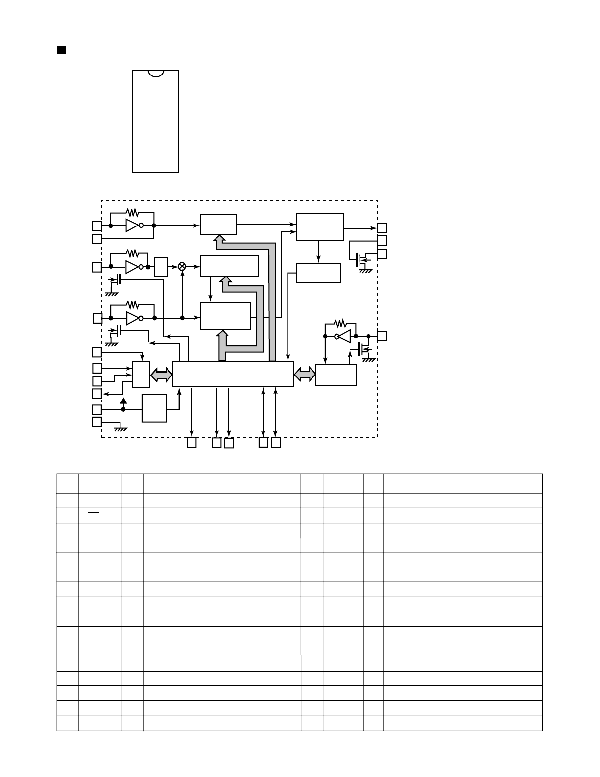
LC72136N (IC121) : PLL frequency synthesizer
1. Pin layout
FM/AM
CLOCK
FM/ST/VCO
AM/FM
2. Block diagram
XT
CE
DI
DO
SDIN
1
2
3
4
5
6
7
8
9
10
11
22
21
20
19
18
17
16
15
14
13
12
XT
GND
LPFOUT
LPFIN
PD
VCC
FMIN
AMIN
IFCONT
IFIN
MX-S6MD
1
22
16
15
3
4
5
6
17
21
3. Pin function
Pin
Symbol
No.
1
2
3
4
5
6
7
8
9
10
11
XT
FM/AM
CE
DI
CLOCK
DO
FM/ST/VCO
AM/FM
LW
MW
SDIN
Reference
Driver
Swallow Counter
1/2
C
2
B
I/F
Powe r
on
Reset
Function
I/O
X'tal oscillator connect (75kHz)
I
LOW:FM mode
O
When data output/input for 4pin(input) and
I
Swallow Counter
1/16,1/17 4bit
1/16,1/17 4bit
12bit
Programmable
DriverS
Data Shift Register & Latch
7821113
6pin(output): H
Input for receive the serial data from
I
controller
Sync signal input use
I
Data output for Controller
O
Output port
"Low": MW mode
O
Open state after the power on reset
O
Input/output port
I/O
Input/output port
I/O
Data input/output
I/O
Phase
Detector
Charge Pump
Unlock
Detector
Universal
Counter
Pin
Symbol
No.
12
IFCONT
13
14
15
16
17
18
19
LPFOUT
20
21
22
IFIN
AMIN
FMIN
VCC
PD
LPFIN
GND
XT
18
19
20
12
I/O
Function
IF counter signal input
I
IF signal output
O
Not use
-
AM Local OSC signal output
I
FM Local OSC signal input
I
Power suplly(VDD=4.5-5.5V)
When power ON:Reset circuit move
PLL charge pump output(H: Local OSC
O
frequency Height than Reference frequency.
L: Low Agreement: Height impedance)
Input for active lowpassfilter of PLL
I
Output for active lowpassfilter of PLL
O
Connected to GND
X'tal oscillator(75KHz)
I
1-61
Page 62
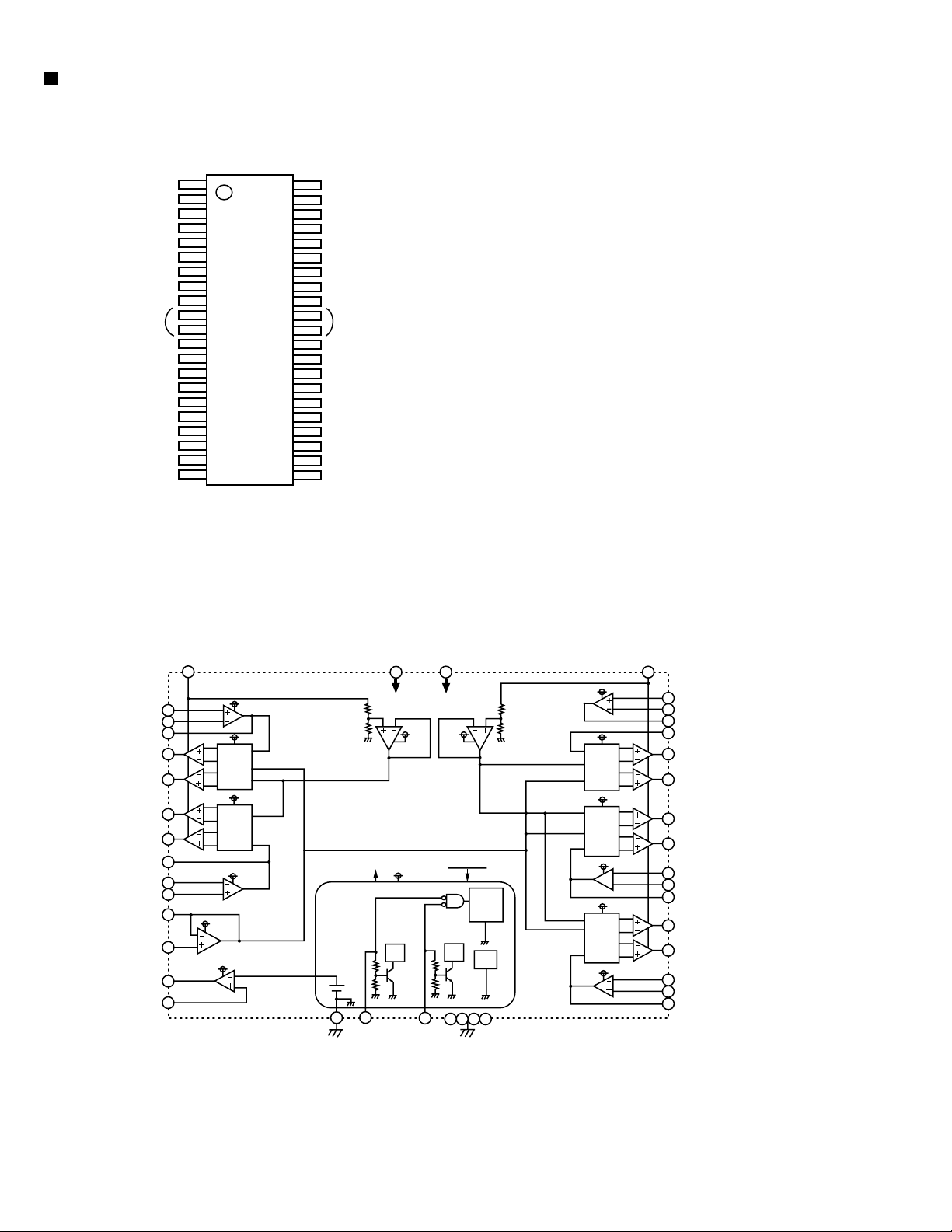
MX-S6MD
M63008FP-X (IC410) : 5ch Actuator driver
1.Pin layout
REG+
REGB
IN1+
VBS1
Vm1
IN1-
OUT1
VM1-
VM1+
GND
VM2+
VM2-
OUT2
IN2-
IN2+
MUTE1
MUTE2
SS,GND
VREF
VREFO
2.Block diagram
CH3IN
OUT3
IN3VBS2
Vm2
IN3+
N.C
VM3VM3+
GND
VM4+
VM4VM5+
VM5OUT5
IN5IN5+
IN4+
IN4OUT4
IN1+
IN1-
OUT1
VM1(+)
VM1(-)
VM2(+)
VM2(-)
OUT2
IN2-I
IN2+
VREFO
VREF
REGB
REG+
Vm1
5
VBS2
CH1
CH2
VBS1
VREF
X5
X5
E2
E1
VBS1
VBS1
VBS1
VBS1
1.25V
19 17
3
6
7
9
8
12
13
14
15
16
21
20
2
VREG
1
R
R
Vrefm1
BIAS
VBS1
4
Low,Open
MUTE ON
1~4
CH
Vm1
VBS1
18
VBS2
39
Vm2
HI :Sleep
5CH
10 113233
Vrefm2
VREFO
SLEEP
TSD
Vm2
38
VBS2
R
R
E3
VBS2
CH3
X8
VBS2
CH4
X8
E4
VBS2
CH5
X8
VBS2
E5
40
37
41
42
34
35
31
30
23
24
22
29
28
26
25
27
IN3IN3+
OUT3
CH3 IN
VM3(+)
VM3(-)
VM4(+)
VM4(-)
IN4IN4+
OUT4
VM5(+)
vm5(-)
IN5IN5+
OUT5
MUTE1 MUTE2
SS,GND
GND (4PIN)
1-62
Page 63
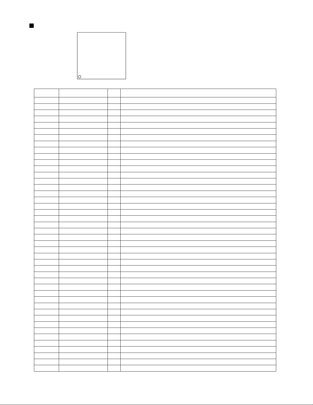
MN101C12GDW (IC851) : Panel micon
1.Pin layout
75
76
51~
50
MX-S6MD
2. Pin function
Pin No.
1
2
3
4~9
10
11
12
13
14
15
16
17~20
21
22
23
24
25
26
27~32
33
34,35
36
37~41
42
43
44
45~57
58
59
60
61,62
63
64
65~72
73
74~78
79~86
87~94
95
96
97
98
99
100
~
100
125~
Symbol
LEVEL Lch
LEVEL Rch
-
A / D Power
Vdd
8.38MHz
8.38MHz
GND
-
-
-
comm sysreq
LED STBY red
LED POWER green
-
-
comm panereq
-
comm reset
-
LED MD REC
-
comm out
comm in
comm clock
-
LCD WE
LCD RE
LCD CS1
-
LCD AO
LCD RESET
-
LCD LEDdimmer
-
LCD D7~D0
-
DVASS
-
LED RED
LED GREEN
LED BLUE
DAVdd
I/O
I
I
-
-
I
O
-
-
-
-
O
O
O
-
I
I
-
O
-
O
I
I
-
O
O
O
-
O
O
-
O
-
O
-
-
-
O
O
O
-
~
26
Function
Connect to ground.
Input terminal.
Input terminal.
Connect to ground.
A / D Ref. voltage.
Ref. voltage.
OSC frequency input terminal.
OSC frequency output terminal.
Connect to ground.
Connect to ground.
Non use.
Connect to ground.
System CPU require signal output terminal.
Stand by LED (RED) output terminal.
Power LED (GREEN) output terminal.
Connect to ground.
Connect to ground.
Panel CPU require signal input terminal.
Connect to ground.
Reset signal input terminal.
Connect to ground.
MD (RED) output terminal.
Connect to ground.
Commor signal output terminal.
Commor signal input terminal.
Commor clock signal input terminal.
Connect to ground.
Write enable output terminal.
Read enable output terminal.
Chip select output terminal.
Connect to ground.
Data select signal output terminal.
LCD reset signal output terminal.
Connect to ground.
Dimmer control terminal.
Connect to ground.
Pata bus signal output terminal.
Connect to ground.
Connect to ground.
Non use.
Red LED control terminal.
Green LED control terminar.
Blue LED control terminal.
Ref. voltage.
1-63
Page 64

MX-S6MD
NJM4580D (IC652) : LPF, Mic and H.phone Amp.
1.Terminal layout
2.Block diagram
+
V
INPUT
+
A OUT
A -IN
A +IN
V
1
2
A
3
-
4
(TOP VIEW)
B
8
7
6
5
+
V
B OUT
B -IN
B +IN
-
V
NJM4580E-W (IC672):
A OUT 1
A -IN 2
A +IN 3
V- 4
OUTPUT
8 V+
7 B OUT
6 B -IN
5 B +IN
1-64
Page 65

STK402-030 (IC301) :
1.Pin layout
115
2.Block diagram
4
R1
TR7
MX-S6MD
8
TR9
R13
TR4
R6
C1
1
TR1
2
TR3
R2
TR2
D1
SUB
R3
R4
R5
13
TR5
TR6
TR8
R7
1256710
TR10
11
R8
TR12
TR13
R9
TR11
R10
C2
R11
R12
TR14 TR15
TR16
R14
9
14
15
1-65
Page 66

MX-S6MD
TC74HC02AP (IC674) : 2ch Nor gate
1.Pin layout & block diagram
1
1Y
2
1A
3
1B
4
2Y
5
2A
6
2B
GND
7
14
13
12
11
10
9
8
VCC
4Y
4B
4A
3Y
3B
3A
2.The truth value table
TC7S08F-W (IC340) : Buffer
1. Pin layout 2. Block diagram
IN B
IN A
1
2
54VDD
A
A
L
L
H
H
B
L
H
L
H
Y
H
L
L
L
Vcc
Y
3
Vss
TC7S32F-X (IC603) : NAND gata
1.Pin layout
IN B 1
IN A 2
Vss 3
5 VDD
4 OUT X
OUT X
2.Block diagram
A
A
B
GND
Vcc
Y
GND
1-66
Page 67

TDA7439 (IC671) : Control volume
1.Pin layout
1
SDA
2
CRE
3
Vs
4
AGND
5
ROUT
6
LOUT
7
R-IN4
8
R-IN3
9
R-IN2
10
R-IN1
11
L-IN1
12
L-IN2
13
L-IN3
14
L-IN4
MUXOUTL
15
2.Block diagram
TDA7439
30
CSL
29
DIG GND
28
TREBLE(R)
27
TREBLE(L)
26
MIN(L)
25
MOUT(L)
24
BOUT(L)
23
BIN(L)
22
BOUT(R)
21
BIN(R)
20
MOUT(R)
19
MIN(R)
18
INR
17
MUXOUTR
16
INL
MX-S6MD
L-IN1
L-IN2
L-IN3
L-IN4
R-IN1
R-IN2
R-IN3
R-IN4
11
12
13
14
10
MIN(L)
26
MIDLE
25
MOT(L)
23
G
0/30dB
2dB STEP
INL
MUXOUT
15 16 27
VOLUME
2
I C BUS DECODER LATCHES
TREBLE
TREBLE(L)
9
G
VOLUME
TREBLE
MIDLE
8
7
INPUT
MULTIPLEXER
GAIN
17
18
201928
BIN(L)
24
BASS
BASS
2221
BOUT(L)
SPEAKER
AT T
LEFT
SPEAKER
AT T
RIGHT
SUPPLY
2
6
30
SCL
1
SDA
29
DIG-GND
5
ROUT
3
Vs
4
AGND
LOUT
INR
CREF
MUXOUT
MIN(R)
TREBLE(R)
BIN(R)
MOUT(R)
BOUT(R)
1-67
Page 68
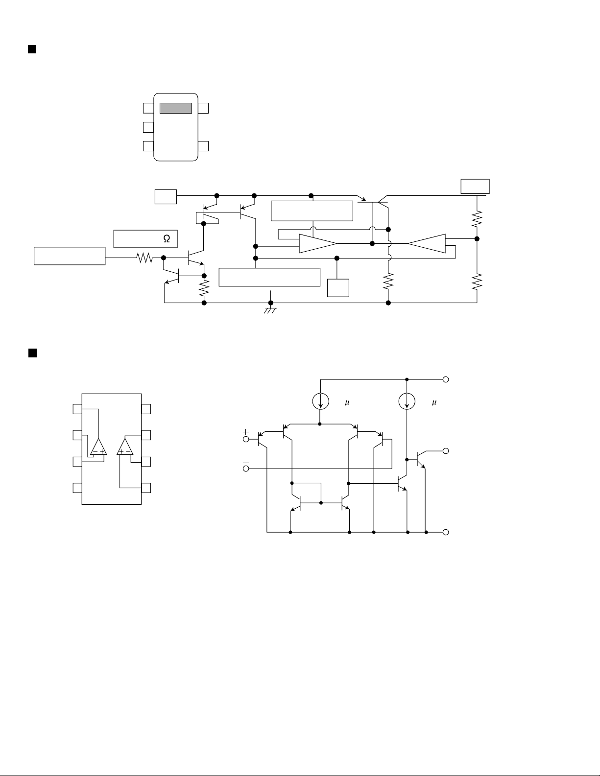
MX-S6MD
TK11140SC-W (IC485) :
1.Pin layout
on / off control 1
6 Vin
GND 2
Np (Vref) 3
4 Vout
2.Block diagram
VIN
Thermal Sensor
Rin=550k
on / off Ccont.
Bandgap Reference
GND
UPC393G2-W (IC602) :
1.Pin layout 2.Block diagram
VOUT
Cnp
V+
OUT1 1
Ii1 2
IN1 3
V- 4
12
8 V+
7 OUT2
6 Ii2
5 IN2
100 A 100 A
IN
Ii
Q1
Q2
Q5
Q3
Q4
OUT
Q8
Q7
Q6
V-
1-68
Page 69
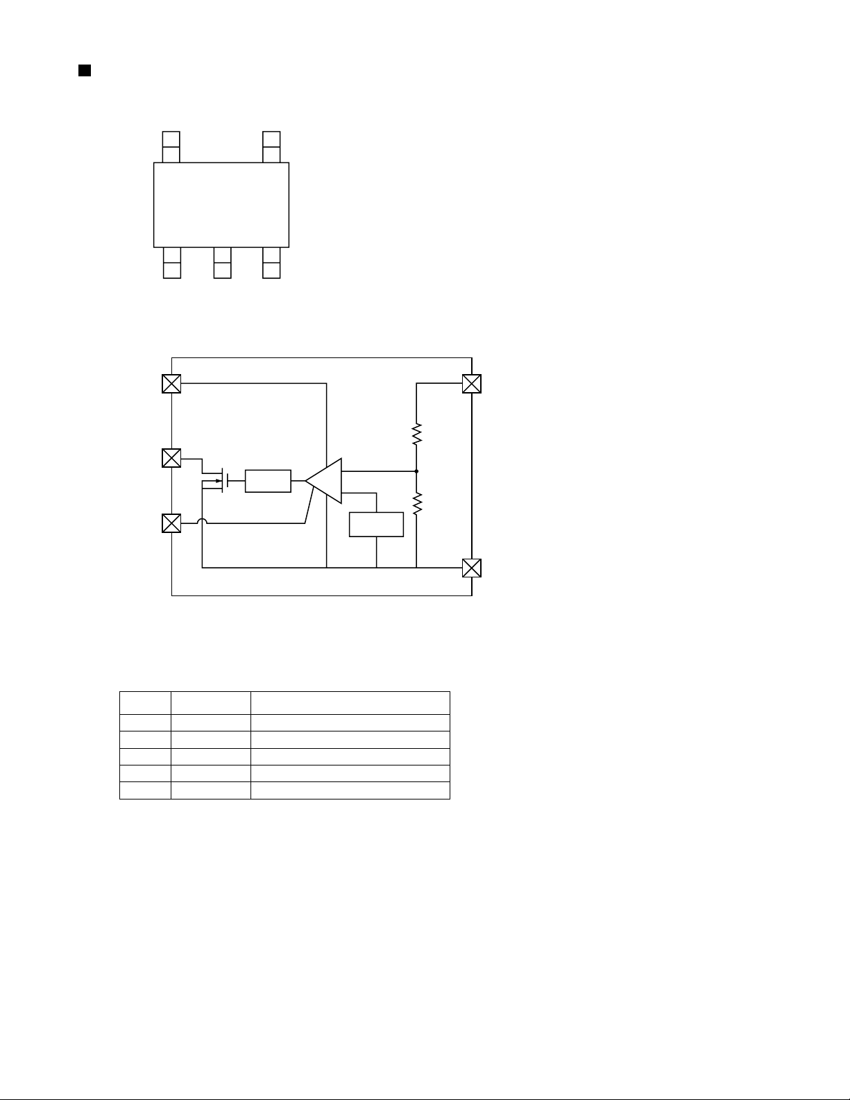
XC62ER3602M-X (IC400) :
1.Pin layout
54
MX-S6MD
1
2.Block diagram
V
DD
EXT
CE
3.Pin function
23
Current
Limit
+
-
Voltage
Reference
V
OUT
V
SS
Pin No. Symbol Function
SS
1
2
3
4
5
V
IN
V
OUT
V
EXT
CE
GND
Power supply input
Regulator output
Base current control terminal
Chip enable
1-69
Page 70

MX-S6MD
VICTOR COMPANY OF JAPAN, LIMITED
AUDIO & COMMUNICATION BUSINESS DIVISION
PERSONAL & MOBILE NETWORK BUSINESS UNIT. 10-1,1Chome,Ohwatari-machi,Maebashi-city,371-8543,Japan
No.20887
Printed in Japan
200011(O)
Page 71

MX-S6MD
Block diagram
CN321 CN408 CN407
MD PICKUP
KMS-260B
FEED MOTOR
6
5
SPINDLE MOTOR
Detection switch
SSTOP,MREF,MPROT
MAGNETIC
HEAD
LOADING
MOTOR
Detection SW
LOAD SW
PLAY SW
4
CN602
SW1~SW6
REST SW
FEED
M
3
SPINDLE
PICKUP
CN699
M
CN001
2
LINE IN LINE OUT
TAPEL
TAPER
TRECL
TRECR
1
I,J,A,B,C,D
FCS
TRK
FM
SM
LM
M
COM+
M
COM-
CN610
TRY1OPEN,TRY2OPEN,TRY3OPEN
TRY1CLOSE,TRY2CLOSE,TRY3CLOSE
CN601
T+,T-,F+,FFM+,FMSM+,SM-
CN923 CN922
MDL,MDR
MRECL
MRECR
SDA
SCL
FUNCTION
VOLUME
CD/MDL
CD/MDR
IC672
CD/MD LPF
KCMND,MSTAT
MRDY,KCLK,CDRESET
IC410
Power Driver
LOADSW,PLAYSW
AM+
ACT.MOTOR
AM-
DRIVER
CUM MOTOR
DRIVER
REST
A+C,B+D,E,F
MD,PD,LD
FOCUS/SPINDLE
FEED/TRACKING
IC671
IC310
RF AMP.
MPROT,MREF,SSTOP
LOAD
EJECT
IC851
IC852
RF & SERVO
IC801
BTL DRIVER
TLOUT
TROUT
CD/MD
IC673
CD/MD SEL
PEAK BOTM ABCD FE
AUX ADFG SE TE
SWDT SCLK XLAT
RF
XRST
IC500
Control Micon
SW690~SW693
COM_CCW,COM_CW
ACTM_CCW,ACTM_CW
EQSW
TBAL,FBAL
IC601
AMP
/RFDET,FE
BDO,TE
LDON,OFT
RFENV,ARF
TRD,KICK,FOD
ECM,ECS,TVD,TRV
CN602
AUXL
AUXR
IC674
CD/OPT IN SEL
MD
SUB_OP/CL
P.POSI1~P.POSI3
L,R
CD/OPT
TX
CDL
CDR
EMFO
IC450
Pre Driver
FRDR,FFDR
TRDR,TFDR
SFDR,SRDR
EMPHE
IC590
EEPROM
/RESET
STAT
/DMUTE
SUBQ
BLKCK
MLD
MDATA
MCLK
FLAG
IC651
CN691
CN661
IC350
Digital servo &
Encoder/Decoder
PWAD
PWDA
COMMAND
STATUS
CAMP1~CAMP4
IC251
UNIT MICON
CDTNO,CDCOPY,CDEMP
OUTL
OUTR
DSP
W601
LIN
POWER AMP
RIN
LRCK
SCLK
MCLK
SDIO
IC480
DA/AD converter
TXDO,RXDO,IC
E2SDL
E2SCK
RUNCLOCK,RUNDATA
RUNLOAD1,RUNLOAD2
KEY1,KEY2,SELECT
KCMND,MSTAT
MRDY,KCLK,MCS
IC652
OPE.AMP
SRDATA,LRCK,BCK
IC301
LSURR
MUTE
DIN
XWE
XRAS
XCAS
XOE
IC390
D-RAM
AOUT L/R
LIN/RIN
SW680
EEPROM
OUT_L
OUT_R
L
R
L,R
SPK
CN394
from CN304
RESET
IC201
J3001
CN521CN522
RESET
to Flash Micon to Running JIG
CN671
CN611 CN651 CN606
KEY SWITCH
S7101~S7106
TUNED,MPX,TCE,TCK
CN392 CN393
TDATA,MDSTAT,FCD
MDCMND,RSDA,RSCL
MDRESET,RESET
DAVN,MRDY,CDRESET
KCLK,MSTAT,KCMND
SAFETY1~3,FTU,INH,PRT
TRSW,POWER,SDA,SCL
STANDBY,AMUTE,SMUTE
W122
W121
CN912CN913
SW 12V
REG.
REMOCON
S7001~S7007
LS701
CONTROL
SYSTEM
CD/OPT,CD/MD,SURR
SPKR,TMUTE
TDATA,TCE
TCK,TUNED
MPX
DAVIN
RSDA
RSCL
TLOUT
TROUT
SW +10V/
+8V REG.
TUNER
+5.6V
TUNER
+9V
CN914
CN924
US DM
+6V REG.
IC701
JOY
IC801
MICON
AT101
ANT
MD A
+6V
JOYA+H
JOYB+G
JOYC+F
JOYD+E
JOYCOM1
JOYCOM2
JOYPUSH
VOLA
VOLB
TSU1~6
KEY1~3
REM
JOYA+H
JOYB+G
JOYC+F
JOYD+E
JOYCOM1
JOYCOM2
JOYPUSH
FM RF
AM
AMOSC
MRECL
MRECR
MDL
MDR
POWER
SUPPLY
US D
5.6V REG.
KEY2
KEY3
T111
REM
FMIN
L,R
SPK
MUTE
MDDIN
CN701
CN801
FMOSC
AMRF
CN301
CN911
W921
CN791 CN891
TSU1~6
VOLA
VOLB
KEY1
IC121
PLL
AMOSC
IC101
FMDET
/AMDET
CN304CN511
LSURR
POWER
SUPPLY
W301
CN991
T9002
SUB
TRANS
LCD
CN851
LSI,A0
LCDRST
WE,RE
DO~D7
IC851
PANEL
MICON
JS821
MASTER
VOLUME
S8101~S8106
CK,CE,DI/DO
LOUT,ROUT
FMOUT,STEREO
TUNED,MUTE
PROTECTOR
H.P.
SMUTE
MUTE
W3002
T9001
POWER
TRANS
IC191
RDS
PRT
W3002
RED
GREEN
BLUE
LCD
BACK LIGHT
FULL COLOR
LED
CN111CN112
CDRESET
MRDY
FCD
KCLK
KCMND
MSTAT
SDA,SCL
CD/OPT
AMUTE
CD/MD
J3101
L
H.P.
R
JACK
AUXL
AUXR
J3102
AUX IN
CN303CN302
CN692
MAINS
PLUG
BC
DE
F
G
HA
I
2-1
Page 72

Schematic diagrams
MX-S6MD
MX-S6MD
Powre supply section
2SC2785/FE/
C1304
R1309
2.7K
10/50
D1301
D2301
1SS133
1SS133
LVL-R
6
TDATA
TCE
TCK
TMUTE
TUNED
MPX
TLOUT
5
TROUT
W121
WJK0016-003A
FTU
LVL-L
2SC2785/FE/
2SC2785/FE/
47/25
C9606
Q9601
C9602
Q9602
C9605
47/25
47/25
C9601
D9601
C9604
0.01/16
D9602
MTZJ6.2C
0.01/16
MTZJ10C
R9601
47
R9602
1K
R9603
220
R9605 R9604
1K 2.7K
10K
R9606
4
CN913
QGB1214J1-14S
SDA
SCL
FCD
AMUTE
CD/MD
CD/OPT
CDRESET
KCLK
KCMND
MSTAT
MRDY
3
LVL-R
LVL-L
MDDIN
D9904
D9903D9902
1N4003
1N40031N4003
POWER
CN914
R1305
Q1301
4.7K
R1308
R2309
2.7K
Q9603
KRA107M
QGB2510J1-09
R1306
C2304
10/50
Q9604
KRC107M
6.2K
2SC2785/FE/
5.6K
CN924
QGB2510K2-09
6.2K
R2305
Q2301
4.7K
R2308
2SD1913/RS/
C9403
C9103
Q9401
47/25
47/16
C9401
D9102
R2306
MTZJ6.8C
QGF1016C1-21
C1302
10/50
C2302
10/50
5.6K
0.01/16
R9404
C9402
47/25
47/16
C9302
2SD2394/EF/
C9102
100/10
CN511
R9401
10
100
Q9301
2SD2394/EF/
MTZJ13B
D9301
Q9101
D9101
C2301
R2301
1.5KMTZJ6.8C
R9402D9401
C9301
0.01/25
R9305
MTZJ6.8B
100
R2303
10/25
2.2K
MRECR
R9301
4.7
470
R1303
R2302
12K 12K
C9101
100
C1301
R1302
R1301
KRA107M
0.01/25
220
R2304
10/25
2.2K
MRECL
Q9302
R9302
R9303
R9104
270
R9106
R9107
CN304
QGB2510J1-12
220
100
100
100
R1304
MDR
470
47K
MDL
1
1
R9101
MDDIN
270
R9306
R9410
1K
D9112
R9411
MDCMND
MDRESET
MTZJ7.5C
R9412
MDSTAT
R9901 R9902
68K
R9903 R9904
68K 18K
R9905 R9906
68K 36K
2SD2394/EF/
C9202
C9112
15K
Q9201
100/16
Q9111
2SD2394/EF/
100/10
D9201
D9111
MTZJ11B
C9111
MTZJ6.2C
0.01/25
R9114
C9201
R9116
SURR
STANDBY
R3014
47/25
C3005
2SC2785/FE/
Q3005
100K
PRT
D3002
SMUTE
10K
100K
R3012
R3013
KRC110M
10/50
2SA1175/FE/
Q3004
Q3003
10K
C3004
R3011
R1016
100K
R2016
82K
22K
2SC3576-JVC
R2103
Q2101
1.2K
R1103
1.2K
C3201
R2102R1102
1/50
R2101
680680
Q1101
R1101
2SC3576-JVC
KRA102M
22K
R3201
10K
10K
Q3201
MTZJ4.3B
R3016
C3010
C3011
D3001
R3038
C9901
100/10
QNZ0136-001Z
EP301
C3016
10/50
15K
0.22/50
100/10
MTZJ4.3B
10K
R9910
3.9K
C3302
2200/42
R3302
C3304
0.01/100
D3304
D3302
1N5402M-201N5402M-201N5402M-201N5402M-20
D3003
22K
MTZJ2.4B
47K
R3015
D3303
C3301
2200/42
R3301
D3301
C3303
0.01/100
WJK0015-004A
W301
SAFETY3
SAFETY2
SAFETY1
D9901
1
R9206
Q9203
KRA107M
0.01/25
R9205
220
1
R9112
270
1K
R9201
220
R9203
D9203
1SS133
10K
R9202
Q9204
KRC107M
270
1SS133
W302
D9910
1N4003
CN692
QGB1216K1-06S
R
L
W302
QUM025-15Z3Z3
AUXR
AUXL
C3103
0.1/50
R2201
R1201
C2101
TUNED
MPX
TCE
TCK
TDATA
MDSTAT
MDCMND
FCD
RSDA
RSCL
MDRESET
RESET
DAVN
MRDY
CDRESET
KCLK
MSTAT
KCMND
SAFETY3
SAFETY2
SAFETY1
FTU
INH
PRT
TRSW
POWER
SDA
SCL
CD/OPT
CD/MD
SURR
STANDBY
AMUTE
SMUTE
SPKR
TMUTE
1000P/50
C1101
QGB2510J1-04
220
220
1000P/50
CN301
CN302CN303
J3102
QNS0072-001
J3101
QNS0072-001
QGB1214J1-18S
QGB1214J1-18S
CN901
W901
QJK026-081803
W901
QJK026-081803
QGA2501F1-03
CN901
QGA2501F1-03
F9103
F9103
F9102
F9102
F9101
F9101
QNZ0079-001Z
TB991
TB992
QNZ0079-001Z
QNZ0079-001Z
TB991
TB992
QNZ0079-001Z
Parts are safety assurance parts.
When replacing those parts make
TROUT
TLOUT
MRECR
MRECL
MDR
2
1
MDL
+8V
CN912
QGB2510J1-14
INH
RESET
Q9503
KRC104M
D9504
C9502
R9504
1SS133
100K
4.7/50
R9503
Q9502
KRC107M
10K
Q9501
D9501
1SS133
R9502
KRC104M
6800/25
C9705
22K
R9703
C9704
D9708
C9708
0.01/50
10K
EP971
QNZ0136-001Z
D9503
2.2/50
C9501
MTZJ5.1C
D9707
D9706
R9801
22K
D9705
2200/35
C9805
C9804
D9704
D9804
D9703
1N40031N4003
1N40031N40031N40031N40031N40031N4003
0.1/50
0.1/50
C9701
D9801
C9801
D9803
D9802
D9702
D9701
0.068/50
0.068/50
1N4003
1N4003
1N4003
1N4003
C9709
R9701
D9709
1SS133
CN911
QGA2501C1-08
0.022/50
10K1SS133
10K
R9702
D9710
sure to use the specified one.
BC
DE
F
G
HA
I
2-2
Page 73

MX-S6MD
System control section
R7003R7004R7005R7006
R7002
R8032
R8031
R8030
R8029
R8028
R8027
R8026
R8025
R8024
2.2K
R8023
R8022
R8021
R8019
100
R8018
R8017
R8016
1K
R8015
2.2K
1000P/50
1K
S7002
C7012
0.001/50
100
100
100
100
100
100
1K
1K
1K
1K
1K
1K
100
C8004
R8020
1K
0.01/50
D8011
1SS355
R7001
S7001
1K
R8078
D8010
TDATA
10K
1SS355
1000P/50
1SS355
D8003
MDSTAT
MDCMD
FCD
C8018
RSDA
RSCL
MDRST
RESET
DAVN
TSU1
MRDY
REM
D8002
1SS355
R7020
1K
TSU6
TSU5
TSU4
TSU2
TSU3
JOYA+H
JOYB+G
JOYC+F
JOYD+E
JOYCOM1
JOYCOM2
JOYPUSH
KEY1
KEY2
KEY3
REM
VOLA
VOLB
REM
KEY2
CN801
CN701
QGB2011L1-14
QGF1210G1-23
CN791
QGB2011M4-14
QJB001-021602
W693
VOLA
VOLB
CN891
QGF1205F1-23
JOYA+H
JOYB+G
JOYC+F
JOYD+E
JOYCOM1
JOYCOM2
JOYPUSH
JOYA+H
JOYB+G
JOYC+F
JOYD+E
JOYCOM1
JOYCOM2
JOYPUSH
D8503D8504
QGF1005F2-28
REM
KEY2
KEY3
LED1
TSU3
TSU2
TSU4
TSU5
TSU6
TSU1
KEY1
KEY2
KEY3
REM
C8506
100/10
1SS3551SS355
D7
D6
D5
D4
D3
D2
D1
D0
RED
GREEN
BLUE
CN851
C8311
KEY1
0.022/50
100
100
100
100
100
100
100
100
R8526
R8527
R8528
CS1
R8518
R8519
R8520
R8521
R8522
R8523
R8524
R8525
LCDRSTA0WE
2.2K
2.2K
2.2K
R8101
1K
R8308
300K
C8304
4.7/10
4.7/10
4.7/10
C8301
C8302
C8303
300K
R8305
300K
R8306
4.7/10
1/161/161/161/161/16
C8305
100
R8310
C8111
0.001/50
10K
10K
C8211
0.001/50
1SS355
D8502
1SS355
D8501
R8103
1.2K
S8102
D7D6D5D4D3D2D1
2.2K
R8112
R8212
2.2K
R8111
R8211
C8510
QSW0651-001Z
QSW0651-001ZQSW0651-001ZQSW0651-001ZQSW0651-001ZQSW0651-001Z
S8103
100/10
D0
RE
R8102
1K
S8101
R8105R8104
2.2K1.5K
S8104
R8301 R8303
R8515
R8516
100
IC851
MN101C12GDW
C8501
R8501
1M
X8501
C8503
C8502
33P/50
R8106
2.7K
S8105
300K
R8307
C8306
C8307
C8308
C8309
360K 620K
220K
R8302
R8512
R8513
R8514
100
100
100
100
1.5/25
QAX0416-001Z
33P/50
S8106
R8203
100
R8503
TSU1
10K
2.2K
R8504
LED2
10K
2.2K
R8505
LED3
R8204
Q8602
R8602
MA3075/H/MA3075/H/MA3075/H/MA3075/H/
120
D8602
SLA-360MT
DTC114EKA
R8601
R8201
R8202
330
D8601
SLA-360LT
Q8601
DTC114EKA
2SC2412K/RS/
220
R8412
R8411
100
100
100
R8509
2.2K
100
R8507
1K
1K
Q8410
R8502
R8511
R8510
220
R8413
D8403
220
C8202
D8404
C8504
0.01/50
R8508
C8201
D8413
D8414
Q8411
2SC2412K/RS/
270
270
R8416
R8417
1K
0.01/50
JS821
QSW0862-001
0.01/50
D8401
NSTM515AS
1SS3551SS355
2SC2412K/RS/
270
R8419
1000P/50
C8505
TSU6
10K
R8506
TSU4
TSU3
TSU2
Q8412
R8420
LED1
TSU5
LED2
LED3
D8411
Q8416
2SC2412K/RS/
270
RED
R8444
1K
GREEN
R8445
1K
BLUE
R8446
1K
220
R8433
10K
R8447
R8434
C8401
220
R8435
2SC2412K/RS/
Q8419
10K
1/50
R8448
D8412
220
2SC2412K/RS/
Q8420
10K
1/50
R8449
C8402
D8417
D8418
Q8417
2SC2412K/RS/
270
270
R8438
R8439
2SC2412K/RS/
Q8421
1/50
C8403
D8409
NSTM515AS
1SS3551SS355
Q8418
2SC2412K/RS/
270
R8442
R8441
270
2.2K
R8450
R8451
2.2K
2.2K
R8452
R8453
2.2K
R8454
2.2K
R8455
2.2K
R7007
3.9K
220
KEY3
1K
2.2K
VOLA
R8048
R8004
1SS355
TRSW
R8047
1K
2.2K
R8005
2.2K1K1K
SAFETY1
D8007
D7001
SDA
POWER
R8045
R8046
2.2K
R8006
SAFETY2
D8008
R7010
SLR-342VC
SCL
R8044
2.2K
2.2K
R8007
1K
SAFETY3
1SS355
QSW0651-001ZQSW0651-001ZQSW0651-001ZQSW0651-001ZQSW0651-001Z
QSW0651-001Z
Q7001
DTC114EKA
QSW0828-001
LS701
SURR
CD/MD
CD/OPT
R8041
R8042
R8043
2.2K
2.2K
IC801
MN101C12GDX
C8001
1.5/25
R8008
1M
X8001
18P/50
33P/50
C8003
C8002
D8009
1SS355
S7007
AMUTE
SMUTE
STANDBY
R8038
R8039
R8040
2.2K
2.2K
2.2K
X8002
QAX0494-001Z
C8007
22P/50
SPK
R8037
2.2K
2.2K
QAX0401-001
22P/50
C8008
C8020
100/10
S7006
TMUTE
TUNED
R8077
R8036
2.2K
1K1K1K
R8011
R8012
MSTAT
KCMND
47
R8080
2.2K
C8021
1000/6.3
MPX
R8035
R8013
KCLK
2.2K
S7005
GP1U261X
IC701
TCE
R8034
R8014
CDRST
R7101R7102R7103R7104R7105R7106
6
S7106
S7105
S7104
QSW0651-001ZQSW0651-001ZQSW0651-001ZQSW0651-001ZQSW0651-001ZQSW0651-001Z
S7103
S7102
1K1K1.2K1.5K2.2K2.7K
S7101
5
0.01/50
C8030
C8031
0.01/50
0.01/50
C8005
0.01/50
C8006
PRT
4
22K
R8068
R8067
QGB1214K1-18S
CN392
TUNED
MPX
TCE
TCK
TDATA
MDSTAT
MDCMND
FCD
RSDA
RSCL
MDRESET
RESET
3
2
DAVN
MRDY
CDRESET
KCLK
MSTAT
KCMND
SAFETY3
SAFETY2
SAFETY1
FTU
INH
PRT
TRSW
POWER
SDA
SCL
CD/OPT
CD/MD
SURR
STANDBY
AMUTE
SMUTE
SPKR
TMUTE
22K
R8066
22K
R8065
22K
R8064
22K
INH
10K
220
10K
220
FTU
JOYA+H
JOYB+G
JOYC+F
JOYD+E
JOYCOM1
JOYCOM2
JOYPUSH
R8081
R8082
R8083
R8084
R8050
R8051
2.2K
1K
2.2K
BAND1
BAND0
47K
R8052
R8053
R8054
1K
R8055
1K
R8056
1K
R8057
1K
R8058
1K
R8059
1K
R8062
1K
R8060
10K
10K
R8063
R8070
R8071
R8072
Q8001
DTC114EKA
11K
10K
10K
R8090
47K
Q8002
DTA144EKA
R8001
KEY1
R8002
2.2K
KEY2
VOLB
R8049
R8003
2.2K
TCK
R8033
1K
1K
C8023
1K
100/10
R8094
1.2K1.5K2.2K2.7K
S7003
S7004
100/10
C7011
C8017
10K
CN391 CN393
QGB2510K2-04 QGB1214K1-18S
1
BC
DE
F
G
HA
I
2-3
Page 74

MX-S6MD
MX-S6MD
Function selector section
QGB1214K1-14S
CN923
6
CN602
QGB1216J1-06S
C6235
0.0022/50
C6135
0.0022/50
R6235
13K
R6135
13K
MDDIN
LVL-L
LVL-R
R6139
R6239
51K
51K
MRDY
MSTAT
KCMND
CDRESET
KCLK
TRECL
CD/OPT
MRECL
CD/MD
TAPEL
AMUTE
FCD
CD/MDL
SCL
TUL
TUR SDA
TAPER
CD/MDR
TROUT
TLOUT
MRECR
MRECL
MDR
MDL
QGB2510K2-14
CN922
SCL
SDA
TUL
R6133
TUR
6.8K
R6233
R6132
R6232
6.8K
CN691
QGA2501C1-03
L6141
2.7K
R6131R6231
4.7K4.7K
2.7K
C6141C6241
QQR0590-001
0.0056/500.0056/50
TLOUT
5
100/16
D6308
C6110
2.7K
C6310
C6114
C6214
R6329
220K
MTZJ11A
10/50
R6324
100
TDA7439
IC671
C6309
0.022/50
0.022
0.0056/500.0056/50
D6306
R6338
MTZJ5.1B
Q6308
1K
D6307
1SS133
KTA1273/Y/
Q6304
2SC2785/FE/
Q6305
R6311
1K
R6337
2SC2785/FE/
10K
L6241
QQR0590-001
10/50
10/50
10/50
10/50
10/50
C6101
2.2/50
C6205
C6103
C6210
R6206
C6104
C6211
2.7K
C6204
C6212
R6205
10/50
C6213
5.6K
C6203
C6112
R6105
C6201
C6113
5.6K
C6111
R6106
10/50
10/50
C6106
C6107
LVL-L
LVL-R
CN603
4
QGA2001F1-02
TRECR
MRECR
C6207
10/50
0.15/500.150.150.15
C6105
0.018/50
0.018
2.2/50
C6206
10/50
TROUT
FCD
W601
QJP001-031201
LIN
AGND
RIN
CD/MD
4.7/50
C2010
4.7/50
C1010
2SC3576-JVC
1SS133
D6310
R1019
R2019
1.5K
R1018
1.5K
R2018
1K
Q1002
1K
Q2002
R2017
2SC3576-JVC
R1017
27K27K
R1020
1K
2SK301/PQ/
Q3002
R3010
4.7M
220P/50
C1012
R2020
2.2/50
C1011
470P/50
1K
C3017
56K
R1031
1M 0.47/50
R3009
R3008
1.2K
IC301
STK402-030
C1020
3.3P/50
47/50
C1022
100P/50
R1030
CD/OPT
R1009
C1007
C1021
750
56K
Q3010
KRA104M
C3012
100/35
C2012
470P/50
2.2/50
10K
C2011
KRC104M
Q3011
R3037
R3035
100
C3013
10/50
C3014
10/50
R2009
56K
3.3P/50
C2007
Q3012
KRC102M
R3036
100
C3015
100/35
R3040
R1006
0.33
220P/50
C2020
C2021
47/50
R2031
R2030
100
56K
750
C2022
100P/50
R1014R2014 R1013R2013
D1001
D2001
R1010
4.7
QQLZ005-R45
0.33
L1001
R1007
Q1001
18K18K 1K1K
KTA1268/GL/
1SS133
47K 47K
R2015 R1015
1SS133
KTA1268/GL/
Q2001
L2001
R2006
0.33 QQLZ005-R45
R2007
4.7
0.33
R2010
R3001
100
R1011
C1008
C2008
R2011
4.7
0.1/500.1/50
4.7
RY301
QSK0057-001
C3001
R3005
1.5K
1/50
R3004
100K
R1003
Q3001
KTD863/Y/
R2003
4.7
4.7
0.022/50
C1001
0.022/50
C2001
C1002
0.01/50
0.1/50
C1003
0.1/50
C2003
C2002
0.01/50
QNB0010-001
J3001
KRA104M
470
R6306
3
2
150P/50
150P/50
J6301
J6301
QNN0365-001
QNN0173-001
AMUTE
R6108
C6123
C6223
R6208
27K
27K27K
R6107R6207
27K
2SC3576-JVC2SC3576-JVC
R6110
R6109
3.9K
Q6320
R6128
R6127
R6227
Q6301
Q6302
18K 18K
R6210
1K
1K
2.2K
R6228
2.2K
R6209
3.9K
KRC107M
KRA104M
Q6321
TAPEL
TAPER
TRECL
TRECR
CD/MDL
CD/MDR
22/50
C6115
22/50
C6215
R6125
11K
C6117
C6118
0.0047/50
C6116
R6111
C6119
0.1/50
0.1/50
2.2K
C6219
1000P/50
1000P/50
C6217
C6218
R6211
NJM4580D
IC672
0.1/50
0.1/50
C6216
2.2K
R6112
R6225
11K
0.0047/50
R6212
270
R6305
R6114
100K
R6214
100K
100/10
R6304
0.022/50
47/25
C6306
C6305
10K 10K
C6304
2.2K
2.2K
R6303
CN661
QGF1016F3-19
R6340
100
R6341
100
R6342
100
R6343
100
R6344
TX
100
100
R6345
R6118
CDL
C6307
220
22/50
R6218
CDR
IC673
TC4066BP/N/
220
Q6307
Q6306
47K
47K
R6307
MDL
MDR
R6327
C6308
Q6303
KRC104M
1
4.7/50
KRC104M
TC74HC02AP
IC674
R6334
TX
1SS133
D6309
D6311
47/25
C6311
1.5/25
R6333
MDDIN
C6314
100
J6310
GP1FA550RZ
R6332
L6801
100 1SS133
QQL231K-4R7Y
C6315
47/25
100
QGB2510K2-12
CN394
Parts are safety assurance parts.
When replacing those parts make
sure to use the specified one.
BC
DE
2-4
F
G
HA
I
Page 75

CD servo control section
MX-S6MD
TP3
QSW0865-001
SW680
SW690
SW690
SW691
SW692
6
SW693
SW1
SW2
SW3
SW4
SW5
SW6
5
SW691
SW692
SW693
QGB1214K1-08S
QSW0886-002
QSW0886-002
QSW0886-002
QSW0886-002
CN620
4
0.1
C003 C002
HDU-110
0.1
1
C001
CN001
VR001
1k
3
CN699
EMV7169-006R
VSH1173-001
PPN-13KA10C
QAR0123-001
2
1
TP7
TP6
TP5
TP4
TP8
TP9
QGB1214J1-08S
CN610
FF+
T+
T-
FM+
FMSMSM+
CN601
QGF1016C1-21
TP10
22k
R263
RF-500TB-12560
R861
R862
R863
R864
R866
R865
22k
22k
R262
R261
47k
47k
R636
R887
R886
R885
R884
TP11
RF-500TB-12560
1k
330k
1k
330k
1k
330k
A+C
F
R608
E
R607
B+D
91
M851
M852
1k
1k
1k
1k
SUB_OP/CL
TRY1OPEN
TRY1CLOSE
TRY2OPEN
TRY2CLOSE
TRY3OPEN
TRY3CLOSE
F
E
B+D
A+C
P.POSI1
P.POSI2
P.POSI3
CAMP1
CAMP2
CAMP3
CAMP4
SW690
SW691
SW692
SW693
L853
10
AM+
C859
1/16
AM-
L854
10
CM+
C860
1/16
CM-
C602C601
0.0010.001
C633
0.022
IC601
AN8849SB-W
10
R635
120
2SA1037AK/RS/-X
Q631
LA6541-X
IC801
C624
100/10
R631
2.2
C631
10/16
R811
C632
1/16
R632
R634
12
LB1641
IC851
R852R851
AM-
ACTU_CW
ACTU_CCW
47k
R606
R605
33k
68k
C607
0.1
R603
C604
0.022
C603
0.022
1/16
C623
C608
C619
33p
T+
390p
C814
47k
390p
C812
SM- T-
SM+
0.027
1/16
1/50
C614
C611
C612
4p
R613R611
750750
2.2k
R617
C802
F+
F-
470p
R813
1.2k
C816
C801
0.015
390p
2.2/10
2.7k
R801
C811
390p
C813
FM-
FM+
IC852
LB1641
SUBQ
CDTNO
CDCOPY
CDEMP
1k
1k
100
CAMP1
R285
R284
R283
10k
R287
10k
R288
10k
C852
0.01
0
NI
10/16
C851
AM+
CM+
R601
680k
R602
180k
C642
R641
270p
150k
0.0022
C641
0.022
C605
C606
220p
R604
220k
0.0027
820p
330p
C617
C616
C615
0
R614
R612
16k
1/10
C610
16k
C613
R812
3.3k
C815
1/10
R803
R804
R802
R808
R807
R805
R806
0.056/25
R647
9.1k
220k
3.9k
C821 C822
1/16 220/10
27k
R809
1.2k
1.2k
8.2k
27k
C853
0.01
NI
R854
UDZS5.6B-X
D852
CAM_CCW
CAM_CW
TBAL
FBAL
FE
390k
R642
TE
LDON
C625
C626
C621
NI
0.1/16
/RFDET
OFT
TP1
BDO
RFENV
ARF
TRD
KICK
FOD
ECM
ECS
TVD
TRV
0.1/25
C855
CM-
GCTRL
100/10
0.1/25
C622
TP2
EQSW
CAMP2
TRY3CLOSE
TRY3OPEN
TRY2CLOSE
TRY2OPEN
TRY1OPEN
TRV
TVD
ECM
ECS
KICK
TRD
FOD
FBAL
TBAL
FE
TE
RFENV
OFT
/RFDET
BDO
LDON
R659
1k
MA152WA-X
68k
C643
R643
0.1/16
R645 R644
2.2k 2.2k
R646
68k
C644
0.1/25
TC7S32F-X
IC602
IC603
SQCK
IC602
UPC393G2-W
R257
KCMND
MSTAT
KCLK
RXDO
TXDO
22k
22k
22k
1/16
1/16
C272
C271
R271
R272
R274
R682
1k
C676
0.1/25
R661
1k
R683
1M
R667
4.7
D667
R648
IC603
R289
1k
1k
R259
KEY1
KEY2
6.8k
6.8k
R276
R277
1/16
C270
STAT
/RESET
/DMUTE
1k
1k
R651
R652
470p
C661
ARF
68k
0.1/25
100/10
C679
10k
10k
R649
R662
NI
C680
R672
0.022
0.022
C663
C664
OUTL
24k
R695R696
24k
OUTR
10k
UPD780024AGKB08
X251
TRY1CLOSE
NAX0397-001X
MLD
SUBQ
SQCK
BLKCK
1k
1k
R654
R653
C653
0.33/16
IC651
MN662748RPM
680k
68k
R685
R671
DTA114EE-X
120k
330
R664
Q673
R663
NI
C666
120k
R673
1.5M
D673
DA204U-X
0.15/16
C665
R668
10k
R691
R701
C693
0.0068
C694
0.0068
R702
10k
R692
R293
IC251
MCLK
MDATA
820
NJM4580E-W
R705
4.7k
NJM4580E-W
P.POSI1
SUB_OP/CL
K655
C667
R703
IC652
IC652
820
R704
P.POSI3
P.POSI2
BLKCK
NQR0007-002X
5.6k
R669
0.47/16
10k
C691
R706 R707
10k
MCS
MRDY
1k
R256
1k1k1k
R278
R279
R280
CAM_CW
CAM_CCW
ACTU_CCW
SRDATA
LRCK
BCLK
K656
K657
K658
150
R665
QAX0599-001Z
C651
8p
390p
C695
2k 6.8k
390p
C692
10k
1k
0
R281
R294
ACTU_CW
NQR0251-004X
NQR0251-004X
NQR0251-004X
X651
C652
8p
0.047
C696
R201
RUNCLOCK
RUNLOAD1
RUNLOAD2
RUNDATA
SELECT
CAMP4
CAMP3
EQSW
GCTRL
C657
C655
220/10
0.1/16
OUTR
OUTL
0.1/25
220/10
C673
C677
0.1/25
C669
C656
220/10
R710
220
C699
220/10
100
R708
10/16
100
R709
0.1/25
C250
BR24C01AFV-W-X
IC201
TXDO
RXDO
R282
10k
1k
MCLK
R251
1k
MDATA
R252
1k
MLD
R253
1k
/DMUTE
R254
STAT
/RESET
47/6.3
0.1/25
C254
C253
220
R666
R670
100
OUT_L
OUT_R
R291
1.2k
R292
1SS355-X
10k
KCMND
MSTAT
MRDY
KCLK
MCS
OUT_L
OUT_R
CDEMP
CDCOPY
CDTNO
BCLK
LRCK
SRDATA
Q291
2SB1424/QR/-X
KEY1
KEY2
SELECT
RUNCLOCK
RUNDATA
RUNLOAD1
RUNLOAD2
R258
R260
R255
R286
C658
0.1/25
D291
C291
47/16
NI
CN671
QGF1016F3-08
CN611
1k
1k
1k
1k
CN651
QGF1016F3-19
CN606
QGF1016F3-07
CD PLAYBACK SIGNAL
BC
DE
F
G
HA
I
2-5
Page 76

MX-S6MD
MX-S6MD
MD servo control section
C323
C326
XLRF
R314
13k
R313
100k
C341C340
0.0220.022
C403
R436
22k
R438
22k0.01
R432C433
12k
R434
12k
AK93C65AF-X
0.0068
R328
0.22
100
0.022
C324
R315
24k
R342R341
2.2k2.2k
R300
R440
10k
10k
R441
Q410
DTC114EKA-X
Q411
DTC114EKA-X
C316
0
EJECT
SPRD
SPFD
LOAD
SFDR
SRDR
1
C317
IC340
TC7S08F-W
C342
0.1
SVIB
4REC
0.1
C591
R591
NI
100k
R592
SPFD
SPRD
SFDR
SRDR
FRDR
FFDR
TFDR
TRDRA11
R389
330
47/4
0
R559
MNT1
SET3
DIN1
1k1k1k
R558
R557
MNT0
10k
10k
10k
10k
1k
R563
CAM4
1k1k1k
R394
R393
LRCK
DADT
SET1
MODESE
R556
R555
1k1k1k
R564
R565
CAM3
CAM1
R392
XBCK
1k
R554
R553
R552
R551
R566
CAM2
C355
0.1
560
R391
FS256
A03
100k
NI
100k
100k
R522
R531
R532
R533
C351
C378
33p
IC350
CXD2662R
A02
A01
A00
A10
A04
A05
A06
A07
A08
1
XINT
DQSY
SQSY
0.1
C512
R506
2.2k
10k
10k
10k
1k1k1k
R567
R568
R569
MPROT
SSTOP
HREF
PEAK
10k
10k
100k
C361
R370
330
R397
DIN0
SVIB
R361
R362
R363
R364
R365
R366
R356
R367
R368
R369
330
R398
DIN1
0
R548
R511
1k
1k
1k
1k
1k
1k
1k
1k
1k
1k
330
330
330
R396
R399
R390
LRCKI
DATAI
DOUT
R549
NI
0
0
R546
R547
IC500
HD6432345A13FA
1k
R513
XRST
330
R387
XBCKI
R545
SENS
0.1
10
0
1k
R514
XLAT
L351
R562
ADDT
R561
MNT3
R534
R535
R536
R537
C350
000
R560
MNT2
R372
K346
NQR0360-001X
NAX0355-001X
C373
C358
R355R354
10k10k
0.1
R371
C372
NI
D351
NI
NI
C374
NI
C371
NI
D350
NI
R335
47k
R334
47k
R333
47k
R332
47k
R339
47k
LOAD
4REC
EJECT
1k1k1k
R510
R512
XTSLTXRECP
BOTM
330
R324
R323
0.0068
EDO
EDI
ESCL
ECS
C322
ABCD
330
FE
1k
AUX
TP331
330
1
R322
330
1
330
C329
NI
4.7k
R325
C319
TP332
EDO
EDI
ESCL
ECS
0.033
SE
TE
R343
1k
R317
10k
STSRDY
STATUS
COMMAND
COMCLK
MODON
MODCHG
F0CNT
APCREF
SWDT
R518
SRDT
R519
SCLK
PWAD
PWDA
EMPHA
ADFG
100k
R326
C321
0.0047
C320
R321
R320
56k
C328
0.1
R316
100k
C318
10k
R593
0
MNT0
MNT1
MNT2
MNT3
SWDT
SCLK
XLAT
SRDT
SENS
XRST
SQSY
DQSY
RECP
XINT
TX
XRST
XTSL
X350
0.1
K353
VREF
K505
NQR0389-003X
C510
C515
0.1
R521
R517
R509
100k
R515
R516
1k
1k
R520
R523
1k
1k
R524
1k
R525
NQR0389-003X
C359
NI
1k
1k
1k
1k
C325
0.01
C312
C310
0.001
47/4
C327
0.1
6
C311
1
QGF0501F2-21X
CN321
R305
2.2k
MODCHG
8.2
R330
27
R331
2SA1363/EF/-X
Q400
R306
470k
Q330
2SA1362/G/-X
R338R337
C331
NI
C330
0.1
C302
0.1
R302
5
FCS+
FCSTRK+
TRK-
C300
C301
R301
C303
NI
0
DTA113ZKA-X
TP305
0.1
NI
0
Q333
Q332
DTA113ZKA-X
MODON
4
C402
47/16
1
R420
FRDR
R421
22k
10k
C421
R422
FFDR
3
QAR0144-001
MT603
CN407
CN611
QGF1016F3-08
QGF1006F2-08W
100p
CN451 CN408
QGF1016F2-04W QGF1006F2-09W
CN612
QGA1501F1-02
S611
2
1
QSW0848-001
QAR0144-001
FF-110PH-08280
NSW0057-001X
S601
S602
S602
NSW0007-001X
QAH0039-001
CN601
QGF1006F2-09W
MT601
MT602
H601
TFDR
VREF
NI
C405
C406
C408
C407
100p
NI
0.01
NI
C416
C415
TP422
C455
CAM4
CAM3
CAM2
CAM1
SM+
SMFM+
FM-
MPROT
HREF
SSTOP
100p/100
22k
R424
R426
560p
R423
10k
C423
560p
560p
C425
22k
R425
10k
R427
10k
22k
C427
560p
C412
0.1
LM-
LM+
0.1
C453
R455
22k
R454
1
R453
1
22/16
C410
C400
C411
FCS+ SMFCS-
TRK+
TRK-
100/16
C450
IC410
IC450
BD7910FV-X
4.71
C334
0.1
330p
R401
M63008FP-X
15k
R402
R309
470k
0.0022
C314
C307
0.022
R310
330
100k
0.15
C333
R336
100/6.3
C401
5.6k
SC802-06-X
SC802-06-X
Q331
DTA114EKA-X
LM+
LM-TRDR
R451
47k
R452
NAD0006-103X
56k
D451
D452
R311
SM+
FM+
FM-
C452
1SS355-X
R340
2.2k
R456
D310
18k
C315
0.001
XC62GR3712M-X
TP441
0.1
C451
D454
NI
D453
NI
NI
Q451
R429
C431
0.0039
100/4
3.9k
IC400
C439
C429
R437
C435
C404
3.9k
R431
0.0056
0.01
R435
1000/6.3
0.0039
R428
15k
R430
15k
3k
8.2k
CXA2523AR
DTRF
CKRF
C437
3k
R439
R433
8.2k
0.0056
R312
IC310
10k
47/4
IC590
DTRF
APCREF
XOE
XCAS
47k
47k
47k
R540
R541
R538
R529
R528
NAX0361-002X
NI
R501
R502
3.3k
TP535
47k
ADFG
XLRF
CKRF
F0CNT
XRAS
A09D1XWED3D0
R530
NI
CDTNO
CDCOPY
NI
CDEMP
NI
C501
18p
X500
C502
18p
C511
0.1
R503
10k
R504
33k
D2
0.0022
0.0022
C480
C481
C484
C485
C486
C488
PWAD
PWDA
FS256
LRCK
XBCK
ADDT
DADT
EMPHA
DTA113ZKA-X
DTA114EKA-X
R375 R376
10k 100k
C492
C491
47/6.3
1
10/16
0.1
0.1
10/16
C353
1
AUX
ABCD
BOTM
PEAK
C375
TE
SE
1
FE
C354
R395
1k
C352
R378 R379
3.3k 1k
C376
0.01
R490
NI
R381
R380
47/4
R382
1k
470p
0.47
C380
150
0.015
1M
C379
C377
R377
680k
R492
470
R491
470
IC480
AK4519VF-X
DTC114EKA-X
C391
NI
IC390
HY51V17400CT-60
D0
D1
XWE
0.47
XRAS
A11
A10
A00
A01
10
A02
L352
A03
C390
10
0.01
C493
C490
1
IC485
TK11140SC-W
C497
0.1
C496
1
R497
R483
R481
C487
22/6.3
C483
0
4.7/35
C482
0.1
10
C489
1
C495
NI
R496
0.1
470
R495
470
NQR0022-005X
NQR0022-005X
NQR0389-003X
K524
C494
NI
K496
NQR0022-005X
NQR0022-005X
L525
NQL274M-1R5X
K492
K491
K495
L526
NQL274M-1R5X
K523
XCAS
XOE
A09
A08
A07
A06
A05
A04
DATAI
LRCKI
XBCKI
CDTNO
CDCOPY
CDEMP
K521
K522
NQR0354-001X
NQR0354-001X
NQR0389-003X
DOUT
DIN0
D3
D2
NINININININI
COMMAND
100p
C590
K527
K528
K529
K530
K531
K532
RESET
STATUS
COMCLK
STSRDY
SET3
DIN1
SET1
MODESE
NI
CN522
CN521
QGF1006F2-21W
MD PLAYBACK ANALOG SIGNAL
MD PLAYBACK DIGITAL SIGNAL
MD RECORDING ANALOG SIGNAL
MD RECORDING DIGITAL SIGNAL
BC
DE
2-6
F
G
HA
I
Page 77
MX-S6MD
Printed circuit boards
R1015
R6337
C6335
R2030
K6304
R6329
R6137
K6332
R3041
R1006
R1003
Q1001
C2022
C2021
K6305
C1002
R6237
K6337
C6309
C6214
Q3012
R1009
C1021
R2031
C2007
CN922
C1007
R1031
C2002
C6114
R3036
R6106
C1022
C6318
C2020
R2009
IC301
R1030
C1020
C6110
C3017
C6111
L6141
R6105
K6334
J3001
C6112
C6113
C6212
C6141
R6205
L6241
C6211
C6213
C6105
C6205
C6210
C6241
IC671
R6206
R6131
R6231
R6233
R6133
R6132
R6232
C6202
D9501
C6102
CN303
CN302
Q9503
C9504
EP971
CN301
D9710
D9503
C9706
C9501
D9709
R9902
R9701
R9702
C9502
R9503
R9502
Q9502
Q9501
D9504
R9504
R9901
C9708
R9904
D9910
R9401
R9903
R9703
C9703
C9709
C9704
R9402
D9402
D9706
C9807
W912
D9708
D9705
C9806
CN911
D9707
C9401
C9802
R9403
C9801
C9702
C9701
D9401
D9802
D9801
C6206
R9404
D9701
C6107
C6104
C6207
C9402
D9704
R6109
D9703
Q9401
D9702
R6209
C6106
D6311
C9707
D9803
R6325
C9403
D9804
Q6320
C9803
C6204
C6101
Q6321
R6228
R9410
C6201
L6801
C9804
R6107
R6128
R9412
R6326
R9801
Q6302
R6207
R6210
Q6301
R6332
D9902
D9903
D9905
R6208
R6108
R6227
R6110
R9411
C9705
C6221
Main board
R3008
R3040
6
R1019 R1020
C1010
C1012
R1017
Q1002
R3001
C6124
K6319
C6118
R6125
R6334
Q2002
R2019
C6117
R2017
R3035
C3012
C6135
C6307
C6217
C1005
C2005
R6211
R6327
R2020
C6218
R6225
IC672
C6235
C3014
R6307
C6225
C6224
C2012
R6112
C6219
R6214
C6115
CN913
R1018
R2018
W601
R3010
R6333
K6315
CN602
D6310
C3020
IC674
Q6306
Q6303
C2010
Q3011
IC673
C6308
R6114
R6303
Q3010
C3013
CN603
R6111
C6119
C6116
C6125
C6304
K6340
5
4
3
2
C6311
C6216
R3004
CN394
R6306
C6215
C1011
C2011
K6318
Q6307
C6306
R2015
R3005
K6317
K6320
R6304
R3009
C3001
C6314
Q3001
R6343
R6135
D6309
R6212
R6305
R6139
R6345
C6305
R6239
Q3002
Q2001
RY301
R2006
R2010
C2008
R2011
C6317
W602
R6342
C6203
R6235
C6103
L2001
R2007
R6218
R6311
R6118
R2013
R2014
D2001
R6344
R6336
D6308
R6340
R6341
D1001
C1008
K6339
C3040
R3037
R1010
K6303
Q6304
C6336
R6324
C6310
CN691
R6138
R6238
K6338
R6338
K6336
Q6308
R6236
R6136
L1001
D6307
R1011
C2001
K6306
D6306
Q6305
R1013
K6335
C3019
C3015
R3042
R1007
R1014
C1001
R2003
CN661
K6307
K6333
1
C9805
C6316
J3101
C6223
C6123
C6121
R6127
K6314
D9904
J3102
R9905
J6301
J6310
R9906
CN511
C2101
C2201
C3103
C9412
K9405
K9403
C1201
K3101
C1101
K9404
L2101
L1101
R9420
K9406
C9411
C3101
Q3005
R1201
R2016
R1016
R3014
K9402
R3103
C3102
C3005
R2201
C3016
CN914
Q3004
Q3003
W302
D3002
R3013
R3012
R3015
R3016
D3001
C3010
CN692
R3011
W301
R3101
R3102
R1105
D3003
C3011
R1104
C3201
R9910
C9901
C3004
Q1101
Q1102
R1102
K9401
R1103
W302
Q2102
R3201
Q3201
R1101
D9901
R2104
R2304
R2101
R2307
R1303
R2303
Q2101
R2103
R2105
R1307
C2302
R9607
R2102
R3038
R1308
R2308
Q2301
Q9604
R9601
C1303
R9602
R1304
R2305
R9604
C2303
R1305
Q1301
C1302
D9601
R9606
C9605
D9602
R9603
CN304
Q9603
R2306
R1306
C1301
C9604
R3301
C3306
C9602
C9601
Q9601
R3302
C2301
C2304
R1309
C9603
Q9602
C3304
C3303
W122
R9605
R2301
R2309
R2302
K9601
C3301
C3302
R1301
R1302
C9606
D2301
C9607
C1304
CN912
W121
D3304
D3302
D3303
D3301
CN913
D1301
EP301
BC
DE
F
G
HA
I
2-7
Page 78
Micon board
MX-S6MD
MX-S6MD
D8502
L8501
D8501
CN891
C8506
6
D8411
D8418
D8409
R8601
R8602
5
4
S8105
R8106
Q8601
S8106
R8411
R8412
R8105
R8413
D8405
D8401
R8414
Q8602
R8415
R8416
D8414
D8601
R8417
R8418
D8602
D8403
R8419
D8413
R8420
K8502
D8412
L8502
D8402
T9001
L8301
Q8410
D8404
R8310
D8503
D8504
D8417
D8410
D8406
D8407
D8408
Q8411
C8504
K8301
C8505
R8511
R8502
IC851
R8307
C8302
C8305
B3003
C8307
C8304
C8303
RY901
CN851
C8301
D8415D8416
Q8413
Q8412
Q8414
Q8415
Q8416
C9001
R8308
B3005
C8309
C8306
Q8417
R8305
T9002
C8308
R8306
Q8418
TB902
TB901
R8514
R8515
R8304
R8516
R8512
C8311
R8513
R8202
R8201
R8421
R8422
R8423
R8424
FT991
FT992
R8425
R8510
R8426
R8508
R8509
R8506
R8507
R8518 R8519
JS821
C8201
C8202
R8427
R8428
R8429
R8430
R8431
R8505
R8432
R8504
R8433
R8503
R8434
K8501
R8520
R8303
R8435
C8503
C8502
R8436
X8501
R8437
R8302
R8438
C8501
R8439
C8510
R8501
R8440
R8441
R8521
R8442
R8522
R8301
R8443
R8212
R8527
R8525
R8451
W693
R8111
R8450
R8444
Q8419
R8526
R8447
R8445
Q8420
R8523
R8524
C8401
R8452
R8203
R8204
R8528
R8453
B3004
C8212
C8402
R8112
C8404
R8449
C8403
R8446
R8211
R8111
C8211
S8101
Q8421
R8454
C8405
R8455
CN791
R8101
R8102
S8102
S8103
R8104
R8103
S8104
R8448
D8002
D8003
D8010
D8011
L8001
R8094
K8002
L8002
K8003
R8033
R8034
R8035
R8036
R8077
R8020
R8027
R8028
R8029
R8030
R8032
K8004
R8031
R8037
K8001
C8025
R8038
R8039
R8078
R8040
K8005
R8041
R8042
R8080
R8026
R8043
R8044
R8013 R8014
R8021
R8022
R8023
R8024
R8025
R8045
R8046
R8047
R8048
R8049
C8018
C8023
R8019
C8024C8030
R8016
R8018
C8031
R8017
C8021
R8015
C8004
R8050
C8005
R8011
R8051
C8006
R8012
R8075
R8081
C8020
IC801
R8082
C8017
R8083
R8084
C8002
R8008
X8002
C8003
C8001
R8053
X8001
R8064
C8008
C8007
R8052
R8004
R8003
R8002
R8001
R8007
R8006
R8005
Q8001
R8072
R8071
R8070
D8009
D8008
D8007
R8054
R8068
R8090
R8055
R8067
Q8002
R8056
R8066
R8063
R8060
R8062
R8059
R8058
R8057
R8065
CN801
CN391
CN392
Q9204
CN924
D9203
R9103
R9203
C9103
D9102
C9102
D9101
C9203
D9202
C9202
D9201
Q9203
C9113
C9112
D9112
D9111
R9114
R9104
R9306
R9201
R9101
R9202
Q9302
R9113
R9117
R9116
R9112
R9205
C9303
R9301
R9207
R9106
R9107
D9005
R9008
C9003
D9004
Q9003
R9004
R9007
R9009
C9004
W901
D9003
W921
C9002
D9006
Q9006
Q9004
R9005
Q9005
3
D9001
FT922
CN991
FT911
FT912 FT921
2
S7001
S7102
Q7001
R7002
R7001
R7020
1
CN701
S7002
LS701
R7003
S7003
R7102
R7101
S7101
S7103
R7103
R7104 R7105
S7104
S7105
R7106
S7106
R7007
S7007
D7001
R7004
S7005
S7006
S7004
IC701
C7012
C7011
R7010
R7005 R7006
D9302
D9301
R9303
R9302
R9305
R9206
C9302
C9111
C9301
C9201
C9101
CN393
Q9301
Q9111
Q9201
Q9101
BC
DE
2-8
F
G
HA
I
Page 79
MX-S6MD
MD servo board
(Forward side) (Reverce side)
S602
6
MT602
MT601
S601
CN601
5
L525L526
K491
C491C492
R490
R523
R342
R338
Q332
C312
K492
R519
R515
R518
R524
C342
R341
C340
R337
R330
C329
C334
C302
C341
R331
C590
R395
Q333
C330
C480
Q331
C331
C311
R325
C485
C486
C482
IC480
Q330
C317
C316
R483
C481
R311
C315
IC340
C322
C487
R481
C483
C320
C495
C494
R496
R495
D310
R300
R312
K495
K496
R529
R530
C501C502
R535
R514
R536
R528
R538
R534
R537
R430
R428
R420
R422
C411
R364
C410
R565R566
R563
CN407
C429C431
R429
R431
R564
C406
R389
C415
R504
R503
C511
R506
R569
CN408
C408
C407
C405
R362R363
R361
C416
R568
R455
C453
C450
C435
R435
R434
IC450
R522
R451
R452
R426
R456
Q411
R424
R432
Q410
R441
C352
Q451
C433
R433
R439
R440
C452
D451
R437
C437C439
R436
C355
C451
R438
R371
R372
CN522
R398
C378
C377
IC400
R403
R335
C371
C373
R397
C390
R593
R339
R394
R393
R401
IC500
IC390
CN521
C402
D350
R396
R390
R392
R391
C374
C403
R549
C372
R387
R402
R545
R378
R379
C427
R427
R562
C421
R561
R399
R421
C379
R380
R560
R510
D351
R559
R512
R423
R425
R367
R511
R369
C423
C425
R355
R540
R541
R368
C359
R356
R354
R502
R533
R513
R366
R381
R382
C380
IC410
X500
R501
R567
R531
R532
R365
IC350
C412
C497
IC485
R340
C493
C400
C488
R310
C314
R309
K523
C490
K524
R302
R305
R306
Q400
C303
C327
K521
C310
C307
R591
R592
C301
C300
K522
C401
C591
R404
IC590
R301
C409
R525
Q401
R497
C496
C489
4
C484
3
R343
C328
2
R316
R317
C319
C318
R313
R328
C323
R320
C324
C326
C321
C325
R315
R314
IC310
1
R327
R324
R321
R323
R322
R326
C375
R375
R376
C376
R377
K532
CN451
D454
D452
C512
C353
K530
K531
R454
D453
C361
R370
C351
C354
C455
R453
K505
R516
TP422
R333
R334
K346
C515
R520
R332
L352
K529
K528
K527
C404
C510
L351
C350
R555
X350
R556
R553
R552
R551
R554
CN321
C358
K353
R557
R517
C391
R492
R558
R509
R491
R521
C333
R336
BC
DE
F
G
HA
I
2-9
Page 80

MX-S6MD
MX-S6MD
CD servo board
(Forward side)
R851
IC603
IC602
CN601
C626
C625
M851
L853
R861
R263
C853
D852
C644
C632
R607
C643
R648
R261
R862
R865
CN601
C617
R864
R866
C676
R683
B612
C661
R661
R646
R645
TP1
R644
D667
R659
R667
R614
C624
C623
M851
IC601
R670
C622
C621
C822
C612
C631
C614
C615
C616
B656
Q673
C624
C679
R673
C657
IC852
C291
IC851
C622
C612
D673
B658
B657
C631
C669
X651
R671
SW680
(Reverse side)
Q291
R685
R664
R669
IC651
X651
R647
R612 R613
C613
C608
R292
R291
R651
R652
C653
B610
C656
R665
R611
C677
C673
C611
R617
C610
C619
R682
C291
R662
C663
R668
C664
R663
B615
C657
C666
C665
C667
C680
C679
C652
C651
C669
R631
TP2
R710
R666
C699
C821
R632
C811
R804
R803
D291
C696
R279
R278
R281
R280
X251
C270
R294
R885
R884
R254
R253
R282
R252
R251
R703
C691
R708
B611
IC801
C822
R802
C699
C673
R672
C655
TP3
TP4
TP5
TP6
TP7
R653
R654
SW680
K655
B614
B604
R695
R696
R705
R691
C693
C816
R813
C814
R801
C801
Q631
C802
R634
C815
R812
K658
SW693
K657
K656
R289
R886
R887
R272
R274
R271
C271
C272
R276
R277
IC201
CN671
R284
R288
R287
R293
C255
B651
C254
R286
R260
C658
C812
R808
R807
R809
B613
R811
CN651
R258
R255
B602
IC251
R259
R257
C253
R256
R201
R692
C694
R702
R704
R706
R701
R707
C695
IC652
SW693
C250
C692
R709
C813
R806
R805
TP8
SW690
6
L854
SW692SW691
M852
5
C851
R262
CN610
R863
4
C852
IC851
R852
IC852
C855
R854
CN610
3
C851
R602
R601
TP9
SW692
2
SW691
C606
R604
R641
C642
C605
C641
R603
R642
R606
C603
C604
C607
C602
R605
C601
R608
TP11
SW690
1
C633
M852
C860
L854
R649
TP10
R643
L853
C859
R636
R635
CN611
CN651
C254
CN606
CN620
SW1SW2
R285
R283
CN606
B607
CN611
SW3SW4
SW5SW6
Tuner board
D126
B116
B171
T111
B199
B123
L111
C117
C158
C157
C168
C133
C136
R158
C162
R140
C161
R157
CN111
B180
B183
C135
CN112
E
30
IC102
16
R162
R161
R183
[DOM]
B173
D123
D127
C118
R146
C111
Q111
C137
C139
C185
R147
C134
C186
R141
R182
D121
C140
B
B104
C141
B133
C199
[DOM]
B176
B177
B188
X191
C112
[DOM]
CF102
D131
R115
R109
C149
[DOM]
C144
C163
151
B132
R193
C191
R191
E
R108
C165
R142
R111
B124
C150
R145
C192
Q112
B197
R150
C164
B196
C143
C148
B198
C146
R144
C194
R192
B
Q103
C105
C184
R194
Q113
R114
R107
R143
C197
IC191
E
T142
CF103
B131
B178
R112
Q121
B
BE
CF101
R126
C147
B175
C107
R106
R105
B174
Q102
EB
R103
B103
B182
AT101
R104
B122
B121
C195
C193
B192
B187
B181
R130
C196
C101
B195
R184
B105
B191
C122
B194
R134
D124
D125
B190
B189
B134
X121
C130
T2C
B135
B151
R128
R119
C103
IC121
B172
R129
C121
4
B193
B186
B102
C123
C128
C126
C129
RF101
R133
R132
D129
R122
R124
R127
B106
B113
B112
B111
BC
DE
2-10
F
G
HA
I
Page 81

PARTS LIST
[ MX-S6MD ]
* All printed circuit boards and its assemblies are not available as service parts.
MX-S6MD
- Contents -
Exploded view of general assembly and parts list
CD changer mechanism assembly and parts list
MD mechanism assembly and parts list
Electrical parts list
Packing materials and accessories parts list
CA-MXS6MD
Area suffix
US --------------------- Singapore
UB -------------------- Hong Kong
UT -------------------------- Taiwan
3- 3
3- 5
3- 6
3- 8
3-22
3-1
Page 82

MX-S6MD
<<MEMO>>
3-2
Page 83

75
77
76
76
77
69
51
52
68
Microcomputer board
50
86
67
52
53
68
68
61
62
63
59
59
58
22
22
Display board
22
32
26
28
27
29
74
81
22
23
24
19
18
4
5
7
6
7
3
1
12
12
72
2
2
72
8
10
11
10
9
30
13
15
14
16
21
25
20
Control board
Key board
22
17
17
17
22
22
38
36
37
37
35
34
38
38
35
56
45
82
35
60
33
43
62
62
Trans board
Voltage selector board
55
55
49
46
48
47
42
73
78
79
57
71
71
71
70
71
71
54
40
80
41
41
Amplifier board
64
65
66
Tuner board
66
Input board
Regulator board
39
38
38
83
38
38
Main board
pg yp
Block No.
M
M
M
1
31
85
44
87
84
Exploded view of genaral assembly and parts list
6
5
4
3
2
MX-S6MD
1
BC
DE
F
G
HA
I
3-3
Page 84

MX-S6MD
MX-S6MD
Parts list (General assembly)
Item
A
1 LV10386-002A
2 E75896-002
3 LV20766-002A
4 LV20767-002A
5 LV31907-005A
6
6 E406971-001SM
7 LV40744-001A
8 LV41694-001A
9 LV41695-001A
10 QYSBSF2608Z
11 LV41696-001A
12 E69897-002
13 LV31906-001A
5
14 E72405-001SS
15 LV41165-003A
16 LV20772-002A
17 QYSDSF2606M
18 LV41698-001A
19 LV20771-002A
20 LV20773-001A
21 LV31912-002A
4
22 QYSBSF2608Z
23 LV41697-001A
24 LV20770-003A
25 LV20774-002A
26 LV20768-002A
27 LV41699-001A
28 LV31909-001A
29 QLD0135-001
30 LV31910-001A
3
31 LV32217-001A
32 QUQ412-2310CM
33 QUQ110-2118AJ
34 LV31914-001A
35 QYSBST3006Z
36 LV10388-001A
37 E75896-006
38 QYSBSG3008Z
2
39 QZW0036-002
40 LV31924-002A
41 QYSBSG3014Z
42 QQT0298-003
43 QMPR120-200-JD
44 FMYH4004-001
1
45 QQR0917-001
46 QMF51E2-1R25-J1
Parts number Parts name Area
QMPK150-200-JD
QMPN100-200-JD
FRONT PANEL
FELT SPACER
WINDOW SCREEN
CD DOOR
CD DOOR LENS
JVC MARK
SOCKET BOLT
DOOR BKT(L)
DOOR BKT(R)
T.SCREW
DOOR SPRING
CUSHION
SHUTTER
SPECIAL SCREW
SPRING
PUSH BUTTON(PLY
SCREW
INDICATOR(REC
PUSH BUTTON(REC
PUSH BUTTON(ENT
BUTTON KNOB
T.SCREW
INDICATOR(STAND
PUSH BUTTON(PWR
PUSH BUTTON(3CD
LENS HOLDER
LCD FILTER
LCD LENS
LCD MODULE
INDICATOR(VOL)
WIRE BARRIER
FFC WIRE
FFC WIRE
MD BKT
T.SCREW
BOTTOM CHASSIS
FELT SPACER
T.SCREW
PC SUPPORT
HEAT SINK
T.SCREW
POWER TRANSF
POWER CORD
POWER CORD
POWER CORD
PLASTIC RIVET
NOISE FILTER
FUSE
Q'ty
1
2
FOOT
1
1
1
1
GOLD 14W
2
1
FOR CD DOOR
1
FOR CD DOOR
2
DOOR BKT+F.PANE
1
FOR CD DOOR
2
FOR F.PANEL
1
MD
1
FOR SHUTTER
1
1
4
FOR KEY PWB-F
1
1
1
1
002A-ENGRAVING
15
FOR KEY-E
1
1
1
1
002A-PS MS-500
1
1
1
1
1
PC T1
1
KEY PWB-D--MICO
1
S2M- BOTTOM PWB
1
5
S2M + MD BKT
1
2
FOOT FOR BOTTOM
8
MD MECHA SA+BTM
1
INSERT TO BOTTO
1
002A-BLK ALUMIT
4
IC HOLDER+H.SIN
1
1
1
1
1
FOR VOL SELE CB
1
1
F9101
Description
Block No. M1MM
UT
US
UB
UB,UT,US
UB,UT,US
Parts list (General assembly)
Item
A
47 QMF51E2-1R0-J1
48 QMF51E2-3R15-J1
49 E307572-001
50 --------------51 LV31918-001A
52 QYSBSF3010Z
53 QUQ110-1912BJ
54 LV31915-001A
55 QYSDSTL4008E
56 QZW0033-001
57 QYSBSGY3008M
58 LV20793-001A
59 QYSBSG3008Z
60 LV20779-001A
61 LV41897-001A
62 QYSBSG3008Z
63 E406507-001
64 LV31990-001A
65 QYSBSG3008Z
66 QYSBSG3008Z
67 LV31920-002A
68 QYSBST3006Z
69 QYSBSG3008Z
70 LV20778-002A
71 QYSBSGY3008M
72 QYSBSG3008Z
73 LV10387-005A
74 LV31911-002A
75 LV20781-002A/S/
76 QYSBSG3010E
77 QYSDSG3006N
78 LV31922-005A
79 VND4118-004
80 LV31916-001A
81 LV31908-002A
82 --------------83 E75303-003
84 LV30225-011A
85 QYSBSG3010E
86 QMF51E2-R63-J1
87 LV32158-006A
Parts number Parts name Area
LV31922-004A
Q'ty
FUSE
FUSE
FASTENER
JEM 3CD CHANGER 1
CB BKT
SCREW
FFC WIRE
HEAT SINK BKT
SPECIAL SCREW
STRAIN RELIEF
SPECIAL SCREW
CD BKT(F)
T.SCREW
CD BKT(R)
SPACER
T.SCREW
LASER CAUTION
TUNER BKT
T.SCREW
T.SCREW
HEAT BARRIER
T.SCREW
T.SCREW
REAR PANEL
SPECIAL SCREW
T.SCREW
REAR COVER
VOL.KNOB
METAL COVER
T.SCREW
T.SCREW
NAME PLATE
NAME PLATE
CAUTION LABEL
IC HOLDER
LED HOLDER
JEM MD UNIT
SHIELD TAPE
SPACER
T.SCREW
FUSE
UT LABEL
10
Description
1
F9102
1
F9103
1
BDL1093-001U
1
TO ZC3 LEFT SID
2
CB BKT + ZC3
1
ZC3--INPUT PWB
1
4
TRANS SA+BOTTOM
1
FOR POWER CORD
2
R.COVER+R.PANEL
1
2
CD BKT(F)+BOTTO
1
1
TO CD BKT(R) ED
4
CD BKT(R)+BOTTO
1
TO CD BKT(R)LEF
1
1
TU.BKT+CD BKT(R
2
INPUT PWB+TU.BK
1
4
ZC3+CD BKT(F/R)
1
MICON PWB+ZC3
1
H.SINK BK+H.SIN
2
F.PANEL+BOTTOM
1
110/127/220/230
1
MASTER VOL
1
4
REAR UPPER RIGH
2
L / R SIDE
1
TO REAR COVER
1
TO REAR COVER
1
1
1
002A-ABS 777D
1
2
1
2
FOR VOL SELE
1
F9008
1
Block No. M1MM
US,UT,UB
US,UB
UT
UB,UT,US
UB,UT,US
UT
BC
DE
3-4
F
G
HA
I
Page 85

6
24
25
22
23
21
13
12
47
15
14
11
20
32
31
17
19
16
32
31
32
31
30
18
26
29
28
27
37
36
35
36
34
34
33
10
5
4
8
6
1
3
2
2
46
46
46
7
8
9
39
41
44
44
45
44
44
43
39
40
40
38
42
42
42
0.2mm6.6
0.1mm
10.8
0.2mm66.7
0.2mm9.8
FMU-ZC3-1M
gyp
Block No.
M
M
M
2
Grease
=EM-30L
=FL-7750
CD changer mechanism assembly and parts list
MX-S6MD
5
4
3
2
1
BC
DE
F
G
HA
I
3-5
Page 86

MX-S6MD
MX-S6MD
Parts list(CD changer mechanism)
Item
A
1 LV20581-001A
2 RF-500TB-12560
3 VKS5548-001
4 QYSPSP2603Z
5 LV31586-001A
6
6 LV41427-001A
7 LV20588-001A
8 QYSDST2606Z
9 LV41431-001A
10 LV20586-001A
11 OPTIMA-725A1
12 LV32013-003A
13 QYSPSPT1720M
5
14 LV31744-001A
15 QYSPSGT1425M
16 VKS1161-005
17 LV31745-001A
18 QAR0123-001
19 VKZ4743-001
20 WFM214025
21 VKS5556-001
4
22 VKS5557-001
23 PPN-13KA10C
24 VWE292-07AZAZ
25 VWE290-08AZAZ
26 VKS5558-001
27 VKM3904-001
28 VKZ4248-204
29 QYSPSPL2004Z
30 LVB30006-001A
3
31 LV41424-001A
32 LV41659-001A
33 LV31799-001A
34 QYSBSF2608Z
35 LV20594-001A
36 QYSDST2606Z
37 LV31575-001A
38 LV10308-001A
2
39 QYSBSF2608Z
40 QYSDST2606Z
41 LV32067-001A
42 LV20590-001A
43 LV10309-001A
44 QYSBSF2608Z
45 LV41429-002A
46 QYSDST2606Z
1
47 VKZ4781-002
Parts number Parts name Area
CHASSIS UNIT
MOTOR
MOTOR PULLEY
SCREW
SELECT GEAR
SELECT SPRING
GEAR BASE UNIT
SCREW
BELT
SUB CHAS. UNIT
CD PICK UNIT
RACK ARM
MINI SCREW
P.S.SPRING
TAP SCREW
T.MECHA CHASSIS
TURN TABLE ASSY
SPINDLE MOTOR
SPECIAL SCREW
WASHER
S.S. GEAR
F.M. GEAR
MOTOR
UL VINYL WIRE
WIRE
MIDDLE GEAR
SHAFT HOLDER
MINI TAP SCREW
SCREW
FPC
SPECIAL SCREW
INSULATOR
CLAMPER UNIT
T.SCREW
SIDE(R) UNIT
SCREW
CLICK SPRING
SIDE BKT(L)
T.SCREW
SCREW
FLAP BASE UNIT
TRAY UNIT
TOP COVER
T.SCREW
ROD
SCREW
SCREW SHAFT
Q'ty
Block No. M2MM
Description
1
2
2
4
1
1
1
3
2
1
1
1
2
1
1
1
1
1
2
1
1
1
1
1
1
1
1
1
1
1
3
3
1
3
1
3
1
1
1
2
1
3
1
4
2
5
1
MD mechanism assembly and parts list
38
37
51
14
13
FMU-S2M-3M
39
28
37
24
25
27
44
43
44
56
23
26
16
5
19
Grease
=EM-30L
=CFD-4007HY2
=946P
58
17
15
2
4
8
20
57
10.0 0.2mm
36
39
58
40
38
51
3
49
50
12
1
6
11
20
7
10
20
9
7.0 0.2mm
18
27
51
25
22
46
32
Block No.
34
42
35
30
31
53
52
55
21
33
47
45
M
54
51
42
61.5 0.1mm
41
48
32
M
3
M
41
29
BC
DE
3-6
9
7
F
G
HA
60
I
Page 87

MX-S6MD
Parts list(MD mechanism)
Item
A
1 LV20548-007A
2 LV31472-002A
3 QYWDL1230252
4 LV41477-001A
5 LV32168-001A
6 LV31710-002A
7 QAR0144-001
8 WJM0117-003A
9 LV41341-001A
10 QYSPSPT2020M
11 LV41342-001A
12 LV41477-001A
13 LV30225-068A
14 LV30225-085A
15 LV20543-002A
16 LV31483-001A
17 LV41477-001A
18 LV10286-002A
19 LVB40003-001A
20 LV41477-001A
21 LV31709-003A
22 LV20545-001A
23 LE40515-001A
24 LE40516-001A
25 QYSPSPU1720N
26 FF-110PH-08280
27 LV41477-001A
28 LE30470-202A
29 LV41343-001A
30 LV41344-002A
31 VKH5803-001
32 LV41477-001A
33 LV31484-001A
34 LV41350-001A
35 LV41477-001A
36 LV31485-001A
37 QYSPSPT2025N
38 QAR0144-001
39 LV41345-001A
40 LV41477-001A
41 LV41346-001A
42 LV41347-001A
43 LV31486-001A
44 LV41477-001A
45 KMS-260B1
46 LVB30007-001A
47 LV41348-001A
48 QYSPSPT1414M
Parts number Parts name Area
LOADING ASSY
CAM GEAR
SLIT WASHER
MINI TAP SCREW
WIRE HOLDER
L.MOTOR ASSY
MOTOR
E-SI C WIRE C-F
MOTOR PULLEY
MINI SCREW
BELT
MINI TAP SCREW
SPACER
SPACER
SLIDE BASE R
SLIDE BASE L
MINI TAP SCREW
LOAD.MECHA BASE
FPC CABLE
MINI TAP SCREW
TM.CHASSIS ASSY
SP.MOTOR BASE
COLLAR
SPRING
SCREW
SP.MOTOR
MINI TAP SCREW
T.TABLE ASSY
SHAFT HOLDER R
SHAFT HOLDER F
GUIDE SHAFT
MINI TAP SCREW
T.SPRING HOLDER
COM.SPRING
MINI TAP SCREW
FEED MOTOR BKT.
MINI SCREW
MOTOR
FEED WORM
MINI TAP SCREW
SCREW SHAFT
S.SHAFT GEAR
PICK UP GUIDE
MINI TAP SCREW
MD PICK UNIT
FPC CABLE
RACK SPRING
MINI SCREW
Q'ty
1
1
1
2
CAM SW PWB
1
1
1
1
1
2
LOAD.MOTOR
1
1
L.MOTOR BKT.
1
1
1
1
2
SLIDE BASE
1
1
3
L.MECHA BASE
1
1
1
1
2
SP.MOTOR
1
2
SP.MOTOR BASE
1
1
1
1
2
SHAFT HOLDER
1
1
1
T.SP.HOLDER
1
2
FEED MOTOR
1
(FEED MOTOR)
1
2
FEED MOTOR BKT.
1
1
1
2
P-UP GUIDE
1
1
1
2
RACK SPRING
Block No. M3MM
Description
3-7
Page 88

MX-S6MD
Parts list(MD mechanism)
Item
A
49 WJT0042-001A
50 LV41477-001A
51 LV40761-003A
52 QAH0039-002
53 QYSPSPT1740N
54 LV31487-002A
55 LV41349-001A
56 LV10284-002A
57 LV10285-003A
58 LV41477-001A
59 LV30225-068A
60 VKZ4539-024
61 LV30225-096A
Parts number Parts name Area
E-CARD WIRE
MINI TAP SCREW
INSULATOR
MD HEAD
MINI SCREW
HEAD LIFTER
H.LIFTER SPRING
SINGLE FRAME
MECHA COVER
MINI TAP SCREW
SPACER
MINI SCREW
SPACER
Q'ty
1
1
4
1
1
1
1
1
1
4
1
2
1
Block No. M3MM
Description
T.MECHA PWB
MD HEAD
MECHA COVER
SERVO PWB
3-8
Page 89

MX-S6MD
Electrical parts list(Main board)
Item
A
CN301 QGB2510J1-04 CONNECTOR
CN302 QGB1214J1-18S CONNECTOR
CN303 QGB1214J1-18S CONNECTOR
CN304 QGB2510J1-12 CONNECTOR
CN394 QGB2510K2-12 CONNECTOR
CN511 QGF1016C1-21 CONNECTOR
CN602 QGB1216J1-06S CONNECTOR
CN603 QGA2001F1-02 2P CONNECTOR
CN661 QGF1016F3-19 CONNECTOR
CN691 QGA2501C1-03 3P CONNECTOR
CN692 QGB1216K1-06S CONNECTOR
CN911 QGA2501C1-08 8P CONNECTOR
CN912 QGB2510J1-14 CONNECTOR
CN913 QGB1214J1-14S CONNECTOR
CN914 QGB2510J1-09 CONNECTOR
CN922 QGB2510K2-14 CONNECTOR
CN923 QGB1214K1-14S CONNECTOR
C1001 Q F LM 1 H J-223Z M CAPACITOR .022MF 5% 50V
C1002 Q F LM 1 H J-103Z M CAPACITOR .010MF 5% 50V
C1003 Q F L C 1 H J-104Z M CAPACITOR .10MF 5% 50V
C1007 QCSB1HK-3R3Y C CAPACITOR 3.3PF 10% 50V
C1008 Q F L C 1 H J-104Z M CAPACITOR .10MF 5% 50V
C1010 QTE1H28-475Z E CAPACITOR
C1011 QTE1H28-225Z E CAPACITOR
C1012 QCBB1HK-471Y C CAPACITOR 470PF 10% 50V
C1020 QCBB1HK-221Y C CAPACITOR 220PF 10% 50V
C1021 QTE1H28-476Z E CAPACITOR
C1022 QCBB1HK-101Y C CAPACITOR 100PF 10% 50V
C1101 QDGB1HK-102Y C CAPACITOR
C1301 QETN1EM-106Z E CAPACITOR 10MF 20% 25V
C1302 QE T N1 HM -106Z E CAPACITOR 10MF 20% 50V
C1304 QE T N1 HM -106Z E CAPACITOR 10MF 20% 50V
C2001 Q F LM 1 H J-223Z M CAPACITOR .022MF 5% 50V
C2002 Q F LM 1 H J-103Z M CAPACITOR .010MF 5% 50V
C2003 Q F L C 1 H J-104Z M CAPACITOR .10MF 5% 50V
C2007 QCSB1HK-3R3Y C CAPACITOR 3.3PF 10% 50V
C2008 Q F L C 1 H J-104Z M CAPACITOR .10MF 5% 50V
C2010 QTE1H28-475Z E CAPACITOR
C2011 QTE1H28-225Z E CAPACITOR
C2012 QCBB1HK-471Y C CAPACITOR 470PF 10% 50V
C2020 QCBB1HK-221Y C CAPACITOR 220PF 10% 50V
C2021 QTE1H28-476Z E CAPACITOR
C2022 QCBB1HK-101Y C CAPACITOR 100PF 10% 50V
C2101 QDGB1HK-102Y C CAPACITOR
C2301 QETN1EM-106Z E CAPACITOR 10MF 20% 25V
C2302 QE T N1 HM -106Z E CAPACITOR 10MF 20% 50V
C2304 QE T N1 HM -106Z E CAPACITOR 10MF 20% 50V
C3001 QE T N1 HM -105Z E CAPACITOR 1.0MF 20% 50V
C3004 QE T N1 HM -106Z E CAPACITOR 10MF 20% 50V
C3005 QETN1EM-476Z E CAPACITOR 47MF 20% 25V
C3010 QE T N1 HM -224Z E CAPACITOR .22MF 20% 50V
C3011 QETN1AM-107Z E CAPACITOR 100MF 20% 10V
C3012 QETN1VM-107Z E CAPACITOR 100MF 20% 35V
C3013 QE T N1 HM -106Z E CAPACITOR 10MF 20% 50V
C3014 QE T N1 HM -106Z E CAPACITOR 10MF 20% 50V
C3015 QETN1VM-107Z E CAPACITOR 100MF 20% 35V
C3016 QE T N1 HM -106Z E CAPACITOR 10MF 20% 50V
C3017 QE T N1 HM -474Z E CAPACITOR .47MF 20% 50V
C3103 QCFB1HZ-104Y C CAPACITOR .10MF +80:-20%
C3201 QE T N1 HM -105Z E CAPACITOR 1.0MF 20% 50V
C3301 QEZ0428-228 E.CAPACITOR 2200MF
C3302 QEZ0428-228 E.CAPACITOR 2200MF
C3303 QFLC2AJ-103Z M.CAPA. I.M .010MF 5% 100V
Parts number Parts name Area
Block No. 01
Remarks
Item
A
C3304 QFLC2AJ-103Z M.CAPA. I.M .010MF 5% 100V
C6101 QE T N1 HM -106Z E CAPACITOR 10MF 20% 50V
C6103 QE T N1 HM -106Z E CAPACITOR 10MF 20% 50V
C6104 QE T N1 HM -106Z E CAPACITOR 10MF 20% 50V
C6105 QTE1H28-225Z E CAPACITOR
C6106 QE T N1 HM -106Z E CAPACITOR 10MF 20% 50V
C6107 QER61HM-106Z E CAPACITOR 10MF 20% 50V
C6110 Q F LM 1HJ-183Z M CAPACITOR .018MF 5% 50V
C6111 Q F LM 1HJ-223Z M CAPACITOR .022MF 5% 50V
C6112 QFVF1HJ-154Z MF CAPACITOR .15MF 5% 50V
C6113 QFVF1HJ-154Z MF CAPACITOR .15MF 5% 50V
C6114 Q F LM 1HJ-562Z M CAPACITOR 5600PF 5% 50V
C6115 QTE1H28-226Z E CAPACITOR
C6116 Q F LM 1HJ-472Z M CAPACITOR 4700PF 5% 50V
C6117 QFLC1HJ-104Z M CAPACITOR .10MF 5% 50V
C6118 QFLC1HJ-104Z M CAPACITOR .10MF 5% 50V
C6119 Q F LM 1HJ-102Z M CAPACITOR 1000PF 5% 50V
C6123 QCBB1HK-151Y C CAPACITOR 150PF 10% 50V
C6135 QCBB1HK-222Y C CAPA IM 2200PF 10% 50V
C6141 Q F LM 1HJ-562Z M CAPACITOR 5600PF 5% 50V
C6201 QE T N1 HM -106Z E CAPACITOR 10MF 20% 50V
C6203 QE T N1 HM -106Z E CAPACITOR 10MF 20% 50V
C6204 QE T N1 HM -106Z E CAPACITOR 10MF 20% 50V
C6205 QTE1H28-225Z E CAPACITOR
C6206 QE T N1 HM -106Z E CAPACITOR 10MF 20% 50V
C6207 QE T N1 HM -106Z E CAPACITOR 10MF 20% 50V
C6210 Q F LM 1HJ-183Z M CAPACITOR .018MF 5% 50V
C6211 Q F LM 1HJ-223Z M CAPACITOR .022MF 5% 50V
C6212 QFVF1HJ-154Z MF CAPACITOR .15MF 5% 50V
C6213 QFVF1HJ-154Z MF CAPACITOR .15MF 5% 50V
C6214 Q F LM 1HJ-562Z M CAPACITOR 5600PF 5% 50V
C6215 QTE1H28-226Z E CAPACITOR
C6216 Q F LM 1HJ-472Z M CAPACITOR 4700PF 5% 50V
C6217 QFLC1HJ-104Z M CAPACITOR .10MF 5% 50V
C6218 QFLC1HJ-104Z M CAPACITOR .10MF 5% 50V
C6219 Q F LM 1HJ-102Z M CAPACITOR 1000PF 5% 50V
C6223 QCBB1HK-151Y C CAPACITOR 150PF 10% 50V
C6235 QCBB1HK-222Y C CAPA IM 2200PF 10% 50V
C6241 Q F LM 1HJ-562Z M CAPACITOR 5600PF 5% 50V
C6304 QETN1EM-476Z E CAPACITOR 47MF 20% 25V
C6305 Q F LM 1HJ-223Z M CAPACITOR .022MF 5% 50V
C6306 QETN1AM-107Z E CAPACITOR 100MF 20% 10V
C6307 QE T N1 HM -226Z E CAPACITOR 22MF 20% 50V
C6308 QE T N1 HM -475Z E CAPACITOR 4.7MF 20% 50V
C6309 QE T N1 HM -106Z E CAPACITOR 10MF 20% 50V
C6310 QE T N1 CM -107Z E CAPACITOR 100MF 20% 16V
C6311 QCZ0202-155Z ML C CAPA I/M 1.5MF
C6314 QETN1EM-476Z E CAPACITOR 47MF 20% 25V
C6315 QEKC1EM-476Z E CAPACITOR 47MF 20% 25V
C9401 QETN1EM-476Z E CAPACITOR 47MF 20% 25V
C9402 QDYB1CM-103Y C.CAPACITOR
C9403 QETN1EM-476Z E CAPACITOR 47MF 20% 25V
C9411 Q ET N 0 JM -477Z E CAPACITOR 470MF 20% 6.3V
C9501 QE T N1 HM -225Z E CAPACITOR 2.2MF 20% 50V
C9502 QE T N1 HM -475Z E CAPACITOR 4.7MF 20% 50V
C9601 QDYB1CM-103Y C.CAPACITOR
C9602 QETN1EM-476Z E CAPACITOR 47MF 20% 25V
C9604 QDYB1CM-103Y C.CAPACITOR
C9605 QETN1EM-476Z E CAPACITOR 47MF 20% 25V
C9606 QETN1EM-476Z E CAPACITOR 47MF 20% 25V
C9701 QFLC1HJ-104Z M CAPACITOR .10MF 5% 50V
C9704 QFLC1HJ-104Z M CAPACITOR .10MF 5% 50V
C9705 QETM1EM-688 E CAPACITOR 6800MF 20% 25V
Parts number Parts name Area
Remarks
3-9
Page 90

MX-S6MD
Q
Q
Q
Q
Q
Q
Q
Q
Q
Q
Q
Q
Q
Q
Q
Q
Q
Q
Q
Q
Q
Q
Q
Q
Q
Q
Q
Q
Q
Q
Q
Q
Q
Q
Q
Electrical parts list(Main board)
Item
A
C9708 QDYB1CM-103Y C.CAPACITOR
C9709 QFZ0160-223Z PP CAPA IM .022MF
C9801 QFLM1HJ-683Z M CAPACITOR .068MF 5% 50V
C9804 QFLM1HJ-683Z M CAPACITOR .068MF 5% 50V
C9805 QETM1VM-228 E.CAPACITOR 2200MF 20% 35V
C9901 QETN1AM-107Z E CAPACITOR 100MF 20% 10V
D1001 1SS133-T2 SI DIODE
D1301 1SS133-T2 SI DIODE
D2001 1SS133-T2 SI DIODE
D2301 1SS133-T2 SI DIODE
D3001 MTZJ4.3B-T2 ZENER DIODE
D3002 1SS133-T2 SI DIODE
D3003 MTZJ2.4B-T2 Z.DIODE I.M
D3301 1N5402M-20 D I OD E
A
D3302 1N5402M-20 D I OD E
A
D3303 1N5402M-20 D I OD E
A
D3304 1N5402M-20 D I OD E
A
D6306 MTZJ5.1B-T2 ZENER DIODE
D6307 1SS133-T2 SI DIODE
D6308 MTZJ11A-T2 Z.DIODE I.M
D6309 1SS133-T2 SI DIODE
D6310 1SS133-T2 SI DIODE
D6311 1SS133-T2 SI DIODE
D9401 MTZJ6.8C-T2 Z DIODE I/M
D9501 1SS133-T2 SI DIODE
D9503 MTZJ5.1C-T2 ZENER DIODE
D9504 1SS133-T2 SI DIODE
D9601 MTZJ10C-T2 Z.DIODE I.M
D9602 MTZJ6.2C-T2 Z DIODE I/M
D9701 1N4003S-T5 SI DIODE
A
D9702 1N4003S-T5 SI DIODE
A
D9703 1N4003S-T5 SI DIODE
A
D9704 1N4003S-T5 SI DIODE
A
D9705 1N4003S-T5 SI DIODE
A
D9706 1N4003S-T5 SI DIODE
A
D9707 1N4003S-T5 SI DIODE
A
D9708 1N4003S-T5 SI DIODE
A
D9709 1SS133-T2 SI DIODE U ONLY
D9710 1SS133-T2 SI DIODE U ONLY
D9801 1N4003S-T5 SI DIODE
A
D9802 1N4003S-T5 SI DIODE
A
D9803 1N4003S-T5 SI DIODE
A
D9804 1N4003S-T5 SI DIODE
A
D9901 MTZJ4.3B-T2 ZENER DIODE
D9902 1N4003S-T5 SI DIODE
A
D9903 1N4003S-T5 SI DIODE
A
D9904 1N4003S-T5 SI DIODE
A
D9910 1N4003S-T5 SI DIODE +10V
EP301 QNZ0136-001Z EARTH PLATE
EP971 QNZ0136-001Z EARTH PLATE
IC301 STK402-030 IC
A
IC671 TDA7439 IC
IC672 NJM4580D IC
IC673 TC4066BP/N/ IC
IC674 TC74HC02AP IC
J3001 QNB0010-001 SPK TERMINAL
J3101 QNS0072-001 HEADPHONE JACK
J3102 QNS0072-001 HEADPHONE JACK
J6301 QNN0365-001 PIN JACK
J6310 GP1FA550RZ OPT RECEIVER
L1001 QQLZ005-R45 INDUCTOR
L2001 QQLZ005-R45 INDUCTOR
L6141 QQR0590-001 FILTER
Parts number Parts name Area
Block No. 01
Remarks
Item
A
L6241 QQR0590-001 FILTER
L6801 QQL231K-4R7Y I NDUCTOR
A
RY301 QSK0057-001 RELAY
R1003 QRZ9006-4R7X F RESISTOR 4.7 1/0W
R1006 QRT01DJ-R33X UNF.MF.RES.I/M 5% 1/1W
A
R1007 QRT01DJ-R33X UNF.MF.RES.I/M 5% 1/1W
A
R1009 QRE141J-563Y C RESISTOR 56K 5% 1/4W
R1010 QRJ146J-4R7X UNF C.RES I/M 4.7 5% 1/4W
A
R1011 QRZ9043-4R7X F.RES. I.M 4.7 1/0W
A
R1013 QRE141J-102Y C RESISTOR 1.0K 5% 1/4W
R1014 QRE141J-183Y C RESISTOR 18K 5% 1/4W
R1015 QRE141J-473Y C RESISTOR 47K 5% 1/4W
R1016 QRE141J-104Y C RESISTOR 100K 5% 1/4W
R1017 QRE141J-273Y C RESISTOR 27K 5% 1/4W
R1018 QRE141J-102Y C RESISTOR 1.0K 5% 1/4W
R1019 QRE141J-152Y C RESISTOR 1.5K 5% 1/4W
R1020 QRE141J-102Y C RESISTOR 1.0K 5% 1/4W
R1030 QRJ146J-751X UNF C.RES I/M 750 5% 1/4W
A
R1031 QRE141J-563Y C RESISTOR 56K 5% 1/4W
R1101 QRE141J-103Y C RESISTOR 10K 5% 1/4W
R1102 QRJ146J-681X UNF C.RES I/M 680 5% 1/4W
A
R1103 QRL01DJ-122X OMF RESISTOR 1.2K 5% 1/1W
R1201 QRE141J-221Y C RESISTOR 220 5% 1/4W
R1301 QRE141J-222Y C RESISTOR 2.2K 5% 1/4W
R1302 QRE141J-123Y C RESISTOR 12K 5% 1/4W
R1303 QRE141J-101Y C RESISTOR 100 5% 1/4W
R1304 QRE141J-221Y C RESISTOR 220 5% 1/4W
R1305 QRE141J-622Y C RESISTOR 6.2K 5% 1/4W
Parts number Parts name Area
1001 KTA1268/GL/-T TRANSISTOR
1002 2SC3576-JVC-T TRANSISTOR I/M
1101 2SC3576-JVC-T TRANSISTOR I/M
1301 2SC2785/FE/-T TRANSISTOR
2001 KTA1268/GL/-T TRANSISTOR
2002 2SC3576-JVC-T TRANSISTOR I/M
2101 2SC3576-JVC-T TRANSISTOR I/M
2301 2SC2785/FE/-T TRANSISTOR
3001 KTD863/Y/-T TRANSISTOR
3002 2SK301/PQ/-T TRANSISTOR(FET)
3003 KRC110M-T TR I/M
3004 2SA1175/FE/-T TRANSISTOR
3005 2SC2785/FE/-T TRANSISTOR
3010 KRA104M-T D.TR.I.M
3011 KRC104M-T D.TR.I.M
3012 KRC102M-T D.TRANSISTOR
3201 KRA102M-T D.TRANSISTOR
6301 2SC3576-JVC-T TRANSISTOR I/M
6302 2SC3576-JVC-T TRANSISTOR I/M
6303 KRC104M-T D.TR.I.M
6304 2SC2785/FE/-T TRANSISTOR
6305 KTA1273/Y/-T TRANSISTOR
6306 KRC104M-T D.TR.I.M
6307 KRA104M-T D.TR.I.M
6308 2SC2785/FE/-T TRANSISTOR
6320 KRA104M-T D.TR.I.M
6321 KRC107M-T D.TR.I.M
9401 2SD1913/RS/ TRANSISTOR *
9501 KRC104M-T D.TR.I.M
9502 KRC107M-T D.TR.I.M
9503 KRC104M-T D.TR.I.M
9601 2SC2785/FE/-T TRANSISTOR
9602 2SC2785/FE/-T TRANSISTOR
9603 KRA107M-T D.TR.I.M
9604 KRC107M-T D.TR.I.M
Remarks
3-10
Page 91

MX-S6MD
Electrical parts list(Main board)
Item
A
R1306 QRE141J-562Y C RESISTOR 5.6K 5% 1/4W
R1308 QRE141J-472Y C RESISTOR 4.7K 5% 1/4W
R1309 QRE141J-272Y C RESISTOR 2.7K 5% 1/4W
R2003 QRZ9006-4R7X F RESISTOR 4.7 1/0W
R2006 QRT01DJ-R33X UNF.MF.RES.I/M 5% 1/1W
A
R2007 QRT01DJ-R33X UNF.MF.RES.I/M 5% 1/1W
A
R2009 QRE141J-563Y C RESISTOR 56K 5% 1/4W
A
R2010 QRJ146J-4R7X UNF C.RES I/M 4.7 5% 1/4W
A
R2011 QRZ9043-4R7X F.RES. I.M 4.7 1/0W
R2013 QRE141J-102Y C RESISTOR 1.0K 5% 1/4W
R2014 QRE141J-183Y C RESISTOR 18K 5% 1/4W
R2015 QRE141J-473Y C RESISTOR 47K 5% 1/4W
R2016 QRE141J-823Y C RESISTOR 82K 5% 1/4W
R2017 QRE141J-273Y C RESISTOR 27K 5% 1/4W
R2018 QRE141J-102Y C RESISTOR 1.0K 5% 1/4W
R2019 QRE141J-152Y C RESISTOR 1.5K 5% 1/4W
R2020 QRE141J-102Y C RESISTOR 1.0K 5% 1/4W
R2030 Q RJ 146J-751X UNF C.RES I/M 750 5% 1/4W
A
R2031 QRE141J-563Y C RESISTOR 56K 5% 1/4W
R2101 QRE141J-103Y C RESISTOR 10K 5% 1/4W
R2102 Q RJ 146J-681X UNF C.RES I/M 680 5% 1/4W
A
R2103 QRL01DJ-122X OMF RESISTOR 1.2K 5% 1/1W
R2201 QRE141J-221Y C RESISTOR 220 5% 1/4W
R2301 QRE141J-222Y C RESISTOR 2.2K 5% 1/4W
R2302 QRE141J-123Y C RESISTOR 12K 5% 1/4W
R2303 QRE141J-101Y C RESISTOR 100 5% 1/4W
R2304 QRE141J-221Y C RESISTOR 220 5% 1/4W
R2305 QRE141J-622Y C RESISTOR 6.2K 5% 1/4W
R2306 QRE141J-562Y C RESISTOR 5.6K 5% 1/4W
R2308 QRE141J-472Y C RESISTOR 4.7K 5% 1/4W
R2309 QRE141J-272Y C RESISTOR 2.7K 5% 1/4W
R3001 QRZ9005-101X F.RES I/M 100 1/0W
A
R3004 QRE141J-104Y C RESISTOR 100K 5% 1/4W
R3005 QRE141J-152Y C RESISTOR 1.5K 5% 1/4W
R3008 QRE141J-122Y C RESISTOR 1.2K 5% 1/4W
R3009 QRE141J-105Y C RESISTOR 1.0M 5% 1/4W
R3010 QRE141J-475Y C RESISTOR 4.7M 5% 1/4W
R3011 QRE141J-103Y C RESISTOR 10K 5% 1/4W
R3012 QRE141J-103Y C RESISTOR 10K 5% 1/4W
R3013 QRE141J-104Y C RESISTOR 100K 5% 1/4W
R3014 QRE141J-104Y C RESISTOR 100K 5% 1/4W
R3015 QRE141J-473Y C RESISTOR 47K 5% 1/4W
R3016 QRE141J-153Y C RESISTOR 15K 5% 1/4W
A
R3035 Q RJ 146J-101X UNF C.RES I/M 100 5% 1/4W
R3036 Q RJ 146J-101X UNF C.RES I/M 100 5% 1/4W
A
R3037 QRE141J-103Y C RESISTOR 10K 5% 1/4W
R3038 QRE141J-103Y C RESISTOR 10K 5% 1/4W
R3040 Q RJ 146J-101X UNF C.RES I/M 100 5% 1/4W
R3103 QRE141J-101Y C RESISTOR 100 5% 1/4W
R3201 QRE141J-223Y C RESISTOR 22K 5% 1/4W
R3301 QRE141J-223Y C RESISTOR 22K 5% 1/4W
R3302 QRE141J-223Y C RESISTOR 22K 5% 1/4W
R6105 QRE141J-562Y C RESISTOR 5.6K 5% 1/4W
R6106 QRE141J-272Y C RESISTOR 2.7K 5% 1/4W
R6107 QRE141J-273Y C RESISTOR 27K 5% 1/4W
R6108 QRE141J-273Y C RESISTOR 27K 5% 1/4W
R6109 QRE141J-392Y C RESISTOR 3.9K 5% 1/4W
R6110 QRE141J-102Y C RESISTOR 1.0K 5% 1/4W
R6111 QRE141J-222Y C RESISTOR 2.2K 5% 1/4W
R6112 QRE141J-222Y C RESISTOR 2.2K 5% 1/4W
R6114 QRE141J-104Y C RESISTOR 100K 5% 1/4W
R6118 QRE141J-221Y C RESISTOR 220 5% 1/4W
R6125 QRE141J-113Y C RESISTOR 11K 5% 1/4W
Parts number Parts name Area
Block No. 01
Remarks
Item
A
R6127 QRE141J-183Y C RESISTOR 18K 5% 1/4W
R6128 QRE141J-222Y C RESISTOR 2.2K 5% 1/4W
R6131 QRE141J-472Y C RESISTOR 4.7K 5% 1/4W
R6132 QRE141J-272Y C RESISTOR 2.7K 5% 1/4W
R6133 QRE141J-682Y C RESISTOR 6.8K 5% 1/4W
R6135 QRE141J-133Y C RESISTOR 13K 5% 1/4W
R6139 QRE141J-513Y C RESISTOR 51K 5% 1/4W
R6205 QRE141J-562Y C RESISTOR 5.6K 5% 1/4W
R6206 QRE141J-272Y C RESISTOR 2.7K 5% 1/4W
R6207 QRE141J-273Y C RESISTOR 27K 5% 1/4W
R6208 QRE141J-273Y C RESISTOR 27K 5% 1/4W
R6209 QRE141J-392Y C RESISTOR 3.9K 5% 1/4W
R6210 QRE141J-102Y C RESISTOR 1.0K 5% 1/4W
R6211 QRE141J-222Y C RESISTOR 2.2K 5% 1/4W
R6212 QRE141J-222Y C RESISTOR 2.2K 5% 1/4W
R6214 QRE141J-104Y C RESISTOR 100K 5% 1/4W
R6218 QRE141J-221Y C RESISTOR 220 5% 1/4W
R6225 QRE141J-113Y C RESISTOR 11K 5% 1/4W
R6227 QRE141J-183Y C RESISTOR 18K 5% 1/4W
R6228 QRE141J-222Y C RESISTOR 2.2K 5% 1/4W
R6231 QRE141J-472Y C RESISTOR 4.7K 5% 1/4W
R6232 QRE141J-272Y C RESISTOR 2.7K 5% 1/4W
R6233 QRE141J-682Y C RESISTOR 6.8K 5% 1/4W
R6235 QRE141J-133Y C RESISTOR 13K 5% 1/4W
R6239 QRE141J-513Y C RESISTOR 51K 5% 1/4W
R6303 QRE141J-103Y C RESISTOR 10K 5% 1/4W
R6304 QRE141J-103Y C RESISTOR 10K 5% 1/4W
R6305 QRE141J-271Y C RESISTOR 270 5% 1/4W
R6306 QRE141J-471Y C RESISTOR 470 5% 1/4W
R6307 QRE141J-473Y C RESISTOR 47K 5% 1/4W
R6311 QRE141J-103Y C RESISTOR 10K 5% 1/4W
R6324 QRJ146J-101X UNF C.RES I/M 100 5% 1/4W
R6327 QRE141J-473Y C RESISTOR 47K 5% 1/4W
R6329 QRE141J-224Y C RESISTOR 220K 5% 1/4W
R6332 QRE141J-101Y C RESISTOR 100 5% 1/4W
R6333 QRE141J-101Y C RESISTOR 100 5% 1/4W
A
R6334 QRE141J-101Y C RESISTOR 100 5% 1/4W
R6337 QRE141J-102Y C RESISTOR 1.0K 5% 1/4W
R6338 QRE141J-102Y C RESISTOR 1.0K 5% 1/4W
R6340 QRE141J-101Y C RESISTOR 100 5% 1/4W
R6341 QRE141J-101Y C RESISTOR 100 5% 1/4W
R6342 QRE141J-101Y C RESISTOR 100 5% 1/4W
R6343 QRE141J-101Y C RESISTOR 100 5% 1/4W
R6344 QRE141J-101Y C RESISTOR 100 5% 1/4W
R6345 QRE141J-101Y C RESISTOR 100 5% 1/4W
R9401 QRJ146J-100X UNF.C RESISTOR 10 5% 1/4W
A
R9402 QRE141J-152Y C RESISTOR 1.5K 5% 1/4W
R9404 QRE141J-101Y C RESISTOR 100 5% 1/4W
R9410 QRE141J-101Y C RESISTOR 100 5% 1/4W
R9411 QRE141J-101Y C RESISTOR 100 5% 1/4W
R9412 QRE141J-101Y C RESISTOR 100 5% 1/4W
R9502 QRE141J-103Y C RESISTOR 10K 5% 1/4W
R9503 QRE141J-103Y C RESISTOR 10K 5% 1/4W
R9504 QRE141J-104Y C RESISTOR 100K 5% 1/4W
A
R9601 QRZ9005-470X F.RES I/M 47 1/0W
R9602 QRE141J-102Y C RESISTOR 1.0K 5% 1/4W
R9603 QRJ146J-221X UNF C.RES I/M 220 5% 1/4W
A
R9604 QRE141J-272Y C RESISTOR 2.7K 5% 1/4W
R9605 QRE141J-102Y C RESISTOR 1.0K 5% 1/4W
R9606 QRE141J-103Y C RESISTOR 10K 5% 1/4W
R9701 QRE141J-103Y C RESISTOR U ONLY
R9702 QRE141J-103Y C RESISTOR U ONLY
R9703 QRE141J-223Y C RESISTOR 22K 5% 1/4W
Parts number Parts name Area
Remarks
3-11
Page 92
MX-S6MD
Electrical parts list(Main board)
Item
A
R9801 QRE141J-223Y C RESISTOR 22K 5% 1/4W
R9901 QRE141J-683Y C RESISTOR 68K 5% 1/4W
R9902 QRE141J-153Y C RESISTOR 15K 5% 1/4W
R9903 QRE141J-683Y C RESISTOR 68K 5% 1/4W
R9904 QRE141J-273Y C RESISTOR 27K 5% 1/4W
R9905 QRE141J-683Y C RESISTOR 68K 5% 1/4W
R9906 QRE141J-363Y C RESISTOR 36K 5% 1/4W
R9910 QRJ146J-392X UNF C.RES I/M 3.9K 5% 1/4W
W 121 WJK0016-003A E-SI C WIRE C-B
W 301 WJK0015-004A E-SI C WIRE C-B
W 302 QUM025-15Z3Z3 PARA RIBON WIRE
W 601 QJP001-031201 SHI CR C-B WIRE
W 912 QUM026-24Z3Z3 PARA RIBON WIRE
Parts number Parts name Area
Block No. 01
Remarks
3-12
Page 93
MX-S6MD
Q
Q
Q
Q
Q
Q
Q
Q
Q
Q
Q
Q
Q
Q
Q
Q
Q
Q
Q
Q
Q
Electrical parts list(Micon board)
Item
A
CN391 QGB2510K2-04 CONNECTOR
CN392 QGB1214K1-18S CONNECTOR
CN393 QGB1214K1-18S CONNECTOR
CN701 QGB2011L1-14 B TO B CONNECTO
CN791 QGB2011M4-14 CONNECTOR
CN801 QGF1210G1-23 FFC CONNECTOR
CN851 QGF1005F2-28 FFC/FPC CONNE
CN891 QGF1205F1-23 CONNECTOR
CN924 QGB2510K2-09 CONNECTOR
C7011 QER41AM-107 E CAPACITOR 100MF 20% 10V
C7012 NCB21HK-102X C CAPACITOR
C8001 QCZ0202-155Z ML C CAPA I/M 1.5MF
C8002 NCS21HJ-330X C CAPACITOR
C8003 NCS21HJ-180X C CAPACITOR
C8004 NCB21HK-103X C CAPACITOR
C8005 NCB21HK-103X C CAPACITOR
C8006 NCB21HK-103X C CAPACITOR
C8007 NCS21HJ-220X C CAPACITOR EXCEPT DO
C8008 NCS21HJ-220X C CAPACITOR EXCEPT DO
C8017 NCB21HK-102X C CAPACITOR
C8018 NCB21HK-102X C CAPACITOR
C8020 QETN1AM-107Z E CAPACITOR 100MF 20% 10V
C8021 QETN0JM-108Z E CAPACITOR 1000MF 20% 6.3V
C8023 QETN1AM-107Z E CAPACITOR 100MF 20% 10V
C8030 NCB21HK-103X C CAPACITOR
C8031 NCB21HK-103X C CAPACITOR
C8111 NCB21HK-102X C CAPACITOR
C8201 NCB21HK-103X C CAPACITOR
C8202 NCB21HK-103X C CAPACITOR
C8211 NCB21HK-102X C CAPACITOR
C8301 NCF21AZ-475X C CAPACITOR
C8302 NCF21AZ-475X C CAPACITOR
C8303 NCF21AZ-475X C CAPACITOR
C8304 NCF21AZ-475X C CAPACITOR
C8305 NCB21CK-105X C CAPACITOR
C8306 NCB21CK-105X C CAPACITOR
C8307 NCB21CK-105X C CAPACITOR
C8308 NCB21CK-105X C CAPACITOR
C8309 NCB21CK-105X C CAPACITOR
C8311 NCB21HK-223X C CAPACITOR
C8401 QETN1HM-105Z E CAPACITOR 1.0MF 20% 50V
C8402 QETN1HM-105Z E CAPACITOR 1.0MF 20% 50V
C8403 QETN1HM-105Z E CAPACITOR 1.0MF 20% 50V
C8501 QCZ0202-155Z ML C CAPA I/M 1.5MF
C8502 NCS21HJ-330X C CAPACITOR
C8503 NCS21HJ-330X C CAPACITOR
C8504 NCB21HK-103X C CAPACITOR
C8505 NCB21HK-102X C CAPACITOR
C8506 QEKC1AM-107Z E.CAPACITOR 100MF 20% 10V
C8510 QEKC1AM-107Z E.CAPACITOR 100MF 20% 10V
C9101 QDVB1EZ-103Y C CAPACITOR
C9102 QETN1AM-107Z E CAPACITOR 100MF 20% 10V
C9103 QETN1CM-476Z E CAPACITOR 47MF 20% 16V
C9111 QDVB1EZ-103Y C CAPACITOR
C9112 QETN1AM-107Z E CAPACITOR 100MF 20% 10V
C9201 QDVB1EZ-103Y C CAPACITOR
C9202 QETN1CM-107Z E CAPACITOR 100MF 20% 16V
C9301 QDVB1EZ-103Y C CAPACITOR
C9302 QETN1CM-476Z E CAPACITOR 47MF 20% 16V
D7001 SLR-342VC-T LED
D8002 1SS355-X DIOD E
D8003 1SS355-X DIOD E
D8007 1SS355-X DIOD E
Parts number Parts name Area
Block No. 02
Remarks
Item
A
D8008 1SS355-X DIOD E
D8009 1SS355-X DIOD E
D8010 1SS355-X DIOD E
D8011 1SS355-X DIOD E
D8401 NSTM515AS LED FULL COLOR
D8403 MA3075/H/-X ZENER DIODE
D8404 MA3075/H/-X ZENER DIODE
D8409 NSTM515AS LED FULL COLOR
D8411 MA3075/H/-X ZENER DIODE
D8412 MA3075/H/-X ZENER DIODE
D8413 1SS355-X DIOD E
D8414 1SS355-X DIOD E
D8417 1SS355-X DIOD E
D8418 1SS355-X DIOD E
D8501 1SS355-X DIOD E
D8502 1SS355-X DIOD E
D8503 1SS355-X DIOD E
D8504 1SS355-X DIOD E
D8601 SLA-360LT3F LED STBY RED
D8602 SLA-360MT3F LED P-ON GREEN
D9101 MTZJ6.8B-T2 NER DIODE
D9102 MTZJ6.8C-T2 Z DIODE I/M
D9111 MTZJ6.2C-T2 Z DIODE I/M
D9112 MTZJ7.5C-T2 ZENER DIODE
D9201 MTZJ11B-T2 ZENER DIODE
D9203 1SS133-T2 SI DIODE
D9301 MTZJ13B-T2 Z DIODE
IC701 GP1U261X IR DETECT UNIT
IC801 MN101C12GDX1 IC
IC851 MN101C12GDW IC
JS821 QSW0862-001 ROTALY SW
LS701 QSW0828-001 LEVER SWITCH
A
A
A
A
R7001 NRSA02J-102X MG RESISTOR
R7002 NRSA02J-102X MG RESISTOR
R7003 NRSA02J-122X MG RESISTOR
R7004 NRSA02J-152X MG RESISTOR
R7005 NRSA02J-222X MG RESISTOR
R7006 NRSA02J-272X MG RESISTOR
R7007 NRSA02J-392X MG RESISTOR
R7010 NRS181J-221X MG RESISTOR
R7020 NRSA02J-102X MG RESISTOR
R7101 NRSA02J-102X MG RESISTOR
Parts number Parts name Area
7001 DTC114EKA-X TRANSISTOR
8001 DTC114EKA-X T R
8002 DTA144EKA-X TRANSISTOR
8410 2SC2412K/RS/-X CHIP TRANSISTOR
8411 2SC2412K/RS/-X CHIP TRANSISTOR
8412 2SC2412K/RS/-X CHIP TRANSISTOR
8416 2SC2412K/RS/-X CHIP TRANSISTOR
8417 2SC2412K/RS/-X CHIP TRANSISTOR
8418 2SC2412K/RS/-X CHIP TRANSISTOR
8419 2SC2412K/RS/-X CHIP TRANSISTOR
8420 2SC2412K/RS/-X CHIP TRANSISTOR
8421 2SC2412K/RS/-X CHIP TRANSISTOR
8601 DTC114EKA-X T R
8602 DTC114EKA-X T R
9101 2SD2394/EF/ TRANSISTOR
9111 2SD2394/EF/ TRANSISTOR
9201 2SD2394/EF/ TRANSISTOR
9203 KRA107M-T D.TR.I.M
9204 KRC107M-T D.TR.I.M
9301 2SD2394/EF/ TRANSISTOR
9302 KRA107M-T D.TR.I.M
Remarks
3-13
Page 94

MX-S6MD
Electrical parts list(Micon board)
Item
A
R7102 NRSA02J-102X MG RESISTOR
R7103 NRSA02J-122X MG RESISTOR
R7104 NRSA02J-152X MG RESISTOR
R7105 NRSA02J-222X MG RESISTOR
R7106 NRSA02J-272X MG RESISTOR
R8001 NRSA02J-222X MG RESISTOR
R8002 NRSA02J-222X MG RESISTOR
R8003 NRSA02J-222X MG RESISTOR
R8004 NRSA02J-222X MG RESISTOR
R8005 NRSA02J-102X MG RESISTOR
R8006 NRSA02J-102X MG RESISTOR
R8007 NRSA02J-102X MG RESISTOR
R8008 NRSA02J-105X MG RESISTOR
R8011 NRSA02J-102X MG RESISTOR
R8012 NRSA02J-102X MG RESISTOR
R8013 NRSA02J-102X MG RESISTOR
R8014 NRSA02J-102X MG RESISTOR
R8015 NRSA02J-222X MG RESISTOR
R8016 NRSA02J-102X MG RESISTOR
R8017 NRSA02J-101X MG RESISTOR
R8019 NRSA02J-101X MG RESISTOR
R8020 NRSA02J-102X MG RESISTOR
R8021 NRSA02J-102X MG RESISTOR
R8024 NRSA02J-222X MG RESISTOR
R8025 NRSA02J-102X MG RESISTOR
R8026 NRSA02J-102X MG RESISTOR
R8027 NRSA02J-101X MG RESISTOR
R8028 NRSA02J-101X MG RESISTOR
R8029 NRSA02J-101X MG RESISTOR
R8030 NRSA02J-101X MG RESISTOR
R8031 NRSA02J-101X MG RESISTOR
R8032 NRSA02J-101X MG RESISTOR
R8033 NRSA02J-102X MG RESISTOR
R8034 NRSA02J-102X MG RESISTOR
R8035 NRSA02J-222X MG RESISTOR
R8036 NRSA02J-222X MG RESISTOR
R8037 NRSA02J-222X MG RESISTOR
R8038 NRSA02J-222X MG RESISTOR
R8039 NRSA02J-222X MG RESISTOR
R8040 NRSA02J-222X MG RESISTOR
R8041 NRSA02J-222X MG RESISTOR
R8042 NRSA02J-222X MG RESISTOR
R8043 NRSA02J-222X MG RESISTOR
R8044 NRSA02J-222X MG RESISTOR
R8045 NRSA02J-222X MG RESISTOR
R8046 NRSA02J-222X MG RESISTOR
R8047 NRSA02J-222X MG RESISTOR
R8048 NRSA02J-102X MG RESISTOR
R8049 NRSA02J-102X MG RESISTOR
R8050 NRSA02J-102X MG RESISTOR
R8051 NRSA02J-222X MG RESISTOR
R8052 NRSA02J-473X MG RESISTOR
R8053 NRSA02J-222X MG RESISTOR
R8054 NRSA02J-102X MG RESISTOR
R8055 NRSA02J-102X MG RESISTOR
R8056 NRSA02J-102X MG RESISTOR
R8057 NRSA02J-102X MG RESISTOR
R8058 NRSA02J-102X MG RESISTOR
R8059 NRSA02J-102X MG RESISTOR
R8060 NRSA02J-103X MG RESISTOR
R8062 NRSA02J-102X MG RESISTOR
R8063 NRSA02J-103X MG RESISTOR
R8064 NRSA02J-223X MG RESISTOR
Parts number Parts name Area
Block No. 02
Remarks
Item
A
R8065 NRSA02J-223X MG RESISTOR
R8066 NRSA02J-223X MG RESISTOR
R8067 NRSA02J-223X MG RESISTOR
R8068 NRSA02J-223X MG RESISTOR
R8070 NRSA02J-113X MG RESISTOR
R8071 NRSA02J-103X MG RESISTOR
R8072 NRSA02J-103X MG RESISTOR
R8077 NRSA02J-222X MG RESISTOR
R8078 NRSA02J-103X MG RESISTOR
R8080 NRS181J-470X MG RESISTOR
R8082 NRSA02J-221X MG RESISTOR E
R8084 NRSA02J-221X MG RESISTOR U
R8090 NRSA02J-473X MG RESISTOR
R8094 NRSA02J-103X MG RESISTOR
R8101 NRSA02J-102X MG RESISTOR
R8102 NRSA02J-102X MG RESISTOR
R8103 NRSA02J-122X MG RESISTOR
R8104 NRSA02J-152X MG RESISTOR
R8105 NRSA02J-222X MG RESISTOR
R8106 NRSA02J-272X MG RESISTOR
R8111 NRSA02J-103X MG RESISTOR
R8112 NRSA02J-222X MG RESISTOR
R8201 NRSA02J-102X MG RESISTOR
R8202 NRSA02J-102X MG RESISTOR
R8203 NRSA02J-103X MG RESISTOR
R8204 NRSA02J-103X MG RESISTOR
R8211 NRSA02J-103X MG RESISTOR
R8212 NRSA02J-222X MG RESISTOR
R8301 NRSA02J-364X MG RESISTOR
R8302 QVP0079-224Z V.RES. I.M
R8303 NRSA02J-624X MG RESISTOR
R8305 NRSA02J-304X MG RESISTOR
R8306 NRSA02J-304X MG RESISTOR
R8307 NRSA02J-304X MG RESISTOR
R8308 NRSA02J-304X MG RESISTOR
R8310 QRE141J-101Y C RESISTOR 100 5% 1/4W
R8411 NRS181J-221X MG RESISTOR RED
R8412 NRS181J-221X MG RESISTOR RED
R8413 NRS181J-221X MG RESISTOR RED
R8416 NRS181J-271X MG RESISTOR BLUE
R8417 NRS181J-271X MG RESISTOR BLUE
R8419 NRS181J-271X MG RESISTOR GREEN
R8420 NRS181J-271X MG RESISTOR GREEN
R8433 NRS181J-221X MG RESISTOR RED
R8434 NRS181J-221X MG RESISTOR RED
R8435 NRS181J-221X MG RESISTOR RED
R8438 NRS181J-271X MG RESISTOR BLUE
R8439 NRS181J-271X MG RESISTOR BLUE
R8441 NRS181J-271X MG RESISTOR GREEN
R8442 NRS181J-271X MG RESISTOR GREEN
R8444 NRSA02J-102X MG RESISTOR
R8445 NRSA02J-102X MG RESISTOR
R8446 NRSA02J-102X MG RESISTOR
R8447 NRSA02J-103X MG RESISTOR
R8448 NRSA02J-103X MG RESISTOR
R8449 NRSA02J-103X MG RESISTOR
R8450 NRS181J-222X MG RESISTOR
R8451 NRS181J-222X MG RESISTOR
R8452 NRS181J-222X MG RESISTOR
R8453 NRS181J-222X MG RESISTOR
R8454 NRS181J-222X MG RESISTOR
R8455 NRS181J-222X MG RESISTOR
R8501 NRSA02J-105X MG RESISTOR
Parts number Parts name Area
Remarks
3-14
Page 95
MX-S6MD
Electrical parts list(Micon board)
Item
A
R8502 NRSA02J-101X MG RESISTOR
R8503 NRSA02J-101X MG RESISTOR
R8504 NRSA02J-222X MG RESISTOR
R8505 NRSA02J-222X MG RESISTOR
R8506 NRSA02J-103X MG RESISTOR
R8507 NRSA02J-101X MG RESISTOR
R8508 NRSA02J-102X MG RESISTOR
R8509 NRSA02J-222X MG RESISTOR
R8510 NRSA02J-101X MG RESISTOR
R8511 NRSA02J-101X MG RESISTOR
R8512 NRSA02J-101X MG RESISTOR
R8513 NRSA02J-101X MG RESISTOR
R8514 NRSA02J-101X MG RESISTOR
R8515 NRSA02J-101X MG RESISTOR
R8516 NRSA02J-101X MG RESISTOR
R8518 NRSA02J-101X MG RESISTOR
R8519 NRSA02J-101X MG RESISTOR
R8520 NRSA02J-101X MG RESISTOR
R8521 NRSA02J-101X MG RESISTOR
R8522 NRSA02J-101X MG RESISTOR
R8523 NRSA02J-101X MG RESISTOR
R8524 NRSA02J-101X MG RESISTOR
R8525 NRSA02J-101X MG RESISTOR
R8526 NRSA02J-222X MG RESISTOR
R8527 NRSA02J-222X MG RESISTOR
R8528 NRSA02J-222X MG RESISTOR
R8601 NRSA02J-331X MG RESISTOR
R8602 NRSA02J-121X MG RESISTOR
R9101 QRE141J-271Y C RESISTOR 270 5% 1/4W
R9104 QRE141J-271Y C RESISTOR 270 5% 1/4W
A
R9106 QRJ146J-1R0X UNF C.RES I/M 1.0 5% 1/4W
R9107 QRJ146J-1R0X UNF C.RES I/M 1.0 5% 1/4W
A
R9112 QRE141J-271Y C RESISTOR 270 5% 1/4W
R9114 QRE141J-271Y C RESISTOR 270 5% 1/4W
A
R9116 QRJ146J-1R0X UNF C.RES I/M 1.0 5% 1/4W
R9201 QRE141J-221Y C RESISTOR 220 5% 1/4W
R9202 QRE141J-103Y C RESISTOR 10K 5% 1/4W
R9203 QRE141J-102Y C RESISTOR 1.0K 5% 1/4W
R9205 QRE141J-221Y C RESISTOR 220 5% 1/4W
R9206 QRJ146J-1R0X UNF C.RES I/M 1.0 5% 1/4W
A
A
R9301 QRJ146J-4R7X UNF C.RES I/M 4.7 5% 1/4W
R9302 QRE141J-471Y C RESISTOR 470 5% 1/4W
R9303 QRE141J-473Y C RESISTOR 47K 5% 1/4W
R9305 QRE141J-471Y C RESISTOR 470 5% 1/4W
R9306 QRE141J-102Y C RESISTOR 1.0K 5% 1/4W
S7001 QSW0651-001Z TACT SWITCH CANCEL
S7002 QSW0651-001Z TACT SWITCH ENTER
S7003 QSW0651-001Z TACT SWITCH TITLE/EDIT
S7004 QSW0651-001Z TACT SWITCH HIGH SPEED CDMD
S7005 QSW0651-001Z TACT SWITCH REC PAUSE
S7006 QSW0651-001Z TACT SWITCH LONG MODE
S7007 QSW0651-001Z TACT SWITCH REC MODE
S7101 QSW0651-001Z TACT SWITCH MD EJECT
S7102 QSW0651-001Z TACT SWITCH STOP
S7103 QSW0651-001Z TACT SWITCH CD PLAY
S7104 QSW0651-001Z TACT SWITCH MD PLAY
S7105 QSW0651-001Z TACT SWITCH TUNER
S7106 QSW0651-001Z TACT SWITCH LINE
S8101 QSW0651-001Z TACT SWITCH DISC
S8102 QSW0651-001Z TACT SWITCH CD1 EJECT
S8103 QSW0651-001Z TACT SWITCH CD2 EJECT
S8104 QSW0651-001Z TACT SWITCH CD3 EJECT
S8105 QSW0651-001Z TACT SWITCH MENU
Parts number Parts name Area
Block No. 02
Remarks
Item
A
S8106 QSW0651-001Z TACT SWITCH POWER
W 693 QJB001-021602 C-B WIRE ASSY
X8001 QAX0494-001Z RESONATOR I.M
X8002 QAX0401-001 CRYSTAL EXCEPT DO
X8501 QAX0416-001Z CERA LOCK
Parts number Parts name Area
Electrical parts list(Trans board)
Item
A
CN901 QGA2501F1-03 CONNECTOR
FT901 QNG0003-001Z FUSE CLIP
A
FT902 QNG0003-001Z FUSE CLIP
A
FT903 QNG0003-001Z FUSE CLIP
A
FT904 QNG0003-001Z FUSE CLIP
A
FT905 QNG0003-001Z FUSE CLIP
A
FT906 QNG0003-001Z FUSE CLIP
A
FT981 QNG0003-001Z FUSE CLIP UB,UT,US
A
FT982 QNG0003-001Z FUSE CLIP UB,UT,US
A
S8001 QSW0812-001 VOLTAGE SWITCH UB,UT,US
A
TB991 QNZ0079-001Z TAB I.M
A
TB992 QNZ0079-001Z TAB I.M
A
Parts number Parts name Area
Remarks
Block No. 03
Remarks
FOR F9101
FOR F9101
FOR F9102
FOR F9102
FOR F9103
FOR F9103
FOR F9008
FOR F9008
3-15
Page 96
MX-S6MD
Q
Q
Q
Electrical parts list(Tuner board)
Item
A
AT101 QNB0014-001 ANT TERMINAL
BK 1 LV31618-001A SHIELD BKT
C 101 NCB21HK-103X C CAPACITOR C/M B
C 103 NCB21HK-223X C CAPACITOR C/M B
C 105 NCB21HK-223X C CAPACITOR C/M B
C 107 QEKC1CM-226Z E CAPACITOR 22MF 20% 16V
C 111 NCB21HK-473X C CAPACITOR C/M B
C 112 NDC21HJ-120X C CAPACITOR C/M B
C 121 NDC21HJ-120X C CAPACITOR C/M B
C 122 NDC21HJ-120X C CAPACITOR C/M B
C 123 NCB21HK-473X C CAPACITOR C/M B
C 126 NCS21HJ-101X C CAPACITOR C/M B
C 128 QENC1HM-474Z NP E.CAPA I.M .47MF 20% 50V
C 129 NCB21HK-102X C CAPACITOR C/M B
C 130 QEKC1AM-107Z E.CAPACITOR 100MF 20% 10V
C 133 QEKC1CM-226Z E CAPACITOR 22MF 20% 16V
C 134 NCB21HK-222X C CAPACITOR
C 135 NCB21HK-223X C CAPACITOR C/M B
C 136 QEKC1HM-105Z E.CAPACITOR 1.0MF 20% 50V
C 137 NCB21HK-331X C CAPACITOR C/M B
C 139 NCB21HK-223X C CAPACITOR C/M B
C 140 NCB21HK-223X C CAPACITOR C/M B
C 141 NCB21HK-473X C CAPACITOR C/M B
C 143 NCB21HK-223X C CAPACITOR C/M B
C 144 NCB21HK-473X C CAPACITOR C/M B
C 146 QEKC1HM-105Z E.CAPACITOR 1.0MF 20% 50V
C 147 QEKC1HM-105Z E.CAPACITOR 1.0MF 20% 50V
C 148 QEKC1HM-224Z E CAPACITOR .22MF 20% 50V
C 149 QEKC1HM-105Z E.CAPACITOR 1.0MF 20% 50V
C 150 QEKC1CM-226Z E CAPACITOR 22MF 20% 16V
C 156 QDGB1HK-102Y C CAPACITOR C/M B
C 157 NCB21HK-473X C CAPACITOR C/M B
C 158 QEKC1CM-226Z E CAPACITOR 22MF 20% 16V
C 161 QEK41CM-106 E CAPACITOR 10MF 20% 16V
C 162 QEK41CM-106 E CAPACITOR 10MF 20% 16V
C 163 NCB21HK-223X C CAPACITOR C/M B
C 164 NCB21HK-473X C CAPACITOR C/M B
C 168 QEKC1HM-105Z E.CAPACITOR 1.0MF 20% 50V
C 184 QEKC1CM-107Z E.CAPACITOR 100MF 20% 16V
C 185 QEK41CM-106 E CAPACITOR 10MF 20% 16V
C 186 QEK41CM-106 E CAPACITOR 10MF 20% 16V
CF101 QAX0419-001Z C FILTER
CF102 QAX0419-001Z C FILTER
CF103 QAX0519-001Z C FILTER
CN111 QGB2501K2-12 CONECTOR
D 121 1SS133-T2 SI DIODE
D 123 1SS133-T2 SI DIODE
D 129 1SS133-T2 SI DIODE
IC102 LA1838 IC
IC121 LC72136N IC
R 103 NRSA02J-101X MG RESISTOR C/M B
R 104 NRSA02J-272X MG RESISTOR C/M B
R 105 NRSA02J-391X MG RESISTOR C/M B
R 106 NRSA02J-102X MG RESISTOR C/M B
R 107 NRSA02J-561X MG RESISTOR C/M B
R 108 NRSA02J-332X MG RESISTOR C/M B
R 109 NRSA02J-221X MG RESISTOR C/M B
R 115 NRSA02J-104X MG RESISTOR C/M B
R 119 NRSA02J-103X MG RESISTOR C/M B
R 122 NRSA02J-472X MG RESISTOR C/M B
Parts number Parts name Area
102 2SC535/BC/-T TRANSISTOR
103 2SC461/BC/-T TRANSISTOR
121 KRA103M-T TRANSISTOR * FM+B
Block No. 04
Remarks
Item
A
R 124 NRSA02J-222X MG RESISTOR C/M B
R 126 NRSA02J-562X MG RESISTOR C/M B
R 127 NRSA02J-822X MG RESISTOR C/M B
R 128 NRSA02J-472X MG RESISTOR C/M B
R 129 NRSA02J-222X MG RESISTOR C/M B
R 130 QRZ9005-680X F.RES I/M 68 1/0W
R 132 NRSA02J-393X MG RESISTOR C/M B
R 133 NRSA02J-392X MG RESISTOR C/M B
R 134 NRSA02J-102X MG RESISTOR C/M B
R 140 NRSA02J-183X MG RESISTOR C/M B
R 141 NRSA02J-102X MG RESISTOR C/M B
R 142 NRSA02J-470X MG RESISTOR C/M B
R 143 NRSA02J-562X MG RESISTOR C/M B
R 144 NRSA02J-332X MG RESISTOR C/M B
R 145 NRSA02J-103X MG RESISTOR C/M B
R 146 NRSA02J-472X MG RESISTOR C/M B
R 147 NRSA02J-332X MG RESISTOR C/M B
R 150 NRSA02J-331X MG RESISTOR C/M B
R 157 NRSA02J-682X MG RESISTOR C/M B
R 158 NRSA02J-682X MG RESISTOR C/M B
R 161 NRSA02J-102X MG RESISTOR C/M B
R 162 NRSA02J-102X MG RESISTOR C/M B
R 182 NRSA02J-103X MG RESISTOR
R 183 NRSA02J-103X MG RESISTOR
R 184 NRSA02J-103X MG RESISTOR
RF101 QAU0124-001 FRONT END
T 111 QQR0796-001 COIL BLOCK
T 142 QQR0973-001 IFT
X 121 QAX0402-001 CRYSTAL
Parts number Parts name Area
Remarks
3-16
Page 97
MX-S6MD
)
Q
Q
Q
Electrical parts list(Servo board)
Item
A
C 250 NCB21EK-104X C CAPACITOR
C 253 NCB21EK-104X C CAPACITOR
C 254 QERF0JM-476Z E CAPACITOR 47MF 20% 6.3V
C 270 NCB21CK-105X C CAPACITOR
C 271 NCB21CK-105X C CAPACITOR
C 272 NCB21CK-105X C CAPACITOR
C 291 QER41CM-476 E CAPACITOR 47MF 20% 16V
C 601 NCB21HK-102X C CAPACITOR
C 602 NCB21HK-102X C CAPACITOR
C 603 NCB21HK-223X C CAPACITOR
C 604 NCB21HK-223X C CAPACITOR
C 605 NCS21HJ-271X C CAPACITOR
C 606 NCS21HJ-221X C CAPACITOR
C 607 NCB21HK-104X C CAPACITOR
C 608 NCS21HJ-4R0X C CAPACITOR
C 610 NCB21EK-563X C CAPACITOR
C 611 NCB21CK-105X C CAPACITOR
C 612 QER41HM-105 E CAPACITOR 1.0MF 20% 50V
C 613 NCB21AK-105X C CAPACITOR
C 614 NCB21HK-273X C CAPACITOR
C 615 NCB31HK-821X C CAPACITOR
C 616 NCB31HK-272X C CAPACITOR
C 617 NCB31HK-331X C CAPACITOR
C 619 NCS21HJ-330X C CAPACITOR
C 621 NCB21EK-104X C CAPACITOR
C 622 QER41AM-107 E CAPACITOR 100MF 20% 10V
C 623 NCF21CZ-105X C CAPACITOR
C 624 QER41AM-107 E CAPACITOR 100MF 20% 10V
C 625 NCB31CK-104X C CAPACITOR
C 631 QER41CM-106 E CAPACITOR 10MF 20% 16V
C 632 NCF21CZ-105X C CAPACITOR
C 633 NCB21HK-223X C CAPACITOR
C 641 NCB21HK-223X C CAPACITOR
C 642 NCB21HK-222X C CAPACITOR
C 643 NCB31CK-104X C CAPACITOR
C 644 NCB21EK-104X C CAPACITOR
C 651 NCS21HJ-8R0X C CAPACITOR
C 652 NCS21HJ-8R0X C CAPACITOR
C 653 NCB21CK-334X C CAPACITOR
C 655 NCB31CK-104X C CAPACITOR
C 656 NCB11EK-104X C CAPACITOR
C 657 QER41AM-227 E CAPACITOR 220MF 20% 10V
C 658 NCB21EK-104X C CAPACITOR
C 661 NCS21HJ-471X C CAPACITOR
C 663 NCB21HK-223X C CAPACITOR
C 664 NCB21HK-223X C CAPACITOR
C 665 NCB21CK-154X C CAPACITOR
C 667 NCB21CK-474X C CAPACITOR
C 669 QER41AM-227 E CAPACITOR 220MF 20% 10V
C 673 QER41AM-227 E CAPACITOR 220MF 20% 10V
C 676 NCB21EK-104X C CAPACITOR
C 677 NCB21EK-104X C CAPACITOR
C 679 QER41AM-107 E CAPACITOR 100MF 20% 10V
C 680 NCB21EK-104X C CAPACITOR
C 691 NCS21HJ-391X C CAPACITOR
C 692 NCS21HJ-391X C CAPACITOR
C 693 NCB21HK-682X C CAPACITOR
C 694 NCB21HK-682X C CAPACITOR
C 695 NCB21HK-473X C CAPACITOR
C 696 NEAD1CM-106X E.CAPACITOR
C 699 QER41AM-227 E CAPACITOR 220MF 20% 10V
C 801 NCB21HK-153X C CAPACITOR
C 802 NCS21HJ-471X C CAPACITOR
Parts number Parts name Area
Block No. 05
Remarks
Item
A
C 811 NCS31HJ-391X C CAPACITOR
C 812 NCS21HJ-391X C CAPACITOR
C 813 NCS21HJ-391X C CAPACITOR
C 814 NCS21HJ-391X C CAPACITOR
C 815 NCB21AK-105X C CAPACITOR
C 816 NCB21AK-225X C.CAPA. C.M
C 821 NCF21CZ-105X C CAPACITOR
C 822 QER41AM-227 E CAPACITOR 220MF 20% 10V
C 851 QER41CM-106 E CAPACITOR 10MF 20% 16V
C 852 NCB21HK-103X C CAPACITOR
C 853 NCB21HK-103X C CAPACITOR
C 855 NCB21EK-104X C CAPACITOR
C 859 NCF21CZ-105X C CAPACITOR
C 860 NCF21CZ-105X C CAPACITOR
CN601 QGF1016C1-21 CONNECTOR TRAVERSE
CN606 QGF1016F3-07 FFC/FPC CONNE 4T I/F
CN610 QGB1214J1-08S CONNECTOR TO SW CB(CN620
CN611 QGF1016F3-08 CONNECTOR FOR JIG
CN620 QGB1214K1-08S CONNECTOR TO CN610
CN651 QGF1016F3-19 CONNECTOR MAIN
D 291 1SS355-X DIODE
D 667 MA152WA-X DIODE
D 673 DA204U-X DIODE
D 852 UDZS5.6B-X Z DIODE VZ
IC201 BR24C01AFV-W-X IC E2PROM
IC251 UPD780024AGKB08 IC
IC601 AN8849SB-W IC RF AMP
IC602 UPC393G2-W IC TE VDET
IC603 TC7S32F-X I.C C.M TE VDET
IC651 MN662748RPM IC DSP & DAC
IC652 NJM4580E-W IC C.M.
IC801 LA6541-X IC PU DRIVE
IC851 LB1641 IC ACTU MOTOR DRIV
IC852 LB1641 IC CAM MOTOR DRIVE
K 655 NQR0007-002X FERRITE BEADS
K 656 NQR0251-004X FERRITE BEADS
K 657 NQR0251-004X FERRITE BEADS
K 658 NQR0251-004X FERRITE BEADS
L 853 QQL29BJ-100Z INDUCTOR L MOTOR
L 854 QQL29BJ-100Z INDUCTOR R MOTOR
R 201 NRSA02J-103X MG RESISTOR
R 251 NRSA02J-102X MG RESISTOR
R 252 NRSA02J-102X MG RESISTOR
R 253 NRSA02J-102X MG RESISTOR
R 254 NRSA02J-102X MG RESISTOR
R 255 NRSA02J-102X MG RESISTOR
R 256 NRSA02J-102X MG RESISTOR
R 257 NRSA02J-102X MG RESISTOR
R 258 NRSA02J-102X MG RESISTOR
R 259 NRSA02J-102X MG RESISTOR
R 260 NRSA02J-102X MG RESISTOR
R 261 NRSA63J-223X MG RESISTOR
R 262 NRSA63J-223X MG RESISTOR
R 263 NRSA63J-223X MG RESISTOR
R 271 NRSA02J-223X MG RESISTOR
R 272 NRSA02J-223X MG RESISTOR
R 274 NRSA02J-223X MG RESISTOR
R 276 NRSA02J-682X MG RESISTOR
R 277 NRSA02J-682X MG RESISTOR
R 278 NRSA63J-102X MG RESISTOR
Parts number Parts name Area
291 2SB1424/QR/-X TRANSISTOR /P.ON
631 2SA1037AK/RS/-X TRANSISTOR APC
673 DTA114EE-X DIGITAL.TR
Remarks
3-17
Page 98

MX-S6MD
Electrical parts list(Servo board)
Item
A
R 279 NRSA63J-102X MG RESISTOR
R 280 NRSA63J-102X MG RESISTOR
R 281 NRSA63J-102X MG RESISTOR
R 282 NRSA02J-103X MG RESISTOR
R 283 NRSA02J-101X MG RESISTOR
R 284 NRSA02J-102X MG RESISTOR
R 285 NRSA02J-102X MG RESISTOR
R 286 NRSA02J-102X MG RESISTOR
R 287 NRSA02J-103X MG RESISTOR
R 288 NRSA02J-103X MG RESISTOR
R 289 NRSA63J-103X MG RESISTOR
R 291 NRSA02J-122X MG RESISTOR
R 292 NRSA02J-103X MG RESISTOR
R 293 NRSA02J-103X MG RESISTOR
R 294 NRSA02J-0R0X MG RESISTOR
R 601 NRSA02J-684X MG RESISTOR
R 602 NRSA02J-184X MG RESISTOR
R 603 NRSA02J-333X MG RESISTOR
R 604 NRSA02J-224X MG RESISTOR
R 605 NRSA02J-683X MG RESISTOR
R 606 NRSA02J-473X MG RESISTOR
R 607 NRSA02J-473X MG RESISTOR
R 608 NRSA02J-473X MG RESISTOR
R 611 NRSA02J-751X MG RESISTOR
R 612 NRSA02F-163X MG RESISTOR
R 613 NRSA02J-751X MG RESISTOR
R 614 NRSA02J-0R0X MG RESISTOR
R 617 NRSA02J-222X MG RESISTOR
R 631 NRSA02J-2R2X MG RESISTOR
R 632 NRSA02J-100X MG RESISTOR
R 634 NRSA02J-120X MG RESISTOR
R 635 NRSA02J-121X MG RESISTOR
R 636 NRSA02J-910X MG RESISTOR
R 641 NRSA02J-154X MG RESISTOR
R 642 NRSA02J-394X MG RESISTOR
R 643 NRSA02J-683X MG RESISTOR
R 644 NRSA02J-222X MG RESISTOR
R 645 NRSA02J-222X MG RESISTOR
R 646 NRSA02J-683X MG RESISTOR
R 647 NRSA02F-163X MG RESISTOR
R 648 NRSA02J-103X MG RESISTOR
R 649 NRSA02J-103X MG RESISTOR
R 651 NRSA02J-102X MG RESISTOR
R 652 NRSA02J-102X MG RESISTOR
R 653 NRSA02J-102X MG RESISTOR
R 654 NRSA02J-102X MG RESISTOR
R 659 NRSA02J-102X MG RESISTOR
R 661 NRSA02J-102X MG RESISTOR
R 662 NRSA02J-683X MG RESISTOR
R 663 NRSA02J-124X MG RESISTOR
R 664 NRSA02J-331X MG RESISTOR
R 665 NRSA02J-151X MG RESISTOR
R 666 NRSA02J-221X MG RESISTOR
R 667 NRSA02J-4R7X MG RESISTOR
R 668 NRSA02J-155X MG RESISTOR
R 669 NRSA02J-562X MG RESISTOR
R 670 NRSA02J-101X MG RESISTOR
R 671 NRSA63J-684X MG RESISTOR
R 673 NRSA63J-124X MG RESISTOR
R 682 NRS181J-102X MG RESISTOR
R 683 NRSA02J-105X MG RESISTOR
R 685 NRSA02J-683X MG RESISTOR
R 691 NRSA02J-103X MG RESISTOR
Parts number Parts name Area
Block No. 05
Remarks
Item
A
R 692 NRSA02J-103X MG RESISTOR
R 695 NRSA02J-243X MG RESISTOR
R 696 NRSA02J-243X MG RESISTOR
R 701 NRSA02J-821X MG RESISTOR
R 702 NRSA02J-821X MG RESISTOR
R 703 NRSA02J-103X MG RESISTOR
R 704 NRSA02J-103X MG RESISTOR
R 705 NRSA02J-472X MG RESISTOR
R 706 NRSA02J-202X MG RESISTOR
R 707 NRSA02J-682X MG RESISTOR
R 708 NRSA02J-101X MG RESISTOR
R 709 NRSA02J-101X MG RESISTOR
R 710 NRSA02J-221X MG RESISTOR
R 801 NRSA02J-272X MG RESISTOR
R 802 NRSA63J-392X MG RESISTOR
R 803 NRSA63J-912X MG RESISTOR
R 804 NRSA63J-224X MG RESISTOR
R 805 NRSA02J-822X MG RESISTOR
R 806 NRSA02J-273X MG RESISTOR
R 807 NRSA02J-122X MG RESISTOR
R 808 NRSA02J-273X MG RESISTOR
R 809 NRSA02J-122X MG RESISTOR
R 811 NRSA02J-473X MG RESISTOR
R 812 NRSA02J-332X MG RESISTOR
R 813 NRSA02J-122X MG RESISTOR
R 852 NRSA02J-0R0X MG RESISTOR VZ
R 861 NRSA63J-102X MG RESISTOR
R 862 NRSA63J-334X MG RESISTOR
R 863 NRSA63J-102X MG RESISTOR
R 864 NRSA63J-334X MG RESISTOR
R 865 NRSA63J-334X MG RESISTOR
R 866 NRSA63J-102X MG RESISTOR
R 884 NRSA02J-102X MG RESISTOR
R 885 NRSA02J-102X MG RESISTOR
R 886 NRSA63J-102X MG RESISTOR
R 887 NRSA63J-102X MG RESISTOR
SW 1 QSW0844-001 PUSH SWITCH TRY1 OPEN
SW 2 QSW0844-001 PUSH SWITCH TRY1 CLOSE
SW 3 QSW0844-001 PUSH SWITCH TRY2 OPEN
SW 4 QSW0844-001 PUSH SWITCH TRY2 CLOSE
SW 5 QSW0844-001 PUSH SWITCH TRY3 OPEN
SW 6 QSW0844-001 PUSH SWITCH TRY3 CLOSE
SW680 QSW0865-001 CAM SWITCH CAM SW
SW690 QSW0886-002 DETECT SWITCH P.POSI1
SW691 QSW0886-002 DETECT SWITCH P.POSI2
SW692 QSW0886-002 DETECT SWITCH P.POSI3
SW693 QSW0886-002 DETECT SWITCH SUB.TRY OP/CL
X 251 NAX0397-001X C OSCILLATOR FOR IC251 8.38M
X 651 QAX0599-001Z CRYSTAL FOR IC651
Electrical parts list(Motor board)
A
CN699 EMV7169-006R CONNECTOR
S 699 VSH1173-001 SWITCH
Parts number Parts name Area
Block No. 06
Item
Parts number Parts name Area
Remarks
Remarks
3-18
Page 99

MX-S6MD
Q
Electrical parts list(MD Main board)
Item
A
C 300 NCF31CZ-104X C CAPACITOR
C 302 NCF31CZ-104X C CAPACITOR
C 307 NCB31HK-222X C CAPACITOR
C 310 NCB31HK-102X C CAPACITOR
C 311 NCF21CZ-105X C CAPACITOR
C 312 NEA70GM-476X E CAPACITOR
C 314 NCB31EK-223X C CAPACITOR
C 315 NCB31HK-102X C CAPACITOR
C 316 NCF21CZ-105X C CAPACITOR
C 318 NCB31HK-682X C CAPACITOR
C 319 NCB31CK-333X C CAPACITOR
C 320 NCB21AK-105X C CAPACITOR
C 321 NCB31HK-472X C CAPACITOR
C 322 NCB21AK-105X C CAPACITOR
C 323 NCB31HK-682X C CAPACITOR
C 324 NCB21CK-224X C CAPACITOR
C 325 NCB31CK-103X C CAPACITOR
C 326 NCB31EK-223X C CAPACITOR
C 327 NCB31CK-104X C CAPACITOR
C 328 NCB31CK-104X C CAPACITOR
C 330 NCF31CZ-104X C CAPACITOR
C 333 NCB21CK-154X C CAPACITOR
C 334 NCF31CZ-104X C CAPACITOR
C 340 NCB31EK-223X C CAPACITOR
C 341 NCB31EK-223X C CAPACITOR
C 342 NCF31CZ-104X C CAPACITOR
C 350 NEA70GM-476X E CAPACITOR
C 351 NCF21CZ-105X C CAPACITOR
C 352 NEA70GM-476X E CAPACITOR
C 353 NCF21CZ-105X C CAPACITOR
C 354 NCF21CZ-105X C CAPACITOR
C 355 NCF31CZ-104X C CAPACITOR
C 358 NCF31CZ-104X C CAPACITOR
C 359 NCF31CZ-104X C CAPACITOR
C 361 NCF31CZ-104X C CAPACITOR
C 375 NCB31CK-103X C CAPACITOR
C 376 NCB21CK-474X C CAPACITOR
C 377 NCS31HJ-471X C CAPACITOR
C 378 NCS31HJ-330X C CAPACITOR
C 379 NCB21CK-474X C CAPACITOR
C 380 NCB31CK-153X C CAPACITOR
C 390 NCB10JM-106X C CAPACITOR
C 400 NEAD1CM-226X E CAPACITOR
C 401 NEAD0JM-107X E CAPACITOR
C 402 NCB31HK-331X C CAPACITOR
C 403 NEAD0GM-476X E CAPACITOR
C 407 NCS31HJ-101X C CAPACITOR
C 408 NCS31HJ-101X C CAPACITOR
C 409 NCB31CK-104X C CAPACITOR
C 411 NCF21CZ-105X C CAPACITOR
C 412 NCF31CZ-104X C CAPACITOR
C 415 NCB31CK-103X C CAPACITOR
C 421 NCB31HK-561X C CAPACITOR
C 423 NCB31HK-561X C CAPACITOR
C 425 NCB31HK-561X C CAPACITOR
C 427 NCB31HK-561X C CAPACITOR
C 429 NCB31HK-392X C CAPACITOR
C 431 NCB31HK-392X C CAPACITOR
C 433 NCB31HK-562X C CAPACITOR
C 435 NCB31HK-562X C CAPACITOR
C 437 NCB31HK-103X C CAPACITOR
C 439 NCB31HK-103X C CAPACITOR
C 450 NEA71CM-107X E CAPACITOR
Parts number Parts name Area
Block No. 07
Remarks
Item
A
C 451 NEA70GM-107X E CAPACITOR
C 452 NCF31CZ-104X C CAPACITOR
C 453 NCF31CZ-104X C CAPACITOR
C 455 NDC32AJ-101X C CAPACITOR
C 480 NEA70JM-476X E CAPACITOR
C 481 NCF21CZ-105X C CAPACITOR
C 482 NEA70JM-226X E CAPACITOR
C 483 NCF31CZ-104X C CAPACITOR
C 484 NEAD1CM-106X E CAPACITOR
C 485 NCF31CZ-104X C CAPACITOR
C 486 NCF31CZ-104X C CAPACITOR
C 487 NCF31CZ-104X C CAPACITOR
C 488 NEAD1CM-106X E CAPACITOR
C 489 NEAD1VM-475X E CAPACITOR
C 490 NCB31CK-103X C CAPACITOR
C 491 NCB31HK-222X C CAPACITOR
C 492 NCB31HK-222X C CAPACITOR
C 493 NCF21CZ-105X C CAPACITOR
C 496 NCF21CZ-105X C CAPACITOR
C 497 NCF31CZ-104X C CAPACITOR
C 501 NCS31HJ-180X C CAPACITOR
C 502 NCS31HJ-180X C CAPACITOR
C 511 NCF31CZ-104X C CAPACITOR
C 512 NCF31CZ-104X C CAPACITOR
C 515 NCF31CZ-104X C CAPACITOR
C 590 NCS31HJ-101X C CAPACITOR
C 591 NCF31CZ-104X C CAPACITOR
CN321 QGF0501F2-21X CONNECTOR FOR PICK-UP A'S
CN407 QGF1006F2-08W SOCKET FOR CAM SW
CN408 QGF1006F2-09W CONNECTOR FOR TRAMECHA PW
CN451 QGF1016F2-04W CONNECTOR FOR HEAD
CN521 QGF1006F2-21W SOCKET FOR SYSTEM
CN601 QGF1006F2-09W CONNECTOR
D 310 1SS355-X DIODE TEMP DET
D 451 RB160L-60-X SB DIODE
D 452 RB160L-60-X SB DIODE
IC310 CXA2523AR IC RF
IC340 TC7S08F-W IC APC PWM BUFFER
IC350 CXD2662R IC
IC390 HY51V17400CT-60 IC 4M*4 DRAM
IC400 XC62ER3602M-X IC
IC410 M63008FP-X IC BTL DRIVER
IC450 BD7910FV-X IC DRIVER
IC480 AK4519VF-X IC
IC485 TK11140SC-W IC
IC500 HD6432345A15FA IC(MCU)
IC590 AK93C65AF-X IC 256*16BIT EEPRO
K 346 NQR0360-001X FERRITE BEADS
K 353 NQR0389-003X FERRITE BEADS
K 491 NQR0022-005X FERRITE BEADS
K 492 NQR0022-005X FERRITE BEADS
K 495 NQR0022-005X FERRITE BEADS
K 496 NQR0022-005X FERRITE BEADS
K 505 NQR0389-003X FERRITE BEADS
K 521 NQR0354-001X FERRITE BEADS
K 522 NQR0354-001X FERRITE BEADS
K 523 NQR0389-003X FERRITE BEADS
K 524 NQR0389-003X FERRITE BEADS
L 351 NQL38DK-100X I NDUCTOR
L 352 NQL38DK-100X I NDUCTOR
L 525 NQL274M-1R5X INDUCTOR
L 526 NQL274M-1R5X INDUCTOR
Parts number Parts name Area
330 2SA1362/G/-X TRANSISTOR
Remarks
3-19
Page 100

MX-S6MD
Q
Q
Q
Q
Q
Q
Q
Electrical parts list(MD Main board)
Item
A
R 300 NRSA63J-0R0X MG RESISTOR
R 301 NRS181J-0R0X MG RESISTOR
R 302 NRSA63J-0R0X MG RESISTOR
R 305 NRSA63J-222X MG RESISTOR
R 306 NRSA63J-474X MG RESISTOR
R 309 NRSA63J-474X MG RESISTOR
R 310 NRSA63J-331X MG RESISTOR
R 311 NRSA63J-183X MG RESISTOR
R 312 NRSA63J-103X MG RESISTOR
R 313 NRSA63J-104X MG RESISTOR
R 314 NRSA63J-133X MG RESISTOR
R 315 NRSA63J-243X MG RESISTOR
R 316 NRSA63J-104X MG RESISTOR
R 317 NRSA63J-103X MG RESISTOR
R 320 NRSA63J-563X MG RESISTOR
R 321 NRSA63J-331X MG RESISTOR
R 322 NRSA63J-331X MG RESISTOR
R 323 NRSA63J-331X MG RESISTOR
R 324 NRSA63J-102X MG RESISTOR
R 325 NRSA63J-472X MG RESISTOR
R 326 NRSA63J-331X MG RESISTOR
R 327 NRSA63J-331X MG RESISTOR
R 328 NRSA63J-101X MG RESISTOR
R 330 NRSA63J-8R2X MG RESISTOR
R 331 NRSA63J-270X MG RESISTOR
R 332 NRSA63J-473X MG RESISTOR
R 333 NRSA63J-473X MG RESISTOR
R 334 NRSA63J-473X MG RESISTOR
R 335 NRSA63J-473X MG RESISTOR
R 336 NRSA63J-104X MG RESISTOR
R 337 NRSA63J-1R0X MG RESISTOR
R 338 NRSA63J-4R7X MG RESISTOR
R 339 NRSA63J-473X MG RESISTOR
R 340 NRSA63J-222X MG RESISTOR
R 341 NRSA63J-222X MG RESISTOR
R 342 NRSA63J-222X MG RESISTOR
R 343 NRSA63J-102X MG RESISTOR
R 354 NRSA63D-103X MG RESISTER
R 355 NRSA63D-103X MG RESISTER
R 356 NRSA63J-102X MG RESISTOR
R 361 NRSA63J-102X MG RESISTOR
R 362 NRSA63J-102X MG RESISTOR
R 363 NRSA63J-102X MG RESISTOR
R 364 NRSA63J-102X MG RESISTOR
R 365 NRSA63J-102X MG RESISTOR
R 366 NRSA63J-102X MG RESISTOR
R 367 NRSA63J-102X MG RESISTOR
R 368 NRSA63J-102X MG RESISTOR
R 369 NRSA63J-102X MG RESISTOR
R 370 NRSA63J-104X MG RESISTOR
R 371 NRSA63J-103X MG RESISTOR
R 372 NRSA63J-103X MG RESISTOR
R 375 NRSA63J-103X MG RESISTOR
R 376 NRSA63J-104X MG RESISTOR
R 377 NRSA63J-684X MG RESISTOR
R 378 NRSA63J-332X MG RESISTOR
Parts number Parts name Area
331 DTA114EKA-X DIGITAL.TRANSIS
332 DTA113ZKA-X TRANSISTOR
333 DTA113ZKA-X TRANSISTOR
400 2SA1363/EF/-X TRANSISTOR
401 2SA1363/EF/-X TRANSISTOR
410 DTC114EKA-X TRANSISTOR
411 DTC114EKA-X TRANSISTOR
Block No. 07
Remarks
Item
A
R 379 NRSA63J-102X MG RESISTOR
R 380 NRSA63J-105X MG RESISTOR
R 381 NRSA63J-102X MG RESISTOR
R 382 NRSA63J-151X MG RESISTOR
R 387 NRSA63J-331X MG RESISTOR
R 389 NRSA63J-331X MG RESISTOR
R 390 NRSA63J-331X MG RESISTOR
R 391 NRSA63J-561X MG RESISTOR
R 392 NRSA63J-102X MG RESISTOR
R 393 NRSA63J-102X MG RESISTOR
R 394 NRSA63J-102X MG RESISTOR
R 395 NRSA63J-102X MG RESISTOR
R 396 NRSA63J-331X MG RESISTOR
R 397 NRSA63J-331X MG RESISTOR
R 398 NRSA63J-331X MG RESISTOR
R 399 NRSA63J-331X MG RESISTOR
R 401 NRSA63D-153X MG RESISTOR
R 402 NRSA63D-562X MG RESISTER
R 403 NRSA63D-471X MG RESISTER
R 404 NRSA63D-333X MG RESISTER
R 420 NRSA63D-223X RESISTOR
R 421 NRSA63D-103X MG RESISTER
R 422 NRSA63D-223X MG RESISTER
R 423 NRSA63D-103X MG RESISTER
R 424 NRSA63D-223X MG RESISTER
R 425 NRSA63D-103X MG RESISTER
R 426 NRSA63D-223X MG RESISTER
R 427 NRSA63D-103X MG RESISTER
R 428 NRSA63D-153X MG RESISTOR
R 429 NRSA63D-392X MG RESISTER
R 430 NRSA63D-153X MG RESISTOR
R 431 NRSA63D-392X MG RESISTER
R 432 NRSA63D-123X MG RESISTOR
R 433 NRSA63D-822X MG RESISTER
R 434 NRSA63D-123X MG RESISTOR
R 435 NRSA63D-822X MG RESISTER
R 436 NRSA63J-223X MG RESISTOR
R 437 NRSA63J-302X MG RESISTOR
R 438 NRSA63J-223X MG RESISTOR
R 439 NRSA63J-302X MG RESISTOR
R 440 NRSA63D-103X MG RESISTER
R 441 NRSA63D-103X MG RESISTER
R 451 NRSA63J-473X MG RESISTOR
R 452 NRSA63J-563X MG RESISTOR
R 453 NRSA63J-1R0X MG RESISTOR
R 454 NRSA63J-1R0X MG RESISTOR
R 455 NRSA63J-223X MG RESISTOR
R 456 NAD0006-103X THERMISTOR
R 481 NRSA63J-100X MG RESISTOR
R 483 NRSA63J-0R0X MG RESISTOR
R 491 NRSA63J-471X MG RESISTOR
R 492 NRSA63J-471X MG RESISTOR
R 495 NRSA63J-471X MG RESISTOR
R 496 NRSA63J-471X MG RESISTOR
R 497 NRSA63J-1R0X MG RESISTOR
R 502 NRSA63J-332X MG RESISTOR
R 503 NRSA63J-103X MG RESISTOR
R 504 NRSA63J-333X MG RESISTOR
R 506 NRSA63J-473X MG RESISTOR
R 509 NRSA63J-104X MG RESISTOR
R 510 NRSA63J-102X MG RESISTOR
R 511 NRSA63J-102X MG RESISTOR
R 512 NRSA63J-102X MG RESISTOR
Parts number Parts name Area
Remarks
3-20
 Loading...