

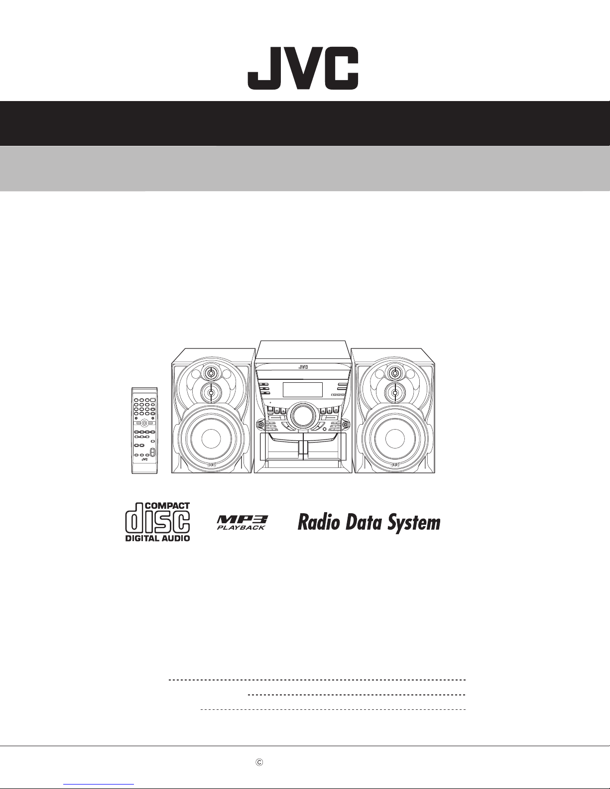
JVC MX-KC45E, MX-KC45EN, MX-KC45A, MX-KC45UW, MX-KC45UY Service Manual
...
SERVICE MANUAL
COMPACT COMPONENT SYSTEM
MB55020067
MX-KC45E,MX-KC45EN,
MX-KC45A,MX-KC45UW,
MX-KC45UY,MX-KC45UJ
Lead free solder used in the board (material : Sn-Ag-Cu, melting point : 219 Centigrade)
1 PRECAUTION. . . . . . . . . . . . . . . . . . . . . . . . . . . . . . . . . . . . . . . . . . . . . . . . . . . . . . . . . . . . . . . . . . . . . . . . . 1-3
2 SPECIFIC SERVICE INSTRUCTIONS . . . . . . . . . . . . . . . . . . . . . . . . . . . . . . . . . . . . . . . . . . . . . . . . . . . . . . 1-5
3 DISASSEMBLY . . . . . . . . . . . . . . . . . . . . . . . . . . . . . . . . . . . . . . . . . . . . . . . . . . . . . . . . . . . . . . . . . . . . . . . 1-6
4 ADJUSTMENT . . . . . . . . . . . . . . . . . . . . . . . . . . . . . . . . . . . . . . . . . . . . . . . . . . . . . . . . . . . . . . . . . . . . . . . 1-12
5 TROUBLESHOOTING . . . . . . . . . . . . . . . . . . . . . . . . . . . . . . . . . . . . . . . . . . . . . . . . . . . . . . . . . . . . . . . . . 1-13
COPYRIGHT © 2006 Victor Company of Japan, Limited
CA-MXKC45 SP-MXKC45SP-MXKC45
TABLE OF CONTENTS
No.MB550
2006/7
SPECIFICATION
Amplifier Output Power (IEC 268-3) 155 W per channel, min. RMS, driven into 6 Ω at 1kHz, with no
more than 10% total harmonic distortion
(DIN-3) 125 W per channel, min. RMS, driven into 6 Ω at 1kHz, with no
more than 0.9% total harmonic distortion
Input Sensitivity/
Impedance (1 kHz)
Cassette Deck Section Frequency Response : Type I (NORMAL) 63 Hz - 12 500 Hz
CD Player CD Capacity 3 CDs
Tuner FM Tuner : Tuning Range 87.50 MHz - 108.00 MHz
Unit Dimensions 270 mm × 307 mm × 492 mm (W/H/D)
Speaker Specifications
(each unit)
Power Specifications Power Requirements AC 240 V , 50 Hz (for Australia)
AUX IN
Speaker terminals
Phones 32 Ω - 1 kΩ
Wow And Flutter 0.15% (WRMS)
Dynamic Range 85 dB
Signal-To-Noise Ratio 85 dB
Wow And Flutter Unmeasurable
AM Tuner : Tuning Range 522 kHz - 1710 kHz
Mass Approx. 9.3 kg
Type 3-way bass-reflex type
Speaker Unit Woofer 16 cm cone × 1
Mid 5cm cone × 1
Tweeter 2cm dome × 1
Power Handling Capacity 160 W
Impedance 6 Ω
Frequency Range 45 Hz - 22 000 Hz
Sound pressure level 87 dB/W·m
Dimensions 220 mm × 324 mm × 238 mm (W/H/D)
Mass Approx. 3.6 kg
Power Consumption 165 W (power on mode)
400 mV/50 kΩ
6 Ω - 16 Ω
17 mW/ch output into 32 Ω
87.50 MHz - 108.00 MHz (at AM9 kHz channel space)
87.5 MHz - 108.0 MHz (at AM10 kHz channel space)
522 kHz - 1 629 kHz (for Europe)
531 kHz - 1710 kHz (at AM9 kHz channel space)
530 kHz - 1710 kHz (at AM10 kHz channel space)
AC 230 V , 50 Hz (for Europe)
AC 110 V-127 V/220 V-240 V , adjustable with voltage selector,
50 Hz/60 Hz (for Asia)
23 W (in Standby mode)
1 W (in ECO mode)
Design and specifications are subject to change without notice.
1-2 (No.MB550)
SECTION 1
PRECAUTION
1.1 Safety Precautions
(1) This design of this product contains special hardware and
many circuits and components specially for safety purposes. For continued protection, no changes should be made
to the original design unless authorized in writing by the
manufacturer. Replacement parts must be identical to
those used in the original circuits. Services should be performed by qualified personnel only.
(2) Alterations of the design or circuitry of the product should
not be made. Any design alterations of the product should
not be made. Any design alterations or additions will void
the manufacturers warranty and will further relieve the
manufacture of responsibility for personal injury or property
damage resulting therefrom.
(3) Many electrical and mechanical parts in the products have
special safety-related characteristics. These characteristics are often not evident from visual inspection nor can the
protection afforded by them necessarily be obtained by using replacement components rated for higher voltage, wattage, etc. Replacement parts which have these special
safety characteristics are identified in the Parts List of Service Manual. Electrical components having such features
are identified by shading on the schematics and by ( ) on
the Parts List in the Service Manual. The use of a substitute
replacement which does not have the same safety characteristics as the recommended replacement parts shown in
the Parts List of Service Manual may create shock, fire, or
other hazards.
(4) The leads in the products are routed and dressed with ties,
clamps, tubings, barriers and the like to be separated from
live parts, high temperature parts, moving parts and/or
sharp edges for the prevention of electric shock and fire
hazard. When service is required, the original lead routing
and dress should be observed, and it should be confirmed
that they have been returned to normal, after reassembling.
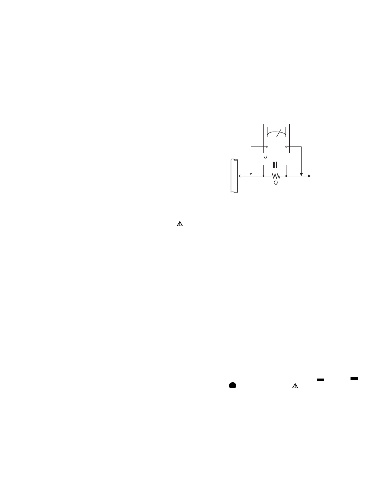
(5) Leakage shock hazard testing
After reassembling the product, always perform an isolation check on the exposed metal parts of the product (antenna terminals, knobs, metal cabinet, screw heads,
headphone jack, control shafts, etc.) to be sure the product
is safe to operate without danger of electrical shock.Do not
use a line isolation transformer during this check.
• Plug the AC line cord directly into the AC outlet. Using a
"Leakage Current Tester", measure the leakage current
from each exposed metal parts of the cabinet, particularly any exposed metal part having a return path to the
chassis, to a known good earth ground. Any leakage current must not exceed 0.5mA AC (r.m.s.).
• Alternate check method
Plug the AC line cord directly into the AC outlet. Use an
AC voltmeter having, 1,000Ω per volt or more sensitivity
in the following manner. Connect a 1,500Ω 10W resistor
paralleled by a 0.15µF AC-type capacitor between an ex-
posed metal part and a known good earth ground.
Measure the AC voltage across the resistor with the AC
voltmeter.
Move the resistor connection to each exposed metal
part, particularly any exposed metal part having a return
path to the chassis, and measure the AC voltage across
the resistor. Now, reverse the plug in the AC outlet and
repeat each measurement. Voltage measured any must
not exceed 0.75 V AC (r.m.s.). This corresponds to 0.5
mA AC (r.m.s.).
AC VOLTMETER
(Having 1000
ohms/volts,
or more sensitivity)
0.15 F AC TYPE
Place this
probe on
1500 10W
Good earth ground
1.2 Warning
(1) This equipment has been designed and manufactured to
meet international safety standards.
(2) It is the legal responsibility of the repairer to ensure that
these safety standards are maintained.
(3) Repairs must be made in accordance with the relevant
safety standards.
(4) It is essential that safety critical components are replaced
by approved parts.
(5) If mains voltage selector is provided, check setting for local
voltage.
1.3 Caution
Burrs formed during molding may be left over on some parts
of the chassis.
Therefore, pay attention to such burrs in the case of preforming repair of this system.
1.4 Critical parts for safety
In regard with component parts appearing on the silk-screen
printed side (parts side) of the PWB diagrams, the parts that are
printed over with black such as the resistor ( ), diode ( )
and ICP ( ) or identified by the " " mark nearby are critical
for safety. When replacing them, be sure to use the parts of the
same type and rating as specified by the manufacturer.
(This regulation dose not Except the J and C version)
each exposed
metal part.
(No.MB550)1-3
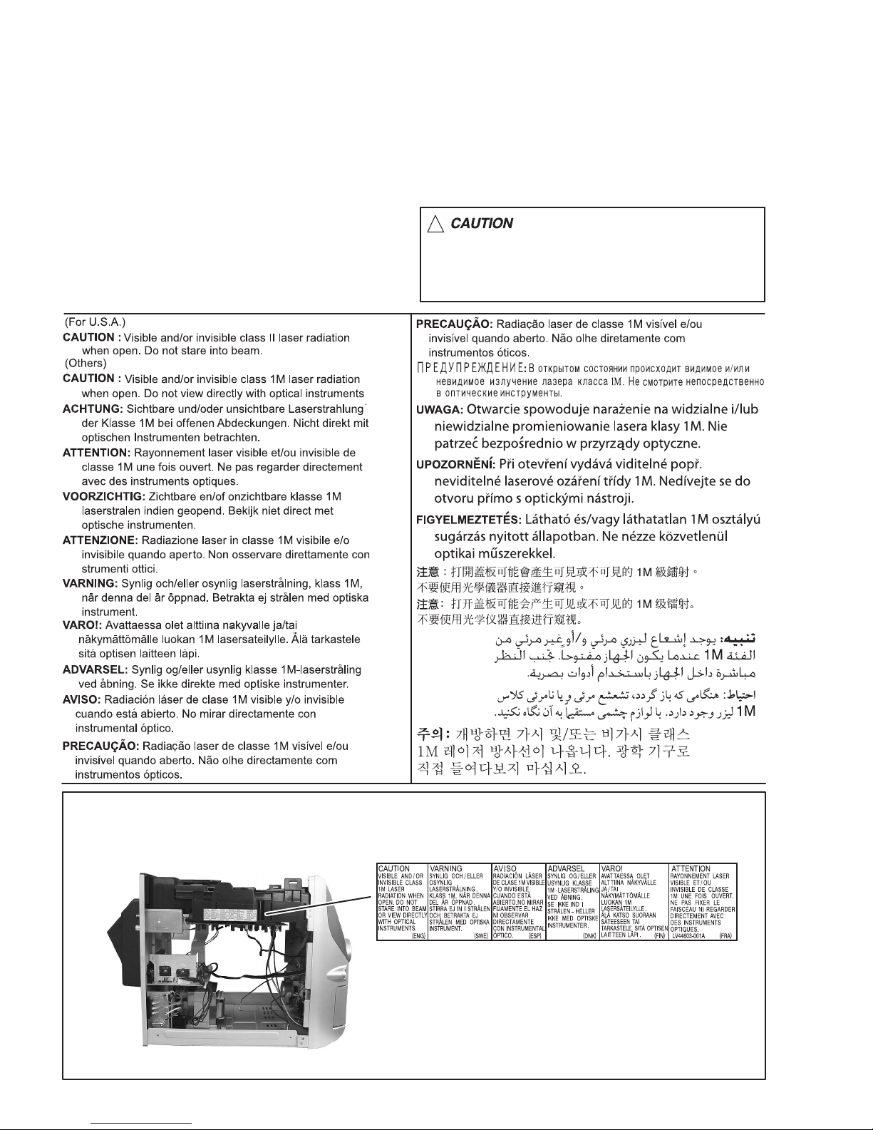
1.5 Important for laser products
1.CLASS 1 LASER PRODUCT
2.CAUTION :
(For U.S.A.) Visible and/or invisible class II laser radiation
when open. Do not stare into beam.
(Others) Visible and/or invisible class 1M laser radiation
when open. Do not view directly with optical instruments.
3.CAUTION : Visible and/or invisible laser radiation when
open and inter lock failed or defeated. Avoid direct
exposure to beam.
4.CAUTION : This laser product uses visible and/or invisible
laser radiation and is equipped with safety switches which
prevent emission of radiation when the drawer is open and
the safety interlocks have failed or are defeated. It is
dangerous to defeat the safety switches.
5.CAUTION : If safety switches malfunction, the laser is able
to function.
6.CAUTION : Use of controls, adjustments or performance of
procedures other than those specified here in may result in
hazardous radiation exposure.
!
Please use enough caution not to
see the beam directly or touch it
in case of an adjustment or operation
check.
REPRODUCTION AND POSITION OF LABELS and PRINT
WARNING LABEL and PRINT
1-4 (No.MB550)

SECTION 2
SPECIFIC SERVICE INSTRUCTIONS
This service manual does not describe SPECIFIC SERVICE INSTRUCTIONS.
(No.MB550)1-5
SECTION 3
DISASSEMBLY
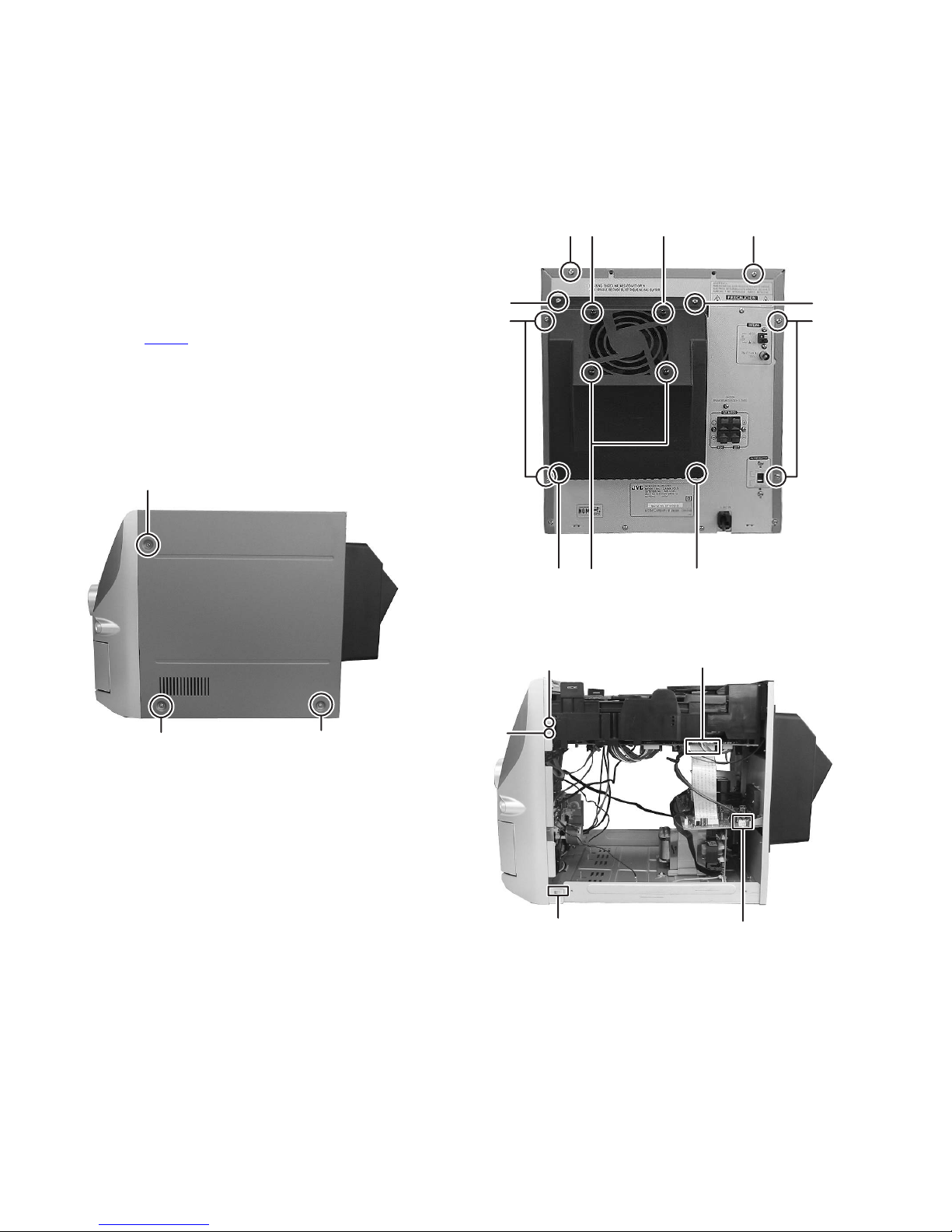
3.1 Main Body
3.1.1 Removing the metal cover
(See Fig.1, 2)
(1) Remove the two screws A and four screws B attaching the
metal cover from both side of the main body. (See Fig.1)
(2) Remove the six screws C attaching the metal cover from
back side of main body. (See Fig.2)
3.1.2 Removing the heat sink cover
(See Fig.2, 3)
(1) Disconnect the connector wire from the fan connected to
connector CN603
(2) Remove the four screws D attaching the heat sink cover.
(See Fig.2)
3.1.3 Removing the fan
(See Fig.2)
(1) Remove the four screws E attaching the fan.
of the amp board. (See Fig.3)
A
CE E C
DD
CC
BB
(both side)
Fig.1
G
DDE
G
a
Fig.2
CN601
CN603
Fig.3
1-6 (No.MB550)
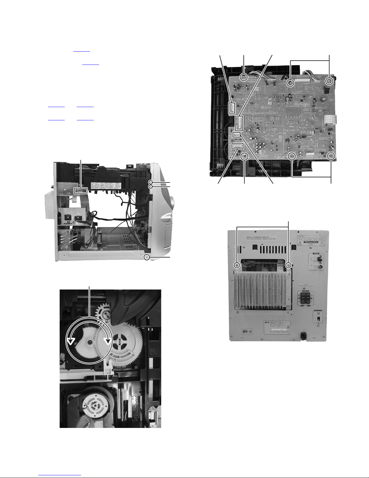
3.1.4 Removing the 3CD changer mechanism
(See Fig.3 to 7)
(1) Disconnect the card wire from amp board connected to the
connector CN601
(2) Disconnect the card wire from the tuner pack connected to
the connector CN306
(3) Open the CD tray and remove the CD door.
Caution:
If the CD tray can not open at power to ON condition, rotate the gear and open the CD tray. (See Fig.5)
(4) Disconnect the card wire connected to the connector
and CN303 of the main board. (See Fig.6)
CN201
(5) Disconnect the connector wire connected to the connector
and CN302 of the main board. (See Fig.6)
CN301
(6) Remove the two screws F attaching the 3CD changer
mechanism of back side of the main body. (See Fig.7)
(7) Remove the four screws G attaching the 3CD changer
mechanism from both side of the main body. (See Fig.3, 4)
of the main board. (See Fig.3)
of the main board. (See Fig.4)
CN306
CN303
HH
CN201
Fig.4
GEAR (top view)
G
Q
CN302 CN301
HH
Fig.6
Fig.7
F
Fig.5
(No.MB550)1-7
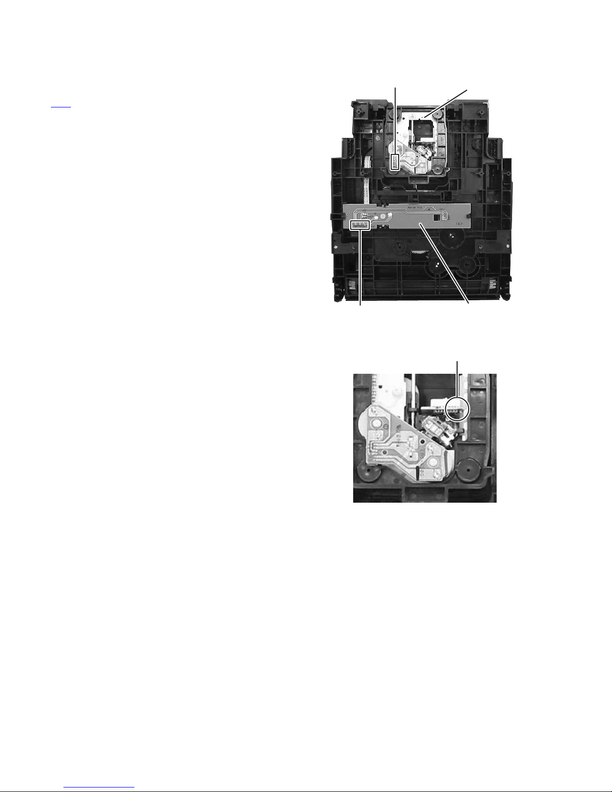
3.1.5 Removing the main board
(See Fig.6, 8, 9)
(1) Remove the six screws H attaching the main board. (See
Fig.6)
(2) Disconnect the connector wire connected to the connector
of the motor board. (See Fig.8)
CW3
(3) Disconnect the connector wire connected to the connector
of the traverse mechanism. (See Fig.8)
(4) Solder the short land section of the CD pickup and then dis-
connected the card wire from the main board connected to
the CD pickup. (See Fig.9)
Caution:
• Solder the short land section of the CD pickup before disconnecting the card wire from the connector on the CD pickup.
If the card wire is disconnected without attaching the solders, the pickup may be destroyed by static electricity.
• When attaching the CD pickup, be sure to remove solders
from the short land section after connecting the card wire to
the connector on the CD pickup.
connector wire
traverse mechanism
CW3
motor board
Fig.8
short land section
Fig.9
1-8 (No.MB550)

3.1.6 Removing the tuner pack
(See Fig.11)
(1) Remove the two screws J attaching the tuner pack.
3.1.7 Removing the amp board
(See Fig.10, 11)
(1) Disconnect the connector wire from the front board con-
nected to the connector CN202
Fig.10)
(2) Disconnect the connector wires from the power transform-
er connected to the connector CN902
amp board. (See Fig.10)
(3) Remove the four screws K attaching the amp board. (See
Fig.11)
(4) Remove the three screws L attaching the amp board. (See
Fig.11)
3.1.8 Removing the voltage selector board
(See Fig.11)
(1) Remove the two screws M attaching the voltage selector
board.
3.1.9 Removing the rear panel
(See Fig.11)
(1) Remove the four screws N attaching the rear panel.
of the amp board. (See
and CN903 of the
CN202 CN903CN902
Fig.10
K
K
K
J
L
L
L
M
N
Fig.11
(No.MB550)1-9

3.1.10 Removing the front panel assembly
(See Fig.3, 4, 12, 13)
(1) Disconnect the two earth wires from the bottom plate. (See
Fig.12)
(2) Remove the one screw P attaching the front panel assem-
bly from bottom side. (See Fig.13)
(3) Remove the two screws Q attaching the front panel assem-
bly from both side of the main body. (See Fig.4)
(4) Disengage the hook a on the both side of the front panel
assembly. (See Fig.3)
earth wire
Fig.12
P
Fig.13
1-10 (No.MB550)
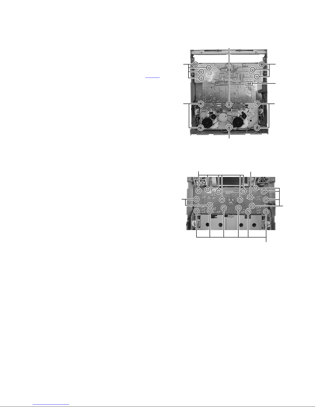
3.1.11 Removing the cassette mechanism assembly
(See Fig.14)
(1) Remove the six screws R attaching the cassette mecha-
nism assembly.
3.1.12 Removing the front board
(See Fig.14, 15)
(1) Remove the seven screws S attaching the front board.
(See Fig.14)
(2) Disconnect the connector wire from the connector CN201
of the front board. (See Fig.14)
(3) Remove the main volume knob.
(4) Remove the eighteen screws T attaching the front board.
(See Fig.15)
(5) Remove the one screws U attaching the front board. (See
Fig.15)
R
SS
CN201
RR
R
Fig.14
T
T
U
T
T
Fig.15
(No.MB550)1-11

SECTION 4
ADJUSTMENT
This service manual does not describe ADJUSTMENT.
1-12 (No.MB550)

SECTION 5
TROUBLESHOOTING
This service manual does not describe TROUBLESHOOTING.
(No.MB550)1-13

Victor Company of Japan, Limited
Audio/Video Systems Category 10-1,1chome,Ohwatari-machi,Maebashi-city,371-8543,Japan
(No.MB550)
Printed in Japan
VPT
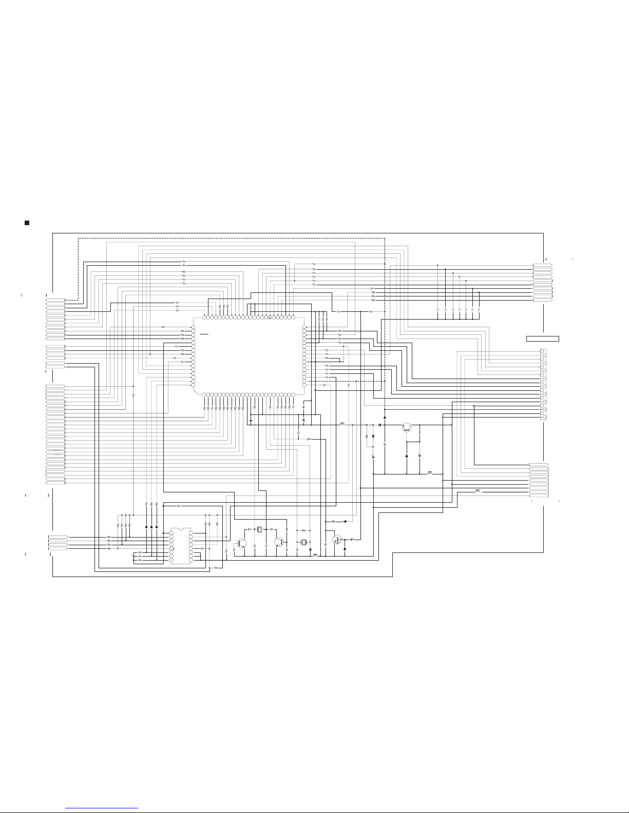
SCHEMATIC DIAGRAMS
COMPACT COMPONENT SYSTEM
MX-KC45E,MX-KC45EN,MX-KC45A
MX-KC45UW,MX-KC45UY,MX-KC45UJ
CD-ROM No.SML200607
Lead free solder used in the board (material : Sn-Ag-Cu, melting point : 219 Centigrade)
Contents
Block diagrams
Standard schematic diagrams
Printed circuit boards
CA-MXKC45 SP-MXKC45SP-MXKC45
COPYRIGHT 2006 Victor Company of Japan, Limited.
2-1
2-2
2-17 to 21
No.MB550SCH
2006/7

In regard with component parts appearing on the silk-screen printed side (parts side) of the PWB diagrams, the
parts that are printed over with black such as the resistor ( ), diode ( ) and ICP ( ) or identified by the " "
mark nearby are critical for safety.
2-1
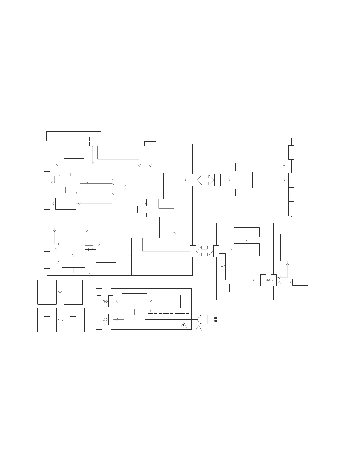
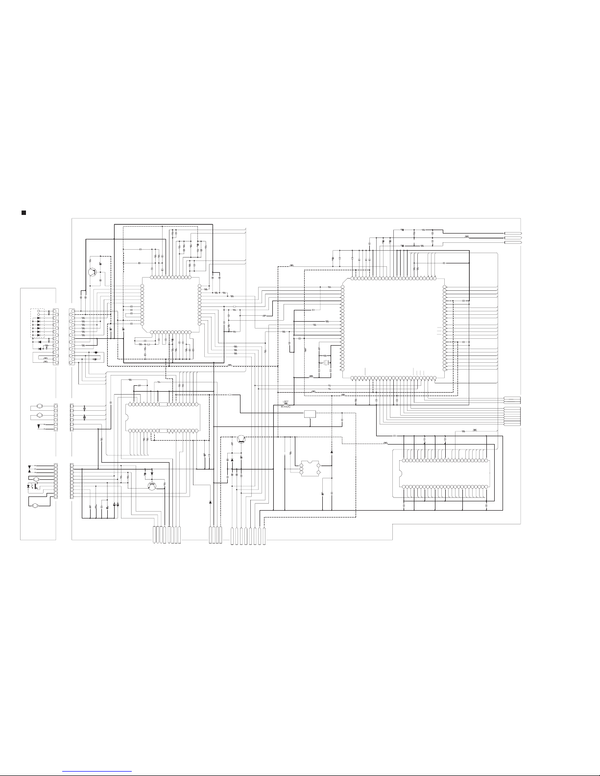
Block diagram
Q414 to Q419
MECHA
CONTROL
JOG KEY'S
CON1
CN205
ANT IN
DECK-A
PB-HEAD
TO
DECK-B
R/P-HEAD
TO
CASSETTE
MECHANISM
TO
CD PICKUP
TO
SPINDLE
SLEED
TO
CD MECHA
TRANSFORMER PWB
TO AMP
AC IN
TO
HEADPHONE
CW202
SPEAKER
OUT
TO
PT PWB
CW903
TO
PT PWB
CW902
AUX IN
AUX JACK
TUNER L
TUNER R
CLK,CE
DAT IN/OUT
A/B SEL
BIAS-ON
SOL-A
SOL-B
MOTOR-ON
TAPE L
TAPE R
SENCE
MLT
MRD/MDATA
MWR/MCK
CD ON
MOTOR-MUTE
IN-SW
CAM+
LD M+
LD M-
XRST
DSP-SENSE
DECINT
MDO
MADDR
MD0 to MD7
SDIN,SCLK,SENB
REMOTE,P-CNT
ENCONDER1
ENCONDER2
KEY1,KEY2,KEY3
PRE-AMP L
PRE-AMP R
L OUT
R OUT
AUX L
AUX R
CD L
CD R
VOLUME
PT901
TRANSFORMER
IC702
IC701
CD RF AMP
CN301CN302CN303CN701CN702CN703
Q434,Q435
BIAS OSC
IC601
2CH
POWER AMP.
Q611
MUTE
Q612
MUTE
CN202JK601CN903CN902
IC803
16M
SDRAM
IC804
DIGITAL
SERVO
IC301
MCU
IC202
VFD DRIVER
VFD
IC201
IR SENSOR
PT902
BACKUP PT
S901
VOLTAGE
SELECTOR
CN902 CN903
CW903CW902
MAIN
CN205
AUX
CW205
AMP
CN202
HEAD PHONE
CW202
IC401
VOLUME
Q401 to Q410
Q438
A/B DECK
EXCHANGE
Q420,Q421
VOL DATA
CN306
TUNER PARK
CN201 CN601
CW601
CW201
CW215
CW203
PHONE JACK
Used for Area suffix UW/UY/UJ
2-2
Parts are safety assurance parts.
When replacing those parts make
sure to use the specified one.
Standard schematic diagrams
S3
GND
S3
S1
S2
GND
S2
S1
8
7
6
5
4
3
2
1
CON - 2.5 - 8P
CN2
C601
C602
0.1U
0.1U
1N4003
D605
1N4003
D603
1N4003
D606
33(1 / 2W)-FR
D602
1N4003
RF601
R672
33(1 / 4W)
D601
1N4003
Q604
KTB1366Y
Q605
2SC3052
C604
0.1U
R601
4.7K
C605
C607
4700 / 25
R605
1K
100 / 25
D607
UZ12BSC
C608
0.1U
C609
100 / 16
D608
NM
0.1U
C603
4.7K
R101
C101
1000 / 25
R103
22K
R104
22K
Q101
2SC3052
C102
100 / 10
R102
2.2K
Q102
2SC3052
C610
47 / 63
R606
3.3K
D631
1SS133
Q607
KTA1273Y
R607
2.2K
C611
22 / 50
C612
0.01U
D609
UZ30BSD
D610
UZ6.2BSB
C614
10 / 25
C613
22 / 50
R671
5.6K(A)
R608
100(A)
R609
100(A)
F2
F1
[1]
47K(A)
R683
C617
682(M)
C618
682(M)
R682
33K(A)
C619
682(M)
C620
682(M)
TO POWER PCB
RF602
JW
Q608
KTB1366Y
Q609
2SC3052
R610
150K
R669
1.2K
Q610
2SC3052
R611
56K
C615
0.01U
R612
D611
4.7K
UZ5.6BSB
R600
820
C616
470 / 10
D612
NM
D613
1N4003
D614
AC
AC
AC
AC
D615
RS402
R681
33K(A)
R684
47K
GBU6J
[ AMP PCB ]
C622
C621
682(M)
682(M)
C624
4700 / 50
C623
4700 / 50
C626
3300 / 71
C628
682(M)
C625
3300 / 71
C627
682(M)
R614
100(1 / 2W)
C630
562(M)
C632
100 / 100
R613
100(1 / 2W)
C629
562(M)
D616
UZ12BSC
C631
100 / 100
1.5K(1 / 2W)
R615
R616
1.5K(1 / 2W)
D617
UZ12BSC
VH+
VL+
P+VL
P-VL
VL-
VH-
1
23
4
5
6789
SUB
OUT1+
OUT1-
10
11
12
13
14
15
16
17
18
IN2
NF2
BIAS
NF1
IN1
PRE+VCC
PRE-VCC
OUT2+
OUT2-
C635
100 / 10
C637
R617
560
3P
R618
JW
R619
33K
C633
100P
R620
33K
C636
100 / 10
R621
560
C634
100P
C638
R622
JW
3P
R623
33K
R625
56K
R624
56K
C639
1000P
C640
1000P
R627
4.7K
R626
4.7K
R630
R631
3.9K
C641
4.7 / 50
Q611
DTC323TK
R628
2.2K
C642
4.7 / 50
3.9K
Q612
DTC323TK
R629
2.2K
A05
D109
MC2838
33K
R120
R121
33K
C117
R123
1K 100 / 16
R124
C118
1K
100 / 16
D101
1N4003 D102
1N4003 D103 1N4003
R110
2.2
IC601
STK412 - 040
FAN DRIVE
KTA1273Y
Q111
R112
470
Q112
2SC3052
C114
R116
1 / 50
R115
220K
47K
C113
100 / 10
R113
1SS133
1K
47 / 16
R114
56
D105
C115
Q114
KTA1273Y
D106
R117
470
1SS133
R118 1K
Q113
2SC3052
D107
1SS133
R119
1K
D108
1SS133
C116
100 / 16
CN603
CON - 2.5 - 3P
1
2
3
FAN+
FAN-
FAN+
FPC-1.25-24P
A06
A01
A03
A04
A02
C655
0.015U
C656
0.015U
NM
NMNMNM
C661
C660
C659
C658
CN202
TO FRONT PCB
Q623
DTC323TK
R664
1K
R663
10K
R662
1K
Q622
DTC323TK
R661
10K
Q619
DTC114YK
R655
10K
R654
1K
1SS133
1SS133
D625 D624
R656
15(A)
Q618
2SC3052
R665
1K(2W)
R653
0
D626
1SS133
R666
1K(2W)
RY601
ME - 7C - 012 - 2H
NM
R647
470K
1 / 50
C644
D620
1SS133
470
R646
4.7 / 50
C643
10K
R645
10K
R644
L601
3UH(R)
R640
4.7(1/4W)
R641
4.7(1/4W)
L602
3UH(R)
Q613
KTA1267G
R642
1K
C645
0.1U(M)
C646
0.1U(M)
R648
4.7(1/4W)
C647
0.1U(M)
C648
0.1U(M)
R649
4.7(1/4W)
C650
47 / 16
R650
100K
R651
100K
R652
100K
R643
1K
C649
120P
Q614
KTA1267G
Q615
2SD3052
Q616
2SC3052
D623 1SS133
C652
22 / 50
Q617
2SC3052
C651
0.022U
R658
47K
D621
1SS133
R657
680K
C653
220 / 10
R659
2.2K
A05
DTA114YK
Q621
DTA114YK
Q620
C654
10 / 25
R660
3.9K
D622
1SS133
A[01:10]
A06
A04
Q624
DTC114YK
Q601
2SC3052
CN602
1
2
TH601
10K
C606
1 / 50
R602
75
ATTACH TO HEATSINK
R632
R633
R634
R635
0.15(3W)
0.15(3W)
0.15(3W)
0.15(3W)
R636
R637
1K
1K
D618
1SS133
D619
1SS133
R638
15K
15K
R639
CW902
CON - ASSY2.0 - 6P
1
2
3
4
5
6
1
2
3
4
5
6
V-ECO
INH
GND
RELAY ON
AC3.3V
AC3.3V
A03
A02
A01
CN902
CON - 2.0 - 6P
[1]
[1]
F2
F1
Q901
DTC114YS
C907
3.3 / 50
R902
D906
4.7K(A)
1SS133
C905
470 / 25
D905
C904
D904
C903
D903
C902
D902
C901
1SS133
223
1SS133
223
1SS133
223
1SS133
223
R901
10(A)
D901
1SS133
[ P / T PCB ]
PT-SUB
PT902
1
2
3
PRIMARY
RY901
PT-MAIN
8
3
2
4
9
10
11
12
13
6
14
15
16
17
FC901
PT901
NATURAL
LIVE
T2AL
250V
C951
0.22 / 275V
TB901
TB902
F901
AC - CORD
1
2
3
4
5
6
7
8
CW903
CON - ASSY2.5 - 8P
S1
S2
GND
S2
S1
S3
GND
S3
FC902
C908
NM
RELAY(ME-7)
FILTER-AC
L901
1
2
3
4
HP-L
GND
HP-R
HP-SW
JK601
SP-4P(PST-404)
SP-L
GND
SP-R
GND
1
2
3
4
[1]
1
2
3
FAN1
FAN DC12V
CW601
M
1
2
3
4
5
6
7
8
9
10
11
12
F1
VFP
F2
SAFTY
RELAY ON
V-ECO
S-MUTE
INH
SPK-RLY
PROTECTE
5V
5V
DGND
DGND
+12V
+12V
M-GND
M-GND
AGND
AGND
- VEE
L-IN
AGND
R-IN
13
14
15
16
17
18
19
20
21
22
23
24
TO MAIN PCB
C699
0.1U
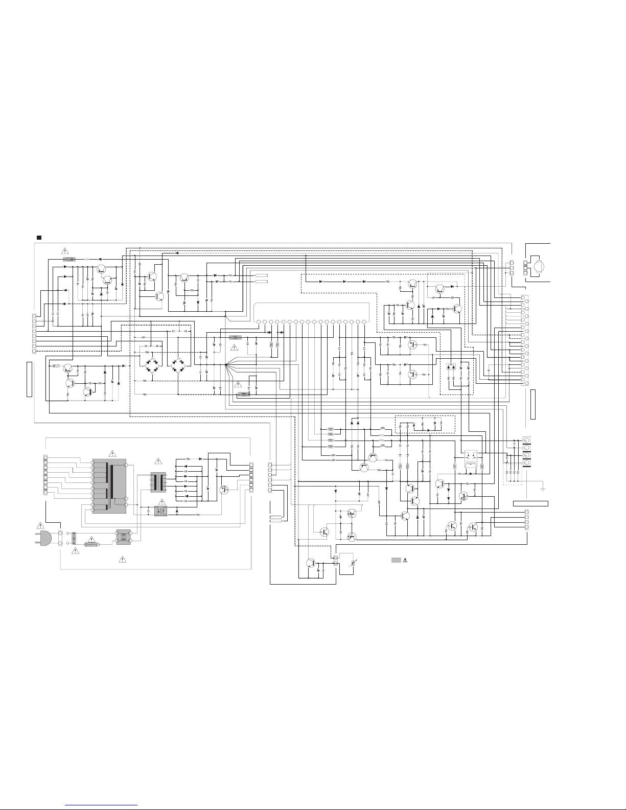
Amplifier section
For E,EN version
2-3
Main section
HEAD-PLAY
L.CH
R.CH
HEAD-PLAY
CN301
CON - 2.0 - 3P
1
2
3
1
2
3
C401
1200P
R401
39K
C402
1200P
R402
39K
Q401
2SJ460
D
S
G
D
S
G
100(A)
R403
R404
100
2SJ460
Q402
Q403
2SK2541
D
S
G
DS
G
2SK2541
Q404
C429
C426
1200P
1200P
R421
82K
R422
82K
C463
0.1U
Q405
2SJ460
D
S
G
D
S
G
A406
2SJ460
C430
1000P
D
S
G
D
S
G
D
S
G
Q407
2SK2541
C408
470P
D401
MC2836
Q409
2SK2541
R423
220K
R425
2.2K
Q410
SPA2202S
2R
R424
22K
Q408
2SK2541
R575
100(A)
R515
R514
39K
39K
R407
NM
C405
R405
100 / 10V
150
R409
390K(A)
C411
470P
R413
18K
R414
18K
C412
470P
R416
47K
R415
47K
R418
1K
R420 1K
C418
2.2 / 50V
C407
2.2 / 50V
D405
UZ4.7BSA
C417
220 / 10V
R411
C409
6800P
1.2K
R412
C410
6800P
1.2K
R410
390K
C406R406
150
100 / 10V
R408
NM
C414
560P
C415
560P
C404
CH
47P
C403
47P
CH
C413
100 / 10V
D402
UZ4.7BSA
C419
C416
3300P
3300P
R574
10K
C424
C423
0.1U
0.1U
R.CH
L.CH
HEAD-R/P
HEAD-R/P
HEAD-ERASE
CN302
8
7
6
5
4
3
2
1
8
7
6
5
4
3
2
1
CON - 2.0 - 8P
C453
R463
CH
1000P
1K
C454
1000P
CH
R464
1K
R429
12K(A)
R428
12K(A)
Q438
DTC114TK
R427
2.2K
C427
180P
R431
2.2K
R433
10K
C434
180P
R557
10K
R426
2.2K
R438
2.2K
C433
2200P
R435
C435
1K
0.01U
R437
1K
C437
6800P
R439
1.8K
R430
1.8K
R436
1K
C448
6800P
C436
R434
1K
0.01U
C444
2200P
T401
COIL - REC - OSC - 6P(85KHZ)
R417
47(1/4W)
6
5
4
1
2
3
S
S
R512
2.2K(A)
R528
10K
Q433
2SC3052
C521
560P(A)
C503
6800P(M)
C440
200 / 16V
C432
0.01U
R419
8.2(1/4W)
Q434
2SC5343
R461
18K
C520
2700P
C518
2700P
Q435
2SC5343
R460
18K
C441
2700P
2
1
3
5
4
678
9
101112
13
14
28
27
26252423222120
19
18
171615
IC401
BD3881FV
PBIN-L
PBIP-L
PB2P-R
PB2N-R
PB2O-R
PB1O-L
VOL-IN-L
VOL-IN-R
GND
TRE1-L
TRE2-R
VDD
CONT
VEE
REC1O-L
REC1N-L
REC2N-R
REC2O-R
TU-IN-R
TU-IN-L
CD-IN-R
CD-IN-L
AUX-IN-R
AUX-IN-L
OUT-L
BASS1-L
OUT-R
BASS2-R
R598
220(A)
R573
220(A)
R597
R572
470(1/4W)
4.7K(A)
R571
470(1/4W)
C421
100P
Q420
2SC3052
R570
4.7K
Q421
2SC3052
R442
3.3K
R443
3.3K
[3]
[3]
[3]
CD-AGND
CD-LCH
CD-RCH
C510
1 / 50V
C506
1 / 50V
R503
R504
22K(A)
22K(A)
[1]
[1]
[1]
[1]
[1]
[1]
[1]
TU-ON
TU-CE
TU-DATA
TU-CLK
TU-DIN
RDS-DA
RDS-CK
R539
2.2K
R538
2.2K
R541
4.7K
R540
4.7K
C539
1000P
R441
15K
C536
1000P
R440
15K
C547
0.1/50V
R501
15K(A)
C546
0.1/50V
R502
15K(A)
12
11
10
9
8
7
6
5
4
3
2
1
RDS 3.3V
RDS CLK
RDS DATA
TUNED
TU-D-OUT
TU CLK
TU-D-IN
TU CE
+9V
R-ch OUT
A GND
L-ch OUT
CN306
FPC-1.25-12P
TO TUNER UNIT
E VERSION: CN306 12P
OTHER VERSION: CN306 10P
L505
BEAD(A)
R581
3.3K
R580
100K
C535
47/16V
2SC3052
Q422
D509
1SS133
R578
Q423
KTA1267G
470(A)
L511
BEAD(A)
R579
47(A)
D517
C458
47U/16
R479
12(1/4W)
1
RDS-ON
560(A)
R582
Q521
DTA114TK
D521
UZ3.3B
C551 47/16V
DTC114TK
Q522
R505
39K
C541
100P
R457
4.7K(A)
C545
4.7 / 50
R508
4.7K(A)
R506
39K
C540
100P
C544
4.7 / 50
CN205
1
2
3
AUX-L
A-GND
AUX-R
TO AMP PCB
GAIN-CTRL
[1]
[1]
S-BOOST
U - VERSION ONLY
R546
5.6K
470
R548
[1]
[1]
[1]
[1]
[1]
[1]
[1]
[1]
[1]
[1]
[1]
5V
P-CNT
AC-IN
PRT
SPK
INH
S-MUTE
AC-SW
F2
VFP
F1
R368
150K(A)
[ TO MICOM PART ]
R325
120K(A)
D506
D507
R478
2.2K(A)
Q411
KTA1267G
R432
1.5K(A)
C519
R534
10K
JW
Q424
KTC3199
C502
100 / 16
R452
4.7K(A)
R454
100(A)
R453
1.2K(A)
CN601
FPC - 1.25 - 24P
F1
VFP
F2
SAFTY
AC-SW
V-ECO
S-MUTE
INH
SPK-RLY
PROTECTE
5V
5V
DGND
DGND
+12V
+12V
M-GND
1
2
3
4
5
6
7
8
9
10
11
12
13
14
15
16
17
18
M-GND
AGND
19
20
21
22
23
24
AGND
- VEE
L-IN
AGND
R-IN
TO AMP PCB
DGND
0.1U
C561
R566
6.8K
D508
1SS133
R567
3.3K
Q508
2SC1815GR
R484
470
C528
47U / 16
D516
UZ11BSB
D511
1SS133
1SS133
D502
[3]
[3]
[1,3]
[3]
[3]
SW+5V
CD+5V
CD-DGND
CD-MGND
CD-12V
L503
BEAD(A)
TO CDP PART
[ MAIN PCB - 2 / 3 ]
R547
5.6K
470
R549
Q425
KTC3199
R533
10K(A)
Q413
DTC114TK
R469
10K
Q412
DTC114TK
IC403
KIA78L05BP
31
2
D406
1SS133
Out
In
Gnd
1SS133
D407
C431
100 / 10V
3.9K
R550
R542
10K
C460
0.22 / 50V
R480
1K
R482
47K
C462
1000P
3.9K
R537
R543
10K
R481
1K
C459
0.22 / 50V
R483
47K
C461
1000P
R586 0
R585 0
C527
22 / 25V
C501
22 / 25V
R525
100K
100K
R526
68K
R465
R509
68K
C425
0.1 / 50V
C497
0.068U
R523
2.2K
C445
0.47 / 50V
C420
0.1 / 50V
C496
0.068U
C422
0.47 / 50V
R507
2.2K
R459
2.2K
R462
47K
Q436
2SC5343
Q437
2SC3052
R511
4.7K(A)
R458
4.7K
R510
5.6K
C438
0.1U
5.6K
R513
56K
C428
220 / 16V
R577
2.2K
R576
2.2K
R521
0
R522
NM
C524
1 / 50
R519
100K
R518
100K
R520
10K
R517
1.2K
D501
1SS133
C525
4.7 / 50
1 / 50
C526
R516
330K
Q501
2SC3052
D510
1N4001
D503
1SS133
R564
JW
Q506
KTA1267G
R562
22K
Q505
DTC114TK
R560
22K
Q507
DTC114TK
R563
470
D504
1SS133
100 / 10
C557
0.01U
C558
1SS133
D505
R561
22K
Q504
KTA1267G
Q509
DTC114TK
R559
47K
C560
NM
4.7K
R558
[1]
[1]
[1]
[1]
[1]
[1]
[1]
[1]
[1]
[1]
[1]
[1]
[1]
[1]
[1]
[1,3]
CD-ON
SAFETY
L-METER
SCL-CTL1
SDA-CTL2
A / B-SEL
BIAS-ON
BEAT-CUT
TO MICOM
SOL-A
SOL-B
MOTOR-ON
DET-B
DET-A
REC-B
HALF-A / B
AVREF(3.3V)
L509
BEAD(A)
C446
0.01U
100 / 16
C447
Q415
KTA1273
C439
0.01U
Q414
2SC3052
D404
1SS133
3.3K(A)
R444
4.7K
R445
150
R446
Q417
KTA1273
C449
0.01U
Q416
2SC3052
Q419
KTA1273
Q418
DTC114K
D403
1SS133
4.7K
R448
R447
3.3K(A)
R449
150
3.3K
R450
4.7 / 50
C450
R451
1K
C451
100 / 16
R472
56K
R468
2.2K
R467
2.2K
R471
12K
R455 47K
R456 22K
CN303
FPC - 1.25 - 9P
A-SOL
A-REEL
A-HALF
+12V
REC-SW
GND
B-HALF
B-REEL
B-SOL
1
2
3
4
5
6
7
8
9
1
2
3
4
5
6
7
8
9
M
2-4
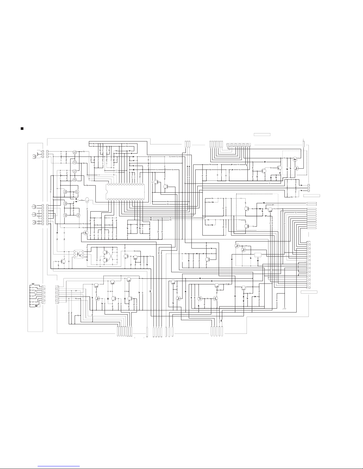
Micon section
TO DECK PART
[2]
AVREF(3.3V)
[2]
SCL-CTL1
SDA-CTL2[2]
REC-MUTE
PB-MUTE
[2]
SOL-A
[2] SOL-B
[2]
[2]
[2]
[2]
MOTOR-ON
BIAS-ON
A / B-SEL
BEAT-CUT
[2]
[2]
[2]
[2]
[2]
[2]
SPK
S-BOOST
P-CNT
S-MUTE
L-METER
SAFETY
TO AMP PART
[3]
[3]
[3]
[3]
[3]
[3]
IN-SW
EMITTER
SW2
SW1
CAM+
LD_M+
LD_M-
[3]
[3]
[2,3]
[3]
[3]
MOTOR-MUTE
CD-ON
MD0
MD1
MD2
MD3
MD4
MD5
MD6
MD7
[3]
[3]
[3]
[3]
[3]
[3]
[3]
[3]
[3]
[3]
[3]
[3]
[3]
[3]
[3]
MADDR
MCS
MWR / MCK
MRD / MDATA
DECINT
DSP-SENSE
SENSE
MLT
XRST
TO CDP PART
TO DECK PART
[2]
[2]
[2]
[2]
DET-A
HALF-A/B
REC-B
DET-B
R373
R374
R375
R376
0
0
0
0
R393
R394
R395
10K
10K
10K
R377
R378
R379
R380
2.2K
2.2KNM2.2K
D309
D308
D307
1SS133
1SS133
1SS133
R396
R397
R398
1K
1K
1K
C308
0.1U
IC302
BU4051
16
15
14
13
12
11
10
9
1
2
3
4
5
6
7
8
VDD
DET-A
HARF-A/B
REC-B
DET-B
A
B
C
SFT
INH
VEE
VSS
G-EQ
ACIN
COM
OPTION
R385
1K
R399
22K
R381
NM
R382
10K
R384
3.3K
R371
47K
C310
NM
Q301
NM
C309
NM
XT302
8MHz
C311
27P
C312
24P
C313
33P
Q302
2SC3052
R388
2.2K
C314
1000P
R389
C315
22P
C316
22P
XT301
32.768KHZ
L304
BEAD
C320
NM
R390
47K
D301
1SS133
Q303
DTC114YK
C318
1/50
D302
1SS133
R346
R347
100(A)
100(A)
R356
R357
R358
R359
100(A)
100(A)
100(A)
R355
R348
R351
1K(A)
1K(A)
R392
10K(A)
R350 1K
R360
220
R361
470
R362
470
R363
470(A)
R364
R365
100
100(A)
1K(A)
R366
R367
1K
1K
0
R354
R353
R352
0.1U
C301
64
63
62
61
60
59
58
57
56
55
54
535251
504948
474645
444342
41
40
39
38
37
36
35
34
33
32
31
30
29
28
27
24
26
25
23
22
21
20
19
18
17
16151413121110
1
2
3
456
7
8
9
65
66
67
68
69
70
71
72
73
74
75
76
77
78
79
80
IC301
S3C825A
SW2
BIAS-ON
A/B-SEL
BEATCUT
CLOCK-SFT
SPK
NC(B-BOOST)
P-CNT
S-MUTE
MOTOR-MUTE
CSB
CLKB
DIN
A
B
C
SW1
INH
IN-SW
REC-MUTE
LD_M-
LD_M+
CAM+
MOTOR-ON
SOL-B
SOL-A
PB-MUTE
VDD2
VSS2
VCL1
TU-CE
TU-DATAOUT
TU-CLK
CD-ON
MD0
MD1
MD2
MD3
MD4
MD5
MD6
MD7
MADDR
MCS
VDD
VSS1
XOUT
XIN
TEST
XTIN
TU-DATA IN
TUNER-ON
PRT(SP)
AC-SW
SDA(VOL)
SCL(VOL)
RDS
DATA
XTOUT
RESET
MWR/MCK
MRD/MDATA
DECINT
SCOR
SENSE
RDS-CLK
REMOCON
EMITTER
ENCODER
ENCODER
XRST
GAIN CONTROL
RDS ON
SUBQ
AVSS
KEY3
KEY2
KEY1
AD-IN
AVREF
MLT
R387
R345
R344
R343
R342
R341
10K(A)
1K(A)
220(A)
220(A)
220(A)
1K(A)
R336
R335
R334
22K
22K
22K
R331
2.2K(A)
R340
R339
470(A)
330
R338
100
R337
100
R333 1.8K(A)
R332
R349
R330
R329
2.2K
1K(A)
2.2K
2.2K(A)
R327
100(A)
R370 100(A)
0R326
(OPTION:RM)
C319
0.1U(A)
R324
R323
R322
R321
100(A)
100(A)
100(A)
100(A)
R320
100(A)
R328
100(A)
C321
100P
C322
100P
C323
100P
C324
100P
C325
100P
C326
100P
C327
100P
RDS-ON
TU-CE
TU-DATA
TU-CLK
TU-DIN
TU-ON
RDS-DA
RDS-CK
PRT
AC-SW
[2]
[2]
[2]
[2]
[2]
[2]
[2]
[2]
[2]
[2]
TO TUNER PART
TO FRONT PCB
CN201
FPC - 1.25 - 18P
1
2
3
4
5
6
7
8
9
10
11
12
13
14
15
F1
VFP
F2
SDIN
SCLK
SCNB
P-CNT
REMOTE
ENCODER1
ENCODER2
KEY3
KEY2
KEY1
5V
S-B(LED)
16
17
18
3.3V
DGND
[2]
[2]
[2]
[2]
[2]
[2]
[2]
[2,3]
[2]
GAIN-CTRL
VFP
F2
F1
DGND
5V
INH
CD-DGND
AC-IN
TO POWER PART
L303
BEAD(A)
D306
C307
C305
0.1U
D303
R391 680K
D305
D304
1SS133
1SS133
1SS133
1000 / 10
UZ4.7BSA
C306
47 / 25
R369
100
Q304
2SC1815GR
BEAD(A)
L302
10UH
L301
0.1U
C317
100 / 10
C304
C303
0.022U
R319
R318
R317
R316
R315
R313
R312
R301
470
100
100(A)
100(A)
100
100
100
100
100
100
100
100
100
C302
0.1U
100
100
100
100
100
R302
R303
R304
R305
R306
R307
R308
R309
R319
R311
1K
R314
DGND

2-5
Front section
IC201
RMC(RPM1740-V4)
B+
OUT
GND
3
1
2
3
2
1
C204
1000P
5V
DGND
REMOTE
CON - 2.0 - 3P
CN202
CN201
CON - ASSY2.0 - 3P
3
2
1
R205
100
C203
10 / 50V
R202
CW201
FPC - 1.25 - 18P
F1
1
2
3
4
5
6
7
8
9
10
VFP
F2
SDIN
SCLK
SENB
P-CNT
REMOTE
ENCODER 1
ENCODER 2
11
12
13
14
15
16
17
18
KEY 3
KEY 2
KEY 1
5V
NC
3.3V
DGND
DGND
TO MAIN PCB
R203
10K
R204 10K
R212
10K
R213 10K
R214
10K
R208
1
R207
1
C205
22 / 50
C206
NM
22 / 50
NM
C207
C208
Q203
NM
Q204
NM
D206
JM13
NM
1SS133
58 57 56 53 52 51 50 49 48 47 46
45 44 43 42
F2
F2
F2
G17
G16
G15
G14
G13
G12
G11
G10
G9
G8
G7
G6
G5
G4
G3
G2
G1
41 40 39 38 37
FL201
FLT(HNA-17LMO3)
G17
G16
G15
G14
G13
G12
G11
G10
G09
G08
G07
G06
G05
G04
G03
G01
G[01:17]
47K
47K
47K
47K
47K
47K
47K
47K
47K
47K
47K
47K
47K
47K
47K
47K
R251
R252
R253
R254
R255
R256
R257
R258
R259
R260
R261
R262
R263
R264
R265
R266
P18
P17
P16
P15
P14
P13
P12
P11
P10P9P8P7P6P5P4P3P2
P1
23 22 21 20 19 18 17 16 15 14 13 12 11 10 9 8 7 6
P18
P17
P16
P15
P14
P13
P12
P11
P10
P09
P08
P07
P06
P05
P04
P03
P02
P01
F1F1F1
321
P[01:18]
47K
47K
47K
47K
47K
47K
47K
47K
47K
47K
47K
47K
47K
47K
47K
47K
47K
47K
R267
R268
R269
R270
R271
R272
R273
R274
R275
R276
R277
R278
R279
R280
R281
R282
R283
R284
C213
0.1U
C226
0.1U
VEE
VDD
IC202
S5G5128A
[VFD DRIVER]
VSS
VEE
S-TURBO LED
ST-BY LED
SENB
SDIN
SCLK
VSS
OSC
VDD
P03
P02
P01
1
2
3
4
5
6
7
8
9
10
11
12
13
14
15
16
R210
27K
G[01:17]
17
18
19
20
21
22
232425
26
27
28
29
30
31
32
G17
G16
G15
G14
G13
G12
G11
G10
G09
G08
G07
G06
G05
G04
G03
G01
48
47
46
45
44
43
42
41
40
39
38
37
36
35
34
33
64
63
62
61
60
59
58
575655
54
535251
50
49
P04
P05
P06
P07
P08
P09
P10
P11
P12
P13
P14
P15
P16
P17
P18
C236
NM
C224
NM
D201
1SS133
D202
1SS133
W202
HP - CKX - 3.5 - 25(7P)
JK202
AUX IN
5
4
2
3
6
7
1
JR201
JW
JR202
JW
L203
BEAD(A)
R239
NM
NM
R240
1
2
3
AUX-R
GND
AUX-L
CW205
C221
1000P
C222
1000P
TO MAIN PCB
0.1U
C212
C225
0.1U
C233
1000 / 6.3V
100P
100P
100P
C227
C228
C229
R247
1K
R209
10(A)
L201
10UH
C209
0.1U
C210
0.01U
C211
100 / 50
R243
NM
R244
NM
R245
NM
R248
R249
R250
1K(A)
1K(A)
1K(A)
C216
NM
S201
CD3
R215
S202
CD2
S203
CD1
S204
OPEN / CLOSE
S205
DISC SKIP
S206
CLOCK / TIMER
S207
SET
S208
CANCEL / DEMO
910
R216
1.1K
R217
1.3K
R218
1.8K
R219
2K
R220
3K
R221
3.9K
[ FRONT PCB - A ]
CW215
CON - 2.0 - 8P
CW203
CON - 2.0 - 8P
1
2
3
4
5
6
7
8
ENCODER 1
ENCODER 2
KEY 2
KEY 3
DGND
ST-BY LED
NC
5V
1
2
3
4
5
6
7
8
VR201
ENCODER(REB161)
1
2
435
0.01U
C201
C202
0.01U
C217
NM
R223
910
S210
POWER
LD201
ST-BY
R224
1.1K
R225
1.3K
R226
1.8K
220
R206
S211
AUX
S212
FM / AM
S213
ECO
S214
S-TURBO
R227
2K
R228
3K
R229
3.9K
S215
REC / STOP
S216
CD REC
S217
R230
6.2K
DUBBING
10K
R241
S218
SERCH-
S228
SERCH+
[ FRONT PCB - B ]
C218
NM
S219
CD
R231
910
S220
TAPE-A
R232
1.1K
R233
1.3K
S221
TAPE-B
S222
R234
1.8K
REPET
S223
R235
2K
PROGRAM
S224
R236
3K
RANDOM
S225
R237
3.9K
STOP
S226
R238
6.2K
SKIP-
S227
R222
10K
SKIP+
S209
SOUND MODE
CHASSIS
W201
CW202
CON - ASSY2.0 - 4P
HP-L
GND
HP-R
HP-SW
1
2
3
4
R286
270 1/4W
R285
270
1/4W
L202
BEAD(A)
C219
22P
C220
0.1U
D207
1SS133
D208
1SS133
TO AMP PCB
H/P OUT
JK201
5
4
2
3
6
7
1
HP - CKX - 3.5 - 25(7P)
1000P
1000P
C231
C230
2-6
CD section
VREF
SVCC
E
D
A
B
C
F
GND
LD
VR
PD
FE +
TE -
TE +
FE -
PICK UP UNIT
CW701
GG1
GG2
1
2
3
4
5
6
7
8
9
10
11
12
13
14
15
16
CN701
FPC - 1.0 - 16P
1
2
3
4
5
6
7
8
9
10
11
12
13
14
15
16
C701
C702
R703
R702
R704
R705
R706
R707
82K
39K
39K
39K
39K
82K
R708
47
C770
390P
C771
390P
0.1U
0.1U
C709
100 / 10
C710
100 / 10
Q701
KTA1266
R701
8.2
C704
47 / 16
C703
1000P
C732
0.1U
C733
0.1U
R730
120K
C728
330P
47K
R732
R731
C729
100K
1000P
C731
0.033U
C730
2200P
R729
390K
R728
39K
C727
0.068uF
R727
82K
C726
10 / 16
R726
47K
C725
0.068U
R725
15K
R724
56K
C724
0.01U
ASP00
ASP01
ASP02
ASP03
3635343332
31
302928
27
26
25
37
38
39
40
41
42
43
44
45
46
47
48
24
23
22
21
20
19
18
17
16
15
14
13
1
2
3
4
5
6
7
8
9
10
11
12
C705
C706
C707
1000P
1000P
0.01U
C708
0.047U
LD
PD
PDAC
PDBD
PDF
PDE
DCB
MCP
DCCI
DCCO
VREF
EQC
ATSC
LPFT
TEIO
TZC / SSTOP
GND
FEO
FEM
TEO
TEM
SLP
SLO
SLM
IC701
S1L9226X
SPO
SPM
ASY
EFM
LOCK
WDCK
CLVI
RESET
MLT
MDATA
MCK
ISATAT
R723
68K
R722
10K
R721
10K
R720
1K
C723
0.47U
C722
3300P
5.6K
R719
R718 5.6K 10K
C720
0.033U
C721
R717
1M
0.47U
R716
22K
R715 18K
R782
R781
R780
100
100
100
R821 1K(A)
L702
10UH(A)
RFM
RFO
EQI
EQO
EFMI
VCC
FRSH
FSET
FLB
FGD
FSI
TGU
C711 4P
R709
R711
4.7K
5.6K
R710
100
C712
10P
C713
6800P
C714
0.01U
C715
R712
R713
NM
4.7 / 50
C716
0.1U
C717
0.1U
R714
10K
1000P
0.1U
C718
C719
NM
L801
10UH(A)
R815 1K
C833
33P
R813
1K(A)
C831
0.1U
R806
100
R814
120(A)
C807
0.1U
L802
10UH(A)
R805
100
R804
1M
X801
16.9344MHZ
L808
BEAD(A)
C805
27P
C806
27P
C808
100 / 10
C809
0.1U
C810
1200P
C811
1200P
C812
1200P
0.1U
C813
C830
0.1U
C814
100 / 10
C815
100 / 10
C816
4.7 / 50
C817
4.7 / 50
R809
100K
R808
100K
R811
100
R810
100
C818
C819
1000P
1000P
L501
BEAD(A)
RM03
RM01
RM02
RM26
RM04
RM05
C832
10P
R807
R817
100
100
1
2
345
6
7
8
9
10
11
12
13
14
15
16
17
18
19
20
21
22
23
24
25
26
27
28
29
30
31
32
33
34
35
36
37
38
39
40
41
42
43
44
45
46
47
48
49
50
C821
0.1U
100
99
98
97
96
95
94
93
92
91
90
89
88
87
86
85
84
83
82
81
80
79
78
77
76
IC804
S5L8310X
75
74
737271
706968
67666564636261
60
59
58
57
56
55
54
53
52
51
C820
0.1U
LOCK
WDCK
SMDS
SMDP
SMON
SMEF
SOS1
SBCK
WFCK
SDAT
MCLK / C4M
ISTAT
EFMI
RESETB
INTVSS2
INTVDD2
XOUT
XIN
MINT5
MINT4
MINT3
MINT2
MINT1
MINT0
RFCK
C2PO
DATXO
LKFS
DEMAND
PCMCS
PADVSS1
PADVDD1
HIFSEL
MDATA7
MDATA6
MDATA5
MDATA4
INTVSS1
INTVDD1
MDATA3
MDATA2
MDATA1
MDATA0
MADDR
MRD
MWE
MCS
DECINT
FRAMSYNC
DB4
VCO1LF
PLLVDDA
VCO2LF
PLLVSSA
FIN
DACVDDD
DACVSSD
DACVSSA
RCH_OUT
DACVREF
DACVDDA
DACVHALF
LCH_OUT
TEST0
TEST1
TEST2
TEST3
UDQM
XSCLK
CKE
ADDR12
ADDR11
ADDR9
ADDR8
ADDR7
ADDR6
ADDR5
ADDR4
ADDR3
PADVDDO
PADVSSO
ADDR2
ADDR1
ADDR0
ADDR10
BA1
BA0
RAS
CAS
DRW
LDQM
INTVDDO
INTVSSO
DB3
DB2
DB1
DB0
DB7
DB6
DB5
[ TO FUNCTION PART ]
CD-LCH
CD-AGND
CD-RCH
[2]
[2]
[2]
RM[01:50]
RM07
RM08
RM09
RM10
RM11
RM12
RM13
RM14
RM27
RM15
RM25
RM16
RM06
RM17
RM18
RM19
RM20
RM21
RM22
RM23
RM24
DECINT
MCS
MADDR
MD0
MD1
MD2
MD3
MD4
MD5
MD6
MD7
[1]
[1]
[1]
[1]
[1]
[1]
[1]
[1]
[1]
[1]
[1]
[ TO MICOM PART ]
RM01
120
L806
BEAD
R816
100
C825
0.1U
C824
0.1U
C802
0.1U(A)
L805
10UH(A)
C822
0.1U
C823
0.1U
R801
120
R803 100(A)
R802
100(A)
L804
10UH(A)
L803
10UH(A)
L807
BEAD(A)
IC802
KIA7808AP
3
1
2
Out
Vcc
C828
0.1U
C826
0.1U
C827
0.1U
IC803
IC - SDRAM - 16M
50
49
48
47
46454443424140
1
234
5
6
789
10
11
12
13
39
38
37
36
353433
32
31
30
28
29
27
26
14
15
16
17
18
19
20
21
22
23
24
25
RM21
RM22
RM23
RM24
RM17
RM18
RM19
RM20
RM03
RM02
RM26
RM04
RM05
RM07
RM08
RM09
VSS
DQ15
DQ14
VSSQ
DQ13
DQ12
VDDQ
DQ11
DQ10
VSSQ
DQ9
DQ8
VDDQ
NC / RFU
V
D
D
DQ0
DQ1
VSSQ
DQ2
DQ3
VDDQ
DQ4
DQ5
VSSQ
DQ6
DQ7
VDDQ
LDQM
WE
UDQM
CLK
CKE
NC
A9
A8
A7A6A5
A4
VSS
CAS
RASCSBA
A10 / APA0A1A2A3
VDD
RM20
RM19
RM18
RM17
RM24
RM23
RM22
RM21
RM06
RM16
RM25
RM15
RM27
RM14
RM13
RM12
RM11
RM10
C803
100 / 10
C804
0.1U
[ MAIN PCB - 3 / 3 ]
IN
GND
STBY
OUT
N.C
1
2
3
5
4
IC801
BH18FB1WG
C850
0.1U
R850
1K
D713
1SS133
[1,2]
[2]
[1]
[2]
[1]
[1]
[1]
[1]
[1]
[1]
[1,2]
[2]
CD-ON
CD-MGND
MOTOR-MUTE
CD+5V
MWR / MCK
MRD / MDATA
MLT
SENSE
XRST
DSP - SENSE
CD - DGND
CD - 12V
D712
1SS133
C801
0.1U(A)
C760
C761
C762
C764
0.1U
D710
UZ3.6BSB
C763
100 / 10
R750
82
Q703
KTC3205
R764
1(1/2W)
C765
C766
1000 / 10V
0.1U
[ TO MICOM PART ]
[1]
[1]
[1]
[2]
[1]
[1]
[1]
[1]
EMITTER
SW1
SW2
SW+5V
IN-SW
CAM+
LD_M-
LD_M+
100
R751
C769
47 / 25
D711
UZ3.6BSB
Q704
2SC1815GR
R758
180
R761
6.8K
C759
0.1U
C767
100 / 10
C768
C774
1000P
1000P
R760
10K
R759
10K
OP / CLS
M
M
RLT
SW2
GND
SW1
RLRL+
5V
SENSE
CATHODE
MOMO+
1
2
3
4
5
6
7
8
9
10
1
2
3
4
5
6
7
8
9
10
CN703
CW703
CON - 2.0 - 10P
1
2
3
4
5
6
1
2
3
4
5
6
SP+
SP-
SL+
SL-
IN-SW
GND
M
M
CW702
CN702
CON - 2.0 - 6P
C772
390P
C773
390P
ASP10
ASP11
ASP08
ASP09
ASP05
ASP06
ASP07
ASP04
C829 0.1U
R757 1K(A)
ASP[00:14]
R762 1K(A)
R763 2K
R756
4.7K(A)
R753
13K
R752
13K
ASP02
ASP03
ASP10
ASP11
ASP08
ASP09
GND
IC702
BA5927FM
GND
ASP04
ASP05
ASP06
ASP07
ASP01
ASP00
R754
13K
R755
13K
NC
36
35
34
33
32
31
302928
GND
RLT-
RLT+
NC
RLT F
RLT R
MUTE
GND
FE-
FE+
TE-
TE+
TE IN
FE INB+B+
REG-I
1
2
3
4
5
678
9
27
26
25
24
23
222120
19
GND
VREF
B+
SL IN
SP IN
SP+
SP-
SL+
SL-
10
11
121314
15
16
17
18
REG-B
REG-O
CAMRNCCAMF
MO+
MO-NCGND
 Loading...