

Page 1
SERVICE MANUAL
COMPACT COMPONENT SYSTEM
MB19620045
MX-KB4
Area suffix
J ---------------------------- U.S.A.
C ------------------------- Canada
STANDBY/ON
SLEEP
AUX
FM /AM
FM MODE
CD
CD1CD2CD
3
PROGRAM/RANDOM
REPEAT
TAPE
TAPE
A
B
SOUND
VOLUME
MODE
FADE
MUTING
RHYTHM AX
REMOTE CONTROL
CA-MXKB4SP-MXKB4 SP-MXKB4
TABLE OF CONTENTS
1 PRECAUTION. . . . . . . . . . . . . . . . . . . . . . . . . . . . . . . . . . . . . . . . . . . . . . . . . . . . . . . . . . . . . . . . . . . . . . . . . 1-3
2 SPECIFIC SERVICE INSTRUCTIONS . . . . . . . . . . . . . . . . . . . . . . . . . . . . . . . . . . . . . . . . . . . . . . . . . . . . . . 1-6
3 DISASSEMBLY . . . . . . . . . . . . . . . . . . . . . . . . . . . . . . . . . . . . . . . . . . . . . . . . . . . . . . . . . . . . . . . . . . . . . . . 1-7
4 ADJUSTMENT . . . . . . . . . . . . . . . . . . . . . . . . . . . . . . . . . . . . . . . . . . . . . . . . . . . . . . . . . . . . . . . . . . . . . . . 1-19
5 TROUBLESHOOTING . . . . . . . . . . . . . . . . . . . . . . . . . . . . . . . . . . . . . . . . . . . . . . . . . . . . . . . . . . . . . . . . . 1-21
COPYRIGHT © 2004 VICTOR COMPANY OF JAPAN, LIMITED
No.MB196
2004/6
Page 2

SPECIFICATION
Amplifier Output Power 180 W per channel, min. RMS, driven into 6 Ω at 1kHz, with no more
than 10% total harmonic distortion
Input Sensitivity/Impedance (1 kHz) AUX IN:400 mV/50 kΩ
Speaker terminals 6 - 16 Ω
Phones 32 Ω - 1 kΩ
Cassette Deck Frequency Response 15 mW/ch output into 32 Ω
Type I (NORMAL) 63 Hz - 12 500 Hz
Wow And Flutter 0.15% (WRMS)
CD Player CD Capacity 3 CDs
Dynamic Range 85 dB
Signal-To-Noise Ratio 85 dB
Wow And Flutter Unmeasurable
Tuner FM Tuner Tuning Range:87.5 MHz - 108.0 MHz
AM Tuner Tuning Range:530 kHz - 1 710 kHz
Unit Dimensions 270 mm × 306 mm × 456 mm (W/H/D) (10-11/16" × 12-1/16" × 18")
Mass Approx. 8.6 kg (19.0 lbs)
Speaker Specifications
SP-MXKB4 (each unit)
Power Specifications Power Requirements AC 120 V , 60 Hz
Type 3-way bass-reflex type
Speaker Unit Woofer:20 cm (7-7/8") cone × 1
Mid:5cm (2") cone × 1
Tweeter:2 cm (13/16") dome × 1
Power Handling Capacity 180 W
Impedance 6 Ω
Frequency Range 45 Hz - 22,000 Hz
Sound pressure level 87 dB/W·m
Dimensions 257 mm × 321 mm × 261 mm (W/H/D) (10-1/8" × 12-11/16" × 10-5/16")
Mass Approx. 4.9 kg (10.9 lbs)
Power Consumption 150 W (power on mode)
22 W (in Standby mode)
Design and specifications are subject to change without notice.
1-2 (No.MB196)
Page 3
SECTION 1
PRECAUTION
1.1 Safety Precautions
(1) This design of this product contains special hardware and
many circuits and components specially for safety purposes. For continued protection, no changes should be made
to the original design unless authorized in writing by the
manufacturer. Replacement parts must be identical to
those used in the original circuits. Services should be performed by qualified personnel only.
(2) Alterations of the design or circuitry of the product should
not be made. Any design alterations of the product should
not be made. Any design alterations or additions will void
the manufacturers warranty and will further relieve the
manufacture of responsibility for personal injury or property
damage resulting therefrom.
(3) Many electrical and mechanical parts in the products have
special safety-related characteristics. These characteristics are often not evident from visual inspection nor can the
protection afforded by them necessarily be obtained by using replacement components rated for higher voltage, wattage, etc. Replacement parts which have these special
safety characteristics are identified in the Parts List of Service Manual. Electrical components having such features
are identified by shading on the schematics and by ( ) on
the Parts List in the Service Manual. The use of a substitute
replacement which does not have the same safety characteristics as the recommended replacement parts shown in
the Parts List of Service Manual may create shock, fire, or
other hazards.
(4) The leads in the products are routed and dressed with ties,
clamps, tubings, barriers and the like to be separated from
live parts, high temperature parts, moving parts and/or
sharp edges for the prevention of electric shock and fire
hazard. When service is required, the original lead routing
and dress should be observed, and it should be confirmed
that they have been returned to normal, after reassembling.
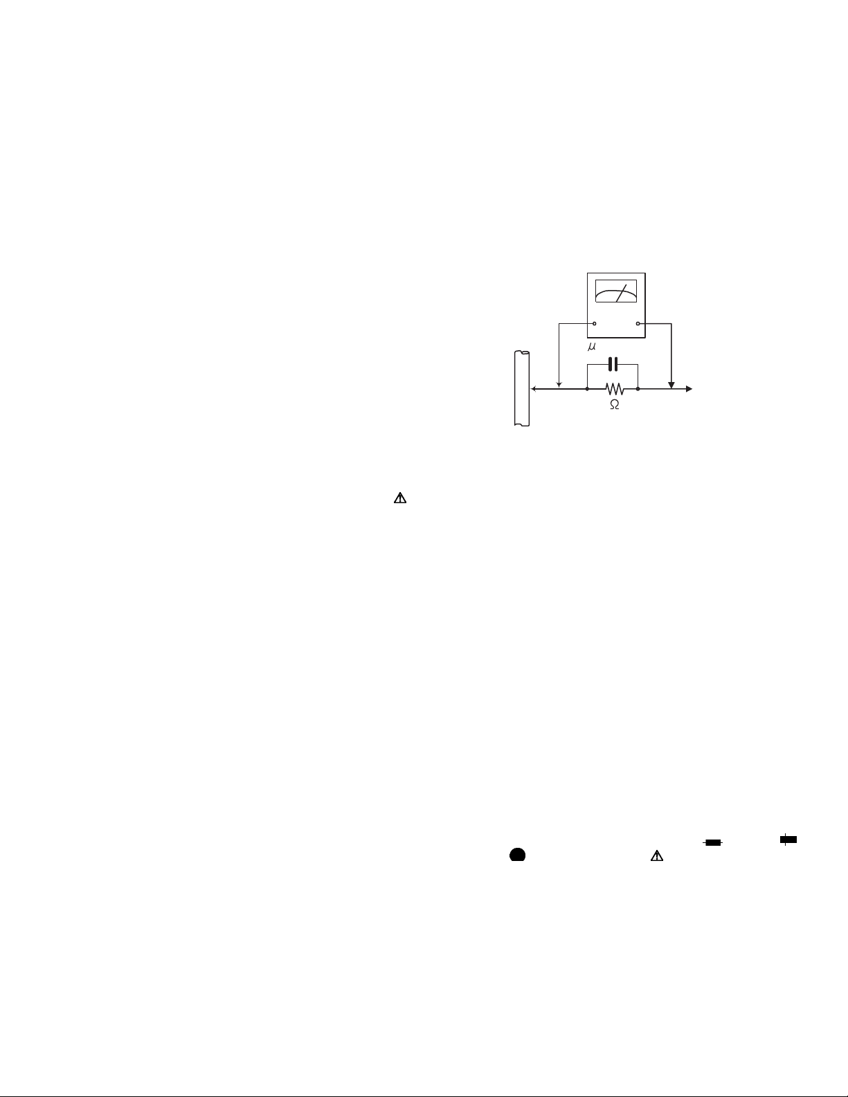
(5) Leakage shock hazard testing
After reassembling the product, always perform an isolation check on the exposed metal parts of the product (antenna terminals, knobs, metal cabinet, screw heads,
headphone jack, control shafts, etc.) to be sure the product
is safe to operate without danger of electrical shock.Do not
use a line isolation transformer during this check.
• Plug the AC line cord directly into the AC outlet. Using a
"Leakage Current Tester", measure the leakage current
from each exposed metal parts of the cabinet, particularly any exposed metal part having a return path to the
chassis, to a known good earth ground. Any leakage current must not exceed 0.5mA AC (r.m.s.).
• Alternate check method
Plug the AC line cord directly into the AC outlet. Use an
AC voltmeter having, 1,000Ω per volt or more sensitivity
in the following manner. Connect a 1,500Ω 10W resistor
paralleled by a 0.15µF AC-type capacitor between an ex-
posed metal part and a known good earth ground.
Measure the AC voltage across the resistor with the AC
voltmeter.
Move the resistor connection to each exposed metal
part, particularly any exposed metal part having a return
path to the chassis, and measure the AC voltage across
the resistor. Now, reverse the plug in the AC outlet and
repeat each measurement. Voltage measured any must
not exceed 0.75 V AC (r.m.s.). This corresponds to 0.5
mA AC (r.m.s.).
AC VOLTMETER
(Having 1000
ohms/volts,
or more sensitivity)
0.15 F AC TYPE
Place this
probe on
1500 10W
Good earth ground
1.2 Warning
(1) This equipment has been designed and manufactured to
meet international safety standards.
(2) It is the legal responsibility of the repairer to ensure that
these safety standards are maintained.
(3) Repairs must be made in accordance with the relevant
safety standards.
(4) It is essential that safety critical components are replaced
by approved parts.
(5) If mains voltage selector is provided, check setting for local
voltage.
1.3 Caution
Burrs formed during molding may be left over on some parts
of the chassis.
Therefore, pay attention to such burrs in the case of preforming repair of this system.
1.4 Critical parts for safety
In regard with component parts appearing on the silk-screen
printed side (parts side) of the PWB diagrams, the parts that are
printed over with black such as the resistor ( ), diode ( )
and ICP ( ) or identified by the " " mark nearby are critical
for safety. When replacing them, be sure to use the parts of the
same type and rating as specified by the manufacturer.
(This regulation dose not Except the J and C version)
each exposed
metal part.
(No.MB196)1-3
Page 4
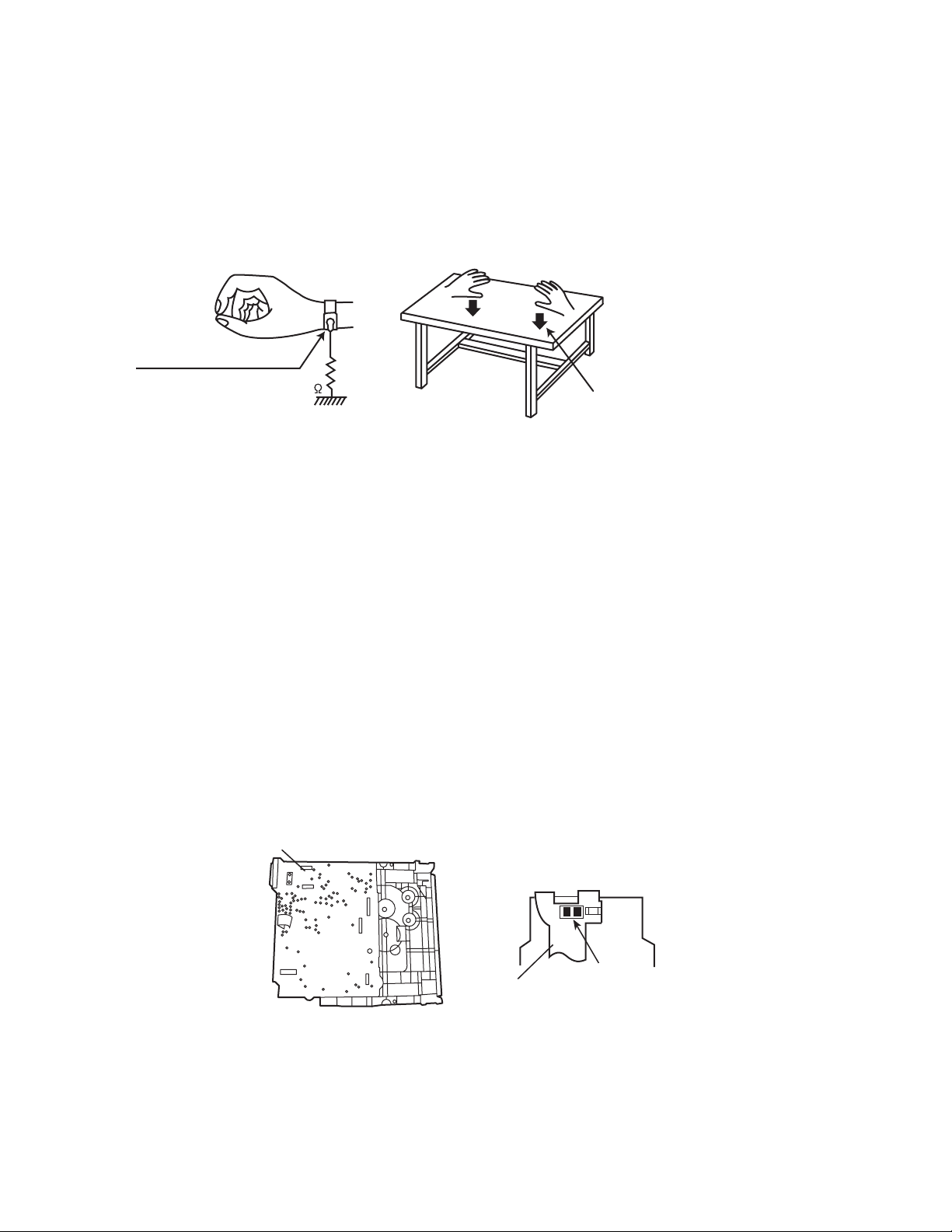
1.5 Preventing static electricity
Electrostatic discharge (ESD), which occurs when static electricity stored in the body, fabric, etc. is discharged, can destroy the laser
diode in the traverse unit (optical pickup). Take care to prevent this when performing repairs.
1.5.1 Grounding to prevent damage by static electricity
Static electricity in the work area can destroy the optical pickup (laser diode) in devices such as laser products.
Be careful to use proper grounding in the area where repairs are being performed.
(1) Ground the workbench
Ground the workbench by laying conductive material (such as a conductive sheet) or an iron plate over it before placing the
traverse unit (optical pickup) on it.
(2) Ground yourself
Use an anti-static wrist strap to release any static electricity built up in your body.
(caption)
Anti-static wrist strap
1M
Conductive material
(conductive sheet) or iron palate
(3) Handling the optical pickup
• In order to maintain quality during transport and before installation, both sides of the laser diode on the replacement optical
pickup are shorted. After replacement, return the shorted parts to their original condition.
(Refer to the text.)
• Do not use a tester to check the condition of the laser diode in the optical pickup. The tester's internal power source can easily
destroy the laser diode.
1.6 Handling the traverse unit (optical pickup)
(1) Do not subject the traverse unit (optical pickup) to strong shocks, as it is a sensitive, complex unit.
(2) Cut off the shorted part of the flexible cable using nippers, etc. after replacing the optical pickup. For specific details, refer to the
replacement procedure in the text. Remove the anti-static pin when replacing the traverse unit. Be careful not to take too long a
time when attaching it to the connector.
(3) Handle the flexible cable carefully as it may break when subjected to strong force.
(4) I t is not possible to adjust the semi-fixed resistor that adjusts the laser power. Do not turn it.
1.7 Attention when traverse unit is decomposed
*Please refer to "Disassembly method" in the text for the pickup unit.
• Apply solder to the short land sections before the flexible wire is disconnected from the connecto on the servo board. (If the flexible
wire is disconnected without applying solder, the pickup may be destroyed by static electricity.)
• In the assembly, be sure to remove solder from the short land sections after connecting the flexible wire.
CD changer
unit
1-4 (No.MB196)
Flexible cable
Soldering
Page 5
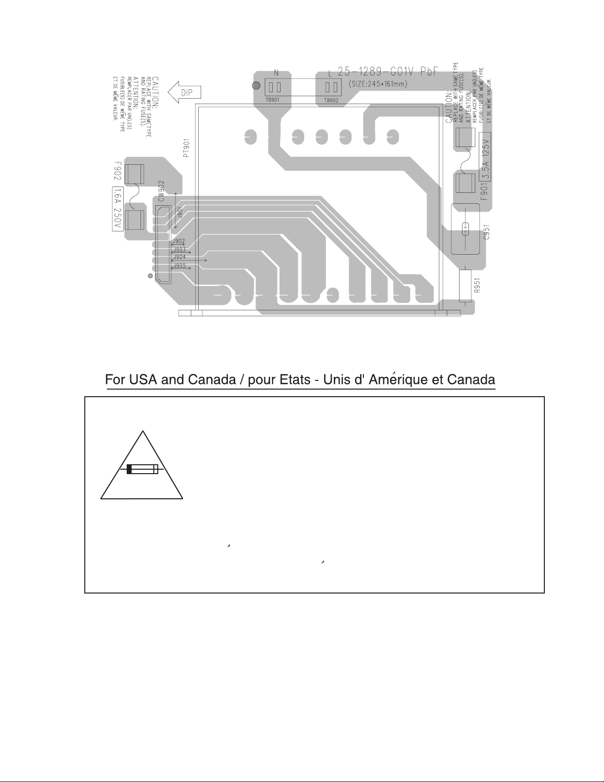
1.8 Importance administering point on the safety
Caution: For continued protection against risk of
fire, replace only with same type 3.5A/125V for
F901 and 1.6A/250V for F902.
This symbol specifies type of fast operating fuse.
Precaution: Pour eviter risques de feux, remplacez
le fusible de surete de F901 comme le meme type
que 3.5A/125V et 1.6A/250V pour F902.
Ce sont des fusibles suretes qui functionnes rapide.
^
(No.MB196)1-5
Page 6

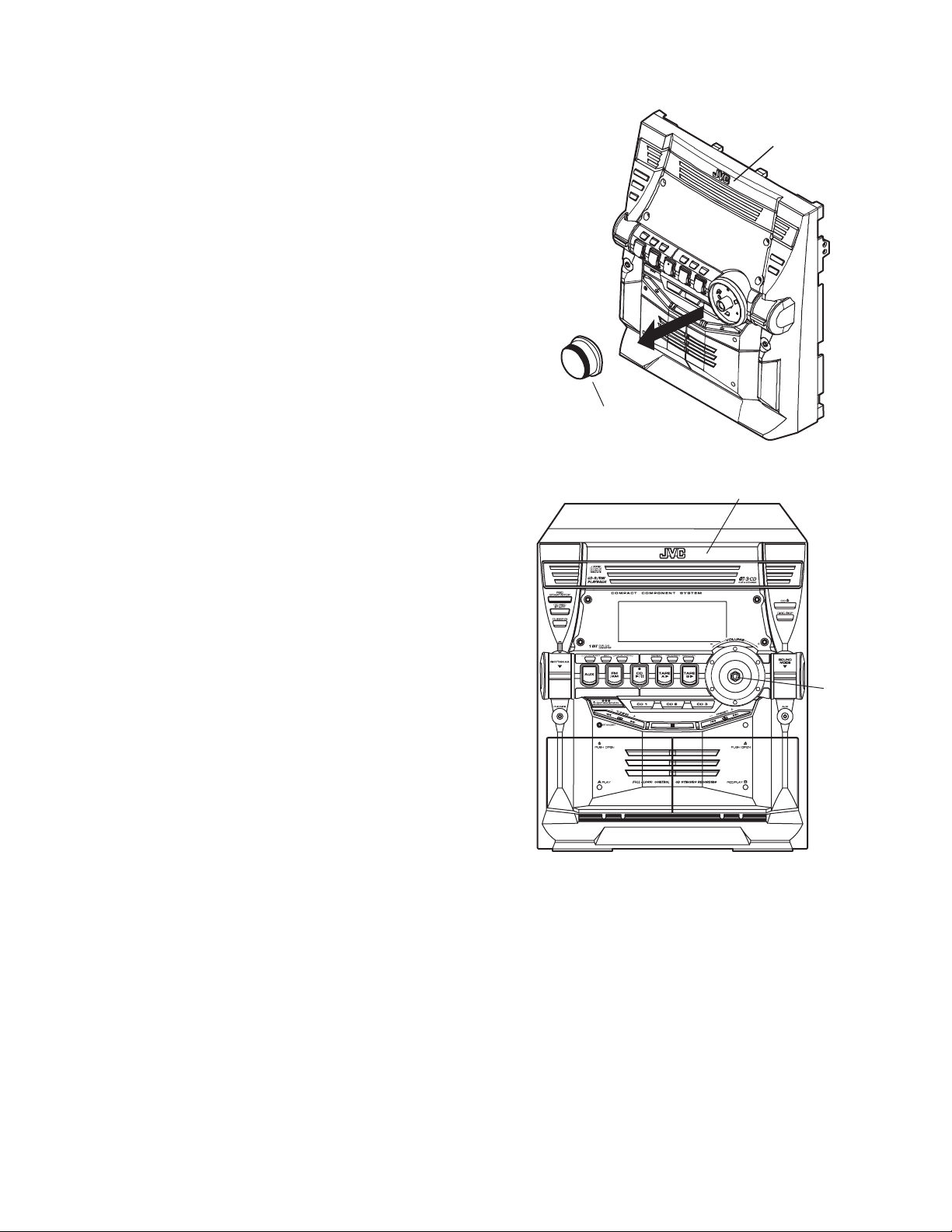
SECTION 2
SPECIFIC SERVICE INSTRUCTIONS
This service manual does not describe SPECIFIC SERVICE INSTRUCTIONS.
1-6 (No.MB196)
Page 7
SECTION 3
DISASSEMBLY
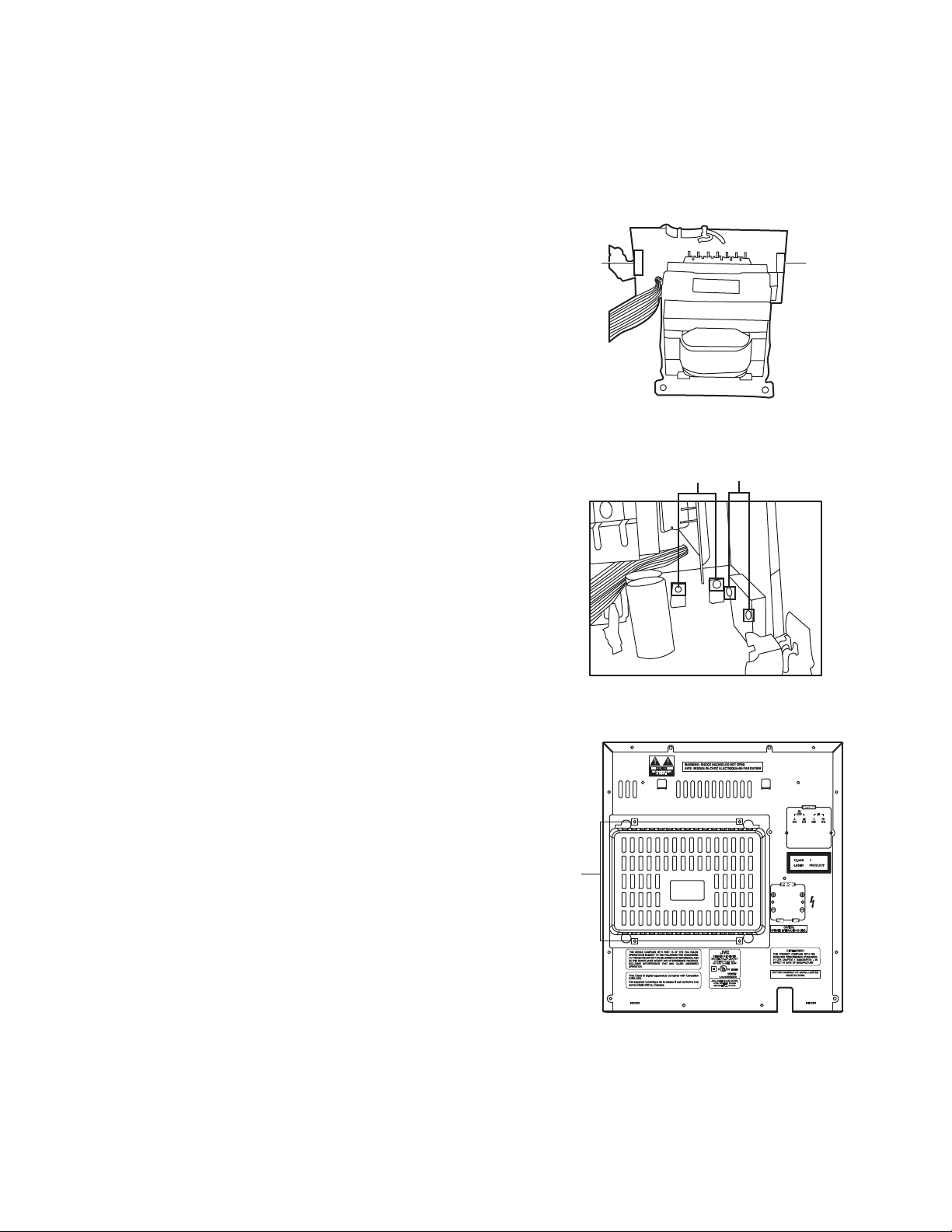
3.1 Disassembly of the main blocks of the set
Replacement of the fuses and the power IC
3.1.1 Replacing the fuses
(See Fig.1)
• Prior to performing the following procedure, remove the left
side board.
(1) Replace the fuses inside.
Caution:
Be sure to use fuses with the specified ratings.
3.1.2 Replacing the power IC
(See Fig.2)
• Prior to performing the following procedure, remove the top
cover.
(1) Remove the two screws A from the heat sink between the
power IC.
(2) Remove the solder fixing the power IC.
Fuse (F902)
1.6A 250V
Fig.1
W
Fuse (F901)
3.5A 125V
A
3.1.3 Replacing the heat sink cover
(See Fig.3)
(1) Remove four screws B from the rear panel.
(2) Pull the heat sink cover outward.
Fig.2
B
Fig.3
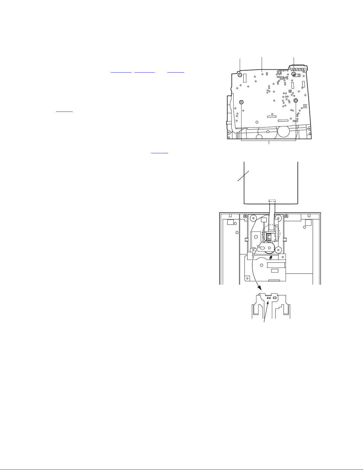
(No.MB196)1-7
Page 8
3.1.4 Removing the top cover
(See Fig.4 and 5)
(1) Remove six screws C that retain the top cover from the
panel rear of the body.
(2) Remove six screws D that retain the top cover from the two
sides of the body.
(3) Remove the top cover from the body by lifting it toward the
rear.
Top cover
C
CC
Fig.4
Right Front panel assembly
D
D
Left Front panel assembly
D
D
Fig.5
1-8 (No.MB196)
Page 9
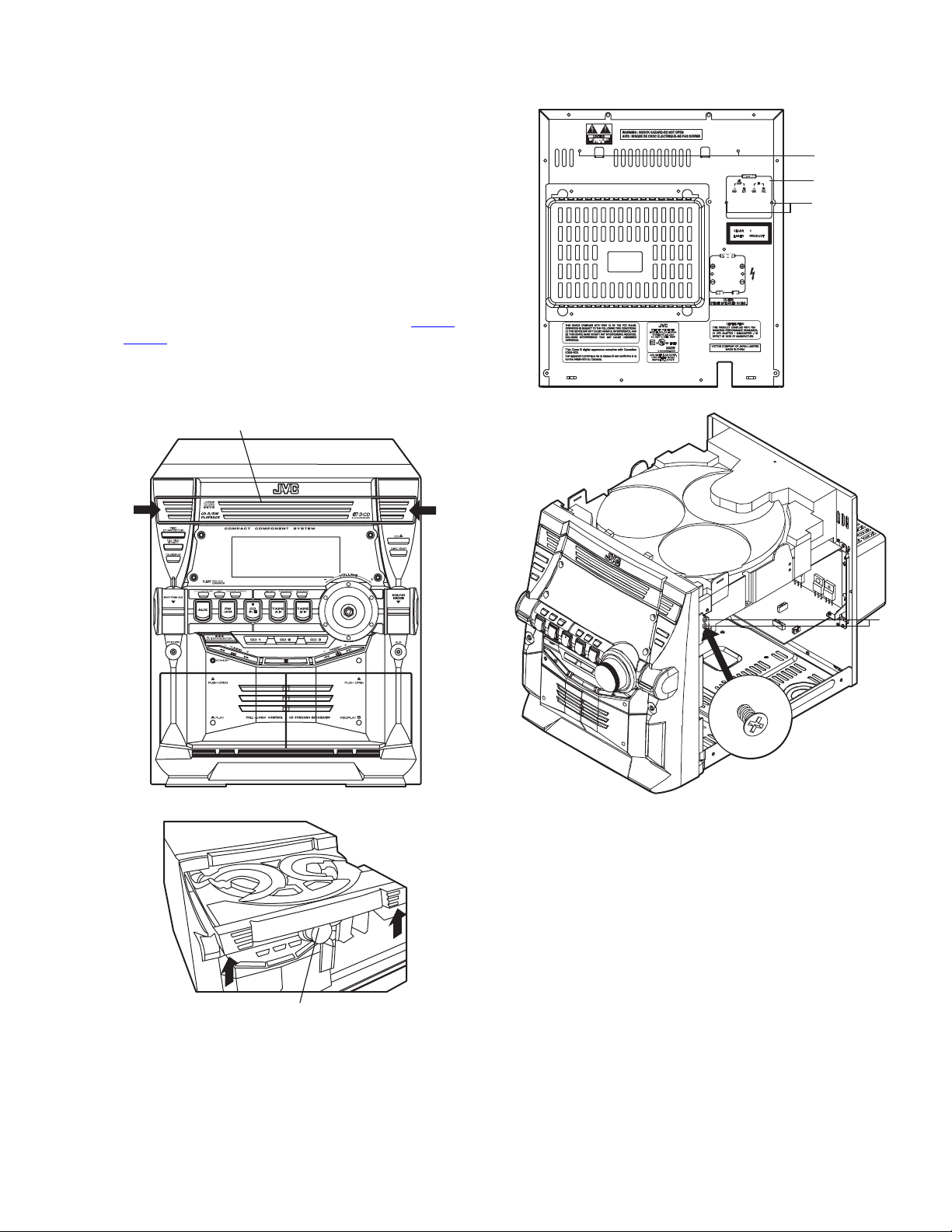
3.1.5 Removing the CD changer unit
(See Fig.6 to 9)
• Prior to performing the following procedures, remove the top
cover.
Caution:
Although the CD mechanism unit can be removed without removing the CD tray panel, it is still recommended to remove it
in order to prevent damage.
a. From the front panel side of this set, push in the sections
marked with arrows and pull out the CD tray toward the
front.
b. Remove the CD tray panel by pushing both of its extremi-
ties upward in the direction of the arrows.
c. Push the CD tray deep into the set.
(1) Disconnect the cord wires from the CD board CN703
.
CN203
and
(2) From the rear of the set, remove two screws E, two screws
F and four screws G on the front panel left and right side.
(3) Handle the CD changer unit rear, take out the unit.
CD tray panel
E
Antenna
terminal
F
Fig.8
Fig.6
CD tray panel
Fig.7
G
Fig.9
(No.MB196)1-9
Page 10
3.1.6 Removing the front panel assembly
(See Fig.10 to 11)
• Prior to performing the following procedures, remove the top
cover.
• Also remove the CD changer unit.
(1) Disconnect the parallel wire and the cord wire from the con-
nectors CN701
(2) Remove one screws H retaining the front panel assembly
onto the bottom of the body.
(3) Remove two screws I on the left and right side of the set re-
taining the panel front from the bottom and then remove
then GND lug b that comes from the amp and supply
board.
(4) Disengage the claws c on both sides of the front panel as-
sembly and then remove the assembly.
, CN101 on the power amp. PCB.
H
Fig.10
a
Fig.11
GND lugGND lug
b
Claw
c
1-10 (No.MB196)
Page 11
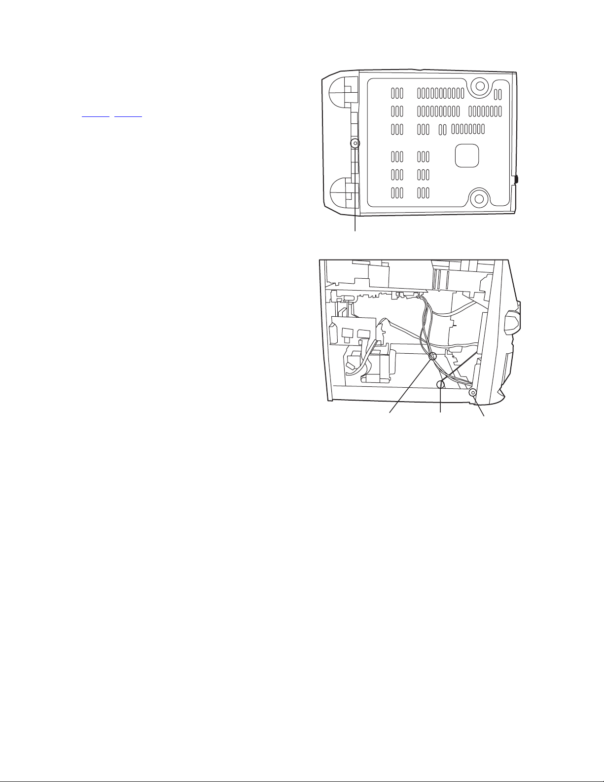
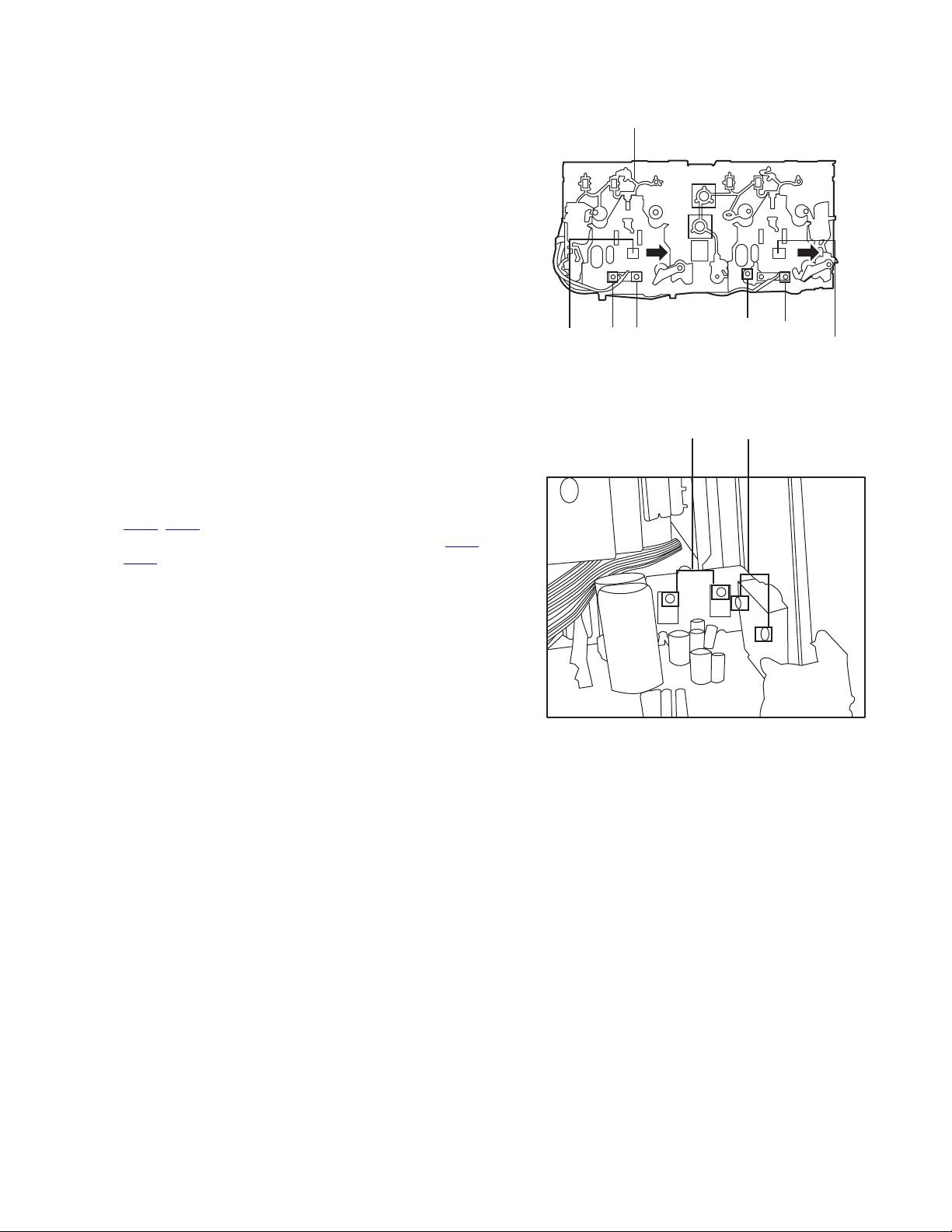
3.2 Disassembly of units and assembly inside this set
3.2.1 Removing the Main board
(See Fig.12 to 13)
• Prior to performing the following procedures, remove the top
cover.
• Also remove the CD changer unit.
(1) Disconnect the wires from CN603A
on the Main board, which is located on the back side of the
CD changer unit.
(2) The four screws J that retain the CD board should be re-
moved.
(3) Remove the CD board by pulling it toward the side where
the CN601
(4) Using solder, short the CD pickup to connect to short
round.
Caution:
After re-connecting the wires, be sure to remove the
shorting solder from the GND connection.
(5) Disconnect the card wire from the connector CN601
Main board and then remove the Main board.
is located.
, CN603B and CN604
on the
CD PCB
J
PAIN PCB
J
Fig.12
CN601
J
Short round
Fig.13
(No.MB196)1-11
Page 12
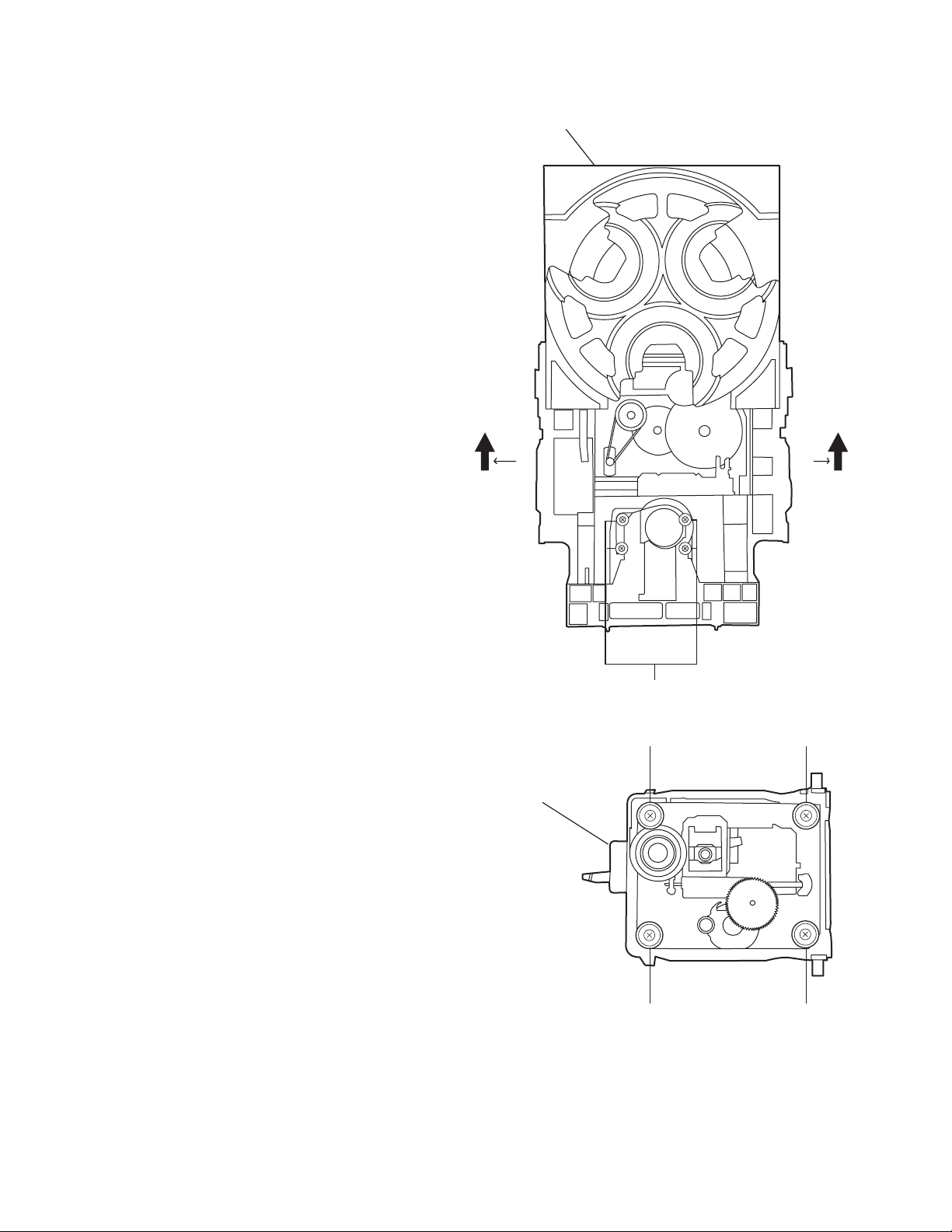
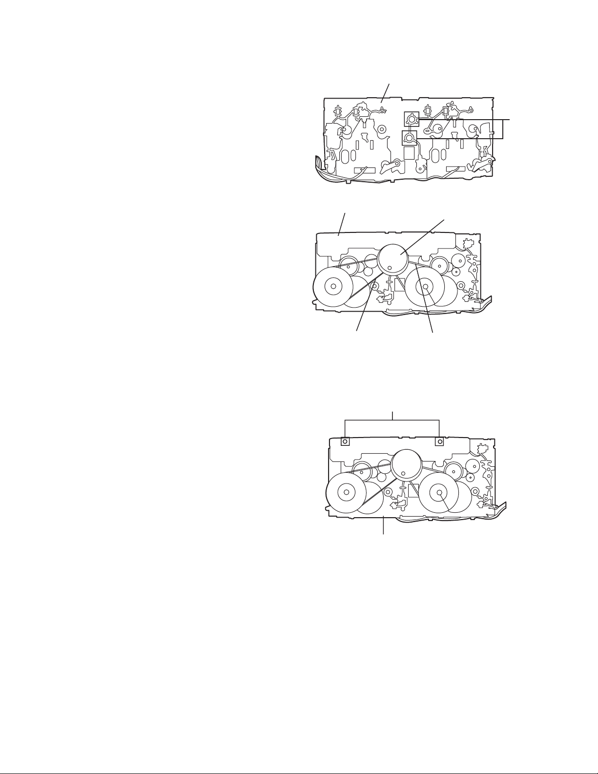
3.2.2 Removing the CD changer mechanism assembly
(See Fig.14 to 15)
• Also remove the CD changer unit.
(1) Turn the CD changer mechanism cover base and remove
the screws d connecting the unit to the CD changer mechanism assembly.
(2) Removing four screws e retaining the CD mechanism hold-
er assembly.
Caution:
When replacing the CD changer mechanism assembly, be
sure not to mistake the positions of the silver color and copper
color spring.
CD changer
unit
CD changer
mechanism
assembly
d
Fig.14
e
( Green color )
e
( Green color )
Fig.15
e
( Red color )
e
( Red color )
1-12 (No.MB196)
Page 13
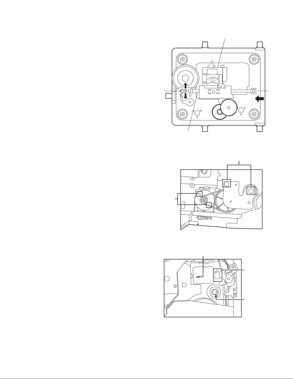
3.2.3 Removing the CD pickup
r
(See Fig.16)
• Prior to performing the following procedures, remove the top
cover.
• Also remove the CD changer unit.
• Also remove the CD changer mechanism.
(1) Widen the section f.
(2) While keeping the section f wide open, push the section g
in the direction of the arrow to remove the shaft, and then
remove the CD pickup.
CD pickup
f
3.2.4 Replacing the loading motor and rotor belt of the CD changer
(See Fig .17)
• Prior to performing the following procedures, remove the top
cover.
• Also open the CD changer tray.
(1) Remove the two screws L retaining the CD changer tray
loading motor.
(2) Remove the two screws M retaining the gear plate and take
it out, after remove the rotor belt from the pulley.
g
Shaft
Fig.16
M
L
3.2.5 Replacing the CD turn table and removing the motor
(See Fig.18 )
• Prior to performing the following procedures, remove the top
cover.
• Also remove the CD changer unit.
(1) Remove the one screws retaining the CD (Turn table).
(2) Remove the two screws retaining the stopper brackets on
both sides of the CD changer unit.
(3) Remove the stopper brackets from both sides of the CD
changer unit.
(4) Pull out the CD tray from the CD changer unit, all the way
and lift the tray to remove.
(5) Remove the gear and after push out the tray motor locker
and pull out the tray motor from the CD tray.
Fig.17
Turn table motor
Motor locker
Obligue gea
Fig.18
(No.MB196)1-13
Page 14
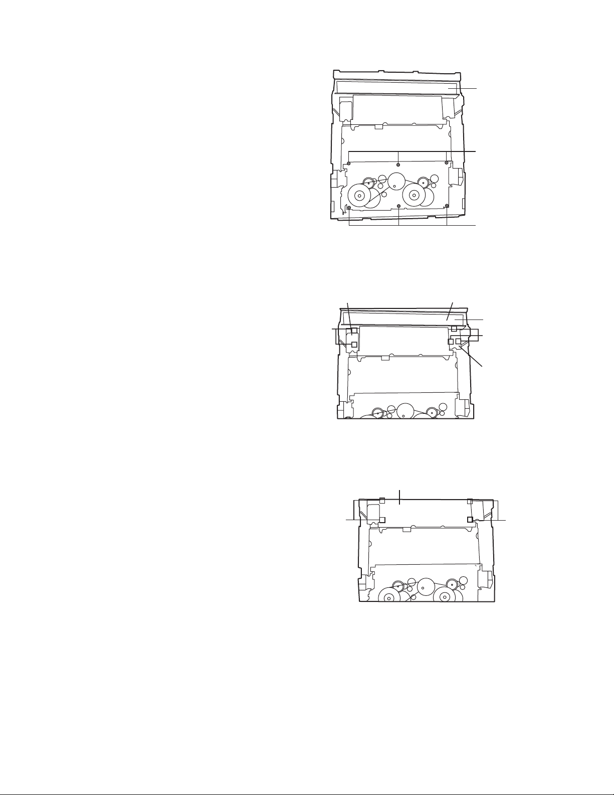
3.2.6 Removing the cassette deck mechanism
(See Fig.19)
• Prior to performing the following procedures, remove the top
cover.
• Also remove the CD changer unit.
• Also remove the front panel assembly.
(1) Remove six screws Z retaining the cassette deck mecha-
nism.
3.2.7 Removing the Key open board & the Key rec board
(See Fig.20)
• Prior to performing the following procedures, remove the top
cover.
• Also remove the CD changer unit.
• Also remove the front panel assembly.
(1) Remove two screws P that retains the Key open board.
(2) Remove three screws L that retains the Key REC board.
Key open
board
P
Front panel
assembly
Z
Z
Fig.19
Front panel
assembly
Front panel
assembly
L
3.2.8 Removing the Display board
(See Fig.21)
• Also remove the CD changer unit.
• Also remove the front panel assembly.
(1) Remove six screws Q that retain the Display board from the
back of the front panel unit.
Key REC
board
Fig.20
Display
PCB
Q
Fig.21
Q
1-14 (No.MB196)
Page 15
3.2.9 Removing the Switch board and sound mode and CD function switch board
y
(See Fig.20 to 23)
• Prior to performing the following procedures, remove the top
cover.
• Also remove the CD changer unit.
• Also remove the front panel assembly.
(1) Pull out the volume control knob from the front of the front
panel assembly.(Fig.22)
(2) Remove six screws Q retaining the front panel assembly.
(3) Remove the Control/FL board.
(4) Remove eleven screws retaining the Switch (key 1)
board.(Fig.20)
(5) Remove two screws S retaining the sound mode and CD
function (key 2) switch board.(Fig.21)
Volume knob
Front panel assembl
Fig.22
Front panel
assembly
Volume
shaft
Fig.23
(No.MB196)1-15
Page 16
3.2.10 Removing the cassette deck main motor, and replacing the main belts
r
(See Fig.19, 24 and 25)
• Prior to performing the following procedures, remove the top
cover and both sides board.
• Also remove the CD changer unit.
• Also remove the front panel assembly.
(1) Remove six screws Z retaining the cassette deck mecha-
nism. (Fig.19)
(2) Remove the cassette deck mechanism.
(3) Remove two screws t retaining the main motor from the
front side of the cassette deck.
Caution:
After attaching the main motor, check the orientation of
the motor and the polarity of the wires.
(4) From the backside of the cassette deck, remove the main
motor and two main belts.
Caution:
The lengths of the cassette A(playback only) and cassette B(record/play) main belts are different. When attaching the main belts, use the longer belt for cassette A.
Cassette deck mechanism
(Back side)
Cassette deck mechanism
(Front side)
t
Fig.24
Cassette deck main moto
3.2.11 Removing the leaf switches of the cassette deck mechanism
(See Fig. 19 and 26)
• Prior to performing the following procedures, remove the top
cover and both sides board.
• Also remove the CD changer unit.
• Also remove the front panel assembly.
(1) Remove the six screws Z that retain the cassette deck
mechanism. (Fig.19)
(2) Remove the cassette deck mechanism.
(3) Turn the cassette deck mechanism upside down.
(4) Remove the solder from around the leaf switches.
(5) Pull out the leaf switches from the front side of the cassette
deck mechanism.
Main belt
(For B cassette)
Fig.25
Solder side of leaf switch
Cassette deck mechanism
Fig.26
Main belt
(For A cassette)
(Back side)
1-16 (No.MB196)
Page 17
3.2.12 Removing the cassette deck heads
(See Fig. 19 and 27)
• Prior to performing the following procedures, remove the top
cover and both sides board.
• Also remove the CD changer unit.
• Also remove the front panel assembly.
(1) Remove six screws Z that retain the cassette deck mecha-
nism. (Fig.19)
(2) Remove the cassette deck mechanism and place it so that
the front side faces up.
(3) Remove the solder from the bottom side of the head termi-
nal and disconnect the wire.
(4) Remove screws U that retains the head.
(5) Remove screws V that retains the head.
(6) Hold the head and slide it in the direction of the arrow to re-
move it.
3.2.13 Removing the 3-pin regulator and bridge diode
(See Fig. 28)
• Prior to performing the following procedures, remove the top
cover and both sides board.
Remove two screws A that connect the heat sink.
(1) Remove two screws A that connect the heat sink.
(2) Remove two screws W that connect the heat sink.
(3) Remove the solder fixing the the 3-pin terminal regulator
, Q608.
Q604
(4) Remove the solder fixing the 4-pin bridge diode (D614
D615).
PB Head
Cassette deck mechanism
(Front side)
V
U
VU
REC/PB Head
Fig.27
W
A
,
Fig.28
(No.MB196)1-17
Page 18

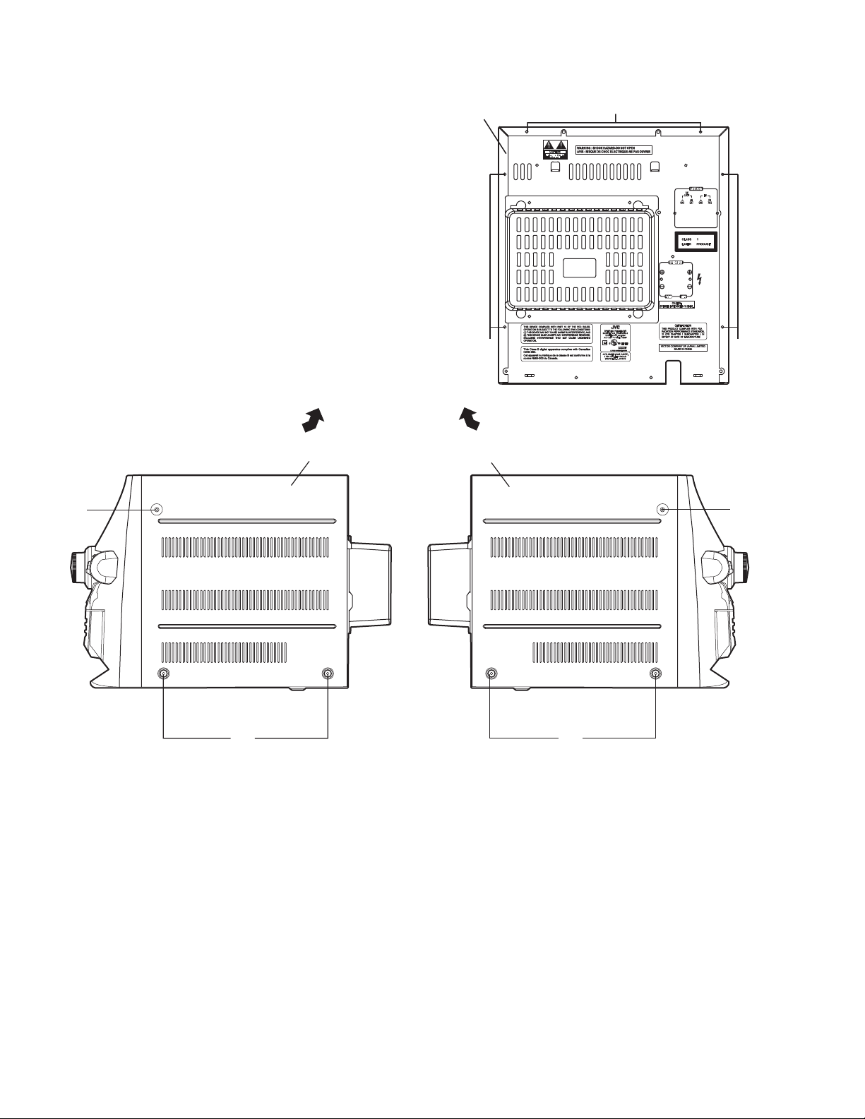
3.2.14 Removing the Power amp and Supply board and the Power trans board
A
(See Fig. 3, 29 to 31)
• Prior to performing the following procedures, remove the top
cover and CD changer unit.
(1) Remove four screws B from the rear panel. (Fig.3)
(2) Pull the heat sink cover outward.
(3) Remove four screws AA from the rear panel between the
heat sink holder.
(4) Remove four screws YY that retains the rear panel, and
then remove the rear panel.
(5) Disconnect the parallel wires from the connectors FW951
on the Power trans board.
(6) Remove screws Z that retain the Power amp and Supply
board and then remove the assembly.
(7) Remove the clamp of AC power cord from the chassis.
(8) Remove four screws that retain the Power trans board and
then remove the assembly.
Fuse (F902)
1.6A 250V
A
Fuse (F901)
3.5A 125V
Fig.29
Rear panel
YY
Fig.30
Power amp and
supply board
Chassis
Z
Fig.31
Clamp
1-18 (No.MB196)
Page 19

SECTION 4
ADJUSTMENT
4.1 Measurement Instruments Required for Adjustment
(1) Low frequency oscillator
This oscillator should have a capacity to output 0dBs to
600Ω at an oscillation frequency of 50Hz-20kHz.
(2) Attenuator impedance : 600Ω
(3) Electronic voltmeter
(4) Frequency counter
(5) Wow & flutter meter
(6) Test tape
VT712 : For Tape speed and wow flutter ( 3kHz)
VT703 : For Head angle (10kHz)
(7) Blank tape
TYPE l : AC-225
TYPE ll : AC-514
(8) Torque gauge
For play and back tension forward; TW2111A
Reverse; TW2121A
Fast Forward and Rewind; TW2231A
(9) Test disc
CTS-1000(12cm)
GRG-1211(8cm)
(10) Jitter meter
4.2 Measurement conditons
Power supply voltage AC 120V ~, 60Hz
Measurement
output terminal
4.2.1 Radio Input signal
AM modulation frequency 400Hz
Modulation factor 30%
FM modulation frequency 1 kHz
Frequency displacement 22.5kHz
Speaker out
TP101
(Measuring for TUNER/ DECK/CD)
Dummy load 6Ω
4.2.2 Standard measurement position of volume and
switch
Power Standby
(Light STANDBY Indicator)
Sound Turbo,A,BASS EX OFF
Sound mode OFF
Main VOL. 0 Minimum
Travers mecha set position Disc 1
Precautions for measurement
(1) Apply 30pF and 33kΩ to the IF sweeper output side and
0.082µ F and 100kΩ in series to the sweeper input side.
(2) The IF sweeper output level should be made as low as
possible within the adjustable range.
(3) Since the IF sweeper is a fixed device, there is no need
to adjust this sweeper.
(4) Since a ceramic oscillator is used, there is no need to
perform any MIX adjustment.
(5) Since a fixed coil is used, there is no need to adjust the
FM tracking.
(6) The input and output earth systems are separated. In
case of simultaneously measuring the voltage in both of
the input and output systems with an electronic voltmeter
for two channels, therefore, the earth should be connected particularly carefully.
(7) In the case of BTL connection amp., the minus terminal
of speaker is not for earthing. Therefore, be sure not to
connect any other earth terminal to this terminal. This
system is of an BTL system.
(8) For connecting a dummy resistor when measuring the
output, use the wire with a greater code size.
(9) Whenever any mixed tape is used, use the band pass fil-
ter (DV-12).
(No.MB196)1-19
Page 20

4.3 Arrangement of adjusting positions
Cassette deck mechanism
(Front side)
4.3.1 Tape recorder section
Items
Cassette Head
Azimuth Alignments
Measurement
conditions
Test tape
: VT703 (10kHz)
Measurement output
terminal
: Left and Right
speaker output
(6-ohm loaded)
or
Headphone Output
(32-ohm loaded)
PB Head
(Deck-A)
Head azimuth screw
(Forward side)
Head azimuth screw
1. Playback the test tape VT703 (10KHz) or equivalent.
2. Adjust the head azimuth screw to obtain maximum
output and both output of L / R is in 3dB.
3. Put on the screw lock paint after alignments.
Head azimuth screw
(Forward side)
(Reverse side)
Measurement method
REC/PB Head
(Deck-B)
Head azimuth screw
(Reverse side)
Standard
values
Maximum output
Adjusting
positions
Adjust the
head azimuth
screw only
when the head
has been
changed.
Recording Bias
Frequency Alignment
Test tape
: TYPE AC-514
Measurement output
terminal
1. Insert the recording tape in deck-B.
2. Starting the recording.
3. Adjust the oscillation frequency to 80KHz+/-3KHz by
core of Oscillation coil of L301.
: Erase head terminal
(CN308 8-Pin)
4.3.2 Tuner section
Items
AM Tracking
Alignments
Measurement
conditions
Input signal
: 530kHz
600kHz
Adjustment point
: Antenna coil (L2)
1. Set the Signal Generator signal to 530KHz the feed
to Loop Antenna.
2. Receiving the signal and the adjust the OSC coil (L2)
obtain the V.T is 1.40V +/-0.05V.
3. Change the receiving frequency to 600KHz (603KHz).
4. Adjust the Antenna coil ( L2 ) obtain maximum
sensitivity. (Adjust the SSG output to out of AGC range.)
AM IFT Alignments
Input signal
: 530kHz
Adjustment point
: IFT (T1)
1. Set the receiving frequency to 530KHz.
2. Feed the 450KHz signal to AM antenna input.
3.Adjust the IFT Block T1 obtain to maximum output.
(Adjust the SSG output to out of AGC range.)
Note: The adjustment of CD section is not required.
Measurement method
80kHz+/-3kHz
Standard
values
V. T
: 1.40V+/-0.05V
Maximum
sensitivity
Maximum output
Use the HighImpedance
Probe or
Frequency
counter input.
Adjusting
positions
Adjust the OSC
coil only when
the AM coil block
has been changed.
Adjust the IFT
only when the
IFT block has
been changed.
1-20 (No.MB196)
Page 21

TROUBLESHOOTING
5.1 Flow of functional operation until TOC read
Power ON
Play Key
SECTION 5
Slider turns REST
SW ON.
Automatic tuning
of TE offset
Check Point
Confirm that the voltage at the pin5
of CN702 is "H"\"L"\"H".
Tracking error waveform at TOC reading
Approx.3sec
Tracking
servo
off states
Automatic measurement
of TE amplitude and
automatic tuning of
TE balance
VREF
pin 20 of
IC611(TE)
Approx
0.3V
Disc states
to rotate
Tracking
servo
on states
Disc to be
braked to stop
TOC reading
finishes
500mv/div
2ms/div
Fig-1
Laser ON
Detection of disc
Automatic tuning of
Focus offset
Automatic measurement of
Focus S-curve amplitude
Disc is rotated
Focus servo ON
(Tracking servo ON)
Automatic measurement of
Tracking error amplitude
Automatic tuning of
Tracking error balance
Check that the voltage at the
pin10 of IC701 is + 0V?
Confirm that the Focus error
S-cuve signal at the pin31 of
IC701 is approx.2Vp-p
Confirm that the signal from
pin26 IC701 is 0V as a
accelerated pulse during
approx.400ms.
Confirm the waveform of
the Tracking error signal.
at the pin 29 of IC701 (R729)
(See fig-1)
Automatic tuning of
Focus error balance
Automatic tuning of
Focus error gain
Automatic tuning of
Tracking error gain
TOC reading
Play a disc
Confirm the eys-pattern
at the lead of Pin 2 of IC 701
(No.MB196)1-21
Page 22

5.2 Maintenance of laser pickup
(1) Cleaning the pick up lens
Before you replace the pick up, please try to clean the lens
with a alcohol soaked cotton swab.
(2) Life of the laser diode
When the life of the laser diode has expired, the following
symptoms will appear.
• The level of RF output (EFM output : ampli tude of eye
pattern) will below.
5.3 Replacement of laser pickup
Turn off the power switch and,disconnect the
power cord from the AC OUTLET.
Replace the pickup with a normal one.(Refer
to "Pickup Removal" on the previous page)
Is the level of
RFOUT under
0.48V 0.1Vp-p?
NO
Replace it.
YES
O.K
(3) Semi-fixed resistor on the APC PC board
The semi-fixed resistor on the APC printed circuit board
which is attached to the pickup is used to adjust the laser
power. Since this adjustment should be performed to
match the characteristics of the whole optical block, do not
touch the semi-fixed resistor.
If the laser power is lower than the specified value, the laser diode is almost worn out, and the laser pickup should
be replaced.
If the semi-fixed resistor is adjusted while the pickup is
functioning normally, the laser pickup may be damaged
due to excessive current.
Plug the power cord in,and turn the power on.
At this time,check that the laser emits for
about 3seconds and the objective lens moves
up and down.
Note: Do not observe the laser beam directly.
Play a disc.
Check the eye-pattern at
Pin 2 of IC 701
Finish.
1-22 (No.MB196)
Page 23

(No.MB196)1-23
Page 24

VICTOR COMPANY OF JAPAN, LIMITED
AV & MULTIMEDIA COMPANY AUDIO/VIDEO SYSTEMS CATEGORY 10-1,1chome,Ohwatari-machi,Maebashi-city,371-8543,Japan
(No.MB196)
Printed in Japan
WPC
Page 25

SCHEMATIC DIAGRAMS
COMPACT COMPONENT SYSTEM
MX-KB4
CD-ROM No.SML200406
STANDBY/ON
SLEEP
AUX
FM /AM
FM MODE
CD
CD1CD2CD
3
PROGRAM/RANDOM
REPEAT
TAPE
TAPE
A
B
SOUND
VOLUME
MODE
FADE
MUTING
RHYTHM AX
REMOTE CONTROL
CA-MXKB4SP-MXKB4 SP-MXKB4
Area suffix
J ---------------------------- U.S.A.
C ------------------------- Canada
Contents
Wiring diagram ------------------------------------------------------ 2-1
Block diagram -------------------------------------------------------- 2-2
Standard schematic diagrams ----------------------------------- 2-3
Printed circuit boards --------------------------------------- 2-9 to 13
COPYRIGHT 2004 VICTOR COMPANY OF JAPAN, LTD.
No.MB196SCH
2004/6
Page 26

In regard with component parts appearing on the silk-screen printed side (parts side) of
the PWB diagrams, the parts that are printed over with black such as the resistor ( ),
diode ( ) and ICP ( ) or identified by the " " mark nearby are critical for safety.
(This regulation does not correspond to J and C version.)
Page 27

Wiring diagram
2-1
Page 28

Block diagrams
2-2
Page 29

Standard schematic diagrams
Main amp. / Power supply section
Parts are safety assurance parts.
When replacing those parts make
sure to use the specified one.
2-3
Page 30

Function control section
2-4
Page 31

System control section
2-5
Page 32

FL / Key control section
2-6
Page 33

CD / MP3 control section
2-7
Page 34

Tuner section
2-8
Page 35

Printed circuit boards
Main board (forward side)
2-9
Page 36

Main board (reverse side)
2-10
Page 37

Front board (forward side)
2-11
Page 38

Front board (reverse side)
2-12
Page 39

Amp board (forward side) Amp board (reverse side)
2-13
Page 40

Power trans board
2-14
Page 41

< MEMO >
Page 42

VICTOR COMPANY OF JAPAN, LIMITED
AV & MULTIMEDIA COMPANY AUDIO/VIDEO SYSTEMS CATEGORY 10-1,1chome,Ohwatari-machi,Maebashi-city,371-8543,Japan
(No.MB196SCH)
Printed in Japan
WPC
Page 43

PARTS LIST
[ MX-KB4 ]
* All printed circuit boards and its assemblies are not available as service parts.
Area suffix
J ----------------------------- U.S.A.
C -------------------------- Canada
MB196
- Contents -
Exploded view of general assembly and parts list (Block No.M1)
CD changer mechanism assembly and parts list (Block No.MA)
Cassette mechanism assembly and parts list (Block No.MP)
Electrical parts list (Block No.01~04)
Packing materials and accessories parts list (Block No.M3)
3- 2
3- 5
3- 7
3- 9
3-12
- Note-
Parts number of normal capacitors and normal resistors doesn't listed on the parts list
3-1
Page 44

Exploded view of general assembly and parts list
o
Block No.
46
M
1
47
M
M
39
17
16
50
50
49
48
50
Front b
CD door board
35
51
38
41
40
37
42
2
1
3
9
6
48
31
36
34
VFD board
50
32
30
15
51
11
12
13
10
3-2
4
7
8
5
Page 45

27
46
8
board
Main board
49
48
45
Amp. board
47
46
47
21
43
25
22
23
46
48
47
46
48
24
46
14
F902
18
F901
19
44
Power trans. board
46
3-3
Page 46

General Assembly
Symbol No. Part No. Part Name Description Local
1 BI1077280101U1 COVER CASS L HIPS 470
2 BI1077260101U1 BOX CASS L HIPS 470
3 BI1077300101U1 LENS CASS L SAN2495
4 BI1077310101U1 LENS CASS R SAN2495
5 BI103362020102 RUBBER FOOT (x2)
6 BI1077270101U1 BOX CASS R HIPS 470
7 BI1077290101U1 COVER CASS R HIPS 470
8 BI202724010101 SPRING CASS B SUS WPB 1.0
9 BI1077239101U1 FRONT PANEL HIPS 470
10 BI300924010101 DAMPER 70
11 BI202772010101 CASSETTE SPRING SUS WPB 0.40
12 BI1077370101U1 CASSETTE LOCK R POM
13 BI3001571U CASSETTE MECHA ADR268DSW
14 BI202547011301 BOTTOM CHASSIS SBCC T=0.8mm
15 BI1077350101U1 KEY POWER ABS700
16 BI1077470101U1 KEY SOUND MODE ABS700
17 BI1077450101U1 KEY OPEN ABS700
18 BI301779010101 CUSHION BACK(x2)
19 BI211041006001W TRANSFORMER PT901
21 BI202553010101 HLDR HT SINK L SBCC T=0.80mm
22 BI202560010101 HLDR HT SINK R SBCC T=0.80mm
23 BI202556010102 HEAT SINK AL T=3.0mm
24 BI107483010101 COVER HT SINK HIPS 470
25 BI2025500611U1 PANEL REAR SBCC T=0.80mm
27 BI202548010101 METAL COVER SBCC T=0.60mm
30 BI1077340101U1 KEY CLOCK ABS 700
31 BI1077450101U1 KEY RECORD ABS 700
32 BI1077480101U1 KEY BOOSTER ABS 700
34 BI1077360101U1 LENS SOUND PMMA CP51
35 BI3020620101U1 MIRROR SHEET PC T=0.5mm
36 BI1077440101U1 LENS POWER PMMA CP51
37 BI300924010101 DAMPER 70
38 BI1077250101U1 CD DOOR SAN 2495
39 BI1077240101U1 WIN DISPLAY SAN 2495
40 BI1077320101U1 KONB VOL ABS 700
41 BI1077330101U1 RING VOL ABS 700
42 BI202725010101 SPRING CASS A SUS WPB 1.0
43 BI1400864 POWER CORD UL
44 BI403281 FUSE F901 3.5A 125V
45 BI402991 FUSE F902 1.6A 250V
46 BIRM000603S3 SCREW 3.0XL6(x20)
47 BIRT000611B3 SCREW 3.0XL8(x11)
48 BIRT000617B3 SCREW 3.0XL10(x10)
49 BIPMX001101S3 SCREW 4.0XL6(x10)
50 BIBT000418 SCREW 2.6XL8(x14)
51 BIKT000627 SCREW (x4)
Block No. [M][1][M][M]
3-4
Page 47

CD changer mechanism assembly and parts list
CMS-FR3BN
Block No.
7
6
8
9
10
12
11
M
2
13
M
M
A
1
23
24
25
28
26
27
33
29
35
34
14
15
19
32
22
16
21
37
38B
17
18
20
36
37
38A
3
4
5
37
38A
37
38B
39
3-5
Page 48

CD changer mechanism
Symbol No. Part No. Part Name Description Local
1 BIAJ7200601J BASE-MAIN 1X1
2 BIAJ6100601P BRKT-CHUCK
3 BI3302000158 MAGNET-FERRITE
4 BIAJ7200601L TABLE-CHUCK 1X4
5 BIAJ6300601A SHEET-CHUCK (x3)
6 BIAJ7300601B BELT-LOAD
7 BIAJ6600601N GEAR-SYNCRO 1X2
8 BIAJ6600601L GEAR-CONVERT 1X4
9 BIAJ6600601M GEAR-TRAY 1X4
10 BIAJ6600601R GEAR-CAM 1X2
11 BIAJ6600601K GEAR-LOAD 1X4
12 BIAJ6600601J GEAR-PULLEY 1X4
13 BIAJ7200601N SLIDER-CAM 1X4
14 BI3405000101 SWITCH-MICRO (x2)
15 BI3711003379 CONNECTOR-HEADE
16 BIAJ4100601K PCB-SW
17 BIAJ6100601K PULLEY-MOTOR 1X4
18 BIAJ3100601F MOTOR-DC
19 BI3710001248 CONNECTOR-SOCE
20 BI3711003692 CONNECTOR-HEADE
21 BI3708001163 CONNECTOR-FPC
22 BIAJ4100601L PCB-MECHA
23 BIAJ7200601P TRAY-ROULETTE 1X2
24 BIAJ7200601Q TRAY-DISC 1X2
25 BIAJ6600601Q GEAR-ROULETTE 1X4
26 BIAJ6600601P GEAR-WORM 1X2
27 BIAJ3100601K MOTOR-LOADING
28 BIAJ6300601B SHEET-MOTOR
29 BIAJ3900601A WIRE-ROULETTE
32 BIAJ3900601B WIRE-TRAY
33 BI3711000003 CONNECTOR-HEADE
34 BIAJ4100601J PCB-SENSOR
35 BIAJ3200601A SENSOR-ROULETTE
36 BIAJ9050605F CMS-B31NG6U
37 BIAJ6000601F SCREW (x4)
38A BIAJ7300601F RUBBER-B31Y (x2)
38B BIAJ7300601D RUBBER-B31 (x2)
39 BIAJ7200602F LEVER-LIFTER 1X2
Block No. [M][A][M][M]
3-6
Page 49

Cassette mechanism assembly and parts list
17
9
21
23
18
30
Block No.
M
M
M
P
ADR268DSW
6-4
6-2
6-3
6-1
20
6
9
22
1-2
1-3
1-1
1-4
1
8
17
28
29
6
1
18
9
1-4
22
20
8
9
21
7
28
7
23
10
12
14
19
11
24
16
13
15
24
4-5
16
5-1
5-2
4-4
13
15
5-3
3-4
3-2
3-1
26
3-3
3
2-3
2-2
2-1
2-7
2-4
2-5
2-6
10
2
25
10
3-4
3
12
19
14
2
27
11
25
5
4-4
4-6
4-6
4-4
4-1
4-3
4-2
4
4-5
4-3
4-2
3-7
Page 50

Cassette mechanism
Symbol No. Part No. Part Name Description Local
1 BIMT9201010K PINCH ARM F (x2)
1-1 BIMT7200022A ARM PINCH F
1-2 BI6107000353 S/P PINCH F
1-3 BIMT7300010A ROLLER PINCH
1-4 BI6107000177 S/P P/R F (x2)
2 BIMT9222010C CLUTCH ASSY (x2)
2-1 BIMT7200391A BUSH C
2-2 BIMT7200387A PULLEY C
2-3 BIMT7200392A CAP C
2-4 BI6107001066 S/PC
2-5 BIMT7400092A FELT C
2-6 BI6031000623 W/S 1.2X3.2X0.25
2-7 BIMT7100471A SHAFT RF (x2)
3 BIMT9101011P FLYWHEEL F (x2)
3-1 BIMT7200386A PULLEY F/W F
3-2 BIMT7100140A SHAFT F/W F
3-3 BI6031000622 W/S 2.3X3.5X0.25
3-4 BI6601000120 METAL FG F CAPS(x2)
4 BIMT9121019M CONTROL PCB
4-1 BI3711K00001 CONN R/P 11P
4-2 BI402000132 DIODE (x2)
4-3 BI0604K0001A PHOTO SENSOR (x2)
4-4 BI3409001131 SWITCH-LEAF (x3)
4-5 BI3404000306 SWITCH MODE (x2)
4-6 BI2001K0001A RESISTOR 3.0Kohm(x2)
5 BIMT9115013Y MOTOR ASSY
5-1 BIMT72K0028A PULLEY M/T
5-2 BI3101K0019A MOTOR EG-530AD-2B(D)
5-3 BI3809001038 MOTOR WIRE
6 BIMT9003010J BASE HEAD B (x2)
6-1 BIMT7000376A BASE-HEAD B
6-2 BIMT7100161A SHAFT-BASE S
6-3 BI6107000335 SPR-SUB
6-4 BIMT7000468A BASE-SUB HEAD
7 BIMT72K0016A CHASSIS MAIN
8 BIMT7000438E PLATE SPRING (x2)
9 BIMT7200383A CHIP REEL (x4)
10 BIMT7200384A BASE REEL (x4)
11 BIMT7200385A GEAR CAM (x2)
12 BIMT6600028A GEAR IDLER (x2)
13 BIMT7200021A LEVER BRAKE (x2)
14 BIMT7200388A ARM CAM LOCK (x2)
15 BIMT7200389A ARM RF (x2)
16 BIMT7200390A GEAR RF (x4)
17 BIMT7200069A LEVER EJECT (x2)
18 BIMT7200373A TAPE GUIDE (x2)
19 BIMT7100467A SHAFT IDLER (x2)
20 BI6107001063 S/P B.TF (x2)
21 BI6107001062 S/P B.TR (x2)
22 BI6107000331 S/P BASE HEAD (x2)
23 BI6107000350 SP ARM CAM LOCK (x2)
24 BI6107000351 S/P ARM RF (x2)
25 BI6602001055 BELT SUB (x2)
26 BI6602001057 BELT MAIN
27 BI6602001056 BELT MAIN
28 BIMT7500049A SOLENOID 20ohm(x2)
29 BIMT59K0021A HEAD 1WAY (HASVH55042)A
30 BIMT59K0020A HEAD 1WAY (HASVH45051)A
Block No. [M][P][M][M]
3-8
Page 51

Electrical parts list
Main board
Block No. [0][1][0][0]
Symbol No.
IC1 LA1823 IC BI113251
IC4 LC72136N IC BI113271
IC301 S3C825A IC BI116791
IC302 BU4051BCF IC BI116691
IC401 HA12237 IC BI115011
IC501 TDA7440D IC BI113231
IC502 JCV8011 IC BI116561
IC503 BA4558F IC BI103952
IC701 S1L9226 IC BI116431
IC702 BA5927S IC BI114091
IC801 GM1117-108 IC BI116441
IC802 NJM7808FA IC BI110061
IC803 SDRAM-16M IC BI116461
IC804 S5L9279 IC BI116401
Q1 KTC3194 TRANSISTOR BI2KTC3194P000V
Q2 KTC3195Y TRANSISTOR BI2KTC3195YP000
Q3 DTC114TK TRANSISTOR BI2DTC114TKA011
Q4 DTC114TK TRANSISTOR BI2DTC114TKA011
Q5 DTA114YK TRANSISTOR BI2DTA114YKA011
Q7 2SC3052 TRANSISTOR BI2SC3052FA013H
Q8 KTA1267G TRANSISTOR BI2KTA1267GP000
Q302 2SC3052 TRANSISTOR BI2SC3052FA013H
Q303 DTC114TK TRANSISTOR BI2DTC114TKA011
Q304 2SC1815 TRANSISTOR BI2SC1815GRP000
Q401 2SC3052 TRANSISTOR BI2SC3052FA013H
Q402 2SC3052 TRANSISTOR BI2SC3052FA013H
Q403 2SC3052 TRANSISTOR BI2SC3052FA013H
Q404 2SC3052 TRANSISTOR BI2SC3052FA013H
Q405 DTA114YK TRANSISTOR BI2DTA114YKA011
Q406 DTC323TK TRANSISTOR BI2DTC323TKA011
Q407 KTA1267G TRANSISTOR BI2KTA1267GP000
Q408 DTC114TK TRANSISTOR BI2DTC114TKA011
Q409 DTC323TK TRANSISTOR BI2DTC323TKA011
Q410 KTA1267G TRANSISTOR BI2KTA1267GP000
Q411 DTC114TK TRANSISTOR BI2DTC114TKA011
Q412 KTC3203Y TRANSISTOR
Q413 KTC3200G TRANSISTOR BI2KTC3200GP000
Q414 2SC3052 TRANSISTOR BI2SC3052FA013H
Q415 KRA1273Y TRANSISTOR BI2KTA1273YP000
Q416 2SC3052 TRANSISTOR BI2SC3052FA013H
Q417 KRA1273Y TRANSISTOR BI2KTA1273YP000
Q418 DTC114TK TRANSISTOR BI2DTC114TKA011
Q419 KRA1273Y TRANSISTOR BI2KTA1273YP000
Q420 DTC323TK TRANSISTOR BI2DTC323TKA011
Q501 2SC3052 TRANSISTOR BI2SC3052FA013H
Q502 2SC3052 TRANSISTOR BI2SC3052FA013H
Q503 2SC3052 TRANSISTOR BI2SC3052FA013H
Q504 KTA1267G TRANSISTOR BI2KTA1267GP000
Q505 DTC114TK TRANSISTOR BI2DTC114TKA011
Q506 KTA1267G TRANSISTOR BI2KTA1267GP000
Q507 DTC114TK TRANSISTOR BI2DTC114TKA011
Q508 2SC1815 TRANSISTOR BI2SC1815GRP000
Q509 DTC114TK TRANSISTOR BI2DTC114TKA011
Q510 DTC114TK TRANSISTOR BI2DTC114TKA011
Q701 KRA1266G TRANSISTOR BI2KTA1266GP000
Q703 KTC3205 TRANSISTOR BI2KTC3205P0008
Q704 2SC1815 TRANSISTOR BI2SC1815GRP000
D1 1SS133 FR DIODE BI31SS133M0007
D2 1SS133 FR DIODE BI31SS133M0007
D3 1SS133 FR DIODE BI31SS133M0007
D4 1SS133 FR DIODE BI31SS133M0007
D5 1SS133 FR DIODE BI31SS133M0007
D6 1SS133 FR DIODE BI31SS133M0007
D7 SVC203 VARACTOR DIODE BI3SVC203CPA000
D8 SVC203 VARACTOR DIODE BI3SVC203CPA000
D9 1SS133 FR DIODE BI31SS133M0007
D10 1SS133 FR DIODE BI31SS133M0007
D11 1SS133 FR DIODE BI31SS133M0007
D12 1SS133 FR DIODE BI31SS133M0007
Part No. Part Name Description Local
BI2KTC3203YP000
8
Symbol No.
D13 UZ3.6BSB Z DIODE BI3UZ3.6BSBM000
D14 1SS133 FR DIODE BI31SS133M0007
D15 1SS133 FR DIODE BI31SS133M0007
D301 1SS133 FR DIODE BI31SS133M0007
D302 1SS133 FR DIODE BI31SS133M0007
D303 1SS133 FR DIODE BI31SS133M0007
D304 1SS133 FR DIODE BI31SS133M0007
D305 1SS133 FR DIODE BI31SS133M0007
D306 UZ4.7BSA Z DIODE BI3UZ4.7BSAM000
D307 1SS133 FR DIODE BI31SS133M0007
D308 1SS133 FR DIODE BI31SS133M0007
D309 1SS133 FR DIODE BI31SS133M0007
D401 1SS133 FR DIODE BI31SS133M0007
D402 1SS133 FR DIODE BI31SS133M0007
D403 1SS133 FR DIODE BI31SS133M0007
D404 1SS133 FR DIODE BI31SS133M0007
D501 1SS133 FR DIODE BI31SS133M0007
D502 1N4001 DIODE BI31N4001M0006
D503 1SS133 FR DIODE BI31SS133M0007
D504 1SS133 FR DIODE BI31SS133M0007
D505 1SS133 FR DIODE BI31SS133N0007
D506 1SS133 FR DIODE BI31SS133M0007
D507 UZ11BSC Z DIODE
D508 1SS133 FR DIODE BI31SS133M0007
D509 1SS133 FR DIODE BI31SS133M0007
D510 1SS133 FR DIODE BI31SS133M0007
D710 UZ3.6BSB Z DIODE BI3UZ3.6BSBM000
D711 UZ3.6BSB Z DIODE BI3UZ3.6BSBM000
D712 1SS133 FR DIODE BI31SS133M0007
L1 BI26027000KM002 FIXED INDUCTOR 2.7uH
L2 BI18A843556N000 FILTER BEAD 843556 TB36
L3 BI7A0170 FM COIL 5mmx3.5T
L4 BI7A0171 FM COIL FT12 2.5T
L5 BI26101000KM002 FIXED INDUCTOR 100uH
L6 BI26220000KM002 FIXED INDUCTOR 22uH
L7 BI18A843556N000 FILTER BEAD 843556 TB36
L50 BI26221000KM002 FIXED INDUCTOR 220uH
L301 BI26100000KN000 FIXED INDUCTOR 10uH
L302 BI18A843556N000 FILTER BEAD 843556 TB36
L303 BI18A916121A005 F-BEAD 9M16GD
L304 BI18A843556N000 FILTER BEAD 843556 TB36
L501 BI18A843556N000 FILTER BEAD 843556 TB36
L503 BI18A843556N000 FILTER BEAD 843556 TB36
L505 BI18A843556N000 FILTER BEAD 843556 TB36
L702 BI26100000KN000 FIXED INDUCTOR 10uH
L801 BI26100000KN000 FIXED INDUCTOR 10uH
L802 BI26100000KN000 FIXED INDUCTOR 10uH
L803 BI26100000KN000 FIXED INDUCTOR 10uH
L804 BI26100000KN000 FIXED INDUCTOR 10uH
L805 BI26100000KN000 FIXED INDUCTOR 10uH
L806 BI18A916121A005 F-BEAD 9M16GD
L807 BI18A843556N000 FILTER BEAD 843556 TB36
L808 BI18A843556N000 FILTER BEAD 843556 TB36
T1 BI2901541 CO. FILTER 450KHz
T2 BI605082 AM PACK COIL 7RBW
T401 BI605071 BIAS-COIL 864306
ANT BI202426010101 PLATE ANT T=0.3mm
CF1 BI29LT10.7MP015 CER.FILTER 10.7MHz
CF2 BI29LT10.7MP015 CER.FILTER 10.7MHz
CF3 BI29JT10.7MP015 DISCRIMINATOR 10.7MHz
CF4 BI29GFMB3TP0151 B P FILTER GFMB3-T
CN201 BI12S1800061 FFC CONNECTOR 18P V 1.25mm
CN205 BI12S30039 CONNECTOR 3P
CN401 BI12S30039 CONNECTOR 3P
CN402 BI12S80024 CONNECTOR 8P
CN403 BI12S110020V FFC CONNECTOR 11P
CN601 BI12S220006 FFC CONNECTOR 22P
CN701 BI12S160031V FFC CONNECTOR 16P
CN702 BI12P60142U CONN. WIRE 6P
CN703 BI12P100035U CONN. WIRE 10P
JA302 BI2301201 TERMINAL 4P PST-404
P1 BI11A050M0 BLACK WIRE 50mm
X1 BI2100942 CRYSTAL 75KHz
Part No. Part Name Description Local
BI3UZ11BSCM000
0
3-9
Page 52

Symbol No.
X801 BI2102361 CRYSTAL 16.9344MHz
XT301 BI2101012 CRYSTAL 32.768KHz
XT302 BI29ZTA8.00P015 C. RESONTOR 8MHz
XXXXX BI251290G01V MAIN PWB
Part No. Part Name Description Local
Front board
Block No. [0][2][0][0]
Symbol No.
IC201 RPM7138-V4 IC BI115291
IC202 S5G5128A |C BI116661
Q201 DTC114TK TRANSISTOR BI2DTC114TKA011
Q202 DTC114TK TRANSISTOR BI2DTC114TKA011
Q205 DTC114TK TRANSISTOR BI2DTC114TKA011
D201 1SS133 FR DIODE BI31SS133M0007
D202 1SS133 FR DIODE BI31SS133M0007
D206 1SS133 FR DIODE BI31SS133M0007
D207 1SS133 FR DIODE BI31SS133M0007
D208 1SS133 FR DIODE BI31SS133M0007
VR201 BI804401 JOG SWITCH RE012307P
L201 BI26100000KM002 INDUCTOR 10UH
L202 BI26010000KM002 INDUCTOR 1uH
L203 BI18A843556N000 FILTER BEAD 843556 TB36
CW201 BI12S1800071 FFC CONNECTOR 18P H 1.25mm
CW202 BI12P402341 CONN. WIRE 4P
CW205 BI12P30232V WIRE 3P
FL201 BI2701941 VFD HNA-14MS09
JK201 BI2301481V EARPHONE JACK PJ-310H
JK202 BI2301471V AUX JACK PJ-310H-03
LD201 B4531E LED BI28B4531EP0110
LD202 SLR-342 LED BI28SLR342VP010
S201 BI8SKRGAED0P015 TOUCH SWITCH SKRGAED010
S202 BI8SKRGAED0P015 TOUCH SWITCH SKRGAED010
S203 BI8SKRGAED0P015 TOUCH SWITCH SKRGAED010
S204 BI8SKRGAED0P015 TOUCH SWITCH SKRGAED010
S205 BI8SKRGAED0P015 TOUCH SWITCH SKRGAED010
S206 BI8SKRGAED0P015 TOUCH SWITCH SKRGAED010
S207 BI8SKRGAED0P015 TOUCH SWITCH SKRGAED010
S208 BI8SKRGAED0P015 TOUCH SWITCH SKRGAED010
S209 BI8SKRGAED0P015 TOUCH SWITCH SKRGAED010
S210 BI8SKRGAED0P015 TOUCH SWITCH SKRGAED010
S211 BI8SKRGAED0P015 TOUCH SWITCH SKRGAED010
S212 BI8SKRGAED0P015 TOUCH SWITCH SKRGAED010
S213 BI8SKRGAED0P015 TOUCH SWITCH SKRGAED010
S214 BI8SKRGAED0P015 TOUCH SWITCH SKRGAED010
S215 BI8SKRGAED0P015 TOUCH SWITCH SKRGAED010
S216 BI8SKRGAED0P015 TOUCH SWITCH SKRGAED010
S217 BI8SKRGAED0P015 TOUCH SWITCH SKRGAED010
S218 BI8SKRGAED0P015 TOUCH SWITCH SKRGAED010
S219 BI8SKRGAED0P015 TOUCH SWITCH SKRGAED010
S220 BI8SKRGAED0P015 TOUCH SWITCH SKRGAED010
S221 BI8SKRGAED0P015 TOUCH SWITCH SKRGAED010
S222 BI8SKRGAED0P015 TOUCH SWITCH SKRGAED010
S223 BI8SKRGAED0P015 TOUCH SWITCH SKRGAED010
S224 BI8SKRGAED0P015 TOUCH SWITCH SKRGAED010
S225 BI8SKRGAED0P015 TOUCH SWITCH SKRGAED010
S226 BI8SKRGAED0P015 TOUCH SWITCH SKRGAED010
S227 BI8SKRGAED0P015 TOUCH SWITCH SKRGAED010
W201 BI11AT160B0U BLACK WIRE L=160mm IP
W202 BI11AT160B0U BLACK WIRE L=160mm IP
XXXXX BI251292G01V FRONT PWB
XXXXX BI107481010101 LED HOLDER
XXXXX BI202552010101 VFD HOLDER (x2)
XXXXX BI202579010101 SENSOR HOLDER
XXXXX BI301923010101 RUBBER VFD (x2)
XXXXX BI1206341V FLAT CABLE 2P(x2)
XXXXX BI1206351V FLAT CABLE 8P
Part No. Part Name Description Local
Amp. board
Block No. [0][3][0][0]
Symbol No.
IC601 STK412-030 IC BI115001
Q601 2SC3052F TRANSISTOR BI2SC3052FA013H
Q603 DTA114YK TRANSISTOR BI2DTA114YKA011
Q604 KTB1366Y TRANSISTOR BI2KTB1366Y8V
Q605 2SC3052F TRANSISTOR BI2SC3052FA013H
Q606 DTC114EK TRANSISTOR BI2DTC114EKA011
Q607 KTA1273Y TRANSISTOR BI2KTA1273YP000
Q608 KTB1366Y TRANSISTOR BI2KTB1366Y8V
Q609 2SC3052F TRANSISTOR BI2SC3052FA013H
Q610 2SC3052F TRANSISTOR BI2SC3052FA013H
Q611 DTC323TK TRANSISTOR
Q612 DTC323TK TRANSISTOR
Q613 KTA1267G TRANSISTOR BI2KTA1267GP000
Q614 KTA1267G TRANSISTOR BI2KTA1267GP000
Q615 2SC3052F TRANSISTOR BI2SC3052FA013H
Q616 2SC3052F TRANSISTOR BI2SC3052FA013H
Q617 2SC3052F TRANSISTOR BI2SC3052FA013H
Q618 2SC3052F TRANSISTOR BI2SC3052FA013H
Q619 DTC114YK TRANSISTOR
Q620 DTA114YK TRANSISTOR BI2DTA114YKA011
Q621 DTA114YK TRANSISTOR BI2DTA114YKA011
Q622 DTC323TK TRANSISTOR BI2DTC323TKA011
Q623 DTC323TK TRANSISTOR BI2DTC323TKA011
Q624 DTC114YK TRANSISTOR
Q625 DTC114YK TRANSISTOR
Q626 DTC114TK TRANSISTOR BI2DTC114TKA011
D601 1N4003 DIODE BI31N4003SEN000
D602 1N4003 DIODE BI31N4003SEN000
D603 1N4003 DIODE BI31N4003SEN000
D605 1N4003 DIODE BI31N4003SEN000
D606 1N4003 DIODE BI31N4003SEN000
D607 UZ12BSC Z DIODE
D609 UZ30BSD Z DIODE
D610 UZ6.2BSB Z DIODE BI3UZ6.2BSBM000
D611 UZ5.6BSB Z DIODE BI3UZ5.6BSBM000
D613 1N4003 DIODE BI31N4003SEN000
D614 RS402M B RECTIFIER BI3RS402M1
D615 G5SBA60 DIODE BI3G5SBA601
D616 UZ15BSC Z DIODE
D617 UZ15BSC Z DIODE
D618 1SS133 FR DIODE BI31SS133M0007
D619 1SS133 FR DIODE BI31SS133M0007
D620 1SS133 FR DIODE BI31SS133M0007
D621 1SS133 FR DIODE BI31SS133M0007
D622 1SS133 FR DIODE BI31SS133M0007
D623 1SS133 FR DIODE BI31SS133M0007
D624 1SS133 FR DIODE BI31SS133M0007
D625 1SS133 FR DIODE BI31SS133M0007
D626 1SS133 FR DIODE BI31SS133M0007
D627 1SS133 FR DIODE BI31SS133M0007
D630 UZ6.2BSB Z DIODE BI3UZ6.2BSBM000
L601 BI2601141 COIL 3.0uH
L602 BI2601141 COIL 3.0uH
CN202 BI12S40047 CONNECTOR 4P V 2.5mm
CN602 BI12S200161 SOCKET CONNECTO 2 PINS SOCKET
CN903 BI12S90025U CONNECTOR 9P H 2.5mm
CW601 BI12S220006 FFC CONNECTOR 22P H 1.25mm
JK601 BI2301271 TERMINAL SP PST- 413-151
RY601 BI8RL00191 RELAY 12V
W901 BI11A050M0 BLACK WIRE 50mm
XXXXX BI251288G01V AMP PWB
XXXXX BI202555010101 HEAT SINK transistor
Part No. Part Name Description Local
BI2DTC323TKA011
7
BI2DTC323TKA011
7
BI2DTC114YKA011
7
BI2DTC114YKA011
7
BI2DTC114YKA011
7
BI3UZ12BSCM000
0
BI3UZ30BSDM000
0
BI3UZ15BSCM000
0
BI3UZ15BSCM000
0
3-10
Page 53

Symbol No.
XXXXX BI202603010101 HLDR THMS
XXXXX BI12P20205U WIRE 2P L=60mm
Part No. Part Name Description Local
Power trans board
Block No. [0][4][0][0]
Symbol No.
C951 BICT224275M CAPACITOR 0.22UF 275V
Part No. Part Name Description Local
CW902 BI12P90062V WIRE
XXXXX BI201196010101 FUSE HOLDER CX-NV300
XXXXX BI201323010101 TERMINAL 1P
XXXXX BI251289G01V PWR TRANS PWB
P=2.5mm
L=140mm
3-11
Page 54

Packing materials and accessories parts list
P2
A6
A5
A1
Block No.
M
M
3
M
P5
P3
A7
P7
A2
A3
P4
P9
A8
P8
A10
A9
P10
P6
3-12
P1
Page 55

Packing and Accessories
Symbol No. Part No. Part Name Description Local
A 1 BI4032603U SAFTEY CARD
A 2 BI4032823 WARRANTY CARD BT520062 C
A 2 BI4032613U REGIST CARD BT510341 J
A 3 BI4412931U INST BOOK LVT1215-002A ENG FRE C
A 3 BI4412821U INST BOOK LVT1215-001B ENG J
A 5 ------------ BATTERY (x2)
A 6 BIAN01012 ANT WIRE
A 7 BIAN01031 AM LOOP ANT
A 8 BI600MXKB4050 REMOTE CONTROL
A 9 MXKB4-SPBOX-R SPEAKER R
A 10 MXKB4-SPBOX-L SPEAKER L
P 1 BI4314201U CARTON C
P 1 BI4313931U CARTON J
P 2 BI4710312U POLY BAG INST BOOK
P 3 BI4710572U POLYBAG LOOP ANT
P 4 BI4005355 BAG PV
P 5 BI4512831U POLYFORM LEFT UNIT
P 6 BI4512841U POLYFORM RIGHT UNIT
P 7 BI4511451 SH FOAMED-MAT
P 8 BI4710322U POLYBAG UNIT
P 9 BI4512891 POLY FORM TOP SPEAKER BOX
P 10 BI4512881 POLY FORM BTTM SPEAKER BOX
Block No. [M][3][M][M]
3-13
 Loading...